Embed Size (px)
Citation preview

CIRCUITS LABORATORY
Experiment 8
DC Power Supplies
8.1 INTRODUCTION
This exercise constitutes a study of circuits that approximate an ideal constant-
voltage source. Recall that the ideal constant-voltage source has the property of
maintaining a constant voltage regardless of the current through the supply; that is, it may
be regarded as a Thevenin equivalent circuit with a resistance of zero. Any actual circuit
is necessarily an approximation to an ideal source; to construct a source that is capable of
supporting such a range of currents or voltage is impractical.
Students are cautioned that they will be dealing with currents and voltages that are
potentially damaging to all components used in this exercise. The transformer power
should always be turned off prior to altering the circuit and the transformer primary
circuitry should never be altered. The ability of the components to withstand the currents
and voltages to which they will be subjected should always be considered before their
insertion into the circuit: a 1/4 Watt resistor subject to a current of 100 mA and a voltage
of 40 V will not continue to be a reliable resistor for long. Also, observe the polarities of
all components that are polarized and insert them into the circuits properly.
8.2 THE BASIC SUPPLY
The basic supply of voltage for the constant-voltage source illustrated in Figure 8.1
is the transformed line voltage. The transformer reduces the line voltage (a 60 Hz
8 - 1
sinusoidal voltage, approximately 120 V rms) to a voltage of approximately 28 V rms in
this exercise. The 1/2 Amp RMS line fuse limits the transformer primary current to a
value significantly smaller than that permitted by the 15 A RMS line circuit breaker.
In constructing a constant voltage supply, one must first convert the sinusoidal
transformer secondary voltage to a voltage having a non-zero average value, that is, to
produce a voltage with a non-zero DC component. This may be accomplished through
the use of half-wave or full-wave rectification, illustrated in Figures 8.1(a) and 8.1(b),
respectively. In half-wave rectification, a single diode or rectifier is used to block current
during half of the voltage cycle. In full-wave rectification, a more sophisticated diode
scheme, commonly called a full-wave bridge, is used to supply current during both the
positive and negative half-cycles.
8 - 2
28 Vrms
vo
vo
Figure 8.1: Rectifier Circuits

8.2.1 Half-Wave Rectifier
In order to understand the operation of the half-wave rectifier, consider the circuit
shown in Figure 8.2. In this circuit, the transformer secondary output is represented as an
ideal AC sinusoidal voltage source vs with a magnitude of 28 V rms and a frequency of
60 Hz plus a source resistance Rs. It follows that if vs = Vm sinωt, then Vm = 28√2 = 39.6
volts peak and ω = 2π(60) = 377 radians/sec. The output of the voltage source is then
connected in series with the 1N4001 diode and the 3.9 kΩ load resistor, RL.
Figure 8.2: Half-wave rectifier circuit.
Using an ideal model for the diode, it follows that during the positive half cycle (i.e.,
when vs > 0), the diode will be forward biased and a current id will be produced in the
direction shown. Since the diode appears as a short circuit using the ideal model, the
value of the current is determined by vs, Rs and RL. When vs is negative, it acts to produce
a current in the opposite direction but, since this is in the reverse direction of the diode,
the diode operates as an open circuit and the current is zero. Neglecting diode drop, the
waveform of the output voltage vo = RLid is shown in Figure 8.3, and is given by:
for vs > 0 (8.1)
for vs ≤ 0 (8.2)
8 - 3
sLs
Lo v
RRRv+
=
0=vo
3.9kΩ vo
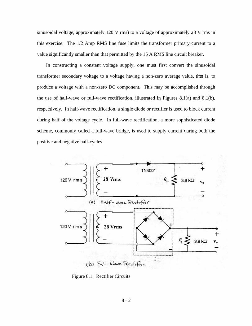
Figure 8.3: Output waveform of half-wave rectifier.
The output voltage across the load resistor is periodic; therefore it can be represented by a
Fourier Series. If the peak instantaneous value of vo is designated by Vo, then
. (8.3)
Inspection of Eq. (8.3) shows that vo consists of a DC component equal to Vo/π. Thus,
the circuit has produced an output voltage that has a non-zero DC component from the
sinusoidal transformer secondary voltage that has a zero DC component. This action of
generating a direct voltage from an alternating supply voltage by a diode is called
rectification. In addition, vo consists of sinusoidal components at the fundamental radian
frequency ω and at integer multiples of ω, called harmonics. Therefore, as a consequence
of the nonlinearity of the diode, the voltage across the load resistor RL contains
components at frequencies not present in the voltage applied to the circuit. Recall that in
circuits consisting entirely of linear elements (resistors, inductors and capacitors), only
frequencies present in the applied voltages and currents can appear.
The rms value of the periodic output voltage, which can be obtained by directly
integrating the square on the half-wave signal shown in Figure 8.8, is given by
(8.4)
from which it follows that
VEFF = Vo(rms) = Vo/2 . (8.5)
8 - 4
⎟⎠⎞
⎜⎝⎛ +−−+= ....4cos
1522cos
32sin
211 tttVoov ω
πω
πω
π
dttVT
rmsVT
oEFFV 22/
0 0 )sin(1)( ω∫≅=
vo
From Equation (8.1), we see that if Rs << RL, then
(8.6)
from which it follows that:
Vo (rms) ≅ Vm/ 2. (8.7)
In addition, the DC or average component of vo can be estimated as:
Vo(DC) ≅ Vm/ π . (8.8)
In the above analysis, an ideal diode model was used. Using a real diode, one must
consider the specifications or maximum rating of the diode to ensure that these ratings are
not exceeded. First, the forward bias voltage of the diode is VD(ON) = 0.7 V for a silicon
diode rather than a short circuit for the ideal diode model. Assuming Vm >> VD(ON), then
the above estimates remain valid.
In addition, an ideal diode can conduct any value of current in the forward direction,
and it remains an open circuit for all values of inverse voltage. This is not the case,
however, with physical diodes. In general, there is a limit to the peak instantaneous
current, id(max), that can be passed without damage; and there is a limit to the peak
instantaneous inverse voltage, vD(piv), that can be applied. Therefore, one must ensure that
these two quantities do not exceed the maximum permissible values in any design.
In the half-wave rectifier, when an inverse voltage exists across the diode, there is no
voltage drop across the circuit resistances since the diode acts as an open circuit under
this condition. In actuality, there is a small amount of reverse leakage current through the
diode, but it can be ignored in this analysis. It follows that the peak inverse voltage is
simply given by:
VD(piv) = Vm . (8.9)
8 - 5
( ) msL
Lmo V
RRR
VpeakV ≅⎟⎟⎠
⎞⎜⎜⎝
⎛+
=

The instantaneous peak forward current occurs when vs has its maximum positive value
and the magnitude of this current is given by:
, (8.10)
where we have assumed VD(ON) << Vm . Further, if Rs << RL, then :
(8.11)
8.2.2 Full-Wave Rectifier
In order to understand the operation of the full-wave rectifier shown in Figure 8.1
(b), consider the circuit shown in Fig. 8.4. Again, the output of the transformer is
represented by a sinusoidal voltage source vs and source resistance Rs, but, as shown, it is
connected to the load resistor RL through a bridge rectifier consisting of four diodes.
Figure 8.4: Full-wave rectifier circuit.
During the positive half cycle of vs, Dl and D3 turn on and act as a short circuit while D2
and D4 turn off and act as an open circuit. Under this condition:
vo = vs - 2(VD(ON)) ≅ vs, (8.12)
where we have assumed 2(VD(ON)) << Vm and that RS << RL. It follows that the peak
voltage across RL will be:
Vo(max) ≅ Vm - 2(VD(ON)) ≅ Vm . (8.13)
8 - 6
Ls
md RR
Vi
+=(max)
.(max)L
md R
Vi ≅
During the negative half cycle of vs, D2 and D4 turn on and act as a short circuit
while Dl and D3 turn off and act as an open circuit. Under this condition:
vo ≅ - vs + 2(vD(ON)) ≅ - vs, (8.14)
since the current through RL is in the same direction as during the positive half cycle.
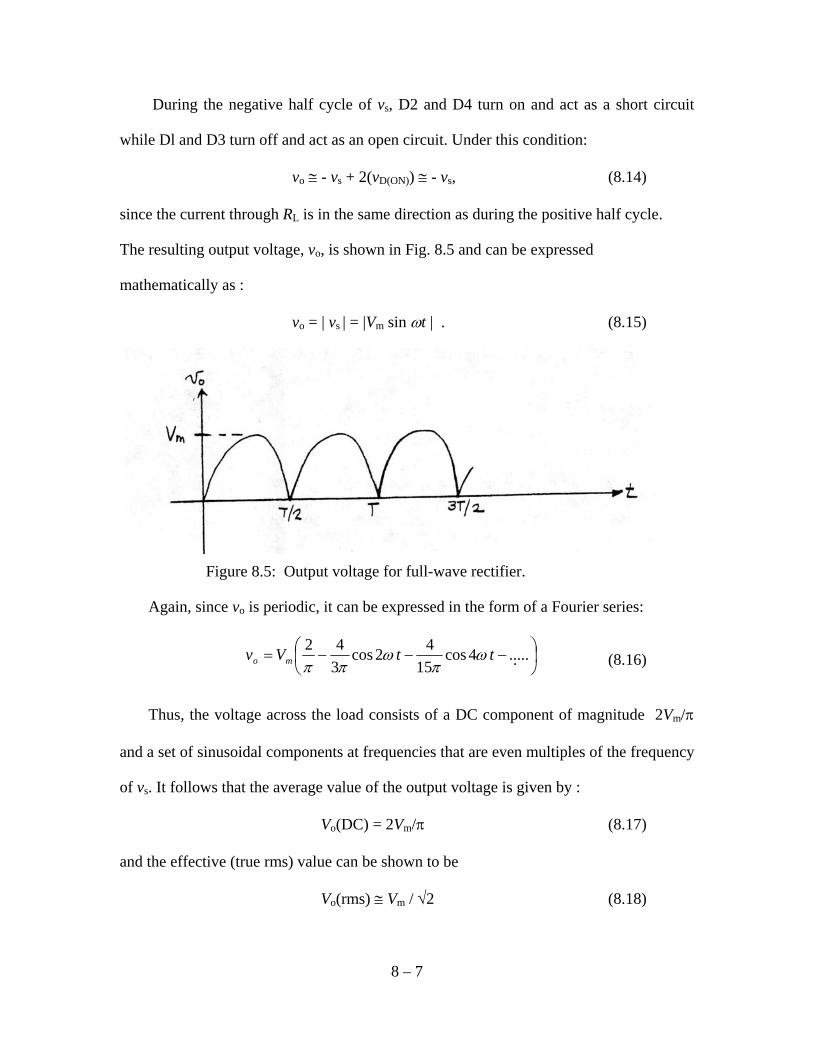
The resulting output voltage, vo, is shown in Fig. 8.5 and can be expressed
mathematically as :
vo = | vs | = |Vm sin ωt | . (8.15)
Figure 8.5: Output voltage for full-wave rectifier.
Again, since vo is periodic, it can be expressed in the form of a Fourier series:
. (8.16)
Thus, the voltage across the load consists of a DC component of magnitude 2Vm/π
and a set of sinusoidal components at frequencies that are even multiples of the frequency
of vs. It follows that the average value of the output voltage is given by :
Vo(DC) = 2Vm/π (8.17)
and the effective (true rms) value can be shown to be
Vo(rms) ≅ Vm / √2 (8.18)
8 – 7
⎟⎠⎞
⎜⎝⎛ −−−= .....4cos
1542cos
342 ttVv mo ω
πω
ππ
Notice that one advantage of full-wave rectification is that the DC value of the output
voltage for the full-wave rectifier is twice the DC value for the half-wave rectifier, i.e.,
2Vm/π compared to Vm/π.
The peak inverse voltage across the diodes can be determined by noting that during
the positive half-cycle of vs, the voltage across D1 is VD(ON) since it is forward biased.
During the negative half-cycle, it is –Vm sin ωt since D1 is reverse biased and operates as
an open circuit. So, it follows that:
VD1(piv) = Vm . (8.19)
A similar analysis shows that the peak inverse voltage for all four diodes is the same,
namely, Vm.
The peak current is given by:
(8.20) where we have assumed that 2 VD(ON) << Vm and Rs << RL . From this, we see that with
the bridge rectifier (4 diodes rather than 1), twice the DC voltage can be delivered to the
load resistor, RL, using diodes with the same instantaneous peak inverse voltage and
maximum current rating.
8.2.3 Half-wave Rectifier with a Capacitor Filter
The half-wave rectifier discussed in Section 2.1 above delivers a pulsating,
unidirectional current to the load and a voltage with a positive DC average but that also
contains a significant AC component. Although this circuit is satisfactory for many
applications (such as a battery charger), it still contains a large AC component which in
our example is equal to a value of 39.6 volts peak-peak. In the design of a DC power
8 - 8
,2 )(
(max)L
m
sL
ONDmD R
VRR
VVI ≅
+
−=
supply, the aim is to produce from the AC power line a constant voltage output with a
minimum of AC content. In order to do this, a means for reducing the AC component of
the output voltage of the half-wave rectifier is necessary.
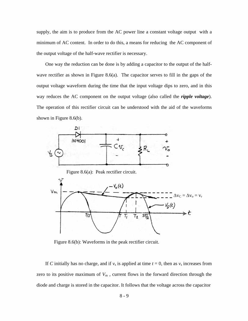
One way the reduction can be done is by adding a capacitor to the output of the half-
wave rectifier as shown in Figure 8.6(a). The capacitor serves to fill in the gaps of the
output voltage waveform during the time that the input voltage dips to zero, and in this
way reduces the AC component on the output voltage (also called the ripple voltage).
The operation of this rectifier circuit can be understood with the aid of the waveforms
shown in Figure 8.6(b).
Figure 8.6(a): Peak rectifier circuit.
Figure 8.6(b): Waveforms in the peak rectifier circuit.
If C initially has no charge, and if vs is applied at time t = 0, then as vs increases from
zero to its positive maximum of Vm , current flows in the forward direction through the
diode and charge is stored in the capacitor. It follows that the voltage across the capacitor
8 - 9
ΔvC = Δvo = vr
vc is essentially equal to vs at every instant of time until vs reaches its maximum value. If
we assume there is no load resistor connected in parallel with the capacitor (i.e., RL = ∞),
then there is no way for C to discharge since the diode doesn't conduct appreciable
current in the reverse direction. In this case, the charge accumulated by C during the first
positive quarter cycle is trapped and cannot escape. This trapped charge maintains the
voltage across the capacitor at the value of Vm, which is the maximum value of the input
voltage as shown by the dotted line in Figure 8.6(b). It follows that this circuit is called a
peak rectifier because its output voltage is equal to the positive peak value of the input
voltage. If we assume RL has a finite but large value, then the capacitor can discharge
slowly through RL while the diode is not conducting. Under these conditions, the output
voltage across the load resistor RL will consist of a small ripple component superimposed
upon a large DC component. This is shown by the solid line labeled vo(t) in Figure 8.6(b).
As RL is made smaller, the capacitor discharges by a greater amount each cycle, and the
ripple component becomes larger in magnitude. Notice that during a brief interval near
the positive peak of vs in each cycle, labeled T1 to T2 between T and 3T/2 in Figure
8.6(b), a pulse of charging current flows through the diode and this pulse restores to the
capacitor the charge lost through RL during the interval when the diode is not conducting.
When the diode is not conducting, the voltage across C will discharge and is given
by: (8.21)
The voltage will continue to discharge until the diode turns back on. The diode will be off
during the remainder of the positive half cycle, and all of the negative half-cycle of vs. It
will turn back on at time T1 when
(8.22)
8 - 10
CRt
mocLeVvv
−==
.sin1
1CR
mmL
TeVV T−
=ω
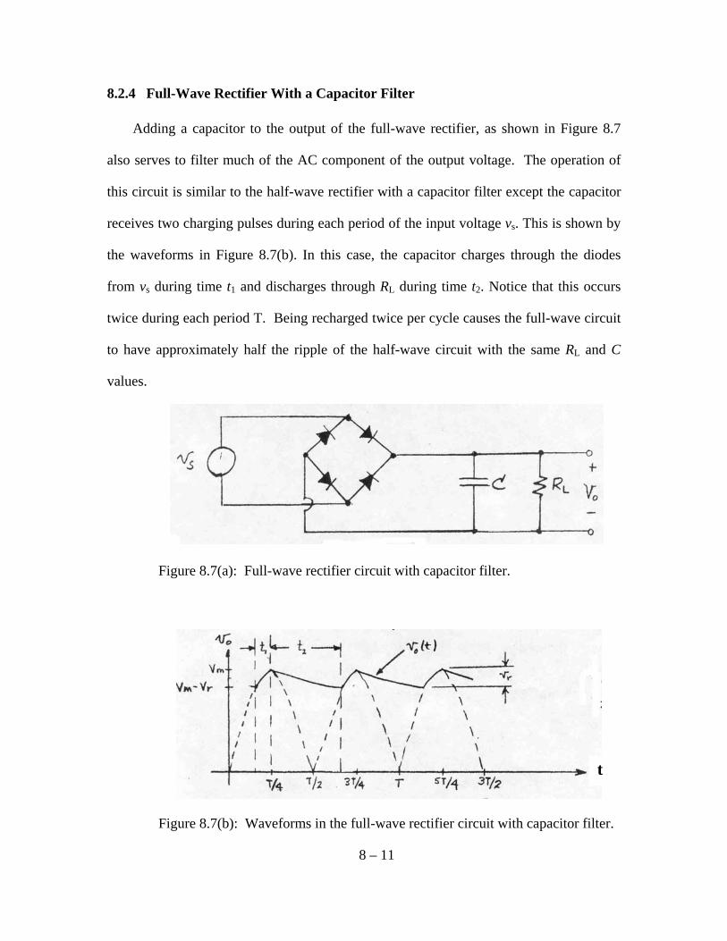
8.2.4 Full-Wave Rectifier With a Capacitor Filter
Adding a capacitor to the output of the full-wave rectifier, as shown in Figure 8.7
also serves to filter much of the AC component of the output voltage. The operation of
this circuit is similar to the half-wave rectifier with a capacitor filter except the capacitor
receives two charging pulses during each period of the input voltage vs. This is shown by
the waveforms in Figure 8.7(b). In this case, the capacitor charges through the diodes
from vs during time t1 and discharges through RL during time t2. Notice that this occurs
twice during each period T. Being recharged twice per cycle causes the full-wave circuit
to have approximately half the ripple of the half-wave circuit with the same RL and C
values.
Figure 8.7(a): Full-wave rectifier circuit with capacitor filter.
Figure 8.7(b): Waveforms in the full-wave rectifier circuit with capacitor filter.
8 – 11
t
When the ripple component of voltage is small compared to the DC component, the
peak-to-peak magnitude of the ripple can be easily estimated. The peak value of vo is Vm
hence, the average value of vo can be written as :
< vo > = Vm – vr / 2, (8.23)
where vr is the peak-to-peak magnitude of the ripple component as shown in Figure
8.7(b). The ripple voltage results from the capacitor discharging through the load
resistor, RL, during the time between charging pulses (as shown by t2 in Figure 8.7(b)).
During this interval, which can be approximated as T/2, i.e., half the period of vs,
since the ripple component is assumed to be small, the output voltage, vo, is nearly
constant at the value Vm. Hence the current discharging C is approximately constant and
can be estimated as:
(8.24)
The charge lost by C while the diodes are not conducting is :
(8.25)
and the corresponding change in the capacitor voltage is :
(8.26)
where vr represents the peak-peak value of the ripple component of vo .
The ratio of peak-peak ripple voltage to the DC output voltage is called the Ripple
Factor (RF) If vr << Vm, then RF is given by
RF ≅ vr / Vm ≅ T/(2RLC) . (8.27)
Since the frequency, f, is f = 1/T = ω / 2π, then it follows that:
RF ≅ π / (ωRLC). (8.28)
The % Ripple is obtained from the Ripple Factor and is given by
% Ripple = RF x 100% = (vr / Vm ) x 100% . (8.29)
8 - 12
.L
mR R
ViL≅
LRiTq2
≅Δ
,22 CR
VTCiTvvv
L
mRrRC
L
L≅≅== ΔΔ

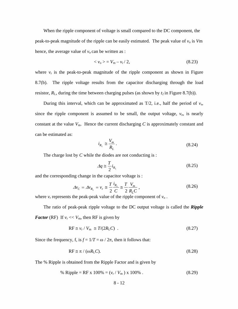
The resultant output voltage waveform for a full-wave rectifier circuit with a 1000μF
capacitor and a 100Ω load resistor is illustrated in Figure 8.8. First note that the scales
are both normalized. So, when the output load voltage is 1, it is equal to the maximum
value of vo, which is Vm, and when the time scale is 1, this is equivalent to one period, T,
of the input voltage.
One of the waveforms provides an illustration of the load voltage without any
capacitor and is indicated by using the " " symbol. The other waveform provides an
illustration of the load voltage with a 1000μF capacitor and is indicated by using the "+"
symbol. Notice that without the capacitor, the normalized peak-peak ripple voltage
component is 1.0 whereas with the capacitor it is reduced to less than 0.1.
As another example, assume the capacitor in Figure 8.7(a) is 1000μF and RL is
3.9kΩ. If we also assume that the transformer secondary output is a 28V rms sinusoidal
signal, then vs = 28√2 sin ωt and the peak or maximum value of the input voltage is 28√2
≅ 39.6 V. It follows that the voltage across the 3.9kΩ load resistor will have a maximum
value of 39.6 V and the resultant average load current, IL, through RL can be estimated as:
IL ≅ (39.6V.)/(3.9kΩ) = 10 mA . (8.30)
It also follows that for the 1000μF capacitor supplying a load current of
approximately 10 mA to the external circuit with a full-wave rectified source at 60 Hz
(Δt = 1/120 second), the ripple will be reduced to 83.3 mV as indicated by using Eq.
(8.26). This is significantly less than the 39.6 V ripple obtained without the 1000μF
capacitor. In this case the Ripple Factor is:
RF = vr / VDC ≅ (83.3mV.)/(39.6V.) = 0.00208 ≈ 0.21% (8.31)
8 - 13
Figure 8.8: Waveforms for the full-wave rectifier circuit.
8 - 14

Another important measure of the performance of a DC power supply is the Voltage
Regulation. This is given by:
Voltage Regulation (VR) = 100% (8.32)
where VNL is the output voltage at no load (i.e., RL = ∞ and IL = 0 ) and VFL is the output
voltage at full load (i.e., IL = IL(max)) . This is an important specification because it
defines the output voltage over the operating range of the power supply. Thus, given a 50
volt DC power supply capable of providing a current of 500 mA with a Load Regulation
of 0.025, it follows that when the supply is providing the maximum current of 500 mA,
its output voltage from Equation (8.30) above is given by
VFL = VNL - VNL* (VR) = 50 - 50 (0.025) = 48.75 V. (8.33)
Exercise 1. Half-Wave Rectifier and Filter Capacitor
(a) Construct the circuit shown in Figure 8.9 below
(b) Use both channels of the oscilloscope to observe the output voltage of the
transformer secondary voltage and the voltage across the 3.9 kΩ resistor. Make a copy of
each waveform noting its shape, periodicity and peak voltage. Take appropriate
measurements with the DMM's and the oscilloscope to determine the average or DC
component, the AC component, and the RMS values of each waveform. Compare your
measurements to the calculated values based upon their peak values.
(c) Using the oscilloscope, make a hardcopy of the waveform across the diode and
measure the diode's forward bias voltage, VD(ON), and the peak inverse voltage, VD(piv).
This can best be done by measuring the voltage across the diode directly using the scope.
(d) Now add a 1 to 10 μF capacitor decade box across RL as shown in dashed lines
in Figure 8.9. Initially set the value of the capacitor to 1μF and copy the output voltage
8 - 15
NL
FLNL
VVV −

across RL compared to the output voltage of the secondary - again noting the waveform
shape, period and peak-to-peak voltage for each signal. Use the DMM and oscilloscope
and measure the DC component and the RMS value of the AC component of the output
voltage across the 3.9kΩ resistor. Increase the value of the capacitor from 1μF up to 10
μF and observe the change in the output voltage. Make a hardcopy and take
measurements at values of 5μF and 10μF, respectively. What happens to the DC and AC
components as the capacitor value is increased?
Exercise 2. Full-Wave Rectifier
Construct the circuit shown in Fig. 8.10 below using the four diode DB102 bridge as
shown. Repeat steps l(b) and 1(c) above. In this case, notice that you can only use the
Figure 8.10: Circuit for Exercise 2
scope to make one measurement at a time because the secondary output of the trans-
8 - 16
28 Vrms
Figure 8.9: Circuit for Exercise 1.
+28 Vrms
-
+
∼
-∼ ∼
∼
+-∼

former is isolated and the ground connection of the scope is not isolated from chassis
ground. First, measure the output voltage of the transformer secondary and then measure
the voltage across the 3.9 kΩ resistor. Also, you can measure the voltage across one of
the diodes within the DB102 bridge by placing the scope probe on the plus (+) side of the
3.9 kΩ resistor and the scope ground on either output of the transformer secondary.
Exercise 3. Full-Wave Rectifier With a Filter Capacitor.
Construct the circuit illustrated in Figure 8.11 with the inductor replaced by a short
circuit. Measure the DC voltage and the peak-to-peak ripple component of the voltage
across RL for DC load currents between 0 and 100 mA using 10 mA increments. Notice
that the load current can be varied by changing the resistance value of the decade resistor
box until the DMM used as a DC ammeter reads the appropriate value. Also, the DC
voltage can be measured with the second DMM and the peak-to-peak ripple voltage can
be measured with the scope AC coupled.
WARNING - (1) This circuit provides NO SHORT CIRCUIT PROTECTION, SO DO
NOT adjust the decade box to all 0's (start off with it set to all 9's) and (2) Note that the
capacitor used in this circuit is electrolytic and; as a result, is polarized and thus must
be connected accordingly.
Figure 8.11: Circuit for Exercise 3.
8 - 17
∼
-
∼ ∼
∼
L
RL
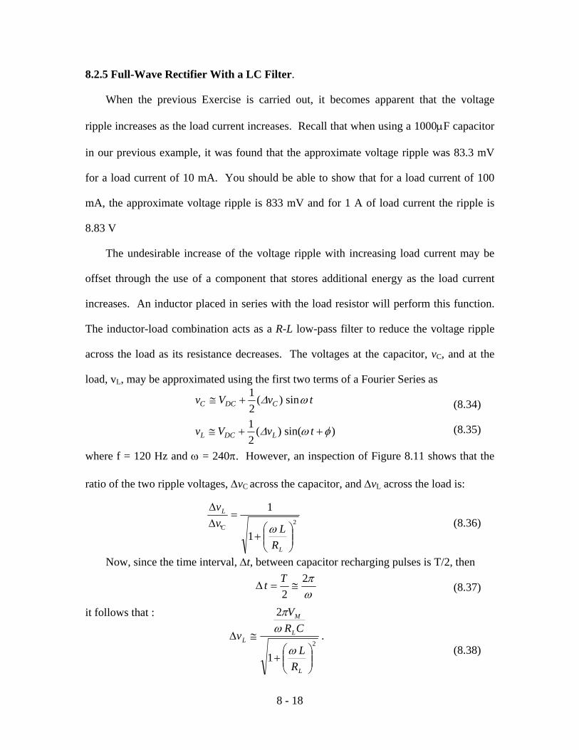
8.2.5 Full-Wave Rectifier With a LC Filter.
When the previous Exercise is carried out, it becomes apparent that the voltage
ripple increases as the load current increases. Recall that when using a 1000μF capacitor
in our previous example, it was found that the approximate voltage ripple was 83.3 mV
for a load current of 10 mA. You should be able to show that for a load current of 100
mA, the approximate voltage ripple is 833 mV and for 1 A of load current the ripple is
8.83 V
The undesirable increase of the voltage ripple with increasing load current may be
offset through the use of a component that stores additional energy as the load current
increases. An inductor placed in series with the load resistor will perform this function.
The inductor-load combination acts as a R-L low-pass filter to reduce the voltage ripple
across the load as its resistance decreases. The voltages at the capacitor, vC, and at the
load, vL, may be approximated using the first two terms of a Fourier Series as
(8.34)
(8.35)
where f = 120 Hz and ω = 240π. However, an inspection of Figure 8.11 shows that the
ratio of the two ripple voltages, ΔvC across the capacitor, and ΔvL across the load is:
. (8.36) Now, since the time interval, Δt, between capacitor recharging pulses is T/2, then (8.37) it follows that :
(8.38)
8 - 18
tvVv CDCC ωΔ sin)(21
+≅
)sin()(21 φωΔ ++≅ tvVv LDCL
2
1
1
⎟⎟⎠
⎞⎜⎜⎝
⎛+
=ΔΔ
L
C
L
RLv
v
ω
ωπ2
2≅=Δ
Tt
.
1
2
2
⎟⎟⎠
⎞⎜⎜⎝
⎛+
≅Δ
L
L
M
L
RL
CRV
vω
ωπ
In the limit of small load resistance, i.e., ωL/RL >> 1, the ripple saturates to a value: vr = (8.39) With ω = 2π (120 Hz) (equivalent to full-wave rectification at 60 Hz) and a 400Ω
load resistor, an inductor L >0.5H is required to reach this limit. As with the approximate
calculations for capacitive filtering this calculation gives an upper limit on the voltage
ripple. The results of a somewhat more exacting, albeit tedious, calculations are shown
in Figure 8.12
Exercise 4. Full-Wave Rectifier with a L-C Filter.
With the 6 Henry inductor installed in the circuit of Figure 8.11, repeat the
measurements of Exercise 3 above.
8.3 Transistor Regulation
The circuit of Figure 8.11 is a substantial improvement over the previous circuits, but
still leaves much to be desired. The voltage ripple is still excessive for many
applications, the output regulation is poor, power is lost in the inductor winding
resistance, and there is no short circuit protection. Additionally, the output voltage is
primarily set by the transformer and is not easily varied. These disadvantages are largely
overcome in the transistor regulator circuit of Figure 8.13.
In this circuit, the output voltage is set by the Zener diode and the transistor base-
emitter forward-bias voltage. With the components shown, the source voltage is 6.2V
(the Zener diode voltage) and the transistor base-emitter junction voltage is ≅ 0.7V. This
gives a load voltage of approximately 5.5V. The 2.7kΩ resistor in series with the Zener
diode maintains a minimum current of 10mA through the diode for all load currents of
8 - 19
LCVv M
L 2
2ωπ
≅Δ
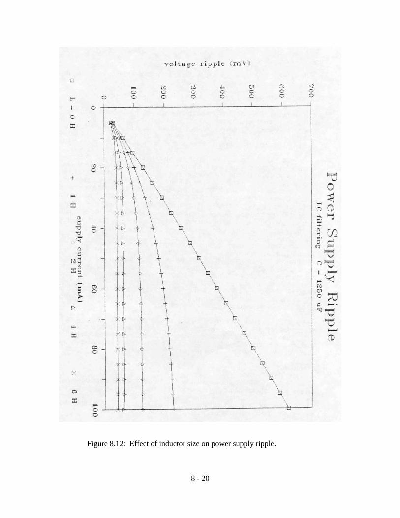
Figure 8.12: Effect of inductor size on power supply ripple.
8 - 20
interest (note the location of the current-limiting resistor), keeping the Zener diode
operating in a region where it has a small differential resistance, defined as Rdif = Δvz/Δiz .
Thus, moderate changes in the resistor-diode series voltage will result in proportional
changes in the current through these components, but will produce only minute changes
in the Zener diode voltage.
The transistor serves to deliver relatively large currents to the load with a relatively
small current in the resistor-Zener diode circuit. The 2N3055 transistor used here has a
DC current gain of approximately 40 so that a load current of 100mA draws a mere
2.5mA from the base-biasing circuit. The reverse-biased collector-base junction is
capable of withstanding any voltage less than the reverse-voltage breakdown value for
this transistor, which is 60V. Consequently, this circuit will regulate the output voltage at
approximately 5.5V as long as the collector-base voltage isn’t less than 0.5V (the onset
of saturation) or greater than 60V (the onset of voltage breakdown in the transistor).
Note that one of performance criteria for transistor regulators is the Ripple Rejection
(RR). RR is the ripple voltage across the load divided by the ripple voltage across the
capacitor in decibels., i.e.,
RR = 20 log10 (vRL/vC) (8.40)
Exercise 5. Transistor Regulator.
(a) Construct the circuit of Figure 8.13. Use the DMM's to record VZ(DC) and
VLoad(DC) as the load resistor is varied from 1MegΩ to 50Ω in a 1, 0.5, 0.2 ...sequence.
(b) With a load resistor of 50Ω, record the DC and AC voltages across the 500μF
capacitor and the DC and AC voltages across the 50Ω load resistor using the DMMs.
8 - 21

Figure 8.13: Transistor regulator circuit.
8.4 Active Regulation
The circuit of Figure 8.13 performs quite well for all but the most demanding
applications, and yet has a few drawbacks. The output is not continuously variable, being
set by the choice of Zener diode, and there is no compensation for drift in the output
voltage. This latter is particularly important due to the lack of temperature compensation
for changes in the base-emitter forward bias voltage and variation in DC current gain as
the transistor dissipates power and gets warmer. While there are many simple schemes
for incorporating temperature compensation and adjustments for deviations in the output
voltage, we will not pursue these, but instead we will turn our attention to commercial
integrated circuit regulators such as the LM317, which is used in the circuit of Figure
8.14. Conceptually, the LM317 is quite similar to the regulator circuit employed
previously but with numerous refinements. Under proper operating conditions it
exhibits good regulation as the load or input voltage is varied, with a small current
through the adjust terminal so that the input current is nearly identical to the load current.
The LM317 also employs a significant amount of compensation circuitry to insure a
8 - 22
500 μF
500μ
CB
120V 60Hz
120/28
10 W
Regulator Circuit
F

Figure 8.14: Active regulator circuit
stable output voltage (i.e., non-oscillatory) over a wide range of operating conditions. An
idealized equivalent circuit for this device is shown in Figure 8.15. The similarities
Figure 8.15: Simplified circuit model for the LM317 regulator.
between this model and that for an ideal active transistor should be apparent. Vref is the
output voltage, which is set internally to 1.2V for the LM317. Other commercial
regulators have output voltages that are more commonly required. An example is the
LM7805, which has an output voltage, non-variable, of 5V. For the LM317, proper
operation requires that the input to output voltage difference remain between 3V and 40V
and that the output terminal current be at least 10mA. Under these conditions the
8 - 23
500μF
manufacturer specifies a maximum output load voltage regulation of 0.5% (or
25mV if Vin – Vout < 5V), a maximum regulation due to change in input voltage of
0.07% per Volt of change in the input, and a typical ripple rejection of 65dB with full
wave rectification at 60 Hz.
An output voltage of 1.2V from the LM317 may, at first glance, seem to have limited
utility, but with the proper circuit connections it may be used to produce a regulated
output voltage of almost any value. Consider the circuit of Figure 8.14. A current of
5mA (1.2V/ 240Ω) passes through the 240Ω resistor. Since the current in the adjust
terminal is quite small, (typically 50μA.) and stays substantially constant as the load
current varies, any reasonable resistor value connected between the adjust terminal and
the power supply common will also conduct 5mA. In this way the LM317 may be used
as a constant current source, where the constant current emanates from the adjust terminal
and the 240Ω resistor. To construct an approximate 5V source we need merely to
connect a 750Ω resistor in this location. The voltage across this resistor is then 3.75V,
which causes the net output voltage to common to be 4.95V. Any additional current
required by a load resistor is supplied by the regulator output without affecting the output
voltage that remains at 4.95V.
Exercise 6. Active Voltage Regulator
Construct the circuit illustrated in Figure 8.14 and measure the output voltage and
ripple for load currents between 0 and 100mA.
8.5 Report
8.5.1 Show a copy of the load resistor voltage observed for the half-wave rectified
8 - 24
unfiltered circuit. What was the DC component and RMS voltage from your
measurements and how does this compare to the calculated values? Now, show a copy of
the voltage waveform observed across the diode and indicate the value of the forward
biased and peak inverse voltages that you observed.
8.5.2 Show the load resistor voltages observed for the half-wave rectified circuit with
the 1μF capacitor compared to the 10μF capacitor. Using your measured values, specify
the DC output voltage and determine the % ripple for values of 1μF, 5μF, and 10μF.
8.5.3 Show the load resistor voltage observed for the full-wave rectified unfiltered
circuit. What were the DC component and RMS values from your measurements and
how do they compare to the calculated values? Next present the copy of the voltage
waveform observed across one of the diodes and indicate the value of the forward bias
and peak inverse voltages that you measured.
8.5.4 Use your data to construct a table and plot the values of the DC and ripple
components of the load voltage as a function of load current for the full-wave rectified
circuit with just the capacitor as filter. How does the ripple component measured in VL
compare to estimates obtained from calculated results assuming only a capacitor is used
as a filter? What is the load voltage regulation for this DC supply? What is the % ripple
at full load?
8.5.5 Repeat the table and plot for the circuit using the LC filter. What is the voltage
regulation and % ripple at full load for this supply? Why is the average DC output of this
supply less than the one when only the capacitor was used? How does the load regulation
and % ripple of this supply compare with the one that only used a capacitor? Finally, if
you wanted to use this supply but needed the same DC output as the supply with only a
capacitor as a filter, what change could you make?
8 - 25
8.5.6 For Exercise 5, make plots on the same graph of VZ(DC) and VRL(DC) versus RL
using a log scale from 50 Ω to 1 MΩ. Calculate load Voltage Regulation (VR) in
percent. What causes it to differ from 0%? What was the ripple voltage at RL = 50 Ω?
Compute the Ripple Rejection (RR) in dB for RL = 50 Ω. For a load of 50 Ω, calculate
the power dissipated by the transistor and by the 100 Ω current limiting resistor.
8.5.7 Describe the performance of the LM317 regulator used in this experiment. How
did the output voltage vary as the load current approached zero? What voltage ripple was
observed and what was the voltage regulation of the circuit? Does the LM317 meet the
performance specifications given by the manufacturer that are applicable here?
8.5.8 Design Problem - Design a DC power supply, similar to the one shown in
Figure 8.11, that includes a full wave bridge rectifier (DB 102) and filtering provided by
an inductor and a capacitor. The power supply should satisfy the following
specifications.
Power source: 120 V, 60 Hz, Single Phase AC
Output current: 1000 mA max
Output voltage: 11 VDC at half load (500mA) and 10VDC at full load (1000 mA)
Ripple voltage: Less than 0.3 Vp-p for all currents.
The design documentation should include the following:
1. A schematic diagram of the power supply circuit,
2. The voltage ratio for the transformer,
3. The selected capacitor and inductor values and inductor coil resistance,
4. Verify that ripple voltage specifications are met,
5. Calculate the output voltage at 100 mA.
8 - 26