Embed Size (px)
Citation preview

Abstract—In this work, a characterization of coupled
transmission lines used in integrated circuit packaging on
printed circuit boards is presented. The method proposed is
based on the method of moments and mathematical model based
on analytical equations for fast extraction of parameters per unit
length of coupled transmission lines lossless. The charge
distribution is evaluated only once using the method of moments,
in order to calculate per unit length parameters of capacity
matrix in the presence of substrate. The elements per unit length
of inductance matrix are then calculated by mathematical model
based on analytical and empirical equations.
Index Terms—Method of moments, multiconductor lines
parameters per unit length, packaging, PCB.
I. INTRODUCTION
The industrial constraints evolution causes a break in the
designing of printed circuit boards (PCBs). Today, the PCB
must present a panel of analog and digital functions largest. It
is necessary that all of these functions are integrated on
smaller and smaller supports, and they are increasing speeds. However, this evaluation also leads to a degradation of signal
quality and increase electromagnetic interference in the PCB
cards. For that PCBs and their elements (edge connectors,
microstrip lines), must be modeled using the transmission line
methodology [1]-[4].
In this article, a characterization of coupled transmission
lines used in integrated circuit packaging on printed circuit
boards is presented. We have chosen the method of moments
and mathematical model based on empirical equations for fast
characterization, and in order to simplify the extraction
method for coupled microstrip transmission line. Matrix
capacity C is computed only once in the presence of the
substrate, by evaluating the corresponding charge distribution,
using the method of images, the pulse basic function, and
point matching of the method of MoM [7], [8]. The
parameters per unit length of inductance matrix are then
calculated analytically from a mathematical model in
MATLAB routines based on analytical and empirical
equations. For a coupled transmission lines characterization,
Manuscript received February
6, 2013; revised April 10, 2013. This work
was supported in part by Campus France and GREMAN laboratory.
Nassima
Tidjani, Ali
Ouchar
are with
University
of Laghouat,
Algeria
Jean-Charles Le
Bunetel,
Yves
Raingeaud
are with
University of
François-
Rabelais, Tours, France
we have realized two PCBs, PCB I, and PCB II for one and
two coupled transmission lines. Also PCB III is used with
three coupled transmission lines. The measurements are
performed by precision impedance analyzer 4294A, the
calculations and simulations are done by Matlab routines and
electromagnetic simulator Microwave office [9], [10].
II. INTEGRAL EQUATIONS THEORY
2 2
0
1( ) ( ).ln ( ) .
2. .
W
lV r r x x y dx
(1)
r',
r
positions
of source point,
and
of
N
sections
of
uniform
width
Δ
“Fig.1”, and we
used the
pulse basic function
Pn(x).
The pulse basic function
is defined
0
Δ
2Δ
3Δ
N
Δ
Fig. 1. Discretization of the strip into N segments.
The sum of the charges
on
the N
segments
is equal
to the
total charge. αn
is the unknown charge
density
on a
segment
n
1
( ) ( )
N
l n n
n
r P r (2)
When we replace “(2)” in “(1)”, it
will generate
N
equations
by evaluating
“(3)”
at N-point
along the strip. It
is
segmented into
N
computing the
potential
at the center
of each
segment.
We
assumed
constant
potential
on each segment.
xm
is the
position
in the middle of
segment
m.
For m
from 1 to N,
we can write:
1
2 2
1
1( ) ( ) ln ( )
2
n
n
xN
m n n m
n x
V x P x x x y dx
(3)
We introduce the
boundary conditions
V(r)=V=1. The final
system
of equations
in matrix form is given by “(4)”.
.V Z (4)
With:
Coupled Transmission Lines Used in Coupled Transmission Lines Used in
Integrated Circuit Packaging on Printed Circuit Boards
N. Tidjani, J. C. Le Bunetel, A. Ouchar, and Y. Raingeaud
corresponds to the
72
International Journal of Computer and Electrical Engineering, Vol. 6, No. 2, April 2014
DOI: 10.7763/IJCEE.2014.V6.797
Characterization of
Several methods treated the transmission lines modeling by
the parameters per unit length evaluation. Among these
methods, the finite element method, invariance method, and
method of moments (MoM) [5], [6].
We consider a microstrip line of width W, which carrier a
per unit length charge density ρl, assuming a zero- thickness
strip, the potential can be written as follows [11], [12]:
observation point respectively. We divide the strip width W of
unitary on the segment Δ and zero otherwise [4].
[13].

1
2 21ln ( )
2
n
n
x
mn m
x
Z x x y dx
(5)
We have for m=n:
2 2
1
11 ln 2 ln 2 4
2. . 4. .
2 8 tan 4
mnZ d
dd
(6)
And for m≠n:
2
2 2
21 1
2 2
22 ln 2
2. . 2 4
2 2 2 ln 4 tan tan
2 22 4
mnlmn mn mn
mn
mn mn mn
mn
Z
d
dd dd
(7)
We set B=Z-1
, we can find the total charge distribution Q
.
ij
row n
Q B (8)
At first we calculate the total charge distribution Q
with
substrate by the method of moment. The method of moment
divides each
strip of width
W
into N
uniform
sections
and uses
the pulse basic function. Then the parameters per unit length
of capacitance matrix C are given for unitary voltage V
from
“(1)”.
Q CV (9)
We use the telegraph equation “(10)” for coupled
transmission lines.
11 12
21 22
( , ) ( , )
L LV z t I z t
L Lz t (10)
where L11, L22
are the inductance
of line 1, line 2 respectively.
L12, L21
are the mutual
inductance between line 1 and line 2.
For two symmetrical microstrips we put:
L12=L21=Lm, and L11=L22=L.
The inductance matrix in
equation “(10)” can be extended up to N transmission lines
as
follow [14]:
11 12 1
21 22
1
. .
. . .
. . . . .
. . . . .
. . .
N
N NN
L L L
L L
L
L L
(11)
The parameters Lii of the matrix inductance depend only on
the geometry of the lines, these elements can calculate from
“(12)”. The mutual parameters Lij are calculated from the
empirical equation in “(13)”. The valid ranges of the
geometry parameters for the derived equation are summarized
in Table I. With H is the substrate height, W
the strip width, T
the strip height, S the strips separation,
v0
the light speed, µ0
the vacuum permeability.
TABLE I:
VALID RANGES OF THE GEOMETRY PARAMTERS
0
1
0
60 8ln 1
4
120ln 1.393 0.667 ln 1.444 1
ii
H W W
v W H HL
W W W
v H H H
(12)
0.16 1.18 2.6
0
2.03 0.13 1.09
0.415 2.38 1.07
+ 0.89 0.418 1.37
m
H T SL
W W H
S H T
H W W
(13)
IV.
VALIDATION AND MEASUREMENT
We
have
realized a PCB I
with one
microstrip line
deposited on the
dielectric FR4, and PCB II
contains
coupled
microstrip
line. Also we have simulated
PCB III with tree
coupled microstrip.
The characteristics of PCB I, PCB II, and PCB III
are
summarised
in Table II.
The different
measurement
steps of
parameters per unit length are
summarized in figures (1-5).
Fig.
2.
and
Fig. 3.
illustrate
the
capacitance C0,
and
inductance
L0
measurement, on
PCB
I
In Fig.
2.
we put the impedance analyzer probe
in the first
connector
with adapter, and we allow
the second connector
open.
We find the capacitance expression C0
by “(14)”
in
0 2 meas con adaC C C C l (14)
Also in Fig.
3,
we
put the probe in the first connector,
and
we allow the second connector in short circuit.
The
inductance expression L0
is
given
by “(15)”
in function of
0 meas GNDL L L l (15)
H
0.1 mm H 1.52 mm
T
17.2 mm T 69.5 µm
S/H
0.25 S/H
3.75
W/H
0.1 W/H
5
S/W
0.14 S/W
4
73
International Journal of Computer and Electrical Engineering, Vol. 6, No. 2, April 2014
III. PARAMETERS PER UNIT LENGTH
function of measure Cmeas, connector capacitance Ccon, and
adapter capacitance Cada.
measure Lmeas, and ground plane inductance LGND.

TABLE II:
DIMENSIONAL PARAMETERS OF TEST STRUCTURES
Different PCBs
Schematics Dimensions
PCB I
One microstrip
W=2.94mm
H=1.5mm
εr=4.7
Length=10 cm
PCB II
Two microstrips
W=2.94mm
H=1.5mm
εr=4.7
S=3mm
Length=10cm
PCB III
Three microstrips
W=2.6mm
H=1.5mm
εr=4.3
S=1.5mm
Length=20.1cm
Probe
Short
circuit
Fig. 3. Inductance
L0
measurement.
Fig. 4. Mutual capacitance
Cm
measurement.
PPoorrtt 11
PPoorrtt 22
PPoorrtt 33
PPoorrtt 44
Probe
Fig. 5. Mutual
inductance
measurement
L meas1
Fig. 6. Mutual
inductance
measurement
L meas2
For the mutual inductance
measurement
Lm
we have done
two measures that are illustrated
in Fig.
5.
and
Fig. 6.
In
Fig.
5.
we put the probe in port 1, connect port 2 and port 3
with a
cable, and put port 4 in short circuit. The expression of
measure is given by “(17)”.
1 2 2meas m GND cableL L L L L (17)
Also in Fig.
6.
we put the probe in port 1, connect port 2
and port 4 with the same cable as the first measurement, and
put port 3 in short circuit. The expression of measure is
given
by “(18)”.
2 2 2meas m GND cableL L L L L (18)
From these two measures we can find the expression of the
mutual inductance Lm
by “(19)” in function of Lmeas1, and
Lmeas2. The advantage of this method that the effects of the
cable, ground plane, and strip are subtracted.
1 2 m meas measL L L l (19)
Finally, we can write all parameters per unit length of
inductance and capacitance matrices in function of the done
measurement, for symmetrical two coupled transmission lines
by “(20)-(23)”.
11 0L L (20)
12 mL L (21)
12 mC C (22)
11 0 mC C C (23)
V. RESULTS AND INTERPRETATION
The Fig. 7. and Fig. 8. summarize the charge distribution,
on the transmission line in PCB I depending by the position.
We observe that the charge distribution has a low variation in
Air
Dielectric
W
H
S
74
International Journal of Computer and Electrical Engineering, Vol. 6, No. 2, April 2014
l
ProbeOpen
circuit
Fig. 2. Capacitance C0 measurement.
the center, and augment at the edge of the strip, which is due
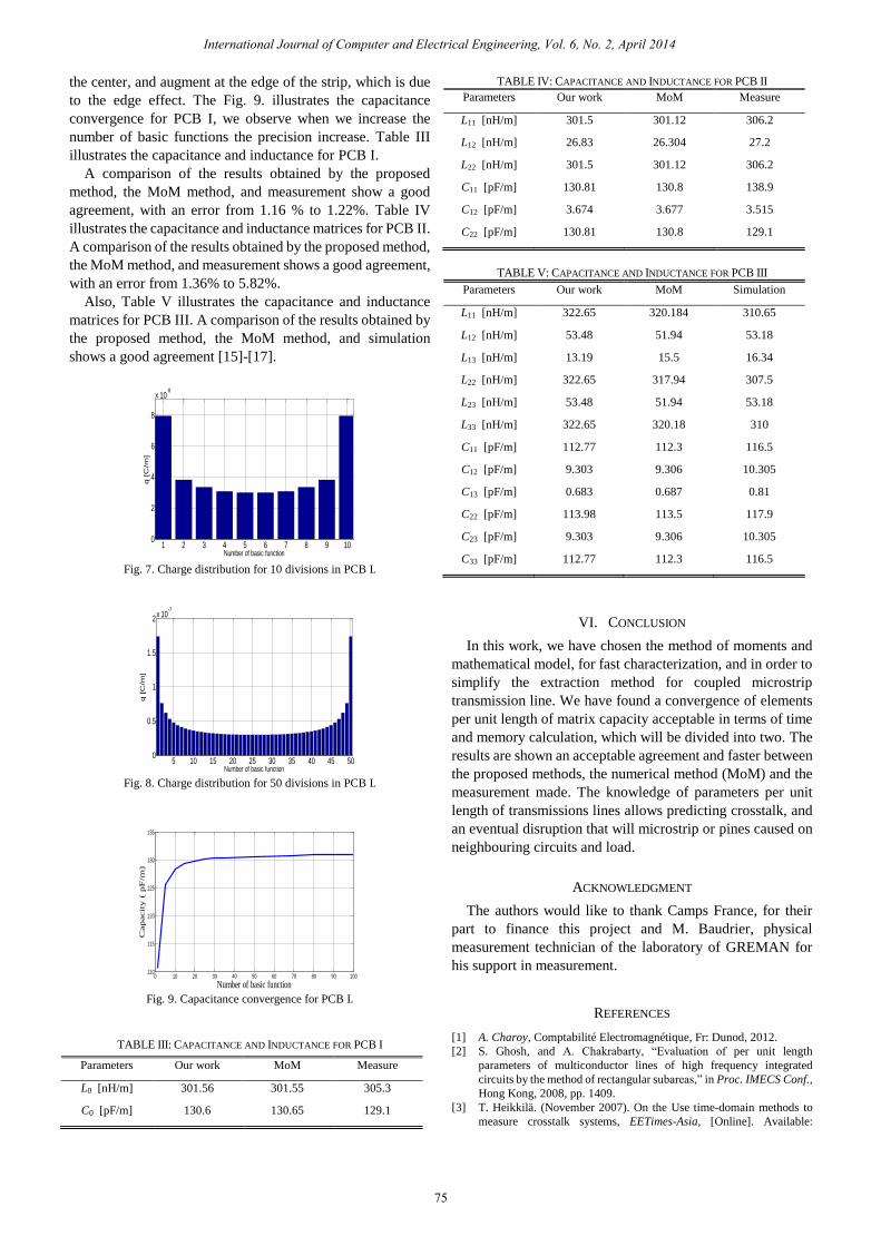
to the edge effect. The Fig. 9. illustrates the capacitance
convergence for PCB I, we observe when we increase the
number of basic functions the precision increase. Table III
illustrates the capacitance and inductance for PCB I.
A comparison of the results obtained by the proposed
method, the MoM method, and measurement show a good
agreement, with an error from 1.16 % to 1.22%. Table IV
illustrates the capacitance and inductance matrices for PCB II.
A comparison of the results obtained by the proposed method,
the MoM method, and measurement shows a good agreement,
with an error from 1.36% to 5.82%.
1 2 3 4 5 6 7 8 9 100
2
4
6
8
x 10-8
Number of basic function
q [C
/m]
Fig. 7. Charge distribution for 10 divisions
in PCB
I.
5 10 15 20 25 30 35 40 45 500
0.5
1
1.5
2x 10
-7
Number of basic function
q [C
/m]
Fig. 8. Charge distribution for 50 divisions in PCB I.
0 10 20 30 40 50 60 70 80 90 100110
115
120
125
130
135
Number of basic function
Capacit
y (
pF
/m)
Fig. 9. Capacitance convergence for PCB I.
TABLE
III:
CAPACITANCE AND INDUCTANCE FOR PCB
I
Parameters
Our work
MoM
Measure
L0
[nH/m]
301.56
301.55
305.3
C0
[pF/m]
130.6
130.65
129.1
TABLE
IV:
CAPACITANCE AND INDUCTANCE FOR PCB
II
Parameters
Our work
MoM
Measure
L11 [nH/m]
301.5
301.12
306.2
L12 [nH/m]
26.83
26.304
27.2
L22 [nH/m]
301.5
301.12
306.2
C11
[pF/m]
130.81
130.8
138.9
C12 [pF/m]
3.674
3.677
3.515
C22
[pF/m]
130.81
130.8
129.1
TABLE
V:
CAPACITANCE AND INDUCTANCE FOR PCB
III
Parameters
Our work
MoM
Simulation
L11 [nH/m]
322.65
320.184
310.65
L12 [nH/m]
53.48
51.94
53.18
L13 [nH/m]
13.19
15.5
16.34
L22 [nH/m]
322.65
317.94
307.5
L23 [nH/m]
53.48
51.94
53.18
L33 [nH/m]
322.65
320.18
310
C11
[pF/m]
112.77
112.3
116.5
C12 [pF/m]
9.303
9.306
10.305
C13
[pF/m]
0.683
0.687
0.81
C22
[pF/m]
113.98
113.5
117.9
C23
[pF/m]
9.303
9.306
10.305
C33
[pF/m]
112.77
112.3
116.5
VI.
CONCLUSION
In this work,
we have chosen
the method of moments and
mathematical model, for fast characterization, and in order to
simplify the extraction method for coupled microstrip
transmission line.
We have found a convergence of elements
per unit length of
matrix capacity acceptable in terms of time
and memory
calculation, which will be divided into two.
The
results are shown an acceptable agreement and faster
between
the proposed methods, the numerical method
(MoM) and the
measurement made.
The knowledge of parameters per unit
length of
transmissions lines allows
predicting crosstalk, and
an eventual disruption that will microstrip or pines caused on
neighbouring
circuits and load.
ACKNOWLEDGMENT
The authors would like to thank Camps France, for their
part to finance this project and M. Baudrier, physical
measurement technician of the laboratory of GREMAN for
his support in measurement.
REFERENCES
75
International Journal of Computer and Electrical Engineering, Vol. 6, No. 2, April 2014
Also, Table V illustrates the capacitance and inductance
matrices for PCB III. A comparison of the results obtained by
the proposed method, the MoM method, and simulation
shows a good agreement [15]-[17].
[1] A. Charoy, Comptabilité Electromagnétique, Fr: Dunod, 2012.
[2] S. Ghosh, and A. Chakrabarty, “Evaluation of per unit length
parameters of multiconductor lines of high frequency integrated
circuits by the method of rectangular subareas,” in Proc. IMECS Conf.,
Hong Kong, 2008, pp. 1409.
[3] T. Heikkilä. (November 2007). On the Use time-domain methods to
measure crosstalk systems, EETimes-Asia, [Online]. Available:

Nassima Tidjani
received her Magisterium
degree in electromagnetic compatibility in the
electrical system from the university of Laghouat
in Algeria in 2007, currently she is a PhD student
in laboratory of GREMANat in university of
Tours in France, her research interests are system
modeling in EMC and Microwave, transmission
lines , crosstalk , reduction method, at the
GREMAN Laboratory, Tours, France.
Jean-Charles Le Bunetel received the Ph.D.
degree in electrical engineering from the
University of Havre, LEPII laboratory, Le Havre,
France, in 1997. He is currently Assistant
Professor at the François Rabelais University,
GREMAN, Tours, France. His research interests
include power electronics, converter structures,
EMI modeling, and associated EMC problems at
the GREMAN Laboratory, Tours, France.
Ali Ouchar
received the Ph.D. degree in
telecommunication engineering from the
Polytechnic
of El Harach,
Algiers, Algeria, in
2002. He is currently Professor at the university of
Laghouat, Algeria. He is Director
of the research
laboratory
LEDMASD
in Laghouat
in 2006.
Member
of the photonic
network, and
of
renewable
energy
network
Algiers. His research
interests EMC problems, microwave
devices,
and
fiber optics.
Yves Raingeaud received the Ph.D. degree in
electrical engineering from the University of
Limoges, IRCOM laboratory, Limoges, France, in
1993. He is currently Assistant Professor at the
François Rabelais University, GREMAN, Tours,
France. His research interests include power
electronics switches, EMI modeling, and
associated EMC problems at the GREMAN
Laboratory, Tours, France.
Author’s formal
photo
formal photo
Author’s formal
photo
76
International Journal of Computer and Electrical Engineering, Vol. 6, No. 2, April 2014
http://www.eetasia.com/ARTICLES/2007NOV/PDF/EEOL_2007NO
V16_TPA_EDA_TA.pdf?SOURCES=DOWNLOAD.
[4] T. Magesacher,“MTL-a multi wire transmission line modeling
toolbox,” International Journal of Computer and Electrical
Engineering, vol. 5, no. 1, pp. 52-55, February 2013.
[5] S. Musa, M. Sadiku, and J. Clark, “Finite element analysis for
electromagnetic parameters of multiconductor interconnects in
multilayered dielectric media,” International Journal of Advances in
Applied Sciences, vol. 1, no. 4, pp. 181-190, December 2012.
[6] E. Metlevskis, “Analysis of rectangular microstrip structures by the
method of moments,” in Proc. of 18th International conference on
microwave radar and wireless communications, Vilnius, 2010, pp.
1-4.
[7] R. Clayton, Introduction to electromagnetic compatibility, 2nd edition,
USA: John wiley & Sons, 2006.
[8] W. Gibson, The Method of Moments in Electromagnetics, USA:
Taylor & Francis Group, 2006.
[9] Y. Sohn, J. Lee, H. Park, and S. Cho, “Empirical equations on
electrical parameters of coupled microstrip lines for crosstalk
estimation in printed circuit board,” IEEE Trans on Advanced
Packaging, vol. 24, no. 4, pp. 521-527, 2001.
[10] K. Soorya Krishna, S. Bhat, “Impedance matching in multi-layer
interconnect structures to minimize signal reflections in high speed
application,” International Journal of Computer and Electrical
Engineering, Vol. 4, No. 3, pp.345-349, June, 2012.
[11] F. Gardiol, Traité d’électricité: Electromagnétisme, Fr: Presses
Polytechniques et Universitaires Romandes, 1996, vol. 3.
[12] Pérez, R. Carles, and R. Fleckinger, Électromagnétisme: Fondements
et Applications, Fr: Dunod, 2001.
[13] N.Tidjani, J. Le Bunetel, and A. Ouchar, “Crosstalk analyses in
coupled transmission lines used in telephony mobile,” 17th IEEE
Signal and Power Integrity, pp.155-158, Paris, 2013.
[14] R. Clayton, Analysis of Multiconductor Transmission Lines, USA:
John Wiley & Sons, IEEE Press, 2008.
[15] Microwave office getting started guide, AWR design environment,
2009.
[16] RF High Power Product Model Design Kits, AWR Corporation
Microwave Office, 2011.
[17] I. Novak and B. Eged, “Measurement by vector network analyzer and
simulation of crosstalk reduction on printed circuit boards with
additional center traces,” IEEE Instrumentation and Measurement
Technology, pp. 269-274, Irvine, 1993.