Embed Size (px)
Citation preview
Chapter 1
Hardware Metering: A Survey
Farinaz Koushanfar
Abstract This chapter provides the first comprehensive overview of hard-ware integrated circuits (IC) protection by metering. Hardware metering, orIC metering refers to mechanisms, methods, and protocols that enable track-ing of the ICs post-fabrication. Metering is particularly needed in the hori-zontal semiconductor business model where the design houses outsource theirfabrication to (mostly offshore) contract foundries to mitigate the manufac-turing and labor costs. The designers and/or the design intellectual property(IP) holders are vulnerable to piracy and overbuilding attacks due to thetransparency of their designed IP to the foundry that requires a complete de-scription of the design components and layout to fabricate the chips. Becauseof the prevalence of counterfeit and overbuilt items, and the widespread usageof ICs in a variety of important applications, the problem has recently gainedan increased attention by the industry, government, and research community.Post-silicon identification and tagging of the individual ICs fabricated by thesame mask is a precursor for metering: In passive metering, each ICs is specifi-cally identified, either in terms of its functionality, or by other forms of uniqueidentification. The identified ICs may be matched against their record in apre-formed database that could reveal unregistered ICs or overbuilt ICs (incase of collisions). In active metering, not only the ICs are uniquely identified,but also parts of the chip’s functionality can be only accessed, locked (dis-abled), or unclocked (enabled) by the designer and/or IP rights owners witha high level knowledge of the design that is not transferred to the foundry.We provide a systematic view of the field, along with the first detailed tax-onomy and descriptions of the various passive and active hardware meteringmethods available.
Electrical and Computer Engineering Department, Rice University
1
2 Farinaz Koushanfar
1.1 Introduction
As the integrated circuits scale in feature sizes and exponentially grow in func-tionality, they also become increasingly complex. The sophisticated chips indesign and fabrication today require costly, intricate, and complex processesthat can only be performed in state-of-art fabrication facilities. Building ormaintaining such facilities for the present CMOS technology is reported tobe more than 3 Billion dollars and growing, described as the most expensivefactories ever built by humankind [30, 40]. Given this increasingly glowingcost and complexity of foundries and their processes, the semiconductor busi-ness model has largely shifted to a contract foundry business model (a.k.a.horizontal business model) over the past two decades. For example, Texas In-struments (TI) and Advanced Micro Devices (AMD), two chip making giantsthat have traditionally used their in-house facilities for fabricating their chips,have both recently announced outsourcing most of their sub-45nm fabricationto major contract foundries worldwide.
In the horizontal business model, the relationship between the designerand the foundry is asymmetric: the designed IP is transparent to the manu-facturers who can reproduce (overbuild) the ICs with a negligible overheadbecause of the ready availability of the masks; but the details of the fabrica-tion process, quantity, and possible modifications to the original designer’schip blueprint (in form of layout files such as OASIS format) are clandestineto the design house. The existing business model and contract agreements areinsufficient for full protection of the designer IP rights [1, 2]. The IP ownersdisclose the details of their IP and also pay for building costly masks basedon their designs; they trust the foundry not to pirate their designs and notto overbuild more ICs. The mask’s ready availability at the foundry, relativelow cost of silicon, and lack of designer’s (IP rights owner’s) control over thefoundry fabrication further ease piracy. The internal of the manufactured ICsare opaque due to the design’s multiple layers and its complexity; interfacecircuitry that only allows limited external access to certain internal chip com-ponents; and the packaging. What exacerbates the problem is that the ICsare exploited for multiple applications with strict anti-cloning and securityrequirements, including but not limited to bank cards, security devices, andweapons. Given the criticality of applications and designer’s huge losses topiracy, preventing IC theft, piracy, and overbuilding by the contract foundrieshave become increasingly crucial from the government, industry, business andconsumer point of views.
IC metering is a set of security protocols that enable the design houseto achieve post-fabrication control over their ICs. The term “hardware me-tering” was first coined in 2001 [26, 25] to refer to the first passive methodfor uniquely tagging each IC’s functionality while maintaining the same in-put/output behavior and synthesis flow. Around the same time and inde-pendently, methods for unclonable identification of ICs including physicalunclonable functions (PUFs) have been in development [28, 14]. Since then,
1 Hardware Metering: A Survey 3
multiple newer methods for giving a design house (IP rights over) controlover their designs have been proposed for metering. Note that the levels ofpost-fabrication protection and control are dependent on the attack model,the desired protection level, and the security assumptions for the IC supplychain.
The focus of this chapter is on hardware metering. It is important toemphasize the difference between hardware watermarking and hardware me-tering. While metering attempts to uniquely tag each chip produced from acertain design by active or passive methods to facilitate tracing the chips,watermarking’s objective is to uniquely tag the design itself so that all thechips produced by the same design/mask would carry the same watermark.Therefore, watermarking is not a good countermeasure against overbuilding,since it cannot distinguish between the different chips fabricated by similarmasks. Hardware metering, provides a way to uniquely fingerprint or tag eachchip and/or each chip’s functionality, so it is possible to distinguish betweenthe different chips manufactured by the same mask. A full coverage of wa-termarking is outside the scope of this chapter. For a more comprehensivecoverage, we refer the interested readers to an excellent book [35], and severalimportant papers on this topic [19, 27, 42, 32, 23, 21].
The remainder of the chapter is organized in the following way. Chapter1.2 outlines a new taxonomy for the work in metering, beyond the tradi-tional well-known passive and active classifications. Chapter 1.3 covers thework in passive metering including nonfunctional reproducible metering, non-functional unclonable metering, and functional metering. In Chapter 1.4, weoutline and discuss the research in active metering which covers both themethods based on combinational and sequential locking and control embed-ded within the design, and also the methods that require external cryptog-raphy module(s) in addition to the combinational/sequential locking. Lastly,Chapter 1.5 concludes our metering discussions.
1.2 Taxonomy and Models
As mentioned earlier, metering has been classified into two categories, pas-sive and active. Passive metering provides a way for unique identificationof a chip, or for specifically tagging an IC’s functionality so that it can bepassively monitored. Rudimentary passive metering methods have been usedfor many decades, by physically indenting a serial number on each device,or by storing the identifiers in the permanent memory. We call the formermethod as indented serial numbers, while the second method is called the dig-itally stored serial numbers. Both methods can be classified as nonfunctionalidentification methods, as the unique ID is separate from the chip’s function-ality. Since serial numbers (both indented and digital) can be easily copied
4 Farinaz Koushanfar
and placed on new chips, we subclassify both methods to the reproduciblenonfunctional identification category.
Because of vulnerability of the serial numbers and digital identificationnumbers to cloning and removal attacks, about a decade ago, the ICID ap-proach introduced methods for generating unclonable IDs based on the in-herent random process variations of the silicon [28]. Since the randomness isexisting in the process and cannot be controlled or cloned, we refer to thisclass of identification as unclonable identification or intrinsic fingerprint ex-traction. Unclonable identifiers (IDs) are a form of Physical Unclonable Func-tions (PUFs) that were comprehensively discussed and classified in Chapter7 of this book. According to the classification provided in the referred chapterweak PUFs (a class of PUFs that is able to generate secret keys) can be usedas the unclonable IDs for IC metering. We subclassify such chip identificationmethods based on the inherent process variation as unclonable nonfunctionalidentification.
Shortly after the introduction of ICID, a fundamentally new way of passivemetering was introduced [26, 25]. In this method, the identifiers were linkedto the chip’s internal functional details during the synthesis step, such thateach chip’s function would get a unique signature. We refer to this type ofpassive metering as functional metering. Both unclonable and reproducibleidentifiers can be interfaced to the chip’s functionality to make a uniquesignature for it. Note that the functionality would remain unchanged fromthe input/output standpoint, and only a set of internal transactions wouldbe unique to each chip.
Most passive metering methods described so far, rely on an added com-ponent, or changing the design for holding the identifiers, or pre-synthesismodifications for functional metering. A passive metering method that canuniquely identify each chip with addition of components or modificationsto the design is called extrinsic. In contrast, an intrinsic passive meteringmethods do not need any added components or design modifications. Thebig advantage of intrinsic identification methods is that since they do notrely on an added component, they can be readily used on existing legacydesigns. The intrinsic identification may be based on digital or analog valuesthat are caused by the random physical disorder of the phenomena, in thiscase the inherent silicon process variations.
An example for an intrinsic digital identification is a weak PUF based onSRAM, where the existing SRAM memory cells inside the FPGA are usedas unclonable IDs [17]. An example for an intrinsic analog ID that is appli-cable to both ASIC and FPGA, is a nondestructive method for extractingthe existing variation signatures of the embedded circuits (caused by the in-herent process variations) [13, 8]. The extracted signatures can be used as afingerprint for each device. While the focus of the earlier work was on timingsignatures [13], the more recent work has shown that the signatures fromthe other side-channels, such as IDDQ and IDDT measurements can be alsoused for intrinsic chip identification [8]. A unified framework by gate-level
1 Hardware Metering: A Survey 5
translation of the process variation components was formed and therefore, apresentation of the chip’s unique signatures in the gate-level domain becamepossible.
Active metering, in addition to unique identification or remote passivemonitoring of a device, provides an active way for the designers to enable,control, and disable the device. The term active metering was first coined in[6] where the authors introduced the first known method for actively control-ling the ASIC chips.
Active metering enriched the realm of functional metering, by hiding statesand transitions in the design that can only be accessed by the original de-signer. Very recent research results on active metering has shown that theoriginal method introduced in [6] can be constructed to be provably secure byshowing a transformation of the provably obfuscatable family of generalizedpoint functions [20]. Since the states and transitions used for controlling (alsocalled locking and unlocking) of the chips are integrated within the functionalspecification of the design, we refer to this type of metering as internal activehardware metering.
Since the introduction of the original active hardware metering in [6], anumber of other interesting methods for this purpose have been proposed.Aside from the internal active hardware metering methods that only de-sign modifications (sequential or combinational) for lock embedding [9], othermethods of active metering based on inclusion of external cryptography cir-cuits were introduced [18, 37, 36, 38]. We refer to this type of active meteringas external active hardware metering. Both internal and external active hard-ware metering exploit a random identifier in a digital form that may or maynot be unclonable. For example, as the digital random identifier, burned fusescan be used. Note that burned fuses are reproducible at the foundry, andtherefore, they cannot be used as a countermeasure for the foundry piracyattack. However, they may not be reproducible by average customers whomay not have access to the fuses without depackaging and invasively probingthe chips.
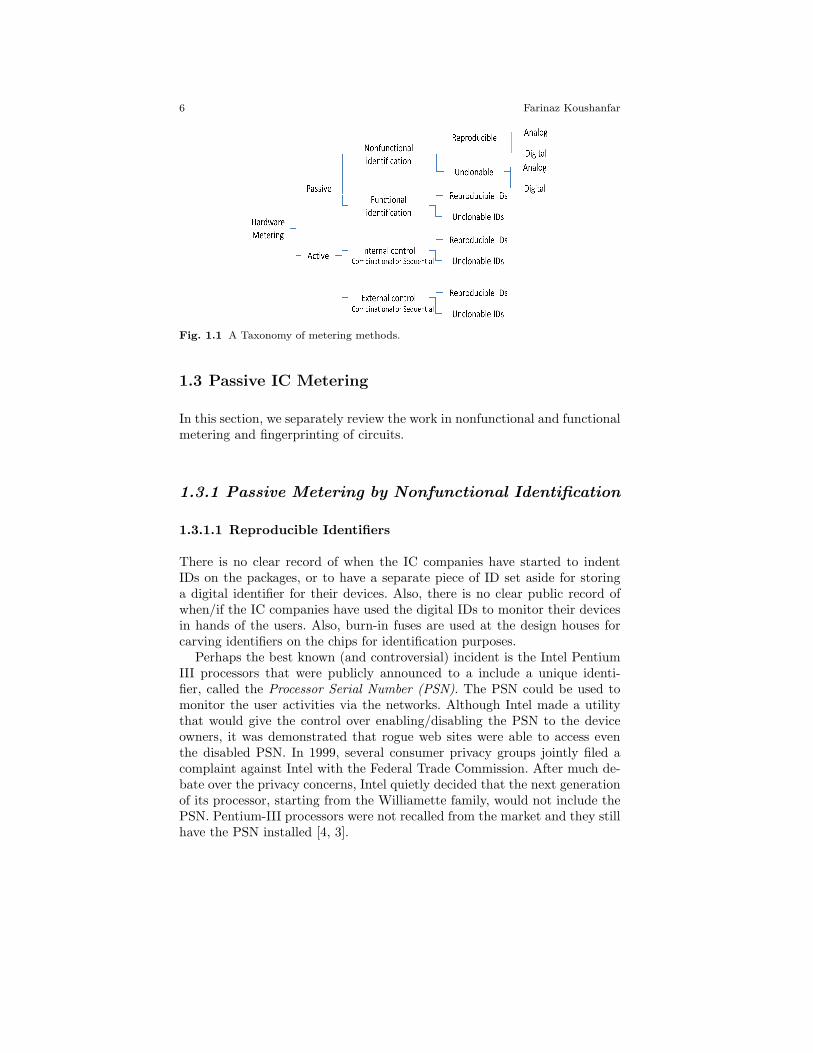
Figure 1.1 demonstrates a summary of the taxonomy described in thissection. Notice on the chart the distinction between the analog and digitalidentification for both reproducible and unclonable IDs. Although both ana-log and digital identification are possible, the existing methods for passivemetering based on functional identification and active metering (internal andexternal) all use the digital identifiers. This is because the digital IDs can bereadily integrated within the logical flow. In the remainder of the chapter,we focus on detailed description of the mechanisms and structures that havebeen proposed for passive and active metering.
6 Farinaz Koushanfar
Fig. 1.1 A Taxonomy of metering methods.
1.3 Passive IC Metering
In this section, we separately review the work in nonfunctional and functionalmetering and fingerprinting of circuits.
1.3.1 Passive Metering by Nonfunctional Identification
1.3.1.1 Reproducible Identifiers
There is no clear record of when the IC companies have started to indentIDs on the packages, or to have a separate piece of ID set aside for storinga digital identifier for their devices. Also, there is no clear public record ofwhen/if the IC companies have used the digital IDs to monitor their devicesin hands of the users. Also, burn-in fuses are used at the design houses forcarving identifiers on the chips for identification purposes.
Perhaps the best known (and controversial) incident is the Intel PentiumIII processors that were publicly announced to a include a unique identi-fier, called the Processor Serial Number (PSN). The PSN could be used tomonitor the user activities via the networks. Although Intel made a utilitythat would give the control over enabling/disabling the PSN to the deviceowners, it was demonstrated that rogue web sites were able to access eventhe disabled PSN. In 1999, several consumer privacy groups jointly filed acomplaint against Intel with the Federal Trade Commission. After much de-bate over the privacy concerns, Intel quietly decided that the next generationof its processor, starting from the Williamette family, would not include thePSN. Pentium-III processors were not recalled from the market and they stillhave the PSN installed [4, 3].

1 Hardware Metering: A Survey 7
As mentioned earlier, the drawback of indented IDs, digitally stored IDs,and burn-in fuses is that they can be tampered with, removed, or reproduced.As an example, a plausible and documented attack is repackaging of the oldertechnology as a new one. Digitally stored IDs and serial numbers can beoften read by noninvasive probing, and can be rewritten with a small effort.Also none of the available reproducible identification methods are able towithstand the foundry attack where the products are overbuilt. The foundrycan simply reproduce an ID by writing to the memory, or by reproducing thenumbers on the package.
1.3.1.2 Unclonable Identifiers
To overcome the limitations of the digital ID storage, methods for exploitingthe random process variations in silicon to generate a random unique iden-tifying (fingerprint) have been proposed. If exploiting the random processvariations is done by introducing a new circuit structure, this is an instanceof an extrinsic identification. If no new circuitry is introduced and only theexisting on chip components are used for identification, the method wouldbe an instance of an intrinsic identification. Note that the extrinsic/intrinsicdistinction also holds for FPGAs: if the contents of the FPGA (without re-configuring the cells) is used, then the identifiers are intrinsic. Any use ofreconfiguration of the devices would render the identification method an ex-trinsic one.Extrinsic methods. The earliest known instance of this class of work wasICID [28], where an an array of addressable transistors with common gateand source with sequentially selected drains was driving a resistive load. Thetransistors incurred threshold mismatches as a result of process variations.Therefore, the drain currents were randomly different, generating a sequenceof unique random numbers on the transistors. Several work in more sophis-ticated identification and authentication circuit methods has followed thisearly work, including the physical unclonable functions that were later intro-duced [13, 14]. Chapter 7 of this book has a thorough discussion on PUFs andon other unique objects based on the random physical disorder, including asystematic and new classification of the various work in this area.
In this chapter, we limit the discussion on the other methods that can beused for passive and active metering. It is also possible to make a distinctionbetween analog and digital extrinsic identifiers. For example, ICID generatesrandom bits that are in digital form, and can be potentially readily includedin a digital computation setting. It is plausible to design circuitry whoseanalog output depends on the underlying silicon process variations. Since formany applications it is desired to have digital outputs that can be readilyintegrated within the remainder of the digital design, most of the extrinsicID extraction circuitry have a digital response.

8 Farinaz Koushanfar
Intrinsic methods. The work in [13] has also proposed using the ICs’ timingpath signatures that are unique for each state-of-the-art CMOS chip (becauseof process variations) as a PUF. The interesting studies and new results in[8, 33] have shown that unique identification is possible for almost all ICsdesigned in state-of-the-art technology, as long as external test vectors canbe applied and structural (side channel) tests such as leakage, timing, anddynamic power measurements can be performed. This feature, allows identi-fication of all legacy ICs designed in technologies that contain manufacturingvariability, without adding any components to the chip. The requirementis that test measurement equipment for performing the structural tests isavailable and can be used.
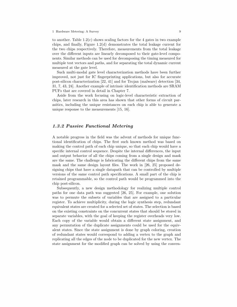
The proposed method in this latter work was based on the gate-level char-acterization of each IC that could be structurally tested. Since the character-ization is done nondestructively, there is no need for an additional circuitry.The extracted characteristics were continuous values, and multiple ways fordiscretizing and using the characteristics as unique chip IDs were suggested.Such nondestructive identification of legacy ICs can provide many oppor-tunities for creation of new IC metering and security protocols. The otherinteresting note about using the structural tests is that for a given number ofgates and their interconnections, there are many more test vectors, allowingone to generate an exponentially larger space of challenge-response pairs forone circuit. G1 G2 G3 G4i1i2 i3 i4 i5
(b)(a) (c) NAND2
Leakage (nA)Input
454.511
95.710
100.301
37.8400
NAND2
Leakage (nA)Input
454.511
95.710
100.301
37.8400
IC 2IC 1
0.93G4
42.1G3
0.61.3G2
2.40.5G1
Scaling factorGate
IC 2IC 1
0.93G4
42.1G3
0.61.3G2
2.40.5G1
Scaling factorGate
IC 2IC 1
1905184111001
2150124301110
1063208210101
2055139100011
Leakage (nA)Inputvector IC 2IC 1
1905184111001
2150124301110
1063208210101
2055139100011
Leakage (nA)Inputvector (d)
Fig. 1.2 (a) A design consisting of 4 NAND2 gates, (b) leakage current vs. input forNAND2,(c) scaling factors of gates on two ICs, and (d) total leakages of ICs for different
input vectors (source [8]).
Perhaps the best way to review the hidden characteristic extraction ap-proach is by showing an example (figure from [8]). In Figure 1.2(a) a smallcircuit consisting of four 2-input NAND gates. Table 1.2(b) shows the static(leakage) current of a nominal NAND2 for different possible inputs. However,because of process variations, the leakage current greatly varies from one chip
1 Hardware Metering: A Survey 9
to another. Table 1.2(c) shows scaling factors for the 4 gates in two examplechips, and finally, Figure 1.2(d) demonstrates the total leakage current forthe two chips respectively. Therefore, measurements from the total leakageover the different inputs are linearly decomposed to their gate-level compo-nents. Similar methods can be used for decomposing the timing measured formultiple test vectors and paths, and for separating the total dynamic currentmeasured at the gate level.
Such multi-modal gate level characterization methods have been furtherimproved, not just for IC fingerprinting applications, but also for accuratepost-silicon characterization [22, 41] and for Trojan (malware) detection [34,31, 7, 43, 24]. Another example of intrinsic identification methods are SRAMPUFs that are covered in detail in Chapter 7.
Aside from the work focusing on logic-level characteristic extraction ofchips, later research in this area has shown that other forms of circuit par-asitics, including the unique resistances on each chip is able to generate aunique response to the measurements [15, 16].
1.3.2 Passive Functional Metering
A notable progress in the field was the advent of methods for unique func-tional identification of chips. The first such known method was based onmaking the control path of each chip unique, so that each chip would have aspecific internal control sequence. Despite the internal differences, the inputand output behavior of all the chips coming from a single design and maskare the same. The challenge is fabricating the different chips from the samemask and the same design layout files. The work in [26, 25] proposed de-signing chips that have a single datapath that can be controlled by multipleversions of the same control path specifications. A small part of the chip isretained programmable, so the control path would be programmed into thechip post-silicon.
Subsequently, a new design methodology for realizing multiple controlpaths for one data path was suggested [26, 25]. For example, one solutionwas to permute the subsets of variables that are assigned to a particularregister. To achieve multiplicity, during the logic synthesis step, redundantequivalent states are created for a selected set of states. The selection is basedon the existing constraints on the concurrent states that should be stored inseparate variables, with the goal of keeping the register overheads very low.Each copy of the variable would obtain a different state assignment, andany permutation of the duplicate assignments could be used for the equiv-alent states. Since the state assignment is done by graph coloring, creationof redundant states would correspond to adding a vertex to the graph andreplicating all the edges of the node to be duplicated for the new vertex. Thestate assignment for the modified graph can be solved by using the conven-
10 Farinaz Koushanfar
tional graph coloring tools. Programmable read logic to the registers enablesselecting the correct permutation of the variables for each unique copy of thecontrol sequence.
1.3.2.1 Analysis of Passive Functional Metering
The passive metering protocol for detection of the unauthorized chips is tomonitor and evaluate the chips while they are in use. Before testing an au-thorized chip, the programmable part is loaded with a specific permutationof the control path. Now, if more than one copy of a single permutation isdetected, a counterfeit component is flagged. This protocol would work wellif many of the chips are online and can be queried for their permutation ver-sion of the internal control structure. One way to realize online querying isby XORing the states of the FFs to generate a checksum of the states, or byperforming other variants of integrity checking on the states.
One interesting scenario for passive metering is where the chips are re-turned unprogrammed to the designer who would enter the controller spec-ifications before testing the chips. The IP rights owner would ensure thateach of the chips are uniquely programmed and that the foundry is not in-volved in the programming step. However, this approach by itself does notstrongly deter the attackers, since an adversary with access to one unlockedchip can replicate the programmable memory’s content from one chip andthen use the information to configure and enable other chips. To avoid suchdirect replication attacks, the idea of integrating the programmable part withthe unclonable IDs coming from the chip was also suggested. At the time ofwriting the first passive hardware metering paper in 2000, the only knownunclonable identifiers where the ICIDs [28]. Therefore, the data for the pro-grammable part could not be replicated on other chips, naturally defendingagainst the overbuilding attacks.
The evaluation results in [26, 25] demonstrate that it is possible to obtainmultiple permutations and selection of the internal ordering of the controlsequences with a very low overhead. An obvious drawback of the presentedpassive metering approach is the overhead of adding the programmable partto ASICs, as this would require extra mask steps, incurring an additionalcost. Two probabilistic analysis were presented for the original passive me-tering method: (i) the first set of analysis answers the question of how manyexperiments should be conducted before one can conclude the absence ofunauthorized parts with a certain level of confidence; and (ii) the second setof analysis aims at estimating the number of unauthorized copies made, incase duplicate chips are detected on the market. Since these two analysismethods are generalizable to many other metering and unique identificationscenarios, in what follows we present the details of the analysis.
(i) Assume that the design house demands the foundry to fabricate n copies,but the foundry indeed fabricates N chips where N >> n. If the company

1 Hardware Metering: A Survey 11
makes k− 1 copies of each, the total number of available ICs from the designwould be:N = kn. Note that it is proven that the foundry has the best chanceof not getting detected by fabricating equal number of copies of each chip. Ifwe draw l from the N objects consisting of k copies of distinct designs, theprobability of no duplicate would be:
Prob[n, k, l] = [1− k − 1
N − 1].[1− 2(k − 1)
N − 2] . . . [1− (l − 1)(k − 1)
N − l − l], (1.1)
that is upper bounded by:
Prob[n, k, l] ≤ [1− p
n].[1− 2p
n] . . . [1− (l − 1).p
n], (1.2)
where p = 1− 1k . As can be seen above, as the value of k increases, the prob-
ability Prob[n, k, l] of not finding unauthorized parts after l random tests(without replacement) decreases. The probability Prob[n, k, l] decreases asthe number of tests l, increases. In essence, the quantity 1 − Prob[n, k, l]measures the foundry’s honesty and it increases as l increases. For a designerto obtain a desired level of confidence α, one need to find the smallest l suchthat (1 − Prob[n, k, l]) ≥ α. Since finding an exact closed form formula forEquation 1.1 is challenging, the solution is often found by numerical estima-tions or by using approximations in case of large n.
(ii) Assuming that k is uniformly distributed, one can immediately find theprobability that the first unauthorized copy is found at the l + 1-th test as:
Prob[n, k, l + 1] = Prob[n, k, l].l.(l − 1).(k − 1)
N − 1. (1.3)
The expected number of tests to find the first unauthorized copy would be:
inf∑k=1
n(k−1)+1∑l=1
l.P rob[n, k, l], (1.4)
and if the first failure occurs at l, then the expectation for k is:
E[k] =inf∑k=1
k.Prob[n, k, l]. (1.5)
1.4 Active IC Metering
Active hardware metering not only uniquely and unclonably identifies eachchip, but also provides an active mechanism to control, monitor, lock, orunlock the ICs post fabrication. To ensure irreproducibility, active meter-
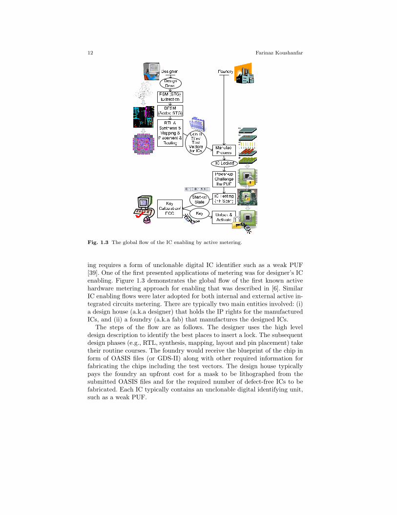
12 Farinaz KoushanfarDesigner FoundryDesign Desc.FSM (STG)ExtractionBFSM (Added STG) IC Locked Key Calculation/ECC Unlock & Activate
GDS II Files/ Test Vectors for ICsStart-up StateKey
Manufac.ProcessRTL &Synthesis &Mapping &Placement &RoutingIC Testing(FF Scan)0 1 0 0 1 1 1 0 Power-upChallenge the PUF
Fig. 1.3 The global flow of the IC enabling by active metering.
ing requires a form of unclonable digital IC identifier such as a weak PUF[39]. One of the first presented applications of metering was for designer’s ICenabling. Figure 1.3 demonstrates the global flow of the first known activehardware metering approach for enabling that was described in [6]. SimilarIC enabling flows were later adopted for both internal and external active in-tegrated circuits metering. There are typically two main entities involved: (i)a design house (a.k.a designer) that holds the IP rights for the manufacturedICs, and (ii) a foundry (a.k.a fab) that manufactures the designed ICs.
The steps of the flow are as follows. The designer uses the high leveldesign description to identify the best places to insert a lock. The subsequentdesign phases (e.g., RTL, synthesis, mapping, layout and pin placement) taketheir routine courses. The foundry would receive the blueprint of the chip inform of OASIS files (or GDS-II) along with other required information forfabricating the chips including the test vectors. The design house typicallypays the foundry an upfront cost for a mask to be lithographed from thesubmitted OASIS files and for the required number of defect-free ICs to befabricated. Each IC typically contains an unclonable digital identifying unit,such as a weak PUF.
1 Hardware Metering: A Survey 13
Building a mask is a costly and complex process, involving multiple finesteps that should be closely controlled [30, 40]. Once the foundry lithographsa mask, multiple ICs would be fabricated from this mask. Because of thespecific PUF responses integrated within the locks on the chips, each ICwould be uniquely locked (nonfunctional) upon fabrication. During a start-uptest phase, the fab scans the unique identifier information out of each IC andsends the content back to the design house. The design house that uses thedesigner-specific knowledge or an asymmetric cryptography protocol, is theonly entity who could compute the unlocking sequence for each locked chip.Additionally, the designer could compute the error correcting code (ECC)to correct for any further changes to the unclonable digital identifiers. TheECC is very important since a few of PUF response bits may be unstableand change at a later time because of noise, environmental conditions (e.g.,temperature), or circuit instability. The key for unlocking the chip and theECC would then be sent back to the fab.
The work in [6, 9] have also discussed methods such that the designer’sasymmetric information about parts of the design could be utilized for othercontrol purposes, including but not limited to online enabling/disabling andcontinuous authentication.
1.4.1 Internal (Integrated) Active IC Metering
The first set of introduced methods for metering were internal [6]. The ac-tive IC control mechanism in this class of work leverages: (i) the functionaldescription of the design, and (ii) unique and unclonable IC identifiers. Thelocks are embedded within the structure of the common computation modelin hardware design, in form of a finite state machine (FSM). The designer ex-ploits the high level design description to form the designs behavioral modelin the FSM format. FSM is typically represented by the State TransitionGraph (STG) where the vertices on the graph correspond to the states inthe FSM, and the transitions between the FSM states are represented by thedirected edges incident to the vertices. In the remainder of this chapter, weuse the terms FSM and STG interchangeably. Let us describe the approachin [6]. We use the term original FSM to refer to the design’s finite statemachine before modifications (with |S| states). Therefore, the original FSMcould be implemented using K = log|S| FFs.
Now assume that we modify the original FSM by augmenting to its statesand transitions. We call the modified design a boosted finite state machine(BFSM). To build a BFSM with |S′| + |S| states, we would require K” =log{|S′| + |S|} FFs. Additional edges are also introduced to the BFSM toensure the reachability of its states. Observe that for a linear growth in thenumber of FFs denoted by K ′ = K”−K, the number of states exponentiallyincreases. Indeed, by adding a number of FFs and tolerating the overhead of
14 Farinaz Koushanfar
this addition, it is possible to set S′ >> S so that the number of new statesare exponentially many more than |S|.
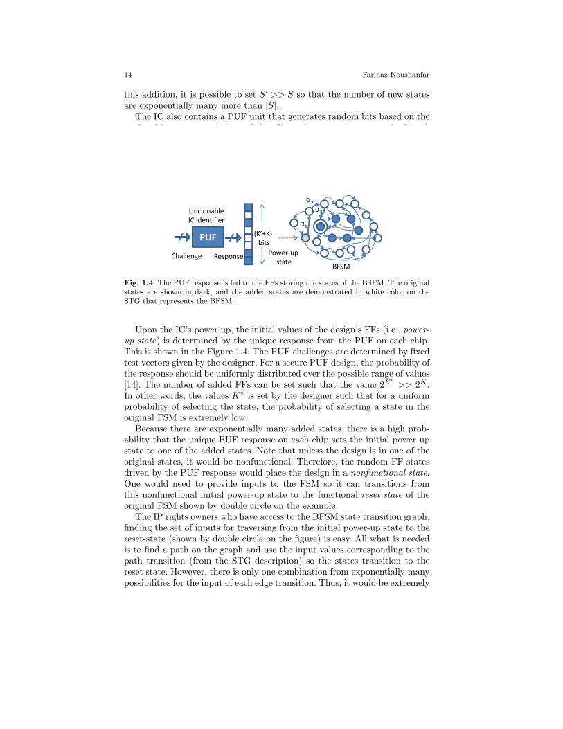
The IC also contains a PUF unit that generates random bits based on theunclonable process variations of the silicon that are unique on each chip. Afixed challenge is applied to the chip upon power up. The PUF response is fedto the FFs that implement the BFSM. Since there are K” = log{|S′|+ |S|}FFs in the BFSM, one would need K” response bits from the PUF for aproper operation.
PUF(K’+K)
bits
ResponseChallenge Power-up
stateBFSM
α1
α2
α3Unclonable
IC Identifier
Fig. 1.4 The PUF response is fed to the FFs storing the states of the BSFM. The original
states are shown in dark, and the added states are demonstrated in white color on theSTG that represents the BFSM.
Upon the IC’s power up, the initial values of the design’s FFs (i.e., power-up state) is determined by the unique response from the PUF on each chip.This is shown in the Figure 1.4. The PUF challenges are determined by fixedtest vectors given by the designer. For a secure PUF design, the probability ofthe response should be uniformly distributed over the possible range of values[14]. The number of added FFs can be set such that the value 2K” >> 2K .In other words, the values K” is set by the designer such that for a uniformprobability of selecting the state, the probability of selecting a state in theoriginal FSM is extremely low.
Because there are exponentially many added states, there is a high prob-ability that the unique PUF response on each chip sets the initial power upstate to one of the added states. Note that unless the design is in one of theoriginal states, it would be nonfunctional. Therefore, the random FF statesdriven by the PUF response would place the design in a nonfunctional state.One would need to provide inputs to the FSM so it can transitions fromthis nonfunctional initial power-up state to the functional reset state of theoriginal FSM shown by double circle on the example.
The IP rights owners who have access to the BFSM state transition graph,finding the set of inputs for traversing from the initial power-up state to thereset-state (shown by double circle on the figure) is easy. All what is neededis to find a path on the graph and use the input values corresponding to thepath transition (from the STG description) so the states transition to thereset state. However, there is only one combination from exponentially manypossibilities for the input of each edge transition. Thus, it would be extremely
1 Hardware Metering: A Survey 15
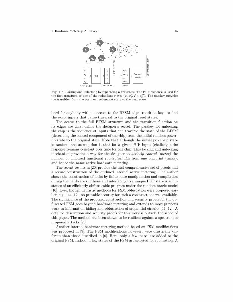
Fig. 1.5 Locking and unlocking by replicating a few states. The PUF response is used forthe first transition to one of the redundant states (q3, q′3, q”3, q
′′′3 ). The passkey provides
the transition from the pertinent redundant state to the next state.
hard for anybody without access to the BFSM edge transition keys to findthe exact inputs that cause traversal to the original reset states.
The access to the full BFSM structure and the transition function onits edges are what define the designer’s secret. The passkey for unlockingthe chip is the sequence of inputs that can traverse the state of the BFSM(describing the control component of the chip) from the initial random power-up state to the original state. Note that although the initial power-up stateis random, the assumption is that for a given PUF input (challenge) theresponse remains constant over time for one chip. This locking and unlockingmechanism provides a way for the designer to actively control (meter) thenumber of unlocked functional (activated) ICs from one blueprint (mask),and hence the name active hardware metering.
The recent results in [20] provide the first comprehensive set of proofs anda secure construction of the outlined internal active metering. The authorshows the construction of locks by finite state manipulation and compilationduring the hardware synthesis and interfacing to a unique PUF state is an in-stance of an efficiently obfuscatable program under the random oracle model[10]. Even though heuristic methods for FSM obfuscation were proposed ear-lier, e.g., [44, 12], no provable security for such a constructions was available.The significance of the proposed construction and security proofs for the ob-fuscated FSM goes beyond hardware metering and extends to most previouswork in information hiding and obfuscation of sequential circuits [44, 12]. Adetailed description and security proofs for this work is outside the scope ofthis paper. The method has been shown to be resilient against a spectrum ofproposed attacks [20].
Another internal hardware metering method based on FSM modificationswas proposed in [9]. The FSM modifications however, were drastically dif-ferent than those described in [6]. Here, only a few states are added to theoriginal FSM. Indeed, a few states of the FSM are selected for replication. A

16 Farinaz Koushanfar
replicated state q′i (i.e., a copy of an original state qi) is an added state to thegraph such that all the incident edges from/to the neighbors of qi are copiedto the state q′i. Different passkeys are associated with the original edges andthe replicated edges. The locking is performed such that only one of qi or q
′i
are selected for each chip by the random unique IDs of that chip. The ID canbe scanned out from the chip. The provided input for edge transitions to andfrom the selected state is the one passkey that can perform unlocking.
An example for this operation is demonstrated in Figure 1.5. One the fig-ure, the overall schematic for an FSM with a lock on the replicated state (q3on the example) is demonstrated. Three replications of the state q3, denotedby q′3, q
′′3 , and q′′′3 are shown for the sake of the example. The response from
the PUF determines the transition edge to one of the redundant states (ei-ther q3 or one of its replicates). The response is also XOR’d with the passkey(computed by the original designer) to provide the transition out of the re-dundant state. Without the passkey, the transition will not take place orwill be incorrect with a very high probability. Note that in real settings, thekey length should be properly selected to thwart the brute-force attacks andguarantee security by point function. The significance of this new structureis that the locks are embedded within the internal states that are also visitedduring the IC’s normal operation. Therefore, the locks and keys are contin-ually accessed during the IC’s normal operation, creating an opportunity forcontinuous authentication and self checking.
It is interesting to note that FSM-based hardware metering method canbe also used in the context of third party IP integration, where each of theIP cores on a chip can be enabled, disabled, or otherwise controlled [5]. Inthis approach, a designer or an integrator is the reuser of existing third partyIP cores. Two other entities involved in this design and reuse protocol modelare the fabrication plant and an authorized system verifier, referred to as acertificate authority (CA). This latter entity a trusted third party who ensuresa trust between hardware IP providers, reusers, and the fab.
Let us consider a scenario where multiple third party core blocks are tobe protected. Each IP block contains a lock in its FSM structure. The resuerincludes also two new modules in the design, the unclonable identificationcircuitry, and an embedded control module. The embedded control moduleinteracts with and controls the various locks inside each third-party IP block.The blueprint of the design is sent to the CA before sending to fabrication.The CA certifies the IP core providers and the reuser. The post-silicon chipsare tested for their unclonable IDs that are sent back to the CA. The CAcontacts the third party IP providers and the reuser to get the passkeys forthe IP block cores and the embedded control module. Note that similar thirdparty IP protection models can be applied to cases where external activehardware metering is used for locking each core.

1 Hardware Metering: A Survey 17
1.4.2 External Active IC Metering
External active IC metering methods lock every IC by asymmetric crypto-graphic techniques that require a specific external key. The use of asymmetriccryptography for external IC metering was first proposed by EPIC [37]. SinceEPIC has been a basis for most of the subsequent work in external activemetering, we discuss this methodology in detail.
To support Public Key Cryptography (PKC), the IP rights holder mustgenerate a pair of master keys (MKs) (public and private) that will remainunaltered. The private master key (MK-Pri) embodies IP rights for a givendesign and is never transmitted. Each fabricated chip produces its own ran-dom public and private key pairs upon start-up. Also embedded in the registertransfer level (RTL) are the public master key (MK-Pub) and the minimalcircuitry to support the EPIC’s combinational locking mechanism.
EPIC implements combinational locking in the chip’s main modules byadding XOR gates on a number of selected noncritical wires, with addedcontrol signals connected to the common key (CK) register. When the cor-rect CK is present, the circuit is equivalent to the original; otherwise, thechip’s behavior is changed, as if stray inverters were located on selected wires.EPIC produces the CK at random to prevent it from being stolen earlier. Af-ter modifying the placed design, the designer securely communicates the CKto the IP rights holder and erases all other copies. Routing and other physi-cal optimizations then proceed as normal, followed by manufacturing. Uponmanufacturing, each IC will be uniquely locked because of the interface withthe random and unclonable IDs generated by the IC.
While activating a chip, the foundry must have a secure link with thedesigner (IP rights holder) and must send the RCK-Pub for the IC to beactivated. EPIC’s protocol uses the foundry’s private key to authenticatethe transmission. Extensions to this protocol may send a time stamp, serialnumber, or other identifying sequences. In response, the designer (IP rightsholder) transmits the input key (IK) that shows the CK encrypted with thePCK-Pub and signed by the MK-Pri afterwards. The ordering of encryptionand signing of the CK for generating the IK is crucial so that entities otherthan the designer (IP rights holder) cannot produce IKs, even if the CK iscompromised. Using the RCK-Pub to encrypt the messages makes statisticalattacks against the MK-Pri more complex. The designer can use the foundry’spublic key to additionally encrypt the resulting IK so that only the manufac-turer can receive it. The IC decrypts the IK using the RCK-Pri and MK-Pubthat authenticate it as being sent by the designer. Upon decryption, the CKis generated that unlocks the chip and facilitates testing. After the testingstep, the IC can be sold.
EPIC is shown to be resilient against a number of proposed attacks, asdescribed in [38]. Note that an early version of EPIC was evaluated by otherresearchers in terms of security and overhead [29]. They found that EPIC isvulnerable if the IK is calculated from the CK, MK-Pri, and RCK-Pub in the
18 Farinaz Koushanfar
wrong order; the CK must first be encrypted with the PCK-Pub and thenthe resultant ciphertext must be signed by the MK-Pri that is a standardprotocol for public-key communication with nonrepudiation. On the otherhand, if the IK is computed properly, no successful logic-level attacks againstEPIC are known. These issues were discussed and fully addressed in the latestversion of EPIC [38].
[36] presented an external IC locking method built upon secret sharing.The chip and the design plant share a secret key that is interfaced with thecombinational logic on the circuit and is used for locking and controlling ofthe buses that can be used to connect and interface the multiple cores on onechip.
[18] proposed an active IC metering approach that shared many of theideas, protocols, and methods developed by EPIC. The work presented dif-ferent design choices and an example on how to implement the protectionscheme in resource-constrained environment. The low overhead approach wastargeted to both device authentication and user authentication.
[11] introduced another combinational locking method that like [26, 25]utilizes a small programmable part within the chip, that is referred to byreconfigurable logic barriers. However, unlike the earlier work that used theprogrammable parts for passive metering, the reconfigurable logic barriers in[11] were used for active metering. [11] decomposes the IP functionality F (x)into Ffixed and Freconfig. The idea is to protect the design by not disclosingthe Freconfig to the fabrication plant. The withheld Freconfig partition isprogrammed into the reconfigurable locations during the activation stageusing a secure key distribution. The suggestion combinational locking methodis a mix of XORs (similar to [37]) and k-input lookup tables (LUTs). Aselection heuristic was proposed to optimize the lock placement. The heuristicis aimed at making a barrier for the logic transition, such that the signalswould not traverse to the output without passing through the locks. Exceptfor heuristic methods, no security guarantee was provided by this work.
As mentioned earlier, the advantage of such programmable parts is keepinga part of the design to the IP rights holder. The drawback is the added processand mask overhead incurred for implementing the programmable componentswithin ASIC. For more technical details, we refer the interested readers tothe published papers on the external active metering subject, including [18,37, 36, 38, 11].
1.5 Conclusions
This chapter provided a comprehensive overview of hardware integrated cir-cuits (IC) protection by metering. IC metering refers to mechanisms, methodsand protocols that enable tracking of the chips post-silicon. IC metering ismotivated by the increased rate of outsourcing of leading-edge chip fabri-

1 Hardware Metering: A Survey 19
cation to offshore foundries that creates opportunities for overbuilding andpiracy. IC metering helps the designers to identify and/or track their designspost-fabrication. In our new taxonomy, hardware metering was divided intotwo categories: passive and active. Passive metering either assigns an iden-tifier to the chip (which maybe reproducible or unclonable), or it assigns asignature to the internals of an IC, while the chip maintains its functionalityand integrity. One interesting aspect of passive metering is that it is pos-sible to uniquely monitor and track legacy ICs without the need for addedcircuitry by exploiting the inherent variations in silicon. In active metering,not only the ICs are uniquely identified, but also parts of the chip’s function-ality can be only accessed, locked (disabled), or unclocked (enabled) by thedesigner. We discussed both internal and external active hardware metering.Overall, the hope is that by limiting the opportunities for piracy and theft ofICs using post-silicon control mechanisms and protocols, hardware meteringwould be able to directly and significantly improve the business and practiceof semiconductor design and manufacturing.
References
1. Defense science board (DSB) study on high performance microchip supply.http://www.acq.osd.mil/dsb/reports/2005-02-hpms report final.pdf.
2. Managing the risks of counterfeiting in the information technology industry. a white
paper by kpmg and the alliance for gray market and counterfeit abatement (agma).3. Pentium III serial numbers, http://www.pcmech.com/article/pentium-iii-serial-
numbers/.4. Pentium III wikipedia page, http://en.wikipedia.org/wiki/pentium iii.
5. Y. Alkabani and F. Koushanfar. Active control and digital rights management ofintegrated circuit IP cores. In International Conference on Compilers, Architecture,and Synthesis for Embedded Systems (CASES), 2007.
6. Y. Alkabani and F. Koushanfar. Active hardware metering for intellectual propertyprotection and security. In USENIX Security Symp., pages 291–306, 2007.
7. Y. Alkabani and F. Koushanfar. Consistency-based characterization for IC Trojandetection. In International Conference on Computer Aided Designs (ICCAD), pages
123–127, 2009.8. Y. Alkabani, F. Koushanfar, N. Kiyavash, and M. Potkonjak. Trusted integrated
circuits: A nondestructive hidden characteristics extraction approach. In InformationHiding conference (IH), pages 102–117. Springer, 2008.
9. Y. Alkabani, F. Koushanfar, and M. Potkonjak. Remote activation of ICs forpiracy prevention and digital right management. In The International Conferenceon Computer-Aided Design (ICCAD), 2007.
10. B. Barak, O. Goldreich, R. Impagliazzo, S. Rudich, A. Sahai, S. Vadhan, and
K. Yang. On the (im)possibility of obfuscating programs. In Advances in Cryptology(CRYPTO), pages 1–18, 2001.
11. A. Baumgarten, A. Tyagi, and J. Zambreno. Preventing IC piracy using reconfigurablelogic barriers. IEEE Design & Test of Computers, 27:66–75, 2010.
12. R. Chakraborty and S. Bhunia. Hardware protection and authentication throughnetlist level obfuscation. In The International Conference on Computer-Aided Design(ICCAD), pages 674–677, 2008.

20 Farinaz Koushanfar
13. S. Devadas and B. Gassend. Authentication of integrated circuits. US Patent 7,840,803,
2010. Application in 2002.14. B. Gassend, D. Clarke, M. van Dijk, and S. Devadas. Silicon physical random functions.
In CCS, pages 148–160, 2002.15. R. Helinski, D. Acharyya, and J. Plusquellic. A physical unclonable function defined
using power distribution system equivalent resistance variations. In Design Automa-tion Conference (DAC), pages 676–681, 2009.
16. R. Helinski, D. Acharyya, and J. Plusquellic. Quality metric evaluation of a physi-cal unclonable function derived from an IC’s power distribution system. In Design
Automation Conference, DAC, pages 240–243, 2010.17. D. Holcomb, W. Burleson, and K. Fu. Power-up SRAM state as an identifying fin-
gerprint and source of true random numbers. IEEE Transactions on Computers,58(9):1198–1210, September 2009.
18. J. Huang and J. Lach. IC activation and user authentication for security-sensitive sys-tems. In International Symposium on Hardware-Oriented Security and Trust (HOST),pages 76–80, 2008.
19. D. Kirovski and M. Potkonjak. Localized watermarking: methodology and applicationto operation scheduling. In The International Conference on Computer-Aided Design(ICCAD), pages 596–599, 1999.
20. F. Koushanfar. Active integrated circuits metering techniques for piracy avoidance and
digital rights management. Technical Report TREE1101, ECE Dept., Rice University,2011.
21. F. Koushanfar and Y. Alkabani. Provably secure obfuscation of diverse watermarksfor sequential circuits. In International Symposium on Hardware-Oriented Security
and Trust (HOST), pages 42–47, 2010.22. F. Koushanfar, P. Boufounos, and D. Shamsi. Post-silicon timing characterization
by compressed sensing. In The International Conference on Computer-Aided Design(ICCAD), pages 185–189, 2008.
23. F. Koushanfar, I. Hong, and M. Potkonjak. Behavioral synthesis techniques for intel-lectual property protection. ACM Transactions on Design Automation of ElectronicSystems (TODAES), 10(3):523–545, 2005.
24. F. Koushanfar and A. Mirhoseini. A unified submodular framework for multimodal IC
trojan detection. IEEE Transactions on Information Forensics and Security (TIFS),to appear, 2011.
25. F. Koushanfar and G. Qu. Hardware metering. In Design Automation Conference
(DAC), Design Automation Conference (DAC), pages 490–493, 2001.26. F. Koushanfar, G. Qu, and M. Potkonjak. Intellectual property metering. In Interna-
tional Workshop on Information Hiding (IHW), pages 81–95. Springer, 2001.27. J. Lach, W. Mangione-Smith, and M. Potkonjak. Signature hiding techniques
for FPGA intellectual property protection. In The International Conference onComputer-Aided Design (ICCAD), pages 186–189, 1998.
28. K. Lofstrom, W. R. Daasch, and D. Taylor. IC identification circuit using devicemismatch. In International Solid-State Circuits Conference (ISSCC), pages 372–373,
2000.29. R. Maes, D. Schellekens, P. Tuyls, and I. Verbauwhede. Analysis and design of active
IC metering schemes. In International Symposium on Hardware-Oriented Securityand Trust (HOST), pages 74–81, 2009.
30. C. Mouli and W. Carriker. Future fab: How software is helping intel go nano–andbeyond. IEEE Spectrum, March 2007.
31. M. Nelson, A. Nahapetian, F. Koushanfar, and M. Potkonjak. SVD-based ghost cir-cuitry detection. In IH, pages 221–234, 2009.
32. A. Oliveira. Techniques for the creation of digital watermarks in sequential circuitdesigns. IEEE Transactions on. Computer-Aided Design of Integrated Circuits andSystems (TCAD), 20(9):1101–1117, 2001.

1 Hardware Metering: A Survey 21
33. M. Potkonjak and F. Koushanfar. Identification of integrated circuits. US Patent
Application 12/463,984; Publication Number: US 2010/0287604 A1, May 2009.34. M. Potkonjak, A. Nahapetian, M. Nelson, and T. Massey. Hardware Trojan horse
detection using gate-level characterization. In Design Automation Conference (DAC),pages 688–693, 2009.
35. G. Qu and M. Potkonjak. Intellectual Property Protection in VLSI Design. Springer,2003.
36. J. Roy, F. Koushanfar, and I. Markov. Protecting bus-based hardware IP by secretsharing. In Design Automation Conference (DAC), pages 846–851, 2008.
37. J. Roy, F. Koushanfar, and I. Markov. EPIC: Ending piracy of integrated circuits. InDesign Automation and Test in Europe (DATE), pages 1069–1074, 2008.
38. J. Roy, F. Koushanfar, and I. Markov. Ending piracy of integrated circuits. IEEEComputer, 43:30–38, 2010.
39. U. Ruhrmair, S. Devadas, and F. Koushanfar. Book Chapter in Introduction to Hard-ware Security and Trust, M. Tehranipoor and C. Wang editors, chapter 7: Securitybased on Physical Unclonability and Disorder. Springer, 2011.
40. B. Santo. Plans for next-gen chips imperiled. IEEE Spectrum, August 2007.41. D. Shamsi, P. Boufounos, and F. Koushanfar. Noninvasive leakage power tomography
of integrated circuits by compressive sensing. In International Symposium on LowPower Electronic Design (ISLPED), pages 341–346, 2008.
42. I. Torunoglu and E. Charbon. Watermarking-based copyright protection of sequentialfunctions. IEEE Journal of Solid-State Circuits (JSSC), 35(3):434–440, 2000.
43. S. Wei, S. Meguerdichian, and M. Potkonjak. Gate-level characterization: Foundationsand hardware security applications. In Design Automation Conference (DAC), 2010.
44. L. Yuan and G. Qu. Information hiding in finite state machine. In Information HidingConference (IH), pages 340–354. Springer, 2004.