Embed Size (px)
Citation preview

1

AN ABSTRACT OF THE DISSERTATION OF
Pavan Kumar Hanumolu for the degree of Doctor of Philosophy in
Electrical and Computer Engineering presented on August 21, 2006.
Title: Design Techniques for Clocking High Performance Signaling Systems.
Abstract approved:
Un-Ku Moon
Scaling of CMOS technology has progressed relentlessly for the past several
decades. In order for this unprecedented scaling to benefit the performance of
large digital systems, the communication bandwidth between integrated circuits
(ICs) must scale accordingly. However, interconnect technology does not scale as
aggressively, making communication between chips the major bottleneck in overall
system performance. In addition, supply voltage scaling, increasing device leakage,
and increased noise make existing signaling circuits inefficient and difficult to scale.
In this thesis, both analog and digital enhancement techniques to mitigate
scaling related issues and improve the performance of building blocks used in high-
speed signaling systems are discussed. A digital-to-phase converter (DPC) with a
resolution better than 100 femto-second resolution, a hybrid analog/digital clock
and data recovery (CDR) architecture that improves the tracking range of tra-
ditional CDRs by an order of magnitude, and a digital CDR architecture that
obviates the need for the charge pump and the large area occupying loop filter,
while achieving error-free operation are presented. Measured results obtained from
the prototype chips are presented to illustrate the proposed design techniques.

c©Copyright by Pavan Kumar Hanumolu
August 21, 2006
All Rights Reserved
Design Techniques for Clocking High Performance Signaling Systems
by
Pavan Kumar Hanumolu
A DISSERTATION
submitted to
Oregon State University
in partial fulfillment ofthe requirements for the
degree of
Doctor of Philosophy
Presented August 21, 2006Commencement June 2007

Doctor of Philosophy dissertation of Pavan Kumar Hanumolu presented on
August 21, 2006
APPROVED:
Major Professor, representing Electrical and Computer Engineering
Director of the School of Electrical Engineering and Computer Science
Dean of the Graduate School
I understand that my dissertation will become part of the permanent collection
of Oregon State University libraries. My signature below authorizes release of my
dissertation to any reader upon request.
Pavan Kumar Hanumolu, Author
ACKNOWLEDGMENTS
Pursuing a doctoral degree is like venturing into a long journey imbued with
both intellectual spirit and capricious blend of uncertainties. I for one have thor-
oughly enjoyed this thrill-a-minute endeavor for all of the last five years. At the
end of it all, I feel that there is as much pleasure in the journey as there is in
reaching the destination. For that, I would like to thank all the people who made
at times turbulent journey a pleasant experience and helped me reach the summit
which looked hopelessly insurmountable at various stages.
First and foremost, I am deeply indebted to my peerless advisor Professor
Un-Ku Moon, for giving me the golden opportunity of being part of his group
when I knew little about circuits. He gave me the freedom and provided all the
means, financial and otherwise, to pursue my own ideas and showed seemingly
unlimited patience when I frequently digressed into other areas of his research. He
is also a circuit designer of transcendental brilliance and I greatly benefited from
his expertise. He will be a role model that I will look up to as I start my career in
academia.
Professor Gu-Yeon Wei of Harvard University unselfishly agreed to be my co-
advisor despite being 3000 miles away and generously shared his vast knowledge
on links design. Gu masterfully explained the nitty-gritty of my own designs with
consummate ease and frequently improved them by way of suggesting changes that
were certainly beyond my scope of thinking. He also laboriously edited my papers
and presentations and trained me on how to give good talks. I am grateful for his
tutelage and look forward to the continued friendship and collaboration.
Randy Mooney of Intel Circuit Research Labs introduced me to serial links
and then provided both financial and intellectual support for all of my research

on this topic. In spite of his busy schedules, he always found time to listen to
my ideas, good and mostly bad, and provided invaluable feedback. He gave me
the best advice regardless of the consequences for him. I am deeply indebted
to him for his generosity, kindness, and guidance. I also greatly benefited from
the interactions with all the members of his research team, past and present:
Ganesh Balamurugan, Bryan Casper, David Johnson, James Jaussi, Joe Kennedy,
Mozghan Mansuri, Aaron Martin, and Frank O’mahoney. In particular, Aaron,
Bryan, and David answered all my questions very patiently when I first started
this work. I am grateful for all their help. I would also like to thank Matt Haycock
and Shekar Borkar for constant encouragement and support.
I am indebted to the mighty Professor Temes for his invaluable advice on
both technical and personal matters. He has been a source of inspiration all along
and I feel fortunate and honored to have had the opportunity to interact with
him. I would be remiss if I do not mention how thoroughly I enjoyed his stories
that were generously filled with humor, wit, and inspiration. I also appreciate the
kindness of Professor Temes and Ibi for inviting me to their home for excellent
dinners.
Professor Mayaram rigorously edited my writing and taught me technical
writing style by example. He also provided unconditional help and precious advice
through out my graduate study and I am deeply grateful to him for that.
I would also like to thank Professor Solomon Yim for serving on my commit-
tee. Thanks are also due to Merrick Brownlee, Rob Gregoire, and Sunwoo Kwon
for reading my thesis and providing feedback.
Andy, Clara, Josh, Morgan, Nancy, and Sarah worked relentlessly to put
bureaucracy at bay and made sure the much needed checks came in on time.
Ferne has a next to impossible and often thankless job of assisting all the ECE
graduate students. But, she some how tactfully manages to help everybody with
unlimited patience, grace, and cordiality. I am also grateful to Manfred Dittrich
for his help with my test setup preparations. Thank you for all your help and
friendship.
My tenure as a graduate student in Corvallis would’nt have been as enjoy-
able and as fulfilling without the support of my beloved friends. I am not eloquent
enough to adequately express my true feelings of joy and gratitude for their friend-
ship. Nevertheless, I would like to acknowledge them. Gil-cho Ahn taught me not
to take anything for granted, particularly good things in life. Matt Brown, Jose
Silva, and Jose Ceballos showed great concern for my well-being, much more than a
good friend could or should ask for. Merrick Brownlee, Volodymyr Kratyuk (a.k.a
Vova), and Todd Shechter often performed wizardry with computers and saved me
from insanity! Min Gyu Kim showed me the value of simplicity both in circuit
design and in life. Arun Rao did the best favor I could ask of him by introducing
me to Professor Moon and Dong-Young Chang made me feel at home when I first
came to Corvallis. Thank you all for your unconditional support at all times.
Daily coffee breaks and weekly dinner meetings at Bombs Away with my best
buddies Amy Doty, Erik Geissenhainer, Christopher Hanken, Wonseok Huang,
Celia Hung, Min Gyu Kim, Sunwoo Kwon, Jim Le, Nema Talebbeydokhti, and
Eric Vernon served as perfect tools for stress relief. You made bad times seem not
that bad and work seem less work. Thank you for your friendship.
I also greatly enjoyed the good company and camaraderie of Anurag, David
B., Dave G., Emma, Gowtham, Jack, Jake, James, Josh, Jipeng, Kerem, Kye-
hyung, Martin, Nag, Nishanth, Peter, Rob, Robert, Ruopong, Sasidhar, Tawfiq,
Ting, Thuy, Wonseok, Xuesheng, Younjae, and Zhenyong. If I inadvertently forgot
anybody, I ask you as a good friend to forgive my ungratefulness! I will forever

cherish the good times we all had together.
The couples Charlie/Meridith, Jose/Marcella, Min Gyu/Suk-Hyeon, Matt/Melinda,
and Vova/Miroslava invited me for sumptuous dinners on numerous occasions,
something, as a starving graduate student, I always longed for.
I am grateful to Samsung Electronics and National Semiconductor for provid-
ing the fabrication of my test chips. In particular, I would like to thank Sang-Hyeon
Lee, Amjad Obeidat, Kim Yeow Wong, and Bijoy Chatterjee for their herculean
efforts to make the fabrication possible.
Finally, but immensely, I would like to thank my parents for teaching me the
true value of education and continued learning. My deepest gratitude belongs to
them for their sacrifice, love, and support. I would also to thank my brother for
his love and friendship. This thesis for all its worth is dedicated to them.

TABLE OF CONTENTS
Page
1. INTRODUCTION . . . . . . . . . . . . . . . . . . . . . . . . . . . . . . . . . . . . . . . . . . . . . . . . . . . 1
1.1 Channel Loss . . . . . . . . . . . . . . . . . . . . . . . . . . . . . . . . . . . . . . . . . . . . . . . . . . . . 2
1.2 Clock Jitter . . . . . . . . . . . . . . . . . . . . . . . . . . . . . . . . . . . . . . . . . . . . . . . . . . . . . . 5
1.3 Thesis Organization. . . . . . . . . . . . . . . . . . . . . . . . . . . . . . . . . . . . . . . . . . . . . . 6
2. PERFORMANCE ANALYSIS METHODS FOR SERIAL LINKS . . . . . 8
2.1 Worst Case ISI Analysis . . . . . . . . . . . . . . . . . . . . . . . . . . . . . . . . . . . . . . . . . 9
2.2 Analysis of Clock Jitter . . . . . . . . . . . . . . . . . . . . . . . . . . . . . . . . . . . . . . . . . . 11
2.3 Receiver Clock Jitter . . . . . . . . . . . . . . . . . . . . . . . . . . . . . . . . . . . . . . . . . . . . 13
2.4 Transmitter Clock Jitter . . . . . . . . . . . . . . . . . . . . . . . . . . . . . . . . . . . . . . . . . 18
2.5 Transmitter Jitter and Receiver Jitter . . . . . . . . . . . . . . . . . . . . . . . . . . . . 22
2.6 Summary . . . . . . . . . . . . . . . . . . . . . . . . . . . . . . . . . . . . . . . . . . . . . . . . . . . . . . . . 23
3. HIGH RESOLUTION DIGITAL-TO-PHASE CONVERTERS . . . . . . . . 25
3.1 Proposed Architecture . . . . . . . . . . . . . . . . . . . . . . . . . . . . . . . . . . . . . . . . . . . 30
3.2 Phase Filter Implementation . . . . . . . . . . . . . . . . . . . . . . . . . . . . . . . . . . . . . 34
3.3 Circuit Design . . . . . . . . . . . . . . . . . . . . . . . . . . . . . . . . . . . . . . . . . . . . . . . . . . . 40
3.4 Experimental Results . . . . . . . . . . . . . . . . . . . . . . . . . . . . . . . . . . . . . . . . . . . . 48
3.5 Summary . . . . . . . . . . . . . . . . . . . . . . . . . . . . . . . . . . . . . . . . . . . . . . . . . . . . . . . . 53
4. A HYBRID ANALOG/DIGITAL CLOCK AND DATA RECOVERYCIRCUIT . . . . . . . . . . . . . . . . . . . . . . . . . . . . . . . . . . . . . . . . . . . . . . . . . . . . . . . . . . . . . 55
4.1 Proposed Architecture . . . . . . . . . . . . . . . . . . . . . . . . . . . . . . . . . . . . . . . . . . . 63
4.2 Circuit Design . . . . . . . . . . . . . . . . . . . . . . . . . . . . . . . . . . . . . . . . . . . . . . . . . . . 70

TABLE OF CONTENTS (Continued)
Page
4.3 Experimental Results . . . . . . . . . . . . . . . . . . . . . . . . . . . . . . . . . . . . . . . . . . . . 89
4.4 Summary . . . . . . . . . . . . . . . . . . . . . . . . . . . . . . . . . . . . . . . . . . . . . . . . . . . . . . . . 91
5. A DIGITAL CLOCK AND DATA RECOVERY CIRCUIT . . . . . . . . . . . 93
5.1 Digital CDR . . . . . . . . . . . . . . . . . . . . . . . . . . . . . . . . . . . . . . . . . . . . . . . . . . . . . 94
5.2 Proposed Architecture . . . . . . . . . . . . . . . . . . . . . . . . . . . . . . . . . . . . . . . . . . . 96
5.3 Linear Analysis . . . . . . . . . . . . . . . . . . . . . . . . . . . . . . . . . . . . . . . . . . . . . . . . . . 97
5.4 Circuit Design . . . . . . . . . . . . . . . . . . . . . . . . . . . . . . . . . . . . . . . . . . . . . . . . . . . 99
5.5 Experimental Results . . . . . . . . . . . . . . . . . . . . . . . . . . . . . . . . . . . . . . . . . . . . 101
5.6 Summary . . . . . . . . . . . . . . . . . . . . . . . . . . . . . . . . . . . . . . . . . . . . . . . . . . . . . . . . 102
6. CONCLUSIONS . . . . . . . . . . . . . . . . . . . . . . . . . . . . . . . . . . . . . . . . . . . . . . . . . . . . . 105
BIBLIOGRAPHY . . . . . . . . . . . . . . . . . . . . . . . . . . . . . . . . . . . . . . . . . . . . . . . . . . . . . . . . 107

LIST OF FIGURES
Figure Page
1.1 A typical serial link block diagram. . . . . . . . . . . . . . . . . . . . . . . . . . . . . . . 2
1.2 Loss of a 20” (server) and 6” (desktop) FR4 traces with two con-nectors. . . . . . . . . . . . . . . . . . . . . . . . . . . . . . . . . . . . . . . . . . . . . . . . . . . . . . . . . 3
1.3 2.5Gbps eye diagram. . . . . . . . . . . . . . . . . . . . . . . . . . . . . . . . . . . . . . . . . . . . 3
1.4 5Gbps eye diagram. . . . . . . . . . . . . . . . . . . . . . . . . . . . . . . . . . . . . . . . . . . . . . 4
1.5 Equalized 5Gbps eye diagrams: (a) Attenuating low-frequency(b) Boost high-frequency. . . . . . . . . . . . . . . . . . . . . . . . . . . . . . . . . . . . . . . . 5
1.6 Effect of clock jitter in serial links . . . . . . . . . . . . . . . . . . . . . . . . . . . . . . . 5
1.7 Receive equalized 5Gbps eye diagram with transmitter PLL jitter. 6
2.1 Pulse response with the corresponding ISI terms. . . . . . . . . . . . . . . . . 10
2.2 3Gbps pulse response. . . . . . . . . . . . . . . . . . . . . . . . . . . . . . . . . . . . . . . . . . . 11
2.3 3Gbps simulated and worst case eye diagrams. . . . . . . . . . . . . . . . . . . . 12
2.4 Serial link model with transmitter and receiver clock jitter. . . . . . . 12
2.5 Receiver with recovered clock jitter. . . . . . . . . . . . . . . . . . . . . . . . . . . . . . 13
2.6 Eye diagrams with receiver clock jitter. . . . . . . . . . . . . . . . . . . . . . . . . . . 16
2.7 Transmitter with PLL clock jitter. . . . . . . . . . . . . . . . . . . . . . . . . . . . . . . 18
2.8 Eye diagrams with transmitter PLL clock jitter. . . . . . . . . . . . . . . . . . 21
2.9 Eye diagrams with transmitter PLL clock and recovered clock jitter. 24
3.1 A typical source-synchronous interface. . . . . . . . . . . . . . . . . . . . . . . . . . . 25
3.2 DPC using phase selection. . . . . . . . . . . . . . . . . . . . . . . . . . . . . . . . . . . . . . 26
3.3 DPC using phase selection and interpolation. . . . . . . . . . . . . . . . . . . . . 27
3.4 Phase interpolator: (a) Operation (b) Model. . . . . . . . . . . . . . . . . . . . . 28
3.5 Analysis of the phase interpolator linearity. The solid line repre-sents the transfer function with ∆T
RC= 0.5 and dashed lines with
∆TRC
= 1, 1.5, 2. . . . . . . . . . . . . . . . . . . . . . . . . . . . . . . . . . . . . . . . . . . . . . . . . . . 29
LIST OF FIGURES (Continued)
Figure Page
3.6 Proposed DPC architecture. . . . . . . . . . . . . . . . . . . . . . . . . . . . . . . . . . . . . 30
3.7 Phasor diagram to illustrate DPC operation. . . . . . . . . . . . . . . . . . . . . 32
3.8 Frequency domain view of the phase noise due to DSM noiseshaping. . . . . . . . . . . . . . . . . . . . . . . . . . . . . . . . . . . . . . . . . . . . . . . . . . . . . . . . . 33
3.9 Conventional delay locked loop. . . . . . . . . . . . . . . . . . . . . . . . . . . . . . . . . . 35
3.10 Modified DLL with low-pass transfer function. . . . . . . . . . . . . . . . . . . . 35
3.11 Small-signal model of the modified DLL. . . . . . . . . . . . . . . . . . . . . . . . . 36
3.12 Residual jitter vs. over sampling ratio for a first-order DLL. . . . . . 37
3.13 Low-pass DLL with an active loop filter. . . . . . . . . . . . . . . . . . . . . . . . . 38
3.14 Residual jitter vs. over sampling ratio for a second-order DLL. . . . 39
3.15 Complete DPC architecture. . . . . . . . . . . . . . . . . . . . . . . . . . . . . . . . . . . . . 39
3.16 Phase-locked loop that provides 8-phases. . . . . . . . . . . . . . . . . . . . . . . . 40
3.17 A 4-stage ring oscillator and the delay cell. . . . . . . . . . . . . . . . . . . . . . . 41
3.18 Implemented delay-locked loop with active loop filter. . . . . . . . . . . . 42
3.19 Timing diagram illustrating a stuck at minimum delay fault. . . . . . 43
3.20 DLL lock range. . . . . . . . . . . . . . . . . . . . . . . . . . . . . . . . . . . . . . . . . . . . . . . . . 43
3.21 Phase-only detector with differential outputs. . . . . . . . . . . . . . . . . . . . . 44
3.22 A four stage delay line along with the delay cell. . . . . . . . . . . . . . . . . . 45
3.23 An error feedback delta-sigma modulator. . . . . . . . . . . . . . . . . . . . . . . . 46
3.24 15-bit, 3-input adder to implement X + Y − Z. . . . . . . . . . . . . . . . . . 46
3.25 Illustration of glitches during phase switching. . . . . . . . . . . . . . . . . . . . 47
3.26 Glitch-free switching scheme and the associated timing diagram. . 48
3.27 Block diagram of the DPC prototype test chip. . . . . . . . . . . . . . . . . . . 49

LIST OF FIGURES (Continued)
Figure Page
3.28 Simulated XOR transfer function. . . . . . . . . . . . . . . . . . . . . . . . . . . . . . . . 49
3.29 DPC chip micrograph. . . . . . . . . . . . . . . . . . . . . . . . . . . . . . . . . . . . . . . . . . . 50
3.30 Measured transfer function of the DPC operating at 1GHz. . . . . . . 51
3.31 Measure DNL/INL of the DPC. . . . . . . . . . . . . . . . . . . . . . . . . . . . . . . . . . 51
3.32 Effect of the multi-phase generator INL on DPC linearity. . . . . . . . 52
3.33 PLL clock jitter at 1GHz. . . . . . . . . . . . . . . . . . . . . . . . . . . . . . . . . . . . . . . . 52
3.34 DPC clock jitter at 1GHz. . . . . . . . . . . . . . . . . . . . . . . . . . . . . . . . . . . . . . . 53
4.1 Serial signaling system with embedded clock. . . . . . . . . . . . . . . . . . . . . . 55
4.2 Dual-loop CDR. . . . . . . . . . . . . . . . . . . . . . . . . . . . . . . . . . . . . . . . . . . . . . . . . 56
4.3 A representative phase interpolator transfer function. . . . . . . . . . . . . 57
4.4 Calculation of phase error distribution of a phase interpolatorwith uniformly distributed DNL with a range of ±∆
2. . . . . . . . . . . . . 58
4.5 CDR with phase averaging phase interpolator. . . . . . . . . . . . . . . . . . . . 60
4.6 Illustration of phase averaging in the Larsson CDR. . . . . . . . . . . . . . 61
4.7 Proposed CDR architecture. . . . . . . . . . . . . . . . . . . . . . . . . . . . . . . . . . . . . 63
4.8 Phase interpolator transfer characteristics. . . . . . . . . . . . . . . . . . . . . . . . 68
4.9 Block diagram of the CDR used for stability analysis. . . . . . . . . . . . . 69
4.10 Split-tuned PLL. . . . . . . . . . . . . . . . . . . . . . . . . . . . . . . . . . . . . . . . . . . . . . . . 71
4.11 PLL stability analysis: (a) Coarse and fine loop gain magnituderesponse (b) Gain and phase margin of fine and sum of the coarseand the fine loops of the PLL.. . . . . . . . . . . . . . . . . . . . . . . . . . . . . . . . . . . 73
4.12 Small-signal noise model of the PLL including the DSM noise. . . . 75
4.13 Simulation illustrating the contribution of individual noise sourcesto the overall output phase noise. . . . . . . . . . . . . . . . . . . . . . . . . . . . . . . . 77
4.14 Replica biased charge pump with improved current matching. . . . . 78
LIST OF FIGURES (Continued)
Figure Page
4.15 V2I circuits: (a) Coarse V2I (b) Fine V2I. . . . . . . . . . . . . . . . . . . . . . . . 79
4.16 Effect of filter resistance variation : (a) With out V2Is. (b) WithV2Is. . . . . . . . . . . . . . . . . . . . . . . . . . . . . . . . . . . . . . . . . . . . . . . . . . . . . . . . . . . . 80
4.17 Split-tuned current controlled oscillator. . . . . . . . . . . . . . . . . . . . . . . . . . 81
4.18 VCO buffer that provides nominally 50% duty cycle. . . . . . . . . . . . . 82
4.19 CDR block diagram. . . . . . . . . . . . . . . . . . . . . . . . . . . . . . . . . . . . . . . . . . . . . 83
4.20 (a) Two stage front-end sampler circuit and the associated timingdiagram (b) Sense-amplifier (SA) schematic. . . . . . . . . . . . . . . . . . . . . . 84
4.21 Bang-bang phase detection circuitry. . . . . . . . . . . . . . . . . . . . . . . . . . . . . 86
4.22 Circular shift register to implement phase rotator. . . . . . . . . . . . . . . . 86
4.23 Illustration of phase glitches. . . . . . . . . . . . . . . . . . . . . . . . . . . . . . . . . . . . . 87
4.24 Phase switching control circuit. DSM0 represents the 0 output ofthe 3-bit wide (±1, 0) one hot DSM output.. . . . . . . . . . . . . . . . . . . . . 88
4.25 Timing diagrams for glitch-free phase switching. . . . . . . . . . . . . . . . . . 88
4.26 Die photo. . . . . . . . . . . . . . . . . . . . . . . . . . . . . . . . . . . . . . . . . . . . . . . . . . . . . . . 90
4.27 Recovered quarter-rate 500Mbps data and 500MHz clock. . . . . . . . . 90
4.28 PLL jitter when operating at 500MHz. . . . . . . . . . . . . . . . . . . . . . . . . . . 91
4.29 Recovered clock jitter. . . . . . . . . . . . . . . . . . . . . . . . . . . . . . . . . . . . . . . . . . . 91
5.1 Conventional analog CDR. . . . . . . . . . . . . . . . . . . . . . . . . . . . . . . . . . . . . . . 93
5.2 A digital CDR obtained by a s-to-z transformation. . . . . . . . . . . . . . 95
5.3 Proposed all-digital CDR. . . . . . . . . . . . . . . . . . . . . . . . . . . . . . . . . . . . . . . . 96
5.4 Linearized CDR model. . . . . . . . . . . . . . . . . . . . . . . . . . . . . . . . . . . . . . . . . . 98
5.5 Output phase noise contribution from individual noise sources(σj = 7.5ps, ∆FP = 4MHz, ∆FI = 12MHz, M=3, T = 625ps) . 99
5.6 Data recovery and phase detection circuit. . . . . . . . . . . . . . . . . . . . . . . . 100
LIST OF FIGURES (Continued)
Figure Page
5.7 4-stage VCO employing split-tuned delay cell. . . . . . . . . . . . . . . . . . . . 100
5.8 DACs to generate fine control voltage VF . . . . . . . . . . . . . . . . . . . . . . . . 101
5.9 Recovered data and clock. . . . . . . . . . . . . . . . . . . . . . . . . . . . . . . . . . . . . . . 102
5.10 Recovered clock jitter. . . . . . . . . . . . . . . . . . . . . . . . . . . . . . . . . . . . . . . . . . . 102
5.11 Recovered clock spectrum. (DSM clocked at 200MHz and 400MHz) 103
5.12 Chip micrograph. . . . . . . . . . . . . . . . . . . . . . . . . . . . . . . . . . . . . . . . . . . . . . . . 103

LIST OF TABLES
Table Page
3.1 Mapping between output phase ΦOUT and coarse phases Φj−1, Φj,Φj+1. . . . . . . . . . . . . . . . . . . . . . . . . . . . . . . . . . . . . . . . . . . . . . . . . . . . . . . . . . . . 31
3.2 DPC Performance Summary . . . . . . . . . . . . . . . . . . . . . . . . . . . . . . . . . . . . 54
4.1 PLL loop parameters. . . . . . . . . . . . . . . . . . . . . . . . . . . . . . . . . . . . . . . . . . . . 74
4.2 Performance Summary . . . . . . . . . . . . . . . . . . . . . . . . . . . . . . . . . . . . . . . . . . 92
5.1 Digital CDR Performance Summary . . . . . . . . . . . . . . . . . . . . . . . . . . . . . 104

DESIGN TECHNIQUES FOR CLOCKING HIGH
PERFORMANCE SIGNALING SYSTEMS
CHAPTER 1. INTRODUCTION
Recent advances in integrated circuit(IC) fabrication technology coupled with
innovative circuit and architectural techniques led to the design of high perfor-
mance digital systems. Complex systems are built by combining several ICs con-
sisting of millions of transistors operating at multi-gigahertz frequency. These
systems require efficient communication between multiple chips for proper func-
tioning of the whole system. However, the off-chip bandwidth scales [1] at a much
lower rate compared to the on-chip bandwidth [2], thus making the communica-
tion link - also referred to as serial link - between chips the major bottleneck for
the overall performance. For example, present day microprocessors run at several
gigahertz clock rates, while the speed of the front-side bus is limited to less than
a gigahertz. Due to these reasons, there is a great research interest to reduce the
gap between the on-chip and off-chip bandwidth.
A representative block diagram of a typical serial link is shown in Fig. 1.1. It
consists of a transmitter, a channel and a receiver. Dedicated circuits designed for
high-speed operation are used in transmitter and receiver to transmit and receive
the data respectively. The medium of transmission is called the channel which
in the ideal case is simply a wire representing a short circuit. The main issues
in the design of these high-speed serial links can be broadly classified into two
main categories, namely, channel related and circuit related. First, as the data

2
Channel
PLL
Transmitter Receiver
CDR
D Q
RCK
Figure 1.1: A typical serial link block diagram.
rates increase the channel behaves as a lossy transmission line, thereby, severely
degrading the transmitted data symbols. Second, as the bit-periods shrink, circuit
related issues such as limited transmitter and receiver bandwidth and clock jitter
will ultimately limit the performance of the overall serial link. In the following
sections, both of these issues are elaborated.
1.1 Channel Loss
There are several types of channels used in high-speed interconnects, primar-
ily based on the target application. These include short well-controlled copper
traces on a printed circuit board (PCB) and coaxial cables used in local-area net-
works (LAN). The dominant sources of loss in these channels are skin effect and
dielectric loss [3]. To illustrate this, the loss of a 20” differential micro-strip line
on a FR4 board with two connectors - referred to as server channel - and a 6”
differential micro-strip line on the same FR4 board indicated as desktop channel
is shown in Fig. 1.2. The frequency dependent channel loss manifests itself as In-
ter Symbol Interference (ISI) which severely degrades both the timing and voltage
margins of the received data. This degradation can be best viewed by plotting the
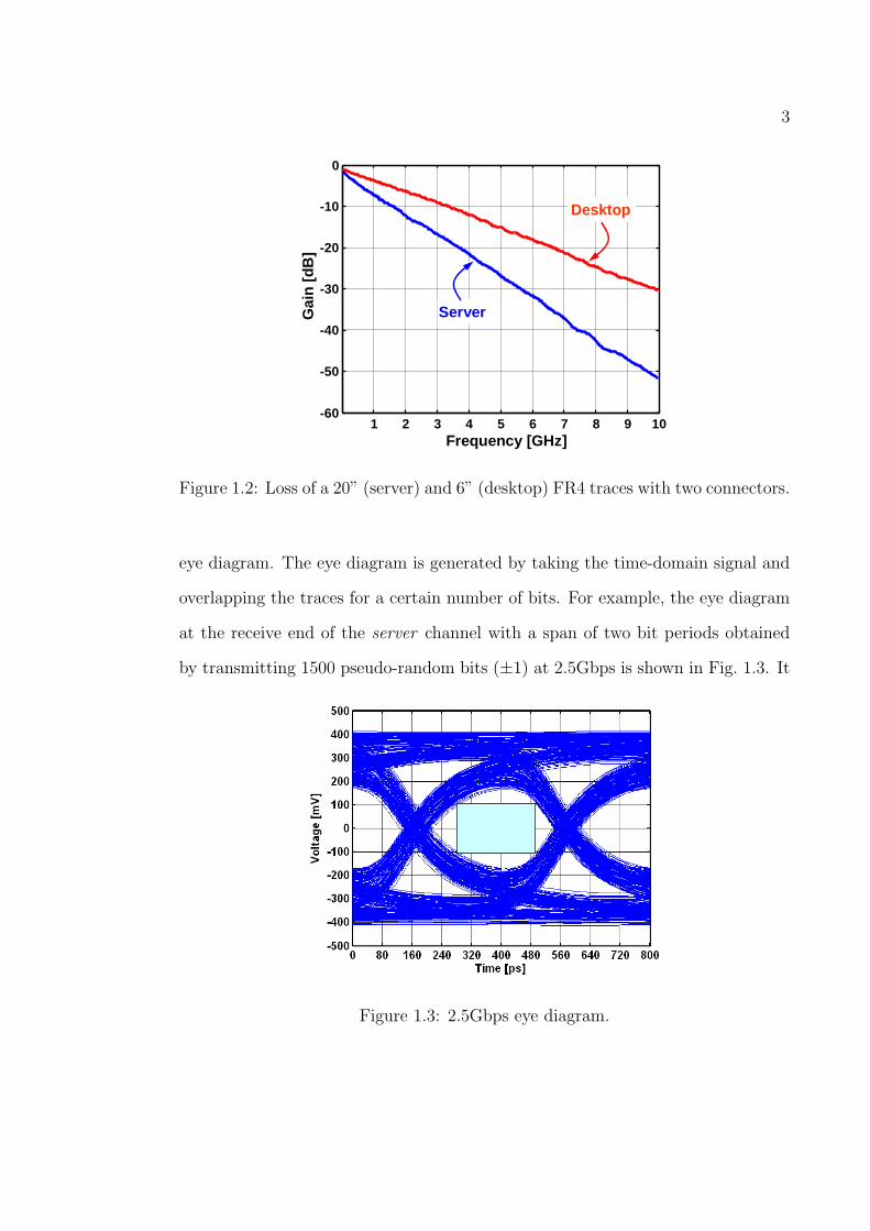
3
1 2 3 4 5 6 7 8 9 10-60
-50
-40
-30
-20
-10
0
Frequency [GHz]
Gai
n [
dB
]
Desktop
Server
Figure 1.2: Loss of a 20” (server) and 6” (desktop) FR4 traces with two connectors.
eye diagram. The eye diagram is generated by taking the time-domain signal and
overlapping the traces for a certain number of bits. For example, the eye diagram
at the receive end of the server channel with a span of two bit periods obtained
by transmitting 1500 pseudo-random bits (±1) at 2.5Gbps is shown in Fig. 1.3. It
Figure 1.3: 2.5Gbps eye diagram.
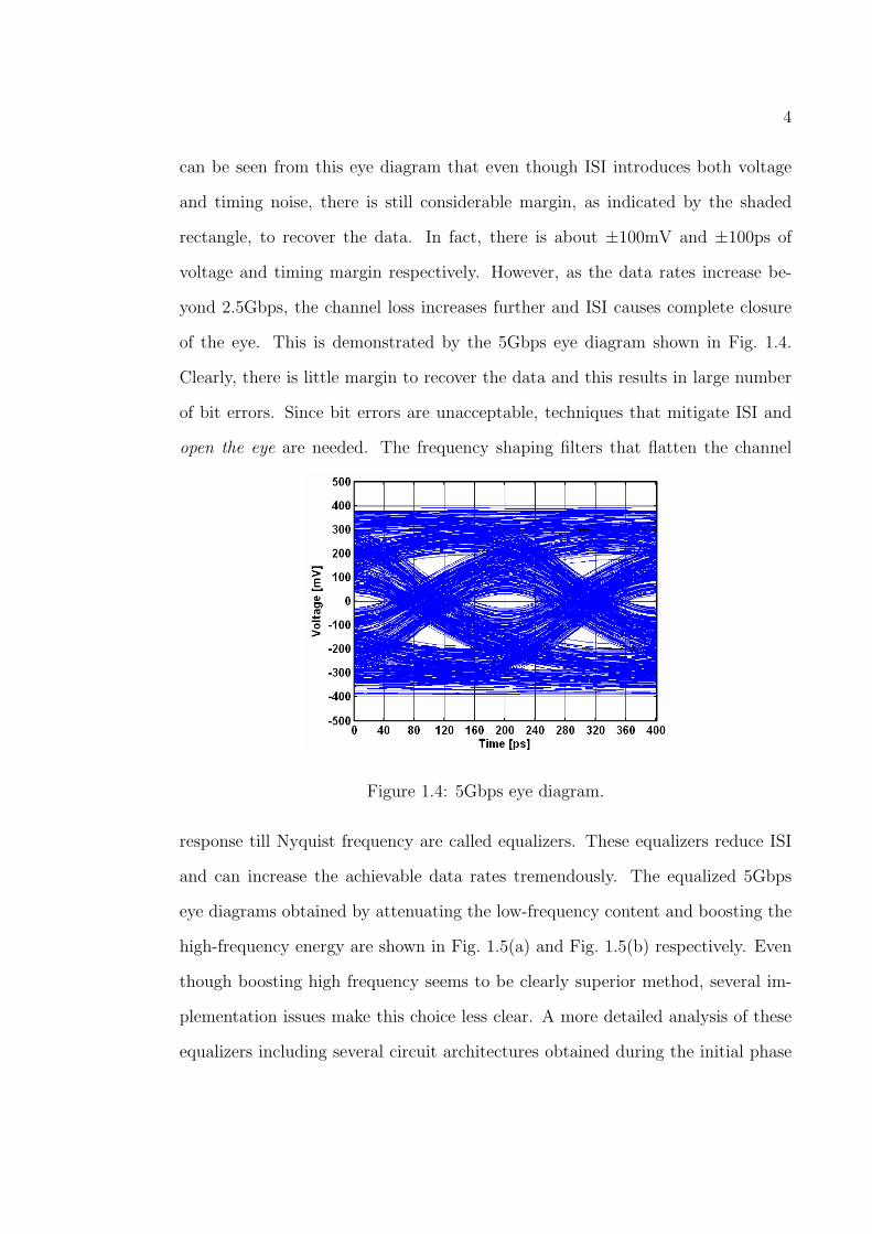
4
can be seen from this eye diagram that even though ISI introduces both voltage
and timing noise, there is still considerable margin, as indicated by the shaded
rectangle, to recover the data. In fact, there is about ±100mV and ±100ps of
voltage and timing margin respectively. However, as the data rates increase be-
yond 2.5Gbps, the channel loss increases further and ISI causes complete closure
of the eye. This is demonstrated by the 5Gbps eye diagram shown in Fig. 1.4.
Clearly, there is little margin to recover the data and this results in large number
of bit errors. Since bit errors are unacceptable, techniques that mitigate ISI and
open the eye are needed. The frequency shaping filters that flatten the channel
Figure 1.4: 5Gbps eye diagram.
response till Nyquist frequency are called equalizers. These equalizers reduce ISI
and can increase the achievable data rates tremendously. The equalized 5Gbps
eye diagrams obtained by attenuating the low-frequency content and boosting the
high-frequency energy are shown in Fig. 1.5(a) and Fig. 1.5(b) respectively. Even
though boosting high frequency seems to be clearly superior method, several im-
plementation issues make this choice less clear. A more detailed analysis of these
equalizers including several circuit architectures obtained during the initial phase

5
(a) (b)
Figure 1.5: Equalized 5Gbps eye diagrams: (a) Attenuating low-frequency(b) Boost high-frequency.
of this research are presented in [4]. The focus of the rest of this dissertation is
circuits that enable low-jitter clock and data recovery.
1.2 Clock Jitter
Clock jitter – defined as the uncertainty in the zero-crossings – distorts both
the transmitted data and recovered data and severely affects the bit error rate
(BER) of the link. Reducing the BER is the primary motivation to design low-
jitter clocks. The effect of clock jitter in serial links in depicted in Fig. 2.4. The
Tx side
Rx side
RCK
01 1100
Figure 1.6: Effect of clock jitter in serial links
jitter of the phase locked loop (PLL) directly modulates the transmitted data and

6
the jitter on the recovered clock (RCK) results in sub-optimal sampling of the
incoming data, both of which result in degraded BER. In order to provide a better
view of the effect of jitter, a simulated 5Gbps eye diagram with transmitter clock
jitter is shown in Fig. 1.7. Comparing this to the eye diagram generated with jitter
free PLL in Fig. 1.5(b), the degradation in both the timing and voltage margin is
self evident. In view of these detrimental effects of clock jitter, the focus of this
Figure 1.7: Receive equalized 5Gbps eye diagram with transmitter PLL jitter.
research is to both develop analytical models that enable quick margin analysis in
the presence of clock jitter and to investigate and invent new circuit architectures
that enable low-jitter clock recovery.
1.3 Thesis Organization
Since the focus of this dissertation is techniques to realize low-jitter clocking
schemes, Chapter 2 presents an analysis of the effect of clock jitter in high-speed
links. This analysis provides expressions to estimate voltage and timing margin
7
degradation due to ISI, transmitter and receiver clock jitter.
Chapter 3 discusses the design of digital to phase converters which are the
most important building blocks of source synchronous interfaces. After a brief
review of the drawbacks of the existing solutions, a new architecture that achieves
sub-picosecond resolution is presented.
A mixed analog/digital clock and data recovery architecture that achieves
very high phase and frequency resolution is presented in Chapter 4. This archi-
tecture also provides very wide tracking range making it suitable for systems with
spread-spectrum clocking.
Chapter 5 discusses a digital clock and data recovery circuit, in which analog
blocks such as charge-pump and loop filter are replaced with digital counterparts.
Despite it simplicity, this circuit achieves performance comparable to an analog
clock and data recovery circuit.
CHAPTER 2. PERFORMANCE ANALYSIS METHODS
FOR SERIAL LINKS
As increasing data rates follow technology scaling, limited timing accuracy
that is bound by the unavoidable use of phase- and/or delay-locked loops (PLLs/DLLs)
can significantly degrade link performance. Furthermore, due to the need for inte-
gration of clock generators such as phase-locked loops (PLLs) in large digital chips,
clock jitter is dominated by power supply and substrate noise, both of which do not
scale with technology. As data rates increase, bit periods become shorter and the
performance of most multi-gigabit links will be limited by clock jitter. Therefore,
it is important to analyze the effects of clock jitter on these high speed serial links.
In view of these issues, we need an approach to thoroughly analyze the impact of
PLL clock jitter on serial links to identify and understand weaknesses, to verify
robustness, and to shed light on new techniques to overcome these problems. In
the design phase, transceiver systems typically rely on time-domain simulations
involving a long sequence of random data and the performance of serial links is
often evaluated using eye diagrams of the received data.
There are two problems with this traditional design approach. First, simu-
lation time becomes prohibitively long to evaluate a near worst-case eye diagram.
For example, for a serial link with an expected bit error rate (BER) of 10−12, the
input random sequence should be at least 1012 bits long, and preferably, many
times longer in order to get an accurate statistical measure. Second, it is diffi-
cult to properly simulate these serial links with time-domain jitter contributions
coming from clock sources at both ends (receiver and transmitter) of the link. In

9
practice, several simplifying assumptions are made regarding the effect of clock
jitter on the receive eye diagram. Using these assumptions, the eye diagram gen-
erated without clock jitter is modified to obtain an eye diagram with clock jitter.
One common way to do this is by closing either side of the eye horizontally by the
amount of peak clock jitter. While this method can be helpful in evaluating the
effects of jitter at the receiver end, we will show in the following sections that this
is an overly optimistic approximation of noise margin degradation for transmitter
jitter. In the following sections, an analytical method to incorporate time-domain
clock jitter into the design of high speed serial links is presented. This analysis is
based on the assumption that jitter is small compared to the clock period. This
assumption is valid for well-designed PLLs.
2.1 Worst Case ISI Analysis
Non-return-to-zero (NRZ) pulses are commonly used as basis functions for
discrete data transmission. The response of the channel to the NRZ pulse is defined
as the pulse response and is traditionally used to analyze and model the effects of
a channel on data transmission and also in the design of equalizers in the case of
channels with large attenuation at the frequency of interest. The pulse response is
obtained simply by convolving the channel impulse response with the transmitted
pulse. A conceptual pulse response along with ISI terms are shown in Fig. 2.1.
Since the pulse response is completely deterministic, we can find the sequence of
bits that maximizes the ISI. In other words, we can determine the worst case eye
closure for a given channel response and data rate. Based on the observation that
the total ISI is maximized when negative ISI terms (ISI−) are multiplied with +1
and the positive ISI terms (ISI−) with −1, the worst-case ISI distortion (positive
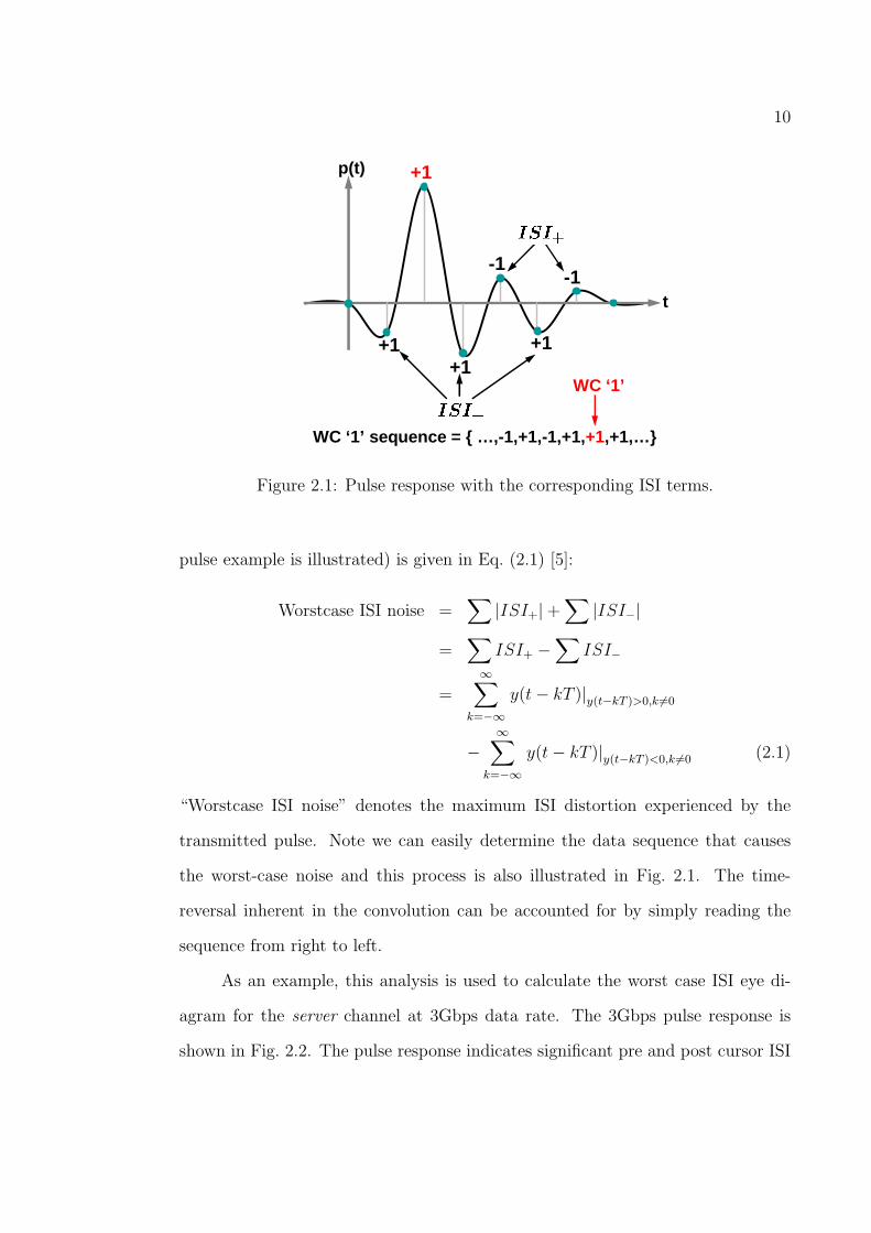
10
t
p(t)
-1-1
+1+1
+1
+1
WC ‘1’
WC ‘1’ sequence = …,-1,+1,-1,+1, +1,+1,…
Figure 2.1: Pulse response with the corresponding ISI terms.
pulse example is illustrated) is given in Eq. (2.1) [5]:
Worstcase ISI noise =∑
|ISI+|+∑
|ISI−|
=∑
ISI+ −∑
ISI−
=∞∑
k=−∞y(t− kT )|y(t−kT )>0,k 6=0
−∞∑
k=−∞y(t− kT )|y(t−kT )<0,k 6=0 (2.1)
“Worstcase ISI noise” denotes the maximum ISI distortion experienced by the
transmitted pulse. Note we can easily determine the data sequence that causes
the worst-case noise and this process is also illustrated in Fig. 2.1. The time-
reversal inherent in the convolution can be accounted for by simply reading the
sequence from right to left.
As an example, this analysis is used to calculate the worst case ISI eye di-
agram for the server channel at 3Gbps data rate. The 3Gbps pulse response is
shown in Fig. 2.2. The pulse response indicates significant pre and post cursor ISI

11
0 1 2 3 4 5 6 7 8-0.1
0
0.1
0.2
0.3
0.4
0.5
0.6
0.7
Vo
ltag
e [V
]
Time [ns]
Figure 2.2: 3Gbps pulse response.
terms. These ISI terms reduce the voltage margin at the receiver as illustrated by
the receive eye diagram in Fig. 2.3. This eye diagram is the result of long tran-
sient simulations in which about 2000 random data bits are transmitted across
the channel. Also shown in the figure is the worst case (WC) eye obtained by the
analysis described above. This figure illustrates that the simulated eye diagram
approaches the worst case eye only with very long data streams.
2.2 Analysis of Clock Jitter
Even though the pulse response is very useful for characterizing the ISI, we
will find that it is very difficult to analyze the effects of PLL jitter (especially
transmitter jitter) because a pulse is created by two adjacent edges with jitter.
Consider the serial link model shown in Fig. 2.4. Qualitatively, jitter in the trans-
mit PLL modulates the width of the transmitted NRZ data pulse. This modulation

12
WC eye
Figure 2.3: 3Gbps simulated and worst case eye diagrams.
being random, the pulse response of the system displays a level of random varia-
tion in accordance with the jitter. This makes the usage of standard deterministic
methods difficult. In the case of receiver sampling jitter, several approaches to
estimate the signal-to-noise ratio (SNR) loss due to jitter have been proposed [6].
However, it is difficult to translate SNR loss to a reduction of the noise-margin or
degradation of the bit error rate (BER) in the case of serial links. To circumvent
these problems we need a unifying analysis to accommodate both the transmitter
and receiver sampling jitter to calculate the worst-case noise margin degradations.
The following analysis and discussions are formulated in the context of a two-level
PLL CDR
Figure 2.4: Serial link model with transmitter and receiver clock jitter.

13
(single-bit-per-symbol) NRZ transceiver system, as this is the most common mod-
ulation scheme used in serial links today. Some recent implementations employ
four-level NRZ signaling (i.e., PAM-4) which doubles the bits-per-symbol rate.
While our analysis and conclusions can easily be transferred to this and a variety
of other signaling systems, we stay with the common two-level (binary) NRZ sig-
naling scheme to focus our investigations on how PLL jitter impacts transceiver
performance.
2.3 Receiver Clock Jitter
The block diagram used to analyze the clock jitter in the receiver is shown
in Fig. 2.5. The sequence of bits (symbols) communicated to the receiver by the
transmitter can be considered equally likely and independent of each other. We
denote these bits by an independent and identically distributed (i.i.d.) sequence
dk. The transmitter produces an output pulse corresponding to data bit dk
and the variation in the pulse width is determined by the transmitter clock jitter
generated by a PLL. We begin our analysis by focusing on the effects of jitter on the
CDR
Figure 2.5: Receiver with recovered clock jitter.
receiver end and assume that the transmitter clock is jitter free. Later sections will
consider the effects of jitter only at the transmitter and the combination of jitter
14
on both transmit and receive clocks. This means that the pulses corresponding to
all data bits have equal width. With this assumption, the transmitted pulse train
φ(t), in terms of the data bit sequence dk, can be written as [7]
φ(t) =∞∑
k=−∞(d[kT ]− d[kT − T ]) · u(t− kT ) , (2.2)
where T is equal to the bit period and u(t) is the unit step function such that
u(t) = 0 for t ≤ 0 and u(t) = 1 for t > 0. The output of the channel, y(t), can be
evaluated by convolving the input pulse train with the channel impulse response
h(t)
y(t) =
[ ∞∑
k=−∞(d[kT ]− d[kT − T ]) · u(t− kT )
]⊗ h(t)
=∞∑
k=−∞[(d[kT ]− d[kT − T ]) · s(t− kT )] , (2.3)
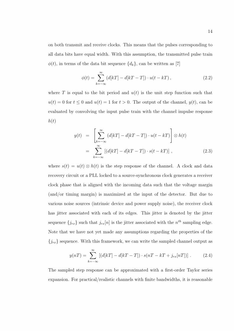
where s(t) = u(t) ⊗ h(t) is the step response of the channel. A clock and data
recovery circuit or a PLL locked to a source-synchronous clock generates a receiver
clock phase that is aligned with the incoming data such that the voltage margin
(and/or timing margin) is maximized at the input of the detector. But due to
various noise sources (intrinsic device and power supply noise), the receiver clock
has jitter associated with each of its edges. This jitter is denoted by the jitter
sequence jrx such that jrx[n] is the jitter associated with the nth sampling edge.
Note that we have not yet made any assumptions regarding the properties of the
jrx sequence. With this framework, we can write the sampled channel output as
y(nT ) =∞∑
k=−∞[(d[kT ]− d[kT − T ]) · s(nT − kT + jrx[nT ])] . (2.4)
The sampled step response can be approximated with a first-order Taylor series
expansion. For practical/realistic channels with finite bandwidths, it is reasonable
15
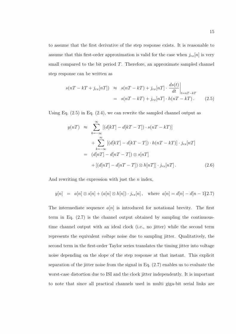
to assume that the first derivative of the step response exists. It is reasonable to
assume that this first-order approximation is valid for the case when jrx[n] is very
small compared to the bit period T . Therefore, an approximate sampled channel
step response can be written as
s(nT − kT + jrx[nT ]) ≈ s(nT − kT ) + jrx[nT ] · ds(t)
dt
∣∣∣∣t=nT−kT
= s(nT − kT ) + jrx[nT ] · h(nT − kT ) . (2.5)
Using Eq. (2.5) in Eq. (2.4), we can rewrite the sampled channel output as
y(nT ) ≈∞∑
k=−∞[(d[kT ]− d[kT − T ]) · s(nT − kT )]
+∞∑
k=−∞[(d[kT ]− d[kT − T ]) · h(nT − kT )] · jrx[nT ]
= (d[nT ]− d[nT − T ])⊗ s[nT ]
+ [(d[nT ]− d[nT − T ])⊗ h[nT ]] · jrx[nT ] . (2.6)
And rewriting the expression with just the n index,
y[n] = a[n]⊗ s[n] + (a[n]⊗ h[n]) · jrx[n] , where a[n] = d[n]− d[n− 1] .(2.7)
The intermediate sequence a[n] is introduced for notational brevity. The first
term in Eq. (2.7) is the channel output obtained by sampling the continuous-
time channel output with an ideal clock (i.e., no jitter) while the second term
represents the equivalent voltage noise due to sampling jitter. Qualitatively, the
second term in the first-order Taylor series translates the timing jitter into voltage
noise depending on the slope of the step response at that instant. This explicit
separation of the jitter noise from the signal in Eq. (2.7) enables us to evaluate the
worst-case distortion due to ISI and the clock jitter independently. It is important
to note that since all practical channels used in multi giga-bit serial links are
16
significantly bandwidth limited, the step response of the channel rises/falls quite
slowly. This slow rise/fall translates to high accuracy of the first-order Taylor
series. In the case of distortion introduced by clock jitter, the worst-case condition
can be evaluated by observing the effect of jitter due to the worst-case ISI data
pattern as illustrated in Fig. 2.1. The corresponding jitter noise can be evaluated
using the second term of Eq. (2.7), (a[n]⊗ h[n]) · jrx[n], by
Receiver Jitter Noise = (a[n]⊗ h[n]) ·max(jrx[n]) , (2.8)
where a[n] is the worst-case/peak ISI distortion data sequence derived using Eq. (2.1).
0 50 100 150 200 250 300 350-0.2
-0.15
-0.1
-0.05
0
0.05
0.1
0.15
0.2
Time [ps]
Vo
ltag
e [V
]
Simulated3σσσσ Jitter7σσσσ Jitter
Figure 2.6: Eye diagrams with receiver clock jitter.
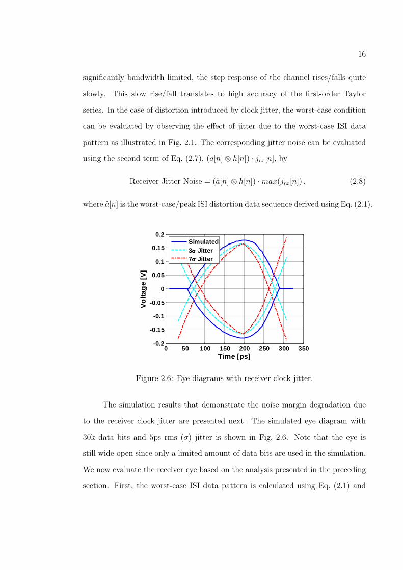
The simulation results that demonstrate the noise margin degradation due
to the receiver clock jitter are presented next. The simulated eye diagram with
30k data bits and 5ps rms (σ) jitter is shown in Fig. 2.6. Note that the eye is
still wide-open since only a limited amount of data bits are used in the simulation.
We now evaluate the receiver eye based on the analysis presented in the preceding
section. First, the worst-case ISI data pattern is calculated using Eq. (2.1) and

17
the jitter noise generated due to this data pattern is calculated using Eq. (2.8).
The worst-case eye is then obtained by subtracting the jitter noise from the worst-
case ISI eye. The calculated worst-case eye diagrams using 3σ and 7σ amounts
of peak jitter are shown in Fig. 2.6. The noise margin degradation is minimal at
the center of the eye and maximum near the zero-crossing. This makes intuitive
sense because the center of the eye is reasonably flat (slope is zero) and hence
any jitter at the optimal sampling point only results in a small voltage margin
degradation. However, due to the larger slope at the edges, jitter translates to a
larger voltage margin degradation at the edge of the eye. Also, notice that even
with 30k data bits, the simulated eye is not close to the calculated worst-case eye
with 3σ jitter. This reinforces the fact that it is generally very difficult to find the
absolute worst-case margin from time-domain simulations. For this reason, time-
domain simulation is seldom used to estimate BER in practice. Commonly used
methods incorporate the effects of jitter into the worst-case ISI eye by shifting the
ISI eye edges horizontally towards the center of the eye by the peak jitter amount.
Even though this method results in a worst-case eye, it provides little insight and
is not applicable to the transmitter jitter.
In the case of severely ISI-limited channels, equalization is used to recover
some of the high frequency content lost through the channel. An equalizer is
typically a filter which inverts the channel response so that the overall response is
essentially flat in the band of interest (up to the Nyquist rate of the data), thus
reducing the effects of ISI. In serial links employing equalizers, the detector input is
simply the sampled channel output convolved with the filter with impulse response
W . This is given by
yeq[n] = a[n]⊗ s[n]⊗W [n] + (a[n]⊗ h[n]) · jrx[n] ⊗W [n] . (2.9)

18
The worst-case jitter noise and ISI data patterns can be calculated in a similar
way as shown earlier in the case without equalization.
2.4 Transmitter Clock Jitter
The block diagram used to analyze the clock jitter in the transmitter is shown
in Fig. 2.7. The transmitter clock determines the pulse width of the transmitted bit
or symbol. With transmitter clock jitter, the pulse width of the transmitted data
bit can be viewed as being modulated by the jitter. This causes degradation of the
noise margin at the detector input for the following reasons. First, the transmitter
clock jitter causes sub-optimal sampling at the receiver due to the limited tracking
bandwidth of the timing-recovery loop. Second, in the case of equalized serial
links, the transmitter jitter degrades the equalizer performance. This is because
the equalizers are normally optimized for a specific pulse response. Even in the case
of adaptive equalizers, the high frequency content of the jitter cannot be tracked
due to typically large time constants of the adaptation algorithms [8]. We will now
PLL
01 1100
Figure 2.7: Transmitter with PLL clock jitter.
show that the transmit jitter can be analyzed in a similar framework as shown for
receiver sampling clock jitter previously in Section 2.3. Consider Eq. (2.3) repeated

19
below for convenience:
y(t) =
[ ∞∑
k=−∞(d[kT ]− d[kT − T ]) · u(t− kT )
]⊗ h(t)
=∞∑
k=−∞[(d[kT ]− d[kT − T ]) · s(t− kT )] .
In this equation, the sampling instant kT determines the pulse width of the kth
transmitted data pulse/bit. The jitter in the transmitter can be included in the
above equation by defining a jitter sequence jtx such that jtx[k] is the jitter
associated with the kth clock edge:
y(t) =
[ ∞∑
k=−∞(d[kT ]− d[kT − T ]) · u(t− kT − jtx[kT ])
]⊗ h(t)
=∞∑
k=−∞[(d[kT ]− d[kT − T ]) · s(t− kT − jtx[kT ])] . (2.10)
Again, a first-order Taylor series expansion can be used if jtx[k] ¿ T , and the
approximate channel output can be written as
y(t) ≈∞∑
k=−∞[(d[kT ]− d[kT − T ]) · s(t− kT )]
+∞∑
k=−∞[(d[kT ]− d[kT − T ]) · h(t− kT ) · jtx[kT ])] . (2.11)
In order to estimate the effects of transmitter clock jitter alone, let us assume
for now that the receiver sampling clock is jitter free. In this case, the sampled
channel output can be written as
y(nT ) =∞∑
k=−∞[(d[kT ]− d[kT − T ]) · s(nT − kT )]
+∞∑
k=−∞[(d[kT ]− d[kT − T ]) · h(nT − kT ) · jtx[kT ])]
=∞∑
k=−∞[a[kT ] · s(nT − kT )]
+∞∑
k=−∞[(a[kT ] · jtx[kT ]) · h(nT − kT )] . (2.12)

20
And rewriting this first-order approximated output expression with just the n
index,
y[n] = a[n]⊗ s[n] + (a[n] · jtx[n])⊗ h[n] . (2.13)
Unlike the receiver sampling jitter of Eq. (2.7), the transmitted data difference
sequence a[n] is first modulated by the transmitter jitter sequence jtx[n] and then
the resulting sequence is convolved with the channel’s impulse response h[n].
Once again, the peak ISI distortion inherent in the first convolution term
in Eq. (2.13) can be calculated using Eq. (2.1). However, the peak distortion
due to the transmitter jitter noise is different from that of the receiver sampling
jitter. Intuitively, we expect the transmit jitter to be filtered by the channel in
some fashion and the second term in Eq. (2.13) reinforces our intuition. Due to
the modulation of a[n] by the jitter sequence jtx[n], we can evaluate the peak
distortion due to the transmitter clock jitter, i.e., the peak distortion of the second
term (a[n] · jtx[n])⊗ h[n], by
Transmit Jitter Noise = (|a[n]| ·max(jtx[n]))⊗ |h[n]| , (2.14)
where a[n] is the worst-case/peak ISI distortion data sequence derived using Eq. (2.1).
It is interesting to note that the peak distortion due to the transmitter clock jitter
noise can be potentially greater than that of the receiver sampling jitter for the
similar amounts of receiver (jrx) and transmitter (jtx) jitter.
Similar to the receiver sampling jitter case, the simulated and calculated
worst-case eye diagrams with the transmitter jitter are shown in Fig. 2.8. Again,
the simulated eye is not close to the calculated worst-case eye even with 3σ jitter.
It is interesting to note that the noise margin degradation due to transmitter
jitter is severe all across the eye unlike the receiver jitter case, where degradation
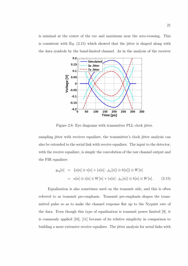
21
is minimal at the center of the eye and maximum near the zero-crossing. This
is consistent with Eq. (2.15) which showed that the jitter is shaped along with
the data symbols by the band-limited channel. As in the analysis of the receiver
0 50 100 150 200 250 300 350-0.2
-0.15
-0.1
-0.05
0
0.05
0.1
0.15
0.2
Time [ps]
Vo
ltag
e [V
]
Simulated3σσσσ Jitter7σσσσ Jitter
Figure 2.8: Eye diagrams with transmitter PLL clock jitter.
sampling jitter with receiver equalizer, the transmitter’s clock jitter analysis can
also be extended to the serial link with receive equalizer. The input to the detector,
with the receive equalizer, is simply the convolution of the raw channel output and
the FIR equalizer:
yeq[n] = a[n]⊗ s[n] + (a[n] · jtx[n])⊗ h[n] ⊗W [n]
= a[n]⊗ s[n]⊗W [n] + (a[n] · jtx[n])⊗ h[n]⊗W [n] . (2.15)
Equalization is also sometimes used on the transmit side, and this is often
referred to as transmit pre-emphasis. Transmit pre-emphasis shapes the trans-
mitted pulse so as to make the channel response flat up to the Nyquist rate of
the data. Even though this type of equalization is transmit power limited [9], it
is commonly applied [10], [11] because of its relative simplicity in comparison to
building a more extensive receive equalizer. The jitter analysis for serial links with

22
transmit equalizer/pre-emphasis directly follows from Eqs. (2.7) and (2.13) with
a corresponding equalized/pre-emphasized data sequence dk.
2.5 Transmitter Jitter and Receiver Jitter
We analyzed transmitter jitter and receiver sampling jitter independently
until now. This was done to demonstrate the effect of each of the jitter terms
independently. Because both effects of jitter typically appear together in a serial
link, we now summarize how the above analysis can be extended to include both
the transmitter and receiver jitter. Equation (2.10) defines the channel output
with transmitter jitter and Eq. (2.4) was derived to consider receive sampling
jitter. Combining the results of Eqs. (2.10) and (2.4), we can re-write the sampled
channel output which incorporates both of the jitter terms:
y(nT ) =∞∑
k=−∞[(d[kT ]− d[kT − T ]) · s(nT − kT + jrx[nT ]− jtx[kT ])] . (2.16)
Once again, we can approximate the step response using a first-order Taylor series
approximation for two variables (i.e. when jtx[k] ¿ T and jrx[k] ¿ T ):
s(nT − kT + jrx[nT ]− jtx[kT ]) ≈ s(nT − kT )
+jrx[nT ] · ds(t)
dt
∣∣∣∣t=nT−kT
− jtx[kT ] · ds(t)
dt
∣∣∣∣t=nT−kT
= s(nT − kT )
+jrx[nT ] · h(nT − kT )
+jtx[kT ] · h(nT − kT ) . (2.17)
Putting Eqs. (2.16) and (2.17) together, we can write the channel output as
y[n] ≈ a[n]⊗ s[n] + (a[n]⊗ h[n]) · jrx[n] + (a[n] · jtx[n])⊗ h[n] . (2.18)

23
Since we did not use any specific properties of the jitter sequence, Eq. (2.18) is
valid for any jitter sequences jtx[n] and jrx[n]. The correlation between jtx[n] and
jrx[n], if any, is determined by the clocking scheme and the system. By defining the
jitter sequences accordingly, the trade-offs between various clocking schemes (e.g.
mesochronous, source synchronous, and embedded clocking [3]) can be analyzed
using Eq. (2.18).
The properties of the individual jitter sequence depend on the type of clock
source used and the system architecture of the serial link. In most situations, it
would be reasonable to assume for the worst case that the transmitter and the re-
ceiver jitter properties are uncorrelated. However, any amount of observed correla-
tion between the transmit and receive jitter would result in an overall improvement
of the system. The calculated eye-diagram incorporating both the transmitter and
receiver jitter is shown in Fig. 2.9. Eye diagrams calculated using zero jitter (i.e.,
only worst-case ISI), transmitter jitter alone, and receiver jitter alone are also
shown. It is clear that the transmitter and receiver jitter degrade both the voltage
margin and the timing margin. However, the transmitter jitter has a more adverse
affect on both the voltage and timing margins.
2.6 Summary
The analysis and net effects of receiver and transmitter clock jitter on high-
speed serial links are presented in this chapter. In particular, the effect of trans-
mitter clock jitter and receiver sampling jitter on the worst-case ISI condition is
analyzed. Based on the linear time-invariant assumptions of the channel and using
the first-order Taylor series approximation, analytical expressions representing the
detector input for various conditions are derived. Interestingly, this analysis shows

24
0 50 100 150 200 250 300 350-0.2
-0.15
-0.1
-0.05
0
0.05
0.1
0.15
0.2
Time [ps]
Vo
ltag
e [V
]
No JitterRx JitterTx JitterTx and Rx Jitter
Figure 2.9: Eye diagrams with transmitter PLL clock and recovered clock jitter.
that the transmitter jitter has more deleterious effect on the link performance
compared to receiver jitter. The noise due to jitter was decoupled from the expres-
sion of the channel output without jitter. This enables efficient calculation of the
noise margin degradation due to jitter. Mathematical expressions useful for cal-
culating the receive and transmit jitter degradations are summarized. Behavioral
simulations indicate a good match between the calculation and simulation. This
analysis enables efficient calculation of the worst-case margin without indulging in
prohibitively long simulations.

CHAPTER 3. HIGH RESOLUTION
DIGITAL-TO-PHASE CONVERTERS
Source-synchronous interfaces are a class of point-to-point links that are
widely used in microprocessors and communication switches. A simplified block
diagram of a typical source-synchronous interface is shown in Fig. 3.1. In this
PLL
DPC1
D Q
DIN1
D Q
DPC2
DIN2
DATA CHANNEL1
DATA CHANNEL2
CLOCK CHANNEL
T + ∆∆∆∆T1
T
T + ∆∆∆∆T2
Figure 3.1: A typical source-synchronous interface.
system, a clock is transmitted along with the data on a separate channel to the
receiver. In order to reduce the overhead of an extra channel, the clock channel is
shared among multiple data channels. The clock edges are synchronized with the
data transitions at the transmitter. If the data and clock transmission lines are
perfectly matched, the time of flight of the data and the clock are equal and as
a result, clock and data remain synchronized at the receiver as well. However, as
data rates increase to multi-gigabit range, it is uneconomical to match the time of

26
flight of clock and data to pico-second accuracy. This mismatch results in a skew
between the clock and data at the receiver causing sub-optimal sampling of the
incoming data. In order to improve the timing margin by reducing the skew be-
tween the received clock and data, a method to introduce a controlled phase shift
on the clock is needed. The focus of the rest of the chapter is the implementation
of circuits that provide a means to introduce such a programmable phase shift. A
digital to phase converter (DPC) is one such circuit block that is often used to
introduce a phase shift whose amount is controlled by an input digital word DIN.
It is important to note that the resolution of the DPC is of paramount importance
as this determines the residual skew between the clock and data which in turn
directly affects the bit-error-rate (BER) of the link. Even though the design of
the DPC is presented in the context of source-synchronous interfaces, it is worth
mentioning that there are several other applications for digital to phase converters
in measurement instrumentation and the techniques developed here can be directly
applied in those applications.
Before we present the proposed DPC architecture it is instructive to review
the disadvantages of existing architectures. One of the earliest implementations of
the DPC is shown in Fig. 3.2 [12]. It consists of a multi phase generator which
Multi Phase Generator
ΦΦΦΦ1 ΦΦΦΦ2
∆∆∆∆TΦΦΦΦN
DIN N:1 MUX
ΦΦΦΦOUT
Figure 3.2: DPC using phase selection.
provides N clock phases separated by a delay of ∆T. These multiple phases (Φ1 to

27
ΦN) are typically generated through a chain of inverters whose delay is precisely
adjusted to ∆T by a feedback loop. An N-to-1 mux is used to select one of the
N phases based on the input digital word DIN, thereby introducing a phase shift
in steps of ∆T on the output. There are several drawbacks with this approach.
First, the resolution ∆T is limited by the minimum delay of the inverter in a
given process. Second, since ∆T is equal to a fraction of the clock period (Tperiod
N)
the resolution scales directly with the frequency, thereby degrading it at a lower
operating frequency. Finally, the phase selection process introduces unwanted
discrete phase jumps in the output phase. Despite its simplicity, due to these
performance limiting factors, the use of this DPC is very limited in multi-giga bit
interfaces.
A more commonly used DPC architecture that overcomes some of these draw-
backs is depicted in Fig. 3.3 [13], [14], [15]. This architecture combines the phase
DIN
Multi Phase Generator
ΦΦΦΦ1 ΦΦΦΦ2
∆∆∆∆TΦΦΦΦN
ΦΦΦΦOUT
ΦΦΦΦINTERPOLATOR
MSBs
LSBs
ΦΦΦΦj ΦΦΦΦj+1
N:2 MUX∆∆∆∆T
Figure 3.3: DPC using phase selection and interpolation.
selecting multiplexer with a phase interpolator. The most significant bits (MSBs)
of the input digital word are used to select two adjacent phases, Φj, Φj+1, from the
N phases using an N:2 multiplexer (mux). These two phases are interpolated by
a phase interpolator controlled by the least significant bits (LSBs) to generate the
required output phase ΦOUT. As a result of phase interpolation, the resolution of
28
this DPC is not limited by the minimum inverter delay. However, the effectiveness
of the interpolation depends largely on the input rise time, phase separation ∆T,
and the interpolator output time constant.
∆∆∆∆Tαααα = 0.5
Vj
Vj+1
VOUT
(a)
R
CααααImax(1-αααα)Imax
Vj Vj+1
VOUT
(b)
VDD
Figure 3.4: Phase interpolator: (a) Operation (b) Model.
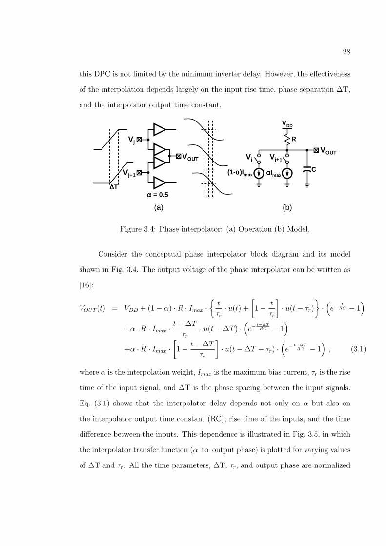
Consider the conceptual phase interpolator block diagram and its model
shown in Fig. 3.4. The output voltage of the phase interpolator can be written as
[16]:
VOUT (t) = VDD + (1− α) ·R · Imax ·
t
τr
· u(t) +
[1− t
τr
]· u(t− τr)
·(e−
tRC − 1
)
+α ·R · Imax · t−∆T
τr
· u(t−∆T ) ·(e−
t−∆TRC − 1
)
+α ·R · Imax ·[1− t−∆T
τr
]· u(t−∆T − τr) ·
(e−
t−∆TRC − 1
), (3.1)
where α is the interpolation weight, Imax is the maximum bias current, τr is the rise
time of the input signal, and ∆T is the phase spacing between the input signals.
Eq. (3.1) shows that the interpolator delay depends not only on α but also on
the interpolator output time constant (RC), rise time of the inputs, and the time
difference between the inputs. This dependence is illustrated in Fig. 3.5, in which
the interpolator transfer function (α–to–output phase) is plotted for varying values
of ∆T and τr. All the time parameters, ∆T, τr, and output phase are normalized
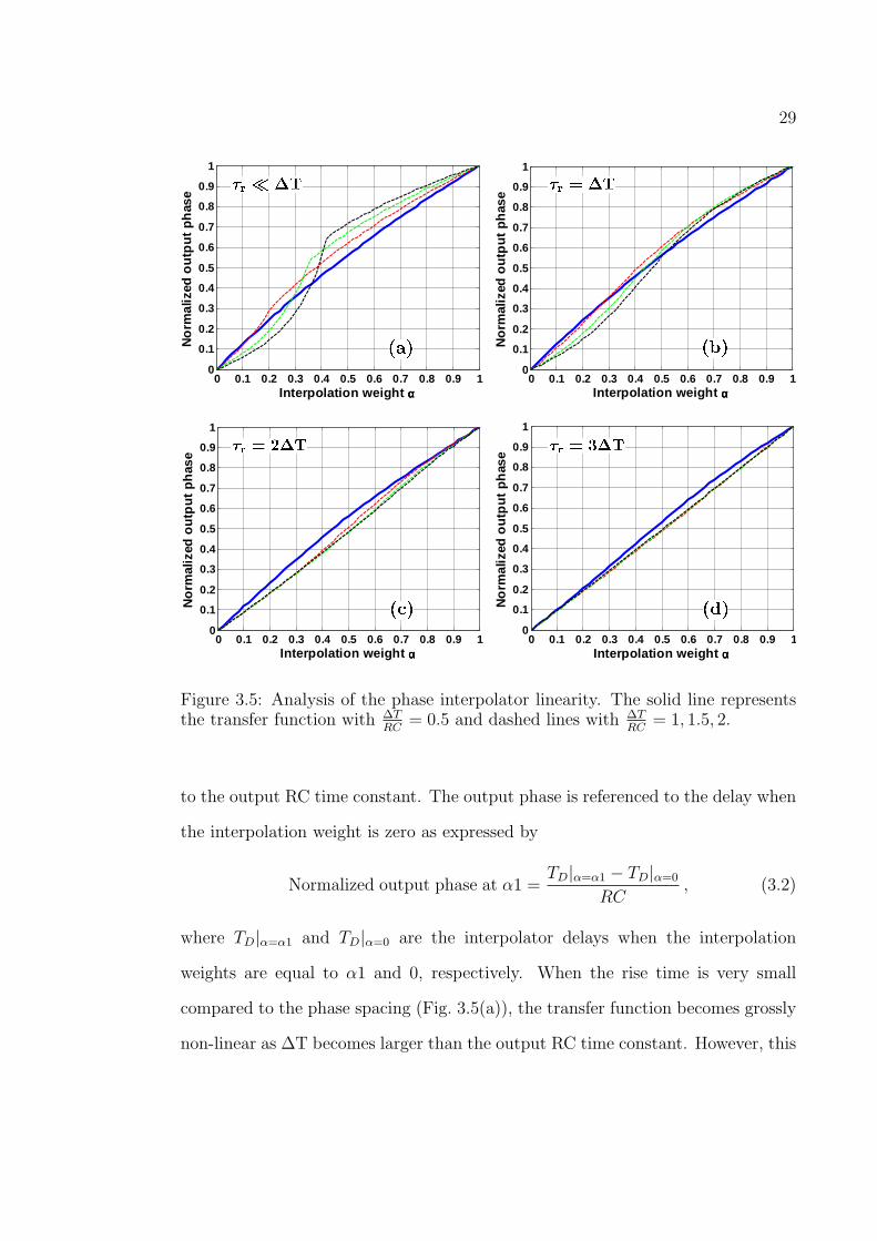
29
0 0.1 0.2 0.3 0.4 0.5 0.6 0.7 0.8 0.9 10
0.1
0.2
0.3
0.4
0.5
0.6
0.7
0.8
0.9
1
No
rmal
ized
ou
tpu
t p
has
e
Interpolation weight αααα0 0.1 0.2 0.3 0.4 0.5 0.6 0.7 0.8 0.9 1
0
0.1
0.2
0.3
0.4
0.5
0.6
0.7
0.8
0.9
1
No
rmal
ized
ou
tpu
t p
has
e
Interpolation weight αααα
0 0.1 0.2 0.3 0.4 0.5 0.6 0.7 0.8 0.9 10
0.1
0.2
0.3
0.4
0.5
0.6
0.7
0.8
0.9
1
No
rmal
ized
ou
tpu
t p
has
e
Interpolation weight αααα0 0.1 0.2 0.3 0.4 0.5 0.6 0.7 0.8 0.9 1
0
0.1
0.2
0.3
0.4
0.5
0.6
0.7
0.8
0.9
1
No
rmal
ized
ou
tpu
t p
has
e
Interpolation weight αααα
Figure 3.5: Analysis of the phase interpolator linearity. The solid line representsthe transfer function with ∆T
RC= 0.5 and dashed lines with ∆T
RC= 1, 1.5, 2.
to the output RC time constant. The output phase is referenced to the delay when
the interpolation weight is zero as expressed by
Normalized output phase at α1 =TD|α=α1 − TD|α=0
RC, (3.2)
where TD|α=α1 and TD|α=0 are the interpolator delays when the interpolation
weights are equal to α1 and 0, respectively. When the rise time is very small
compared to the phase spacing (Fig. 3.5(a)), the transfer function becomes grossly
non-linear as ∆T becomes larger than the output RC time constant. However, this

30
significant non-linearity is gradually reduced as the input rise time is increased as
indicated by Figs. 3.5(b), (c) and (d). The slow rise times needed to achieve good
linearity degrade the jitter immunity of the output clock [17]. The resolution of
this architecture also depends on the operating frequency. The non-linearity of the
interpolator increases with increasing phase separation ∆T, thereby degrading the
output phase resolution at a lower operating frequency. Finally, the output jitter of
this architecture is severely affected by the discrete phase jumps introduced during
the input phase switching of the interpolator. A new DPC architecture is proposed
which overcomes these drawbacks and achieves sub pico-second resolution.
3.1 Proposed Architecture
ΦΦΦΦj-1 ΦΦΦΦj+1
N:3 MUXΦΦΦΦj
3:1 MUX
ΦΦΦΦOUT
ΦΦΦΦFILTER
ΦΦΦΦIN
DSM ±1,0
DIN
MSBs
LSBs
Multi Phase Generator
ΦΦΦΦ1 ΦΦΦΦ2∆∆∆∆T ΦΦΦΦN
Figure 3.6: Proposed DPC architecture.
The block diagram of the proposed DPC is shown in Fig. 3.6. Similar to
the earlier implementations, the most significant bits of the input digital word
DIN are used to select the 3 adjacent phases, Φj−1, Φj, and Φj+1 of the N phases
generated by the multi-phase generator. However, as opposed to the previous
implementations, the remaining least significant bits are quantized to 3-levels −1,
31
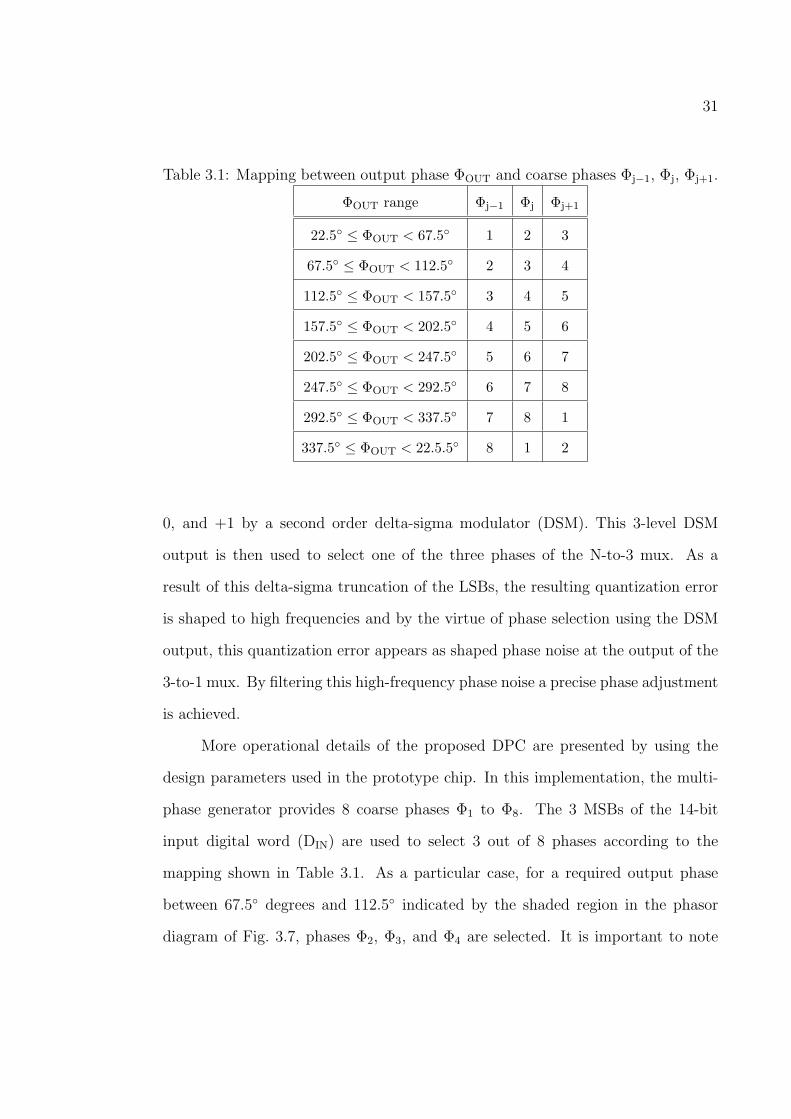
Table 3.1: Mapping between output phase ΦOUT and coarse phases Φj−1, Φj, Φj+1.
ΦOUT range Φj−1 Φj Φj+1
22.5 ≤ ΦOUT < 67.5 1 2 3
67.5 ≤ ΦOUT < 112.5 2 3 4
112.5 ≤ ΦOUT < 157.5 3 4 5
157.5 ≤ ΦOUT < 202.5 4 5 6
202.5 ≤ ΦOUT < 247.5 5 6 7
247.5 ≤ ΦOUT < 292.5 6 7 8
292.5 ≤ ΦOUT < 337.5 7 8 1
337.5 ≤ ΦOUT < 22.5.5 8 1 2
0, and +1 by a second order delta-sigma modulator (DSM). This 3-level DSM
output is then used to select one of the three phases of the N-to-3 mux. As a
result of this delta-sigma truncation of the LSBs, the resulting quantization error
is shaped to high frequencies and by the virtue of phase selection using the DSM
output, this quantization error appears as shaped phase noise at the output of the
3-to-1 mux. By filtering this high-frequency phase noise a precise phase adjustment
is achieved.
More operational details of the proposed DPC are presented by using the
design parameters used in the prototype chip. In this implementation, the multi-
phase generator provides 8 coarse phases Φ1 to Φ8. The 3 MSBs of the 14-bit
input digital word (DIN) are used to select 3 out of 8 phases according to the
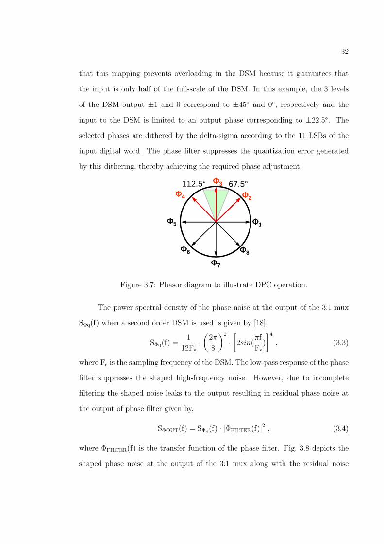
mapping shown in Table 3.1. As a particular case, for a required output phase
between 67.5 degrees and 112.5 indicated by the shaded region in the phasor
diagram of Fig. 3.7, phases Φ2, Φ3, and Φ4 are selected. It is important to note
32
that this mapping prevents overloading in the DSM because it guarantees that
the input is only half of the full-scale of the DSM. In this example, the 3 levels
of the DSM output ±1 and 0 correspond to ±45 and 0, respectively and the
input to the DSM is limited to an output phase corresponding to ±22.5. The
selected phases are dithered by the delta-sigma according to the 11 LSBs of the
input digital word. The phase filter suppresses the quantization error generated
by this dithering, thereby achieving the required phase adjustment.
ΦΦΦΦ1
ΦΦΦΦ2
ΦΦΦΦ3
ΦΦΦΦ5
ΦΦΦΦ6
ΦΦΦΦ7
ΦΦΦΦ8
67.5°112.5°ΦΦΦΦ4
Figure 3.7: Phasor diagram to illustrate DPC operation.
The power spectral density of the phase noise at the output of the 3:1 mux
SΦq(f) when a second order DSM is used is given by [18],
SΦq(f) =1
12Fs
·(
2π
8
)2
·[2sin(
πf
Fs
)
]4
, (3.3)
where Fs is the sampling frequency of the DSM. The low-pass response of the phase
filter suppresses the shaped high-frequency noise. However, due to incomplete
filtering the shaped noise leaks to the output resulting in residual phase noise at
the output of phase filter given by,
SΦOUT(f) = SΦq(f) · |ΦFILTER(f)|2 , (3.4)
where ΦFILTER(f) is the transfer function of the phase filter. Fig. 3.8 depicts the
shaped phase noise at the output of the 3:1 mux along with the residual noise
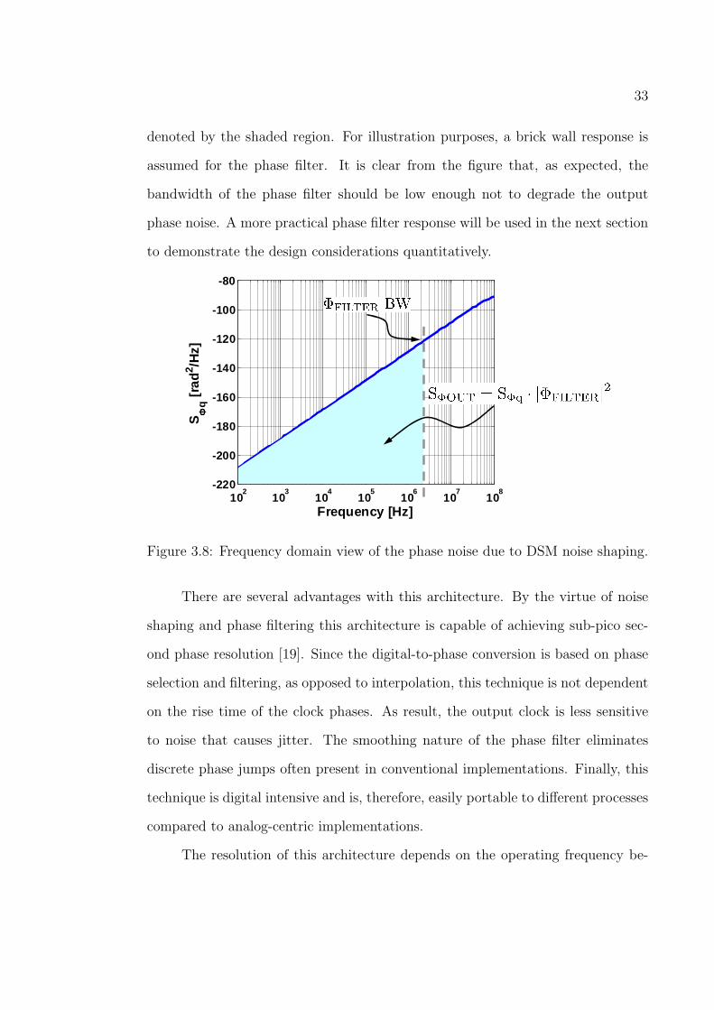
33
denoted by the shaded region. For illustration purposes, a brick wall response is
assumed for the phase filter. It is clear from the figure that, as expected, the
bandwidth of the phase filter should be low enough not to degrade the output
phase noise. A more practical phase filter response will be used in the next section
to demonstrate the design considerations quantitatively.
102
103
104
105
106
107
108
-220
-200
-180
-160
-140
-120
-100
-80
Frequency [Hz]
SΦΦ ΦΦ
q [
rad
2 /Hz]
Figure 3.8: Frequency domain view of the phase noise due to DSM noise shaping.
There are several advantages with this architecture. By the virtue of noise
shaping and phase filtering this architecture is capable of achieving sub-pico sec-
ond phase resolution [19]. Since the digital-to-phase conversion is based on phase
selection and filtering, as opposed to interpolation, this technique is not dependent
on the rise time of the clock phases. As result, the output clock is less sensitive
to noise that causes jitter. The smoothing nature of the phase filter eliminates
discrete phase jumps often present in conventional implementations. Finally, this
technique is digital intensive and is, therefore, easily portable to different processes
compared to analog-centric implementations.
The resolution of this architecture depends on the operating frequency be-

34
cause of the increased phase spacing ∆T at lower operating frequencies. However,
this resolution dependence on operating frequency can be suppressed by designing
a clock jitter limited DPC. If the resolution of the DPC is much higher than the
inherent jitter of the dithered phases, then the reduced resolution will be masked
by the clock jitter. In other words, the phase quantization error of the DPC can be
made lower than the phase noise floor determined by intrinsic noise sources such
as thermal and flicker noise.
3.2 Phase Filter Implementation
One of the most important building blocks of the digital-to-phase converter
is the phase filter. An common choice for a low-pass phase filter is a phase locked
loop. However, as is well known, the design of a high performance PLL poses
several challenges. Notably, jitter accumulation of the VCO results in excessive
output jitter and the suppression of this jitter requires large power dissipation.
The large gain of the VCO in deep sub-micron processes mandates a large loop
filter capacitor that occupies considerable area to stabilize the loop. In addition to
these drawbacks, PLLs also suffer from an inherent noise bandwidth tradeoff. The
input phase noise is suppressed by a low pass transfer function, while the VCO
noise is shaped by a high pass transfer function. In the context of using a PLL as
a phase filter in the DPC, the low bandwidth required to suppress the delta-sigma
noise exacerbates the VCO noise. Because of these disadvantages a PLL phase
filter is not used in the prototype.
Let us now consider the tradeoffs of using a delay-locked loop (DLL) as
a phase filter. The block diagram of a conventional DLL is shown in Fig. 3.9.
Very little jitter accumulation in the voltage controlled delay line (VCDL), results
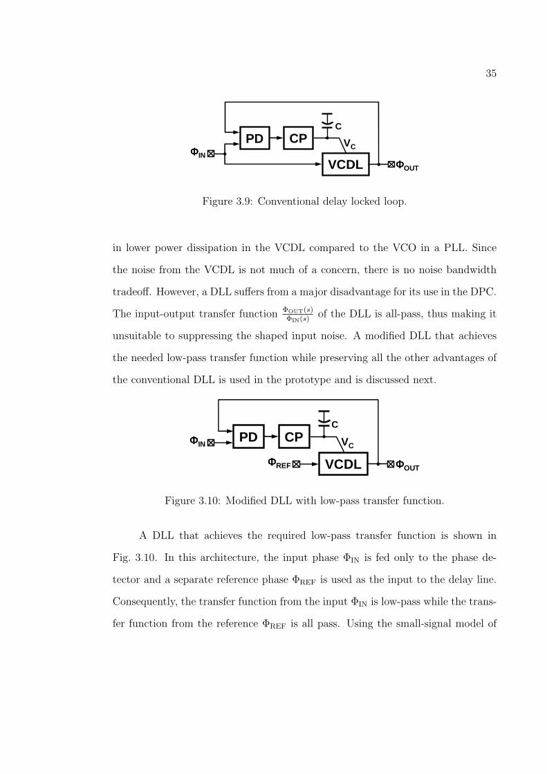
35
PD CP
VCDL
VC
ΦΦΦΦOUT
ΦΦΦΦIN
C
Figure 3.9: Conventional delay locked loop.
in lower power dissipation in the VCDL compared to the VCO in a PLL. Since
the noise from the VCDL is not much of a concern, there is no noise bandwidth
tradeoff. However, a DLL suffers from a major disadvantage for its use in the DPC.
The input-output transfer function ΦOUT(s)ΦIN(s)
of the DLL is all-pass, thus making it
unsuitable to suppressing the shaped input noise. A modified DLL that achieves
the needed low-pass transfer function while preserving all the other advantages of
the conventional DLL is used in the prototype and is discussed next.
PD CP
VCDL
VC
ΦΦΦΦOUT
ΦΦΦΦIN
ΦΦΦΦREF
C
Figure 3.10: Modified DLL with low-pass transfer function.
A DLL that achieves the required low-pass transfer function is shown in
Fig. 3.10. In this architecture, the input phase ΦIN is fed only to the phase de-
tector and a separate reference phase ΦREF is used as the input to the delay line.
Consequently, the transfer function from the input ΦIN is low-pass while the trans-
fer function from the reference ΦREF is all pass. Using the small-signal model of

36
the DLL shown in Fig. 3.11, the input transfer function can be derived as
LG(s) =ICP ·KVCDL · FIN
Cs(3.5)
ΦOUT(s)
ΦIN(s)=
LG(s)
LG(s) + 1(3.6)
=ICP ·KVCDL · Fref
s + ICP ·KVCDL · Fref
, (3.7)
where LG(s) is the loop gain, ICP is the charge pump current, KVCDL is the gain
of VCDL, C is the loop filter capacitance, and FIN is the input frequency.
ΦΦΦΦOUTΦΦΦΦIN
ΦΦΦΦREF
Figure 3.11: Small-signal model of the modified DLL.
There are two important design parameters that determine the achievable
resolution in the proposed architecture. First, the sampling rate of the DSM
determines the effectiveness of noise shaping. For example, in a second order DSM
with a 3-level internal quantizer, the signal-to-quantization ratio improves by 15dB
with a doubling of the sampling frequency [20]. Second, as mentioned earlier, the
bandwidth and the order of the phase filter determine the residual quantization
error. These two parameters, the sampling frequency Fs and the filter bandwidth
BW, are combined to define the effective over sampling rate (OSR) as,
OSR =Fs
2BW. (3.8)
The effectiveness of the first-order DLL phase filter is illustrated by plotting the
residual jitter due to ineffective filtering as shown in Fig. 3.12. This plot is obtained
from behavioral simulations of the DPC using a DLL phase filter whose transfer

37
20 40 60 80 100 120 140 1601
2
3
4
5
6
7
8
OSR
Res
idu
al J
itte
r [m
UI]
Figure 3.12: Residual jitter vs. over sampling ratio for a first-order DLL.
function is given by Eq. (3.7). The x-axis denotes the over-sampling ratio OSR,
and the y-axis shows the residual jitter due to the quantization error leakage that
resulted from incomplete filtering of the shaped noise. This plot indicates that
there is considerable residual jitter even at an OSR of 150. A high OSR translates
to a larger sampling frequency, resulting in larger power dissipation in the DSM.
This excessive residual jitter at lower OSR is mainly due to the fact that the delta
sigma modulator is second order while the DLL is first order.
Before we see how to generate the reference phase, let us consider the two
important design concerns of the DLL when it is used as a phase filter. First, the
non-linearity of the charge pump resulting from current mismatch degrades the
noise performance of the DPC due to noise folding [21]. This mismatch is further
exacerbated by a varying control voltage, VC, needed to achieve the required output
phase based on the input digital word. Second, the quantization error leakage
resulting from inefficient filtering by the DLL reduces the resolution of the DPC.
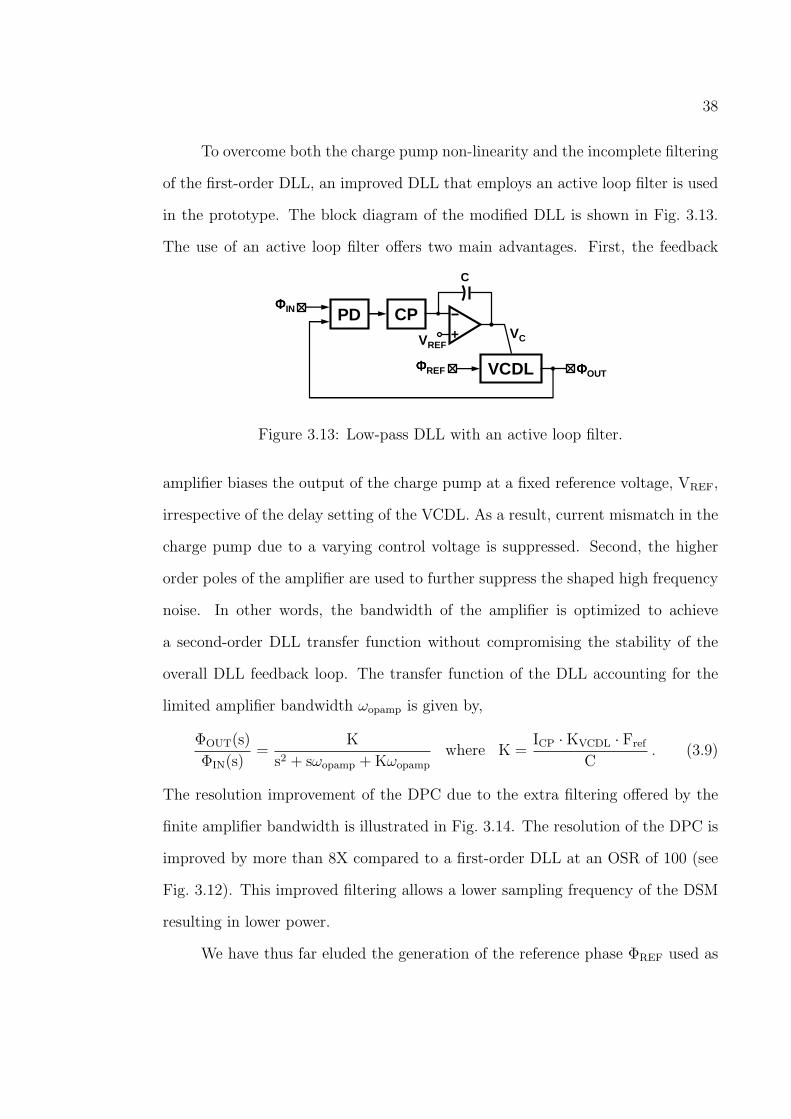
38
To overcome both the charge pump non-linearity and the incomplete filtering
of the first-order DLL, an improved DLL that employs an active loop filter is used
in the prototype. The block diagram of the modified DLL is shown in Fig. 3.13.
The use of an active loop filter offers two main advantages. First, the feedback
ΦΦΦΦIN PD CPVC
VCDL ΦΦΦΦOUTΦΦΦΦREF
+
VREF
C
Figure 3.13: Low-pass DLL with an active loop filter.
amplifier biases the output of the charge pump at a fixed reference voltage, VREF,
irrespective of the delay setting of the VCDL. As a result, current mismatch in the
charge pump due to a varying control voltage is suppressed. Second, the higher
order poles of the amplifier are used to further suppress the shaped high frequency
noise. In other words, the bandwidth of the amplifier is optimized to achieve
a second-order DLL transfer function without compromising the stability of the
overall DLL feedback loop. The transfer function of the DLL accounting for the
limited amplifier bandwidth ωopamp is given by,
ΦOUT(s)
ΦIN(s)=
K
s2 + sωopamp + Kωopamp
where K =ICP ·KVCDL · Fref
C. (3.9)
The resolution improvement of the DPC due to the extra filtering offered by the
finite amplifier bandwidth is illustrated in Fig. 3.14. The resolution of the DPC is
improved by more than 8X compared to a first-order DLL at an OSR of 100 (see
Fig. 3.12). This improved filtering allows a lower sampling frequency of the DSM
resulting in lower power.
We have thus far eluded the generation of the reference phase ΦREF used as

39
20 40 60 80 100 120 140 1600
0.2
0.4
0.6
0.8
1
1.2
1.4
OSR
Res
idu
al J
itte
r [m
UI]
Figure 3.14: Residual jitter vs. over sampling ratio for a second-order DLL.
the input to the VCDL in Fig. 3.13. In the DPC test chip, the reference input to
the DLL is tapped off from one of the 8 phases of the PLL as shown in Fig. 3.15.
As discussed in a later section, false locking in the DLL is avoided by maintaining
an appropriate phase relation between ΦIN and ΦREF at start-up.
Phase Locked Loop
8:3 MUX
3:1 MUX
ΦΦΦΦOUT
ΦΦΦΦIN
±1,0
Delay Locked LoopΦΦΦΦREF
DSM
ΦΦΦΦj-1 ΦΦΦΦj+1ΦΦΦΦjDIN
MSBs
LSBs
Figure 3.15: Complete DPC architecture.

40
3.3 Circuit Design
Phase-Locked Loop Design
The multi-phase generator in Fig. 3.6 is implemented using a phase-locked
loop (PLL) shown in Fig. 4.10. The PLL consists of a phase frequency detector
ΦΦΦΦ1PFD VCOΦΦΦΦ8
REF
÷ 8
CPVC
Figure 3.16: Phase-locked loop that provides 8-phases.
(PFD), a charge pump (CP), a loop filter consisting of a series RC network, a
4-stage voltage controlled ring oscillator (VCO) and a divider in the feedback.
The PFD implemented as a 3-state machine generates a pair of digital pulses
corresponding to the frequency and phase error between the reference clock (REF)
and the fedback divided clock [22]. The CP then converts the digital pulses into
an analog current that is converted to a voltage via the passive loop filter. The
resulting control voltage, VC, drives the VCO. The VCO generates 8 equally spaced
phases Φ1 to Φ8 of which one of the phases is buffered and fed back to the divider.
Dummy inverters are used on the other unused phases to preserve equal spacing
between the adjacent phases. The negative feedback loop forces the frequency and
phase error to zero in steady state.
The schematic of the VCO along with the delay cell is shown in Fig. 5.7. The
delay cell is a simple pseudo-differential inverter in which a PMOS latch is used
to couple the two single-ended current starved inverters to achieve a differential

41
VC
ΦΦΦΦ1 ΦΦΦΦ2 ΦΦΦΦ3 ΦΦΦΦ4ΦΦΦΦ5 ΦΦΦΦ6 ΦΦΦΦ7 ΦΦΦΦ8
VC
Figure 3.17: A 4-stage ring oscillator and the delay cell.
output [23]. The output of the delay cell is buffered to nominally maintain a 50%
duty cycle under process, voltage and temperature variations. Transistor level
simulations indicate that the operating range of the VCO is 0.3GHz – 2GHz and the
gain is 2GHz/V. The simulated VCO phase noise is approximately −110dBc/Hz
at 3MHz offset from the carrier frequency over the whole operating range. Using
the design equations in [24], the charge pump current, loop filter resistor and the
capacitor values are determined to be 15µA, 8KΩ, and 28pF, respectively. These
parameters result in a PLL bandwidth of about 5MHz with a phase margin of 65.
The divider is implemented by a cascade of 3 TSPC divide-by-2 stages [25].
Delay-Locked Loop Design
A brief overview of the delay locked loop with a low-pass transfer function was
presented in Section 3.2. The implementation details of the DLL are presented in
this section. The schematic of the DLL used in the prototype is shown in Fig. 3.18.
It consists of a phase-only detector (PD), a differential charge pump (CP), an active
loop filter and a voltage controlled delay line (VCDL). The phase-only detector
generates digital pulses corresponding the phase difference between the DLL input

42
VREF
PD CPUP
DN UPUPB
DNDNB
VC
VCDL
+
REF OUT
IN
C
DCK
Figure 3.18: Implemented delay-locked loop with active loop filter.
(IN) and delayed clock (DCK). The charge pump converts these digital pulses to
an output current which is filtered by an active integrator. The integrator output
drives the VCDL in a way that forces the phase error to zero. In this locked state,
the delay of the VCDL is typically equal to the period of the input.
Despite the use of phase-only detector, the DLL, if not properly designed,
suffers from start-up problems that can result in a stuck at minimum delay fault
or harmonic locking. Harmonic locking is avoided by resetting the VCDL to its
minimum delay point on start-up [26]. This resetting of the VCDL does not,
however, avoid the DLL from trying to acquire lock to a delay point that is below
the minimum delay offered by the VCDL, resulting in a stuck at minimum delay
fault. This problem arising from two different start-up conditions is illustrated in
Fig. 3.19. In the first case, the minimum delay of the VCDL (TDmin1) is less than
half of the clock period (TPIN). The PD generates a down pulse (DN) indicating
that the delay of the VCDL be further reduced, which results in the DLL getting
stuck to this minimum delay point. Similarly, in the second case, if (TDmin2) is
greater than half of the clock period, the DLL also gets stuck to the minimum
delay point. From these two cases, we can derive the condition on the minimum
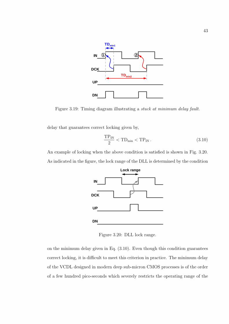
43
IN
DCK
UP
DN
TDmin1
TDmin2
1 2
Figure 3.19: Timing diagram illustrating a stuck at minimum delay fault.
delay that guarantees correct locking given by,
TPIN
2< TDmin < TPIN . (3.10)
An example of locking when the above condition is satisfied is shown in Fig. 3.20.
As indicated in the figure, the lock range of the DLL is determined by the condition
IN
DCK
UP
DN
Lock range
Figure 3.20: DLL lock range.
on the minimum delay given in Eq. (3.10). Even though this condition guarantees
correct locking, it is difficult to meet this criterion in practice. The minimum delay
of the VCDL designed in modern deep sub-micron CMOS processes is of the order
of a few hundred pico-seconds which severely restricts the operating range of the

44
DLL. For example, a four stage VCDL designed in a 0.13µm CMOS process has
a minimum delay of about 200ps, which limits the operating range to 1.25GHz –
2.5GHz. In order to circumvent the limited operating range, the complementary
delay line output is fed back to satisfy the lock range condition in Eq. (3.10). In
other words, a 180 phase shift added to the VCDL output combined with the
small minimum delay guarantees a wide operating range of the implemented DLL.
REF
DCK
DNB
DN
UPB
UP
DN1
UP1
UP1
DN1
DCK
REF
S-to-D
Figure 3.21: Phase-only detector with differential outputs.
The phase-only detector used in the DLL is shown in Fig. 3.21 [27]. This
PD eliminates the extra state in a traditional 3-state phase frequency detector
and as a result prevents loop start-up problems. This PD is designed to produce
narrow output pulses in the steady state to avoid a dead zone. A single-ended-
to-differential (S-to-D) converter is used to generate differential outputs needed
to drive the differential charge pump. The matched delays of the inverter and
the transmission gate along with the cross-coupling through weak inverters in the
S-to-D guarantee fully differential PD outputs.
The four stage voltage controlled delay line along with the delay cell is shown
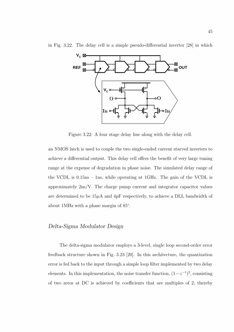
45
in Fig. 3.22. The delay cell is a simple pseudo-differential inverter [28] in which
VC
REF OUT
VC
Figure 3.22: A four stage delay line along with the delay cell.
an NMOS latch is used to couple the two single-ended current starved inverters to
achieve a differential output. This delay cell offers the benefit of very large tuning
range at the expense of degradation in phase noise. The simulated delay range of
the VCDL is 0.15ns – 1ns, while operating at 1GHz. The gain of the VCDL is
approximately 2ns/V. The charge pump current and integrator capacitor values
are determined to be 15µA and 4pF respectively, to achieve a DLL bandwidth of
about 1MHz with a phase margin of 85.
Delta-Sigma Modulator Design
The delta-sigma modulator employs a 3-level, single loop second-order error
feedback structure shown in Fig. 3.23 [20]. In this architecture, the quantization
error is fed back to the input through a simple loop filter implemented by two delay
elements. In this implementation, the noise transfer function, (1−z−1)2, consisting
of two zeros at DC is achieved by coefficients that are multiples of 2, thereby
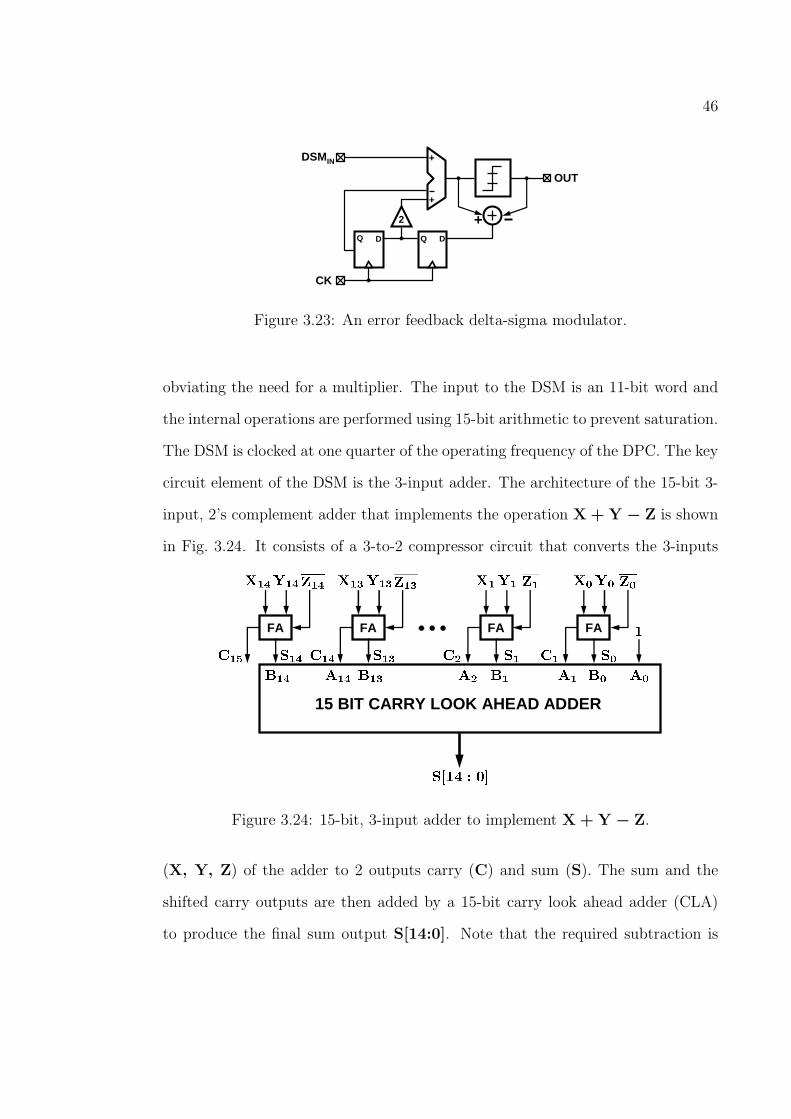
46
DQDQ
2
DSMIN
CK
OUT
+
+
+
Figure 3.23: An error feedback delta-sigma modulator.
obviating the need for a multiplier. The input to the DSM is an 11-bit word and
the internal operations are performed using 15-bit arithmetic to prevent saturation.
The DSM is clocked at one quarter of the operating frequency of the DPC. The key
circuit element of the DSM is the 3-input adder. The architecture of the 15-bit 3-
input, 2’s complement adder that implements the operation X + Y − Z is shown
in Fig. 3.24. It consists of a 3-to-2 compressor circuit that converts the 3-inputs
FA FAFA FA
15 BIT CARRY LOOK AHEAD ADDER
Figure 3.24: 15-bit, 3-input adder to implement X + Y − Z.
(X, Y, Z) of the adder to 2 outputs carry (C) and sum (S). The sum and the
shifted carry outputs are then added by a 15-bit carry look ahead adder (CLA)
to produce the final sum output S[14:0]. Note that the required subtraction is
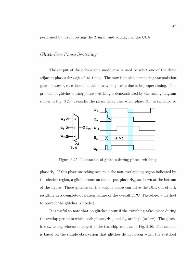
47
performed by first inverting the Z input and adding 1 in the CLA.
Glitch-Free Phase Switching
The output of the delta-sigma modulator is used to select one of the three
adjacent phases through a 3-to-1 mux. The mux is implemented using transmission
gates, however, care should be taken to avoid glitches due to improper timing. This
problem of glitches during phase switching is demonstrated by the timing diagram
shown in Fig. 3.25. Consider the phase delay case when phase Φ−1 is switched to
ΦΦΦΦ+1
ΦΦΦΦ0
ΦΦΦΦ-1
ΦΦΦΦIN
SX -1
0
-1
0
+1ΦΦΦΦ+1
ΦΦΦΦ0
ΦΦΦΦ-1
SX
3
ΦΦΦΦIN
Figure 3.25: Illustration of glitches during phase switching.
phase Φ0. If this phase switching occurs in the non-overlapping region indicated by
the shaded region, a glitch occurs on the output phase ΦIN as shown at the bottom
of the figure. These glitches on the output phase can drive the DLL out-of-lock
resulting in a complete operation failure of the overall DPC. Therefore, a method
to prevent the glitches is needed.
It is useful to note that no glitches occur if the switching takes place during
the overlap period in which both phases, Φ−1 and Φ0, are high (or low). The glitch-
free switching scheme employed in the test chip is shown in Fig. 3.26. This scheme
is based on the simple observation that glitches do not occur when the switched

48
ΦΦΦΦ+1
ΦΦΦΦ0
ΦΦΦΦ-1
CK
SX
S
∆∆∆∆T
TD
2∆∆∆∆T
ΦΦΦΦIN
-1
0
switching instance
Glitch-free zone
D
Q
-1
0
+1
ΦΦΦΦ+1
ΦΦΦΦ0
ΦΦΦΦ-1
SX 3
ΦΦΦΦIN
CK
3S
DFF
Figure 3.26: Glitch-free switching scheme and the associated timing diagram.
phases take on the same value. The control signal Sx is synchronized to the latest
phase Φ+1, so that any phase switching occurs in the shaded region in Fig. 3.26.
This is achieved by synchronizing the mux input control signal S to the phase Φ+1.
Dummy inverters are added on the other two phases, Φ−1, Φ0 to preserve equal
spacing. It is important that the sum of the delays of the inverter and clock-to-Q
delay of the D-flip flop (DFF) be less than 2∆T to ensure a non-zero glitch-free
zone. Mathematically, the following inequality should be satisfied for glitch-free
switching,
TD = TINV + TCK−Q < 2∆T =2TPIN
8. (3.11)
3.4 Experimental Results
The block diagram of the implemented prototype is shown in Fig. 3.27. In
order to obviate the need to measure sub-picosecond time differences, an exclusive

49
±1,0 DIN
2
14
ΦΦΦΦOUT
ΦΦΦΦREF
DPC
REG
VOUT
SDIN
Figure 3.27: Block diagram of the DPC prototype test chip.
OR (XOR) gate is used to convert the phase difference into a voltage. The filtered
XOR output voltage is more easily measured using a high-resolution sampling
oscilloscope. A fully differential XOR gate is implemented by the symmetric archi-
tecture presented in [29] and its simulated transfer function is shown in Fig. 3.28.
The simulated gain of this XOR gate is 2mV/ps. In order to further simplify
-1 -0.75 -0.5 -0.25 0 0.25 0.5 0.75 1-0.5
-0.4
-0.3
-0.2
-0.1
0
0.1
0.2
0.3
0.4
0.5
VP
D [
V]
Phase Error [×××× ππππ radians]
Figure 3.28: Simulated XOR transfer function.
testing, an accumulator is used to generate the 14-bit input digital word from the
serial input SDIN. The complete DPC including the test blocks is fabricated in a

50
0.13µm CMOS process and the chip micrograph is shown in Fig. 3.29. Note that
XOR + LPF
DLL
PLL
MUXDSM
ACCUMULATOR
600µm
800µm
Figure 3.29: DPC chip micrograph.
the DLL occupies a much smaller area than the PLL. The DPC occupies about
0.48mm2 of active die area. The die was packaged in a standard 48-pin LQFP
plastic package. The packaged chip is attached to the 4-layer test board through
a clamp screw that is used to mechanically press the package to force its leads to
contact solder pads on the test board.
The measured transfer function of the DPC operating at 1GHz is presented
in Fig. 3.30. About 6% of the input codes on either end of the transfer curve are
severely affected by the non-linearity of the XOR phase detector and are hence
discarded. The linearity of the DPC is evaluated by plotting the differential and
integral non-linearities shown in Fig. 3.31. The maximum differential non-linearity
(DNL) is less than 0.1ps while the maximum integral non-linearity (INL) is about
12ps. The excellent DNL indicates the effectiveness of the noise shaping of the
delta-sigma modulator and the subsequent filtering of the DLL phase filter. Mea-
sured results also indicate that the DNL and INL are less than ±0.2ps, ±12ps,
respectively over the whole operating range of 0.5GHz – 1.5GHz. This reinforces

51
512 1536 2560 3584 4608 5632 6656 76800
62.5
125
187.5
250
312.5
375
437.5
500
Ou
tpu
t P
has
e [p
s]
Digital Input Code
Figure 3.30: Measured transfer function of the DPC operating at 1GHz.
512 1536 2560 3584 4608 5632 6656 7680-15
-7.5
0
7.5
15
INL
[p
s]
Input code
-0.12
-0.06
0
0.06
0.12
DN
L [
ps]
Figure 3.31: Measure DNL/INL of the DPC.
the earlier assertion that the resolution of the DPC is nearly independent of the
operating frequency. The measured output phase range of the DPC is greater than
π radians over the whole operating range.
The symmetric nature of the INL reveals the cumulative effect of random
phase mismatches of the multi-phase generator and the deterministic layout asym-

52
metries. In other words, the INL of the DPC is limited by the INL of the multi-
phase generator. This is confirmed through behavioral simulations and the results
are presented in Fig. 3.32. The output INL increases almost linearly with the
0 1 2 3 4 5 6 7 8 9 100
0.05
0.1
0.15
0.2
0.25
0.3
0.35
0.4
Ou
tpu
t D
NL
[m
UI]
0 1 2 3 4 5 6 7 8 9 100
1
2
3
4
5
6
7
8
Ou
tpu
t IN
L [
mU
I]
Input INL [mUI]
Figure 3.32: Effect of the multi-phase generator INL on DPC linearity.
input INL while the DNL is much less affected and remains nearly constant even
for large input INL. The measured PLL clock jitter at 1GHz when the delta-sigma
modulator and the DLL are reset is shown in Fig. 3.33. An rms jitter of 3.8ps
5mV
10ps
σσσσ = 3.77ps
Figure 3.33: PLL clock jitter at 1GHz.
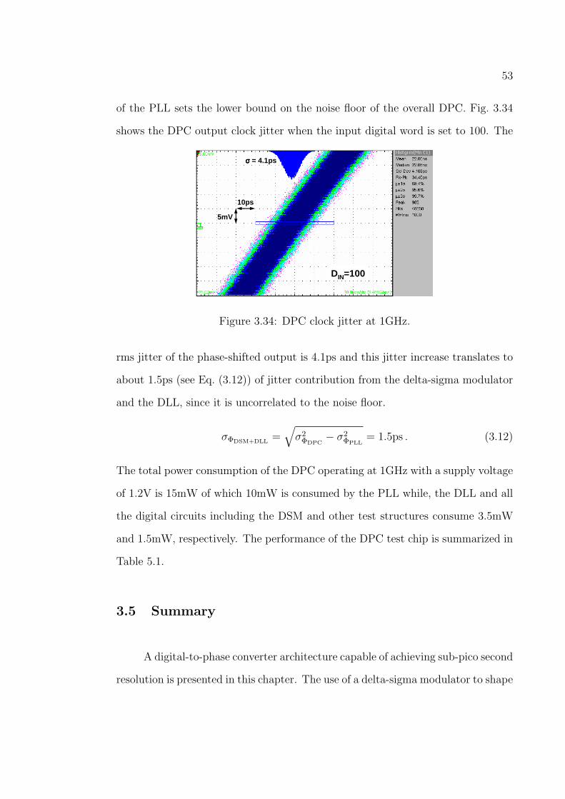
53
of the PLL sets the lower bound on the noise floor of the overall DPC. Fig. 3.34
shows the DPC output clock jitter when the input digital word is set to 100. The
DIN=100
5mV
10ps
σσσσ = 4.1ps
Figure 3.34: DPC clock jitter at 1GHz.
rms jitter of the phase-shifted output is 4.1ps and this jitter increase translates to
about 1.5ps (see Eq. (3.12)) of jitter contribution from the delta-sigma modulator
and the DLL, since it is uncorrelated to the noise floor.
σΦDSM+DLL=
√σ2
ΦDPC− σ2
ΦPLL= 1.5ps . (3.12)
The total power consumption of the DPC operating at 1GHz with a supply voltage
of 1.2V is 15mW of which 10mW is consumed by the PLL while, the DLL and all
the digital circuits including the DSM and other test structures consume 3.5mW
and 1.5mW, respectively. The performance of the DPC test chip is summarized in
Table 5.1.
3.5 Summary
A digital-to-phase converter architecture capable of achieving sub-pico second
resolution is presented in this chapter. The use of a delta-sigma modulator to shape

54
Table 3.2: DPC Performance Summary
Technology 0.13µm CMOS
Supply voltage 1.2V
Operating frequency 0.5GHz – 1.5GHz
DNL/INL±150fs/±12ps @ 0.5GHz
±100fs/±12ps @ 1GHz
Jitter @ 1GHz
PLL : 3.8ps rms
DSM + DLL : 1.5ps rms
Total: 4.1ps rms
Phase span > π radians
Power consumption @ 1GHz
PLL : 10mW
DLL : 3.5mW
Digital : 1.5mW
Total : 15mW
Active die area 0.48mm2
the phase noise to high frequencies and then filtering it out by a low-pass filter
presents an attractive alternative to the design of high resolution digital to phase
converters. The use of a DLL as a phase filter breaks the noise bandwidth tradeoff
of PLLs and facilitates the design of an area and power efficient low-pass filter.
As a result of using noise shaping and phase filtering, this architecture achieves
high resolution that is independent of the operating frequency, rise time, and phase
spacing of the input clock phases.

CHAPTER 4. A HYBRID ANALOG/DIGITAL CLOCK
AND DATA RECOVERY CIRCUIT
In the previous chapter, the design issues associated with de-skewing in
source-synchronous interfaces are addressed. However, a majority of serial sig-
naling systems employ a more economical clocking scheme referred to as embedded
clocking. The most attractive feature of this clocking scheme is that it obviates the
need for a dedicated clock channel. A simplified block diagram of such a system
is depicted in Fig. 4.1. It consists of a transmitter, a channel, and a receiver. The
PLL CDR
D Q
RCK
Figure 4.1: Serial signaling system with embedded clock.
transmitter sends the data to the receiver over a channel, typically a printed circuit
board trace or a co-axial cable. Since the clock is embedded in the data, the re-
ceiver needs to recover both the clock and the data from the incoming serial data.
The design of the receiver is the focus of this chapter. In particular, the design is-
sues of the clock and data recovery (CDR) circuit such as limited frequency/phase
acquisition and tracking range, recovered clock (RCK) jitter, immunity to intrinsic
noise sources are addressed. These issues are first highlighted through a review
of a couple of existing popular CDR architectures and then a new architecture is
presented to overcome these drawbacks.

56
Prior Art – I: Dual-Loop CDR
One of the most commonly used CDR architecture is the dual-loop structure
shown in Fig. 4.2 [13], [14]. It consists of a cascade of two loops, namely, a core
PFD LF VCO
÷NPLL
!!PD FSM ΦΦΦΦint
RCKCDR
DIN
Figure 4.2: Dual-loop CDR.
loop phase-locked loop (PLL) and a peripheral clock and data recovery (CDR)
loop. The PLL generates multiple phases which are used by the phase interpolator
(ΦINT) to introduce a controlled phase shift in the recovered clock (RCK). The
bang-bang phase detector (!!PD) uses the recovered clock to recover the data and
to generate the sign of the phase error between the incoming data and the recovered
clock. The quantized phase error output of the !!PD drives the finite state machine
(FSM) which controls the phase interpolator through a digital control word DIN.
The negative feedback of the CDR loop forces the recovered clock phase to the
middle of the received data. Conceptually, the state machine is implemented as a
simple roll-over integrator to facilitate an unlimited phase shifting capability. This
feature enables plesiochronous clocking between the transmitter and the receiver.
Even though the simplicity of this architecture led to its widespread usage, there
are three main disadvantages with this architecture. They are excessive clock jitter
due to the non-linearity of the phase interpolator, tightly coupled jitter generation
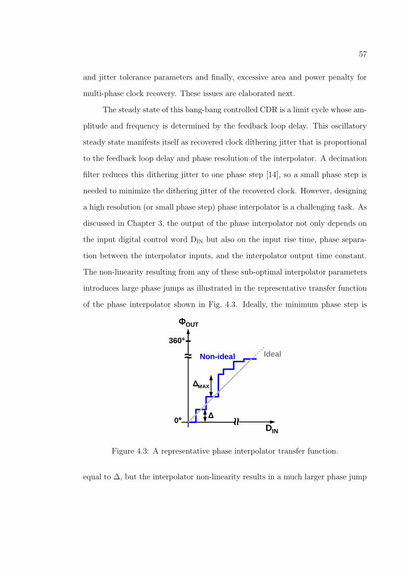
57
and jitter tolerance parameters and finally, excessive area and power penalty for
multi-phase clock recovery. These issues are elaborated next.
The steady state of this bang-bang controlled CDR is a limit cycle whose am-
plitude and frequency is determined by the feedback loop delay. This oscillatory
steady state manifests itself as recovered clock dithering jitter that is proportional
to the feedback loop delay and phase resolution of the interpolator. A decimation
filter reduces this dithering jitter to one phase step [14], so a small phase step is
needed to minimize the dithering jitter of the recovered clock. However, designing
a high resolution (or small phase step) phase interpolator is a challenging task. As
discussed in Chapter 3, the output of the phase interpolator not only depends on
the input digital control word DIN but also on the input rise time, phase separa-
tion between the interpolator inputs, and the interpolator output time constant.
The non-linearity resulting from any of these sub-optimal interpolator parameters
introduces large phase jumps as illustrated in the representative transfer function
of the phase interpolator shown in Fig. 4.3. Ideally, the minimum phase step is
DIN
ΦΦΦΦOUT
360°°°°
0°°°° ≈≈ ≈≈≈≈≈≈
IdealNon-ideal
∆∆∆∆
∆∆∆∆MAX
Figure 4.3: A representative phase interpolator transfer function.
equal to ∆, but the interpolator non-linearity results in a much larger phase jump

58
∆MAX. The recovered clock jitter degradation due to this non-ideal differential
non-linearity (DNL) is illustrated by considering a simplified case in which the
DNL is assumed to be uniformly distributed between ±∆2. The probability density
function (pdf) of the interpolator output phase quantization error in the presence
of DNL (P (ε)) can be calculated by convolving the ideal phase quantization error
pdf, P (εQ), with the DNL pdf, P (εDNL), as illustrated in Fig. 4.4. The variance
Figure 4.4: Calculation of phase error distribution of a phase interpolator withuniformly distributed DNL with a range of ±∆
2.
of the non-linear interpolator output quantization error can then be calculated as
follows:
σ2 =
∫ ∆
−∆
P (ε) · ε2dε =∆2
6>
∆2
12. (4.1)
This equation indicates that the variance of the quantization error is degraded
by a factor of 2 from its ideal value of ∆2
12due to the excess DNL. Therefore, as
mentioned earlier, it is critical to reduce DNL to reduce the dithering jitter. It is
important to note that the integral non-linearity (INL) of the phase interpolator
is not a concern since it is suppressed by the large feedback loop gain.
Overcoming the differential non-linearity of the phase interpolator is a chal-
lenging design task and typically requires considerable area and power. Addi-
tionally, the inherent discrete nature of the FSM controller, introduces discrete
phase jumps at the output of the interpolator output. The jitter caused by these
phase jumps further degrades the receiver performance. In addition to the phase

59
interpolator design issues discussed thus far, this architecture also suffers from a
tightly coupled jitter generation and jitter tolerance parameters. This problem is
explained in detail next.
The small frequency difference between the crystal frequencies of the trans-
mitter and the receiver results in an increasing (decreasing) phase error between
the incoming data and the local clock of the receiver. In order to acquire lock, the
CDR needs to continuously add (or subtract) phase to the recovered clock so as
to reduce the phase error. Consequently, the maximum tolerable frequency error,
referred to as frequency tolerance directly depends on the maximum rate of phase
change and is easily calculated to be,
Maximum frequency tolerance∆f
f≈ Phase step
Phase update interval
= αd · ∆T
DF · TSCK
, (4.2)
where ∆T is the resolution of the phase interpolator, TSCK is the update period of
the state machine, DF is the decimation factor used to reduce the dithering jitter
to one phase step, and αd is the transition density defined with respect to a period
of TSCK. Substituting typical parameters of ∆T = 1UI26 , TSCK = 4UI, DF equal to 8
and αd = 1 where 1UI is the incoming bit period, results in a maximum frequency
tolerance of about 490 parts per million (ppm). In practice, frequency tolerance is
somewhat smaller due to jitter on both the incoming data and the recovered clock.
The inherent non-linear nature of the CDR loop precludes the use of band-
width to determine the tracking properties. However the tracking bandwidth
(f−3dB) defined as the maximum frequency of the input sinusoidal jitter that can
be tracked by the CDR can be calculated to be,
Tracking bandwidth f−3dB ≈ 1
2πΦIN
· αd · ∆T
DF · TSCK
, (4.3)

60
where ΦIN in the amplitude of the input sinusoidal jitter. It is interesting to note
that the tracking bandwidth of the bang-bang CDR depends on the input jitter
amplitude. This is in contrast to linear PLLs whose bandwidth does not depend
on the input amplitude. As indicated by Eqs. (4.2) and (4.3) both the frequency
tolerance and the tracking bandwidth can be improved by increasing the step size
of the interpolator.1 This requirement is contrary to the need for a smaller phase
step to minimize the dithering jitter. In other words, this architecture suffers from
a direct trade-off between jitter generation and jitter tolerance.
Prior Art – II: Phase Averaging CDR
An improved architecture proposed by Larsson [30] increases the phase in-
terpolator resolution and reduces the discrete phase jumps by the use of phase
averaging. The block diagram of the Larsson CDR is shown in Fig. 4.5. In this
PFD LF VCO
÷N
!!PD FSM
ΦΦΦΦint
RCK
DIN
Figure 4.5: CDR with phase averaging phase interpolator.
architecture the interpolator is placed inside the PLL feedback and the voltage
controlled oscillator (VCO) output serves as the recovered clock instead of the
1Increasing frequency tolerance by clocking the state machine at a higher rate is not practicaldue to speed limitations imposed by the process technology.
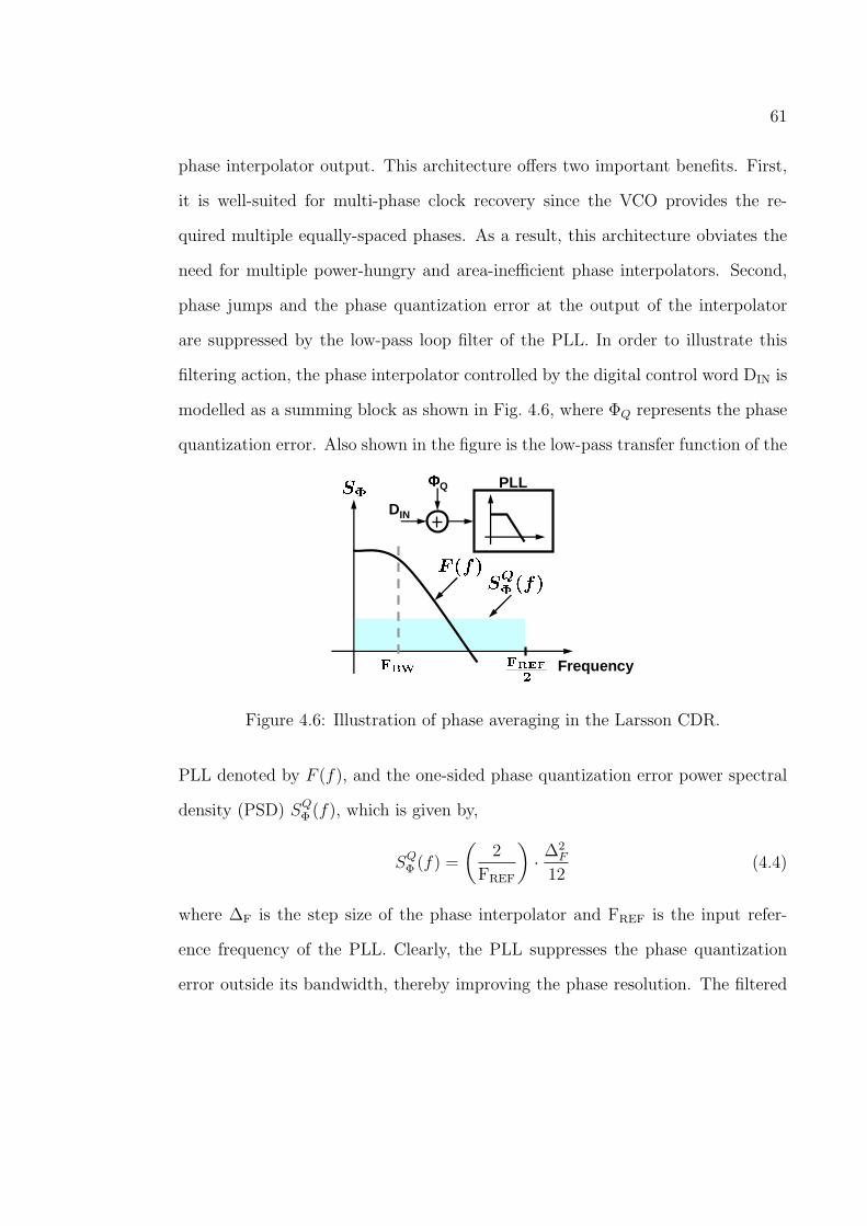
61
phase interpolator output. This architecture offers two important benefits. First,
it is well-suited for multi-phase clock recovery since the VCO provides the re-
quired multiple equally-spaced phases. As a result, this architecture obviates the
need for multiple power-hungry and area-inefficient phase interpolators. Second,
phase jumps and the phase quantization error at the output of the interpolator
are suppressed by the low-pass loop filter of the PLL. In order to illustrate this
filtering action, the phase interpolator controlled by the digital control word DIN is
modelled as a summing block as shown in Fig. 4.6, where ΦQ represents the phase
quantization error. Also shown in the figure is the low-pass transfer function of the
PLLΦΦΦΦQ
DIN
Frequency
Figure 4.6: Illustration of phase averaging in the Larsson CDR.
PLL denoted by F (f), and the one-sided phase quantization error power spectral
density (PSD) SQΦ (f), which is given by,
SQΦ (f) =
(2
FREF
)· ∆2
F
12(4.4)
where ∆F is the step size of the phase interpolator and FREF is the input refer-
ence frequency of the PLL. Clearly, the PLL suppresses the phase quantization
error outside its bandwidth, thereby improving the phase resolution. The filtered

62
quantization error PSD assuming a second-order PLL response can be written as,
SQFΦ (f) = SQ
Φ (f) · |F (f)|2
=∆2
F
6FREF
· |F (f)|2
=∆2
F
6FREF
·∣∣∣∣
ω2n
s2 + 2ζωns + ω2n
∣∣∣∣2
. (4.5)
Due to the suppression of out-of-band noise by the PLL, this architecture simplifies
the design of the phase interpolator. In other words, this architecture allows a
larger phase step size ∆F compared to the conventional phase interpolator step
size ∆ for the same output phase resolution. This improvement in phase resolution
can be shown by calculating the variance of the output phase as shown below:
σ2F =
∫ FREF2
0
SQFΦ (f)df
≈ ∆2F
6FREF
· ωn
8ζ(4.6)
⇒ σF =∆F√12·√
π
2ζ·(
ωn
ωREF
). (4.7)
Using Eq. (4.7), we can conclude that a critically damped PLL with a bandwidth
of one tenth the reference frequency, reduces the root mean square (rms) value of
the output phase quantization error by approximately a factor of 2 compared to
that of the conventional phase interpolator with no phase averaging. This improve-
ment only doubles with every quadrupling of the PLL bandwidth. Consequently,
a very low PLL bandwidth is needed to achieve a high phase resolution using
this approach. This requirement imposes a conflicting requirement on the PLL
bandwidth. As mentioned earlier, the filtering of the phase quantization error of
the interpolator requires a low PLL bandwidth while the suppression of the VCO
phase noise mandates a high bandwidth. This bandwidth conflict reduces the ef-
fectiveness of this architecture. Even though it is possible to design low phase noise
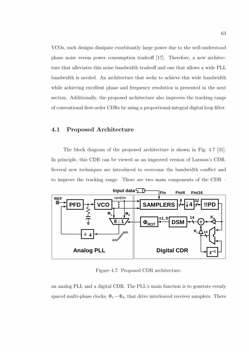
63
VCOs, such designs dissipate exorbitantly large power due to the well-understood
phase noise versus power consumption tradeoff [17]. Therefore, a new architec-
ture that alleviates this noise bandwidth tradeoff and one that allows a wide PLL
bandwidth is needed. An architecture that seeks to achieve this wide bandwidth
while achieving excellent phase and frequency resolution is presented in the next
section. Additionally, the proposed architecture also improves the tracking range
of conventional first-order CDRs by using a proportional-integral digital loop filter.
4.1 Proposed Architecture
The block diagram of the proposed architecture is shown in Fig. 4.7 [31].
In principle, this CDR can be viewed as an improved version of Larsson’s CDR.
Several new techniques are introduced to overcome the bandwidth conflict and
to improve the tracking range. There are two main components of the CDR –
Analog PLL
PFD VCOΦΦΦΦ1 ΦΦΦΦ8
8 : 1
REF
÷ 4
SAMPLERS !!PD4
14
DSM14±1, 0 KP
K I
Input data
8 32
Digital CDR z−−−−1
ΦΦΦΦROT
Fin Fin/4 Fin/16
Figure 4.7: Proposed CDR architecture.
an analog PLL and a digital CDR. The PLL’s main function is to generate evenly
spaced multi-phase clocks, Φ1−Φ8, that drive interleaved receiver samplers. There

64
are eight such clock phases and samplers, four for clock recovery and four for data
recovery. These 8 sampler outputs are down sampled by 4 to ease the speed re-
quirements in the downstream digital circuitry, albeit, at the expense of sacrificing
some tracking bandwidth. A bang-bang phase detector generates 3-level phase
error information by performing early/late detection and a simple majority vote
on the 32 incoming samples. This phase error is filtered by a digital loop filter
consisting of a proportional and an integral path to produce a 14-bit filter output.
As discussed later, the addition of the integral path improves the tracking range
of the CDR. Given the difficulty of implementing a 14-bit phase interpolator with
good linearity, a fully digital CDR controller that takes advantage of the phase
filtering characteristics of the PLL is employed.
The 14-bit loop filter output is quantized to 3-levels (±1, 0) by a second order
delta-sigma modulator (DSM). This 3-level output drives a phase rotator (ΦROT)
which converts the DSM output of −1, 0, and +1 to phase delay, no-change,
and phase advance, respectively. The phase rotator also ensures unlimited phase
capture range and as a result accommodates plesiochronous clocking. The phase
rotator is implemented as a one hot 8-bit circular shift register whose output is used
to select one out of the eight phases of the VCO. The selected phase is fed back to
the PFD after dividing its frequency by four. The low-pass phase transfer function
of the PLL filters the shaped quantization noise of the delta-sigma modulator and,
in combination with the digital control of the CDR loop, appropriately aligns the
VCO clock phases to optimally sample the incoming data. In other words, the
delta-sigma modulator combined with the analog PLL functions as a very high
resolution phase interpolator. Since the phase-interpolation is implemented by
phase selection and filtering, this architecture completely eliminates the problems
of conventional phase interpolators. Let us now look at the phase and frequency

65
resolution achieved by this architecture.
By the virtue of delta-sigma dithering and PLL filtering, ideally, the phase
resolution is given by,
Phase resolution ∆Φ [LSB] =1UI
NPH · 2B(4.8)
=1UI
8 · 214
= 7.6µUI ,
where 1UI is equal to VCO clock period, NPH is the number of VCO phases, and B
is the number of bits in the loop filter output. Quantitatively, there are 2B phases in
between the adjacent phases of the VCO. In practice, however, incomplete filtering
of the shaped noise lowers the resolution from this ideal value.
The frequency resolution is determined by the rate at which the VCO phase
can be updated by the CDR loop. Assuming integral gain to be KI, the CDR loop
can increment/decrement the VCO phase by KI phase steps every update period
TUPDATE. In the proposed architecture the update rate is N times slower than the
VCO clock frequency, where N is the value of the feedback divider. Consequently,
the frequency resolution ∆F can be expressed as,
Frequency resolution ∆F [LSB] =KI ·∆Φ
TUPDATE
(4.9)
=KI
N · NPH · 2B(4.10)
=1
4 · 8 · 214
= 1.9ppm .
Using the parameters from the prototype, better than 2ppm frequency resolution is
achieved. Note that it is also possible to achieve higher phase/frequency resolution
simply by choosing a larger number of loop filter bits at the expense of reduced
tracking bandwidth.

66
The tracking bandwidth of this CDR depends on both the input jitter am-
plitude and frequency as shown earlier by Eq. (4.3). This equation indicates that
if the input jitter has large amplitude or if it varies with high frequency, the CDR
slews, and as a result the output phase can not track the input jitter. In this
architecture, an integral path is added in the loop filter to extend the tracking
bandwidth of the CDR. In the presence of a large phase error, the bang-bang
phase detector is overloaded resulting in an output that has long string of +1’s
or −1’s. The integrator accumulates this continuous stream of identical outputs
and drives the VCO frequency toward frequency lock. In the prototype, with an
integral gain KI equal to one, the integral loop moves the VCO center frequency
in steps of about 2ppm. The tracking range of the CDR, defined as the range of
input frequencies the CDR can track without losing lock is equal to,
Frequency tracking range = ±1
2· 2(WI−1) ·∆F (4.11)
= ±7780ppm .
where WI is the width of the integrator output and ∆F is the frequency resolution.
An extra factor of half in this equation is used to accommodate the fact that only
about half the full-scale range of the delta-sigma modulator is used in this design2.
Using a 14-bit integrator and a frequency resolution of 2ppm the CDR has 7780ppm
of frequency tracking range. This rather large tracking range in valid only if the
input data frequency varies at a slow rate. If the frequency varies at a rate faster
than ∆FTUPDATE
, the integral loop will not be able to move the VCO frequency fast
2The full-scale input to the 3-level DSM overloads the internal quantizer and degrades noiseshaping significantly and may even cause instability. It is a common practice to limit the DSMinput through scaling or by some other means [20].

67
enough to track it. As a result, the integral loop slews and the phase error grows
quadratically, causing the CDR to lose lock eventually.
We have thus far discussed the tracking properties of the proposed CDR.
However, this analysis is based on the assumption that the CDR is in phase lock.
When the CDR is not phase locked, and if the frequency difference between the
incoming data and the local VCO frequency is small, the proportional path will
acquire phase lock with out cycle slipping. In other words, if the phase error
resulting from the frequency error varies at a rate slower than the phase tracking
range of the proportional path, phase lock will be achieved with out cycle slipping.
Therefore, the lock range, defined as the range of frequencies within which the
CDR acquires phase lock without cycle slipping is given by,
Lock range ∆FL = ±KP∆Φ
TUPDATE
(4.12)
= ±240ppm .
KP is the proportional gain and is equal to 128 in the prototype. This lock range
is adequate for the ±100ppm frequency tolerance of commercial crystal oscillators.
The other major advantage of the digital CDR loop is its immunity to process,
voltage and temperature (PVT) variation. The lone mixed-signal block in the CDR
loop that is sensitive to PVT variations is the phase interpolator. However, the
rotating nature of the phase interpolator used in this design, guarantees an average
gain of 2π radians over the total number of control bits as illustrated in Fig. 4.8.
Therefore, if we assume jitter from the incoming data is constant all the other
components of the loop gain are set by digital circuitry, and so the CDR loop
dynamics are immune to PVT variations.

68
DSM14
ΦΦΦΦROT PLL
Phase interpolator
Figure 4.8: Phase interpolator transfer characteristics.
Stability Analysis
There are three feedback loops in the CDR, namely, the phase-locked loop,
the digital clock and data recovery loop, and the combination of these two loops.
The stability of the phase-locked loop is addressed later and is assumed to be
stable for the analysis here. The inherently non-linear nature of the digital clock
and data recovery loop precludes the use of well-known techniques such as Nyquist
plots available for linear systems. However, in the case of non-linear loops, as
described by Walker [32], the stability of the second-order digital CDR loop can
be guaranteed by ensuring the output phase change due to the proportional path
dominates the phase change due to the integral path. Analogous to the damping
factor ζ in linear systems, stability factor ξ is defined as the ratio of the output
phase change due to the proportional path to the output phase change due to the
integral path can be used to quantify the stability of the non-linear CDR loop.
Stability factor ξ =KP ·∆Φ
KI ·∆Φ=
KP
KI
(4.13)

69
A large stability factor (ξ > 100) ensures that the loop dynamics are dominated
by the proportional path, thereby achieving an under damped response.
Even though the stability of a second order CDR loop is guaranteed by a large
ξ, the stability analysis of the proposed CDR is complicated by the interaction of
two feedbacks namely the PLL and the digital CDR loops. Consider the block
diagram of the proposed CDR shown in Fig. 4.9 in which the PLL is depicted
simply as a low-pass filter. From this figure, we can see that the PLL loop is
Input data
SAMPLERS !!PD4
DSMΦΦΦΦROT
PLL
KP
z−−−−1
KI
Figure 4.9: Block diagram of the CDR used for stability analysis.
embedded in the digital CDR loop. Therefore, in order for the PLL to not affect
the CDR stability, the PLL bandwidth should be larger than the maximum rate
of phase change of the digital CDR loop. This condition can be expressed as,
(KP + KI) ·∆Φ
2π · TUPDATE
¿ PLL Bandwidth. (4.14)
Substituting typical parameters from the prototype provided earlier, the PLL
bandwidth needs to be much larger than 60kHz to ensure stability of the com-
plete CDR. Since the bandwidth of the PLL operating with several hundred mega
Hertz update rates is at least a few mega Hertz, the condition in Eq.(4.14) can be
easily met in all practical designs. While Eq.(4.14) defines the lower bound on the
70
PLL bandwidth, the upper bound is set by the filtering requirement to sufficiently
suppress the DSM and the VCO noise. The use of the delta-sigma modulator,
as indicated by the simulation results presented later, allows a larger bandwidth
compared to Larsson’s architecture to filter the VCO noise without exacerbating
the recovered clock jitter due to shaped quantization error.
4.2 Circuit Design
Phase-Locked Loop Design
A major challenge in the design of PLLs in deep sub-micron processes is the
degraded noise sensitivity due to the increase in the gain of the voltage controlled
oscillator (VCO). The continued down scaling of CMOS processes to deep sub-
micron dimensions provides transistors with very high unity current gain frequency
fT . However, this down scaling requires similar shrinking of the supply voltage to
ensure transistor reliability. As a result of these two scaling trends, the voltage
controlled ring oscillators designed in deep sub-micron processes and operating
over a wide frequency range have large gain. In such oscillators, a reduction in
gain comes only at the expense of a reduced operating frequency range. The block
diagram of the split-tuned PLL that breaks the tradeoff between the operating
range and the VCO gain is shown in Fig. 4.10. This architecture offers the benefits
of both a wide operating range and a reduced VCO gain. The PLL consists of
a phase frequency detector (PFD), a level shifter (SHFT), a charge pump (CP),
a loop filter consisting of an RC network, a Gm − CI integrator, two voltage-to-
current (V2I) converters, a 4-stage split-tuned current controlled ring oscillator
(CCO) controlled by separate high-gain coarse and low-gain fine inputs, and a
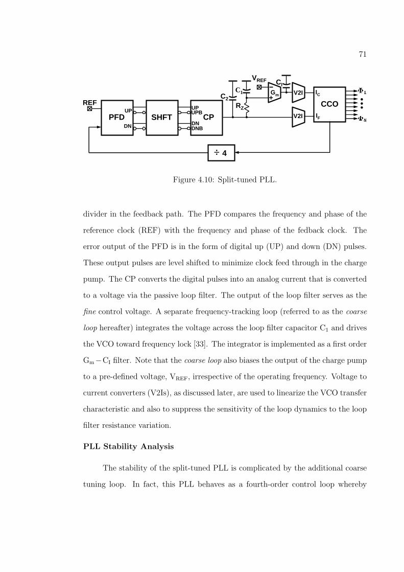
71
PFD SHFT CPUP
DN
UP
DN
UPB
DNB
+ V2I
V2I
Gm
CCO
IC
IF
C2
C1
RZ
CI
÷ 4
REF
VREF
Figure 4.10: Split-tuned PLL.
divider in the feedback path. The PFD compares the frequency and phase of the
reference clock (REF) with the frequency and phase of the fedback clock. The
error output of the PFD is in the form of digital up (UP) and down (DN) pulses.
These output pulses are level shifted to minimize clock feed through in the charge
pump. The CP converts the digital pulses into an analog current that is converted
to a voltage via the passive loop filter. The output of the loop filter serves as the
fine control voltage. A separate frequency-tracking loop (referred to as the coarse
loop hereafter) integrates the voltage across the loop filter capacitor C1 and drives
the VCO toward frequency lock [33]. The integrator is implemented as a first order
Gm−CI filter. Note that the coarse loop also biases the output of the charge pump
to a pre-defined voltage, VREF, irrespective of the operating frequency. Voltage to
current converters (V2Is), as discussed later, are used to linearize the VCO transfer
characteristic and also to suppress the sensitivity of the loop dynamics to the loop
filter resistance variation.
PLL Stability Analysis
The stability of the split-tuned PLL is complicated by the additional coarse
tuning loop. In fact, this PLL behaves as a fourth-order control loop whereby

72
ensuring unconditional stability is more difficult compared to conventional third-
order PLLs. However, it is still possible to perform a stability analysis using
conventional methods. The loop gain of the PLL can be expressed as the sum of
the loop gains of the coarse and the fine paths as shown below,
Fine loop gain LGF(s) =KF
vcoIcp2πN
s + 1RZC1
C2 s2
(s + 1
RZ
C1C2
C1+C2
) 1(
1 + sωF
) (4.15)
Coarse loop gain LGC(s) =KC
vcoIcp2πN
1
C2 s2
(s + 1
RZ
C1C2
C1+C2
) Gm
CIs
1(1 + s
ωC
)(4.16)
PLL loop gain LG(s) = LGF(s) + LGC(s) , (4.17)
where Icp is the charge-pump bias current, N is the feedback divider ratio, ωF and
ωC are the bandwidths of fine, and coarse V2Is respectively, KCvco and KF
vco are the
coarse and fine gains of the VCO3, respectively. Eq. (4.16) assumes the output
impedance of the Gm stage is infinite for simplicity. In practice, the finite output
impedance moves the integrator pole from DC to a slightly higher frequency. Note
that the fine loop gain shown in Eq. (4.15) is same as the loop gain of conventional
third-order PLLs. By designing the cross-over frequency of the coarse loop to be
much smaller than the zero frequency (FZ = 12πRZC1
), the effect of coarse loop
on the loop phase margin can be suppressed. In this case, the loop dynamics of
the proposed PLL are determined solely by the fine loop. The design procedure
involves choosing the fine loop parameters to meet the bandwidth and phase margin
requirements and then adjusting the coarse loop parameters, Gm and CI, to reduce
the effect of the coarse loop on the overall loop dynamics.
3The VCO is viewed as a combination of the V2I and the CCO. The gain of the VCO is theproduct of the gains of the V2I and the CCO.
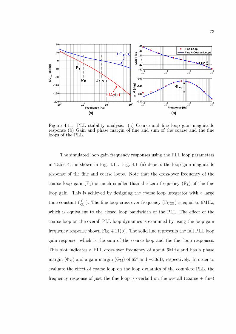
73
105
106
107
108
-200
-160
-120
-80
-40
0
40
80
Frequency [Hz]
|LG
F,C
(s)|
[d
B]
105
106
107
108
-40
-20
0
20
40
60
|LG
(s)|
[d
B]
105
106
107
108
-220
-180
-140
-100
Frequency [Hz]
∠∠ ∠∠ L
G [
deg
]
Fine LoopFine + Coarse Loops
(a) (b)
Figure 4.11: PLL stability analysis: (a) Coarse and fine loop gain magnituderesponse (b) Gain and phase margin of fine and sum of the coarse and the fineloops of the PLL.
The simulated loop gain frequency responses using the PLL loop parameters
in Table 4.1 is shown in Fig. 4.11. Fig. 4.11(a) depicts the loop gain magnitude
response of the fine and coarse loops. Note that the cross-over frequency of the
coarse loop gain (F1) is much smaller than the zero frequency (FZ) of the fine
loop gain. This is achieved by designing the coarse loop integrator with a large
time constant ( CI
Gm). The fine loop cross-over frequency (FUGB) is equal to 6MHz,
which is equivalent to the closed loop bandwidth of the PLL. The effect of the
coarse loop on the overall PLL loop dynamics is examined by using the loop gain
frequency response shown Fig. 4.11(b). The solid line represents the full PLL loop
gain response, which is the sum of the coarse loop and the fine loop responses.
This plot indicates a PLL cross-over frequency of about 6MHz and has a phase
margin (ΦM) and a gain margin (GM) of 65 and −30dB, respectively. In order to
evaluate the effect of coarse loop on the loop dynamics of the complete PLL, the
frequency response of just the fine loop is overlaid on the overall (coarse + fine)

74
Table 4.1: PLL loop parameters.
PLL Bandwidth (FUGB) 6MHz
Phase margin (ΦM) 65
Gain margin (GM) −30dB
Charge-pump current (Icp) 100µA
Filter resistor (RZ) 8KΩ
Filter capacitor (C1) 19pF
Ripple capacitor (C2) 0.6pF
Coarse VCO gain (KCvco) 1.2GHz/V
Fine VCO gain (KFvco) 0.2GHz/V
Coarse V2I bandwidth (2πωC) 4MHz/V
Fine V2I bandwidth (2πωF) 100MHz/V
Feedback divider ratio (N) 4
Transconductance (Gm) 5µA/V
Integrator capacitor (CI) 120pF
loop response in Fig. 4.11(b). This plot indicates negligible gain and phase margin
degradation of the overall loop due to the coarse loop.
PLL Noise Analysis
Noise is an important design concern in a phase-locked loop. The intrinsic
and extrinsic noise sources such as thermal/flicker noise and the shaped quan-
tization error of the DSM, respectively, along with the interference from supply
and substrate noise appear as phase noise of the output clock phases. This phase
noise manifests itself as the uncertainty of the zero crossing times of the output
clocks, referred to as clock jitter, and severely affects the bit error ratio of the

75
receiver. Hence, it is of paramount importance to minimize the PLL output phase
noise. The small-signal model of the PLL depicting all the intrinsic noise sources
is shown in Fig. 4.12. Each of the noise sources are represented by their power
Figure 4.12: Small-signal noise model of the PLL including the DSM noise.
spectral densities (PSD). For example, the current noise PSD of the charge pump
output current and the voltage noise PSD of the loop filter resistor are represented
by SiCPand SvRz
, respectively. The feedback network noise PSD, SΦFB, represents
the noise of the divider, the phase-selecting multiplexer, and the buffers used at
the output of mux. LFF(s) and LFC(s) are the loop filter transfer functions of the
fine and coarse loops and are given by,
LFF(s) =s + 1
RZC1
C2 s2
(s + 1
RZ
C1C2
C1+C2
) (4.18)
LFC(s) =1
C2 s2
(s + 1
RZ
C1C2
C1+C2
) . (4.19)
The noise sources depicted in Fig. 4.12 are shaped differently by the PLL
loop, determined by the noise transfer functions (NTF) associated with each of

76
the noise sources. The NTFs of all the noise sources are given below,
NTFFB(s) =ΦOUT(s)
ΦFB(s)=
N · LG(s)
1 + LG(s)(4.20)
NTFCP(s) =ΦOUT(s)
iCP(s)=
2π
ICP
· NTFFB(s) (4.21)
NTFDSM(s) =ΦOUT(s)
ΦDSM(s)=
1
N· NTFFB(s) (4.22)
NTFRZ(s) =
ΦOUT(s)
vRZ(s)
=
KFVCO
s
1 + LG(s)(4.23)
NTFRZ(s) =
ΦOUT(s)
vGM(s)
=
KCVCO
s
1 + LG(s)(4.24)
NTFVCO(s) =ΦOUT(s)
ΦVCO(s)=
1
1 + LG(s). (4.25)
These NTFs illustrate the noise bandwidth tradeoff in PLLs. For example, the
charge pump noise is low-pass filtered and the VCO phase noise is high-pass shaped,
both with a bandwidth equal to that of the PLL. In other words, increasing the
bandwidth of the PLL exacerbates the charge pump noise and suppresses VCO
noise, and vice versa. In view of this tradeoff, the PLL bandwidth is carefully
optimized through iterative simulations, to minimize the total output phase noise,
STOTALΦOUT
(s) = SiCPΦOUT
(s) + SFBΦOUT
(s) + SvRZΦOUT
(s) + SvGMΦOUT
(s)
+SΦVCOΦOUT
(s) + SΦDSMΦOUT
(s) , (4.26)
where each of the individual terms are equal to the product of noise PSD with the
squared magnitude of the corresponding NTF. For example, SiCPΦOUT
is calculated
as follows:
SiCPΦOUT
= SiCP· |NTFCP(s)|2 . (4.27)
The final result obtained from the noise bandwidth optimization simulations is
presented in Fig. 4.13. The PLL output phase noise STOTALΦOUT
(s) is shown by the thick
solid line. Other lines indicate the noise contribution from individual noise sources
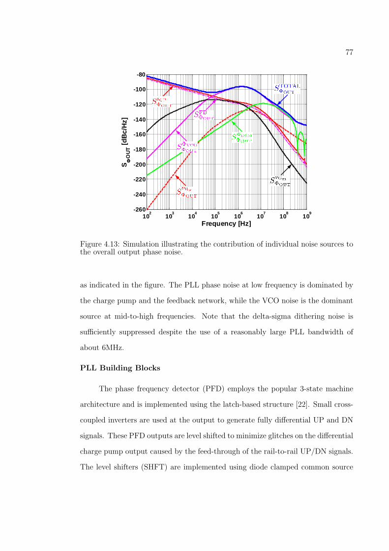
77
102
103
104
105
106
107
108
109
-260
-240
-220
-200
-180
-160
-140
-120
-100
-80
Frequency [Hz]
SΦΦ ΦΦ
OU
T [
dB
c/H
z]
Figure 4.13: Simulation illustrating the contribution of individual noise sources tothe overall output phase noise.
as indicated in the figure. The PLL phase noise at low frequency is dominated by
the charge pump and the feedback network, while the VCO noise is the dominant
source at mid-to-high frequencies. Note that the delta-sigma dithering noise is
sufficiently suppressed despite the use of a reasonably large PLL bandwidth of
about 6MHz.
PLL Building Blocks
The phase frequency detector (PFD) employs the popular 3-state machine
architecture and is implemented using the latch-based structure [22]. Small cross-
coupled inverters are used at the output to generate fully differential UP and DN
signals. These PFD outputs are level shifted to minimize glitches on the differential
charge pump output caused by the feed-through of the rail-to-rail UP/DN signals.
The level shifters (SHFT) are implemented using diode clamped common source
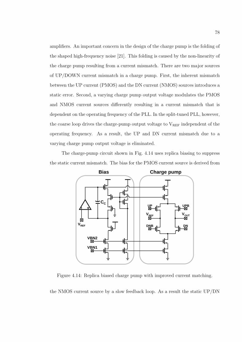
78
amplifiers. An important concern in the design of the charge pump is the folding of
the shaped high-frequency noise [21]. This folding is caused by the non-linearity of
the charge pump resulting from a current mismatch. There are two major sources
of UP/DOWN current mismatch in a charge pump. First, the inherent mismatch
between the UP current (PMOS) and the DN current (NMOS) sources introduces a
static error. Second, a varying charge pump output voltage modulates the PMOS
and NMOS current sources differently resulting in a current mismatch that is
dependent on the operating frequency of the PLL. In the split-tuned PLL, however,
the coarse loop drives the charge-pump output voltage to VREF independent of the
operating frequency. As a result, the UP and DN current mismatch due to a
varying charge pump output voltage is eliminated.
The charge-pump circuit shown in Fig. 4.14 uses replica biasing to suppress
the static current mismatch. The bias for the PMOS current source is derived from
UP
DNB
UPB
DN
VREF VOUT
+
VREF
CC
VBN2
VBN1
Bias Charge pump
Figure 4.14: Replica biased charge pump with improved current matching.
the NMOS current source by a slow feedback loop. As a result the static UP/DN

79
current mismatch is suppressed by the loop gain of the feedback. The Gm − CI
integrator in Fig. 4.10 is implemented using a folded-cascode transconductor and
a poly-poly integrating capacitor CI. As mentioned earlier, a large coarse loop
integrator time constant, CI
Gm, is needed to ensure stability and to suppress the effect
of the coarse loop on the PLL loop dynamics. In order to reduce the area penalty
needed by a large capacitor CI, the transconductor Gm needs to be minimized.
The folded-cascode transconductor employs weak positive feedback to reduce Gm
to about 5µA/V with a reasonable bias current of 5µA. The simulated output
impedance of the transconductor is roughly 72MΩ.
Both the coarse and fine voltages are converted to current signals using V2I
converters shown in Fig. 4.15. The coarse V2I converter shown in Fig. 4.15(a) uses
IC+
VC
RC
VREF
VB
VF
RF
IF
(a) (b)
Figure 4.15: V2I circuits: (a) Coarse V2I (b) Fine V2I.
negative feedback to maximize the operating frequency range of the PLL. The
single-stage folded-cascode feedback amplifier employs complementary differential
input pairs to achieve a rail-to-rail input common mode range and nearly rail-to-
rail output swing. Since the amplifier bandwidth does not influence the coarse
loop operation, low bias currents are used to reduce power consumption. On the
other hand, the V2I converter in the fine loop needs to have a large bandwidth to
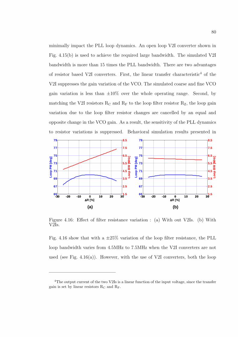
80
minimally impact the PLL loop dynamics. An open loop V2I converter shown in
Fig. 4.15(b) is used to achieve the required large bandwidth. The simulated V2I
bandwidth is more than 15 times the PLL bandwidth. There are two advantages
of resistor based V2I converters. First, the linear transfer characteristic4 of the
V2I suppresses the gain variation of the VCO. The simulated coarse and fine VCO
gain variation is less than ±10% over the whole operating range. Second, by
matching the V2I resistors RC and RF to the loop filter resistor RZ, the loop gain
variation due to the loop filter resistor changes are cancelled by an equal and
opposite change in the VCO gain. As a result, the sensitivity of the PLL dynamics
to resistor variations is suppressed. Behavioral simulation results presented in
-30 -20 -10 0 10 20 3065
67
69
71
73
75
77
79
Lo
op
PM
[d
eg
]
-30 -20 -10 0 10 20 301.5
2.5
3.5
4.5
5.5
6.5
7.5
8.5
Lo
op
BW
[M
Hz]
∆∆∆∆R [%]-30 -20 -10 0 10 20 30
65
67
69
71
73
75
77
79
Lo
op
PM
[d
eg
]
-30 -20 -10 0 10 20 301.5
2.5
3.5
4.5
5.5
6.5
7.5
8.5
Lo
op
BW
[M
Hz]
∆∆∆∆R [%]
(a) (b)
Figure 4.16: Effect of filter resistance variation : (a) With out V2Is. (b) WithV2Is.
Fig. 4.16 show that with a ±25% variation of the loop filter resistance, the PLL
loop bandwidth varies from 4.5MHz to 7.5MHz when the V2I converters are not
used (see Fig. 4.16(a)). However, with the use of V2I converters, both the loop
4The output current of the two V2Is is a linear function of the input voltage, since the transfergain is set by linear resistors RC and RF.

81
bandwidth and phase margin remain constant over a broad range of loop filter
resistance variations (see Fig. 4.16(b)).
A four stage split-tuned ring oscillator composed of pseudo-differential delay
cells shown in Fig. 5.7 is used in this design [28]. The delay cell is a current
IF
IC
ΦΦΦΦ1 ΦΦΦΦ2 ΦΦΦΦ3 ΦΦΦΦ4ΦΦΦΦ5 ΦΦΦΦ6 ΦΦΦΦ7 ΦΦΦΦ8
IF
IC 4X
1X
Figure 4.17: Split-tuned current controlled oscillator.
starved inverter in which the current source is split into a 4X device and a 1X
device controlled by the coarse and fine control signals, respectively. The simulated
coarse and fine gains of the VCO are 1200MHz/V and 200MHz/V, respectively,
and the operating range is 50MHz – 1300MHz. This wide tuning range is made
possible by the ability to reduce the charging current to extremely small levels.
A close look at the delay cell reveals that the effective output load capacitor (not
shown explicitly in Fig. 5.7) is charged by the controllable current source, while it is
discharged by the combination of the discharging current determined by the input
voltage and the strength of the cross-coupled latch. Typically, at low-to-medium
operating frequencies, the delay cell output is pulled down faster than being pulled
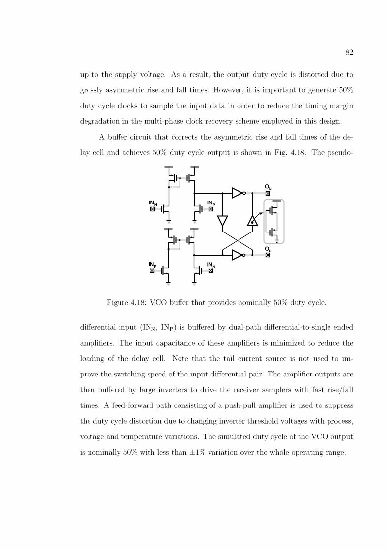
82
up to the supply voltage. As a result, the output duty cycle is distorted due to
grossly asymmetric rise and fall times. However, it is important to generate 50%
duty cycle clocks to sample the input data in order to reduce the timing margin
degradation in the multi-phase clock recovery scheme employed in this design.
A buffer circuit that corrects the asymmetric rise and fall times of the de-
lay cell and achieves 50% duty cycle output is shown in Fig. 4.18. The pseudo-
INN INP
INP INN
ON
OP
Figure 4.18: VCO buffer that provides nominally 50% duty cycle.
differential input (INN, INP) is buffered by dual-path differential-to-single ended
amplifiers. The input capacitance of these amplifiers is minimized to reduce the
loading of the delay cell. Note that the tail current source is not used to im-
prove the switching speed of the input differential pair. The amplifier outputs are
then buffered by large inverters to drive the receiver samplers with fast rise/fall
times. A feed-forward path consisting of a push-pull amplifier is used to suppress
the duty cycle distortion due to changing inverter threshold voltages with process,
voltage and temperature variations. The simulated duty cycle of the VCO output
is nominally 50% with less than ±1% variation over the whole operating range.

83
Digital Clock and Data Recovery Loop Design
The detailed block diagram of the multi-phase digital clock and data recovery
loop is shown in Fig. 4.19. The PLL based phase interpolator provides 8 equally
8-to-16DEMUXDATA/EDGE
SAMPLERS
16-to-32DEMUX
8 16!!PD
32 MAJORITYVOTE
16
÷ 2
<< 714
D Q
REGISTER
÷ 2
PHASEROTATOR
PHASE INTERPOLATOR
PLL
28
DSM
2
14
SCK
Figure 4.19: CDR block diagram.
spaced clock phases at quarter data rate to the four data samplers and four edge
samplers. As a result of this multi-phase approach the maximum on-chip clock
frequency is reduced to quarter of the input data rate. The 8 samples, four edge and
four data, are further de-multiplexed to 32 samples by two stages of de-multiplexers
operating at one half and one quarter of the VCO frequency. The following digital
circuits are also clocked with this slow quarter rate recovered clock SCK (250MHz
at 4Gbps operation). The 32 samples go through 16 early/late decoders to generate
16 early/late/hold signals, which are then resolved by a majority vote to produce
a 3-level phase error signal. The phase error is then filtered by the digital loop
filter with a proportional and an integral gain of 128 and 1 respectively. A 14-bit
accumulator is used to implement the integral control and the proportional gain
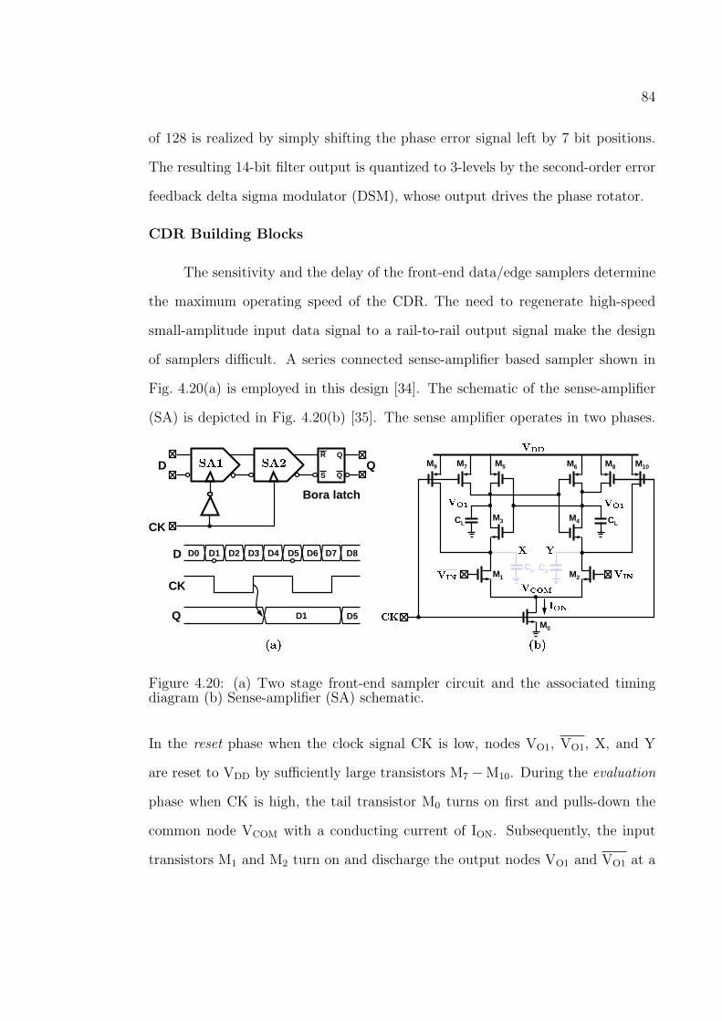
84
of 128 is realized by simply shifting the phase error signal left by 7 bit positions.
The resulting 14-bit filter output is quantized to 3-levels by the second-order error
feedback delta sigma modulator (DSM), whose output drives the phase rotator.
CDR Building Blocks
The sensitivity and the delay of the front-end data/edge samplers determine
the maximum operating speed of the CDR. The need to regenerate high-speed
small-amplitude input data signal to a rail-to-rail output signal make the design
of samplers difficult. A series connected sense-amplifier based sampler shown in
Fig. 4.20(a) is employed in this design [34]. The schematic of the sense-amplifier
(SA) is depicted in Fig. 4.20(b) [35]. The sense amplifier operates in two phases.
M9
M1
Cp
CLM3
M5M7
Cp
M10
M2
CLM4
M6 M8
R Q
S QD
CK
Q
D0 D1 D2 D3 D4 D5 D6 D7 D8
D1 D5
D
CK
Q
Bora latch
M0
Figure 4.20: (a) Two stage front-end sampler circuit and the associated timingdiagram (b) Sense-amplifier (SA) schematic.
In the reset phase when the clock signal CK is low, nodes VO1, VO1, X, and Y
are reset to VDD by sufficiently large transistors M7 −M10. During the evaluation
phase when CK is high, the tail transistor M0 turns on first and pulls-down the
common node VCOM with a conducting current of ION. Subsequently, the input
transistors M1 and M2 turn on and discharge the output nodes VO1 and VO1 at a

85
rate determined the input differential voltage. For example, with a positive input
voltage difference (VIN > VIN), VOUT discharges at a faster rate and when this
voltage reaches VDD−Vthp, M5 turns on and initiates the regeneration due to the
positive feedback of the latch. As a result, the output voltage difference grows
exponentially until VO1 and VO1 reach VDD and 0 respectively. In this steady
state, M3 and M6 turn off and avoid static power dissipation.
The data evaluation time and sensitivity are important performance metrics
of the data/edge samplers. Series connected sense amplifiers (Fig. 4.20(a)) increase
the data evaluation time to 4-bit periods by decoupling the evaluation periods of
the two sense amplifiers SA1 and SA2. The sensitivity is improved by minimiz-
ing the offset of SA1 through the choice of a reasonably large input devices and
careful layout that reduces the mismatch of both the transistors and parasitics
capacitances CP and CL. Additionally, the input devices of SA2 are scaled down
to improve the regeneration speed of SA1 and a symmetric Bora latch [36] is used
to minimize hysteresis in the second stage sense amplifier.
The 8 sampler outputs are demultiplexed to produce 16 data samples and 16
edge samples that are processed by a set of 16 bang-bang (!!) phase detectors [37]
as shown in Fig. 4.21. The intermediate edge sample (ES[j]) between two adjacent
data samples (D[j], D[j+1]) is used to determine whether clock is early(E[j]) or
late(L[j]). In the absence of a data transition, the hold (H[j]) signal is activated.
To reduce the complexity of the digital loop filter, these 16 sets of early/late/hold
signals are resolved by a majority vote to produce 3-level phase error signal.
The delta sigma modulator (DSM) used in this design employs a single-loop
second-order error feedback architecture with a 3-level internal quantizer [20]. The
3-level DSM output drives the phase rotator which is implemented by the circular
shift register (CSR) shown in Fig. 4.22. On power-up, CSR is reset to a 2-hot state
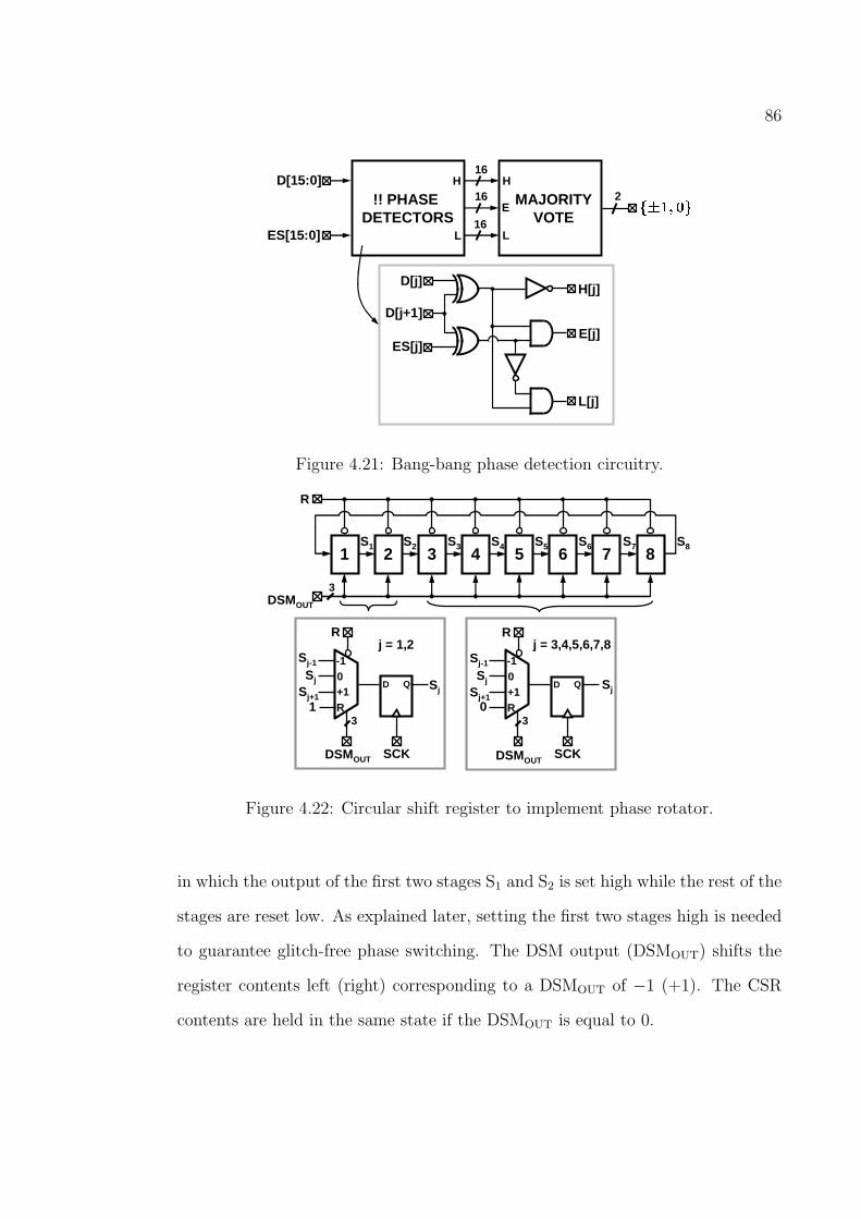
86
!! PHASE DETECTORS
MAJORITYVOTE
E[j]
L[j]
H[j]D[j]
D[j+1]
ES[j]
ES[15:0]
D[15:0]
16
16
16H
L
H
L
E2
Figure 4.21: Bang-bang phase detection circuitry.
3 4 5 6 721 8
DSMOUT
R
3
S1 S2 S4S3 S5 S6 S7 S8
D Q
-10+1R
SCK
R
30
Sj
Sj
Sj-1
Sj+1
j = 3,4,5,6,7,8
D Q
-10+1R
SCK
R
31
Sj
Sj-1
Sj+1Sj
j = 1,2
DSMOUT DSMOUT
Figure 4.22: Circular shift register to implement phase rotator.
in which the output of the first two stages S1 and S2 is set high while the rest of the
stages are reset low. As explained later, setting the first two stages high is needed
to guarantee glitch-free phase switching. The DSM output (DSMOUT) shifts the
register contents left (right) corresponding to a DSMOUT of −1 (+1). The CSR
contents are held in the same state if the DSMOUT is equal to 0.
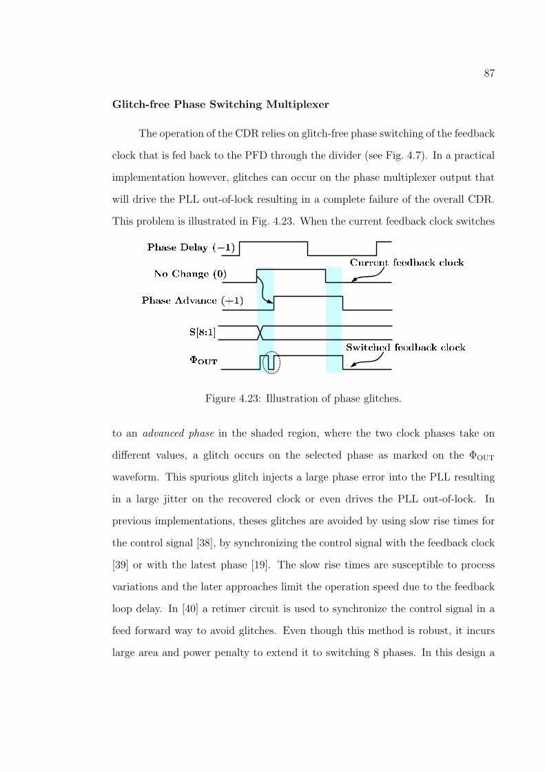
87
Glitch-free Phase Switching Multiplexer
The operation of the CDR relies on glitch-free phase switching of the feedback
clock that is fed back to the PFD through the divider (see Fig. 4.7). In a practical
implementation however, glitches can occur on the phase multiplexer output that
will drive the PLL out-of-lock resulting in a complete failure of the overall CDR.
This problem is illustrated in Fig. 4.23. When the current feedback clock switches
Figure 4.23: Illustration of phase glitches.
to an advanced phase in the shaded region, where the two clock phases take on
different values, a glitch occurs on the selected phase as marked on the ΦOUT
waveform. This spurious glitch injects a large phase error into the PLL resulting
in a large jitter on the recovered clock or even drives the PLL out-of-lock. In
previous implementations, theses glitches are avoided by using slow rise times for
the control signal [38], by synchronizing the control signal with the feedback clock
[39] or with the latest phase [19]. The slow rise times are susceptible to process
variations and the later approaches limit the operation speed due to the feedback
loop delay. In [40] a retimer circuit is used to synchronize the control signal in a
feed forward way to avoid glitches. Even though this method is robust, it incurs
large area and power penalty to extend it to switching 8 phases. In this design a
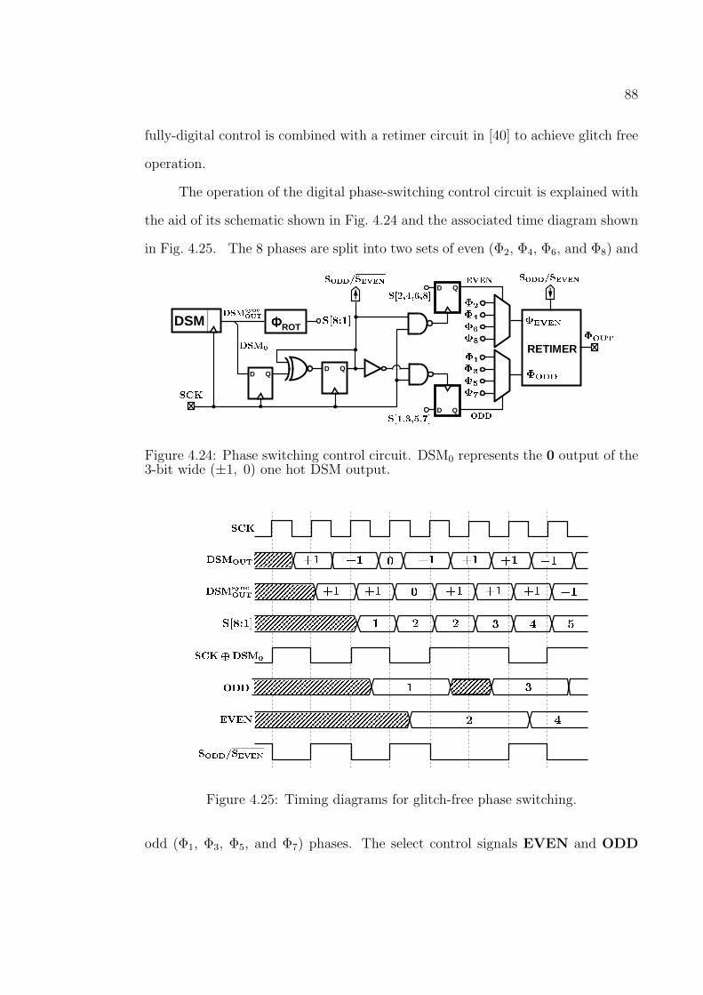
88
fully-digital control is combined with a retimer circuit in [40] to achieve glitch free
operation.
The operation of the digital phase-switching control circuit is explained with
the aid of its schematic shown in Fig. 4.24 and the associated time diagram shown
in Fig. 4.25. The 8 phases are split into two sets of even (Φ2, Φ4, Φ6, and Φ8) and
D Q
DSM
D Q
D Q
D Q
RETIMER
ΦΦΦΦROT
Figure 4.24: Phase switching control circuit. DSM0 represents the 0 output of the3-bit wide (±1, 0) one hot DSM output.
Figure 4.25: Timing diagrams for glitch-free phase switching.
odd (Φ1, Φ3, Φ5, and Φ7) phases. The select control signals EVEN and ODD

89
are generated so that the phases in one set are switched when the output phase is
selected from the other set. Consequently, even if glitches occur during this phase
transition at the output of the unselected multiplexer, they do not appear at the
final output ΦOUT. One of the outputs of the two multiplexers is then selected
by a glitch-free retimer circuit based on the control signal SODD/SEVEN. In case
the DSM output is either +1 or −1, SODD/SEVEN simply alternates between 0
and 1 and therefore can be simply generated by dividing the clock (SCK) by 2. In
order to account for zero DSM output, an additional exclusive NOR gate is used
to realize the conditional divide by 2 operation. Further, the clocked nand gates
synchronize the SODD/SEVEN to the negative edge of the clock.
4.3 Experimental Results
The test chip was fabricated in a 0.18µm CMOS process and the die photo
is shown in Fig. 4.26. Large portion of the PLL is occupied by the capacitor of
the GM−CI integrator. The active die area is 0.8mm2. The die was packaged in a
standard 64-pin TQFP plastic package. The packaged chip is attached to a 4-layer
test board through a clamp screw that is used to mechanically press the package
to force its leads to contact solder pads on the test board.
The recovered quarter rate data and clock with a 2Gbps input data is shown
in Fig. 4.27. The measured bit error rate (BER) is better than 10−12. The measured
tracking range of the CDR when the PLL reference clock is modulated with a
20kHz triangular wave is better than ±2500 ppm. This frequency tracking range
is measured without any degradation of the BER from its nominal value of 10−12.
The jitter histogram of the PLL operating at 500MHz shown in Fig. 4.28, indicates
an rms clock jitter of 5.3ps. When the CDR loop is turned on, the recovered clock
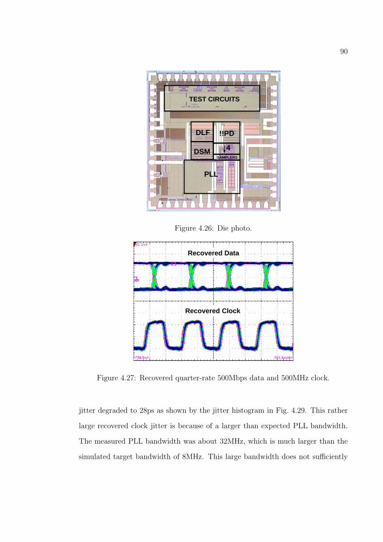
90
PLL
DLF
DSM
!!PD
SAMPLERS
4
TEST CIRCUITS
Figure 4.26: Die photo.
Recovered Data
Recovered Clock
Figure 4.27: Recovered quarter-rate 500Mbps data and 500MHz clock.
jitter degraded to 28ps as shown by the jitter histogram in Fig. 4.29. This rather
large recovered clock jitter is because of a larger than expected PLL bandwidth.
The measured PLL bandwidth was about 32MHz, which is much larger than the
simulated target bandwidth of 8MHz. This large bandwidth does not sufficiently
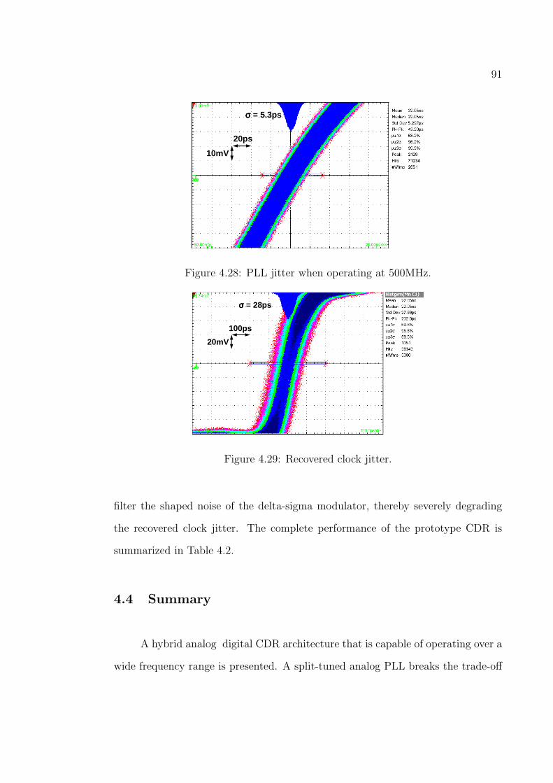
91
10mV
20ps
σσσσ = 5.3ps
Figure 4.28: PLL jitter when operating at 500MHz.
20mV
100ps
σσσσ = 28ps
Figure 4.29: Recovered clock jitter.
filter the shaped noise of the delta-sigma modulator, thereby severely degrading
the recovered clock jitter. The complete performance of the prototype CDR is
summarized in Table 4.2.
4.4 Summary
A hybrid analog digital CDR architecture that is capable of operating over a
wide frequency range is presented. A split-tuned analog PLL breaks the trade-off
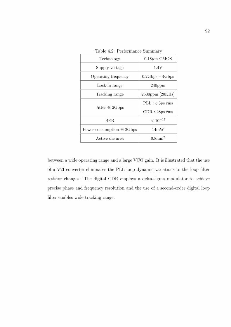
92
Table 4.2: Performance Summary
Technology 0.18µm CMOS
Supply voltage 1.4V
Operating frequency 0.2Gbps – 4Gbps
Lock-in range 240ppm
Tracking range 2500ppm [20KHz]
Jitter @ 2GbpsPLL : 5.3ps rms
CDR : 28ps rms
BER < 10−12
Power consumption @ 2Gbps 14mW
Active die area 0.8mm2
between a wide operating range and a large VCO gain. It is illustrated that the use
of a V2I converter eliminates the PLL loop dynamic variations to the loop filter
resistor changes. The digital CDR employs a delta-sigma modulator to achieve
precise phase and frequency resolution and the use of a second-order digital loop
filter enables wide tracking range.

CHAPTER 5. A DIGITAL CLOCK AND DATA
RECOVERY CIRCUIT
The ever increasing demand for large off-chip I/O bandwidth requires inte-
gration of many serial links on a large digital chip. These serial links need to be
low-power, easily portable to different process technologies, and should operate
reliably in noisy environments. A clock and data recovery (CDR) circuit is an
integral component of these serial links and is the focus of this chapter. Mod-
ern CDRs are commonly implemented using analog phase-locked loops (PLLs) as
shown in Fig. 5.1 [41]. A bang-bang phase detector (!!PD) determines the sign of
CP!!PD±1,0
±Icp,0
-1 →→→→ EARLY0 →→→→ NO TRANSITION+1 →→→→ LATE
R
C
RCK
VCO
VF
VC
Figure 5.1: Conventional analog CDR.
the phase error between the incoming data and the recovered clock (RCK). The 3-
level (early/late/no transition) phase error is converted to a current by the charge
pump (CP) and filtered by the RC loop filter. The filtered control voltage (VF )
drives the voltage controlled oscillator (VCO) toward phase lock. The use of a !!PD
limits the pull-in range of the CDR to a few thousand parts per million (ppm) thus
requiring a frequency acquisition aid. There are several digital frequency-locking
loop (FLL) architectures in the literature [42] that can be used to drive the coarse
control voltage (VC) of the VCO to bring its frequency to within the pull-in range
of the CDR.

94
Even though these analog CDRs offer good performance, they do not easily
port to different technologies, require extra mask steps to implement the passive
elements, are susceptible to leakage, and prohibit quick production-level testing.
Techniques to implement a digital CDR to overcome some of the drawbacks associ-
ated with analog CDRs are presented in this chapter. Section 5.1 presents a simple
digital CDR architecture and identifies the issues associated with it. A new archi-
tecture that overcomes the issues of the simple digital architecture is presented in
Section 5.2. A linearized analysis of the CDR loop and the circuit design details
are discussed in Section 5.3 and Section 5.4, respectively. Finally, the experimental
results that validate the proposed design techniques are shown in Section 5.5.
5.1 Digital CDR
A digital counterpart of the analog CDR shown in Fig. 5.1 can be arrived at
by using a simple continuous to discrete time transformation. A relation between
the discrete-time operator z = ejωT and the continuous-time operator s = jω,
where ω is the angular frequency of interest and T is the sampling period, can be
derived using a first-order Taylor series expansion of z as shown below:
z = ejωT ≈ 1 + jωT = 1 + sT ⇒ s =1− z−1
T · z−1. (5.1)
The above equation is valid only under the assumption that ω ¿ 1/T . This
assumption is true in practice since the bandwidth of the CDR (few mega Hertz)
is much smaller than the data rate (multi giga bits/second). We can now use
Eq. (5.1) to transform the analog loop filter to a digital loop filter (DLF) as follows:
icpR +icpCs
⇒ icpR +icpT
C
z−1
1− z−1. (5.2)

95
Now, using Eq. (5.2) we arrive at the digital CDR architecture shown in Fig. 5.2.
The proportional and integral gains are given by KP and KI and are equal to
icpR and icpT/C respectively. A digital-to-analog converter (DAC) interfaces the
DLF to the voltage controlled oscillator (VCO). There are two major drawbacks
!!PDRCK
VCO
VF
VC
KP
K I
DAC
DIGITAL LOOP FILTER (DLF)
±1, 0
A1A2
Figure 5.2: A digital CDR obtained by a s-to-z transformation.
with this simple digital CDR architecture. First, the implementation of the DLF
requires high-speed adders A1 and A2 that consume prohibitively large power.
Second, this architecture requires a very high-speed, high-resolution DAC to con-
vert the DLF output to an analog control voltage. For example, a 1.6Gbps CDR
requires two 14-bit adders and a DAC operating at 1.6GHz. Decimation is com-
monly employed to alleviate the high-speed requirement [43]. However, decima-
tion increases the loop-latency which causes excessive dither jitter. Furthermore,
even with reasonable decimation factors (for example 4), the design of the DAC
(400MHz, 14-bit) would still be very complex. In the following section, an improved
CDR architecture that obviates the need for these high-speed and high-resolution
requirements is presented.
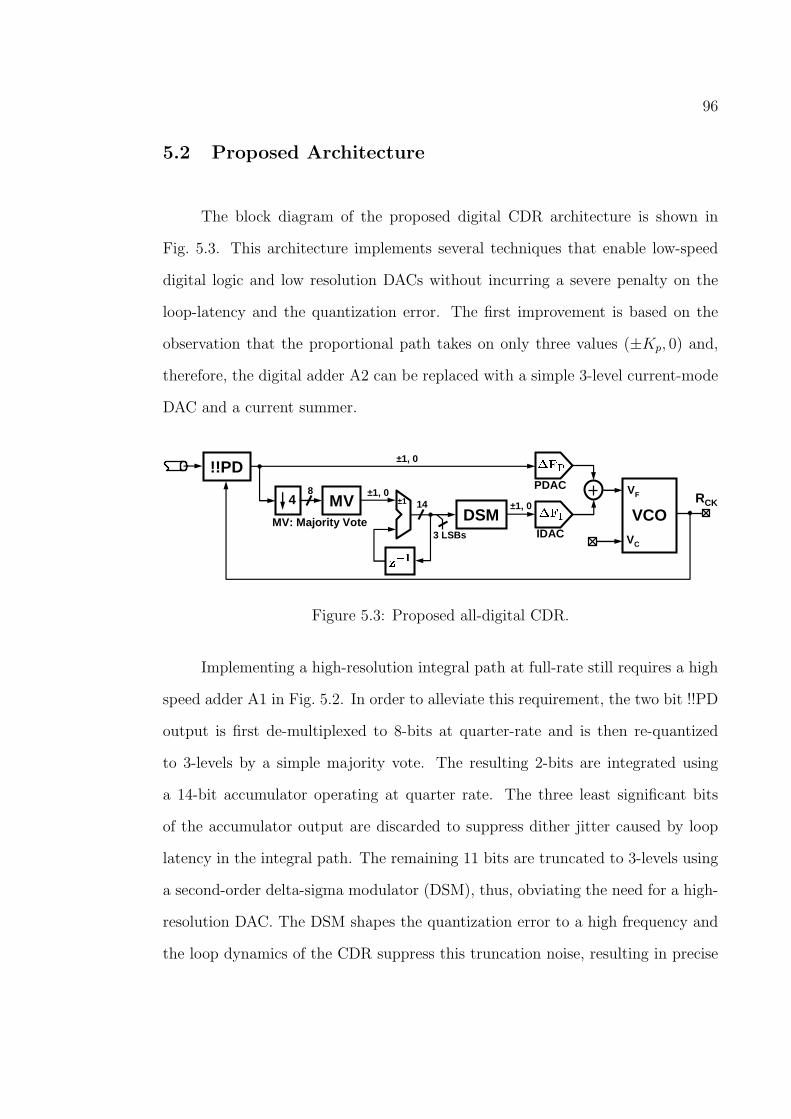
96
5.2 Proposed Architecture
The block diagram of the proposed digital CDR architecture is shown in
Fig. 5.3. This architecture implements several techniques that enable low-speed
digital logic and low resolution DACs without incurring a severe penalty on the
loop-latency and the quantization error. The first improvement is based on the
observation that the proportional path takes on only three values (±Kp, 0) and,
therefore, the digital adder A2 can be replaced with a simple 3-level current-mode
DAC and a current summer.
DSM±1 14MV4
8
3 LSBsMV: Majority Vote
!!PD
±1, 0
±1, 0
RCK
IDAC
PDAC
VCO
VF
VC
±1, 0
Figure 5.3: Proposed all-digital CDR.
Implementing a high-resolution integral path at full-rate still requires a high
speed adder A1 in Fig. 5.2. In order to alleviate this requirement, the two bit !!PD
output is first de-multiplexed to 8-bits at quarter-rate and is then re-quantized
to 3-levels by a simple majority vote. The resulting 2-bits are integrated using
a 14-bit accumulator operating at quarter rate. The three least significant bits
of the accumulator output are discarded to suppress dither jitter caused by loop
latency in the integral path. The remaining 11 bits are truncated to 3-levels using
a second-order delta-sigma modulator (DSM), thus, obviating the need for a high-
resolution DAC. The DSM shapes the quantization error to a high frequency and
the loop dynamics of the CDR suppress this truncation noise, resulting in precise

97
adjustment of the VCO frequency. The phase noise due to the quantization error
that leaks to the output depends on the architecture of DSM and the sampling
frequency. Simulations show that a second-order DSM operating at one quarter
of the operating frequency contributes less than 2.5ps rms jitter to the recovered
clock. The CDR loop is designed to have an over-damped response by ensuring
that the ratio of the phase change from the proportional path to the phase change
from integral path is more than 1000 [44].
When the frequency offset between the incoming data and the local oscillator
is small, the proportional loop drives the PLL towards lock without cycle slipping.
Phase-lock is acquired by dithering the VCO between two frequencies (±∆FP ) [44].
In this design ∆FP is chosen to achieve approximately ±1500ppm of lock-in range.
In the presence of a larger frequency error, the CDR cycle slips and the integral
loop drives the VCO towards the data frequency in discrete steps. As opposed
to an analog CDR, the discrete VCO control degrades the CDR’s immunity to a
long string of consecutive identical digits (CIDs). In this design, the frequency
resolution is better than 7ppm which results in the CDR’s tolerance to more than
72,000 CIDs.
5.3 Linear Analysis
In this section, we present the linearized analysis of the proposed CDR. The
grossly non-linear transfer characteristic of the !!PD mandates non-linear tech-
niques to fully analyze the CDR behavior. However, it has been shown that the
!!PD can be linearized in the presence of recovered clock jitter [43], [45]. The lin-
earized gain KPD of the !!PD in the presence of σj gaussian clock jitter is equal to
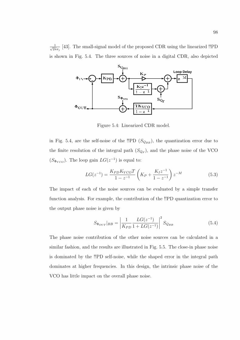
98
1√2πσj
[43]. The small-signal model of the proposed CDR using the linearized !!PD
is shown in Fig. 5.4. The three sources of noise in a digital CDR, also depicted
Loop Delay
Figure 5.4: Linearized CDR model.
in Fig. 5.4, are the self-noise of the !!PD (SQBB), the quantization error due to
the finite resolution of the integral path (SQF), and the phase noise of the VCO
(SΦV CO). The loop gain LG(z−1) is equal to:
LG(z−1) =KPDKV COT
1− z−1
(KP +
KIz−1
1− z−1
)z−M (5.3)
The impact of each of the noise sources can be evaluated by a simple transfer
function analysis. For example, the contribution of the !!PD quantization error to
the output phase noise is given by
SΦOUT|BB =
∣∣∣∣1
KPD
LG(z−1)
1 + LG(z−1)
∣∣∣∣2
SQBB(5.4)
The phase noise contribution of the other noise sources can be calculated in a
similar fashion, and the results are illustrated in Fig. 5.5. The close-in phase noise
is dominated by the !!PD self-noise, while the shaped error in the integral path
dominates at higher frequencies. In this design, the intrinsic phase noise of the
VCO has little impact on the overall phase noise.

99
0.001 0.01 0.1 1 10 200-250
-230
-210
-190
-170
-150
-130
-110
-90
Offset frequency [MHz]
Ou
tpu
t ph
ase
no
ise
[dB
c/H
z]
Figure 5.5: Output phase noise contribution from individual noise sources(σj = 7.5ps, ∆FP = 4MHz, ∆FI = 12MHz, M=3, T = 625ps)
.
5.4 Circuit Design
The proposed CDR is a digital intensive circuit. The digital building blocks
such as adders can be built using simple digital logic or can be synthesized using
standard cells. This section will focus on the design of the analog building blocks
such as the receiver frontend, the 3-level DAC and the 4-stage ring oscillator. The
receiver frontend circuitry shown in Fig. 5.6, recovers data (RDATA) and performs
bang-bang phase detection through early (E) and late (L) signals. Sense amplifiers
are used as data and edge samplers.
The VCO is implemented as a four stage ring oscillator and employs split-
tuned differential cells shown in Fig. 5.7. Pseudo-differential inverters with rail-to-
rail swing are used as the delay elements. The external coarse control voltage (VC)
is used to bring the VCO to within the pull-in range of the CDR. A duty cycle

100
D
QD
Q
D
D
RCK
RDATA
E
L
Figure 5.6: Data recovery and phase detection circuit.
correcting buffer (not shown in Fig. 5.7) maintains accurate duty cycle (50% ±1.5%) under process, temperature and voltage variations. The simulated phase
noise of the VCO (including DACs) oscillating at 1.6GHz is -102dBc/Hz at 3MHz
offset. The external coarse control is used to bring the VCO to within the pull-in
VF
VC
VC
VF
6X
1X
Figure 5.7: 4-stage VCO employing split-tuned delay cell.
range of the CDR. The fine control voltage VF controls all four delay elements to
preserve equal spacing between the phases, thus, making this architecture suitable
for multi-phase clock recovery. The fine control voltage is generated by summing
the proportional (PDAC) and integral (IDAC) paths in the current domain by
3-level DACs as shown in Fig. 5.8. The 3-level input −1, 0, +1 is converted to an
output current (Io) 0, I, and 2I respectively. The transistor M3 is used to minimize

101
glitches due to charge sharing and thereby reduce pattern jitter.
VB2
UPDN
IO
UP
DNIO
IDAC
PDAC
VB1
VF
UP ↔↔↔↔ +1DN ↔↔↔↔ -1
M1
M2
M3
Figure 5.8: DACs to generate fine control voltage VF .
5.5 Experimental Results
A test chip fabricated in a 0.13µm CMOS process occupies 0.1mm2 active
area and operates off of a single-pin 1.2V power supply. The recovered data and
the recovered clock operating at 1.6Gbps are shown in Fig. 5.9. The jitter of the
recovered clock, with 27 − 1 PRBS data is 8.9ps rms (Fig. 5.10) and this jitter
increases to 9.9ps with 231 − 1 PRBS data. The measured bit error rate (BER) is
less than 10−12 with about 50mV of received data amplitude and 600ppm frequency
offset. Fig. 5.11 shows the recovered clock spectrum when the DSM is clocked at
200MHz and 400MHz, respectively. This figure demonstrates, as expected, that
clocking the DSM at lower speed results in a prohibitively large quantization noise
leakage to the output. The measured jitter tolerance is greater than 2UI at a 2MHz
modulation frequency. The coarse tuning range of the VCO is 0.8-1.8GHz. The
chip micrograph is shown in Fig. 5.12 and the CDR performance is summarized in
Table 5.1 .
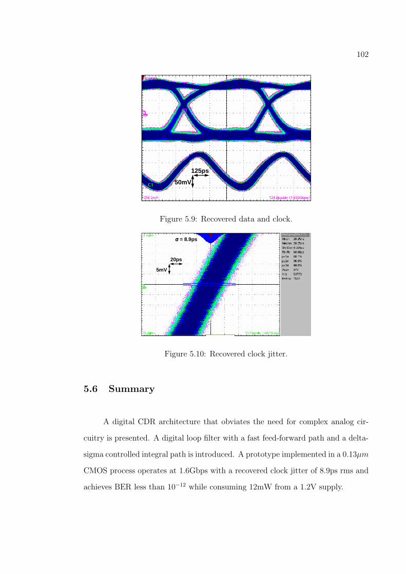
102
50mV
125ps
Figure 5.9: Recovered data and clock.
5mV
20ps
σσσσ = 8.9ps
Figure 5.10: Recovered clock jitter.
5.6 Summary
A digital CDR architecture that obviates the need for complex analog cir-
cuitry is presented. A digital loop filter with a fast feed-forward path and a delta-
sigma controlled integral path is introduced. A prototype implemented in a 0.13µm
CMOS process operates at 1.6Gbps with a recovered clock jitter of 8.9ps rms and
achieves BER less than 10−12 while consuming 12mW from a 1.2V supply.

103
@400MHz@200MHz
Figure 5.11: Recovered clock spectrum. (DSM clocked at 200MHz and 400MHz)
INTEGRAL CONTROLVCO
DACS
ERRORCHECKER
!!PD
Figure 5.12: Chip micrograph.
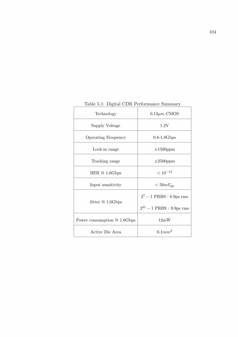
104
Table 5.1: Digital CDR Performance Summary
Technology 0.13µm CMOS
Supply Voltage 1.2V
Operating Frequency 0.8-1.8Gbps
Lock-in range ±1500ppm
Tracking range ±2500ppm
BER @ 1.6Gbps < 10−12
Input sensitivity < 50mVpp
Jitter @ 1.6Gbps27 − 1 PRBS : 8.9ps rms
231 − 1 PRBS : 9.9ps rms
Power consumption @ 1.6Gbps 12mW
Active Die Area 0.1mm2

CHAPTER 6. CONCLUSIONS
The need for high performance digital systems mandates wide-bandwidth
connections between individual ICs in the system. The limitations in the inter-
connect technology and several restrictions imposed by CMOS scaling manifest as
reduced voltage and timing margins in these communication links. These reduced
margins combined with the need for low-power and small-area circuits to perform
high-speed communication between ICs make the design of such links a challenging
design task. This thesis explored design techniques that seek to reduce clock jitter
and hence improve timing margins of the link.
In Chapter 2, a method to analyze the impact of clock jitter on high-speed
links is presented. Based on the linear time-invariant assumptions of the channel
and using the first-order Taylor series approximation, analytical expressions rep-
resenting the detector input for various conditions are derived. Interestingly, this
analysis shows that the transmitter jitter has more deleterious effect on the link
performance compared to receiver jitter.
In Chapter 3, the problem of clocking source synchronous interfaces is ad-
dressed. In particular, design techniques to implement the most important building
block of the data recovery loop namely, a digital to phase converter is presented.
It has been shown that the use of a delta-sigma modulator to shape the phase
noise to high frequencies and then filtering it out by a DLL phase filter presents an
attractive alternative to the design of high resolution digital to phase converters.
In Chapter 4, a hybrid analog/digital clock and data recovery circuit that
achieves a wide tracking range is presented. The wide-operating range analog PLL

106
uses split-tuning and the digital CDR employs a delta-sigma modulator to achieve
precise phase and frequency resolution and a second-order digital loop filter to
achieve wide tracking range.
Finally, in Chapter 5, a digital CDR that obviates the need for a charge pump
and large loop filter is presented. This digital CDR achieves near-analog perfor-
mance with a largely digital circuit. This author believes such digital circuits that
perform traditionally analog functions such as phase-locking offer several benefits
when implemented in deep sub-micron CMOS processes and are therefore worth
researching further.

107
BIBLIOGRAPHY
[1] D. Schmidt, “Circuit pack parameter estimation using Rent’s rule,” IEEETrans. Computer-Aided Design, pp. 186–192, Oct. 1989.
[2] G. Moore, “Cramming more components onto integrated circuits,” Electron-ics, pp. 114–117, Apr. 1965.
[3] W. Dally and J. Poulton, Digital Systems Engineering, Cambridge UniversityPress, Cambridge, UK, 1998.
[4] P. Hanumolu, G. Wei, and U. Moon, “Equalizers for high-speed serial links,”in Design of High-Speed Communication Circuits, R. Harjani, Ed., pp. 175–204. World Scientific Publishing Company, 2006.
[5] B. Casper, M. Haycock, and R. Mooney, “An accurate and efficient analy-sis method for multi-Gb/s chip-to-chip signaling schemes,” in IEEE VLSICircuits Sym. Tech. Papers, June 2002, pp. 54–57.
[6] M. Shinagawa, Y. Akazawa, and T. Wakimoto, “Jitter analysis of high-speedsampling systems,” IEEE J. Solid-State Circuits, vol. 25, pp. 220–224, Feb.1990.
[7] H. Tao, L. Toth, and J. Khoury, “Analysis of timing jitter in bandpass sigma-delta modulators,” IEEE Trans. Circuits Syst. II, vol. 46, pp. 991–1001, Aug.1999.
[8] J. Proakis, Digital Communications, McGraw-Hill Education, 2000.
[9] E. Lee and D. Messerschmitt, Digital Communication, Kluwer AcademicPublishers, 1994.
[10] A. Fiedler, R. Mactaggart, J. Welch, and S. Krishnan, “A 1.0625Gbps trans-ceiver with 2x-oversampling and transmit signal pre-emphasis,” in ISSCCDig. Tech. Papers, Feb. 1997, pp. 238–239.
[11] R. Gu, J. Tran, H. Lin, A. Yee, and M. Izzard, “A 0.5-3.5Gb/s low-powerlow-jitter serial data CMOS transceiver,” in ISSCC Dig. Tech. Papers, Feb.1999, pp. 352–353.
[12] J. Sonntag and R. Leonowich, “A monolithic CMOS 10MHz DPLL for burst-mode data retiming,” in ISSCC Dig. Tech. Papers, Feb. 1990, pp. 194–195.
[13] T. Lee, K. Donnelly, J. Ho, J. Zerbe, M. Johnson, and T. Ishikawa, “A2.5V CMOS delay-locked loop for 18Mbit, 500 megabyte/s DRAM,” IEEEJ. Solid-State Circuits, vol. 29, pp. 1491–1496, Dec. 1994.

108
[14] S. Sidiropoulos and M. Horowitz, “A semidigital dual delay-locked loop,”IEEE J. Solid-State Circuits, vol. 32, pp. 1683–1692, Nov. 1997.
[15] J. Chou, Y. Hsieh, and J. Wu, “A 125MHz 8b digital-to-phase converter,”in ISSCC Dig. Tech. Papers, Feb. 2003, pp. 436–505.
[16] D. Weinlader, Precision CMOS Receivers for VLSI testing applications,Ph.D. thesis, Stanford University, November 2001.
[17] A. Hajimiri, S. Limotyrakis, and T. Lee, “Jitter and phase noise in ringoscillators,” IEEE J. Solid-State Circuits, vol. 34, pp. 790–804, June 1999.
[18] B. Miller and B. Conley, “A multiple modulator fractional divider,” in Proc.of Symp. on Frequency Control, May 1990, pp. 23–25.
[19] P. Hanumolu, V. Kratyuk, G. Wei, and U. Moon, “A sub-picosecond reso-lution 0.5-1.5GHz digital-to-phase converter,” in IEEE VLSI Circuits Sym.Tech. Papers, June 2006, pp. 92–93.
[20] R. Schreier and G. Temes, Understanding Delta-Sigma Data Converters,Wiley-IEEE Press, New Jersey, 2005.
[21] A.Ravi, R. Bishop, L. Carley, and K. Soumyanath, “8 GHz, 20mw, fastlocking, fractional-N frequency synthesizer with optimized 3rd order, 3/5-bitIIR and 3rd order 3-bit-FIR noise shapers in 90nm CMOS,” in Proc. of IEEECICC, Oct. 2004, pp. 625–628.
[22] M. Mansuri, D. Liu, and C. Yang, “Fast frequency acquisition phase-frequency detectors for Gsamples/s phase-locked loops,” IEEE J. Solid-StateCircuits, vol. 37, pp. 138–452, Oct. 2002.
[23] J. Lee and B. Kim, “A low-noise fast-lock phase-locked loop with adaptivebandwidth control,” IEEE J. Solid-State Circuits, vol. 35, pp. 1137–1145,Aug. 2000.
[24] P. Hanumolu, M. Brownlee, K. Mayaram, and U. Moon, “Analysis of charge-pump phase-locked loops,” IEEE Trans. Circuits Syst. I, vol. 51, pp. 1665–1674, Sept. 2004.
[25] J. Yuan and C. Svensson, “High speed CMOS circuit technique,” IEEE J.Solid-State Circuits, vol. 24, pp. 62–70, Feb. 1989.
[26] S. Sidiropoulos, C. Yang, and M. Horowitz, “A CMOS 500Mbps synchronouspoint to point link,” in Proc. IEEE Symp. VLSI Circuits, June 1994, pp.43–44.
109
[27] S. Sidiropoulos, D. Liu, J. Kim, G. Wei, and M. Horowitz, “Adaptive band-width DLLs and PLLs using regulated supply CMOS buffers,” in Proc. IEEESymp. VLSI Circuits, June 2000, pp. 124–127.
[28] P. Raha, “A 0.6-4.2V low-power configurable PLL architecture for 6GHz-300MHz applications in a 90nm CMOS process,” in IEEE VLSI CircuitsSym. Tech. Papers, June 2004, pp. 232–235.
[29] B. Razavi, Y. Ota, and R. Swartz, “Design techniques for low-voltage high-speed digital bipolar circuits,” IEEE J. Solid-State Circuits, vol. 29, pp.332–339, Mar. 1994.
[30] P. Larsson, “A 2-1600-MHz CMOS clock recovery pll with low-vdd capabil-ity,” IEEE J. Solid-State Circuits, vol. 34, pp. 1951–1960, Dec. 1999.
[31] P. Hanumolu, G. Wei, and U. Moon, “A wide tracking range 0.2–4Gbpsclock and data recovery circuit,” in IEEE VLSI Circuits Sym. Tech. Papers,June 2006, pp. 88–89.
[32] R. Walker, “Designing bang-bang PLLs for clock and data recovery in serialdata transmission systems,” in Phase-Locking in High-Performance Systems:From Devices to Architectures, B. Razavi, Ed., pp. 34–45. Wiley-IEEE Press,2003.
[33] S. Williams, H. Thompson, M. Hufford, and E. Naviasky, “An improvedCMOS ring oscillator pll with less than 4ps RMS accumulated jitter,” inProc. of IEEE CICC, Oct. 2004, pp. 151–154.
[34] B. Lee, M. Hwang, S. Lee, and D. Jeong, “A 2.5-10-Gb/s CMOS trans-ceiver with alternating edge-sampling phase detection for loop characteristicstabilization,” IEEE J. Solid-State Circuits, vol. 38, pp. 1821–1829, Nov.2003.
[35] M. Matsui et al., “A 200 MHz 13 mm2 2-D DCT macrocell using sense-amplifying pipeline flip-flop scheme,” IEEE J. Solid-State Circuits, vol. 29,pp. 1482–1490, Dec. 1994.
[36] B. Nikolic et al., “Improved sense-amplifier-based flip-flop: design and mea-surements,” IEEE J. Solid-State Circuits, vol. 35, pp. 876–884, June 2000.
[37] J. Alexander, “Clock recovery from random binary signals,” Electr. Lett.,pp. 541–542, Oct. 1975.
[38] J. Craninckx and M. Steyaert, “A 1.75-GHz/3-V dual-modulus divide-by-128/129 prescaler in 0.7-µm CMOS,” IEEE J. Solid-State Circuits, vol. 31,pp. 890–897, July 1996.
110
[39] M. Perrott, Techniques for high data rate modulation and low power operationof fractional-N frequency synthesizers, Ph.D. thesis, Massachusetts Instituteof Technology, 1997.
[40] N. Krishnapura and P. Kinget, “A 5.3-GHz programmable divider for Hiper-LAN in 0.25-µm CMOS,” IEEE J. Solid-State Circuits, vol. 35, pp. 1019–1024, July 2000.
[41] J. Cao et al., “OC-192 transmitter and receiver in standard 0.18µm CMOS,”IEEE J. Solid-State Circuits, vol. 37, pp. 1768–1780, Dec. 2002.
[42] S. Anand and B. Razavi, “A 2.75Gb/s CMOS clock recovery circuit withbroad capture range,” in ISSCC Dig. Tech. Papers, Feb. 2001, pp. 214–215.
[43] J. Sonntag and J. Stonick, “A digital clock and data recovery architecturefor multi-gigabit/s binary links,” in Proc. of IEEE CICC, Sept. 2005, pp.532–539.
[44] R. Walker, C. Stout, J. Wu, B. Lai, C. Yen, T. Hornak, and P. Petruno,“Two-chip 1.5-GBd serial link interface,” IEEE J. Solid-State Circuits, vol.27, pp. 1806–1811, Dec. 1992.
[45] J. Lee, K. Kundert, and B. Razavi, “Analysis and modeling of bang-bangclock and data recovery circuits,” IEEE J. Solid-State Circuits, vol. 39, pp.1571–1580, Sept. 2004.