Embed Size (px)
Citation preview

Copyright
by
Manish Kumar Niranjan
2007

The Dissertation Committee for Manish Kumar Niranjancertifies that this is the approved version of the following dissertation:
THEORETICAL INVESTIGATION OF CONTACT MATERIALS FOR
EMERGING ELECTRONIC AND SPINTRONIC DEVICES
Committee:
_______________________________
L. Kleinman, Co-Supervisor
_______________________________
A. A. Demkov, Co-Supervisor
_______________________________
A. H. MacDonald
_______________________________
M. Tsoi
_______________________________
S. K. Banerjee
_______________________________
J. Chelikowsky

THEORETICAL INVESTIGATION OF CONTACT MATERIALS FOR
EMERGING ELECTRONIC AND SPINTRONIC DEVICES
by
Manish Kumar Niranjan, M.S
Dissertation
Presented to the Faculty of the Graduate School of
The University of Texas at Austin
In Partial Fulfillment
of the Requirements
for the Degree of
Doctor of Philosophy
The University of Texas at Austin
December 2007

iv
Acknowledgement
I would like to express my deep and sincere gratitude to my supervisors, Professor
Leonard Kleinman and Professor Alexander A. Demkov, for their guidance,
encouragement and support during the entire period of PhD work.
I warmly thank Dr. B. R. Sahu for his personal guidance and suggestions on many
topics.
I warmly thank Dr. Stefan Zollner for introducing and encouraging me to work on
contact materials significant to semiconductor industry.
My warm thanks are due to Dr. S. C. Song, Dr. Prashant Majhi and Dr. H.
Mustafa for their supervision during the internship period at SEMATECH Inc.
My sincere thanks are due to all committee members Prof. A. H. MacDonald,
Prof. S. Banerjee, Prof. M. Tsoi and Prof. J. Chelikowsky.
Finally, I would like to thank my friends Adrian Ciucivara and Dr. M. N. Huda
who always kept the atmosphere cheerful with their warm presence.
MANISH KUMAR NIRANJAN
The University of Texas at Austin
August 2007

v
THEORETICAL INVESTIGATION OF CONTACT MATERIALS FOR
EMERGING ELECTRONIC AND SPINTRONIC DEVICES
Publication No. _____________
Manish Kumar Niranjan, Ph.D.The University of Texas at Austin, 2007
Supervisors: Leonard Kleinman and Alexdander A. Demkov
We present a theoretical study of the electronic structure, surface energies and
work functions of orthorhombic Pt monosilicide and germanides of Pt, Ni, Y and Hf
within the framework of density functional theory (DFT). Calculated work functions for
the (001) surfaces of PtSi, NiGe and PtGe suggest that these metals and their alloys can
be used as self-aligned contacts to p-type silicon and germanium. In addition, we also
study electronic structure and calculate the Schottky-barrier height at Si(001)/PtSi(001) interface
and GaAs(001)/NiPtGe(001) interfaces with different GaAs(001) and NiPtGe (001) terminations.
The p-type Schottky barrier height of 0.28 eV at Si/PtSi interface is found in good
agreement with predictions of a simple metal induced gap states (MIGS) theory and
available experiment. This low barrier suggests PtSi as a low contact resistance junction
metal for silicon CMOS technology. We identify the growth conditions necessary to
stabilize this orientation. The calculated p-type Schottky barrier heights (SBH) at different
GaAs/NiPtGe interfaces vary by as much as 0.18 eV around the average value of 0.5 eV. We
further identify and discuss factors responsible for strong Fermi level pinning resulting in small
variation in the p-SBH. We also present a theoretical study of magnetic state of β-MaAs and
show that it is antiferromagnetic and explain the lack of observed long-range order.
vi
Contents
Acknowledgements iv
Abstract v
List of Figures ix
List of Tables xiii
Chapter 1 Introduction 1
1.1 CMOS transistor and use of silicides (germanides) ……………… 2
1.2 Metal-Semiconductor contact ……………………………………. 8
1.2.1 Current transport mechanism through metal-semiconductor
(M/S) interface ……………………………………………… 9
1.2.2 Experimental techniques to probe metal/semiconductor-
-interfaces ………………………………………………… 11
1.3 SBH, Fermi level pinning and phenomenological models ……… 13
1.3.1 Theory of SBH in presence of surface states ……………… 18
1.3.2 MIGS, Defect states and Disorder induced gap state-
-models ……………………………………………………. 21
1.3.3 Limitations of the MIGS model …………………………… 25
1.3.4 Theory of SBH based on the interfacial chemical-
-bonding …………………………………………………… 26
Chapter 2 Methodology 30
2.1 Ab-initio calculations …………………………………………..... 30
2.1.1 Fundamental equations for interacting electrons-
-and nuclei ………………………………………………….. 31
2.1.2 Born-Oppenheimer or adiabatic approximation …………... 32

vii
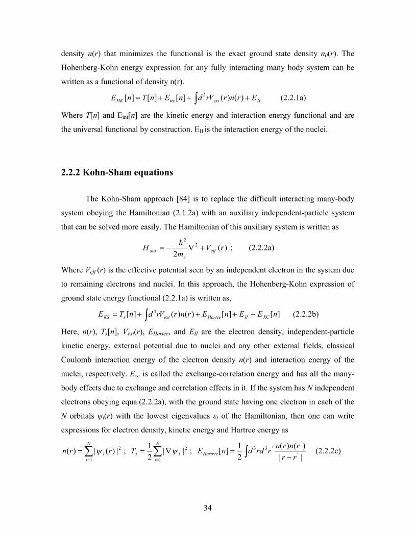
2.2 Density functional theory ……………………………………….. 33
2.2.1 Hohenberg-Kohn theorems ………………………………. 33
2.2.2 Kohn-Sham equations …………………………………… 34
2.2.3 Local density approximation (LDA) …………………….. 37
2.2.4 Generalized-gradient approximation (GGA) ……………. 37
2.2.5 Discussion ………………………………………………… 38
2.3 Application to atomic systems (bulk, surfaces, interfaces etc.)….. 38
2.3.1 Plane Wave expansion ……………………………………. 39
2.3.2 Pseudopotential approximation …………………………… 40
2.3.3 Projector augmented wave (PAW) method ……………...... 43
2.3.4 Brillouin zone integration …………………………………. 44
2.3.5 Supercell technique ……………………………………...... 45
2.3.6 Band structure alignment and Schottky barriers ………. … 46
2.3.7 Thermodynamics of surfaces and calculation of-
-surface energies ………………………………………….. 53
2.3.8 Elastic Constants ………………………………………….. 56
Chapter 3 Electronic structure, surface energies and work-
-functions of PtSi 60
3.1 Crystal and electronic structure of bulk PtSi ………………………... 61
3.2 Surface energies of different PtSi surface orientations ……………… 66
3.3 Work function at different PtSi surface orientations ………………… 72
3.4 Schottky Barrier height at the Si(001)/PtSi(001) interface ………….. 74
3.5 Conclusion ………………………………………………………….... 80

viii
Chapter 4 Electronic structure, surface energies and work-
-functions of NiGe and PtGe 81
4.1 Crystal and electronic structure of bulk NiGe and PtGe …………….. 82
4.2 Elastic constants ……………………………………………………... 90
4.3 Surface energy and reconstruction of NiGe and PtGe ……………….. 94
4.4 Work function at different NiGe and PtGe surfaces …………………. 105
4.5 Conclusion ………………………………………………………. ….. 107
Chapter 5 Electronic structure and Schottky-barrier height-
-at GaAs(001)/Ni0.5Pt0.5Ge(001) interface 108
5.1 Interface structure …………………………………………………..... 109
5.2 Schottky barrier height at the GaAs/NiPtGe interface ………………. 113
5.3 Electronic structure of GaAs(001)/Ni0.5Pt0.5Ge interface …………...... 116
5.4 Conclusion…………………………………………………………… 118
Chapter 6 Magnetic state of β-MnAs 125
6.1 Calculations and Results …………………………………………..... 127
6.2 Conclusion …………………………………………………….......... 134
References 136
Vita 146

ix
List of Figures
1.1a Cross section of modern CMOS transistors with an n-channel
MOSFET (n-MOSFET) and a p-channel MOSFET (p-MOSFET) ……….... 3
1.1b Maximum contact resistivity as predicted in ITRS 1999 and 2002 update … 4
1.1c Scaling of sheet resistance as predicted in ITRS (1999 and 2002 update)….. 4
1.1d Evolution of gate sheet resistance with gate technology over time…………. 6
1.1e Resistance components for the series resistance from the source/drain
region to the channel……………………………………………………….. 7
1.3a Schematic band diagram of band bending according to the Schottky
model for the MS interface………………………………………………… 15
1.3b Barrier height at metal/GaAs as a function of metal work function............. 16
1.3c Barrier height at metal/n-Si as a function of metal work function………… 16
1.3d Schematic band diagram of band bending according to the Bardeen
model for the MS interface………………………………………………… 17
1.3.1a Energy band diagram of a metal- n-type semiconductor contact
with an interfacial layer…………………………………………………… 18
1.3.2a An energy E of a surface state in the band gap of the semiconductor
corresponds to two propagating Bloch functions k1, -k1 in the metal……... 22
1.3.2b Slope parameter S plotted versus the electronic contribution ε∞ of
the dielectric constant of the semiconductor……………………………… 23
1.3.4a Experimentally observed slope parameters S are used to plot the
quantity [ε∞(1-S)]-1 against the semiconductor band gap…………………. 29
2.2.2a Flowchart of self-consistent Kohn-Sham calculation…………………….. 36
2.3.6a Schematic illustration of the band structure lineup problem
between semiconductors A and B………………………………………… 47
3.1a The orthorhombic unit cell of bulk PtSi…………………………………... 61
3.1b Band energies at the high symmetry k-points in the Brillouin zone

x
for bulk PtSi………………………………………………………………. 63
3.1c The density of states of PtSi (in electrons per Å3 per eV)……………….. 64
3.1d The density of states in PtSi (in electrons per Å3 per eV) site
projected on Pt atoms……………………………………………………. 64
3.1e Projected density of states (in electrons per Å3 per eV) of Si in PtSi……. 65
3.1f Density of states (in electrons per Å3 per eV) of bulk Pt………………… 65
3.1g The density of states in Pt projected onto Pt sites……………………….. 66
3.2a The Simulation cell for the (001)-oriented PtSi surface slab……………. 67
3.2b PtSi (001) surface (side view). Top four layers are shown……………… 68
3.2c Top view of the first plane of PtSi (001) surface. Displacements
of the atoms after the relaxation are indicated by the arrows………....... 69
3.2d Surface energies of PtSi surfaces as the function of Pt chemical
Potential………………………………………………………………… 71
3.3a The planar averaged coulomb potential and work function of
the PtSi (001) surface. Z is the direction normal to the (001) surface…… 74
3.4a A schematic of the band alignment at the Si(001)-PtSi(001) interface….. 76
3.4b The Si(001)/PtSi(001) interface structure……………………………….. 78
3.4c The average coulomb potential (in eV) of Si and PtSi in Si(001)/PtSi(001)
supercell along Z (slab axis)…………………………………………….. 79
3.4d The density of states (in electrons Å3 per eV) site projected on a Si
atom deep inside the Si side of Si(001)/PtSi(001) interface…………….. 80
4.1a The orthorhombic unit cell of bulk NiGe and PtGe……………………… 82
4.1b Energy Bands of bulk NiGe………………………………………………. 85
4.1c Energy Bands of bulk PtGe……………………………………………….. 86
4.1d The total density of states of NiGe (in electrons per Å3 per eV)………….. 86
4.1e The partial density of states of NiGe (in electrons per Å3 per eV)
projected onto Ni atoms…………………………………………………… 87
4.1f The partial density of states of NiGe (in electrons per Å3 per eV)
projected onto Ge atoms…………………………………………………… 87
4.1g The total density of states of PtGe (in electrons per Å3 per eV)……………. 88
xi
4.1h The partial density of states of PtGe (in electrons per Å3 per eV)
projected onto Pt atoms……………………………………………………. 88
4.1i The partial density of states of PtGe (in electrons per Å3 per eV)
projected onto Ge atoms…………………………………………………… 89
4.1j Valance electron charge density (electrons/Å3) contours in
the (001) plane for NiGe unit cell…………………………………………. 89
4.1k Valance electron charge density (electrons/Å3) contours in
the (001) plane for Ni unit cell……………………………………………. 90
4.3a Top view of the unreconstructed NiGe (001) surface……………………… 95
4.3b NiGe (001) surface (side view)…………………………………………….. 95
4.3c Side view of the unreconstructed Ge-terminated NiGe (101) surface……… 97
4.3d Side view of the reconstructed Ge-terminated NiGe (101) surface………… 98
4.3e Top view of the unreconstructed Ge-terminated NiGe (101) surface………. 99
4.3f Top view of the reconstructed Ge-terminated NiGe (101) surface…………. 99
4.3g Valance electron charge density (electrons/Å3) contours
at NiGe(101)-1x1 (Ge terminated) reconstructed surface………………….. 100
4.3h Surface energies of NiGe surfaces as a function of Ni chemical potential…. 103
4.3i Surface energies of PtGe surfaces as a function of Pt chemical potential….. 105
4.4a The planar averaged coulomb potential and work function of the
NiGe (001) surface…………………………………………………………. 107
5.1a Top view of GaAs (001) and NiPtGe (001) surfaces and surface unit cells… 112
5.1b (Left) Side view of GaAs (001)/NiPtGe(001) interface with
As-terminated GaAs(001) and NiGe terminated NiPtGe (001) surface.
(Right) Side view of GaAs (001)/NiPtGe (001) interface
with Ge vacancies…………………………………………………………. . 112
5.2a The average coulomb potential (in eV) in GaAs(001)/NiPtGe(001)
supercell along Z (growth axis)……………………………………………. 116
5.3a Density of states projected on p-orbitals of As and Ge atoms, d-orbital
of Ni atom located in different layers from the NiPtGe/GaAs
interface in the supercell (GaAs(001) is As-terminated and

xii
NiPtGe is NiGe terminated). Topmost DOS denotes nearest
while bottom-most denotes farthest from the interface…………………... 119
5.3b Two dimensional band structure for GaAs/NiPtGe interface (GaAs(001)
is As-terminated and NiPtGe is NiGe terminated)……………………… 120
5.3c GaAs/NiPtGe interface bands (light lines) around the Fermi
level (dashed line)……………………………………………………… 121
5.3d Charge density along the slab axis for the band (shown in Figure 5.3b)
between 0 to 1 eV……………………………………………………… 122
5.3e Charge density along the slab axis for the band (shown in Figure 5.3b)
around 8 eV……………………………………………………………. 122
5.3f Density of states projected on p-orbitals of Ga and Ge atoms, d-orbital
of Ni atom located in different layers from the NiPtGe/GaAs interface
in the supercell…………………………………………………………. 123
5.3g Density of states projected on p-orbitals of As and Ge atoms, d-orbital
of Pt atom located in different layers from the NiPtGe/GaAs interface
in the supercell………………………………………………………… 124
6a (a) α-MnAs (B81) unit cell containing two Mn and two As atoms, (b)
β-MnAs (B31) unit cell containing four Mn and four As atoms………. 127
6.1a Magnetization of a-MnAs in bohr magnetons per MnAs (solid line)
and negative of the cohesive energy per MnAs in eV (dashed line) as a
function of volume……………………………………………………… 128
6.1b Majority (solid line) and minority spin (dashed line) densities of states
in electrons per eV per unit cell of α-MnAs………..……………………. 130
6.1c Antiferromagnetic models of β-MnAs used for calculations……………. 132
6.1d Total density of states in electrons per eV per unit cell of β-MnAs. The
Fermi energy is at E=0…………………………………………………… 132

xiii
List of Tables
1.2.2a Electronic and optical techniques for characterizing semiconductor surfaces
and interfaces and the corresponding information they can provide………. 13
2.3.8a Parameterizations of the three strains used to calculate the three elastic
constants of cubic Ni and Ge………………………………………………. 58
2.3.8b Parameterizations of the nine strains used to calculate the nine elastic
constants of orthorhombic NiGe…………………………………………… 59
3.1a Theoretical and experimental lattice constants (in Å); heat of formations
(in eV/atom); cohesive energy (in eV/atom)………………………………. 62
3.1b Experimental and calculated free internal in plane coordinates of PtSi…… 62
3.2a Surface rumpling in % for PtSi (001) surface……………………………… 68
3.2b Surface energies (in erg/cm2) and Work functions (in eV) for
different PtSi surface orientations………………………………………… 72
4.1a Theoretical and experimental lattice constants, heat of formations, and
cohesive energy for Ni, Pt, NiGe, PtGe and Ge…………………………… 83
4.1b Experimental and calculated free internal in-plane coordinates of NiGe
and PtGe…………………………………………………………………… 83
4.2a Calculated and experimental elastic constants (in the units of GPa) of
Ge, Si, Ni and Pt………………………………………………………….. 93
4.2b Calculated elastic constants and bulk modulus (in units of GPa) of
NiGe, and PtGe…………………………………………………………… 93
4.3a Surface rumpling and inter-planar relaxation in % for the NiGe (001)
surface……………………………………………………………………. 96
4.3b Surface rumpling and inter-planar relaxation in % for the NiGe (101)
surface……………………………………………………………………. 100

xiv
4.3c Surface energies and work functions for different NiGe surface
orientations………………………………………………………………. 102
4.3d Surface energies and work functions for different PtGe surface
orientations………………………………………………………………. 104
5.1a Theoretical and experimental lattice constants and internal in-plane
coordinates of NiGe, PtGe and Ni0.5Pt0.5Ge………………………………. 110
5.2a Calculated p-Schottky barrier height at the GaAs/NiPtGe interface with
different GaAs(001) and NiPtGe(001) termination……………………….. 115
6.1a Equilibrium unit-cell volume (in bohr3), cohesive energy (in eV per MnAs),
c/a ratio, magnetization (in bohr magnetons per Mn atom), and bulk modulus
(in GPa) compared with experiment for α-MnAs………………………… 129
6.1b Cohesive energy (per MnAs) calculated at the experimental
high-temperature lattice constants and inner displacements as well as
with lattice constants and inner displacements relaxed to their
equilibrium values for ferromagnetic, paramagnetic, and
three antiferromagnetic structures (Fig 6.1c) described in text……………. 131
6.1c Calculated orthorhombic lattice constants (in bohr), volume (in bohr3),
and magnetization (in bohr magnetons per MnAs) for the five crystals in
Table 6.1b, compared with experimental values at 55 °C and 4.2 K with
an applied pressure of 12.6 kbar…………………………………………. 133
6.1d Calculated positions of the atoms within the unit cells of Table 6.1c
compared with experiment at 55 °C….…………………………………. 134

1
Chapter 1
Introduction
The rapid advancement in microelectronics during the last 40 years has been
realized through miniaturization and integration of the electronic devices into integrated
circuits (IC) based on complementary metal oxide semiconductor (CMOS) technology.
CMOS technology uses n-type and p-type field effect transistors (FETs) to produce
digital logic elements that are superior to other available logic technologies for many
applications. The dominance of CMOS over technologies is based on its low power
consumption as well as the ability to scale CMOS and achieve simultaneous
improvements in power consumption, speed and cost. As the result of continuous device
scaling (miniaturization of the device), the CMOS transistor dimensions and critical
parameters, such as channel length, oxide layer thickness, etc. have already reached in
nanometers and their further scaling turned out to be challenging. According to the
International Technology Roadmap for Semiconductors (ITRS) [24] one of the most
pressing concerns of CMOS technology beyond the 65 nm node (channel length) is the
contact resistances in source/drain regions between the doped silicon and metal alloy
(silicide). Thus the roadmap calls for a new contact technology by the 45 nm node.
Recently, silicides of platinum and rare earth metals have been found promising to
address contact resistance issue in CMOS.
Furthermore, due to continuous device scaling, silicon CMOS technology is
rapidly reaching fundamental limits and has led to intense research into alternative
channel materials. The low mobility of carriers in silicon is a serious obstacle towards
the performance requirement of nanoscale CMOS transistors as defined in ITRS [24].
Recently, III-V compound semiconductors (such as GaAs, InSb) and germanium have
generated lot of interest as potential candidates for implementation in future CMOS-type
devices, due to their much higher electron mobility than that in silicon [13-18, 25-27].
However, to fully exploit transport properties of germanium, GaAs and other compound

2
semiconductors, a low resistance contact technology will have to be developed, much in
the same way as that in silicon CMOS technology based on metal-silicides. Metal
germanides have attracted much attention recently and seem to be very promising to
make low resistance contacts since they are closely related to analogous silicides in
respect to their compositions and structures.
In this work we study 1) electronic structure, surface energies, work functions of
PtSi, NiGe, PtGe, Y5Ge3, YGe, Hf5Ge3, HfGe 2) electronic structure and SBH at PtSi/Si
and GaAs/NiPtGe interfaces.
The rest of the chapter is organized as follows. In section 1.1, we provide an
overview of CMOS transistor and the role of silicide (germanide) in the formation of low
resistance contacts to source, grain and gate in it. In section 1.2 and 1.3, we discuss metal
semiconductor contacts (M/S) and various models to calculate barrier height at the M/S
interface. And, in section 1.4, we provide an overview of this work/thesis.
1.1 CMOS transistor and use of silicides (germanides)
It is known that metal-oxide-semiconductor field-effect-transistor (MOSFET) is
the basic building block for the absolute majority of today’s electronic systems [29]. A
cross section of two modern MOSFETs placed side-by-side resulting into a CMOS-FET
is shown schematically in Figure 1.1a, with a metal silicide layer present in the three
electrode terminals, gate, source, and drain for both transistors.

3
Figure 1.1a: Cross section of modern CMOS transistors with an n-channel MOSFET (n-
MOSFET) and a p-channel MOSFET (pMOSFET).
The silicide layer is usually formed simultaneously in all six electrode areas. The two
transistors are of opposite polarity, one n-channel MOSFET (n-MOSFET) built directly
on the p-type substrate and one p-channel MOSFET (p-MOSFET) built inside the n-well,
that is, in turn first formed on the same p-type substrate as shown. Constructed
simultaneously on the same substrate, the two transistors are usually connected in series
between the power supply terminals in an electronic circuit to minimize standby power
dissipation, that is, the complementary MOS (CMOS) technology. Among many
technical parameters, the gate length of a MOSFET, which is one of the most critical
indicators of the integration technology, will decrease below 10 nm by year 2016, in
order to attain the desired technological gain and economical profit. Figure 1.1b shows,
how the electrical contact resistivity should be scaled according to ITRS in order to
deliver MOSFETs with the desired performance. Depicted in Figure 1.1c is the ITRS
prediction for how sheet resistance in the source/drain regions of a MOSFET should
scale. The requirements for a decreasing source/ drain series resistance and contact
resistivity in smaller MOSFETs are well treated by Ng and Lynch [30].

4
Figure 1.1b: Maximum contact resistivity as predicted in ITRS 1999 and 2002 update.
Figure 1.1c: Scaling of sheet resistance as predicted in ITRS (1999 and 2002 update).

5
The main driver for the continuous advancement in very large scale integration
(VLSI) has been the search for electronic circuits of higher performance and lower cost.
In particular, the speed of an electronic circuit is one of the major concerns. To enhance
the speed, parasitic capacitance and series resistance should both be minimized to reduce
the RC (resistance-capacitance) time delay and increase the clock frequency [31]. For
this purpose of reaching higher speed, metal silicides have been utilized to form ohmic
contacts with source, drain, and gate silicon because of their low resistivity, low contact
resistance to Si, reasonable thermal stability, and excellent process compatibility with
standard Si technology. Undoubtedly, they have played a crucial part in the rapid
development of microelectronic devices [1], and have recently attracted renewed
attention [2, 3]. Over the past two decades, silicides of Ti, Co and Ni have been
successively used in integrated circuit manufacturing [1-7]. Fig. 1.1d shows evolution of
gate sheet resistance with the use of silicides and reduction of channel length with time.
In the deep submicron regime NiSi is now succeeding CoSi2 [8, 9, 12, 13]. However,
both CoSi2 and NiSi exhibit large (0.5-0.6 eV) Schottky barriers to Si, in addition, NiSi
suffers from low thermal stability [8]. This contact resistance already amounts to a
quarter of the total parasitic resistance [8], and will clearly only rise as scaling continues.
(Fig 1.1e shows all the resistances which can be significant in a MOSFET). Thus, it is
desirable to identify new metals or alloys with a lower Schottky barrier to n- and p- type
Si for use in NMOS and PMOS, respectively [4]. Adding Pt to NiSi significantly
enhances the NiSi thermal stability [10]. PtSi is attractive in its own right as a p-type
contact. It has relatively low (0.2 eV) Schottky barrier on Si (001) and has excellent
thermal stability.

6
Figure 1.1d: Evolution of gate sheet resistance with gate technology over time. Ref [1]
Silicides can be formed by either a solid state reaction between a metal and Si, or by co-
depositing the metal and Si. The solid-state reaction method is used in a salicide process
[1] (self-aligned silicide process), whereas the co-deposition method is used in a polycide
process [1]. Fig. 1.1e shows the parasitic resistances in a MOSFET which can be
significantly large if silicides are not used to form contacts.

7
Figure 1.1e: Resistance components for the series resistance from the source/drain
region to the channel [30].
Unlike metal silicides [1], metal germanides have not, until recently, attracted
much attention, presumably, due to the lack of practical applications. However, this is
about to change, as scaling of traditional silicon based technology is rapidly reaches its
physical limit, a germanium channel field effect transistor (FET) is generating a lot of
interest [13-18]. It is worth noting that the first (bipolar) transistor of Bardeen, Brattain
and Shockley was made of Ge [19]. The germanium channel metal oxide semiconductor
FET (MOSFET) offers high mobility of both carriers (electrons and holes) resulting in
higher overdrive current, enhanced transconductance, and higher cutoff frequencies as
compared with a Si transistor. Historically, the use of germanium has been limited due to
the lack of a stable native oxide and processing technology. Ironically, the emerging use
of alternative high-k dielectrics as the gate insulator in Si-based technology [20] may
help finally realize the full potential of a germanium MOSFET [17, 18]. Nevertheless, to
fully exploit transport properties of germanium, a low resistance contact technology will

8
have to be developed based on metal germanides, much in the same way that self aligned
metal silicides are used in a standard complimentary metal oxide semiconductor (CMOS)
process today. Thus germanides with low n- and p-type Schottky barriers to the
germanium channel (for use in NMOS and PMOS devices) need to be identified.
Germanides are closely related to analogous silicides in respect to their compositions and
structures. In the deep submicron regime (22 nm and below) NiGe, PtGe and their alloys
appear to be promising as low barrier contacts to p-type germanium [21-23].
In addition to germanium, III-V compound semiconductors such as GaAs and
InSb have emerged as potential candidates for implementation in future CMOS-type
devices, due to their much higher electron mobility than that in silicon [25-27].
Compound semiconductors are also attractive materials for applications where silicon can
not be used, such as optoelectronics, high-power devices, high frequency devices, and
high temperature devices. However, transport properties of GaAs and other compound
semiconductors can not be exploited fully with out the development of ohmic contact
technology. Interestingly, germanides of nickel have been used to make contacts in GaAs
based devices [28]. However, their further development is required to address the contact
resistance issues in nanoscale devices.
1.2 Metal-Semiconductor contacts
Metallic contacts to semiconductors are an essential part of most modern
electronic and optoelectronic devices. The electronic structure of metal/semiconductor
(MS) interfaces plays a fundamental role in the transport properties of these junctions.
One of the most relevant parameters of MS junctions is its Schottky barrier height (SBH),
which is a measure of the energy mismatch across the interface between the Fermi energy
of the metal and the majority carrier band edge of the semiconductor. For ohmic contacts,
a vanishing SBH is desirable while larger value of the SBH is sought for more rectifying
contact. However, a control of the SBH is always sought regardless of the application.
Generally, in most cases an ohmic contact is wanted. Due to their technological
importance, MS contacts and their SBH have been the subject of numerous investigations

9
[32, 33]. Despite the enormous progress in solid state physics and semiconductor device
physics, in particular, the factors controlling the SBH are still not yet fully understood.
Recent advances in Schottky barrier concepts have shown the importance of the
occurrence of interfaces states and polarization of the bonds at the interface.
1.2.1 Current transport mechanism, contact resistance and SBH at
metal-semiconductor (MS) interface
When a metal directly contacts a semiconductor, the valence and conduction
bands of the semiconductor bend to make the Fermi levels in the metal and the
semiconductor equal. The carrier transport mechanisms through this M/S interface are
strongly influenced by the doping concentration in the semiconductor (ND), barrier height
(φB) and the temperature (T). When the semiconductor is lightly doped (ND < 1017 cm-3 ),
the depletion width becomes very wide and the electrons cannot tunnel through the
semiconductor interface. The only way the electrons can transport between the
semiconductor and the metal is by thermionic emission (TE) over the potential barrier φB.
In case of medium doping of the semiconductor (1017 < ND < 1018 cm-3), electrons can
partially tunnel through the semiconductor interface and both the thermionic and
tunneling processes are equally important. The current flow is controlled by electrons
with some thermal energy tunneling through the mid-section of the potential barrier. This
is called thermionic field-emission (TFE). When the semiconductor is extremely heavily
doped (>1018 cm– 3), the electrons can tunnel through from the Fermi level in the metal
into the semiconductor. This process is called field-emission (FE).
A useful parameter indicative of the electron tunneling probability is kT/E00,
where E00 is defined by,
*00 4 m
NqhE D
where q is the electronic charge, h is Plancks constant, m* is the effective mass of the
tunneling electron, ε is the dielectric constant of the semiconductor. With increasing the
doping concentration (ND), the width of the depletion region decreases, making it easier

10
for carriers to tunnel through. This indicates that when E00 is high relative to thermal
energy kT, the probability of the electron transport by tunneling increases. Therefore, the
ratio kT/E00 is a useful measure of the relative importance of the thermionic process to the
tunneling process. For lightly doped semiconductors, kT/E00 >> 1 and the thermionic
emission is the dominant current flow mechanism. For kT/E00 ~ 1 both the thermionic and
tunneling mechanisms are dominant, and for kT/E00 << 1, the tunneling mechanism
dominates the current flow. Again, note that the doping level in the semiconductor and
the temperature influence the carrier transport mechanism
The specific contact resistance ρc is given by the reciprocal of the derivative of
the current density with respect to the voltage,
1
0
Vc dV
dJ
The current-voltage relations have been developed based on the simple energy band
models using the Wentzel-Kramers-Brillouin (WKB) approximation [34, 35]. This
approximation provides relatively simple results that are sufficient here to obtain the
basic background for estimating the Ohmic contact resistance ρc.
For the thermionic-emission mechanism, ρc is given by,
kT
qC B
c
exp1
where C1 = (k/qA)T. For contacts with heavy doping in which the tunneling process is the
dominant current transport mechanism, ρc is given by,
D
BBc
Nh
mC
E
qC
*
200
2
4expexp
where C2 has a weak temperature dependence. For the contacts in which thermionic field-
emission is the dominant transport mechanism, ρc is given by,
)/exp
00
2kTECothN
CD
Bc
where C3 is functions of φB and T. The theory predicts that reduction of ρc is achieved by
reducing the φB value and/or increasing the ND value in the vicinity of the MS interface.

11
A more detailed description of the MS interface and transport properties can be found in
[2c, 2d]
1.2.2 Experimental techniques to probe metal/semiconductor interfaces
In this section we shortly present the most important experimental techniques
which are used to study the properties of metal/semiconductor junctions and the kind of
information that these techniques can provide. A much more extensive and detailed
discussion of these techniques can be found in numerous textbooks and review articles,
e.g. [38-44].
F. Braun reported in 1874 in his pioneering work on the rectifying properties of
metal contacts to metal sulfides [45]. Rectifiers and early MS diodes were fabricated by
pressing fine metal wires and plates on semiconducting crystals and were mostly used in
broadcasting technologies in the 20’s. Given their technical importance, an extensive
work on metal contacts to several sulfides was carried out by Schottky [46]. Historically,
metal/semiconductor interfaces have been characterized by I−V and C-V measurements
[47-50]. In these cases, the conductance and the capacitance of the junction are measured
as a function of the applied voltage. In general, barrier heights obtained from I−V are
more reliable [41] than those deduced from C−V results, since in the latter case the
boundary layer may introduce important corrections. However, C−V measurements,
which are best suited for junctions exhibiting poor rectification [51], are widely used
since the experiments are essentially electrostatic measurements of equilibrium charge
distributions versus position and are almost free from transport effects. The weakness of
both approaches is that the SBH is derived from the measured curves using rather
simplified models of the interface. With continuous improvements in epitaxy and
spectroscopic techniques, these measurements have nowadays reached a precision of the
order of 0.05 eV [52, 53].
In addition to the classic transport techniques mentioned above, optical and electron
spectroscopy and photoemission techniques have become alternative approaches which
can also provide additional interface properties such as, for example, atomic positions

12
and energies of interface electron states. Most of these experiments are performed on
devices with thin overlayers or quantum wells. A common difficulty of these techniques
is their weak lateral resolution which is an important issue in semiconductor interface
research. A widely used technique to overcome this drawback is the ballistic- electron
emission microscopy (BEEM) [54] which is based on scanning tunneling microscopy
(STM). Thereby, an STM tip is used to inject electrons into a thin metal overlayer grown
on top of a semiconductor substrate. A fraction of these electrons reaches ballistically the
interface region and contributes to the current when the voltage of the tip is higher than
the SBH. BEEM allows probing the electronic transport with a lateral resolution of about
20 ˚A [39, 55, 56]. Electronic and optical techniques which are most commonly used for
characterizing semiconductor surfaces and interfaces are listed in Table 1.2.2a together
with the kind of information that they provide.
Technique Information
---------------------------------------------------------------------------------------------------------------------------------
Auger electron spectroscopy (AES) Surface chemical composition, depth distribution
X-ray photoemission spectroscopy (XPS) Surface chemical composition and bonding
UV photoemission spectroscopy Fermi levcl with respect to band edges, work
function, valence-band states
Soft X-ray photoemission spectroscopy (SXPS) Surface chemical composition and bonding, Fermi
level with respect to hand edges, valence-band state
Constant initial (CIS) and final (CFS) state Empty states above Fermi level
spectroscopies
Angle-resolved photoemission Atomic bonding symmetry, Brillouin zone dispersion
spectroscopy(ARPES)
Surface extended X-ray absorption fine structure Local surface bonding coordination
(SEXAFS)
Inverse photoemission spectroscopy Unoccupied surface state and conduction-band states
Laser-excited photoemission spectroscopy (LAPS) Band gap states
Low-energy electron (LEED) and positron (LEPD) Surface atomic geometry
diffraction
X-ray diffraction Bulk atomic geometry
Total external X-ray diffraction (TEXRD) Interface lattice structure, interface strain
Low-energy electron-loss Interface reactions, electronic and atomic excitations

13
spectroscopy (LELS,EELS)
Surface photovoltage spectroscopy (SPS) Band gap states. work function, band bending
Infrared absorption spectroscopy (IR) Band gap states, atomic bonding and coordination
Cathodoluminescence spectroscopy (CLS) Surface states within band gap, buried interface
states, new compound band gap energies
Photoluminescence spectroscopy Surface chemical compounds, states within band gap
Surface reflectance spectroscopy (SRS) Surface dielectric response
Ellipsometry Surface or interface dielectric response
Surface photoconductivity spectroscopy States within band gap
Raman scattering spectroscopy Interface compounds and bonding, hand bending
Rutherford backscattering spectroscopy (RBS) Surface atomic geometry, depth distribution
Secondary ion mass spectroscopy (SIMS) Interface chemical composition, depth distribution
He beam scattering Energy transfer dynamics, surface charge density
Scanning tunneling microscopy (STM) Surface atomic geometry, surface morphology,
filledand empty-state geometries
Atomic force microscopy (AFM) Surface electrostatic forces, magnetic polarization
Scanning tunneling spectroscopy (STS) Band gap states, heterojunction band offsets
Ballistic electron energy microscopy (BEEM) Barrier heights, heterojunction hand offsets, barrier
height lateral inhomogeneity
Field ion microscopy (FIM) Surface atomic motion, atomic geometry
High-resolution transmission electron microscopy Interface lattice structure
(HRTEM)
Low-energy electron microscopy (LEEM) Surface morphology, diffusion, phase
transformations, grain boundary motion
Electron paramagnetic resonance (EPR) Unpaired electron spins
--------------------------------------------------------------------------------------------------------------------------------
Table 1.2.2a: Electronic and optical techniques for characterizing semiconductor
surfaces and interfaces and the corresponding information they can provide (from [57]).
1.3 SBH, Fermi level pinning and phenomenological models
More than 60 years after the pioneering experiments by Braun and the
experimental developments by Schottky and Deutschmann [46], a first model of the

14
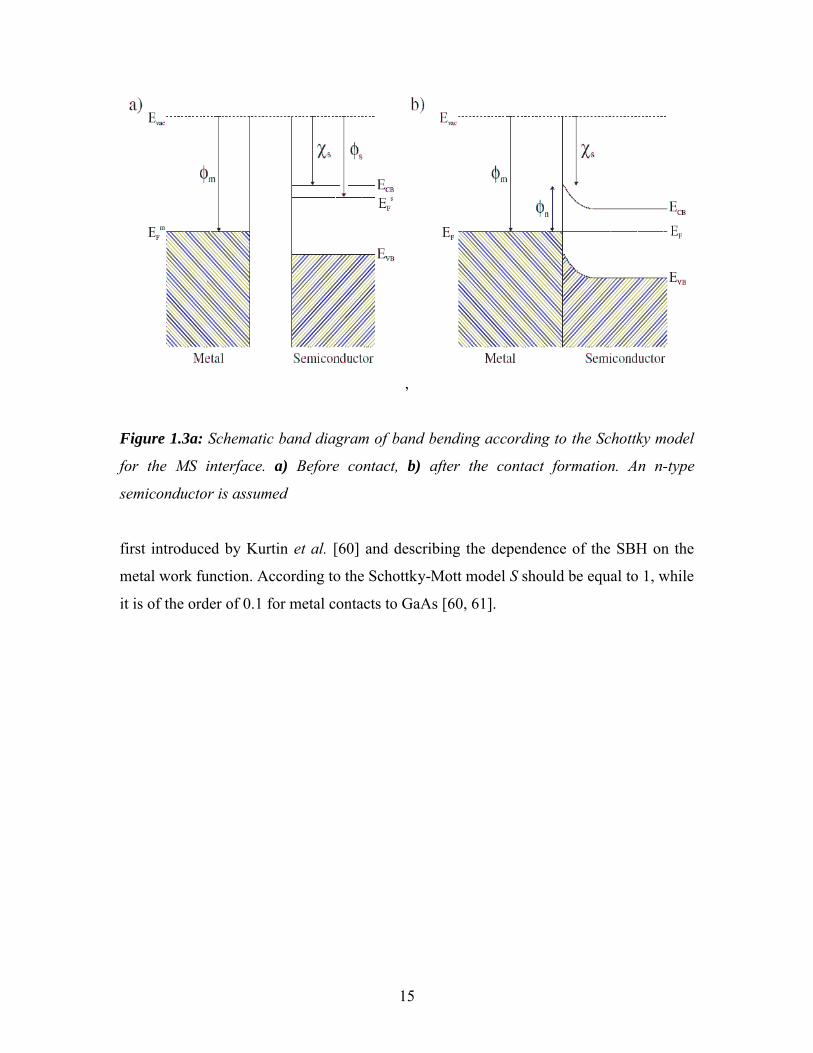
barrier formation was proposed independently in 1938 by Schottky [58] and Mott [59].
Fig 1.3a illustrates the band diagram of Schottky’s Gedankenexperiment illustrating the
formation of a Schottky barrier. The metal and the semiconductor are supposed to be
electrically neutral, separated from each other and without any surface charge. We
consider the case of an n-type semiconductor with electron affinity χs and work function
φs, smaller than the metal work function φm. When the metal and the semiconductor come
in electrical contact, the two Fermi levels are forced to coincide and electrons pass from
the semiconductor into the metal. The result is an excess of negative charge on the metal
surface and a negative charge depletion zone in the semiconductor near its surface. These
excess charges form an interface dipole and produce an electric field, directed from the
semiconductor to the metal. By bringing the metal and the semiconductor closer together,
the gap between the two materials vanishes and the electric field corresponds now to a
gradient of the electron potential in the depletion layer, resulting in the well known band-
bending regime. The Schottky-Mott model leads to a n-type SBH φn given by,
smn
And, therefore, depends linearly on the metal work function. However, experimental
results as those presented in Fig. 1.3b for GaAs do not confirm this relationship since the
SBH depends only weakly on the metal work function. Deviation from the Schottky-Mott
behavior are very often measured in terms of the slope parameter,m
n
d
dS
15
,
Figure 1.3a: Schematic band diagram of band bending according to the Schottky model
for the MS interface. a) Before contact, b) after the contact formation. An n-type
semiconductor is assumed
first introduced by Kurtin et al. [60] and describing the dependence of the SBH on the
metal work function. According to the Schottky-Mott model S should be equal to 1, while
it is of the order of 0.1 for metal contacts to GaAs [60, 61].

16
Figure 1.3b: Barrier height at metal/GaAs as a function of metal work function [62]
Figure 1.3c: Barrier height at metal/n-Si as a function of metal work function.
An important limitation of the Schottky-Mott model is the neglect of surface states. This
prompted Bardeen [63] to propose in 1947 a different model. He showed that if the

17
density of localized states [64, 65] having energies distributed in the semiconductor
energy gap is sufficiently high, double layer at the free surface of a semiconductor is
formed from a net charge of electrons in surface states and a space charge of opposite
sign. He concluded that this double layer will tend to make the work function
independent of the height of the Fermi level in the interior of the semiconductor, and the
rectification characteristics or barrier height at the metal-semiconductor contact are then
practically independent of the metal (Figure 1.3d). In this extreme case, the SBH does
not depend at all on the metal work function, i.e. S = 0 when surface states are present.
All models of MS interfaces proposed afterwards are essentially generalizations of these
two basic models. In the following section we discuss the phenomenological formula for
n-SBH derived by Cowley and Sze in 1965 [66]. This formula is valid as long as the
Fermi level pinning of SBH is described by the presence of interface gap states. These
interface gap states may be of the nature of semiconductor surface states, metal induced
gap states (MIGS) [67], defect states [68] and/or disorder induced gap states [69]. We
will also discuss how the polarized bonds at the interface can lead to apparent Fermi level
pinning effect [70].
Figure 1.3d: Schematic band diagram of band bending according to the Bardeen model
for the MS interface. a) Before contact, b) after the contact formation. The Fermi level is
pinned by a high density of surface states of the semiconductor.

18
1.3.1 Theory of SBH in presence of surface states
The energy band diagram of a metal–n type semiconductor contact is shown in
Figure 1.3.1a. We assume that the contact between metal and semiconductor has an
interfacial layer of the order of atomic dimensions and surface states density (per unit
area per eV) at the interface is a property only of the semiconductor surface and is
independent of the metal. The energy φ0 is measured from the valence band edge at the
semiconductor surface and specifies the level below which all surface states must be
filled for charge neutrality at the semiconductor surface. This is also called the charge
neutrality level (CNL). The quantity φBn is the n-SBH at metal semiconductor contact
and Δφn is the image force lowering of the n-SBH [37]. The interfacial layer is assumed
to have a thickness of a few angstroms and will be assumed transparent to electrons
whose energy is greater than the potential barrier.
Figure 1.3.1a: Energy band diagram of a metal- n-type semiconductor contact with an
interfacial layer. φm is the work function of metal; φBn is the n-SBH of metal-

19
semiconductor surface barrier; φ0 is the charge neutrality level; Δφn is the image force
barrier lowering; φn is the energy difference between conduction band and Fermi level in
the semiconductor; Δ0 is the potential across interfacial layer; χ is the lectron affinity of
semiconductor; VB0 is the diffusion potential; εs and εi are the dielectric constant of
semiconductor and interfacial layer; δ is the thickness of interfacial layer; Qss is the
surface charge density on semiconductor; Qm is the surface density on metal [66].
We consider a semiconductor with acceptor surface states whose density is Ds
states/cm2/eV and assume that Ds is constant over the energy range from φ0 to the Fermi
level. For a uniform distribution the surface state charge density on the semiconductor Qss
is given by
,/)( 20 cmCEeDQ nBngsss (1.3.1 a)
The quantity in parentheses is simply the difference between the Fermi level at the
surface and φ0 .Ds times this quantity yields the number of surface states above φ0 which
are full. The space charge which forms in the depletion layer of the semiconductor can be
expressed as an equivalent surface charge density, which is the net charge/cm2 looking
into the bulk semiconductor from a point just inside the semiconductor surface. The
charge is obtained by solving Poisson’s equation for the depletion layer of the
semiconductor and can be written as
,/)/(2 22/1 cmCekTNeQ nnBnDssc (1.3.1b)
where ND is the donor density of the bulk semiconductor. The equivalent surface charge
density on the semiconductor surface is given by the sum of Eqs. (1.3.1a) and (1.3.1b). In
the absence of any space charge effects in the interfacial layer, an exactly equal and
opposite charge Qm. develops on the metal surface. For thin interfacial layers, such effets
are negligible, and Qm be written as
2/10 )/(2)()( ekTNeEeDQQQ nnBnDsnBngsscssm
(1.3.1c)
The potential Δ0 across the interfacial layer with no voltage applied to the junction can be
obtained by the application of Gauss’s law to the surface charge on the metal and
semiconductor:

20
),/(0 imQ (1.3.1d)
where εi is the dielectric constant of the interfacial layer and δ its thickness. Another
relation for Δ0 can be obtained by inspection of the energy band diagram of Figure 1.3.1a:
),(0 nBnm (1.3.1e)
These results from the fact the Fermi level must be constant throughout the metal-
interfacial layer-semiconductor system at equilibrium. If Δ0 is eliminated from Eqs.
(1.3.1d) and (1.3.1e), and Eq. (1.3.1c) is used to substitute for Qm , we obtain
nBngi
snnBn
i
DsnBnm E
eDekT
Ne
0
2/1
2
2
/2
)()(
(1.3.1f)
Equation (1.3.1f) can now be solved for φBn. Introducing the quantities V1, α, and γ
221 /2 iDs NeV ; iseD / ; )/()1/(1 sii De ; (1.3.1g)
Equation (1.3.1f) can be written as
2/1
211
1012/31
20
4///
2/12/)(1
VekTV
VEVVE
n
gm
ngmBn
(1.3.1h)
Equation (1.3.1g) can be used to calculate V1 if values of δ and εi are estimated: For
vacuum-cleaved or well cleaned semiconductor substrates the interfacial layer will have a
thickness of atomic dimensions, i.e., 4 or 5 Ǻ. The dielectric constant of such a thin layer
can be well approximated by the free space value, and since this approximation
represents a lower limit for εi , it leads to an overestimation of V1 .For εs ~ 10 εi and ND <
1018 cm-3 , V1 is small, of the order of 0.01 eV, and the term in the curly brackets in Eq.
(1.3.1h) is estimated to be less than 0.04 eV. Neglect of this term in Eq. (1.3.1h) reduces
the equation to
ngmBn E 01 , (1.3.1i)
where
12
1
i
sDe

21
The γ in Eq. (1.3.1i) is the theoretical slope parameter and is often compared with
experimental slope parameter S. Moreover, the symbol S is also used for γ in the
literature. The experimental values of γ, φ0 , and Ds for different semiconductor systems
can be obtained by fitting experimental values of φBn with Eq. (1.3.1i). For silicon, γ, φ0,
and Ds were obtained to be 0.27±0.05, 0.30±0.36 eV, and 2.7±0.7 ×10¹³ states/cm2/eV
[32]. For GaAs, γ, φ0, and Ds were obtained to be 0.07±0.05, 0.53±0.33 eV, and
12.5±10.0 ×10¹³ states/cm2/eV.
1.3.2 MIGS, Defect states and Disorder induced gap states models
Heine in 1965 [67] showed that localized surface states as assumed by Bardeen
[64] and Cowley and Sze [66], can not exist at the metal-semiconductor interface.
However resonance surface states or metal induced gap states (MIGS) can exist which
behave for the practical purposes in the same way. This follows from simple
considerations of matching the wavefunctions the metal-semiconductor boundary. For an
energy E below Fermi energy in the gap of the semiconductor, the solutions of the
Schrodinger equation will decay exponentially in the semiconductor but propagate as
Bloch states on the metal side of the junction to form the ordinary states of the metal. If
the x-axis is taken as perpendicular to the surface then for some value of k = k|| parallel to
the surface, e.g., ky = kz = 0, we have the bands shown in Fig. 1.3.2a . At energy E, the
exponential solution in the semiconductor can always be joined onto the two Bloch states
with wave vector ensuring that both ψ and its derivative can be matched at the boundary.
Thus for energies in the semiconductor band gap of the states of the metal all have tails in
the semiconductor.

22
Figure 1.3.2a: An energy E of a surface state in the band gap of the semiconductor
corresponds to two propagating Bloch functions k1, -k1 in the metal.
Thus resonance states or MIGS are basically the tails of metal wavefunction rather than
separate states in the band gap of the semiconductor and Bloch states of the bulk
semiconductor with complex wave vector. Since the MIGS are split off from the valence
and the conduction band, their character varies across the gap from mostly donor type
close to the top of the valence band to mostly acceptor type close to the bottom of the
conduction band. The charge transferred between the metal and the semiconductor then
pins the Fermi level above, at, or below the charge-neutrality level φ0 of the MIGS when
the electronegativity of the metal is smaller, equal to, and larger than, respectively, the
one of the semiconductor. Eq. (1.3.1i) still describes the dependence of n-SBH on metal
work function. Monch [51] realized that the slope parameter γ (or S) in the MIGS model
(Eq. 1.3.1i) depends only on the product of the density of states (Ds) around the charge
neutrality level and the width δ of the related dipole layer which is determined by the
average band-gap energy of the semiconductor. On the other hand the band-gap of the
semiconductor is related to the electronic polarizability (ε∞-1). As apparent in Figure
1.3.2b, the S values of nineteen different semiconductors follow a pronounced chemical
trend when (1/S -1) is plotted over (ε∞ - 1). A least-square fit to the data yields
211.01
1
S , (1.3.2a)

23
Figure 1.3.2b: Slope parameter S plotted versus the electronic contribution ε∞ of the
dielectric constant of the semiconductor.
In 1984, Tersoff [71] suggested a method to calculate the charge neutrality level in the
MIGS model. He suggested that the charge neutrality level can be associated with the
branch point of the complex band structure in the fundamental gap since MIGS are
actually Bloch states of the bulk semiconductor with complex wave vector and charge
neutrality level must fall at or near the energy where the gap states cross over from
valence to conduction band character. In one dimension this energy corresponds to the
branch point of the complex band structure [72]. The branch point in the fundamental gap
coincides with the zero of the cell-averaged real-space Green’s function calculated along
a judiciously chosen crystallographic direction:
kn kn
xki
iEE
eExG
, ,
0,
Here E is the energy in the fundamental gap, and a small imaginary term iη in the
denominator insures convergence. The direction x should be chosen to give the slowest
decaying evanescent state. To calculate the branch point from the actual calculation of the
complex band structure, the band energy En(k) is considered as a multi-valued function
E(k) of a complex wave vector k = g + ih . The usual band structure is then the Re(E) – g

24
cross-section of the Reimann surface. Starting at the lower energy surface (e.g., the
valence band) and going into the complex k-plane around the branch point and back we
end up on the next energy surface (i.e., the conduction band). Solutions of the
Schrodinger equation with the energy in the band gap thus have complex wave vectors,
and are therefore spatially decaying. The character of the solution continuously changes
from that of the lower energy band to higher energy band, with branch point serving as a
point of cross-over from donor-like states to acceptor-like states. The physical connection
between the wave vector at a branch point and the interface dipole was first made by
Heine [67], who used its inverse (the penetration dept of the evanescent gap state) to
estimate the separation of the positive charge in the metal and negative charge in the
surface states. The dipole is D = 4πσt/ε, where σ is the charge density per unit area, ε is
the dielectric constant, and t = 1/q is the mean separation between the negative charge in
the surface states and the positive charge in the metal. Here q is the imaginary wave
vector describing the complex band structure in the forbidden energy gap of the
semiconductor. When the wave functions are matched at the metal-semiconductor
interface, the evanescent wave describes the exponential decay of the metal wave
function inside the semiconductor. In other words the metal effectively charges the
imaginary wave vector states rather than induces them. Note that the complex band
structure is a bulk property of a material, and thus can be calculated without a detailed
interface model.
Models based on defect states and disorder induced gap states (DIGS) have also
been proposed to explain Fermi level pinning at metal-semiconductor interfaces. The
defect states model proposed by Wieder [73] and Spicer [68] et al identifies the interface
states at the metal-semiconductor contacts as electronic states of native defects which are
created during the formation of the junction. The defect states model was motivated by
the observations that Schottky barriers on III-V compound semiconductors were found to
be insensitive to within 0.2 eV to the metals used and to follow no apparent chemical
trend. The DIGS model proposed by Hasegawa et al [69] was used to explain the
observed Fermi level pinning and correlation between the insulator-semiconductor and
metal-semiconductor interfaces.

25
1.3.3 Limitations of the MIGS model
The MIGS model has been applied to the analysis of SBHs observed at a variety
of metal-semiconductor interfaces to deduce MIGS densities [74]. Despite large scatter in
the experimental data, reasonable agreement can usually be found for most
semiconductors with predictions based on interface gap states, i.e., Eq. (1.3.1i). The
widespread application of the MIGS model and its apparent success in the analysis of
experimental data belie the fact that several major assumptions of the MIGS model have
been shown to be without the basis. Experimental data from epitaxial metal-
semiconductor interfaces have shown that the SBH depends on the interface atomic
structure [75]. Calculations further showed that the distribution of the MIGS depends
strongly on the interface structure [70] and that the charge neutrality condition of the
interfacial semiconductor could not be determined by the distribution of electronic states
within the fundamental gap alone due to the presence of surface states elsewhere in the
semiconductor [76]. Furthermore, it was pointed out [77] nearly two decades ago that
MIGS or any other model which assume the interface states to be in thermal equilibrium
with only the semiconductor could not be reconciled with the nearly perfect ideality
factors observed in current-voltage (I-V) experiments. These facts suggest that even
though MIGSs are present at every MS interface, they do not lead to an interface dipole
in the fashion assumed by existing models and explicitly expressed in Eq. (1.3.1.i).
Theoretical and experimental work on epitaxial metal-semiconductor interfaces
show that the SBH between the same metal-semiconductor pair can vary by more than
one third of the band gap, with a mere change in the interface structure [78]. This finding
suggests first that the SBH at nonepitaxial metal-semiconductor interfaces could be
inhomogeneous, a fact which has often been found to be true in experiments [70]. At the
same time, a structure-dependent interface dipole also seems to suggest that the SBH
likely depends sensitively on the choice of the metal, in conflict with the observed Fermi
level pinning effect. Why the SBH which depends so critically on the structure of
epitaxial interfaces should appear to assume nearly constant values for polycrystalline
metal-semiconductor interfaces is still an unanswered question. Given the discussion
above concerning MIGS model’s fundamental problems, the question becomes “If not

26
gap states, what else can lead to relationships like Eqs. (1.3.1i)?. Recently Tung [70] has
showed quantitatively that chemical bonding at the metal-semiconductor interfaces can
lead to the apparent Fermi level pinning effect and is a primary mechanism of the
Schottky barrier height. In the following we derive the formula like Eq. (1.3.1i) but with
chemical bonding as the primary mechanism rather than the interface gap states.
1.3.4 Theory of SBH based on the interfacial chemical bonding
When a metal is joined by a semiconductor, and thermodynamic equilibrium is
reached, chemical bonding has to take place. At an ordinary, polycrystalline metal-
semiconductor interface, the bonding geometry likely changes from place to place,
leading to a locally varying interface dipole. The measured SBH then reflects some
weighted average of this interface dipole. Because of the randomness of the interface
structure, there is the expectation that the interface dipole can perhaps be estimated using
bulk-derived properties. It therefore makes some sense to analyze the electric dipole at a
metal-semiconductor interface using established techniques in chemical physics,
developed largely for molecular systems. The total energy of a multi-atomic molecule
can be written, neglecting higher order terms, as [79, 80]
A BA
ABBAAAAAANAtot
JQQQYQUEQQE
22
1,..... 20 (1.3.4a)
where EA0 is the energy of atom A in the uncharged state, -eQA is the net charge on atom
A, UA = χA/2 + IA/2 is the Mulliken potential, YA =IA –χA is the idem-potential, and JAB
=e2/ε0 dAB is the Coulombic interaction between two charges which are situated at
atomic positions A and B. In the above, χ is the electron affinity, I is the ionization
potential, and dAB is the distance between atoms A and B. In thermal equilibrium, one can
apply the condition that the chemical potential is a constant for all the atoms in the same
molecule, and be able to estimate the charge transfer between atoms. This approach has
yielded dipoles for small heteronuclear molecules in good quantitative agreement with
experiment [81]. To apply the above method to a metal-semiconductor interface, the

27
conglomerate of the entire metal-semiconductor region can be regarded as a giant
“molecule.” The truncated lattices of a metal and a semiconductor are assumed to form
bonds on an atomically flat interface plane. A density of chemical bonds, NB, is assumed
to form across the metal-semiconductor interface. In general, NB needs not equal, and is
likely less than, the total number of semiconductor (or metal) atoms per unit area on each
plane parallel to the interface. Lattice mismatch, structure incompatibility, interface
mixing, the formation of tilted bonds, etc., all tend to reduce the number of effective
bonds formed across a metal-semiconductor interface. Without loss of generality, we
assume chemical bonds to form in a square array with a lateral dimension of dB = NB-1/2.
We can write a total energy equation for the entire metal-semiconductor system. For
simplicity, we assume Q’s to be nonzero only for those metal and semiconductor atoms
on the immediate interface planes which are involved in the bonding. Furthermore, we
keep only the interactions between charged atoms which are nearest neighbors.
neighnear
jiSSSSMMMM
iMSSM
i iSSSSSMMMMMMS
jIjiii
iiii
QQJQQJJQQ
QYQUEQYQUEE
.
,
2020
2
1
2
1
(1.3.4b)
Now we require the chemical potential of a metal atom at the interface,
ii MMSM QE / , to equal that of a semiconductor atom, ii SMSS QE / . Because
of symmetry, every bonded metal atom at the interface has the same net charge –eQM
and every semiconductor atom has a net charge of +eQM. One thus obtains
SSMSMMSM
MSM JJJYY
UUQ
424
, (1.3.4c)
where we have used the fact that there are four in-plane nearest neighbors. In the spirit of
analyzing charge transfer between two crystals, rather than between atoms, we can let the
atoms acquire bulk characteristics. For a bulk metal, the ionization potential and the
electron affinity are both identified as the work function of the metal, φM. Thus, UM = φM
and YM = 0. For a semiconductor, the ionization potential and the electron affinity, χS,
differ by its band gap, Eg. Therefore, US = χS + Eg/2 and YS = Eg. To account for the fact
that the Coulombic interactions take place inside a solid, screening by the respective
dielectric medium is also assumed. Equation (1.3.4c) becomes

28
g
gSMM E
EQ
2/, (1.3.4d)
where κ is the sum of all the hopping interactions, i.e., MSiBS dede /2/4 22 ,
and dMS is the distance between metal and semiconductor atoms at the interface. The
voltage drop across this interfacial dipole layer can now be calculated to be
g
gSM
i
BMS
E
ENedV
2/int (1.3.4e)
where Vint is related to SBH (φBn) as
inteVsMBn , (1.3.4f)
Combining Eqs. (1.3.4e) and (1.3.4f), one gets
2)(1
22g
gi
BMSSM
gi
BMSBn
E
E
Nde
E
Nde
, (1.3.4g)
2
1 gBSMBBn
E , (1.3.4h)
where
gi
BMSB E
Nde2
1
Equation (1.3.4h) predicts a dependence of the SBH on the metal work function which is
similar to that predicted by interface state models, Eq. (1.3.1i).
In Eq. (1.3.4h), the dielectric constant of the interface region, εi , should have a value
somewhere between the dielectric constant of the semiconductor, ε∞, and that of the
metal, εM (= ∞) . A simple average (εi-1 = εM
-1/2 + ε∞-1/2) leads to an estimate of 2 ε∞. Here
the optical dielectric constant is used because the charge transfer occurs between the
semiconductor and the metal, so there should be little ionic contribution to the screening.
A plot between experimentally observed slope parameter S in the form of [ε∞(1-S)]-1 and
band gap of the semiconductor [82] is shown in Fig. 1.3.4a. According to Eq. (1.3.4h),
the quantity plotted in Fig. 1.3.4a is 2ε0 (Eg + κ)/(edMSNB), which should display a linear
behavior if dMS, NB, and κ do not vary appreciably with semiconductors. Indeed, a
roughly linear relationship is observed, which approximately extrapolates through the
origin, suggesting that, due to screening, κ is small compared with typical band gaps. A
slope of ~0.13 eV-1 is deduced from a linear fit, which yields a dMSNB of ~9 × 106 cm-1.

29
Taking dMS to be 2.5 Å, one gets an NB of ~4 × 1014 cm-2 which is a very reasonable
estimate of the number of available bonds on a typical semiconductor surface. The
polarization of the chemical bonds at the metal-semiconductor interface leads to a weak
dependence of the SBH on the work function and a natural tendency for the SBHs to
converge toward one-half of the band gap, both of which are in agreement with
experimental results. Even though the present theory seems to have captured the essence
of the SBH formation mechanism, it is only an approximation and should not be regarded
as numerically accurate. For numerical comparison with SBH experiments, one should
always rely on first principles calculations for a more accurate treatment of the interface
dipole.
Figure 1.3.4a: Experimentally observed slope parameters S [82] are used to plot the
quantity [ε∞(1-S)]-1 against the semiconductor band gap, Eg.

30
Chapter 2
Methodology
In this chapter we provide a brief discussion of the fundamental equations to
describe the systems of interacting electrons and nuclei; and the fist principle methods
based on the density functional theory (DFT) [83, 84]. Density functional theory is the
most widely used method to calculate the electronic structure of the materials. In
particular, we present the plane wave implementation, using ultrasoft pseudopotentials
[85] and plane augmented wave (PAW) method [86]. Furthermore, we also discuss the
reciprocal space formalism with the use of special k-points, a level broadening technique,
the supercell technique for the non-periodic systems and calculation of surface energies,
work functions, elastic constants and SBH from first principle methods. A more extensive
and detailed discussion of the fundamental techniques and their details can be found in a
large number of textbooks and review articles [87-92].
2.1 Ab-initio calculations
The objective of ab-initio methods is to calculate physical properties of materials
without using any experimental input. These calculations from first principles provide the
macroscopic properties of a given physical system just from the knowledge of the type
and position of the atoms. In particular, using the atomic structure as the only input, the
electronic, mechanical, magnetic and optical properties of a condensed matter system can
be obtained.

31
2.1.1 Fundamental equations for interacting electrons and nuclei
Unarguably, the fundamental equations to describe the matter are based on
general methods of quantum mechanics and statistical mechanics. The starting point for
the theoretical description of any system of electrons and nuclei is the general many body
Hamiltonian of the system. Any material or solid can be described as an ensemble of
electrons and nuclei which are coupled by coulomb interactions. Denoting the nuclear
coordinates by R := {RI | I = 1, …Nn}, the electronic coordinates by r := {ri | i =1,…Ne}
and the conjugate momenta P and p , the Hamiltonian of the system can be written as
),()()()()( rRVrVRVpTPTH neeennen
(2.1.1a)
where Tn and Te are the kinetic energy operators for the nuclei and the electrons. While
Vnn , Vee and Vne are the coulomb interaction operators respectively. If we adopt Hartree
atomic units ħ = me = e = 4π/ε0 = 1, then the operators in the Hamiltonian can be written
as
22
2 II I
nM
T
, 22
2 ii e
em
T
,
JI JI
JInn
RR
eZZV
||2
1 2
,
ji ji
eerr
eV
||2
1 2
,
Ii Ii
Ine
Rr
eZV
,
2
||2
1 ;
In principle, all the properties of the solid can be described if an exact solution of the
many body stationary Schrodinger equation, in terms of many body wavefunction Ψ(r,R)
),(),( RrERrH (2.2.1b)
can be obtained. Once Ψ(r,R) is known, expectation value of any observable can be
obtained as
|
|| OO , where O is an general observable operator .
Then, exact electron density n(r) and ground state energy E can be determined as
|
|)(|)(
rnrn ;
|
|| HE
32
where,
Ni
irrrn,1
)()( is the charge density operator.
However, in reality, it is extremely difficult to solve this equation exactly, even with the
best available computer resources. Hence, there arises need to simplify the equation with
some justifiable approximations without losing desired accuracy in the final results.
2.1.2 Born-Oppenheimer or adiabatic approximation
A first approximation is justified by the fact, that the nuclei are more than three
orders of magnitude heavier than electrons. As a consequence, the time scale of the
nuclear motion is orders of magnitude larger than that of the electronic motion. Thus it
can be assumed that the electrons are always in their instantaneous ground state
determined by the external potential of the nuclei, and that the forces acting on the nuclei
are determined by the instantaneous electronic distribution and the nuclear positions of
the system. The electrons are considered to be dependent merely on the nuclear positions
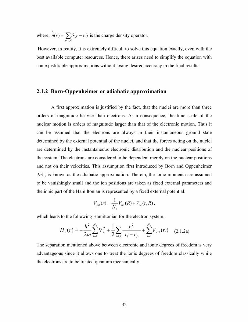
and not on their velocities. This assumption first introduced by Born and Oppenheimer
[93], is known as the adiabatic approximation. Therein, the ionic momenta are assumed
to be vanishingly small and the ion positions are taken as fixed external parameters and
the ionic part of the Hamiltonian is represented by a fixed external potential.
),()(1
)( RrVRVN
rV nenne
ext ,
which leads to the following Hamiltonian for the electron system:
ji
N
iiext
ji
N
iie
ee
rVrr
e
mrH
1
2
1
22
)(||2
1
2)(
(2.1.2a)
The separation mentioned above between electronic and ionic degrees of freedom is very
advantageous since it allows one to treat the ionic degrees of freedom classically while
the electrons are to be treated quantum mechanically.

33
2.2 Density functional theory
Density functional theory [83, 84] is a theory of correlated many-body systems. It
has provided the key step that has made possible development of practical, useful
independent-particle approaches that incorporate effects of interactions and correlations
among particles. As such, density functional theory has become the primary tool for
calculation of electronic structure in condensed matter, and is increasingly important for
quantitative studies of molecules and other finite systems. The remarkable successes of
the approximate local density (LDA) and generalized-gradient approximation (GGA)
functionals within the Kohn-Sham approach have led to widespread interest in density
functional theory as the most promising approach for accurate, practical methods in the
theory of materials. In the following section, we present briefly the fundamental concepts
of DFT. For a more extensive treatment, see [90, 91, 92].
2.2.1 Hohenberg-Kohn theorems
The approach of Hohenberg and Kohn [83] is to formulate density functional
theory as an exact theory of many-body systems. The formulation applies to any system
of interacting particles in an external potential Vext (r), including any problem of electrons
and fixed nuclei, where the Hamiltonian can be written as equa. (2.1.2a). Density
functional theory is based upon two theorems first proved by Hohenberg and Kohn. The
first theorem states that, for any system of interacting particles in an external potential
Vext (r), the potential Vext (r) is determined uniquely, except for a constant, by the ground
state particle density n0 (r) . Since the Hamiltonian is thus fully determined, except for a
constant shift of the energy, it follows that the many-body wavefunctions for all states
(ground and excited) are determined. Therefore, all properties of the system are
completely determined given only the ground state density n0 (r). According to the
second theorem, a universal functional for the energy E[n] in terms of the density n(r) can
be defined, valid for any external potential Vext (r). For any particular Vext (r), the exact
ground state energy of the system is the global minimum value of this functional, and the
34
density n(r) that minimizes the functional is the exact ground state density n0(r). The
Hohenberg-Kohn energy expression for any fully interacting many body system can be
written as a functional of density n(r).
IIextHK ErnrVrdnEnTnE )()(][][][ 3int (2.2.1a)
Where T[n] and Eint[n] are the kinetic energy and interaction energy functional and are
the universal functional by construction. EII is the interaction energy of the nuclei.
2.2.2 Kohn-Sham equations
The Kohn-Sham approach [84] is to replace the difficult interacting many-body
system obeying the Hamiltonian (2.1.2a) with an auxiliary independent-particle system
that can be solved more easily. The Hamiltonian of this auxiliary system is written as
)(2
22
rVm
H effe
aux
; (2.2.2a)
Where Veff (r) is the effective potential seen by an independent electron in the system due
to remaining electrons and nuclei. In this approach, the Hohenberg-Kohn expression of
ground state energy functional (2.2.1a) is written as,
][][)()(][ 3 nEEnErnrVrdnTE XCIIHarteeextsKS (2.2.2b)
Here, n(r), Ts[n], Vext(r), EHartee, and EII are the electron density, independent-particle
kinetic energy, external potential due to nuclei and any other external fields, classical
Coulomb interaction energy of the electron density n(r) and interaction energy of the
nuclei, respectively. Exc is called the exchange-correlation energy and has all the many-
body effects due to exchange and correlation effects in it. If the system has N independent
electrons obeying equa.(2.2.2a), with the ground state having one electron in each of the
N orbitals ψi(r) with the lowest eigenvalues εi of the Hamiltonian, then one can write
expressions for electron density, kinetic energy and Hartree energy as
N
ii rrn
1
2|)(|)( ;
N
iisT
1
2||2
1 ;
||
)()(
2
1][
'
''33
rr
rnrnrrddnEHartree (2.2.2c)

35
The solution of the Kohn-Sham auxiliary system for the ground state is obtained by
minimizing the energy functional (2.2.2b) with respect to the density n(r). Since Ts[n] is
explicitly expressed as a functional of orbitals but all other terms are considered to be
functional of the density, one can also vary the wavefunctions and use the chain rule to
derive the variational equation;
0)(*
r
E
i
KS
, subject to the orthonormalization constraints ijji | .
This leads to the Kohn-Sham Schrodinger-like equations:
0)()( rH iiKS , (2.2.2d)
where the εi are the eigenvalues, and HKS is the effective Hamiltonian
)(2
)( 22
rVm
rH KSKS
,
with )()()()( rVrVrVrV XCHartreeextKS
Equations (2.2.2d) are well known Kohn-Sham equations, with the resulting density n(r)
and total energy EKS given by 2.2.2b. The equations have the form of independent-
particle equations with a potential that must be found self-consistently with the resulting
density. These equations are independent of any approximations to the function Exc[n],
and would lead to the exact ground state density and energy for the interacting system, if
the exact functional Exc[n] were known. The Kohn-Sham equations have to be solved
self-consistently since VHartree and Vxc depend explicitly on the charge density n(r), given
by the eigenstates ψi, which in turn are determined by these potentials. In order to turn
this into practice, an initial guess, e.g. a superposition of atomic charges, is used. On the
basis of the eigenfunctions of (2.2.2d), the new charge density is obtained by summing
over the occupied Kohn-Sham orbitals ψi. Afterwards, the Hartree and exchange-
correlation potentials are then constructed. This process has to be repeated until
convergence is reached. In practice the new charge density is mixed with previous one in
order to avoid numerical instabilities. Figure 2.2.2a gives a schematic overview of the
iterative algorithm.

36
Figure 2.2.2a: Flowchart of self-consistent Kohn-Sham calculation.
Once the effective potential and the charge density become self consistent, forces on the
each ion can be calculated using Hellmann-Feynman [94, 95] theorem. Afterwards, ions
can be optionally moved towards their classical equilibrium positions by minimizing the
effective forces on them. In this way equilibrium geometry of the unit cell can be
determined.
n(r) ; initial guess
Calculate effective potential
VKS[n]=Vext[n]+VKS[n]+VXC[n]
(r)ψε(r)ψ(r)V2m iiiKS
22
N
1i
2
i (r)ψn(r)
Self ConsistentNo
YES
Energy, Forces, Stresses, Eigenvalues, Polarization etc

37
2.2.3 Local density approximation
In order to solve Kohn-Sham equations, one needs to define exchange-correlation
potential. Even though the exact exchange-correlation functional must be very complex,
great progress has been made with remarkably simple approximations. The most simple
and popular approximation to exchange-correlation functional is the local density
approximation [96]. In this approximation, the exchange-correlation energy is simply an
integral over all space with the exchange-correlation energy density at each point
assumed to be same as in a homogeneous electron gas with that density.
)]([)(][ hom3 rnrrndnE xcLDAXC (2.2.3a)
The exchange-correlation energy )]([hom rnXC of a homogeneous electron gas has been
calculated by Ceperley and Alder [97] for various densities using quantum Monte-Carlo
simulations. Perdew and Zunger [98] have parameterized their results in order to
approximate )]([hom rnXC over a wide rage of densities. This procedure is exact if and only
if the density n(r) is constant. If n(r) varies slowly over distances of the order of the
Fermi wavelength, LDA can be expected to provide a good approximation. On the other
hand, at crystalline surfaces or for atoms and molecules, where the electronic density
varies rapidly, the validity of LDA appears to be questionable. Practice shows however,
that LDA yields adequate ground-state properties even for strongly inhomogeneous
systems.
2.2.4 Generalized-gradient approximation (GGA)
The first step beyond the local approximation is functional of the magnitude of
the gradient of the density as well as the value n at each point. In GGA, the functional is
written as a generalized form of the LDA expression:
,......),()()(),.........,()(][ hom33 nnFnrrndnnrrndnE XCXXCGGAXC
Where Fxc is dimensionless and εxchom (n) is the exchange energy of the unpolarized gas.
Numerous forms for Fxc(n) have been proposed. Some of the frequently forms used

38
routinely are, Perdew and Wang (PW91) [99] and Perdew, Burke, and Enzerhof (PBE)
[100].
2.2.5 Discussion
At this point we want to stress that DFT is a ground state theory and that the
Kohn-Sham eigenvalues εi have strictly speaking no physical significance and in
particular, they do not coincide with quasi-particle excitation energies of the real system.
However, it has become standard practice to interpret the εi as estimates of quasi-particle
energies and compare them in solids with experimental band structures. In order to obtain
better approximations of excitation energies, e.g. semiconductor band gaps, a Green’s
function based approach, which is known as the GW approximation, is generally used
[101, 102]. Concerning LDA, we mention that it has some systematic errors. Specifically,
it underestimates semiconductor and insulator band gaps. Furthermore the description of
cohesive energies, weak bonds and of the exchange-correlation potential in the vacuum
region outside surfaces, are generally qualitatively not very accurate. An improvement
over LDA is the semi-local Generalized Gradient Approximation (GGA) which not only
considers the charge density n, but also its gradient Δn. Moreover, it uses non-local
exchange-correlation functionals.
2.3 Application to atomic systems (bulk, surfaces, interfaces etc.)
In the following, we provide a brief overview of the method generally used to
solve the Kohn-Sham equations for condensed matter systems. For crystalline systems, it
is highly beneficial to consider periodic boundary conditions which allow one to expand
the problem into a plane wave basis set, which is highly efficient for a numerical
solution. At first sight, this seems not applicable to surfaces or interfaces, where the
three-dimensional bulk symmetry is broken in one spatial direction. However, as we will

39
discuss later in this section interfaces and surfaces can be investigated with the supercell
technique without loosing the advantages of the plane wave approach.
2.3.1 Plane Wave expansion
Using the Bloch theorem [103], we represent the eigenfunctions ψn,k (r) of the Kohn-
Sham equations as a product of a lattice periodic function un,k (r) and a plane wave with a
wave vector k belonging to the first Brillouin zone (BZ):
Ψn,k (r) = un,k (r) eikr (2.3.1a)
where n is the band index. Since the un,k are by definition lattice periodic, they
can be expanded into plane waves:
'
'
)()( ',,
G
riGknkn eGru (2.3.1b)
Where, G are the reciprocal lattice vectors. For practical purposes the sum in
(2.3.1b) is restricted to plane waves with kinetic energy below a given cutoff energy
Ecut. Thus, defining the set Ω(G):
CutEGkm
GG2
2
2:)(
(2.3.1c)
we obtain the following expansion of the Kohn-Sham wavefunctions:
)(
)(,, )()(
GG
rGiknkn eGr (2.3.1d)
The cutoff energy Ecut controls the numerical convergence relative to the completeness of
the basis set. It depends strongly on the elements which are present in the system under
investigation. The plane wave expansion allows very efficient momentum space
formalism [104]. The Fourier coefficients φn,k(G), obtained by the diagonalization of the
Hamiltonian matrix, contain all relevant information and allow one to calculate all
physical properties of interest, as e.g. the total energy, the Hellmann-Feynman [94, 95]
forces and the stresses [105, 106]. Also the Poisson equation, which defines the Hartree
potential, can be easily solved in reciprocal space.

40
2.3.2 Pseudopotential approximation
Plane waves, which form a convenient and efficient basis set for the diagonalization of
the Hamiltonian, have an essential drawback: they are very efficient in representing
slowly varying functions, but they are not suitable to describe the fast oscillations of
electron wave functions in the core region. In order to overcome this problem the
pseudopotential approximation [107-111] is often used in conjunction with the plane
wave expansion. It exploits the fact that core electrons belonging to closed inner shells
are tightly localized around their nucleus and do not contribute to inter-atomic chemical
interactions. Apart from some exceptions, only valence electrons are influenced by
neighboring atoms. Consequently, they determine the chemical properties. This feature is
the basis of the frozen core approximation used in quantum chemistry. In the
pseudopotential approximation, the influence of core electrons on the valence states is
described by an effective potential. The reduction to the description of only valence
electrons is an essential prerequisite in order to describe large systems containing several
hundred atoms.
Many different schemes have been proposed for constructing pseudopotentials. An
extensive review can be found in Ref. [108]. In the norm-conserving, ab initio
pseudopotentials proposed by Troullier and Martins [112], following properties are
fulfilled:
1. The lowest energy valence pseudo wave-functions generated from the pseudopotential
do not contain nodes.
2. The eigenvalues associated with the exact and the pseudo wave-functions are equal.
3. Beyond a certain cutoff radius rc, the atomic pseudo wavefunctions coincide with the
exact wave functions obtained by an atomic calculation, where all electrons are taken into
account.
4. The charge of the pseudo wavefunctions contained in a sphere of radius rc equals that
of the exact wavefunction.
The quality and transferability, i.e. the independence of the pseudopotential on the given
system, are controlled by the choice of the cutoff radius. A small value of rc corresponds

41
to a high transferability but requires a high energy cutoff to obtain a sufficient numerical
convergence. However, rc has to be larger than the outermost node of all core electron
wave-functions in order to fulfill the norm-conserving criterion 3. In general, the
generation of ‘good’ pseudopotentials, i.e. a good compromise between a sufficient
smoothness of wavefunctions and a good transferability is a time demanding task. The
Troullier-Martins pseudopotentials V TM can be separated into a local part Vloc , i.e. solely
dependent on the distance r, and a non-local part Vlnloc which depends on the orbital
momenta l of the electronic pseudo wavefunctions:
ml
mlnloc
lmllocTM YrVYrVrV
,,. |)()()(
Where, Ylm are the spherical harmonics. In the plane wave expansion with N plane waves,
the matrix elements thus depend on G and G’ and their evaluation therefore scales as N2.
Kleinman and Bylander [113] proposed to transform the non-local components into a
form which allows one to factorize entirely the plane wave integrals:
ml lmllm
llmlmllocKB
V
VVVV
.00
00
||
where δVl = Vloc −Vlnloc and Φlm
0 are the pseudo wave-functions obtained for VTM. In this
form, the evaluation of the matrix elements scales as N and not as N2 as in the original
form which is a significant improvement for large systems. However, the non-locality can
give rise to ghost states [114] which have no physical meaning. By a convenient choice
of the local part, the occurrence of ghost states can be avoided [115].
One goal of pseudopotentials is to create pseudofunctions that are as “smooth” a
possible, and yet are accurate. For example, in plane wave calculations the valance
functions are expanded in Fourier components, and he cost of the calculations scales as a
power of the number of Fourier components needed in the calculation. Thus one
meaningful of definition of maximizing “smoothness” is to minimize the range in the
Fourier space needed to describe the valence properties to a given accuracy. “Norm-
conserving” pseudopotentials achieve the goal of accuracy, usually at some sacrifice of
“smoothness”. In the “ultrasoft pseudopotential” approach, the goal of accurate
calculations is achieved by a transformation that re-expresses the problem in terms of a
smooth function and an auxiliary function around each ion core that represents the

42
rapidly varying part of density. The transformation proposed by Vanderbilt [111] rewrites
the non-local potential in a form involving a smooth function ~~
r that is not norm
conserving. A new non-local potential that operates on the ~
s can now be defined to be
'
''
,,
^
ssssss
US
NL DV ,
where
'''' ,,, sssssssQBD ; drrrrrdrrQQ
CC R
ssss
R
ssss
0
~*~*
0,,
)()()()()( ''''
For each reference atomic states s, it is straightforward to show that the smooth functions
~
s are the solutions of the generalized eigenvalue problem
0~^^
ss SH ,
with US
NLlocal VVH^
2^
2
1 and ^
S an overlap operator,
'
''
,,
^^
1ss
ssssQS ,
which is different from the unity inside the core radius. The eigenvalues εs agree with the
all-electron calculation at as many energies s as desired. The full density can be
constructed from the functions )(',rQ
ss , which can be replaced by a smooth version of
the all-electron density. The advantage of relaxing the norm-conserving condition
0',
ssQ is that each smooth pseudopotential s
~
can be formed independently, with
only the constraint of matching the value of the functions )()(~
cscs RR at the radius
Rc. Thus it becomes possible to choose Rc much larger than for a norm-conserving
pseudopotential, while maintaining the desired accuracy by adding the auxiliary functions
)(',rQ
ss and the overlap operator S.

43
2.3.3 Projector augmented Wave (PAW) method
The projector augmented wave (PAW) method [116] is a general approach to
solution of the electronic structure problem. The PAW approach keeps the full all-
electron wavefunction. Since the full wavefunction varies rapidly near the nucleus, all
integrals are evaluated as a combination of integrals of smooth functions extending
throughout space plus localized contribution evaluated by radial integration over muffin-
tin spheres. In PAW approach, one defines a smooth part of a valence wavefunctions
)(~
rv
i (a plane wave or an atomic orbital), and a linear transformation v
v T~
that
relates the set of all-electron valence functions )(rvj to the smooth functions )(
~
rv
i . The
transformation is assumed to be unity except with a sphere centered on the nucleus,
01 TT . For simplicity, we omit the superscript v, assuming that the ψs are the valence
states, and the labels i, j. Adopting the Dirac notation, the expansion of each smooth
function ~
in partial waves m within each sphere can be written,
,~~
m
mmc
with the corresponding all-electron function,
m
mmcT ~
,
Hence the full wavefunction in all space can be written
,~~
mmmmc
If the transformation T is required to be linear, then the coefficients must be given by a
projection in each sphere
,|~~
mm pc
for some set of projection operators satisfy the biorthogonality condition,
,''
~~
mmmmp

44
then the one-center expansion ~~~
mm p of the smooth functions ~
equals ~
itself.
The general form of the PAW equations can be cast in terms of transformation T.
For any operator
A in the original all-electron problem, one can introduce a transformed
operator ~
A that operates on the smooth part of the wavefunctions
,1~~
mmmm pT
,~~^~^~^^~
'
'
'' mmm
mmmmm pAApATATA
The expressions for physical quantities in the PAW approach follow from above two
equations.
2.3.4 Brillouin zone integration
For many properties, such as the counting of electrons in bands, total energies,
etc., it is essential to sum over the states labeled by k. The crucial point is that if one
chooses the eigenfunctions that obey periodic boundary conditions in a large crystal of
volume Ωcrystal composed of Ncell = N1 × N2 ×…cells, then there is exactly one value of k
for each cell. Thus in a sum states to find an intrinsic property of a crystal expressed as
“per unit cell” one simply ha a sum over values of k divided by the number of values Nk.
For a general function fi(k), where i denotes any of the discrete set of states at each k, the
average value per cell becomes
),(1
kfN
fk
ik
i
(2.3.4a)
The special property of insulators is that the integrals needed all have the form (2.3.4a)
where the sum is over filled bands in the Brillouin zone (BZ). Since the integrand fi(k) is
some function of the eigenfunctions ψi,k and eigenvalues εi,k, it is a smoothly varying,
periodic function of k. Thus fi(k) can be expanded in Fourier components
45
,)()( T
ikTii eTfkf (2.3.4b)
where T are the translation vectors of the crystal. The most important point is that the
contribution of the rapidly varying terms at large T decreases exponentially, so that the
sum in (2.3.4b) cab be truncated to a finite sum. Special points are chosen for efficient
integration of smooth periodic functions. The single most special point is Baldereschi
point [117], where the integration reduces to a single point. The general method proposed
by Monkhorst and Pack [118] is now the most widely used method because it leads to a
uniform set of points determined by a simple formula valid for any crystal:
,2
123
,, 321
ii
i
iinnn G
N
Nnk (2.3.4c)
where Gi are the primitive vectors of the reciprocal lattice.
Metals present an important class of issues for efficient sampling of the desired states in
the BZ. The Fermi surface plays a special role in all properties and the integration over
states must take into account the sharp variation of the Fermi function from unity to zero
as a function of k. This plays a decisive role in all calculations of sums over occupied
states for total quantities and sums over both occupied and empty states for response
functions and special functions. In order to represent the Fermi surface, the tetrahedron
method [119-121] is widely used. If the eigenvalues and vectors are known at a set of
grid points, the variation between the grid points can always be approximated by an
interpolation scheme using tetrahedra. This is particularly useful because tetrahedra can
be used to fill all space for any grid. Tetrahedron methods are are very important in
calculations on transition metals, rare earths, etc., where there are exquisite details of the
Fermi surfaces that must be resolved.
2.3.5 Supercell technique
The formalism sketched above is very efficient for calculating the electronic
properties of periodic systems. The systems investigated in this work, i.e. interfaces and
surfaces lack periodicity in one direction. This drawback can be overcome considering
periodically repeated thin slabs of alternating materials, i.e. artificial superlattices whose

46
unit cells are called supercells. Depending on the materials and on the physical properties
of interest, these supercells can reach large sizes and contain up to several hundred atoms.
The supercell defines a unit cell with one axis perpendicular to the interface or surface of
interest. The periodic repetition of the supercell leads to an artificial superlattice which
allows one to model an interface if the slabs are sufficiently thick. The required thickness
depends on the two materials forming the interface and on the physical quantities under
investigation, i.e. the interaction between the two slab interfaces has to be sufficiently
small. For each property we are interested in, as for example the Schottky barrier or the
work function, the convergence has to be tested through several calculations with an
increasing number of atomic layers in the slabs. Features related particularly to the finite
slab thickness are known as quantum size effects. In this work we normally use 17 atomic
layers for the semiconductor and up to 13 atomic layers for the metal, or vacuum, in the
case of surfaces, respectively.
2.3.6 Band structure alignment and Schottky barriers
To understand the issues involved in the band-lineup problem, we consider two
semiconductors, A and B, with different bandgaps EgA and Eg
B, and bring them together at
an interface. Since the bandgap is discontinuous, it is clear that the valence and/or
conduction bands will also be discontinuous, as illustrated in Fig. 2.3.6a. Note that the
bands on either side of the interface are depicted as flat, corresponding to the notion that
we are only interested in a region on the order of a few atomic distances around the
interface, and that band bending is negligible on this length scale.

47
Fig. 2.3.6a: Schematic illustration of the band structure lineup problem between
semiconductors A and B. The positions of valence and conduction bands are indicated,
all referred to their appropriate reference level
V in each semiconductor. The distance
between
AV and
BV determines the band lineup.
Various theoretical methods are capable of calculating the band structure of a
semiconductor; the interface problem amounts to finding a way to line up the two band
structures across the interface. The band structure of semiconductor A can be calculated
relative to a reference level (usually an average of the electrostatic potential)
AV .
Similarly, the band structure of semiconductor B is referred to a level
BV . For instance,
the position of the valence-band maximum, Ev , is a distance Ev -
V above the position of
the average electrostatic potential (see Fig. 2.3.6a). The band offset problem then consists
of determining the difference in average electrostatic potentials between A and B, i.e.
V . The problem would thus be solved if we could determine the positions of the
average electrostatic potentials inside A and B on an absolute energy scale, e.g. with
respect to the vacuum level. It may seem that if one is able to carry out the band structure

48
calculations for the two semiconductors, then the problem is solved, since these
calculations will provide information about the position of
AV and
BV . Unfortunately
this is not so. The problem is that there is no absolute reference for the average potential
in an infinite solid. This problem is caused by the long-range nature of the Coulomb
interaction, which makes the average potential of an infinite system ill-defined [122]. The
fact that the average potential in an infinite solid is ill-defined is often described
associating single particle-energies with "removal energies". Since in an infinite system
there is no "elsewhere" (e.g., a vacuum level) to remove an electron to, it would seem to
follow that the single-particle energies in the infinite semiconductor cannot be put on an
absolute energy scale. This argument is incomplete, if not wrong, as was pointed out by
[123]. If the interactions were finite in range, the average potential inside a macroscopic
but finite sample would actually not depend on the shape of the solid or surface effects,
and would therefore have a well-defined thermodynamic limit. It is precisely the long
range nature of the Coulomb interaction that causes the removal energies to depend on
the detailed structure of the surface. Or, in the case of an interface, it is the long-range
nature of the Coulomb interaction that causes the presence of a dipole at an interface to
shift the energy levels throughout the semi-infinite solid on either side. It follows that a
band structure calculation for an individual solid cannot provide information about the
absolute position of the average potential. To calculate a band lineup, one has to obtain
additional information about the behavior of the potentials in the neighborhood of the
interface. This indicates that, at least in principle, the details of the atomic structure near
the interface may affect the potentials far away and hence the band-lineup. We thus have
to accept that when we study a bulk semiconductor, the average electrostatic potential
inside the solid is not known on an absolute energy scale, but is defined only to within an
arbitrary constant. This arbitrary constant can be fixed by making specific assumptions
about the boundary conditions. In order to solve the heterojunction problem, an obvious
approach is to specify the boundary condition to be exactly that at the semiconductor
interface, i.e., to perform a calculation in which both semiconductors are present and
joined at the junction. This ensures that the electrostatic potentials of both materials are

49
expressed with respect to the same reference, and allows direct extraction of
V and
thus of the band discontinuities [124].
The mathematical approach used in the first principles calculations with in the
framework of density function theory typically assumes periodicity. For an interface
problem, periodicity can be maintained by considering a superlattice structure, in which
layers of the two semiconductors are periodically repeated. Besides directly providing
useful information about actual superlattice structures, this approach also yields results
for isolated interfaces, provided the layers are sufficiently thick to ensure adequate
separation between adjacent interfaces. Experience has shown that to extract band offsets
layers of eight to sixteen atoms thick typically are sufficient; charge densities and
potentials indeed typically converge quite rapidly to their bulk value away from the
interface. It is then possible to identify a "bulk-like" region in the middle of each
superlattice layer, where the value of an average potential can be determined. For the
purpose of deriving the band-lineup, we are only interested in the behavior of the
potential as we move perpendicular to the interface; the remaining two coordinates can be
eliminated by averaging in planes parallel to the interface:
S
dxdyzyxVS
zV ,,1
, (2.3.6a)
where S represents the area of a unit cell in the plane of the interface. We are then left
with a one-dimensional function, which still exhibits periodic variations in the direction
perpendicular to the interface. This function rapidly recovers its bulk behavior in each of
the two materials comprising the junction as one moves away from the interface;
however, the positions of the average potentials in the bulk-like regions are shifted with
respect to one another, providing exactly the quantity
V that we needed to obtain the
band-lineup. Indeed, separate bulk calculations for the two semiconductors can be carried
out, providing information about individual band positions with respect to the average
potential
V . This procedure for obtaining band offsets is actually similar to that followed
empirically in X-ray photo spectroscopy (XPS) determinations of the offsets. In XPS,
typically, the separation between two representative core levels is measured across the
interface; independent measurements on bulk samples are performed to obtain the energy
50
separation between the valence-band maximum and the core levels in each material. The
core level separation is then used to line up the valence bands and obtain the band offsets.
All-electron calculations can actually mimic this approach, and provide information
about core-level lineups as well as band offsets [125]. Pseudopotential calculations
cannot directly provide core level lineups, since the core electrons are removed from the
problem. However, using average potentials for the lineup is very similar in spirit. It is
important to acknowledge that in density-functional theory the calculated eigenvalues do
not necessarily correspond to quasiparticle energies. A well known consequence of this
deficiency is the failure of density-functional theory to produce the correct band gaps. It
is therefore important to realize that corrections beyond density-functional theory may be
necessary to obtain the exact band positions (with respect to the average electrostatic
potential). We also note, however, that the calculated potential lineup term (
V )
depends only on the charge density of the heterojunction, and as such is a ground-state
property that is reliably given by density-functional theory. The corrections to LDA are
therefore limited to the positions of the quasiparticle energy levels that are obtained in
bulk calculations for the individual materials. Quasiparticle calculations of this nature
have been carried out for a wide variety of semiconductors [126]; by comparing the
results with LDA band structures, it was found that the average LDA error in the
heterojunction valence-band offset was about 120 meV. However, these errors do not
enter if one is only interested in changes in the band offsets (induced by changes in the
interfacial composition and structure), which will only affect the potential-lineup term.
Important information about the heterojunction interface can also be obtained from the
qualitative and quantitative discussion of an interface dipole which is defined properly.
One definition that is often used, in particular in connection with first-principles
pseudopotential calculations, is the following [127]: suppose one takes the difference
between the charge density at the interface (obtained from a supercell calculation, and
averaged in planes parallel to the interface), and the charge density in the bulk (similarly
averaged). One can then use Poisson's equation to calculate a dipole. The dipole,
however, is not unique, since it depends critically on where the mathematical surface
representing the interface is chosen. The location of the interface determines that on one
side, the bulk charge density of semiconductor A will be subtracted, and on the other side

51
that of semiconductor B. A different choice of the "mathematical" interface can produce a
very different dipole. In addition, comparison between different interface orientations
makes little sense with this definition. The bottom line is that the concept of interface
dipole is best avoided, unless one specifies explicitly which definition is being used, and
uses the concept only to identify trends between situations which are sufficiently similar
(e.g., same interface orientation) to allow a meaningful comparison. The issue of defining
an interface dipole can be appropriately addressed with the technique of macroscopic
averaging [128]. Usually, the microscopic potentials and charge densities around an
interface fluctuate with a periodicity imposed by the lattice. Concepts such as the
discontinuity in average potentials are actually defined on a macroscopic scale, since they
involve the difference in potential on either side of the junction, and far away from the
interface. These macroscopic quantities can conveniently be extracted by filtering out the
microscopic oscillations, which is most easily accomplished by averaging the
microscopic quantities over a volume corresponding to the unit cell. Looking at a
heterojunction, we know that the average potential will undergo a shift as one passes
through the interface from one semiconductor to the other. The shift in the average
potential is actually a macroscopic quantity, since it can be observed in measurements far
away from the junction. On a microscopic level, however, the potential looks very
complicated because it exhibits a periodic variation on the atomic scale. This periodic
variation is actually irrelevant for the macroscopic quantity (the potential-lineup) that we
are interested in, and we would like to "filter out" these rapid fluctuations in the potential,
and only take into account the variation on longer length scales. This type of filtering is a
familiar concept in classical electromagnetism for instance in the theory of dielectric
polarization. We already know that to extract dipoles and lineups we may perform an
average of the potential in planes parallel to the interface, as defined in Eq. (2.3.6a). The
quantity (
V ) is a one-dimensional function, which still exhibits periodic variations in the
direction perpendicular to the interface. For any microscopic quantity f(micro)(r) one can
define a macroscopic average fmacro)(r) :
rdrfrrwrf micromacro )()( , (2.3.6b)

52
where w(r) is a properly chosen filter function depending on the geometry and on the
characteristics length scale of the problem. Acting directly on the planer average, the
filter function can be chosen simply as
z
a
azw
2
1, (2.3.6c)
where Θ is the one-dimensional step function, giving
2/
2/
1)
az
az
zdzVa
zV , (2.3.6d)
where a is the length of one period in the direction perpendicular to the interface. The
same procedure can be applied to the charge density. The lineup is related to the dipole
moment of the charge profile:
,00
2
dznznze
V
(2.3.6e)
where n0 is the average electronic density of the two bulk materials. This provides an
unambiguous definition of the interface dipole, without having to make any assumption
about the nature of the interface. The macroscopic average defined above relied on the
fact that the periodicity of the microscopic variations would be the same on both sides of
the interface. This assumption obviously is not satisfied in the case of an interface
between lattice-mismatched semiconductors. Nevertheless, the macroscopic average
technique can also be applied between two materials A and B with different periodicities
because of lattice mismatch or even structural differences. In order to recover
macroscopic features in the bulk regions of both materials, one has to filter twice, using
the functions wA and wB appropriate to each material in turn. This double filtering can be
recast in terms of the single filter function
rdrwrrwrw BA
)( , (2.3.6f)
Often, one is not interested in the absolute magnitude, but in changes in the interface
dipole, brought about by some modification of the interface (e.g., the presence of an
interlayer), while the semi-infinite bulk materials on either side remain unmodified. The
experimentally measured change in the band offset can then be directly associated with a
change in the interface dipole. It is then the task of theoretical analysis to try and ascribe

53
this change to a particular modification of the electronic structure, and in the process of
doing so care should be taken in the definition and calculation of any interface dipole.
In supercell calculations, the band offset or Schottky barrier can also be evaluated
directly from the local density of states (LDOS) N(ε, z) defined as
nkknk zzN
,,, , (2.3.6g)
where the sum runs over the bands n and the wavevectors k of the BZ of the supercell,
2
,, rr nknk
and rnk
, is the electronic wavefunction. Far from the interface, on
each side of the junction, the LDOS N(ε,z) converges to the bulk density of states of the
corresponding crystal. The band offset or Schottky barrier can be obtained thus from the
difference between the band edges of the LDOS on the two sides, far from the junction.
The LDOS, however, requires supercell computations with a high number of k points and
a large energy cut-off compared with those needed to determine the charge density and
the potential line-up. In addition, larger supercells have to be used, since the LDOS has a
spatial convergence to the bulk features slower than that of the charge density. As a
result, the LDOS approach is less convenient, in general, than the potential-line-up
approach to determine the band discontinuities.
2.3.7. Thermodynamics of surfaces and calculation of surface energies
In order to predict the stability of surfaces under realistic experimental conditions
[129], it is necessary to consider the nature of the experiments in order to decide which
quantities should be determined from the ab initio calculations. So long as the surface is
in equilibrium with its surroundings, the stability may be determined following standard
thermodynamics [130] from the free energy and the chemical potential μi of each type of
atom ‘i’. The chemical potentials take into account the fact that the numbers of atoms are
conserved in reactions at the surface, so that changes in the total free energy of the
system when a constituent atom is interchanged between the surface and a reservoir can
be determined. By incorporating the appropriate chemical potentials, we can take into

54
account different experimental conditions and predict the stability of different surface
structures. This approach is clearly appropriate when the surface is in equilibrium with
the bulk and other relevant reservoirs. However, there may be other cases in which the
reactions are not in equilibrium and may be governed by rate limiting kinetic factors.
The chemical potential μi is defined to be the derivative of the Gibbs free energy
G = E+PV –TS for a given phase with respect to the number of particles of type i: μi =
dG/dni [130]. Since in equilibrium the chemical potential μi of a given atomic species is
the same in all its phases which are in contact, each μi can be considered as the free
energy per particle in each reservoir for i. For the condensed state (e.g., GaAs surfaces,
bulk GaAs, or bulk Ga or As), the Gibbs free energy is the total energy at zero
temperature plus a negative definite temperature dependent term which involves a simple
integral of the specific heat [130]. The PV term is completely negligible for pressure
considered here. Although the temperature dependent term can be included in principle,
we ignore it in the present work for the following reasons. First, it is not feasible to
calculate the entropies of the various bulk and surface states. Second, the temperature
dependent terms tend to cancel for the relevant differences between the free energies of
condensed states so that their contributions are small. Third, this approximation has been
implicit in all the recent (rather successful) density functional work calculating phase
transitions using only the energy at T = 0. Thus, for condensed phases, we ignore the
temperature dependence and set the chemical potential μ equal to the total energy E per
atom calculated at T = 0.
For gaseous phases, on the other hand, the effect of T and P upon the chemical
potential cannot be ignored. As is well known in gas theory [130], μ depends
logarithmically upon the chemical potential T and P and the large variations in μ can be
used to control the state of the condensed phases in equilibrium with the gas. In general,
the function μi (P, T) is complicated but can in principle be determined experimentally for
any gas. Nevertheless, even without a detailed knowledge of the chemical potentials as a
function of P and T, we can establish ranges for μi (P, T) which are relevant for the
determination of the surface structures under equilibrium conditions. Although the gas
expressions alone permit any value of the μi, there are limits on the allowable range in
equilibrium with all possible phases. In particular, the chemical potential for each
55
element cannot be above that of the bulk elemental phase. It may equal the bulk chemical
potential ( in which case there is in general bulk material present and the surface is in
equilibrium with the elemental condensed bulk phase) or it may be below the bulk
chemical potential (in which case the bulk is not stable and the surface is in equilibrium
with a gaseous phase).
In addition, the bulk solid AB is a reservoir which can exchange atoms with the
surface. If the surface is in equilibrium with the bulk, pairs of A and B atoms can be
exchanged with the bulk, for which the energy is the total bulk energy pair. This requires
that the sum of the μi for A and B equal the bulk energy per pair. It is useful to note that
the bulk energy may be equated to the sum of the energies of bulk A and bulk B minus
the heat of formation ΔHf. (Note that this requirement on the sum of the chemical
potentials is modified if one accounts for the fact that the bulk can exchange unpaired A
or B atoms by creating defects. This effect may be large at very elevated temperature but
is not relevant under usual growth conditions and temperatures where the small number
of bulk defects do not cause gross changes in the surface stoichiometry.) Thus
equilibrium with the bulk leads to the relation
μA + μB = μAB(bulk) = μA(bulk) + μB(bulk) - ΔHf
Finally, making use of the above limits on the individual μi set by the bulk elements, one
finds that the surface can be in equilibrium with its surrounding only if the chemical
potentials are within both upper and lower limits:
μB(bulk) - ΔHf ≤ μB ≤ μB(bulk) ,
μA(bulk) - ΔHf ≤ μA ≤ μA(bulk) ,
The equilibrium state of the surface as a function of composition is determined by
minimizing the function
i i
iiisurfaceiiisurface nnEnnG )()(
Here Gsurface(ni) is the surface free energy as a function of the variable composition and
the approximate equality above amounts to replacing G by the total surface energy E(ni)
at T = 0.

56
2.3.8 Elastic Constants
The elastic constants determine the stiffness of a crystal against an externally
applied strain. For small deformations, we expect a quadratic dependence of the crystal
energy E on the strain (Hooke’s law). The elastic constants cijkl describe this quadratic
behavior. Consider a displacement u(R) which takes every Bravais lattice point R of the
undistorted lattice to a new position R’ in the strained lattice,
Ri’ = Ri + ui(R), (2.3.8a)
where the index i corresponds to Cartesian coordinates. If we assume the applied strain is
homogeneous (uniform throughout the crystal), we can rewrite (2.3.8a) as
j
jiji RR ' with j
iijij R
Ru
)(
(2.3.8b)
For a homogeneous applied strain the displacement gradients ji RRu /)( are simply
constants, independent of R. These displacement gradients define the nine components of
a tensor. However, since the total energy E cannot change under rotations of the crystal
as a whole, E can only depend on the symmetric part of the deformation, [131] called the
strain tensor ε:
i
j
j
iij R
Ru
R
Ru )()(
2
1 (2.3.8c)
Expanding the internal energy E(V,ε) of the crystal with respect to the strain tensor
gives[132]
ij ijkl
klijijklijijmn cV
VVEVE .......2
)(}){,( , (2.3.8d)
where the stress tensor σ is defined by
0
}{,(1
ij
mnij
VE
V’ (2.3.8e)
the second order adiabatic elastic constants are given by

57
0
2 }){,(1
klij
mnijkl
VE
Vc (2.3.8f)
and V is the volume of the unstrained crystal. It is convenient to use Voigt notation which
takes advantage of the symmetries of the tensors: xx1, yy2, zz3, yz4, xz5, and
xy6. Using this notation (2.3.8d) becomes [1311]
.............2
)(}){,( ij
jiiji
iii eecV
eVVEeVE (2.3.8g)
with the strain tensor given by
In order to calculate all M elastic constants of a crystal, M independent strains ε(I) to the
unit cell are applied, using (2.3.8b) and (2.3.8e) to determine the atom positions within
the strained unit cell. For instance, there are M=3 for cubic Si, Ge and Ni, M=6 and M=9
for orthorhombic NiGe. Each strain I = 1, . . . ,M is parameterized by a single variable γ
and the total energy E(I) (γ) is calculated for a number of small values of γ . For these
small distortions, E(I) (γ) is fit to a polynomial in γ and then equated to the appropriate
elastic constant expression E(V,{ei(I)(γ)}) in (2.3.8g). From all of the fits, a system of M
linear equations for the elastic constants are obtained, which are then solved for the cij.
Since the undistorted crystal is generally taken to be the zero-pressure theoretical
equilibrium structure, the applied stress σ is zero and so the second term of (2.3.8d) and
(2.3.8g) does not enter in the calculations described here.
The parameterizations used for the three independent strains in the cubic cases of
Ni and Ge are given in Table 2.3.8a. Strain I =1 is a volume-conserving stretch along the
z axis, the second strain is equivalent to simple hydrostatic pressure, and strain I = 3
e1 e6/2 e5 /2
e6/2 e2 e4/2
e5 /2 e4/2 e3

58
corresponds to a volume-conserving monoclinic shear about the z axis. Calculations for
nine values of γ in the range of -0.01 to 0.01 are carried out for strains 1 and 2. However,
for strain 3, nine points in the range from -0.04 to 0.04 are calculated because the changes
in the energy were rather small (a maximum of 0.1 mRy for γ = 0.01), leading to larger
error estimates in the case of the smaller range. Orthorhombic NiGe has nine independent
elastic constants and the nine strains listed in Table 2.3.8b are chosen. For each of the
silicide strains, calculations for seven values of γ in the range of -0.01 to 0.01 are carried
out.
Strain I Parameters(unlisted ei) ΔE/V to O(γ2)
1 e1 = e2 = γ, e3 = (1+γ)-2-1 3(c11-c12)γ2
2 e1 = e2 = e3 = γ 3/2 (c11+2 c12)γ2
3 e6 = γ, e3 = γ2(4-γ2)-1 1/2 (c44 γ2)
Table 2.3.8a: Parameterizations of the three strains used to calculate the three elastic
constants of cubic Ni and Ge. The energy expressions were obtained from (2.3.8g).
Strains I = 1 and I = 3 are strictly volume-conserving to all orders in the strain
parameter γ. If we restrict ourselves to linear order only then e3(1) = -2 γ and e3
(3) = 0,
with volume conservation preserved to linear order as well.

59
Strain I Parameters(unlisted ei = 0) ΔE/V to O(γ2)
1 e1 = γ 1/2 (c11γ2)
2 e2 = γ 1/2 (c22γ2)
3 e3 = γ 1/2 (c33γ2)
4 e1 = 2γ, e2 = -γ, e3 = -γ 1/2(4c11 - 4c12 - 4c13 + c22 + 2c23 + c33)γ2
5 e1 = -γ, e2 = 2γ, e3 = -γ 1/2(c11 - 4c12 + 2c13+ 4c22 - 4c23 + c33)γ2
6 e1 = -γ, e2 = -γ, e3 = 2γ 1/2(c11 + 2c12 - 4c13 + c22 - 4c23 + 4c33)γ2
7 e4 = γ 1/2 (c44 γ2)
8 e5 = γ 1/2 (c55 γ2)
9 e6 = γ 1/2 (c66 γ2)
Table 2.3.8b: Parameterizations of the nine strains used to calculate the nine elastic
constants of orthorhombic NiGe. The energy expressions were obtained from (2.3.8g).

60
Chapter 3
Electronic structure, surface energies and work functions of PtSi
Metal silicides are used in complimentary metal-oxide-semiconductor (CMOS)
devices to form ohmic contacts with source, drain, and gate silicon because of their low
resistivity, low contact resistance to Si, reasonable thermal stability, and excellent process
compatibility with standard Si technology. Over the past two decades, silicides of Ti, Co
and Ni have been successively used in integrated circuit manufacturing. In the deep
submicron regime NiSi is now succeeding CoSi2. However, both CoSi2 and NiSi exhibit
large (0.5-0.6 eV) Schottky barriers to Si, in addition, NiSi suffers from low thermal
stability. This contact resistance already amounts to a quarter of the total parasitic
resistance, and will clearly only rise as scaling continues. Recently, PtSi has been found
promising to form p-type low resistance contact with Si. It has relatively low (0.2 eV)
Schottky barrier on Si (001) and has excellent thermal stability. With the aid of density
functional theory we study electronic structure, surface energies, and work functions of
PtSi. We also calculate Schottky barrier height (SBH) at Si(001)/PtSi(001) interface. The
rest of the chapter is organized as follows. In the next section, we review the bulk
properties of PtSi. In section 3.2, we report the comprehensive study of surface energetics
and relate it to available data. In section 3.3, we discuss the work functions for several
PtSi orientations, and in section 3.4 we report an estimate of the Schottky-barrier height
at the Si(001)/PtSi(001) interface.

61
3.1 Crystal and electronic structure of bulk PtSi
PtSi crystallizes in the primitive orthorhombic structure in a MnP type lattice with
space group Pnma (# 62 in the International X-Ray Tables) [128, 129] (see Fig.3.1a). In
the standard setting experimental lattice constants are a=5.922 Å, b=5.575 Å and c=3.586
Å. Contrary to references [130] and [131] who used c=5.922 Å, we use the standard
setting. There are four symmetry-equivalent Pt and four symmetry equivalent Si atoms
per primitive orthorhombic cell. There are also four internal in plane parameters, uSi, vSi,
uPt, vPt for Si and Pt atoms.
Figure 3.1a: The orthorhombic unit cell of bulk PtSi. Lattice constants and free internal
in plane coordinates are given in Table 3.1a and 3.1b.
b
c
Pt Si

62
Material a (Å) b (A) C (A)Ecoh
(eV/atom)ΔHf
(eV/atom) Ref.Pt theo. 3.973 5.77
exp. 3.927 5.84 132PtSi theo. 5.986 5.648 3.635 5.84 -0.67
exp. 5.922 5.575 3.586 5.85 -0.62 133Si theo. 5.466 4.61
exp. 5.428 4.63 132
Table 3.1a: Theoretical and experimental lattice constants (in Å); heat of formations (in
eV/atom); cohesive energy (in eV/atom). The experimental standard heat of formation is
given for T=298.15 K.
Table 3.1b: Experimental and calculated free internal in plane coordinates of PtSi. The
Pt atoms are located at [ Ptu , Ptv , 1/4], [(1/2 - Ptu ), ( Ptv , – 1/2), 1/4], [(1- Ptu ), (1- Ptv ),
3/4,] and [(1/2+ Ptu ), (3/2 – Ptv ), 3/4]. While the Si atoms are located at [ Siu , Siv , 1/4],
[(3/2- Siu ), (1/2 + Siv ), 1/4], [( Siu -1/2), (1/2- Siv ), 3/4] and [(1- Siu ), (1- Siv ), 3/4].
Density functional calculations [83, 84] were done using the projected augmented wave
(PAW) [86] pseudopotentials as implemented in the VASP [134] code. The PBE form
[100] of the generalized gradient approximation (GGA) for exchange and correlation was
employed. A standard plane wave basis set was used with the kinetic energy cut off of
350 eV. We used a 16x16x24 k-point mesh in the orthorhombic cell for the Brillouin
zone integration. The calculations are converged to 10-6 eV/cell and the structure was
relaxed until the forces were less than 0.01 eV/Å per atom. Experimental and calculated
PtSi lattice constants and internal in plane parameters are given in Tables 3.1a and 3.1b,
PtSi Ptu Ptv Siu Siv Ref
Experiment 0.1922 0.9956 0.583 0.177 133
Theory 0.1936 0.9945 0.5835 0.1784

63
respectively. In general the agreement between theory and experiment is very good. The
caption to Table 3.1b gives the atomic positions in terms of the internal parameters
Energy bands along the high symmetry directions in the Brillouin zone in a 12 eV
window around the Fermi level are shown in Fig. 3.1b. In Fig. 3.1c we show the total
density of states of PtSi, and in Figures 3.1d and 3.1e, we show the partial density of
states projected onto Pt and Si atoms, respectively. It is clear that the states at the Fermi
level are derived predominantly from the 5d orbitals of Pt. Also it is evident that Pt 5d
orbitals are not localized but extend throughout the entire valence band as has been
originally pointed out by Beckstein et al. [131]. When compared to the total density of
states of bulk Pt metal (shown in Fig. 3.1f) the density of states at the Fermi level in the
silicide is five times lower, suggesting that PtSi is a poor metal. Note that the Fermi level
in PtSi “misses” the high density region of the 5d-orbital manifold. This is due to the fact
that the volume density of d-orbitals in the silicide is almost factor of two lower than that
in Pt, while the silicide retains 70% of the electrons per unit volume. This results in a
lower work function for PtSi, as we will show later. Our results for the electronic
structure of PtSi are consistent with the experimental results [130] and with theoretical
calculations previously reported [130,131].
6.0
7.0
8.0
9.0
10.0
11.0
12.0
En
erg
y (e
V)
г Z T Y г X U R S X
EF
Figure 3.1b: Band energies at the high symmetry k-points in the Brillouin zone for bulk
PtSi.

64
0.00
0.02
0.04
0.06
0.08
0.10
0.12
0.14
-10.0 -8.0 -6.0 -4.0 -2.0 0.0 2.0 4.0
Energy (eV)
DO
S
Figure 3.1c: The density of states of PtSi (in electrons per Å3 per eV). Fermi energy is
indicated by the dashed line.
0.00
0.05
0.10
0.15
0.20
-10.0 -8.0 -6.0 -4.0 -2.0 0.0 2.0 4.0
Energy (eV)
DO
S
d-states
p -states
s-states
Figure 3.1d: The density of states in PtSi (in electrons per Å3 per eV) site projected on Pt
atoms.

65
0.00
0.02
0.04
0.06
0.08
-10.0 -8.0 -6.0 -4.0 -2.0 0.0 2.0 4.0
Energy (eV)
DO
S
p-statess -states
Figure 3.1e: Projected density of states (in electrons per Å3 per eV) of Si in PtSi.
0.00
0.04
0.08
0.12
0.16
0.20
-10.0 -5.0 0.0 5.0
Energy (eV)
DO
S
Figure 3.1f: Density of states (in electrons per Å3 per eV) of bulk Pt.

66
0.00
0.04
0.08
0.12
0.16
0.20
-10.0 -8.0 -6.0 -4.0 -2.0 0.0 2.0 4.0
Energy (eV)
DO
Sd-states
s -states
p-states
Figure 3.1g: The density of states in Pt projected onto Pt sites (in electrons per Å3 per
eV).
3.2 Surface energies of different PtSi surface orientations
We investigate surface energies for (110), (112), (001), (022), (211), (020), (121),
(130), (111), (310), (202), (101), and (200) terminations of bulk PtSi. Calculations are
done with supercells in a slab geometry (See section 2.3.5 on supercells). Symmetric
slabs based on (1×1) surface cells for each termination are used (the lateral lattice
constant is fixed to that derived from the calculated bulk value). Due to a relatively large
cell size a moderate 4×4×1 k-mesh is employed for the Brillouin zone integration. We
have checked the convergence with (6x6x1) and (8x8x1) grids, the energy changes are of
the order of 410 eV/atom. Each supercell is relaxed until the forces reach 0.02 eV/Å or
less.
We try to maintain the thickness of all slabs at about 17-20 Å which translates
into ten to seventeen layers. The smallest (001)-oriented slab contains 44 atoms; the
largest (130)-oriented slab contains 73 atoms. For example, to simulate the PtSi(001)
surface, we use eight layers of vacuum over eleven layers of PtSi(001) (shown in Figure
3.2a).

67
<001><001>
Figure 3.2a: The Simulation cell for the (001)-oriented PtSi surface slab. Larger light
balls are Si atoms, and smaller dark balls are Pt atoms.
The dimensions of the rectangular surface unit cell are 5.99 Å by 5.65 Å. The
PtSi (001)-1×1 surface cell has two Si and two Pt atoms. The unreconstructed surface can
be described as zig-zag PtSi chains running along the shorter cell edge with two
alternating PtSi intra-chain distances of 2.56Å and 2.44Å. Notice that surface Si atoms in
adjacent chains are separated by only 3.456 (compare to 3.84 Å 2nd neighbor distance on
the unreconstructed Si (001) surface). We define the rumpling parameter ir as in Ref.
[135],
,/)( oSii
Ptii dZZr
Where ZPt and ZSi are the z coordinates of the Pt and Si atoms in the ith layer and d0 is the
bulk interlayer distance (Fig. 3.2b). The results for surface rumpling are presented in
Table 3.2a. To measure the average effect of the relaxation on the inter-planar distance in
the direction normal to the slab surface, we define the plane position as the average z
coordinate of the Pt and Si atoms. Thus in the bulk the inter-planar distance is 1.85 Å.
After the relaxation the distance between the top and second layer increased by 5.6 %; the
other inter-planar distances stay practically unchanged. In addition, we observe relatively
large in-plane atomic displacements in the first two surface layers. The Pt and Si atoms
on the first surface layer are displaced by 0.07 Å and 0.11 Å, respectively (see Fig. 3.2c).
We did not consider the possibility of a more complex surface relaxation in a larger
surface cell.
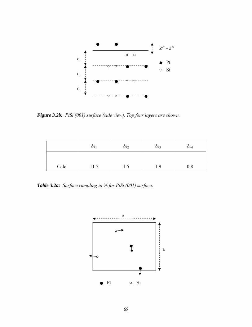
68
Figure 3.2b: PtSi (001) surface (side view). Top four layers are shown.
δr1 δr2 δr3 δr4
Calc. 11.5 1.5 1.9 0.8
Table 3.2a: Surface rumpling in % for PtSi (001) surface.
d
d
d
SiPt ZZ
Pt
Si
Pt Si
c
a
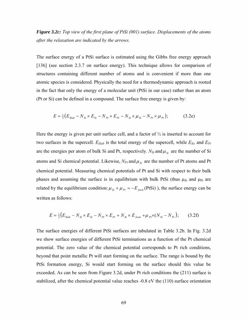
69
Figure 3.2c: Top view of the first plane of PtSi (001) surface. Displacements of the atoms
after the relaxation are indicated by the arrows.
The surface energy of a PtSi surface is estimated using the Gibbs free energy approach
[136] (see section 2.3.7 on surface energy). This technique allows for comparison of
structures containing different number of atoms and is convenient if more than one
atomic species is considered. Physically the need for a thermodynamic approach is rooted
in the fact that only the energy of a molecular unit (PtSi in our case) rather than an atom
(Pt or Si) can be defined in a compound. The surface free energy is given by:
PtPtSiSiPtPtSiSiSlab NNENENEE 21 ; (3.2e)
Here the energy is given per unit surface cell, and a factor of ½ is inserted to account for
two surfaces in the supercell. ESlab is the total energy of the supercell, while ESi, and EPt
are the energies per atom of bulk Si and Pt, respectively. NSi and Si are the number of Si
atoms and Si chemical potential. Likewise, NPt and Si are the number of Pt atoms and Pt
chemical potential. Measuring chemical potentials of Pt and Si with respect to their bulk
phases and assuming the surface is in equilibrium with bulk PtSi (thus μSi and μPt are
related by the equilibrium condition: formPtSi E (PtSi) ), the surface energy can be
written as follows:
PtSiPtformSiPtPtSiSiSlab NNENENENEE (21 ; (3.2f)
The surface energies of different PtSi surfaces are tabulated in Table 3.2b. In Fig. 3.2d
we show surface energies of different PtSi terminations as a function of the Pt chemical
potential. The zero value of the chemical potential corresponds to Pt rich conditions,
beyond that point metallic Pt will start forming on the surface. The range is bound by the
PtSi formation energy, Si would start forming on the surface should this value be
exceeded. As can be seen from Figure 3.2d, under Pt rich conditions the (211) surface is
stabilized, after the chemical potential value reaches -0.8 eV the (110) surface orientation

70
is most stable. Note, that since it is a stoichiometric surface the energy is independent of
the chemical potential. The reactive growth of silicide on Si does occur under Si rich
conditions, and an orthorhombic PtSi(110) peak is always reported [137-139]. On the
other hand (200) which is the highest energy surface considered in this paper, is usually
barely noticeable above the noise level in powder diffraction spectra. Overall, we find
PtSi to have average surface energy, for comparison the surface energy of 2x1-
reconstructed (001) Si is 1700 erg/cm2 [140]. The most important observation, however,
is that under Si rich conditions while (110) is still the lowest energy surface, several
terminations such as (112), (001), (022), and (211) are very close in energy, and are only
200 erg/cm2 higher. Indeed, these are the orientations most commonly reported in the
literature [137-139]. Thus it appears that thermodynamics plays at least as important a
role as kinetics most during the silicide formation. This is an important result, since it
suggests a possibility of controlled silicide growth.
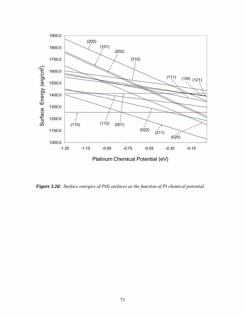
71
1000.0
1100.0
1200.0
1300.0
1400.0
1500.0
1600.0
1700.0
1800.0
1900.0
-1.35 -1.15 -0.95 -0.75 -0.55 -0.35 -0.15
Platinum Chemical Potential (eV)
Sur
face
Ene
rgy
(erg
/cm
2 )
(110)
(020)(211)
(022)(001)(112)
(200)(101)
(202)
(310)
(121)(130)(111)
Figure 3.2d: Surface energies of PtSi surfaces as the function of Pt chemical potential.

72
Table 3.2b: Surface energies (in erg/cm2) and Work functions (in eV) for different PtSi
surface orientations. [a]Experimental value [141].
3.3 Work function at different PtSi surface orientations
The work function m at a metal surface is defined as energy needed to remove
an electron from the bulk to the vacuum just outside the metal [132]. It is generally
known that the work function changes with the orientation of the metal surface by
amounts ranging from one-tenth to one eV. This anisotropy is generally attributed to the
redistribution of the charge density at the surface resulting in a different dipole barrier.
As was first suggested by Smoluchowski [142], there are two competing effects on the
dipole layer which tend to raise and lower the magnitude of the work function. The first
effect is the charge spilling out at the surface resulting in the formation of a negative
dipole layer (dipole pointing inward to the surface) which increases the work function.
Surface Surface Energy ( erg/cm2 ) Work Func. ( eV )
PtSi(001) 1414.02 - 0.0000 µPt 4.96
PtSi(020) 1150.59 - 367.68 µPt 5.18
PtSi(100) 1347.08 - 389.66 µPt 4.99
PtSi(022) 1184.01 - 198.99 µPt 4.89
PtSi(111) 1344.04 - 177.22 µPt 4.86
PtSi(110) 1254.66 - 0.000 µPt 4.97
PtSi(101) 1220.48 - 202.27 µPt 4.97
PtSi(202) 1209.92 - 404.53 µPt 4.95
PtSi(211) 1029.71 - 278.43 µPt 4.98
PtSi(112) 1298.63 - 108.21 µPt 4.81
PtSi(121) 1388.58 - 136.05 µPt 5.00
PtSi(130) 1392.12 - 116.92 µPt 5.02
PtSi(310) 1438.65 - 122.47 µPt 4.72
Pt(111) 5.70, 5.70[a]
73
The second effect is the tendency to smooth out the surface resulting in the formation of a
positive dipole layer which tends to lower the work function. Since these two effects are
comparable in magnitude, the net surface dipole magnitude can only be determined
numerically. Within the DFT-GGA formalism the work function can be readily
calculated in slab geometry as FermiVacm EE . Here VacE and FermiE are the vacuum
energy and the Fermi level. The vacuum energy VacE is estimated by the value of the
total electrostatic potential in the vacuum region separating periodic images of the slab
(Fig. 3.3a). The use of the electrostatic component only is justified since the exchange
potential can be ignored in the middle of the vacuum region where its true value is zero.
The calculated vacuum energy and Fermi energy for the PtSi(001) surface are 9.27 eV
and 4.31 eV, respectively, giving work function of 4.96 eV as shown in Fig. 3.3a.
Calculated work functions for different PtSi surfaces are tabulated in Table 3.2b. The
highest m value is found for the (020) surface and the lowest for the (310) surface, they
differ by almost 0.46 eV. However, both the surfaces are relatively high energy
terminations of PtSi under all thermodynamic conditions. Unfortunately, we know of no
experimental values for the PtSi work functions. To gauge the reliability of our calculated
results we calculated the work function of the Pt (111) surface and obtained m =5.70 eV.
The experimental value reported in the literature for that surface is 5.70 eV [141].
However, for Si(001)-2x1 reconstructed surface, we find the top of the valence band 5.10
eV below vacuum, while the experimental value is 5.27 eV [143]. Thus we believe the
overall accuracy is about a tenth of eV.

74
-10.0
-8.0
-6.0
-4.0
-2.0
0.0
2.0
4.0
6.0
8.0
10.0
0.0 5.0 10.0 15.0 20.0 25.0
Ave
rag
e P
ote
nti
al (
eV) φm = 4.96 eV
EF= 4.31 eV
Evac =9.27 eV
z (Slab axis) (Å)
Figure 3.3a: The planar averaged coulomb potential and work function of the PtSi (001)
surface. Z is the direction normal to the (001) surface.
3.4. Schottky Barrier height at the Si(001)/PtSi(001) interface
In a conventional Schottky model (no Fermi level pinning) (see section 1.3) the n-
type barrier height at the metal semiconductor interface is given by the difference
between the metal work function φ and electron affinity χ of the semiconductor (the
energy difference between the conduction band edge and vacuum) (see Fig. 3.4a).
Likewise, the p-type Schottky-barrier is the difference between the metal work function
and the semiconductor valence band edge, mgE . With the PtSi(001) work

75
function of 4.96 eV and 10.5 gE eV for Si(001), the p-type barrier at the
Si(001)/PtSi(001) interface is 0.14 eV in the Schottky limit. Alternatively, in the Bardeen
limit (strong pinning) the p-type barrier is the difference between the charge neutrality
level ( CNL ) and top of the semiconductor valence band (see section 1.3 on SBH). The
charge neutrality level in silicon is 0.30 eV above the valence band edge [144]. Thus, in
the Bardeen limit the p-type barrier would be 0.30 eV. The barrier height can also be
inferred from the metal induced gap states model (MIGS) model (Fig. 3.4a). The MIGS
interpolates between the Bardeen and the Schottky limits in a linear fashion, and the p-
type barrier p , is given by:
)()( CNLCNLmgp SE ; (3.4b)
Here, CNL is the charge neutrality level measured from the vacuum level and gE is the
valence band gap of the semiconductor and m is the work function of the metal. S is the
empirical pinning parameter describing the screening by the interfacial states [32, 74]
2)1(1.01
1
S ; (3.4c)
Where, ε∞ is the high frequency limit of the dielectric constant of the semiconductor. For
S=0 and 1 one regains the Bardeen and Schottky limits, respectively. Taking ε∞ equal to
11.7 for Si, the S factor is 0.08. Using a value of 3.98 eV for the Si electron affinity
(obtained by adding the measured energy gap to our calculated valence band maximum),
we estimate the p-type barrier to be 0.25 eV, close to the Bardeen limit, as the Fermi level
at the Si surface is strongly pinned.

76
Figure 3.4a: A schematic of the band alignment at the Si(001)-PtSi(001) interface
To perform a first principles calculation of the Schottky barrier we build an
atomistic model of the Si(001)/PtSi(001) interface. We use a supercell composed of
twenty five layers of (001)-oriented Si on top of seven layers of PtSi(001) in a pseudo-
epitaxial arrangement (Fig. 3.4b). The choice of the PtSi orientation is driven by its
typical work function and relatively low surface energy, as well as a reasonable
interfacial structure (see below), and by the cell-size limitations of ab-initio methods.
Assuming the substrate is Si and the film is silicide, the two lateral lattice constants of
PtSi (a and b) are strained by 8% and 3% respectively, to match with the bulk Si lattice
constant. High strain has been suspected in PtSi films on Si (001) [145]. Optimization of
the PtSi lattice constant in the direction normal to the interface results in a 4.9 % increase,
in good agreement with the elasticity theory estimate. We then optimize all the internal
degrees of freedom. Due to high strain we consider this calculation as only an estimate.
However, we find that the work function of PtSi(001) under the same strain is increased
only by 0.08 eV. The energy of our PtSi(001)/Si(001) interface is 1331.9 erg/cm2 not too
different from the PtSi surface energy, thus bonding at the interface appears quite
reasonable, and we believe that the Schottky barrier estimate is relevant. The free energy
of the interface at zero Kelvin is estimated using (3.2f). We set the chemical potential of
Si in the Si side of the cell to zero (assuming equilibrium with the bulk), and since this
PtSi Si
CNL
CB
VB
mχ
Vacuum level
p

77
particular interface is stoichiometric its free energy is independent of the chemical
environment. It is worth noting that the interface energy thus defined is not the energy of
separation. It is rather a measure of “combined unhappiness” of Si atoms in the topmost
layer of Si to see PtSi above them, plus that of PtSi first layer to see a semiconductor
below. The energy thus defined is used when the issues of wetting are of concern [146].
To calculate the Schottky-barrier height we need to know the Fermi level and the Si
valence band edge positions. We follow the procedure originally introduced by Bylander
and Kleinman [147] with the exception that only the average electrostatic potential is
calculated across the supercell (exchange-correlation obtains its bulk value in the centers
of the quantum wells and need not be added). We first compute the planar average of the
potential and then its macroscopic average SiV in the region away from the interface we
believe to be bulk-like. Placing the valence band edge with respect to the macroscopic
average potential requires a separate calculation for bulk Si, where we find the valence
band maximum to be 55.5 refE eV above the reference SiV . In a supercell the average
electrostatic potential and Fermi energy are at 1.17 eV and 7.00 eV, respectively
(Fig.3.4c). Using the bulk reference to locate the valence band top we calculate the
barrier height of 0.28 eV using the formula:
)( refSiFp EVE , (3.2f)
in strikingly good agreement with the MIGS estimate. In addition, we calculate the
barrier height employing ultra-soft potentials with the LDA exchange correlation
functional. This gives the value of 0.16 eV. The agreement between the two methods is
within the accuracy of the calculation.
One can also infer the Schottky-barrier height analyzing the projected density of
states of the Si in Si(001)/PtSi(001) supercell. In this calculation we employ PAW
potentials. Fig. 3.4d shows the density of states projected on s and p states of a Si atom
deep in the Si part of the supercell (where it is expected to regain the bulk like
properties). The top of the Si valence band is a triple degenerate p-state at the Gamma (Γ)
point (if one ignores the spin-orbit coupling). As apparent in Fig.3.2g, the Fermi energy
and Si valence band edge are located at 7.00 eV and 6.69 eV. This gives the barrier
height of 0.31 eV in close agreement with both Bardeen and MIGS predictions owing to

78
the strong pinning character of Si surface. Experimentally for orthorhombic PtSi on p -
type Si (001) the Schottky barrier height is 0.22-0.24 eV, [148], in excellent agreement
with our theoretical estimate.
Figure 3.4b: The Si(001)/PtSi(001) interface structure.

79
-10.0
-8.0
-6.0
-4.0
-2.0
0.0
2.0
4.0
6.0
8.0
10.0
0.0 4.0 8.0 12.0 16.0 20.0 24.0 28.0 32.0 36.0 40.0 44.0 48.0
Av
era
ge
po
ten
tial (
eV
)
Z (Å)
EV = 6.72 eV
EF = 7.00 eV
Фp=EF - EV=0.28 eV
Figure 3.4c: The average coulomb potential (in eV) of Si and PtSi in Si(001)/PtSi(001)
supercell along Z (slab axis).

80
0.00
0.02
0.04
0.06
0.08
0.10
1.0 3.0 5.0 7.0 9.0
Energy (eV)
DO
S
EF = 7.0 eV
EV = 6.69 eV
Фp = EF - EV = 0.31 eV
p- states
s- states
Figure 3.4d: The density of states (in electrons Å3 per eV) site projected on a Si atom
deep inside the Si side of Si(001)/PtSi(001) interface.
3.5 Conclusion
With the aid of density functional theory, we have studied the electronic structure
of PtSi and calculated work functions and surface energies for various surface
terminations. We find that the work function varies by as much as 0.37 eV depending on
the orientation. However, only two terminations considered here result in work functions
significantly different from the typical value of about 4.97 eV. The two PtSi surface
terminations found most stable are (211) under Pt rich conditions, and (110) under Pt
poor conditions. The lower energy terminations identified here are those most commonly
reported in power diffraction spectra. The calculated Schottky barrier height at the
Si(001)/PtSi(001) interface of 1.028.0 eV is in good agreement with available
experiment and corresponds to the Bardeen limit.

81
Chapter 4
Electronic structure, surface energies and work functions of NiGe and PtGe
Unlike metal silicides, metal germanides have not, until recently, attracted much
attention, presumably, due to the lack of practical applications. However, this is about to
change, as scaling of traditional silicon based technology reaches its physical limit, a
germanium channel field effect transistor (FET) is generating a lot of interest. The
germanium channel metal oxide semiconductor FET (MOSFET) offers high mobility of
both carriers (electrons and holes) resulting in higher overdrive current, enhanced
transconductance, and higher cutoff frequencies as compared with a Si transistor.
Historically, the use of germanium has been limited due to the lack of a stable native
oxide and processing technology. Ironically, the emerging use of alternative high-k
dielectrics as the gate insulator in Si-based technology may help finally realize the full
potential of a germanium MOSFET. Nevertheless, to fully exploit transport properties of
germanium, a low resistance contact technology will have to be developed based on
metal germanides, much in the same way that self aligned metal silicides are used in a
standard complimentary metal oxide semiconductor (CMOS) process today. Thus
germanides with low n- and p-type Schottky barriers to the germanium channel (for use
in NMOS and PMOS devices) need to be identified. Germanides are closely related to
analogous silicides in respect to their compositions and structures. In the deep submicron
regime (22 nm and below) NiGe, PtGe and their alloys appear to be promising as low
barrier contacts to p-type germanium. The rest of the chapter is organized as follows. In
the next section, we review bulk properties of NiGe and PtGe. In Sec. 4.2, we report
elastic constants of both the systems. In Sec. 4.3 and 4.4, we report and discuss the
surface energies and work functions for different surface orientations. We further discuss
an unusual surface reconstruction of the NiGe(101)-Ge terminated surface.

82
4.1 Crystal and electronic structure of bulk NiGe and PtGe
Both NiGe and PtGe crystallize in the primitive orthorhombic structure in a MnP
type lattice with space group Pnma (#62 in the international x-ray table) [149-152] (Fig
4.1a). For NiGe, the experimental lattice constants are a = 5.84 Å, b = 5.36 Å, c = 3.50 Å
[149]. The PtGe, experimental lattice constants are a = 6.159 Å, b =5.832 Å, c = 3.754 Å
[150]. There are four symmetry equivalent Ni (Pt) and four symmetry equivalent Ge
atoms per primitive orthorhombic cell of NiGe (PtGe) respectively. There are four
internal plane parameters, uGe, vGe, and uNi (uPt), vNi (vPt). First we perform the
optimization of the orthorhombic cell and internal parameters. Experimental and
calculated NiGe and PtGe lattice constants, cohesive energy and heat of formation are
given in Table 4.1a. The internal in plane parameters are in Table 4.1b, where the caption
gives the atomic position in terms of the internal parameters. The calculated lattice
constants are within 1-2% of reported experimental values.
a
c
bb
Figure 4.1a: The orthorhombic unit cell of bulk NiGe and PtGe. The Yellow and blue
balls are Ge and Ni atoms respectively. Lattice constants and free internal in plane
coordinates are given in Table 4.1a and 4.1b .

83
Material a (Å) b (A) c (A)Ecoh
(eV/atom)ΔHf
(eV/atom)
Ni cal. 3.52 5.40
exp.a 3.52 4.44
Pt cal. 3.93 5.77
exp.a 3.92 5.84
NiGe cal. 5.84 5.36 3.50 4.90 -0.32
exp.b 5.79 5.37 3.43
PtGe cal. 6.16 5.83 3.75 5.18 -0.48
exp.c 6.09 5.72 3.70
Ge cal. 5.75 3.76
exp.a 5.65 3.85
Table 4.1a: Theoretical and experimental lattice constants, heat of formations, and
cohesive energy for Ni, Pt, NiGe, PtGe and Ge. [a] Ref. [132], [b] Ref. [149], [c] Ref [150].
uNi (Pt) vNi (Pt) uGe vGe
NiGe exp. - - - -
cal. 0.1795 0.9933 0.5770 0.1769
PtGe exp.a 0.1908 0.9995 0.5900 0.1850
cal. 0.1922 0.9988 0.5884 0.1857
Table 4.1b: Experimental and calculated free internal in-plane coordinates of NiGe and
PtGe. The Ni (Pt) atoms are located at [uNi (Pt), vNi (Pt), 1/4], [(1/2 - uNi (Pt)), (vNi (Pt) – 1/2),
1/4], [(1- uNi (Pt)), (1- vNi (Pt)), 3/4,] and [(1/2+ uNi (Pt)), (3/2 – vNi (Pt)), 3/4]. While the Ge
atoms are located at [uGe, vGe , 1/4], [(3/2- uGe), (1/2 + vGe), 1/4], [(uGe -1/2), (1/2- vGe ),
3/4] and [(1- uGe), (1- vGe ), 3/4]. [a] Ref. [150]
84
Next we consider the electronic structure of bulk germanides. The energy bands of NiGe
and PtGe along high symmetry directions in the Brillouin zone are shown in Fig. 4.1b
and 4.1c, respectively. In Figs. 4.1d and 4.1g, we show the total density of states of NiGe
and PtGe respectively. In Figs. 4.1e and 4.1f, we show the partial density of states
projected onto Ni and Ge atoms. And, in Figs. 4.1h and 4.1i, we show the partial density
of states projected onto Pt and Ge atoms, respectively. It is clear that the states at and just
below the Fermi level are derived predominantly from the 3d (5d) orbitals of Ni (Pt) in
the NiGe (PtGe) energy bands displayed in Fig. 4.1b and 4.1c. It is interesting to note that
the metallicity of PtGe appears almost accidental. The lower Ge p-derived band near the
Fermi level is occupied only along the -Y direction, and the upper p-derived band
“touches” the Fermi level at Z and along R- direction. Elsewhere along the high
symmetry directions a clear band gap is observed. Charge density contours for NiGe
(001) and Ni (001) planes are shown in Figs. 4.1j and 4.1k. As apparent from Fig. 4.1j,
there appears to be relatively strong three center (Ni-Ge-Ni) covalent bonds between Ni
and Ge atoms in the (001) plane. This is interesting since NiGe is metallic. It is well
known that the bonding of transition metals is almost entirely due to the d-electrons. Thus
it is not unexpected that the Ni-d would hybridize with the Ge-p to form covalent bonds.
This is very similar to the chemical bonding observed in PtSi [130]. The bonding in PtGe
was found to be qualitatively similar to that in NiGe.

85
-12.0
-8.0
-4.0
0.0
4.0
8.0
12.0
Г Y T Z R Г
En
erg
y (
eV
)
EF
Figure 4.1b: Energy Bands of bulk NiGe. The symmetry points are labeled according to
Slater [Ref. 153].

86
-18.0
-14.0
-10.0
-6.0
-2.0
2.0
6.0
Г Y T Z R Г
En
erg
y (e
V)
EF
Figure 4.1c: Energy Bands of bulk PtGe. The symmetry points are labeled according to
Slater [Ref. 153].
0.00
0.04
0.08
0.12
0.16
-5.0 -4.0 -3.0 -2.0 -1.0 0.0 1.0 2.0 3.0 4.0 5.0
Energy (eV)
TD
OS
Figure 4.1d: The total density of states of NiGe (in electrons per Å3 per eV). Fermi
energy is indicated by the dashed line.

87
0.00
0.05
0.10
0.15
0.20
0.25
0.30
0.35
0.40
-5.0 -4.0 -3.0 -2.0 -1.0 0.0 1.0 2.0 3.0 4.0 5.0
Energy (eV)
PD
OS
d-states
p-states
s-states
Figure 4.1e: The partial density of states of NiGe (in electrons per Å3 per eV) projected
onto Ni atoms. Fermi energy is indicated by the dashed line.
0.00
0.02
0.04
0.06
0.08
0.10
-5 -4 -3 -2 -1 0 1 2 3 4 5
Energy (eV)
PD
OS
p-states
d-statess-states
Figure 4.1f: The partial density of states of NiGe (in electrons per Å3 per eV) projected
onto Ge atoms. Fermi energy is indicated by the dashed line.

88
0.00
0.02
0.04
0.06
0.08
0.10
-10.0 -8.0 -6.0 -4.0 -2.0 0.0 2.0 4.0
Energy (eV)
TD
OS
Figure 4.1g: The total density of states of PtGe (in electrons per Å3 per eV). Fermi
energy is indicated by the dashed line.
0.00
0.04
0.08
0.12
0.16
0.20
-10.0 -8.0 -6.0 -4.0 -2.0 0.0 2.0 4.0
Energy (eV)
PD
OS
d-states
s-states
p-states
Figure 4.1h: The partial density of states of PtGe (in electrons per Å3 per eV) projected
onto Pt atoms. Fermi energy is indicated by the dashed line.

89
0.00
0.02
0.04
0.06
0.08
0.10
-10.0 -8.0 -6.0 -4.0 -2.0 0.0 2.0 4.0
Energy (eV)
PD
OS
p-states
d-statess-states
Figure 4.1i: The partial density of states of PtGe (in electrons per Å3 per eV) projected
onto Ge atoms. Fermi energy is indicated by the dashed line.
a
b
Ge
Ni
Figure 4.1j: Valance electron charge density (electrons/Å3) contours in the (001) plane
for NiGe unit cell

90
a
a
Figure 4.1k: Valance electron charge density (electrons/Å3) contours in the (001) plane
for Ni unit cell.
4.2 Elastic constants
Thermal cycling during the Ge process is expected to be gentler than that of the Si
(during the activation of dopants the Si wafer is annealed at temperature in excess of
1000° C). Still a wafer will experience significant thermal stress, and knowing the elastic
constants of germanide crystals is of practical importance. Nine elastic constants are
needed to describe an orthorhombic crystal (compare with only three for a cubic crystal)
[154]. Our elastic constants were calculated by fitting the total energy as a function of
strain to a parabola. The fit is based on six points separated by ~2 meV, and the applied
strain is ~ 1% of the lattice constant. (See section 2.3.8). The experimental and calculated
elastic constants of Si, Ge, Ni, Ge (fcc crystals) are given in Table 4.2a. The theoretical

91
elastic constants and bulk moduli are within 5% of experiment. The calculated elastic
constants of orthorhombic NiGe and PtGe are given in Table 4.2b. Interestingly, despite
the difference in crystal structure and nature of bonding the values calculated for mono-
germanides are remarkably close to simple averages of the Ge and metal values. We have
checked the convergence of the elastic constant C44 with respect to the number of k-
points and plane wave energy cutoff (for NiGe). The value of C44 was raised by 0.7 %
and 2.1 % as the k-point mesh is increased from 6×6×8 to 8×8×12 and 10×10×16. The
C44 value was raised by 0.3 % and 0.4 % as the energy cutoff was increased from 380 eV
to 530 eV and 640 eV respectively. To further check the quality of our calculations we
consider the issue of mechanical stability. The Cauchy conditions for an fcc crystal
restrict the elastic constants in the following way [131]:
(C11-C12) > 0, C11 > 0, C44 > 0, (C11+2 C12) > 0 and C12 < B < C11
Where, B is the bulk modulus. For fcc crystals, such as Ni, Pt, Ge and Si, the bulk
modulus can be calculated as B0 = 1/3(C11+2C12). To ensure the internal consistency we
also calculate the bulk modulus and equilibrium volume by fitting the total energy as a
function of volume to a parabola and a four term Birch-Murnaghan equation of state
[155]:
4
1
3/2)(n
nnVcVE ;
The bulk moduli calculated from the elastic constants, from a parabolic fit and Birch-
Murnaghan fit, in addition to experimental values are given in Tables 4.2a and 4.2b. The
calculated elastic constants of Ge, Si, Ni and Pt lie well within the allowed range for
mechanically stable fcc crystals. Likewise, the elastic constants of mechanically stable
orthorhombic crystals are constrained by the following conditions [131]:
C11 > 0, C22 > 0, C33 > 0, C44 > 0, C55 > 0, C66 > 0, (C11 + C22 -2 C12) > 0,
(C11 + C33 - 2 C13) > 0,
(C22 + C33 – 2 C23) > 0,
(C11 + C22 + C33 + 2 C12 + 2 C13 + 2 C23) > 0, and

92
1/3 (C12 + C13 + C23) < B < 1/3 (C11 + C22 + C33).
For orthorhombic NiGe and PtGe bulk modulus is first calculated as B0 =
1/9(C11+C22+C33+2C12+2C13+2C23) [131]. As evident from Table 4.2b, the calculated
elastic constants of NiGe and PtGe do obey conditions of mechanical stability. The rather
poor agreement (relative to the fcc crystals) between the PtGe bulk modulus calculated
from the elastic constants and the two bulk moduli calculated assuming hydrostatic
pressure, is undoubtedly due to the inner displacements of the atoms and the need to
equilibrate the stresses. That the agreement for NiGe is good may be fortuitous.
Ni[a] Pt[b] Ge[c] Si[d]
C11 cal. 268.4 334.6 124.2 159.8
exp. 261.2 358 131 165
C12 cal. 159.3 247.1 45.9 60.5
exp. 150.8 254 44 63
C44 cal. 131.2 72.2 71.3 75.2
exp. 131.7 77 68.8 79.1
B0 cal.Birch 194.9 272.2 69.9 94.7
cal.parabolic 195.3 275.8 70.8 94.2
cal.elastic 195.7 276.3 72.0 93.6
exp. 187.6 288.4 76.3 97

93
Table 4.2a: Calculated and experimental elastic constants (in the units of GPa) of Ge, Si,
Ni and Pt. Experimental values for Ge, Si, Ni and Pt are extrapolated to 0 K. B0 is the
bulk modulus calculated from elastic constants and from Birch-Murnaghan fit. B0 is
related to elastic constants as B0 = 1/3(C11 +2 C12 ). Superscript indicates the reference
to the experimental values. [a] Ref. [132], [b] Ref. [156], [c] Ref. [157], [d] Ref. [158]
NiGe PtGe
C11 211.69 216.52
C22 183.76 200.57
C33 173.93 206.15
C12 135.70 125.18
C13 99.80 114.42
C23 106.37 113.12
C44 67.20 68.88
C55 106.94 76.02
C66 105.41 53.63
B0elastic 139.24 147.63
B0Parabolic 140.58 153.41
B0Birch 140.94 154.62
Table 4.2b: Calculated elastic constants and bulk modulus (in units of GPa) of NiGe, and
PtGe. B0elastic is the bulk modulus calculated from the elastic constants and is given as
B0elastic = 1/9(C11+C22 + C33 +2 C12 +2 C13+2 C23). B0
Parabolic and B0Birch are the bulk
modulus obtained from a parabolic and Birch-Murnaghan fit.

94
4.3 Surface energy and reconstruction of NiGe and PtGe
We calculated surface energies for (100), (010), (001), (011), (101), (111), (120),
(121), (211) and (021) orientations of bulk NiGe and PtGe for different surface
stoichiometries. To simulate the surfaces, we used supercells in slab geometry of
thickness 14-20 Å (ten to seventeen layers in addition to vacuum layers). For example, to
simulate the NiGe (001) surface, we use eight layers of vacuum over eleven layers of
NiGe (001) (see section 3.2). The smallest (001)-oriented slab contains 44 atoms; the
largest (121)-oriented slab contains 63 atoms. Symmetric slabs based on (1×1) surface
cells for each termination are used (the lateral lattice constant is fixed to that derived
from the calculated bulk value). For the Brillouin zone integration, we use a moderate
4×4×1 Monkhorst-Pack [118] mesh, due to relatively large cell sizes. To check the
convergence we perform calculations with (6×6×1) and (8×8×1) grids, and find the
energy changes are of the order of410 eV/atom. Each supercell is relaxed until the
forces on each atom reach 0.02 eV/Å or less.
Now we describe the nature of reconstruction of the NiGe (001)-1×1 surface. The NiGe
(001) surface has a rectangular surface unit cell of dimensions 5.84 Å by 5.36 Å. There
are two Ge and two Ni atoms in the surface. The unreconstructed surface can be
described as zigzag NiGe chains running along the shorter cell edge (see Fig. 4.3a). We
define the rumpling parameter δri as in [135]
,/)( oGei
Niii dZZr
Where ZNi and ZGe are the z coordinates of the Ni and Ge atoms in the ith layer and d0 is
the bulk interlayer distance (Fig. 4.3b). We also define inter-planar relaxation parameter
δrij as ,/)( ajiij dZZr
Where Zi and Zj are the z coordinates of the ith and jth layer and da is the bulk interlayer
distance. Zi is calculated by averaging the z coordinate of the Ni (Pt) and Ge atoms. The
inter-planar distance in the bulk NiGe is 1.75 Å. The results for surface rumpling and
inter-planar relaxation are presented in Table 4.3a. In addition, we observe relatively
small in-plane atomic displacements in the first two surface layers. The Ni and Ge atoms

95
on the first surface layer are displaced by 0.01 Å and 0.11 Å, respectively. We did not
consider the possibility of a more complex surface relaxation in a larger surface cell.
Figure 4.3a: Top view of the unreconstructed NiGe (001) surface. Blue and yellow balls
are Ni and Ge atoms respectively.
Figure 4.3b: NiGe (001) surface (side view).
d
d
d
GeNi ZZ
Ni
Ge

96
δr1 δr2 δr3 δr4 δr12 δr23 δr34 δr45
Calc. -9.8 2.0 -2.9 0.7 -4.8 0.6 0.0 0.0
Table 4.3a: Surface rumpling and inter-planar relaxation in % for the NiGe (001)
surface. Rumpling parameter δri is defined as ,/)( oGei
Niii dZZr where ZNi and ZGe
are the z coordinates of the Ni and Ge atoms in the ith layer and d0 is the bulk interlayer
distance (Fig.8a). Inter-planar relaxation parameter δrij is defined as
,/)( ajiij dZZr where Zi and Zj are the z coordinates of the ith and jth layer and d0
is the bulk interlayer distance. Zi is calculated by averaging the z coordinates of the Ni
and Ge atoms.
We have also studied the reconstruction of the germanium terminated NiGe (101)-1×1
surface. As cut the NiGe (101)-Ge terminated surface has two germanium atoms at the
top layer and two Ge atoms at the layer 0.97 Å below it (see Fig 4.3c). Due to the strong
covalent character of Ni-Ge bonds it is not unreasonable to describe the top-layer Ge
atoms as having two “bonds” to Ni atoms in the sub-surface layer and the lower-layer
ones as having four (the bond length is ~2.46 Å). The geometry in the top-layer is
vaguely reminiscent of as cut Ge (001) (1×1) surface, which, as is well known, is
unstable with respect to a (2×1) reconstruction caused by dimerization. As apparent from
Fig. 4.3c-4.3g, topmost germanium atoms at the NiGe (101) surface also tend to
dimerize! This is rather interesting since dimerization (or any significant surface
relaxation) is not very common for metallic surfaces with a notable exception of Au.
Note that the cell remains (1×1). The separation between top Ge atoms is decreased from
3.28 Å to 2.71 Å suggesting formation of a dimmer upon reconstruction (see Fig. 4.3d).
Overall, however, the reconstruction is more complicated and can be described as
follows. In Fig. 4.3e we show the rhombus formed by four unreconstructed surface Ge
atoms, note that there are no Ge-Ge bonds. Upon reconstruction, two top Ge atoms bond

97
with each other, and also with two lower Ge atoms (see Fig. 4.3f). As can be seen from
Fig. 4.3g the surface Ge-Ge bonds are covalent. In addition, Ge atoms form back bonds
to Ni in the sub-surface layer ranging from 2.45 to 2.79 Å in length. Furthermore, the
energy gained in this unusual reconstruction process is 1.70 eV or 0.85 eV per surface,
which is significant and about 50 % of the cohesive energy of bulk Ge per covalent bond!
The results for surface rumpling and inter-planar relaxation are presented in Table 4.3b.
Importantly, this surface is also the lowest energy surface of orthorhombic NiGe.
3.47 Å
Figure 4.3c: Side view of the unreconstructed Ge-terminated NiGe (101) surface. Yellow
and blue balls are Ge and Ni atoms, respectively. The top layer Ge atoms are two-fold
coordinated and Ge-Ge distance is 3.47 Å. The structure is vaguely reminiscent of the Ge
(001) un-reconstructed surface (Ge-Ge separation is the second-nearest neighbor
distance of 3.99 Å).

98
2.74 Å
Figure 4.3d: Side view of the reconstructed Ge-terminated NiGe (101) surface. Yellow
and blue balls are Ge and Ni atoms, respectively. The bonds formed in the surface layer
are indicated with balls and sticks, while the rest of the slab is rendered with a
wireframe. Top Ge atoms in the surface layer are four-fold coordinated with one
bridging dimer bond in the surface plane one bond to the lower Ge and two back bonds
to Ni atoms in the sub-surface layer. The lower Ge atoms are five-fold coordinated; in
addition to Ge-Ge bond with the top Ge, they form four back-bonds to sub-surface Ni
atoms.

99
3.28 Å
3.47 Å
3.28 Å
3.47 Å
3.28 Å
b b
d
Figure 4.3e: Top view of the unreconstructed Ge-terminated NiGe (101) surface. Larger
balls represent Ge atoms in the topmost layer, and smaller balls represent Ge atoms that
lie in the plane 0.97 Å below. Two surface unit cells are shown, the lattice constants are
b=5.36 Å, d=6.81 Å .There are no bonds between Ge atoms before the relaxation. The
arrows indicate the movement of the atoms during relaxation.
2.65 Å
2.74 Å
2.72 Å
3.51 Å
3.41 Å
b b
d
Figure 4.3f: Top view of the reconstructed Ge-terminated NiGe (101) surface. Larger
balls represent Ge atoms in the topmost layer, and smaller balls represent those in the
plane 0.87 Å below. Two surface unit cells are shown for clarity. The surface Ge-Ge
bonds are indicated with thick black lines. Top Ge atoms form a 2.74 Å dimer bond with
each other, and one similar and one shorter bond to lower plane surface Ge atoms, as
well as two back-bonds to Ni atoms below.

100
d
b
GeGe
Figure 4.3g: Valance electron charge density (electrons/Å3) contours at NiGe(101)-1x1
(Ge terminated) reconstructed surface. The surface cell is (b,d) with ‘d’ being equal
to 22 ca . The dimmer Ge-Ge bond is clearly seen between two marked top Ge atoms,
also a back-bond to the lower Ge atoms can bee seen.
δr1 δr2 δr3 δr4 δr5 δr6 δr7 δr12 δr23 δr34 δr45 δr56 δr67
Calc. 14 1.3 11.7 10.2 4.8 3.7 0.3 -4.1 7.7 -46.4 14.2 -2.6 4.4
Table 4.3b: Surface rumpling and inter-planar relaxation in % for the NiGe (101)
surface. Subscript 1, 2, 5 and 6 corresponds to Ge layers while subscript 3, 4 and 7
corresponds to Ni layers.

101
The surface energy of a NiGe or PtGe surface is estimated using the Gibbs free energy
approach (See section 2.3.7 and 3.2). For example, the surface free energy of NiGe is
given by:
NiGeNiformGeNiNiGeGeSlab NNENENENEE (21
Where ESlab is the total energy of the supercell, EGe, and ENi are the energies per atom of
bulk Ge and Ni, respectively. NGe (NNi) and Ge ( Ni ) are the number of Ge (Ni) atoms
and Ge(Ni) chemical potential, respectively. Chemical potentials of Ni and Ge are taken
with respect to the bulk phases and the surface is assumed to be in equilibrium with bulk
NiGe (thus μGe and μNi are related by the equilibrium condition:
formNiGe E (NiGe)). The energy is given per unit surface cell, and a factor of ½ is
inserted to account for two surfaces in the supercell.
The surface energies of different NiGe and PtGe surfaces are tabulated in Table
4.3c and 4.3d, respectively. In Fig.4.3h and 4.3i, we show surface energies of different
NiGe and PtGe terminations as a function of the Ni or Pt chemical potential. The zero
value of the chemical potential corresponds to metal (Ni or Pt) rich conditions, beyond
that point metallic Ni (Pt) will start forming on the surface. The range is bound by the
NiGe formation energy, Ge would start forming on the surface should this value be
exceeded. Not surprisingly, as can be seen from Figure 10a, the germanium-terminated
(101) surface remains most stable under most growth conditions while the germanium-
terminated (211) surface becoming the most stable under extremely Ni-rich conditions.
We also notice that under Ge rich conditions while (101) is still the lowest energy
surface, several terminations such as germanium terminated (110), (211), and (100),
nickel-terminated (211), and stoichiometric (001) and (021) are very close in energy, and
are only 200 erg/cm2 higher than Ge-terminated (101). Overall, the Ni-rich termination is
less stable than the stoichiometric termination, which in turn is less stable than the Ge-
rich one throughout the thermodynamically accessible range.
In the case of PtGe, the germanium-terminated (101) orientation appears to be
most stable under most of the growth conditions, while Ge and Pt terminated (110)

102
surfaces become more stable when growth conditions are Pt rich (Fig. 4.3i). Under Ge-
rich conditions (when germanide formation presumably takes place) the next stable
surface is Ge and Pt terminated (110). Again the general trend is the Ge-terminated
surface is most stable, followed by the stoichiometrically-terminated and finally metal-
terminated surface.
Surface Surface Energy ( erg/cm2 ) Work Func. ( eV )
NiGe(100)n 1879.03 - 426.22 µNi 4.31
NiGe(100)g 1505.90 + 426.22 μNi 4.53
NiGe(010)n 1828.33 - 000.00 µNi 4.37
NiGe(110)n 1460.20 + 000.00 µNi 4.51
NiGe(110)g 1310.63 + 000.00 μNi 4.76
NiGe(001) 1401.08 - 000.00 µNi 4.57
NiGe(120)n 1598.74 - 177.78 µNi 4.64
NiGe(120)g 1630.74 + 177.78 μNi 4.57
NiGe (211)n 1419.26 - 150.91 µNi 4.55
NiGe(211)g 1300.27 + 150.91 μNi 4.55
NiGe (021)n 1424.50 - 000.00 µNi 4.65
NiGe(101)n 1975.93 - 875.77 μNi 4.39
NiGe(101)g 1504.37 + 875.77 μNi 4.58
Ni(111) 5.09, 5.35[a]
Table 4.3c: Surface energies and work functions for different NiGe surface orientations.
Superscript ‘g’ and ‘n’ refers to the Ge and Ni terminated surfaces. [a] Experimental value ref. [159].

103
800.0
1000.0
1200.0
1400.0
1600.0
1800.0
2000.0
2200.0
2400.0
2600.0
2800.0
-0.63 -0.53 -0.43 -0.33 -0.23 -0.13 -0.03
(101)g (211)g(100)g (001) (021)n
(100)n(101)n
(010)n
(110)g
(120)n(120)g
(110)n
(211)n
Ni chemical potential (eV)
Surf
ace
Energ
y (e
rg/c
m2)
Figure 4.3h: Surface energies of NiGe surfaces as a function of Ni chemical potential.
Surfaces with superscript ‘n’ refer to Ni terminated surfaces while surfaces with
superscript ‘g’ refer to Ge terminated surfaces. Surfaces without any superscripts are
stoichiometric.

104
Surface Surface Energy ( erg/cm2 ) Work Func. ( eV )
PtGe(100)p 1338.87 - 365.31 µPt 4.95
PtGe(110)p 1112.11 + 000.00 µPt 4.88
PtGe(001) 1110.09 - 000.00 µPt 4.83
PtGe(010)p 1121.33 - 345.95 µPt 5.01
PtGe(111)p 1172.86 - 166.64 µPt 4.88
PtGe(120)p 1143.16 - 156.33 µPt 4.93
PtGe (021)p 1102.70 - 000.00 µPt 4.97
PtGe(101)p 1268.19 - 380.30 μPt 4.91
PtGe(101)g 1398.32 + 380.30 μPt 4.58
PtGe(110)g 1015.69 + 000.00 μPt 4.87
PtGe(100)g 1387.50 + 365.30 μPt 4.59
Pt(111) 5.70, 5.70[b]
Table 4.3d: Surface energies and work functions for different PtGe surface orientations.
Superscript ‘g and ‘p’ refers to the Ge and Pt terminated surfaces. [b]Experimental value ref. [141].

105
600.0
800.0
1000.0
1200.0
1400.0
1600.0
1800.0
-0.96 -0.76 -0.56 -0.36 -0.16
Pt Chemical Potential (eV)
Surf
ace
energ
y (e
rg/c
m2)
(101)g (021)p (001) (100)g (120)p
(100)p (101)p
(110)g(110)p
(111)p
(010)p
Figure 4.3i: Surface energies of PtGe surfaces as a function of Pt chemical potential.
Surfaces with superscript ‘p’ refer to Pt terminated surfaces while surfaces with
superscript ‘g’ refer to Ge terminated surfaces. Surfaces without any superscripts are
stoichiometric.
4.4 Work function at different NiGe and PtGe surfaces
We calculate work functions for different surface orientations and terminations of
NiGe and PtGe surfaces (listed in Tables 4.3c and 4.3d) using the value of the planar
average of the total electrostatic potential at the middle of the vacuum region as VacE as
shown in Fig. 4.4a. For example, the calculated vacuum energy and Fermi energy for the

106
NiGe (001) surface are 6.22 eV and 1.64 eV, giving the work function of 4.57 eV. The
highest m value of 4.76 eV for NiGe is found for the Ge-terminated (110) surface and
the lowest of 4.31 eV for the (100) Ni-terminated surface (it has the highest surface
energy of all terminations considered), they differ by almost 0.45 eV. Surprisingly, the
stoichiometry of the termination (Ge- vs. Ni-rich) doesn’t show a systematic effect on the
work function. The lowest energy NiGe surface Ge-terminated (101) has a work function
of 4.58 eV. We find that under the process relevant Ge-rich conditions, three lowest
energy terminations: Ge-rich (101), (211) and (100) have practically identical work
function of about 4.55 eV.
For PtGe the highest m value of 5.01 eV is found for the (010) metal-rich surface and
the lowest of 4.58 eV for the Ge terminated (101) surface, which differ by 0.43 eV. The
Ge-terminated surfaces all have lower work functions than the Pt. Also the values for the
metal-terminated PtGe surfaces are distributed over a narrow 0.07 eV range around the
average value of 4.94eV. However, since the germanide growth takes place under Ge-
rich conditions, we expect a lower value of 4.6 eV will be reported. Unfortunately, we
know of no experimental data for NiGe and PtGe work functions. To gauge the reliability
of our calculated results we calculate the work function of the Ni (111) and Pt (111)
surfaces and obtained m = 5.09 eV and m = 5.70 eV. The experimental value reported
in the literature for these surfaces are 5.35 eV [159] and 5.70 eV [141] respectively.

107
-6.00
-4.00
-2.00
0.00
2.00
4.00
6.00
8.00
0.0 4.0 8.0 12.0 16.0 20.0 24.0 28.0
Z(Å)
Ave
rag
e p
ote
ntia
l (Å
) Ø= EVac- EF= 4.57 eV
EF=1.64 eV
EVac=6.22 eV
Figure 4.4a: The planar averaged coulomb potential and work function of the NiGe
(001) surface. Z is the direction normal to the (001) surface.
4.5 Conclusion
With the aid of density functional theory, we have studied the electronic structure
of NiGe and PtGe, calculating work functions and surface energies for various surface
terminations. Ge-terminated surfaces are found to have lowest surface energies, closely
followed by the stoichiometrically terminated surfaces, while metal-rich terminations
have much higher energy. We find that the work functions of NiGe and PtGe vary by as
much as 0.45 eV and 0.43 eV, respectively, depending on the orientation However, under
Ge-rich conditions the lowest energy surface terminations would result in the same work
function of about 4.6 eV for both germanides regardless of orientation. For the Ge-rich
(101) termination we identify a (1×1) surface reconstruction unusual for metals, which
results in the formation of Ge dimers akin those observed on the (100) surface of Ge. The
dimer bonding appears to be partially covalent. This reconstruction produces the lowest
energy surface.

108
Chapter 5
Atomic structure and Schottky-barrier height at GaAs/NiPtGe interface
As a result of continuous device scaling silicon-based complementary metal oxide
semiconductor (CMOS) technology is rapidly reaching the fundamental limits set by
materials properties of Si. This in turn has led to intense research into alternative channel
materials. Additionally, the relatively low and disparate mobility of carriers in silicon is a
serious obstacle towards the performance goals for CMOS transistors as defined in the
International Technology Roadmap for Semiconductors (ITRS) [24]. Recently, III-V
compound semiconductors, such as GaAs, InSb, have generated significant attention as
potential candidates for a channel material in future CMOS-type devices due to their
carrier mobility being much higher than that in silicon [25-27]. Compound
semiconductors are also attractive for applications where silicon can not be used, such as
optoelectronics, high-power devices, high frequency devices, and high temperature
devices. However, despite many advantages, the development of these alternative
channel material devices turned out to be quite challenging mainly due to materials
related complexities. There are a number of issues which must be addressed before this
new strategy can be implemented in CMOS manufacturing. One such issue is related to
the contact resistance at the metal-semiconductor interface [28]. To fully exploit transport
properties of GaAs and other compound semiconductors, a low resistance contact
technology will have to be developed, similar to that based on metal-silicides and used in
Si CMOS [1]. Metal germanides have attracted much attention and seem to be very
promising in making low resistance contacts since they are closely related to analogous
silicides in respect to their composition and structure. The recent renewed interest and
active search for suitable germanides are also due to their potential to form ohmic
contacts in high performance Ge and Si1-xGex based metal-oxide-semiconductor field
effect transistors (MOSFETs). The process is self aligned and relies on a solid phase

109
reaction of Ge and metals [21-23,151,152]. Of several transition metal germanides
considered, NiGe and possibly PtGe appear to most promising due to low formation
temperature and low resistivity [21-23]. Interestingly, the Ni-Ge system has been used to
make contacts in GaAs devices. Further development is required for the nanoscale
CMOS device applications, which in turn depends on the understanding and development
of high quality GaAs-germanide interfaces.
Using density functional theory we investigate the atomic and electronic structure
of the interface and calculate the Schottky barrier height for different GaAs(001) and
NiPtGe(001) terminations. Results from first principle calculations are compared to
predictions of the widely used metal-induced gap states (MIGS) model. The rest of the
chapter is organized as follows. In the next section, we present the calculation
methodology and atomic structure of the interface. In section 5.2 we present calculations
of Schottky barrier heights at the GaAs(001)/Ni0.5Pt0.5Ge(001) and study the effect
different GaAs(001) and NiPtGe(001) terminations have on the barrier formation.. In
addition, we also estimate SBH at the interface from the simple metal induced gap states
(MIGS) model. In section 5.3 we comment upon the details of the electronic structure of
the interface.
5.1 Interface Structure
NiGe and PtGe crystallize in the primitive orthorhombic structure in a MnP type
lattice with space group Pnma (#62 in the international x-ray table). The Ni (Pt) atoms are
six fold coordinated with Ge atoms. The experimental and calculated lattice constants of
bulk NiGe, PtGe, Ni0.5Pt0.5Ge and GaAs along with internal plane parameters of Ni, Pt
and Ge are presented in Table 5.1a. A more detailed study of electronic structure, elastic
properties, surface energies and work functions for various crystal orientations is given in
chapter 4

110
Material a (Å) b (A) c (A) uNi (Pt) vNi (Pt) uGe vGe
GaAs cal. 5.76
exp.a 5.65
NiGe cal. 5.84 5.36 3.5 0.1795 0.9933 0.577 0.1769
exp.b 5.79 5.37 3.43 - - - -
PtGe cal. 6.16 5.83 3.75 0.1922 0.9988 0.5884 0.1857
exp.c 6.09 5.72 3.7 0.1908 0.9995 0.59 0.185
Ni0.5Pt0.5Ge cal. 6.03 5.59 3.65 0.1708 0.9861 0.5987 0.1763
exp - - - - - -
[a] Ref. [132], [b] Ref. [149], [c] Ref [150].
Table 5.1a: Theoretical and experimental lattice constants and internal in-plane
coordinates of NiGe, PtGe and Ni0.5Pt0.5Ge. The Ni (Pt) atoms are located at [uNi (Pt), vNi
(Pt), 1/4], [(1/2 - uNi (Pt)), (vNi (Pt) – 1/2), 1/4], [(1- uNi (Pt)), (1- vNi (Pt)), 3/4,] and [(1/2+ uNi
(Pt)), (3/2 – vNi (Pt)), 3/4]. While the Ge atoms are located at [uGe, vGe , 1/4], [(3/2- uGe),
(1/2 + vGe), 1/4], [(uGe -1/2), (1/2- vGe ), 3/4] and [(1- uGe), (1- vGe ), 3/4].
We use supercell geometry to simulate the GaAs(001)/NiPtGe(001) interfaces,
composed of seventeen layers of alternating planes of Ga and As with thirteen layers of
Ni0.5Pt0.5Ge(001) on top in a pseudo-epitaxial arrangement as shown in Figure 5.1b.
Figure 5.1a shows the (001) surface (1x1) unit cells of GaAs(001) and Ni0.5Pt0.5Ge(001)
surfaces. At the NiPtGe(001) surface, Ni (Pt) atoms are four-fold coordinated with Ge
atoms, while Ge atoms are four-fold coordinated with Ni and Pt atoms. The surface unit
cell of NiPtGe (001) contains two Ni (Pt) and two Ge atoms. In this work, we study
interfaces of Ga- and As-terminated GaAs(001) with NiGe and PtGe terminated
Ni0.5Pt0.5Ge(001) surfaces. We also study interfaces with Ge vacancies. The choice of the
NiPtGe orientation is driven by its typical work function, relatively low surface energies
of NiGe and PtGe (see section 4.3), a reasonable interfacial structure, and by the cell-size

111
limitations of ab-initio methods used here. The composition of the germanide alloy is
selected to minimize strain in the epitaxial film. Assuming GaAs to be a substrate for a
NiGe film the two lateral in-plane lattice constants of NiGe (a and b) would have to be
strained by 1.3% and 7.3%, respectively, to match the bulk GaAs lattice constant.
However, strain can be reduced to only 3.04 % and -4.47 % by alloying Pt into NiGe and
forming Ni0.5Pt0.5Ge. We have tried several other compositions, but limited by the cell
size this by far is the best. We have also tested the change in alloy lattice constants by
placing two platinum atoms at other substitutional Ni sites, the lattice constants vary only
by 0.01 Å or less. Our bulk Ni0.5Pt0.5Ge unit cell contains two Ni, two Pt and four Ge
atoms with alternating planes of NiGe(001) and PtGe(001) along the c axis. In addition to
strain reduction, the alloying of NiGe and PtGe also allows for tuning of the work
function of the alloyed metal film (section 4.3). As calculated in section 4.3, NiGe work
functions vary between 4.31 eV and 4.76 eV, while PtGe work functions vary between
4.58 eV and 5.01 eV depending on the surface orientation. In our calculations, the in-
plane lattice constants of the semiconductor (GaAs) and metal alloy (NiPtGe) films are
set to bulk semiconductor lattice constant value. The resulting compressive and tensile
strains in the NiPtGe films are accommodated by elongation along the growth direction.
The corresponding NiPtGe lattice constant c along the growth direction is calculated by
minimizing the total energy of the strained NiPtGe unit cell. For the inter-planer distance
at the interface in the un-relaxed supercell we use the average between the inter-planer
distances in the semiconductor and in the metal. We, then, optimize all the internal
degrees of freedom and inter-planer distances along the growth direction.

112
Fig. 5.1a: Top view of GaAs (001) and NiPtGe (001) surfaces and surface unit cells. Red
and violet balls are Ga and As atoms, while green and blue balls are Ge and Ni (Pt)
atoms respectively. (Large and small blue balls are Ni and Pt atoms). The NiPtGe(001)
surface unit cell contains two Ni (Pt) and two Ge atoms.
Fig. 5.1b: (Left) Side view of GaAs (001)/NiPtGe(001) interface with As-terminated
GaAs(001) and NiGe terminated NiPtGe (001) surface. (Right) Side view of GaAs
(001)/NiPtGe (001) interface with Ge vacancies.

113
5.2 Schottky barrier height at the GaAs/NiPtGe interface
We first estimate the Schottky barrier height at the GaAs/NiPtGe interface using
semi-empirical models. In a conventional Schottky model (section 1.3) (no Fermi level
pinning) the n-type barrier height at the metal-semiconductor interface is given by the
difference between the metal work function φ and electron affinity χ of the
semiconductor (the energy difference between the conduction band edge and vacuum).
Likewise, the p-type Schottky-barrier is the difference between the metal work function
and the semiconductor valence band edge, mgE . The calculated work functions of
NiGe-terminated and PtGe terminated Ni0.5Pt0.5Ge(001) surfaces are 4.52 eV and 4.80
eV. It is interesting to note that these work functions are very close to NiGe(001) and
PtGe(001) work functions of 4.57 eV and 4.83 eV (Section 4.3). With, 50.5 gE
eV for GaAs(001) [26], the p-type barriers at the GaAs(001)/NiPtGe(001) interfaces are
0.98 eV and 0.70 eV in the Schottky limit, for the two terminations of the NiPtGe(001).
In the Schottky limit, the p-SBH changes with the metal work function in a linear
fashion. Section 4.3 lists the NiGe and PtGe work functions at various surface
terminations. For instance, NiGe work functions vary between 4.31 eV and 4.76 eV,
while PtGe work functions vary between 4.58 eV and 5.01 eV. Thus, in the Schottky
limit, the p-SBH at the GaAs-NiPtGe interface can vary by few tenths of a volt depending
on the work function of NiPtGe surface. Alternatively, in the Bardeen limit (strong
pinning) (section 1.3) the p-type barrier is the difference between the charge neutrality
level ( CNL ) and the top of the semiconductor valence band. The charge neutrality level in
GaAs is 0.70 eV above the valence band edge [160]. Thus, in the Bardeen limit the p-
type barrier would be 0.70 eV. In the Bardeen limit, the p-SBH does not depend on the
metal work function and is constant for all metal-GaAs interfaces. However, the
experimental barrier height at the GaAs-metal interface does weakly depend on the metal
work function (section 1.3) and doesn’t agree well with either Schottky or Bardeen limit.
A more reasonable value of p-SBH can be inferred from the metal induced gap states
(MIGS) model (section 1.3). The MIGS model interpolates between the Bardeen and the
Schottky limits in a linear fashion, and the p-type barrier p , is given by:

114
)()( CNLCNLmgp SE ;
Here, CNL is the charge neutrality level measured from the vacuum level and gE is the
valence band gap of the semiconductor and m is the work function of the metal. S is the
empirical pinning parameter describing the screening by the interfacial states (section
1.3)
2)1(1.01
1
S ;
where, ε∞ is the high frequency limit of the dielectric constant of the semiconductor. For
S=0 and 1 one regains the Bardeen and Schottky limits, respectively. Taking ε∞ equal to
10.7 for GaAs [143], the S factor is 0.096. Using a value of 4.07 eV for the GaAs
electron affinity, we estimate the p-type barrier to be 0.71 eV, close to the Bardeen limit.
This is expected since the Fermi level at the GaAs surface is strongly pinned (as
described by the pinning factor S). The MIGS estimate of the p-SBH depends very
weakly on the work function of the metal because of the very small value of the pinning
factor S. For instance, a variation of 0.5 eV in the metal work function would change the
MIGS estimate of p-SBH by less than 0.05 eV. We are not aware of any experimental
value of p-SBH at a GaAs-NiPtGe interface. However, experimentally p-SBH at metal-
GaAs interfaces is found to lie between 0.4 eV and 0.6 eV depending on the metal work
function [28]. Since, the estimated value of the NiPtGe(001) work function is 4.70 eV,
we can expect an experimental value of ~0.5 eV for p-SBH at the GaAs-NiPtGe
interface. We must note that there are number of limitations with the MIGS and other
empirical models as described in detail in Ref [70]. Generally, semi-empirical models are
unable to describe the dependence of the SBH on the interface structure and hence ab-
initio calculations of the SBH can be very helpful [70]. Ab-initio calculations properly
take into account the interface bonding and provide the dependence of the SBH on the
interface atomic structure.
To perform a first principles calculation of the Schottky barrier, we use a supercell as
described earlier in the section 5.2. To calculate the Schottky-barrier height we need to
know the Fermi level and the GaAs valence band edge positions. We follow the

115
procedure originally introduced by Bylander and Kleinman [147] with the exception that
only the average electrostatic potential is calculated across the supercell [124]. We first
compute the planar average of the electrostatic potential and then its macroscopic
average GaAsV in the region away from the interface we believe to be bulk-like. Placing the
valence band edge with respect to the macroscopic average potential requires a separate
calculation for bulk GaAs, where we find the valence band maximum to be 06.2VBME
eV above the reference GaAsV . In the case of GaAs(001)/NiPtGe(001) supercell with As-
terminated GaAs(001) and Ni-Ge terminated NiPtGe(001), the average electrostatic
potential and Fermi energy are at 4.01 eV and 1.43 eV, respectively (Figure 5.2a). Using
the bulk reference to locate the valence band top, we calculate the barrier height of 0.52
eV from the formula:
)( VBMSiFp EVE ,
We also calculate p-SBH at GaAs/NiPtGe interfaces with different GaAs(001) and
NiPtGe(001) terminations and Ge vacancies. The calculated p-SBH are listed in Table
5.2a. As listed in Table 5.2a, the p-SBH varies as much as by 0.18 eV.
Interface GaAs(001) NiPtGe(001)p-SBH
(eV)
GaAs/NiPtGe As-terminated Ni-Ge terminated 0.52
GaAs/NiPtGe As-terminated Ni-terminated (Ge vacancies) 0.46
GaAs/NiPtGe Ga-terminated Ni-Ge terminated 0.47
GaAs/NiPtGe Ga-terminated Ni-terminated (Ge vacancies) 0.64
GaAs/NiPtGe As-terminated Pt-Ge terminated 0.52
GaAs/NiPtGe Ga-terminated Pt-Ge terminated 0.59
Table 5.2a: Calculated p-Schottky barrier height at the GaAs/NiPtGe interface with
different GaAs(001) and NiPtGe(001) termination.

116
-6.0
-4.0
-2.0
0.0
2.0
4.0
6.0
0.0 10.0 20.0 30.0 40.0
z (A)
Ave
rag
e p
ote
nti
al (
eV)
p-SBH = EF -EV = 0.52 eV
EF
EV
Figure 5.2a: The average coulomb potential (in eV) in GaAs(001)/NiPtGe(001) supercell
along Z (growth axis). The GaAs(001) is As-terminated and NiPtGe(001) is NiGe
terminated.
5.3 Electronic structure of GaAs(001)/Ni0.5Pt0.5As(001) interface
Figure 5.1b shows the relaxed GaAs(001)/NiPtGe(001) interface for the case of
As-terminated GaAs(001) and NiGe terminated NiPtGe(001). At the relaxed interface, Ni
atoms are four-fold and one-fold coordinated with Ge and As atoms, respectively. The
first As atom is two-fold coordinated with Ga atoms and with Ni atoms while another As
atom is two-fold coordinated with Ga atoms and with Ge atoms. The Ge atoms are four
and one fold coordinated with Ni-Pt atoms and As atom, respectively. The bond length
between Ni and As atoms is 2.41 Å, close to the bond length between nearest neighbor Ni
and As atoms in bulk NiAs. Likewise bond lengths between Ge and As atoms are 2.50 Å

117
and 2.65 Å which is close to the experimental Ge-As bond length of 2.52 Å. Figure 5.3a
shows the partial density of states (PDOS) projected onto the p states of As atoms located
in different layers in the GaAs side of the As-terminated GaAs(001)/NiPtGe(001)
supercell. The PDOS of As atoms at the interface differ significantly from those of bulk
As atoms. Fig. 5.3a also shows the density of states projected on the Ni atoms (d states),
Ge atoms (p states), Ga atoms (p states) and Pt atoms (d states) located in different layers
in the GaAs (001)/NiPtGe(001) supercell. PDOS of these atoms in different layers are not
changed significantly from the bulk states. Figure 5.3b shows a two dimensional band
structure along the symmetry lines of GaAs/NiPtGe interfaces together with the
projected band structures of bulk GaAs (dark area) and NiPtGe (grey area). The Fermi
energy is indicated by a dashed line. Bold lines in the figure indicate interface states.
Figure 5.3c shows all the interface states in the semiconductor band gap around the Fermi
level. Interfaces states can be either localized or resonance states. Localized interface
(Figure 5.3e) states can exist in the mutual gaps of the projected band structure of the two
bulk materials. On the other hand resonance states (Figure 5.3d) are degenerate with bulk
states of one or both materials. The energy states in the GaAs (semiconductor) band gap
can be classified into two categories. One category is interface states whose wave
functions are localized near the interface (localized states) and decay on both sides of the
interface. The other category is metal induced gap states (MIGS) whose wave functions
decay only on the semiconductor side. MIGS form only in the energy region where the
bulk band of the metal is projected. Since the two-dimensional energy structure of metal
depends on the interface orientation, MIGS depend on the projected metal band structure
at the metal-semiconductor interface. Fig. 5.3b indicates that localized states occur deep
in the valance band of semiconductor around 8 eV and 12 eV below the Fermi level. The
interface state in the mutual band gap at around -8 eV is mainly formed by Ge p orbitals,
while the state at around -12 eV is from from As s orbitals. The interface states in GaAs
band gap are formed mainly by As p orbitals and Ni d orbitals. As apparent from Table
5.2a, As-Ge bonds at the GaAs/NiPtGe interface cause the Fermi level pin strongly. The
p-SBH variation is least when Ge and As atoms are bonded at the interface. For instance,
calculated p-SBH is 0.52 eV when GaAs(001) is As terminated and NiPtGe(001) is
NiGe or PtGe terminated. With Ge vacancies, the p-SBH varies by as much as 0.17 eV.

118
In case of the GaAs/NiPtGe interface with Ga-terminated GaAs(001) and Ni-Ge
terminated NiPtGe(001), the bond lengths between Ga atoms and Ni atoms are 2.38 Å
and 2.49 Å. The bond lengths between Ga and Ge atoms are 2.62 Å and 2.98 Å. Figure
5.3f shows the PDOS projected onto Ga atoms (p states), Ni atoms (d states), and Ge
atoms (p states) located in the different layers from the interface. The interface states in
GaAs band gap are derived from Ga and As p orbitals with contribution of Ni d orbitals.
In case of the GaAs/NiPtGe interface with As- and PtGe termination of
GaAs(001) and NiPtGe(001) surfaces, the bond lengths between Pt and As atoms relax to
2.51 Å. The bond lengths between As atoms and Ge atoms relax to 2.41 Å and 2.91 Å.
Figure 5.3g shows the PDOS projected on to different atoms located in the different
layers from the interface. As apparent, the interface states in GaAs band gap are formed
by As p states.
5.4 Conclusion
We have studied the atomic and electronic structure and calculated p-SBH of
GaAs/NiPtGe interfaces with different GaAs(001) and NiPtGe (001) terminations, within the
framework of density functional theory. The calculated p-Schottky barrier values vary by as
much as 0.18 eV around average value of 0.5 eV. We find that Ge-As bonds at the
interface result in strong Fermi level pinning. In addition we also estimate p-SBH in
Schottky and Bardeen limits and MIGS model. From the calculated work functions of
NiPtGe surfaces we further estimate an empirical value of ~0.5 eV for p-SBH at
GaAs/NiPtGe interface, from the available data on p-SBH at different metal/GaAs
interfaces.

119
Figure 5.3a: Density of states projected on p-orbitals of As and Ge atoms, d-orbital of Ni
atom located in different layers from the NiPtGe/GaAs interface in the supercell
(GaAs(001) is As-terminated and NiPtGe is NiGe terminated). Topmost DOS denotes
nearest while bottom-most denotes farthest from the interface.

120
Figure 5.3b: Two dimensional band structure for GaAs/NiPtGe interface (GaAs(001) is
As-terminated and NiPtGe is NiGe terminated). Bulk band structure of GaAs (dark area)
and NiPtGe (gray and dark areas) projected along [001] is also shown. Interface bands
are shown by dark lines. Fermi energy is at 0 eV.

121
-1.5
-1.0
-0.5
0.0
0.5
1.0
1.5
2.0
2.5
1 2 3 4 5 6 7 8 9 10 11 12 13 14 15 16 17Γ J K Γ
En
ergy
(eV
)
Figure 5.3c: GaAs/NiPtGe interface bands (light lines) around the Fermi level (dashed
line). Dark lines are boundary of GaAs band structure projected along [001].
(GaAs(001) is As-terminated and NiPtGe is NiGe terminated). Complete band structure
is shown figure 5.3b.
122
0.000
0.004
0.008
0.0 10.0 20.0 30.0 40.0Z (Å)
Cha
rge
(el.
/Å3 )
Figure 5.3d: Charge density along the slab axis for the band (shown in Figure 5.3b)
between 0 to 1 eV.
0.0E+00
1.0E-04
2.0E-04
0.0 10.0 20.0 30.0 40.0
Z(Å)
Cha
rge
(el./
Å3 )
Figure 5.3e: Charge density along the slab axis for the band (shown in Figure 5.3b)
around 8 eV.
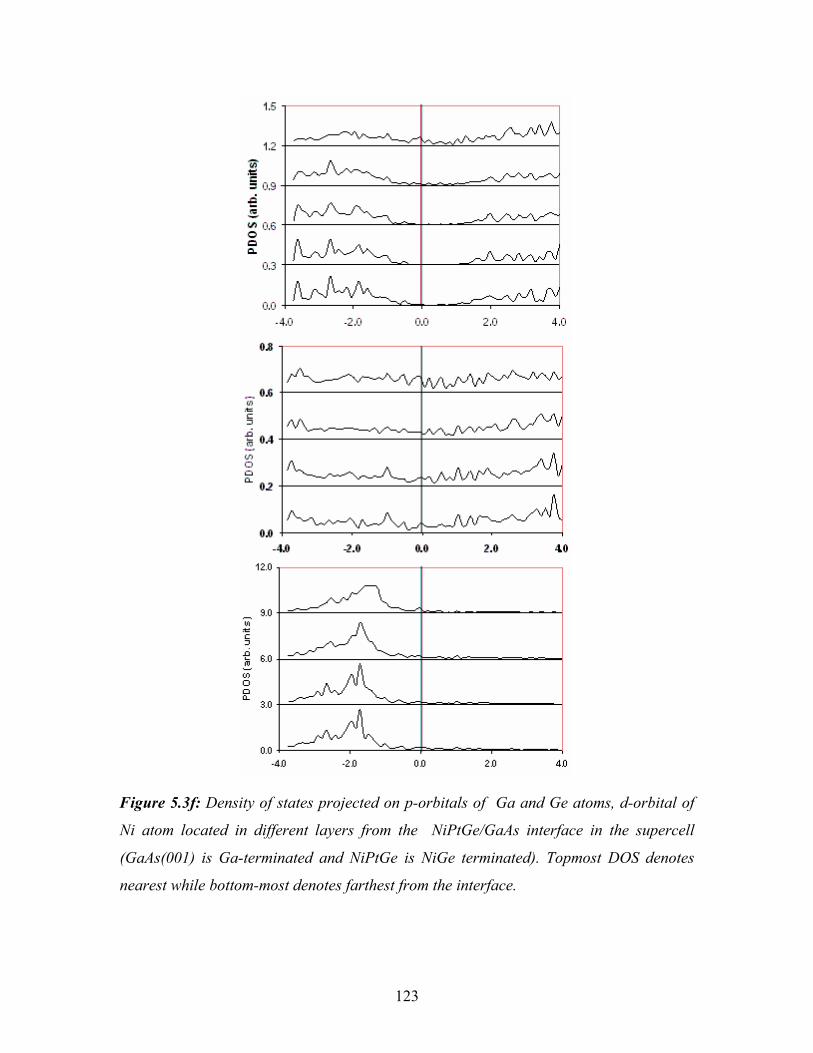
123
Figure 5.3f: Density of states projected on p-orbitals of Ga and Ge atoms, d-orbital of
Ni atom located in different layers from the NiPtGe/GaAs interface in the supercell
(GaAs(001) is Ga-terminated and NiPtGe is NiGe terminated). Topmost DOS denotes
nearest while bottom-most denotes farthest from the interface.

124
Figure 5.3g: Density of states projected on p-orbitals of As and Ge atoms, d-orbital of Pt
atom located in different layers from the NiPtGe/GaAs interface in the supercell
(GaAs(001) is As-terminated and NiPtGe is PtGe terminated). Topmost DOS denotes
nearest while bottom-most denotes farthest from the interface.

125
Chapter 6
Magnetic state of β-MnAs
α-MnAs (Fig. 6a) was studied 100 years ago [161] and found to be ferromagnetic
seven years later [162]. There has been recent renewed interest in MnAs because of its
possible spintronic applications. Ramsteiner et al. [163] have studied spin injection from
MnAs layers into GaAs while Tanaka et al. [164, 165] have measured the epitaxial
orientation and magnetic properties of MnAs thin films grown on GaAs. Although we
know of no calculations of β-MnAs, there are three calculations [166-168] of the
properties of zinc-blende MnAs, a phase which has never been grown and which was
shown [7] could not be stabilized either by lattice stretching or compression. More
interesting to us is the β phase (Fig 6a), which is not ferromagnetic and which experiment
has suggested is neither paramagnetic nor antiferromagnetic. The transition from the
hexagonal NiAs (space-group number 194) a phase to the orthorhombic MnP (space-
group number 62) β phase is first order and occurs at 40 °C (Ref. 169) or 44 °C (Ref.
170), the difference probably resulting from slightly different sample stoichiometries.
Extrapolation of the magnetization versus temperature curve gives a Curie temperature
[171] for the α phase of about 127 °C. The resistivity of the β phase at 100 °C is about 3.3
times that of a phase at 35 °C [172, 173]]. Ney et al. [174] have found that the α and β
phases coexist between 10 and 40 °C in heteroepitaxially constrained MnAs/ GaAs(001)
films. The fact that β-NiAs transforms to the paramagnetic γ phase (with the same NiAs
structure as the α phase) at 130 °C, essentially the extrapolated Curie temperature of the a
phase, together with the anomalous behavior of the inverse susceptibility of the β phase,
led Guillaud [173] to speculate that β-MnAs is antiferromagnetic. However, no long-
range magnetic order has been detected by neutron diffraction [169, 175]. Unlike β-
MnAs, γ-MnAs shows normal Curie-Weiss behavior [173]. There have been three
different explanations for the α to β transition. Kittel [176] proposed two ferromagnetic

126
sublattices whose exchange coupling changed sign at the transition temperature leading
to a ferromagnetic-antiferromagnetic transition. This theory was rejected by Goodenough
and Kafalas [171] because no antiferromagnetic order had been observed. Rodbel et al.
[177, 178] purported to show with theory and experiment that the transition was
ferromagnetic to paramagnetic. Their theory showed how such a phase transition could
be first order in a very compressible material with a strongly volume-dependent exchange
interaction. The α → β transition with increasing pressure has been measured by others
[171] as has the β to α transition with increasing magnetic field [170, 179]. Goodenough
[171, 180] pointed out how the α to β and β to γ transition could be explained by a high
spin Mn configuration in the α and γ phases and a low spin Mn configuration in the β
phase. Andresen et al. [181] found a spiral density wave in β-MnAs. They worked at 4.2
and 80 K without stating whether it was present at both temperatures. The β phase,
created with 12.6 kbar of pressure, remains metastable below 160 K at 1 bar. The β phase
can also be stabilized by substituting a small amount of V, Cr, Fe, Co, or Ni for the Mn,
or P for the As, resulting in a Néel temperature of 200-230 K. Thus, it is unlikely
(especially since it has never been observed) that β-MnAs above 40 °C would support a
spiral spin-density wave. We now restate the facts concerning the β phase and then give
the only description of the β phase consistent with these facts and with Occam’s razor. β-
MnAs is not ferromagnetic. It is unlikely to be paramagnetic because it does not have
Curie or Curie-Weiss behavior. Unlike the α to β transition, Jahn-Teller structurally
driven phase transitions go from lower to higher symmetry with increasing temperature.
Thus, except for the fact that no antiferromagnetic order has been seen in the β phase, this
transition would seem to be magnetically driven, from the high symmetry ferromagnetic
state to a lower symmetry antiferromagnetic state. Our solution to this conundrum is that
β-MnAs consists of antiferromagnetic planes of Mn but that the exchange coupling
between planes is so weak that the ordering of the planes is random, i.e., an up spin in
one plane is equally likely to be below an up or a down spin in the plane above. This
randomness accounts for the failure of neutron scattering to detect long-range
antiferromagnetic order. In the next section we show that this description is consistent
with the results of density functional calculations.

127
Figure 6a: (a) α-MnAs (B81) unit cell containing two Mn and two As atoms, (b) β-MnAs
(B31) unit cell containing four Mn and four As atoms.
6.1 Calculations and results
These ultrasoft pseudopotential [85] calculations were done using the PWSCF
package of Baroni et al. [182]. We sampled a 12×12×8 k-point mesh in the hexagonal
Brillouin zone (cf. 3×3×3 in Ref. 167) and a 12×8×8 in the orthorhombic. The PBE (Ref.
100) exchange-correlation density functional was used and plane waves up to 35 Ry were
used in the expansion. The partial core correction [183] was used on the As atoms, but, in
lieu of one on Mn, the Mn 3s and 3p semicore states were included in the calculations.
The hexagonal calculations were converged to 10-8 Ry while the orthorhombic
calculations were converged to 10-5 Ry. The orthorhombic lattice constants and atomic
displacements were calculated starting from the experimental values and iterating until all
forces were less than 0.4 mRy/bohr and all stresses less than 0.22 mRy/bohr3. A plot of
minus the cohesive energy (obtained by subtracting the energy of spin-polarized atoms
from the total energy) and the magnetization of α-MnAs versus volume is displayed in

128
Fig. 6.1a. One sees that it requires about a 47% reduction in the volume from its
equilibrium value to cause the magnetization to disappear in what appears to be a second-
order phase transition.
Figure 6.1a: Magnetization of a-MnAs in bohr magnetons per MnAs (solid line) and
negative of the cohesive energy per MnAs in eV (dashed line) as a function of volume.
Although there would be a transition to the β phase before this occurred, the volume
dependent magnetization theory of Rodbell et al. [177, 178] does not require a structural
transition. Because the β-phase volume is only 2% smaller [169] than the α, it is highly
unlikely that the theory of Rodbell et al. is applicable to the phase transition in MnAs. In
Table 6.1a, we compare the equilibrium volume, cohesive energy, c/a ratio, bulk
modulus, and magnetization with experiment for α-MnAs. The volume and c/a were
measured [181] at 4.2 K. Our 0.96% discrepancy with the experimental volume is
extremely small for a density functional calculation while our c/a ratio is no better than
fair agreement with experiment. The c/a ratio decreased monotonically with volume from
1.76 at V=254.5 bohr3 to 1.39 at V=649.0 bohr3. Because of the nonlinearity of the
exchange-correlation potential, our excellent agreement with the experimental [171]

129
magnetization might have been slightly worse had more core electrons been included in
the calculation. Our zero-temperature bulk modulus seems not inconsistent with the 273-
K experimental [184] value. We could find no experimental value for the cohesive
energy, but our calculated cohesive energy is quite consistent with our bulk modulus. For
example, scandium has a bulk modulus of 43.5 GPa (Ref. 132) and a cohesive energy of
7.8 eV (Ref. 132) per two atoms. Figure 6.1b is a plot of the spin density of states (DOS)
at the calculated equilibrium volume. The split off low energy states are the As 4s bands
while the higher lying states come from the hybridizing As 4p and Mn 3d bands.
Vol Ecoh c/a M B
Calc. 456.21 6.982 1.488 3.32 44.5
Expt. 460.62a 1.519a 3.4b 35.8c
TABLE 6.1a: Equilibrium unit-cell volume (in bohr3), cohesive energy (in eV per MnAs),
c/a ratio, magnetization (in bohr magnetons per Mn atom), and bulk modulus (in GPa)
compared with experiment for α-MnAs. Superscripts a, b and c refers to References
[181], [171] and [184] respectively.

130
Figure 6.1b: Majority (solid line) and minority spin (dashed line) densities of states in
electrons per eV per unit cell of α-MnAs. The Fermi energy is at E=0.
The β-MnAs unit cell is obtained from the α by small distortions as follows. A hexagonal
lattice has a centered rectangular unit cell with ab 3 and twice the area. b and a each
relax by about -1%, almost, but not quite, maintaining their 31/2 ratio, while c does not
relax at all [169]. Although the unit cell is almost hexagonal, there are sizable inner
displacements of the atoms which destroy the almost hexagonal symmetry. We have
defined a, b, and c to be consistent with the hexagonal lattice. To get the standard
definition used in Ref. [169] (abc)→(bca).
In Table 6.1b we list the cohesive energy and magnetization for ferromagnetic,
paramagnetic, and three different antiferromagnetic structures of β-MnAs (Fig 6.1c). The
two (001) planes of Mn are ferromagnetic but oppositely polarized in AFI. In AFII the
planes are antiferromagnetic with up (down) spins in one plane below up (down) spins in
the other, and in AFIII the down (up) spins are below the up (down). The results are
listed for the fully relaxed positions as well as for the starting high-temperature [169]
lattice constants and inner displacements which are listed in Tables 6.1c and 6.1d. It is
interesting to note that with the experimental lattice parameters the ferromagnetic state is
still the ground state. It relaxes back to α-MnAs. It is also interesting to note that in spite
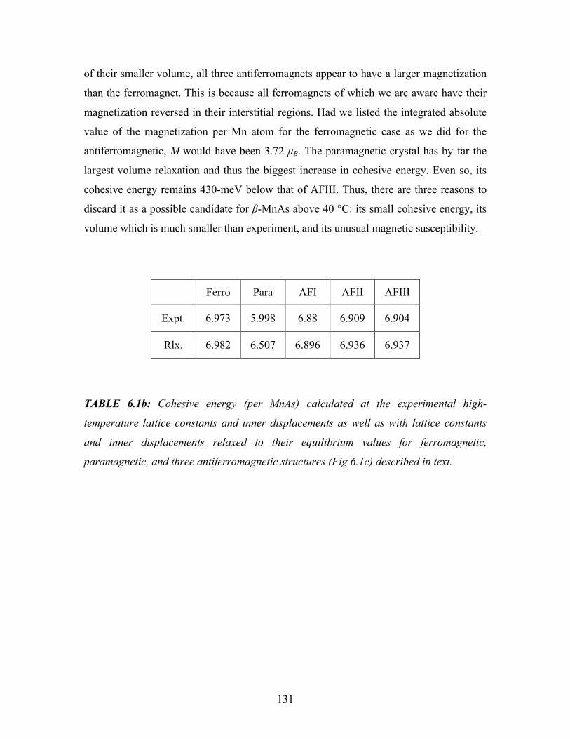
131
of their smaller volume, all three antiferromagnets appear to have a larger magnetization
than the ferromagnet. This is because all ferromagnets of which we are aware have their
magnetization reversed in their interstitial regions. Had we listed the integrated absolute
value of the magnetization per Mn atom for the ferromagnetic case as we did for the
antiferromagnetic, M would have been 3.72 μB. The paramagnetic crystal has by far the
largest volume relaxation and thus the biggest increase in cohesive energy. Even so, its
cohesive energy remains 430-meV below that of AFIII. Thus, there are three reasons to
discard it as a possible candidate for β-MnAs above 40 °C: its small cohesive energy, its
volume which is much smaller than experiment, and its unusual magnetic susceptibility.
Ferro Para AFI AFII AFIII
Expt. 6.973 5.998 6.88 6.909 6.904
Rlx. 6.982 6.507 6.896 6.936 6.937
TABLE 6.1b: Cohesive energy (per MnAs) calculated at the experimental high-
temperature lattice constants and inner displacements as well as with lattice constants
and inner displacements relaxed to their equilibrium values for ferromagnetic,
paramagnetic, and three antiferromagnetic structures (Fig 6.1c) described in text.

132
Figure 6.1c: Antiferromagnetic models of β-MnAs used for calculations.
Figure 6.1d: Total density of states in electrons per eV per unit cell of β-MnAs. The
Fermi energy is at E=0.
In Table 6.1c we note that the relaxed lattice constants of all three
antiferromagnetic structures are smaller than the experimental values at 55 °C, as
expected, but that they are larger than those measured at 4.2 K under 12.6 kbar of applied
pressure while the paramagnetic lattice constants are much smaller than the experimental

133
ones under 12.6 kbar. Table 6.1d displays the displacements of the atoms in the
orthorhombic structure away from their positions in the hexagonal structure. One
peculiarity is that the atomic displacements of AFI away from hexagonal are much
smaller than those of AFII and AFIII but its b/a=1.745 is much further from the
hexagonal 3 than the 1.731 of both AFII and AFIII. Figure 6.1d is the DOS of AFIII. If
we divide these in half (because the unit cell is twice as large) and compare them with the
sum of spin DOS of Fig. 6.1b, we see that at the Fermi energy the β-phase DOS is about
8% larger than the α. Thus, the 3.3 times larger resistivity of the β phase [172, 173] must
be due to other sources, such as the 65-K higher temperature at which it was measured, in
addition to the postulated disorder of its antiferromagnetic planes.
.
a b c V M
Ferro. 7.070 12.246 10.522 910.99 3.32
Para. 6.405 11.427 10.215 747.69 0.00
AFI 6.830 11.915 10.768 876.29 3.38
AFII 6.879 11.907 10.732 878.98 3.56
AFIII 6.866 11.888 10.716 874.73 3.40
55°Ca 6.931 12.032 10.809 901.40
4.2Kb 6.603 11.641 10.547 810.70
TABLE 6.1c: Calculated orthorhombic lattice constants (in bohr), volume (in bohr3),
and magnetization (in bohr magnetons per MnAs) for the five crystals in Table 6.1b,
compared with experimental values at 55 °C and 4.2 K with an applied pressure of 12.6
kbar. Note that b= 31/2 a for the ferromagnetic case which has hexagonal symmetry.
Superscript a and b refers to references [169] and [181] respectively.

134
α β γ δ
Ferro. 0 0 0 0
Para. 0.0528 0.0056 0.0069 0.0539
AFI 0.0100 0.0014 0.0001 0.0082
AFII 0.0475 0.0135 0.0049 0.0447
AFIII 0.0435 0.0030 20.0019 0.0444
Expa 0.0271 0.0047 0.0020 0.0245
TABLE 6.1d: Calculated positions of the atoms within the unit cells of Table 6.1c
compared with experiment at 55 °C. The Mn atoms are at [1/4, ¼ - α, -β], [3/4, 3/4 + α,
+β], [3/4, 3/4 - α, ½ +β], [1/4, ¼ + α, ½ -β] and the As atoms are at [1/4, -1/12 + γ, ¼ +
δ], [3/4, 1/12 - γ, 3/4 + δ], [3/4, 5/12 + γ, ¼ - δ], [1/4, 7/12 - γ, 3/4 + δ]. Superscript ‘a’
refers to reference [169].
6.2 Conclusion
We believe that our calculation is sufficiently accurate to discard the possibility of
β-MnAs being paramagnetic even without considering its non-Curie-Weiss magnetic
susceptibility. Since it is not ferromagnetic, that leaves only the possibility of its being a
planar antiferromagnet with planes randomly ordered to account for the lack of observed
antiferromagnetic order or its being in some more complicated state that we have not
considered. A spin glass seems highly unlikely for an ordered compound and a spin-
density wave or spiral spin-density wave would have been detected by neutron scattering.
The question then remains, how consistent is this random antiferromagnetic state with
our calculations? We see that AFIII (aligned planes) and AFII (staggered planes) are
degenerate, which makes it very likely that their free energies at 40 °C will be very close
to degenerate and that rather than be staggered or aligned, the planes will be random. We
found the random antiferromagnet state lies 40 meV below AFI with its alternating
ferromagnetic planes. It also lies 45 meV above the hexagonal ferromagnetic state. The

135
fact that the α → β transition occurs with increasing temperature indicates that there are
contributions to the entropy which favor the antiferromagnetic β phase over the
ferromagnetic α phase. We can only speculate what these might be. The almost perfect
hexagonal lattice symmetry indicates that the inner displacements of Table 6.1d select 1
of 6 equivalent sets of atomic sites. If some of the energy barriers between these sites are
small, they could cause there to be very low-frequency phonon modes in the β phase
which are not present in the α phase [185]. These, together with the uncertainities of
density functional theory, should be sufficient to account for the 45 meV in the free
energy needed to account for the transition to the disordered antiferromagnetic state.
Therefore, we believe that our proposed disordered antiferromagnetic state is consistent
with these calculations and is the most likely state for β-MnAs.

136
REFERENCES
[1] S. Zhang and M. Ostling, Crit. Rev. in Solid State and Mat. Sci. 28, 1 (2003)
[2] C. Detavernier, A.S. Özcan, J. Jordan-Sweet, E.A. Stach, J. Tersoff, F.M. Ross and C.
Lavoie, Nature 426, 641 (2003).
[3] C. Detavernier and C. Lavoie, Appl. Phys. Lett. 84, 3549 (2004).
[4] J. Iwai, T. Ohguro, and S. Ohmi, Microel. Eng. 60, 157 (2002).
[5] S. R. Murarka, Metallization: Theory and practice for VLSI application (Butterworth-
Heinemann, Boston, 1993).
[6] S. R. Murarka, Silicides for VLSI Applications (Academic, New York, 1983)
[7] C. Blair, E. Demirlioglu, E. Yoon, and J. Pierce, Silicides, Germanides and their
interfaces, edited by R. W. Fathauer, L. Schowalter, S. Mantl, and N. K. Tu, MRS
Symposia Proceedings No. 320 (Materials Research Society, Pittusberg, 1994).
[8] W. J. Taylor, M. J. Rendon, E. Verret, J. Jiang, C. Capasso, D. Sing, J. Y. Nguyen, J.
Smith, E. Luckowski, A. Martinez, J. Schaeffer, Phil Tobin, Mat. Res. Soc. Symp. Proc.
Vol. 810 (2004).
[9] C. Detavernier, C. Lavoie, R.L. Van Meirhaegh e, Thin. Solid Films 468, 174 (2004)
[10] R.N. Wang and J.Y. Feng, J. Phys.: Condens. Matter 15, 1935 (2003).
[11] M. Liehr, P.E. Schmid, F.K. Le Gouse, and P.S. Ho, Phys. Rev. Lett. 54, 2139
(1985).
[12] D. –X. Xu, S. R. Das, L. Erickson, and A. Naem, Materials Reliability in
Microelectronics V, edited by A. S. Oates, W. F. Filter, R. Rosenberg, A. L. Greer, and
K. Gadepally, MRS Symposia Proceedings No. 391 (Materials Research Society,
Pittsburgh, 1995), p. 223
[13] D. –X. Xu, J. P. McCaffrey, S. R. Das, G. C. Aers, and L. E. Erickson, Appl. Phys.
Lett. 68, 3588 (1996).
[14] M. L. Lee, E. A. Fitzgerald, M. T. Bulsara, M. T. Currie, and A. Lochtefeld, J.
Appl. Phys. 97, 011101 (2005).
[15] H. Shang, H. Okorn-Schimdt, J. Ott, P. Kozlowski, S. Steen, E. C. Jones, H. –S.P
Wong and W. Hanesch, IEEE Electron Device Lett., 24 , 242 (2003).

137
[16] H. Shang, K. -L Lee, P. Kozlowski, C. D'Emic, I. Babich, E. Sikorski, I. Meikei,
H. –S. P. Wong, K. Guarini and W. Haensch, IEEE Electron Device Lett., 25 , 135
(2004).
[17] A. Ritenour, A. Khakifirooz, D. A. Antoniadis, R. Z. Lei, W. Tsai, A. Dimoulas, G.
Mavrou, and Y. Panayiotatos, Appl. Phys. Lett. 88, 132107 (2006).
[18] N. Wu, Q. Zhang, C. Zhu; D. S. H Chan, A. Du, N. Balasubramanian, M. F. Li, A.
Chin, J. K. O. Sin, D. –L. Kwong, IEEE Electron Device Lett. 25, 631 (2004).
[19] J. Bardeen and W.H. Brattain, Phys. Rev. 74, 230 (1948).
[20] G.D. Wilk and R.M. Wallace, and J.M. Anthony, J. Appl. Phys. 89, 5243 (2001).
[21] Huang et. al, Tech. Dig. Int. Electron Devices Meet., 13.4.1 (2003).
[22] S. Zhu, L. Rui, S. J. Lee, M. F. Li, A. Du, J. Singh, C. Zhu; A. Chin, D. L. Kwong,
IEEE Electron Device Lett., 26 , 81 (2005).
[23] D. Z. Chi, R. T. P. Lee, S. J. Chua, S. J. Lee, S. Ashok, and D.-L. Kwong, J. Appl.
Phys. 97, 113706 (2005).
[24] Int. Technol. Roadmap for Semiconductors, 2005 Edition [http://public.itrs.net]
(SEMATECH, 2005)
[25] S. Datta, T. Ashley, J. Brask, L. Buckle, M. Doczy, M. Emeny, D. Hayes, K. Hilton,
R. Jefferies, T. Martin, T. Philips, D. Wallis, P. Wilding, R. Chau, IEDM Tech. Dig.
2005, 34.1-34.4.
[26] S. Datta, Microelec. Engineering, 84, 2133 (2007)
[27] R. Droopad, K. Rajagopalan, J. Abrokwah, P. Zurcher, M. Passlack, Microelec.
Engineering, 84, 2138 (2007)
[28] M. Murakami and Yasuo Koide, Crit. Rev. in Solid State and Mat. Sci. 23, 1 (1998).
[29] Y. Taur and T. H. Ning , Fundamentals of modern VLSI devices, Cambridge
University Press (1998).
[30] K. K. Ng and W. T. Lynch, IEEE Trans. Electron Devices ED-34, 503 (1987).
[31] K. A. Jenkins, J. N. Burghartz, and P. D. Agnello, IEEE Trans. Electron Devices
ED-43, 759 (1996).
[32] W. Monch, Electronic structure of metal-semiconductor contacts (Kluwer,
Dordrecht, 1990).
[33] R. T. Tung, Materials Science & Engineering R-Reports, 35(1-3), 1 (2001).

138
[34] Crowell, C. R. and Rideout, V. L., Solid State Electron., 12, 89, 1969.
[35] Stratton, R. and Padovani F. A., Solid State Electron., 10, 813, 1967.
[36] Robinson, G. Y., in Physics and Chemistry of III-V Compound Semiconductor
Interfaces, Wilmsen, C. W., Ed., Plenum Press, New York, 1985, 195.
[37] Sze, S. M., Physics of Semiconductor Devices, Wiley, New York, 1981, 245.
[38] G. Margaritondo. Electronic structure of semiconductor heterojunctions (Kluwer,
Dordrecht, 1988).
[39] G. Margaritondo. Reports on Progress in Physics, 62(5), 765 (1999).
[40] L. J. Brillson. Contacts to semiconductors fundamentals and technology (Noyes
Publications, Park Ridge, New Jersey, 1993).
[41] E. H. Rhoderick and R. H. Williams. Metal-semiconductor contacts (Clarendon
Press, Oxford, 1988), 2nd edition.
[42] E. G. Clarke and A. W. Czanderna, Surface Science, 49(2), 529 (1975).
[43] L. J. Brillson., Applied Surface Science, 11-2(JUL), 249 (1982).
[44] A. Zangwill and A. C. Redfield, Journal of Physics F-Metal Physics, 18(1), 1 (1988).
[45] F. Braun. Ueber die Stromleitung durch Schwefelmetalle. Annalen der Physik und
Chemie, 153, 556 (1874).
[46] W. Schottky and W. Deutschmann. Zum Mechanismus der Richtwirkung von
Kupfergleichrichtern. Physikalische Zeitschrift, 30, 839 (1929).
[47] E. H. Rhoderick, Journal of Physics D-Applied Physics, 5(10), 1920 (1972).
[48] A. G. Milnes and D. L. Feucht. Heterojunctions and metal-semiconductor junctions
(Academic Press, New York, 1972).
[49] F. Capasso and G. Margaritondo (editors). Heterojunction band discontinuities
physics and device applications (North-Holland, Amsterdam, 1987).
[50] E. H. Rhoderick, Journal of Applied Physics, 46(6), 2809 (1975).
[51] H. Kroemer, Surface Science, 132(1-3), 543 (1983).
[52] N. Newman, M. Vanschilfgaarde, T. Kendelwicz, M. D. Williams, and W. E. Spicer,
Physical Review B, 33 (2), 1146 (1986).
[53] J. R. Waldrop, Journal of Vacuum Science & Technology B, 2(3), 445 (1984).
[54] M. Prietsch. Ballistic-Electron-Emission Microscopy (BEEM) - Studies of Metal-
Semiconductor Interfaces with Nanometer Resolution. Physics Reports-Review Section

139
of Physics Letters, 253(4), 164 (1995).
[55] W. J. Kaiser and L. D. Bell, Physical Review Letters, 60 (14), 1406 (1988).
[56] L. D. Bell, W. J. Kaiser, M. H. Hecht, and F. J. Grunthaner, Physics Letters, 52 (4),
278 (1988).
[57] L. J. Brillson. Surfaces and Interfaces: Atomic-Scale Structure, Band Bendeing and
Band Offsets. In Handbook on semiconductors (edited by T. S. Moss), volume 1, pages
281–417 (North-Holland, Amsterdam, 1992)
[58] W. Schottky. Halbleitertheorie der Sperrschicht. Naturwissenschaften, 26(52), 843
(1938).
[59] N. F. Mott, Proceedings of the Cambridge Philosophical Society, 34, 568 (1938).
[60] S. Kurtin, T. C. Mcgill, and C. A. Mead, Physical Review Letters, 22(26), 1433
(1969).
[61] M. Schl¨uter, Physical Review B, 17 (12), 5044 (1978).
[62] M. Murakami and Y. Koide, Critical reviews in Solid state and material sciences,
23(1), (1998)
[63] J. Bardeen, Physical Review, 71, 717 (1947).
[64] I. Y. Tamm. ¨ Uber eine m¨ogliche Art der Elektronenbindung an
Kristalloberfl¨achen. Physikalische Zeitschrift der Sowjetunionen, 1, 733 (1932).
[65] W. Shockley, Physical Review, 56, 317323 (1939).
[66] A. M. Cowley and S. M. Sze, Journal of Applied Physics, 36(10), 3212 (1965).
[67] V. Heine, Physical Review, 138(6A), 1689 (1965).
[68] W. E. Spicer, P. W. Chye, P. R. Skeath, C. Y. Su, and I. Lindau, Journal of Vacuum
Science & Technology, 16(5), 1422 (1979).
[69] H. Hasegawa and H. Ohno, Journal of Vacuum Science & Technology B, 4 (4),
1130 (1986).
[70] R. T. Tung, Physical Review Letters, 84 (26), 6078 (2000).
[71] J. Tersoff, Physical Review Letters, 52 (6), 465 (1984).
[72] J. J. Rehr and W. Kohn, Phys. Rev. B 9, 1981 (1974)
[73] H. H. Wieder, Journal of Vacuum Science & Technology, 15 (4), 1498 (1978).
[74] W. Monch, J. Vac. Sci. Technol. B 17, 1867 (1999)
[75] R. T. Tung, Phys. Rev. Lett. 52, 461 (1984)

140
[76] R. G. Dandrea and C. B. Duke, J. Vac. Sci. Technol. B 11, 1553 (1993)
[77] J. L. Freeouf, Appl. Phys. Lett. 41, 285 (1982).
[78] R. T. Tung, J. Vac. Sci. Technol. B 11, 1546 (1993).
[79] R. P. Iczkowsky and J. L. Margrave, J. Am. Chem. Soc. 83, 3547 (1961).
[80] A. K. Rappe and W. A. Goddard III, J. Phys. Chem. 95, 3358 (1991).
[81] R. Winkler and S. T. Pantelides, J. Chem. Phys. 106, 7714 (1997).
[82] M. Schlüter, Phys. Rev. B 17, 5044 (1978)
[83] P. Hohenberg, and W. Kohn, Phys. Rev. 136, B864 (1964).
[84] W. Kohn, and L. J. Sham, Phys. Rev. 140, A1133 (1965).
[85] D. Vanderbilt, Physical Review B, 41(11), 7892 (1990).
[86] P. E. Blöchl, Phys. Rev. B 50, 17953 (1994).
[87] E. K. U. Gross and R. M. Dreizler. Density functional theory an approach to the
quantum many-body problem (Springer, Berlin, 1990).
[88] W. Kohn. Highlights of Condensed-Matter Theory. In International School of
Physics ”Enrico Fermi” (edited by F. Bassani, F. Fumi, and P. Tosi), pages 1–15
(North-Holland, Amsterdam, Varenna on Lake Como, Villa Monastero, 28 June -
16 July 1983, 1985).
[89] R. G. Parr andW. Yang. Density-functional theory of atoms and molecules (Oxford
University Press, New York, 1989).
[90] R. O. Jones and O. Gunnarsson, Reviews of Modern Physics, 61(3), 689 (1989).
[91] W. E. Pickett, Computer Physics Reports, 9(3), 115 (1989).
[92] R. M. Martin, Electronic Structure (Cambridge University Press, Cambridge, 2003)
[93] M. Born and J. R. Oppenheimer, “Zur Quantentheorie der Molekeln”, Ann. Physik
84:457, 1927
[94] H. Hellmann. Einf¨uhrung in die Quantenchemie (Deuticke, Leipzig, 1937)
[95] R. P. Feynman, Physical Review, 56, 340 (1939).
[96] W. Kohn and L. J. Sham, Physical Review, 137, A1697 (1965).
[97] D. M. Ceperley and B. J. Alder, Physical Review Letters, 45(7), 566 (1980).
[98] J. P. Perdew and A. Zunger, Physical Review B, 23, 5048 (1981).
[99] J. P. Perdew and Y. Wang, Phys. Rev. B, 45, 13244 (1992)
[100] J. P. Perdew, K.Burke, and M. Ernzerhoff, Phys. Rev. Lett. 77, 3865 (1996).

141
[101] B. Holm and U. von Barth, Physical Review B, 57(4), 2108 (1998).
[102 B. Holm, Physical Review Letters, 83(4), 788 (1999).
[103] N. W. Ashcroft and N. D. Mermin. Solid state physics (Saunders College,
Philadelphia, 1976).
[104] J. Ihm, A. Zunger, and M. L. Cohen, Journal of Physics C-Solid State Physics,
12(21), 4409 (1979).
[105] O. H. Nielsen and R. M. Martin, Physical Review B, 32(6), 3792 (1985).
[106] O. H. Nielsen and R. M. Martin, Physical Review B, 32(6), 3780 (1985).
[107] J. C. Phillips and L. Kleinman, Phys. Rev., 116, 287 (1959)
[108] W. E. Pickett, Computer Physics Reports, 9(3), 115 (1989).
[109] D. R. Hamann, M. Schl¨uter, and C. Chiang, Physical Review Letters, 43, 1494
(1979).
[110] G. B. Bachelet, D. R. Hamann, and M. Schl¨uter, Physical Review B, 26(8), 4199
(1982).
[111] D. Vanderbilt, Physical Review B, 41(11), 7892 (1990).
[112] N. Troullier and J. L. Martins, Physical Review B, 43(3), 1993 (1991).
[113] L. Kleinman and D. M. Bylander, Physical Review Letters, 48(20), 1425 (1982).
[114] X. Gonze, P. Kackell, and M. Scheffler, Physical Review B, 41(17), 12264 (1990).
[115] X. Gonze, R. Stumpf, and M. Scheffler, Physical Review B, 44(16), 8503 (1991).
[116] P. E. Blöchl, Phys. Rev. B 50, 17953 (1994).
[117] A. Baldereschi, Physical Review B, 7(12), 5212 (1973).
[118] H. J. Monkhorst and J. D. Pack, Physical Review B, 13(12), 5188 (1976).
[119] G. Gilat, J. Comput. Phys. 10, 432-65, 1972
[120] A. H. MacDonald, S. H. Vosko, and P. T. Coleridge, J. Phys. C: Solid State Phys.
12:2291-3002, 1979
[121] P. E. Blochl, O. Jepsen, and O. K. Andersen, Phys. Rev. B 49, 16223-16233, 1994.
[122] L. Kleinman, Physical Review B, 24(12), 7412 (1981)
[123] S. Baroni, R. Resta, A. Baldereschi and M. Peressi, in: Spectroscopy of
Semiconductor Microstructures, Eds. G. Fasol, A. Fasolino and P. Lugli (Plenum,
London, 1989) p. 251.

142
[124] C. G. Van de Walle, R. M. Martin, Phys. Rev. B 34 5621 (1986); C. G. Van de
Walle, R. M. Martin, Phys. Rev. B 35 8154 (1987);
[125] S. Massidda, B.I. Min and A.J. Freeman, Phys. Rev. B 35 (1987) 9871.
[126] Zhu, X. and S.G. Louie, Phys. Rev. B 43, 14142 (1991)
[127] Bylander, D.M. and L. Kleinman, Phys. Rev. Lett. 60, 472 (1988)
[128] A. Baldereschi, S. Baroni and R. Resta, Phys. Rev. Lett. 61, 734 (1988).
[129] G. X. Qian, R. M. Martin and D. J. Chadi, Phys. Rev. B, 38, 7649 (1992)
[130] F. Reif, Fundamentals of statistical and Thermal Physics (McGraw-Hill, New
York, 1965)
[131] J. F. Nye, Physical Properties of Crystals (Oxford University Press, Oxford, 1985)
[132] D. C. Wallace, Thermodynamics of Crystals (Wiley, New York, 1972).
[128] H. Pfisterer and K. Schubert, Z. Metallkd. 41, 358 (1950).
[129] E. J. Graeber, R. J. Baughman, and B. Morossin, Acta Cryst. B 29, 1991 (1973).
[130] N. Franco, J. E. Klepeis, C. Bostedt, T. Van Buuren, C. Heske, O. Pankratov, T. A.
Callcott, D. L. Ederer, and L. J. Terminello, Phys. Rev. B 68, 045116 (2003).
[131] O. Beckstein, J. E. Klepeis, G. L. W. Hart, and O. Pankratov, Phys. Rev. B 63,
134112 (2001).
[132] C. Kittel, Introduction to Solid State Physics, 6th ed. (Wiley, New York, 1986).
[133] E. J. Graeber, R. J. Baughman, and B. Morossin, Acta. Cryst. B 29, 1991 (1973).
[134] G. Kresse, and J. Furtmuller, Phys. Rev. B 54, 11169 (1996).
[135] I. G. Batyrev, L. Kleinman and J. Leiro, Phys. Rev. B 70, 073310 (2004).
[136] J. Padilla and D. Vanderbilt, Surf. Sci. 418, 64 (1998).
[137] A. A. Naem, J. Appl. Phys. 64, 4161 (1988).
[138] A. K. Pant, S. P. Murarka, C. Shepard and W. Lanford, J. Appl. Phys. 72, 1833
(1992).
[139] C. Chang, B. Cunningham, A. Segmüller, H. C. W. Huang, F. E. Turene, A.
Sugerman, and P. A. Totta, J. Vac. Sci. Technol. B 4, 745 (1986).
[140] X. Zhang, A.A. Demkov, H. Li, X. Hu, Y. Wei, J. Kulik, Phys. Rev. B 68, 125323
(2003).
[141] M. Kiskinova, G. Pirug and H. P. Bonzel, Surf. Sci. 133, 321 (1983).
[142] R. Smoluchowski, Phys. Rev. 60, 661 (1941).

143
[143] S. Adachi, “Properties of group –IV, III-V and II-VI semiconductors”, (John Wiley
& Sons, Chichester, West Sussex, UK, 2005)
[144] M. Elices and F. Yndurain, J. Phys. C: Solid State Phys. 5, L146 (1972).
[145] C. Detavernier, C. Lavoie, and F. M. d’Heurle, J. Appl. Phys. 93, 2510 (2003).
[146] X. Zhang, A.A. Demkov, H. Li, X. Hu, Y. Wei, J. Kulik, Phys. Rev. B 68, 125323
(2003).
[147] D. M. Bylander and Leonard Kleinman, Phys. Rev. B, 36, 3229 (1987)
[148] V. W. Chin, M. A. Green, and J. W. V. Storey, Solid-State Electron. 36,1107
(1993).
[149] J. Y. Spann, R. A. Anderson, T. J. Thornton, G. Harris, C. Tracy, IEEE Electron
Device Lett., 26, 151 (2005).
[150] E. J. Graber, R. J. Baughman, and B. Morosin, Acta. Crys. B 29, 1991 (1973).
[151] B. Balakrisnan, C. C. Tan, S. L. Liew, P. C. Lim, G. K. L. Goh, Y. L. Foo, and D.
Z. Chi, Appl. Phys. Lett. 87, 241922 (2005).
[152] R. Nath, C. W. Soo, C. B. Boothroyd, M. Yeadon, D. Z. Chi, H. P. Sun, Y. B.
Chen, X. Q. Pan, and Y. L. Foo, Appl. Phys. Lett. 86, 201908 (2005).
[153] J. C. Slater, Symmetry and energy bands in crystals, Dover ed. (Dover, New York,
1972)
[154] P. Ravindran, L. Fast, P. A. Korzhavyi, B. Johansson, J. Wills, and O. Eriksson, J.
Appl. Phys. 84, 4891 (1998).
[155] E. Birch, J. Geophys. 83, 1257 (1978).
[156] MacFarlane et. al. Phys. Lett. 18, 91 (1965).
[157] M. E. Fine, J. App. Phys. 26, 862 (1995).
[158] Low frequency Properties of Dielectric Crystals, Vol. 29a Landolt-Bornstein, New
Series, Group III, edited by D.F. Nelson (Springer, Berlin, 1992).
[159] B. G. Baker, B. B. Johnson and G. L. C. Maire, Surf. Sci. 24, 572 (1971).
[160] F. Flores, A. Munoz and J. C. Duran, Appl. Surf. Science, 41/42, 144 (1989).
[161] F. Heuser, Z. Angew. Chem. 17, 260 (1904).
[162] S. Hilpertand and T. Dieckmann, Ber. Dtsch. Chem. Ges. A 44, 2378 (1911).
[163] M. Ramsteiner, H. Y. Hao, A. Kawaharazuka, H. J. Zhu, M. Kastner, R. Hey, L.
Daweritz, H. T. Grahn, and K. H. Ploog, Phys. Rev. B 66, 081304(R) (2002).

144
[164] M. Tanaka, J. P. Harbison, M. C. Park, T. Shin, and G. M. Rothberg, T. Shin, Appl.
Phys. Lett. 65, 1964 (1994).
[165] M. Tanaka, K. Saito, M. Goto, and T. Nishmaga, J. Magn. Magn. Mater. 198-199,
719 (1999).
[166] T. Ogawa, M. Shirai, N. Suzuki, and I. Kitagawa, J. Magn. Magn. Mater. 196-197,
428 (1999).
[167] Stefano Sanvito and Nicola A. Hill, Phys. Rev. B 62, 15 553 (2000).
[168] Yu-Jun Zhao, W. T. Geng, A. J. Freeman, and B. Delley, Phys. Rev. B 65, 113202
(2002). Note that the α and β phase notation in this paper is not standard.
[169] R. H. Wilson and J. S. Kasper, Acta Crystallogr. 17, 95 (1964).
[170] F. Ishikawa, K. Koyama, K. Watanabe, and H. Wada, Jpn. J. Appl. Phys., Part 2 42,
L918 (2003).
[171] J. B. Goodenough and J. A. Kafalas, Phys. Rev. 157, 389 (1967).
[172] A. Serres, J. Phys. Radium 8, 146 (1947).
[173] C. Guillaud, J. Phys. Radium 12, 223 (1951).
[174] A. Ney, T. Hesjedal, C. Pampuch, A. K. Das, L. Daweritz, R. Koch, K. H. Ploog,
T. Tolinski, J. Lindner, K. Lenz, and K. Baberschke, Phys. Rev. B 69, 081306(R) (2004).
[175] G. E. Bacon and R. Street, Nature (London) 175, 518 (1955).
[176] C. Kittel, Phys. Rev. 120, 335 (1960).
[177] C. P. Bean and D. S. Rodbell, Phys. Rev. 126, 104 (1962).
[178] R. W. De Blois and D. S Rodbell, Phys. Rev. 130, 1347 (1963).
[179] J. Mira, F. Rivadulla, J. Rivas, A. Fondado, T. Guidi, R. Caciuffo, F. Carsughi, P.
G. Radaellil, and J. B. Goodenough, Phys. Rev. Lett. 90, 097203 (2003).
[180] J. B. Goodenough, M.I.T. Lincoln Laboratory, Lexington MA, Technical Report
No. 345, DDC 435758, 1964 (unpublished).
[181] A. F. Andresen, H. Fjellvag, and B. Lebech, J. Magn. Magn. Mater. 43, 158 (1984).
[182] S. Baroni, A. Dal Corso, S. de Gironcoli, and P. Giannozzi, http:// www.pwscf.org
[183] S. G. Louie, S. Froyen, and M. L. Cohen, Phys. Rev. B 26, 1738 (1982).
[184] Handbook of Physical Quantities, edited by Igor. S. Grigoriev and Evgenii Z.
Meilikhov, (CRC Boca Raton, 1997).

145
[185] We know of no experimental or theoretical work to confirm or refute this
speculation. A calculation to compare the phonon spectra of the two phases is possible,
but the purpose of this paper is to determine the magnetic structure of the b-phase and not
to find the cause of the a to b transition.

146
VITA
Manish Kumar Niranjan was born in Lalitpur, U.P, India on July 22, 1977, the
son of Ashok Niranjan and Asha Niranjan. After completing his work at Jawahar
Navodaya Vidyalaya, Lalitpur, U.P, India, in 1995, he entered Indian Institute of
Technology, Kharagpur, India. He received the B.Sc and M.Sc (Integrated M.Sc) from
Indian Institute of Technology, Kharagpur, India, in May 2000. In August 2000 he
entered the Graduate School of The University of Texas.
Permanent Address: Azad Pura, Guru Nanak Market, Lalitpur, U.P, India 284403
This dissertation was typed by the author