Embed Size (px)
Citation preview

Atomic layer deposition of zinc sulfide with Zn(TMHD)2
Andrew Short, Leila Jewell, Sage Doshay, Carena Church, Trevor Keiber, Frank Bridges,Sue Carter, and Glenn Alersa)
Department of Physics, University of California at Santa Cruz, 1156 High Street, Santa Cruz,California 95064
(Received 1 August 2012; accepted 20 November 2012; published 10 December 2012)
The atomic layer deposition (ALD) of ZnS films with Zn(TMHD)2 and in situ generated H2S as
precursors was investigated, over a temperature range of 150–375 �C. ALD behavior was
confirmed by investigation of growth behavior and saturation curves. The properties of the films
were studied with atomic force microscopy, scanning electron microscopy, energy-dispersive x-ray
spectroscopy, ultraviolet–visible–infrared spectroscopy, and extended x-ray absorption fine
structure. The results demonstrate a film that can penetrate a porous matrix, with a local Zn
structure of bulk ZnS, and a band gap between 3.5 and 3.6 eV. The ZnS film was used as a buffer
layer in nanostructured PbS quantum dot solar cell devices. VC 2013 American Vacuum Society.
[http://dx.doi.org/10.1116/1.4769862]
I. INTRODUCTION
Photovoltaics with absorber layers comprised of non-
silicon material continue to be an expanding area of solar
cell research. Often, in these devices, a buffer layer of cad-
mium sulfide (CdS) is used as an n type layer and to prevent
shunting.1 Recently, zinc sulfide (ZnS) has been substituted
for the CdS, as its higher band gap should allow for greater
efficiencies at shorter wavelengths by letting more high-
energy photons through to the absorbing layer. Zinc is also
more abundant than cadmium and is non-toxic. Atomic layer
deposition (ALD) is the preferred method for creating this
window layer, as it is a conformal process that operates at
relatively low (�100 �C) temperatures, allows for deposition
into highly structured substrates, and has a low energy
cost.2,3 Thus, ALD is an ideal method for creating a thin,
highly conformal layer of material at low energy cost, such
as a window layer of ZnS.
Previously, work in this field has focused on efforts with
the precursors diethyl and dimethyl zinc (DEZn and
DMZn).3–7 These precursors have low boiling points (124 �Cfor DEZn and 46 �C for DMZn) and high vapor pressures,
which make them excellent candidates for ALD. However,
they are also pyrophoric and difficult to work with, each hav-
ing a flash point of �18 �C. Therefore, an alternative precur-
sor was considered for ALD of ZnS.
The precursor chosen was bis(2,2,6,6-tetramethyl-3,
5-heptanedionato)zinc (Zn(TMHD)2), because it is a non-
pyrophoric solid precursor used for the chemical vapor depo-
sition of zinc sulfide.8 The objective of this research was to
examine the viability of Zn(TMHD)2 as a precursor for
atomic layer deposition, and to discover the ideal parameters
for such a process.
II. EXPERIMENT
ALD growth of ZnS was performed in a custom-built hot
wall tube furnace reactor. The base pressure of the system
was 20 mTorr. Two precursors can be simultaneously
introduced into the reactor chamber through separate injec-
tors. Nitrogen was used as the carrier and purge gas at a con-
stant flow rate of 40 sccm. Operating pressure was kept
below 2 Torr during pulse and purge cycles.
The precursors used were Zn(TMHD)2 and H2S.
Zn(TMHD)2 is a solid powder at room temperature with a
melting point of 144 �C and a boiling point of 250 �C at
atmospheric pressure. The Zn(TMHD)2 ampule was heated
to 120 �C and all gas lines were heated to above 90 �C. The
H2S was created in situ via a reaction between aluminum
sulfide powder and water, via the chemical reaction
Al2S3þ 3H2O ! Al2O3þ 3H2S. Approximately, 2.5 g of
Al2S3 powder was combined with 30 cc of water for each
deposition. After the reaction was completed, the H2S
ampule was backfilled with N2, resulting in a partial pressure
for H2S of �400 mm Hg, and a total pressure in the ampule
equal to �750 mm Hg. The H2S gas was passed through a
powder desiccant to reduce the residual water content to less
than 1% of the H2S measured with a residual gas analyzer. If
water were present in the hydrogen sulfide, there is a concern
that ZnO might form instead of ZnS. However, the reaction
ZnOþH2S! ZnSþH2O is exothermic with an enthalpy of
�77 kJ/mol.9,10 Therefore, any ZnO that forms would be
converted to ZnS by the hydrogen sulfide.
The substrates used were 1 mm thick, 1 in.2 quartz glass.
The substrates were cleaned via a 30 min sonication in etha-
nol, and then dried with pressurized nitrogen. Resulting film
thicknesses, morphology, and roughness were measured
using an atomic force microscope (AFM) in tapping mode.
Thickness was measured by abrasively removing a portion
of the film and measuring the step height of remaining film.
Stoichiometry was analyzed by energy-dispersive x-ray
(EDX) spectroscopy using ZnS powder as a reference.
Cross-sectional scanning electron microscopy (SEM) images
of the film in a porous TiO2 matrix were taken to observe the
conformal coating of depositions. Structure was analyzed
with extended x-ray absorption fine structure (EXAFS)
measurements, described in detail below. Band gaps were
determined by ultraviolet–visible–infrared spectroscopy
(UV–Vis–IR), as discussed below. Solar cell devices werea)Electronic mail: [email protected]
01A138-1 J. Vac. Sci. Technol. A 31(1), Jan/Feb 2013 0734-2101/2013/31(1)/01A138/5/$30.00 VC 2013 American Vacuum Society 01A138-1

made using the method described elsewhere.11 Quartz sub-
strates with patterned ITO were used with �100 nm of sol–
gel deposited TiO2 and �200 nm of 30 nm TiO2 nanopar-
ticles as the n type contact layer. A 2.5 nm layer of ALD
ZnS was then deposited on top of the porous TiO2 as a buffer
layer. A 945 nm layer of PbS quantum dots was deposited
using a ligand exchange method described elsewhere,11 and
finally a gold contact was deposited by evaporation. These
devices were used to observe the effect of the ZnS as a
buffer layer in a solar cell.
III. RESULTS AND DISCUSSION
A. Growth rate versus pulse times and temperature
ZnS growth rates as a function of precursor dose time and
nitrogen purge time were studied with the substrate at
375 �C, and growth rate versus dose time was also studied at
150 �C. Growth rate was measured by dividing the film
thickness (measured as a step edge by AFM) by the number
of cycles. In Fig. 1, it is observed that longer dose times cor-
respond to increased thickness per cycle at 375 �C indicating
that some precursor decomposition is present at this temper-
ature. However, for the lower temperatures this increase is
proportionally smaller. For example, the percent increase in
growth rate from a 1 s dose time to 10 s at 375 �C is 163%,
while at 150 �C, the percent increase over the same range is
only 50%. A purge time of approximately 25 s was required
to prevent an increased growth rate characteristic of chemi-
cal vapor deposition, which is seen at shorter purge times as
shown in Fig. 2. Therefore, the pulse sequence chosen for
other depositions was a 2 s Zn(TMHD)2 pulse, 25 s purge, 5 s
H2S pulse, and 25 s purge with a background nitrogen flow
rate of 40 sccm. These parameters were used to analyze the
behavior of the ZnS deposition process over the temperature
range of 150–375 �C.
The growth rate was observed to decrease throughout this
temperature range as shown in Fig. 3. This contrasts with
chemical vapor deposition, where the growth rate increases
with temperature, and is indicative of a surface limited ALD
reaction for these films. The decrease in growth rate arises
from surface desorption of the precursors at higher tempera-
tures. The thicknesses of 150 and 375 �C films after 300
cycles were 51 and 15 nm, respectively, measured with an
atomic force microscope, and correspond to growth rates of
1.7 and 0.5 A/cycle. These rates are comparable to those in
literature studies using DEZn and compressed H2S gas. For
example, the growth rate of 0.5 A/cycle at 375 �C measured
in this study is similar to the 0.7 A/cycle growth rate at
300 �C determined by Kim and Yun.4 Also, Platzer-
Bjorkman et al.5 observed a growth rate of 1.38 A/cycle at
120 �C on glass which is comparable to this work’s meas-
ured value of 1.7 A/cycle at 150 �C. Using the ZnS lattice
dimension of 3.13 A for c(111), these growth rates range
from 0.54 monolayers/cycle at 150 �C to 0.16 monolayers/
cycle at 375 �C.
B. Photospectroscopy
Optical characterization of the films was performed with
UV–Vis–IR for determination of the band gap. ZnS is a direct
band gap semiconductor, with a band gap for films and
nanoparticles reported in the literature of 3.5–4.1 eV.12–19
FIG. 1. ZnS growth rate vs Zn(TMHD)2 dose time at 375 and 150 �C, show-
ing that with more precursor time, the growth rate increases, demonstrating
decomposition, which is reduced at the lower temperature.
FIG. 2. Growth rate vs nitrogen purge time at 375 �C. Longer purge times
prevent CVD behavior, which can be seen for purges as long as 15 s.
FIG. 3. Growth rate vs temperature. The decreased growth rate at higher tem-
peratures is the opposite of expected CVD behavior, where film growth
increases with temperature. The observed behavior corresponds to decreased
surface adhesion of the precursors with increased substrate temperature.
01A138-2 Short et al.: Atomic layer deposition of zinc sulfide with Zn(TMHD)2 01A138-2
J. Vac. Sci. Technol. A, Vol. 31, No. 1, Jan/Feb 2013

Most reports remark that for cubic ZnS the band gap is
3.68 eV and for hexagonal ZnS it is 3.74–3.87.20 UV–Vis–IR
was performed on 300 cycle films deposited at temperatures
of 150, 300, and 375 �C, and selected results are shown in
Fig. 4. Tauc plots of (ah�)2 versus h� were used to estimate
the band gap for the films.21 Films at all three temperatures
display a band gap between 3.47 and 3.58 eV, at the low end
of accepted values for cubic ZnS. The lower range may be
due to band broadening from increased disorder in the films.
This disorder could arise from the presence of both cubic and
hexagonal ZnS.22 This conclusion also agrees with a previous
report by Lahtinen et al., using electroreflectance to show that
both cubic and hexagonal phases are present in ALD ZnS
films grown at certain temperatures.23 Studies in the literature
have claimed that the hexagonal phase becomes the dominant
phase in the 400–500 �C range.4,24
C. Composition and structure via EDX and EXAFS
The stoichiometric composition of our films was deter-
mined via EDX measurements. The measured percent
weights of the sulfur and zinc in each sample were converted
to a stoichiometric ratio by comparison with the measured
percent weights of the same elements in a control sample of
pure ZnS powder. As seen in Table I, our films are within
6% of 1:1 stoichiometric ZnS. The EXAFS data were col-
lected at the Stanford Synchrotron Radiation Lightsource
(SSRL) on beamline 4-1 using a Si (220) double monochro-
mator, detuned 50% at 9800 eV to reduce harmonics. The Zn
K-edge data were collected in fluorescence mode with a Ge
multichannel detector at a temperature of 8 K. Slit heights
were approximately 0.5 mm, which give an energy resolution
of �0.9 eV. The data were reduced using standard techni-
ques (RSXAP),25 converted to k-space, and Fourier trans-
formed into r-space. The Fourier transform range for all the
samples is 3.5–10.5 A�1. The Zn K-edge data for a 51 nm
thin film of ZnS deposited at 150 �C, a 20 nm film deposited
at 150 �C, and a 15 nm film deposited at 375 �C were
compared with control samples of bulk ZnS. The first peak
(Zn-S) corresponds to the nearest S neighbors, while the sec-
ond peak (Zn-Zn) corresponds to the next neighbors, Zn. It
is clear from Fig. 5 that the thin film data are very similar to
that for the bulk material; the main difference is a reduced
amplitude, particularly for the second peak. This second
peak reduction is indicative of either increased local disorder
in the film or smaller nanoscale grain sizes in the film. The
first peak for the 51 nm film and bulk ZnS has the same am-
plitude, whereas the other two thin films have a slight reduc-
tion in this peak, indicating more disorder for the nearest
neighbors. For films as thin as these two, the effects of the
substrate and/or increased disorder are seen for all peaks. In
addition, the data show that the relative disorder in the films
increases with decreasing film thickness as well as with
decreasing temperature. However, the reduced peak ampli-
tude at 3.5 A for the 150 �C film may indicate that the lower
temperature deposition correlates to smaller grain size for-
mation than for the higher temperature films.
FIG. 5. (Color online) EXAFS data comparing (a) thin film ZnS to bulk and
(b) films of comparable thickness deposited at different temperatures. The
significantly smaller second peak amplitude (Zn-Zn) indicates increased
disorder as the film thickness decreases.
TABLE I. Electron dispersive x-ray spectroscopy data comparing the percent
weights of sulfur and zinc in deposited films with those for a bulk control.
Using this control, the stoichiometric ratio of Zn:S for each sample was
determined.
Control ZnS 150 �C ZnS 300 �C ZnS 375 �C
Sulfur (wt. %) 38.9 22.83 16.57 13.8
Zinc (wt. %) 23.93 14.95 9.93 9.03
Stoichiometric ratio (Zn:S) 1:1 1.06:1 0.97:1 1.06:1
FIG. 4. Three Tauc plots, showing the band gap of deposited ZnS is rela-
tively constant with temperature and approximately 3.5 eV.
01A138-3 Short et al.: Atomic layer deposition of zinc sulfide with Zn(TMHD)2 01A138-3
JVST A - Vacuum, Surfaces, and Films
D. Surface roughness and interpenetration of ALDZnS
Film roughness was studied for a series of films deposited
at 375, 300, and 150 �C. The RMS roughness as determined
by AFM as well as the percent roughness is plotted in Fig. 6
as a function of deposition temperature. It can be seen that
the roughness increases with deposition temperature as the
overall film thickness falls (see Fig. 3), causing the percent
roughness to vary from 1.62% at 150 �C to 12.62% at
375 �C. As shown from the EXAFS results, the high deposi-
tion temperatures may correspond to larger grains, which in
a thinner film would result in higher roughness.
Film roughness as a function of thickness was studied for
a series of films deposited at 150 �C. These data are plotted
in Fig. 7 as a function of film thickness. It can be seen that
the roughness increases with thickness, and the percent
roughness decreases over the same range from 3.11% for
200 A thick films to 1.62% for 510 A thick films. This com-
pares favorably with data published by Bakke et al.22 as well
as Kim and Yun,4 which show a similar overall roughness
increase with thickness, while the percent roughness falls.
The interpenetrating nature of ALD was verified for this
material via cross-sectional SEM imaging, using a nanopo-
rous TiO2 substrate imaged both with and without deposited
ZnS. With ALD, there is expected to be a highly conformal
coating of the porous substrate. The images show this coat-
ing of the nanoparticles within the nanoporous structure as a
reduction in the number of voids and bridging between the
nanoparticles, as the deposited film fills in the voids in the
TiO2 matrix. This can be seen in Fig. 8, observing in
the upper image the nanograins of TiO2 and in the lower
image the coating of the TiO2 by the ZnS.
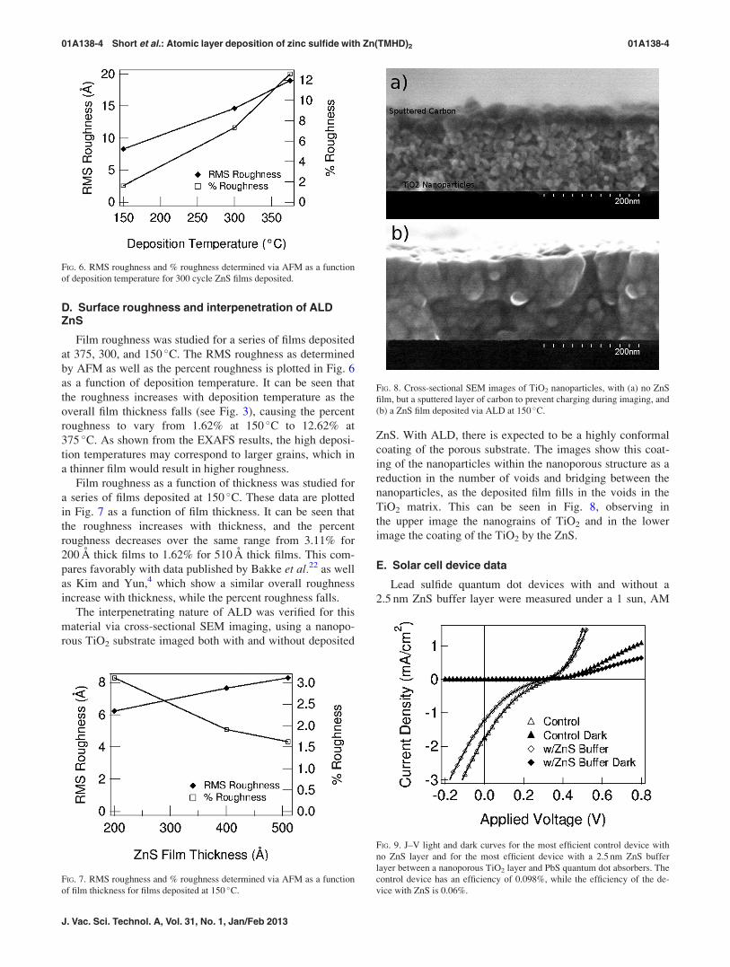
E. Solar cell device data
Lead sulfide quantum dot devices with and without a
2.5 nm ZnS buffer layer were measured under a 1 sun, AM
FIG. 6. RMS roughness and % roughness determined via AFM as a function
of deposition temperature for 300 cycle ZnS films deposited.
FIG. 7. RMS roughness and % roughness determined via AFM as a function
of film thickness for films deposited at 150 �C.
FIG. 8. Cross-sectional SEM images of TiO2 nanoparticles, with (a) no ZnS
film, but a sputtered layer of carbon to prevent charging during imaging, and
(b) a ZnS film deposited via ALD at 150 �C.
FIG. 9. J–V light and dark curves for the most efficient control device with
no ZnS layer and for the most efficient device with a 2.5 nm ZnS buffer
layer between a nanoporous TiO2 layer and PbS quantum dot absorbers. The
control device has an efficiency of 0.098%, while the efficiency of the de-
vice with ZnS is 0.06%.
01A138-4 Short et al.: Atomic layer deposition of zinc sulfide with Zn(TMHD)2 01A138-4
J. Vac. Sci. Technol. A, Vol. 31, No. 1, Jan/Feb 2013
1.5 light source (dark curves were also taken), measuring
short circuit current, open circuit voltage, fill factor, and
overall power conversion efficiency. The device stack was
quartz/ITO/sol–gel TiO2/nanoparticle TiO2/(ZnS)/nanopar-
ticle PbS/Au. Each sample consisted of six 1� 3 mm2 devi-
ces that were all functional. The J–V curves for the device of
each kind with the highest efficiency are plotted in Fig. 9.
The best device with no ZnS has a Jsc of 1.79 mA, a Voc of
0.33 V, and a fill factor of 0.165, which results in a power
conversion efficiency of 0.098%. This can be compared with
the highest efficiency device that included a 2.5 nm ZnS
buffer layer. The ZnS device has a Jsc of 1.25 mA, a Voc of
0.31 V, and a fill factor of 0.155, which results in a power
conversion efficiency of 0.06%. Despite the reduction of
overall efficiency in the device with the ZnS layer, there is
only a very small reduction in Voc indicating that the band
alignment is not affected by the ZnS layer. The data show
that the Jsc in devices with the ZnS layer drops by almost a
third, indicating poor charge transport in the devices that
contain ZnS. This may be due to an increase in series resist-
ance caused by the insulating ZnS layer.
IV. SUMMARY AND CONCLUSIONS
ZnS ALD using Zn(TMHD)2 and in situ generated H2S
has been demonstrated. The growth behavior of the films fol-
lows expected ALD behavior. Complete surface saturation
with increased dose time was not readily observed due to
precursor decomposition. Growth rates were comparable to
those in the literature for ALD of ZnS with traditional pre-
cursors. The ALD temperature dependence was investigated
from 150 to 375 �C, and the growth rate was found to
decrease over that temperature range in contrast to CVD
behavior. The band gap obtained from Tauc plots was 3.5–
3.6 eV, slightly lower than the reported literature values. The
lower band gap may be from disorder-induced band broaden-
ing, as increased disorder of the films relative to bulk ZnS
was seen in EXAFS. The EXAFS data also indicate that this
disorder increases at lower growth temperatures and at
reduced film thicknesses, and that the grain size of the grown
ZnS likely increases with temperature. The surface rough-
ness was demonstrated to be a function of deposition temper-
ature, and the depositions at the ideal parameters were
observed to penetrate within a porous matrix. Finally,
devices with a buffer layer of ZnS were studied, showing
little decrease in Voc despite a somewhat large drop in Jsc.
The device results demonstrate that the ZnS layer is acting
as a highly resistive layer between the PbS and the TiO2
with no impact on band alignment.
ACKNOWLEDGMENTS
This work was supported by the National Science Founda-
tion (Grant No. DMR-1006190). The SEM and EDX meas-
urements were conducted at the MACS center at NASA
Ames. The EXAFS experiments were carried out at the Stan-
ford Synchrotron Radiation Lightsource, operated by the
DOE, Division of Chemical Sciences. The authors thank Alli-
son Breeze of Solexant for supplying the PbS nanoparticles.
1T. Nakada, M. Mizutani, Y. Hagiwara, and A. Kunioka, Sol. Energy
Mater. Sol. Cells 67, 255 (2001).2S. M. George, Chem. Rev. 110, 111 (2010).3J. Maula, Chin. Opt. Lett. 8, 53 (2010).4Y. S. Kim and S. J. Yun, Appl. Surf. Sci. 229, 105 (2004).5C. Platzer-Bjorkman, T. Torndahl, D. Abou-Ras, J. Malmstrom, J. Kessler,
and L. Stolt, J. Appl. Phys. 100, 044506 (2006).6G. Stuyven, P. De Visschere, A. Hikavyy, and K. Neyts, J. Cryst. Growth
234, 690 (2002).7J. T. Tanskanen, J. R. Bakke, T. A. Pakkanen, and S. F. Bent, J. Vac. Sci.
Technol. A 29, 031507 (2011).8L. V. Saraf, M. H. Engelhard, C. M. Wang, A. S. Lea, D. E. McCready,
V. Shutthanandan, D. R. Baer, and S. A. Chambers, J. Mater. Res. 22,
1230 (2007).9J. D. Cox, D. D. Wagman, and V. A. Medvedev, CODATA Key Values forThermodynamics (Hemisphere, New York, 1984).
10S. Deore and A. Navrotsky, Am. Mineral. 91, 400 (2006).11G. M. Zhai, A. Bezryadina, A. J. Breeze, D. L. Zhang, G. B. Alers, and
S. A. Carter, Appl. Phys. Lett. 99, 063512 (2011).12R. G. Zhang, B. Y. Wang, and L. Wei, Vacuum 82, 1208 (2008).13P. Prathap, N. Revathi, Y. P. V. Subbaiah, and K. T. R. Reddy, J. Phys.:
Condens. Matter 20, 035205 (2008).14K. R. Murali, S. Vasantha, and K. Rajamma, Mater. Lett. 62, 1823 (2008).15Q. Liu and G. B. Mao, Surf. Rev. Lett. 16, 469 (2009).16F. Gode, C. Gumus, and M. Zor, J. Cryst. Growth 299, 136 (2007).17K. S. Rathore, D. Patidara, Y. Janu, N. S. Saxena, K. Sharma, and T. P.
Sharma, Chalcogenide Lett. 5, 105 (2008).18K. Sreejith, K. S. Mali, and C. G. S. Pillai, Mater. Lett. 62, 95 (2008).19J. P. Borah and K. C. Sarma, Acta Phys. Pol. A 114, 713 (2008).20O. L. Arenas, M. T. S. Nair, and P. K. Nair, Semicond. Sci. Technol. 12,
1323 (1997).21Z. Chen et al., J. Mater. Res. 25, 3 (2010).22J. R. Bakke, J. S. King, H. J. Jung, R. Sinclair, and S. F. Bent, Thin Solid
Films 518, 5400 (2010).23J. A. Lahtinen, A. Lu, T. Tuomi, and M. Tammenmaa, J. Appl. Phys. 58,
1851 (1985).24J. Ihanus, M. Ritala, M. Leskel€a, T. Prohaska, R. Resch, G. Friedbacher,
and M. Grasserbauer, Appl. Surf. Sci. 120, 43 (1997).25C. H. Booth, R-Space X-ray Absorption Package, 2010, see http://lise.lbl.
gov/RSXAP/.
01A138-5 Short et al.: Atomic layer deposition of zinc sulfide with Zn(TMHD)2 01A138-5
JVST A - Vacuum, Surfaces, and Films


![Microsensor Measurements ofSulfate Reduction and Sulfide ...Jorgensen1992b.pdf · constants, respectively, of the sulfide equilibrium system, [S2-] is the sulfide concentration, and](https://img.dokumen.tips/doc/110x75/5e9a6d84dc840a57bc1baa83/microsensor-measurements-ofsulfate-reduction-and-sulfide-amp-constants.jpg)