Embed Size (px)
Citation preview
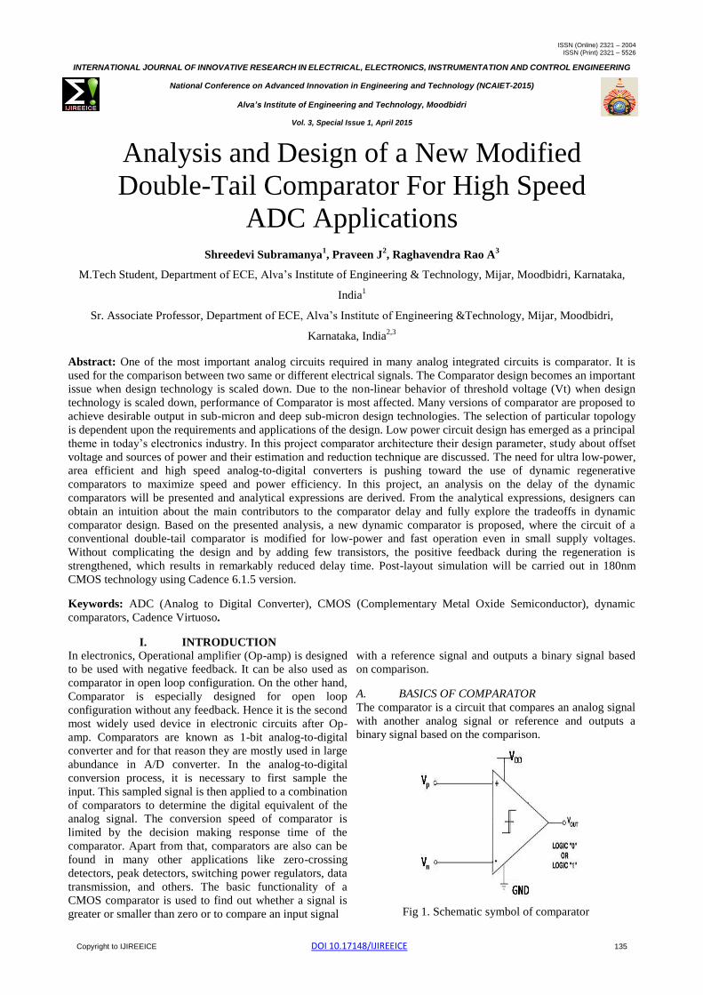
ISSN (Online) 2321 – 2004 ISSN (Print) 2321 – 5526
INTERNATIONAL JOURNAL OF INNOVATIVE RESEARCH IN ELECTRICAL, ELECTRONICS, INSTRUMENTATION AND CONTROL ENGINEERING And
National Conference on Advanced Innovation in Engineering and Technology (NCAIET-2015)
Alva’s Institute of Engineering and Technology, Moodbidri
Vol. 3, Special Issue 1, April 2015
Copyright to IJIREEICE DOI 10.17148/IJIREEICE 135
Analysis and Design of a New Modified
Double-Tail Comparator For High Speed
ADC Applications
Shreedevi Subramanya1, Praveen J
2, Raghavendra Rao A
3
M.Tech Student, Department of ECE, Alva’s Institute of Engineering & Technology, Mijar, Moodbidri, Karnataka,
India1
Sr. Associate Professor, Department of ECE, Alva’s Institute of Engineering &Technology, Mijar, Moodbidri,
Karnataka, India2,3
Abstract: One of the most important analog circuits required in many analog integrated circuits is comparator. It is
used for the comparison between two same or different electrical signals. The Comparator design becomes an important
issue when design technology is scaled down. Due to the non-linear behavior of threshold voltage (Vt) when design
technology is scaled down, performance of Comparator is most affected. Many versions of comparator are proposed to
achieve desirable output in sub-micron and deep sub-micron design technologies. The selection of particular topology
is dependent upon the requirements and applications of the design. Low power circuit design has emerged as a principal
theme in today’s electronics industry. In this project comparator architecture their design parameter, study about offset
voltage and sources of power and their estimation and reduction technique are discussed. The need for ultra low-power,
area efficient and high speed analog-to-digital converters is pushing toward the use of dynamic regenerative
comparators to maximize speed and power efficiency. In this project, an analysis on the delay of the dynamic
comparators will be presented and analytical expressions are derived. From the analytical expressions, designers can
obtain an intuition about the main contributors to the comparator delay and fully explore the tradeoffs in dynamic
comparator design. Based on the presented analysis, a new dynamic comparator is proposed, where the circuit of a
conventional double-tail comparator is modified for low-power and fast operation even in small supply voltages.
Without complicating the design and by adding few transistors, the positive feedback during the regeneration is
strengthened, which results in remarkably reduced delay time. Post-layout simulation will be carried out in 180nm
CMOS technology using Cadence 6.1.5 version.
Keywords: ADC (Analog to Digital Converter), CMOS (Complementary Metal Oxide Semiconductor), dynamic
comparators, Cadence Virtuoso.
I. INTRODUCTION
In electronics, Operational amplifier (Op-amp) is designed
to be used with negative feedback. It can be also used as
comparator in open loop configuration. On the other hand,
Comparator is especially designed for open loop
configuration without any feedback. Hence it is the second
most widely used device in electronic circuits after Op-
amp. Comparators are known as 1-bit analog-to-digital
converter and for that reason they are mostly used in large
abundance in A/D converter. In the analog-to-digital
conversion process, it is necessary to first sample the
input. This sampled signal is then applied to a combination
of comparators to determine the digital equivalent of the
analog signal. The conversion speed of comparator is
limited by the decision making response time of the
comparator. Apart from that, comparators are also can be
found in many other applications like zero-crossing
detectors, peak detectors, switching power regulators, data
transmission, and others. The basic functionality of a
CMOS comparator is used to find out whether a signal is
greater or smaller than zero or to compare an input signal
with a reference signal and outputs a binary signal based
on comparison.
A. BASICS OF COMPARATOR
The comparator is a circuit that compares an analog signal
with another analog signal or reference and outputs a
binary signal based on the comparison.
Fig 1. Schematic symbol of comparator
ISSN (Online) 2321 – 2004 ISSN (Print) 2321 – 5526
INTERNATIONAL JOURNAL OF INNOVATIVE RESEARCH IN ELECTRICAL, ELECTRONICS, INSTRUMENTATION AND CONTROL ENGINEERING And
National Conference on Advanced Innovation in Engineering and Technology (NCAIET-2015)
Alva’s Institute of Engineering and Technology, Moodbidri
Vol. 3, Special Issue 1, April 2015
Copyright to IJIREEICE DOI 10.17148/IJIREEICE 136
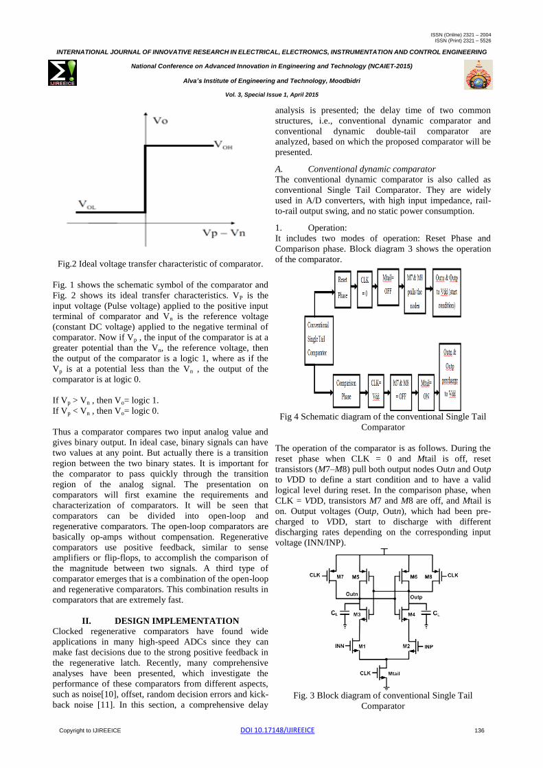
Fig.2 Ideal voltage transfer characteristic of comparator.
Fig. 1 shows the schematic symbol of the comparator and
Fig. 2 shows its ideal transfer characteristics. VP is the
input voltage (Pulse voltage) applied to the positive input
terminal of comparator and Vn is the reference voltage
(constant DC voltage) applied to the negative terminal of
comparator. Now if Vp , the input of the comparator is at a
greater potential than the Vn, the reference voltage, then
the output of the comparator is a logic 1, where as if the
Vp is at a potential less than the Vn , the output of the
comparator is at logic 0.
If Vp > Vn , then Vo= logic 1.
If Vp < Vn , then Vo= logic 0.
Thus a comparator compares two input analog value and
gives binary output. In ideal case, binary signals can have
two values at any point. But actually there is a transition
region between the two binary states. It is important for
the comparator to pass quickly through the transition
region of the analog signal. The presentation on
comparators will first examine the requirements and
characterization of comparators. It will be seen that
comparators can be divided into open-loop and
regenerative comparators. The open-loop comparators are
basically op-amps without compensation. Regenerative
comparators use positive feedback, similar to sense
amplifiers or flip-flops, to accomplish the comparison of
the magnitude between two signals. A third type of
comparator emerges that is a combination of the open-loop
and regenerative comparators. This combination results in
comparators that are extremely fast.
II. DESIGN IMPLEMENTATION
Clocked regenerative comparators have found wide
applications in many high-speed ADCs since they can
make fast decisions due to the strong positive feedback in
the regenerative latch. Recently, many comprehensive
analyses have been presented, which investigate the
performance of these comparators from different aspects,
such as noise[10], offset, random decision errors and kick-
back noise [11]. In this section, a comprehensive delay
analysis is presented; the delay time of two common
structures, i.e., conventional dynamic comparator and
conventional dynamic double-tail comparator are
analyzed, based on which the proposed comparator will be
presented.
A. Conventional dynamic comparator
The conventional dynamic comparator is also called as
conventional Single Tail Comparator. They are widely
used in A/D converters, with high input impedance, rail-
to-rail output swing, and no static power consumption.
1. Operation:
It includes two modes of operation: Reset Phase and
Comparison phase. Block diagram 3 shows the operation
of the comparator.
Fig 4 Schematic diagram of the conventional Single Tail
Comparator
The operation of the comparator is as follows. During the
reset phase when CLK = 0 and Mtail is off, reset
transistors (M7–M8) pull both output nodes Outn and Outp
to VDD to define a start condition and to have a valid
logical level during reset. In the comparison phase, when
CLK = VDD, transistors M7 and M8 are off, and Mtail is
on. Output voltages (Outp, Outn), which had been pre-
charged to VDD, start to discharge with different
discharging rates depending on the corresponding input
voltage (INN/INP).
Fig. 3 Block diagram of conventional Single Tail
Comparator
ISSN (Online) 2321 – 2004 ISSN (Print) 2321 – 5526
INTERNATIONAL JOURNAL OF INNOVATIVE RESEARCH IN ELECTRICAL, ELECTRONICS, INSTRUMENTATION AND CONTROL ENGINEERING And
National Conference on Advanced Innovation in Engineering and Technology (NCAIET-2015)
Alva’s Institute of Engineering and Technology, Moodbidri
Vol. 3, Special Issue 1, April 2015
Copyright to IJIREEICE DOI 10.17148/IJIREEICE 137
Assuming the case where VINP > VINN, Outp discharges
faster than Outn, hence when Outp (discharged by
transistor M2 drain current), falls down to VDD–|Vthp|
before Outn (discharged by transistor M1 drain current),
the corresponding pMOS transistor (M5) will turn on
initiating the latch regeneration caused by back-to-back
inverters (M3, M5 and M4, M6). Thus, Outn pulls to VDD
and Outp discharges to ground. If VINP < VINN, the
circuits works vice versa.
As shown in Fig. 4.3, the delay of this comparator is
comprised of two time delays, t0 and tlatch. The delay t0
represents the capacitive discharge of the load capacitance
CL until the first p-channel transistor (M5/M6) turns on. In
case, the voltage at node INP is bigger than INN (i.e.,
VINP > VINN), the drain current of transistor M2 (I2)
causes faster discharge of Outp node compared to the Outn
node, which is driven by M1 with smaller current.
Fig 5 Delay Characteristic response of the conventional
Single Tail Comparator
Voltage swing ΔVout = VDD/2 has to be obtained from an
initial output voltage difference ΔV0 at the falling output.
Thus delay is given by tdelay = t0+tlatch.
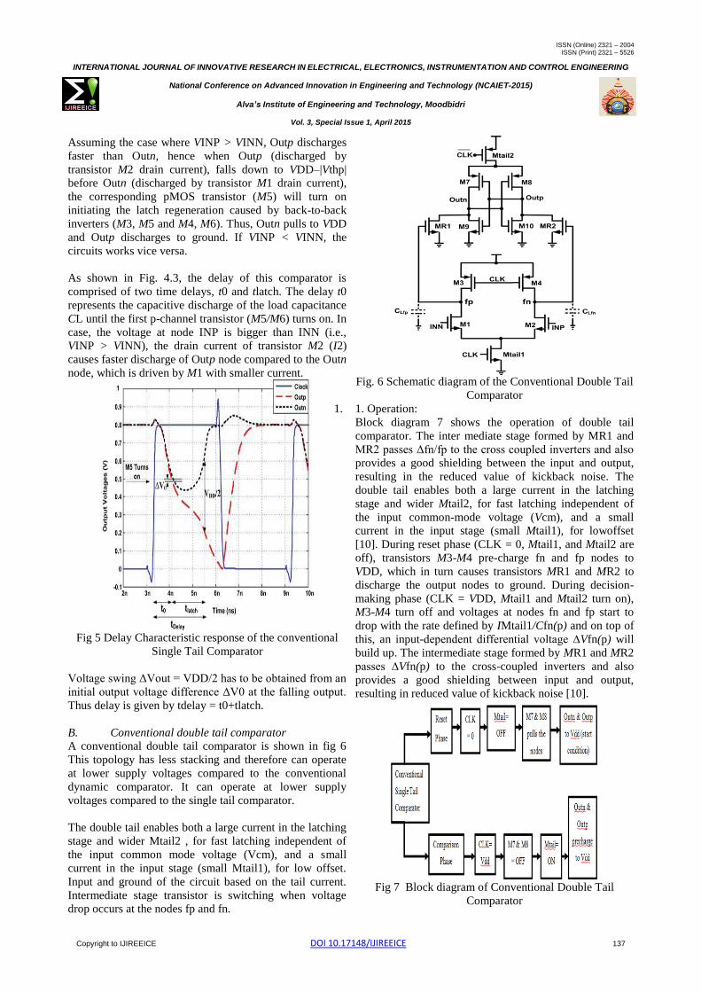
B. Conventional double tail comparator
A conventional double tail comparator is shown in fig 6
This topology has less stacking and therefore can operate
at lower supply voltages compared to the conventional
dynamic comparator. It can operate at lower supply
voltages compared to the single tail comparator.
The double tail enables both a large current in the latching
stage and wider Mtail2 , for fast latching independent of
the input common mode voltage (Vcm), and a small
current in the input stage (small Mtail1), for low offset.
Input and ground of the circuit based on the tail current.
Intermediate stage transistor is switching when voltage
drop occurs at the nodes fp and fn.
Fig. 6 Schematic diagram of the Conventional Double Tail
Comparator
1. 1. Operation:
Block diagram 7 shows the operation of double tail
comparator. The inter mediate stage formed by MR1 and
MR2 passes Δfn/fp to the cross coupled inverters and also
provides a good shielding between the input and output,
resulting in the reduced value of kickback noise. The
double tail enables both a large current in the latching
stage and wider Mtail2, for fast latching independent of
the input common-mode voltage (Vcm), and a small
current in the input stage (small Mtail1), for lowoffset
[10]. During reset phase (CLK = 0, Mtail1, and Mtail2 are
off), transistors M3-M4 pre-charge fn and fp nodes to
VDD, which in turn causes transistors MR1 and MR2 to
discharge the output nodes to ground. During decision-
making phase (CLK = VDD, Mtail1 and Mtail2 turn on),
M3-M4 turn off and voltages at nodes fn and fp start to
drop with the rate defined by IMtail1/Cfn(p) and on top of
this, an input-dependent differential voltage ∆Vfn(p) will
build up. The intermediate stage formed by MR1 and MR2
passes ∆Vfn(p) to the cross-coupled inverters and also
provides a good shielding between input and output,
resulting in reduced value of kickback noise [10].
Fig 7 Block diagram of Conventional Double Tail
Comparator

ISSN (Online) 2321 – 2004 ISSN (Print) 2321 – 5526
INTERNATIONAL JOURNAL OF INNOVATIVE RESEARCH IN ELECTRICAL, ELECTRONICS, INSTRUMENTATION AND CONTROL ENGINEERING And
National Conference on Advanced Innovation in Engineering and Technology (NCAIET-2015)
Alva’s Institute of Engineering and Technology, Moodbidri
Vol. 3, Special Issue 1, April 2015
Copyright to IJIREEICE DOI 10.17148/IJIREEICE 138
Similar to the conventional dynamic comparator, the delay
of this comparator comprises two main parts, t0 and tlatch.
The delay t0 represents the capacitive charging of the load
capacitance CLout (at the latch stage output nodes, Outn
and Outp) until the first n-channel transistor (M9/M10)
turns on, after which the latch regeneration starts; thus t0
is obtained. Total delay analysis will be carried out.
Fig 8 Delay Characteristic response of the Conventional
Double Tail Comparator.
C. Modified double tail dynamic comparator
The following Fig. 9 demonstrates the schematic diagram
of the proposed dynamic double tail comparator. Due to
the better performance of double-tail architecture in low-
voltage applications, the proposed comparator is designed
based on the double-tail structure. The main idea of the
proposed comparator is to increase ∆Vfn/fp in order to
increase the latch regeneration speed. For this purpose,
two control transistors (Mc1 and Mc2) have been added to
the first stage in parallel to M3/M4 transistors but in a
cross-coupled manner.
Fig. 9 Schematic diagram of the modified Double Tail
Dynamic Comparator
Operation of the modified Double Tail Dynamic
Comparator:
The operation of the proposed comparator is as follows.
During reset phase (CLK = 0, Mtail1 and Mtail2 are off,
avoiding static power), M3 and M4 pulls both fn and fp
nodes to VDD, hence transistor Mc1 and Mc2 are cut off.
Intermediate stage transistors, MR1 and MR2, reset both
latch outputs to ground. During decision-making phase
(CLK = VDD, Mtail1, and Mtail2 are on), transistors M3
and M4 turn off. Furthermore, at the beginning of this
phase, the control transistors are still off (since fn and fp
are about VDD). Thus, fn and fp start to drop with
different rates according to the input voltages. Suppose
VINP > VINN, thus fn drops faster than fp, (since M2
provides more current than M1). As long as fn continues
falling, the corresponding pMOS control transistor (Mc1
in this case) starts to turn on, pulling fp node back to the
VDD; so another control transistor (Mc2) remains off,
allowing fn to be discharged completely. In other words,
unlike conventional double-tail dynamic comparator, in
which _Vfn/fp is just a function of input transistor
transconductance and input voltage difference(9), in the
proposed structure as soon as the comparator detects that
for instance node fn discharges faster, a pMOS transistor
(Mc1) turns on, pulling the other node fp back to the VDD.
Therefore by the time passing, the difference between fn
and fp (∆Vfn/fp) increases in an exponential manner,
leading to the reduction of latch regeneration time.
Despite the effectiveness of the proposed idea, one of the
points which should be considered is that in this circuit,
when one of the control transistors (e.g., Mc1) turns on,a
current from VDD is drawn to the ground via input and tail
transistor (e.g., Mc1, M1, and Mtail1), resulting in static
power consumption. To overcome this issue, two nMOS
switches are used below the input transistors [Msw1 and
Msw2, as shown in Fig. 10]. At the beginning of the
decision making phase, due to the fact that both fn and fp
nodes have been pre-charged to VDD.
Fig 10 Schematic diagram of a new modified Double Tail
Comparator
ISSN (Online) 2321 – 2004 ISSN (Print) 2321 – 5526
INTERNATIONAL JOURNAL OF INNOVATIVE RESEARCH IN ELECTRICAL, ELECTRONICS, INSTRUMENTATION AND CONTROL ENGINEERING And
National Conference on Advanced Innovation in Engineering and Technology (NCAIET-2015)
Alva’s Institute of Engineering and Technology, Moodbidri
Vol. 3, Special Issue 1, April 2015
Copyright to IJIREEICE DOI 10.17148/IJIREEICE 139
Fig 11 Schematic diagram of a proposed Double Tail
Comparator
III. SIMULATION RESULTS
A. The conventional single tail comparator -
comparator 1
1. Schematic Diagram
Fig 12 Schematic diagram of the conventional Single Tail
Comparator
2. Test Setup:
Fig 13 Test setup of the conventional Single Tail
Comparator
3. Power Analysis:
Fig 14 Waveform representing Average Power of
conventional Single Tail Comparator
4. Delay Analysis:
Fig 15 Delay Characteristic response of the conventional
Single Tail Comparator
A. The conventional double tail comparator-
comparator 2
1. Schematic Diagram:
Fig 16 Schematic diagram of the Conventional Double
Tail Comparator
2. Output Waveform:
Fig.17 Output Waveform of Conventional Double Tail
Comparator
ISSN (Online) 2321 – 2004 ISSN (Print) 2321 – 5526
INTERNATIONAL JOURNAL OF INNOVATIVE RESEARCH IN ELECTRICAL, ELECTRONICS, INSTRUMENTATION AND CONTROL ENGINEERING And
National Conference on Advanced Innovation in Engineering and Technology (NCAIET-2015)
Alva’s Institute of Engineering and Technology, Moodbidri
Vol. 3, Special Issue 1, April 2015
Copyright to IJIREEICE DOI 10.17148/IJIREEICE 140
3. Power Analysis:
Fig 18 Waveform representing Average Power of
Conventional Double Tail Comparator
4. Delay Analysis :
Fig 19 Delay Characteristic response of the conventional
Double Tail Comparator
C. The modified double tail comparator-comparator
1. Schematic Diagram:
Fig 20 Schematic diagram of the modified Double Tail
Comparator
2. Test Setup:
Fig 21 Test setup of the modified Double Tail Comparator
3. Output Waveform:
Fig 22 Output Waveform of modified Double Tail
Comparator
4. Power Analysis:
Fig 23 Waveform representing Average Power of
modified Double Tail Comparator
ISSN (Online) 2321 – 2004 ISSN (Print) 2321 – 5526
INTERNATIONAL JOURNAL OF INNOVATIVE RESEARCH IN ELECTRICAL, ELECTRONICS, INSTRUMENTATION AND CONTROL ENGINEERING And
National Conference on Advanced Innovation in Engineering and Technology (NCAIET-2015)
Alva’s Institute of Engineering and Technology, Moodbidri
Vol. 3, Special Issue 1, April 2015
Copyright to IJIREEICE DOI 10.17148/IJIREEICE 141
5. Delay Analysis:
Fig 24 Delay Characteristic response of modified Double
Tail Comparator
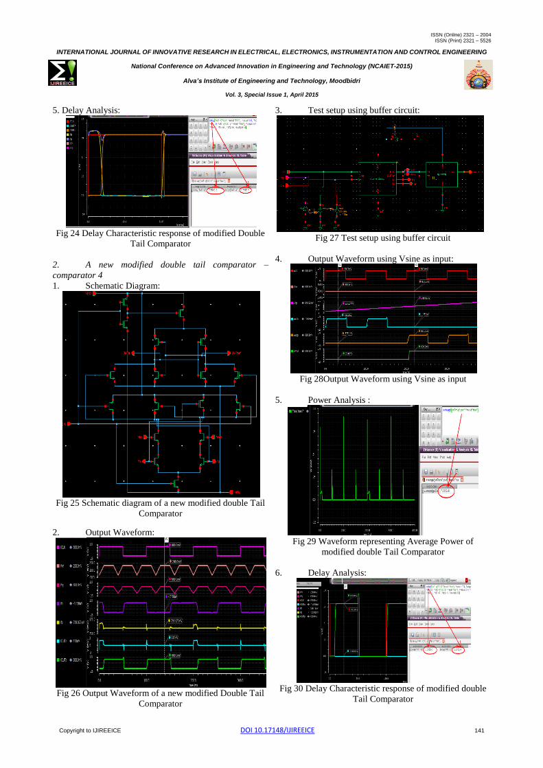
2. A new modified double tail comparator –
comparator 4
1. Schematic Diagram:
Fig 25 Schematic diagram of a new modified double Tail
Comparator
2. Output Waveform:
Fig 26 Output Waveform of a new modified Double Tail
Comparator
3. Test setup using buffer circuit:
Fig 27 Test setup using buffer circuit
4. Output Waveform using Vsine as input:
Fig 28Output Waveform using Vsine as input
5. Power Analysis :
Fig 29 Waveform representing Average Power of
modified double Tail Comparator
6. Delay Analysis:
Fig 30 Delay Characteristic response of modified double
Tail Comparator
ISSN (Online) 2321 – 2004 ISSN (Print) 2321 – 5526
INTERNATIONAL JOURNAL OF INNOVATIVE RESEARCH IN ELECTRICAL, ELECTRONICS, INSTRUMENTATION AND CONTROL ENGINEERING And
National Conference on Advanced Innovation in Engineering and Technology (NCAIET-2015)
Alva’s Institute of Engineering and Technology, Moodbidri
Vol. 3, Special Issue 1, April 2015
Copyright to IJIREEICE DOI 10.17148/IJIREEICE 142
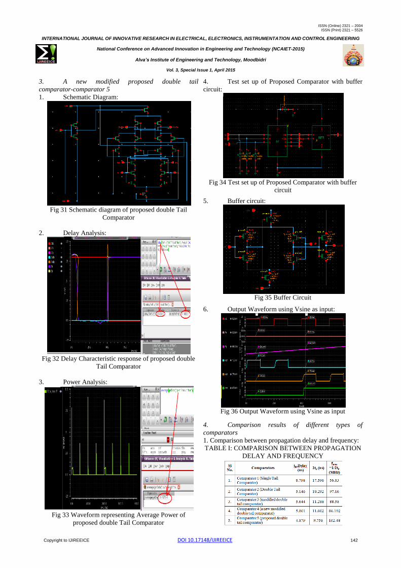
3. A new modified proposed double tail
comparator-comparator 5
1. Schematic Diagram:
Fig 31 Schematic diagram of proposed double Tail
Comparator
2. Delay Analysis:
Fig 32 Delay Characteristic response of proposed double
Tail Comparator
3. Power Analysis:
Fig 33 Waveform representing Average Power of
proposed double Tail Comparator
4. Test set up of Proposed Comparator with buffer
circuit:
Fig 34 Test set up of Proposed Comparator with buffer
circuit
5. Buffer circuit:
Fig 35 Buffer Circuit
6. Output Waveform using Vsine as input:
Fig 36 Output Waveform using Vsine as input
4. Comparison results of different types of
comparators
1. Comparison between propagation delay and frequency:
TABLE I: COMPARISON BETWEEN PROPAGATION
DELAY AND FREQUENCY

ISSN (Online) 2321 – 2004 ISSN (Print) 2321 – 5526
INTERNATIONAL JOURNAL OF INNOVATIVE RESEARCH IN ELECTRICAL, ELECTRONICS, INSTRUMENTATION AND CONTROL ENGINEERING And
National Conference on Advanced Innovation in Engineering and Technology (NCAIET-2015)
Alva’s Institute of Engineering and Technology, Moodbidri
Vol. 3, Special Issue 1, April 2015
Copyright to IJIREEICE DOI 10.17148/IJIREEICE 143
2. Comparison between power, delay and PDP :
TABLE II: COMPARISON BETWEEN POWER,
DELAY AND PDP
Fig 37 Bar Chart representation of Power, Delay and
Power-Delay Product
Fig 38 Comparison chart of Power consumption and Delay
of different comparators
3. Comparison between power consumption and
frequency:
Table III: COMPARISON BETWEEN POWER
CONSUMPTION AND FREQUENCY
IV. CONCLUSION
In this, different types of comparators are designed using
cadence GPDK 180nm. Five different types of
comparators are designed and power, delay analysis is
carried out for all. Comparator 5 (proposed double tail
comparator) gives best results and a comparison result of
different comparators has been tabulated. The Flash ADC
design will be carried out using a proposed new modified
double tail comparator.
REFERENCES [1] Sougata Ghosh, Samraat Sharma, “A Novel Low-Power, Low-
Offset and High- Speed CMOS Dynamic Latched Comparator”,
International Journal of Electronics and Computer Science Engineering, IEEE, 2010 ,Vol. 2, Number 1, pp. 411-426.
[2] Senthil Sivakumar M, Banupriya M, “ High Speed Low Power
Flash ADC Design” , International Journal of Scientific & Engineering Research, Vol. 3, Issue 5, May- 2012.
[3] “Analysis & Design of Low Power CMOS Comparator at 90nm
Technology”, Shruti Hathwalia et al Int. Journal of Engineering Research and Applications www.ijera.com ISSN: 2248-9622, Vol.
4, Issue 4( Version 1), April 2014, pp.289-292.
[4] Yavuz De˘gerli, Nicolas Fourches, Michel Rouger, and Pierre Lutz. “Low-Power Auto zeroed High- Speed Comparator” IEEE
Transaction on Nuclear Science vol. 50 no.-5 oct.2003.
[5] Nikoozadeh and B. Murmann, “An Analysis of Latch Comparator
Offset Due to Load Capacitor Mismatch,” IEEE Trans. Circuits
Syst.II, vol. 53, no. 12, pp. 1398- 1402, Dec. 2006.
[6] Daniël Schinkel, Eisse Mensink, Eric Klumperink, Ed van Tuijl, Bram Nauta, “A double-tail latch-type voltage sense amplifier with
18ps Setup+Hold time”,
[7] Heungjun Jeon and Yong-Bin Kim, “A Novel Low-Power, Low-Offset and High-Speed CMOS Dynamic Latched Comparator”,
IEEE press, 2010.
[8] Shaik Mastan Vali1, Pyla Rajesh, “A 3GHz Low-offset Fully Dynamic Latched Comparator for High-Speed and Low-Power
ADCs” International Journal of Emerging Technology and
Advanced Engineering, Volume 3, Issue 6, June 2013. [9] “Analysis and design of a low-voltage low-power double-tail
comparator”, proposed by Samaneh and Reza Lotfi, IEEE transactions on Very Large Scale Integration (VLSI) systems, vol.
22, no. 2, February 2014.
[10] Umamaheswari.V. S .,Rajaramya.G2, “Low Power High Performance Double-tail Comparator” , ISSN : 2277-1581,May
2014.
020406080
100120
Power(µW)
0
2
4
6
8
10
12 Power(µW)
Delay(ns)


![A High-Speed 64-Bit Binary Comparator€¦ · A high-speed 64-bit binary comparator 39 | Page III. EXISTING 64-BIT BINARY COMPARATOR DESIGN 64-bit comparator in reference [8], [9],](https://img.dokumen.tips/doc/110x75/5eac1a458d19873e777698b4/a-high-speed-64-bit-binary-comparator-a-high-speed-64-bit-binary-comparator-39-.jpg)