Embed Size (px)
Citation preview

AN2497Designing Digital RF Receiver Using MCP37DXX High-Speed ADC
INTRODUCTION
In recent years, digital RF receiver technology has madesignificant progress, mainly due to the availability ofhigh-speed ADCs. The direct conversion, IF samplingand software defined radio architectures are becomingcommon practice in the modern RF receiver design.
Due to ongoing advances in chip manufacturing andADC design technologies, many of the Digital SignalProcessing (DSP) functions, which used to be in sepa-rate devices or done by software, are now included inthe ADC itself.
For example, the MCP37XXX high-speed ADC includesvarious programmable Digital Signal Processing build-ing blocks for specific applications, such as (a) DigitalDown-Conversion for in-phase and quadrature signaldetection, (b) digital decimation filtering for higherSignal-to-Noise Ratio (SNR) and (c) Continuous-Wave(CW) beamforming for the phase correction of acquiredsignals from multiple inputs, such as signals fromphased array antennas or ultrasound transducers.
These built-in digital building blocks can greatly reducethe overall system hardware requirements, while alsoimproving the system performance. The reducedsystem component requirements and lower power con-sumption enable lower overall system cost, and makeportable system design much easier and simpler[4].
FIGURE 1: Block Diagram of Digitally Enhanced ADC with Built-In Digital Signal Post-Processing Features[1-2].
Author: Youbok Lee, Ph.D.Microchip Technology Inc.
Output Control:- CMOS, DDR LVDS- Serialized LVDS
Digital Signal Post-Processing:- Fractional Delay Recovery (FDR)- Decimation- Digital Down-Conversion (DDC)- CW Beamforming- Phase/Offset/Gain Adj.
CLK+
CLK-
AIN0+AIN0-
AIN7+AIN7-
VCM
SENSE
VBG
REF1+ REF1- REF0+ REF0- SDIO SCLK CS
ReferenceGenerator
VREF+ VREF-
PipelinedADC Core
Data
DCLK+
DCLK-
AVDD12 AVDD18 GND DVDD12 DVDD18
Duty CycleSelectionClock
Selection
Inp
ut M
ulti
plex
er
Output Clock Control
Internal Registers
DLL
PLL
2018 Microchip Technology Inc. DS00002497A-page 1

AN2497
BUILT-IN DIGITAL SIGNAL PROCESSING BUILDING BLOCKS[1-3]
Figure 1 shows a simplified block diagram of amulti-channel high-speed ADC with built-in DigitalSignal Post-Processing (DSPP) features. The analoginput signal is digitized by the ADC core andpost-processed internally, depending on the user’sselection, before the digital output is available at theoutput pins.
The optional DSPP features are (a) Fractional DelayRecovery, (b) decimation, (c) Digital Down-Conversion,(d) CW beamforming and (e) phase/offset/gain adjust-ment per channel. These digital options are selectableusing user Configuration register bit settings, whichare dynamically programmable on the fly. Table 1summarizes these Digital Signal Processing options.
TABLE 1: BUILT-IN DIGITAL SIGNAL POST-PROCESSING FEATURES
Features Descriptions Applications Availability
Fractional Delay Recovery (FDR)
Digitally compensates the time delay of the sampling events between input channels. Without using FDR, the input sampling time difference between adjacent channels is 1 ADC core clock cycle. When FDR is enabled, the time difference is synthetically reduced to less than 1 ns.
This feature is only needed in Multichannel mode.
Available in Dual and Octal-Channel mode only. In other modes, the FDR can be done by software in the host device if needed.
Decimation Finite Impulse Response (FIR) decimation filter for higher SNR. When applied, the output data throughput is reduced by the decimation factor, N.
This is a preferred option for high-resolution imaging applications or when higher SNR is needed.
• Single and Dual Channel modes
• CW Octal-Channel mode
Digital Down-Conversion(DDC)
In-Phase and Quadrature Component Detection: • Shifts the input frequency spectrum to lower
frequency band.• Outputs the resulting signal as either I/Q data
or as a real signal centered at ¼ of the output data rate.
• Software defined radio• Wireless communications,
including: radar, sonar, ultrasound sensors, etc.
• Single and Dual Channel modes
• CW Octal-Channel mode
CW Beamforming In octal-channel configuration, beamforming is used to correct the time delay of the incoming signals (at input pin) with respect to the reference. The beam-forming is achieved by controlling the phase and gain of each input channel individually.
• Octal-channel transducers for ultrasound/sonar
• Phased array antenna
Octal-Channel mode only.
Phase/Offset/ Gain Adjustment per Each Channel.
Digital correction of phase, offset and gain of individual channel.
— Available for all Channel modes.
DS00002497A-page 2 2018 Microchip Technology Inc.

AN2497
USING FRACTIONAL DELAY RECOVERY (FDR) FOR MULTICHANNEL CONFIGURATION[1]
When the device is used in Multichannel mode, itsamples the channel inputs sequentially using a MUX,while the single ADC core is operating at a constant fullspeed. This sequential sampling of multiple channelsintroduces a time delay between the sampling of differ-ent input channels relative to a multicore ADC, whichsamples all inputs at the same instant. The FractionalDelay Recovery (FDR) option digitally compensatesthe time delay of the sampling events.
When the FDR is enabled, a high-order, band limitedinterpolation filter deskews the sampling instant withina limited input bandwidth and synthetically removes thetime delay of the input sampling. The FDR is availablein Dual Channel and Octal-Channel modes.
USING DIGITAL DECIMATION FILTER[1-3]
The Finite Impulse Response (FIR) decimation filter canbe applied when a higher SNR is needed or to provideout-of-band rejection for the desired signal. The outputbandwidth of the FIR filter is reduced by the decimationfactor, N. The final output bandwidth of the FIR filter isdetermined by dividing the ADC sampling rate by N.
In conventional applications, the digital decimation istypically processed at the host computing device. Thisprocess takes extra resource time from the computingdevice and can delay the decision-making process.Instead, this decimation filter can be applied within theADC before the digital output is available to the hostdevice, reducing the resource overhead of the computingdevice.
Figure 2 shows the performance of a 16-bit 200 MspsADC before any decimation is applied. The ADCachieves an SNR of 74.7 dBFS. Table 1 shows theoverall SNR performance versus decimation settings.The SNR is improved with higher decimation rates.About 2.5 dB improvement is achieved per step (2x perstep), up to a decimation rate of 128x. The SNRimprovement becomes almost flat after the decimationrate reaches about 128x. An SNR of 92.3 dBFS can beachieved with the 512x decimation setting using the200 Msps 16-bit ADC. This is a significant improvementcompared to the performance of typical high-speed ADCswithout this feature. See Reference [1-3] for more detailson using the digital decimation filter.
FIGURE 2: FFT of 200 Msps 16-Bit ADC Output:[1] Input (FIN) = 30.2177 MHz @ -1.2 dBFS, SNR = 74.7 dBFS, SFDR = 90.1 dBc.
TABLE 2: DECIMATION RATE vs. SNR PERFORMANCE
Decimation RateSNR (dBFS)
16-Bit Output Mode
8x 82.3
16x 84.8
32x 87.1
64x 89.2
128x 91.0
256x 92.0
512x 92.3
2018 Microchip Technology Inc. DS00002497A-page 3

AN2497
USING DIGITAL DOWN-CONVERSION (DDC) FEATURE FOR WIRELESS APPLICATIONS[1-4]
Figure 3 shows a simplified block diagram of the built-inDDC configuration. The DDC includes a 32-bit complexNumerically Controlled Oscillator (NCO), a selectable(high/low) half-band filter, optional decimation filters andtwo Output modes (I/Q or fS/8). Frequency translation isaccomplished by the NCO. The NCO frequency isprogrammable, anywhere from 0 Hz to the input SamplingFrequency (fs). Phase and amplitude dither can beenabled to improve spurious performance of the NCO.
Each of the processing sub-blocks are individuallycontrolled using register settings. This DDC feature canbe used to simplify various RF receiving system
designs and to reduce system cost. Figure 6 shows anexample of Software Defined Radio (SDR) using theMCP37DXX. As shown in the figure, the entire digital IFblock in the SDR can be replaced with a singleMCP37DXX.
The FFT output from the ADC core is shown in Figure 2for a 30.2177 MHz input signal. When the NCO is setat 31 MHz, the I/Q signals appear at 0.7823 MHz.Figure 4 shows the I/Q output signals: (a) when thedecimation filter is not applied and (b) when thedecimation filter (16x) is applied. Figure 5 shows theoutput signal when upconverted by fS/8/DER, whereDER is the decimation rate applied (16x). SeeReference [1-4] for more details on the DigitalDown-Conversion feature.
.
FIGURE 3: Built-In Digital Down-Conversion (DDC) Block Diagram for Single Channel Device.
FIGURE 4: FFT of In-Phase and Quadrature Signal after Digital Down-Conversion.
FIGURE 5: FFT of Upconverter Output.
NCO (32-bit)
I
Q
Down-Converting and Decimation Decimation and Output Frequency Translation
FIR ADecimation Filter
Real orNCO ( )
fS/8DER
cos sin
FIR BDecimation Filter
I or IDEC
Q or QDEC
RealDEC
Half-Band Filter A
LP/HP
(a) FFT of I/Q signal before decimation filter is applied.
(b) FFT of I/Q signal after decimation filter is applied.
DS00002497A-page 4 2018 Microchip Technology Inc.

AN2497
USING DIGITAL DOWN-CONVERSION FOR SOFTWARE DEFINED RADIO (SDR)
Figure 6 shows an example of a software defined radioreceiver employing a super-heterodyne, dual stage con-version architecture. This architecture is popularly usedin various modern digital RF communication systems,including LTE, IEEE 802.11. The received RadioFrequency (RF) signal is down-converted to anIntermediate Frequency (IF) in the first stage and thenconverted to baseband signals in the second stage. Thesecond stage includes an ADC, which digitizes the IFsignal, and a Digital Down-Conversion circuit, whichconverts the digitized IF signal to the in-phase andquadrature baseband signals. The DigitalDown-Conversion block includes a NumericallyControlled Oscillator (NCO), digital mixers, I/Qdemodulation and FIR decimation filters.
In a conventional digital radio architecture, the DigitalDown-Conversion is typically achieved by extensive firm-ware operations using a high-end Field ProgrammableGate Array (FPGA) device. The firmware developmentand management are very time-consuming tasks for thesystem designers. Additionally, the FPGA tends to bethe highest cost component in many systems.
Instead of implementing the digital IF processingblock with discrete components, or using extensiveFPGA-based logic, system designers can now utilizethe built-in Digital Down-Conversion (DDC) featurein the MCP37DXX ADC. As shown in Figure 6, theMCP37DXX minimizes the RF components neededfor the RF receiver design and simplifies the systemarchitecture.
FIGURE 6: Example of Using the MCP37DXX for Software Defined Radio.
MCP37DXX
Amp/FilterDSP
I
Q
2018 Microchip Technology Inc. DS00002497A-page 5
AN2497
USING DIGITAL BEAMFORMING[1-3]
Digital beamforming is widely used in the sonar, radarand ultrasound imaging systems, where multipleantenna/transducers are used. When a large numberof antennas/transducers is used, the signals from eachreceiving element arrive at the detection device with adifferent time delay. Also, in multichannel scanningoperations using the MUX, there is a time delaybetween acquiring input signals. These time delays canbe corrected before all input signals are combined forthe final signal processing.
The time delay correction involves the phase alignmentof the detected signals with respect to a reference.
The MCP37D31/21-200 device has built-in Continuous-Wave (CW) digital beamforming and Doppler signalprocessing features, which are available in theoctal-channel operation only. These features cansignificantly simplify the conventional beamformingcircuits.
Figure 7 shows a simplified block diagram for continu-ous beamforming with the DDC I/Q decimation stage.The device achieves beamforming by scanning allinputs while correcting the phase of each channel withrespect to a reference. This can be done using:[1]
• Fractional Delay Recovery (FDR)
• Phase offset settings of each individual channel
• Gain setting per channel
While the input channel is multiplexed sequentially, thephase offset can be added to the NCO output (eachchannel individually), which corrects the time delay ofthe incoming signals with respect to the reference[1].
The phase compensated input signal is then down-converted by a wide dynamic range I/Q demodulatorstage. The digital beamforming of the inputs is thenobtained by summing I and Q data from individual chan-nels. This summed I and Q data are fed to the half-bandfilter. Equation 1 shows the I and Q data of an individualchannel with phase, gain and offset correction, and theresulting digital beamforming signal.
The processing blocks, after the digital beamforming, arethe same as for the DDC single channel operation[1].
EQUATION 1: BEAMFORMING SIGNALS
.
FIGURE 7: Digital Beamforming Block Diagram in Octal-Channel Configuration[1].
ICH n ADC n G COS 2fNCOt n + =
QCH n ADC n G SIN 2fNCOt n + =
I ICH n n 0=
N
= Q QCH n n 0=
N
=
Where:
ADC(n) = ADC output of Channel n
= Digital offset adjustment of Channel n
G = Digital gain adjustment of Channel n
(n) = NCO phase offset of Channel n
and
CH. 0
CH. 7
EN_DDC1
MCP37DXX
Half-Band
LP/HP
NCO (32-bit)
FIR A Decimation Filter
NCO Phase Offset Control
NCO Amplitude Dither
Sine/CosineSignal Generator
NCO Phase Dither
QCH(n)cos sin
FIR BDecimation Filter
I or IDEC
Q or QDEC
Digital Down-Converting and Digital Beamforming
Decimation
ICH(n)
EN_DDC2
NCO ( )fS/8DER
Real orRealDEC
Frequency Upshifting if Needed
ADC Core8-CH
Filter A
DS00002497A-page 6 2018 Microchip Technology Inc.

AN2497
USING DIGITAL BEAMFORMING FOR ULTRASOUND IMAGING SYSTEMS
Figure 8 shows a simplified block diagram for the ultra-sound imaging system, which utilizes analog and digitalbeamforming with DDC I/Q decimation.
The digital beamforming that is performed inside theFPGA unit can be achieved using the built-in featureset in the MCP37DXX.
Doppler shift measurement requires summing the inputsignals from multiple transducer channels and mixingthem with a phase controlled local oscillator frequency.
The resulting low-frequency output is then centerednear DC and can measure a Doppler shift produced bymoving objects, such as blood flow, changes in bloodpressure in arteries, etc. The I/Q outputs that representthe Doppler shift can be processed using the 1 Msps16-bit SAR ADCs, such as MCP33131.
The MX57XXX and DSC400 clock devices fromMicrochip can be used to provide the timing source ofeach building block.
FIGURE 8: Example of Ultrasound Imaging System Building Block.
BeamformerCentral Control ProcessorIsolationDACHV
Amp
T/R Switches LNA VGAHigh-Speed
Clocks
Amp
Amp
ADC
ADC
CWDoppler
Processing
ImageMotion
Processing(B-Mode)
ColorDoppler
(F-Mode)Processing
VideoCompression
Video DAC/Video Encoder
Amp/Filter
Amp/Filter
I/Q Processing
AudioDAC
FPGA/High-End MCUDigital RX Beamformer
LNA-VGA-ADC Array (up to 256 channels)
MCP33131(1 Msps 16-bit ADC)
MX57XXXXDSC400
MCP37DXX
HV MUX
DEMUX
TX/RXSwitch
ADC
TransducerCW AnalogBeamformer
I
Q
2018 Microchip Technology Inc. DS00002497A-page 7

AN2497
USING MCP37DXX FOR SONAR SYSTEMS
Figure 9 shows an example of a receiver block diagramfor Sonar. The octal-channel MCP37DXX is an idealdevice for the Sonar receiver design. The device’sDDC and digital beamforming feature can be utilized.
In Octal-Channel mode, the amplitude and time delayof the incoming signals of each channel are digitallycorrected, with respect to the reference. The digitalbeamforming of the inputs is then obtained by summingI and Q signals from individual channels.
The Doppler signal information for the moving targetcan be easily extracted from the I and Q data.
FIGURE 9: Sonar Receiver Block Diagram Utilizing the Beamforming Feature of the 8-Channel MCP37DX1.
Note: The digital beamforming is available inOctal-Channel mode only. Other thanOctal-Channel mode, the offset and gaincontrol for each individual channel is stillavailable, except the phase control.
MCP37DX1Transducer
LNA
BPF
n = 1
n = 8
NCO (32-bit)
NCO Phase Offset Control
NCO Amplitude Dither
NCO Phase Dither
QCH(n)cos sin
FIR BDecimation Filter
I or IDEC
Q or QDECADC Core
Digital Beamforming
DDC
ICH(n)
8-CH
Sine/CosineSignal Generator
Half-Band Filter ALP/HP
FIR ADecimation Filter
DS00002497A-page 8 2018 Microchip Technology Inc.

AN2497
EXTERNAL TIME-INTERLEAVING FOR HIGHER SPEED DATA CONVERSIONS[1-3]
Figure 10 shows an example of achieving externaltiming-interleaving for higher data conversion. As anexample, 800 Msps time-interleaved conversion can
be achieved by using four 200 Msps devices. Thisconfiguration can be used for digital oscilloscopedesign. For 1 Gsps conversion, the user can operatethe four ADCs with a 250 MHz clock with 90 degreephase difference.
.
FIGURE 10: Time-Interleaved Configuration for Higher Speed Data Conversion.
Note: Each device samples input at the its own clock phase.
CLK (0°)
CLK (90°)
CLK (180°)
CLK (270°)
Device 1 (Slave 1)
Device 2 (Slave 2)
Device 3 (Slave 3)
Master
(SLAVE Pin = Tie to GND)
(Slave Devices: SLAVE Pin = Tie to DVDD)
(SYNC)
(SYNC)
(SYNC)
(b) Clocks for each device.
(a) External clock phase control in Auto-Sync mode.
2018 Microchip Technology Inc. DS00002497A-page 9
AN2497
POWER CONSUMPTION
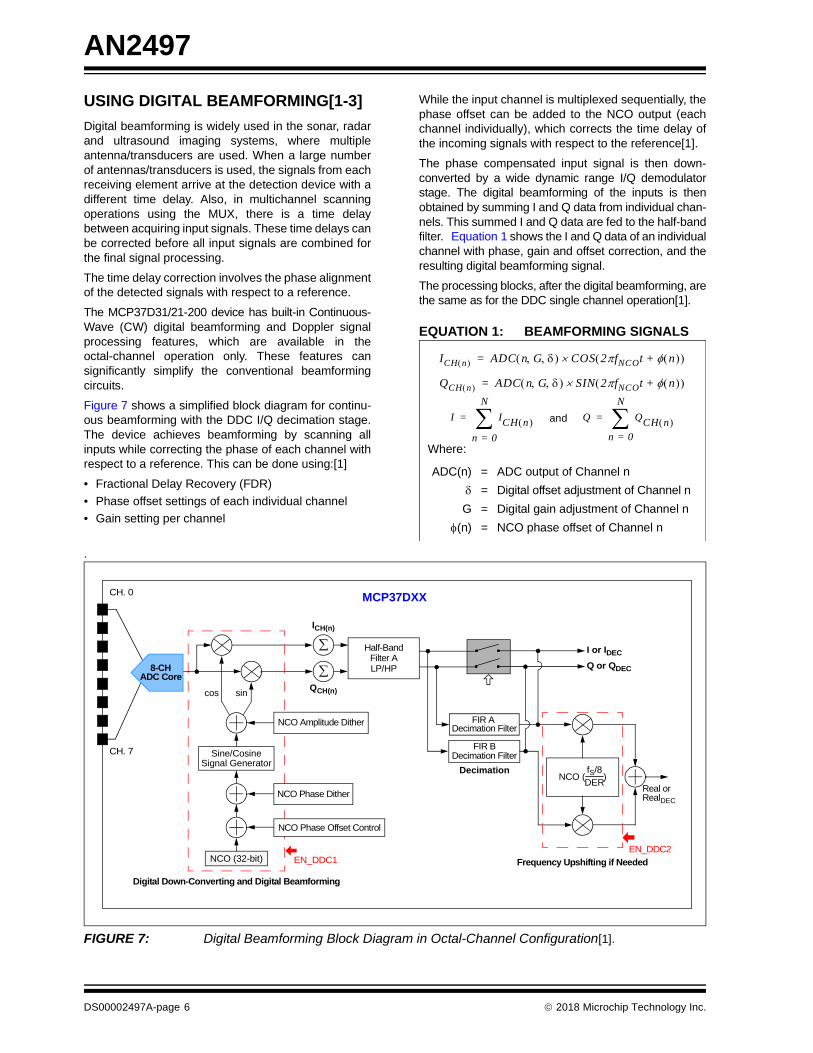
In RF system design, meeting the system power budgetis an important criteria, which is especially needed forportable applications, such as oscilloscopes and hand-held data acquisition devices. With advanced ADCdesign and manufacturing technology, the digitallyenhanced high-speed ADC of today can be designedwith very low-power consumption. The power consump-tion of this ADC core is about 490 mW for a 16-bit,200 Msps device with LVDS output and 338 mW for a12-bit, 200 Msps device with LVDS output[1-2].Figure 11 shows the power consumption of a singlechannel 14-bit, 200 Msps device over input samplingrates[2].
FIGURE 11: Power Consumption vs. Sampling Frequency of the Digitally Enhanced ADC: Single Channel, 14-Bit Device[2].
CONCLUSIONS
The built-in digital blocks in the MCP37DXX ADC cansimplify modern digital receiver designs. Dynamicallyreconfigurable features improve the overall systemperformance and allow for improved system designflexibility. By utilizing the built-in digital features, theoverall receiving system components can be reducedsignificantly, which allows miniaturization of the RFreceiver. The low-power consumption of the digitallyenhanced ADC offers an excellent solution forpower-sensitive portable device designs. RF designersshould take advantage of all these available options fortheir RF system designs.
REFERENCES
[1] “MCP37231/21-200/MCP37D31/21-200 Family Data Sheet” (DS20005322), Microchip Technology Inc., 2014-2016.
[2] “MCP37220-200/MCP37D20-200 Family Data Sheet” (DS20005396), Microchip Technology Inc., 2015-2016.
[3] “MCP37210-200/MCP37D10-200 Family Data Sheet” (DS20005395), Microchip Technology Inc., 2015-2016.
[4] Thomas Youbok Lee, Andrea Panigada, Dan Meacham, Trent Butcher, Toshikazu Ishida, “Digitally Enhanced High Speed ADC for Low-Power Wireless Applications”, IEEE MTT-S International Conference on Microwaves for Intelligent Mobility (ICMIM), Nagoya, Japan, March 20, 2017.
DS00002497A-page 10 2018 Microchip Technology Inc.
AN2497
APPENDIX A: DEVELOPMENT SUPPORT
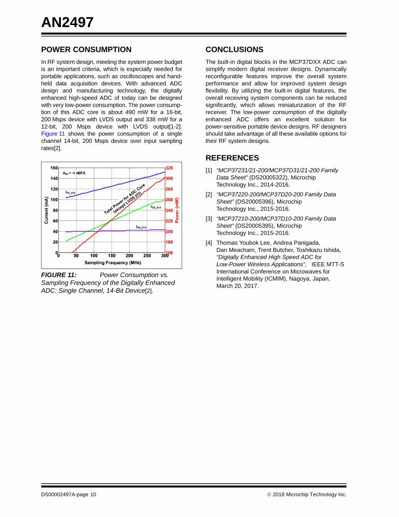
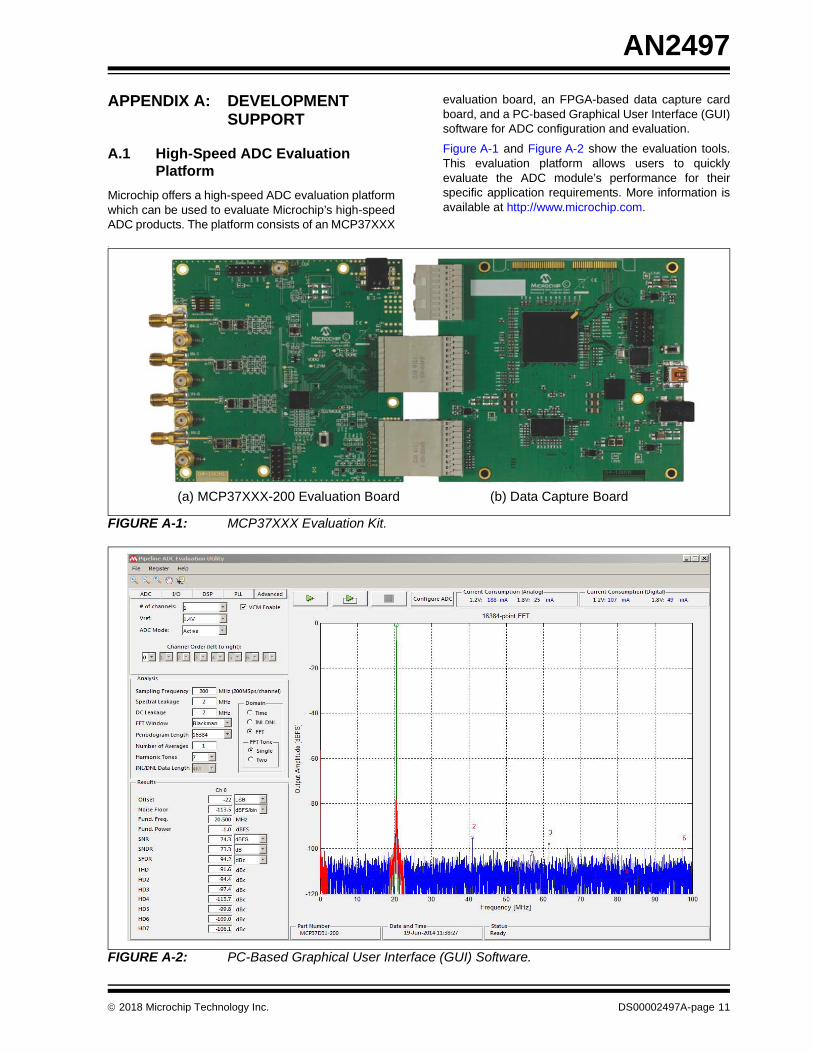
A.1 High-Speed ADC Evaluation Platform
Microchip offers a high-speed ADC evaluation platformwhich can be used to evaluate Microchip’s high-speedADC products. The platform consists of an MCP37XXX
evaluation board, an FPGA-based data capture cardboard, and a PC-based Graphical User Interface (GUI)software for ADC configuration and evaluation.
Figure A-1 and Figure A-2 show the evaluation tools.This evaluation platform allows users to quicklyevaluate the ADC module’s performance for theirspecific application requirements. More information isavailable at http://www.microchip.com.
.
FIGURE A-1: MCP37XXX Evaluation Kit.
FIGURE A-2: PC-Based Graphical User Interface (GUI) Software.
(b) Data Capture Board(a) MCP37XXX-200 Evaluation Board
2018 Microchip Technology Inc. DS00002497A-page 11

AN2497
NOTES:
DS00002497A-page 12 2018 Microchip Technology Inc.
Note the following details of the code protection feature on Microchip devices:
• Microchip products meet the specification contained in their particular Microchip Data Sheet.
• Microchip believes that its family of products is one of the most secure families of its kind on the market today, when used in the intended manner and under normal conditions.
• There are dishonest and possibly illegal methods used to breach the code protection feature. All of these methods, to our knowledge, require using the Microchip products in a manner outside the operating specifications contained in Microchip’s Data Sheets. Most likely, the person doing so is engaged in theft of intellectual property.
• Microchip is willing to work with the customer who is concerned about the integrity of their code.
• Neither Microchip nor any other semiconductor manufacturer can guarantee the security of their code. Code protection does not mean that we are guaranteeing the product as “unbreakable.”
Code protection is constantly evolving. We at Microchip are committed to continuously improving the code protection features of ourproducts. Attempts to break Microchip’s code protection feature may be a violation of the Digital Millennium Copyright Act. If such actsallow unauthorized access to your software or other copyrighted work, you may have a right to sue for relief under that Act.
Information contained in this publication regarding deviceapplications and the like is provided only for your convenienceand may be superseded by updates. It is your responsibility toensure that your application meets with your specifications.MICROCHIP MAKES NO REPRESENTATIONS ORWARRANTIES OF ANY KIND WHETHER EXPRESS ORIMPLIED, WRITTEN OR ORAL, STATUTORY OROTHERWISE, RELATED TO THE INFORMATION,INCLUDING BUT NOT LIMITED TO ITS CONDITION,QUALITY, PERFORMANCE, MERCHANTABILITY ORFITNESS FOR PURPOSE. Microchip disclaims all liabilityarising from this information and its use. Use of Microchipdevices in life support and/or safety applications is entirely atthe buyer’s risk, and the buyer agrees to defend, indemnify andhold harmless Microchip from any and all damages, claims,suits, or expenses resulting from such use. No licenses areconveyed, implicitly or otherwise, under any Microchipintellectual property rights unless otherwise stated.
2018 Microchip Technology Inc.
Microchip received ISO/TS-16949:2009 certification for its worldwide headquarters, design and wafer fabrication facilities in Chandler and Tempe, Arizona; Gresham, Oregon and design centers in California and India. The Company’s quality system processes and procedures are for its PIC® MCUs and dsPIC® DSCs, KEELOQ® code hopping devices, Serial EEPROMs, microperipherals, nonvolatile memory and analog products. In addition, Microchip’s quality system for the design and manufacture of development systems is ISO 9001:2000 certified.
QUALITY MANAGEMENT SYSTEM CERTIFIED BY DNV
== ISO/TS 16949 ==
Trademarks
The Microchip name and logo, the Microchip logo, AnyRate, AVR, AVR logo, AVR Freaks, BeaconThings, BitCloud, CryptoMemory, CryptoRF, dsPIC, FlashFlex, flexPWR, Heldo, JukeBlox, KEELOQ, KEELOQ logo, Kleer, LANCheck, LINK MD, maXStylus, maXTouch, MediaLB, megaAVR, MOST, MOST logo, MPLAB, OptoLyzer, PIC, picoPower, PICSTART, PIC32 logo, Prochip Designer, QTouch, RightTouch, SAM-BA, SpyNIC, SST, SST Logo, SuperFlash, tinyAVR, UNI/O, and XMEGA are registered trademarks of Microchip Technology Incorporated in the U.S.A. and other countries.
ClockWorks, The Embedded Control Solutions Company, EtherSynch, Hyper Speed Control, HyperLight Load, IntelliMOS, mTouch, Precision Edge, and Quiet-Wire are registered trademarks of Microchip Technology Incorporated in the U.S.A.
Adjacent Key Suppression, AKS, Analog-for-the-Digital Age, Any Capacitor, AnyIn, AnyOut, BodyCom, chipKIT, chipKIT logo, CodeGuard, CryptoAuthentication, CryptoCompanion, CryptoController, dsPICDEM, dsPICDEM.net, Dynamic Average Matching, DAM, ECAN, EtherGREEN, In-Circuit Serial Programming, ICSP, Inter-Chip Connectivity, JitterBlocker, KleerNet, KleerNet logo, Mindi, MiWi, motorBench, MPASM, MPF, MPLAB Certified logo, MPLIB, MPLINK, MultiTRAK, NetDetach, Omniscient Code Generation, PICDEM, PICDEM.net, PICkit, PICtail, PureSilicon, QMatrix, RightTouch logo, REAL ICE, Ripple Blocker, SAM-ICE, Serial Quad I/O, SMART-I.S., SQI, SuperSwitcher, SuperSwitcher II, Total Endurance, TSHARC, USBCheck, VariSense, ViewSpan, WiperLock, Wireless DNA, and ZENA are trademarks of Microchip Technology Incorporated in the U.S.A. and other countries.
SQTP is a service mark of Microchip Technology Incorporated in the U.S.A.
Silicon Storage Technology is a registered trademark of Microchip Technology Inc. in other countries.
GestIC is a registered trademark of Microchip Technology Germany II GmbH & Co. KG, a subsidiary of Microchip Technology Inc., in other countries.
All other trademarks mentioned herein are property of their respective companies.
© 2018, Microchip Technology Incorporated, All Rights Reserved.
ISBN: 978-1-5224-3178-7
DS00002497A-page 13
DS00002497A-page 14 2018 Microchip Technology Inc.
AMERICASCorporate Office2355 West Chandler Blvd.Chandler, AZ 85224-6199Tel: 480-792-7200 Fax: 480-792-7277Technical Support: http://www.microchip.com/supportWeb Address: www.microchip.com
AtlantaDuluth, GA Tel: 678-957-9614 Fax: 678-957-1455
Austin, TXTel: 512-257-3370
BostonWestborough, MA Tel: 774-760-0087 Fax: 774-760-0088
ChicagoItasca, IL Tel: 630-285-0071 Fax: 630-285-0075
DallasAddison, TX Tel: 972-818-7423 Fax: 972-818-2924
DetroitNovi, MI Tel: 248-848-4000
Houston, TX Tel: 281-894-5983
IndianapolisNoblesville, IN Tel: 317-773-8323Fax: 317-773-5453Tel: 317-536-2380
Los AngelesMission Viejo, CA Tel: 949-462-9523Fax: 949-462-9608Tel: 951-273-7800
Raleigh, NC Tel: 919-844-7510
New York, NY Tel: 631-435-6000
San Jose, CA Tel: 408-735-9110Tel: 408-436-4270
Canada - TorontoTel: 905-695-1980 Fax: 905-695-2078
ASIA/PACIFICAustralia - SydneyTel: 61-2-9868-6733
China - BeijingTel: 86-10-8569-7000
China - ChengduTel: 86-28-8665-5511
China - ChongqingTel: 86-23-8980-9588
China - DongguanTel: 86-769-8702-9880
China - GuangzhouTel: 86-20-8755-8029
China - HangzhouTel: 86-571-8792-8115
China - Hong Kong SARTel: 852-2943-5100
China - NanjingTel: 86-25-8473-2460
China - QingdaoTel: 86-532-8502-7355
China - ShanghaiTel: 86-21-3326-8000
China - ShenyangTel: 86-24-2334-2829
China - ShenzhenTel: 86-755-8864-2200
China - SuzhouTel: 86-186-6233-1526
China - WuhanTel: 86-27-5980-5300
China - XianTel: 86-29-8833-7252
China - XiamenTel: 86-592-2388138
China - ZhuhaiTel: 86-756-3210040
ASIA/PACIFICIndia - BangaloreTel: 91-80-3090-4444
India - New DelhiTel: 91-11-4160-8631
India - PuneTel: 91-20-4121-0141
Japan - OsakaTel: 81-6-6152-7160
Japan - TokyoTel: 81-3-6880- 3770
Korea - DaeguTel: 82-53-744-4301
Korea - SeoulTel: 82-2-554-7200
Malaysia - Kuala LumpurTel: 60-3-7651-7906
Malaysia - PenangTel: 60-4-227-8870
Philippines - ManilaTel: 63-2-634-9065
SingaporeTel: 65-6334-8870
Taiwan - Hsin ChuTel: 886-3-577-8366
Taiwan - KaohsiungTel: 886-7-213-7830
Taiwan - TaipeiTel: 886-2-2508-8600
Thailand - BangkokTel: 66-2-694-1351
Vietnam - Ho Chi MinhTel: 84-28-5448-2100
EUROPEAustria - WelsTel: 43-7242-2244-39Fax: 43-7242-2244-393
Denmark - CopenhagenTel: 45-4450-2828 Fax: 45-4485-2829
Finland - EspooTel: 358-9-4520-820
France - ParisTel: 33-1-69-53-63-20 Fax: 33-1-69-30-90-79
Germany - GarchingTel: 49-8931-9700
Germany - HaanTel: 49-2129-3766400
Germany - HeilbronnTel: 49-7131-67-3636
Germany - KarlsruheTel: 49-721-625370
Germany - MunichTel: 49-89-627-144-0 Fax: 49-89-627-144-44
Germany - RosenheimTel: 49-8031-354-560
Israel - Ra’anana Tel: 972-9-744-7705
Italy - Milan Tel: 39-0331-742611 Fax: 39-0331-466781
Italy - PadovaTel: 39-049-7625286
Netherlands - DrunenTel: 31-416-690399 Fax: 31-416-690340
Norway - TrondheimTel: 47-7289-7561
Poland - WarsawTel: 48-22-3325737
Romania - BucharestTel: 40-21-407-87-50
Spain - MadridTel: 34-91-708-08-90Fax: 34-91-708-08-91
Sweden - GothenbergTel: 46-31-704-60-40
Sweden - StockholmTel: 46-8-5090-4654
UK - WokinghamTel: 44-118-921-5800Fax: 44-118-921-5820
Worldwide Sales and Service
10/25/17