Embed Size (px)
Citation preview

ADC
Copyright © 2016, Texas Instruments Incorporated
1TIDUBS6–May 2016Submit Documentation Feedback
Copyright © 2016, Texas Instruments Incorporated
RF Sampling S-Band Radar Receiver
TI DesignsRF Sampling S-Band Radar Receiver
Design OverviewA direct RF sampling receiver approach to a radarsystem operating in S-band is demonstrated using theADC32RF45, 3-GSPS, 14-bit, dual channel analog-to-digital converter (ADC). RF sampling reduces thecomplexity of a system by removing downconversionstages and using a high sampling rate enables widersignal bandwidths. The approach is demonstrated bybuilding a receiver based on the ASR-11 air trafficcontrol radar specifications.
Design Resources
TIDA-00814 Design FolderADC32RF45 Product FolderTSW14J56 Product FolderLMK04828 Product Folder
ASK Our E2E Experts
Design Features• S-Band Radar Reference Design• Example Lineup Analysis With RF Sampling ADC• Measurements Verify Calculated Performance• Radar Specific Measurements With Detection
Scheme• Supports Greater Than 1-GHz Instantaneous
Signal Bandwidth
Featured Applications• Air Traffic Control Radar• Weather Radar• Military Radar• RF Sampling Communications Systems• Radar-Based Level Sensing• Radar-Based Distance Measurement
An IMPORTANT NOTICE at the end of this TI reference design addresses authorized use, intellectual property matters and otherimportant disclaimers and information.
Key System Specifications www.ti.com
2 TIDUBS6–May 2016Submit Documentation Feedback
Copyright © 2016, Texas Instruments Incorporated
RF Sampling S-Band Radar Receiver
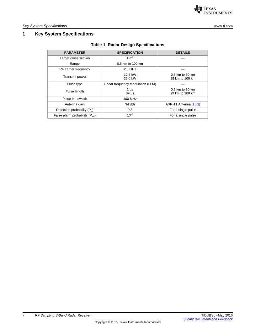
1 Key System Specifications
Table 1. Radar Design Specifications
PARAMETER SPECIFICATION DETAILSTarget cross section 1 m2 —
Range 0.5 km to 100 km —RF carrier frequency 2.8 GHz —
Transmit power 12.5 kW25.0 kW
0.5 km to 30 km29 km to 100 km
Pulse type Linear frequency modulation (LFM) —
Pulse length 1 µs89 µs
0.5 km to 30 km29 km to 100 km
Pulse bandwidth 100 MHz —Antenna gain 34 dBi ASR-11 Antenna [1] [2]
Detection probability (PD) 0.8 For a single pulseFalse alarm probability (PFA) 10–6 For a single pulse

100 km
500 m
www.ti.com System Description
3TIDUBS6–May 2016Submit Documentation Feedback
Copyright © 2016, Texas Instruments Incorporated
RF Sampling S-Band Radar Receiver
2 System DescriptionThe TIDA-00814 reference design shows the use of direct radio frequency (RF) sampling in radar receiverapplications. The focus of this design application is radar operating in S-band (2 GHz to 4 GHz), wheredirect RF sampling is possible using the ADC32RF45, 3-Gsps, 14-bit, dual channel analog-to-digitalconverter (ADC). The 3.3-GHz input bandwidth (BW) of the ADC32RF45 can be stretched to support4 GHz with some allowable attenuation. This reference design has been designed to operate as an airtraffic control radar (airport surveillance radar) similar to the ASR-11 radar currently in operation at thetime of this writing [1] [2]. Figure 1 shows the use case where the radar can detect planes from 500 m to100 km. The design uses two different pulses: one to detect targets near the airport and one to detecttargets far from the airport. The range of these pulses is defined as 0.5 km to 30 km and 29 km to 100 km,respectively.
Figure 1. Airport Air Traffic Control Radar Use Case
The receiver only requires using amplifiers, filters, transformers (or baluns), and the RF samplingADC32RF45 device. This architecture does not require analog mixing stages or local oscillators (LO),thereby reducing the overall component count and size of the solution.
The performance of the receiver is analyzed and then verified through measurement. A matched-quadrature filter detector is used with a simulated radar return signal generated by a digital-to-analogconverter (DAC). Gain or phase equalization is not used in the measurement; however, the addition ofequalization may increase the performance of the receiver. Note that the ASR-11 specifications have beenmodified to fit components that were readily available in the lab for testing.

ADC
Copyright © 2016, Texas Instruments Incorporated
Block Diagram www.ti.com
4 TIDUBS6–May 2016Submit Documentation Feedback
Copyright © 2016, Texas Instruments Incorporated
RF Sampling S-Band Radar Receiver
3 Block DiagramFigure 2 shows the block diagram for the TIDA-00814 reference design. The most obvious benefit of theRF sampling architecture is the low number of components required when comparing to a traditionalheterodyne architecture. The main components that this design uses are two amplifiers, a bandpass filter,an attenuator, transformers, and an ADC32RF45 device. Section 4.6 describes these components in moredetail.
Figure 2. TIDA-00814 Block Diagram
3.1 Highlighted Products
3.1.1 ADC32RF45The essential component for the direct RF sampling radar in the TIDA-00814 design is the ADC32RF45,which is a 14-bit, 3-GSPS ADC. The ADCs low noise floor and high bandwidth enable use of the ADC fordirect RF sampling through L-band and S-band frequency ranges. The ADC has a number of features toimprove direct RF sampling performance and simplify radar architectures.
The ADC32RF45 has a multiband digital-down conversion (DDC) block for each ADC channel. Twoseparate frequency bands can be downconverted simultaneously from the captured signal at the ADCoutput for each ADC channel. This feature enables downconversion of up to four frequencies for a singleADC32RF45 device. The DDC block allows offloading of digital mixing and decimation from the fieldprogrammable gate array (FPGA) while also reducing total data throughput and power consumption of theinterface. Additionally, if the designer uses a single down-converter per ADC channel, the designer canhop the mixing frequency by switching between three independent NCOs per channel. The NCO that isnot selected during this time continues to run so that hopping back to that frequency maintains the phasecoherency.
Figure 3 shows the block diagram for the ADC32RF45. The diagram shows various DDCs as well as theDDC bypass, which can be used to enable the full data rate.

ADCADCADC
ADCADCADC
INAP
SYSREFP
CLKINPPLL
50 �
Buffer
INBP
50 �
BufferDB[0,1]P
DA[0,1]P
DA[2,3]P
DB[2,3]P
GPIO1..4
ADC
Digital Block
InterleaveCorrection
N
N
N
N
NCOCTRL
SYNCBP
0º/180º Clock
JES
D20
4BIn
terf
ace
NCO
FASTDET.
FASTDET.
NCO
NCO
NCO
ADC
Digital Block
InterleaveCorrection
Copyright © 2016, Texas Instruments Incorporated
INAM
SYSREFM
CLKINM
INBM
DB[0,1]M
DA[0,1]M
DA[2,3]M
DB[2,3]M
SYNCBM
www.ti.com Block Diagram
5TIDUBS6–May 2016Submit Documentation Feedback
Copyright © 2016, Texas Instruments Incorporated
RF Sampling S-Band Radar Receiver
Figure 3. ADC32RF45 Block Diagram
t tr e2 2
P GP A
4 R 4 R
s
= ´ ´
p p
TransmissionTime
Dwell Time
Time: 1 µs 100 µs
500 m 30 km
0 µs
0 mRange: Radar Range
Propagation Delay
TransmissionTime
Dwell Time
Time: 89 µs 333 µs
29 km 100 km
0 us
0 mRange: Radar Range
Propagation Delay
(a)
(b)
97 µs
1.7 µs
System Design Theory www.ti.com
6 TIDUBS6–May 2016Submit Documentation Feedback
Copyright © 2016, Texas Instruments Incorporated
RF Sampling S-Band Radar Receiver
4 System Design Theory
4.1 Radar SignalsThe design uses two radar signals based on two ranges to limit the average transmit power. For targetsfrom 500 m to 30 km, a linear frequency modulated (LFM) pulse with a period of 1 µs and transmit powerof 12.5 kW is used. For targets from 29 km to 100 km, an LFM pulse with a period of 89 µs and transmitpower of 25 kW is used. The longer pulse length, in addition to a higher transmit power, increases theenergy of the return signal. The ranges overlap to ensure that there are no dead spots. Table 2 shows thetwo ranges and their respective signal types and pulse lengths.
Table 2. Summary of Radar Transmit Signals for Defined Ranges
RANGE PULSE TYPE TRANSMITPOWER
PULSELENGTH
TRANSMITENERGY
CENTERFREQUENCY
SIGNALBANDWIDTH
500 m to 30 km LFM 12.5 kW 1 µs 0.0125 J 2.8 GHz 100 MHz29 km to 100 km LFM 25 kW 89 µs 2.23 J 2.8 GHz 100 MHz
4.2 Transmit and Dwell TimesFigure 4 shows the transmit time, dead time, dwell times, and associated ranges for the two radar pulses.The minimum distance for each range sets the maximum pulse width. The gray areas in the figure indicatethe dead time during the switch from transmission to receive operation. The propagation delays are basedon the speed of light in free space, which is 3.33 ns/m.
Figure 4. Transmission, Dwell Times, and Ranges for Near (a) and Far (b) Targets
4.3 Radar Range and Receive SignalThe common radar equation can be used to find the total attenuation of the signal to the target and backby using the required range, frequency, transmission power, and antenna gain. Equation 1 shows thebasic form of the radar equation:
(1)

Target Range (km)
Rec
eive
d P
ower
(dB
m)
0.1 0.2 0.3 0.40.5 0.7 1 2 3 4 5 6 7 8 10 20 30 40 50 70 100 200 300 500 700 1000-120
-110
-100
-90
-80
-70
-60
-50
-40
-30
-20
D001D001
Near RangeFar Range
r tP P= a ´
( )
2 2
tr
3 4t
GP
P 4 R
´ s ´ la = =
p ´
( )
2 2
t tr 3 4
P GP
4 R
´ s ´ l=
p ´
2
te
GA
4
´ l=
p
www.ti.com System Design Theory
7TIDUBS6–May 2016Submit Documentation Feedback
Copyright © 2016, Texas Instruments Incorporated
RF Sampling S-Band Radar Receiver
If the designer assumes that the transmit and receive antenna are the same, then the designer canreplace the effective aperture (Ae) by using the relationship between transmit gain and receive effectiveaperture, as in Equation 2:
(2)
(3)
Equation 4 calculates the propagation attenuation, α, where α is defined as a gain and can be defined asPr / Pt. This propagation attenuation provides a relationship between the receive power and transmit powerindependent of the transmit power.
(4)
The returned power of the return pulse is then equal to the following calculation in Equation 5:(5)
Table 3 shows a summary of the minimum and maximum propagation attenuation (α) and received powerfor the defined radar signals and ranges.
Table 3. Propagation Attenuation and Return Signal Power Versus Range
RANGE Pt MAX α MIN α MAX Pr MIN Pr
500 m to 30 km 12.5 kW –92.3 dB –163.5 dB –21.4 dBm –92.5 dBm29 km to 100 km 25 kW –162.9 dB –184.4 dB –88.9 dBm –110.4 dBm
Similarly, the return power can be calculated across the full radar range, as Figure 5 shows.
Figure 5. Received Power vs Radar Range

2
As
r P
2
A
2 r PA
P T
P T
´l =
s
´s =
l
2
2
M A
2
´l =
´ s
( ) ( ) ( )2 2
I Qr n r n r n= +
( ) ( ) ( )M 1
Q Q
k 0
1r n h k n k
M
-
=
= ´ c -å
( ) ( ) ( )M 1
I I
k 0
1r n h k n k
M
-
=
= ´ c -å
'g
ADCx(t)x(n)
HI(z)
HQ(z) ( )2
> �
< �
Detection
No Detection
rI(n)
rQ(n)
r(n)
( )2
Copyright © 2016, Texas Instruments Incorporated
System Design Theory www.ti.com
8 TIDUBS6–May 2016Submit Documentation Feedback
Copyright © 2016, Texas Instruments Incorporated
RF Sampling S-Band Radar Receiver
4.4 Receiver PerformanceAfter calculating the received power at the farthest distance for each signal, the designer can determinethe required noise performance of the receiver. Figure 6 shows a block diagram of the radar receiver.
Figure 6. Radar Receiver Block Diagram
The signal received at the antenna is x(t) and the sampled signal is x(n). The detection scheme uses aquadrature matched filter, where the filters HI(z) and HQ(z) are in-phase and quadrature-phase matchedfilters of transmitted LFM signal, respectively. Each filter has a length of M and amplitude of the squareroot of M. The resulting complex filter has a constant envelope. The output of the filters are defined as rI(n)and rQ(n). The sum of squares of rI(n) and rQ(n), called r(n), is used as the decision signal and comparedagainst a fixed threshold, , to determine whether a target is present. The following Equation 6,Equation 7, and Equation 8 show these relationships:
(6)
(7)
(8)
The specification requires the probability of detecting detection (PD) for a target at 100 km away from theradar for a single pulse to beas 0.8 and a false alarm probability (PFA) of 10-6. The envelope detector,defined as r(n), has a central chi-squared distribution when no target is present and a non-central, chi-squared distribution when a target is present. A look-up table can be used to find the energy-to-noise ratio(ENR) that is required to meet the PD and PFA specifications, which has been found as 35.5 (15.5 dB) forthis system [3]. The ENR, defined below in the following Equation 9 as λ, can then be used to find therequired noise spectral density of the system.
(9)
ENR is a function of the received signal amplitude and the noise variance. Rewriting the ENR in terms ofthe analog, received signal energy and solving for the noise variance results in Equation 10:
where
• represents the required input-referred noise power of the receiver. (10)

( ){ }( )' 2 2
x2
D r 1
2QP P r n ;H
l
æ ö´´ ç ÷ç ÷sè
g= > g =
ø
''
( ){ } 2
FA r 0P P r n ;H e
g
s-
= > g =
'
'
'g
'g
( )
0
1
H
H
r n>
g<
'
[ ]2
N 10 r 10 P
dBm dBmP 10 log P 10 log T ENR dB
Hz 0.001 Hz
sé ù é ù= ´ = + ´ -ê ú ê úë û ë û
2
As
www.ti.com System Design Theory
9TIDUBS6–May 2016Submit Documentation Feedback
Copyright © 2016, Texas Instruments Incorporated
RF Sampling S-Band Radar Receiver
can then be calculated in terms of dBm/Hz (see Equation 11). Table 4 summarizes the results for themaximum ranges for each signal (near and far) and the required noise figure (NF) is calculated assuming–174 dBm/Hz as the input signal noise spectral density.
(11)
Table 4. Required Input Referred Noise Floor and Noise Figure for Worst-Case Ranges
RANGE Pt TP Pr [dBm] REQUIRED PN[dBm/Hz] MAXIMUM NF [dB]
30 km 12.5 kW 1 µs –92.5 dBm –168 6100 km 25 kW 89 µs –110.4 dBm –166.4 7.6
Because the 30-km range has a stricter noise figure requirement, this specification sets the noise figurerequirement for the receiver.
4.5 Detection ThresholdFind the detection rule based on the probability distribution functions of r(n) for a target being present anda target not being present at each time point, n, which is defined as events H1 and H0, respectively. Thedecision rule is compactly defined as shown in Equation 12:
where
• The threshold, , is defined by a likelihood ratio test, using the Neyman-Pearson lemma [3] (12)
The resulting false alarm probability and detection probability for a single pulse have been defined in thefollowing Equation 13 and Equation 14 in terms of the threshold, .
(13)
(14)

ADC
Copyright © 2016, Texas Instruments Incorporated
G = 16.44 dBNF = 3.0 dBIIP3 = 25.6 dBm
G = 16.44 dBNF = 3.0 dBIIP3 = 25.6 dBm
G = t0.34 dBNF = 0.34 dB
G = ±1.2 dBNF = 1.2 dB
G = 0 dBNF = 25.6 dBIIP3 = 29 dBm
Totals:G = 26.49 dBNF = 4.53 dBIIP3 = 1.64 dBm
G = t3 dBNF = 3 dB
G = t1.85 dBNF = 1.85 dB
( ) 1
2M| H
AE r n
4é ù @ë û
( )
2
0
Q2
1
N 0, given H2
r nMA
N , given H2 2
ì æ ösï ç ÷ç ÷ï è øí
æ ösïç ÷ï ç ÷è øî
:
( )
2
0
I2
1
N 0, given H2
r nMA
N , given H2 2
ì æ ösï ç ÷ç ÷ï è øí
æ ösïç ÷ï ç ÷è øî
:
System Design Theory www.ti.com
10 TIDUBS6–May 2016Submit Documentation Feedback
Copyright © 2016, Texas Instruments Incorporated
RF Sampling S-Band Radar Receiver
The noise variance for the threshold calculation can be determined as the variance of the output of one ofthe I or Q matched filters given in Equation 6 and Equation 7 when no target is present. Equation 15 andEquation 16 provide the distributions for rI(n) and rQ(n) for reference:
(15)
(16)
Equation 17 calculates the expected value of r(n) when a target is present, which can then be used to findthe amplitude of the received signal. The approximation assumes that the signal energy is much greaterthan the noise variance.
(17)
4.6 Receiver DesignBased on the results in the previous subsection, a receiver lineup has been designed and measured in thelab to meet the required noise figure. Note that the third order intercept point (IIP3) has been ignoredwhen generating the receiver requirements; however, this value has been calculated in the followingFigure 7 for reference.
Figure 7. Lineup Analysis for Receiver Used in Lab Measurements
The designed receiver consists of two RF amplifiers, an attenuator, a bandpass filter, two transformers,and an ADC32RF45 device. The amplifiers are Mini-Circuits ZRL-3500+ amplifiers and were readilyavailable in the lab. The bandpass filter is a tunable filter with a bandwidth of approximately 100 MHz thatremoves wideband noise and interferers from the antenna and amplifiers. The attenuator is placed at theinput to the ADC32RF45 EVM to reduce the overall gain, increase the IIP3, and improve the return loss(S11) of the EVM, but does result in an increase in the total noise figure. The gain is set such thatsaturation does not occur for a target at the closest range of 500 m. The two transformers provide single-ended to differential conversion with a good differential balance. The transformers on the ADC32RF45EVM were replaced with Mini-Circuits TC1-1-43A+ because these transformers perform better at thereceiver operating frequencies. The attenuator shown at the input of the ADC acts as a model for thebandwidth rolloff at the operating frequencies and was inferred from the total receiver gain, but aligns wellwith bandwidth measurements.
The gains in the lineup are based on measurements, but align with the data found in the respectivedatasheets. The noise figures used in the calculations are from datasheets, except for lossy elementswhere the noise figure is equal to the loss.
FPGA or DSPADC32RF45DDC Bypass Mode
ADC
HI(z)
HQ(z)
( )2
( )2
> �
< �
Detection
No Detection
rI(n)
rQ(n)
r(n)cos(2�FCn/FS)
sin(2�FCn/FS)
8
JESD204BFour lanes at 12 Gbps
8
Copyright © 2016, Texas Instruments Incorporated
ADC
Copyright © 2016, Texas Instruments Incorporated
G = 19 dBNF = 1.0 dBIIP3 = 21 dBm
G = 15 dBNF = 2.0 dBIIP3 = 45 dBm
G = t0.34 dBNF = 0.34 dB
G = ±1.2 dBNF = 1.2 dB
G = 0 dBNF = 25.6 dBIIP3 = 29 dBm
Totals:G = 30.61 dBNF = 1.99 dBIIP3 = 1.87 dBm
G = 0 dBNF = 0 dB
G = t1.85 dBNF = 1.85 dB
www.ti.com System Design Theory
11TIDUBS6–May 2016Submit Documentation Feedback
Copyright © 2016, Texas Instruments Incorporated
RF Sampling S-Band Radar Receiver
4.7 Design ExtensionsThe following subsections describe a few extensions to this reference design.
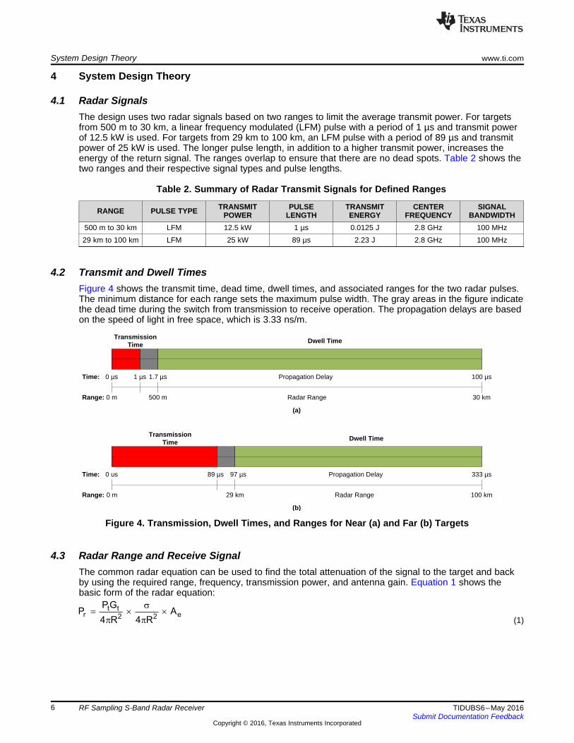
4.7.1 PerformanceThe specifications for this reference design have been mainly designed around hardware that was readilyavailable in the lab. Most real-world receivers require lower noise figures, around 2 dB or less. Thisperformance is certainly achievable using this receiver architecture by properly choosing the front endLNA and total receiver gain. Figure 8 shows an example lineup that achieves a 2-dB noise figure. A lowernoise figure in the first low noise amplifier (LNA) and a higher overall gain optimizes the receiver for abetter noise figure. The second amplifier is a linear amplifier with an additional drive capability to directlydrive the ADC32RF45 device.
Figure 8. Example Lineup for 2-dB Receiver Noise Figure
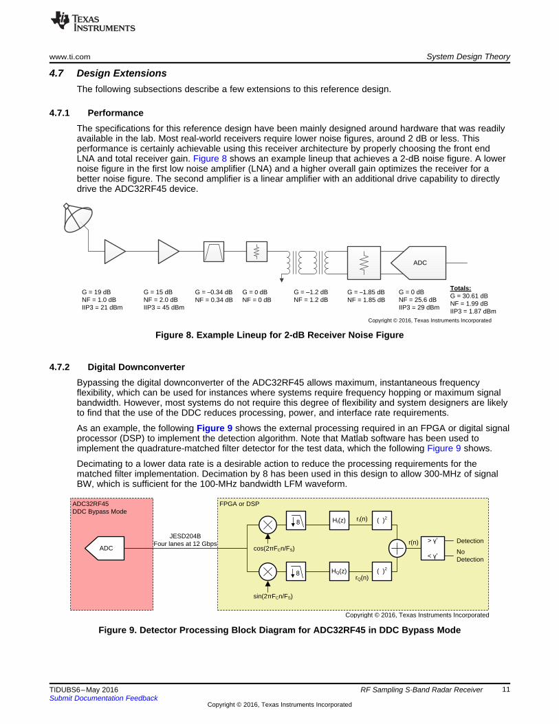
4.7.2 Digital DownconverterBypassing the digital downconverter of the ADC32RF45 allows maximum, instantaneous frequencyflexibility, which can be used for instances where systems require frequency hopping or maximum signalbandwidth. However, most systems do not require this degree of flexibility and system designers are likelyto find that the use of the DDC reduces processing, power, and interface rate requirements.
As an example, the following Figure 9 shows the external processing required in an FPGA or digital signalprocessor (DSP) to implement the detection algorithm. Note that Matlab software has been used toimplement the quadrature-matched filter detector for the test data, which the following Figure 9 shows.
Decimating to a lower data rate is a desirable action to reduce the processing requirements for thematched filter implementation. Decimation by 8 has been used in this design to allow 300-MHz of signalBW, which is sufficient for the 100-MHz bandwidth LFM waveform.
Figure 9. Detector Processing Block Diagram for ADC32RF45 in DDC Bypass Mode

Copyright © 2016, Texas Instruments Incorporated
FPGA or DSPADC32RF45Decimate-by-8 Mode
ADC> �
< �
Detection
No Detection
rI(n)
rQ(n)
r(n)cos(2�FCn/FS)
sin(2�FCn/FS)
8
8
JESD204BTwo lanes at 7.5 Gbps
HI(z)
HQ(z)
( )2
( )2
System Design Theory www.ti.com
12 TIDUBS6–May 2016Submit Documentation Feedback
Copyright © 2016, Texas Instruments Incorporated
RF Sampling S-Band Radar Receiver
An alternative approach to that shown in Figure 9 is to make use of the DDC inside of the ADC32RF45device to off-load processing from the FPGA or DSP to reduce the resource requirements. Additionally,when using this alternative approach, the interface rate is significantly reduced. Instead of four serdeslanes at 12 Gbps, for a total throughput of 48 Gbps, the DDC enables reduction to two lanes at 7.5 Gbps,for a total throughput of 15 Gbps, which is a 68.75% reduction of the data rate and has an associatedreduction in interface power consumption. The FPGA or DSP now just implements the quadrature-matched filter and detection rule (see Figure 10).
Figure 10. Detector Processing Block Diagram for ADC32RF45 in Decimate-by-8 Mode
The ADC32RF45 DDCs also have the ability to perform phase-coherent frequency hopping. Threenumerically controlled oscillators (NCOs) are available per ADC channel. Each NCO can be set to adifferent operating frequency and run independently from the others. The desired frequency band isselected by choosing the appropriate NCO using the input pins of the device. The other NCOs continue torun to while a different NCO is selected to maintain the continuous phase.
RF Source3 GHz, 17 dBm
Power Splitter
Jumper set to EXT_CLK
Fc = 3 GHz
Copyright © 2016, Texas Instruments Incorporated
RF DAC
Fc = 2.8 GHzBW = 100 MHz
ZRL-3500+ ZRL-3500+ 3-dB Attenuator
www.ti.com Getting Started Hardware
13TIDUBS6–May 2016Submit Documentation Feedback
Copyright © 2016, Texas Instruments Incorporated
RF Sampling S-Band Radar Receiver
5 Getting Started Hardware
5.1 ADC32RF45 EVMSee the ADC32RF45 EVM tool folder at http://www.ti.com/tool/adc32rf45evm.
5.2 TSW14J56 EVMSee the TSW14J56 EVM tool folder at http://www.ti.com/tool/tsw14j56evm.
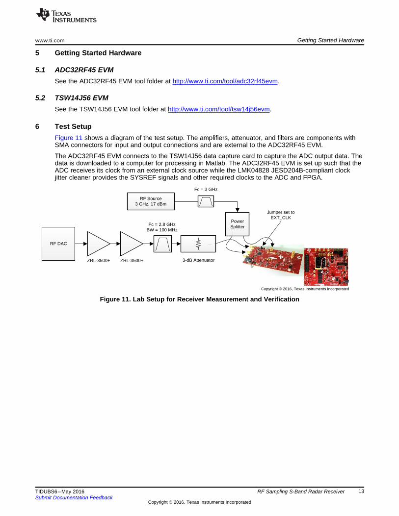
6 Test SetupFigure 11 shows a diagram of the test setup. The amplifiers, attenuator, and filters are components withSMA connectors for input and output connections and are external to the ADC32RF45 EVM.
The ADC32RF45 EVM connects to the TSW14J56 data capture card to capture the ADC output data. Thedata is downloaded to a computer for processing in Matlab. The ADC32RF45 EVM is set up such that theADC receives its clock from an external clock source while the LMK04828 JESD204B-compliant clockjitter cleaner provides the SYSREF signals and other required clocks to the ADC and FPGA.
Figure 11. Lab Setup for Receiver Measurement and Verification

Test Data www.ti.com
14 TIDUBS6–May 2016Submit Documentation Feedback
Copyright © 2016, Texas Instruments Incorporated
RF Sampling S-Band Radar Receiver
7 Test DataThis section contains a selection of measurements to verify performance and show application levelresults. Section 7.1 shows the gain and noise figure measurements. Section 7.2 shows the results of thematched filter output for simulated return signals.
7.1 Gain and Noise Figure VerificationThe gain of the RF front end, from the input to the filter output, was measured using a network analyzer.Additionally, the filter was measured separately. The total gain was then measured using single tonesplaced across the band and by using the knowledge that the ADC32RF45 full-scale power is 6.59 dBm.The input power was measured using a spectrum analyzer before being applied to the receiver. Table 5summarizes the results.
Table 5. Summary of Receiver Gain and Flatness
FREQUENCY(MHz)
INPUT POWER(dBm)
ADC OUTPUT POWER(dBFS)
ADC OUTPUT POWER(dBm) GAIN (dB) RIPPLE (dB)
2750 –62.95 –42.52 –35.93 27.02 0.532775 –63.16 –42.46 –35.87 27.29 0.82800 –63.1 –43.2 –36.61 26.49 0 (Reference)2825 –62.88 –43.12 –36.53 26.35 –0.142850 –63.08 –43.96 –37.37 25.71 –0.78
Figure 12. RF Front-End Gain Measurement (S21)

www.ti.com Test Data
15TIDUBS6–May 2016Submit Documentation Feedback
Copyright © 2016, Texas Instruments Incorporated
RF Sampling S-Band Radar Receiver
Figure 13. Filter Response Measurement (S21)
Determine the noise figure by measuring the noise of the receiver at the ADC output, subtracting themeasured gain of the receiver, and finding the difference between the calculated input-referred noise andthe thermal noise floor of –174 dBm/Hz. The plot in Figure 14 shows the output noise measurements andTable 6 shows the results and calculated noise figures. The noise figure measurements align well with thecalculated noise figure of 4.53 dB. Figure 15 shows a measurement of the ADC noise floor with aterminated input for reference and is used to determine the noise figure of the ADC for the lineup analysis.
Figure 14. Receiver Noise Floor Measured at ADC Output

Test Data www.ti.com
16 TIDUBS6–May 2016Submit Documentation Feedback
Copyright © 2016, Texas Instruments Incorporated
RF Sampling S-Band Radar Receiver
Figure 15. Noise Floor of 50-Ω Terminated ADC Without Receiver Front End
Table 6. Receiver Noise Measurements and Noise Figure Calculations
MEAS.FREQUENCY
(MHz)MEAS. BW
(MHz)
MEAS.OUTPUTNOISE(dBFS)
MEAS.OUTPUTNOISE
(dBFS/Hz)
MEAS.OUTPUTNOISE
(dBm/Hz)RX GAIN (dB)
INPUT REF.NOISE
(dBm/Hz)NOISE
FIGURE (dB)
2750 5 –82.70 –149.69 –143.10 27.02 –170.12 3.882775 5 –82.24 –149.23 –142.64 27.29 –169.93 4.072800 5 –82.80 –149.79 –143.20 26.49 –169.69 4.312825 5 –82.88 –149.87 –143.28 26.35 –169.63 4.372850 5 –83.33 –150.32 –143.73 25.71 –169.44 4.56

( ) ( )' 2 6
FAln P 3.439 ln 10 47.5-g = - s ´ = - ´ =
'g
www.ti.com Test Data
17TIDUBS6–May 2016Submit Documentation Feedback
Copyright © 2016, Texas Instruments Incorporated
RF Sampling S-Band Radar Receiver
7.2 Calculation of Detection Threshold
Determine the detection rule threshold, , by measuring the variance of the output of one of the matchedfilters, either HI(z) or HQ(z), when no signal is present. Figure 16 shows the output of the in-phase filter,rI(n), and gives the calculated variance of the matched filter output. Note that the variance is measuredbefore the output is squared.
Figure 16. Matched Filter Output Noise for Detection Threshold Calculation
The PFA equation (see preceding Equation 13) can then be used to solve for the appropriate threshold fora given noise variance, as the following Equation 18 shows. The detection probability has already beenaccounted for by determining the ENR from the look-up table.
(18)
7.3 Radar Return Signal MeasurementsThe radar return signals for the minimum and maximum ranges were created using a DAC to simulate areturn signal, as shown in the following Figure 17, Figure 18, Figure 19, and Figure 20. The power of thereturn signals were calculated in Section 4.3. The signal in the figure is the output of the quadraturematched filter, r(n). Each figure has two peaks, the first is a reference peak that represents the pulsetransmission and is not to scale. The second peak is the return signal at the expected return signal power.The red line represents the detection threshold. Table 7 and Table 8 summarize the results.

Test Data www.ti.com
18 TIDUBS6–May 2016Submit Documentation Feedback
Copyright © 2016, Texas Instruments Incorporated
RF Sampling S-Band Radar Receiver
Figure 17. 500-m, 12.5-kW Transmit Power, 1-µs LFM Pulse
Figure 18. 30-km, 12.5-kW Transmit Power, 1-µs LFM Pulse

www.ti.com Test Data
19TIDUBS6–May 2016Submit Documentation Feedback
Copyright © 2016, Texas Instruments Incorporated
RF Sampling S-Band Radar Receiver
Figure 19. 29-km, 25-kW Transmit Power, 89-µs LFM Pulse
Figure 20. TIDUBS63051
Table 7. Summary of Return Time for Radar Return Signal Measurements
RANGE(km)
TRANSMITPOWER (kW)
PULSELENGTH (µs)
REFERENCE TIME(µs)
RETURN TIME(µs)
MEASUREDRETURN TIME (µs)
CALCULATEDRANGE (km)
0.5 12.5 1 430.48 433.81333 3.33333 0.499999530 12.5 1 339.4 539.4 200.00 30.00029 25 89 549.78933 743.12267 193.33334 29.000001100 25 89 197.6 864.3 666.7 100.005

Test Data www.ti.com
20 TIDUBS6–May 2016Submit Documentation Feedback
Copyright © 2016, Texas Instruments Incorporated
RF Sampling S-Band Radar Receiver
Table 8. Summary of Return Power for Radar Return Signal Measurements
RANGE(km)
TRANSMITPOWER (kW)
PULSELENGTH (µs)
MATCHED FILTEROUTPUT r(n)
CALCULATEDAMPLITUDE (LSBs)
CALCULATEDRECEIVE
POWER (dBm)
EXPECTEDRECEIVE
POWER (dBm)0.5 12.5 1 2.3427509x10⁹ 1767.4 –21.18 –21.430 12.5 1 114.6 0.391 –94.29 –92.529 25 89 33875.786 0.712 –89.08 –88.9100 25 89 318.8 0.069 –109.34 –110.4
Figure 21 shows a zoomed-in view of the return pulse from the 100-km measurement (from Figure 20).The pulse is narrow because of pulse compression from the long pulse length and the 100-MHzbandwidth LFM waveform. The narrow output pulse allows the radar to have better spatial resolution todetect nearby targets. The time-bandwidth product of the 89-µs pulse is 8900, whereas the time-bandwidth product of the 1-µs pulse is 100.
Figure 21. Return Signal From 100-km Return Measurement

www.ti.com Design Files
21TIDUBS6–May 2016Submit Documentation Feedback
Copyright © 2016, Texas Instruments Incorporated
RF Sampling S-Band Radar Receiver
8 Design Files
8.1 SchematicsTo download the schematics, see the design files at TIDA-00814.
8.2 Bill of MaterialsTo download the bill of materials (BOM), see the design files at TIDA-00814.
8.3 Altium ProjectTo download the Altium project files, see the design files at TIDA-00814.
8.4 Gerber FilesTo download the Gerber files, see the design files at TIDA-00814.
8.5 Assembly DrawingsTo download the assembly drawings, see the design files at TIDA-00814.
9 Software FilesTo download the software files, see the design files at TIDA-00814.
10 References
1. NTIA, Analysis and Resolution of RF Interference to Radars Operating in the Band 2700-2900 MHzfrom Broadband Communication Transmitters, NTIA Report TR-13-490, Oct 2012
2. U.S. Department of Transportation, Airport Surveillance Radar Model 11 (ASR-11) FAA Test andEvaluation Master Plan (TEMP), U.S. Dept of Transportation Report DOT/FAA/CT-TN97/27, Feb 1998
3. Kay, Steven M.; Fundamentals of Statistical Signal Processing, Volume II: Detection Theory, 1st Ed;1998
4. Skolnik, Merrill; Radar Handbook, 3rd Ed; 2008
11 About the AuthorMATTHEW GUIBORD is a systems engineer in TI’s high-speed data converters group. His focus is onaerospace and defense and test and measurement systems. Matt received his bachelor’s degree fromMichigan State University, East Lansing, Michigan.

IMPORTANT NOTICE FOR TI REFERENCE DESIGNS
Texas Instruments Incorporated (‘TI”) reference designs are solely intended to assist designers (“Designer(s)”) who are developing systemsthat incorporate TI products. TI has not conducted any testing other than that specifically described in the published documentation for aparticular reference design.TI’s provision of reference designs and any other technical, applications or design advice, quality characterization, reliability data or otherinformation or services does not expand or otherwise alter TI’s applicable published warranties or warranty disclaimers for TI products, andno additional obligations or liabilities arise from TI providing such reference designs or other items.TI reserves the right to make corrections, enhancements, improvements and other changes to its reference designs and other items.Designer understands and agrees that Designer remains responsible for using its independent analysis, evaluation and judgment indesigning Designer’s systems and products, and has full and exclusive responsibility to assure the safety of its products and compliance ofits products (and of all TI products used in or for such Designer’s products) with all applicable regulations, laws and other applicablerequirements. Designer represents that, with respect to its applications, it has all the necessary expertise to create and implementsafeguards that (1) anticipate dangerous consequences of failures, (2) monitor failures and their consequences, and (3) lessen thelikelihood of failures that might cause harm and take appropriate actions. Designer agrees that prior to using or distributing any systemsthat include TI products, Designer will thoroughly test such systems and the functionality of such TI products as used in such systems.Designer may not use any TI products in life-critical medical equipment unless authorized officers of the parties have executed a specialcontract specifically governing such use. Life-critical medical equipment is medical equipment where failure of such equipment would causeserious bodily injury or death (e.g., life support, pacemakers, defibrillators, heart pumps, neurostimulators, and implantables). Suchequipment includes, without limitation, all medical devices identified by the U.S. Food and Drug Administration as Class III devices andequivalent classifications outside the U.S.Designers are authorized to use, copy and modify any individual TI reference design only in connection with the development of endproducts that include the TI product(s) identified in that reference design. HOWEVER, NO OTHER LICENSE, EXPRESS OR IMPLIED, BYESTOPPEL OR OTHERWISE TO ANY OTHER TI INTELLECTUAL PROPERTY RIGHT, AND NO LICENSE TO ANY TECHNOLOGY ORINTELLECTUAL PROPERTY RIGHT OF TI OR ANY THIRD PARTY IS GRANTED HEREIN, including but not limited to any patent right,copyright, mask work right, or other intellectual property right relating to any combination, machine, or process in which TI products orservices are used. Information published by TI regarding third-party products or services does not constitute a license to use such productsor services, or a warranty or endorsement thereof. Use of the reference design or other items described above may require a license from athird party under the patents or other intellectual property of the third party, or a license from TI under the patents or other intellectualproperty of TI.TI REFERENCE DESIGNS AND OTHER ITEMS DESCRIBED ABOVE ARE PROVIDED “AS IS” AND WITH ALL FAULTS. TI DISCLAIMSALL OTHER WARRANTIES OR REPRESENTATIONS, EXPRESS OR IMPLIED, REGARDING THE REFERENCE DESIGNS OR USE OFTHE REFERENCE DESIGNS, INCLUDING BUT NOT LIMITED TO ACCURACY OR COMPLETENESS, TITLE, ANY EPIDEMIC FAILUREWARRANTY AND ANY IMPLIED WARRANTIES OF MERCHANTABILITY, FITNESS FOR A PARTICULAR PURPOSE, AND NON-INFRINGEMENT OF ANY THIRD PARTY INTELLECTUAL PROPERTY RIGHTS.TI SHALL NOT BE LIABLE FOR AND SHALL NOT DEFEND OR INDEMNIFY DESIGNERS AGAINST ANY CLAIM, INCLUDING BUT NOTLIMITED TO ANY INFRINGEMENT CLAIM THAT RELATES TO OR IS BASED ON ANY COMBINATION OF PRODUCTS ASDESCRIBED IN A TI REFERENCE DESIGN OR OTHERWISE. IN NO EVENT SHALL TI BE LIABLE FOR ANY ACTUAL, DIRECT,SPECIAL, COLLATERAL, INDIRECT, PUNITIVE, INCIDENTAL, CONSEQUENTIAL OR EXEMPLARY DAMAGES IN CONNECTION WITHOR ARISING OUT OF THE REFERENCE DESIGNS OR USE OF THE REFERENCE DESIGNS, AND REGARDLESS OF WHETHER TIHAS BEEN ADVISED OF THE POSSIBILITY OF SUCH DAMAGES.TI’s standard terms of sale for semiconductor products (http://www.ti.com/sc/docs/stdterms.htm) apply to the sale of packaged integratedcircuit products. Additional terms may apply to the use or sale of other types of TI products and services.Designer will fully indemnify TI and its representatives against any damages, costs, losses, and/or liabilities arising out of Designer’s non-compliance with the terms and provisions of this Notice.IMPORTANT NOTICE
Mailing Address: Texas Instruments, Post Office Box 655303, Dallas, Texas 75265Copyright © 2016, Texas Instruments Incorporated