Embed Size (px)
Citation preview

Lab 1 in SMD152 Jonas Thor September 2003
An Introduction to VHDL Based Design
for Xilinx FPGAs

1
1 Introduction The purpose of this lab is to give a first introduction to the VHDL based design flow for Xilinx FPGAs. The entire VHDL source is given to you, but it is highly recommended that you study the code and make sure that you understand the main concepts. Note that you can only learn a subset of the tools in this first tutorial-based lab. As you work through future labs, it is expected that you learn the tools by experimenting with the features/options. When you run into problems, or have any questions, please ask for help. However it is usually a good idea to study the extensive online documentation. You should under no circumstances try to contact technical support for any software or hardware used during the course. 1.1 The design flow For design entry Emacs will be used. Simulation will be performed with Cadence NC VHDL and the design will be synthesized with Synplify Pro. The Xilinx ISE software will be used for design implementation. The design flow is illustrated in figure 1.
Design entry Traditionally, design entry has been performed using schematic entry tools. As designs become more complex Hardware Description Languages (HDL), such as VHDL and Verilog, have been adopted. HDLs allows designers to describe hardware using abstract programming. For beginners it might be a bit hard to understand VHDL and how the hardware is created from the code. One recommendation is to “think hardware” when you write your VHDL code. It is not true that when you know VHDL that you are also know digital design. You should regard VHDL as a “tool” to simplify the design work - you have to understand VHDL and digital design. VHDL is a complex and feature rich language. During this course you will, mostly on your own, only learn a subset of the language. VHDL was initially a language for describing the function and structure of digital systems, not for synthesis. That is the reason why only a subset of VHDL is synthesizable. So for logic synthesis you do not have to understand the complete VHDL. In the labs you will use Emacs to write your VHDL code. However if you prefer any other text editor, you may use that.

2
Figure 1. Design Flow
Functional simulation Functional simulation verifies that your VHDL model behaves as expected. At this stage you have no timing information about your design. That is, you do not know the delays of the combinational logic and wires. Do not try to model delays in VHDL that is written for synthesis. The timing information will come from your technology library once the design is implemented.
Design EntryEmacs
Functional Simulation NC
VHDL
SynthesisSynplifyConstraints
Translate (NGDBuild
Map
Place and Route
Static timing analysis
VHDL code
EDIF netlist
Back annotation
Timing Simulation NC VHDL
Configuration
Xilinx ISE

3
Synthesis Synthesis may be defined as constructing a target technology specific netlist from a model of a circuit described in VHDL, or any other HDL. In the Synplify manual we find this description of synthesis: “Although commonly called logic synthesis, or just synthesis, there are several steps going on behind the scenes in a synthesis tool program. The first step is language synthesis (HDL compilation) in which the design you described at a high level of abstraction is compiled to known structural elements. The second step is optimization, in which algorithms make your design as small as possible and run faster. Synplify can perform optimizations with no knowledge of the target technology, while the remainder of the optimizations are performed during the final step. The final step is technology mapping in which the synthesis tool maps your design, using architecture-specific techniques. A design netlist is then generated in a format readable by your programmable logic vendor’s place and route tool.”
Design implementation The netlist generated by the synthesis tool is the input to the ISE Alliance tools. Translation Converts the netlist into a tool specific binary format.
Mapping Assigns a design’s logic elements to the specific physical elements, such as
CLBs and IOBs, that actually implement logic functions in a device.
Placing Assigns design blocks created during mapping to specific locations in the FPGA.
Routing Assigns the interconnect paths in the FPGA.
Static timing analysis
Analysis of delays in the implemented design. Determines if the timing constraints have been met.
Bitstream generation
Converts a design to a bitstream that may be used to configure the FPGA.
Back annotation The implemented design is converted to a VHDL netlist and the net delays are extracted to a Standard Delay Format (SDF) file.
Timing simulation The timing simulation is performed to verify that the function is correct and that there are no timing violations in the implemented design. A structural VHDL netlist and a SDF file is loaded in NC VHDL and the same simulation may be performed as was performed prior to synthesis. For a fully synchronous design the static timing analysis should cover all timing constraints, but a static timing analysis does not verify the functionality.

4
The design The design in this first lab is very simple. Although you may not have seen VHDL code before it should be easy to understand the code below. library ieee; use ieee.std_logic_1164.all; entity Lab1 is port ( Sw1, Sw2, Sw3, Sw4 : in std_logic; -- Switches Bar1, Bar2, Bar3, Bar4 : out std_logic); -- Bar leds end Lab1; architecture combinational of Lab1 is begin B1 : Bar1 <= (Sw1 and Sw2) or (Sw3 and Sw4); B2 : Bar2 <= (Sw1 or Sw2) and (Sw3 or Sw4); B3 : Bar3 <= not Sw1; B4 : Bar4 <= '1' when (Sw1 = Sw2) else '0'; end combinational; The VHDL code describes a purely combinational circuit with 4 inputs and 4 outputs. The push buttons control the outputs – the bar graph LEDs. The combinational logic functions described in the VHDL source will be implemented in the FPGA. The purpose of this lab is to introduce the complete design flow from VHDL modeling to actually testing the design on our lab boards. The lab board, XSB-300E, is shown in the figure below.
THIS IS A PICTURE OF THE OLD BOARD
THIS IS A PICTURE OF THE OLD BOARD.
Dip-switches Bar graph
LEDs
FPGA

5
2 Getting the design files Copy all the files found in /digcad/smd152/lab/1/flowtut to a local directory. 3 Functional simulation You will now use NC VHDL to verify that the design is functionally correct. The following Cadence tools will be used. ncvhdl Compiles a VHDL design ncelab Elaborates the design ncsim Simulates the design What actually takes place during compilation, elaboration and simulation will be further explained in upcoming lectures. Online documentation for the Cadence tools is available with the command cdsdoc 3.1 Preparing your simulation environment With a text editor you will manually create two setup files needed by the simulation tools.
• Library mapping file (cds.lib) - Defines a logical name for the location of your design libraries and associates them with physical directory names.
• Variables file (hdl.var) - Defines variables that affect the behavior of simulation tools and utilities.
The files should be saved in the same directory as you keep you VHDL files. The contents of the cds.lib file must be define worklib ./worklib include $CDS_INST_DIR/tools/inca/files/cds.lib and the contents of the hdl.var must be define WORK worklib include $CDS_INST_DIR/tools/inca/files/hdl.var Create the physical directory worklib with the command mkdir worklib 3.2 Compiling the code Here we will use the command line to compile the VHDL code. You may also compile the code in Emacs. Emacs has a powerful VHDL mode, which I highly recommend that you use. In order to setup Emacs VHDL mode - open a VHDL file and locate the VHDL menu. In that menu select Options Compiler Selected Compiler at Startup Cadence NC. You have been provided with two VHDL files, Lab1.vhd and Lab1_tb.vhd. The first file is the previously listed design file. The other file is the testbench, listed below, that will be used in the simulator to verify that the design behaves as expected. Note that there is one intentional error in the testbench.

6
library ieee; use ieee.std_logic_1164.all; entity Lab1_tb is end Lab1_tb; architecture sim of Lab1_tb is component Lab1 port ( Sw1, Sw2, Sw3, Sw4 : in std_logic; Bar1, Bar2, Bar3, Bar4 : out std_logic); end component; signal Sw1, Sw2, Sw3, Sw4 : std_logic := '0'; signal Bar1, Bar2, Bar3, Bar4 : std_logic; begin -- Instance of Unit Under Test UUT: Lab1 port map ( Sw1 => Sw1, Sw2 => Sw2, Sw3 => Sw3, Sw4 => Sw4, Bar1 => Bar1, Bar2 => Bar2, Bar3 => Bar3, Bar4 => Bar4); Sw1 <= not Sw1 after 10 ns; Sw2 <= not Sw2 after 20 ns; Sw3 <= not Sw3 after 40 ns; Sw <= not Sw4 after 80 ns; assert not (Sw1='1' and Sw2='1' and Sw3 = '1' and Sw4 = '1') report "All posible inputs are tested" severity note; end sim; Now compile the VHDL code with the command ncvhdl -linedebug -messages Lab1.vhd Lab1_tb.vhd The linedebug switch enables line debug capabilities, break points etc. Usually you want to use this switch, but without it simulation will run faster. The message switch simply prints more verbose information to the standard output. You should see the following messages after compiling the code.
This error message is rather self explanatory but sooner or later you will find some error message that you will not understand. To help you better understand cryptic error messages there is another command line tool called nchelp. Run this tool and examine its output. A closely related tool is NCBrowse. Invoke NCBrowse by typing (guess what?) ncbrowse. Choose File Open Logfile… and select the file ncvhdl.log. In the Messages: list, select
7
the single error message. You should now see
The error here is a simple misspelling that the signal named Sw4. Open the file Lab1_tb.vhd in Emacs and correct the error (write Sw4 instead of Sw). Next exit Emacs and recompile the VHDL files. 3.3 Elaborating the design After the VHDL code is compiled the design to be simulated must be elaborated. For now consider elaboration as something you can compare with linking in the “software world”. We will talk about this more in later lectures. Elaborate the top level for simulation which is worklib.lab1_tb:sim. The naming convention is <library name>.<entity name>:<architecture name>. ncelab –messages work.lab1_tb:sim 3.4 Simulating the design Invoke the simulator with the command: ncsim –gui work.lab1_tb:sim You will now see:

8
Now follow the three steps indicated in the figure below: Select UUT, select all inputs and outputs. Click on the waveform icon and the Waveform view should be displayed.
Simulator console. Here messages are displayed and commands are given
Design Browser

9
Now, in any simulator window, select Windows New Source Browser. You should see:
Insert brake here!
1. Select UUT
3. Click the Waveform icon
2. Select all inputs and outputs
10
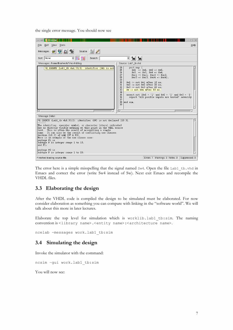
Right click on the line number 31 in the test bench source code. In the pop-up menu select Break at Line. The break should be indicated by a red “dot”.
Now we will start the simulation. In the Simulator console window type the command:
The simulator will now run for 30 ns or until a break is reached. Here the simulator will halt at the brake point at time 0 ns. Give the same command again. You should see:
Now examine the Waveform window. It should look something like this:
Note that in the picture above the inputs and outputs have been grouped. Right click on signals and in the pop-up menu select Create Group.

11
Now remove the brake in the code. Locate the Source Browser window and right click at the break point and select Delete Break. Now give the commands “reset” and “run 200 ns” in the console window. The first command resets the simulation to simulation time 0 ns. The following should have been logged in the console window.
Now, take some time to experiment with the simulator. For instance, in the source code window right click on any signal name. Select “Break on Change”. Now run the simulator using the GUI or giving commands. This was a very short tutorial for the Cadence NC tools. The documentation for the tools spans thousands of pages. To access the documentation issue the command cdsdoc, which will bring up the documentation navigator.
4 Synthesis Start Synplify PRO with the command synplify_pro to bring the Synplify PRO window:

12
Select File New and select Project File as indicated in the dialog box below.
Click OK. Next click the Add File… button in the main Synplify window. Locate the Lab1.vhd file and select that to add it to the project. Next click Impl options… button and select the device options as indicated below.

13
Select the Device options so that they match the FPGA we have on our lab boards as indicated above. Leave all other options to their default values. Click OK. Now is a good time to save the project! Select File Save As… and save the project as lab1.prj. Now select Run Compile Only or press F7. Next click the View Log button. Examine the compilation log – there should be no errors.
Click the icon to display the RTL view. The RTL view is described in the Synplify manual as: “The RTL view displays your design as a high-level, technology-independent schematic. At this high level of abstraction, the design is represented with technology-independent components like variable-width adders, registers, large muxes, state machines, and so on. This view corresponds to the .srs netlist file generated by the software in the Synplicity proprietary format.” Examine the RTL view and compare it to the VHDL code! In the RTL view, double-click the indicated OR-gate. This should bring up the VHDL code that models the OR-gate, as shown in the source code listing below. This function is called cross probing. Cross probing is also available from the source code to the schematic views.

14
Now switch to the main project window in Synplify. Select Run Synthesize or press F8. After a few seconds the design is now mapped to the target technology. Click the Technology
view icon . The Synplify manual states: “The Technology view contains technology-specific primitives. It shows low-level vendor-specific components such as look-up tables, cascade and carry chains, muxes, and flip-flops, which can vary with the vendor and the technology. This view corresponds to the .srm netlist file, generated by the software in the Synplicity proprietary format.” The Xilinx FPGAs does not implement logic functions with gates. Instead the functions are implemented with Look-Up Tables (LUTs). This is visible in technology view:
Double-click OR gate!
Infers the OR-“gate”

15
The LUTs in the technology view are the grey boxes. The gates inside the boxes indicate what function is implemented – they do not represent real gates! Click the View Log button again. The timing report in this case is rather uninteresting since we have not set any timing constraints. We will return to timing constraints in next lab. The output of the synthesis tool is an EDIF (Electronic Design Interchange Format) netlist file – lab1.edf. Open the netlist in a text editor just to get a “feeling” about what information is passed to the implementation tools. 5 Design implementation Now it is time to run the implementation tools. In Synplify Pro select Options Xilinx Start ISE Project Navigator. IMPORTANT! Now exit Synplify Pro. Do not leave Synplify Pro idle when you do not plan to use the tool for a while. We have a limited set (15) of licenses. If you occupy a license other students may experience problems starting Synplify. The Cadence tools are less critical since we have 30 licensed for NC VHDL. The Xilinx tools, which we will use next, do not require a license. You should now see:
Input buffer Output buffer
LUT

16
The output from synthesis is an EDIF netlist that represents the design primitives and its interconnection. The Xilinx ISE tools will process the netlist in order to create a configuration file for the FPGA. Apart from the netlist, you have been provided with a user constraint file (UCF). The constraints in the UCF assigns the input and output pads to specific package pins. The UCF file is listed below. NET "Sw1" LOC = "P100"; NET "Sw2" LOC = "P101"; NET "Sw3" LOC = "P102"; NET "Sw4" LOC = "P109"; NET "Bar1" LOC = "P83"; NET "Bar2" LOC = "P84"; NET "Bar3" LOC = "P86"; NET "Bar4" LOC = "P87"; Select Project Add Source. In the dialog box that appears locate the file Lab1.ucf file as illustrated below and click Open.

17
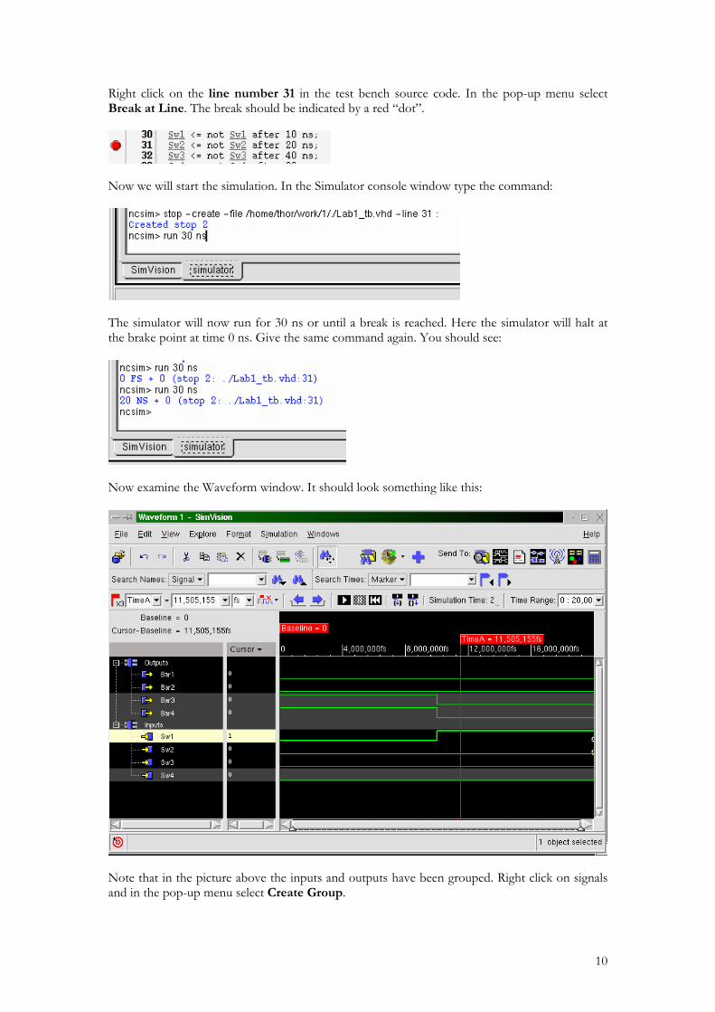
Next select the Lab1.edf file in the Sources window. Next right click Implement Design in the Processes window and select Options. In the window that appears select the Place and Route Properties Tab. Change the default Place and Route Effort Level to High. Click OK.
18
Now right click Implement Design and select Run. The implementation process will now start. After the process is done click the “+” next to Implement Design to expand that view. You should see something like this:

19
Next expand the Generate Post-Place & Route Static Timing. Right click Text-based Place & Route Static Timing Report and select Open Without Updating.
Again the timing information is not very interesting for this lab. However, what you can see is that the pad to pad delays are about 9-10 ns. In order to get a better understanding how logic is implemented in a Xilinx FPGA we will take a closer look at the implemented design. Right click View/Edit Routed Design (FPGA Editor)

20
and select Run.
The FPGA Editor will appear.
The FPGA Editor shows a view of the implemented design. Note that your view might differ as there are several ways to implement the same functionality. The FPGA is an array of Configurable Logic Blocks (CLB) with surrounding programmable interconnections. Input/Output Blocks are located on the edges of the chip. We will take a closer look how the following this line in our VHDL code is implemented: B1 : Bar1 <= (Sw1 and Sw2) or (Sw3 and Sw4); In the List window select All Nets and on the net Bar1_c in the list. The net should be high lighted as shown below.
The tiny design

21
Next click the icon . This will zoom in on the highlighted net. Next zoom in on the “Slice” that drives the highlighted net. A CLB consists of two “slices”
Zoom in here!

22
Now select the slice by clicking on it – it should turn red. Now double click on the slice or click the editblock button on the right edge of the FPGA Editor window. This will open a new
window showing the contents of the slice. In that window click the icon
Here we can see that the AND-OR function is implemented in one Look-Up Table. Now we can close the FPGA Editor and return to the Project Manager window. The last step in the implementation process is to generate the programming file for the FPGA. Right click Generate Programming File and select Run.
Select and double click.
LUT
Function implemented in the LUT

23
Done! Now you are ready to test your design on the XSB boards. 6 Testing the design There are two XSB300E boards available in the hardware lab and they should both be setup and ready for use. Make sure that the ATX power supply is on and check the parallel port connection. Please be careful when you handle the boards. The boards are placed on an ESD protected surface but you don’t have to wear any arm wrist. Just avoid touching the components on the board. Start the tool GXSLoad with the shortcuts in the Windows start menu in XSTools. Locate the lab1.bit file in your lab1/rev1 directory with explorer. Drag and drop the file in the GXSLoad window. Select correct board type. Click Load. When the download is completed press the push buttons on the board and verify the function. Note that when you press a button a ‘0’ will be input to the FPGA.
Over and out.