Embed Size (px)
Citation preview

An Enhanced 32-Bit Processor Core for FPGA Integration

2
Contents
• MicroBlaze 4.0 and FPU• Area and Performance Statistics• Comparison with other processors implemented
on FPGA fabric• Conclusions

3
Some Virtex FPGA basics
• LUT• LUT + FF• Slice, CLB• Interconnect• BRAMs 18Kbit dual ported memory• PPC 405 processors• High speed serial I/O
4
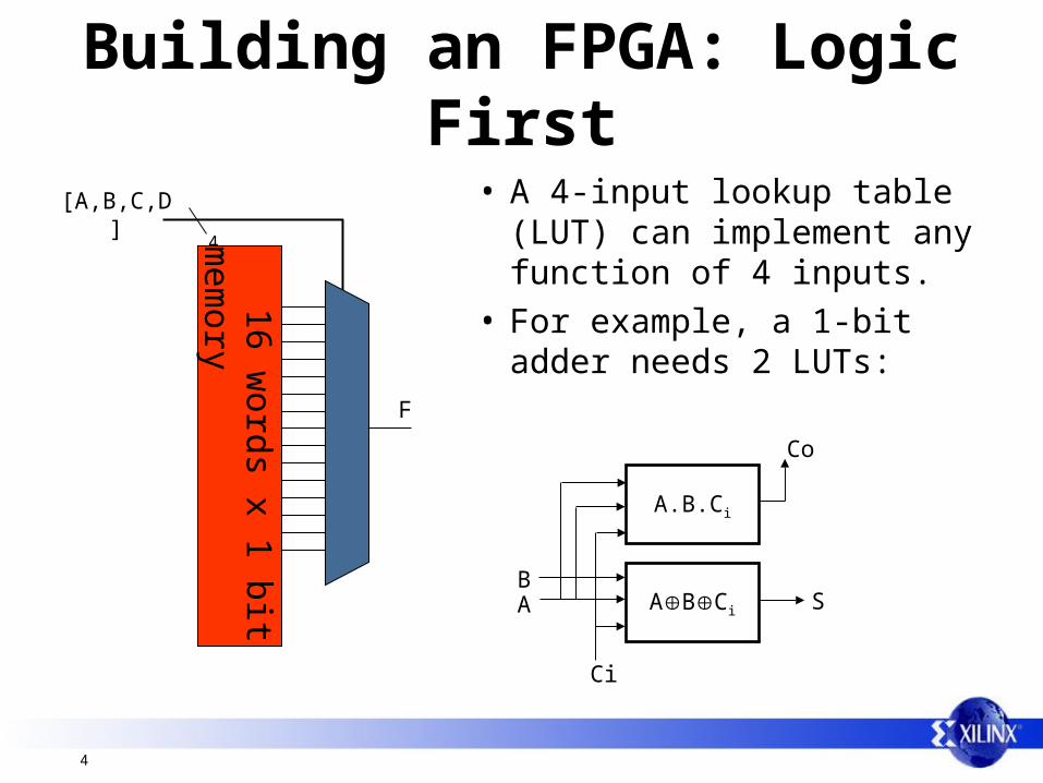
4 16 words x 1 bit m
emory
[A,B,C,D]
F
• A 4-input lookup table(LUT) can implement any function of 4 inputs.
• For example, a 1-bit adder needs 2 LUTs:
ABCi
A.B.Ci
AB
Ci
Co
S
Building an FPGA: Logic First

5
Out
In4
FF
CE RST
M
16 words x 1 bit m
emory
M
M
ClkCERst
Add FF to make a Logic Cell

6
4
FF
CE RST
M
16 words x 1 bit m
emory
Carry M
M
M
DinWECin
Cout
• Make LUT RAM a user resource.
• Fast carry ripple to neighbor.
Arithmetic, Distributed RAM

7
4
4
4
4
4
4
4
4
40
• Group logic cells to reduce overhead.
• Add H, V routing channels with switchboxes.
• Add input, output MUXing between logic and routing.
Add Interconnect

8
4
4
4
4
4
4
4
4
40
4
4
4
4
4
4
4
4
40
4
4
4
4
4
4
4
4
40
4
4
4
4
4
4
4
4
40
Build an Array
9
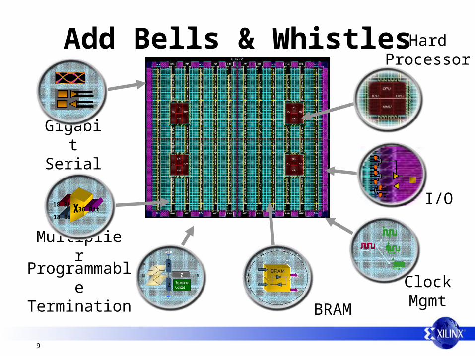
Add Bells & Whistles HardProcessor
I/O
BRAM
Gigabit Serial
Multiplier
ProgrammableTermination
Z
VCCIO
Z
Z
ImpedanceControl Clock
Mgmt
18 Bit
18 Bit36 Bit
CPU Design in FPGA

11
Instruction Set
• Instruction Set must match the building blocks– MicroBlaze has 4 logical instructions
• 4-input LUT can process– 1 bit from two different operands => 2 bits– 2 bits as the operations => 4 different instructions
– 3 logical instructions would create the same size– 5 logical instructions would double the size
12
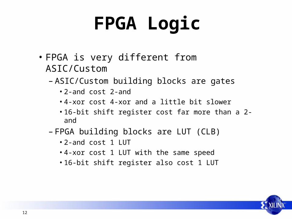
FPGA Logic
• FPGA is very different from ASIC/Custom– ASIC/Custom building blocks are gates
• 2-and cost 2-and• 4-xor cost 4-xor and a little bit slower• 16-bit shift register cost far more than a 2-and
– FPGA building blocks are LUT (CLB)• 2-and cost 1 LUT• 4-xor cost 1 LUT with the same speed• 16-bit shift register also cost 1 LUT

13
Datapath
• A multiplexer cost as much as a ALU (1 LUT/bit)• Deep pipeline creates many muxes due to forwarding• Too deep pipeline will runs slower than a shallow• 3-4 pipeline stages with full forwarding is optimal• >4 pipeline stages will run slower and be bigger

14
Implementation
• Need to use the fastest logic in FPGA– Carry-chain has a delay of 10 ps– MicroBlaze is trying to put anything timing
critical on the carry-chain– ex. Jump Detection Logic– Maximize the usage of LUTRAM, SRL16 and
all features of the flipflops

15
Implementation Characteristics
• FPGAs are really good at networks of ALUs, e.g. put the whole compute graph in there.
• FPGAs are really good at embedded memory if it fits
• Multiplexers are relatively expensive• Different scaling for ALUs and Registerfiles• Larger processors are not cheap in FPGAs, e.g.
PCC 405, a Philips Trimedia 5-issue VLIW.

16
Jump detection logic (standard)
INIT=0001
INIT=0001
Reg_Is_Zero
Vcc
LUT4
LUT4
Reg(28)Reg(29)Reg(30)Reg(31)
Reg(0)Reg(1)Reg(2)Reg(3)
MUXCY
MUXCY
LUTLUT
LUTJump
~= 2 ns
0 1
0 1
17
Jump detection logic (optimal)
Reg_Is_Zero
INIT=0001
INIT=0001
Vcc
LUT4
LUT4
Reg(28)Reg(29)Reg(30)Reg(31)
Reg(0)Reg(1)Reg(2)Reg(3)
MUXCY
MUXCY
LUT
Jump
~= 0.02 ns0 1
MultAnd
0 1
LUT 0 1
MultAnd
0 1

18
Muxing with flipflops
Set
ResetIN OUT
CE
LUT4Set
ResetIN OUT
CE
Set
ResetIN OUT
CE
Set
ResetIN OUT
CE
Clock
Sel1In1
Sel2In2
Sel3In3
Sel4In4

19
Maintenance
• A soft processor is very configurable– How to optimize the implementation without too
many variants? – Avoid to much low-level and only do it when
necessary– MicroBlaze is a mixture of very detailed
implementation and pure RTL code

20
MicroBlaze v4.00 Block Diagram
IOPB – Instruction side On-chip Peripheral BusDOPB – Data side On-chip Peripheral BusILMB – Instruction side Local Memory BusDLMB – Data side Local Memory BusBus IF – Bus Interface
IXCL_M – Instruction side Xilinx Cache Link MasterIXCL_S – Instruction side Xilinx Cache Link SlaveDXCL_M – Data side Xilinx Cache Link MasterDXCL_S – Data side Xilinx Cache Link SlaveMFSL – Master Fast Simplex LinkSFSL – Slave Fast Simplex Link
FPU
Multiplier
Increased Clock Frequency
EnhancedDebug
Enhanced CPI
User Configurable Options

21
MicroBlaze v4.00 FPU
• Single-precision floating-point option – IEEE-754 compatible
• Tightly coupled with CPU– Up to 120x speedup over software FP emulation
• User-configurable option for MicroBlaze core in award-winning Xilinx Platform Studio tool suite
• Zero cost when not used– 1,000 LUTs otherwise

22
Tightly Integrated FPU• Matched maximum clock frequency
– FPU, MicroBlaze pipeline run at the same frequency• Low latency
– FP operands use native CPU registers – FP instructions directly integrated in data flow
• Optimum resource utilization– Reuse already existing pipeline resources– FPU adds just 1,000 LUTs to MicroBlaze
=> Best of both worlds:– Optimized for cost and performance
23
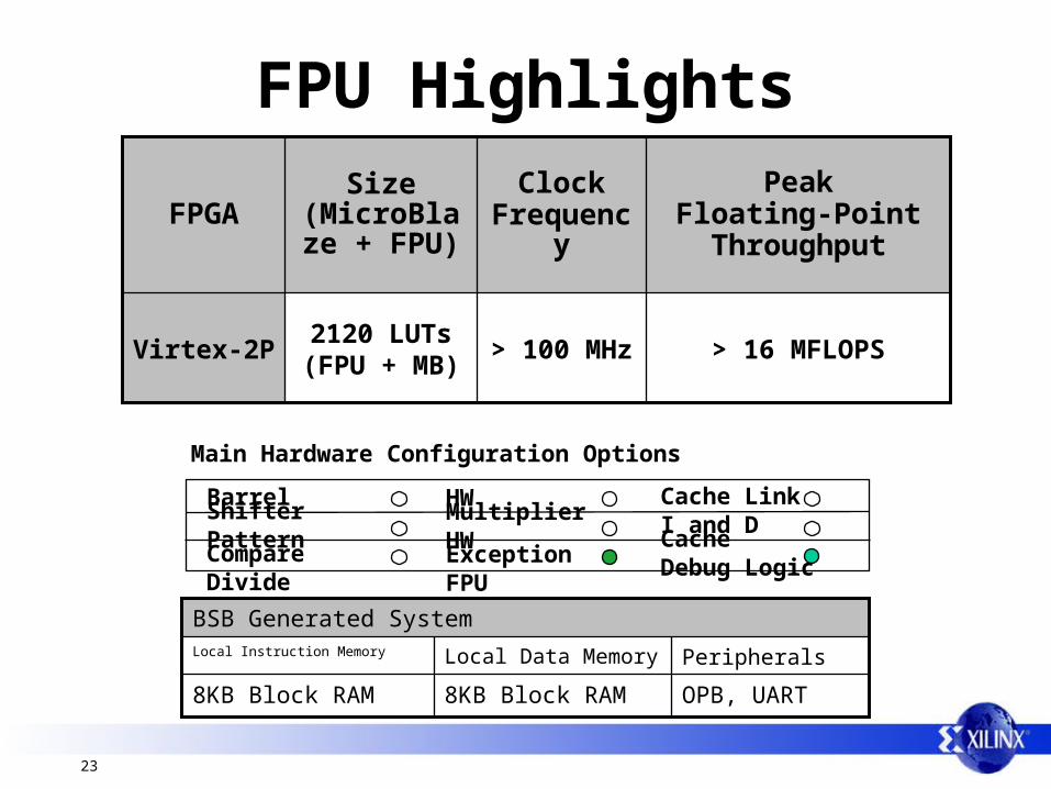
> 16 MFLOPS
PeakFloating-Point
Throughput
> 100 MHz
ClockFrequency
Size (MicroBlaze
+ FPU)FPGA
2120 LUTs(FPU + MB)
Virtex-2P
FPU Highlights
Main Hardware Configuration Options
Barrel ShifterPattern CompareDivide
HW MultiplierHW ExceptionFPU
Cache LinkI and D CacheDebug Logic
BSB Generated System
8KB Block RAM
Local Data Memory
OPB, UART8KB Block RAM
PeripheralsLocal Instruction Memory

24
HW FPU Instructions vs. SW Emulation
gesf2
nesf2
gtsf2
lesf2
eqsf2
ltsf2
divsf3
mulsf3
subsf3
Addsf3
SoftwareFunction
350
350
350
350
350
350
600
1200
450
450
Instructions
450
450
450
450
450
450
750
1600
600
600
Cycles
Less-or-equal floating-point comparison3fcmp.le
Less-than floating-point comparison3fcmp.lt
Equal floating-point comparison3fcmp.eq
Greater-than floating-point comparison3fcmp.gt
Not-equal floating-point comparison3fcmp.ne
Greater-or-equal FP comparison3fcmp.ge
Floating-point arithmetic division30fdiv
Floating-point arithmetic multiplication6fmul
6
6
Cycles
Reserve FP arithmetic subtractionfrsub
Floating-point arithmetic addfadd
DescriptionMicroBlaze FPU Instruction
Cycle time reduced usingMicroBlaze FPU

25
FPU Performance vs. Software
0
20
40
60
80
100
120
JPEG FFT FIR
Factor of speedup
over software FP
6X
50X
120X

26
Complete FP Support• Loads/stores use standard MicroBlaze instructions • Infinity, signed zeros follow IEEE-754 conventions• Software libraries for additional FPU operations
– Rounding– Square root– Conversions– Other floating-point library functions
=> FPU operations seamlessly supported by standard programming model

27
MicroBlaze v4.00 Debug Logic
• New debug logic– Inserts instructions into the pipeline– Access to anything that instructions can access– Packetized data-transfer protocol
• Immediate value to users:– Less debug logic — reduced by 50%– Faster download — up to 15x faster– Access to all registers, including ESR, EAR, and FSR

28
RegFileread
MX2MX3
Rb
RaI-Cache>
I-LMB>
PreFetchBuffer
>
>
FF1
PC_OF>
MX1
+4
MX5
MSREARESRFSR
MX4
int_vec
brk_vec
expt_vec
Imm
>
>
>
>
>
>>
>
>
ALU
Shift
FSL get
FSL put
>
>
Barrel Shift
FPU
>MUL
DIV
Jumplogic
RdData
MX11
>
FF7
SteerD-Cache>
WrData
D-LMB>
Addr
>
FF5
>
XCLcntrl
BRAMcntrl
Mirror
OPB
Up to 16 FSL channels
MX12
RegFilewrite
>
IF OF EX
Rd
MicroBlaze v4.00 Pipeline

29
Performance Improvements: Bringing It All Together
• Now supporting GCC 3.4.1 unit-at-a-time compile– Moved up from GCC 2.9 function-at-a-time compile
• New hardware and compiler boost performance– 0.79 DMIPS/MHz to 0.92 DMIPS/MHz
=> Overall performance benefits to users: – 16% performance improvement on integer code– Up to 40% faster string searches– Up to 120x performance improvement on FP code
30
92 DMIPS
138 DMIPS
166 DMIPS
Dhrystone 2.1
100 MHz
150 MHz
180 MHz
Clock
FrequencyPerformanceSizeFPGA
0.92 DMIPS/MHz
1,318 LUTsSpartan-3 (3S1500-5)
0.92 DMIPS/MHz
1,225 LUTsVirtex-II Pro(2VP20-7)
0.92 DMIPS/MHz
1,269 LUTsVirtex-4
(4VLX25-12)
Configured for Performance
Main Hardware Configuration Options
Barrel ShifterPattern CompareDivide
HW MultiplierHW ExceptionFPU
Cache LinkI and D CacheDebug Logic
Performance Optimized Subsystem
16KB Block RAM
Local Data Memory
GPIO, Timer8KB Block RAM
PeripheralsLocal Instruction Memory

31
105 MHz
170 MHz
205 MHz
Clock
FrequencySizeFPGA
983 LUTsSpartan-3
(3S1500-5)
827 LUTsVirtex-II Pro(2VP20-7)
988 LUTsVirtex-4
(4VLX40-12)
Configured for Frequency
Main Hardware Configuration Options
Barrel ShifterPattern CompareDivide
HW MultiplierHW ExceptionFPU
Cache LinkI and D CacheDebug Logic
Frequency Optimized Subsystem
8KB Block RAM
Local Data Memory
GPIO8KB Block RAM
PeripheralsLocal Instruction Memory

32
> 16 MFLOPS
PeakFloating-Point
Throughput
> 100 MHz
ClockFrequency
Size (MicroBlaze
+ FPU)FPGA
~4000 LUTs(FPU + MB)
Virtex-2P
ucLinux System
Main Hardware Configuration Options
Barrel ShifterPattern CompareDivide
HW MultiplierHW ExceptionFPU
Cache LinkI and D CacheDebug Logic
System Configuration
8KB Block RAM
D CacheOPB, UART, MCH Memcon (~1300), EthernetLite (~500)8KB RAM
PeripheralsI Cache

33
Tensilica core example
http://www.xilinx.com/products/logicore/alliance/tensilica/tensilica_xtensa.pdf

34
Soft Processor Comparison
0
10000
20000
30000
40000
# LU
Ts
0
20
40
60
80
100
120
Freq
(MH
z)
LUTs 2120 33840 12332 29622
Freq (MHz) 100 25 33 29
MB+FPU*
Soft PPC*
Tensilica
Tensilica* (L)
• MicroBlaze 4.0 with FPU implemented on V2P FPGA– V2P adds hard PowerPC 405 block to Virtex2 FPGA fabric
• Soft version of PowerPC 405 implemented on Virtex2 FPGA fabric for emulation– No FPU
• Tensilica Xtensa V core implemented on Virtex2 FPGA fabric by Tensilica (small and large variants)– No FPU
• Each V2P70 FPGA on BEE2 Board contains 74448 LUTs

35
RAMP Interests
• Type B Code– Parameterized HDL code (address space, datapath, opcodes, etc)– Xilinx highly interested in outside contributors
• 64 bit address space– 16, 32, 64, 128 … - HDL code scales– GCC support of 64 bit address also available
• DP FP– Xilinx has the operators (DSP library) – SP, DP, in between– Need to integrate into MB
• Cache Coherency– Memory controllers are key– MMU / coherency manager larger than CPU itself
36
Xilinx Interests• Programming models
– #1 obstacle for wider adoption of FPGAs– Cache coherency, partitioning, MP– RTOS, transactions, MPI, etc– Niagara, Cell, etc– Building large(r) chips is easy, Filling them is more challenging
• Help with (soft) architecture development– Memory and communication models – tough– Processor design / architecture – easy, well studied, well published
• Contributing and receiving back– We make money selling chips (FPGAs)– MB made possible by (single) processor work of past 20+ years– MB designed with Type B model in mind– Licensing model to support this
• Need help with programming and architecture of MP systems– Have ideas– Are willing to help
37
Xilinx University Program (XUP)
• Xilinx interface to both University Teaching and Research
• Academic donation program– All Xilinx Development Tools and IP cores available
for donation– Hardware donations of boards and/or silicon– Large Bee2/RAMP participant
• Technical XUP Contact: [email protected]• http://www.xilinx.com/univ/
38
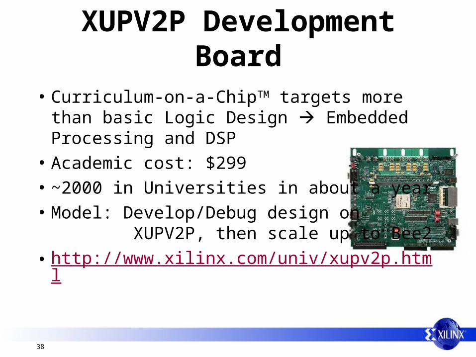
XUPV2P Development Board
• Curriculum-on-a-ChipTM targets more than basic Logic Design Embedded Processing and DSP
• Academic cost: $299• ~2000 in Universities in about a year• Model: Develop/Debug design on
XUPV2P, then scale up to Bee2• http://www.xilinx.com/univ/xupv2p.html