Embed Size (px)
Citation preview

A ADC based Time to Digital Converter
Karthik, Columbia University
EE6901, Spring 2010

Outline
• Motivation for the proposed TDC
• Operation of the proposed TDC
• ADC Requirements
• PFD/CP Design
• Resolution of TDC
• Recommendations for Future work

Motivation
• All digital PLLs: Loop filter using digital filters– Area efficient
– Highly programmable
• TDCs are used to convert phase difference into digital code [1]– Uses time amplification. Similar to two stage ADC.
• Why not use an ADC directly??
• To come up with a TDC based on ADCs that beats the performance of the one in [1]

Block DiagramPFD/CP dumps charge on the cap. Phase is converted to voltage
ADC samples the voltage and converts it into bits
Cap. Voltage is reset to Vcmbefore the next cycle.

Operation
• Reset signal is used to turn ON the ADC enable.
• ADC enable is ON till the voltage to digital conversion is complete
• Cap. Reset signal turns ON after ADC conversion is complete
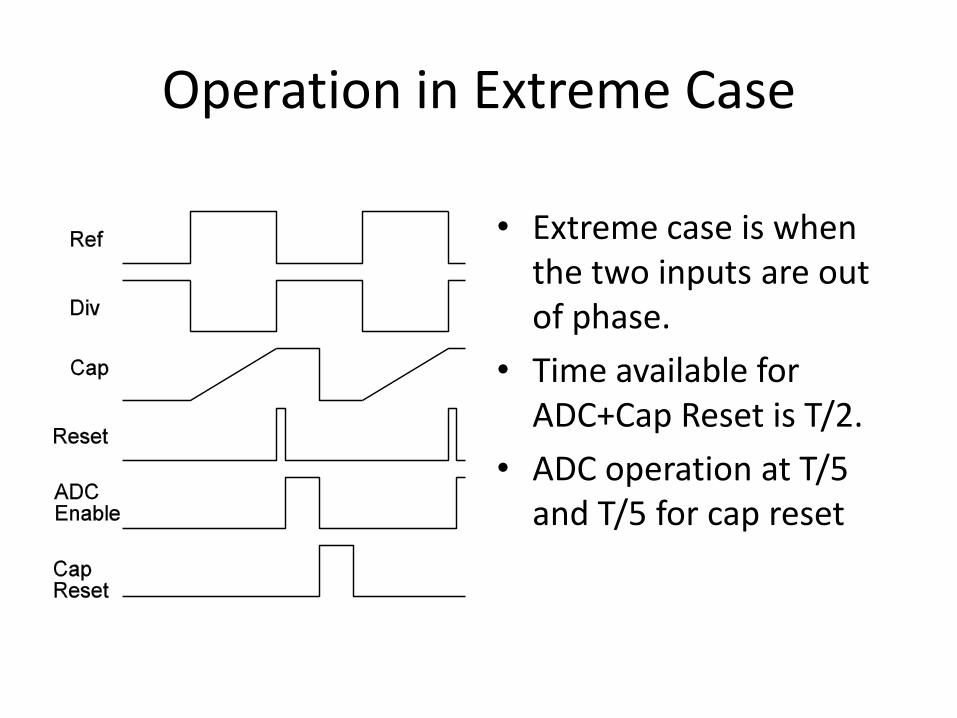
Operation in Extreme Case
• Extreme case is when the two inputs are out of phase.
• Time available for ADC+Cap Reset is T/2.
• ADC operation at T/5 and T/5 for cap reset

Constraints for the TDC
• Power Consumption: < 3mW.
• Resolution : 9bits.
• Frequency of Operation : 10MHz.
• Should improve with technology scaling.
• Latency should be as small as possible.

Choice of ADC
• Pipeline– A 10 bit ADC requires 10 stages.
– 10 clock cycles within T/5 => Pipeline @ 500Msps
– 100mW power
• Delta Sigma– Needs decimation filtering => latency
• SAR– Extremely good FOMs for these speeds and
resolutions. [2], [3]
– Power : 195uW [2], 826uW[3]
– Improves with technology scaling
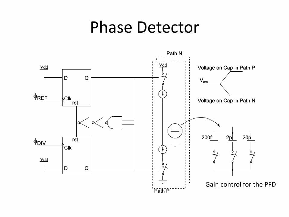
Phase Detector
Gain control for the PFD

Resolution of the TDC
• ADC Resolution: 10bits
– Full scale: 2.4V
– LSB: 2.4mV
• Time resolution is a f(Icp/C). Icp=100uA.
– 2.4ps when C=200fF
– 24ps when C=2pF
– 240ps when C=20pF
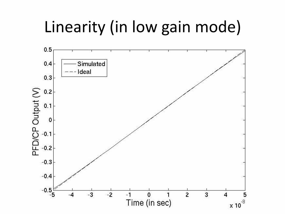
Linearity (in low gain mode)

INL
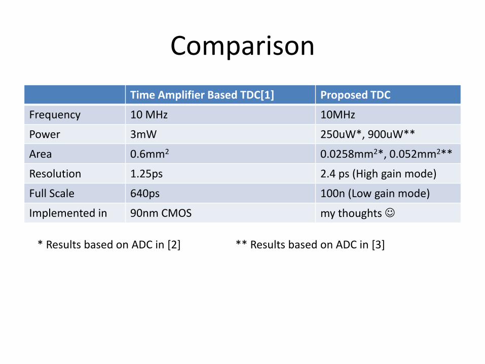
Comparison
Time Amplifier Based TDC[1] Proposed TDC
Frequency 10 MHz 10MHz
Power 3mW 250uW*, 900uW**
Area 0.6mm2 0.0258mm2*, 0.052mm2**
Resolution 1.25ps 2.4 ps (High gain mode)
Full Scale 640ps 100n (Low gain mode)
Implemented in 90nm CMOS my thoughts
* Results based on ADC in [2] ** Results based on ADC in [3]

Conclusions
• When compared to the TDC in [1], the proposed idea would have a
– bigger full scale time range.
– Approximately the same resolution.
– 3X lower power.
– 10X lower area.

Recommendations for Future Work
• PLL Simulation using this TDC.
• Simplification of ADC resolution requirement.
• SAR produces MSBs first. If loop filter could be designed to operate with MSBs, then the speed of the SAR can be reduced without affecting latency.
References
[1] Minjae Lee; Abidi, A.A.; , "A 9 b, 1.25 ps Resolution Coarse–Fine Time-to-Digital Converter in 90 nm CMOS that Amplifies a Time Residue," Solid-State Circuits, IEEE Journal of , vol.43, no.4, pp.769-777, April 2008
[2] van Elzakker, M.; van Tuijl, E.; Geraedts, P.; Schinkel, D.; Klumperink, E. A. M.; Nauta, B.; , "A 10-bit Charge-Redistribution ADC Consuming 1.9 $mu$W at 1 MS/s," Solid-State Circuits, IEEE Journal of , vol.45, no.5, pp.1007-1015, May 2010
[3] Chun-Cheng Liu; Soon-Jyh Chang; Guan-Ying Huang; Ying-Zu Lin; , "A 10-bit 50-MS/s SAR ADC With a Monotonic Capacitor Switching Procedure," Solid-State Circuits, IEEE Journal of , vol.45, no.4, pp.731-740, April 2010