Embed Size (px)
Citation preview

ABSTRACT
Title of Document: SYSTEM ANALYSIS AND DESIGN FOR
THE RESONANT INDUCTIVE NEAR-FIELD
GENERATION SYSTEM (RINGS)
Dustin James Alinger, Master of Science, 2013
Directed By: Professor Raymond J. Sedwick
Department of Aerospace Engineering
The Resonant Inductive Near-field Generation System (RINGS) is a technology
demonstrator experiment which will allow for the first ever testing of electromagnetic
formation flight (EMFF) algorithms in a full six degree of freedom environment on
board the International Space Station (ISS). RINGS is a hybrid design, which, in
addition to providing EMFF capabilities, also allows for wireless power transfer
(WPT) via resonant inductive coupling. This thesis presents an overview of the
mechanical and electrical design of the RINGS experiment, as well as simulation
techniques used to model various system parameters in both EMFF and WPT
operational modes. Also presented is an analytical and experimental investigation of
the influence of the proximity effect on a multi-layer flat spiral coil made from ribbon
wire.

SYSTEM ANALYSIS AND DESIGN FOR THE RESONANT INDUCTIVE NEAR-
FIELD GENERATION SYSTEM (RINGS)
By
Dustin James Alinger
Thesis submitted to the Faculty of the Graduate School of the
University of Maryland, College Park, in partial fulfillment
of the requirements for the degree of
Master of Science
2013
Advisory Committee:
Professor Raymond J. Sedwick, Chair
Professor David Akin
Professor Derek Paley

© Copyright by
Dustin Alinger
2013

ii
Acknowledgements
First, a huge thanks to my advisor, Dr. Ray Sedwick, for conceiving such an
awesome experiment, for giving me the opportunity to work on such a great project,
and for granting me the trust and independence to let me do things my way. His help
and insight over the past few years have been invaluable, and there’s no chance I
would be where I am today had it not been for him.
I also owe a big thanks to Allison Porter, my grad student partner at UMD and
the RINGS software mastermind, for her relentless dedication and contribution to
every facet of the project. I doubt there’s another pair of people on the planet who
could make a coil stack as well as us - may we never have to wrap another layer
again!
Thank you to everybody at Aurora Flight Sciences for their tireless efforts in
getting the flight and engineering units built, and for always making me feel welcome
at AFS. Thanks to John Merk and Charlie De Vivero for their contributions to the
circuit designs, their excellent work in designing all of the RINGS PCBs, and their
help and guidance with all of the electronics design. Thanks to soldering virtuoso
Joanne Vining for the countless hours she put in to populate and coat the boards, and
for teaching me a thing or two with the iron. And finally, thanks to Roedolph
Opperman for his great work designing the RINGS to SPHERES support structure
(which is definitely the best looking part of RINGS), for contributing his valuable
creative insight to any mechanical design problem that came up, and for always
lending a hand with anything RINGS needed.

iii
Thanks are also owed to all those at the MIT SSL who helped make RINGS a
reality. To Alex Buck and Greg Eslinger, thanks for all your exceptional work in
getting RINGS and SPHERES to successfully (and peacefully) interface with one
another, for all the great work testing them on the flat floor, for the huge number of
hours I’m sure you put in to get us ready for the RGA flights, and of course for all the
help in building the engineering and flight units. Thanks to Paul Bauer for all his
help with the drive circuit, for recommending that we use the OSMC, and for
teaching me the importance of reading the data sheet.
Also, thanks to Dr. Peter Fisher at MIT and Elisenda Bou at UPC Barcelona
for all their help with the WPT side of RINGS.
Thanks to all of my labmates at the SPPL and all of my friends for putting up
with the never-ending RINGS talk for the past two years.
Most importantly, thank you to my parents for their continuing love and
support over the years.
Funding for this work was provided primarily by the DARPA InSPIRE
program, through NASA contract number NNH11CC33C. Additional funding was
also provided on the same contract by NASA Headquarters. The author gratefully
acknowledges the support of both agencies.
To everyone on the RINGS team: congratulations, we made one hell of a
payload…
“Is there life on Mars?” – David Bowie

iv
Table of Contents
Acknowledgements ....................................................................................................... ii
Table of Contents ......................................................................................................... iv
List of Tables ............................................................................................................... vi
List of Figures ............................................................................................................. vii
Chapter 1 : Introduction ................................................................................................ 1
1.1 : Electromagnetic Formation Flight .................................................................... 1
1.2 : Resonant Inductive Wireless Power Transfer ................................................... 4
1.3 : Resonant Inductive Near-field Generation System (RINGS) ........................... 5
1.4 : Statement of Contributions ............................................................................... 8
Chapter 2 : Resonant Coil ........................................................................................... 11
2.1 : Design ............................................................................................................. 11
2.2 : Construction .................................................................................................... 19
2.3 : Electrical Testing and Characterization .......................................................... 28
Chapter 3 : Housing and Interior Components ........................................................... 36
3.1 : Housing Design............................................................................................... 36
3.1.1 : Structural Requirements and Design ....................................................... 36
3.1.2 : Cooling Requirements and Thermal Design ............................................ 40
3.1.3 : Electronics Box ........................................................................................ 44
3.2 : Interior Component Design ............................................................................ 47
3.2.1 : Mounting the Resonant Coil .................................................................... 47
3.2.2 : Flow Guide Fins....................................................................................... 49
3.2.3 : Powerbox Fans ......................................................................................... 57

v
Chapter 4 : Electronics ................................................................................................ 61
4.1 : Circuit Design ................................................................................................. 61
4.1.1 : Resonant Coil Drive Circuit .................................................................... 61
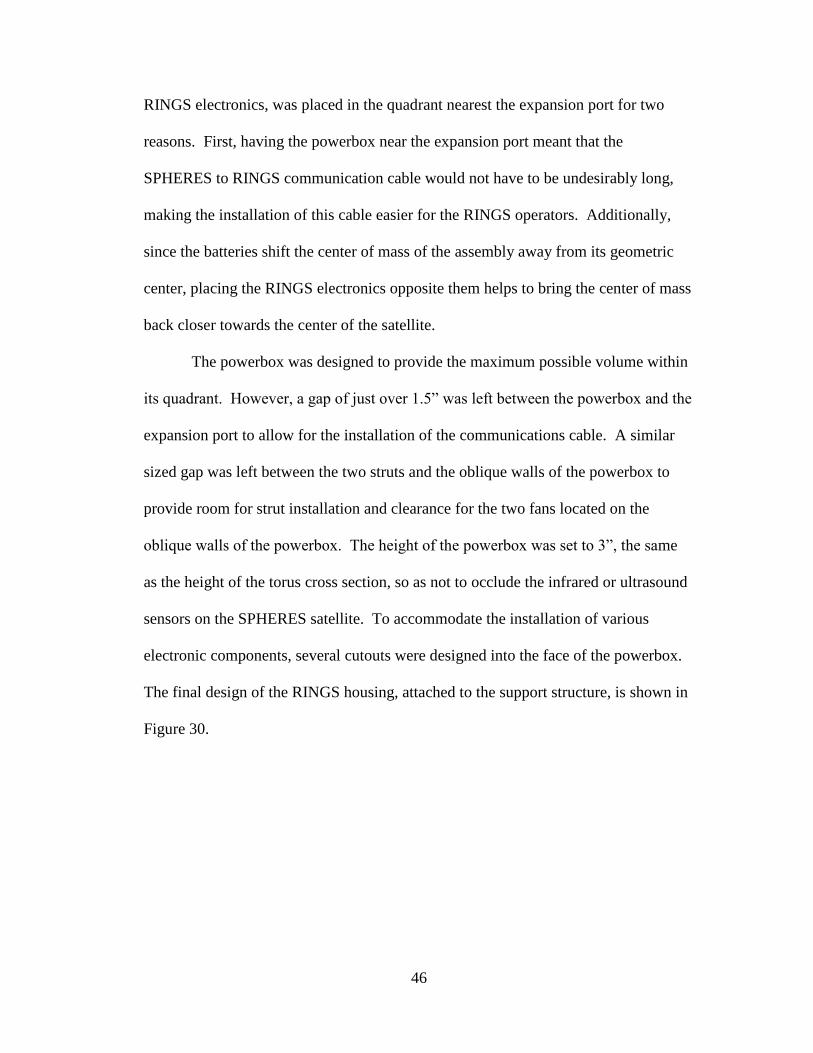
4.1.2 : Low Power Board .................................................................................... 66
4.1.3 : Capacitor Board ....................................................................................... 73
4.1.4 : IR Sensor Board ....................................................................................... 76
4.1.5 : Connector Board ...................................................................................... 78
4.1.6 : Temperature Sensor Board ...................................................................... 79
4.1.7 : Off-Board Components............................................................................ 80
4.2 : Printed Circuit Board Sizing and Mounting ................................................... 82
4.2.1 : LCD Displays, Low Power Board, OSMC and Connector Board........... 83
4.2.2 : Capacitor Board and Relays .................................................................... 85
4.2.3 : IR Sensor Boards ..................................................................................... 89
4.2.4 : Pushbuttons and Switches ........................................................................ 90
Chapter 5 : Simulations ............................................................................................... 93
5.1 : WPT Modeling ............................................................................................... 93
5.1.1 : Resonant Inductive Coupling Model ....................................................... 93
5.1.2 : Load Resistor Sizing ................................................................................ 97
5.2 : Driving Resonant Coil Circuit with Rectangular Wave ............................... 100
5.3 : EMFF Simulations ........................................................................................ 105
5.3.1 : One-Coil Simulations ............................................................................ 105
5.3.2 : Two-Coil Simulations ............................................................................ 110
Chapter 6 : Conclusions ............................................................................................ 114

vi
List of Tables
Table 1 – Major Dimensions of Resonant Coil .......................................................... 16
Table 2 – Drive Circuit Operational Modes ............................................................... 64

vii
List of Figures
Figure 1 – SPHERES Satellites on the ISS ................................................................... 6
Figure 2 – Early RINGS Conceptual Design ................................................................ 7
Figure 3 – Cross-Sectional View of Resonant Coil .................................................... 16
Figure 4 - Double Sided Comb ................................................................................... 17
Figure 5 – Exploded View of Resonant Coil and Combs ........................................... 18
Figure 6 – One of the Eight Comb Locations on the Resonant Coil .......................... 18
Figure 7 – Spool Used to Manufacturer Coil Layers .................................................. 20
Figure 8 – Coil Wire on the Factory Spool ................................................................. 20
Figure 9 – Fully Wrapped Layer with Long Spacers and Short Spacers .................... 21
Figure 10 – Undesirable Winding-to-Winding Contact as a Result of No Heat
Treatment .................................................................................................................... 23
Figure 11 – Short Spacers Removed and Comb Installed into Windings................... 24
Figure 12 – Gluing a Comb in Place with Permabond 820 ........................................ 25
Figure 13 – Coil Layer with Proper Air Gap Between Windings............................... 25
Figure 14 – Electrical Connections on Inner Surface of Coil Stack ........................... 27
Figure 15 – Electrical Connections on Outer Surface of Coil Stack .......................... 27
Figure 16 – Test Setup for Measuring Proximity Effect ............................................. 29
Figure 17 – Frequency Dependent Behavior of Coil Resistance ................................ 31
Figure 18 – Frequency Dependent Behavior of Coil Inductance ............................... 32
Figure 19 – Curve Fit Applied to Measured Resistance Data .................................... 33
Figure 20 – Curve Fit Applied to Measured Inductance Data .................................... 33

viii
Figure 21 – Comparison of Minimum Impedance and Zero Reactance for Resonant
Coil Circuit.................................................................................................................. 35
Figure 22 – Split Torus Housing Concept .................................................................. 36
Figure 23 – Cross-Sectional View of Housing Halves and Resonant Coil ................. 37
Figure 24 – FEA Analysis of Push-off Loading Scenario .......................................... 39
Figure 25 – FEA Analysis of Pick Up Quickly Loading Scenario ............................. 40
Figure 26 – Fan and Diffuser Locations ..................................................................... 42
Figure 27 – Exit Air Diffuser ...................................................................................... 43
Figure 28 – Outer Fan Boss ........................................................................................ 44
Figure 29 – Support Structure and SPHERES Satellite .............................................. 45
Figure 30 – Final Design of RINGS Housing Attached to Support Structure ............ 47
Figure 31 – Comb Support .......................................................................................... 48
Figure 32 – Comb Support Setup................................................................................ 49
Figure 33 – Inner Flow Guide Fin and Inner Fin Mount ............................................ 50
Figure 34 – Inner Fin Setup ........................................................................................ 50
Figure 35 – Outer Fin and Outer Fin Ring .................................................................. 51
Figure 36 – Outer Fin Joint Connections .................................................................... 52
Figure 37 – Outer Fin Setup........................................................................................ 52
Figure 38 – Outer Fan Mounting Setup ...................................................................... 53
Figure 39 – Cross-Sectional View of Outer Fan Mounting Setup .............................. 54
Figure 40 – Comb Support Cross-Sectional View ...................................................... 55
Figure 41 – Resonant Coil Cooling Channel .............................................................. 56
Figure 42 – Outer and Inner Fin Notch Locations ...................................................... 57

ix
Figure 43 – Fan Box ................................................................................................... 57
Figure 44 – Fan Box Assembly .................................................................................. 58
Figure 45 – Fan Box Mounting ................................................................................... 59
Figure 46 – Diffuser Safety Cap ................................................................................. 59
Figure 47 – Diffuser Safety Cap Setup ....................................................................... 60
Figure 48 – Open Source Motor Controller (OSMC) made by Robot Power ............ 62
Figure 49 – RINGS Drive Circuit Schematic ............................................................. 63
Figure 50 – Op Amp for Shifting DC Offset of Hall Effect Sensor Output ............... 70
Figure 51 – Op Amp for Improving Performance of RMS-to-DC Converter ............ 70
Figure 52 – Overcurrent Voting Scheme .................................................................... 73
Figure 53 – RINGS IR Sensor Board Schematic ........................................................ 78
Figure 54 – Resonant Coil Temperature Sensor Board .............................................. 80
Figure 55 – Exit Air Temperature Sensor Board ........................................................ 80
Figure 56 – LCD Mounting Setup with Base Plate and Lens ..................................... 83
Figure 57 – Low Power Board and OSMC Stack ....................................................... 84
Figure 58 – Connector Board ...................................................................................... 85
Figure 59 – Relay Mount and Relay Assembly .......................................................... 85
Figure 60 – Capacitor and Relay Mount Setup ........................................................... 86
Figure 61 – Capacitor Board Setup ............................................................................. 87
Figure 62 – Wire Connections from Capacitor Board to Relays and WPT Capacitor 88
Figure 63 – Overhead View of Capacitor Board with Relays and WPT Capacitor
Installed ....................................................................................................................... 88
Figure 64 – IR Sensor Board Strut Mounting ............................................................. 89

x
Figure 65 – Inner Fin IR Sensor Board ....................................................................... 90
Figure 66 – Rocker Switch and Switch Guard............................................................ 91
Figure 67 – LCD Pushbutton and Low Battery Indicator LED Locations ................. 91
Figure 68 – Master Clear Pushbutton ......................................................................... 92
Figure 69 – Block Diagram for WPT ......................................................................... 93
Figure 70 – Coupling Coefficient vs. Separation Distance......................................... 97
Figure 71 – Power Transfer Levels for Various Load Resistances ............................ 99
Figure 72 – Power Transfer Efficiency for Various Load Resistances .................... 100
Figure 73 – Impedance vs. Duty Cycle for EMFF Mode ......................................... 103
Figure 74 – Impedance vs. Duty Cycle for WPT Transmit Mode ............................ 105
Figure 75 – One Coil EMFF Transient Simulation .................................................. 107
Figure 76 – One Coil EMFF Phase Change Response ............................................. 108
Figure 77 – Coil Currents vs. Duty Cycle in EMFF Mode ....................................... 109
Figure 78 – Block Diagram for Two Coil EMFF ..................................................... 111
Figure 79 – Two Coil EMFF Simulation Results ..................................................... 113
Figure 80 – RINGS Flight Units on the Flat Floor Facility at the MIT SSL ............ 116

1
Chapter 1: Introduction
1.1: Electromagnetic Formation Flight
In the realm of satellite formation flying, a cluster formation refers to a group
of satellites that share nearly identical orbital parameters and are separated by short
distances, typically on the order of hundreds of meters. Sometimes called a cluster
constellation, this arrangement can prove beneficial for several different technologies.
Multiple-aperture interferometry (MAI) is one such technology. In MAI, a group of
images, perhaps of the surface of Earth or another planetary body, are obtained from
several telescopes in close proximity to one another. By cross-correlating these
images, the resulting image resolution is comparable to that captured by a single,
much larger aperture. Such a technique is highly advantageous for space-based
imaging, since the cost of launching multiple smaller telescopes could be significantly
smaller than the launch cost of a single larger telescope. An example of a proposed
orbital MAI system is the U.S. Air Force Research Laboratory’s TechSat-21 program,
cancelled in 2003.
Another proposed technology that would utilize a clustered satellite
arrangement is an architecture known as fractionated spacecraft. In this setup, the
various subsystems typically found on a monolithic satellite are separated into
separate modules. Brown and Eremenko propose in [1] that such a fractionated
architecture would provide improved robustness and reduced development and
operational costs versus traditional monolithic satellite designs.

2
Both of these technologies, and likely any technology based around clustered
formation flight, require some means for controlling the individual attitudes and
relative positions of the individual spacecraft. This control capability is most
obviously necessary to maintain the desired orbit in the presence of disturbances such
as differential drag and Earth oblateness, but could also be used to reposition the
relative location of the individual satellites within the formation, perhaps to obtain
some optimal spacing for MAI imaging. The traditional approach to providing such
attitude and position control is through the use of propellant-based propulsion
systems. However, this approach ultimately limits the operational lifetime of the
cluster due to the finite amount of available propellant onboard a spacecraft.
Electromagnetic formation flight (EMFF) is a propellant-less propulsion technology
which aims to mitigate the operational lifetime constraints presented in a thruster
based setup.
In an EMFF approach, each spacecraft in the cluster generates a magnetic
field by circulating current through onboard wire coils. The interaction of these
magnetic fields produces electromagnetic forces and torques that can be used to
maneuver the individual satellites within the cluster. Due to conservation of
momentum, the location of the center of mass of the cluster cannot change, but the
spacecraft can be reoriented relative to one another. The energy required to drive
current through the coils can be supplied by solar panels, eliminating the problem of
limited consumables.
A full-fledged EMFF setup would include three orthogonally aligned coils on
each spacecraft, to allow for the creation of a steerable magnetic dipole in all three

3
dimensions. Due to angular momentum conservation, an electromagnetic torque is
produced in addition to the electromagnetic force, and as a result EMFF alone cannot
provide attitude control. Instead, attitude control must be supplied through other
means such as reaction wheels or control momentum gyroscopes.
In 2005, a two-dimensional ground-based EMFF testbed was created at the
Massachusetts Institute of Technology (MIT) Space Systems Laboratory (SSL) [2]. It
featured two vehicles, designed to operate on a flat floor using air carriages. Each
vehicle contained two orthogonally aligned coils made from high-temperature
superconducting (HTS) wire, as well as one reaction wheel. Due to the high currents
needed to generate appreciable forces and torques over typical formation flight
distances, HTS wire is an enabling technology for longer range EMFF. The power
dissipation in traditional conductors at these high currents is prohibitively large, but
this problem is eliminated in an HTS coil design. However, an HTS system is
inherently more complex due to the thermal control system required to keep the wire
at its superconducting temperature.
A non-superconducting EMFF testbed was also developed at the MIT SSL
which used coils made from aluminum wire [3]. This one-dimensional proof-of-
concept system, called micro-EMFF (µEMFF), was used to verify simulation models
and to investigate various EMFF control algorithms. Most importantly, the µEMFF
testbed successfully demonstrated that close proximity EMFF operations are feasible
using coils made from conventional conductors.

4
1.2: Resonant Inductive Wireless Power Transfer
Wireless power transfer (WPT) using resonant inductive coupling is a means
of non-radiative energy transfer. This technology exploits the fact that two resonators
that are tuned to the same natural frequency will couple strongly to one another, but
weakly into other objects that do not have the same resonant frequency, minimizing
losses into the environment. In a magnetic induction setup, the resonators are made
from coils of wire through which alternating current (AC) is driven. Circulating AC
current through a source coil (also called a primary coil) generates an oscillating
magnetic field which induces an electromotive force (EMF) in a receiver coil (also
called a secondary coil). This EMF causes current to flow in the secondary coil,
allowing for the wireless transfer of energy. A common example of a device that
transfers power via inductive coupling is an electric toothbrush charger; however, the
performance of such a system degrades rapidly as the distance between the source
and receiver is increased, due to the small size of the coils used and the fact that the
two coils are not operated at resonance. In a resonant system, the inductive reactance
of the coils is cancelled by the capacitive reactance (either from the self-capacitance
of the coil in a self-resonant system, or from that of an associated loading capacitor),
which dramatically reduces the coil impedance at the resonant frequency. Since the
power transfer efficiency is proportional to the frequency of operation, a system with
a high resonant frequency is desirable. However, a tradeoff exists due to the fact that
the coil resistance increases with frequency due to the skin effect, radiative losses etc.
Nikola Tesla first demonstrated WPT via resonant inductive coupling in the
early 1900’s [4]. However, very little further research was conducted on the topic for

5
over 100 years, most likely due to the lack of a pressing need for the wireless transfer
of power at high efficiencies over moderate distances. With the advent of portable
electronics, the technology has in the last ten years become one of great interest. In
2007, researchers at MIT demonstrated, via resonantly tuned coils, the wireless
transfer of 60 watts at 40% efficiency over a distance of 2 meters [5]. This system
used helical coils made from copper wire with a self-resonant frequency of
approximately 10 MHz. A paper by the same team of researchers presented a
framework for analyzing the resonant coupling system performance using coupled-
mode theory [6]. Their results highlight the advantage of a resonant inductive
system, as the analysis indicates that the resonant scheme can transfer 106 times more
power than a typical non-resonant setup.
1.3: Resonant Inductive Near-field Generation System (RINGS)
Due to the physical similarities of the coils required for both EMFF and
inductively coupled WPT, a hybrid system is an appealing option. The design of one
such hybrid system, called the Resonant Inductive Near-field Generation System
(RINGS), is the primary focus of this thesis.
RINGS is a technology demonstrator experiment consisting of two vehicles
that will launch to the International Space Station (ISS) in the summer of 2013. Its
goals are to demonstrate the feasibility of, and provide a testbed for, EMFF
operations in a full 6 degree of freedom (DOF) environment. Additionally, RINGS
will demonstrate resonant inductive WPT on the order of tens of watts over distances
of approximately 1 meter.

6
Launched to the ISS in 2006, the Synchronized Position Hold, Engage,
Reorient Experimental Satellites (SPHERES) experiment serves as a testbed for
formation flight. The SPHERES satellites, shown in Figure 1, feature a metrology
system that uses ultrasound and infrared sensors to determine both the position and
attitude of the satellites within their operational volume on the ISS. Additionally,
each SPHERE contains 12 CO2 thrusters that allow them to maneuver within the test
environment. This overall setup allows for the testing of various formation flight
control algorithms in the full 6 DOF micro-gravity environment provided by the ISS.
The SPHERES expansion port allows subsequently launched ISS payloads to
interface with the satellites for various science purposes.
Figure 1 – SPHERES Satellites on the ISS
The RINGS vehicles are designed to attach to the SPHERES satellites and
integrate with them through the expansion port. RINGS will utilize the SPHERES
metrology system, allowing for the testing of various EMFF control algorithms. By
firing their CO2 thrusters in orthogonal pairs, the SPHERES satellites will provide the

7
torque control necessary for EMFF maneuvers. An early conceptual design for
RINGS is shown in Figure 2.
Figure 2 – Early RINGS Conceptual Design
The most important component of the RINGS vehicles is the wire coil, called
the “resonant coil,” which is used to generate the oscillating magnetic field used for
EMFF operations and for WPT. While previous EMFF testbeds circulated direct
current (DC) through the coil, RINGS is designed for AC EMFF operations. The
main reason for this design decision is that a DC system is subject to parasitic torques
caused by the coil’s interaction with the Earth’s magnetic field. An AC architecture,
however, does not experience these parasitic torques. Additionally, since the coil
currents must be AC for inductive WPT to occur, the overall coil drive circuit setup is
simplified if EMFF is also operated at AC.

8
1.4: Statement of Contributions
The design, development, and construction of the RINGS experiment has been
a largely collaborative effort. Significant contributions were made by other
researchers from the University of Maryland Space Power and Propulsion
Laboratory, our colleagues at Aurora Flight Sciences, as well as students and
professors at the Massachusetts Institute of Technology Space Systems Laboratory.
This thesis, however, aims to highlight the work to which the author made a distinct
contribution.
The salient contributions of this work to the state of the art are as follows:
1. Design and construction of the first alternating current implementation of
an EMFF system. Because the torque generated between two magnetic
dipoles is proportional to the product of those dipoles, a direct current
system, such as those presented in [2] and [3], interacts with the Earth’s
magnetic field, producing a net parasitic torque. If one of the dipoles is
oscillating, however, the product of that dipole with the Earth’s static
dipole has an average value of zero, and no torque is generated.
2. Implementation of the first system which is capable of both
electromagnetic formation flight and wireless power transfer, and the
lessons learned regarding tradeoffs in coil design to optimize performance
for both technologies. The ability to transfer power between vehicles
could be a benefit to a satellite cluster that utilizes electromagnetic

9
formation flight technologies, so a hybrid EMFF/WPT design is an
attractive option.
3. Development of practical construction techniques for manufacturing a
multi-layer, low-dielectric flat spiral coil made from uninsulated ribbon
wire. The space between the windings of an inductive coil is typically
occupied by wire insulation. By removing this insulation, cooling air can
penetrate the innermost windings of the coil, enhancing thermal
performance and allowing for higher levels of power dissipation.
Additionally, the low-dielectric loss design could be applied to self-
resonant coils to improve their performance, since an uninsulated coil is
not subject to dielectric losses in the insulation.
4. Experimental investigation of frequency variation of coil impedance up to
8 kHz, showing that the Dowell method [7] is largely inaccurate for such a
compact coil design. Coil resistance and inductance change with
frequency, which is a critical factor in determining the optimum power
coupling frequency for a resonant inductive WPT system. Due to the
large discrepancy between the analytical predictions of the Dowell method
and the experimental results obtained, attempting to optimize a coil design
using the Dowell method alone may prove unsuccessful.

10
5. Development of an analytical model of power coupling losses for a
resonant inductive WPT system and application of this model to optimize
performance for the presented coil design. The model examines the
system in the frequency domain using a traditional block diagram
composed of transfer functions, which is simpler to manage and more
intuitively clear than a system of differential equations. This has value as
a design tool, as it allows for the predicting of performance for different
system parameter values, such as load resistance, operational frequency,
etc.
6. Development of an analytical method for predicting the effective overall
impedance of a coil whose impedance varies with frequency for the case
of non-sinusoidal applied voltage waveforms. The examples presented in
this thesis explore the case of an applied AC rectangular wave, but this
method could be applied to any non-sinusoidal input, such as sawtooth or
triangle waveforms, for any coil whose inductance and resistance are
frequency dependent.

11
Chapter 2: Resonant Coil
2.1: Design
Early in the design process for the resonant coil, the decision was made to
construct the coil from uninsulated wire having a rectangular cross section, also
known as “ribbon” wire. The primary reason for this is the thermal advantage that it
presents over a coil made from insulated wire. Power dissipation due to ohmic losses
in the wire will cause the wire temperature to increase. The micro-EMFF testbed
presented in [3], which utilized insulated wire coils, was ultimately limited by this
power dissipation. To prevent the micro-EMFF coils from overheating required using
pulsed currents of short duration or low amperage. RINGS was designed to operate
continuously over a period of minutes or hours, and had the added constraint of
operating in a microgravity environment where free convection does not exist. To
maintain a healthy operating temperature, cooling fans had to be included to circulate
air over and through the resonant coil. By eliminating the insulation, airflow from the
fans is able to penetrate the inner windings of the coil, resulting in significantly
improved cooling performance. A second reason for using ribbon wire is that its
rectangular geometry is inherently easier to affix parts to than is wire with a round
geometry. This allowed us to construct a coil with a secure, rigid geometry that could
be firmly mounted within the coil housing.
The three basic design parameters for the resonant coil are the electromagnetic
force generated between the two coils, the power dissipated in the coil due to ohmic
losses, and the combined mass of the coil and SPHERES satellite. Using the far-field

12
approximation presented in [3], the force between two axially aligned coils can be
approximated by
(1)
where µ0 is the permeability of free space (4π × 10-7
N∙A-2
), I is the current in the
wire in amps, N is the number of turns of wire, r is the coil radius in meters, and D is
the axial separation distance of the two coils in meters. The power dissipated in the
coil due to ohmic losses is approximated by
(2)
where R is the resistance of the coil in ohms, is the resistivity of the wire material
in µohm∙cm, is the wire width in millimeters, and is the wire height in
millimeters. The combined mass of the SPHERES satellite and the coil is
approximated by
(3)
where MS is the mass of the SPHERES satellite in kilograms and is the mass
density of the wire material in g∙cm-3
. Equations (1), (2) and (3) can then be
combined into a single cost function given by
(4)
Based on operational volume constraints within the ISS, the mean radius of
the coil was chosen to be approximately 30 centimeters. This coil size also
comfortably encircled the SPHERES satellite while still providing ample room for the

13
RINGS to SPHERES support structure and the RINGS electronics. Both copper and
aluminum were considered for the wire material, but we see in (4) that the product of
mass density and resistivity needs to be minimized to increase system performance.
This product is 50% lower for aluminum than it is for copper, despite the lower
resistivity of copper. For this reason, as well as due to its wide commercial
availability, aluminum was selected as the wire material.
The cost function given in (4) is composed of two terms. With the coil radius
and separation distance fixed, the first term is ultimately governed by the material
properties of the wire, namely its resistivity and mass density. The second term is
governed by the coil geometry, represented by the product . It was decided to
weight these two terms equally, which required that ≈ 800 mm2. Prior
experience in the University of Maryland Space Power and Propulsion Laboratory
(SPPL) with manufacturing similar coils from superconducting tapes led to the
selection of a wire aspect ratio, , of roughly 6 to 1. Choosing = 1 mm and =
6 mm resulted in a number of turns, N, of 140, and a total coil mass of 4.25 kg. To
achieve a mostly square overall cross section for the coil, it was decided to split these
140 turns into 7 layers of 20 turns per layer, with each of the 7 layers connected
electrically in series. The prescribed height and width dimensions also provided a
wire cross section with a good size and profile for attaching “combs”, which are
components used to prevent wire windings from contacting one another and are
discussed in more detail later in this section. The distance between adjacent turns
was chosen to be 1 mm, which was a compromise between manufacturability and the
desire for a compact coil cross section. Additionally, the decision for the distance

14
between windings to be equal to the thickness of the wire itself dramatically
simplified the manufacturing process, which is explained further in Section 2.2.
The maximum design current in the coil was calculated from the force
required to execute a baseline circular maneuver. The parameters of this maneuver
are that the RINGS complete a circular rotation about their common center of mass in
a period of 1 minute with an axial separation distance of 1.5 meters. These times and
forces are similar to those of commonly executed SPHERES maneuvers. The
required centripetal force on a vehicle is given by
(5)
where m is the total mass of the RINGS vehicle (including the SPHERES satellite), D
is the axial separation distance, and T is the period of rotation. By setting equations
(1) and (5) equal, we calculate the required number of amp-turns as
(6)
In addition to the coil itself, the final RINGS assembly would also have to contain
other elements such as a support structure for attaching to SPHERES, a housing to
encompass the coil, and other heavy items. As such, the mass of the entire
operational vehicle was estimated to be three times the mass of the coil itself, plus the
additional 4 kg of the SPHERES satellite.
The resulting root mean square (RMS) current required was calculated to be
2100 amp-turns RMS, or 15 amps RMS circulating through the 140 turn coil. The

15
resulting coil resistance was approximately 1.4 Ω and the dissipated power at 15
amps RMS was about 315 watts.
After becoming aware of the significant amount of time and effort required to
manufacture a single layer of the coil, the decision was made to reduce the number of
layers to 5 instead of 7, resulting in a 100 turn coil. As an added benefit, the 100 turn
coil had a squarer cross section than the 140 turn coil, which was more desirable from
a packaging standpoint and also reduced its resistance to approximately 1 Ω. At this
point, the thermal design was already finalized to our original design point of 315
watts of power dissipated in the coil. To utilize the same power dissipation level, the
maximum coil current was increased from 15 to 18 amps RMS. As a result, the total
number of amp-turns at maximum current was decreased slightly from 2100 amp-
turns to 1800 amp-turns. However, due to the 1/D4 force scaling, reducing the
separation distance of the baseline maneuver by 7% (or only by 9 cm) compensated
for the decrease in force while still achieving the rotational period of 1 minute.
The final design of the coil cross section is shown in Figure 3, with the key
dimensions being summarized in Table 1. The notation used for the coil dimensions
in Figure 3 and Table 1 have been modified so as to agree with the notation
commonly used in the Dowell method for evaluating the change in coil impedance
with frequency, the details of which are discussed in Section 2.3. The final alloy
selected for the wire material was 6061 aluminum. This choice was made due to the
desirable heat treatment properties of 6061, as well as the availability of this alloy in
the cross-sectional dimensions (0.040” x 0.250”) that were needed.

16
Figure 3 – Cross-Sectional View of Resonant Coil
Table 1 – Major Dimensions of Resonant Coil
Dimension Description Value
a Breadth of a conductor 6.350 mm
b Winding breadth 36.830 mm
h Height of a conductor 1.016 mm
u Height of an interlayer gap 1.016 mm
Nl Number of turns per layer 5
0.862
lT Mean turn length 200.289 mm
m Number of layers 20
Resistivity 3.700E-8 -m

17
To prevent neighboring windings from contacting one another and to help to
maintain a rigid coil geometry, a polycarbonate part known as a “comb” was
designed, as shown in Figure 4. Each comb has 20 grooves into which the windings
of each layer are glued. Eight of these combs are placed on each layer of the coil
with equal spacing in the circumferential direction. To minimize their impedance to
the cooling airflow, the part was designed to have a very small volume in comparison
with the total inter-winding and inter-layer volume within the coil. There are two
types of combs used: double-sided combs, which have grooves on both sides, and
single-sided combs, which have the same outer dimensions as the double-sided combs
but only have grooves cut into one side. Single-sided combs are placed on the outer
surfaces of the top and bottom layers, and double-sided combs are used between
layers. The double-sided combs also serve to prevent inter-layer wire contact by
providing an air gap of 0.050” between layers. The single-sided combs provide a
means to secure the resonant coil within the housing, as will be discussed later.
Figure 4 - Double Sided Comb

18
A total of 48 combs are installed in the resonant coil – 32 double-sided combs
and 16 single-sided combs. Figure 5 shows an exploded view of the resonant coil and
comb setup, with the coil layers shown in blue and the combs shown in red for clarity.
Figure 6 shows a collapsed view of the same components, with the camera zoomed in
on one of the eight comb locations.
Figure 5 – Exploded View of Resonant Coil and Combs
Figure 6 – One of the Eight Comb Locations on the Resonant Coil
It should be noted that the cross-sectional view shown in Figure 3 is an
approximation, since successive layers of the coil spiral in opposite directions. More

19
specifically, layers 1, 3 and 5 are right-handed spirals and layers 2 and 4 are left-
handed spirals. Since the end of one layer is connected to the beginning of the next
layer, the alternating spiral design allowed for the layer-to-layer electrical
connections to be made in a compact manner. Had all five layers spiraled in the same
direction, the innermost winding of one layer would have to connect to the outermost
winding of the next layer. This would require a jumper wire to be routed either above
or below the entire stack, which was undesirable from a packaging standpoint. The
inter-layer electrical connections are discussed further in Section 2.2.
2.2: Construction
The resonant coil was manufactured one layer at a time using a specially
made, two-piece spool, which is shown in Figure 7. The inner piece of the spool has
a spiral cut of the proper dimensions along its outer circumference, as well as a notch
cutting in towards the center of the part, which provided a location to firmly anchor
the wire at the beginning of the wrapping process. The backing plate of the spool is
larger in diameter than the inner piece and provides support to the wire as it is
wrapped around the inner piece. Both parts of the spool are made from 6061
aluminum and have 8 notches located around their circumference to allow for the
installation of the combs.

20
Figure 7 – Spool Used to Manufacturer Coil Layers
The coil wire arrived wrapped on a factory spool, as shown in Figure 8, which
had a much smaller diameter than was required for the coil layers. At the start of the
wrapping process, a small 90 degree bend was made in the end of the wire and this
bend was inserted into the notch on the two-piece spool. Then, the wire was carefully
unwound from the factory spool and wrapped onto the two-piece spool.
Figure 8 – Coil Wire on the Factory Spool
As the wire was wrapped, “spacers” were regularly inserted around the
circumference of the spiral so as to properly space out the windings of the layer.

21
These spacers were cut from the wire itself, since the desired gap between windings
(0.040”) was the same thickness as the wire. Two types of spacers were used, called
long spacers and short spacers. Long spacers were of an appropriate length to nearly
span the distance between adjacent spool notches. Short spacers were slightly longer
than the width of the notch. A section of one fully wrapped layer is shown in Figure
9. Throughout the wrapping process, the coil wire was periodically pulled on with a
pair of pliers in order to ensure a tightly packed, snug wrap with no visible gaps
between the coil wire and the spacers.
Figure 9 – Fully Wrapped Layer with Long Spacers and Short Spacers
While only 20 windings per layer were required for the design, each layer was
wrapped with at least 23 windings. Later in the construction process, these excess
windings were trimmed away to leave a coil with the desired number of 20 windings.
The reason for wrapping a few additional windings was that after the wire was
released from the pliers, the first one or two of the outermost windings tended to
loosen slightly. For the windings away from the outermost windings, however,
friction between the coil wire and spacers prevented them from loosening. After at

22
least 23 windings had been wrapped, a “holding band” was placed around the
wrapping to secure the assembly. The holding band, which was also made from the
coil wire material, was a hoop of appropriate size to snugly fit around the completed
layer. A 90 degree bend was placed in the two ends of the holding band and these
two bends were held together in a C-clamp.
The next step in the construction of a coil layer was a heat treatment process.
Because of the smaller radius of the factory spool as compared to the custom two-
piece spool, the wrapping process results in there being stored stresses in the wire. At
this point, had the spacers been removed, these stored stresses would cause the
windings to deflect back towards their smaller radius, resulting in wire-to-wire
contact between adjacent windings. The result of an attempt in which the spacers
were removed without a heat treatment is shown from overhead in Figure 10, where
we can see unacceptable contact between neighboring windings. The heat treatment
process, called a stress relief anneal, was used to remove the internal stresses so that
the windings “relaxed” into their desired geometry. For the stress relief anneal the
entire wrapped spool assembly, including the holding band and C-clamp, was placed
into a furnace at 650°F for 1 hour. After the heat treatment, the part was air cooled.
This resulted in the wire having the properties of 6061-O aluminum.

23
Figure 10 – Undesirable Winding-to-Winding Contact as a Result of No Heat
Treatment
After cooling, and with the holding band still in place, the short spacers were
removed from the wrapping with the use of a small flathead screwdriver. Care had to
be taken when removing these spacers so as not to cause any out of plane bending of
the coil wire. The combs (either single-sided or double-sided, depending on what
layer number was being made) were then inserted into the windings. A digital caliper
was used to center the combs within their notches, in an attempt to have all 8 combs
equally spaced around the circumference of the coil. Figure 11 shows an overhead
view of a double sided comb installed into the windings. The long spacers, still in
place, are also visible on both sides of the spool notch.

24
Figure 11 – Short Spacers Removed and Comb Installed into Windings
Next, the combs were glued into place. Permabond 820, a cyanoacrylate
adhesive, was chosen because of its good strength retention at higher temperatures.
Even at 125 degrees Celsius, the adhesive retains over 70% of its room temperature
strength. A syringe was used to apply the adhesive along both long edges of the
comb, as shown in Figure 12. This application method was advantageous because it
allowed the glue to wick into the small space between the top of the wire and the
trough of each comb channel. This wicking behavior was easily seen due to the
transparency of the polycarbonate combs. The curing time of the adhesive is only 10-
15 seconds, so after a few minutes the combs were securely attached to the windings.

25
Figure 12 – Gluing a Comb in Place with Permabond 820
With the combs firmly attached to the windings, the next step was to remove
the long spacers. Just as with the short spacers, care had to be taken when removing
the long spacers to prevent bending the coil windings up and out of the plane of the
coil. Then, the entire layer was slid up off of the spool and the excess windings
trimmed away. As can be seen in the overhead view in Figure 13, the resulting coil
layer had the geometry we desired – a near perfect 0.040” air gap between each
winding. Note that in Figure 13 the two nearest combs to this section of windings are
just out of view on either side of the image.
Figure 13 – Coil Layer with Proper Air Gap Between Windings
26
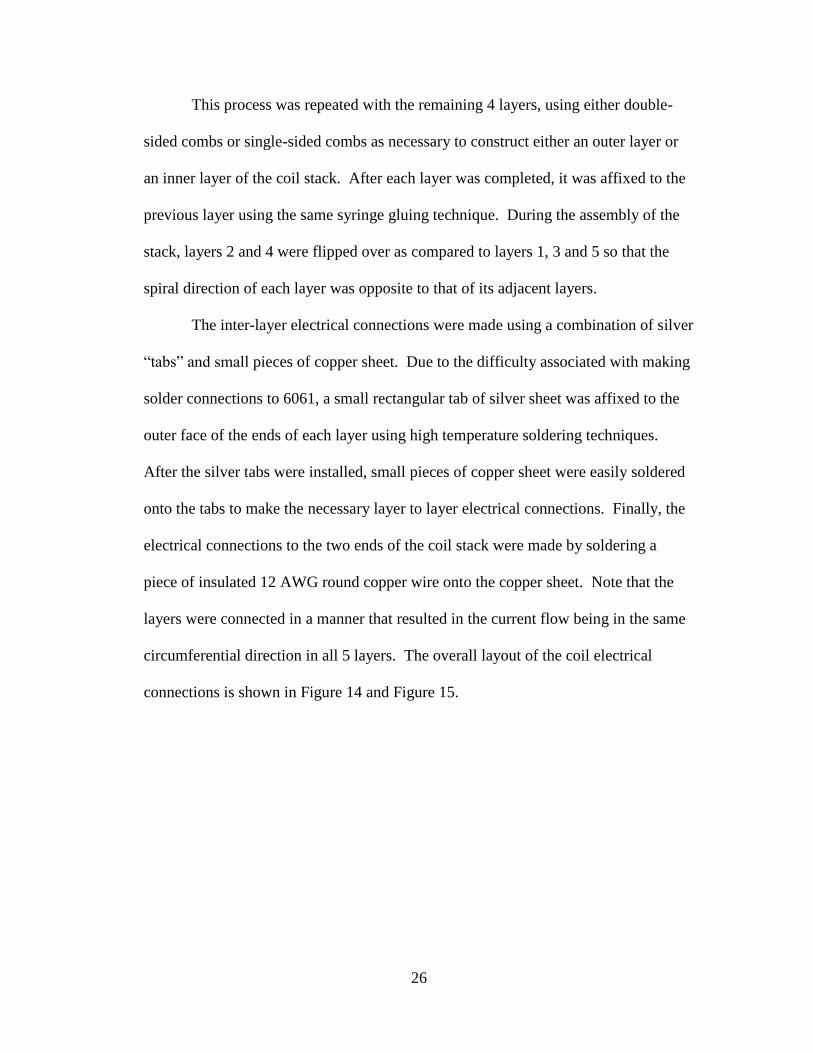
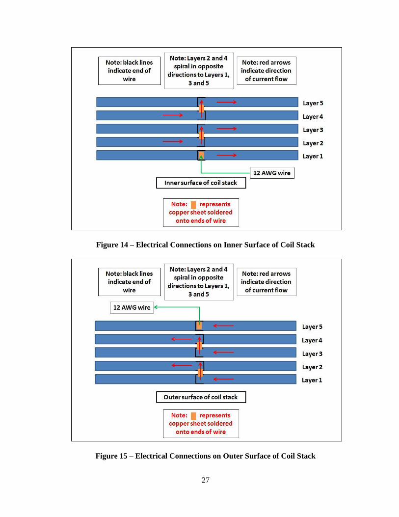
This process was repeated with the remaining 4 layers, using either double-
sided combs or single-sided combs as necessary to construct either an outer layer or
an inner layer of the coil stack. After each layer was completed, it was affixed to the
previous layer using the same syringe gluing technique. During the assembly of the
stack, layers 2 and 4 were flipped over as compared to layers 1, 3 and 5 so that the
spiral direction of each layer was opposite to that of its adjacent layers.
The inter-layer electrical connections were made using a combination of silver
“tabs” and small pieces of copper sheet. Due to the difficulty associated with making
solder connections to 6061, a small rectangular tab of silver sheet was affixed to the
outer face of the ends of each layer using high temperature soldering techniques.
After the silver tabs were installed, small pieces of copper sheet were easily soldered
onto the tabs to make the necessary layer to layer electrical connections. Finally, the
electrical connections to the two ends of the coil stack were made by soldering a
piece of insulated 12 AWG round copper wire onto the copper sheet. Note that the
layers were connected in a manner that resulted in the current flow being in the same
circumferential direction in all 5 layers. The overall layout of the coil electrical
connections is shown in Figure 14 and Figure 15.
27
Figure 14 – Electrical Connections on Inner Surface of Coil Stack
Figure 15 – Electrical Connections on Outer Surface of Coil Stack

28
2.3: Electrical Testing and Characterization
The AC current flowing through a single winding of the coil will induce eddy
currents in the neighboring windings of the coil. These eddy currents cause the
impedance of the coil to change with frequency. More specifically, the coil’s
resistance increases at higher frequencies and its inductance decreases at higher
frequencies. These frequency dependent effects are commonly referred to as the
proximity effect. An analytical approximation for predicting the AC behavior of
coils, known as Dowell’s method, is presented in [7].
To measure the effect of increasing frequency on coil resistance and
inductance, test capacitors (also called loading capacitors) of various values were
connected in series with the coil. The experimental test setup is shown in Figure 16.
Two Fluke 87V multimeters were utilized – one connected in series with the load to
measure the load current IL, and the other connected across the load to measure the
load voltage VL. This two-multimeter arrangement allowed for calculating the load
impedance as VL / IL. For each test capacitor value, the resonant frequency was
determined by locating the frequency of minimum load impedance. It should be
noted that due to changes in R and L with frequency, the point of minimum load
impedance is not guaranteed to be the point of zero reactance, and hence the
minimum load impedance may not be purely resistive. However, as will be shown
later, for the frequency ranges used in our tests, a numerical analysis shows that the
difference between the minimum impedance and the impedance at zero reactance is
less than 4%. We therefore assume that the minimum impedance measured is in fact
the AC resistance of the coil at each frequency.

29
Figure 16 – Test Setup for Measuring Proximity Effect
Another source of possible error in this setup is dielectric losses in the
capacitors themselves. However, all loading capacitors used were film capacitors
with a metallized polypropylene dielectric. Due to the extremely low dissipation
factor of this dielectric, the predicted equivalent series resistance (ESR) for each
loading capacitor was less than 1% of the measured load impedance, so these losses
were neglected.
The measured AC resistance of the coil at different frequencies is shown in
Figure 17. Also shown is the AC resistance as calculated by the Dowell method. The
Dowell method equation for resistance is
(7)
where M’ and D’ are the real parts of M and D, respectively, with M and D given by
(8)
and

30
(9)
with
(10)
Note that the notation used here matches that presented in Table 1.
It is clear (see Figure 17, below) that the Dowell method significantly under-
predicts AC resistance for our coil cross section. This could be due to the fact that
our rectangular conductor has a high aspect ratio a/h, and the Dowell method is better
suited for square conductors. Furthermore, the gap between successive turns, u, is not
insignificant in comparison to the height of the conductor, h (they are in fact equal),
which could be introducing additional errors. As stated in [8], one classical approach
to deal with this air gap is to increase the conductor height so that the air gap is
eliminated and modify the resistivity such that the DC resistance of the coil remains
the same. Making this modification requires us to double the value of h and double
the value of . As seen in Figure 17, the modified Dowell method is closer to the
experimentally measured values, but still under-predicts the AC resistance.

31
Figure 17 – Frequency Dependent Behavior of Coil Resistance
The capacitance of each test capacitor was also measured with a Fluke 87V
multimeter. With these capacitance measurements, it was possible to calculate the
coil inductance at each resonant frequency. These AC inductance values are plotted
in Figure 18. Dowell’s method also provides a prediction for coil inductance versus
frequency, which is given as the sum of two components. The first component, LU, is
the contribution from the gap between layers and is frequency independent. The
second component, L, is called the AC leakage inductance and is dependent on
frequency. The Dowell method equation for inductance is
(11)
where M’’ and D’’ are the imaginary parts of M and D, respectively.

32
Total coil inductance, LU + L, is plotted in Figure 18. We can see that while
the DC inductance LU predicted by Dowell’s method is lower than what was
determined experimentally, the measured data does follow the predicted trend
somewhat qualitatively. However, the Dowell method does not predict any
significant decrease in inductance until 10 kHz, whereas the measured values start to
show an inductance decrease beginning around 1 kHz.
Figure 18 – Frequency Dependent Behavior of Coil Inductance
Since we expect the measured data to follow a Dowell-like trend at least
qualitatively, a “Dowell method curve fit” was applied to the experimental data for
resistance and inductance. The two curve fits follow the Dowell method equation
forms given in equations (7) and (11). For the resistance fit, the number of layers was
set to 20 and and h were set as the free parameters. For the inductance fit, the
number of layers was again set to 20 and , h, LU, and L were set as the free
parameters. Both curve fits, shown in Figure 19 and Figure 20 below, match the data
well and have an R2 value greater than 0.99.

33
Figure 19 – Curve Fit Applied to Measured Resistance Data
Figure 20 – Curve Fit Applied to Measured Inductance Data
As mentioned earlier, the dependence of R and L on frequency can
theoretically lead to a discrepancy between the frequency of minimum impedance and
the frequency of zero reactance. Using the curve fits for resistance and inductance, a
MATLAB script was written to numerically calculate the magnitude of this
discrepancy. The script loops over a frequency range of 1 Hz to 8 kHz in 1 Hz
increments. The procedure for each loop iteration is then as follows:

34
1. Given a frequency f, use the inductance curve fit to calculate the AC
inductance of the coil at that frequency. Then, calculate the capacitance C
required to make f the zero-reactance frequency of the system, given by
(12)
where we have called the AC inductance result from the curve fit LZR, as this
is the value of the coil’s inductance at the frequency of zero reactance.
2. Create an additional frequency sweep vector fsweep which has a range of 0.5*f
to 1.5*f.
3. Use the inductance and resistance curve fits to calculate LAC and RAC at each
point in fsweep.
4. Calculate the impedance at each point in fsweep by
(13)
5. Numerically locate the frequency in fsweep at which the impedance is
minimum. This value is the minimum impedance of the circuit, called ZMinZ.
6. At the frequency corresponding to ZMinZ, use our inductance and resistance
curve fits to calculate the inductance at minimum impedance, called LMinZ,
and the resistance at minimum impedance, called RMinZ.

35
The results of the investigation are shown in Figure 21. The solid blue line
represents the discrepancy between the value of minimum impedance, ZMinZ, and the
AC resistance of the coil, RMinZ, at the same frequency. Up to 8 kHz, which was the
highest measured frequency, the difference is less than 4%, so we conclude that it is
sound to assume that the measured values of minimum impedance are equal to the
AC coil resistance. The dashed red line represents the discrepancy between the coil
inductance at minimum impedance, LMinZ, and the coil inductance which corresponds
to zero reactance, LZR. At frequencies less than 8 kHz, the difference is less than
1.5%, so we also proceed with the assumption that the measured inductance values
are accurate.
Figure 21 – Comparison of Minimum Impedance and Zero Reactance for
Resonant Coil Circuit
36
Chapter 3: Housing and Interior Components
3.1: Housing Design
3.1.1: Structural Requirements and Design
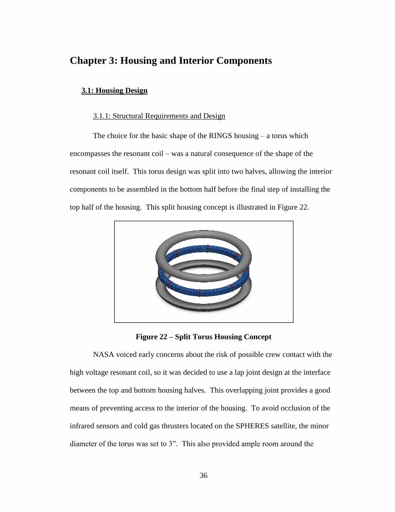
The choice for the basic shape of the RINGS housing – a torus which
encompasses the resonant coil – was a natural consequence of the shape of the
resonant coil itself. This torus design was split into two halves, allowing the interior
components to be assembled in the bottom half before the final step of installing the
top half of the housing. This split housing concept is illustrated in Figure 22.
Figure 22 – Split Torus Housing Concept
NASA voiced early concerns about the risk of possible crew contact with the
high voltage resonant coil, so it was decided to use a lap joint design at the interface
between the top and bottom housing halves. This overlapping joint provides a good
means of preventing access to the interior of the housing. To avoid occlusion of the
infrared sensors and cold gas thrusters located on the SPHERES satellite, the minor
diameter of the torus was set to 3”. This also provided ample room around the

37
resonant coil for wire routing and the placement of interior components. A
conceptual cross section of the two housing halves encompassing the resonant coil is
shown in Figure 23.
Figure 23 – Cross-Sectional View of Housing Halves and Resonant Coil
Due to the high costs associated with manufacturing the housing via injection
molding, it was decided instead to use vacuum forming techniques. In vacuum
forming, a flat sheet of plastic material is heated to a temperature at which it is pliable
and then lowered around a mold. A vacuum is then created between the sheet and the
mold, drawing the plastic into the desired shape. As a consequence of this
manufacturing method, the part must be designed with uniform thickness throughout.
Additionally, the finished part may exhibit localized thinning of the plastic in areas of
high deformation. Also, the final part will have a much better tolerance on the side of
the plastic which is in contact with the mold. To ensure a tight tolerance at the lap
joint, the housing bottom was made on a female mold and the housing top was made
on a male mold. This ensured that the exterior surface of the housing bottom and the
interior surface of the housing top both had tight tolerances, producing a good fit at
the lap joint.

38
NASA encouraged the use of polycarbonate for the housing material due to its
low outgassing properties and its high resistance to impact and fracturing. To
determine the necessary housing thickness, a finite element analysis (FEA) simulation
was performed for two different static loading scenarios. For simplicity, the housing
in both analyses was modeled as a hollow, one-piece torus, and the simulations were
carried out using SolidWorks Simulation.
The first loading scenario, known as the “push-off load,” was based on a
NASA requirement. This setup is representative of the loads created when a crew
member pushes on the housing while it is attached to an ISS wall for stowage. The
requirement nominally calls for an application of 125 lbf over an area of 4 in2.
However, due to the curvature of the housing wall, this load was applied over a 2” x
1” rectangle located on the top face of the housing, as this was more representative of
the actual contact area in a push-off scenario. An annulus having a thickness of 0.25”
and located on the opposite face of the housing was used as the constrained area, as it
was felt this was a good approximation for the contact area between the RINGS
housing and the ISS wall. The loading setup and results of the FEA simulation are
shown in Figure 24. With a shell thickness of 0.080”, the minimum factor of safety
(FOS) based on the yield strength of polycarbonate was found to be greater than 2.

39
Figure 24 – FEA Analysis of Push-off Loading Scenario
The second FEA analysis is known as the “pick up quickly” loading scenario
and is more applicable to the handling of the housings before launch than it is to
operations on the ISS. This setup is representative of a situation in which the housing
is picked up with two hands and swiftly accelerated upwards. Two 45 lbf loads were
each applied over a 1” x 1” area, and these two areas were diametrically opposed to
one another on the underside of the torus. These loads are a highly conservative
estimate that model the resonant coil as dead mass under a 2.5g acceleration. Two
diametrically opposed constraints were also placed on the underside of the torus,
having an area of 1” x 1”. The loading setup and results of the FEA simulation are
shown in Figure 25. With a shell thickness of 0.080”, the minimum FOS based on
the yield strength of polycarbonate was found to be greater than 6.

40
Figure 25 – FEA Analysis of Pick Up Quickly Loading Scenario
It should be noted that both of these loading scenarios are overly conservative
since the interior components of the housing provide additional structural rigidity.
Using these results, a housing thickness of 0.125” was chosen, which is a readily
available size for polycarbonate sheets. It was estimated that localized part thinning
could reduce this thickness to as low as 0.080” in some places, which was deemed
acceptable based on our FEA results for a 0.080” thick housing.
3.1.2: Cooling Requirements and Thermal Design
The next step in designing the housing was a thermal analysis used for the
sizing of the cooling fans. At the maximum design current of 18 amps RMS, the
predicted power dissipation in the coil was calculated to be approximately 315 watts.
Due to the absence of natural convection in the microgravity environment onboard
the ISS, all of this power must be removed via forced convection using fans. It was
assumed the temperature of the entering air was 75°F (24°C) and a nominal exit air
temperature of 100°F (38°C) was prescribed. NASA requirements dictated that the

41
exiting air have a temperature less than 115°F, so this choice provided additional
margin. The power required to increase the temperature of the air is then given by
(14)
where is the air mass flow rate in kg/s, cp is the specific heat capacity of air at
constant pressure in J/(kg∙K), and ΔT is the difference between the temperature of the
entering air and exiting air in °C. The required mass flow rate is then
(15)
Assuming an air density of 1.10 kg/m3, which is slightly lower than the density of air
at 38°C to provide additional margin, the corresponding volumetric flow rate is
(16)
With the necessary volumetric flow rate calculated to be 42 cubic feet per
minute (CFM), the NMB 1604KL-04W-B50-B00 fan was selected. This box shaped
fan produces a nominal flow rate of 6 CFM and has dimensions of 40mm x 40mm x
10mm. This small size and thin profile allowed for easy integration into the housing
wall. From the energy analysis, only 7 fans are required, but it was decided to
include 10 fans to provide additional margin. Eight of these 10 fans are located on
the outer surface of the housing, spanning the joint between the two housing halves.
The remaining two fans are located on the oblique walls of the “powerbox” area of
the housing, which is discussed in more detail in Section 3.1.3. A conceptual
overhead view of the fan locations is shown in Figure 26.

42
Figure 26 – Fan and Diffuser Locations
Also shown in Figure 26 are the locations of the four exit air diffusers. The
diffusers are located on the inner face of the torus and consist of a simple matrix of
drilled holes, as shown in Figure 27. By placing them on the inner face, the exiting
air impinges on the SPHERES satellite. This is advantageous because the net
momentum gain from the exiting air is zero, eliminating a possible source of error
from EMFF operations. Additionally, the exit air diffusers are offset from the outer
fan locations so that the cooling air is forced to travel some distance in the
circumferential direction within the housing, which serves to improve the cooling of
the resonant coil.
43
Figure 27 – Exit Air Diffuser
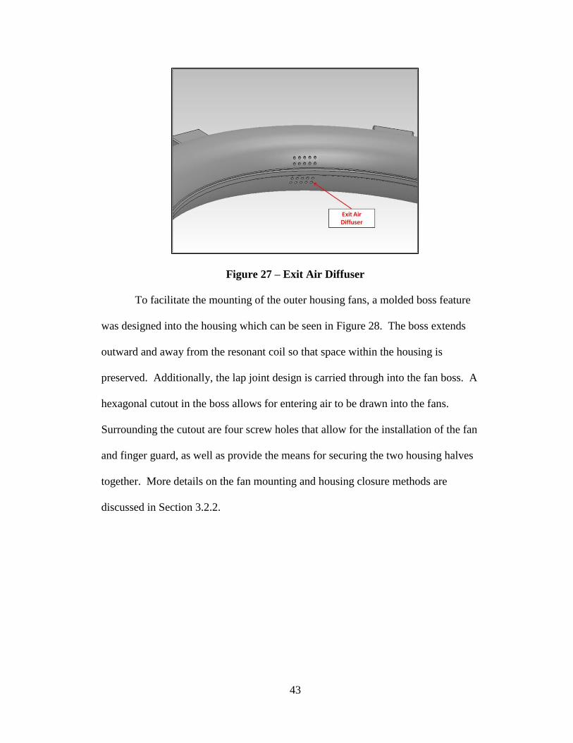
To facilitate the mounting of the outer housing fans, a molded boss feature
was designed into the housing which can be seen in Figure 28. The boss extends
outward and away from the resonant coil so that space within the housing is
preserved. Additionally, the lap joint design is carried through into the fan boss. A
hexagonal cutout in the boss allows for entering air to be drawn into the fans.
Surrounding the cutout are four screw holes that allow for the installation of the fan
and finger guard, as well as provide the means for securing the two housing halves
together. More details on the fan mounting and housing closure methods are
discussed in Section 3.2.2.

44
Figure 28 – Outer Fan Boss
3.1.3: Electronics Box
With the torus diameter and housing cross section dimensions finalized, our
colleagues at Aurora Flight Sciences (AFS) proceeded to design the RINGS to
SPHERES support structure. The support structure consists of four struts, four cuffs,
and a mating sleeve. Each of the four struts extend radially outward from the mating
sleeve and attach to a cuff. The cuffs are made from two halves in the same manner
as the RINGS housing. After the housing top is installed, the top cuff is bolted to the
bottom cuff and to the strut. The support structure assembly is shown with a
SPHERES satellite installed in Figure 29. For reference, the SPHERES satellite is
shown in blue, the mating sleeve in red, the four struts in black, and the four cuffs in
yellow.

45
Figure 29 – Support Structure and SPHERES Satellite
Also shown in Figure 29 are the two RINGS batteries installed into their
battery mounts. These batteries, part number DC9180 made by DeWalt, have a
nominal output voltage of 18 volts and a capacity of 2.2 amp-hours. Located opposite
the two battery mounts is the SPHERES expansion port interface, which RINGS
connects two with a 50 pin cable to facilitate communication between RINGS and
SPHERES. The “powerbox” portion of the housing, which provides space for the
46
RINGS electronics, was placed in the quadrant nearest the expansion port for two
reasons. First, having the powerbox near the expansion port meant that the
SPHERES to RINGS communication cable would not have to be undesirably long,
making the installation of this cable easier for the RINGS operators. Additionally,
since the batteries shift the center of mass of the assembly away from its geometric
center, placing the RINGS electronics opposite them helps to bring the center of mass
back closer towards the center of the satellite.
The powerbox was designed to provide the maximum possible volume within
its quadrant. However, a gap of just over 1.5” was left between the powerbox and the
expansion port to allow for the installation of the communications cable. A similar
sized gap was left between the two struts and the oblique walls of the powerbox to
provide room for strut installation and clearance for the two fans located on the
oblique walls of the powerbox. The height of the powerbox was set to 3”, the same
as the height of the torus cross section, so as not to occlude the infrared or ultrasound
sensors on the SPHERES satellite. To accommodate the installation of various
electronic components, several cutouts were designed into the face of the powerbox.
The final design of the RINGS housing, attached to the support structure, is shown in
Figure 30.

47
Figure 30 – Final Design of RINGS Housing Attached to Support Structure
3.2: Interior Component Design
3.2.1: Mounting the Resonant Coil
The resonant coil is secured within the housing using a series of polycarbonate
parts known as “comb supports.” As shown in Figure 31, the comb support has a
curved surface on its underside which is machined to the same radius as the housing

48
wall. On the top surface, a groove is designed to capture the portion of the single
sided combs that extend above and below the outer layers of the resonant coil. In
addition, a cut through the center of the underside of the part provides an area for
routing various wires within the housing.
Figure 31 – Comb Support
Eight of these comb supports are glued into each housing half, for a total of 16
per RINGS vehicle. The adhesive used is Permabond 820, the same as was used for
attaching the combs to the resonant coil wire. An exploded and collapsed view of the
comb support setup is shown in Figure 32, with the comb supports shown in yellow
for clarity.

49
Figure 32 – Comb Support Setup
3.2.2: Flow Guide Fins
There are two types of “flow guide fins” installed in the RINGS housing:
inner fins and outer fins. The fins serve two purposes. First, they act as a physical
barrier between the airflow cutouts in the housing and the high voltage resonant coil.
More specifically, they prevent line of sight access to the resonant coil through the
outer housing fan cutouts and the exit air diffuser holes. This prevents the operators
from contacting the resonant coil with a finger or a tool such as a screwdriver. The
second purpose of the fins is to control the flow direction of the cooling air inside the
housing to enhance cooling performance.
The inner fins are curved pieces made from 1/16” thick polycarbonate sheet.
Three identical inner fins, which are mounted to four inner fin mounts, are used in the
housing to block access to the resonant coil through the exit air diffusers. An inner
fin and an inner fin mount are shown in Figure 33. The inner fin mounts are also
made from polycarbonate, and they are glued to the bottom half of the housing using

50
Permabond 820. The curved face on the back of the inner fin mounts matches the
curvature of the housing wall, and the small flat portion of this curved face mates to
the flat section at the top of the housing bottom to ensure they are accurately located
during installation. The front of the inner fin mount features a flat face to which the
ends of the inner fins are adhered with Permabond 820. Additionally, a cutout
through the center of the inner fin mount provides an area for wire routing.
Figure 33 – Inner Flow Guide Fin and Inner Fin Mount
The three inner fins are mounted end to end in the housing, as shown in the
exploded and collapsed views in Figure 34. Though small, the inner fin mounts can
be seen in the left image of Figure 34, where they are displayed already mounted to
the housing bottom.
Figure 34 – Inner Fin Setup

51
The outer fins are similar to the inner fins and are also made from 1/16” thick
polycarbonate sheet. A total of eight outer fins are used in the housing to prevent
access to the resonant coil through the outer fan inlets. As opposed to the inner fins,
which are curved into shape using a heating process before installation, the outer fins
are straight pieces. By joining the eight outer fins end to end into a ring, the pliable
fins are curved into their appropriate shape. An outer fin and the assembled outer fin
ring are shown in Figure 35.
Figure 35 – Outer Fin and Outer Fin Ring
There are a total of eight end to end joints in the outer fin ring. Four of these
joints are held together with a small polycarbonate piece. Two #4-40 stainless steel
screws and two steel nuts with nylon inserts (for back-out prevention) are used to
hold the outer fin joint to the outer fins. The remaining four joints are connected
using an infrared sensor (IR) board. The same screws are used to mount the IR board,
but two 1/8” long steel spacers are included to provide clearance for the surface
mount components located on the rear side of the IR board. Figure 36 shows the two
different types of outer fin joint connections.

52
Figure 36 – Outer Fin Joint Connections
Once assembled, the outer fin ring is placed into the housing as shown in
Figure 37. Note that no glue is used to install the outer fin ring. Rather, it is held in
place by the outer housing screws which also serve to hold the outer fins in place and
to attach the housing top to the housing bottom.
Figure 37 – Outer Fin Setup
In the center of each outer fin are four screw holes. A #4-40 stainless steel
screw is inserted through each screw hole from the inner face of the fin and threaded
into a #4-40 threaded polycarbonate standoff. Next, a 1/8” long #4-40 nylon set
screw is threaded into the standoff through the open end. The fans are then placed in
the housing. The outer end of the standoffs sit inside four recesses on the inner face

53
of the fans, preventing the outer fin ring from rotating in the circumferential direction
and properly locating the outer fans in the housing. Finally, after the housing top is
installed, four #4-40 stainless steel screws are inserted through the steel finger guards,
the housing screw holes, and the fan screw holes, and are then threaded into the open
end of the polycarbonate standoff. An exploded view of this design is shown in
Figure 38.
Figure 38 – Outer Fan Mounting Setup
Polycarbonate and nylon were used for the standoffs and set screws to provide
electrical insulation between the inner screw head and outer screw head. In the
unlikely event that the inner screw head contacts the resonant coil, this design
guarantees that the outer screw head, which is accessible to the crew, is well insulated
from the resonant coil. For back-out prevention, both the inner screws and outer
screws have a nylon locking patch on their threads. A cross-sectional view of the
entire outer fan mounting setup is shown in Figure 39.

54
Figure 39 – Cross-Sectional View of Outer Fan Mounting Setup
As mentioned earlier, the inner and outer fins also function as flow guide
devices. Both fin types are designed such that their top and bottom surfaces sit flush
against the inner face of the housing, forming a seal. This can be seen in Figure 40,
which is a cross-sectional view with the cut made through a comb support location.
For clarity, the outer and inner fins are shown in black, the inner fin mount in green,
the comb supports in yellow, the combs in red, and the resonant coil in blue.

55
Figure 40 – Comb Support Cross-Sectional View
Because the top and bottom edges of the fins sit flush against the inner wall of
the housing, a “cooling channel” is formed around the resonant coil. An added
benefit of this setup is that wiring which runs from the powerbox to components
located at a distance from it, such as the IR boards and outer fans, can be routed in the
two cavities formed on either side of the channel. This setup ensures that this wiring
is safely isolated from the high voltage, high temperature resonant coil.

56
Figure 41 – Resonant Coil Cooling Channel
All inner and outer fins have a notch cut into their center to allow cooling air
to pass through. As can be seen in Figure 33 and Figure 35, the inner fin notch is
placed at the bottom of the fin, and the outer fin notch is placed at the top of the fin.
Based on the locations of the outer fin notches, the cooling air is forced to pass up and
over the top of the outer fins, so that it contacts the top layer of the resonant coil first.
Similarly, to exit the housing the cooling air must pass through the bottom notch
locations of the inner fins, below the bottom layer of the resonant coil. Figure 42
shows the fin notch locations in more detail. This notch design forces the cooling air
to pass through all five layers of the resonant coil, enhancing thermal performance.
Without the notches, the majority of the airflow would most likely travel completely
over or under the resonant coil, without much flow penetration into the core of the
windings.

57
Figure 42 – Outer and Inner Fin Notch Locations
3.2.3: Powerbox Fans
In addition to the eight outer housing fans, two fans are located on the oblique
walls of the powerbox area of the housing. The powerbox fans are enclosed in a
polycarbonate part called a “fan box.” An image of a fan box is shown in Figure 43.
Two mounting grooves are located on the top and bottom edges of the fan box to
allow it to be mounted in the housing walls.
Figure 43 – Fan Box

58
Four #4-40 screws and four nylon insert nuts are used to secure the fan inside
the fan box. These screws also secure the fan guard to the outside of fan box. To
prevent line of sight access through the fan inlet and into the powerbox, a “fan box
plug,” also made from polycarbonate, is adhered to the inner face of the fan box using
Permabond 820. Similar to the outer fins, the fan box plug forces the cooling air to
flow upwards and exit the fan box near the top of the powerbox. The fan box
assembly is shown in Figure 44.
Figure 44 – Fan Box Assembly
As mentioned earlier, two mounting grooves on the top and bottom faces of
the fan box facilitate their mounting into the housing wall. This setup is shown in
Figure 45. First, the fan boxes are placed into the housing bottom with the housing
wall occupying the bottom groove of the fan box. Then, as the housing top is
installed, its wall slides into place in the top groove of the fan box, which securely
traps the fan box in place.

59
Figure 45 – Fan Box Mounting
. While access into the housing through the three exit air diffusers on the
curved surfaces of the housing is blocked by the three inner fins, the diffuser on the
powerbox is blocked by a separate component. Made from polycarbonate, the
“diffuser safety cap” is shown in Figure 46. Two flanges on either side of the diffuser
safety cap contain screw holes which allow it to be mounted to the housing top.
Figure 46 – Diffuser Safety Cap
The diffuser safety cap is mounted to the housing top using two #4-40 screws
with nylon insert nuts. Once the housing top is installed, it properly blocks access
into the powerbox through the exit air diffuser. This setup is shown in cross-sectional
views in Figure 47. Only the bottom face of the safety cap is open, so that once it is
installed, the cooling air can only exit the diffuser by traveling up into the diffuser

60
from the bottom of the housing. Since the fan box plugs force the air to enter the
powerbox at the top of the housing, cooling performance is enhanced since the air
must travel down through the powerbox before exiting, similar to the notch setup in
the outer and inner fins.
Figure 47 – Diffuser Safety Cap Setup

61
Chapter 4: Electronics
4.1: Circuit Design
4.1.1: Resonant Coil Drive Circuit
At the heart of the RINGS electronics is the resonant coil drive circuit, which
must convert the DC voltage of the batteries into an AC voltage to be applied to the
load. A drive architecture based upon a high power operational amplifier (op amp)
was considered, but due to the high currents that were needed in the coil, the power
dissipated in the op amp would have been unmanageably large. It was estimated that
the power dissipated in an op amp would be at least 150 watts, which would have
been too much of a thermal burden, in addition to significantly reducing the battery
depletion time due to the extra power draw.
Since the op amp was not a viable option, it was decided instead to use an H-
Bridge architecture. An H-Bridge uses four metal-oxide-semiconductor field-effect
transistors (MOSFETs) in a switching configuration. By rapidly switching these
transistors in a controlled manner, an AC voltage having a rectangular waveform can
be produced from a DC voltage source. Since the MOSFETs have an extremely low
resistance in their “on” state, power dissipation in the H-Bridge is drastically lower
than in an op amp. In addition, another benefit of the H-Bridge setup is the ability to
precisely control both the frequency and duty cycle of the applied voltage. One
drawback of using the H-Bridge architecture is the presence of higher frequency
harmonics in the rectangular wave AC voltage. These harmonics slightly increase the
power dissipated in the resonant coil; however, the total power dissipated in the drive

62
circuit and resonant coil is significantly lower with the H-Bridge setup than it would
be with an op amp architecture.
It was decided to use a commercial off-the-shelf (COTS) H-Bridge circuit
board made by Robot Power. Known as the open source motor controller (OSMC),
the board is marketed as a high current motor controller for use in robot combat. The
OSMC features many built in safety devices and is designed to avoid the common
problems encountered in H-Bridge circuit design. It has a maximum continuous
current rating of 160 amps and a maximum source voltage rating of 50 volts, both of
which are higher than is necessary for the RINGS drive circuit. A picture of the
OSMC is shown in Figure 48.
Figure 48 – Open Source Motor Controller (OSMC) made by Robot Power
The resonant coil can be modeled as an inductor and resistor in series. By
adding a capacitor in series with the coil, the load becomes a series RLC circuit.
Since RINGS operates at two different resonant frequencies (one for EMFF mode and
one for WPT mode), two different amounts of capacitance must be added to the coil

63
depending on the operational mode selected. Additionally, a load resistor must be
connected in series with the coil in WPT Receive mode. To achieve this three mode
operational capability, the drive circuit was designed as is shown in Figure 49.
Figure 49 – RINGS Drive Circuit Schematic
In Figure 49, the four MOSFETs of the H-Bridge are labeled as AHI, ALO, BHI,
and BLO. The resonant coil is represented by L and R, and CE and CW are the
capacitors utilized in EMFF and WPT modes, respectively. The load resistor
necessary for WPT Receive mode is shown as RL. Finally, two relays are included as
well as a group of three current sensors. By toggling the two relays, three different
operational modes can be achieved, as summarized in Table 2. The last column in
Table 2 shows the actual resonant frequencies of the completed RINGS units. All

64
four RINGS units which have been built are extremely well matched and exhibit less
than 1 Hz (which is the maximum resolution of the commanded frequency) of
resonant frequency difference for both EMFF and WPT Transmit operational modes.
Table 2 – Drive Circuit Operational Modes
Operational Mode
Relay 1 Relay 2 RLC Capacitance Resonant Frequency (Hz)
WPT Transmit Open Open CW (10 F) 462
WPT Receive Open Closed CW (10 F) 462
EMFF Closed Open CW + CE (310 F) 83
In EMFF and WPT Transmit modes, the H-Bridge MOSFETs are actively
switched to apply the AC voltage to the load. In WPT Receive mode, the H-Bridge
MOSFETs are disabled and a 2 ohm load resistor with a maximum power rating of 70
watts is connected in series with the resonant coil. The rationale for setting the load
resistor value at 2 ohms is discussed in Section 5.1.2, and the choice of 462 Hz for the
WPT operating frequency is discussed in Section 5.1.1.
Because the proximity effect causes increased resistance and hence higher
power dissipation at higher frequencies, it was sought to make the EMFF operational
frequency as low as possible. Due to the high currents involved, it was necessary to
use capacitors made from metallized polypropylene, a dielectric with a low loss
tangent, to prevent the capacitors from overheating. Capacitors made of these high
quality film dielectrics are, unfortunately, quite a bit larger than other capacitor
chemistries. As a result, the EMFF capacitor selection was ultimately governed by
available space within the powerbox. The best available option was to use two 150
µF capacitors in parallel for the EMFF capacitance. In EMFF mode, these two
capacitors are connected in parallel with the 10 µF WPT capacitor via Relay 1 as

65
shown in Figure 49. The total of 310 µF utilized in EMFF mode sets the resonant
frequency of the RLC circuit to approximately 83 Hz.
In addition to safely handling the large currents, the resonant circuit capacitors
must also be able to withstand the large voltages associated with a resonant circuit.
At resonance, the energy in the circuit oscillates back and forth between the inductor
and the capacitor. This allows us to write an energy balance equation for the inductor
and capacitor as
(17)
where L is the inductance of the coil, I is the peak value of the current through the
coil, C is the added capacitance, and V is the peak voltage seen across the capacitor.
In EMFF mode, the values are: L = 11.9 mH, I = 18 amps RMS = 25.5 amps peak,
and C = 310 µF. This results in a maximum AC voltage across the EMFF capacitors
of 158 volts peak. To provide margin, the selected EMFF capacitors have a voltage
rating of 600 volts peak. The currents generated in WPT Transmit mode are lower
than 18 amps RMS, due to the higher resistance of the coil at the WPT frequency, as
well as the need to stay safely beneath the power dissipation limits of the WPT
capacitor. The onboard microcontroller, discussed in more detail in Section 4.1.2,
monitors the current while in WPT transmit mode to ensure that a current limit of 15
amps RMS is not exceeded. The WPT mode parameters are therefore L=11.9 mH, I
= 15 amps RMS = 21.2 amps peak, and C = 10 µF. This results in a maximum AC
voltage across the WPT capacitor of 732 volts peak. To provide margin, the selected
WPT capacitor has a voltage rating of 1300 volts peak.

66
At the EMFF operational frequency of 83 Hz, the results from the
experimental characterization of the proximity effect indicated a coil resistance of
approximately 1.1 ohms. Since the DeWalt batteries present a voltage as low as 15
volts when they are near depletion, connecting them in parallel would not allow for
achieving the goal current of 18 amps RMS in the resonant coil. Accordingly, the
decision was made to connect the batteries in series so that even when they are nearly
depleted, 18 amps RMS can still be achieved.
Relay selection was governed by the maximum current and voltage that the
relays have to withstand. In EMFF mode, Relay 1 must be able to carry 18 amps
RMS. As previously stated, the maximum voltage that the WPT capacitor will see is
approximately 732 volts peak. Since Relay 1 is open when in WPT transmit mode,
all 732 volts are dropped across the open relay contacts. The K41A734 relay was
selected, a single pole single throw normally open (SPST-NO) model manufactured
by TE Connectivity. It features a maximum current rating of 30 amps DC and a
maximum contact voltage rating of 5 kilovolts, both of which are well in excess of the
RINGS design parameters. For simplicity, the same relay was used for both Relay 1
and Relay 2, even though Relay 2 did not require quite as high of a current and
voltage rating.
4.1.2: Low Power Board
With the resonant coil drive circuit design finalized, the next step was the
design of the “low power board.” The low power board contains a PIC
microcontroller, various voltage regulators to supply power to sensors, integrated
circuits (ICs) and other components, several op amps used for signal conditioning, a

67
pair of battery protection diodes, the low battery detection circuit, and a set of logic
gates. Off-board components that connect directly to the low power board include
two liquid-crystal displays (LCDs), a pair of low battery indicator light-emitting
diodes (LEDs), a single “master clear” pushbutton used for resetting the PIC, two
pushbuttons used for toggling the display mode of the LCDs, and two temperature
sensors.
The microcontroller selected for RINGS is part number PIC32MX340F512H,
manufactured by Microchip. Among its many features are several analog and digital
inputs, multiple digital outputs, an 80 MHz primary oscillator, and a universal
asynchronous receiver/transmitter (UART) port, all based around a 32-bit core
processor. The analog inputs are used to read in data from three Hall Effect current
sensors, a pair of RMS-to-DC converter ICs, and two temperature sensors. Signals
read in via the digital inputs include the IR sensor trigger, the low battery signal, the
LCD pushbutton signal, and the PIC master clear pushbutton signal. In addition, the
Hall Effect current sensors have a “fault” pin that transitions from 5 volts to ground in
the event of an “overcurrent” scenario (more information on the overcurrent fault can
be found in Section 4.1.3). These three fault signals, as well as the result from a logic
gate voting scheme, are read into the PIC via its digital inputs. The digital outputs are
used to send control signals to the OSMC which set the duty cycle and frequency of
the voltage applied to the resonant coil circuit, relay state command signals to set the
proper operational mode, and signals used for commanding the two LCDs. Three
additional digital out pins connect to “fault enable” inputs on the Hall Effect current
sensors, which are used to activate or deactivate their fault sensing capability. The

68
UART port allows for communications with the SPHERES satellite. Through this
port, RINGS periodically sends test data such as the current waveform in the resonant
coil and the temperature of the exiting air and the coil. The primary data sent from
SPHERES to RINGS is the desired magnitude and phase of the coil current, which
the PIC then translates into an appropriate duty cycle and phase angle to achieve the
desired current.
The low power board contains a total of five voltage regulators. Two of these
regulators provide a 12 volt output which is used for powering the ten cooling fans
and for actuating the two relays. Because of the noise produced by the fans, the outer
housing fans are only turned on when the drive circuit is operating and current is
circulating in the coil. The two powerbox fans, however, are always turned on when
the RINGS power switch is in the on position. To achieve this outer housing fan
toggling capability, the first 12 volt regulator is used solely to power those eight fans,
and features an on/off signal input which is commanded by a PIC digital output. The
second 12 volt regulator is connected to the two powerbox fans and is also used to
actuate the relays when the relay circuits are commanded by the PIC digital outputs.
Since the current required for powering the fans and relays is higher than that
required for the rest of the components, the two 12 volt regulators have a switching
architecture to reduce power dissipation. The other three voltage regulators, however,
are linear regulators. The first of these three regulators supplies the necessary 3.3
volts to the PIC. The other two voltage regulators have a 5 volt output, which is used
for powering various logic gates, op amps, and sensors, as well as the two LCD
backlights.

69
Also contained on the low power board are five op amps that are used for
signal conditioning. The first three of these op amps modify the output from the three
Hall Effect current sensors. The output from the current sensors is an AC voltage
signal proportional to the AC coil current, with a DC offset of 2.5 volts. Since the
analog inputs on the PIC only have a range of 0-3.3 volts, it was desired to reduce the
DC offset in the current sensor signal from 2.5 volts to 1.65 volts so that it was
centered within the read-in range. This offset shift is achieved using an LT1077 op
amp with the layout shown in Figure 50. In Figure 50, VHE1 is the output signal
from the first Hall Effect current sensor, and HE1 is the properly shifted signal read
into one of the PIC’s analog inputs. In addition to the DC offset shifting op amps,
two additional LT1077 op amps are used to condition the signal from two RMS-to-
DC converters. These converters, part number LTC1968, convert the AC output from
two of the Hall Effect sensors into a DC value equal to the RMS value of the signal.
To reduce the error in the output of the converters, as well as to improve their settling
time, the op amp schematic shown in Figure 51 was used. In Figure 51, VRMS1 is
the output signal from the first LTC1968 chip, and HE1 RMS is the conditioned
signal which is read into an analog input on the PIC. This setup is a basic second
order post filter, the design of which is outlined in the data sheet for the LTC1968. In
addition, all five of these op amps act as current buffers. Since they are capable of
supplying higher levels of current than the sensors themselves, the sampling capacitor
in the analog-to-digital converter of the PIC can be charged more rapidly, resulting in
a faster sample acquisition time.

70
Figure 50 – Op Amp for Shifting DC Offset of Hall Effect Sensor Output
Figure 51 – Op Amp for Improving Performance of RMS-to-DC Converter
NASA safety requirements dictated the need for a pair of battery protection
diodes, connected in series, immediately downstream of the batteries. The purpose of
these diodes is to prevent any stored energy in the resonant coil circuit from traveling
upstream and charging the batteries. Since these diodes must be able to safely handle
the full 18 amps of coil current, plus approximately 1 amp to supply the voltage
regulators, a diode was sought with the lowest possible voltage drop in order to

71
reduce its dissipated power. Part number SBR30U30CT, manufactured by Diodes
Incorporated, was selected. This diode is rated to 30 amps and exhibits a forward
voltage drop of approximately 0.5 volts. Therefore, the power dissipated in each
diode at the maximum draw current of 19 amps is, at most, 9.5 watts. During typical
operations, however, the dissipated power is lower since a duty cycle of
approximately 60% produces the full 18 amps in the coil, depending on the charge
level of the batteries. In this case, the dissipated power is closer to 0.6 × 19, or 5.7
watts. The SBR30U30CT comes in a TO-220 package, to which a small heat sink
was added for improved cooling.
To alert the software and the operators of a low battery state, a circuit was
designed around the LTC1540 comparator, made by Linear Technology. The two
inputs to the comparator circuit are the battery voltage and a 1.182 volt reference
which is supplied by the comparator itself. By passing the raw battery voltage
through a properly sized voltage divider, the comparator’s output transitions from 5
volts to ground in the event that the battery voltage dips below 30 volts. The trip
point of 30 volts (15 volts per battery) was selected because just before depletion, the
batteries present approximately 14 volts. When the coil is being driven at high
current levels, however, the battery voltage drops with each driving pulse due to
internal resistance in the batteries, and then recovers to a higher value after each
driving pulse. This presented a problem for the low battery circuit wherein the output
of the comparator would switch rapidly from high to low at the driving frequency
when the batteries were nearing depletion. To remedy this, the comparator output is
fed into a set-reset (SR) latch IC. At the first instance of the comparator output

72
transitioning from high to low, the SR chip output latches in a low state. The output
from the SR latch is treated as the low battery signal line, which is connected to a
digital input on the PIC to alert the software that a low battery state has occurred.
Additionally, the low battery signal line is connected to the gate of a P-channel
MOSFET which, when activated, causes the low battery indicator LEDs to illuminate.
As mentioned earlier, the three Hall Effect current sensors have a built-in
feature in which a fault pin on the chip is pulled from 5 volts to ground in the event
that the current reading exceeds a user-set threshold. These three fault lines are each
directly connected to a digital input on the PIC. In addition, the fault feature of the
sensors can be enabled or disabled via their fault enable pins, which are connected to
digital outputs on the PIC. This design provides the capability to deactivate the fault
detection capability of a sensor in the unlikely event of sensor failure. For added
redundancy, the three fault lines from the current sensors are also fed into a logic gate
voting scheme. Shown in Figure 52, the output of this circuit is a logic low in the
event that at least 2 out of any of the 3 fault signal inputs are low, corresponding to an
overcurrent condition. The overcurrent signal from the voting scheme is connected to
a digital input on the PIC, as well as directly to one input on a pair of OR logic gates
which carry signals from the PIC to the OSMC to activate the lower MOSFETs of the
H-Bridge. By connecting the overcurrent signal directly to the drive circuit logic
gates in this manner, the voting scheme provides a hardware shutdown of the system
that will occur even if the PIC fails to act.

73
Figure 52 – Overcurrent Voting Scheme
4.1.3: Capacitor Board
In addition to the OSMC and low power board, a third board called the
“capacitor board” was designed to contain or directly connect to the majority of the
high current carrying components. This includes all of the resonant coil circuit
components shown in Figure 49 (except for the MOSFETs, which are located on the
OSMC), as well as the Hall Effect current sensors, RMS-to-DC converters, relay
activation circuits, and capacitor bleed resistors.
To measure the coil current, the ACS709LLFTR-20BB-T Hall Effect current
sensor, made by Allegro Microsystems, was selected. This sensor is designed to be
placed in series with the current carrying path of the circuit. It features a conductor
resistance of just 1.1 mΩ, which is an order of magnitude lower than the resistance of
the coil itself, meaning that the presence of the current sensors has a negligible impact
on the circuit behavior. The sensor gain is 56 mV/A, with a maximum sensing range
of -37.5 to 37.5 amps, which are both well suited for the expected maximum current

74
level of 18 amps RMS. For redundancy, three of these sensors were placed in series
in the resonant coil circuit.
A chief benefit of the ACS709 sensor is a built-in “overcurrent fault” feature.
This feature allows an overcurrent fault value to be set via a voltage divider. When
the measured current exceeds this value, the “fault” pin of the sensor transitions from
5 volts to ground and latches low. For operations on the ISS, RINGS received a
waiver from NASA which allows the generation of a magnetomotive force (MMF) up
to 2100 amp-turns RMS. Since each coil is made of 100 turns, this meant that the
coil current could not exceed 21 amps RMS. The error in the overcurrent fault
switchpoint is listed in the ACS709 datasheet as +/- 1 amp. With this in mind, the
overcurrent fault level was set to 19.5 amps RMS, or 27.6 amps peak, which is
halfway between the maximum goal current of 18 amps RMS and the maximum
allowable current of 21 amps RMS. Additionally, the overcurrent detection feature
can be enabled or disabled via a “fault enable” pin, each of which is connected to
digital outputs on the PIC. This setup allows the software to disable the fault
detection capability of the three sensors in the event of sensor failure.
In addition to the current sensors, the capacitor board contains a pair of
LTC1968 chips, made by Linear Technology. The LTC1968 is an RMS-to-DC
converter, which outputs a DC voltage equal to the RMS value of the AC voltage
applied to its input. These converters were included to provide additional redundancy
against an overcurrent scenario. Their outputs are connected to analog inputs on the
PIC, and the software continuously monitors their values so that the system can be
safely shut down should an overcurrent event occur. The input of each LTC1968

75
sensor is connected to the output of a single Hall Effect current sensor. The reason
that only two, instead of three, RMS-to-DC converters were included was a lack of
available analog inputs on the PIC. As outlined in the LTC1968 datasheet, the
converter output has an associated settling time and peak error based on the frequency
of the input signal and the value selected for the averaging capacitor, CAVG. The
value of CAVG was chosen to be 2.2 µF. With the inclusion of the buffered post filter
shown in Figure 51, the peak output error of the LTC1968 is less than 0.2% at EMFF
frequency and is even smaller at WPT frequency. For settling time, this setup results
in a settling accuracy of 1% after approximately 150 msec.
Also included on the capacitor board are the two relay activation circuits. The
K41A734 relays have a nominal pick-up voltage of 12 volts and a coil resistance of
70 Ω. This resulted in a power dissipation level in the relay of just over 2 watts,
which was higher than was desired. To reduce power dissipation in the relays, a
“spike and hold” circuit is used. Built around a 555 timer, this circuit, when activated
by a signal from a PIC digital output, applies a full 12 volts to the relay for
approximately 20 msec. This ensures that the relay is fully activated, since its
datasheet lists an activation time of 10 msec. After the 20 msec period, the applied
voltage is reduced to 5 volts. Electrical testing indicated that a holding voltage of 5
volts was more than adequate, as the relays never disengaged at a voltage above 3
volts. With the holding voltage set at 5 volts, the power dissipation in the relays is
reduced to only 0.36 watts.
The last major components included on the capacitor board are two “bleed”
resistors. In a nominal shutdown, both low MOSFETs of the H-Bridge are activated,

76
allowing the coil current to ring down naturally. However, in the event of an
improper shutdown it is possible that the EMFF and/or WPT capacitors will remain
charged. If this happens, the inclusion of the two bleed resistors ensures that these
capacitors will be safely discharged. The EMFF bleed resistor is connected in
parallel with the EMFF capacitors, and has a value of 47 kΩ, resulting in an RC time
constant of approximately 14 seconds. A second bleed resistor, also 47 kΩ, is
connected from one terminal of the WPT capacitor to ground, resulting in an RC time
constant of approximately half a second. The 47 kΩ resistances are orders of
magnitude higher than the coil resistance, so the effect of the bleed resistors on circuit
behavior is negligible.
4.1.4: IR Sensor Board
To produce the desired inter-vehicle electromagnetic forces and torques used
in EMFF operations, it is necessary that the current waveforms in each coil be
synchronized with one another. When in phase, the two vehicles will attract towards
one another and when out of phase, they will repel from one another. To achieve this
synchronization, the RINGS vehicles use the same IR sensor scheme that the
SPHERES satellites use for synchronization and metrology. During a test session,
one of the SPHERES is designated as the primary or master vehicle, and the other
SPHERES as secondary or tertiary vehicles. The master SPHERES satellite emits an
infrared pulse at a nominal frequency of 5 Hz, which is detected by the IR sensors on
the secondary and tertiary satellites. To detect this pulse, a total of nine IR sensor
boards are included in each RINGS vehicle. The boards are located throughout the
vehicle to provide the maximum possible field of view for detecting an IR pulse.

77
The IR sensor used in RINGS is the same chip that SPHERES uses: the
TFDU4101 sensor, manufactured by Vishay Semiconductor. The output received pin
of this chip is nominally at 5 volts. When an IR pulse is detected, the output received
pin transitions from 5 volts to ground for a period of 2 µsec. Also included on each
IR sensor board is an AND gate. By daisy-chaining the boards together, this design
ensures that an IR pulse detected by any one of the nine sensors is received by the
PIC. This daisy-chaining setup is accomplished via a modular design that allows
each IR sensor board to be configured in three different styles. By removing or
including certain resistors, each board can be set up as either a “root,” middle,” or
“end” style board. The schematic for the RINGS IR sensor board is shown in Figure
53. A root style board connects directly to the low power board via the P3 connector
and does not contain R2 or R3. Two upstream boards connect to the root board
through connectors P2 and P3. The middle style board connects to a root board
through the P3 connector and an end style board through the P2 connector. The P1
connector is left open, R2 is populated, and R3 is not included. An end style board
can connect to either a root or middle board through its P3 connector. End style
boards do not use the P1 or P2 connectors and have R2 and R3 populated. The nine
IR boards are split into two branches with the root board of each branch connecting to
the low power board. On the low power board, the signals from the two IR sensor
branches are fed into an AND gate, and the output of this AND gate is connected to a
digital input on the PIC. More information on the IR sensor board configurations and
their locations is discussed in Section 4.2.3.

78
Figure 53 – RINGS IR Sensor Board Schematic
4.1.5: Connector Board
The “connector board” allows for communications between RINGS and
SPHERES. It contains a MAX3232 transceiver chip, made by Maxim Integrated.
This transceiver is capable of handling data rates up to 250 kilobits per second (kbps)
and features enhanced electro-static discharge (ESD) protection. The enhanced ESD
protection made it an appealing choice for RINGS, since this feature ensures that
RINGS electronics cannot cause damage to SPHERES through the expansion port.
Also included on the connector board is a 1 MΩ resistor placed between the
SPHERES ground and the RINGS ground. This resistor ensures that RINGS and
SPHERES share a common ground, as is necessary for communications, but its large
value guarantees that no significant amount of current can be transferred between
them.

79
4.1.6: Temperature Sensor Board
The last of the circuit boards included in the RINGS vehicles are the two
“temperature sensor boards.” The sensor selected was part number TC1047A,
manufactured by Microchip. Specifically designed by Microchip to interface with the
PIC, this sensor has an output whose voltage varies linearly with the temperature of
the sensor itself. With a temperature sensing range of -40°C to +125°C, the
TC1047A is well suited to the needs of the RINGS system. Since the circuit only
requires a single surface mount capacitor in addition to the sensor chip, the
temperature sensor boards were constructed using electrical prototype boards, also
known as “surfboards.” One temperature sensor board is attached directly to the face
of the resonant coil, in an area about 10” away from the powerbox, as shown in
Figure 54. This board is adhered to the coil using a two part adhesive called Arctic
Alumina. This compound is thermally conductive but is a pure electrical insulator,
allowing the temperature sensor to be directly attached to the high voltage windings
of the coil without electrical interference. The second temperature sensor is placed on
the inner face of the safety cap which covers the powerbox exit air diffuser to monitor
the exit air temperature, as shown in Figure 55. This board is also mounted with
Arctic Alumina.

80
Figure 54 – Resonant Coil Temperature Sensor Board
Figure 55 – Exit Air Temperature Sensor Board
4.1.7: Off-Board Components
The remaining components of the RINGS electronics, known as the “off-
board components,” include the power switch, LCDs, pushbuttons, and low battery

81
indicator LEDs. These components are not mounted to any of the circuit boards.
Instead, they are located in various cutouts in the powerbox area of the housing.
The power switch serves as the main power cutoff between the RINGS
electronics and the DeWalt batteries. It is placed directly between the positive
terminal of the “upper” battery and the positive power connection of the low power
board. The ground terminal of the upper battery is connected to the positive terminal
of the “lower” battery, so that the positive terminal of the upper battery has a nominal
voltage of 36 volts. A rocker switch design was chosen due to their wide commercial
availability and ease of mounting in the housing wall. The switch selected was
CRE22F2FBBNE, manufactured by Cherry Electrical. This unit has a maximum
current rating of 20 amps, which is suitable for the maximum battery current draw of
19 amps.
The LCDs selected for the RINGS vehicles were part number AND491GST-
LED, made by Purdy Electronics. Two LCDs are included in the RINGS vehicle,
each one located on the large flat face of the powerbox, so that they can be viewed
from either side. The display includes an onboard LCD controller and drive circuit
for easy integration with the PIC. It is capable of displaying 2 lines of 16 characters
each, which was deemed adequate for the display needs. Also built into this unit is an
LED backlight which makes the display easier to read. By pressing the LCD screen
select pushbutton on the housing, the operator can cycle through various display
modes. Among the various display modes are operational mode, the number of amp-
turns RMS present in the coil, the exit air and resonant coil temperature, and the

82
amount of power received in the load resistor, if applicable. In the event of a PIC-
initiated safety shutdown, the display indicates which violation has occurred.
Three pushbuttons are mounted in the powerbox area of the housing and are
wired directly to the low power board. Two of these pushbuttons, located next to the
LCD displays, are used to toggle the display mode of the LCDs. The third
pushbutton is located on one of the oblique powerbox walls and serves as a master
clear button which can be used to reset the PIC software if necessary. Part number
104-0013-EVX, made by Mountain Switch, was selected for all three pushbuttons.
The final off-board components are the two low battery indicator LEDs.
These LEDs illuminate to alert the crew of a low battery state. The part selected was
249-7968-3732-504F, made by Dialight. This LED is green in color, which was
necessary to meet NASA safety standards, as red, orange, and yellow LEDs are not
permitted.
4.2: Printed Circuit Board Sizing and Mounting
With the circuit board schematics finalized and the off-board components
selected, the next challenge was to size the boards so that the electronic components
could fit into the available powerbox volume. All components had to be located at a
safe distance away from the resonant coil, and the entire setup had to be designed to
allow complete assembly in the housing bottom, since the installation of the housing
top prevented any further access to interior components. A key strategy in achieving
a compact layout was the stacking of various components to take full advantage of the
available vertical volume.

83
4.2.1: LCD Displays, Low Power Board, OSMC and Connector Board
The two LCDs are located in the center of the two large faces of the housing
top and housing bottom. To prevent the possibility of the LCD screen shattering and
presenting a debris hazard, a safety cover was designed. The safety cover is
composed of two pieces: a base plate and a lens, each made from polycarbonate. The
LCD is attached to the housing using four #2-56 screws with nylon insert nuts, as
shown in Figure 56. In addition, four 1/8” long stainless steel spacers are placed
between the LCD and the housing wall to allow for clearance of various surface
mounted components on the LCD rim.
Figure 56 – LCD Mounting Setup with Base Plate and Lens
The low power board was designed to sit overtop of the bottom LCD. This
enabled the use of a low profile board-to-board connection between the bottom LCD
and the low power board, helping to conserve space in the powerbox. The low power
board, shown in green in Figure 57, is mounted to the housing using five #4-40
screws. To provide clearance between the housing bottom and the underside of the
low power board, a 7/16” long stainless steel spacer was used with each of the five
mounting screws. As can be seen in Figure 57, the OSMC (shown in blue) and low
power board are attached to each other using hex standoffs to form a “stack.” The
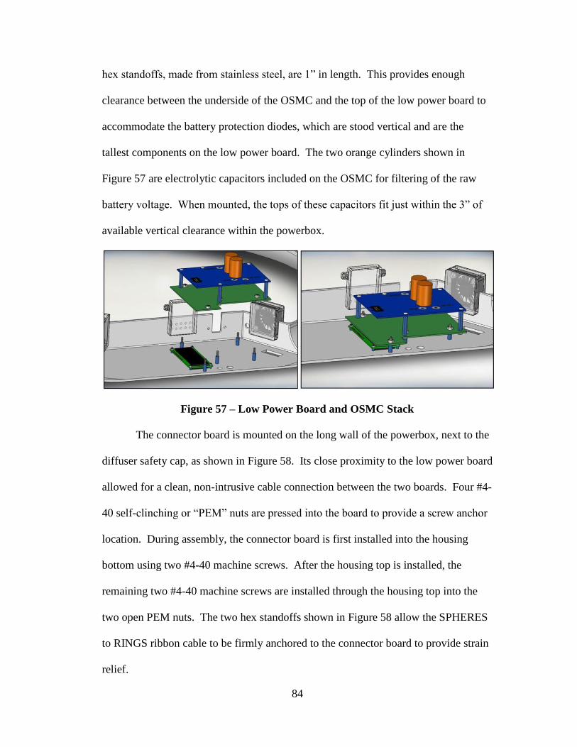
84
hex standoffs, made from stainless steel, are 1” in length. This provides enough
clearance between the underside of the OSMC and the top of the low power board to
accommodate the battery protection diodes, which are stood vertical and are the
tallest components on the low power board. The two orange cylinders shown in
Figure 57 are electrolytic capacitors included on the OSMC for filtering of the raw
battery voltage. When mounted, the tops of these capacitors fit just within the 3” of
available vertical clearance within the powerbox.
Figure 57 – Low Power Board and OSMC Stack
The connector board is mounted on the long wall of the powerbox, next to the
diffuser safety cap, as shown in Figure 58. Its close proximity to the low power board
allowed for a clean, non-intrusive cable connection between the two boards. Four #4-
40 self-clinching or “PEM” nuts are pressed into the board to provide a screw anchor
location. During assembly, the connector board is first installed into the housing
bottom using two #4-40 machine screws. After the housing top is installed, the
remaining two #4-40 machine screws are installed through the housing top into the
two open PEM nuts. The two hex standoffs shown in Figure 58 allow the SPHERES
to RINGS ribbon cable to be firmly anchored to the connector board to provide strain
relief.
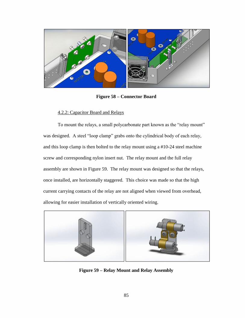
85
Figure 58 – Connector Board
4.2.2: Capacitor Board and Relays
To mount the relays, a small polycarbonate part known as the “relay mount”
was designed. A steel “loop clamp” grabs onto the cylindrical body of each relay,
and this loop clamp is then bolted to the relay mount using a #10-24 steel machine
screw and corresponding nylon insert nut. The relay mount and the full relay
assembly are shown in Figure 59. The relay mount was designed so that the relays,
once installed, are horizontally staggered. This choice was made so that the high
current carrying contacts of the relay are not aligned when viewed from overhead,
allowing for easier installation of vertically oriented wiring.
Figure 59 – Relay Mount and Relay Assembly

86
At this point, the four major remaining components to be fit into the available
powerbox volume were the relay mount, WPT capacitor, and the two EMFF
capacitors. These components were laid out as shown in Figure 60. In Figure 60, the
two larger red boxes are the EMFF capacitors, and the smaller red box is the WPT
capacitor. This arrangement provided sufficient space between the three capacitors
themselves as well as between the capacitors and the side walls of the housing so as
not to impede the cooling airflow. It also resulted in a safe amount of distance
between the components and the resonant coil.
Figure 60 – Capacitor and Relay Mount Setup
The capacitor board was designed to mount directly to the terminals of the
two EMFF caps. This placed the bottom surface of the capacitor board slightly above
the top of the nearby fan box, as well as slightly above the top layer of the resonant
coil. Single wire connections were chosen for the connections from the capacitor
board to each of the four WPT capacitor terminals as well as to the two relays. The
final size and shape of the capacitor board is shown in Figure 61, with the board
shown in transparent yellow for clarity. Various flanges located around the perimeter
of the board were included for the placement of cable headers and single wire
connection terminals.

87
Figure 61 – Capacitor Board Setup
Before installation, the single wire connections to the relays and WPT
capacitor are installed in a compact manner. These connections, as with all the high
current carrying components, were made using American wire gauge (AWG) size 12
wire. Figure 62 shows a picture of the wire connections to the relays and the WPT
capacitor. The heavy gauge of this wire makes it quite stiff, so once the relays and
WPT capacitor were connected, the entire capacitor board unit was very rigid. Figure
63 is an overhead photo of the capacitor board assembly which highlights the
compact nature of the single wire connections, which was imperative to ensure they
did not get too near the resonant coil.

88
Figure 62 – Wire Connections from Capacitor Board to Relays and WPT
Capacitor
Figure 63 – Overhead View of Capacitor Board with Relays and WPT Capacitor
Installed
After the relays and WPT capacitor are wired in to the capacitor board, the
entire assembly is placed into the housing bottom and glued in place using

89
Permabond 820. The adhesive is applied to the bottom surface of the two EMFF
capacitors, the bottom surface of the WPT capacitor, and the bottom surface of the
relay mount. The large available gluing surface area ensures that the capacitor board
assembly stays firmly attached to the housing bottom.
4.2.3: IR Sensor Boards
As discussed earlier, four of the nine IR sensor boards in each RINGS vehicle
are located at joints in the outer fin ring. Since there was not much available volume
here, the IR sensor board was designed to be as compact as possible. By using small
connectors and placing components on both sides of the board, the final dimensions
of the IR boards were reduced to 1.15” x 0.49”.
In addition to the four boards placed on the outer fin ring, four more IR boards
are placed into cavities in the attachment structure struts. As shown in Figure 64, a
polycarbonate cover is placed over the face of the board. Two #4-40 machine screws
thread into two threaded inserts in the strut and hold the cover and IR board in place.
The small groove placed at the bottom edge of the cavity allows for wiring to exit the
cavity and be routed into the housing.
Figure 64 – IR Sensor Board Strut Mounting

90
The ninth and final board is mounted to one of the inner fins, as shown in
Figure 65. This IR sensor board mounts vertically using the same hardware as is used
to mount the outer fin joint IR boards. Whereas the other eight IR boards face away
from the SPHERES satellite of their own vehicle, the inner fin IR board faces directly
towards it. This board was included to guarantee that the IR pulse is detected by the
RINGS vehicle, even if it is only emanating from the SPHERES satellite to which
that RINGS unit is attached.
Figure 65 – Inner Fin IR Sensor Board
4.2.4: Pushbuttons and Switches
The rocker switch is mounted into the housing bottom as shown in Figure 66.
The switch is a “panel-mount” design and contains four small clip features that lock
into the side walls of the housing cutout. Once installed, the clip feature ensures the
switch is securely mounted in place. Also visible in Figure 66 is the switch guard,
which was included to meet NASA safety requirements. The switch guard is a small
nylon piece which is sandwiched between the housing and the rocker switch. Its
purpose is to prevent accidental toggling of the power switch during handling.

91
Figure 66 – Rocker Switch and Switch Guard
One LCD screen select pushbutton and one low battery indicator LED are
each mounted in the housing bottom as shown in Figure 67. They are placed inside
the elbow of the L-shaped cutout in the low power board, allowing for a short wiring
connection to the low power board. Both the pushbutton and the LED are mounted
using hex nuts and lock washers that are included with the components, which
provide back-out prevention. In addition to the pushbutton and LED shown in Figure
67, an additional pushbutton and LED are mounted into a mirrored location in the
housing top.
Figure 67 – LCD Pushbutton and Low Battery Indicator LED Locations
The master clear pushbutton is mounted into the housing bottom on the
oblique powerbox wall nearest to the rocker switch, as shown in Figure 68. Since it is

92
not anticipated that this button will be regularly used, its placement in the small gap
between the support structure strut and the powerbox prevents it from being
accidentally depressed by the operators. Additionally, its close proximity to the low
power board allows for a short wiring connection.
Figure 68 – Master Clear Pushbutton

93
Chapter 5: Simulations
5.1: WPT Modeling
5.1.1: Resonant Inductive Coupling Model
We begin by presenting a model used for investigating the performance of
WPT. The block diagram shown in Figure 69 breaks down the various elements of
the system into their respective transfer functions. Here we are assuming that the
system is composed of two identical coils each having an inductance L and a
resistance R. Some amount of capacitance C is added in series with each of the coils.
Since C is much larger than the self-capacitance of the coils, it will dominate and
hence we can model each coil circuit as a series RLC circuit. An additional
component, the load resistor RL, is placed in series with the secondary coil. The
transfer functions for the primary and secondary coil circuits are shown as Gp and Gs.
Figure 69 – Block Diagram for WPT

94
By Faraday’s law of induction, the magnetic flux generated due to the current
flowing in the primary will induce an EMF in the secondary. The magnitude of this
induced EMF is proportional to the mutual inductance between the coils, which is a
function of coil inductance L and the coupling coefficient κ. The coupling coefficient
κ, which is always between 0 and 1 in value, is a geometric parameter which models
how much of the magnetic flux generated by the primary coil actually penetrates the
secondary coil. Additionally, the current flowing in the secondary will induce an
EMF in the primary, known as the back EMF. The transfer function for mutual
inductance is shown as Gm.
Now we assume that the system is driven by a sinusoidal voltage of frequency
ω0, where ω0 is the resonant frequency of the primary and secondary coil circuits,
given by
(18)
where L is the coil inductance and C is the added capacitance. At resonance, our coil
circuit transfer functions become
(19)
and
(20)
The peak current per volt applied to the primary is then given by

95
(21)
for the primary, and
(22)
for the secondary. Similarly, the power consumed in each coil per volt squared
applied to the primary is given by
(23)
for the primary, and
(24)
for the secondary. The power consumed in the load resistor is given by
(25)
Power transfer efficiency is then given by
(26)
Taking the partial derivative of η with respect to RL gives
(27)
which reveals an expression for the value of RL which maximizes power transfer
efficiency, given by
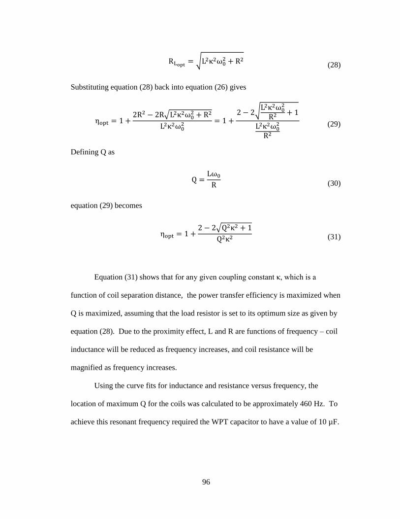
96
(28)
Substituting equation (28) back into equation (26) gives
(29)
Defining Q as
(30)
equation (29) becomes
(31)
Equation (31) shows that for any given coupling constant κ, which is a
function of coil separation distance, the power transfer efficiency is maximized when
Q is maximized, assuming that the load resistor is set to its optimum size as given by
equation (28). Due to the proximity effect, L and R are functions of frequency – coil
inductance will be reduced as frequency increases, and coil resistance will be
magnified as frequency increases.
Using the curve fits for inductance and resistance versus frequency, the
location of maximum Q for the coils was calculated to be approximately 460 Hz. To
achieve this resonant frequency required the WPT capacitor to have a value of 10 µF.

97
5.1.2: Load Resistor Sizing
With the operating frequency for WPT now set at 460 Hz, we proceed with
sizing a load resistor into which power will be transferred. First, however, we need
an approximation for the coupling coefficient κ as a function of coil separation
distance. Assuming that the coils are axially aligned with one another, [9] provides a
means for predicting κ based on separation distance, which was used to calculate a set
of 20 values for κ for separation distances ranging from 0.2 to 2 meters. Then, a
curve fit was applied to these values having the form
(32)
where d is the axial separation distance between the coils and afit and bfit are curve fit
coefficients with values of afit = 0.84 and bfit = -6.25. By using this form of curve fit
equation, the value for agrees with the physical expectations that as d → 0, κ = 1
and as d → ∞, κ = 0. The calculated values and corresponding curve fit are shown in
Figure 70.
Figure 70 – Coupling Coefficient vs. Separation Distance

98
Now that we have an approximation for κ, we can model the predicted power
transfer performance of the system at different separation distances. To do this, we
again assume the primary coil is driven at resonance so that its transfer function is
(33)
where R is the coil’s AC resistance at the WPT frequency of 460 Hz, which is
predicted by the resistance curve fit to be 1.65 Ω. As before, the secondary coil
circuit transfer function is
(34)
where R is 1.65 Ω and RL is the value of the load resistor.
Figure 71 shows the predicted power transferred to the load for three different
load resistor values. Due to the presence of the SPHERES vehicle inside each
RINGS unit, there is a physical limit to how close together the two units can be
positioned. This physical limit is approximately 30 cm and is represented by the
vertical dashed line in Figure 71. For simplicity, each simulation assumes that the
primary is driven with a sinusoidal voltage of 36 volts peak. In reality, the system is
driven by a rectangular wave voltage which decreases in magnitude at higher current
draws due to internal resistance in the batteries, so the predicted levels of transferred
power shown here are slightly overestimated. However, the sinusoidal assumption
still provides valuable insight into the qualitative behavior of the system for different
values of load resistance RL. We see that larger values of load resistance allow for
higher maximum levels of power transfer, but the separation distance at which this
maximum power transfer occurs decreases as the load resistance is increased. Since

99
the RINGS are physically limited to separation distances greater than 30 cm, the 2 Ω
load resistor is most appealing as it allows for the investigation of system
performance both above and below the optimum separation distance for maximum
power transferred.
Figure 71 – Power Transfer Levels for Various Load Resistances
Figure 72 shows the predicted power transfer efficiency η for the same setup
as in Figure 71. As with the total amount of power transferred, we see that the
efficiency of power transfer is higher for larger values of load resistance, but only at
small separation distances. In the region beyond 30 cm, the 2 Ω load resistor
provides the best power transfer efficiency. Based on these results, a load resistor of
2 ohms was chosen.

100
Figure 72 – Power Transfer Efficiency for Various Load Resistances
5.2: Driving Resonant Coil Circuit with Rectangular Wave
As a result of using the H-Bridge drive circuit architecture, the voltage applied
to the coil circuit is an AC rectangular wave whose duty cycle and frequency are
controlled with the onboard microcontroller. Due to the presence of higher frequency
harmonics in the rectangular wave (the frequency of which is not equal to the
resonant frequency of the system), coupled with the fact that the coil’s resistance
increases with frequency, the impedance of the coil circuit varies with the applied
duty cycle. To investigate this phenomenon analytically, we first begin by modeling
the rectangular wave as the sum of two Fourier series expansions for pulse trains.
One of these pulse trains is positive and the other is negative and both have a period
of oscillation T and pulse width τ. The phase difference between the two pulse trains
is 180 degrees. The resulting sum can then be written as
(35)

101
where
(36)
and
(37)
with
(38)
and
(39)
Note that with this notation convention, the duty cycle is given by
(40)
With the input having the form of (35), the steady-state response of the output is
(41)
where the transfer function G is given by
(42)
with

102
(43)
Note that in (42), L and R are functions of frequency as a result of the proximity
effect. We seek to compute the impedance of the circuit, which is given by
(44)
Since the component waveforms of Iss and V are orthogonal, we can rewrite equation
(44) as
(45)
or
(46)
which can be solved computationally to produce the impedance of the circuit at a
given duty cycle. The values of L and R at each harmonic are computed via the curve
fits determined in Section 2.3.
Equation (46) was implemented numerically in a MATLAB script that
calculates the results for the first 300 harmonics. With this large a number of
harmonics, the solution is very well converged to its final value – the 300th
harmonic
only contributes an impedance on the order of e-20. The results for the EMFF
operational mode are shown graphically in Figure 73. Also shown in Figure 73 are

103
experimental results for EMFF mode for duty cycles ranging from 15% to 85% in 5%
increments. To obtain these experimental results, the RMS value of the applied
voltage was measured using a multimeter. The RMS value of the current was
simultaneously measured using an additional multimeter. This setup of measuring
both the applied voltage and the resulting current allowed for calculation of the circuit
impedance. Note that no secondary coil was present when the experimental data was
obtained, as this could have potentially allowed induced EMFs to affect the results.
Figure 73 – Impedance vs. Duty Cycle for EMFF Mode
Additionally, we can determine the resistive component of the impedance by
modifying our transfer function in equation (42). Removing the reactive components,
the new transfer function is
(47)
We can then calculate the reactive component of the impedance by

104
(48)
where Z is obtained from the simulation that uses the transfer function in equation
(42) and R is obtained from the simulation that uses the transfer function in equation
(47). The reactance and resistance values obtained from this analysis are also plotted
in Figure 73. These quantities are useful if one is interested in predicting the power
dissipation in the coil at different duty cycles. The measured impedance values match
up very well to the analytical predictions, both qualitatively and quantitatively. We
also see that the location of minimum impedance in the experimental data, which
occurs at approximately 70% duty cycle, is well predicted by the analytical results.
Figure 74 shows the same results as Figure 73, but for the WPT Transmit
operational mode. The agreement between predicted impedance and measured
impedance is not quite as good as it is in EMFF mode, which is probably due to errors
in the curve fits for R and L. However, we again see a strong qualitative agreement
between the analytical results and the experimental results. One interesting difference
between the EMFF results and the WPT Transmit results is the difference in
reactance between the two operational modes. In EMFF mode, the reactance
contributes a significant amount to the impedance at duty cycles less than 50%.
However, in WPT Transmit mode, the reactance is significantly smaller and hence the
impedance, even at low duty cycles, is predominantly resistive.
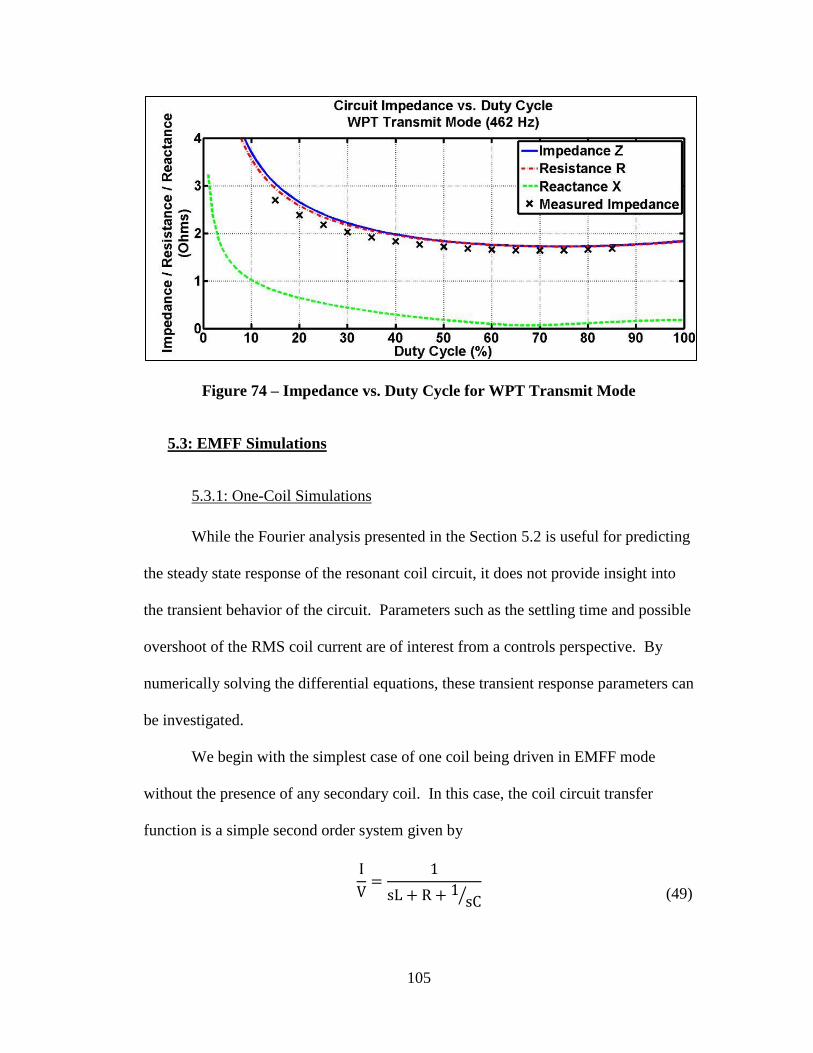
105
Figure 74 – Impedance vs. Duty Cycle for WPT Transmit Mode
5.3: EMFF Simulations
5.3.1: One-Coil Simulations
While the Fourier analysis presented in the Section 5.2 is useful for predicting
the steady state response of the resonant coil circuit, it does not provide insight into
the transient behavior of the circuit. Parameters such as the settling time and possible
overshoot of the RMS coil current are of interest from a controls perspective. By
numerically solving the differential equations, these transient response parameters can
be investigated.
We begin with the simplest case of one coil being driven in EMFF mode
without the presence of any secondary coil. In this case, the coil circuit transfer
function is a simple second order system given by
(49)

106
Using MATLAB’s “lsim” command, the coil current response to an AC
rectangular wave applied voltage was investigated. For simplicity, we ignore the
proximity effect on the higher harmonics by assigning fixed values for the inductance
L and the resistance R. The capacitance and resonant frequency in EMFF mode are
nominally 310 µF and 83 Hz, respectively. From these two numbers, we calculate an
inductance L of 11.9 mH. Choosing a duty cycle of 50%, we then set the resistance R
equal to the experimentally measured circuit impedance at this duty cycle, which is
1.29 Ω. The magnitude of the applied voltage is set to the nominal battery voltage of
36 volts. The results of the simulation are shown in Figure 75. Note that in Figure
75, the RMS current is calculated every half period. We see that the RMS current
settles to 95% of its steady state value in approximately 60 msec, and exhibits no
overshoot. These results are typical for all duty cycles. The settling time of 60 msec
is a good result from a controls perspective, as the commanded current values from
SPHERES are only updated at a frequency of 1 Hz. The lack of overshoot in the
RMS current is also beneficial as it prevents an overcurrent event from occurring
during the transient “ring-up” portion of the coil current response.

107
Figure 75 – One Coil EMFF Transient Simulation
We can also investigate the transient response to a sudden change in the phase
of the applied voltage. This phase change is used in EMFF operations to dictate
whether the two vehicles will attract or repel each other. The results of the phase
change simulation are shown in Figure 76. Here, the simulation was first run for a
length of time which was sufficient for the system to reach steady state conditions
with an input phase angle of 0°. Then, at time t = 0, the input phase angle is set to
180°. All simulation parameters are the same as those used in Figure 75.

108
Figure 76 – One Coil EMFF Phase Change Response
In the steady state conditions seen when t < 0, it is clear that the peak current
occurs in the middle of a driving pulse. With a 50% duty cycle, the middles of the
driving pulses occur at times t1 = (mT+T/8) and t2 = (mT+5T/8), where T is the
period of the applied voltage waveform and m is an integer. This allows us to
determine a “phase settling time,” or the amount of time required for the current to
reach in-phase conditions after the new input is applied at t = 0. Starting at t = 0, we
see that the output does not begin to take on a discernible sinusoidal shape until
approximately halfway through the second period of the applied voltage. The middle
of the second driving pulse of the second period occurs at exactly t1 = (T+5T/8) =
0.01958 seconds. As seen from the graph, however, the peak current occurs at tImax =
0.02000 seconds. This results in a phase error of
(50)
after 20 msec. Applying the same technique to the next location of peak current,
which occurs near the middle of the first driving pulse of the third period, results in a

109
calculated phase error of 1.9% after 26 msec. These results show a phase settling
time, to within 98% of the steady state value, of approximately 26 msec. Though not
visible in Figure 76, the settling time of the magnitude of the RMS current is similar
(~60 msec) to that calculated in the “ring-up” simulation discussed previously.
Another area of interest regarding the rectangular wave input is the
relationship between the applied duty cycle and the resulting coil current. Using the
Fourier analysis presented in Section 5.2, along with the curve fits for inductance and
resistance, an EMFF simulation was carried out to predict the RMS coil current for
duty cycles ranging from 1% to 99% in 1% increments. The results of this
investigation are shown in Figure 77. In addition to the nominal battery voltage of 36
volts, the simulation was also executed with battery voltages of 33 and 30 volts, to
simulate system behavior as the batteries are depleted.
Figure 77 – Coil Currents vs. Duty Cycle in EMFF Mode
We see in Figure 77 that below about 50% duty cycle, a mostly linear
relationship exists between the applied duty cycle and the resulting current in the coil.
The difference in currents between the three different battery voltages is significant,

110
especially at higher duty cycles. This highlights the need for the implementation, on
the PIC, of a duty cycle based current controller, since RINGS does not have the
capability of reading in the battery voltage directly. More discussion on such a
current controller is included in the conclusion chapter.
5.3.2: Two-Coil Simulations
With two coils present, the coil circuit behavior is slightly altered. This is due
to the fact that the same inductive coupling phenomenon used for WPT is also present
in two coil EMFF operations. However, the two coil EMFF setup differs from the
WPT setup in that both coils are actively driven. A block diagram for the two coil
EMFF setup is shown in Figure 78. Here, G1 and G2 represent the transfer functions
for the two coil circuits, and are identical. The two Gm transfer functions represent
the EMF induced in each coil due to the current flowing in the neighboring coil. The
overall effect of these induced EMFs is a reduction in coil currents at close
proximities.

111
Figure 78 – Block Diagram for Two Coil EMFF
The setup shown in Figure 78 is a multiple-input and multiple-output (MIMO)
system. The two system inputs are the voltages applied to each coil circuit and the
two system outputs are the currents in each coil. To analyze the behavior of this
system, a MIMO simulation was created in Simulink. The values for coil inductance,
coil resistance, and the added capacitance are the same as was used in the 1 coil
simulations from Section 5.3.1. Since we are interested in investigating how much
the maximum achievable coil current is affected by the proximity of the two coils, we
set the duty cycle to its maximum value of 99%. As before, the nominal battery
voltage of 36 volts is used for the magnitude of the applied voltage. The coupling
constant κ is computed as a function of axial separation distance using equation (32),
as was done for the WPT simulations. In EMFF mode, the two coils will only ever be
driven either in phase or out of phase with one another – no phase angle other than 0°

112
or 180° will ever be commanded. Consequently, only the two cases of driving in
phase ( Vad1 = Vad2 = 0°) or driving out of phase ( Vad1 = 0°, Vad2 = 180°) are of
interest to us. Running a number of individual simulations with in-phase conditions
and out-of-phase conditions revealed that the current responses in the two coils are
identical to each other for either of these two phase conditions.
A loop was created to investigate the system behavior for axial separation
distances ranging from 1 cm to 1 m in increments of 1 cm. For each separation
distance, the simulation was carried out with a sufficient time span so as to allow the
system to reach steady state conditions, after which the RMS current value of the
final period of oscillation was calculated. The results for the driven-in-phase and
driven-out-of-phase cases are shown in Figure 79. Also shown in Figure 79 is the
minimum possible separation distance of the two vehicles due to the presence of the
SPHERES satellite in the assembly. We see that the two cases are nearly identical,
with the exception of extremely small separation distances. At distances of 1 m and
beyond, the inductive coupling has little effect and our maximum achievable current
is predicted to be 21.5 amps RMS in each coil. At the minimum possible separation
distance of 30 cm, the maximum achievable current is reduced to 18.3 amps, a 15%
reduction from its far-field value. These results indicate that the RINGS vehicles can
still achieve their maximum goal current of 18 amps RMS, even at their minimum
possible separation distance. Since it is unlikely that the RINGS will ever be this
close to each other during typical operations, the inductive coupling in EMFF mode
will have little effect on system performance.

113
Figure 79 – Two Coil EMFF Simulation Results

114
Chapter 6: Conclusions
As discussed in Section 2.3, the proximity effect can cause the frequency of
minimum impedance to be different from the frequency of zero reactance, introducing
a source of error into the test setup. If the tests were repeated, more accurate results
could be obtained by using the Lissajous curve feature on an oscilloscope to measure
the phase angle between the applied voltage and the resulting current. Measuring the
voltage waveform could be achieved by simply connecting a probe across the ends of
the load. To accurately measure the current waveform, one could add a resistor in
series with the load and place a probe across this resistor. The best choice for this
resistor would be a film type composition (due to their low parasitic inductance) in
the mΩ range so as to minimize power dissipation in the resistor. This setup, in
conjunction with the multimeter setup used in the test, would produce more accurate
values of resistance and inductance at different frequencies. Although the assumption
that the frequency of minimum impedance is equal to the frequency of zero reactance
may not apply to higher frequency ranges, they are most likely quite accurate at
frequencies of less than 1 kHz where the proximity effect is not as pronounced. The
lower accuracy of the curve fits at higher frequencies could be the source of error in
the duty cycle versus impedance graphs in Section 5.2, especially in WPT mode.
However, since the calculated frequency of maximum Q (460 Hz) was in the low
frequency range, it is probably very close to the exact frequency of maximum Q.
While the compact coil design was advantageous from a packaging
standpoint, the tight spacing between turns ultimately hindered the WPT capabilities
of RINGS. Even by properly setting the resonant frequency of the system to the point

115
at which the quality factor Q was maximized, only a Q value of approximately 21 was
achieved. By comparison, the one-turn helical design employed in [5] exhibited a
measured Q value in excess of 900. The large discrepancy between the Q values of
the RINGS multi-layer flat spiral design and their one-turn helical design highlights
the massive impact that the proximity effect can have on system performance.
Nonetheless, at present the RINGS system has successfully demonstrated the wireless
transfer of 28 watts at 24% efficiency over a distance of half a meter, which agrees
well with the models presented in Section 5.1.2. The capability for higher levels of
power transfer is anticipated since the primary coil was not driven at its maximum
permissible current level in this test.
Although the resonant coil design is less than ideal for achieving efficient
WPT, it is extremely well suited for EMFF operations. By setting the EMFF
operating frequency to the low value of 83 Hz, the proximity effect does not
significantly increase power dissipation, since the coil resistance at this frequency is
only slightly larger than it is at DC. As a result, the RINGS thermal control system
exhibits good performance even at the high dissipated power levels present when
operating at the maximum design current of 18 amps RMS.
The H-Bridge architecture proved to be an excellent choice for the drive
circuit. Its power dissipation at full current is less than a watt, and it also carries the
intrinsic benefit of allowing the PIC to set any desired frequency and duty cycle for
the applied voltage. A current controller is presently in development at the MIT SSL
and will be implemented on the PIC when complete. The inputs to the controller will
come directly from the onboard Hall Effect current sensors. Once implemented, it

116
will actively adjust the duty cycle to achieve the commanded RMS current, which
will be sent to the RINGS unit from the SPHERES satellite.
A total of four RINGS vehicles were built: two flight units which are currently
(as of April, 2013) in Japan awaiting launch to the ISS, and two engineering
prototype units. The engineering units are currently in use at the MIT SSL where
they are undergoing flat floor testing with the goal of characterizing the dynamics of
the system and implementing EMFF flight controllers. After their construction, the
two flight units spent a week undergoing flat floor testing at the same facility, a
picture of which is shown in Figure 80.
Figure 80 – RINGS Flight Units on the Flat Floor Facility at the MIT SSL
In support of future ISS operations, the two RINGS engineering units are
currently scheduled for testing on a reduced gravity flight campaign in April 2013.
These flights provide 20-30 seconds of microgravity conditions similar to that of the
ISS environment in which the flight units will operate. In addition to the two
engineering units, two SPHERES and a metrology system identical to the one on the
ISS will also be used in the reduced gravity testing. This test setup will allow for a

117
more accurate characterization of the inertia matrix of the vehicles, as well as
gathering of data on the EMFF dynamics at different current levels, separation
distances, and orientations.
118
Bibliography
[1] O. Brown and P. Eremenko, "The Value Proposition for Fractionated Space
Architectures," in AIAA Space 2006 Conference, San Jose, California, 2006.
[2] M. D. Neave, Dynamic and Thermal Control of an Electromagnetic Formation
Flight Testbed (Master's Thesis), Cambridge, MA, 2005.
[3] D. W. Kwon, R. J. Sedwick and A. Sakaguchi, "Micro-Electromagnetic
Formation Flight of Satellite Systems," in AIAA Space 2010 Conference and
Exhibition, Anaheim, CA, 2010.
[4] N. Tesla, "Apparatus for Transmitting Electrical Energy". United States Patent
1,119,732, 18 January 1902.
[5] A. Kurs, A. Karalis, R. Moffatt, J. D. Joannopoulos, P. Fisher and M. Soljacic,
"Wireless Power Transfer via Strongly Coupled Magnetic Resonances," Science,
vol. 317, pp. 83-86, 2007.
[6] A. Karalis, J. D. Joannopoulos and M. Soljacic, "Efficient wireless non-radiative
mid-range energy transfer," Annals of Physics, vol. 323, pp. 34-48, 2007.
[7] P. L. Dowell, "Effects of eddy currents in transformer windings," Proceedings of
the Institution of Electrical Engineers, vol. 113, no. 8, 1966.
[8] V. C. Valchev and A. Van den Bossche, Inductors and Transformers for Power
Electronics, CRC Press, 2005.
[9] F. W. Grover, Inductance Calculations, New York: D. Van Nostrand Company,
1946.


![H20youryou[2] · 2020. 9. 1. · 65 pdf pdf xml xsd jpgis pdf ( ) pdf ( ) txt pdf jmp2.0 pdf xml xsd jpgis pdf ( ) pdf pdf ( ) pdf ( ) txt pdf pdf jmp2.0 jmp2.0 pdf xml xsd](https://img.dokumen.tips/doc/110x75/60af39aebf2201127e590ef7/h20youryou2-2020-9-1-65-pdf-pdf-xml-xsd-jpgis-pdf-pdf-txt-pdf-jmp20.jpg)