Embed Size (px)
Citation preview

AES Hardware-Software Co-Design in WSN
Carlos Tadeo Ortega Otero, Jonathan Tse, and Rajit ManoharComputer Systems Laboratory
Cornell UniversityIthaca, NY, U.S.A.
{cto3,jon,rajit}@csl.cornell.edu
Abstract—Wireless Sensor Networks (WSNs)present a challenging design space for encryptionalgorithms. We evaluate hardware, software, andhybrid implementations, including one of ourown design, of Advanced Encryption Standard(AES) encryption engines in the context of WSNmicrocontrollers. We examine the tradeoffs betweenenergy, throughput, memory footprint, and sensornetwork node lifetime. Our measured results andmodels show that our fully Quasi Delay-Insensitive,asynchronous AES design, combined with a low-powermicrocontroller, offers a 60× increase in throughputat 90× less energy per bit over the commerciallyavailable TI MSP430 AES WSN hardware. Ourhardware AES offers a 30× throughput improvementover its software counterpart, albeit with reducedlifetime. By incorporating power gating and providingdedicated memory resources to the AES engine, hybridimplementations can provide a 6× better throughputand increase the lifetime by 10 % over software.
I. IntroductionWireless Sensor Networks (WSNs) are becoming more
prevalent in a myriad of applications ranging from medicalmonitoring devices to industrial control systems. TypicalWSNs are comprised of many small, low cost nodes ormotes that gather, process, and propagate data abouttheir surrounding environment. Mote deployment lifetimeis often measured in years, so minimizing mote energyconsumption and static power is of great interest.
Aggressive energy reduction at the cost of perfor-mance is a common engineering tradeoff for mote mi-crocontrollers. The Atmel 128L-based MICA2 [6] mote isan example of a relatively high-performance, high-energypoint in the tradeoff space. Smartdust [23] is low-energy(12 pJ per instruction) and low-performance (500 kHz).The Phoenix microcontroller is an extreme example, of-fering 106 kHz at 2.8 pJ per instruction [24]. Recent appli-cation of asynchronous circuit techniques has improved theenergy-performance tradeoff—ULSNAP is a low-energy,fully Quasi Delay-Insensitive (QDI) asynchronous motemicrocontroller design that offers 93 MHz of performanceat only 47 pJ per instruction [21].
High-performance mote microcontrollers like ULSNAPand MICA2 allow more complex computations locally atthe mote, which in turn can reduce the duty cycle ofthe energy-hungry wireless communication systems. How-ever, we must also account for the energy consumptionof encryption, as transmitted information is oftentimessensitive and should be encrypted to preserve confiden-tiality [20]. As of this writing, the Advanced EncryptionStandard (AES) [17] is approved for both non-classifiedand classified information by the US Government and has
has become the industry standard for encryption in appli-cations ranging from SSL to storage media encryption.
Implementing AES in the WSN space is complicatedby the need for a small energy envelope. Typical activitypatterns in the WSN application space are “bursty,” i.e.long quiescent periods followed by a brief, highly-activeperiod. Asynchronous circuits are an excellent fit for theseactivity patterns as they are event-driven, i.e. completelyidle in the absence of data to compute. This intrinsic clock-gating-like behavior of idle asynchronous circuits elimi-nates switching energy during these idle periods withoutsacrificing performance.
As energy consumption is a metric of interest forWSNs, we have developed a model for mote battery life-time in Section II, which accounts for both the energy ofencryption and idle power. To aid the WSN architect, wepresent software, hardware, and hybrid implementationsof AES encryption on WSN microcontrollers, using ourmodel to evaluate the impact to sensor mote lifetime ofeach class of implementation. Our hardware and hybridimplementations are asynchronous to take full advantageof the aforementioned energy benefits. Our WSN moteevaluation platforms are the MSP430 (CC430F6137) [7]and ULSNAP [21], representing the state-of-the-art inWSN platforms providing more than 10 MIPS of perfor-mance in industry and academia, respectively.
II. Mote Lifetime ModelWe adapt the model for sensor node lifetime analysis
used in the work of Jung et al. [8] to include the effectsAES encryption on battery lifetime. The model is a semi-Markov chain formulation of the power state transitionsand satisfies the following properties: ergodicity and Pois-son distribution of event arrivals. An event arrival couldbe the availability of new sensor data, a timer expiringand forcing the mote to execute a pre-planned action, thearrival of a command via the radio, etc. We assume theprocessing, and transmission times are independent andidentically distributed with an arbitrary distribution.
Figure 1 shows our model for the power states of ageneric cryptographic WSN mote: Sensing (S1), Processing(S2) and Transmit or TX (S3). The TX state S3 is anembedded chain of an encryption state, SE , and a datatransmission state, ST . The processing and communicationsteps are optimized for throughput and do not enter alow-energy/low-performance mode when work is available.α represents the probability of data transmission afterprocessing. Figure 2 is a sample encryption power trace.µ1, µ2, and µ3 are the expected averages of sensing time,processing time, and communication time, respectively.The event inter-arrival time is 1/λ. We assume that motes

SensingS1
TXS3
ProcessingS2
SE ST
1
1-α
α1
Fig. 1: Semi-Markov Chain for WSN Mote
S1S1 S1S2 S2 S3
µ1
Inter arrival time: 1/λ
µ2 µ3
Pow
er
t
Fig. 2: Mote Power Profile
rarely receive commands or signals, i.e. they are primarilycollecting, processing, and transmitting sensor data. Ina case where WSN designers expect significant receivetraffic, our model could be extended to include a fourthReceive or RX state. We do not include an RX state here,as we focus primarily on evaluating our AES encryptionengine, as described in Section III.
For both ULSNAP and the MSP430, state S1 is theidle state—i.e. it has the lowest activity factor of all states.In state S1, ULSNAP is effectively clock-gated due to itsQDI circuit implementation [21] and the MSP430 entersa low-power state. The static power consumption of bothsystems is a reasonable proxy for the power consumptionin S1.
Each state Si consumes Ei = tiPi energy, calculatedfrom the consumption Pi and the total time spent in a stateti. Of course, Etotal ≥
∑i Ei. Over a long period, the total
time spent at state Si is given by ti = limt→∞ pit, where piis the proportion of time spent in state Si. Therefore, Ei =pitPi. Let πj be the stationary probability of the Markovchain, which is the frequency of visiting each state overan infinite execution. pij is the probability of transitioningfrom Si to Sj . πj can be interpreted as the proportion oftransitions into Sj .
πj =∑i
πipij ,∑j
πj = 1 (1)
The probabilities pij can be obtained from the Markovchain in Figure 1. The equations can be written in matrixform, where row indices represent source states and columnindices represent end states:
[π1 π2 π3]
[0 1 0
1− α 0 α1 0 0
]= [π1 π2 π3] (2)
The Markov chain model allows us to express pi asfollows, where µi is the mean time spent in Si beforemaking a transition—µ1, µ2, and µ3, respectively:
pi =πiµi∑j πjµj
(3)
Equation (2) and (3) allow us to re-write Etotal andextract t as the mote lifetime:
Etotal ≥ tµ1P1 + µ2P2 + αµ3P3
µ1 + µ2 + αµ3(4)
tlife ≤ Etotal(µ1 + µ2 + αµ3)
µ1P1 + µ2P2 + αµ3P3(5)
Assuming that µ1 ≫ µ2, µ3, we approximate the aver-age sensing time µ1 as the inter-arrival time 1/λ. We alsoexpand the power state S3 into its embedded Markov chainof SE and ST , which means that the mean time spent inS3 can be expressed as the sum of the mean times spentin SE and ST , i.e. µ3 = TE + TT . We can rewrite (5) as:
tlife(λ) ≤Etotal(1 + λ(µ2 + α(TT + TE))
P1 + λ(µ2P2 + α(TTPT + TEPE))(6)
We use (6) in Section IV to compute mote batterylifetime, a key figure of merit for our evaluation.
III. AES ImplementationAES is a 128-bit block cipher with 128-, 192-, or 256-
bit keys (K). Typically, the blocks are logically organizedinto a 4× 4 state matrix of 8-bit elements. A full encryp-tion/decryption step is comprised of several loop iterationsor rounds—10, 12, or 14 rounds for 128-, 192-, and 256-bitkeys, respectively. Each round does four operations on thestate matrix [17]:
1) Add Key (AK)2) Byte Substitution (BS)3) Shift Rows (SR)4) Mix Columns (MC)
Figure 3a shows a simplified dataflow diagram fora complete execution of a 128-bit key AES encryption.The contents of Figure 3a are then wrapped with theappropriate control structures to implement the desiredcipher mode of operation. There are several choices as towhich cipher-block mode to implement. We chose Cipher-Block Chaining (CBC) as it is widely used in the WSNcontext [9] and the simpler Electronic Code Book (ECB)is vulnerable to several attacks [18].
Many WSN motes follow a single-threaded executionmodel to reduce energy consumption. Thus, for a softwareimplementation, the cost of ciphering a single block gov-erns the overall encryption performance for all modes ofoperation. There is also the concern of limited memoryspace for programs on embedded systems. In CBC mode,common hardware optimizations such as pipelining areunattractive in the context of a single encryption becauseof the carried loop dependencies. In practice, some degreeof pipelining is still desired to logically separate the various

Pi
Add Key (AK)
Byte Sub (BS)
Shift Row (SR)
round=10?
Mix Col (MC)
Add Key(AK)
Ci
(a) AES Block Cipher
Pi
Input Gate
+
Add Key (AK)
round=11?
Byte Sub (BS)
Shift Row (SR)
round=10?
Mix Col (MC)
Output
Ci
Port Access
K
Round KeyManager
SRAM11×128bit
(b) CBC ImplementationFig. 3: AES Implementations
stages of encryption, reduce signal fanout, and ease systemdesign.
While WSN motes can occasionally receive encryptedcommands, we assume this is very infrequent and thatthe payload is small. To support decryption, we assumethe existence of a lightweight AES decryption engine insoftware. This assumption allowed us to make a numberof optimizations to our hardware AES encryption engine,as we did not have to support decryption. We note theoptimizations as well as the requirements to support hard-ware decryption below where applicable.
Figure 3b illustrates our encryption engine hardwareimplementation. The unrolled encryption key is stored inan externally user-writeable SRAM. However, only the AKprocess can read the SRAM. SRAM writes and reads arearbitrated by the Port Access process. While our AESengine is implemented at the circuit level as a pipelinedsystem—each box represents a pipeline stage, we treat thesystem as an un-pipelined functional unit when doing asingle encryption. The Input Gate process blocks furtherinputs until it receives a “done” signal from the Outputprocess. Although the pipelining of a single message en-cryption is unattractive due to data dependencies, we cantake advantage of the circuit-level pipelining of our im-plementation by operating on multiple messages. A smallchange to the Input Gate and Output processes allows usto pipeline encryption of multiple messages by interleavingthe plaintext and ciphertext blocks of each message asappropriate.
Our AES implementation (AES-QDI) makes use ofthe Quasi Delay-Insensitive (QDI) family of asynchronouscircuits. We use Martin Synthesis [12], which breaks aparta computation into fine-grained hardware processes thatcommunicate over point-to-point delay insensitive chan-nels. Instead of using a clock and flip-flops for synchro-nization and storage, QDI circuits use channel handshakesfor local, inter-process synchronization and represent dataas tokens traversing these channels. In fact, our AES statematrix is implemented as in-flight data tokens as opposed
en
en
L.dL.v R.v
PCeHB
R.d
R.e
L.e
en
en
en
PDN
PDN
(a) PCeHB Template
PCeHB
f(R′.d)R′.d R.d
R.e
(b) Function BlocksFig. 4: PCeHB Implementations
to being stored in a set of registers. The initial statematrix, i.e. the matrix before the AK step, is input to theencryption engine as a token stream. Once the encryptionis complete, the ciphertext is obtained by collecting theoutput token stream. The overall structure of the statematrix is implemented by proper connectivity and controlin the mux/demux stages between each AES encryptionstep.
QDI hardware processes and the QDI channels them-selves are robust to arbitrary gate delays. As a result, QDIcircuits are intrinsically tolerant to process, temperature,and voltage variations. QDI circuits are also naturallyevent-driven, waiting in a quiescent state with no switchingactivity until a data token arrives. This is the equivalentof perfect clock-gating in a synchronous system—inactiveprocesses consume only leakage current. Since encryptionis typically only active during data transmission in theWSN application space, a QDI implementation effectivelyoffers instantaneous transitions between wake-up/sleepstates with perfect clock-gating.
Our AES-QDI implementation was synthesizedwith PreCharge Half/Full Buffer pipeline templates(PCeHB/PCeFB) [3,11], which have been widely used inmultiple QDI designs [14]. Each PCeHB/PCeFB stageimplements a function of simple enough complexitythat it can fit into a single nMOS Pull-Down Network,as shown in Figure 4a. This compilation style yieldshigh-performance stages with short cycle time and only 2forward transitions.
The signals L.v and R.v are validity signals calculatedby inspecting the input and output data rails L.d andR.d, respectively. As the data rails are encoded with adelay-insensitive protocol, we can obtain validity by in-specting voltage independent of time. We primarily use thehalf-buffer PCeHB templates for computational pipelines.While these templates are high-performance, implement-ing reasonably complex functions usually results in a deeppipeline of PCeHB stages.
As discussed earlier, the carried loop dependenciesinherent in to CBC AES discourage fine-grained pipelin-ing as it increases overall latency. To avoid an over-pipelined design, we combined PCeHB templates withasynchronous function blocks [13], which can be thoughtof as the asynchronous analogue to combinational logic ina clocked pipeline stage. The between-stage handshakingis still handled by the PCeHB handshaking logic, but thecomputation is broken up across the PDN and additional

function blocks placed in series, as seen in Figure 4b.Validity is calculated after the functional blocks have fin-ished computation, with the PDN effectively implementingthe first function in the series chain. This reduces thehandshaking overheads and forward latency per pipelinestage, reducing the overall latency.
To evaluate our design, we performed detailedtransistor-level simulations in SPICE, complete with par-asitics and conservative wire-loads. Our asynchronous de-sign flow does not use a traditional ASIC standard cellflow. We typically generate cells on-demand using CADtools such as cellTK [10], which are then place and routed.Thus, a simulation of a transistor-level SPICE netlist asdescribed represents a simulation of a completed digitaldesign. We compare our implementation with state-of-the-art AES implementations in Section IV-B. We describe theindividual components of the AES system below:
A) Add Key (AK): AK performs a bitwise XOR of eachbyte in the state matrix and the corresponding byte of thecurrent input block. We implemented this block using aPCeHB template with the XOR encoded in the PDN, asthe complexity of an XOR does not warrant additionalasynchronous functional blocks.
B) Byte Substitution (BS): Each byte of the state ma-trix transformed by a non-reversible, non-linear function.In the case of AES, we use a GF (28) Galois Field. Design-ers typically focus their attention on the BS block as ituses almost 75 % of the energy required for an encryption.There are two common ways to implement the BS block:1) Composite Field Transformation (CFT) or 2) Look-UpTable (LUT) [4,15].
CFT is oftentimes implemented as multiplicative in-version followed by an affine transformation. In order tominimize area and pipeline the circuit, the multiplicativeinversion is performed in an equivalent Galois Field, e.g.GF ((24)2). This method usually yields small, pipelinedcircuits with high propagation delays. The composite fieldtransformation can be used for both encryption and de-cryption with minimal changes. CFT-based blocks usuallyhave high throughput, but the long-forward propagationdelay makes CFT unattractive for many AES implemen-tations. However, if overall silicon area is limited, as is thecase in some WSN motes, CFT remains a good option.
A LUT encodes the output values for all possible8-bit input combinations. Possible ways to build thislookup table include using a Product-of-Sums or Sum-of-Products (SOP), or by simply implementing a ROM-basedLUT. More advanced techniques include the use of BinaryDecision Diagrams or Twisted Binary Decision Diagrams(TBDD) [15]. Automated synthesis using commercial toolstypically results in the SOP implementation. A ROM im-plementation typically has lower propagation delays thanthe SOP, but requires a special ROM compiler and doublememory to support both encryption and decryption.
Satoh et al. show that the propagation delay of a BSstage using CFT is 2190 ps in a 130 nm technology. Incontrast, a table lookup takes 700 ps, but at the cost ofa 4.5x increase on the number of transistors [15]. Satoh etal. also propose a TBDD solution that reduces the delayto 430 ps, with a 8x increase in area compared to thecomposite field version.
In our 90 nm technology, we implemented both a CFTand a ROM-based LUT implementation of the BS func-tion. Our CFT implementation has a pipeline depth of 5stages, as shown in Figure 5. The prologue transforms the8-bit vector from a GF (28) to a GF (24)2. The inversionis performed in this Galois Field and then the epiloguetransforms the resulting 2 nibbles to the GF (28). Eachstage of the CFT-based BS is implemented using PCeHBbuffers combined with asynchronous functional blocks, asdescribed earlier and as shown in Figure 4b. We simplifiedthe logic using EXORCISM, a minimization tool for ofExclusive-Sum-Of-Products (ESOP) expressions [25].
encrypt ordecrypt?
Affine−1
δ : GF (28) → GF (24)2)
f : a−1h , a−1
l
δ−1 : GF ((24))2 → GF (28)
encrypt ordecrypt?
Affine
encrypt
decrypt
ah al
a−1h a−1
l
encrypt
decrypt
Fig. 5: Composite Field Transformation Byte Substitution
Our ROM implementation is a 256-row, 8-bit wideNOR-based ROM array. The architecture of our ROMis similar to that described by Nystrom et al. [19]. AROM access has four stages: 1) receive input, 2) decodeinput to address, 3) access ROM at address, 4) transmitoutput. While our ROM implementation has 23 % lessthroughput than CFT, it has 35 % less propagation delay.As the AES CBC algorithm is constrained by loop datadependencies, minimizing delay is a key contributor toperformance. Thus, we used the ROM-based BS for AESdesign, discussed in Table IV.
C) Shift Rows (SR): SR implements a cyclic left shiftfor encryption on each row of the state matrix. The shiftamount for the nth row is n bytes, indexing from zero. Ifsupporting both encryption and decryption is required, i.e.both left and right shifts are necessary, we can compileSR using PCeHB templates to implement the variabledirection shift. Our AES engine is intended for encryptionso we simply implement the shifting with wires, reducingthe delay and energy to the cost of transmission on wires.
D) Mix Columns (MC): MC applies a column-wise 32-bit linear transform to the state matrix. Input columns,denoted a, are treated as a polynomial over GF (28).They are then multiplied by the fixed polynomial c(x) =3x3 + x2 + x + 2 modulo x4 + 1 to obtain the outputcolumn, denoted b. This is equivalent to the matrix vectormultiplication shown in (7).
b0b1b2b3
=
2 3 1 11 2 3 11 1 2 33 1 1 2
a0a1a2a3
(7)

Solving for elements of b requires addition operationsas well as multiplication by factors of 2 and 3. Additionover GF (28) is an XOR and multiplication by 2 is done viashifting followed by an XOR with a constant. Multiplica-tion by 3 can be achieved by a multiplication by two andan XOR addition. Our MC is architecturally similar to [1]and is implemented with PCeHB templates and 2 cascadedfunction blocks, as shown in Figure 6. Implementing MCfor decryption requires multiplication by 9, 11, 13, and 14.These multiplications are typically implemented as lookuptables. Implementing only encryption allows us to avoidthe additional overheads of lookup table ROMs.
⊕ ⊕ ⊕ ⊕
a0 a1 a1 a2 a2 a3 a0 a3
2× 2× 2× 2×⊕ ⊕ ⊕ ⊕
a2 a3 a0 a1
⊕ ⊕ ⊕ ⊕
b0 b1 b2 b3
Fig. 6: Mix Columns
IV. AES EvaluationIn our study, we benchmarked and analyzed software,
hardware, and hybrid AES implementations for two micro-controllers: the commercially available TI MSP430, versionCC430 [7], and ULSNAP [21]. A similar analysis can be ap-plied to any other microcontroller platform. The MSP430provides a completely in-silicon solution for AES, whichserves as a data point for commercial WSN AES hardware.ULSNAP is a microcontroller design from academia tar-geted for the WSN space. ULSNAP employs a number ofadvanced techniques at both the circuit and microarchitec-tural levels to improve energy efficiency while maintainingperformance [21]. The MSP430 CPU implements a 16-bit,single-pipeline Von Neumann architecture with a modernRISC ISA. ULSNAP is also 16-bit and has a MIPS-likeRISC ISA, but implements a Harvard architecture. WhileULSNAP does not have explicit active power modes, bychanging the operating voltage the user can choose high-performance and low-power characteristics.
ULSNAP makes use of the QDI family of asynchronouscircuits [21]. That makes ULSNAP robust to systemic andrandom variations from manufacturing, temperature andvoltage. The compilation of QDI processes implements theequivalent of the perfect clock-gated synchronous circuits–inactive processes consume only leakage current. Withrespect to our model described in Section II, we assumeregularly spaced sensor events, each of which has proba-bility α of causing the transmission of a single encryptedpacket after being processed.
We have access to a number of packaged, functional90 nm ULSNAP dies. All ULSNAP software implemen-tation results are measured data from actual on-siliconexecutions of compiled code. The TI CC430 is commer-cially available, so all results which do not involve our
AES implementations are from measurements of a physicalMSP430 device. Results for our AES implementation arefrom SPICE simulations of a completed, sized, transistor-level design netlist annotated with conservative wire andother parasitic capacitances.
As described in Section III, our transistor-level netlistis a complete design, ready for place and route and sub-sequent fabrication. Our SPICE simulation flow is well-characterized against silicon chips and often returns moreconservative numbers than simulations of extracted layoutand actual die measurements. Results for the hybrid con-figurations below are a combination of SPICE simulationsand measurements from silicon as appropriate.
The total size of a transmitted packet packet is 133 Bwith a payload of 127 B. This payload is the maximumallowable for a Zigbee packet as defined by the IEEE802.15.4 standard. The transmission time of a packet,TT , is set by the transmission rate. We assume that ourmotes use the TI-CC1101 transceiver, which offers 500kbpsof bandwidth at 55 mW [26]. Using this transceiver isa natural fit for the MSP430, and we assume ULSNAPcan be paired with the CC1101 or an equivalent radio.Transmitting a 133 B packet takes TT = 2.12 ms.
We assume the average processing time for each eventto be µ2 = 1.1 ms, which is the average completion timefor the statistical benchmark set from the SenseBenchsuite [16] running on ULSNAP [21]. µ1 and TE are de-pendent on the event inter-arrival time and AES imple-mentation, respectively. Note that encrypting the 127 Bpayload takes 8 full encryptions, which we have accountedfor in our evaluation below.
A. Software-Only ApproachIn order to maximize energy efficiency, programmers
can leverage different processor power modes. The MSP430implements four active power modes, which offer a tradeoffbetween power and performance, and five sleep modes,which offer a tradeoff between static power and wakeup time. In high performance (HP) active mode, theMSP430 core consumes 4.5 mA at 2.4 V, which translatesto about 54 nJ per operation. For the MSP430, an opera-tion equates to a complete instruction execution. Whenrunning in low-energy (LE) active mode, the MSP430consumes 160 µA/MHz with a minimum voltage of 1.8 V.The maximum frequency in low-energy mode is 1 MHz foran energy per instruction of 28 pJ.
ULSNAP does not have discrete power modes butrather scales performance continuously with operatingvoltage due to its QDI circuit implementation [21] andenters sleep mode automatically once all events have beenprocessed. At 1.2 V or HP mode, ULSNAP runs at 93 MHzand draws 3.45 mA—47 pJ per instruction. At 0.95 V orLE mode, ULSNAP offers 47 MHz at 1.3 mA, or 29 pJ perinstruction on average [21].
Table I shows the power and performance for fourdifferent software implementations of AES running at thehigh and low power modes of our test microprocessors. TI-C and ULSNAP-C are evaluations of the same AES librarywritten in C compiled for the MSP430 and ULSNAP,respectively. TI-MSP430 is a Texas Instruments soft-ware implementation of AES optimized for the MSP430.
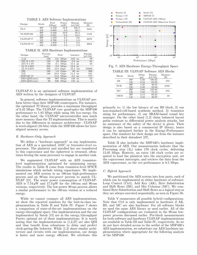
TABLE I: AES Software ImplementationsPerf. Power Energy MemoryDesign Mode [Mbps] [mW] [nJ/bit] [B]
HP 0.102 10.8 105.4TI-C LE 0.005 0.2 56.1 3441HP 0.420 10.8 25.3TI-MSP430 LE 0.021 0.2 13.5 1184HP 1.550 4.1 2.6ULSNAP-C LE 0.786 1.2 1.5 2670HP 1.850 4.1 2.2ULSNAP-O LE 0.935 1.2 1.3 2664
TABLE II: AES Hardware ImplementationsProcess EnergyDesign [nm] Perf. Latency [pJ/bit]
[1,2] 130 141 Mbps 910 ns 79[27] @ 1.5V 130 23 Mbps 5.6 µs 81[27] @ 1.0V 130 8.1 Mbps 15.4 µs 43[4] @ 3.30V 350 9.9 Mbps 12.9 µs –[4] @ 0.65V 350 12.8 kbps 10.3 ms 55000[28] 180 1.6 Gbps 80 ns 300[15] 130 10.0 Gbps 11.3 ns 191
MSP430 [7] – 15.0 Mbps 8.5 µs 717AES-QDI(ours) 180 907 Mbps 138 ns 34AES-QDI(ours) 90 948 Mbps 135 ns 8
ULSNAP-O is an optimized software implementation ofAES written by the designers of ULSNAP.
In general, software implementations on ULSNAP per-form better than their MSP430 counterparts. For instance,the optimized TI library provides a maximum throughputof 0.42 Mbps. The ULSNAP core quadruples the MSP430performance to 1.85 Mbps while using 10x less energy. Onthe other hand, the ULSNAP microcontroller uses muchmore memory than the TI implementations. This is mostlydue to the differences in memory architecture—ULSNAPis word-aligned (16-bits) while the MSP430 allows for byte-aligned memory access.
B. Hardware-Only ApproachWe define a “hardware approach” as any implementa-
tion of AES as a specialized ASIC or transistor-level co-processor. The plaintext and unrolled key are transferredto this coprocessor and the ciphertext is returned, often-times freeing the main processor to engage in another task.
We augmented ULSNAP with an AES transistor-level implementation optimized for minimizing energy.The results in Table II come from transistor-level SPICEsimulations which include wiring capacitance. We imple-mented our AES system in an 180 nm high-performanceprocess and an 90 nm low-power process to match UL-SNAP [21]. The static power consumption of ULSNAP-AES is 7.54 µW and 17.3 µW for the 180 nm and 90 nmversions, respectively. The low-power 90 nm process allowsa similar performance to the 180 nm version at a reducedenergy.
While we cannot compare all AES implementations,we show the reported numbers for the best-in-class im-plementations in Table II and Table IV. Figure 7 showsa comparison of state-of-the-art implementations on theenergy-throughput space. Our implementation and the oneimplemented by Satoh [15] are in the energy/throughputPareto optimal set of these implementations. It is worthnoting that the implementations in [1,2,27] are also QDIand thus benefit from robustness to delay and perfectclock-gating-like behavior. While [1,2] share similar archi-tecture and circuits with our implementation, our designis faster and more energy efficient. We attribute this
101 102 103 104
Performance [Mbps]
100
101
102
103
Ener
gy[p
J]
Bouesse [2]Tiempo 1.5VTiempo 1.0VVerbauwhede [28]
Satoh [15]MSP430 [7]ULSNAP-AES (180nm)ULSNAP-AES (90nm-Low Power)
Fig. 7: AES Hardware Energy-Throughput SpaceTABLE III: ULSNAP Software AES Blocks
Delay Energy MemoryBlock Mode [µs] [pJ/bit] [B]HP 3.30 106.82AK LE 6.54 63.05 452HP 1.25 40.55SUB LE 2.48 23.94 1058HP 3.88 125.62MC LE 7.68 74.15 552HP 2.14 69.24MEM LE 4.24 40.87 40
primarily to: 1) the low latency of our BS block, 2) ournon-standard-cell-based synthesis method, 3) transistorsizing for performance, 4) our SRAM-based round keymanager. On the other hand [1,2] claim balanced layoutpaths resistant to differential power analysis attacks, butno assurance of the safety of the device is given. Theirdesign is also based on a commercial IP library, henceit can be optimized further in the Energy-Performancespace. Our numbers for their design are from the instancedescribed in their datasheet [27].
Table II also includes the MSP430’s hardware imple-mentation of AES. Our measurements indicate that theProcessing step (S2) takes 170 clock cycles, delivering15.05 Mbps. However, an extra 140 clock cycles are re-quired to load the plaintext into the encryption unit, setthe coprocessor interrupts, and retrieve the data from theAES coprocessor, so the net performance is 8.5 Mbps.
C. Hybrid ApproachWe partitioned the AES system into four parts, each of
which can be implemented in either hardware of software:Loop Control (Ctrl), Add Key (AK), Byte Substitutionand Shift Rows (BS), and Mix Columns (MC). We com-bined Byte Substitution and Shift Rows as a logical step asthey are always executed sequentially, as seen in Figure 3b.
Table V enumerates all possible hybrid configurations.Note that Ctrl is only implemented in hardware if AK,BS, and MC are also hardware. For all software blockswe used the same AES library as used earlier. All of theULSNAP configurations are evaluated in the 90 nm low-power process discussed earlier. Per-block measurementsfor both software and hardware ULSNAP implementationsare available in Table III and Table IV, respectively. As wedo not have detailed access to the netlist of the MSP430’sAES implementation, we substitute our AES hardware im-plementation where appropriate for the following analysisof the MSP430.

TABLE IV: Hardware AES-QDI BlocksPerf. Energy Txr Delay PstaticBlock [MHz] [pJ/bit] [×1000] [ns] [µW]
AK 370 0.140 28.65 0.21 0.47MC 281 0.136 14.57 0.57 0.80BS - ROM 155 0.351 7.45 3.54 0.84BS - CFT 192 0.750 5.49 4.83 †0.29Ctrl/Key SRAM 107.7 11.30
†: Encryption and Decryption
We augment our model from Section II by defining Thybas the block encryption time of our hybrid system. Tload,as seen in (8), is the time to load data into the accelerator,which we assume is similar to the cost of accessing memory.TAK , TBS , and TMC are the execution times for the AK,BS, and MC units, respectively. The coefficients belowrepresent the total number of executions of each unit fora complete encryption, including the load time Tload:
Thyb = 10Tload + 11TAK + 10TBS + 9TMC (8)Thw = Tload + TE (9)
THSH = 10Tload + Thyb (10)
The differences between the hybrid execution time in(8) and the hardware execution time in (9) are as follows:A full hardware implementation needs a single access tothe encryption data whereas a hybrid implementationmust effectively access ten times by transferring databetween the hardware and software blocks. TE accountsfor the double encryption necessary to send a 29 B packet.If AK and MC are implemented in hardware but BSis implemented in software, we incur an additional tenmemory accesses as we need to retrieve the data twice, asshown in (10). We refer to this combination as “hardware-software-hardware (HSH).”
Table V lists our estimated performance and lifetimenumbers for hybrid implementations of AES on ULSNAPand the MSP430, using our hybrid AES implementationsalongside both processors. The throughput was calculatedby adding the delay of blocks from Table III and Ta-ble IV as appropriate. As a validation of our estimates,the software only approach in Table V, configuration 8,matches the measured result in Table I (ULSNAP-C) towithin 1 %. Similarly, the software only approach of theMSP430 matches the (TI-C) result from Table I. The TI-C software implementation fuses the AK and BS steps, sowe did not evaluate hybrid combinations of AK and BS onthe MSP430.
tlife in Table V is an estimate of mote battery life fromour model, assuming an inter-arrival rate of 1/λ = 1 min.The static power consumed in state S1 accounts for thatof the microcontroller as well as that of any hardware-implemented blocks, as estimated in Table IV.
Our full-hardware implementation is roughly 180ktransistors, effectively 30 % of the reported 592k transis-tors comprising ULSNAP [21]. We assume that the BScomputation is parallelized and requires four S-box. TheCtrl unit is roughly double the size of the sum total of allindividual blocks. Table V shows an all-hardware imple-mentation offers the best throughput. Moving to software-based control of the hardware results in a 10x penaltyto throughput. However, a full-hardware implementationalso has the lowest mote lifetime as the static powerconsumption from the additional transistors dominatesdue to the long idle time.
10−3 10−2 10−1 100 101 102 103
Inter-arrival Time: 1/λ [s]
0100200300400500600
Nod
eL
ifet
ime
[day
s] 5min1s
Full HWH,H,HH,S,HS,S,S
�∧◦?
(a) Lifetime
10−3 10−2 10−1 100 101 102 103
Inter-arrival Time: 1/λ [s]
0100200300400500600
Nod
eL
ifet
ime
[day
s] 5min1s
Full HWH,H,HH,S,HS,S,S
�∧◦?
(b) Lifetime with Power GatingFig. 8: ULSNAP Lifetime
10−3 10−2 10−1 100 101 102 103
Inter-arrival Time: 1/λ [s]
0100200300400500600
Nod
eL
ifet
ime
[day
s] 5min1s
Full HW�S,S,S?H,S,H◦H,H,H∧
Fig. 9: ULSNAP Lifetime with Memory Overheads
Figure 8a shows the lifetime of various hybrid AESconfigurations alongside ULSNAP as function of the eventinter-arrival time (1/λ). For 1/λ < 4 s, the hybrid schemesoffer better performance than a software-only implemen-tation with little or no impact in the lifetime of the mote.In contrast, for sparse events tlife is governed by the staticpower. For inter-arrival times greater than 5 minutes,Figure 8a shows a gap in excess of 3x between the hybridand software counterparts.
The simple addition of power-gating cut-off transistorsin QDI circuits reduces idle power consumption. We sizedthe sleep transistors to reduce static power consumptionby an average of 80 % with an average of 20 % performancedegradation [22]. This is particularly beneficial for thefull-hardware configuration. Incorporating these estimatedpower gating savings provides 50- to 100-percent improve-ment in mote lifetime for sparse arrival times, as seen inFigure 8b.
Figure 8a and Figure 8b assume that the softwareportions of the hybrid AES implementations share memorywith the host microprocessor. Adding dedicated memoryfor the AES unit to alleviate memory contention withthe host processor results in Figure 9, assuming 120 pA ofleakage current per SRAM bitcell [5]. In this scenario, thehybrid modes actually offer the best lifetime. The staticpower of the dedicated memory for the software-only modeincreases to the point that the software-only lifetime is only
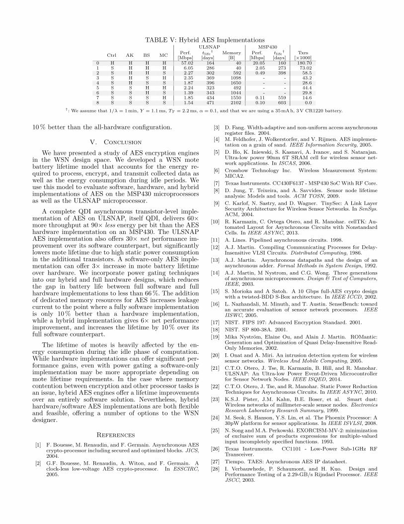
TABLE V: Hybrid AES ImplementationsULSNAP MSP430
Perf. tlife† Memory Perf. tlife
† TxrsCtrl AK BS MC [Mbps] [days] [B] [Mbps] [days] [×1000]0 H H H H 57.02 164 40 20.05 160 180.701 S H H H 6.05 286 40 2.05 273 73.022 S H H S 2.27 302 592 0.49 398 58.53 S H S H 2.35 369 1098 - - 43.24 S H S S 1.87 396 1650 - - 28.65 S S H H 2.24 323 492 - - 44.46 S S H S 1.39 343 1044 - - 29.87 S S S H 1.85 434 1550 0.11 559 14.68 S S S S 1.54 471 2102 0.10 603 0.0
†: We assume that 1/λ = 1 min, Y = 1.1 ms, TT = 2.2 ms, α = 0.1, and that we are using a 35 mA h, 3 V CR1220 battery.
10 % better than the all-hardware configuration.
V. ConclusionWe have presented a study of AES encryption engines
in the WSN design space. We developed a WSN motebattery lifetime model that accounts for the energy re-quired to process, encrypt, and transmit collected data aswell as the energy consumption during idle periods. Weuse this model to evaluate software, hardware, and hybridimplementations of AES on the MSP430 microprocessorsas well as the ULSNAP microprocessor.
A complete QDI asynchronous transistor-level imple-mentation of AES on ULSNAP, itself QDI, delivers 60×more throughput at 90× less energy per bit than the AEShardware implementation on an MSP430. The ULSNAPAES implementation also offers 30× net performance im-provement over its software counterpart, but significantlylowers mote lifetime due to high static power consumptionin the additional transistors. A software-only AES imple-mentation can offer 3× increase in mote battery lifetimeover hardware. We incorporate power gating techniquesinto our hybrid and full hardware designs, which reducesthe gap in battery life between full software and fullhardware implementations to less than 66 %. The additionof dedicated memory resources for AES increases leakagecurrent to the point where a fully software implementationis only 10 % better than a hardware implementation,while a hybrid implementation gives 6× net performanceimprovement, and increases the lifetime by 10 % over itsfull software counterpart.
The lifetime of motes is heavily affected by the en-ergy consumption during the idle phase of computation.While hardware implementations can offer significant per-formance gains, even with power gating a software-onlyimplementation may be more appropriate depending onmote lifetime requirements. In the case where memorycontention between encryption and other processor tasks isan issue, hybrid AES engines offer a lifetime improvementsover an entirely software solution. Nevertheless, hybridhardware/software AES implementations are both flexibleand feasible, offering a number of options to the WSNdesigner.
References[1] F. Bouesse, M. Renaudin, and F. Germain. Asynchronous AES
crypto-processor including secured and optimized blocks. JICS,2004.
[2] G.F. Bouesse, M. Renaudin, A. Witon, and F. Germain. Aclock-less low-voltage AES crypto-processor. In ESSCIRC,2005.
[3] D. Fang. Width-adaptive and non-uniform access asynchronousregister files. 2004.
[4] M. Feldhofer, J. Wolkerstorfer, and V. Rijmen. AES implemen-tation on a grain of sand. IEEE Information Security, 2005.
[5] D. Ho, K. Iniewski, S. Kasnavi, A. Ivanov, and S. Natarajan.Ultra-low power 90nm 6T SRAM cell for wireless sensor net-work applications. In ISCAS, 2006.
[6] Crossbow Technology Inc. Wireless Measurement System:MICA2.
[7] Texas Instruments. CC430F6137 - MSP430 SoC With RF Core.[8] D. Jung, T. Teixeira, and A. Savvides. Sensor node lifetime
analysis: Models and tools. ACM TOSN, 2009.[9] C. Karlof, N. Sastry, and D. Wagner. TinySec: A Link Layer
Security Architecture for Wireless Sensor Networks. In SenSys.ACM, 2004.
[10] R. Karmazin, C. Ortega Otero, and R. Manohar. cellTK: Au-tomated Layout for Asynchronous Circuits with NonstandardCells. In IEEE ASYNC, 2013.
[11] A. Lines. Pipelined asynchronous circuits. 1998.[12] A.J. Martin. Compiling Communicating Processes for Delay-
Insensitive VLSI Circuits. Distributed Computing, 1986.[13] A.J. Martin. Asynchronous datapaths and the design of an
asynchronous adder. Formal Methods in System Design, 1992.[14] A.J. Martin, M Nystrom, and C.G. Wong. Three generations
of asynchronous microprocessors. Design & Test of Computers,IEEE, 2003.
[15] S. Morioka and A Satoh. A 10 Gbps full-AES crypto designwith a twisted-BDD S-Box architecture. In IEEE ICCD, 2002.
[16] L. Nazhandali, M. Minuth, and T. Austin. SenseBench: towardan accurate evaluation of sensor network processors. IEEEIISWC, 2005.
[17] NIST. FIPS 197: Advanced Encryption Standard. 2001.[18] NIST. SP 800-38A. 2001.[19] Mika Nyström, Elaine Ou, and Alain J. Martin. ROMantic:
Generation and Optimization of Quasi Delay-Insensitive Read-Only Memories, 2002.
[20] I. Onat and A. Miri. An intrusion detection system for wirelesssensor networks. Wireless And Mobile Computing, 2005.
[21] C.T.O. Otero, J. Tse, R. Karmazin, B. Hill, and R. Manohar.ULSNAP: An Ultra-low Power Event-Driven Microcontrollerfor Sensor Network Nodes. IEEE ISQED, 2014.
[22] C.T.O. Otero, J. Tse, and R. Manohar. Static Power ReductionTechniques for Asynchronous Circuits. In IEEE ASYNC, 2010.
[23] K.S.J. Pister, J.M. Kahn, B.E. Boser, et al. Smart dust:Wireless networks of millimeter-scale sensor nodes. ElectronicsResearch Laboratory Research Summary, 1999.
[24] M. Seok, S. Hanson, Y.S. Lin, et al. The Phoenix Processor: A30pW platform for sensor applications. In IEEE ISVLSI, 2008.
[25] N. Song and M.A. Perkowski. EXORCISM-MV-2: minimizationof exclusive sum of products expressions for multiple-valuedinput incompletely specified functions. 1993.
[26] Texas Instruments. CC1101 - Low-Power Sub-1GHz RFTransceiver.
[27] Tiempo. TAES: Asynchronous AES IP datasheet.[28] I. Verbauwhede, P. Schaumont, and H. Kuo. Design and
Performance Testing of a 2.29-GB/s Rijndael Processor. IEEEJSCC, 2003.