Embed Size (px)
Citation preview
IntroductionTraditional two dimensional design tools often fall short when it comes to studying the structure and routability of the advanced packages required for today’s complex designs.
Virtual prototyping of the optimal floorplan is beneficial, along with the ability to access verification tools as early as possible in the process. Tools that support 3D system-level design, which also seamlessly connect with verification tools, can significantly improve the package design process.
A more intelligent approach to package design is one in which the chip, package and board can be designed simultaneously. Zuken’s Design Force native 3D chip, package and board co-design environment enables design and optimization of the interfaces between all three domains throughout the design flow.
Design Force offers an intuitive, integrated environment for designing single and multi-die packages for wire-bond, flip-chip, and high density advanced packaging. Designers can start designs with early prototype input of chip and package data from the library, reuse data from IC layout tools, and take advantage of parametric wizards to streamline the creation of the system. Design Force includes support of 2D- and 3D-based design and manufacturing rules to ensure the package is designed right-the-first-time.
With its native 3D platform, designers can easily implement and manage dense interconnects for wire bond or flip chip packages, and incorporate embedded component technology for advanced packaging and module design.
™ Advanced PackagingDesign Force
zuken.com/CR-8000
Top features and benefi ts
SiP (system-in-package)
• Unifi ed environment to handle packaging technologies, including chip scale packaging (CSP), multi-chip modules (MCMs), and system-in-package (SiP).
• Parametric wizards for chip and package structures reduce time and eff ort for implementing complex package designs.
• Automatic ball assignment with the ability to optimize complex routing solutions.
• Conduct feasibility studies and shorten design implementation with advanced fan-out/fan-in and autorouting features to optimize package layer count.
• 2.5/3D stacking structures handled in any confi guration: stacked, adjacent, interposers, with wire bond and fl ip chip packages.
• Native 3D environment enables true rules-driven approach to ensure designs are implemented and verifi ed accurately.
• Hierarchical database allows users to conduct co-design with ICs and PCBs in one environment to realize the latest technologies, such as 2.5/3D IC design.
Challenges faced by package designers using traditional tools include: • Using many disparate tools to design
the chip, package and board• Manual exchange of ASCII fi les to
communicate description and changes• Limited ability to share constraints
across the system• Lack of common environment to
manage complete system-level design.
Why co-designChip-package-board co-design is a methodology for designing and optimizing the layout of chip IOs, package and board in single environment. Traditionally each layout is managed by different groups within an organization. Design Force enables designers to work in a co-design environment in order to optimize the layout of their design across all three domains: chip, package and board.
The Design Force co-design flow takes into consideration redistribution layer (RDL) routing, package escape, routability and parasitics, and enables simultaneous tradeoffs between chip and package design. It can construct the package design hierarchically with the chip and PCB, to offer designers improved system performance at the lowest cost through I/O optimization in one environment.
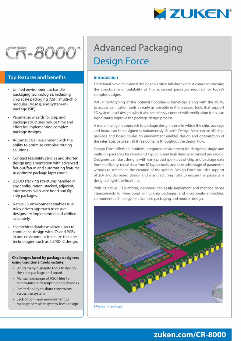
The impact of flip-chipsFlip-chip methodology is commonly used for high I/O count designs. This methodology greatly reduces inductance, allows high-speed signals, and possesses better heat conductivity properties. An RDL is used to connect I/O pads to solder bumps. RDL congestion issues arise when a single layer in spite of manual routing is not enough to complete the routing for a sizable design due to sub-optimal I/O placement. Hence, in multiple die packaged systems for flip-chips, RDL routing is the key to packaging tradeoffs. To achieve a high performance and low cost chip-package-board system, early feasibility analysis is a must to allow physical constraints to be coupled to electrical requirements. The physical constraints are used to minimize total wire-length of the RDL routes, whereas the electrical requirements are used to ensure accurate signal-power ratio, low power consumption, reduced inductance and lower thermal effects. The impact of electrical performance needs to be understood and addressed in the prototype stage well before the final implementation.
Ease-of-useDesign Force includes an array of utilities and wizards to accurately define wire-bond profiles, bond pad placement, multi-die or bond-pad connections, managing the stacking of ICs with online design and manufacturing rule checks. Designers can leverage the many interactive and automatic routing tools to reduce effort conducting fan-in/fan-out routing, automatic ball assignments on the package, and routing of the complete package.
Utilizing the latest in computing technologyDesign Force takes advantage of the latest hardware and software platforms with a native 64-bit architecture using multi-core, multi-threading processes, with support of OpenGL and DirectX graphics for the best possible performance.
Design Force is engineered and architected to comply with the most current network applications, including standalone client, data server, application server and cloud computing.
Interface to best-in-class CAE tools Design Force supports integrations to best-in-class tools from partners such as ANSYS, AWR, Agilent and Synopsys for RF, Full Wave FD/TD, power integrity, and thermal extraction and analysis. This allows designers to address key issues early in the design process. Design Force also contains native EMI, signal and power integrity analysis for eliminating design errors.
Additional features of Design Force Advanced Packaging
• Co-design system-in-package (SiP), package-on-package (PoP), package-in-package (PiP), and through-silicon-via (TSV) with bidirectional support for exchanging SoC information using OpenAccess and Library Exchange Format / Design Exchange Format (LEF/DEF) formats.
• IC co-design structures imported with LEF/DEF are easily placed and manipulated using intuitive and well-documented scripting environments.
• User-configurable menu buttons and menu bar enable a highly customizable UI allowing reuse for executing common functions and routines.
• Package feasibility router predicts the likelihood of routing success for multi-layer package designs at the bump/ball pattern definition stage.
• Design any packaging technology:• Flip-chip• Wire-bond• System-in-Package, multi-chip module.
• Hierarchical database enables:• Package-on-Package• Package-in-Package• Interposer design• Support for TSVs• RDL and die bump design.
All trademarks mentioned are the property of their respective owners. Copyright © Zuken. 150826 zuken.com/CR-8000
Flip chip with redistribution layers in native 3D