Embed Size (px)
Citation preview

MC44722A/3A Rev 0.05 07/15/98No.
This document contains information on a new product. Specifications and information herein are subject to change without notice.
1
Advanced Information
Advanced Digital Video EncoderY/Cb/Cr Output SupportHCMOS Technology
MC44722AMC44723A
The MC44722A and MC44723A are advanced Digital Video Encoders (DVE). They convert ITU-601/656 standard 4:2:2 Bit-Paralellel data into analog composite video, S-Video or analog component signals Y/Cb/Cr in PAL and NTSC formats. They accept the multiplexed two 8-bit or 16-bit ((CB,Y,CR)Y) signals from digital sources such as MPEG decoders and can act as a sync generator master or as a sync slave. All video processing is done digitally and requires no external adjustment.
Specifically designed for digital satellite, digital cable decoders, multimedia terminals and DVD players.
• World Wide Operation (PAL-BDGHI, PAL-N,PAL-M, NTSC-M)• SMPTE 170M / ITU - R 624 composite video output • Programmable Color Sub-carrier Frequencies• Analog standard timing for Horizontal, Vertical, Frame and Composite Sync Outputs• Sync Extraction From Digital Input Data (SAV, EAV)• Sync Polarity and Horizontal / Vertical Phase Control• Master or Slave Sync (H/Vsync, H/Fsync, ITU-R656 Slave) Operation• Interlaced or Non-Interlaced Support• 625/50 or 525/60 ITU-601/656 two 8-bit or 16-bit ((CB,Y,CR)Y) Digital Input• Luma 2X / Chroma 4X Output interpolating Filter• Dual Digital A / B selectable inputs• External VBI Information Data Input (Teletext Information Data)• Selectable One set of Signal within (CVBS/Y/C) or (Y/Cb/Cr)• Selectable Analog Component Output ( Beta Cam or MII Component Interface Level )• Three Analog Outputs Through 10-bit DACs• Easily programmed via Serial Bus ( I2C or 4-Wired SPI Bus)• 2 Hardware selectable I2C Chip Addresses • Closed-Caption, CGMS and WSS Information data Insertion• MACROVISION ver. 7.01 Anti-Copy Signal Insertion(MC44722A Only)• On Chip Color - bar Generator• 5V Tolerante Input • +3.3V Power Supply or +3.3V(Digital)/+5V(Analog) Power Supply• Pin Compatible with MC44722/3
The MC44722A device is protected by U.S. patent number 4,631,603,4,577,216 and 4,819,098 and other intellectual property rights. The use of Macrovision's copy protection technology in the device must be authorized by Macrovision and is intended for home and other limited pay-per-view uses only, unless otherwise authorized in writing by Macrovision. Reverse engineering or disassembly is prohibited.
FT SUFFIX 48 QFP
(0.8mm Pitch)
VFU SUFFIX 48 VQFP
(0.5mm Pitch)
Fre
esc
ale
S
em
ico
nd
uc
tor,
I
For More Information On This Product, Go to: www.freescale.com
nc
...

MC44722A/3A Rev 0.05 07/15/98No.
This document contains information on a new product. Specifications and information herein are subject to change without notice.
[Pin Assignment]
2
CVBS / Cb Hsync
C/Fsync/VBI
Vmute
DVIA3
DVIA4
DVIA5
DVIA6
DVIA7
A/B
_sel
DV
IB7
DV
IB6
DV
IB6
DV
IB4
DV
ss
DV
dd
DV
IB3
MC44722AMC44723A
1
2
3
4
5
6
7
8
9
12
14 15 16 17 18 19 20 21
VR
eff
13 2422
10
11
36
35
34
33
32
31
30
29
28
25
27
26
23
47 46 45 44 43 42 41 4048 3739 38
CVBS / Cb
CVBS/CbVdd
Y
Y
YVdd
C / Cr
C / Cr
CVdd
DAVss
Ibias
DAVdd
Chi
pA
TE
ST
SO SDA
/SI
SCL
/SC
K
SEL
DV
ss
cloc
k
DV
dd
Res
et
PAL
/NT
SC
DVIA0
DVIA1
DVIA2
F / Vsync
DV
IB2
DV
IB1
DV
IB0
TP
Fre
esc
ale
Se
mic
on
du
cto
r, I
Freescale Semiconductor, Inc.
For More Information On This Product, Go to: www.freescale.com
nc
...

MC44722A/3A Rev 0.05 07/15/98No.
This document contains information on a new product. Specifications and information herein are subject to change without notice.
PIN NAME I/O DESCRIPTIONS
[Pin Descriptions]
3
1 CVBS / Cb O Analog composite video signal output or Cb signal output current drive(positive) 2 CVBS /Cb O Analog composite video signal output or Cb signal output current drive(negative)3 CVBS/CbVdd Power Supply for CVBS / Cb DAC circuit4 Y O Analog luminance signal output current drive(positive)5 Y O Analog luminance signal output current drive(negative)6 YVdd Power Supply for Y DAC circuit7 C/Cr O Analog chrominance signal output or Cr signal output current drive(positive)8 C/Cr O Analog chrominance signal output or Cr signal output current drive(negative)9 C/CrVdd Power Supply for C / Cr DAC circuit10 DAVss Ground for DAC circuit11 Ibias O Reference current for the 3 DACs12 DAVdd Power Supply for DAC circuit13 VReff Reference full scale voltage for the 3 DACs14 ChipA I2C chip address select 0 : 42(hex)/43(hex) 1 : 1C(hex )/1D(hex) 15 TEST I TEST pin(Ground)16 SO z(O) If SPI mode, serial data output / If I2C mode, connect to Ground17 SDA/SI I/O(I) Serial data input, Open drain output / If SPI mode, serial data input18 SCL/SCK I Serial clock19 SEL (I) Connect to Ground / If SPI mode, this pin is chip select20 DVss Ground for Digital circuit21 CLOCK I 27MHz clock input22 DVdd Power Supply for Digital circuit23 Reset I Reset signal, active LOW24 PAL/NTSC I NTSC/PAL select . This pin active only Reset time. (NTSC : Low PAL : High )25~32 DVIA7~0 I 8-bit Multiplexed Y/Cr/Cb 4:2:2 data(ITU Rec656) input(DVIA) or Multiplexed Y data
(ITU- Rec656/601) input in 16-bit input mode (DVIA7 : MSB )33 Vmute I Video mute on Reset ( 0 : nomal, 1 : mute ), or TEST data input34 C/Fsync/VBI I/O Csync/Frame sync output or external VBI information input35 F/Vsync I/O Frame sync or Vertical sync input/output36 Hsync I/O Horizontal sync input/output37 A/B_sel I/O Switch control for 8-bit X 2 Multiplexed Y/Cr/Cb 4:2:2 data(ITU- Rec656) input
(DVIA) or (DVIB) , or test data I/O38~41 DVIB8~5 I/O 8-bit Multiplexed 4:2:2 data(ITU- Rec656/601) input(2), or Multiplexed Cr/Cb data
(ITU- Rec656/601) input in 16-bit input mode (MSB: DVIB8), or Test data input/output 42 DVss Ground for Digital circuit43 DVdd Power Supply for Digital circuit44~47 DVIB4~1 I/O 8-bit Multiplexed 4:2:2 data(ITU- Rec656/601) input(DVIB), or Multiplexed Cr/Cb
data(ITU- Rec656/601) input in 16-bit input mode (LSB:DVIB1), or Test data I/O48 TP I/O for test (should be ground)
Note : Power Supply Group Digital ---> 22-pin, 43-pin, Analog ---> 3-pin, 6-pin, 9-pin, 12-pin
Fre
esc
ale
Se
mic
on
du
cto
r, I
Freescale Semiconductor, Inc.
For More Information On This Product, Go to: www.freescale.com
nc
...

MC44722A/3A Rev 0.05 07/15/98No.
This document contains information on a new product. Specifications and information herein are subject to change without notice.
4
[Block Diagram]
DA
C
YOUT
YOUT
COUT / Cr
COUT / Cr
CVBSOUT / Cb
CVBSOUT / Cb
YVdd
CVBS/CbVdd
C/CrVdd
DAVdd
DAVss
IbiasBIA
S
C/F
sync
/VB
I
F/V
sync
Hsy
nc
DVIA[7 : 0]
SDA
/SI
SCL
/SC
K
0
0
0
0
CGMS_gen CC_gen
Sync_generator copyprotection bus
off_set
BG
Modulator
subcarriergen
0
DA
C0
DA
C0
TE
ST
TESTPAL/NTSC
Reset
Vmute
demux
Y
Cb
Cr
H,V
ChipA
DVdd
DVdd
DVss
DVss
I2C/SPI chip-address 42/43(hex) 1C/1D(hex)
clock
MC44722A/3A
VReff
SEL
SO
I2C / SPI
DVIB[7 : 0]
TP
Fre
esc
ale
Se
mic
on
du
cto
r, I
Freescale Semiconductor, Inc.
For More Information On This Product, Go to: www.freescale.com
nc
...

MC44722A/3A Rev 0.05 07/15/98No.
This document contains information on a new product. Specifications and information herein are subject to change without notice.
5
Clock 27.0MHz. This signal on the clock pin needs to be active and stable for 5 cycles before the reset pin is de-asserted.
[Function Descriptions]
Fig 1 : DVIA/DVIB Data Input Timing
Input Clock 27MHz
Input DataDVIA/DVIB
50%
Tds
Tdh
Clock 27MHz
Output dataH/V/F sync
Output DataTP
Td Td
Fig 2 : Sync Data Output Timing
Reset Procedure RESET is a level sensitive input pin. Driving the RESET pin low causes a DVE reset. The 27Mhz DVE clock signal must be active before RESET is released. De-asserting reset will latch the status of the PAL/NTSC, Vmute and SEL pins. The PAL/NTSC pin determines the default values for the DVE control registers. The default register values have been chosen so that standard PAL or NTSC video will appear at the DAC outputs immediately when a valid input digital video data stream is present and Vmute is Low at reset.The Vmute pin controls the "out of reset" operation of the Analog output signals. When "1" at reset, the video output is muted - output signal is "black - sync". When "0" at reset, the video output is from the input video data. This control can be used to mute the disable noise signals from a MPEG decoder at reset until a clear and stable picture is available.The value on the SEL pins determine the default serial communication mode. If Low, the DVE use I2C bus operation. If High, the DVE use 4-wired SPI operation. After reset, the VBI signals (Closed-Caption, CGMS and WSS ) are disabled. (see page --- for sub-address register descriptions.)
Fre
esc
ale
Se
mic
on
du
cto
r, I
Freescale Semiconductor, Inc.
For More Information On This Product, Go to: www.freescale.com
nc
...
MC44722A/3A Rev 0.05 07/15/98No.
This document contains information on a new product. Specifications and information herein are subject to change without notice.
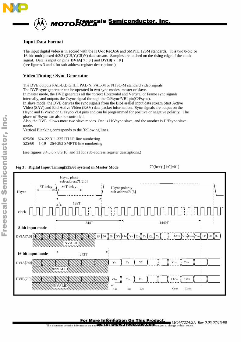
Video Timing / Sync Generator The DVE outputs PAL-B,D,G,H,I, PAL-N, PAL-M or NTSC-M standard video signals.The DVE sync generator can be operated in two sync modes, master or slave. In master mode, the DVE generates all the correct Horizontal and Vertical or Frame sync signals internally, and outputs the Csync signal through the C/Fsync/VBI pin(C/Fsync). In slave mode, the DVE derives the sync signals from the Bit-Parallel input data stream Start Active Video (SAV) and End Active Video (EAV) data packet information. Sync signals are output on the Hsync and F/Vsync or C/Fsync/VBI pins and can be programmed for positive or negative polarity. The phase of Hsync can also be controlled. Also, the DVE allows more two slave modes. One is H/Vsync slave, and the another is H/Fsync slave mode. Vertical Blanking corresponds to the following lines. 625/50 624-22 311-335 ITU-R line numbering 525/60 1-19 264-282 SMPTE line numbering (see figures 3,4,5,6,7,8,9,10, and 11 for sub-address register descriptions.)
Input Data Format The input digital video is in accord with the ITU-R Rec.656 and SMPTE 125M standards. It is two 8-bit or 16-bit multiplexed 4:2:2 ((CB,Y,CR)Y) data stream. Samples are latched on the rising edge of the clock signal. Data is input on pins DVIA[ 7 : 0 ] and DVIB[ 7 : 0 ] (see figures 3 and 4 for sub-address register descriptions.)
6
Fig 3 : Digital Input Timing(525/60 system) in Master Mode 70(hex)[1:0]=01
1440T
Hsync phasesub-address71[2:0]
Hsync
clock
128TT
244T
Hsync polaritysub-address71[5]
+4T delay-3T delay
DVIA[7:0] Cr718Cb718 Y718 Y719 00 00FFCb2Cr0Cb0 Y0 Y1 Y2
INVALID
00 00 XYFF
Y718 Y719
DVIB[7:0] Cr718Cb718Cb2Cr0Cb0
INVALID
DVIA[7:0] Y2Y1Y0
INVALID
16-bit input mode
8-bit input mode
Cb718Cr718Cr2Cr0 Cb0
or
242T
Fre
esc
ale
Se
mic
on
du
cto
r, I
Freescale Semiconductor, Inc.
For More Information On This Product, Go to: www.freescale.com
nc
...

MC44722A/3A Rev 0.05 07/15/98No.
This document contains information on a new product. Specifications and information herein are subject to change without notice.
7
CSYNC
CSYNC
525524 1 2 3 4 5 6 7 8 9 10 11 21 22 23
262261 263 264 265 266 267 268 269 270 271 272 273 283 284 285
Fig 5 : Sync Timing::525/60 Interlaced System in Master Mode
Vsync
Hsync
Vsync
Hsync
sub-address71[7] =0
Fsync
Fsync polaritysub-address71[3]
Vsync polaritysub-address71[4]
Fsync
Fig 4 : Digital Input Timing(625/50 system) in Master Mode 70(hex)[1:0]=01
1440T
Hsync phasesub-address71[2:0]
Hsync
clock
128TT
264T
Hsync polaritysub-address71[5]
+4T delay-3T delay
DVIA[7:0] Cr718Cb718 Y718 Y719 00 00FFCb2Cr0Cb0 Y0 Y1 Y2
INVALID
00 00 XYFF
Y718 Y719
DVIB[7:0] Cr718Cb718Cb2Cr0Cb0
INVALID
DVIA[7:0] Y2Y1Y0
INVALID
16-bit input mode
8-bit input mode
Cb718Cr718Cr2Cr0 Cb0
or
262T
Fre
esc
ale
Se
mic
on
du
cto
r, I
Freescale Semiconductor, Inc.
For More Information On This Product, Go to: www.freescale.com
nc
...

MC44722A/3A Rev 0.05 07/15/98No.
This document contains information on a new product. Specifications and information herein are subject to change without notice.
8
CSYNC
262261 1 2 3 4 5 6 7 8 9 10 11 21 22 23
Fig 7 : Sync Timing::525/60 Non-interlaced System in Master Mode
CSYNC
310 311 312 1 2 3 4 6 7 8 21 22 235309308
Vsync
Hsync
Vsync
Hsync
Fig 8 : Sync Timing::625/50 Non-interlaced System in Master Mode
9
sub-address71[7] =1
Fsync polaritysub-address71[3]
Vsync polaritysub-address71[4]
Fsync
Fsync polaritysub-address71[3]
Vsync polaritysub-address71[4]
Fsync
sub-address71[7] =1
CSYNC
623 624 625 1 2 4 6 7 8 21 22 23
CSYNC
311 312 313 314 315 316 317 318 319 320 321 334 335
5622621
310309
Vsync
Hsync
Vsync
Hsync
Fig 6 : Sync Timing::625/50 Interlaced System in Master Mode
9
Fsync
Fsync polaritysub-address71[3]
Vsync polaritysub-address71[4]
Fsync
sub-address71[7] =0
3
Fre
esc
ale
Se
mic
on
du
cto
r, I
Freescale Semiconductor, Inc.
For More Information On This Product, Go to: www.freescale.com
nc
...

MC44722A/3A Rev 0.05 07/15/98No.
This document contains information on a new product. Specifications and information herein are subject to change without notice.
Fig 10 : Sync Timing::525/60 Interlaced System in Slave Mode
Vsync
Hsync
Fsync
Vsync polaritysub-address71[5]
CSYNC
3 4 5 6 7
Fsync polaritysub-address71[4]
Odd field
CSYNC
Vsync
Hsync
Fsync
266 267 268 269
Even field
sub-address71[1:0] =10, 11
Hsync Delay sub-address 7A[7:0], 71[3:0]
Internal Hsync reset counter
9
Fig 9 : Analog Sync Timing::Rise and fall
2.37uS 29.41uS 27.04uS 4.74uS
0.148uS 0.148uS
63.56uS
NTSC
PAL0.222uS
0.222uS
2.37uS 29.63uS 27.26uS 4.74uS
64.00uS
Fre
esc
ale
Se
mic
on
du
cto
r, I
Freescale Semiconductor, Inc.
For More Information On This Product, Go to: www.freescale.com
nc
...

MC44722A/3A Rev 0.05 07/15/98No.
This document contains information on a new product. Specifications and information herein are subject to change without notice.
10
Fig 11 : Sync Timing::625/50 Interlaced System in Slave Mode
Vsync
Hsync
Fsync
Vsync polaritysub-address71[5]
Fsync polaritysub-address71[4]
Odd field
CSYNC
625 1 2 3 4
CSYNC
Vsync
Hsync
Fsync
313 314 315 316
Even field
sub-address71[1:0] =10, 11
Hsync Delay sub-address 7A[7:0], 71[3:0]
Internal Hsync reset counter
Fre
esc
ale
Se
mic
on
du
cto
r, I
Freescale Semiconductor, Inc.
For More Information On This Product, Go to: www.freescale.com
nc
...

MC44722A/3A Rev 0.05 07/15/98No.
This document contains information on a new product. Specifications and information herein are subject to change without notice.
Chroma / Luma Encoding The DVE de-multiplexes the 4:2:2 digital video data stream. The de-multiplexed Y or Luma samples are interpolated at the clock rate. Offset compensation is then added, next any VBI signals consisting of Closed-Caption, CGMS and WSS are added to the appropriate lines, then finally composite sync pulses are added to the Luma signal.(see figure 14.) De-multiplexed component color CB and CR samples are interpolated at the clock rate. The Luma and Chroma Interpolation filter compensate for the sin(x)/x attenuation to on chip D/A converter and simplify the output filter and allows more accurate encoding. A set of 3 different filters is available for each Luma and Chroma filtering. And user can select within these filters to fit a wide variety of applications. (see figure 12 and 13, and sub-address resister 6F ) The DVE generates the necessary subcarrier color frequency for PAL or NTSC encoding from the 27Mhz system clock. This color subcarrier is then modulated by the base band component color CB and CR signals to create the video Chroma signal. (see figure 15.) A 7.5 IRE pedestal is added for the 60Hz field rate. This can be added for the 50Hz field rate through serial bus control. (see sub-address register descriptions)
11
"CVBS and S-VIDEO" or "YCbCr" Outputs The internal digital video signals drive 10-bit D/A converters. Converter outputs are bidirectional current sources where the current is proportional to the digital data with reference to the IBIAS reference current. The pins CVBS/Cb, Y and C/Cr are the respective composite, Luma and Chroma or Y/Cb/Cr signal current source pins. Each of the DACs can drive 75ohm load resister. User can select 1 sets of signals from the above 2 signal sets (CVBS/Y/C or Y/Cb/Cr ).(see "Application Diagram" and "sub-address register descriptions".) In Y/Cr/Cb analog component output mode, user can select one of the component interface level , Beta Cam or M2 format ( see sub-address register 6E ). Bias Current Gain DACs can be switched off through serial bus control to reduce power consumption. Both outputs of unused DACs should be connected to ground through a resister to avoid charge buildup.
14131211109876543210-48
-45
-42
-39
-36
-33
-30
-27
-24
-21
-18
-15
-12
-9
-6
-3
0
3
6
Frequency [MHz]
Am
plit
ude
[dB
]
Fig. 12 Luma Filtering Including DAC Attenuation
14131211109876543210-48
-45
-42
-39
-36
-33
-30
-27
-24
-21
-18
-15
-12
-9
-6
-3
0
3
6
Frequency [MHz]
Am
plit
ude
[dB
]
f1 = 6MHz
f2 = 5MJz
f3 = 2.5MHzf1 = 3MHz
f2 = 2.5MHz
f3 = 1.5MHz
Fig. 13 Chroma Filtering
Fre
esc
ale
Se
mic
on
du
cto
r, I
Freescale Semiconductor, Inc.
For More Information On This Product, Go to: www.freescale.com
nc
...

MC44722A/3A Rev 0.05 07/15/98No.
This document contains information on a new product. Specifications and information herein are subject to change without notice.
Fig 14 : Luminance Output Range
12
106
16
235210
170145
81
41
16
Digital Y input code(16~235) 525/60 and 625/50 system100%amplitude,100%saturation color bar
0
11
30
41
597089
100
-33
IRE
670620
540490
412
362
282232
44
200
0
code1023
0
11
30
41
597089
100
-43
IRE
670620
540490
412
362
282
232
44
232
Analog Y output level(625/50 system)100%amplitude,100%saturation color bar=> 7.5IRE Setup Off
0
code1023
232
07.5
30
41
5970
89100
-40
IRE
670620
540490
412
362
282232
56
Analog Y output level(525/60 system)100%amplitude,100%saturation color bar=> 7.5IRE Setup Off
0
code1023
232
11
07.5
30
41
5970
89100
-40
IRE
670620
540490
412
362
282232
12
Analog Y output level(525/60 system)100%amplitude,100%saturation color bar=> 7.5IRE Setup On
0
code1023
23211200
Analog Y output level(625/50 system)100%amplitude,100%saturation color bar=> 7.5IRE Setup On
Fre
esc
ale
Se
mic
on
du
cto
r, I
Freescale Semiconductor, Inc.
For More Information On This Product, Go to: www.freescale.com
nc
...

MC44722A/3A Rev 0.05 07/15/98No.
This document contains information on a new product. Specifications and information herein are subject to change without notice.
13
Fig 15 : Chrominance Output Range
146128
1634
222240
110
128
Digital Cr-input code(16~240) 525/60 and 625/50 system100%amplitude,100%saturation color bar
Digital Cb-input code(16~240) 525/60 and 625/50 system100%amplitude,100%saturation color bar
16
166
54
202
90
240
128 128
± 228
± 324 ± 302 ± 324
± 228
± 110
± 302
-63
-48
-21.5
21.5
486367
IRE
Analog C output level(625/50 system)100%amplitude,100%saturation color bar=> 7.5IRE Setup On/Off
-67
0
code
512
0
1023
IRE
Analog C output level(525/60 system)100%amplitude,100%saturation color bar=> 7.5IRE Setup Off/On
-59-45
-20
20
455963
-63
0
± 228
± 324 ± 302 ± 324
± 228
± 110
± 302
code
512
0
1023
Fre
esc
ale
Se
mic
on
du
cto
r, I
Freescale Semiconductor, Inc.
For More Information On This Product, Go to: www.freescale.com
nc
...

MC44722A/3A Rev 0.05 07/15/98No.
This document contains information on a new product. Specifications and information herein are subject to change without notice.
Fig 16 : Y/Cb/Cr Output Range ( Beta Cam Component Interface Level )
14
584512
64136
888
960
440
512
Digital Cr-input code100%amplitude,100%saturation color bar=> 7.5IRE Setup On/Off
IRE
0
code1023
-59-45
-20
20
455963
-63
0 512
64
664
216
808
360
960
512 512
-63
-48
-21.5
21.5
48
63
IRE
0
code
512
0
1023
Digital Cb-input code100%amplitude,100%saturation color bar=> 7.5IRE Setup On/Off
670620
540490
412
362
282232
12
200
0
code1023 IRE
670620
540490
412
362
282
232
56
232
Analog Y output level100%amplitude,100%saturation color bar=> 7.5IRE Setup Off
0
code1023
232
IRE
07.5
30
41
5970
89100
-40
11
0
30
41
5970
89100
-40
11
Analog Y output level100%amplitude,100%saturation color bar=> 7.5IRE Setup On
Fre
esc
ale
Se
mic
on
du
cto
r, I
Freescale Semiconductor, Inc.
For More Information On This Product, Go to: www.freescale.com
nc
...

MC44722A/3A Rev 0.05 07/15/98No.
This document contains information on a new product. Specifications and information herein are subject to change without notice.
Fig 17 : Y/Cb/Cr Output Range ( M2 Component Interface Level )
15
584512
64
136
888
960
440
512
Digital Cr-input code 100%amplitude,100%saturation color bar=> 7.5IRE Setup On/Off
IRE
0
code1023
-59-45
-20
20
455963
-63
0 512
64
664
216
808
360
960
512 512
-63
-48
-21.5
21.5
48
63
IRE
0
code
512
0
1023
Digital Cb-input code100%amplitude,100%saturation color bar=> 7.5IRE Setup On/Off
0
11
30
41
5970
89100
-43
IRE
670620
540490
412
362
282
232
44
232
Analog Y output level100%amplitude,100%saturation color bar=> 7.5IRE Setup Off
0
code1023
0
11
30
41
5970
89100
-33
IRE
670620
540490
412
362
282232
44
200
Analog Y output level100%amplitude,100%saturation color bar=> 7.5IRE Setup On
0
code1023
232
Fre
esc
ale
Se
mic
on
du
cto
r, I
Freescale Semiconductor, Inc.
For More Information On This Product, Go to: www.freescale.com
nc
...

MC44722A/3A Rev 0.05 07/15/98No.
This document contains information on a new product. Specifications and information herein are subject to change without notice.
Closed-Caption Encoding Closed-Captioned or Extended Data Service signals can be encoded by the DVE onto output video line 21/284 (NTSC) and line 22/335 (PAL). The CC data is input through the serial bus interface. Two 8-bit byte data pairs are encoded for each field. There are four registers for holding the data - two bytes per field. The serial data is 7bit US-ASCII MSB first, proceeded by an odd parity bit. Total 8-bits. (P-7-6-5-4-3-2-1-0)
The DVE automatically generates the required clock run in and start bit for CC encoding. (see figure 16.)When Closed-Captioning is enabled, the system micro processor (uP) should update the CC data once each frame. This DVE will automatically NULL characters when there is no CC data to encoder after the CC data has been processed by setting the $87[5] register.
It is recommended to write CC data only to the inactive frame. Field1 and Field2 data are double-buffered by the Frame sync falling edge of previous Frame, updating Frame 2 data during Frame1 display and Frame1 data during Frame2 display.
When the $87[4] register is set, the DVE will generate the parity bit automatically. (see figures 26 and 27 for sub-address register descriptions.)
Copy Generation Management System (CGMS) Encoding CGMS signals can be encoded by the DVE onto output video line 20 (525 / 60 for Japan). CGMS identification signals also identify and control the TV screen presentation mode - wide screen, letter box and or normal -16:9 or 4:3. Data is Double-Buffered and is latched at the start of Field 1.
CRC code is generated by controling $88 [ 0 ] CGMS_parity bit automatically.
(see figures 24 for sub-address register descriptions.)
16
Wide Screen Signaling (WSS) Encoding WSS signals can be encoded by the DVE onto output video line 23 (625 / 50 for Europe). WSS identification signals also identify and control the TV screen presentation mode - wide screen, letter box and or normal -16:9 or 4:3. Data is Double-Buffered and is latched at the start of Field 1.
Odd parity code is generated by controling $88 [ 1 ] WSS_parity bit automatically. (see figures 25 for sub-address register descriptions.)
Fre
esc
ale
Se
mic
on
du
cto
r, I
Freescale Semiconductor, Inc.
For More Information On This Product, Go to: www.freescale.com
nc
...

MC44722A/3A Rev 0.05 07/15/98No.
This document contains information on a new product. Specifications and information herein are subject to change without notice.
Serial Control Bus Control of the DVE device is accomplished through the I2C-Bus or 4-wired SPI serial bus. In I2C mode, pins SDA and SCL are the respective data and clock signals. Device address can be 42(hex)/43(hex) or 1C(hex)/1D(hex) . Slave address is chosen at reset by the state of the ChipA pin signal 0 : 42(hex)/43(hex), 1 : 1C(hex)/1D(hex) Sub-address register read and write operations are documented in the following figures 22a - 22b. In SPI mode, pins SO, SI, SCK and SEL are the respective data input, output, serial clock and chip select signals. Register read and write operations are documented in the following figures 23a - 23b
17
MACROVISIONTM Copy Protection When enabled, the Luma and Chroma signals are modified according to the MACROVISION TM copy protection process for Pay Per View (PPV) and DVD applications revision 7.01 dated Sep 6th , 1996. Enabling and control is through the serial control bus. No MC44722A parts will be sent to the customer until the customer provides MOTOROLA with written confirmation of a license, non-disclosure or a waiver from MACROVISION TM. The MC44723A device is available without MACROVISION TM encoding.
Fre
esc
ale
Se
mic
on
du
cto
r, I
Freescale Semiconductor, Inc.
For More Information On This Product, Go to: www.freescale.com
nc
...

MC44722A/3A Rev 0.05 07/15/98No.
This document contains information on a new product. Specifications and information herein are subject to change without notice.
18
Fig 18-a : I2C-BUS Interface Write operation Timing
MSB
D7 D6 D5 D4 D3 D2 D1 D0
LSB
SCL
SDAMSB
D7 D6 D5 D4 D3 D2 D1 D0
LSB
MSB
D7 D6 D5 D4 D3 D2 D1 D0
LSB
SCL
SDA
MSB
D7 D6 D5 D4 D3 D2 D1 D0
LSB
Start chip address(write) ACK Sub-address
Data 1 Data NACK ACK
ACK
Stop
MSB
D7 D6 D5 D4 D3 D2 D1 D0
LSB
SCL
SDAMSB
D7 D6 D5 D4 D3 D2 D1 D0
LSB
MSB
D7 D6 D5 D4 D3 D2 D1 D0
LSB MSB
D7 D6 D5 D4 D3 D2 D1 D0
LSB
Start chip address(write) ACK Sub-address
Data 1ACK ACK by MCU
ACK Stop
SCL
SDA
Start chip address(Read)
MSB
D7 D6 D5 D4 D3 D2 D1 D0
LSB MSB
D7 D6 D5 D4 D3 D2 D1 D0
LSB
Data NACK by MCU
ACK by MCU
Stop
SCL
SDA
Data 2
Fig 18-b : I2C-BUS Interface Read operation Timing
Fre
esc
ale
Se
mic
on
du
cto
r, I
Freescale Semiconductor, Inc.
For More Information On This Product, Go to: www.freescale.com
nc
...

MC44722A/3A Rev 0.05 07/15/98No.
This document contains information on a new product. Specifications and information herein are subject to change without notice.
19
Fig 19-a : SPI-BUS Interface Write operation Timing
MSB
D7 D6 D5 D4 D3 D2 D1 D0
LSB
SCK
SIMSB
D7 D6 D5 D4 D3 D2 D1 D0
LSB
MSB
D7 D6 D5 D4 D3 D2 D1 D0
LSB
SCK
SI
MSB
D7 D6 D5 D4 D3 D2 D1 D0
LSB
Start Write Command Sub-address
Data 1 Data N
SEL
x
SEL
MSB
x x x x x x x x
LSB
SO(Don't care) MSB
x x x x x x x x
LSB
x
MSB
D7 x x x x x x x
LSB
SO(Don't care) MSB
x x x x x x x x
LSB
Fre
esc
ale
Se
mic
on
du
cto
r, I
Freescale Semiconductor, Inc.
For More Information On This Product, Go to: www.freescale.com
nc
...

MC44722A/3A Rev 0.05 07/15/98No.
This document contains information on a new product. Specifications and information herein are subject to change without notice.
MSB
D7 D6 D5 D4 D3 D2 D1 D0
LSB
SCK
SIMSB
D7 D6 D5 D4 D3 D2 D1 D0
LSB
MSB
D7 D6 D5 D4 D3 D2 D1 D0
LSB MSB
x x x x x x x x
LSB
Start Write Command Sub-address
Data 1
Stop
SCK
SI
Start Read Command
MSB
x x x x x x x x
LSB MSB
x x x x x x x x
LSB
Data N Stop
SCK
SI
Data 2
Fig 19-b : SPI-BUS Interface Read operation Timing
SEL
x
MSB
x x x x x x x x
LSB
SO(Don't care) MSB
x x x x x x x x
LSB
x
SEL
x
MSB
x x x x x x x x
LSB MSB
D7 D6 D5 D4 D3 D2 D1 D0
LSBSO x
SEL
MSB
D7 D6 D5 D4 D3 D2 D1 D0
LSB MSB
D7 D6 D5 D4 D3 D2 D1 D0
LSBSO
20
Fre
esc
ale
Se
mic
on
du
cto
r, I
Freescale Semiconductor, Inc.
For More Information On This Product, Go to: www.freescale.com
nc
...

MC44722A/3A Rev 0.05 07/15/98No.
This document contains information on a new product. Specifications and information herein are subject to change without notice.
21
[Specifications]
DAC Blocks Characteristics(Power Supply 5.0V,Ta=25°C) Characteristics Sym. Min Typ Max Unit Other Resolution - - - 10 Bit Integral Non-Linearity INL - - ± 2.0 LSB Vref = 1.5V, Ibias = 1.8kΩ, Rl = 180Ω Differential Non-Linearity DNL - - ± 1.0 LSB Vref = 1.5V, Ibias = 1.8kΩ, Rl = 180Ω Analog Output Voltage Vyo 1.35 1.5* 1.65 Vp-p Vref = 1.5V, Ibias = 1.8kΩ, Rl = 180Ω Full Scale Output Voltage Vyfs 1.35 1.5** 1.65 V Vref = 1.5V, Ibias = 1.8kΩ, Rl = 180Ω Zero Scale Output Voltage Vyzs - 0.0*** 0.1 V Vref = 1.5V, Ibias = 1.8kΩ, Rl = 180Ω External Load Resistance R L 75 - - Ω
DAC Blocks Characteristics(Power Supply 3.3V,Ta=25°C) Characteristics Sym. Min Typ Max Unit OtherResolution - - - 10 BitIntegral Non-Linearity INL - - ± 2.0 LSB Vref = 1.0V, Ibias = 1.8kΩ, Rl = 180ΩDifferential Non-Linearity DNL - - ± 1.0 LSB Vref = 1.0V, Ibias = 1.8kΩ, Rl = 180ΩAnalog Output Voltage Vyo 0.85 1.00* 1.15 Vp-p Vref = 1.0V, Ibias = 1.8kΩ, Rl = 180ΩFull Scale Output Voltage Vyfs 0.85 1.00** 1.15 V Vref = 1.0V, Ibias = 1.8kΩ, Rl = 180Ω Zero Scale Output Voltage Vyzs - 0.0*** 0.1 V Vref = 1.0V, Ibias = 1.8kΩ, Rl = 180Ω External Load Resistance RL 75 - - Ω
Note : D/A Converter Output Full Scale Voltage
Vyts (V) = (Vref / Iref ) * K * R load (K = 10 : DAC Current Gain) ( code 3ff(fex))
Power Dissipation
Pd = [ (Vref/Iref * 10 * 3ch) + 10mA (Bais Current)] * 3.3V (or 5V)
Electrical Characteristics Characteristic Symbol Min Typ Max Unit Other Power Supply Voltage(Analog Blocks) AVDD 3.1 3.3 3.5 V DAVDD 4.75 5.0 5.25Power Supply Voltage(Digital Blocks) DVDD 3.1 3.3 3.5 V DVDDSupply Current(Analog Blocks) AIcc - 70 - mA Vref = 1.0V, Supply Current(Digital Blocks) DIcc - 50 - mA Iref = 1.8KΩ, Rl = 180ΩOperating Temperature Ta 0 - 70 °C
* : code 000(hex) ~code max.** : code max.*** : code 000(hex)
* : code 000(hex) ~code max.** : code max.*** : code 000(hex)
Maximum Ratings DC Supply Voltage Vdd -0.5 ~ +7.0 V Input Voltage, All Inputs Vin -1.5 ~ Vdd+1.5 VOutput Voltage, All Outputs Vout -0.5 ~ Vdd+1.5 VDC Output Current, per Pin Iout 25 mAPower Dissipation Pd 750 mWStorage Temperature Tstg -65 ~ +150 °C
Other -1.5 ~ Vdd+1.95V at Vdd=3.3V
Fre
esc
ale
Se
mic
on
du
cto
r, I
Freescale Semiconductor, Inc.
For More Information On This Product, Go to: www.freescale.com
nc
...

MC44722A/3A Rev 0.05 07/15/98No.
This document contains information on a new product. Specifications and information herein are subject to change without notice.
22
Tds
50%
TdhTr Tf
Clock
Input Data
50%
validnot valid not valid
Clock Blocks Characteristics Characteristic Symbol Min Typ Max Unit
Clock Rate fc - 27.0 - MHz Clock Duty Cycle Dty 45 50 55 %
Digital Blocks Electrical Characteristics(Power Supply 3.3V,Ta=25°C ± 3°C) Characteristics Symbol Min Typ Max Unit
Input Voltage HIGH ViH 2.0 - 5.25 V LOW ViL - - 0.8 V
Output Voltage HIGH VoH 2.4 - - V(2.0mA) LOW VoL - - 0.4 V
Input Leakage Current Iin - ±2.5 - µAHi-Z Leakage Current Ioz - ±20 - µAInput Capacitance Cin - - 20 pFLoad Capacitance CL - - 20 pFData Setup Time Tds 4 - - nSData Hold Time Tdh 5 - - nSInput Rise Time Tr - - 5 nSInput Fall Time Tf - - 5 nSData delay Td - - 27 nS
[Specifications]
I2C/SPI-BUS Blocks Characteristics(Power Supply 3.3V,Ta=25°C ± 3 °C) Characteristics Symbol Min Typ Max Unit Input Voltage LOW VILM - - 0.8 VInput Voltage High VIHM 2.3 - 5.25 VInput Current VIM - - ± 10 µASDA Output Voltage (I OM=3mA) VOM - - 0.4 VOutput Current (during acknowledge) IOM 3 - - mASPI Maxmum Clock Rate fspi - - 3 MHz
Fre
esc
ale
Se
mic
on
du
cto
r, I
Freescale Semiconductor, Inc.
For More Information On This Product, Go to: www.freescale.com
nc
...

MC44722A/3A Rev 0.05 07/15/98No.
This document contains information on a new product. Specifications and information herein are subject to change without notice.
[I2C-BUS Slave Address 42(hex)/43(hex) or 1C(hex)/1D(hex)]
<I2C-Bus Format>
WRITE MODE
DATA NDATA 0Sub AddressSlave Address --------S A A A A P
if more than 1byte DATA is transmitted,then auto-increment of the Sub Address is performed
S Start conditionSlave Address 42(hex) or 1C(hex)A Acknowledge, generated by the slaveSub Address Sub address byteDATA 0 First data byteDATA N continued data byte(Sub Address is auto increment)P Stop condition
READ MODE
Slave Address Sub Address NS A A P
Slave AddressS A PDATA N AM DATA N + 1 AM ------ AM
then
Slave receiver
Slave transmitter
42(hex) or 1C(hex)
43(hex) or 1D(hex)
42(hex) or 1C(hex)
S Start conditionSlave Address Slave receiver is act transmitter is adA Acknowledge, generated by the slaveSub Address N Sub Address byteDATA N DATA byte of Register NDATA N + 1 DATA byte of Register N + 1 (address auto-increment)AM Acknowledge, generated by the micro controllerP Stop condition (When Last AM must be '1' )
23
Fre
esc
ale
Se
mic
on
du
cto
r, I
Freescale Semiconductor, Inc.
For More Information On This Product, Go to: www.freescale.com
nc
...

MC44722A/3A Rev 0.05 07/15/98No.
This document contains information on a new product. Specifications and information herein are subject to change without notice.
<SPI-Bus Format>
WRITE MODE
DATA NDATA 0Sub AddressWrite Command --------S P
if more than 1byte DATA is transmitted,then auto-increment of the Sub Address is performed
S Chip select on ( Hi to Lo)Write Command 42(hex) or 1C(hex)Sub Address Sub address byteDATA 0 First data byteDATA N continued data byte(Sub Address is auto increment)P Chip select off (Lo to Hi)
READ MODE
Write Command Sub Address NS P
Read CommandS PDATA N DATA N + 1 ---------
then
Slave receiver
Slave transmitter
42(hex) or 1C(hex)
43(hex) or 1D(hex)
42(hex) or 1C(hex)
S Chip select on (Hi to Lo)Sub Address N Sub Address byte setRead Command 43(hex) or 1D(hex)DATA N DATA byte of Register NDATA N + 1 DATA byte of Register N + 1 (address auto-increment)P Chip select off (Lo to Hi)
24
[SPI-BUS]
Fre
esc
ale
Se
mic
on
du
cto
r, I
Freescale Semiconductor, Inc.
For More Information On This Product, Go to: www.freescale.com
nc
...

MC44722A/3A Rev 0.05 07/15/98No.
This document contains information on a new product. Specifications and information herein are subject to change without notice.
Y Fil mode 0 : Luma Filter switch 0 : wide 6MHz (default)1 : narrow 2.5Mhz
V Fil, U Fil mode0 : Chroma Filter switch0 : wide 3.0MHz(default)1 : narrow 1.5MHz
Cr Fil, Cb Fil mode 0 : Cr/Cb Filter switch0 : wide 3.0MHz(default)1 : narrow 1.5MHz
Cr /Cb Fil mode 1 : wide Filter switch0 : wide0 3.0MHz(default)1 : wide1 2.5MHz
Y Fil mode 1 : wide Filter switch0 : wide0 6.0MHz(default)1 : wide1 5MHz
Sub-address 6F : Interpolation Filter Switch (write)
MSB LSB
Register 6F
default : 0000_0000(bin)
V Filmode0
Y Filmode0
U Filmode0
Cr Filmode0
Cb Filmode0
Cb/Cr/U/V Fil mode1
Y Filmode1-
25
M2/Beta : Y select M2 type, BetaCam type00 : BetaCam (default)*01 : M2 ( 7.5IRE setup )*10 : BetaCam ( 7.5IRE setup )*
11 : M2* Note * : These bit can related w/ sub address $72 [ 4 ] setup bit.
Y mode : Separate switch0 : Y/CbCr's Y is same as Y/C/CVBS's Y (default)1 : Y/CbCr's Y is the BetaCam or M2 Y signal
CbCr gain : Cb/Cr gain0 : normal operation (default)1 : 1/2 gain (disable code divided by 2)
[Register Mapping and Description]
Sub-address 6E : Y/CbCr mode setup (write)
MSB LSB
Register 6ECbCr mode
Y mode M2/Beta[0]
default : 0000_0000(bin)
M2/Beta[1]- - - -
Fre
esc
ale
Se
mic
on
du
cto
r, I
Freescale Semiconductor, Inc.
For More Information On This Product, Go to: www.freescale.com
nc
...

MC44722A/3A Rev 0.05 07/15/98No.
This document contains information on a new product. Specifications and information herein are subject to change without notice.
26
Sub-address 70 : Variable I/O Switch (write/read)
MSB LSB
Register 70 bs-off self-SW color barselect VBLK SW
C/Fsync SW
default : 0000_0001(bin)
F/Vsync SW
M/Smode1
M/Smode0
bs - off : color burst control switch On/Off0 : color burst ON (default)1 : color burst OFF
self - SW : internal self H/V counter reset switch On / Off0 : self counter reset OFF (default)1 : self counter reset ON
Note : this mode is ONLY valid at when 70h[1: 0] is "10(bin)" or "11(bin)".
color bar select : color bar selectLuma Chroma
0 : color bar 100% 75%1 : color bar 100% 100%
VBLK SW : Vertical Blanking Mask Enable switch On-Off0 : reject VBI information data in vertical blanking period (default)1 : through VBI information data in vertical blanking period
C/Fsync SW : Composite sync/Frame sync output switch0 : Frame sync output (default)1 : composite sync output
F/Vsync SW : Frame sync /Vertical sync output switch0 : Vertical sync output (default)1 : Frame sync output
M/S sync mode1 : Master or Slave sync mode M/S sync mode0 00 : 601 H/V master mode
01 : 656 slave mode(no H/Vsync output) (default)10 : Fsync/Hsync slave mode11 : Vsync/Hsync slave mode
Fre
esc
ale
Se
mic
on
du
cto
r, I
Freescale Semiconductor, Inc.
For More Information On This Product, Go to: www.freescale.com
nc
...

MC44722A/3A Rev 0.05 07/15/98No.
This document contains information on a new product. Specifications and information herein are subject to change without notice.
Sub-address 71 : Sync control (write/read)
MSB LSB
Register 71 non-inter VBI SW h-polarity v-polarity
default : 0000_0100(bin)
f-polarity h- delay2 h-delay1 h-delay0
non-inter : non-interlaced mode select0 : interlace mode (default)1 : non-interlace mode
VBI SW : vertical blanking information signal input control switch on 34 pin0 : VBI input Off (default)1 : VBI input On
h-polarity : polarity of Hsync0 : negative (default)1 : positive
v-polarity : polarity of Vsync0 : negative (default)1 : positive
f-polarity : polarity of Fsync0 : field1 (odd) = low level (default)1 : field1 (odd) = high level
h-delay2 : delay on Hsync with reference to DVIA/DVIB data in Master mode h-delay1 000: + 4 clock delay h-delay0 001: + 3 clock delay
010: + 2 clock delay011: + 1 clock delay100: + 0 clock delay101: - 1 clock delay110: - 2 clock delay111: - 3 clock delay
Note : this h-delay can be also related with 7A[7:0] register and can delay totally +2023 clock delay in H/V or H/Fsync slave mode.
27
Fre
esc
ale
Se
mic
on
du
cto
r, I
Freescale Semiconductor, Inc.
For More Information On This Product, Go to: www.freescale.com
nc
...

MC44722A/3A Rev 0.05 07/15/98No.
This document contains information on a new product. Specifications and information herein are subject to change without notice.
Sub-address 72 : PAL/NTSC setup (write / read)
MSB LSB
Register 72 phase-set C/Fsync/VBII/O SW color bar setup75 625/525 PAL/
NTSC2PAL/NTSC1
default : 0000_1000(bin) NTSC (If "PAL/NTSC" pin is LOW level)0000_0101(bin) PAL
TEST
phase-set : color sub-carrier phase synchronization 0 : free running (default)1 : 1 phase reset/8 field and 1 phase reset/4 frame
TEST : for test, should be "0"
C/Fsync/VBI : Input/Output switch on 34 pin (C/Fsync/VBI pin ) I/O SW 0 : VBI input(default)
1 : Csync or Frame sync output
color bar : internal color bar generator control0 : normal operation (default)1 : color bar generator On (need to set color bar mode on sub-address 70[5]. )
setup75 : Setup level for Luminance 0 : setup level for luminance = 0IRE1 : setup level for luminance = 7.5IRE
625/525 : control line mode0 : 525 lines / 60 Hz mode1 : 625 lines / 50 Hz mode
PAL/NTSC2 : subcarrier control PAL/NTSC1 00 : NTSC(M)
01 : PAL (BDGHI)10 : PAL (M)11 : PAL (N)
28
Fre
esc
ale
Se
mic
on
du
cto
r, I
Freescale Semiconductor, Inc.
For More Information On This Product, Go to: www.freescale.com
nc
...

MC44722A/3A Rev 0.05 07/15/98No.
This document contains information on a new product. Specifications and information herein are subject to change without notice.
29
Sub-address 73: Vertical Blanking Information Luma (Y) Level (write only)
MSB LSB
Y7 Y6 Y5 Y4 Y3 Y2 Y1 Y0Register 73
MSB LSB
V3 V2 V1 V0V6 V5 V4Register 75 V7
Sub-address 75: Burst Chroma (V) Level (write only)
default : 1000_0000(bin)
MSB LSB
U7 U6 U5 U4 U3 U2 U1 U0Register 74
Sub-address 74: Burst Chroma (U) Level (write only)
default : 77(dec) (NTSC) 89(dec) (PAL)
default : 128(dec) (NTSC)155(dec) (PAL)
Fre
esc
ale
Se
mic
on
du
cto
r, I
Freescale Semiconductor, Inc.
For More Information On This Product, Go to: www.freescale.com
nc
...

MC44722A/3A Rev 0.05 07/15/98No.
This document contains information on a new product. Specifications and information herein are subject to change without notice.
30
Sub-address 76 : DAC set 1 signal control (write only)
MSB LSB
Register 76 Cr Cb Luma dac 1pin
default : 0000_0000(bin)
dac 7pin dac 4pin
Cr : Cr/Cb signal control (Data path enable) Cb 0 : Cr, Cb On (default)
1 : chrominance Off
Luma : Luminance control (Data path enable)0 : luminance On (default)1 : luminance Off
dac 1pin : D/A converter (1) output On-Off control dac 4pin 0 : CVBS/Cb DAC, C/Cr DAC, Y DAC output On (default)dac 7pin 1 : CVBS/Cb DAC, C/Cr DAC, Y DAC output Off
dac set 1 mode : 1~9-pin's D/A converter output signal control 10 : Y/Cr/Cb output On
00 : Y/C/CVBS output On
dac set 1mode[0]
Sub-address 77 : reserved
MSB LSB
Register 77 - - - - - - -
dac set 1mode[1]
-
Fre
esc
ale
Se
mic
on
du
cto
r, I
Freescale Semiconductor, Inc.
For More Information On This Product, Go to: www.freescale.com
nc
...

MC44722A/3A Rev 0.05 07/15/98No.
This document contains information on a new product. Specifications and information herein are subject to change without notice.
31
Sub-address 78~79 : Sub-carrier phase control (write only)
sc-ph9 : sub-carrier phase controlsc-ph8 00_0000_0000 : sub-carrier phase 0 degree (default)sc-ph7 to sc-ph6 11_1111_1111 : sub-carrier phase 359 degreesc-ph5sc-ph4sc-ph3sc-ph2sc-ph1sc-ph0
MSB LSB
Register 78 sc-ph9 sc-ph8 sc-ph7 sc-ph6
default : 0000_0000(bin)
sc-ph5
MSB LSB
Register 79
default : 0000_0000(bin)
sc-ph4 sc-ph3 sc-ph2
sc-ph1 sc-ph0 - - - - - -
Fre
esc
ale
Se
mic
on
du
cto
r, I
Freescale Semiconductor, Inc.
For More Information On This Product, Go to: www.freescale.com
nc
...

MC44722A/3A Rev 0.05 07/15/98No.
This document contains information on a new product. Specifications and information herein are subject to change without notice.
32
Sub-address 7B : Digital Video Input Select Control (write only)
MSB LSB
Register 7B - -
default : 0000_0000(bin)
Y_tmg
Cr_tmg : Cr clock timing delay in 16-bit Digital Input Mode 00 : Cr clock delay 0 clock (default)01 : Cr clock delay +1 clock10 : Cr clock delay +2 clock11 : Cr clock delay +3 clock (See fig 3,4 )
Cb_tmg : Cb clock timing delay in 16-bit Digital Input Mode 00 : Cb clock delay 0 clock (default)01 : Cb clock delay +1 clock10 : Cb clock delay +2 clock11 : Cb clock delay +3 clock (See fig 3,4 )
Y_tmg : Y clock timing delay in 16-bit Digital Input Mode 0 : Y clock delay 0 clock (default)1 : Y clock delay +1 clock
16-bit : 16-bit YY / CbCr Digital Video Input mode input mode 0 : 8-bit Multiplexed CbYCrY Digital Video Input mode (default)
1 : 16-bit YY / CbCr Digital Video Input mode
16-bit input modeCb_tmg[0]
h-delay10 : delay on Hsync with reference to DVIA/DVIB datah-delay9 0000_0000_000 : Hsync delay 0 delayh-delay8 to h-delay7 1111_1111_000 : Hsync delay +255 delayh-delay6h-delay5h-delay4h-delay3
Note : this h-delay can be also related with 71[3:0] register and can delay totally +2023 delay(1111_1111_111) in H/V or H/Fsync
slave mode.
Sub-address 7A : Hsync delay control (write only)
MSB LSB
Register 7A H-delay10 H-delay9 H-delay8 H-delay7
default : 0000_0000(bin)
H-delay6 H-delay5 H-delay4 H-delay3
Cb_tmg[1]Cr_tmg[0]Cr_tmg[1]
Fre
esc
ale
Se
mic
on
du
cto
r, I
Freescale Semiconductor, Inc.
For More Information On This Product, Go to: www.freescale.com
nc
...

MC44722A/3A Rev 0.05 07/15/98No.
This document contains information on a new product. Specifications and information herein are subject to change without notice.
33
Sub-address 7C : signal control 3(write only)
Y sync : Y sync Signal On/Off (Y/Cb/Cr mode only)0 : Y sync On (default)1 : Y sync Off
CbCr bf : CbCr burst On/Off0 : Cb/Cr bf data Off1 : Cb/Cr bf data On
Chroma bf : Chroma burst On/Off0 : Chroma bf data On1 : Chroma bf data off
MSB LSB
Register 7C Ysync - - -
default : 0000_0000(bin)
- - CbCr bf Chroma bf
Fre
esc
ale
Se
mic
on
du
cto
r, I
Freescale Semiconductor, Inc.
For More Information On This Product, Go to: www.freescale.com
nc
...
MC44722A/3A Rev 0.05 07/15/98No.
This document contains information on a new product. Specifications and information herein are subject to change without notice.
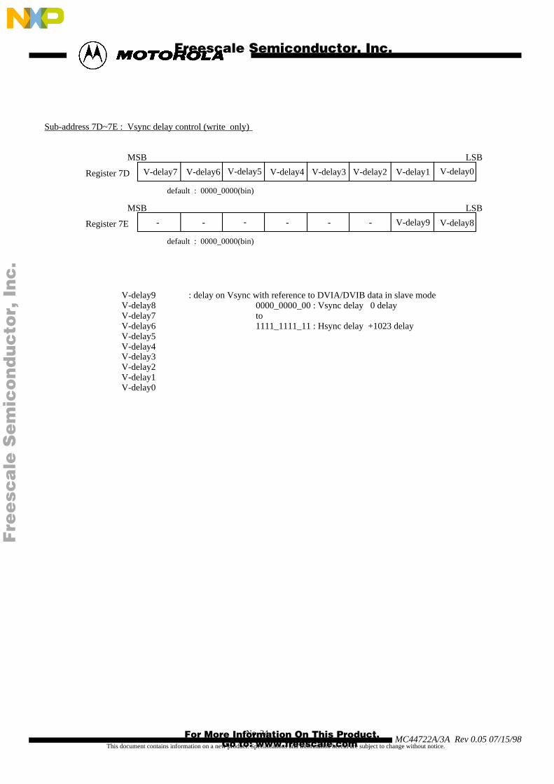
V-delay9 : delay on Vsync with reference to DVIA/DVIB data in slave mode V-delay8 0000_0000_00 : Vsync delay 0 delayV-delay7 to V-delay6 1111_1111_11 : Hsync delay +1023 delayV-delay5V-delay4V-delay3V-delay2V-delay1V-delay0
34
Sub-address 7D~7E : Vsync delay control (write only)
MSB LSB
Register 7D V-delay7 V-delay6 V-delay5 V-delay4
default : 0000_0000(bin)
V-delay3 V-delay2 V-delay1 V-delay0
MSB LSB
Register 7E - - - -
default : 0000_0000(bin)
- - V-delay9 V-delay8
Fre
esc
ale
Se
mic
on
du
cto
r, I
Freescale Semiconductor, Inc.
For More Information On This Product, Go to: www.freescale.com
nc
...

MC44722A/3A Rev 0.05 07/15/98No.
This document contains information on a new product. Specifications and information herein are subject to change without notice.
MSB LSB
XX XX XXRegister 82
Sub-address 80~82: CGMS characters for Field1(Line20)/Field2(Line283) (write only) NTSC only
MSB LSB
cgms7 cgms6 cgms5 cgms4 cgms3 cgms2 cgms1 cgms0
MSB LSB
Register 80
Register 81
b8 b7 b6 b5 b4 b3 b2 b1
b16 b15 b14 b13 b12 b11 b10 b9
b20 b19 b18 b17
XX
2.235 µS
49.1 µS
b1Ref b2 b3 b4 b5 b6 b7 b8 b9 b10b11
b12b13
b14b15
b16b17
b18b19
b20
70IRE
0IRE
-40IRE
Fig 20 : CGMS wave form
35
Fig 21 : WSS wave form
11.0 µS 27.4 µS
38.4 µS44.5 µS
Sub-address 80~81: WSS characters for Line23 (write only) PAL only
MSB LSB
wss7 wss6 wss5 wss4 wss3 wss2 wss1 wss0
MSB LSB
- - wss13 wss12 wss11 wss10 wss9 wss8
Register 80
Register 81
b8 b7 b6 b5 b4 b3 b2 b1
b16 b15 b14 b13 b12 b11 b10 b9
500mV
cgms15 cgms14 cgms13 cgms12 cgms11 cgms10 cgms9 cgms8
cgms19 cgms18 cgms17 cgms16
11.2 µS
Fre
esc
ale
Se
mic
on
du
cto
r, I
Freescale Semiconductor, Inc.
For More Information On This Product, Go to: www.freescale.com
nc
...

MC44722A/3A Rev 0.05 07/15/98No.
This document contains information on a new product. Specifications and information herein are subject to change without notice.
Sub-address 83~84 :closed caption characters/extended data for Field1(Line21) (write)
First byte to Encode
Register 83
Register 84
ccp118 ccb117 ccb116 ccb115 ccb114 ccb113 ccb112 ccb111
ccp128 ccb127 ccb126 ccb125 ccb124 ccb123 ccb122 ccb121
MSB LSB
MSB LSBSecond byte to Encode
parity b7 b6 b5 b4 b3 b2 b1
parity b7 b6 b5 b4 b3 b2 b1
Register 85
Register 86
ccp218 ccb217 ccb216 ccb215 ccb214 ccb213 ccb212 ccb211
ccp228 ccb227 ccb226 ccb225 ccb224 ccb223 ccb222 ccb221
MSB LSB
MSB LSB
Sub-address 85~86 :closed cation character/extended data for Field2(Line284)
First byte to Encode
Second byte to Encode
parity b7 b6 b5 b4 b3 b2 b1
parity b7 b6 b5 b4 b3 b2 b1
36
10.50 µS12.91 µS
4.15 µS33.764 µS
b1
b2
b3
b4
b5
b6
b7
parity
b1
b2
b3
b4
b5
b6
b7
parity
CHARACTER1 CHARACTER2
50IRE
0IRE
50IRE
0IRE
-40IRE
Fig 22 : Closed caption wave form
Fsync
sub-address 80, 81, 82, 83, 84, 85 and 86 (previous frame data) are double-buffered by Frame sync falling edge
Field 1 Field 2
Fig 23 : VBI data update timing
Note : This Closed Caption wafeform is defined by when the register $72 [3] = "1" is set
Fre
esc
ale
Se
mic
on
du
cto
r, I
Freescale Semiconductor, Inc.
For More Information On This Product, Go to: www.freescale.com
nc
...

MC44722A/3A Rev 0.05 07/15/98No.
This document contains information on a new product. Specifications and information herein are subject to change without notice.
37
Sub-address 87 :Closed caption / CGMS / WSS
MSB LSB
Register 87 CC2_flag CC1_flag CC_null WSS CGMS CC2 CC1
CC2_flag : Closed Caption Status Flag for field2/field1 ( Read only)CC1_flag 0 : Automatically set to " 1 " when 2-byte Closed
Caption data are written, and then cleared to "0" when the data is send to doubled buffer 1 : Do NOT work " 1 " to these bits. " 0 " is correct.
CC_null : Automatically set the null code when the data is send to doubled buffer 0 : Keep the current CC data in the resister.
1 : Automatically set the null code in the CC data resister
CC_parity: CC Parity Generation On-Off0 : Use parity bit in data. (default)1 : Automatically generate parity bit.
WSS : WSS information data insertion On-Off 0 : WSS information data insertion Off
1 : WSS information data insertion On
CGMS : CGMS information data insertion On-Off 0 : CGMS information data insertion Off
1 : CGMS information data insertion On
CC2 : closed caption/extended data for field2 encoding On-Off0 : closed caption/extended data for field2 encoding Off1 : closed caption/extended data for field2 encoding On
CC1 : closed caption/extended data for field1 encoding0 : closed caption/extended data for field1 encoding Off1 : closed caption/extended data for field1 encoding On
default 00h
CC_parity
Sub-address 88 :CGMS/WSS Parity Generation On-Off
MSB LSB
Register 88 - - - WSS_parity CGMS_parity- -
default 00h
-
WSS_parityCGMS_parity :WSS/CGMS Parity Generation On-Off
0 : Use parity bit in data. (default)1 : Automatically generate parity bit.
'
Fre
esc
ale
Se
mic
on
du
cto
r, I
Freescale Semiconductor, Inc.
For More Information On This Product, Go to: www.freescale.com
nc
...

MC44722A/3A Rev 0.05 07/15/98No.
This document contains information on a new product. Specifications and information herein are subject to change without notice.
38
6Eh[7:4] n.a.6Eh[3] Cb/Cr gain control6Eh[2] Y mode switch6Eh[1:0] M2/Beta Cam select
6F[7] n.a.6F[6:0] Interpolation filter switch
70h:[7] burst control (default 0:on) [6] self counter reset switch (default 0:off) [5] color bar select (default 0:Luma 100% Chroma 75%) [4] vertical blanking switch(default 0:off) [3] 34 pin output mode select (Csync:1, Flame sync:0) [2] F/Vsync select(default 0:Vsync) [1:0] Master/Slave mode select(default 01:656_slave) 71h:[7] interlaced / non-interlaced
(default 0:interlaced) [6] VBI input control on 34 pin (default 0:off) [5] horizontal sync polarity (default 0) [4] vertical sync polarity (default 0) [3] frame sync polarity (default 0) [2:0] hsync delay control (default 100:0 clock delay)
(In slave mode can use with 7A[7:0]) 72h:[7] sub-carrier phase synchronization(default 0) [6] Test mode (default 0:off) [5] 34 pin I/O switch(default 1:cysnc output) [4] color bar generate(default 0:off) [3] setup level control(default 1:7.5IRE) [2] 625lines50Hz/525Lines60Hz
(default set PAL/NTSC pin) [1:0] PAL/NTSC (default set PAL/NTSC pin) 00:NTSC/M
01:PAL/BDGHI (10:PAL/M) (11:PAL/N)
73h[7:0] VBI Luma level register(default 80h)74h[7:0] Burst U_register(default 77d:ntsc/89d:PAL)75h[7:0] Burst V_register(default 128d:ntsc/155d:PAL)76h[7] Cr on/off (default 0:on) [6] Cb on/off (default 0:on) [5] Luma on/off(default 0:on)
(default 0: on) [4:2] 1pin dac/4pin dac/7pin dac on/off(default 0: on) [1:0] D/A converter output signal control
(default 00 : CBVS/Y/C output)
77h[7:0] reserved78h[7:0] sub-carrier phase control(default 00h)
79h[1:0] sub-carrier phase control(default 00)79h[7:2] n.a.
7A[7:0] hsync-delay control(In slave mode, is valid with 71h[2:0] register)
7B[7:6] n.a.. [5:2] Cr/Cb clock timing delay in 16-bit digital input mode
(default 00: clock delay 0) [1] Y clock timing delay in 16-bit digital input mode
(default 0: clock delay 0) [0] 16-bit multiplexed CbYCrY digital video input mode
(default 0: 8-bit YCrCb digital video input mode)7C[7] Ysync signal On/Off(YCrCb mode only)(default 0: On) [6:1] n.a. [0] Chroma burst On/Off(default 0: On)
7D[7:0] delay on Vsync with reference to DVIA/DVIB data in slave mode
7E[7:2] n.a. [1:0] delay on Vsync with reference to DVIA/DVIB data in slave
mode80~82h CGMS characters for field1(line20)/field2(line283) 80~81h WSS characters for field1(line23)83h[7:0] CC character1(line21) (default 'h80)84h[7:0] CC character2(line21) (default 'h80)85h[7:0] CC character1(line284) (default 'h80)86h[7:0] CC character2(line284) (default 'h80)87h[7:6] Closed Caption Status Flag for field2 [5] Automatic set to null code(Closed Caption data) [4] Automatic generate CC parity bit (default 0: off) [3] WSS information data insertion on/off (default 0: off) [2] CGMS on/off (default 0: off) [1] CC closed caption/extended data for field2 encoding
(default 0: off) [0] CC closed caption/extended data for field1 encoding
(default 0: off) 88h[7:2] reserved
[1] WSS_parity Generation On-Off [0] CGMS_parity Generation On-Off
I2C-BUS Slave Receiver Sub-address map
** WRITE MODE ** S | Slave_address(W) | A | Sub_address | A | Data0 | A | ... | DataN | A | P
S Start conditionSlave_address 42(hex) or 1C(hex)A Acknowledge generated by DVESub_address Sub_address registerData0 First dataDataN Continued data(address is auto incremented)P Stop condition
<<<<<<<< SPI-Bus Format >>>>>> ** WRITE MODE ** S | Write Command | Sub_address | Data0 | ... | DataN | P
S Chip select on (High to Low)Write Command 43(hex) or 1D(hex)Sub_address Sub_address byteData0 First dataDataN Continued data byte(address is auto incremented)P Chip select off (Low to High)
<<<<<<<< I2C-BUS Format >>>>>>
Fre
esc
ale
Se
mic
on
du
cto
r, I
Freescale Semiconductor, Inc.
For More Information On This Product, Go to: www.freescale.com
nc
...

MC44722A/3A Rev 0.05 07/15/98No.
This document contains information on a new product. Specifications and information herein are subject to change without notice.
[ Application Diagram 1 ]
39
CVBS/Cb Hsync
C/Fsync/VBI
Vmute
DVIA3
DVIA4
DVIA5
DVIA6
DVIA7
A/B
_sel
DV
IB7
DV
IB6
DV
IB5
DV
IB4
DV
ss
DV
dd
DV
IB3
MC44722A/3A
1
2
3
4
5
6
7
8
9
12
14 15 16 17 18 19 20 21
VR
eff
13 2422
10
11
36
35
34
33
32
31
30
29
28
25
27
26
23
47 46 45 44 43 42 41 4048 3739 38
CVBS/Cb
CVBS/CbVdd
Y
Y
YVdd
C/Cr
C/Cr
C/CrVdd
DAVss
Ibias
DAVdd
Chi
pA
TE
ST
SO SDA
/SI
SCL
/SC
K
SEL
DV
ss
cloc
k
DV
dd
Res
et
PAL
/NT
SCDVIA0
DVIA1
DVIA2
F/Vsync
DV
IN2
DV
IB1
DV
IB0
TP
MPEGDECODER
DVdd
47uF
0.01uF
DVdd
47uF
0.01uF
clock
10uF100k
If NTSC system = "0"else PAL system = "1"
MCU
47uF
0.01uF
4.7k
4.7k
1.8k47uF
0.01uF
180
180
180
47uF
0.01uF
47uF
0.01uF
47uF
0.01uF
180
CVBS
180
Y
180C
0.01uF1k
2k
Fre
esc
ale
Se
mic
on
du
cto
r, I
Freescale Semiconductor, Inc.
For More Information On This Product, Go to: www.freescale.com
nc
...

MC44722A/3A Rev 0.05 07/15/98No.
This document contains information on a new product. Specifications and information herein are subject to change without notice.
[ Application Diagram 2 ]
40
CVBS/Cb Hsync
DV
ss
DV
dd
MC44722A/3A
1
2
3
4
5
6
7
8
9
12
14 15 16 17 18 19 20 21
VR
eff
13 2422
10
11
36
35
34
33
32
31
30
29
28
25
27
26
23
47 46 45 44 43 42 41 4048 3739 38
CVBS/Cb
CVBS/CbVdd
Y
Y
YVdd
C/Cr
C/Cr
C/CrVdd
DAVss
Ibias
DAVdd
Chi
pA
TE
ST
SO SDA
/SI
SCL
/SC
K
SEL
DV
ss
cloc
k
DV
dd
Res
et
PAL
/NT
SC
F/Vsync
MPEGDECODER
DVdd
47uF
0.01uF
DVdd
47uF
0.01uF
clock
10uF100k
If NTSC system = "0"else PAL system = "1"
MCU
47uF
0.01uF
4.7k
4.7k
1.8K47uF
0.01uF
180
180
180
47uF
0.01uF
47uF
0.01uF
47uF
0.01uF
180
CVBS
180
Y
180C
0.01uF1k
2k
Input select sw0: DVIA[7:0]1: DVIB[7:0]
otherDECODER
orOSD
C/Fsync/VBI
Vmute
DVIA3
DVIA4
DVIA5
DVIA6
DVIA7
DVIA0
DVIA1
DVIA2
A/B
_sel
DV
IB7
DV
IB6
DV
IB5
DV
IB4
DV
IB3
DV
IN2
DV
IB1
DV
IB0
TP
Fre
esc
ale
Se
mic
on
du
cto
r, I
Freescale Semiconductor, Inc.
For More Information On This Product, Go to: www.freescale.com
nc
...

MC44722A/3A Rev 0.05 07/15/98No.
This document contains information on a new product. Specifications and information herein are subject to change without notice.
41
48-pin QFP Package (0.8mm pitch)
A
Detail A
ZD or ZE
min max
A
A1
A2
b
c
D
E
e
HD
HE
L
L1
θ
y
ZD
ZE
- 1.70
0.05 0.15
1.40TYP
0.3
0.10
11.90
11.90
13.80
13.80
0.30
0.80
0
-
1.60
1.60
0.45
0.20
12.10
12.10
0.80
14.20
14.20
0.70
1.20
10
0.10
A1
A2
eb
HE E
HD
D
L1L
c
θ
Detail A
unit : mm
Fre
esc
ale
Se
mic
on
du
cto
r, I
Freescale Semiconductor, Inc.
For More Information On This Product, Go to: www.freescale.com
nc
...

MC44722A/3A Rev 0.05 07/15/98No.
This document contains information on a new product. Specifications and information herein are subject to change without notice.
Unit mm
A
Min Max
A
A1
A2
b
c
D
E
e
HD
HE
L
L1
y
ZD
ZE
- 2.00
0.00 0.25
1.4TYP
0.14
0.05
6.80
6.80
8.80
8.80
0.30
0.80
0
-
0.75
0.75
0.30
0.20
7.20
7.20
0.50
9.20
9.20
0.70
1.20
10
0.10
A
A
ZD or ZE
A1
A2
eb
HE E
HD
D
L1L
c
48-pin VQFP Package (0.5mm pitch)
ø
ø
42
Fre
esc
ale
Se
mic
on
du
cto
r, I
Freescale Semiconductor, Inc.
For More Information On This Product, Go to: www.freescale.com
nc
...