Embed Size (px)
Citation preview
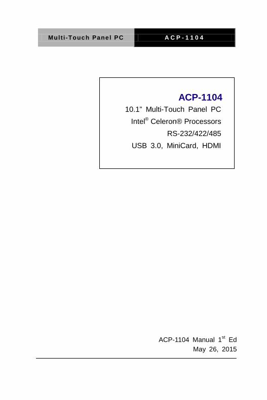
Mult i -Touch Panel PC A C P - 1 1 0 4
ACP-1104
10.1” Multi-Touch Panel PC Intel® Celeron® Processors
RS-232/422/485 USB 3.0, MiniCard, HDMI
ACP-1104 Manual 1st Ed May 26, 2015
Mult i -Touch Panel PC A C P - 1 1 0 4
Copyright Notice
This document is copyrighted, 2015. All rights are reserved. The original manufacturer reserves the right to make improvements to the products described in this manual at any time without notice.
No part of this manual may be reproduced, copied, translated, or transmitted in any form or by any means without the prior written permission of the original manufacturer. Information provided in this manual is intended to be accurate and reliable. However, the original manufacturer assumes no responsibility for its use, nor for any infringements upon the rights of third parties, which may result from its use.
The material in this document is for product information only and is subject to change without notice. While reasonable efforts have been made in the preparation of this document to assure its accuracy, AAEON, assumes no liabilities resulting from errors or omissions in this document, or from the use of the information contained herein.
AAEON reserves the right to make changes in the product design without notice to its users.
i

Mult i -Touch Panel PC A C P - 1 1 0 4
Acknowledgments
Intel®, AtomTM are registered trademarks of Intel® Corporation.
Microsoft® Windows is a registered trademark of Microsoft®
Corporation.
RTL is a trademark of Realtek Semi-Conductor Co., Ltd.
C&T is a trademark of Chips and Technologies, Inc.
UMC is a trademark of United Microelectronics Corporation.
ITE is a trademark of Integrated Technology Express, Inc.
All other product names or trademarks are properties of their respective owners.
ii
Mult i -Touch Panel PC A C P - 1 1 0 4
Packing List
Before you begin installing your Panel PC, please make sure that the
following items have been shipped:
ACP-1104 Multi-Touch Panel PC
RJ-45 COM Port Cable x 2
Power Adapter x 1
Product DVD with User’s Manual (in pdf), drivers and
utilities
VESA Mount
Panel Mount
If any of these items are missing or damaged, you should contact your
distributor or sales representative immediately.
iii
Mult i -Touch Panel PC A C P - 1 1 0 4
Safety & Warranty
Please read the following safety instructions carefully. It is advised
that you keep this manual for future references
1. Disconnect this device from any AC supply before cleaning.
2. While cleaning, use a damp cloth instead of liquid or spray
detergents.
3. For any pluggable equipment, the power outlet must be installed
near the device and easily accessible.
4. Keep this device away from humidity.
5. Place this device on a solid surface during installation. Dropping
it or letting it fall could cause damage.
6. The openings on the device’s enclosure are for dissipating heat.
DO NOT COVER THE OPENINGS.
7. Watch out for high temperatures that may occur during system
operation.
8. Make sure the voltage of the power source is correct before
connecting the device to the power outlet.
9. Position the power cord so that people cannot step on it. Do not
place anything over the power cord.
10. All cautions and warnings on the device should be noted.
11. If the device is not to be used for a long time, disconnect it from
the power supply to avoid damage by transient over-voltage.
12. Never pour any liquid into the openings. This could cause fire or
electric shock.
13. As most electronic components are sensitive to static electrical
iv
Mult i -Touch Panel PC A C P - 1 1 0 4
charge, be sure to ground yourself to prevent static charge when
installing the internal components. Use a grounding wrist strap
and contain all electronic components in any static-shielded
devices.
14. If any of the following situations arises, please the contact
our service personnel:
i. Damaged power cord or plug
ii. Liquid intrusion to the device
iii. Exposure to moisture
iv. Device is not working as expected or in a manner
as described in this manual
v. The device is dropped or damaged
vi. Any obvious signs of damage displayed on the
device
15. DO NOT LEAVE THIS DEVICE IN AN UNCONTROLLED
ENVIRONMENT WHERE THE STORAGE TEMPERATURE IS
BELOW -10° C (14°F) OR ABOVE 60° C (140° F) TO
PREVENT DAMAGE. 16. External equipment intended for connection to signal input/output
or other connectors, shall comply with relevant UL / IEC standard (e.g. UL 1950 for IT equipment and UL 60601-1 / IEC 60601 series for systems – shall comply with the standard IEC 60601-1-1, Safety requirements for medical electrical systems. Equipment not complying with UL 60601-1 shall be kept outside the patient environment, as defined in the standard.
17. When the temperature of CPU is higher than 35°C, the frequency
of CPU will be adjusted automatically. For example, if the
v
Mult i -Touch Panel PC A C P - 1 1 0 4
temperature of Intel Core i7 is 40°C, the frequency of the CPU will be between 1.8~1.3 GHz.
FCC This device complies with Part 15 FCC Rules.
Operation is subject to the following two
conditions: (1) this device may not cause
harmful interference, and (2) this device must
accept any interference received including
interference that may cause undesired
operation.
Caution: There is a danger of explosion if the battery is incorrectly replaced.
Replace only with the same or equivalent type recommended by the
manufacturer. Dispose of used batteries according to the
manufacturer’s instructions and your local government’s recycling or
disposal directives.
vi

Mult i -Touch Panel PC A C P - 1 1 0 4
Classification
1. Degree of production against electric shock: not classified
2. Degree of protection against the ingress of water: IPX1
3. Equipment not suitable for use in the presence of a flammable
anesthetic mixture with air or with oxygen or nitrous oxide.
4. Mode of operation: Continuous
5. Type of protection against electric shock: Class I equipment
vii
Mult i -Touch Panel PC A C P - 1 1 0 4
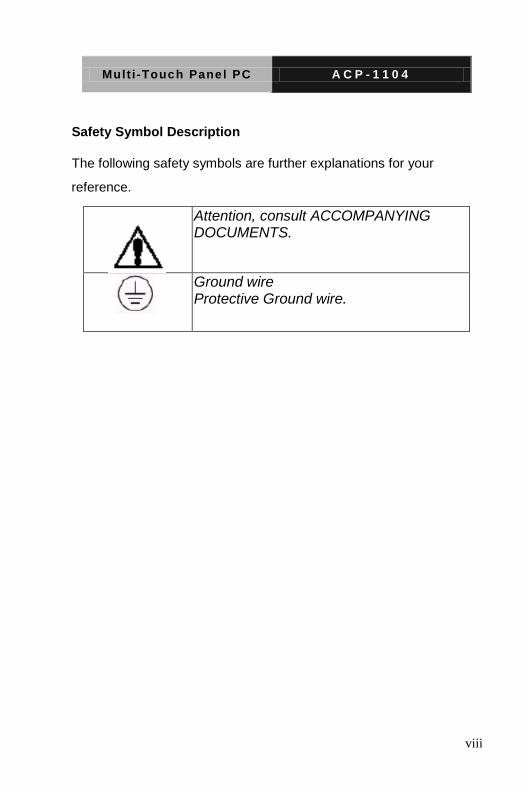
Safety Symbol Description
The following safety symbols are further explanations for your
reference.
Attention, consult ACCOMPANYING DOCUMENTS.
Ground wire Protective Ground wire.
viii
Mult i -Touch Panel PC A C P - 1 1 0 4
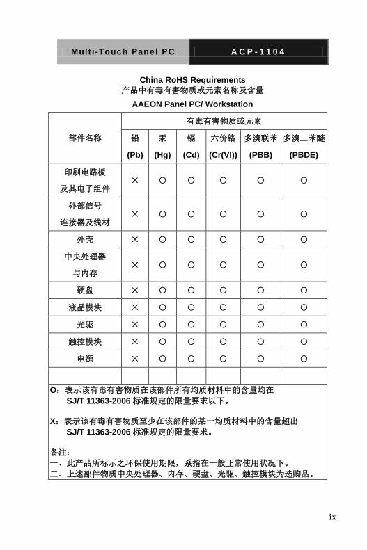
China RoHS Requirements
产品中有毒有害物质或元素名称及含量 AAEON Panel PC/ Workstation
部件名称
有毒有害物质或元素
铅
(Pb)
汞
(Hg)
镉
(Cd)
六价铬
(Cr(VI))
多溴联苯
(PBB)
多溴二苯醚
(PBDE)
印刷电路板
及其电子组件 × ○ ○ ○ ○ ○
外部信号
连接器及线材 × ○ ○ ○ ○ ○
外壳 × ○ ○ ○ ○ ○
中央处理器
与内存 × ○ ○ ○ ○ ○
硬盘 × ○ ○ ○ ○ ○
液晶模块 × ○ ○ ○ ○ ○
光驱 × ○ ○ ○ ○ ○
触控模块 × ○ ○ ○ ○ ○
电源 × ○ ○ ○ ○ ○
O:表示该有毒有害物质在该部件所有均质材料中的含量均在
SJ/T 11363-2006 标准规定的限量要求以下。 X:表示该有毒有害物质至少在该部件的某一均质材料中的含量超出
SJ/T 11363-2006 标准规定的限量要求。 备注: 一、此产品所标示之环保使用期限,系指在一般正常使用状况下。 二、上述部件物质中央处理器、内存、硬盘、光驱、触控模块为选购品。
ix
Mult i -Touch Panel PC A C P - 1 1 0 4
Contents
Chapter 1 General Information
1.1 Introduction ................................................................ 1-2
1.2 Features .................................................................... 1-3
1.3 Specification .............................................................. 1-4
Chapter 2 Hardware Installation
2.1 Safety Precautions .................................................... 2-2
2.2 Mechanical Drawings ................................................ 2-3
2.3 List of Jumpers .......................................................... 2-5
2.4 List of Connectors ..................................................... 2-6
2.5 AT/ATX Mode Selection (JP1) .................................. 2-7
2.6 LVDS BKLT Control Selection (JP2) ......................... 2-7
2.7 LVDS Power Selection (JP3) .................................... 2-7
2.8 LVDS BKLT Power Selection (JP4) .......................... 2-8
2.9 Clear CMOS Jumper (JP5) ....................................... 2-8
2.10 Dry and Wet Contact Digital Input Power Selection
(JP6) ................................................................................ 2-8
2.11 Dry and Wet Contact Digital Output Power Selection
(JP7) ................................................................................ 2-9
2.12 HDMI Display (CN1) ................................................ 2-9
2.13 USB 3.0 Connector (CN2) ....................................... 2-10
2.14 COM2 RS-232/422/485 Connector (CN4) .............. 2-11
2.15 COM3 RS-232 I/F (CN16) ....................................... 2-11
x
Mult i -Touch Panel PC A C P - 1 1 0 4
2.16 COM1 RS-232/422/485 Connector (CN17) ............ 2-12
2.17 Dry and Wet Contact Digital Input (CN23) .............. 2-13
2.18 Dry and Wet Contact Digital Output (CN24) ........... 2-15
2.19 RJ-45 Ethernet Port (CN26) .................................... 2-16
2.20 RJ-45 Ethernet Port (CN27) .................................... 2-16
2.21 USB 2.0 Port 1 Connector (USB1) .......................... 2-17
2.22 USB 2.0 Port 2 Connector (USB2) .......................... 2-17
2.23 USB 2.0 Port 3 Connector (USB3) .......................... 2-18
2.24 DDR3L SODIMM Slot (DIMM1) .............................. 2-18
2.25 Half Size MiniCard Slot (PCIE1) ............................. 2-18
2.26 PCI-E Full Size MiniCard Slot (PCIE2) ................... 2-20
2.27 COM-to-RJ-45 Converter Cable (For COM1 &
COM2) ............................................................................. 2-23
2.28 Mounting the Panel ................................................. 2-24
Chapter 3 AMI BIOS Setup
3.1 System Test and Initialization. .................................. 3-2
3.2 AMI BIOS Setup ........................................................ 3-3
Chapter 4 Driver Installation
4.1 Installation ................................................................. 4-3
Appendix A Programming The Watchdog Timer
A.1 Watchdog Timer Initial Program ............................ A-2
Appendix B I/O Information
B.1 I/O Address Map .................................................. B-2
xi
Mult i -Touch Panel PC A C P - 1 1 0 4
B.2 Memory Address Map .......................................... B-4
B.3 IRQ Mapping Chart .............................................. B-5
Appendix C Electrical Specifications for I/O Ports
C.1 Electrical Specifications for I/O Ports .................. C-2
C.2 DIO Programming ............................................... C-3
C.3 Digital I/O Register .............................................. C-4
C.4 Digital I/O Sample Program ................................ C-5
xii
Mult i -Touch Panel PC A C P - 1 1 0 4
General Information
Chapter
1
Chapter 1 General Information 1-1
Mult i -Touch Panel PC A C P - 1 1 0 4
1.1 Introduction
This User’s Manual contains all the essential information regarding
the ACP-1104. It provides detailed descriptions and explanations
on the product’s hardware and software features, such as its
specifications, dimensions, jumper/connector settings/definitions,
and driver installation instructions, to facilitate users in setting up
their product.
User may refer to the AAEON.com for the latest version of this
document.
Chapter 1 General Information 1-2
Mult i -Touch Panel PC A C P - 1 1 0 4
1.2 Features
10.1” Multi-Touch screen
Aluminum Design
7H Two-point Multi-Touch Display
Intel® Celeron® J1900/ N2807 Processor
Supports VESA 75 Mounting Interface
Chapter 1 General Information 1-3
Mult i -Touch Panel PC A C P - 1 1 0 4
1.3 Specification
System
Processor Intel® Atom™ J1900/N2807 Processor
System Memory 204-pin DDR3L 1333 SODIMM x 1, Up
to 8 GB (Pre-installed 2 GB)
LCD / CRT Controller LVDS
I/O Port USB 3.0 x 1
USB 2.0 x 3
LAN x 2
DIO x 6 (DI x 4, DO x 2, w/o isolation)
RJ-45 x 2 for RS-232/422/485 (BIOS
Selection)
HDMI x 1
Antenna Hole x 2
Power Button x 1
Lockable Power Connector x 1
Storage Device mSATA (half-size) x 1
Expansion MiniCard (Full-size) x 1 (mSATA only),
MiniCard (Half-size) x 1
OS Support Windows® Embedded Standard 8
32/64-bit,
Windows® Embedded Standard 7
32/64-bit,
Windows® 8.1 32/64-bit
Chapter 1 General Information 1-4
Mult i -Touch Panel PC A C P - 1 1 0 4
Windows® 7 32/64-bit
Linux by Fedora kernel 2.6.3 up
Mechanical
Construction IP65/ NEMA4-rated Aluminum Front
Bezel
Mounting VESA 75
Panel Mount
Dimension 266 x 183.5 x 30mm
Carton Dimension 345 x 200 x 245mm
Net Weight 1.2 kg
Gross Weight 2.5 kg
Environmental
Operating Temperature 32°F ~ 113°F (0°C ~ 45°C) ( mSATA/
J1900 ) - without airflow
32°F ~ 122°F (0°C ~ 50°C) ( mSATA/
J1900 ) - with airflow
Storage Temperature 5 ~ 95% @ 40oC, non-condensing
Storage Humidity 10 ~ 90% @ 40oC, non-condensing
Anti-Vibration 3 Grms/ 5~500 Hz/ operation (mSATA)
Anti-Shock 20 G peak acceleration (11 msec.
duration, mSATA)
EMC CE/FCC Class A
Power Supply
DC Input DC 12 V
Chapter 1 General Information 1-5
Mult i -Touch Panel PC A C P - 1 1 0 4
LCD
Display Type
Max. Resolution
Max. Colors
Luminance (cd/m2)
Contrast Ratio
Viewing Angle
10.1”, WXGA, LED
1280 x 800
262 K
250 nits
600:1
80º (H), 70º (V)
Touchscreen
Type USB
Resolution 2048 x 2048
Light Transmission >86%
Chapter 1 General Information 1-6

Mult i -Touch Panel PC A C P - 1 1 0 4
Chapter 2 Hardware Installation 2-1
Hardware Installation
Chapter
2
Mult i -Touch Panel PC A C P - 1 1 0 4
Chapter 2 Hardware Installation 2-2
2.1 Safety Precautions
Always completely disconnect the power cord from your board whenever you are working on it. Do not make connections while the power is on, because a sudden rush of power can damage sensitive electronic components.
Always ground yourself to remove any static charge before touching the board. Modern electronic devices are very sensitive to static electric charges. Use a grounding wrist strap at all times. Place all electronic components on a static-dissipative surface or in a static-shielded bag when they are not in the chassis
Mult i -Touch Panel PC A C P - 1 1 0 4
Chapter 2 Hardware Installation 2-3
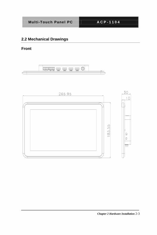
2.2 Mechanical Drawings
Front
Mult i -Touch Panel PC A C P - 1 1 0 4
Chapter 2 Hardware Installation 2-4
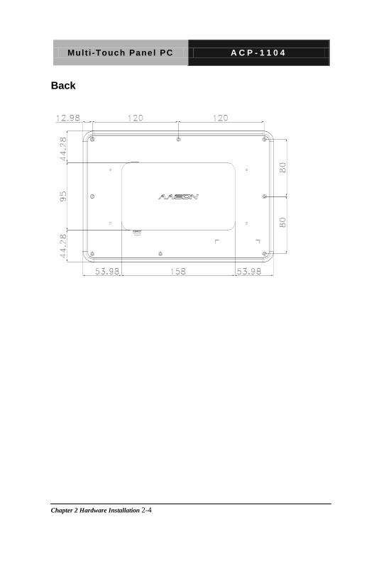
Back
Mult i -Touch Panel PC A C P - 1 1 0 4
Chapter 2 Hardware Installation 2-5
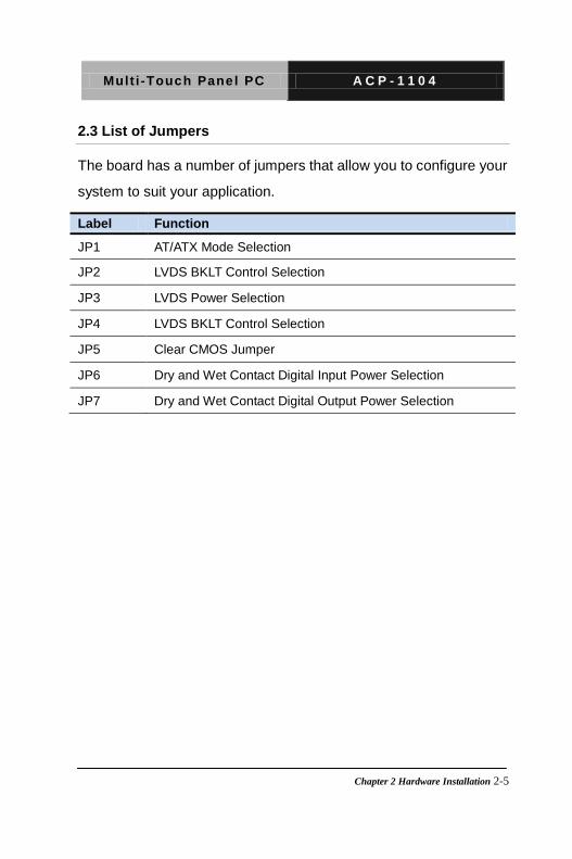
2.3 List of Jumpers
The board has a number of jumpers that allow you to configure your
system to suit your application.
Label Function
JP1 AT/ATX Mode Selection
JP2 LVDS BKLT Control Selection
JP3 LVDS Power Selection
JP4 LVDS BKLT Control Selection
JP5 Clear CMOS Jumper
JP6 Dry and Wet Contact Digital Input Power Selection
JP7 Dry and Wet Contact Digital Output Power Selection
Mult i -Touch Panel PC A C P - 1 1 0 4
Chapter 2 Hardware Installation 2-6
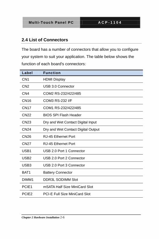
2.4 List of Connectors
The board has a number of connectors that allow you to configure
your system to suit your application. The table below shows the
function of each board's connectors:
Label Function
CN1 HDMI Display
CN2 USB 3.0 Connector
CN4 COM2 RS-232/422/485
CN16 COM3 RS-232 I/F
CN17 COM1 RS-232/422/485
CN22 BIOS SPI Flash Header
CN23 Dry and Wet Contact Digital Input
CN24 Dry and Wet Contact Digital Output
CN26 RJ-45 Ethernet Port
CN27 RJ-45 Ethernet Port
USB1 USB 2.0 Port 1 Connector
USB2 USB 2.0 Port 2 Connector
USB3 USB 2.0 Port 3 Connector
BAT1 Battery Connector
DIMM1 DDR3L SODIMM Slot
PCIE1 mSATA Half Size MiniCard Slot
PCIE2 PCI-E Full Size MiniCard Slot
Mult i -Touch Panel PC A C P - 1 1 0 4
Chapter 2 Hardware Installation 2-7
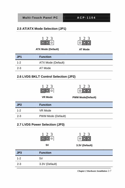
2.5 AT/ATX Mode Selection (JP1)
1 2 3
ATX Mode (Default)
1 2 3
AT Mode
JP1 Function
1-2 ATX Mode (Default)
2-3 AT Mode
2.6 LVDS BKLT Control Selection (JP2)
1 2 3
VR Mode
1 2 3
PWM Mode(Default)
JP2 Function
1-2 VR Mode
2-3 PWM Mode (Default)
2.7 LVDS Power Selection (JP3)
1 2 3
5V
1 2 3
3.3V (Default)
JP3 Function
1-2 5V
2-3 3.3V (Default)
Mult i -Touch Panel PC A C P - 1 1 0 4
Chapter 2 Hardware Installation 2-8
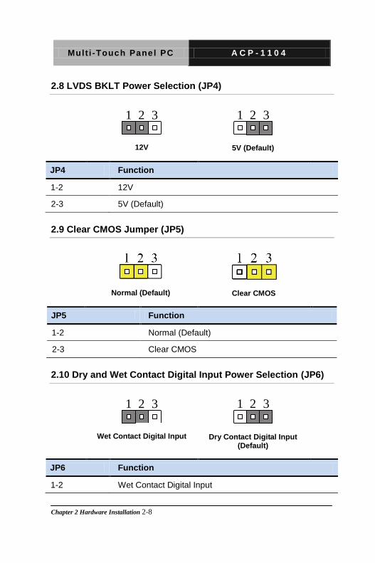
2.8 LVDS BKLT Power Selection (JP4)
1 2 3
12V
1 2 3
5V (Default)
JP4 Function
1-2 12V
2-3 5V (Default)
2.9 Clear CMOS Jumper (JP5)
Normal (Default)
Clear CMOS
JP5 Function
1-2 Normal (Default)
2-3 Clear CMOS
2.10 Dry and Wet Contact Digital Input Power Selection (JP6)
1 2 3
Wet Contact Digital Input
1 2 3
Dry Contact Digital Input (Default)
JP6 Function
1-2 Wet Contact Digital Input
Mult i -Touch Panel PC A C P - 1 1 0 4
Chapter 2 Hardware Installation 2-9
2-3 Dry Contact Digital Input (Default)
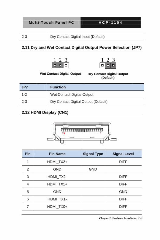
2.11 Dry and Wet Contact Digital Output Power Selection (JP7)
1 2 3
Wet Contact Digital Output
1 2 3
Dry Contact Digital Output (Default)
JP7 Function
1-2 Wet Contact Digital Output
2-3 Dry Contact Digital Output (Default)
2.12 HDMI Display (CN1)
Pin Pin Name Signal Type Signal Level
1 HDMI_TX2+ DIFF
2 GND GND
3 HDMI_TX2- DIFF
4 HDMI_TX1+ DIFF
5 GND GND
6 HDMI_TX1- DIFF
7 HDMI_TX0+ DIFF
Mult i -Touch Panel PC A C P - 1 1 0 4
Chapter 2 Hardware Installation 2-10
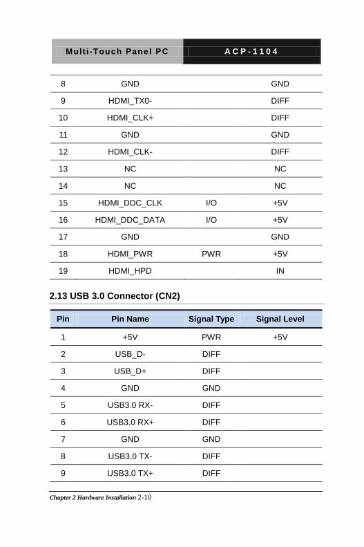
8 GND GND
9 HDMI_TX0- DIFF
10 HDMI_CLK+ DIFF
11 GND GND
12 HDMI_CLK- DIFF
13 NC NC
14 NC NC
15 HDMI_DDC_CLK I/O +5V
16 HDMI_DDC_DATA I/O +5V
17 GND GND
18 HDMI_PWR PWR +5V
19 HDMI_HPD IN
2.13 USB 3.0 Connector (CN2)
Pin Pin Name Signal Type Signal Level
1 +5V PWR +5V
2 USB_D- DIFF
3 USB_D+ DIFF
4 GND GND
5 USB3.0 RX- DIFF
6 USB3.0 RX+ DIFF
7 GND GND
8 USB3.0 TX- DIFF
9 USB3.0 TX+ DIFF
Mult i -Touch Panel PC A C P - 1 1 0 4
Chapter 2 Hardware Installation 2-11
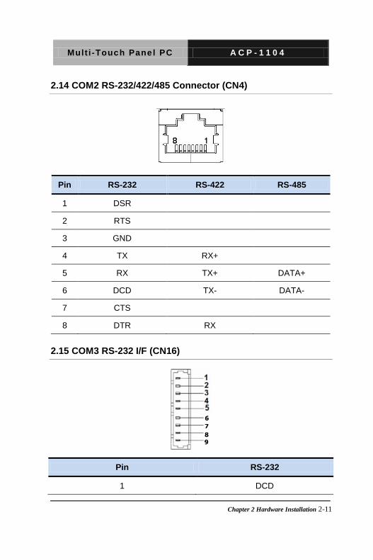
2.14 COM2 RS-232/422/485 Connector (CN4)
Pin RS-232 RS-422 RS-485
1 DSR
2 RTS
3 GND
4 TX RX+
5 RX TX+ DATA+
6 DCD TX- DATA-
7 CTS
8 DTR RX
2.15 COM3 RS-232 I/F (CN16)
Pin RS-232
1 DCD
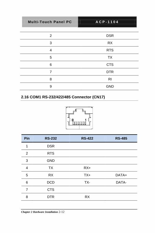
Mult i -Touch Panel PC A C P - 1 1 0 4
Chapter 2 Hardware Installation 2-12
2 DSR
3 RX
4 RTS
5 TX
6 CTS
7 DTR
8 RI
9 GND
2.16 COM1 RS-232/422/485 Connector (CN17)
Pin RS-232 RS-422 RS-485
1 DSR
2 RTS
3 GND
4 TX RX+
5 RX TX+ DATA+
6 DCD TX- DATA-
7 CTS
8 DTR RX
Mult i -Touch Panel PC A C P - 1 1 0 4
Chapter 2 Hardware Installation 2-13
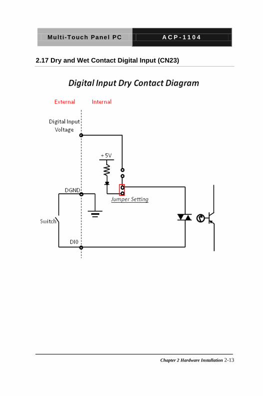
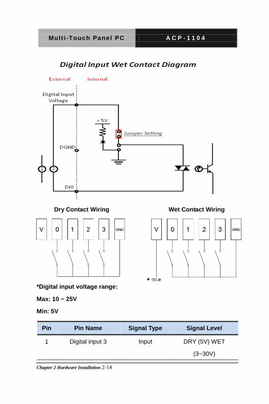
2.17 Dry and Wet Contact Digital Input (CN23)
Mult i -Touch Panel PC A C P - 1 1 0 4
Chapter 2 Hardware Installation 2-14
*Digital input voltage range:
Max: 10 ~ 25V
Min: 5V
Pin Pin Name Signal Type Signal Level
1 Digital input 3 Input DRY (5V) WET
(3~30V)
*
Wet Contact Wiring Dry Contact Wiring
Mult i -Touch Panel PC A C P - 1 1 0 4
Chapter 2 Hardware Installation 2-15
2 Digital input 2 Input DRY (5V) WET
(3~30V)
3 Digital input 1 Input DRY (5V) WET
(3~30V)
4 Digital input 0 Input DRY (5V) WET
(3~30V)
5 WET contact POWER PWR 3~30V
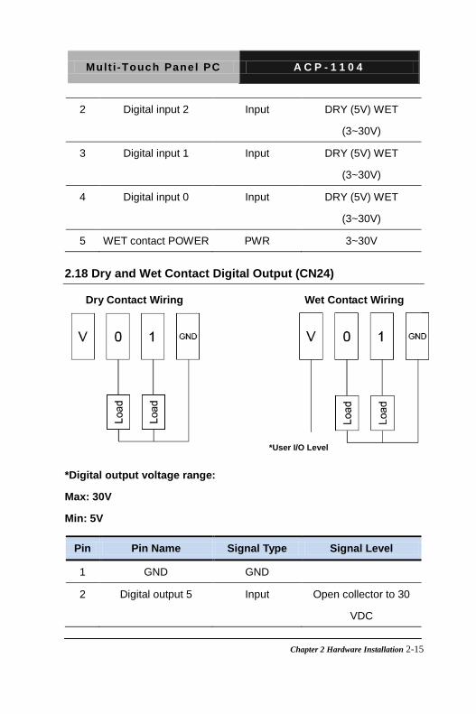
2.18 Dry and Wet Contact Digital Output (CN24)
*Digital output voltage range:
Max: 30V
Min: 5V
Pin Pin Name Signal Type Signal Level
1 GND GND
2 Digital output 5 Input Open collector to 30
VDC
Dry Contact Wiring Wet Contact Wiring
*User I/O Level
Mult i -Touch Panel PC A C P - 1 1 0 4
Chapter 2 Hardware Installation 2-16
3 Digital output 4 Input Open collector to 30
VDC
4 Digital output POWER Input 3 ~ 30 V
5 GND GND
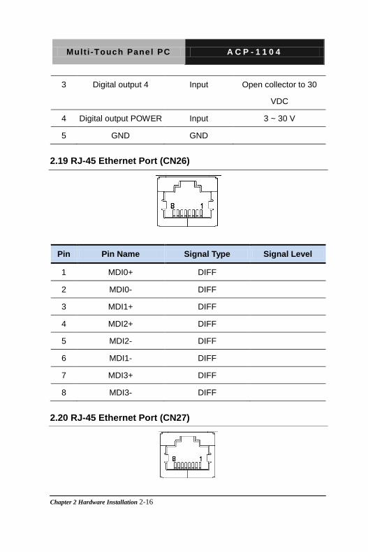
2.19 RJ-45 Ethernet Port (CN26)
Pin Pin Name Signal Type Signal Level
1 MDI0+ DIFF
2 MDI0- DIFF
3 MDI1+ DIFF
4 MDI2+ DIFF
5 MDI2- DIFF
6 MDI1- DIFF
7 MDI3+ DIFF
8 MDI3- DIFF
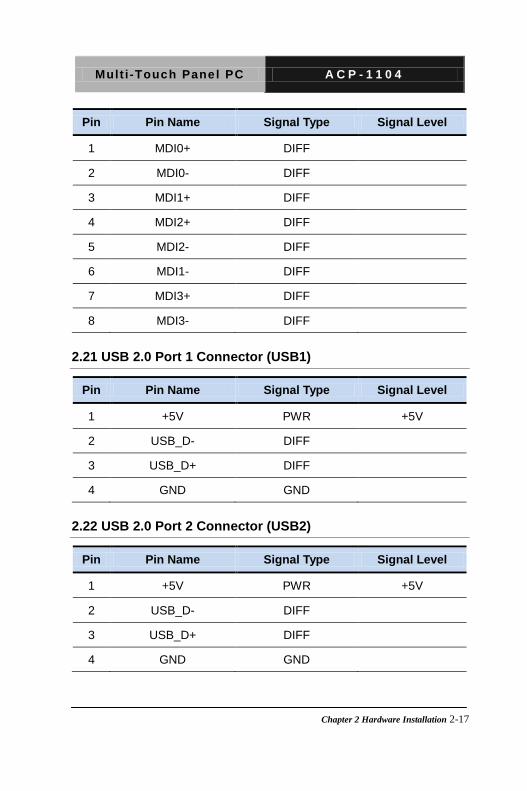
2.20 RJ-45 Ethernet Port (CN27)
Mult i -Touch Panel PC A C P - 1 1 0 4
Chapter 2 Hardware Installation 2-17
Pin Pin Name Signal Type Signal Level
1 MDI0+ DIFF
2 MDI0- DIFF
3 MDI1+ DIFF
4 MDI2+ DIFF
5 MDI2- DIFF
6 MDI1- DIFF
7 MDI3+ DIFF
8 MDI3- DIFF
2.21 USB 2.0 Port 1 Connector (USB1)
Pin Pin Name Signal Type Signal Level
1 +5V PWR +5V
2 USB_D- DIFF
3 USB_D+ DIFF
4 GND GND
2.22 USB 2.0 Port 2 Connector (USB2)
Pin Pin Name Signal Type Signal Level
1 +5V PWR +5V
2 USB_D- DIFF
3 USB_D+ DIFF
4 GND GND
Mult i -Touch Panel PC A C P - 1 1 0 4
Chapter 2 Hardware Installation 2-18
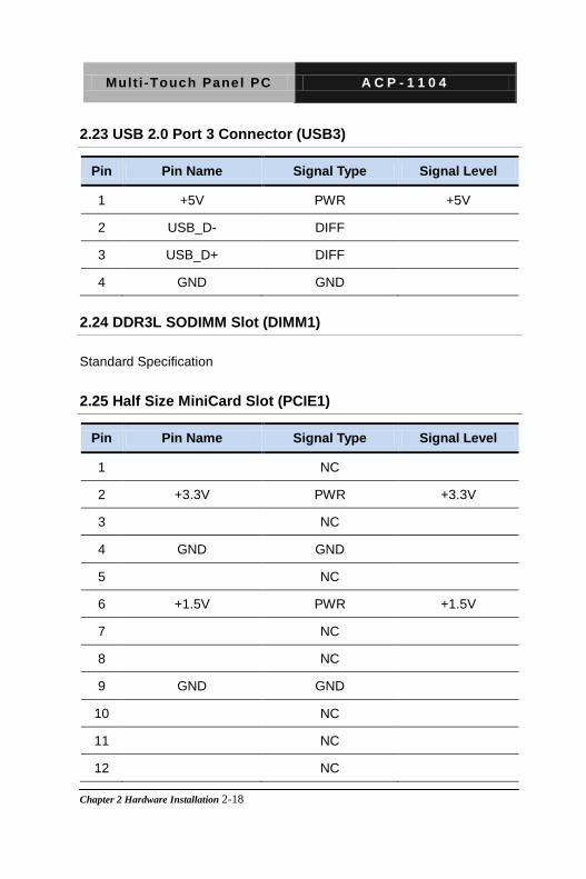
2.23 USB 2.0 Port 3 Connector (USB3)
Pin Pin Name Signal Type Signal Level
1 +5V PWR +5V
2 USB_D- DIFF
3 USB_D+ DIFF
4 GND GND
2.24 DDR3L SODIMM Slot (DIMM1)
Standard Specification
2.25 Half Size MiniCard Slot (PCIE1)
Pin Pin Name Signal Type Signal Level
1 NC
2 +3.3V PWR +3.3V
3 NC
4 GND GND
5 NC
6 +1.5V PWR +1.5V
7 NC
8 NC
9 GND GND
10 NC
11 NC
12 NC
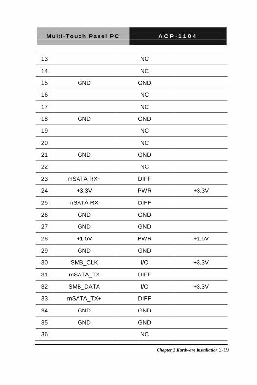
Mult i -Touch Panel PC A C P - 1 1 0 4
Chapter 2 Hardware Installation 2-19
13 NC
14 NC
15 GND GND
16 NC
17 NC
18 GND GND
19 NC
20 NC
21 GND GND
22 NC
23 mSATA RX+ DIFF
24 +3.3V PWR +3.3V
25 mSATA RX- DIFF
26 GND GND
27 GND GND
28 +1.5V PWR +1.5V
29 GND GND
30 SMB_CLK I/O +3.3V
31 mSATA_TX DIFF
32 SMB_DATA I/O +3.3V
33 mSATA_TX+ DIFF
34 GND GND
35 GND GND
36 NC
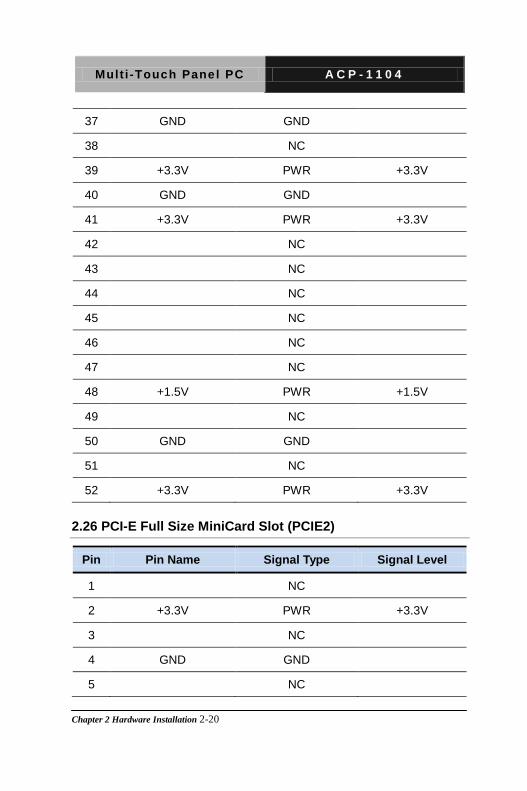
Mult i -Touch Panel PC A C P - 1 1 0 4
Chapter 2 Hardware Installation 2-20
37 GND GND
38 NC
39 +3.3V PWR +3.3V
40 GND GND
41 +3.3V PWR +3.3V
42 NC
43 NC
44 NC
45 NC
46 NC
47 NC
48 +1.5V PWR +1.5V
49 NC
50 GND GND
51 NC
52 +3.3V PWR +3.3V
2.26 PCI-E Full Size MiniCard Slot (PCIE2)
Pin Pin Name Signal Type Signal Level
1 NC
2 +3.3V PWR +3.3V
3 NC
4 GND GND
5 NC
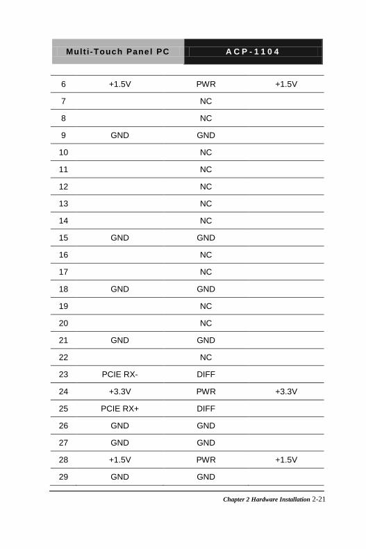
Mult i -Touch Panel PC A C P - 1 1 0 4
Chapter 2 Hardware Installation 2-21
6 +1.5V PWR +1.5V
7 NC
8 NC
9 GND GND
10 NC
11 NC
12 NC
13 NC
14 NC
15 GND GND
16 NC
17 NC
18 GND GND
19 NC
20 NC
21 GND GND
22 NC
23 PCIE RX- DIFF
24 +3.3V PWR +3.3V
25 PCIE RX+ DIFF
26 GND GND
27 GND GND
28 +1.5V PWR +1.5V
29 GND GND
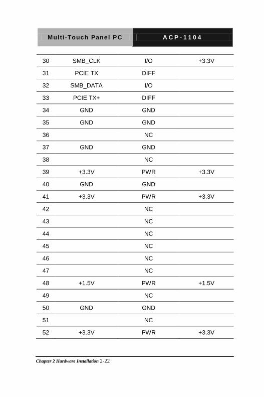
Mult i -Touch Panel PC A C P - 1 1 0 4
Chapter 2 Hardware Installation 2-22
30 SMB_CLK I/O +3.3V
31 PCIE TX DIFF
32 SMB_DATA I/O
33 PCIE TX+ DIFF
34 GND GND
35 GND GND
36 NC
37 GND GND
38 NC
39 +3.3V PWR +3.3V
40 GND GND
41 +3.3V PWR +3.3V
42 NC
43 NC
44 NC
45 NC
46 NC
47 NC
48 +1.5V PWR +1.5V
49 NC
50 GND GND
51 NC
52 +3.3V PWR +3.3V
Mult i -Touch Panel PC A C P - 1 1 0 4
Chapter 2 Hardware Installation 2-23
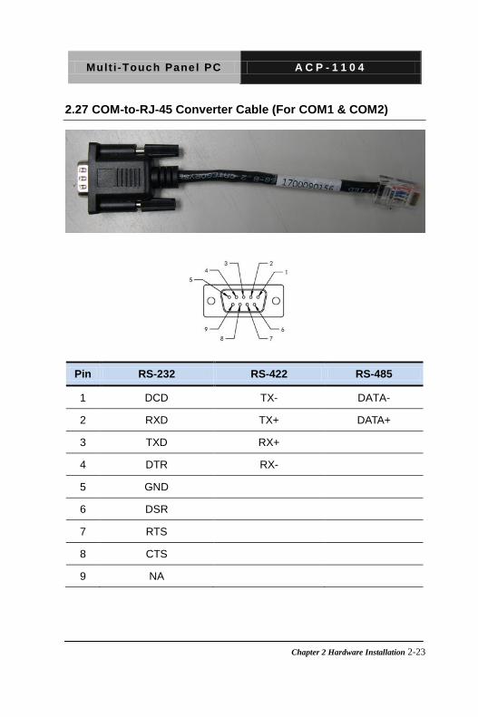
2.27 COM-to-RJ-45 Converter Cable (For COM1 & COM2)
Pin RS-232 RS-422 RS-485
1 DCD TX- DATA-
2 RXD TX+ DATA+
3 TXD RX+
4 DTR RX-
5 GND
6 DSR
7 RTS
8 CTS
9 NA
Mult i -Touch Panel PC A C P - 1 1 0 4
Chapter 2 Hardware Installation 2-24
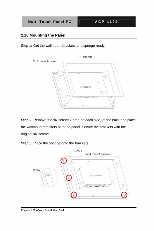
2.28 Mounting the Panel
Step 1: Get the wallmount brackets and sponge ready.
Wall mount bracket
Sponge
Step 2: Remove the six screws (three on each side) at the back and place
the wallmount brackets onto the panel. Secure the brackets with the
original six screws.
Step 3: Place the sponge onto the brackets
1
3-screw
Sponge
Wall mount bracket
Mult i -Touch Panel PC A C P - 1 1 0 4
Chapter 2 Hardware Installation 2-25
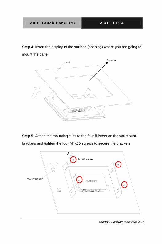
Step 4: Insert the display to the surface (opening) where you are going to
mount the panel
2 wall
Step 5: Attach the mounting clips to the four fillisters on the wallmount
brackets and tighten the four M4x60 screws to secure the brackets
3
4-mounting clip
1
2
Opening
M4x60 screw
Mult i -Touch Panel PC A C P - 1 1 0 4
AMI BIOS Setup
Chapter
3
Chapter 3 AMI BIOS Setup 3-1
Mult i -Touch Panel PC A C P - 1 1 0 4
3.1 System Test and Iinitialization
These routines test and initialize board hardware. If the routines
encounter an error during the tests, you will either hear a few short
beeps or see an error message on the screen. There are two kinds
of errors: fatal and non-fatal. The system can usually continue the
boot up sequence with non-fatal errors.
System configuration verification
These routines check the current system configuration stored in the
CMOS memory and BIOS NVRAM. If system configuration is not
found or system configuration data error is detected, system will
load optimized default and re-boot with this default system
configuration automatically.
There are four situations in which you will need to setup system
configuration:
1. You are starting your system for the first time
2. You have changed the hardware attached to your system
3. The system configuration is reset by Clear-CMOS jumper
4. The CMOS memory has lost power and the configuration
information has been erased.
The ACP-1104 CMOS memory has an integral lithium battery
backup for data retention. However, you will need to replace the
complete unit when it depletes.
Chapter 3 AMI BIOS Setup 3-2
Mult i -Touch Panel PC A C P - 1 1 0 4
3.2 AMI BIOS Setup
AMI BIOS ROM has a built-in Setup program that allows users to
modify the basic system configuration. This type of information is
stored in battery-backed CMOS RAM and BIOS NVRAM so that it
retains the Setup information when the power is turned off.
Entering Setup
Power on the computer and press <Del> immediately. This will
allow you to enter Setup.
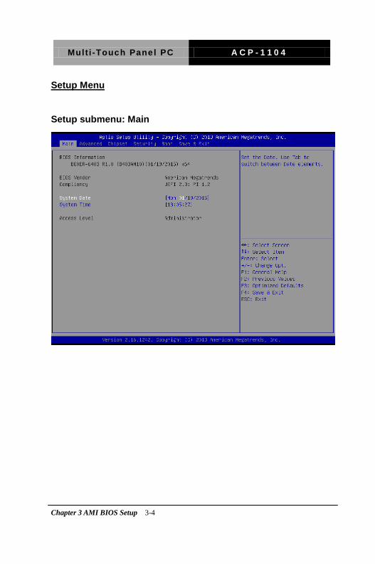
Main
Set the date, use tab to switch between date elements.
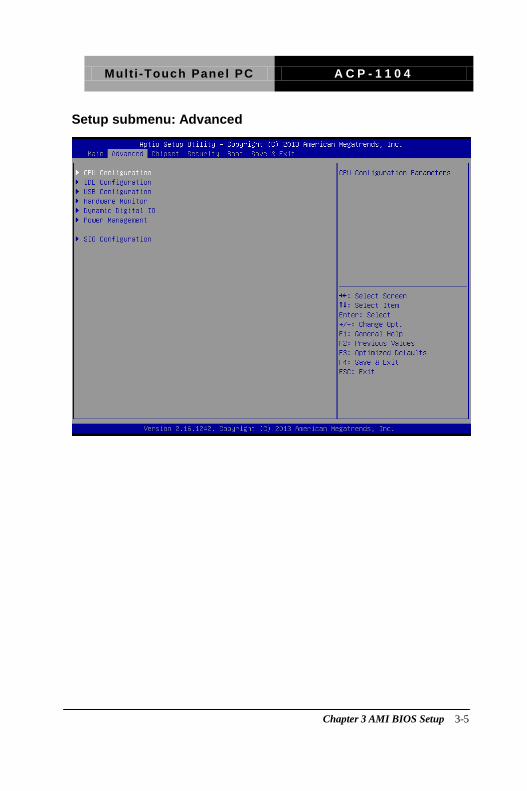
Advanced
Enable disable boot option for legacy network devices.
Chipset
Host bridge parameters.
Boot
Enables/disable quiet boot option.
Security
Set setup administrator password.
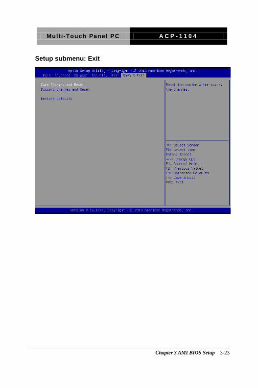
Save & Exit
Exit system setup after saving the changes.
Chapter 3 AMI BIOS Setup 3-3
Mult i -Touch Panel PC A C P - 1 1 0 4
Setup Menu
Setup submenu: Main
Chapter 3 AMI BIOS Setup 3-4
Mult i -Touch Panel PC A C P - 1 1 0 4
Setup submenu: Advanced
Chapter 3 AMI BIOS Setup 3-5
Mult i -Touch Panel PC A C P - 1 1 0 4
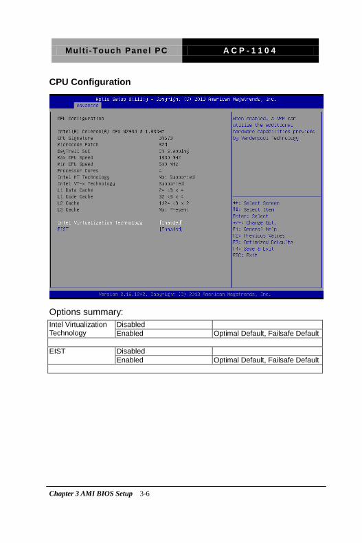
CPU Configuration
Options summary: Intel Virtualization Technology
Disabled Enabled Optimal Default, Failsafe Default
EIST Disabled
Enabled Optimal Default, Failsafe Default
Chapter 3 AMI BIOS Setup 3-6

Mult i -Touch Panel PC A C P - 1 1 0 4
IDE Configuration (IDE)
Options summary: SATA Mode IDE Mode
AHCI Mode Optimal Default, Failsafe Default
Chapter 3 AMI BIOS Setup 3-7
Mult i -Touch Panel PC A C P - 1 1 0 4
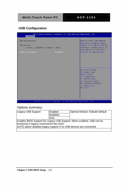
USB Configuration
Options summary: Legacy USB Support Enabled Optimal Default, Failsafe Default
Disabled Auto
Enables BIOS Support for Legacy USB Support. When enabled, USB can be functional in legacy environment like DOS. AUTO option disables legacy support if no USB devices are connected
Chapter 3 AMI BIOS Setup 3-8
Mult i -Touch Panel PC A C P - 1 1 0 4
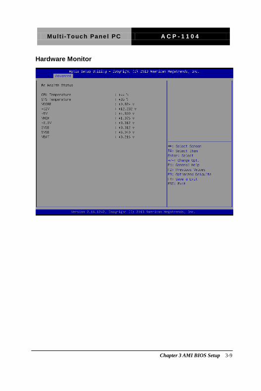
Hardware Monitor
Chapter 3 AMI BIOS Setup 3-9
Mult i -Touch Panel PC A C P - 1 1 0 4
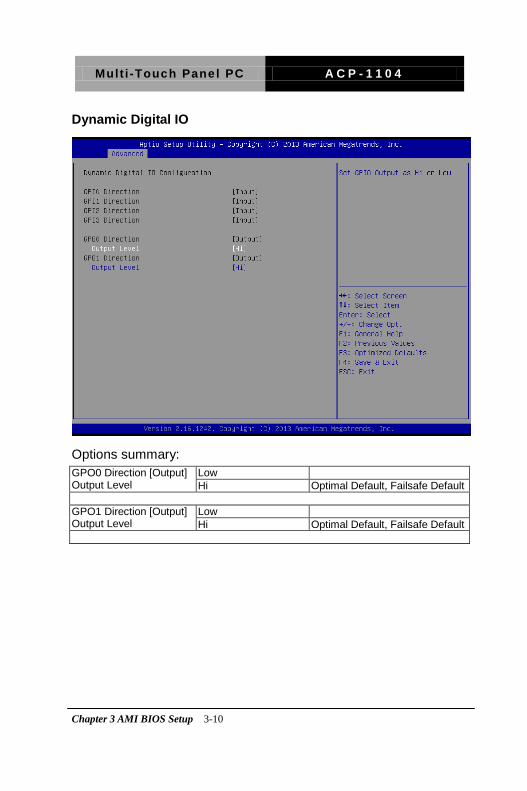
Dynamic Digital IO
Options summary: GPO0 Direction [Output] Output Level
Low Hi Optimal Default, Failsafe Default
GPO1 Direction [Output] Output Level
Low Hi Optimal Default, Failsafe Default
Chapter 3 AMI BIOS Setup 3-10
Mult i -Touch Panel PC A C P - 1 1 0 4
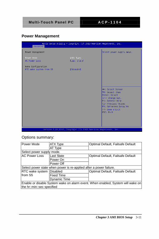
Power Management
Options summary:
Power Mode ATX Type Optimal Default, Failsafe Default AT Type
Select power supply mode. AC Power Loss Last State Optimal Default, Failsafe Default
Power On Power Off
Select power state when power is re-applied after a power failure. RTC wake system from S5
Disabled Optimal Default, Failsafe Default Fixed Time Dynamic Time
Enable or disable System wake on alarm event. When enabled, System will wake on the hr::min::sec specified
Chapter 3 AMI BIOS Setup 3-11
Mult i -Touch Panel PC A C P - 1 1 0 4
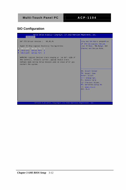
SIO Configuration
Chapter 3 AMI BIOS Setup 3-12
Mult i -Touch Panel PC A C P - 1 1 0 4
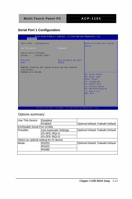
Serial Port 1 Configuration
Options summary:
Use This Device Disabled Enabled Optimal Default, Failsafe Default
En/Disable Serial Port (COM) Possible: Use Automatic Settings Optimal Default, Failsafe Default
IO=3F8; IRQ=4; IO=2F8; IRQ=3;
Select an optimal setting for IO device Mode: RS232 Optimal Default, Failsafe Default
RS422 RS485
Chapter 3 AMI BIOS Setup 3-13
Mult i -Touch Panel PC A C P - 1 1 0 4
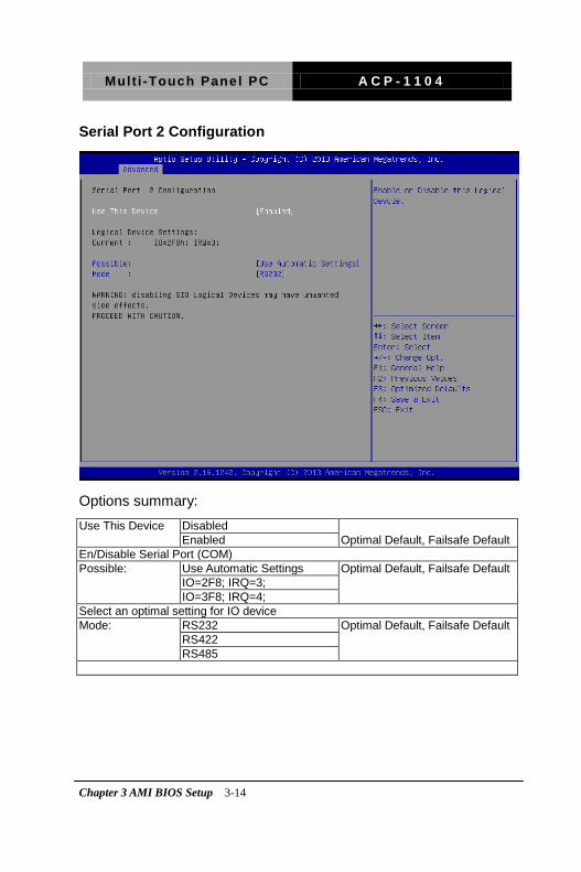
Serial Port 2 Configuration
Options summary: Use This Device Disabled
Enabled Optimal Default, Failsafe Default En/Disable Serial Port (COM) Possible: Use Automatic Settings Optimal Default, Failsafe Default
IO=2F8; IRQ=3; IO=3F8; IRQ=4;
Select an optimal setting for IO device Mode: RS232 Optimal Default, Failsafe Default
RS422 RS485
Chapter 3 AMI BIOS Setup 3-14
Mult i -Touch Panel PC A C P - 1 1 0 4
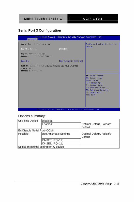
Serial Port 3 Configuration
Options summary: Use This Device Disabled
Enabled Optimal Default, Failsafe Default
En/Disable Serial Port (COM) Possible: Use Automatic Settings Optimal Default, Failsafe
Default IO=3E8; IRQ=11; IO=2E8; IRQ=11;
Select an optimal setting for IO device
Chapter 3 AMI BIOS Setup 3-15
Mult i -Touch Panel PC A C P - 1 1 0 4
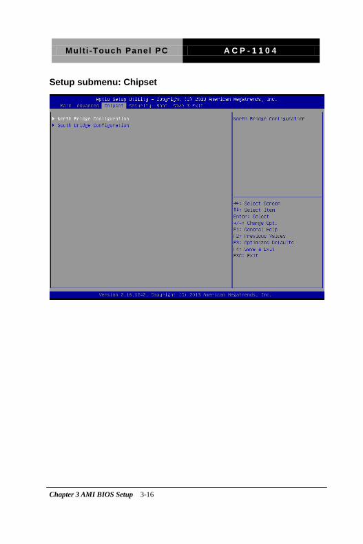
Setup submenu: Chipset
Chapter 3 AMI BIOS Setup 3-16
Mult i -Touch Panel PC A C P - 1 1 0 4
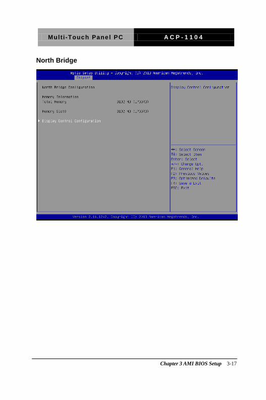
North Bridge
Chapter 3 AMI BIOS Setup 3-17
Mult i -Touch Panel PC A C P - 1 1 0 4
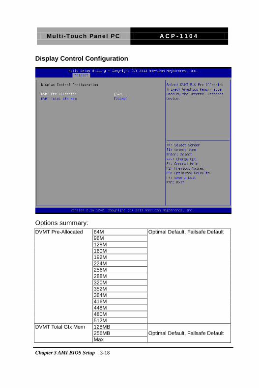
Display Control Configuration
Options summary: DVMT Pre-Allocated 64M Optimal Default, Failsafe Default
96M 128M 160M 192M 224M 256M 288M 320M 352M 384M 416M 448M 480M 512M
DVMT Total Gfx Mem 128MB 256MB Optimal Default, Failsafe Default Max
Chapter 3 AMI BIOS Setup 3-18
Mult i -Touch Panel PC A C P - 1 1 0 4
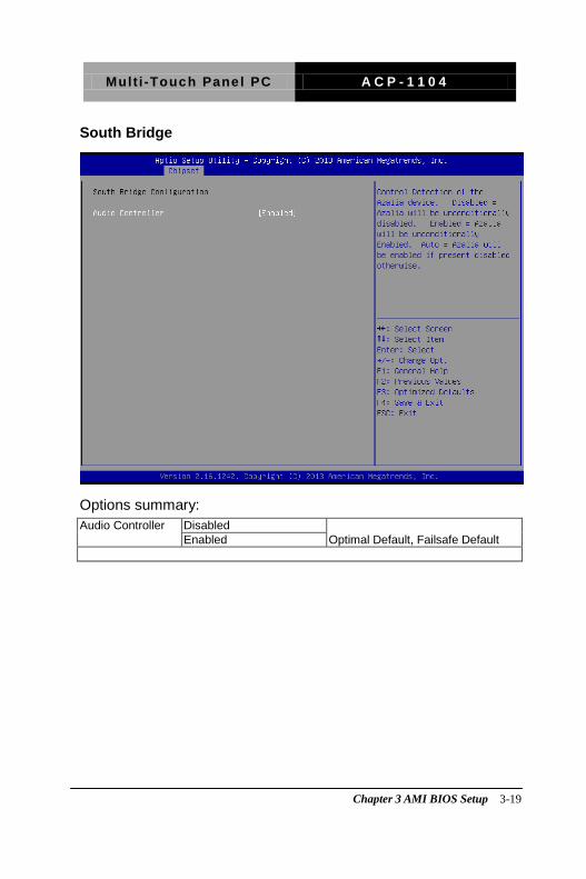
South Bridge
Options summary: Audio Controller Disabled
Enabled Optimal Default, Failsafe Default
Chapter 3 AMI BIOS Setup 3-19
Mult i -Touch Panel PC A C P - 1 1 0 4
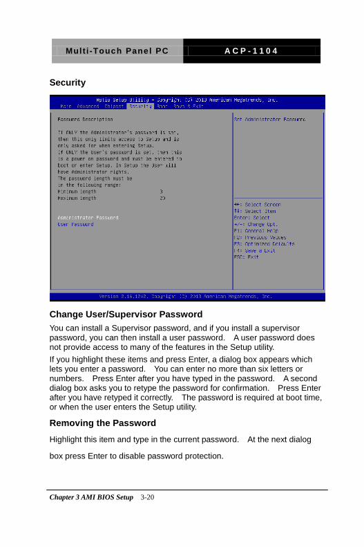
Security
Change User/Supervisor Password You can install a Supervisor password, and if you install a supervisor password, you can then install a user password. A user password does not provide access to many of the features in the Setup utility. If you highlight these items and press Enter, a dialog box appears which lets you enter a password. You can enter no more than six letters or numbers. Press Enter after you have typed in the password. A second dialog box asks you to retype the password for confirmation. Press Enter after you have retyped it correctly. The password is required at boot time, or when the user enters the Setup utility.
Removing the Password
Highlight this item and type in the current password. At the next dialog
box press Enter to disable password protection.
Chapter 3 AMI BIOS Setup 3-20
Mult i -Touch Panel PC A C P - 1 1 0 4
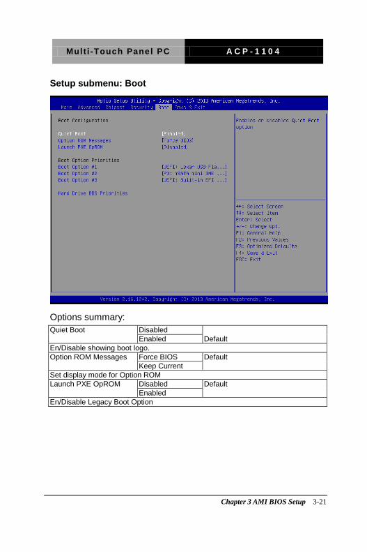
Setup submenu: Boot
Options summary: Quiet Boot Disabled
Enabled Default En/Disable showing boot logo. Option ROM Messages Force BIOS Default
Keep Current Set display mode for Option ROM Launch PXE OpROM Disabled Default
Enabled En/Disable Legacy Boot Option
Chapter 3 AMI BIOS Setup 3-21
Mult i -Touch Panel PC A C P - 1 1 0 4
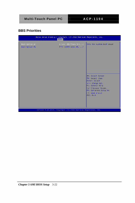
BBS Priorities
Chapter 3 AMI BIOS Setup 3-22
Mult i -Touch Panel PC A C P - 1 1 0 4
Setup submenu: Exit
Chapter 3 AMI BIOS Setup 3-23
Mult i -Touch Panel PC A C P - 1 1 0 4
Driver Installation
Chapter
4
Chapter 4 Driver Installation 4-1
Mult i -Touch Panel PC A C P - 1 1 0 4
The ACP-1104 comes with a driver disk that contains all drivers and
utilities that can help you setup your product.
Insert the disk and the installation guide will start automatically. If it
doesn’t, please follow the sequence below to install the drivers.
Follow the sequence below to install the drivers:
Step 1 – Install Chipset Driver
Step 2 – Install Graphics Driver
Step 3 – Install Network Driver
Step 4 – Install xHCI Driver (Windows® 7 only)
Step 5 – Install Intel Sideband Fabric Device Driver (Windows® 8.1
only)
Step 6 – Install Touch Driver
Please refer to the instructions below for further details.
Chapter 4 Driver Installation 4-2
Mult i -Touch Panel PC A C P - 1 1 0 4
4.1 Installation
Insert the ACP-1104 driver disk into the disk drive. And install the
drivers from Step 1 to Step 6 in order.
Step 1 – Install Chipset Driver
1. Open the Step 1 - Chipset folder followed by the
SetupChipset.exe file
2. Follow the instructions
3. Drivers will be installed automatically
Step 2 – Install Graphics Driver
1. Open the Step 2 - Graphics folder and select your OS
2. Open the Setup.exe file in the folder
3. Follow the instructions
4. Drivers will be installed automatically
Step 3 – Install Network Driver
1. Open the Step 3 - Network folder and select your OS
2. Open the.exe file in the folder
3. Follow the instructions
4. Drivers will be installed automatically
Step 4 – Install xHCI Driver (Windows® 7 only)
1. Open the Step 4 - xHCI folder and followed by the
Setup.exe file Chapter 4 Driver Installation 4-3
Mult i -Touch Panel PC A C P - 1 1 0 4
2. Follow the instructions
3. Drivers will be installed automatically
Step 5 – Install Intel Sideband Fabric Device Driver (Windows® 8.1
only)
1. Open the Step 5 - Intel Sideband Fabric Device
followed by the Setup.exe file
2. Follow the instructions
3. Drivers will be installed automatically
Step 6 – Install Touch Driver
1. Open the Step 6 - Touch folder followed by the
Setup.exe file
2. Follow the instructions
3. Drivers will be installed automatically
Chapter 4 Driver Installation 4-4

Mult i -Touch Panel PC A C P - 1 1 0 4
Programming the Watchdog Timer
Appendix
A
Appendix A Programming the Watchdog Timer A-1
Mult i -Touch Panel PC A C P - 1 1 0 4
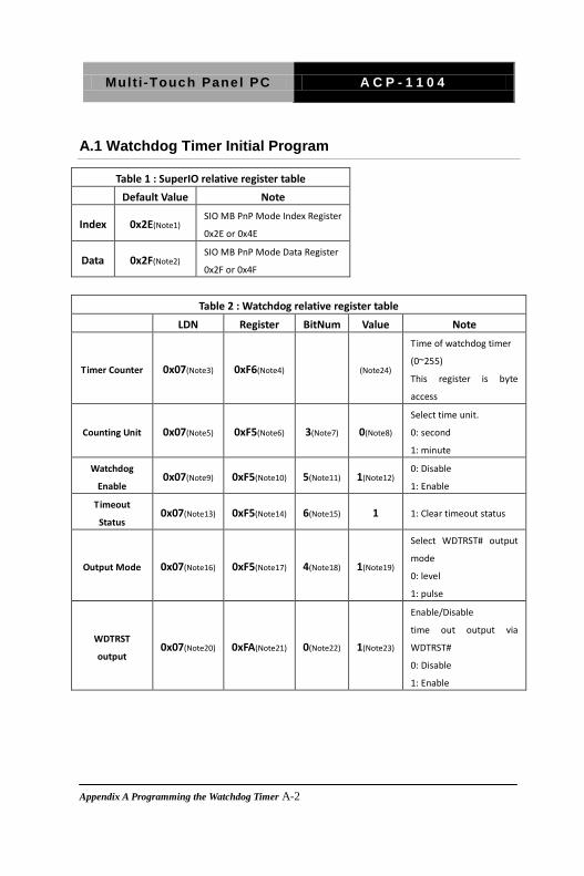
A.1 Watchdog Timer Initial Program
Table 1 : SuperIO relative register table Default Value Note
Index 0x2E(Note1) SIO MB PnP Mode Index Register
0x2E or 0x4E
Data 0x2F(Note2) SIO MB PnP Mode Data Register
0x2F or 0x4F
Table 2 : Watchdog relative register table
LDN Register BitNum Value Note
Timer Counter 0x07(Note3) 0xF6(Note4) (Note24)
Time of watchdog timer
(0~255)
This register is byte
access
Counting Unit 0x07(Note5) 0xF5(Note6) 3(Note7) 0(Note8) Select time unit.
0: second
1: minute
Watchdog
Enable 0x07(Note9) 0xF5(Note10) 5(Note11) 1(Note12)
0: Disable
1: Enable
Timeout
Status 0x07(Note13) 0xF5(Note14) 6(Note15) 1 1: Clear timeout status
Output Mode 0x07(Note16) 0xF5(Note17) 4(Note18) 1(Note19)
Select WDTRST# output
mode
0: level
1: pulse
WDTRST
output 0x07(Note20) 0xFA(Note21) 0(Note22) 1(Note23)
Enable/Disable
time out output via
WDTRST#
0: Disable
1: Enable
Appendix A Programming the Watchdog Timer A-2
Mult i -Touch Panel PC A C P - 1 1 0 4
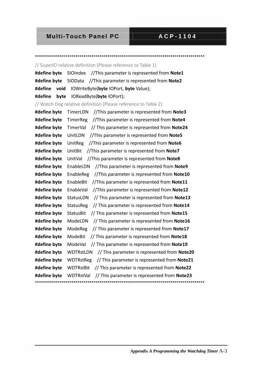
************************************************************************************ // SuperIO relative definition (Please reference to Table 1) #define byte SIOIndex //This parameter is represented from Note1 #define byte SIOData //This parameter is represented from Note2 #define void IOWriteByte(byte IOPort, byte Value); #define byte IOReadByte(byte IOPort); // Watch Dog relative definition (Please reference to Table 2) #define byte TimerLDN //This parameter is represented from Note3 #define byte TimerReg //This parameter is represented from Note4 #define byte TimerVal // This parameter is represented from Note24 #define byte UnitLDN //This parameter is represented from Note5 #define byte UnitReg //This parameter is represented from Note6 #define byte UnitBit //This parameter is represented from Note7 #define byte UnitVal //This parameter is represented from Note8 #define byte EnableLDN //This parameter is represented from Note9 #define byte EnableReg //This parameter is represented from Note10 #define byte EnableBit //This parameter is represented from Note11 #define byte EnableVal //This parameter is represented from Note12 #define byte StatusLDN // This parameter is represented from Note13 #define byte StatusReg // This parameter is represented from Note14 #define byte StatusBit // This parameter is represented from Note15 #define byte ModeLDN // This parameter is represented from Note16 #define byte ModeReg // This parameter is represented from Note17 #define byte ModeBit // This parameter is represented from Note18 #define byte ModeVal // This parameter is represented from Note19 #define byte WDTRstLDN // This parameter is represented from Note20 #define byte WDTRstReg // This parameter is represented from Note21 #define byte WDTRstBit // This parameter is represented from Note22 #define byte WDTRstVal // This parameter is represented from Note23 ************************************************************************************
Appendix A Programming the Watchdog Timer A-3
Mult i -Touch Panel PC A C P - 1 1 0 4
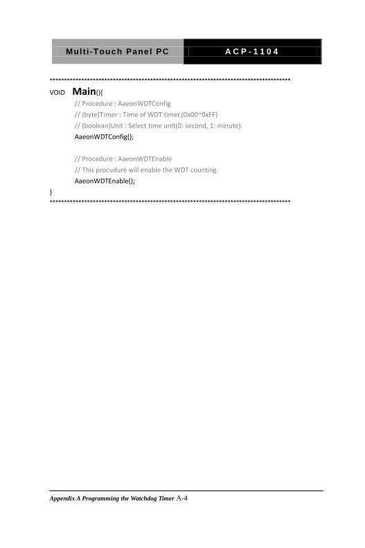
************************************************************************************ VOID Main(){ // Procedure : AaeonWDTConfig // (byte)Timer : Time of WDT timer.(0x00~0xFF) // (boolean)Unit : Select time unit(0: second, 1: minute). AaeonWDTConfig(); // Procedure : AaeonWDTEnable
// This procudure will enable the WDT counting. AaeonWDTEnable(); } ************************************************************************************
Appendix A Programming the Watchdog Timer A-4
Mult i -Touch Panel PC A C P - 1 1 0 4
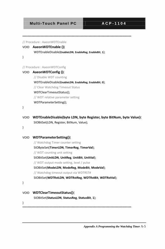
************************************************************************************ // Procedure : AaeonWDTEnable VOID AaeonWDTEnable (){
WDTEnableDisable(EnableLDN, EnableReg, EnableBit, 1); } // Procedure : AaeonWDTConfig VOID AaeonWDTConfig (){
// Disable WDT counting WDTEnableDisable(EnableLDN, EnableReg, EnableBit, 0); // Clear Watchdog Timeout Status WDTClearTimeoutStatus(); // WDT relative parameter setting WDTParameterSetting();
} VOID WDTEnableDisable(byte LDN, byte Register, byte BitNum, byte Value){ SIOBitSet(LDN, Register, BitNum, Value); } VOID WDTParameterSetting(){
// Watchdog Timer counter setting SIOByteSet(TimerLDN, TimerReg, TimerVal);
// WDT counting unit setting SIOBitSet(UnitLDN, UnitReg, UnitBit, UnitVal); // WDT output mode setting, level / pulse SIOBitSet(ModeLDN, ModeReg, ModeBit, ModeVal);
// Watchdog timeout output via WDTRST# SIOBitSet(WDTRstLDN, WDTRstReg, WDTRstBit, WDTRstVal);
} VOID WDTClearTimeoutStatus(){ SIOBitSet(StatusLDN, StatusReg, StatusBit, 1); } ************************************************************************************
Appendix A Programming the Watchdog Timer A-5
Mult i -Touch Panel PC A C P - 1 1 0 4
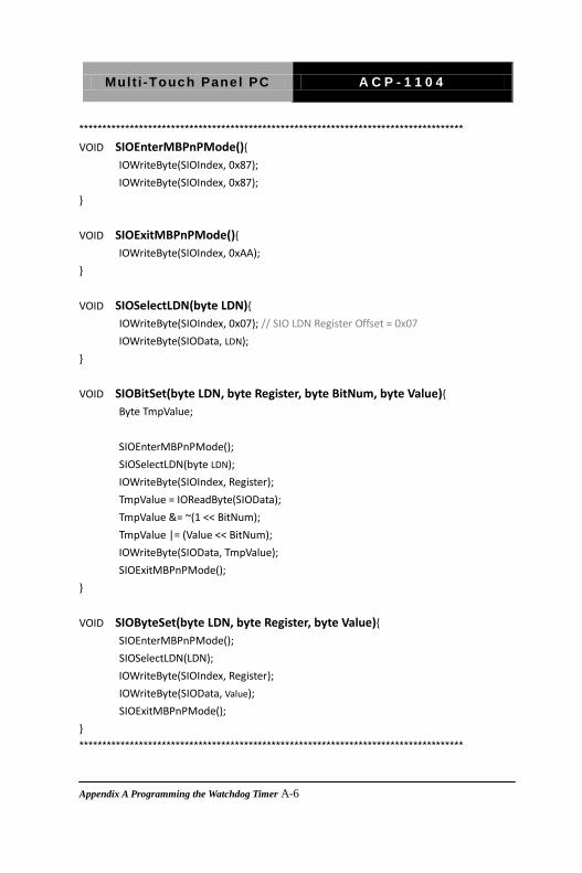
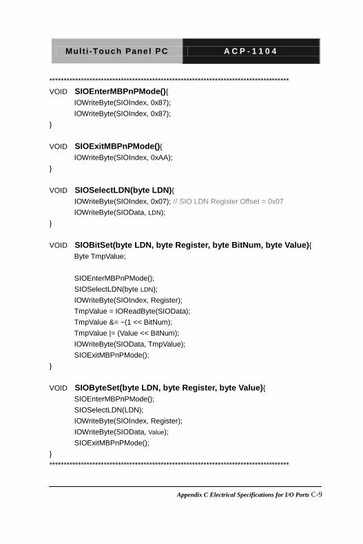
************************************************************************************ VOID SIOEnterMBPnPMode(){ IOWriteByte(SIOIndex, 0x87); IOWriteByte(SIOIndex, 0x87); } VOID SIOExitMBPnPMode(){ IOWriteByte(SIOIndex, 0xAA); } VOID SIOSelectLDN(byte LDN){
IOWriteByte(SIOIndex, 0x07); // SIO LDN Register Offset = 0x07 IOWriteByte(SIOData, LDN); } VOID SIOBitSet(byte LDN, byte Register, byte BitNum, byte Value){ Byte TmpValue; SIOEnterMBPnPMode();
SIOSelectLDN(byte LDN); IOWriteByte(SIOIndex, Register); TmpValue = IOReadByte(SIOData); TmpValue &= ~(1 << BitNum); TmpValue |= (Value << BitNum); IOWriteByte(SIOData, TmpValue); SIOExitMBPnPMode(); } VOID SIOByteSet(byte LDN, byte Register, byte Value){ SIOEnterMBPnPMode();
SIOSelectLDN(LDN); IOWriteByte(SIOIndex, Register);
IOWriteByte(SIOData, Value); SIOExitMBPnPMode();
} ************************************************************************************
Appendix A Programming the Watchdog Timer A-6
Mult i -Touch Panel PC A C P - 1 1 0 4
I/O Information
Appendix
B
Appendix B I/O Information B-1
Mult i -Touch Panel PC A C P - 1 1 0 4
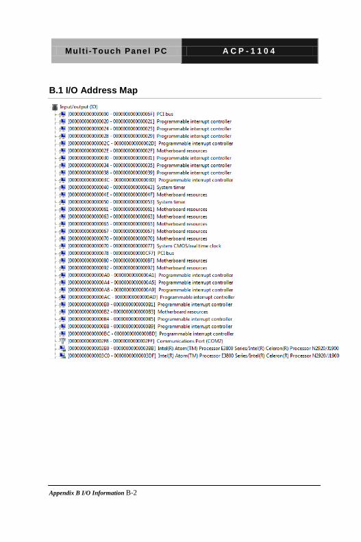
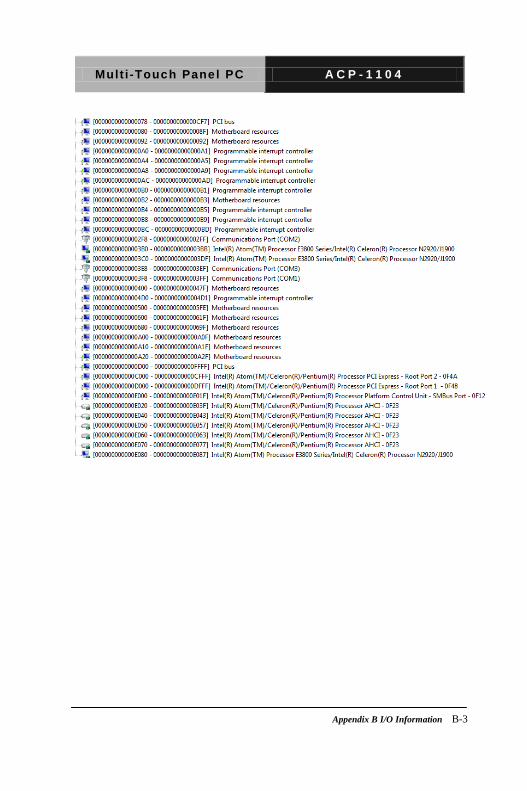
B.1 I/O Address Map
Appendix B I/O Information B-2
Mult i -Touch Panel PC A C P - 1 1 0 4
Appendix B I/O Information B-3
Mult i -Touch Panel PC A C P - 1 1 0 4
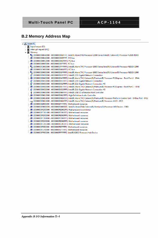
B.2 Memory Address Map
Appendix B I/O Information B-4
Mult i -Touch Panel PC A C P - 1 1 0 4
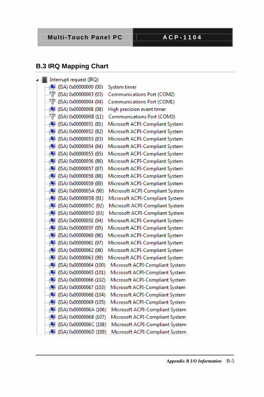
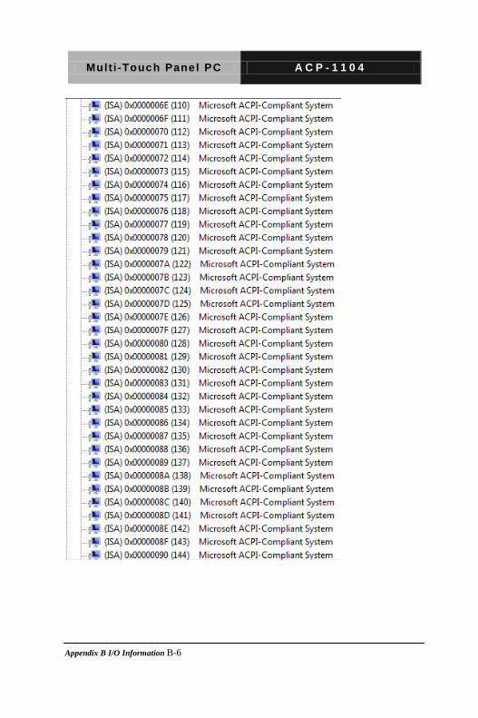
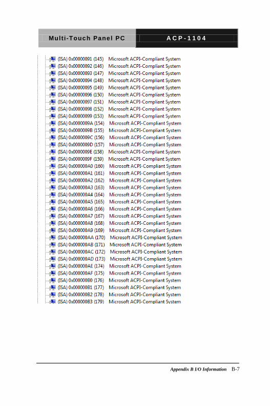
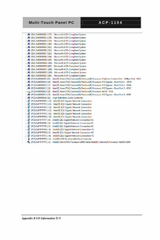
B.3 IRQ Mapping Chart
Appendix B I/O Information B-5
Mult i -Touch Panel PC A C P - 1 1 0 4
Appendix B I/O Information B-6
Mult i -Touch Panel PC A C P - 1 1 0 4
Appendix B I/O Information B-7
Mult i -Touch Panel PC A C P - 1 1 0 4
Appendix B I/O Information B-8
Mult i -Touch Panel PC A C P - 1 1 0 4
Electrical Specifications for I/O Ports
Appendix
C
Appendix C Electrical Specifications for I/O Ports C-1
Mult i -Touch Panel PC A C P - 1 1 0 4
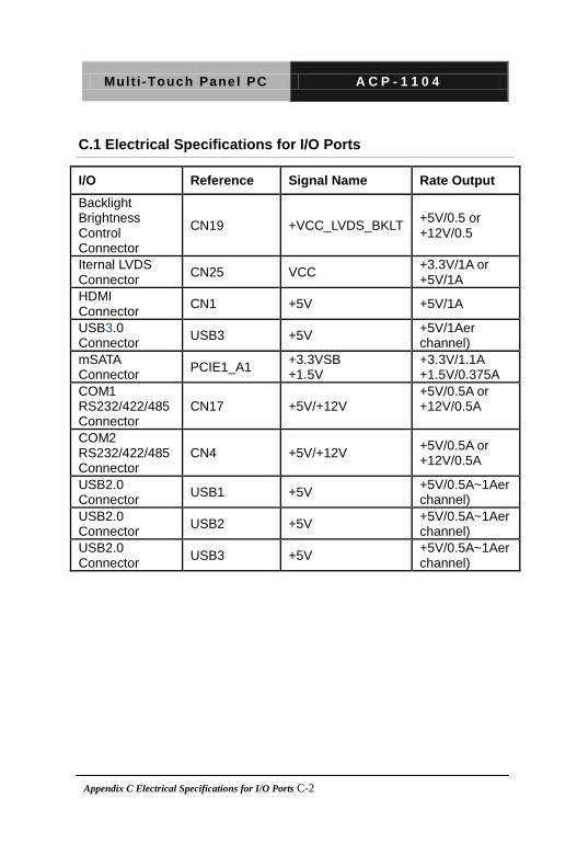
C.1 Electrical Specifications for I/O Ports
I/O Reference Signal Name Rate Output Backlight Brightness Control Connector
CN19 +VCC_LVDS_BKLT +5V/0.5 or +12V/0.5
Iternal LVDS Connector CN25 VCC +3.3V/1A or
+5V/1A HDMI Connector CN1 +5V +5V/1A
USB3.0 Connector USB3 +5V +5V/1Aer
channel) mSATA Connector PCIE1_A1 +3.3VSB
+1.5V +3.3V/1.1A +1.5V/0.375A
COM1 RS232/422/485 Connector
CN17 +5V/+12V +5V/0.5A or +12V/0.5A
COM2 RS232/422/485 Connector
CN4 +5V/+12V +5V/0.5A or +12V/0.5A
USB2.0 Connector USB1 +5V +5V/0.5A~1Aer
channel) USB2.0 Connector USB2 +5V +5V/0.5A~1Aer
channel) USB2.0 Connector USB3 +5V +5V/0.5A~1Aer
channel)
Appendix C Electrical Specifications for I/O Ports C-2
Mult i -Touch Panel PC A C P - 1 1 0 4
C.2 DIO Programming
ACP-1104 utilizes FINTEK 81866 chipset as its Digital I/O
controller.
Below are the procedures to complete its configuration and the
AAEON initial watchdog timer program is also attached based on
which you can develop customized program to fit your application.
There are three steps to complete the configuration setup: (1) Enter
the MB PnP Mode; (2) Modify the data of configuration registers; (3)
Exit the MB PnP Mode. Undesired result may occur if the MB PnP
Mode is not exited normally.(These three steps are the same as
programming WDT)
Appendix C Electrical Specifications for I/O Ports C-3
Mult i -Touch Panel PC A C P - 1 1 0 4
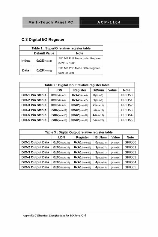
C.3 Digital I/O Register
Table 1 : SuperIO relative register table Default Value Note
Index 0x2E(Note1) SIO MB PnP Mode Index Register
0x2E or 0x4E
Data 0x2F(Note2) SIO MB PnP Mode Data Register
0x2F or 0x4F
Table 2 : Digital Input relative register table
LDN Register BitNum Value Note DIO-1 Pin Status 0x06(Note3) 0xA2(Note4) 0(Note5) GPIO50 DIO-2 Pin Status 0x06(Note6) 0xA2(Note7) 1(Note8) GPIO51 DIO-3 Pin Status 0x06(Note9) 0xA2(Note10) 2(Note11) GPIO52 DIO-4 Pin Status 0x06(Note12) 0xA2(Note13) 3(Note14) GPIO53 DIO-5 Pin Status 0x06(Note15) 0xA2(Note16) 4(Note17) GPIO54 DIO-5 Pin Status 0x06(Note18) 0xA2(Note19) 5(Note20) GPIO55
Table 3 : Digital Output relative register table
LDN Register BitNum Value Note DIO-1 Output Data 0x06(Note21) 0xA1(Note22) 0(Note23) (Note24) GPIO50 DIO-2 Output Data 0x06(Note25) 0xA1(Note26) 1(Note27) (Note28) GPIO51 DIO-3 Output Data 0x06(Note29) 0xA1(Note30) 2(Note31) (Note32) GPIO52 DIO-4 Output Data 0x06(Note33) 0xA1(Note34) 3(Note35) (Note36) GPIO53 DIO-5 Output Data 0x06(Note37) 0xA1(Note38) 4(Note39) (Note40) GPIO54 DIO-5 Output Data 0x06(Note41) 0xA1(Note42) 4(Note43) (Note44) GPIO55
Appendix C Electrical Specifications for I/O Ports C-4
Mult i -Touch Panel PC A C P - 1 1 0 4
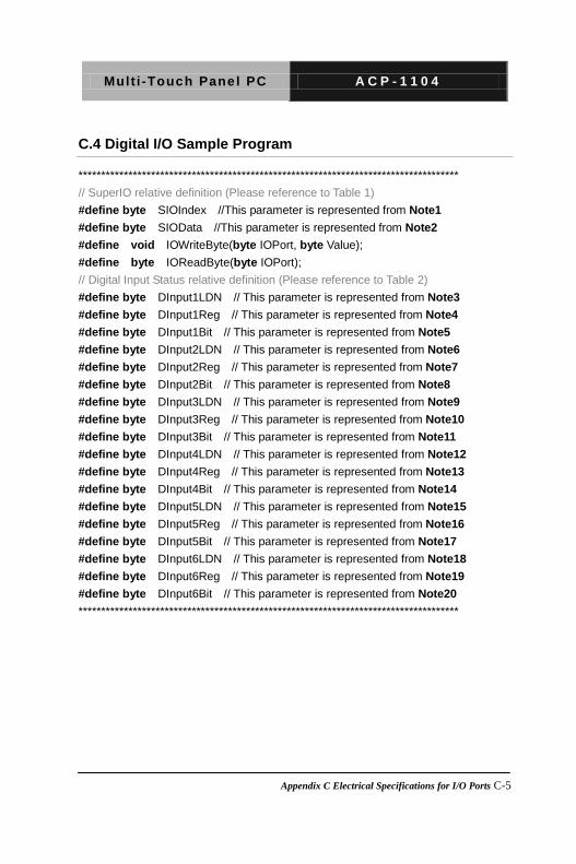
C.4 Digital I/O Sample Program
************************************************************************************ // SuperIO relative definition (Please reference to Table 1) #define byte SIOIndex //This parameter is represented from Note1 #define byte SIOData //This parameter is represented from Note2 #define void IOWriteByte(byte IOPort, byte Value); #define byte IOReadByte(byte IOPort); // Digital Input Status relative definition (Please reference to Table 2) #define byte DInput1LDN // This parameter is represented from Note3 #define byte DInput1Reg // This parameter is represented from Note4 #define byte DInput1Bit // This parameter is represented from Note5 #define byte DInput2LDN // This parameter is represented from Note6 #define byte DInput2Reg // This parameter is represented from Note7 #define byte DInput2Bit // This parameter is represented from Note8 #define byte DInput3LDN // This parameter is represented from Note9 #define byte DInput3Reg // This parameter is represented from Note10 #define byte DInput3Bit // This parameter is represented from Note11 #define byte DInput4LDN // This parameter is represented from Note12 #define byte DInput4Reg // This parameter is represented from Note13 #define byte DInput4Bit // This parameter is represented from Note14 #define byte DInput5LDN // This parameter is represented from Note15 #define byte DInput5Reg // This parameter is represented from Note16 #define byte DInput5Bit // This parameter is represented from Note17 #define byte DInput6LDN // This parameter is represented from Note18 #define byte DInput6Reg // This parameter is represented from Note19 #define byte DInput6Bit // This parameter is represented from Note20 ************************************************************************************
Appendix C Electrical Specifications for I/O Ports C-5
Mult i -Touch Panel PC A C P - 1 1 0 4
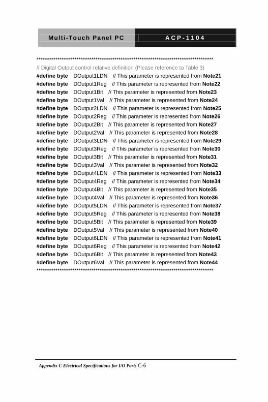
************************************************************************************ // Digital Output control relative definition (Please reference to Table 3) #define byte DOutput1LDN // This parameter is represented from Note21 #define byte DOutput1Reg // This parameter is represented from Note22 #define byte DOutput1Bit // This parameter is represented from Note23 #define byte DOutput1Val // This parameter is represented from Note24 #define byte DOutput2LDN // This parameter is represented from Note25 #define byte DOutput2Reg // This parameter is represented from Note26 #define byte DOutput2Bit // This parameter is represented from Note27 #define byte DOutput2Val // This parameter is represented from Note28 #define byte DOutput3LDN // This parameter is represented from Note29 #define byte DOutput3Reg // This parameter is represented from Note30 #define byte DOutput3Bit // This parameter is represented from Note31 #define byte DOutput3Val // This parameter is represented from Note32 #define byte DOutput4LDN // This parameter is represented from Note33 #define byte DOutput4Reg // This parameter is represented from Note34 #define byte DOutput4Bit // This parameter is represented from Note35 #define byte DOutput4Val // This parameter is represented from Note36 #define byte DOutput5LDN // This parameter is represented from Note37 #define byte DOutput5Reg // This parameter is represented from Note38 #define byte DOutput5Bit // This parameter is represented from Note39 #define byte DOutput5Val // This parameter is represented from Note40 #define byte DOutput6LDN // This parameter is represented from Note41 #define byte DOutput6Reg // This parameter is represented from Note42 #define byte DOutput6Bit // This parameter is represented from Note43 #define byte DOutput6Val // This parameter is represented from Note44 ************************************************************************************
Appendix C Electrical Specifications for I/O Ports C-6
Mult i -Touch Panel PC A C P - 1 1 0 4
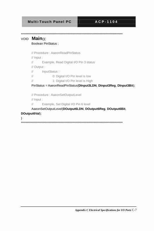
************************************************************************************ VOID Main(){ Boolean PinStatus ; // Procedure : AaeonReadPinStatus // Input : // Example, Read Digital I/O Pin 3 status
// Output : // InputStatus : // 0: Digital I/O Pin level is low // 1: Digital I/O Pin level is High
PinStatus = AaeonReadPinStatus(DInput3LDN, DInput3Reg, DInput3Bit); // Procedure : AaeonSetOutputLevel // Input : // Example, Set Digital I/O Pin 6 level AaeonSetOutputLevel(DOutput6LDN, DOutput6Reg, DOutput6Bit, DOutput6Val); } ************************************************************************************
Appendix C Electrical Specifications for I/O Ports C-7
Mult i -Touch Panel PC A C P - 1 1 0 4
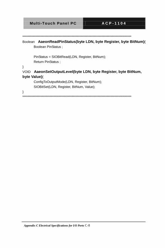
************************************************************************************ Boolean AaeonReadPinStatus(byte LDN, byte Register, byte BitNum){ Boolean PinStatus ; PinStatus = SIOBitRead(LDN, Register, BitNum); Return PinStatus ; } VOID AaeonSetOutputLevel(byte LDN, byte Register, byte BitNum, byte Value){ ConfigToOutputMode(LDN, Register, BitNum); SIOBitSet(LDN, Register, BitNum, Value); } ************************************************************************************
Appendix C Electrical Specifications for I/O Ports C-8
Mult i -Touch Panel PC A C P - 1 1 0 4
************************************************************************************ VOID SIOEnterMBPnPMode(){ IOWriteByte(SIOIndex, 0x87); IOWriteByte(SIOIndex, 0x87); } VOID SIOExitMBPnPMode(){ IOWriteByte(SIOIndex, 0xAA); } VOID SIOSelectLDN(byte LDN){
IOWriteByte(SIOIndex, 0x07); // SIO LDN Register Offset = 0x07 IOWriteByte(SIOData, LDN); } VOID SIOBitSet(byte LDN, byte Register, byte BitNum, byte Value){ Byte TmpValue; SIOEnterMBPnPMode();
SIOSelectLDN(byte LDN); IOWriteByte(SIOIndex, Register); TmpValue = IOReadByte(SIOData); TmpValue &= ~(1 << BitNum); TmpValue |= (Value << BitNum); IOWriteByte(SIOData, TmpValue); SIOExitMBPnPMode(); } VOID SIOByteSet(byte LDN, byte Register, byte Value){ SIOEnterMBPnPMode();
SIOSelectLDN(LDN); IOWriteByte(SIOIndex, Register);
IOWriteByte(SIOData, Value); SIOExitMBPnPMode();
} ************************************************************************************
Appendix C Electrical Specifications for I/O Ports C-9
Mult i -Touch Panel PC A C P - 1 1 0 4
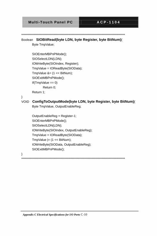
************************************************************************************ Boolean SIOBitRead(byte LDN, byte Register, byte BitNum){ Byte TmpValue; SIOEnterMBPnPMode();
SIOSelectLDN(LDN); IOWriteByte(SIOIndex, Register); TmpValue = IOReadByte(SIOData);
TmpValue &= (1 << BitNum); SIOExitMBPnPMode(); If(TmpValue == 0) Return 0; Return 1; } VOID ConfigToOutputMode(byte LDN, byte Register, byte BitNum){ Byte TmpValue, OutputEnableReg; OutputEnableReg = Register-1; SIOEnterMBPnPMode();
SIOSelectLDN(LDN); IOWriteByte(SIOIndex, OutputEnableReg); TmpValue = IOReadByte(SIOData); TmpValue |= (1 << BitNum); IOWriteByte(SIOData, OutputEnableReg); SIOExitMBPnPMode();
} ************************************************************************************
Appendix C Electrical Specifications for I/O Ports C-10