Embed Size (px)
Citation preview
ETRI Journal, Volume 38, Number 3, June 2016 © 2016 Chang-Soo Ahn et al. 417 http://dx.doi.org/10.4218/etrij.16.0115.0974
In this paper, an accurate characterization of a fabricated X-band transmit/receive module is described with the process of generating control data to correct amplitude and phase deviations in an active electronically scanned array antenna unit. In the characterization, quantization errors (from both a digitally controlled attenuator and a phase shifter) are considered using not theoretical values (due to discrete sets of amplitude and phase states) but measured values (of which implementation errors are a part). By using the presented procedure for the characterization, each initial control bit of both the attenuator and the phase shifter is closest to the required value for each array element position. In addition, each compensated control bit for the parasitic cross effect between amplitude and phase control is decided using the same procedure. Reduction of the peak sidelobe level of an array antenna is presented as an example to validate the proposed procedure.
Keywords: AESA antenna, T/R module, characterization, multi-function chip.
Manuscript received Nov. 12, 2015; revised Jan. 15, 2016; accepted Jan. 25, 2016. Chang-Soo Ahn ([email protected]) is with the Department of Computer and Radio
Communications Engineering, Korea University, Seoul, Rep. of Korea and the 3rd R&D Institute, ADD, Daejeon, Rep. of Korea.
Sang-Mi Chon ([email protected]) is with the ISR Center, LIGNEX1, Yongin, Rep. of Korea.
Seon-Joo Kim ([email protected]) is with the 3rd R&D Institute, ADD, Daejeon, Rep. of Korea. Young-Sik Kim ([email protected]) and Juseop Lee (corresponding author, juseoplee@
korea.ac.kr) are with the College of Informatics, Korea University, Seoul, Rep. of Korea.
I. Introduction
Active electronically scanned array (AESA) radars with transmit/receive (T/R) modules have been studied and developed for decades because they provide enhanced system functionality and performance compared to mechanically scanned array (MSA) radars [1]–[3].
An AESA radar implements rapid beam steering by independently setting the phase of each T/R module’s phase shifter (each T/R module is connected to an array element), whereas an MSA radar is limited to beam steering by using hydraulically or electrically controlled gimbal to physically move the array for search.
In addition, an AESA radar can control the shape of an antenna beam by adjusting the amplitude of attenuators in T/R modules connected to each array element [4]. Thus, an AESA radar has improved search and track performance because of beam agility [5].
Figure 1 shows the configuration of an AESA antenna unit in a radar system [6]–[8]. Radar systems usually have a separate receive beamformer for each monopulse beam for angle tracking of targets, such as sum (Ʃ), azimuth difference (ΔAz), and elevation difference (ΔEl). In addition, a guard channel is applied to blank sidelobe detection. The AESA antenna unit consists of radiating elements and an antenna structure; T/R modules and associated control circuitry; RF beamformers; DC power distribution; and a beam steering controller.
Because there are usually hundreds or thousands of radiators
Accurate Characterization of T/R Modules with Consideration of Amplitude/Phase Cross Effect in
AESA Antenna Unit
Chang-Soo Ahn, Sang-Mi Chon, Seon-Joo Kim, Young-Sik Kim, and Juseop Lee
418 Chang-Soo Ahn et al. ETRI Journal, Volume 38, Number 3, June 2016 http://dx.doi.org/10.4218/etrij.16.0115.0974
Fig. 1. Configuration of AESA antenna unit in radar system.
Part of radar system
AESA antenna unit
Radarcomputer
and display
Signal processor
receiver
△Azreceiver
△Elreceiver
Guardreceiver
Beamformers
DC/DCdistribution
Logicdistribution
T/Rmodules
Controlelectronics
DC/DC
Exciter
Beamsteeringcontroller
AC-to-DC convertersand transformers
System power
Tx
Antennastructure
Radiating elements
△Az
△El
Guard
and T/R modules, and a lot of networks connecting them, in an AESA antenna unit, considerable amplitude and phase differences among the paths from each array element to each receive beamformer output are produced; these differences can cause degradation of radiation performance.
In general, degradation of radiation performance of an AESA antenna unit occurs due to the quantization of both amplitude taper and phase shift at each array element [9].
Several methods have been proposed to enhance antenna gain and achieve more precise beam pointing and broader null forming [10]–[12].
In this paper, an accurate characterization of a fabricated X-band T/R module with a multi-function chip is presented to improve the radiation performance of an AESA antenna unit.
The process through which to generate control data that is to be read by the multi-function chip is described through several steps. In particular, we describe the procedure to derive each initial control bit of both the attenuator and the phase shifter, taking into consideration the implementation errors of the T/R module. It is also shown that each control bit for the compensation of the parasitic cross effect between amplitude and phase control of the T/R module can be derived using the same procedure.
A 16 by 16 planar array antenna unit with T/R modules is considered to verify the proposed procedure. It is shown that the proposed procedure can reduce the peak sidelobe level of the array antenna unit.
II. Generation of Control Data in AESA Antenna Unit
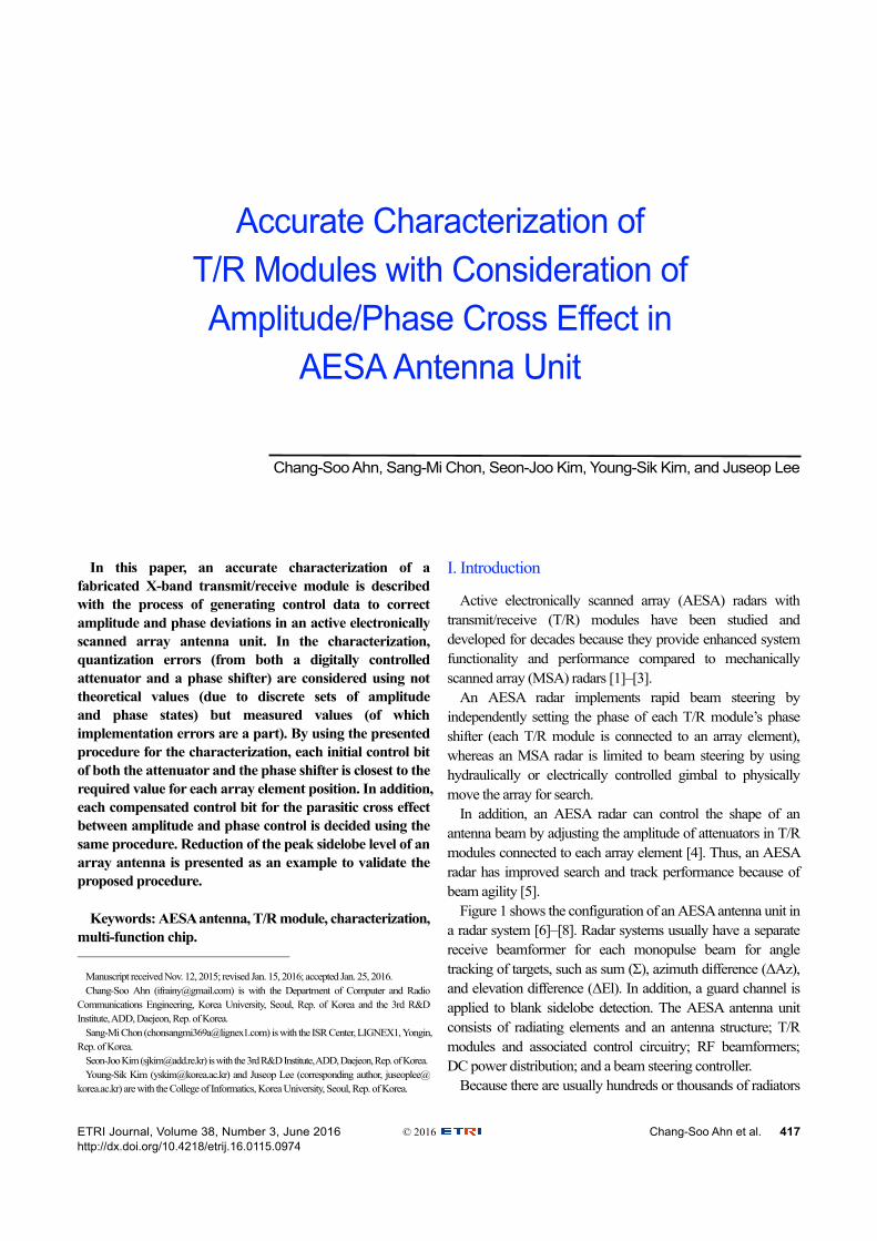
An AESA antenna unit should generate and calculate control data in T/R modules responding to beam-control parameters for specified beam shapes and directions [13]. The generation of control data in an AESA antenna unit can be described as shown in Fig. 2.
In the first step, a set of desired settings (without any imperfections) for the array elements is generated from an “Antenna generator” function. The set of desired settings depends on several factors, such as main beam direction (u, v), center frequency, taper information for beam shape, antenna map, and active element pattern, as indicated in Fig. 2.
An antenna map features a set of vectors — one for each array element that commences in the array antenna phase center and ends in the element phase center. The “active element pattern” function describes the radiation pattern for each array element, when placed in the array surrounded by all neighboring elements [14].
The parameters u and v indicate the direction of a beam within a sine-space coordinate system. Sine space is a hemispherical projection of three-dimensional space onto a plane of an array [9].
In the second step, a calibration value stored in the “Antenna Correction” function is subtracted from the set of desired settings. This subtraction results in a new set of desired settings, which we call “corrected desired settings.”
ETRI Journal, Volume 38, Number 3, June 2016 Chang-Soo Ahn et al. 419 http://dx.doi.org/10.4218/etrij.16.0115.0974
Fig. 2. Generation of control data and usage of calibration data inAESA antenna unit.
+Antenna generator
Stateselector
T/R modulecharacterization
dataAntenna
correction
Beam data
Calibration
Frequency
Taper
Antennamap
Direction u, vActive element pattern
Desired settings
Correcteddesired settings-
Control data
Serial no. map
Table 1. Error sources of amplitude and phase deviation in AESA array unit.
Error source Error type
T/R modules Non-linear
Difference between T/R modules and networks for dividing and combining
Linear
Difference for beamformers Linear
Manufacturing tolerance of radiating elements spacing Linear
Difference by connection between T/R modules and radiating elements
Linear
An antenna correction table containing phase and amplitude
correction values for each frequency is constructed. The correction values are amassed on a near-field antenna test range using a method known as single element adjustment [15], [16].
Table 1 shows the error sources of the amplitude and phase differences among the paths from each array element to each receive beamformer output. All error sources except for “T/R modules” are linear and can finally be corrected through a near-field antenna test. The error by “T/R modules” is nonlinear; thus, the characterization described in Section III is necessary.
Prior to the commencement of data collection for the antenna correction table, it is required that the T/R module characterization data is updated with the latest available data for all currently installed T/R modules. In the last step, the corrected desired settings are converted to control data. This conversion is preferably executed in each T/R module as it is dependent normally on both the temperatures and the serial numbers of the T/R modules. The temperature of each T/R module can be measured internally, and a T/R module’s serial number should preferably be stored within its own non-volatile memories to facilitate the replacement of T/R modules without the need, for example, to update an externally stored database. Figure 3 shows how data and calculations can be placed in the different components.
T/R modulecharacterization
data
Flash PROM
FPGA
Beam computations, control functions
Taper,antenna calibration data
Block RAM
Working memory
SDRAM
Fig. 3. Hardware components, and placement of data and calculations.
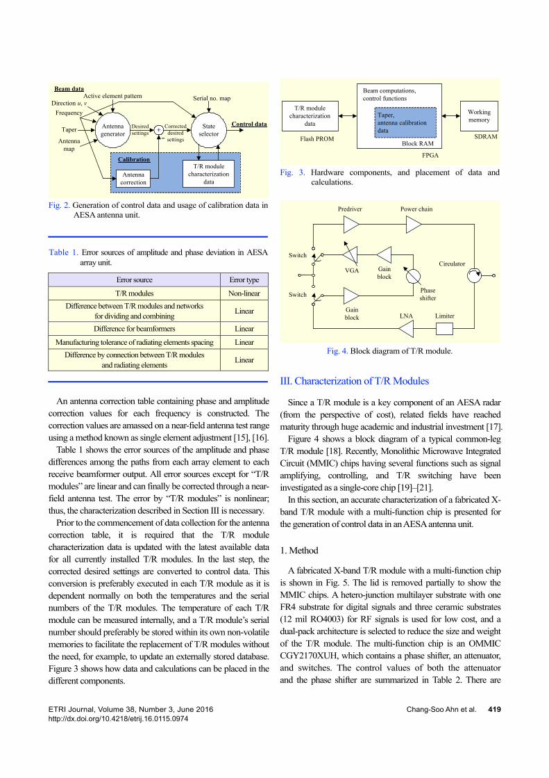
Fig. 4. Block diagram of T/R module.
Phaseshifter
Gainblock
Gainblock
VGA
LNA Limiter
Circulator
Power chainPredriver
Switch
Switch
III. Characterization of T/R Modules
Since a T/R module is a key component of an AESA radar (from the perspective of cost), related fields have reached maturity through huge academic and industrial investment [17].
Figure 4 shows a block diagram of a typical common-leg T/R module [18]. Recently, Monolithic Microwave Integrated Circuit (MMIC) chips having several functions such as signal amplifying, controlling, and T/R switching have been investigated as a single-core chip [19]–[21].
In this section, an accurate characterization of a fabricated X-band T/R module with a multi-function chip is presented for the generation of control data in an AESA antenna unit.
1. Method
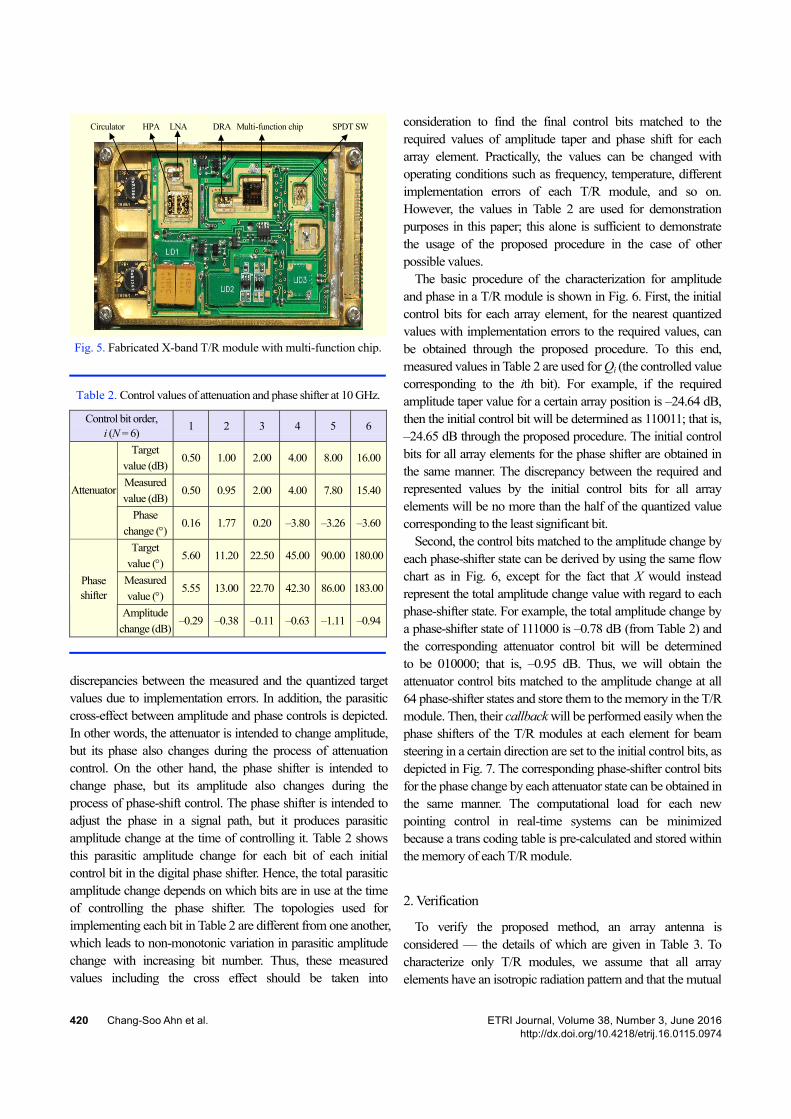
A fabricated X-band T/R module with a multi-function chip is shown in Fig. 5. The lid is removed partially to show the MMIC chips. A hetero-junction multilayer substrate with one FR4 substrate for digital signals and three ceramic substrates (12 mil RO4003) for RF signals is used for low cost, and a dual-pack architecture is selected to reduce the size and weight of the T/R module. The multi-function chip is an OMMIC CGY2170XUH, which contains a phase shifter, an attenuator, and switches. The control values of both the attenuator and the phase shifter are summarized in Table 2. There are
420 Chang-Soo Ahn et al. ETRI Journal, Volume 38, Number 3, June 2016 http://dx.doi.org/10.4218/etrij.16.0115.0974
Fig. 5. Fabricated X-band T/R module with multi-function chip.
Circulator HPA LNA Multi-function chip SPDT SWDRA
Table 2. Control values of attenuation and phase shifter at 10 GHz.
Control bit order, i (N = 6)
1 2 3 4 5 6
Target
value (dB) 0.50 1.00 2.00 4.00 8.00 16.00
Measured
value (dB) 0.50 0.95 2.00 4.00 7.80 15.40Attenuator
Phase
change () 0.16 1.77 0.20 –3.80 –3.26 –3.60
Target
value () 5.60 11.20 22.50 45.00 90.00 180.00
Measured
value () 5.55 13.00 22.70 42.30 86.00 183.00
Phase shifter
Amplitude
change (dB) –0.29 –0.38 –0.11 –0.63 –1.11 –0.94
discrepancies between the measured and the quantized target values due to implementation errors. In addition, the parasitic cross-effect between amplitude and phase controls is depicted. In other words, the attenuator is intended to change amplitude, but its phase also changes during the process of attenuation control. On the other hand, the phase shifter is intended to change phase, but its amplitude also changes during the process of phase-shift control. The phase shifter is intended to adjust the phase in a signal path, but it produces parasitic amplitude change at the time of controlling it. Table 2 shows this parasitic amplitude change for each bit of each initial control bit in the digital phase shifter. Hence, the total parasitic amplitude change depends on which bits are in use at the time of controlling the phase shifter. The topologies used for implementing each bit in Table 2 are different from one another, which leads to non-monotonic variation in parasitic amplitude change with increasing bit number. Thus, these measured values including the cross effect should be taken into
consideration to find the final control bits matched to the required values of amplitude taper and phase shift for each array element. Practically, the values can be changed with operating conditions such as frequency, temperature, different implementation errors of each T/R module, and so on. However, the values in Table 2 are used for demonstration purposes in this paper; this alone is sufficient to demonstrate the usage of the proposed procedure in the case of other possible values.
The basic procedure of the characterization for amplitude and phase in a T/R module is shown in Fig. 6. First, the initial control bits for each array element, for the nearest quantized values with implementation errors to the required values, can be obtained through the proposed procedure. To this end, measured values in Table 2 are used for Qi (the controlled value corresponding to the ith bit). For example, if the required amplitude taper value for a certain array position is –24.64 dB, then the initial control bit will be determined as 110011; that is, –24.65 dB through the proposed procedure. The initial control bits for all array elements for the phase shifter are obtained in the same manner. The discrepancy between the required and represented values by the initial control bits for all array elements will be no more than the half of the quantized value corresponding to the least significant bit.
Second, the control bits matched to the amplitude change by each phase-shifter state can be derived by using the same flow chart as in Fig. 6, except for the fact that X would instead represent the total amplitude change value with regard to each phase-shifter state. For example, the total amplitude change by a phase-shifter state of 111000 is –0.78 dB (from Table 2) and the corresponding attenuator control bit will be determined to be 010000; that is, –0.95 dB. Thus, we will obtain the attenuator control bits matched to the amplitude change at all 64 phase-shifter states and store them to the memory in the T/R module. Then, their callback will be performed easily when the phase shifters of the T/R modules at each element for beam steering in a certain direction are set to the initial control bits, as depicted in Fig. 7. The corresponding phase-shifter control bits for the phase change by each attenuator state can be obtained in the same manner. The computational load for each new pointing control in real-time systems can be minimized because a trans coding table is pre-calculated and stored within the memory of each T/R module.
2. Verification
To verify the proposed method, an array antenna is considered — the details of which are given in Table 3. To characterize only T/R modules, we assume that all array elements have an isotropic radiation pattern and that the mutual
ETRI Journal, Volume 38, Number 3, June 2016 Chang-Soo Ahn et al. 421 http://dx.doi.org/10.4218/etrij.16.0115.0974
Fig. 6. Basic procedure for characterization of T/R module.
Start
Calculate the required value at the array element position and store it X
Set all control bits to 0
i = N
Compare the stored value withthe controlled value corresponding to ith bit
|X| = Qi
Change the stored value to |X|–Qi
X = |X|–Qi
Set ith bit to 1
i = i–1
i = 0
Compare the stored value with Q1/2X > Q1/2
j = 1, k = 0
Check if jth bit is 0
Set jth bit to 0Set jth bit to 1
k = k+1
k = 1
End
j = j+1
No
Yes
No
Yes
No
Yes
No
Yes
Yes No
Fig. 7. Compensation of amplitude change by phase shifter.
Phase-shiftercontrol settings P1 P2 P3 P4 P5 P6
Phase control
Stored amplitudechange by eachphase-shift bit
ROM
Attenuation distortion
compensationC1 C2 C3 C4 C5 C6
Attenuatorcontrol settings A1 A2 A3 A4 A5 A6
+
–Amplitude
control
Table 3. Parameters of AESA antenna unit in analysis.
Parameter Value
Type Planar array
Number of elements 16 × 16
Element grid Triangular grid
Element spacing dx = 19.5 mm, dy = 14.7 mm
Amplitude weighting –30 dB Taylor distribution, 5n
Fig. 8. Peak sidelobe levels of array antenna for number of beam steering cases under assumption that T/R modules are operated using initial control bits without cross effect, with phase cross effect, and with amplitude/phase cross effect, respectively.
1 11 21 31 41 51 61 71 81 91 101 111 121 131 141 151 161 169–32
–31
–30
–29
–28
–27
–26
–25
–24
–23
–22
–21
Beam steering case number
Pea
k si
delo
be le
vel (
dB)
Using initial control bit w/o cross effect Using initial control bit w phase cross effect Using initial control bit w amplitude/phase cross effect
coupling between them is neglected.
Peak sidelobe levels of the array antenna for a number of beam steering cases are shown in Fig. 8, where T/R modules are operated using initial control bits. The beam steering cases in Fig. 8 represent that the array antenna steers a beam in an orderly manner in 5 increments from −30 to +30 in both azimuth and elevation angles. In other words, the beam steering case numbers #1 and #2 represent that the array antenna is directed to (−30, −30) and (−25, −30) in azimuth and elevation angles, respectively. Thus, the beam steering case numbers #85 and #169 represent that the array antenna steers the beam at (0, 0) and (+30, +30) in azimuth and elevation angles, respectively.
The thin solid line in Fig. 8 shows the peak sidelobe level when initial control bits for a −30 dB peak sidelobe level are used under the assumption that there is no cross effect. The peak sidelobe level is higher than the desired value due to both the quantization and implementation errors. The maximum peak sidelobe level in this case is −26.15 dB at beam steering case #81; that is, (−20, 0) direction.

422 Chang-Soo Ahn et al. ETRI Journal, Volume 38, Number 3, June 2016 http://dx.doi.org/10.4218/etrij.16.0115.0974
Table 4. Values obtained from procedure for compensated control bit of attenuator at first array element.
Parameter Value
Required attenuation 26.74 dB
Initial control bits for the attenuator (A) 111011
Measured attenuation with A 26.65 dB
Required phase shift 243.00
Initial control bits for the phase shifter (B) 110101
Measured phase shift with B 243.85
Amplitude change with B (C) –2.24 dB
Control bit matched to C 001000
Compensated control bits for the attenuator (D) 110011
Measured attenuation with D 24.65 dB
Resultant attenuation (C + D) 26.89 dB
Fig. 9. Peak sidelobe levels of array antenna for number of beamsteering cases, under assumption that T/R modules are operated using initial control bits without cross effect andcompensated control bits with amplitude/phase crosseffect, respectively.
1 11 21 31 41 51 61 71 81 91 101 111 121 131 141 151 161 169–32
–31
–30
–29
–28
–27
–26
–25
–24
–23
–22
–21
Beam steering case number
Pea
k si
delo
be le
vel (
dB)
Using initial control bit w/o cross effect Using compensated control bit w amplitude/phase cross efect
The dotted line in Fig. 8 shows the peak sidelobe level when the cross effect of the attenuator comes into play. The additional phase change by the initial control bits of the attenuators for each array element are added to the phase by the initial control bits of the phase shifters. It shows there is little difference from the first case.
The thick solid line in Fig. 8 shows the peak sidelobe level when both the cross effect of the attenuator and the cross effect of the phase shifter accur. The peak sidelobe level in this case is largely degraded, and the array antenna has a maximum peak sidelobe level of −21.6 dB in the case of beam steering case #79; that is, (−30, 0) direction. The peak sidelobe level with
cross effect of the phase shifter is not shown for the sake of clarity within the figure; it is similar to the third case.
Thus, compensation of amplitude change through control of the phase shifter is only required for improvement of the peak sidelobe level. The compensated control bits can be obtained by subtracting the control bits matched to the amplitude change by each phase-shifter state (as described in Section III) from the initial control bits for the attenuators. Table 4 shows the values obtained from the procedure for the compensated control bit of the attenuator at the first array element when the beam of the antenna unit in Table 3 is directed to (−30, −30), for example. It is verified that the resultant attenuation of the T/R module at the array element is close to the required value from the theoretical calculation through the procedure.
The dotted line in Fig. 9 shows the peak sidelobe level when compensated control bits (to reduce the cross effect of the phase shifter) are used, under the assumption that both types of cross effect are in existence. The peak sidelobe level in this case is similar to the first case in Fig. 8. The maximum peak sidelobe level is −25.71 dB in the case of beam steering case #87; that is, (+10, 0) direction.
Obviously, the compensated control bits of the attenuators cause the additional phase changes. However, the related beam pointing error is negligible when a 6-bit phase shifter is utilized in the antenna unit (comprising 256 elements) [8], [22]–[24].
IV. Conclusion
The generation process of control data for corrected settings of the amplitude and phase in an AESA antenna unit is described for desired and accurate beam shaping and steering. In particular, an accurate, practical characterization using data from a fabricated X-band T/R module with a multi-function chip is presented — the likes of which is invaluable to engineers who are working on calibrations of AESA antennas. Each initial control bit of both the attenuator and the phase shifter is derived through the proposed procedure. It represents the realizable and closest value to the desired amplitude and phase for each array element. In addition, each compensated control bit for the parasitic cross-effect between amplitude and phase control is decided in the same manner. Reduction of the peak sidelobe level of an array antenna using the compensated control bit is verified.
References
[1] A. Farina et al., “AESA Radar-Pan-Domain Multi-function
Capabilities for Future Systems,” IEEE Int. Symp. Phased Array
Syst. Technol., Waltham, MA, USA, Oct. 15–18, 2013, pp. 411.
ETRI Journal, Volume 38, Number 3, June 2016 Chang-Soo Ahn et al. 423 http://dx.doi.org/10.4218/etrij.16.0115.0974
[2] P. Sgambato et al., “System Manager for AESA Radar Systems,”
IEEE Radar Conf., Arlington, VA, USA, May 10–15, 2015, pp.
1734–1738.
[3] R. Bil and W. Holpp, “Naval Radar Trends: a Look Back-a Look
Forward,” Int. Radar Symp., Dresden, Germany, June 24–26,
2015, pp. 13–19.
[4] E.R. Billam, “MESAR-the Application of Modern Technology to
Phased Array Radar,” presented at the IEE Tutorial Meeting
Phased Array Radar, London, UK, Sept. 18, 1989, pp. 5/1–5/16.
[5] R. Hendrix, “Aerospace System Improvements Enabled by
Modern Phased Array Radar-2008,” IEEE Int. Radar Conf.,
Rome, Italy, May 26–30, 2008, pp. 1–6.
[6] A.K. Agrawal et al., “Active Phased Array Antenna Development
for Modern Shipboard Radar System,” Johns Hopkins APL Tech.
Dig., vol. 22, no. 4, 2001, pp. 600–613.
[7] A.K. Agrawal and E.L. Holzman, “Beamformer Architectures for
Active Phased-Array Radar Antennas,” IEEE Trans. Antennas
Propag., vol. 47, no. 3, Mar. 1999, pp. 432–442.
[8] M. Skolnik, “Introduction to Radar Systems,” 3rd ed., New York,
NY, USA: McGraw-Hill, 2001.
[9] A.D. Brown, “Electroncially Scanned Arrays MATLAB Modeling
and Simulation,” Boca Raton, FL, USA: CRC Press, 2012.
[10] S.H. Son, W. Hwang, and S.I. Jeon, “Gain Enhancement of Large
Phased Array Antennas by Phase Error Correction,” IEEE
Antennas Propag. Soc. Int. Symp., Honolulu, HI, USA, June 9–15,
2007, pp. 137–140.
[11] W. Jiang et al., “Comparison of Random Phasing Methods for
Reducing Beam Pointing Errors in Phased Array,” IEEE Trans.
Antennas Propag., vol. 51, no. 4, Apr. 2003, pp. 782–787.
[12] N. Nakamoto et al., “Phase Optimization for Accurate Beam
Forming of Phased Array with Element Field Errors at Every
Phase Shift,” IEEE Int. Symp. Phased Array Syst. Technol.,
Waltham, MA, USA, Oct. 15–18, 2013, pp. 693–697.
[13] P.N. Drackner and B. Engstrom, “An Active Antenna
Demonstrator for Future AESA-Systems,” IEEE Int. Radar Conf.,
Arlington, VA, USA, May 9–12, 2005, pp. 226–231.
[14] D.M. Pozar, “The Active Element Pattern,” IEEE Trans.
Antennas Propag., vol. 42, no. 8, Aug. 1994, pp. 1176–1178.
[15] S. Moore et al., “AMSAR Active Phased Array Antenna,” IET Int.
Conf. Radar Syst., Edinburgh, UK, Oct. 15–18, 2007, pp. 1–4.
[16] I. Seker, “Calibration Methods for Phased Array Radars,” Proc.
SPIE, vol. 8714, May 2013, pp. 1–15.
[17] M. Pirkl and W. Holpp, “From Research to Application: How
Phased Array Radars Conquered the Real World,” Int. Radar
Symp., Dresden, Germany, June 19–21, 2013, pp. 17–21.
[18] A. Agrawal, R. Clark, and J. Komiak, “T/R Module Architecture
Tradeoffs for Phased Array Antennas,” IEEE MTT-S Int.
Microw. Symp. Dig., San Francisco, CA, USA, June 17–21, 1996,
pp. 995–998.
[19] W. Ciccognani et al., “A Compact High Performance X-Band
Core-Chip with on Board Serial-to-Parallel Conversion,”
European Mircrowave Conf., Paris, France, Sept. 28–30, 2010, pp.
902–905.
[20] J.-C. Jeong et al., “An S-Band Multifunction Chip with a Simple
Interface for Active Phased Array Base Station Antennas,” ETRI
J., vol. 35, no. 3, June 2013, pp. 378–385.
[21] T. Dinc et al., “X-Band SiGe Bi-Complementary Metal-Oxide
Semiconductor Transmit/Receive Module Core Chip for Phased
Array Radar Applications,” IET Microw., Antennas Propag., vol.
9, no. 9, June 2015, pp. 948–956.
[22] C.J. Miller, “Minimizing the Effects of Phase Quantization in an
Electronically Scanned Array,” Proc. Symp. Electronically
Scanned Array Techn. Appl., Rome, NY, USA, July 1964, pp.
1738.
[23] R.J. Mailloux, “Phased Array Antenna Handbook,” 2nd ed.,
Norwood, MA, USA: Artech House, 2005.
[24] K.R. Carver, W. Cooper, and W. Stutzman, “Beam Pointing
Errors of Planar Phased Arrays,” IEEE Trans. Antennas Propag.,
vol. 21, no.2, Mar. 1973, pp. 199–202.

424 Chang-Soo Ahn et al. ETRI Journal, Volume 38, Number 3, June 2016 http://dx.doi.org/10.4218/etrij.16.0115.0974
Chang-Soo Ahn received his BS and MS
degrees in electrical engineering from Korea
University, Seoul, Rep. of Korea, in 2002 and
2005, respectively, and is currently working
toward his PhD degree at Korea University. In
2005, he joined the Agency for Defense
Development, Daejeon, Rep. of Korea, where
he is currently a senior researcher. His research interests include
airborne AESA radar system design and analysis, operational modes
design, and radar resource management.
Sang-Mi Chon received her PhD degree in
electrical engineering from Pohang University
of Science and Technology, Rep. of Korea, in
2006. In 2006, she joined LIGNEX1, Yongin,
Rep. of Korea, where she is currently a chief
research engineer. Her research interests include
active array antenna design and AESA radar
system development.
Seon-Joo Kim received his BS and MS
degrees in electrical engineering from Aju
University, Suwon, Rep. of Korea, in 1986 and
1988, respectively. In 1988, he joined the
Agency for Defense Development, Daejeon,
Rep. of Korea, where he is currently a principal
researcher. His research interests include
airborne AESA radar development and core technologies research.
Young-Sik Kim received his BS degree in
electronics engineering from Korea University,
Seoul, Rep. of Korea, in 1973 and his MS and
PhD degrees in electrical engineering from the
University of Massachusetts at Amherst, MA,
USA, in 1986 and 1988, respectively. From
1988 to 1989, he was a post doctoral research
fellow at the University of Massachusetts at Amherst. From 1988 to
1993, he was with the Mobile Communications Division, Korea
Electronics and Telecommunications Research Institute, Daejeon, Rep.
of Korea. In 1993, he joined Korea University, where he is currently a
professor. His research interests include millimeter-wave antennas and
front-end systems and mobile telecommunication systems.
Juseop Lee received his BS and MS degrees in
radio science and engineering from Korea
University, Seoul, Rep. of Korea, in 1997 and
1999, respectively, and his PhD degree in
electrical engineering from the University of
Michigan, Ann Arbor, USA, in 2009. In 2001,
he joined ETRI, Daejeon, Rep. of Korea, where
he was involved in the design of passive microwave equipment for Ku-
and Ka-band communications satellites. In 2005, he joined the
University of Michigan, where he was a research assistant and graduate
student instructor with the Radiation Laboratory, and where his
research activities focused on millimeter-wave radars and synthesis
techniques for multiple-passband microwave filters. In 2009, he joined
Purdue University, West Lafayette, IN, USA, where he was a
postdoctoral research associate, and where his activities included the
design of adaptable RF systems. In 2012, he joined Korea University,
where he is currently an associate professor. His research interests
include RF and microwave components, satellite transponders,
wireless power transfer, and electromagnetic theories. He was a
recipient of the Graduate Fellowship presented by the Korea Science
and Engineering Foundation, Daejeon, Rep. of Korea and the
Rackham Predoctoral Fellowship presented by the Rackham Graduate
School, University of Michigan. He was also the recipient of the IEEE
Microwave Theory and Techniques Society Graduate Fellowship.