Embed Size (px)
Citation preview

A/7,2CO*
THE UNIVERSITY OF MICHIGANANN AEBOR, MICHIGAN
SEMIANNUAL PROGRESS REPORT NO. 10
ON
MICROWAVE DEVICE INVESTIGATIONS
This report covers the period April 1, 1971 to October 1, 1971
Electron Physics LaboratoryDepartment of Electrical and Computer Engineering
By: G. :i- (HaddadR, ;J, LomaxN, A, MasnariS., N* Shabde"
Approved by;,, .G; I' Haddad, Director
Electron Physics Laboratory
Project 08 000
RESEARCH GRANT NO. NGL 23-005-183OFFICE OF SPACE SCIENCE AND APPLICATIONS
NATIONAL AERONAUTICS AND SPACE ADMINISTRATIONWASHINGTON, D. C. 205^6
November, 1971
https://ntrs.nasa.gov/search.jsp?R=19720006587 2018-07-05T13:59:26+00:00Z

TABLE OF CONTENTS
«.
Page
1. GENERAL INTRODUCTION 1
2. NOISE MODULATION IN AVALANCHE-DIODE DEVICES 1
2.1 Introduction 1
2.2 Summary of Work Completed 2
2.2.1 Calculation of Noise Parameters 22.2.2 Measurement of Noise Figure 22.2.3 Corpuscular Model of Avalanche Noise 32.2.U Effect of Fluctuations in Reverse Saturation
Current 32.2.5 Study of Noise Reduction Methods 32.2.6 Injection Locking in Avalanche-Diode Oscillators U
2.3 Program for the Next Period h-
3- SCHOTTKY-BARRIER MICROWAVE DEVICES (MINITT OR BARITT DEVICES) 5
3-1 Introduction 5
3-2 General Remarks 5
3.3 Fabrication of Ti-Si(p)-Ti Structures 9
3-U Fabrication of PtSi-Si(n)-PtSi Structures 12
3.5 Experimental Study of I-V Characteristics of MINITT[PtSi-Si(n)-PtSi] Structures 12
3.6 Theoretical dc I-V Characteristic of the MINITTStructure 16
3«7 Program for the Next Period l8
k. INTERMODDIATION PRODUCTS IN IMPATT DIODE AMPLIFIERS 19
.1 Introduction 19
.2 Test Setup 19
^»3 Single-Frequency Operation 19
k,k Two-Frequency Operation 21
^.5 Conclusions 30
^06 Program for the Next Period 33
. • • -iii- -.

Page
5. HARMONIC GENERATION USING READ DIODE VARACTORS 33
5-1 Introduction 33
5.2 Power Output and Efficiency of a Read Diode Varactor 34
5.3 Experimental--and Theoretical C-V Characteristics ofRead Diode Varactors 42
5.4 Conclusions 42
5«5 Program for the Next Period 42
6. FABRICATION OF SCHOTTiCf-BARRIER IMPATT DIODES 46
6.1 Introduction 46
6.2 Ti-Si(p) Schottky Barrier . 46
6.2.1 Fabrication 466.2.2 Height of Ti-Si(p) Schottky Barrier 47
6.3 PtSi-Si(n) Schottky Barrier 51
6.4 Conclusions and Program for the Next Period 51
-iv-
LIST OF ILLUSTRATIONS
i
Figure Page
3-1 Open-Base MINITT Transistor. 6
3-2 A Double Schottky-Barrier Structure. 8
3-3 Schottky Barrier, (cp » cp ) 10
3-4 Pulsed I-V Characteristics of Ti-Si(p)-Ti forBoth Polarities. 11
3-5 Physical Structures of MINITT Devices on aCommon Gold Base. l4
3-6 I-V Characteristics of MINITT Devices. 15
4.1 Two -Frequency Test Apparatus for an IMPATT DiodeReflection Amplifier. 20
4.2 Single-Frequency Gain Characteristic for an IMPATTDiode Reflection Amplifier. 22
4.3 Dynamic Characteristics of an IMPATT Diode ReflectionAmplifier for Two Equal Amplitude Input Signals.(Af = 3 MHz ) 24
4.4 Dynamic Characteristics of an IMPATT Diode ReflectionAmplifier for Two Equal Amplitude Input Signals.(Af = 10 MHz) 26
4.5 Dynamic Characteristics of an IMPATT Diode ReflectionAmplifier for Two Equal Amplitude Input Signals.(Af. = 30 MHz) 27
4.6 Dynamic Characteristics of an IMPATT Diode ReflectionAmplifier for Two Equal Amplitude Input Signals.(Af = 100 MHz) 29
4.7 Dynamic Characteristics of an IMPATT Diode ReflectionAmplifier for Two Equal Amplitude Input Signals.(Af = 10 MHz) 31
4.8 Dynamic Characteristics of an IMPATT Diode ReflectionAmplifier for Two Equal Amplitude Input Signals.(Af = 30 MHz) 32
5.1 C-V Characteristic of a Read Diode Varactor. 36
5.2 C-V Characteristic of an Ideal Punch-Through Varactor. 37
-v-
Figure Page
5-3 Theoretical Efficiency of the Read Diode Varactor ofFig. 5-1 for Different N and N Values. (7 = 0.5,
1 ~
Theoretical Normalized Power Output of the Read DiodeVaractor of Fig. 5«1 for Different N and N Values.
(^ = 0.5, 72 - ^ vpt = 0.2, vpt = 5.3, o > / a > = l O ' ) 39
5-5 Theoretical Efficiency of the Varactor of Fig. 5.2for Different N and N Values. (7 = 0.5, 7 = 0,
v = 0.2, v = 0.2, 2
5-6 Theoretical Normalized Power Output of the Varactorof Fig. 5.2 for Different N and N Values. (7 =0.5,
72 = 0, vpt = 0.2, Vt = 0.2, %ut/a)c = lO'2) " 4l
5-7 Theoretical C-V Curve of the TI Read Diode. ^3
5.8 Experimental C-V Curve of the TI Read Diode. - Ml-
5.9 Theoretical C-V Curve of a Read Diode with DifferentDoping Density in the i-Layer. ^5
6.1 I-V Characteristics of the Ti-Si(p) Schottky Barrier. ^8
6.2 C-V Characteristic of the Ti-Si(p) Schottky Barrier. ^9
6-3 Breakdown Characteristic of a PtSi-Si(n) SchottkyBarrier. 52
-vi-

PUBLICATIONS DURING THE LAST PERIOD
C. Yeh and S. N. Shabde, "Temperature Dependence of lonization Rates inAl Ga As-," Solid-State Electronics, vol. 14, No. 7, pp. 557-562,
July 1971.
M. S. Gupta and R. JVLomax, "A Self-Consistent Large-Signal Analysis ofa Read-Type IMPATT Diode Oscillator," IEEE Trans, on Electron Devices,vol. ED-18, No. 8, pp. 544-550, August 1971.
C. F. Krumm'and G. I. Haddad, "Millimeter- and Submillimeter-WaveDetection by Paramagnetic Materials," IEEE J. of Quantum Electronics,vol. QE-7, No. 10, pp. 4-75-484, October 1971.
M. S. Gupta, "Noise in Avalanche Transit-Time Devices," Proc. IEEE,December 1971 (to be published).
S. P. Kwok and G. I. Haddad, "The Effects of Tunneling on an IMPATTOscillator," J. Appl. Phys. (submitted for publication).
M. S. Gupta, "Avalanche Current Noise in Semiconductors Under; Self-Sustaining Breakdown," Solid-State Electronics (submitted forpublication).
S. P. Kwok and G. I. Haddad, "The Effects of Tunneling on an IMPATTOscillator," Presented at the 1971 Device Research Conf., Ann Arbor,Mich., June 28-July 1, 1971.
M. S. Gupta and R. J. Lomax, "injection Locking in IMPATT DiodeOscillators," Presented at the 1971 Cornell Conf. on High FrequencyGeneration and Amplification: Devices and Applications, Ithaca,N. Y., August 1971.
-Vll-

SEMIANNUAL PROGRESS REPORT NO. 10
ON
MICROWAVE DEVICE INVESTIGATIONS
3_. General Introduction (G. I. Haddad)
The purpose of this program is to investigate materials, devices and
novel schemes for generation, amplification and detection of microwave and
millimeter-wave energy. Several tasks were active during this report period
under this program. These include:
1. Noise modulation in avalanche-diode devices.
2. Schottky-barrier microwave devices.
J. Intermodulation products in IMPATT diode amplifiers.
*K Harmonic generation using Read-diode varactors.
5. Fabrication of GaAs Schottky-barrier IMPATT diodes.
The work performed on these tasks.is described in detail in the
following sections of this report.
2_. Noise Modulation in Avalanche-Diode Devices
Supervisor: R.JJ. Lomax
Staff: M. S. Gupta -
2.1 Introduction. The objectives of this phase of the program have
been to study the noise behayior of avalanche-diode devices and to evaluate
the methods available for noise reduction. The investigation has been
concerned with both avalanche-diode amplifiers and oscillators. This work
has now been terminated. A summary of the work carried out under this
phase through June 1971 is included below.

-2-
2.2 Summary of Work Completed. Several problems were taken up for
study under this phase of the program and the work on each of these is
reviewed here. Most of the results of these investigations have been
published'.1'4
2.2.1 Calculation of Noise Parameters. An algorithm was devised
for the calculation of the four noise parameters of a linear two-port from
experimental measurements of its noise figure as a function of the source
admittance. A computer program for performing this calculation was
written and a brief description of it has been published.1 In particular,
this program calculates the minimum noise figure of the two-port and the
value of the corresponding source admittance.
2.2.2 Measurement of Noise Figure. The noise figure of a
stable reflection-type (circulator coupled) coaxial-cavity X-band avalanche-
diode amplifier, which has a small-signal gain of 12 dB, was measured using
a noise figure meter and a gas discharge-type waveguide noise source. The noise
figure was approximately 20 dB. This value is at one end of the noise figure
range over which measurements could be carried out and therefore measurements
of small changes in the noise figure were not reliable. More accurate results
1. Gupta, M. S., "Determination of the Noise Parameters of a Linear 2-Port, "Electronics Letters, vol. 6, No. 17, pp. 5 3-5 , 20 August
2. Gupta, M. S., "Avalanche Current Noise in Semiconductors under Self-Sustaining Breakdown," Solid-State Electronics (submitted for publication).
3* Gupta, M. S., "Noise in Avalanche Transit-Time Devices," Proc. IEEE,December 1971 (to be published).
\. Gupta, M. S. and Lomax, R. J., "injection Locking in IMPATT DiodeOscillators," Froc. Third Biennial Cornell Conf. on High-FrequencyGeneration and Amplification; Devices and Applications, Ithaca,N- Y., August 1971 (to be published).

-3-
would require an X-band noise source with greater output than was
available.
2.2.3 Corpuscular Model of Avalanche Noise. The noise spectrum
of an avalanche-generated current in a uniform semiconductor was found for
a self-sustaining avalanche when the avalanche current contains a periodic
signal component. The avalanche current was modeled as a periodically
nonstationary random process by a pulse train of overlapping current pulses.
The electron and hole ionization rates were assumed to be equal and the
carrier velocities were assumed saturated and equal. The results2 differ
from the Schottky theorem generalized for a finite transit time because
the model also takes into account the fact that two carriers are simul-
taneously generated and individual carriers have different transit times.
2.2.4 Effect of Fluctuations in Reverse Saturation Current.
It has been suggested by several authors that under large-signal conditions
the conduction current minima of the avalanche diode are limited by the
reverse saturation current I , and therefore the fluctuations in I whichs s
become amplified during the current buildup part of the cycle should have
a strong influence on the total noise generation. The Schottky theorem
does not appear to be applicable to I due to its very small value, soS
a carrier clustering effect in the small stream of carriers during current
minima was postulated. The calculated noise spectrum of I shows that theS
presence of correlation reduces the magnitude of the noise.
2.2.5 Study of Noise Reduction Methods. An exhaustive study3
of reported results concerning noise in avalanche transit-time devices was
made to find the optimum noise performance which is achievable from these
devices and the methods that have been suggested for the minimization of
noise. The scope of this study was very broad; it included examination

-k-
of both theoretical and experimental work on all modes of operation of
these devices in several applications (noise generators, free-running
and injection-locked oscillators, negative resistance .and parametric
amplifiers, and mixers).
2.2.6 Injection Locking in Avalanche-Diode Oscillators. Since
injection locking is one of the most effective methods of reducing FM noise
in avalanche-diode oscillators, a study was made to determine the utility
and limitations of injection locking as a noise reduction technique for
these oscillators. A model of an injection-locked avalanche-diode
oscillator was devised. The model treats injection locking as the
phenomenon of forced oscillations in a nonlinear oscillator. The device
is represented by a nonlinear impedance (with a negative real part) which
is a function of operating frequency and RF amplitude. The oscillator
circuit is represented by a general network with frequency-dependent
resistances and reactances. Both of these impedances are numerically
determined on a digital computer: the diode impedance from a large-signal
analysis, and the circuit impedance from an equivalent-network represen-
tation of a diode package and coaxial cavity. An iterative numerical
procedure4 is used to compute the locking bandwidth as a function of locking
gain, the change in the output power of the oscillator upon locking as a
function of frequency separation between the free-running and locking
signal frequencies, and the locking figure of merit as a function of the
diode operating point.
2.j5 Program for the Next Period. This work has been completed and
its major findings have been published in four communications. No further
work is planned under this phase of the program.

-5-
3_- Schottky-Barrier Microwave Devices (MINITT or BARITT Devices)
Supervisor: G. I. Haddad
Staff: S. P. Kwok
3.1 Introduction. The MINITT or BARITT device was introduced
recently1 and shows a great deal of promise as a low-noise microwave
device. During this period a general preliminary study of the device
was made, the theoretical dc I-V characteristic was derived and
fabrications of the device using Ti-Si(p)-Ti and PtSi-Si-PtSi were
initiated.
3.2 General Remarks. In general, the MINITT (minority carrier
injection transit time) or BARITT (barrier injection transit time}
structure consists of two .back-to-back diodes joined by a narrow "base"
region. Barrier injections could include either minority or majority
carrier injection. The term majority carrier _injection transit time will
be abbreviated as MAJITT. The BARITT structures can then be classified
in terms of MINITT, MAJITT or a combination of both. A wide variety
of junction devices, .such as open-base transistors, double Schottky
barriers, metal p-p structures and even Schottky barriers can be
classified as BARITT.
In Fig. 3-1 the band structures of complementary open-base
transistors are given. If the injection efficiencies of the junctions
are high, then such structures are always of the MINITT type. The
current is small and equal to saturation current of the reverse biased
p-n junction at voltages below the reach-through voltage. The reach-
through voltage V,-.m is given byKl
1. Coleman, D. J., Jr. and Sze, S. M., "A Low-Noise Metal-Semiconductor-Metal (MSM) Microwave Oscillator," Bell System Tech. J., vol. 50,No. 5, PP. 1695-1699., May-June 1971.

-6-
HOLEINJECTION
(a) pnp
(b) npn
ELECTRONINJECTION
FIG. 3-1 OPEN-EASE MIHITT TRAMSISTOR.

-7-
v « 3.VRT - 6
where q is the electronic charge, e is the dielectric constant of the
semiconductor, N is the doping density of the base which is assumed to
be constant and L is the base width. If the voltage exceeds V™, significantKl
minority carriers are injected causing a large increase in current.
Figure 3-2a shows a double Schottky-barrier structure with a large
barrier height, cp » cp . At the metal interface the quasi-Fermi levelBn Bp
is assumed to be the same as that of the metal. Such -an assumption implies
that the injection of carriers' does not perturb the electron thermal
equilibrium population in the metal. The hole population p at the
interface is given by
N.. P .. • N~-exp - , (3.2)
where k is the Boltzmann constant, T is the temperature, q is the electronic
charge and N is the effective density of states in the valence band. For
a large cfL = £ - cp , where 6Lis the bandgap, the hole population atBn q rip q
the interface becomes large. These minority holes then are injected over
a built-in barrier voltage V, of the forward-biased junction. Moreover,
a large barrier cp only allows a few electrons (majority carriers) to beBn
injected from the left contact. Thus, this structure is of the MINITT type.
Figure 3°2b shows the same structure as-before except with a small barrier
height, cp « cp . In this case there is an abundance of majority carriersBn Bp
(electrons) injected from the left barrier while few holes are injected
from the right-hand side. Such a structure is a MAJITT. It is observed
immediately that a MAJITT structure is relatively unimportant for microwave

-8-
MIN/TT
HOLEINJECTION
ELECTRONINJECTION
(b) MAJITT
FIG. 3-2 A DOUBLE SCHOTTKY-BARRIER STRUCTURE.

-9-
generation. This is because of the inherently large saturation current
which also tends to introduce a thermal problem similar to that known as
secondary breakdown of a transistor. In the case of barriers with inter-
mediate heights, both minority and majority carrier injections are expected
to take place. Besides the complications just mentioned, the problem is
more complicated mathematically since it involves two types of carriers.
This study will concentrate on the MINITT structure.
The band structures of a Schottky barrier under reverse and forward
biases are given in Fig. 3-3« The ohmic contact is taken to be a barrier
with a small height. There is little minority hole injection in such a
barrier and any rapid rise in current in the reverse direction will be
due to avalanche multiplication.
3O Fabrication of Ti-Si(p)-Ti Structures, A 50-fi p-type Si slice
was chemically thinned to about 10 urn. At such a thickness the wafer
becomes light brown and is semitransparent. The cleaning process, the
evaporations of metals and the diode separations are described in
Section 6 of this report. After the evaporation of the metals the wafer
is sintered in a nitrogen environment at 350°C for five minutes and the
diodes are then separated and used for evaluation. The resultant I-V
characteristic exhibits a hysteresis loop, similar to that of transistor
secondary breakdown, on the curve tracer due to heating. The pulsed I-V
characteristic of such a diode is asymmetrical as illustrated in Fig. 3-^.
However, the diode punch through occurs between 56 V and 82 V, which is
of the proper order of magnitude as the theoretical prediction (V^ = 0 VKl
for W_ = 5 x 10l4/cm3 and L = 10 |j.m). The negative resistance is due to
thermal effects and is similar to the secondary breakdown of a transistor.
The voltage at which the diode exhibits negative resistance decreases with
increasing pulse width and reaches a minimum value under dc conditions.

-10-
ELECTRONINJECTION
(a) REVERSE BIASED
ELECTRONINJECTION
FORWARD BIASED
FIG. 3-3 SCHOTTKY BARRIER. »

-11-
10-I
10-2
<
h-"
cca:Z>o
10-3
10-420
PULSE WIDTH 50 /ts
DUTY CYCLE I PERCENT
p: 50
L~IO
I40 60
VOLTAGE, V
80
FIG. 3-U PULSED I-V CHARACTERISTICS OF Ti-Si(p)-Ti FOR BOTH POLARITIES.

-12-
3.^ Fabrication of PtSi-Si(n)-PtSi Structures. The leaky I-V
characteristics and thermal instability of Ti-Si(p)-Ti prompted the
fabrication of a MINITT structure using platinum silicide barriers. An
nn Si wafer with an epitaxial layer having a resistivity ranging from
7 to 11 n-cm and a thickness of 13 to 17 |im was mechanically thinned to
less than 17 urn. The final two steps were done using a polishing disk
with 3~lim particles followed by the standard Syton etching and polishing
technique. After cleaning the wafer in acetone, Freon, HF and rinsing
in DI water, the surfaces were further cleaned by backsputtering prior to
sputtering a Pt layer on both sides. The sputtering is done in a dc
condition in an argon plasma. The wafer is then sintered in vacuum at '
650°C for ten minutes. Finally, Cr (250 A) and Au (0.5 (am) are evaporated
on both sides. Gold is then electroplated to create a 0.001-inch thick
gold base for the diodes. Circles of photoresist 0.008 inch in diameter
are developed on the opposite side. The diodes are then separated by
etching away sequentially the unwanted Au, Cr, PtSi, Si, PtSi and Cr.
The wafer is then immersed in acetone to remove the photoresist and
baked at 150°C for ten minutes at which time the diodes are ready for
evaluation.
3» 5 Experimental Study of I-V Characteristics of MINITT
[PtSi-Si(n)-PtSi ] Structures. The following MINITT devices were fabri-
cated from an nn Si wafer. The n epitaxial layer has a resistivity of
10 n-cm and its specified thickness ranges from 13 nm to 17 urn. It is
etched on the substrate side using 270:28.5:5 m£ HNO :HF:acetic acid and3
U.2 g of NaCIO solution. The finished layer does not have a uniform2
thickness. (Mechanical and Syton polishing is preferred, because it
yields a more uniform thickness and a smoother surface.) The wafer

-13-
appears brownish on one edge and becomes increasingly more reddish toward
the other edge. The measured thickness ranges from 10 i_im to 17 nm. The
resistivity on the reddish edge is much lower than that on the other edge
indicating that a very thin layer of substrate or its-interface with the
epitaxial layer still exists on the thicker side. MINITT's are then
fabricated according to the procedure mentioned earlier. The etching
process needed for diode separation results in an undercutting of Si just
underneath the metal layers. These unwanted rims of the metal layers are
removed by ultrasonic cleaning. The final resultant structures are shown
in Fig. 3.5.
The I-V characteristics of MINITTs-. with increasing thickness are
shown in Figs. J.Sa-c'?. Figure J.Sdr corresponds to one end with a thin
layer of substrate or its interface, which is characterized by very low
resistivity. It is actually a Schottky-barrier diode with a "bad" ohmic
contact. The breakdown voltage of approximately ^-0 V or higher corresponds
to the theoretical value V,,m = 38. V for epitaxial layer thickness^HOjinm.Kl
The increase of breakdown voltage with the thickness and the exponential
rise of current for voltage exceeding the reach-through voltages are the
observed characteristics also reported elsewhere.1
The asymmetry in the I-V characteristics is due to the difference
in the nature of the barriers. The I-V characteristics to the left correspond
to the etched junction side being reverse biased and those to the right,
the same junction forward biased. It is suggested that the etched junction
when forward biased is less efficient in emitting holes than the other one.
Therefore, a considerably higher voltage has to be applied across the diode
before achieving enough hole injections on the forward-biased junction to
cause rapid current rise,, Hence, the right-hand side I-V characteristic-
0.020 0.006"
Au
tIO/tm-17/z.m
1r // ////// //////// ////////////////// / Jf / / / / / AS / 7i 7s Jf / s
—J 0.0.001" ELECTROPLATED Aui
008"
Au 0.5 im THICK
Cr 250 A THICK
PtSi 300 A THICK
FIG. 3-5 PHYSICAL STRUCTURES OF MINITT DEVICES ON A COMMON GOLD BASE.

-15-
20 V/DIVISION
(a)
20 V/DIVISION
(b)
20 V/DIVISION
(c)
20 V/DIVISION 5 V/DIVISION
(d)
FIG. 3-6 I-V CHABACTERISTICS OF MINITT DEVICES.

-16-
has a higher reach-through voltage than that of the left-hand side. This
behavior is further supported by Fig. 3.6d in which the right-hand side
junction is effectively an ohmic contact which can emit few holes when it
is forward biased. Thus with the etched side reverse biased, no reach-
through characteristics are observed in the-* I-V trace because no minority
holes are injected. It is suggested that the curvature introduced by
undercutting of Si during etching distorted the field at that junction
causing the barrier to be lowered. This barrier lowering could lead to
a less efficient injection of holes.
3.6 Theoretical dc I-V Characteristic of the MMITT Structure.
Considerable simplifications can be made in the calculations if the I-V
characteristic is separated into prepunch-through and postpunch-through
regions. For voltages below
n N L2
v ~ a _°VET ~ e 2.
the current is quite small and is given by the reverse saturation current
of one barrier as
- Acp)J - A»*T exp -
/ q(qp_ - Acp) \ / _v \(- % ) (exp g - l) , (3.5)
where V is the applied voltage and the definitions of the other terms can
-tre-f ound- in-S ecMon- 6-of—th-i-s—repor-t
For postpunch through it is assumed that the band minimum reaches
the metal contact which is forward biased causing the boundary condition
E(0) = 0 for the electric field. The pertinent equations become

-17-
<3.»>J = qpv (3.5)
and
where the velocity is not quite saturated and is assumed to vary as
1/2 1/2
v = nE E , (3.7)
where n is the low-field mobility, E is some critical field obtained
from measurement of mobility and diffusion has been neglected. The
I-V characteristic is then given by parametric equations of current and
voltage as2
y6e
eU - 43 eUg + 6 u H-
(eu - L e u / 2 +u
1/2
J - ( —-^ ) (eu - -* .e u ' 2 +u + 5) , (3-8)
where
x- „ _u = — and s =
2. Dacey, C. T>., "Space-Charge-Limited Hole Current in Ge, " Fhys. Rev.,vol. 90, No. 5, PP. 759-763, June 1953-

-18-
The current given in Eq. 3.8 was found to behave roughly as an exponential
of voltage. In summary, the current behaves as a saturation current at
prepunch through and varies roughly exponentially, as seen experimentally
and as reported by Coleman and Sze,1 in the punch-through region.
A refinement of the current expression at prepunch through is possible.
Consider the case of a leaky structure in which the space charge induced
due to current is significant. In the extreme case of low doping level,
the equations are
e H - P (3-9)
and
J = D |§ - upE , (3-10)
where diffusion has been included and low-field mobility is assumed. The
I-V characteristic is given by
J = § ^V2 . (3.H)
In reality the current at prepunch through should resemble somewhat
the saturation current and Child's law.
3o? Program for the Next Period. Fabrication of platinum silicide
MINITT structures will be continued and the I-V characteristics will be
compared with the theory. The microwave performance of such diodes will
be measured and compared with the results of a large-signal analysis.

-19-
_U. Intermodulation Products in.IMFATT Diode Amplifiers
Supervisors: G. I. Haddad and N. A. Masnari
Staff: R. J. Trew
U.I Introduction. The objective of this phase of the program is
to determine the intermodulation characteristics of an IMPATT diode operated
in a reflection amplifier circuit under .multifrequency conditions. During
this period a circuit for two-frequency operation of an IMPATT diode
reflection amplifier was constructed. This circuit was used to obtain
data for operation of the amplifier with two,equal amplitude, input signals.
U.2 Test Setup. The experimental amplifier consisted of a silicon
IMPATT diode positioned.in a JO-fl coaxial cavity. The amplifier was tuned
by adjusting two movable tuning slugs;.one having a length of one-quarter
wavelength at 8 GHz and the other a length of one-quarter wavelength at
10 GHz. The impedance of each slug was 20 ft. The amplifier circuit is
shown in Fig. U.I. The circuit has provision for two-frequency operation
by introducing the signals to the amplifier through a magic tee. The magic
tee allows the input signals to be controlled.independently although there
is a power loss of 3 dB at the input due to the power absorbed in the
termination arm. The power measurements at the individual frequencies were
made using the spectrum analyzer which was calibrated so that the relative
power levels could be obtained directly from the display.
U,3 Single-Frequency Operation. Operation of the amplifier at
high bias currents (e.g., above 50 mA) and high RF power input levels
(e.g., above 10 mW) caused considerable difficulty due to oscillations
induced in the circuit at C-band. It has been shown1 that oscillation at
1. Schroeder, W. E. and Haddad, G. I-, "Effect of Harmonic and SubharmonicSignals on Avalanche-Diode Oscillator Performance," IEEE Trans, onMicrowave Theory and Techniques, vol. MTT-l8, No. 6, pp. 327-331jJune 1970.

-20-
5: ' K
t ti H
o 5
CEuj rH SLJ
S
1— cr
CE 5
o -1
LJ O
I- m !§S < z —H IE LU
<r i-
^i .
eco gz 5m _;
o
0.LJLJS
CI
2
_l
X
§
1- ,_
£* LU- m CE
Z §
So
CEOt?_lO
1-
2 LJ
sf tDO LU
^ CO
J
«
S3enV
>H
<0
—
J.a.
CO
nT
C~
v.^
<TZ01—oLU
a
.3 I>
_l
CE0
FHE
RM
AL
1
— 11
CO
m
r°s0
0LJCEO
O
S
O
01
o
oCJLUt-LUn
ag
k-
LJLU
J^fO
-^
CE
0O
LU
a
y
(
<
X
\_"
r
i—?
E
~
J
J
3
or\ii
•»aao
O1
<
hi
CD
^CE
>
m
$
LJ
0o
cc
3g ^X -J <f
1- ^^
< n-Z LJ
H EL ^
LU o °°
0 CE
U >
5{£
^
Q
X Q
0 S
^3
1EO
3joo
CEo
zLU
£
CE
|—
0
jj.
-1 O
£ 0
> 1-
0- UJU Q
H 1 H 0:0;
2 i ok
Lo
o >- ^ gH y cc S h-5 S LU ^ S2LJ O LJ \ CC
P CE T X<
1
S CC
CC N CC CCh- >: LU LU<-> d 5 Hal z °!^w < a-2
Xo
cc SLU CO
.,_ O . *— . .
y^ o ^^^LU
X
LUa.oCO0
jo
«rvinSS<;>z5Hr ioSBHSSg(—ioH0r i
5gH
&<
«OP^
p
<cS<
^PH<!
EHCQ
EH
><
ftSPHiO|j£j
rH
-^
'
H
^

--21-
X-band can induce negative conductance at lower frequencies. Apparently
the output circuit admittance is such that a negative match exists with
the diode when it is operated under high-power conditions thus allowing
the lower-frequency oscillations to occur. These oscillations or
. instabilities can be significantly reduced by positioning the tuning slugs
close to the diode. With the slugs positioned in this manner it was
possible to operate the diode at 70 mA of bias current and 100 mW of input
power with no C-band oscillations.
With the diode biased at 40 mA of dc current it was possible to
obtain 30 dB of small-signal gain with little difficulty. There was very
little difference in tuning ease or maximum gain obtainable with the slugs
either near the diode or at the extreme end of the coaxial cavity. However,
positioning the slugs near the diode allowed for more sensitive tuning
and reduced the C-band oscillation problem. For the intermodulation
tests the diode bias current was held at kO mA. and the amplifier was tuned
to provide 22 dB of small -signal gain at a frequency of 9. 5 GHz. The
single-frequency gain curves are shown in Fig. 4.2. As the RF input power
is increased from 0.01 mW to 10 mW the maximum gain is reduced to 8.8 dB,
the frequency of maximum gain is shifted from 9° 5 GHz to 9-385 GHz and
the 3-dB bandwidth is. increased from 2k MHz to 190 MHz.
ij-.U Two -Frequency Operation. For the first set of intermodulation •
tests the higher frequency (F ) was held constant at 9-^5 GHz while the
second signal (F ) was placed 3 MHz lower in frequency at 9.kk2 GHz. Three
additional runs were made with the frequency separation increased to
10 MHz, 30 MHz and 100 MHz, respectively, while holding F constant at
9. 5 GHz. Power input vs. power output data was taken for both F and
F under single-frequency conditions. The experiment was repeated with2

-22-
24
20
1600-a
crLJ
o8
DIODE-SiI0=40 mA
Vdc=80.2 V
9.30 9.35 9.40 9.45 9.50 9.55 9.60
FREQUENCY, GHz
-FIGT-4T2-^SINGLE-FREQUENCY"GfiIN^CHAEftCTERISTIC FOR AN IMPATT DIODE
REFLECTION AMPLIFIER.

-23-
equal input signals F and F and the output powers for F and F and the1 2 1 2
most significant intermodulation products were recorded. The intermodulation
products are given by the well-known sum and difference frequency mixing
laws of nonlinear device operation and can be expressed as
F. = nF ± mF ,1 1 2
where n and m are positive integers. -In the test results the intermodulation
products are identified as F = 2F - F , F = 2F - F and F = 3F - 2F .3 1 2 4 2 1 5 1 2
The second set of tests were identical with the first except that F wasi
fixed at the point of maximum small-signal gain (i.e., 9. 5 GHz) and F2
was set at frequencies higher than F for the same frequency separations asi
those given previously.
The power curves for-F fixed at 9*^5 GHz and a frequency separation2
of 3 MHz are given in Fig. -.3- Since the point of maximum gain shifts
from 9-^5 GHz to a lower frequency by 60 MHz for input power levels from
-20 dBm to 10 dBm, it is expected that the intermodulation products at the
lower frequencies will be increased as the maximum gain shifts through them.
Figure ^.3 (Af = 3 MHz) indicates that the two single-frequency power
curves are approximately the same. At such small frequency separations the
two signals see essentially, the same gain and hence the curves are similar.
The data also indicates that the curves cease to be linear at low input
power levels (i-e.., -l6 dBm). This behavior was typical for all cases in
which the signal was tuned for large small-signal gain. When the test was
repeated for both input signals present it was found that the F and F
signals, although still experiencing about the same gain, were not
generating as much output power as for the single-frequency case. The power
-2k-
ECO•o
ofUi
o0.
I-
0.(-
O
DIODE-SII0=40 m,Vd c=80.2V
SINGLE FREQUENCY
TWO FREQUENCY
-20 -16 -12 •8 -4 0
INPUT POWER, dBm
8
FIG. DYNAMIC CHARACTERISTICS OF AN IMPATT DIODE REFLECTION
AMPLIFIER FOR TWO EQUAL AMPLITUDE INPUT SIGNALS. (Af = 3 MHz)

-25-
lost by F and F appears in the form of intermodulation products F , F ,1 2 3 4
F , etc. The intermodulation products increase in magnitude with increasing
input power with JF | > |F I > JF |. With 10 dBm of input power the largest3 4 5
intermodulation product F is approximately 13 dB down from the amplified3
. input signals. Figure ^A was plotted from data obtained by increasing
the frequency separation to 10 MHz by placing F at 9-^35 GHz. As in the
Af = 3 MHz test the single-frequency curves for F and F are approximatelyi 2
the same. However, it can be seen that F is initially at a higher output
level since it is located at the point of maximum small-signal gain but
shifts to an output level lower than F as the input power is increased.i
This is due to the shift in the point of maximum gain through F withi
increasing power level. The two-frequency curves are lower in output power
level than the single-frequency curves and also show the power level
crossover effect, although at a lower input power level than the single-
frequency cases. The intermodulation products F , F and F indicate3 4 5
that |F I > IF I > IF I at .lower input power levels. As the input power3 4 5
is increased to approximately 5 dBm F becomes larger in magnitude than
F . Again, this is due to the shift in the gain characteristics so that4
the lower-frequency components are amplified more than the higher-frequency
components. With 10 dBm of input power in each signal the largest inter-
modulation product. F is approximately 11 dB down from the amplified3
input signals F and F .i 2
When the frequency separation is increased to J>Q MHz by placing
F at 9.Ul5 GHz (Fig. ^.5) it is seen that the single-frequency and two-
frequency curves for F and F are initially the same. At low input poweri 2
levels there is no change in the output power of one signal due to the
presence of the second signal. Since F is initially at a low gain position

-26-
EmT3
ofUJ
oQ.
o
SINGLE FREQUENCY
TWO FREQUENCY
-20 -16 -8 -4 0
INPUT POWER, dBm
8
FOR TWO EQUAL AMPLITUDE INPUT SIGNALS. (Af = 10 MHz)

-27-
ECD
oUJ
OQ.
Q.H
O
DIODE-Si
I0=40 mA
= 80.2 V
SINGLE FREQUENCY
TWO FREQUENCY
F,= 9.385
F4= 9.475
-8 -
-8 -4 0
INPUT POWER, dBm
8
FIG. ^.5 DYNAMIC CHARACTERISTICS OF AN IMPATT DIODE REFLECTION AMPLIFIER
FOR TWO EQUAL AMPLITUDE INPUT SIGNALS. (Af = 30 MHz)
-28-
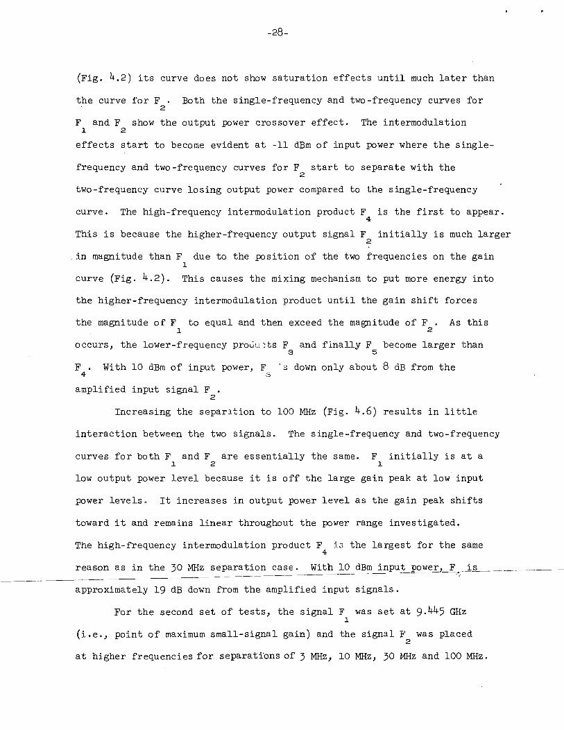
(Fig. -.2) its curve does not show saturation effects until much later than
the curve for F . Both the single-frequency and two-frequency curves for2
F and F show the output power crossover effect. The intermodulationi 2
effects start to become evident at -11 dBm of input power where the single-
frequency and two-frequency curves for F start to separate with the2
two-frequency curve losing output power compared to the single-frequency
curve. The high-frequency intermodulation product F is the first to appear.4
This is because the higher-frequency output signal F initially is much larger2
in magnitude than F due to the position of the two frequencies on the gaini
curve (Fig. -.2). This causes the mixing mechanism to put more energy into
the higher-frequency intermodulation product until the gain shift forces
the magnitude of F to equal and then exceed the magnitude of F . As thisi 2
occurs, the lower-frequency proouits F and finally F become larger than3 5
F . With 10 dBm of input power, F 's down only about 8 dB from the4 S
amplified input signal F .2
Increasing the separation to 100 MHz (Fig. .6) results in little
interaction between the two signals. The single-frequency and two-frequency
curves for both F and F are essentially the same. F initially is at a1 2 i
low output power level because it is off the large gain peak at low input
power levels. It increases in output power level as the gain peak shifts
toward it and remains linear throughout the power range investigated.
The high-frequency intermodulation product F is the largest for the same4
reason as in the 30 MHz separation case. With 10 dBm_3-nput_power,_F_^_J.^
approximately 19 dB down from the amplified input signals.
For the second set of tests, the signal F was set at 9. 5 GHzi
(i.e.. point of maximum small-signal gain) and the signal F was placed2
at higher frequencies for separations of 3 MHz, 10 MHz, JO MHz and 100 MHz.

-29-
SINGLE FREQUENCY
TWO FREQUENCY
-16 -12 -8 -4 0
INPUT POWER, dBm
8
FIG. ^.6 DYNAMIC CHARACTERISTICS OF AN IMPATT DIODE REFLECTION AMPLIFIER
FOR TWO EQUAL AMPLITUDE INPUT SIGNALS. (Af = 100 MHz)

-30-
The 3 MHz separation test had essentially the same behavior as that
illustrated in Fig. .3. The 10 MHz separation test (Fig. -7) resulted
in no output power crossover effect as F is always larger than F . Bothi 2
low-frequency intermodulation products F and F are larger than the high-3 5
frequency product F . These results are due to the gain peak shift and4
the consequent amplification increase at lower frequencies. The largest
intermodulation product F is 11 dB down from the original signals with3
10 dBm of input power.
The JO MHz (Fig. .8) and 100 MHz tests produced essentially the
same results. The single-frequency and two-frequency curves are approximately
the same for both F and F . The figures again show low-frequency dominancei 2
as F and F , the low-frequency intermodulation products, are always3 5
greater than the high-frequency intermodulation signal F .4
*<•,. 5 Conclusions. Small-signal, single-frequency gains in the
neighborhood of 30 dB are easily obtained in a double slug tuned coaxial
IMPATT diode reflection amplifier. With increasing RF input power the
single-frequency gain decreases, the point of maximum gain shifts to a
lower frequency and the bandwidth increases.
Operating the amplifier with two equal amplitude input signals
results in the generation of sum and difference frequency intermodulation
products. The shift in the maximum gain with increasing EF input power
provides a low-frequency dominance mechanism affecting both the amplified
source signals and the intermodulation_pro.duc-ts_. I.t_.i.s—possible—fe-r-the
low-frequency second-order intermodulation products to be greater in
magnitude than the high-frequency first-order intermodulation products,
depending on where the original signals are located relative to the

-31-
m
oUJ
oa.
O
SINGLE FREQUENCY
TWO FREQUENCY
-4 -
-8 -
-20 -16 -8 -4 0
INPUT POWER, dBm
8
FIG. Ji.T DYNAMIC CHARACTERISTICS OF AN IMPATT DIODE REFLECTION AMPLIFIER
FOR TWO EQUAL AMPLITUDE INPUT SIGNALS. (Af = 10 MHz)

-32-
ECD•o
UJ
OCL
CLH
O
DIODE-SiI0 = 40 mA
SINGLE FREQUENCY
TWO FREQUENCY
F, = 9.445
/ F2= 9.475 \ /
F"9.415
-8 -
-20 -12 -8 -4 0
INPUT POWER, dBm
8
FIG. 4.8 DYNAMIC CHARACTERISTICS OF AN IMPATT DIODE REFLECTION AMPLIFIER
FOR TWO EQUAL AMPLITUDE INPUT SIGNALS. (Af = JO MHz)

-33-
amplifier gain characteristics. As the frequency separation between the
two original signals is increased the interaction between the signals
(in terms of the output power generated at the source frequencies and
intermodulation products) is decreased.
k.6 Program for the Next Period. Intermodulation tests will be
conducted for several different frequencies in X-band. The tests will be
extended to input power levels large enough to reduce the maximum gain to
approximately 3 dB in order to investigate the limiting behavior of the
amplifier. These tests will also be conducted on GaAs diodes as soon as
appropriate devices are obtained.
_5 • Harmonic Generation Using Read Diode Varactors
Supervisor: G. I. Haddad
Staff; K. K- Dutta Choudhury
5'.1 Introduction. The mathematical formulation of the C-V
characteristic of the Read diode and its possible application as a
harmonic generator were presented in the previous report. The theoretical
small- and large-signal second-harmonic conversion efficiency and
normalized power output of a certain assumed realizable model of a
Read diode varactor are presented here. For comparison, the small- and .
large-signal second-harmonic conversion efficiency and normalized power
output of certain kinds of commercially available punch-through varactors
are also evaluated. The agreement between the large-signal varactor
analysis and the results obtained by Grayzel1 is excellent.
1. Grayzel, A. I., "Design Parameters for Overdriven Varactor FrequencyDoublers Using Punch-Through or Bimode Varactors," IEEE Trans. onMicrowave Theory and Techniques (Correspondence), vol. IT, No. 57PP. 3 5-3 7, June 1969.
It is worth mentioning that the mathematical formulation of the
Read diode varactor problem can be utilized for studying varactors haying
different types of C-V characteristics by modifying certain parameter values,
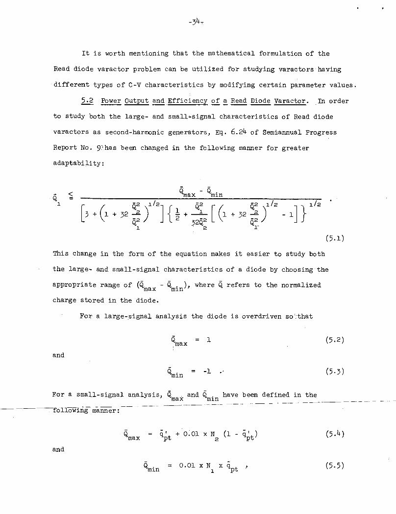
5.2 Power Output and Efficiency of a Read Diode Varactor. In order
to study both the large- and small-signal characteristics of Read diode
varactors as second-harmonic generators, Eq. 6.2k of Semiannual Progress
Report No. 9:'.has been changed in the following manner for greater
adaptability:
5 < Tnax min1 r / Q2 x1/2-! r Q2 r / O2 x1/2 -i > 1/'2
5 +r1 + 32S) /i + rr1 + 52i .x
(5.1)
This change in the form of the equation makes it easier to study both
the large- and small-signal characteristics of a diode by choosing the
appropriate range of (Q. - Q . ), where Q refers to the normalizedmax min
charge stored in the diode.
For a large-signal analysis the diode is overdriven so';that
%ax = X . .2)
and
Snin = -1 " (5-3)
F.or a small-signal analysis, Q . and Q . have been defined in the
following manner:
and
Q = q' + 0.01 x N (1 - q' ) (5-M^ ^pt 2 Pt' v '
Vn = 0.01 XNX xq p t , (5.5)

-35-
where q , and q' refer to the normalized charges at the normalized breakingpi/ PU
voltages v , and v' of the C-V characteristic. N and N values fix thep t p t 2 1
region of the C-V characteristic where the diode is allowed to operate.
In particular, N =0 and N = 100 correspond to a fully driven diode,i 2
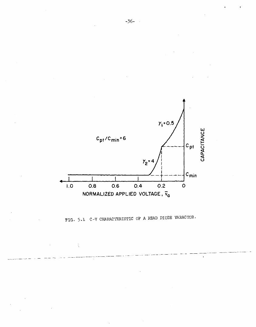
The models shown in Figs. 5-1 and 5-2 have been taken for studying
the conversion characteristics of a Read diode and a punch-through varactor,
respectively. The pertinent results of the large-signal analysis of these
two models are tabulated in Table 5-1; where v , = the normalized punch-pt
through voltage, v' = the normalized voltage beyond which capacitance remainspt
constant at C . , 7 = the exponents of capacitance variation in Regions Imin 1,2and II, respectively, as indicated in Figs. 5-1 and 5.2 and CD = 1/C . Rc cniri s
is the cutoff frequency of the diode.
Table 5-1
Tabulation of Large-Signal Normalized Power Output and Efficiency of Read
Diode and Punch-Through Varactors
(7 =0.5, v =0.2,
7 V '2 pt
4.o o.3
0 0.2
0.1 1.0
0.2 1.0
Normalized .PowerOutput (P)
0.13750
0.07293*
0.07880*
0.08520*
EfficiencyEff
84.718
94.653*
94.069*
93.393*
* 1The results agree with those of Grayzel.
The small-signal efficiency and normalized power output of the Read
diode model of Fig. 5-1 are presented in Figs. 5-3 and 5•4, respectively.
The same quantities for the diode of Fig. 5-2 are presented in Figs. 5-5
and 5-6, respectively.
-36-
cpt/cmirr6
I I
y,=o.5UJo
. I•p, u
<u
'mm
1.0 0.8 0.6 0.4 0.2
NORMALIZED APPLIED VOLTAGE, va
FIG. 5.1 C-V CHARACTERISTIC OF A READ DIODE VARACTOR.

-37-
V°
I I1.0 0.8 0.6 0.4 0.2 0
NORMALIZED APPLIED VOLTAGE, va
o
o
o
FIG. 5.2 C-V CHARACTERISTIC OF AN IDEAL PUNCH-THROUGH VARACTOR.

-38-
oo
I
P
OJ»
ofl
O
II
co
I
rH O< rH
E-!
M
II
4°-P
R-

-39-
K>O
X
Q. 40 —13O
ccliJ$OQ.OLJN
a:O
10 —
FIG. THEORETICAL NORMALIZED POWER OUTPUT OF THE READ DIODE VARACTOR
OF FIG. 5-1 FOR DIFFERENT N AND N VALUES. (y = 0-5, 7 = ^,1 2 3 . 2

100-IK)-
\ \ \\\ \ \Nof\ \ cr\ \ A r\ » on\80 \60\40 \20 \0K) \60\40 \20 \0
\\ \ \ \\ x v \\\\ \ •\\ \ \
\ \ ' x - \\.\\ \^ V\\ \ \v \ \ \\\ \
\\\ \x V I\\\\ \
0 10 20 30 40 50 60 70 80 90 100
NlFIG. 5.5 THEORETICAL EFFICIENCY OF THE VARACTOR OF FIG. 5.2 FOR DIFFERENT
N AND N VALUES. (y = 0.5, 7 = 0. v , = 0.2. vV - 0.2,i 2 i o Pt Pt '

FIG. 5.6 THEORETICAL NORMALIZED POWER OUTPUT OF THE VARACTOR OF FIG. 5-2
FOR DIFFERENT N AND N VALUES. (y = 0.5, J = 0, v , = 0.2,1 2 i 2 P t
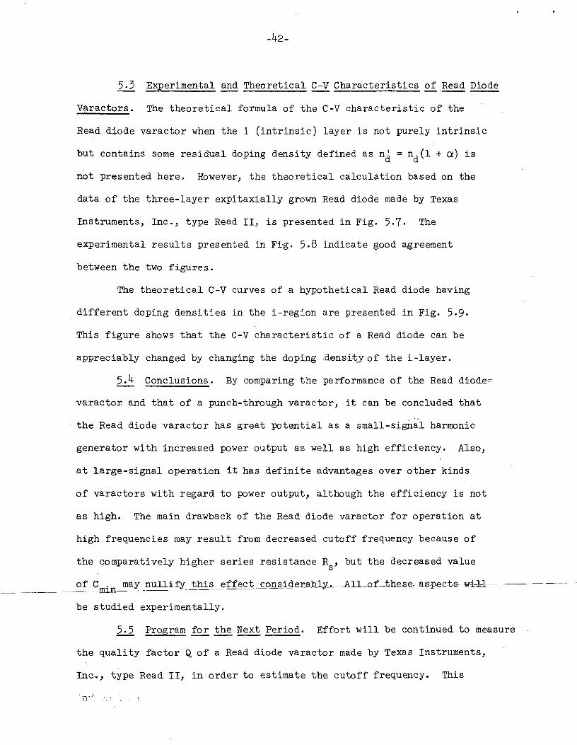
5-3 Experimental and Theoretical C-V Characteristics of Read Diode
Varactors. The theoretical formula of the C-V characteristic of the
Read diode varactor when the i (intrinsic) layer is not purely intrinsic
but contains some residual doping density defined as n' = n,(1 + a) is
not presented here. However, the theoretical calculation based on the
data of the three-layer expitaxially grown Read diode made by Texas
Instruments, Inc., type Read II, is presented in Fig. 5-7- The
experimental results presented in Fig. 5-8 indicate good agreement
between the two figures.
The theoretical C-V curves of a hypothetical Read diode having
different doping densities in the i-region are presented in Fig. 5-9-
This figure shows that the C-V characteristic of a Read diode can be
appreciably changed by changing the doping density of the i-layer.
5-A Conclusions. By comparing the performance of the Read diode-
varactor and that of a punch-through varactor, it can be concluded that
the Read diode varactor has great potential as a small-signal harmonic
generator with increased power output as well as high efficiency. Also,
at large-signal operation it has definite advantages over other kinds
of varactors with regard to power output, although the efficiency is not
as high. The main drawback of the Read diode varactor for operation at
high frequencies may result from decreased cutoff frequency because of
the comparatively higher series resistance R , but the decreased values
of C . may nullify this effecjt_conAiAe_rably-—All_o.f—the.se-as-pec-ts-:-w-i-l-l-
be studied experimentally.
5.5 Program for the Next Period. Effort will be continued to measure
the quality factor Q of a Read diode varactor made by Texas Instruments,
Inc., type Read II, in order to estimate the cutoff frequency. This

10
6
4
u. 2o.
uToI .I 0.6o
0.4
0.2
O.I
TI READ DIODE TYPE I
4 6 10
, V
20 40 60 100
'B
FIG. 5-7 THEORETICAL C-V CURVE OF THE TI READ DIODE.

-kk-
10
6
4
LJO
|OI J
i T
U0.6
0.4
0.2
O.I
TI READ DIODE TYPE H
4 6 10
, V
20 40 60 100
B
FIG. 5.8 EXPERIMENTAL C-V CURVE OF THE TI READ DIODE.

-45-
nj nd nd(H-a) nj
p+
.
nli
n2
— *2-*
n+
MATERIAL: si
nJ = IOl8cm'3
n = IOl6cm"3
-0.5. -0.8
4 1,60A
150
140
130
120
110
30X10-5
CM
20
10
0
'B
UJIT
HZO
UJo
1oQ.
O
BIAS
FIG. 5-9 THEORETICAL C-V CURVE OF A READ DIODE WITH DIFFERENT DOPING
DENSITY IN THE i-LAYER.

information will be used to design a second-harmonic converter to determine
how the theoretically predicted power output and efficiency agree with the
experimental results.
6. Fabrication of Schottky-Barrier IMPATT Diodes
Supervisors: G. I. Haddad and S. N. Shabde
Staff: S. P. Kwok
6.1 Introduction. It was shown theoretically1 that the effective
avalanche width of a Si IMPATT diode using an n pp structure is smaller
than the corresponding complementary p nn one. However, the problem of
minority carrier storage2 becomes increasingly more significant in a diode
with a narrow avalanche region. A Schottky-barrier IMPATT diode using
p-type Si could have the advantage of a narrow avalanche region without
the minority carrier storage problem. During this period titanium (Ti) was
used for the fabrication of Schottky barriers on a p-type Si wafer and
the barrier height was determined. Meanwhile, the fabrication of a
PtSi-Si(n) Schottky barrier also progressed considerably.
6.2 Ti-Si(p) Schottky Barrier.
6.2.1 Fabrication. A pp Si wafer with a 2 n-cm and 3-5 |-im
thick epitaxial layer is first chemically thinned on the substrate side
to approximately 0.001 inch. The wafer is then cleaned in TCE, acetone,
Freon, HF and DI water. It is then prebaked in vacuum at 300°C for one-
half hour and is allowed to cool for the same period. Then Ti (250 A"),
1. Schroeder, W. E. and Haddad, G. I., "Avalanche Region Width in VariousStructures of IMPATT Diodes," Proc. IEEE (Correspondence), vol. 59,No. 8, pp. 1245-1248, August 1971.
2. Misawa, T., "Minority Carrier Storage and Oscillation Efficiency inRead Diodes," Solid-State Electronics, vol. 13, No. 10, pp. 1369-1374,October 1970.

Cr (250 A) and Au (0.5 i-itn) are sequentially evaporated on the epitaxial
layer. Cr and Au layers of the same thickness are used for making ohmic
contact on the substrate side. Using the usual photolithographic technique
diodes are formed and separated. To avoid sharp curvature in the junction
due to undercutting during the etching process, the etching was done from
the substrate side. A mixture of HNO and HF (95$: 5$) was found to be a3
mild enough etchant so as' not to cause a severe undercutting of the TI layer
during Si etching. After the diodes have been separated they are ready
for measurement .
6.2.2 Height of Ti-Si(p) Schottky Barrier. The I-V character-
istic of a typical diode is shown in Fig. 6.1 and its C-V characteristics,
in Fig. 6.2. The rise in capacitance value at high voltages is due to the
high reverse saturation current. The slope of 1/C2 vs. voltage is
constant at low voltages up to approximately ~5 V. From the slope the
acceptor impurity density of 7-^ x 10l5/cm3 was obtained which corresponds
to the specified resistivity of 2 fi-cm. The height of the barrier was
determined from the zero -volt intercept of the extrapolated forward current.
The barrier height cp is given by the following equation:3Bp
where k = the Boltzmann constant,
T = the temperature,
q = the electronic charge,
J = the zero-volt current intercept or the saturation current ands**
A = the Richardson constant.
Sze, S. M., Physics of Semiconductor Devices, John Wiley and Sons., Inc.,' New York, Chap. 8, 1969.

-48-
10,-20 10
VOLTAGE, V
20 30 40 50
ID'3 -
UJQl
o
DIAMETER = 0.015 INCHNA=74xlO l5/cm3
io-8
10-9 I I
0 O.I
60
0.2 0.3 0.4 0.5
VOLTAGE, V
FIG. 6.1 I-V CHARACTERISTICS OF THE Ti-Si(p) SCHOTTKY BARRIER.
0.6

>UJo
o
O
CO
p
coM
TS
M

-50-
The Richardson constant is taken to be 32 A/cm2/°K2 for holes.3 This
procedure yields cp = 0.58 V. The barrier height is calculated to beBp
<p_ = 0.56 V from the reverse current value at 1 V » kT/q and theup
following expression:
where Acp is the barrier lowering due to the image force, which is
Aep = , (6.3)
E is the maximum value of the electric field and e is the dielectric
constant of the semiconductor.
On the other hand, the barrier height is related to the intercept
of the 1/C2 line on the voltage axis, which is V., as
= vi+ vp -Acp + -where
N is the well-known effective density of states in the valence band
and N. is the acceptor impurity density taken to be 7-^ x 10l5/cm3. Ther\
resultant 9_ is 0.6o V. Therefore it is concluded that the height ofBp
the Ti-Si(p) Schottky barrier is
co = 0.58 ± 0.02 VBp

-51-
This value is higher than the highest barrier height of ZrSi (0.53-0-55 V)
reported recently.4
6.3 PtSi-Si(n) Schottky Barrier. A fabrication procedure for a
PtSi-Si(n) barrier utilizing this laboratory's sputtering system has been
established which yields good reverse breakdown characteristics as shown
in Fig. 6.3. The figure shows a diode with background doping of 10l6/cm3,
an epitaxial layer width of 3-5 um and a breakdown of 65 V as expected
theoretically. The basic steps of the fabrication are as follows:
1. Backsputter the wafer.
2. Heat the sputtering source and its surroundings for a few minutes
and cool it by lowering the dc sputtering current. This step reduces the
outgassing of the impurities during the subsequent sputtering.
3- Sputter Pt at a suitable rate of deposition.
**•• Sinter the wafer in vacuum at approximately 650°C for 5 to 10
minutes to form a platinum silicide interface.
5- Evaporate Cr and Au for ohmic contacts.
6. Separate the diodes. This may involve an additional etching of a
thin Pt layer which remains there after sintering: this is done by using
hot H SO (150°C) or aqua regia.
6. _ Conclusions and Program for the Next ; Period. The barrier height
of Ti-Si(p) reported here was higher than the highest value of ZrSi (p)2
reported elsewhere.4 However, a Schottky-barrier height of 0.5 V is
still low for the application of IMPATT oscillators due to the inherent
large reverse saturation current and its thermal instability. Most
recently, hafnium-Si(p) Schottky barriers have been reported5 to have a
4. Andrews, J. M. and Lepselter, M. P., "Metal-Silicide Schottky Diodes,"Solid-State Electronics,. vol. 13, No. 1, .pp. 1011-1023, July 1970.
5. Saxena, A. R., "Hafnium-Si Schottky Barriers: Large Barrier Heighton p-Type Si and Ohmic Behavior on n-Type Si," Appl. Phys. Letters,vol. 19, No. 3, pp. 71-73, 1 August 1971.

-52-
20 V/DIVISION
NA=IOl6/cm3
EIG- 6.J BREAKDOWN CHARACTERISTIC OF A PtSi-Si(n) SCHOTTKY BARRIER.

-55-
height of 0.9 eV. The fabrication of an IMPATT diode using such a barrier
will be pursued during the next period.
With the fabrication procedure of a PtSi^-SiCn) -barrier1 already
successfully established, it is expected that X-band Schottky-barrier
oscillators will be fabricated during the next period.


![Chapter 1: Diode circuits vtusolutionvtusolution.in/uploads/9/9/9/3/99939970/analog_electronic[15ec32].pdf · Chapter 1: Diode circuits ... • Diode testing • Zener diode • Diode](https://img.dokumen.tips/doc/110x75/5aedefea7f8b9a9031905d54/chapter-1-diode-circuits-vt-15ec32pdfchapter-1-diode-circuits-diode.jpg)