Embed Size (px)
Citation preview

A Study of Photoactive Materials for Solution-Processed Thin-Film Solar Cells
by
Andrew Namespetra
Submitted in partial fulfilment of the requirements
for the degree of Master of Science
at
Dalhousie University
Halifax, Nova Scotia
August 2015
© Copyright by Andrew Namespetra, 2015

ii
DEDICATIONS
I dedicate this thesis to my family, for their love and support, and to all of my friends who
have accompanied me on the journey through grad school.

iii
TABLE OF CONTENTS
List of Tables ................................................................................................................ vi
List of Figures ................................................................................................................ vii
Abstract ......................................................................................................................... xi
List of Abbreviations Used ........................................................................................... xii
Acknowledgments ......................................................................................................... xiv
Chapter 1: Introduction ................................................................................................. 1
1.1 Background: Solar Photovoltaic Technologies ............................................. 1
1.2 Perovskite Solar Cells (PSCs) ....................................................................... 2
1.2.1 Perovskite Materials ......................................................................... 2
1.2.2 Photovoltaic Mechanism in Perovskite Solar Cells .......................... 3
1.2.3 Perovskite Solar Cell Device Construction ....................................... 5
1.3 Organic Solar Cells ........................................................................................ 6
1.3.1 Organic Semiconductor Materials...................................................... 6
1.3.2 Photovoltaic Mechanism in Organic Solar Cells .............................. 7
1.3.3 Organic Solar Cell Device Construction ........................................... 8
1.4 Solar Cell Device Testing and Performance Metrics .................................... 9
1.5 Thin Film Formation for Solar Cell Applications ......................................... 13
1.6 Project Goals ................................................................................................. 15
Chapter 2 – Characterization Techniques ..................................................................... 16
2.1 Optical Microscopy (OM) .............................................................................. 16
2.2 Scanning Electron Microscopy (SEM) .......................................................... 16
2.3 Atomic Force Microscopy (AFM) ................................................................. 16
2.4 X-ray Diffraction (XRD) ............................................................................... 19
2.5 UV-Visible (UV-Vis) Spectroscopy .............................................................. 20
2.6 Photoluminescence (PL) Spectroscopy ......................................................... 20
2.7 Cyclic Voltammetry (CV) ............................................................................. 21
Chapter 3: Thin Film Formation in Perovskite Solar Cells ........................................... 23
3.1 Background .................................................................................................... 23
3.1.1 Solution-Processed Perovskite Solar Cells ....................................... 23
3.1.2 Active Layer Components and Device Architecture ......................... 23

iv
3.1.3 Methods of Solution-Processed Perovskite Thin Films .................... 24
3.2 Experimental Methods – Sequential Dip Coating ......................................... 26
3.2.1 PbI2 and MAPbI3 Thin Films ............................................................. 26
3.2.2 Perovskite Solar Cell Fabrication Using Sequential Dip Coating .... 28
3.3 Perovskite Solar Cell Device Characterization ............................................. 29
3.4 Results and Discussion – Sequential Dip Coating ........................................ 30
3.4.1 Solution Concentration (Csolution) and Spin Speed .............................. 31
3.4.2 Substrate Temperature (Tsubstrate) ....................................................... 33
3.4.3 Device Performance Using Sequential Dip Coating ......................... 35
3.5 Experimental Methods – Sequential Spin Coating ........................................ 37
3.6 Results and Discussion – Sequential Spin Coating ....................................... 38
3.6.1 Annealing Conditions ....................................................................... 38
3.6.2 MAI Concentration ........................................................................... 40
3.6.3 Device Performance Using Sequential Spin Coating ....................... 42
3.7 Conclusions ................................................................................................... 43
Chapter 4: Organic Hole-Transporting Materials for Perovskite Solar Cells ............... 45
4.1 Background .................................................................................................... 45
4.2 Materials and Methods .................................................................................. 47
4.2.1 Materials ............................................................................................ 47
4.2.2 Thin Film Formation via Spin-Coating ............................................. 49
4.2.3 Perovskite Solar Cell Fabrication Procedure .................................... 50
4.3 Results and Discussion .................................................................................. 51
4.3.1 Materials Characterization ................................................................ 51
4.3.2 Perovskite Solar Cell Fabrication and Testing .................................. 55
4.3.3 Hole-Transporting Layer Surface Morphology ................................ 56
4.4 Conclusions ................................................................................................... 58
4.5 Future Work .................................................................................................... 60
Chapter 5: Star-Shaped Donor Materials for Small-Molecule Organic Solar Cells .... 62
5.1 Background .................................................................................................... 62
5.1.1. Transition from Hole-Transporting Materials to Donors ................. 62
5.1.2 Selection of a Complementary Acceptor .......................................... 62

v
5.1.3 Custom-Made Donor-Acceptor Pairs ................................................ 64
5.2 Materials and Methods .................................................................................. 65
5.2.1 Materials ............................................................................................ 65
5.2.2 Thin-Film Formation via Spin Coating ............................................. 67
5.2.3 Organic Solar Cell Fabrication Procedure ........................................ 68
5.2.4 Organic Solar Cell Testing ................................................................ 69
5.3 Results and Discussion, Part I ....................................................................... 69
5.3.1 Materials Characterization, Part I ..................................................... 69
5.3.2 Thin-Film Characterization, Part I .................................................... 72
5.3.3 Organic Solar Cell Testing, Part I ..................................................... 77
5.3.4 Conclusions, Part I ............................................................................ 79
5.4 Results and Discussion, Part II ...................................................................... 80
5.4.1 New Acceptors: A Molecular Design Strategy ................................. 80
5.4.2 Materials Characterization, Part II .................................................... 82
5.4.3 Thin-Film Characterization, Part II .................................................... 83
5.4.4 Organic Solar Cell Testing, Part II .................................................... 88
5.4.5 Conclusions, Part II ........................................................................... 88
5.5 Outlook and Future Work .............................................................................. 89
Chapter 6 – Conclusions ............................................................................................... 92
References ..................................................................................................................... 95
Appendix A – Solution Preparations ............................................................................ 104
Appendix B – Synthesis of CH3NH3I ............................................................................ 106
Appendix C – Other Factors Influencing Lead Iodide Film Morphology .................... 107
Appendix D – Perovskite X-ray Diffraction Peak Intensities ....................................... 109
Appendix E – Thiophene in Organic Small Molecules ................................................ 110
Appendix F – The Effect of Dopants on Hole-transport ............................................... 113
Appendix G – The Effect of Non-conjugated Polymer Additives on Film
Formation of Hole-transport Layers ............................................................................. 114
Appendix H – 3D Non-Fullerene Acceptors ................................................................. 117
Appendix I – Varying Donor-Acceptor Ratios ............................................................. 119
Appendix J – Solvent Additives and Solvent Vapour Annealing ................................. 121
vi
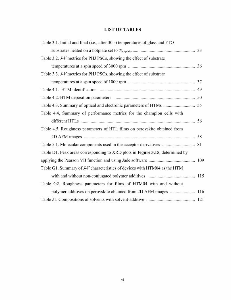
LIST OF TABLES
Table 3.1. Initial and final (i.e., after 30 s) temperatures of glass and FTO
substrates heated on a hotplate set to Thotplate. ....................................................... 33
Table 3.2. J-V metrics for PHJ PSCs, showing the effect of substrate
temperatures at a spin speed of 3000 rpm ........................................................... 36
Table 3.3. J-V metrics for PHJ PSCs, showing the effect of substrate
temperatures at a spin speed of 1000 rpm ........................................................... 37
Table 4.1. HTM identification .................................................................................... 49
Table 4.2. HTM deposition parameters ........................................................................ 50
Table 4.3. Summary of optical and electronic parameters of HTMs ............................ 55
Table 4.4. Summary of performance metrics for the champion cells with
different HTLs ..................................................................................................... 56
Table 4.5. Roughness parameters of HTL films on perovskite obtained from
2D AFM images .................................................................................................. 58
Table 5.1. Molecular components used in the acceptor derivatives ............................. 81
Table D1. Peak areas corresponding to XRD plots in Figure 3.15, determined by
applying the Pearson VII function and using Jade software ......................................... 109
Table G1. Summary of J-V characteristics of devices with HTM04 as the HTM
with and without non-conjugated polymer additives .......................................... 115
Table G2. Roughness parameters for films of HTM04 with and without
polymer additives on perovskite obtained from 2D AFM images ...................... 116
Table J1. Compositions of solvents with solvent-additive ........................................... 121

vii
LIST OF FIGURES
Figure 1.1. CH3NH3PbI3 crystal structure ............................................................... 3
Figure 1.2. Energy level diagram and device architecture for a PSC ..................... 5
Figure 1.3. Examples of π-conjugated organic materials for OSCs ....................... 7
Figure 1.4. Energy level diagram and device architecture for an OSC ................... 8
Figure 1.5. Bulk and planar heterojunction active layers for OSCs ....................... 9
Figure 1.6. Illustrated I-V curves for a SC .............................................................. 10
Figure 1.7. Circuit diagrams for SCs operating under dark and light conditions .... 12
Figure 1.8. Illustrated I-V curves showing the detrimental effects on FF with
increasing RS and decreasing RSH .................................................................. 13
Figure 1.9. An illustration of the stages involved in the spin-casting procedure .... 14
Figure 2.1. An illustration of the operation of an AFM .......................................... 17
Figure 3.1. Device architectures for planar and mesostructured PSCs ................... 24
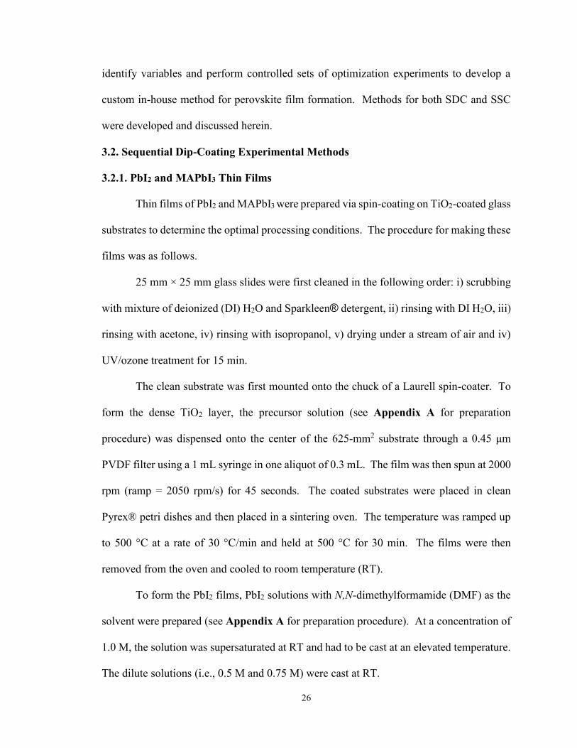
Figure 3.2. Photographs depicting the stages of the SDC procedure ...................... 28
Figure 3.3. A photograph of a substrate with 16 completed PSC devices .............. 30
Figure 3.4. OM images of PbI2 films spin-cast on TiO2 compact films showing
the effect of solution concentration and spin speed ....................................... 32
Figure 3.5. SEM images of the CH3NH3PbI3 films after conversion of the PbI2
films via SDC, showing the effect of solution concentration and spin
speed .............................................................................................................. 32
Figure 3.6. SEM images of PbI2 films spin-cast on TiO2 compact films and the
corresponding CH3NH3PbI3 films after conversion via dipping, showing
the effect of spin speed and substrate temperature ......................................... 34
Figure 3.7. SEM images of PbI2 films spin-cast on TiO2 compact films and the
corresponding CH3NH3PbI3 films after conversion via dipping, showing
the effect of substrate temperature ................................................................. 35
Figure 3.8. J-V curves for the best-performing PHJ PSCs with PbI2 films
deposited at 3000 rpm on substrates heated to different temperatures .......... 36
Figure 3.9. J-V characteristics of the best-performing PHJ PSCs with PbI2 films
deposited at 1000 rpm on substrates heated to different temperatures .......... 37
Figure 3.10. Photographs of films depicting stages of SSC procedure .................. 37
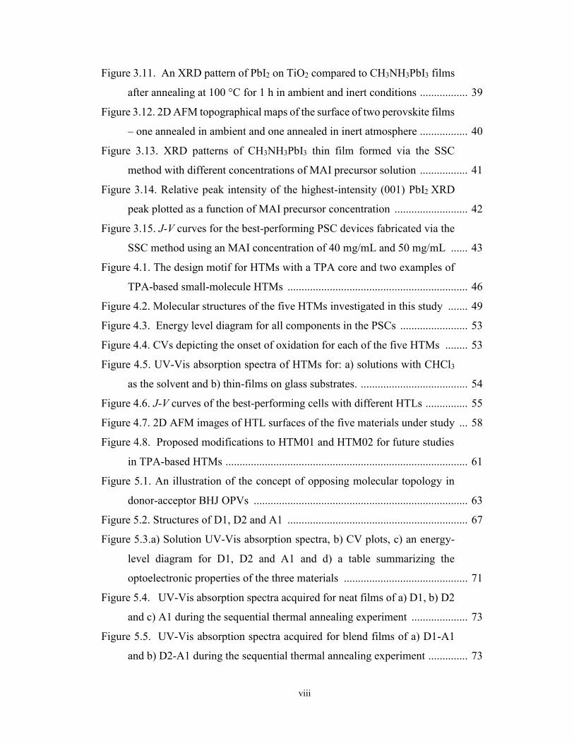
viii
Figure 3.11. An XRD pattern of PbI2 on TiO2 compared to CH3NH3PbI3 films
after annealing at 100 °C for 1 h in ambient and inert conditions ................. 39
Figure 3.12. 2D AFM topographical maps of the surface of two perovskite films
– one annealed in ambient and one annealed in inert atmosphere ................. 40
Figure 3.13. XRD patterns of CH3NH3PbI3 thin film formed via the SSC
method with different concentrations of MAI precursor solution ................. 41
Figure 3.14. Relative peak intensity of the highest-intensity (001) PbI2 XRD
peak plotted as a function of MAI precursor concentration .......................... 42
Figure 3.15. J-V curves for the best-performing PSC devices fabricated via the
SSC method using an MAI concentration of 40 mg/mL and 50 mg/mL ...... 43
Figure 4.1. The design motif for HTMs with a TPA core and two examples of
TPA-based small-molecule HTMs ................................................................ 46
Figure 4.2. Molecular structures of the five HTMs investigated in this study ....... 49
Figure 4.3. Energy level diagram for all components in the PSCs ........................ 53
Figure 4.4. CVs depicting the onset of oxidation for each of the five HTMs ........ 53
Figure 4.5. UV-Vis absorption spectra of HTMs for: a) solutions with CHCl3
as the solvent and b) thin-films on glass substrates. ...................................... 54
Figure 4.6. J-V curves of the best-performing cells with different HTLs ............... 55
Figure 4.7. 2D AFM images of HTL surfaces of the five materials under study ... 58
Figure 4.8. Proposed modifications to HTM01 and HTM02 for future studies
in TPA-based HTMs ...................................................................................... 61
Figure 5.1. An illustration of the concept of opposing molecular topology in
donor-acceptor BHJ OPVs ............................................................................ 63
Figure 5.2. Structures of D1, D2 and A1 ................................................................ 67
Figure 5.3.a) Solution UV-Vis absorption spectra, b) CV plots, c) an energy-
level diagram for D1, D2 and A1 and d) a table summarizing the
optoelectronic properties of the three materials ............................................ 71
Figure 5.4. UV-Vis absorption spectra acquired for neat films of a) D1, b) D2
and c) A1 during the sequential thermal annealing experiment .................... 73
Figure 5.5. UV-Vis absorption spectra acquired for blend films of a) D1-A1
and b) D2-A1 during the sequential thermal annealing experiment .............. 73

ix
Figure 5.6. PL spectra comparing as-cast neat and blend films .............................. 75
Figure 5.7. XRD patterns one-component thin-films of a) D1 and b) A1 and c)
a two-component blend film acquired before and after thermal annealing
........................................................................................................................ 76
Figure 5.8. XRD patterns of separate films of D1-A1 blends (1:1 weight ratio)
comparing the effect on crystallinity of annealing temperature .................... 77
Figure 5.9. a) J-V curves of representative devices with D1-A1 active-layer
blends in a 1:1 ratio. b) An illustration of the layered “conventional”-
style architecture. c) A table of performance metrics. d) Photographs of
the completed devices .................................................................................. 78
Figure 5.10. AFM images of the D1:A1 active-layer surfaces of the devices ........ 79
Figure 5.11. Structures of A1 and the four new derivatives ................................... 81
Figure 5.12. a) Energy level diagram of the frontier molecular orbitals of D1
and the five acceptors determined by CV. b) CV plots for the acceptor
derivatives, normalized such that the current of the first oxidation peak
is set to unity .................................................................................................. 82
Figure 5.13. Thin-film characterization of D1:Ax blended films (1:1 by-weight)
as-cast (dashed lines) and after thermally annealing at 180 °C for 10 min
(solid lines). UV-Vis absorption spectra (a-e) and XRD patterns (g-k) are
shown in the left- and right-hand columns, respectively ............................... 85
Figure 5.14. 2D AFM topographical images of the surfaces of thin-film blends
of A1 with acceptors A2, A3, A4 and A5, as-cast and after annealing at
180 °C for 10 min .......................................................................................... 87
Figure 5.15. A comparison of the structures of A2 and AX ................................... 91
Figure C1. SEM images of PbI2 films spin-cast on TiO2 compact films and the
corresponding CH3NH3PbI3 films after conversion via dipping, showing
the effect of solution temperature .................................................................. 107
Figure C2. SEM images of PbI2 films spin-cast on TiO2 compact films and the
corresponding CH3NH3PbI3 films after conversion via dipping, showing
the effect of different atmospheres ................................................................ 108

x
Figure E1. Structures of small-molecule HTMs for PSCs with thiophene
functionalities ................................................................................................ 111
Figure E2. Structures of polymer HTMs for PSCs with thiophene
functionalities ................................................................................................ 112
Figure F1. A comparison of J-V curves of the best-performing devices with
Spiro-OMeTAD doped with Li-TFSI and tBP against devices undoped
Spiro-OMeTAD ............................................................................................. 113
Figure G1. A comparison J-V curves for the best-performing devices with
HTM04 with and without non-conjugated polymer additives ....................... 114
Figure G2. 2D AFM images of HTL surfaces of HTM04 with and without
polymer additives on a perovskite film ......................................................... 115
Figure H1. Examples of 3D non-fullerene acceptors .............................................. 118
Figure I1. UV-Vis absorption spectra acquired for as-cast blend films of a) D1-
A1 and b) D2-A1 with varying D:A weight ratios ........................................ 119
Figure I2. XRD patterns of thin-film blends with D1-A1 ratios of a) 1:1 and b)
1:2 acquired before and after thermal annealing ........................................... 120
Figure J1. UV-Vis spectra of D1-A1 blend thin films (1:1 weight ratio) with
various amounts of solvent additives ............................................................ 122
Figure J2. A photograph of a D1-A1 thin film undergoing SVA in an annealing
chamber ......................................................................................................... 123
Figure J3. a) UV-Vis spectra of a D1-A1 blend thin film (1:1 weight ratio)
before and after sequential SVA. b) XRD patterns of a D1-A1 blend thin
film before and after SVA for 20 min ........................................................... 124
xi
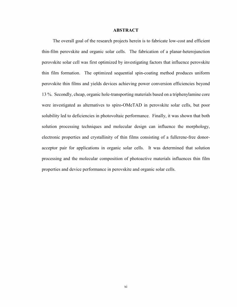
ABSTRACT
The overall goal of the research projects herein is to fabricate low-cost and efficient
thin-film perovskite and organic solar cells. The fabrication of a planar-heterojunction
perovskite solar cell was first optimized by investigating factors that influence perovskite
thin film formation. The optimized sequential spin-coating method produces uniform
perovskite thin films and yields devices achieving power conversion efficiencies beyond
13 %. Secondly, cheap, organic hole-transporting materials based on a triphenylamine core
were investigated as alternatives to spiro-OMeTAD in perovskite solar cells, but poor
solubility led to deficiencies in photovoltaic performance. Finally, it was shown that both
solution processing techniques and molecular design can influence the morphology,
electronic properties and crystallinity of thin films consisting of a fullerene-free donor-
acceptor pair for applications in organic solar cells. It was determined that solution
processing and the molecular composition of photoactive materials influences thin film
properties and device performance in perovskite and organic solar cells.
xii
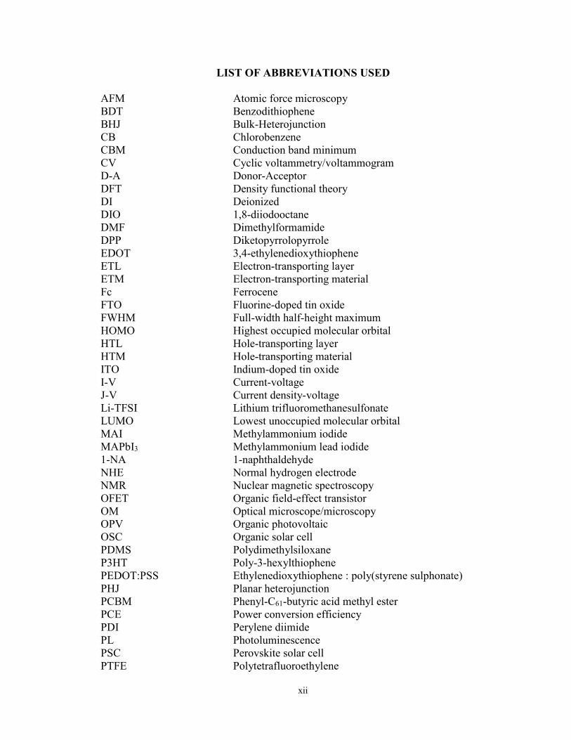
LIST OF ABBREVIATIONS USED
AFM Atomic force microscopy
BDT Benzodithiophene
BHJ Bulk-Heterojunction
CB Chlorobenzene
CBM Conduction band minimum
CV Cyclic voltammetry/voltammogram
D-A Donor-Acceptor
DFT Density functional theory
DI Deionized
DIO 1,8-diiodooctane
DMF Dimethylformamide
DPP Diketopyrrolopyrrole
EDOT 3,4-ethylenedioxythiophene
ETL Electron-transporting layer
ETM Electron-transporting material
Fc Ferrocene
FTO Fluorine-doped tin oxide
FWHM Full-width half-height maximum
HOMO Highest occupied molecular orbital
HTL Hole-transporting layer
HTM Hole-transporting material
ITO Indium-doped tin oxide
I-V Current-voltage
J-V Current density-voltage
Li-TFSI Lithium trifluoromethanesulfonate
LUMO Lowest unoccupied molecular orbital
MAI Methylammonium iodide
MAPbI3 Methylammonium lead iodide
1-NA 1-naphthaldehyde
NHE Normal hydrogen electrode
NMR Nuclear magnetic spectroscopy
OFET Organic field-effect transistor
OM Optical microscope/microscopy
OPV Organic photovoltaic
OSC Organic solar cell
PDMS Polydimethylsiloxane
P3HT Poly-3-hexylthiophene
PEDOT:PSS Ethylenedioxythiophene : poly(styrene sulphonate)
PHJ Planar heterojunction
PCBM Phenyl-C61-butyric acid methyl ester
PCE Power conversion efficiency
PDI Perylene diimide
PL Photoluminescence
PSC Perovskite solar cell
PTFE Polytetrafluoroethylene

xiii
PVDF Polyvinylidene fluoride
R2R Roll-to-roll
RMS Root mean square
RT Room temperature
SDC Sequential dip-coating
SEM Scanning electron microscopy
SPM Scanning probe microscopy
SSC Sequential spin-coating
SVA Solvent vapour annealing
tBP tert-butylpyridine
4-TFBA 4-trifluoromethyl benzoic acid
TGA Thermogravimetric analysis
TFT Thin-film transistor
THF Tetrahydrofuran
TPA Triphenylamine
UPS Ultraviolet photoelectron spectroscopy
UV-Vis Ultraviolet-Visible
VBM Valence band maximum
XPS X-ray photoelectron spectroscopy
XRD X-ray diffraction

xiv
ACKNOWLEDGEMENTS
First and foremost, I would like to thank my supervisors Prof. Gregory Welch and Prof. Ian
Hill for their continued guidance and mentorship throughout my program. I also
thank Prof. Jean Burnell for his assistance on my thesis and Prof. Mary Anne White
and Prof. Jeffery Dahn for their roles as committee members.
This work was made possible due to collaborations with other members of the Welch and
Hill research groups. I would like to thank each contributing member individually:
i) Arthur Hendsbee for: i) synthesis of organic materials including D1 and A1-A5,
HTM01 and HTM02, ii) acquisition of CV data for D1, A1, A3, A4 and A5, iii)
XRD patterns of the thermally-annealed blend films of D1:A1;
ii) Elizabeth Kitching for: i) spin-coating of the D1:A1 1:1 blends, ii) thermal-
annealing of the corresponding films, and iii) acquisition of UV-Vis spectra of
the films;
iii) Jetsuda Areephong for: i) synthesis of HTM03 and DPP1 and ii) acquisition of
the corresponding solution UV-Vis and CV data for each of these materials;
iv) Seth McAfee for running the CV experiments for HTM04;
v) Jess Topple for her guidance and advice on use of the AFM; and
vi) Charlotte Clegg for help and support with optimizations of perovskite thin-
films.
I wish to thank Dalhousie faculty members: Prof. Mark Obrovac for the use of his X-ray
diffractometer and Prof. Jeff Dahn for the use of his SEM.
I would also like to thank Dr. Nicholas Vukotic for helping me with the analysis of the
XRD powder patterns in Figure 3.15 using Jade software.
1
CHAPTER 1 - INTRODUCTION
1.1 Background: Solar Photovoltaic Technology
As the global demand for energy is projected to rise over the next few decades,1
clean, renewable sources of energy are becoming increasingly important. Energy-capture
systems such as wind, solar and hydroelectric are important to offset the dependence on
fossil fuels for energy conversion.
Solar energy is particularly promising given the vast resource provided by the Sun.
For example, 4.3×10²⁰ J of energy from the Sun strikes the Earth every hour, which greatly
exceeds the amount of energy consumed in the United States in an entire year.2,3 Other
strategies exist to capture energy from the Sun (e.g., solar thermal, solar fuels, etc.), but
solar photovoltaic (PV) technology is the conversion of solar energy directly into
electricity.
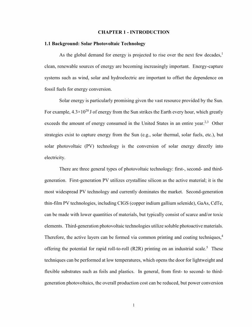
There are three general types of photovoltaic technology: first-, second- and third-
generation. First-generation PV utilizes crystalline silicon as the active material; it is the
most widespread PV technology and currently dominates the market. Second-generation
thin-film PV technologies, including CIGS (copper indium gallium selenide), GaAs, CdTe,
can be made with lower quantities of materials, but typically consist of scarce and/or toxic
elements. Third-generation photovoltaic technologies utilize soluble photoactive materials.
Therefore, the active layers can be formed via common printing and coating techniques,4
offering the potential for rapid roll-to-roll (R2R) printing on an industrial scale.5 These
techniques can be performed at low temperatures, which opens the door for lightweight and
flexible substrates such as foils and plastics. In general, from first- to second- to third-
generation photovoltaics, the overall production cost can be reduced, but power conversion
2
efficiencies (PCEs) also decrease. It is therefore a challenge to increase the PCE of third-
generation PV to realize low-cost and efficient solar cells.
Two promising third-generation PV technologies are perovskite solar cells (PSCs)
and organic solar cells (OSCs). PSCs have rapidly gained attention in the scientific
community since their discovery in 2009.6 To date, the most efficient lab-scale perovskite
solar cells deliver a PCE greater than 19 %.7 Although these were small area (10 mm2)
devices, they have the potential to compete with multi-crystalline Si solar cells, which
demonstrate PCEs of ca. 21 % in larger-area modules.8
Organic solar cells employ organic π-conjugated polymers or small molecules as
light-harvesters. While less efficient than PSCs and other inorganic photovoltaic
technologies, OSCs have also seen great improvements in efficiency over the past three
decades. Since one of the first reports of a functional organic solar cell in 1986 by Tang,9
the efficiency of devices has improved from under 1% to the record of 11% in 2015.8
Despite similarities in operating principles, perovskite and organic solar cells have
significant differences. Therefore, a discussion of both systems in terms of materials and
device operation is warranted.
1.2. Perovskite Solar Cells (PSCs)
1.2.1. Perovskite Materials
The term “perovskite” refers to the class of crystal structures named after the
Russian mineralogist Perovski. In general, perovskites have an “ABX3” chemical formula,
where the A and B cations are 12- and 6-coordinate with respect to the X anion (X is a
halogen or oxygen). For years, inorganic-organic perovskites have remained interesting
materials in electronic applications for their abundance, conductivity and excitonic
properties.10,11 In these materials, the size of the “A” cation governs the dimensionality of

3
the structure. Small monovalent cations such as methylammonium (MA) and
formamidium form 3D structures,12 whereas large aryl groups can form the 2D layered
structure.13–15 The 3D structure is more relevant in photovoltaics for its lower bandgap and
lower exciton binding energy.16
In 2009, Kojima et al., demonstrated the successful fabrication of a solar cell using
methyl ammonium lead iodide (CH3NH3PbI3 or “MAPbI3”) as the light-harvesting
sensitizer (the crystal structure is shown in Figure 1.1).6 MAPbI3 continues to be used as
the standard active layer for PSCs, but improvements in device and material design (e.g.,
the replacement of electrolyte with solid-state organic hole-transporting layers (HTLs))17
have led to vast increases in performance and stability.
Figure 1.1. An image of the 110 projection of MAPbI3 simulated using Vesta software
from crystal structure information acquired by Stoumpos et al.18 The PbI6 octahedra are
darkened for visual contrast. The Pb, I, C and N atoms are represented by black, purple,
brown and silver icons, respectively.
1.2.2. Photovoltaic Mechanism in Perovskite Solar Cells
Photovoltaic performance in devices, whether in PSCs or OSCs, requires the
absorption of photons, which is dependent on both the i) bandgap and ii) extinction
coefficient of the active material. Materials for photovoltaic applications are generally

4
designed and/or selected to match the bandgap with the region of the solar spectrum that
displays the greatest flux, that is, the visible region which corresponds to wavelengths from
400 to 700 nm.
In general, a photovoltaic device operates by absorbing photons and generating
charge carriers. Photoexcitation and charge generation occurs in the active layer which
contains the photoactive material. The operation of a PSC is illustrated in Figure 1.2 a).
Since MAPbI3 has a high dielectric constant (ε ~ 18),19 photoexcitation in the perovskite
generates free charge carriers; the electrons and holes separate immediately.20 Electrons
are the mobile charges and “holes” refer to the vacancies left by the electrons. The free
electrons and holes move through conduction band minimum (CBM) and the valence band
maximum (VBM), respectively, within the perovskite thin film active layer. The electrons
diffuse to the interface of the electron-transporting (ETM), are transferred to the CBM of
the ETM and are then collected at the cathode. In the PSCs used in the studies herein, TiO2
is used as the ETM. Although TiO2 has a very wide bandgap (~ 3 eV)21 and may be viewed
as an insulator, the CBM of TiO2 aligns with the CBM of CH3NH3PbI3 and is therefore
accessible for electron transfer.22 On the opposite side of the active layer, holes diffuse to
the interface of the hole-transporting material (HTM) and are transferred to the highest
occupied molecular orbital (HOMO) of the HTM. In Figure 1.2 a), holes are depicted as
moving charges, however, a more accurate picture is movement of electrons from the anode
to fill the vacancies in the valence band maximum (VBM) of the perovskite left after
photoexcitation. Using ultraviolet photoelectron spectroscopy (UPS), the VBM for
MAPbI3 has been measured to be −5.43 eV versus energy of an electron in vacuum.17 It
was also possible to determine the CBM (−3.93 eV) by applying the optical bandgap.

5
Figure 1.2. a) An energy level diagram illustrating the mechanism of charge generation in
a PSC and b) a diagram depicting the device architecture of a PSC.
1.2.3. Device Construction
Thin-film perovskite solar cells s (and organic solar cells) are constructed in
layered, “sandwich”-style devices, with each layer contributing to the generation of current.
Complementary charge-transporting materials make contact with the active layer to extract
the charges and generate a current. Charge transport is facilitated by movement of electrons
from the higher-energy levels of the active material to the lower-energy levels of adjacent
materials along a gradient. For this reason, selection of materials with appropriate energy
levels is critical. Figure 1.2 b) depicts the typical device design or “architecture” for a
PSC. Alternative architectures referred to as “inverted” devices exist for PSCs23–26
however, these are not discussed herein. The devices are fabricated layer-by-layer on a
glass substrate coated with a transparent conductive oxide, such as fluorine-doped tin oxide
(FTO), that allows light to enter the device. The active layer is positioned in the middle of
the device, with charge-transport layers making physical contact above and below.
In “normal” PSC devices, FTO serves as the cathode, where electrons are collected.
The second layer is a dense thin film of TiO2 which is both a hole-blocking and electron-
transporting layer (ETL). The third layer is the perovskite active layer, which is the site of
6
photoexcitation. Covering the perovskite is the hole-transporting layer (HTL) which
consists of a wide bandgap organic semiconductor (e.g., 2,2’,7,7’-tetrakis(N,N-di-p-
methoxyphenylamine)-9,9’-spirobifluorene (spiro-OMeTAD), vide infra) that both
harvests free holes from the perovskite and blocks the flow of electrons in the wrong
direction (thus reducing the instances of recombination). Lastly, the top metal contact
(usually Ag or Au) acts as the anode, which “collects holes” or supplies electrons to system.
1.3. Organic Solar Cells
1.3.1. Organic Semiconductor Materials
Organic semiconductors have conjugated structures with alternating double-single
bonds and a continuous overlap of p-orbitals. This results in extensive π-electron
delocalization and a narrowing of the bandgap energy, which is the difference in energy of
the HOMO and the lowest-unoccupied molecular orbital (LUMO). These electronic
properties allow for the absorption of photons.
Organic semiconductors exist in two categories: donors and acceptors. In general,
acceptors have lower molecular orbital energy levels (relative to the ionization energy of
hydrogen in vacuum) and correspondingly higher electron-affinity. Donors have elevated
LUMO levels and therefore a lower electron affinity. The photoactive layer of an organic
solar cell consists of an electron donor and an electron acceptor in physical contact. Figure
1.3 depicts the structures of some common organic materials that function in organic solar
cellss. Some of the best-performing acceptors are fullerene derivatives, such as phenyl-
C61-butyric acid or “PCBM,” which will be discussed in greater detail in subsequent
chapters. Also shown are examples of a polymer (poly 3-hexylthiophene or “P3HT”) and
small-molecule (5,5’-bis[(4-(7-hexylthiophen-2-yl)thiophen-2-yl)-[1,2,5]thiadiazolo[3,4-

7
c]pyridine]-3,3’-di-2-ethylhexylsilylene-2’2’-bithiophene or “DTS(PTTh2)2”)27 donor
material.
Figure 1.3. Examples of π-conjugated organic materials for OSCs.
1.3.2. Photovoltaic Mechanism in Organic Solar Cells
The photovoltaic mechanism in OSCs is illustrated in Figure 1.4 a). In contrast to
perovskite materials, organic semiconductors have lower dielectric constants (ε ~ 3).28
Consequently, light-absorption of the donor in an organic solar cell generates a bound
electron-hole pair known as an exciton. The exciton migrates to the D-A interface, where
it can then dissociate into free charge carriers.29 However, dissociation of the exciton is
met by a Coulombic barrier known as the binding energy. As shown by Hill et al.,30 the
binding energy of organic semiconductors can be quite large (i.e., 0.4 to 1.4 eV) which
necessitates a sufficient energy offset between the LUMO of the donor and the LUMO of
the acceptor to induce charge separation. After separation, the free electrons and holes are
transported through the acceptor and donor, respectively, and collected at the electrodes.

8
Figure 1.4. a) An energy level diagram illustrating the mechanism of charge generation in
an OSC and b) a diagram depicting the device architecture of an OSC.
1.3.3. Organic Solar Cell Device Architecture
In conventional organic solar cell devices (Figure 1.4 b)), indium-doped tin oxide
(ITO) serves as the anode (the site of hole-collection). The second layer is the hole-
transporting layer, which is a mixture of conductive polymers poly(3,4-
ethylenedioxythiophene) and polystyrene sulfonate in what is known as PEDOT:PSS. The
third layer is the active layer composed of an interface of the donor and acceptor. The two
materials come into contact at a D-A heterojunction, which is facilitated by the design of
the active-layer. It is important to note that OSCs can also be built with an inverted
architecture,31 however these designs were not implemented in the projects herein and are
therefore not discussed.
Two main types of active-layers in OSCs exist: a planar heterojunction (PHJ) and a
bulk heterojunction (BHJ) (depicted in Figure 1.5). Since the exciton diffusion length in
organic semiconductors is very short (10-20 nm), PHJ cells must have very thin donor and
acceptor films to allow the excitons to reach the D-A interface before they decay. In
contrast, the BHJ consists of an intimate mixture of the two materials, creating percolating
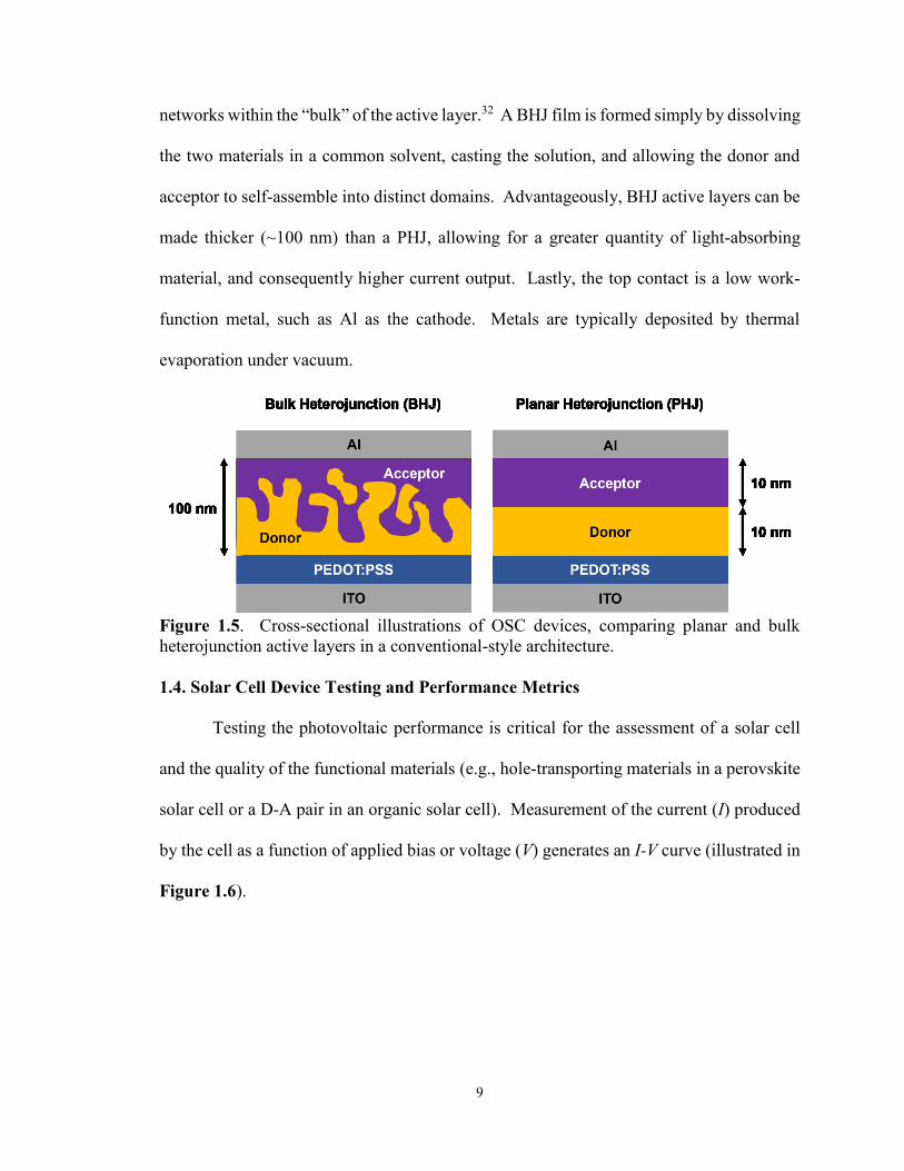
9
networks within the “bulk” of the active layer.32 A BHJ film is formed simply by dissolving
the two materials in a common solvent, casting the solution, and allowing the donor and
acceptor to self-assemble into distinct domains. Advantageously, BHJ active layers can be
made thicker (~100 nm) than a PHJ, allowing for a greater quantity of light-absorbing
material, and consequently higher current output. Lastly, the top contact is a low work-
function metal, such as Al as the cathode. Metals are typically deposited by thermal
evaporation under vacuum.
Figure 1.5. Cross-sectional illustrations of OSC devices, comparing planar and bulk
heterojunction active layers in a conventional-style architecture.
1.4. Solar Cell Device Testing and Performance Metrics
Testing the photovoltaic performance is critical for the assessment of a solar cell
and the quality of the functional materials (e.g., hole-transporting materials in a perovskite
solar cell or a D-A pair in an organic solar cell). Measurement of the current (I) produced
by the cell as a function of applied bias or voltage (V) generates an I-V curve (illustrated in
Figure 1.6).

10
Figure 1.6. An illustration of I-V curves for a SC tested in the dark and in the light (i.e.,
under illumination).
In many cases, current is reported per unit area of the cell as a current density (J).
By convention, the photogenerated current is negative on the I-V curve and the product of
I and V is the power generated by the device (P):
P = IV. (1)
From the I-V (or J-V) curve, many important parameters can be determined. First,
the open-circuit voltage or Voc, occurs when no current flows external to the cell. The
maximum Voc of a perovskite solar cell is the difference in potential energy between the
CBM of the ETL (e.g., TiO2) and the VBM of the HTL; in other words, the Voc is the
difference in potential energy of the excited electron and the collected hole.33 Comparably,
the Voc of an organic solar cell is limited by potential difference between the LUMO of the
acceptor and the HOMO of the donor. The second parameter is the short-circuit current
(Isc or Jsc) which occurs when the voltage equals zero and represents the maximum current

11
output of the SC. Multiplying I by V gives P as a function of V which gives the maximum
power (Pmax) generated by the cell. The current and voltage at the maximum power point
on the I-V curve are Imax and Vmax, respectively. The power conversion efficiency (PCE or
η) is the ratio of Pmax to the power of the incident light (Pin) and is given by the equation:
PCE = Pmax
Pin .
(2)
Another indicator of the overall quality of the cell is the fill-factor (FF), which is
represented graphically by the ratio of the areas depicted on the I-V curve. The fill factor
can be calculated by using Equation (3), which is given by:
FF = Imax ∙ Vmax
Isc ∙ Voc .
(3)
In the absence of light, a solar cell can be modelled as a diode, with current passing in one
direction only (see circuit diagram in Figure 1.7). When illuminated, the cell produces a
photo-generated current (Il). The total output current (I) for an ideal cell is given by
Equation (4) and is the difference of Il and the diode current (ID). Equation (4) is given by:
I = ID − Il = I0 (e(qV/nkT) − 1) − Il .
. (4)
In Equation (4), q is the elementary charge of an electron (1.6×10⁻¹⁹ C), k is the Boltzmann
constant (1.38×10⁻²³ J/K) and T is the operating temperature in Kelvin.

12
Figure 1.7. Circuit diagrams for an ideal solar cell operating under dark and light
conditions and for a real cell, showing sources of parasitic resistances. By convention, the
anode and cathode are defined as the sites of hole and electron collection, respectively. The
“+” and “−” signs indicates the polarity of the applied bias during solar cell operation.
However, in a real solar cell, there are voltage losses due to parasitic series
resistance (RS) and parallel or shunt resistance (RSH). RS is related to the thickness of the
active layer, conductivity of the materials, electrode interfaces and carrier mobilities. RSH
is reflective of the amount of structural and morphological defects in the active layer;
defects decrease RSH, thereby decreasing photovoltaic performance.34 Taking these factors
into account expands the diode current equation to:
I = ID − Il = I0 (e(q(V+I∙RS)/nkT) − 1) − Il +V + I∙RS
RSH .
(5)
13
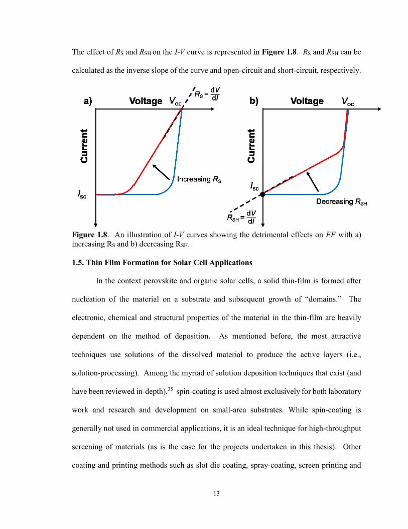
The effect of RS and RSH on the I-V curve is represented in Figure 1.8. RS and RSH can be
calculated as the inverse slope of the curve and open-circuit and short-circuit, respectively.
Figure 1.8. An illustration of I-V curves showing the detrimental effects on FF with a)
increasing RS and b) decreasing RSH.
1.5. Thin Film Formation for Solar Cell Applications
In the context perovskite and organic solar cells, a solid thin-film is formed after
nucleation of the material on a substrate and subsequent growth of “domains.” The
electronic, chemical and structural properties of the material in the thin-film are heavily
dependent on the method of deposition. As mentioned before, the most attractive
techniques use solutions of the dissolved material to produce the active layers (i.e.,
solution-processing). Among the myriad of solution deposition techniques that exist (and
have been reviewed in-depth),35 spin-coating is used almost exclusively for both laboratory
work and research and development on small-area substrates. While spin-coating is
generally not used in commercial applications, it is an ideal technique for high-throughput
screening of materials (as is the case for the projects undertaken in this thesis). Other
coating and printing methods such as slot die coating, spray-coating, screen printing and
14
ink-jet printing are compatible with roll-to-roll (R2R) printing, which can be employed on
large rolls of flexible substrates.
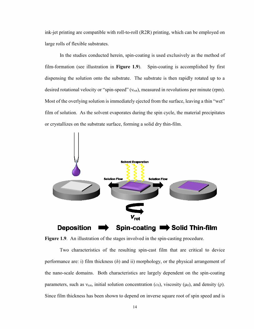
In the studies conducted herein, spin-coating is used exclusively as the method of
film-formation (see illustration in Figure 1.9). Spin-coating is accomplished by first
dispensing the solution onto the substrate. The substrate is then rapidly rotated up to a
desired rotational velocity or “spin-speed” (νrot), measured in revolutions per minute (rpm).
Most of the overlying solution is immediately ejected from the surface, leaving a thin “wet”
film of solution. As the solvent evaporates during the spin cycle, the material precipitates
or crystallizes on the substrate surface, forming a solid dry thin-film.
Figure 1.9. An illustration of the stages involved in the spin-casting procedure.
Two characteristics of the resulting spin-cast film that are critical to device
performance are: i) film thickness (h) and ii) morphology, or the physical arrangement of
the nano-scale domains. Both characteristics are largely dependent on the spin-coating
parameters, such as νrot, initial solution concentration (c0), viscosity (μ0), and density (ρ).
Since film thickness has been shown to depend on inverse square root of spin speed and is
15
directly proportional to c0, 36 h can be controlled relatively easily based on the relationship
given by Equation (6):
h ∝ (μ0
ρ ∙ νrot) 1/2 c0 .
. (6)
However, the morphology is often more difficult to predict than h. Therefore, controlled
experimentation and use of characterization tools to observe the thin-film morphology is
necessary to optimize the spin-coating conditions.
1.6. Project Goals
The overall goal of the research projects herein is to investigate the thin film
properties of the active layers for the production of low-cost and efficient perovskite (e.g.,
CH3NH3PbI3) and organic solar cells. The goal of the first project (Chapter 3) is to
fabricate an efficient perovskite solar cell. The methods involved in the deposition of
perovskite thin films from solution (i.e., the solution-processing conditions) are probed and
correlated to the morphology of perovskite thin films and the performance of the devices.
The second goal of the project (Chapter 4) is reduce the overall cost of the perovskite solar
cell by using cheaper organic hole-transporting materials. The third goal is to assemble a
low-cost non-fullerene donor-acceptor pair for the active layer of an organic solar cell
(Chapter 5). The effect of solution-processing techniques and molecular design on the
thin-film morphology, electronic properties and crystallinity are investigated for
complementary donor-acceptor pairs.

16
CHAPTER 2 – CHARACTERIZATION TECHNIQUES
In order to understand how materials form thin films in perovskite and organic solar
cells, techniques that elucidate the physical and chemical properties of materials in both
bulk form and in thin films are critical.37 This section describes the characterization
techniques and procedures that are applied to perovskite and organic materials and used
throughout this thesis.
2.1. Optical Microscopy (OM)
One of the simplest forms of microscopy is optical microscopy (OM). Since images
acquired by this technique are of low-resolution, it is limited to detecting micrometre-sized
topological film features for rapid screening. However, more powerful techniques are
required to view nano-sized film features. OM images were acquired under transmitted
light using a Zeiss Axio Imager and processed using the Zeiss Zen software package.
2.2. Scanning Electron Microscopy (SEM)
Scanning electron microscopy (SEM) allows the acquisition of higher-resolution
images than OM. A focused beam of electrons is raster scanned across the sample surface.
Secondary electrons are ejected from the sample and detected to generate a 2D image of
the film surface. In this thesis, SEM was used exclusively to image the surfaces of
perovskite films as a tool to detect pinholes and assess film coverage. All surface SEM
images were acquired using a Phenom G2 Pro bench-top SEM with backscatter detection,
in the laboratory of Prof. Jeffery Dahn.
2.3. Atomic Force Microscopy (AFM)
Atomic force microscopy (AFM) is advantageous over the aforementioned forms
of microscopy for the ability to elucidate the three-dimensional (3D) topography of the film
surface for quantification of domain sizes and height deviations. For this reason, AFM is
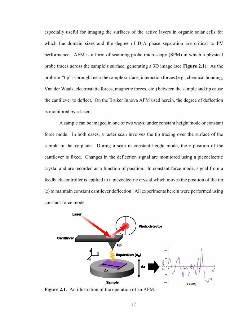
17
especially useful for imaging the surfaces of the active layers in organic solar cells for
which the domain sizes and the degree of D-A phase separation are critical to PV
performance. AFM is a form of scanning probe microscopy (SPM) in which a physical
probe traces across the sample’s surface, generating a 3D image (see Figure 2.1). As the
probe or “tip” is brought near the sample surface, interaction forces (e.g., chemical bonding,
Van der Waals, electrostatic forces, magnetic forces, etc.) between the sample and tip cause
the cantilever to deflect. On the Bruker Innova AFM used herein, the degree of deflection
is monitored by a laser.
A sample can be imaged in one of two ways: under constant height mode or constant
force mode. In both cases, a raster scan involves the tip tracing over the surface of the
sample in the xy plane. During a scan in constant height mode, the z position of the
cantilever is fixed. Changes in the deflection signal are monitored using a piezoelectric
crystal and are recorded as a function of position. In constant force mode, signal from a
feedback controller is applied to a piezoelectric crystal which moves the position of the tip
(z) to maintain constant cantilever deflection. All experiments herein were performed using
constant force mode.
Figure 2.1. An illustration of the operation of an AFM.
18
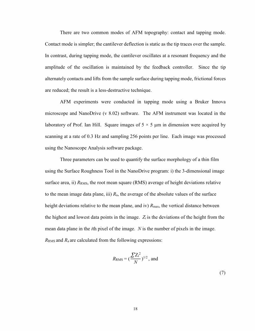
There are two common modes of AFM topography: contact and tapping mode.
Contact mode is simpler; the cantilever deflection is static as the tip traces over the sample.
In contrast, during tapping mode, the cantilever oscillates at a resonant frequency and the
amplitude of the oscillation is maintained by the feedback controller. Since the tip
alternately contacts and lifts from the sample surface during tapping mode, frictional forces
are reduced; the result is a less-destructive technique.
AFM experiments were conducted in tapping mode using a Bruker Innova
microscope and NanoDrive (v 8.02) software. The AFM instrument was located in the
laboratory of Prof. Ian Hill. Square images of 5 × 5 µm in dimension were acquired by
scanning at a rate of 0.3 Hz and sampling 256 points per line. Each image was processed
using the Nanoscope Analysis software package.
Three parameters can be used to quantify the surface morphology of a thin film
using the Surface Roughness Tool in the NanoDrive program: i) the 3-dimensional image
surface area, ii) RRMS, the root mean square (RMS) average of height deviations relative
to the mean image data plane, iii) Ra, the average of the absolute values of the surface
height deviations relative to the mean plane, and iv) Rmax, the vertical distance between
the highest and lowest data points in the image. Zi is the deviations of the height from the
mean data plane in the ith pixel of the image. N is the number of pixels in the image.
RRMS and Ra are calculated from the following expressions:
RRMS = (∑ Zi
2
N)1/2 , and
(7)
19
𝑅a = 1
N ∑ |Zi|
N
i = 1
.
(8)
2.4. X-ray Diffraction (XRD)
XRD experiments are used to: i) identify the materials present and ii) assess the
crystallinity of materials within the thin films. Insight into the arrangement of molecules
within the crystallites in the films can be gained using Bragg’s Law:
nλ = 2dsinθ (9)
where n is an integer, λ is the wavelength of incident radiation from the instrument, θ is the
angle of incidence of X-rays with respect to the atomic planes of the crystal and d is the
separation distance of the atomic planes (i.e., spacing). The Rigaku diffractometer used for
the XRD experiments has a Cu-Kα radiation source, so the X-rays produced have a
wavelength of 1.54 Å.38
XRD patterns were acquired using a Rigaku Ultima IV X-ray diffractometer
equipped with a CuKα radiation source, scintillation detector, fixed monochromator and
285 nm focusing slit. The film-coated substrates were mounted into the instrument on a
metal platform. Experiments were run using the RINT2200 Right software package with
divergence and receiving slit widths of 10 mm and 0.3 mm, respectively, and an offset
angle of 0°. Powder patterns were acquired by continuous scans, collecting data as counts
per second (cps) and scanning at a rate of 2° per minute. The patterns in each data set were
normalized such that the level of the noise is equivalent, that is, the intensity of the pattern
at a Bragg angle of 3.05°.
2.5. UV-Visible (UV-Vis) Spectroscopy

20
UV-Visible spectroscopy (UV-Vis) can be performed on conjugated organic
molecules in solid-state thin films or dissolved in solution. The absorption profile provides
information about the energy of the light absorbed by the material, which is related to the
bandgap energy (Eg), or the difference between the HOMO and LUMO energy levels. Eg
is determined from the wavelength of the onset of absorption (λonset), or the longest
wavelength of visible light that is absorbed by the material, and applying Equation (10):
Eg =h∙c
λonset .
(10)
In Equation (10), h is the Planck constant (4.136×10⁻¹⁵ eV∙s) and c is the speed of light
in vacuum (2.998×10⁸ m/s). All UV-Vis spectra were acquired using an Agilent Cary 60
spectrophotometer with the Cary Scan software program. For thin-film experiments, the
film-coated glass substrates were mounted vertically into the instrument with the glass side
facing the radiation source. The instrument was first zeroed using a clean glass slide as a
blank. Spectra were acquired by scanning from 900 nm to 200 nm at a rate of 600 nm/min.
The spectra were normalized to the peak absorbance value. All solution samples were
prepared by stirring a weighed quantity of each material in a vial with CHCl3 or
chlorobenzene (CB) as the solvent until dissolved. After transferring the solutions into
quartz cuvettes, UV-Vis spectra were acquired by scanning from 900 nm to 200 nm at a
rate of 600 nm/min.
2.6. Photoluminescence (PL) Spectroscopy
The term photoluminescence (PL) refers to the emission of photons following
photoexcitation. Photoexcitation occurs when electrons are promoted to higher-energy
states upon absorption of light. As the electrons relax to the ground-state via various
21
mechanisms, photons can be re-radiated and detected by the PL instrument. During PL
experiments, the sample is irradiated by visible light of a particular wavelength (excitation
wavelength, λex) and an emission spectrum is recorded.
The film-coated substrates were mounted vertically into the instrument with the
film-side facing the radiation source at a 45° angle. For emission experiments, λex was
selected as the wavelength at which maximum absorption for the particular material occurs
in a thin film (determined from the results of thin-film UV-Vis experiments). Excitation
and emission slit widths were set to 20 nm. Spectra were acquired by scanning at a rate of
600 nm/min.
2.7. Cyclic Voltammetry (CV)
CV was used to measure the onset of oxidation and reduction of the materials, which
corresponds to the ionization potential (HOMO) and electron affinity (LUMO),
respectively. This information is critical in D-A organic solar cells, where the efficient
charge separation at the D-A interface depends on appropriate alignment of the HOMO and
LUMO energy levels.
CV experiments for organic materials were conducted using solution samples. A
BASi CV instrument was equipped with an N2 bubbler as well as an Ag/AgCl electrode, Pt
wire and glassy-carbon electrode as the pseudo-reference, counter electrode and working
electrode, respectively. Measurements were conducted using the BASi Epsilon EC
software program. Samples were prepared with a concentration of ~1 mg/mL by dissolving
each material in anhydrous CH2Cl2 with ~0.1 M tetrabutylammoniumhexafluorophosphate
(TBAPF6) as the supporting electrolyte. All solutions were purged with N2(g) and then
scanned at 50, 100 and 150 mV/s as-is and at 100 mV/s after the addition of a ferrocene

22
(Fc) standard. The resulting voltammograms were referenced to the oxidation potential of
Fc/Fc+, which corresponds to the HOMO energy level at a value of 4.80 eV below the
vacuum level.39 The values of the HOMO and LUMO energy levels of the organic
compounds were obtained by comparing the onset of oxidation and reduction, respectively,
to the HOMO energy of ferrocene.
23
CHAPTER 3 – THIN FILM FORMATION IN PEROVSKITE SOLAR CELLS
3.1. Background
3.1.1. Solution-Processed Perovskite Solar Cells
The combination of interesting material properties and the reported high
performance of perovskite solar cellss make perovskites an attractive field of study. For
this reason, it was a collective decision to develop a research program in the Welch and
Hill laboratories focused on the development and characterization of materials for PSCs.
Before the study of novel materials could be conducted, it was necessary to develop
an in-house fabrication procedure for reproducible and high-efficiency standard devices to
serve as controls. While many reports in the literature exist, fabricating a PSC is not a
straight-forward process and ultimately depends on film formation of the active layer. This
chapter serves as an account of the challenges encountered during the development of a
functional perovskite solar cell.
3.1.2. Active Layer Components and Device Architecture
There are two general types of active layers for PSCs: Meso-structured and planar
heterojunction (PHJ) (see Figure 3.1). In mesostructured PSCs the perovskite material is
housed within a mesoporous scaffolding of semiconducting (e.g., TiO2)17 or insulating
(Al2O3)40,41 nanoparticles. In contrast, a planar heterojunction perovskite solar cell does
not contain the mesoporous oxide layer; the active layer is simply an unsupported thin film
of perovskite material.42,43 While preliminary mesoporous devices were fabricated (results
are not reported in this thesis), the PHJ architecture was selected for further optimization
due to its simplicity in construction.

24
Figure 3.1. Device architectures for planar and meso-structured perovskite solar cells.
For planar perovskite solar cells, a mixed halide perovskite (CH3NH3PbI3-xClx) is a
preferred material for planar architectures because of the longer electron-hole diffusion
length44 than its pure-halide45 counterpart (CH3NH3PbI3). Nevertheless, pure-halide (i.e.,
MAPbI3) perovskites have been used in planar cells with high efficiencies.24,46 For this
reason, MAPbI3 is the perovskite material used in the studies throughout this thesis.
Regardless of the material selection, film uniformity of the perovskite active layer
is critical for high performance devices and is difficult to achieve. It has been demonstrated
that controlled vapour deposition is an effective method that can achieve uniform films and
highly efficient planar cells with both mixed- and pure-halide perovskite active layers.24,47
However, this method is expensive and challenging on an industrial scale. On the other
hand, solution-processing is a cost-effective method for active layer deposition and is
necessary to realize large-scale R2R production of perovskite solar cells.48
3.1.3. Methods of Solution-Processed Perovskite Thin Films
One of the most important factors that influences the performance of a planar
heterojunction perovskite solar cell is the active layer film morphology (e.g., crystal grain

25
size, crystal distribution, overall uniformity and coverage, absence of pinholes, etc.).
Furthermore, the film morphology is largely dependent on the processing methods and
conditions applied during film formation.
Three well-documented methods exist for perovskite film formation from solution:
i) Co-Deposition. The perovskite is formed in-situ by spin-coating a single
solution containing the two constituents (i.e., methyl ammonium iodide
(CH3NH3I or “MAI”) and lead (II) iodide (PbI2)).17,49
ii) Sequential Dip-Coating (SDC). A film of the metal halide is first deposited on
the substrate via spin-coating and then dipped into a solution containing the
ammonium salt. In this method, (which was first documented by Liang et al),50
PbI2 and MAI react to form the final perovskite film. This method has proven
to be an effective active-layer processing technique in perovskite solar cells,
helping to fabricate devices that achieve over 15% efficiency.46,51 In addition,
modifications to the two-step method to control PbI2 crystal growth via solvent
engineering have been discovered that yield devices with over 16%.52
iii) Sequential Spin-Coating (SSC). Similar to the SDC method, a thin film of PbI2
is first deposited onto the substrate.53 Subsequently, a film of MAI is spin-
coated on top of the PbI2 layer. Heating the layers stimulates the interdiffusion
of MAI ions into the underlying PbI2 film, forming the perovskite, MAPbI3.
The first goal in this project was to screen previously-reported methods for perovskite
film formation. However, processing conditions vary from lab to lab – the optimal
conditions for film formation reported in the literature are not universal. Furthermore, it
was found that many subtle techniques and “tricks-of-the-trade” are often excluded from
experimental sections of “high-impact” papers. For these reasons, it was important to
26
identify variables and perform controlled sets of optimization experiments to develop a
custom in-house method for perovskite film formation. Methods for both SDC and SSC
were developed and discussed herein.
3.2. Sequential Dip-Coating Experimental Methods
3.2.1. PbI2 and MAPbI3 Thin Films
Thin films of PbI2 and MAPbI3 were prepared via spin-coating on TiO2-coated glass
substrates to determine the optimal processing conditions. The procedure for making these
films was as follows.
25 mm × 25 mm glass slides were first cleaned in the following order: i) scrubbing
with mixture of deionized (DI) H2O and Sparkleen® detergent, ii) rinsing with DI H2O, iii)
rinsing with acetone, iv) rinsing with isopropanol, v) drying under a stream of air and iv)
UV/ozone treatment for 15 min.
The clean substrate was first mounted onto the chuck of a Laurell spin-coater. To
form the dense TiO2 layer, the precursor solution (see Appendix A for preparation
procedure) was dispensed onto the center of the 625-mm2 substrate through a 0.45 μm
PVDF filter using a 1 mL syringe in one aliquot of 0.3 mL. The film was then spun at 2000
rpm (ramp = 2050 rpm/s) for 45 seconds. The coated substrates were placed in clean
Pyrex® petri dishes and then placed in a sintering oven. The temperature was ramped up
to 500 °C at a rate of 30 °C/min and held at 500 °C for 30 min. The films were then
removed from the oven and cooled to room temperature (RT).
To form the PbI2 films, PbI2 solutions with N,N-dimethylformamide (DMF) as the
solvent were prepared (see Appendix A for preparation procedure). At a concentration of
1.0 M, the solution was supersaturated at RT and had to be cast at an elevated temperature.
The dilute solutions (i.e., 0.5 M and 0.75 M) were cast at RT.

27
The TiO2-coated glass substrates were used either heated (on a hotplate) or unheated
(at RT). After placing the substrate onto the chuck of the spin-coater, approximately 0.3
mL of solution was retracted from the vial using a 1.0 mL syringe and dispensed onto the
center of the substrate through a 0.45 µm PTFE filter in a single aliquot. The spin-coater
was then run at speeds of either 1000, 3000 and 5000 rpm for 30 s. For heated substrates,
the average elapsed time from removal of the substrate from the heat source and solution
deposition was 30 s.
The dipping solutions were prepared by weighing the dried MAI (dried in a vacuum
oven overnight prior to solution preparation) into a 30 mL beaker, adding the appropriate
amount of isopropanol to form a 10 mg/mL solution and then stirring the solution at RT
(using a stir bar and a hotplate) for approximately 15 min. The synthesis of MAI is
described in Appendix B. To initiate the conversion into a MAPbI3 perovskite film, the
PbI2 films were briefly rinsed a beaker containing isopropanol, removed, and then
immersed in the beaker containing the MAI solution. The beaker was gently swirled by
hand for 60 s to promote uniform diffusion of the MAI across the entire PbI2 film surface.
After 60 s, the substrate was removed from the dipping solution using tweezers, rinsed in a
beaker of isopropanol and finally dried under a stream of filtered air or N2. The perovskite
films were characterized as-is without further processing and stored in an Ar-filled
glovebox. The SDC procedure is illustrated in Figure 3.2.
28
Figure 3.2. Photographs depicting the stages of the SDC procedure.
3.2.2. Perovskite Solar Cell Fabrication Using Sequential Dip Coating
The 25 mm × 25 mm FTO-glass substrates were first cleaned by the following
procedure: i) scrubbing the surface with lab detergent (Sparkleen®) and DI H2O, ii)
sonicating in a solution of DI H2O and Sparkleen® for 15 min, iii) sonicating in acetone
for 15 min, iv) sonicating in ethanol for 15 min, iv) rinsing in DI H2O and v) UV/ozone
treatment for 20 min.
The TiO2 film was deposited immediately following UV/ozone treatment using the
method described in Section 3.2.1. Before entering the oven, the four corners of the
substrate were carefully wiped with a CleanSwab® dampened with 37% HCl to expose the
underlying FTO. The substrates were then placed in a Pyrex® petri dish and then baked in
the sintering oven at 500 °C for 30 min. After cooling to room-temperature, the substrates
were either heated on a hotplate to establish the desired Tsubstrate or used unheated.
Only 1.0 M PbI2 solutions were used to make PbI2 films for PSCs. For deposition
on heated substrates, the substrates were removed from the hotplate and quickly placed
onto the chuck of the spin-coater. Approximately 0.3 mL of the hot PbI2 solution was
retracted into a 1.0 mL syringe and then quickly dispensed onto the center of the heated
substrate through a 0.45 µm PTFE filter in one aliquot. The spin-coater was then run at

29
speeds of either 1000 or 3000 rpm for 30 s. The four corners were then wiped with
CleanSwab® dampened with DMF to expose the underlying FTO. The PbI2 films were
converted into MAPbI3 in all devices following the procedure outlined in Section 3.2.1.
To form the hole-transporting layer, the solution containing p-doped spiro-
OMeTAD (see Appendix A for preparation procedure) was dispensed onto the perovskite
layer through a 0.45 µm PTFE filter and then spun at a rate of 4000 rpm for 30 s under
ambient conditions. The four corners were then wiped with a CleanSwab® dampened with
chlorobenzene to expose the underlying FTO.
The top metal contact was deposited via thermal evaporation. The substrates were
loaded top-down into a metal mask and then mounted in a custom-built bell-jar thermal
evaporator. A silver slug was used as the metal source in a tungsten-wire basket. The bell-
jar was evacuated using a diffusion pump to a pressure less than 4×10⁻⁶ Torr. A 75-nm
thick layer of silver was deposited onto the substrates by thermal evaporation. After
removal from the bell-jar, the devices were immediately transferred into an Ar-filled
glovebox where they were tested and subsequently stored.
3.3. Perovskite Solar Cell Device Characterization
For photovoltaic measurements, solar cell devices were illuminated using a
calibrated light source. A National Institute of Standards and Technology (NIST)-traceable
calibrated photodiode (Newport 818-UV-L) in conjunction with a near infrared absorptive
filter (Thorlabs NENIR60A) was used to measure the output power density of the Xe arc
lamp (Sciencetech SS0.5K) below 800 nm, where the spectrum of the source closely
matches the solar spectrum and covers the absorption range of all photoactive materials
used in this thesis. This provided a power density of 100 (±1) mW/cm2 of AM 1.5G
spectrum over relevant wavelengths, or the equivalent of 1.00 Suns. Each device had an
30
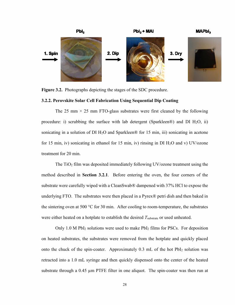
area of 0.032 cm2 and was tested in separate measurements. One exposed FTO corner was
contacted with the negative (black) electrode and the Ag top contact of a device was
contacted by gently approaching a thin gold-wire that was connected to the positive (red)
electrode (illustrated in Figure 3.3). Current-voltage (I-V) curves were then measured
using a Keithley source-measure unit, scanning from +2.0 V to short-circuit (0.0 V) unless
otherwise stated.
Figure 3.3. A photograph of a substrate with 16 completed PSC devices. The points of
contact to the positive and negative electrode are indicated by red and black arrows,
respectively.
3.4. Results and Discussion – Sequential Dip-Coating
While investigating the sequential dip-coating (SDC) method for perovskite thin
film formation, it was found that the morphology of the final perovskite film is largely
dependent on the morphology of the initial PbI2 film. A major issue was the formation of
large, needle-like crystals of PbI2, which formed cloudy, non-continuous films with poor
substrate-coverage, unsuitable for the active layer of PSCs. Perovskite active layers with
maximum surface coverage are desired in devices to prevent shunt pathways and short-

31
circuits. Therefore, methods that generate dense perovskite layers with a uniform
distribution of crystallites are favoured.
Rapid cooling of the hot solution during spin-coating of the PbI2 was identified as
a cause for the large-crystal growth. Various spin-coating parameters were systematically
controlled to investigate the effect on film morphology. The solution concentration
(Csolution), spin speed (νrot), and substrate temperature (Tsubstrate) were found to have the most
significant effect on film morphology. Conditions including the solution temperature
(Tsolution, Figure C1) and atmosphere (Figure C2) were also investigated and are discussed
in Appendix C.
3.4.1. Solution Concentration (Csolution) and Spin Speed
The most common solution used in the literature for the deposition of the PbI2 film
during the two-step perovskite deposition method is a 1.0 M (461 mg/mL) solution in DMF.
While this solution has proven to yield thick, uniform films in devices with high
efficiencies, its use is problematic: it is a supersaturated solution at room temperature and
must be deposited at elevated temperatures (i.e., “hot-cast”). Following this procedure,
there is a tendency for the PbI2 to rapidly crystallize on the substrate before the film is spun.
By reducing the concentration, it is possible to deposit a homogeneous solution of PbI2
without the need for hot-casting. Figure 3.4 depicts OM images of PbI2 films deposited
from solutions of different concentrations and different spin speeds onto substrates held at
room temperature. It was observed that film uniformity and coverage increases with
increasing spin velocity – a phenomenon that was also observed by Cohen et al.54 The
crystalline domain sizes decrease with increasing spin velocity. This is attributed to the
higher rate of solvent evaporation as the spin speed is increased. From the optical
microscope images, it is clear that perovskite films cast from 1.0 M solutions provide better

32
substrate coverage and are more desirable as active layers in PSC devices than those cast
from more dilute solutions (Figure 3.5). For this reason, all further modifications to
processing conditions in this study were performed using 1.0 M solutions.
Figure 3.4. Optical microscope images of PbI2 films spin-cast on TiO2 compact films
showing the effect of precursor-solution concentration. The 0.5 and 0.75 M solutions were
deposited at room temperature and spun for 90 s. The 1.0 M solution was deposited at 70
°C and spun for 30 s. All films were cast onto room-temperature substrates.
Figure 3.5. SEM images of the CH3NH3PbI3 films after conversion of the PbI2 films via
SDC, showing the effect of precursor-solution concentration.
33
3.4.2. Substrate Temperature (Tsubstrate)
To reduce the rate of cooling of the solution after dispensing it onto the cold
substrate, films were cast onto heated substrates (from 50 °C up to 150 °C) and compared
to those cast onto unheated substrates (Figure 3.6). It is important to note that the substrate
cools considerably between the time of heating and the time when the solution is dispensed.
To determine the substrate temperatures (Tsubstrate), a thermocouple probe was attached to
the surface of the substrate using Kapton® tape. The initial substrate temperature
(Tsubstrate,initial) was recorded while the substrate was resting on the hotplate with a surface
temperature of Thotplate. These measurements were recorded after at least 10 minutes of
heating. The final substrate temperature (Tsubstrate,final) was recorded 30 s after the substrate
was removed from the heat source and placed on the chuck of the spin-coater. The
measurements for substrate temperatures are listed in Table 3.1.
It was observed that glass microscope slides, which are considerably thinner than
the FTO-coated glass substrates used for device fabrication, have a higher rate of cooling.
For instance, if a glass microscope slide and an FTO-coated glass substrate are heated to
100 °C and 75 °C, respectively, both will cool to a temperature of 60 °C after being placed
on the chuck of the spin-coater for 30 s (i.e., Tsubstrate,final is ~ 60 °C).
Table 3.1. Initial and final (i.e., after 30 s) temperatures of glass and FTO substrates heated
on a hotplate set to a surface temperature of Thotplate.
Tsubstrate,initial
(°C)
Thotplate
(°C)
Tsubstrate,final
(°C) (Glass)
Tsubstrate,final
(°C) (FTO)
50 66 40 46
75 92 49 59
100 117 60 69
125 135 65 85
150 160 73 105
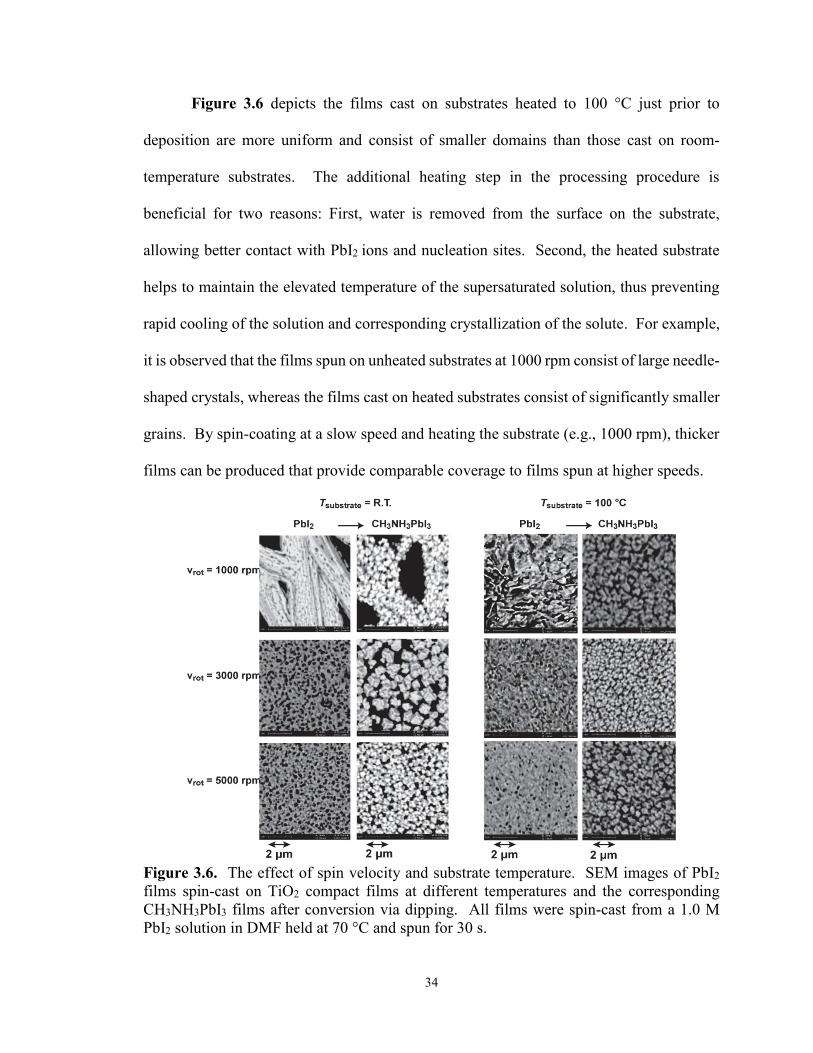
34
Figure 3.6 depicts the films cast on substrates heated to 100 °C just prior to
deposition are more uniform and consist of smaller domains than those cast on room-
temperature substrates. The additional heating step in the processing procedure is
beneficial for two reasons: First, water is removed from the surface on the substrate,
allowing better contact with PbI2 ions and nucleation sites. Second, the heated substrate
helps to maintain the elevated temperature of the supersaturated solution, thus preventing
rapid cooling of the solution and corresponding crystallization of the solute. For example,
it is observed that the films spun on unheated substrates at 1000 rpm consist of large needle-
shaped crystals, whereas the films cast on heated substrates consist of significantly smaller
grains. By spin-coating at a slow speed and heating the substrate (e.g., 1000 rpm), thicker
films can be produced that provide comparable coverage to films spun at higher speeds.
Figure 3.6. The effect of spin velocity and substrate temperature. SEM images of PbI2
films spin-cast on TiO2 compact films at different temperatures and the corresponding
CH3NH3PbI3 films after conversion via dipping. All films were spin-cast from a 1.0 M
PbI2 solution in DMF held at 70 °C and spun for 30 s.
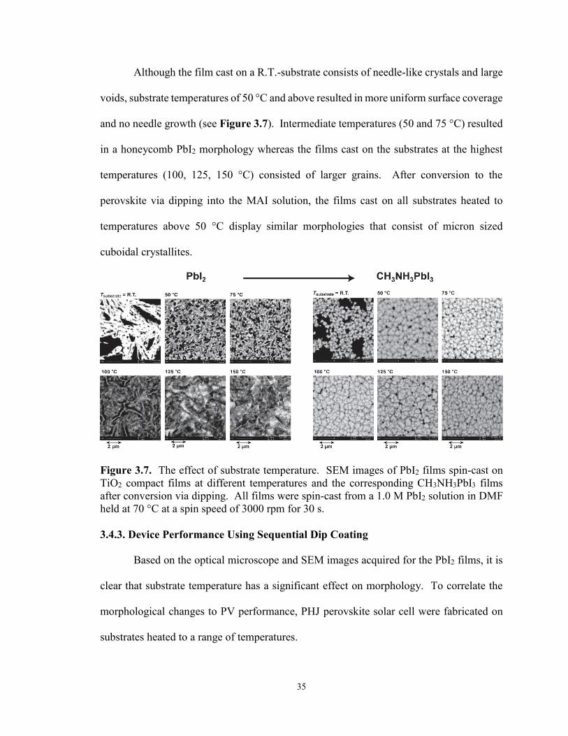
35
Although the film cast on a R.T.-substrate consists of needle-like crystals and large
voids, substrate temperatures of 50 °C and above resulted in more uniform surface coverage
and no needle growth (see Figure 3.7). Intermediate temperatures (50 and 75 °C) resulted
in a honeycomb PbI2 morphology whereas the films cast on the substrates at the highest
temperatures (100, 125, 150 °C) consisted of larger grains. After conversion to the
perovskite via dipping into the MAI solution, the films cast on all substrates heated to
temperatures above 50 °C display similar morphologies that consist of micron sized
cuboidal crystallites.
Figure 3.7. The effect of substrate temperature. SEM images of PbI2 films spin-cast on
TiO2 compact films at different temperatures and the corresponding CH3NH3PbI3 films
after conversion via dipping. All films were spin-cast from a 1.0 M PbI2 solution in DMF
held at 70 °C at a spin speed of 3000 rpm for 30 s.
3.4.3. Device Performance Using Sequential Dip Coating
Based on the optical microscope and SEM images acquired for the PbI2 films, it is
clear that substrate temperature has a significant effect on morphology. To correlate the
morphological changes to PV performance, PHJ perovskite solar cell were fabricated on
substrates heated to a range of temperatures.

36
When keeping the spin speed constant at 3000 rpm, increasing the temperature of
the substrate decreases cell performance in terms of efficiency and current density (Figure
3.8 and Table 3.2). However, the devices with PbI2 films cast at 1000 rpm benefit from
substrate heating (Figure 3.9 and Table 3.3). By heating the substrate to 100 °C prior to
deposition, the resulting devices display a higher shunt resistance. This is in agreement
with the optical microscope images of the PbI2 and perovskite films; films cast on the heated
substrates show visibly greater coverage and correspondingly higher RSH.
Figure 3.8. a) J-V curves for the best-performing PSCs with PbI2 films deposited at 3000
rpm on substrates heated and unheated substrates. b) A plot of the average PCE of PSC
devices with PbI2 films deposited at 3000 rpm as a function of substrate temperature. For
each substrate temperature, error bar range extends from the lowest- to the highest-observed
PCE among five representative devices.
Table 3.2. J-V performance metrics for the best-performing PSCs fabricated with PbI2
films deposited at 3000 rpm on substrates heated and unheated substrates. The average
metrics for five sample devices (at each substrate temperature) are also provided with
standard deviations in the brackets.
νrot (rpm) Tsubstrate
(°C) Voc (V) Jsc (mA cm-2) PCE (%) FF
3000 R.T. Best Cell 0.97 −18.20 9.76 0.56
Average 0.93(0.02) −18.12(0.26) 7.48(2.01) 0.44(0.11)
3000 100 Best Cell 0.93 −14.52 5.31 0.39
Average 0.92(0.01) −14.43(0.56) 4.99(0.42) 0.38(0.02)
3000 150 Best Cell 0.62 −8.67 1.91 0.36
Average 0.56(0.07) −8.79(1.01) 1.76(0.14) 0.36(0.00)
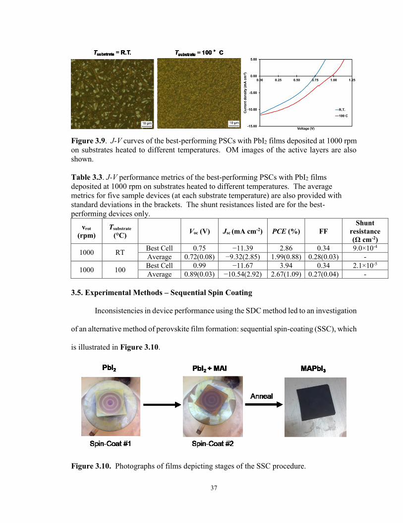
37
Figure 3.9. J-V curves of the best-performing PSCs with PbI2 films deposited at 1000 rpm
on substrates heated to different temperatures. OM images of the active layers are also
shown.
Table 3.3. J-V performance metrics of the best-performing PSCs with PbI2 films
deposited at 1000 rpm on substrates heated to different temperatures. The average
metrics for five sample devices (at each substrate temperature) are also provided with
standard deviations in the brackets. The shunt resistances listed are for the best-
performing devices only.
νrot
(rpm)
Tsubstrate
(°C) Voc (V) Jsc (mA cm-2) PCE (%) FF
Shunt
resistance
(Ω cm-2)
1000 RT Best Cell 0.75 −11.39 2.86 0.34 9.0×10⁻⁴
Average 0.72(0.08) −9.32(2.85) 1.99(0.88) 0.28(0.03) -
1000 100 Best Cell 0.99 −11.67 3.94 0.34 2.1×10⁻⁵
Average 0.89(0.03) −10.54(2.92) 2.67(1.09) 0.27(0.04) -
3.5. Experimental Methods – Sequential Spin Coating
Inconsistencies in device performance using the SDC method led to an investigation
of an alternative method of perovskite film formation: sequential spin-coating (SSC), which
is illustrated in Figure 3.10.
Figure 3.10. Photographs of films depicting stages of the SSC procedure.
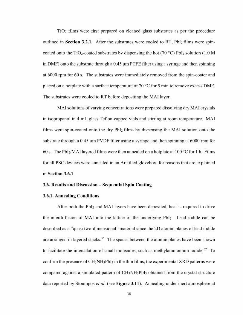
38
TiO2 films were first prepared on cleaned glass substrates as per the procedure
outlined in Section 3.2.1. After the substrates were cooled to RT, PbI2 films were spin-
coated onto the TiO2-coated substrates by dispensing the hot (70 °C) PbI2 solution (1.0 M
in DMF) onto the substrate through a 0.45 μm PTFE filter using a syringe and then spinning
at 6000 rpm for 60 s. The substrates were immediately removed from the spin-coater and
placed on a hotplate with a surface temperature of 70 °C for 5 min to remove excess DMF.
The substrates were cooled to RT before depositing the MAI layer.
MAI solutions of varying concentrations were prepared dissolving dry MAI crystals
in isopropanol in 4 mL glass Teflon-capped vials and stirring at room temperature. MAI
films were spin-coated onto the dry PbI2 films by dispensing the MAI solution onto the
substrate through a 0.45 μm PVDF filter using a syringe and then spinning at 6000 rpm for
60 s. The PbI2/MAI layered films were then annealed on a hotplate at 100 °C for 1 h. Films
for all PSC devices were annealed in an Ar-filled glovebox, for reasons that are explained
in Section 3.6.1.
3.6. Results and Discussion – Sequential Spin Coating
3.6.1. Annealing Conditions
After both the PbI2 and MAI layers have been deposited, heat is required to drive
the interdiffusion of MAI into the lattice of the underlying PbI2. Lead iodide can be
described as a “quasi two-dimensional” material since the 2D atomic planes of lead iodide
are arranged in layered stacks.55 The spaces between the atomic planes have been shown
to facilitate the intercalation of small molecules, such as methylammonium iodide.52 To
confirm the presence of CH3NH3PbI3 in the thin films, the experimental XRD patterns were
compared against a simulated pattern of CH3NH3PbI3 obtained from the crystal structure
data reported by Stoumpos et al. (see Figure 3.11). Annealing under inert atmosphere at

39
100 °C for 1 hour results in full conversion to the perovskite, as indicated by absence of the
110 PbI2 peak (2θ = 12.6°) in the thin-film XRD patterns Figure 3.11. On the other hand,
the films that were annealed in ambient conditions for 1 hour contained unconverted PbI2.
It is possible that the moisture in air contributes to degradation of the perovskite into lead
iodide, which has been demonstrated in a previous study by Kelly et al.56 No significant
differences were observed in terms of morphology for the films annealed in ambient versus
those annealed in inert atmosphere (see Figure 3.12). Based on these results, all subsequent
perovskite films were annealed in an Ar-filled glovebox.
Figure 3.11. XRD pattern of a PbI2 thin film on TiO2 compared to CH3NH3PbI3 films after
annealing at 100 °C for 1 h in inert (black trace) or ambient (grey trace) atmosphere. The
simulated powder pattern (blue trace) was obtained from the CH3NH3PbI3 crystal structure
data (in the form of a cif file) reported by Stoumpos et al.18 The corresponding lattice
planes for each of the diffraction peaks in the PbI2 pattern ((001), (002) and (003)) were
identified according to Burschka et al.51 The peaks corresponding to the major lattice
planes in the CH3NH3PbI3 patterns ((110), (220) and (330)) were identified based on the
analysis performed by Dualeh et al.57

40
Figure 3.12. 2D AFM topographical maps of the surface of two perovskite films formed
by the sequential spin-coating method – one was annealed in ambient and one annealed in
an inert atmosphere.
3.6.2. MAI Concentrations
In order to establish the correct stoichiometry between the PbI2 and MAI layers for
complete perovskite conversion, a series CH3NH3PbI3 films were formed by sequential spin
coating using different concentrations of MAI solution. For all films, the PbI2 spin speed
(6000 rpm), PbI2 solution concentration (1.0 M), MAI spin speed (6000 rpm), PbI2-MAI
annealing time (60 min) and annealing temperature (100 °C) were kept constant.
XRD was used to detect the phases of the materials present in the final films (Figure
3.13). The intensity of the (110) PbI2 peak (2θ = 12.6°) decreased linearly with increasing
MAI concentrations, indicating that less PbI2 remains unreacted in the film (Figure 3.14).
Visually, the films with a higher MAI loading appear darker and more optically dense due
to the higher quantities of MAPbI3 (see photographs of films in Figure 3.13). As shown
in the XRD patterns in Figure 3.13, perovskite thin films spin-coated with MAI solutions
less than 50 mg/mL all contained (001), (002) and (003) PbI2 diffraction peaks of
significant intensity. A plot of the relative intensity of the (001) PbI2 peak in the perovskite
powder patterns as a function of MAI concentration is provided in Figure 3.14 and shows

41
a linear decrease in peak intensity with increasing MAI concentration. This provides
evidence for presence of unreacted starting material and incomplete perovskite conversion
when using dilute MAI concentrations.
Figure 3.13. XRD patterns of MAPbI3 thin film formed via the sequential spin-coating
method with different concentrations of MAI precursor solution. All films were annealed
at 100 °C under inert atmosphere after spin-coating the MAI and PbI2 layers. A powder
patterns of a PbI2 neat film is included at the bottom of the plot for comparison. Also shown
are photographs of the MAPbI3 films, showing progressive darkening of the film with
increasing MAI concentration.

42
Figure 3.14. Relative XRD peak intensities for the highest-intensity peak of a) PbI2 and b)
MAI plotted as a function of MAI precursor concentration. The relative peak intensity was
determined by dividing the integrated intensity of the (001) PbI2 peak (IPbI2) by the sum of
IPbI2 and the intensities of the MAPbI3 (110) peak (2θ = 14.1°). Areal peak intensities were
calculated by applying a Pearson VII function using Jade software. Although error bars
are included in the plot, they are not visible. Measures of uncertainty associated with the
calculated peak intensities are listed in Table D1 in Appendix D.
3.6.3. Device Performance Using Sequential Spin-Coating
Perovskite solar cell devices were fabricated to determine the optimal MAI
precursor solution concentration for the sequential spin-coating method. All other
components in the devices were fabricated following the same procedures used for the
devices made via the dip method. Devices made with the higher loading of MAI (50
mg/mL) were more efficient as indicated by the J-V curves in Figure 3.15. These results
are comparable to devices made using similar procedures, in which the reported PCEs of
sample devices are 13.4 %58,59 and 15.4 %.53 Comparing the J-V results to the XRD
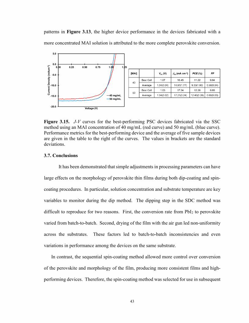
43
patterns in Figure 3.13, the higher device performance in the devices fabricated with a
more concentrated MAI solution is attributed to the more complete perovskite conversion.
Figure 3.15. J-V curves for the best-performing PSC devices fabricated via the SSC
method using an MAI concentration of 40 mg/mL (red curve) and 50 mg/mL (blue curve).
Performance metrics for the best-performing device and the average of five sample devices
are given in the table to the right of the curves. The values in brackets are the standard
deviations.
3.7. Conclusions
It has been demonstrated that simple adjustments in processing parameters can have
large effects on the morphology of perovskite thin films during both dip-coating and spin-
coating procedures. In particular, solution concentration and substrate temperature are key
variables to monitor during the dip method. The dipping step in the SDC method was
difficult to reproduce for two reasons. First, the conversion rate from PbI2 to perovskite
varied from batch-to-batch. Second, drying of the film with the air gun led non-uniformity
across the substrates. These factors led to batch-to-batch inconsistencies and even
variations in performance among the devices on the same substrate.
In contrast, the sequential spin-coating method allowed more control over conversion
of the perovskite and morphology of the film, producing more consistent films and high-
performing devices. Therefore, the spin-coating method was selected for use in subsequent
44
device fabrications as the project moved forward to the next chapter: investigating new
hole-transporting materials in PSCs.
It is important to consider the thermal properties of CH3NH3PbI3 when investigating the
two aforementioned methods of perovskite film formation. CH3NH3PbI3 has two known
phase transitions at temperatures of 162.7 K (~110 °C) and 326.6 K (~54 °C).60,61 Since
the perovskite made using the dip method is not heated during or after the conversion
process, it remains in a single phase. In contrast, the perovskite is heated above its upper
transition temperature (54 °C) following the sequential spin-coating procedure, resulting in
a phase transition that marked by a significant crystal lattice volume expansion.62 The work
by Bi et al.59 suggests that prolonged heating of a CH3NH3PbI3 thin film above the upper
transition temperature (e.g., at 100 °C) promotes the growth of larger crystallites. The
result is a compact and continuous perovskite active layer with devices showing improved
device FF and PCE compared to those that were heated for shorter durations. This work
provides evidence for beneficial changes in morphology upon heating above the
CH3NH3PbI3 and may explain the superior performance of devices made via the sequential
spin method over the dip method.

45
CHAPTER 4 – ORGANIC HOLE-TRANSPORTING MATERIALS FOR
PEROVSKITE SOLAR CELLS
4.1. Background
Achieving a robust and reproducible method for the fabrication of efficient planar
heterojunction solar cells was an important outcome of Chapter 3. Although high
efficiency is among one of the top priorities in the development of PSCs, another important
consideration is the cost. The goal for Chapter 4 is to investigate cheaper alternatives for
organic hole-transporting materials in perovskite solar cells.
Spiro-OMeTAD was the first solid-state organic hole-transporting material used in
perovskite solar cells17 and continues to be the industry-standard. However, spiro-
OMeTAD is expensive due to the multifaceted synthesis of its starting materials.63 It is
therefore important to develop economical HTMs synthesized from low-cost starting
materials to reduce the overall cost of PSCs.
Design of a new organic HTM requires the piecewise attachment of π-conjugated
functional groups. Ideally, a cheap building block, such as triphenylamine (TPA), is at the
centre or “core”. The TPA core adopts a pseudotetrahedral three-dimensional (3D)
geometry (see Figure 4.1 a)).64 This structural motif has been proven to yield effective
hole conductors for a variety of organic electronic applications.65–69 Each of the three
phenyl groups can be functionalized at para positions forming the three “side-arm” units.
The result is a 3D propeller-shaped molecule. This design motif has proven to be successful
for other TPA-based HTMs in PSCs, yielding high efficiencies (see Figure 4.1).70,71
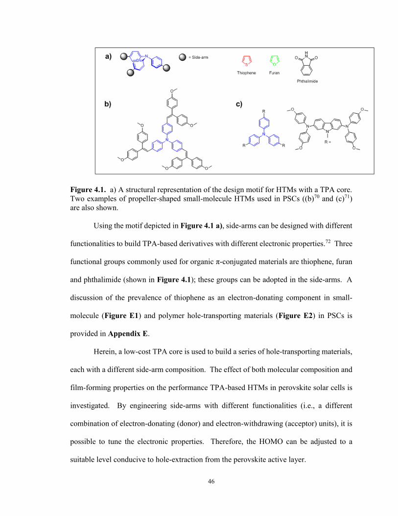
46
Figure 4.1. a) A structural representation of the design motif for HTMs with a TPA core.
Two examples of propeller-shaped small-molecule HTMs used in PSCs ((b)70 and (c)71)
are also shown.
Using the motif depicted in Figure 4.1 a), side-arms can be designed with different
functionalities to build TPA-based derivatives with different electronic properties.72 Three
functional groups commonly used for organic π-conjugated materials are thiophene, furan
and phthalimide (shown in Figure 4.1); these groups can be adopted in the side-arms. A
discussion of the prevalence of thiophene as an electron-donating component in small-
molecule (Figure E1) and polymer hole-transporting materials (Figure E2) in PSCs is
provided in Appendix E.
Herein, a low-cost TPA core is used to build a series of hole-transporting materials,
each with a different side-arm composition. The effect of both molecular composition and
film-forming properties on the performance TPA-based HTMs in perovskite solar cells is
investigated. By engineering side-arms with different functionalities (i.e., a different
combination of electron-donating (donor) and electron-withdrawing (acceptor) units), it is
possible to tune the electronic properties. Therefore, the HOMO can be adjusted to a
suitable level conducive to hole-extraction from the perovskite active layer.

47
4.2. Materials and Methods
4.2.1. Materials
The molecular structures of all organic materials used in this study are given in
Figure 4.2. The molecular formula and molecular weight for each of the materials are
provided in Table 4.1. The first hole-transporting material is 5,5',5''-(5,5',5''-
(nitrilotris(benzene-4,1-diyl))tris(2-hexylthiophene), designated as “HTM01”. HTM01 is
the simplest and smallest molecule in the series with a TPA core flanked by a thiophene
unit for the purpose of extending π-conjugation. The hexyl chains increase solubility in
organic solvents. This compound has been previously synthesized by others via lithiation
and transmetallation.73 In Welch lab, Arthur Hendsbee successfully synthesized HTM01
via direct arylation as an alternative and facile procedure.
The second compound in this study is 5,5',5''-(5,5',5''-(nitrilotris(benzene-4,1-
diyl))tris(furan-5,2-diyl))tris(2-octylisoindoline-1,3-dione), or “HTM02”. HTM02 (also
synthesized by Arthur Hendsbee) has two structural differences compared to HTM01: i)
replacement of the thiophene unit with a furan group and ii) addition of an electron-
deficient phthalimide acceptor group. The furyl units were selected for two reasons. First,
it is considered to be a sustainable and “green” alternative to thiophene as a building block
in functional materials since it is derived from biological feedstocks.74–76 Second,
substitution of furan for thiophene as donor units in organic semiconductors can result in
an increase in hole mobility, as demonstrated by recent work in the Welch and Hill labs77
and by others.78,79 The phthalimide groups are electron-deficient and stabilize the frontier
energy levels of the molecule HTM02 relative to HTM01, resulting in a decrease in the
LUMO energy and a corresponding decrease in the bandgap energy.

48
The third compound is named HTM03. HTM03 is largest, most complex molecule.
Similar to HTM02, HTM03 has furan-phthalimide D-A units. A diketopyrrollopyrrole
(DPP) unit in the center of the side-arm was inserted to stabilize the frontier energy levels,
particularly the LUMO, to reduce the bandgap energy relative to HTM02. Large branched
alkyl chains (i.e., 2-ethylhexyl) help to disrupt strong π-π intermolecular interactions
between DPP units,80 which improves solubility. 1-ethylpropyl or “swallowtail” end caps
were used in place of the hexyl chains present in HTM01 and HTM02.
The fourth hole-transporting material is 7,7’-(4,4-bis(2-ethylhexyl)-4H-silolo[3,2-
b:4,5-b’]dithiophene-2,6-diyl)bis(6-fluoro-4-(5’-hexyl-[2,2’-bithiophen]-5-yl)benzo[c]-
[1,2,5]thiadiazole), which is also known as p-DTS(FBTTh2)2, but is labelled as “HTM04”
throughout this chapter. This material demonstrates high hole-mobility81 and has similar
HOMO energy levels as HTM01, HTM02 and HTM03. For this reason, it is appropriate
for use as a hole-transporting material in this study. HTM04 is also well-known as a high-
performance two-dimensional (2D) donor material in small-molecule organic solar cells.82

49
Figure 4.2. Molecular structures of the five HTMs investigated in this study. The TPA
cores are coloured blue and thiophene units are coloured red.
Table 4.1. The chemical formula and molecular weight of each HTM used in the study.
HTM Chemical Formula Molecular Weight
(g/mol)
HTM01 C48H57NS3 744.17
HTM02 C72H66N4O9 1131.34
HTM03 C147H168N10O18 2263.01
HTM04 C64H72F2N4S8Si 1219.87
Spiro-OMeTAD C81H68N4O8 1225.45
4.2.2. Thin-film Formation via Spin Coating
To characterize each hole-transporting material individually, thin-films were spin-
cast on glass substrates. Precursor solutions were prepared by combining the weighed solid
compound and the measured volume of solvent (chlorobenzene) in a 4.0 mL Teflon-capped
vial with a stir bar. The materials were weighed using an analytical balance and the solvent
was measured using a 1000-μL micropipette. Solutions of spiro-OMeTAD, HTM01 and

50
HTM02 were stirred overnight at RT and solutions of HTM03 and HTM04 were stirred on
a hotplate set to 90 °C.
The 25 mm × 25 mm glass substrates were cut from microscope slides. The
substrates were cleaned prior to use by scrubbing the surface with a mixture of lab detergent
(Sparkleen®) and DI H2O and then rinsing thoroughly with DI H2O. The substrates were
then sequentially rinsed with acetone and ethanol prior to UV/ozone cleaning for 20 min.
Substrates were loaded onto the chuck of a Laurell spin-coater immediately after
UV/ozone treatment. The solutions of spiro-OMeTAD, HTM01 and HTM02 were cast at
RT whereas the solutions of HTM03 and HTM04 were hot-cast due to their lower
solubility. Each solution was retracted from the vial using a 1 mL syringe. Approximately
200 μL of solution was then dispensed onto the center of the substrate through a 0.45 μm
PTFE filter in one aliquot. The spin-coat program was then run using the parameters
specified in Table 4.2. The high solubility of spiro-OMeTAD in organic chlorinated
solvents permits casting from a solution that is higher in concentration than the TPA HTMs
and HTM04.
Table 4.2. HTM deposition parameters.
HTM
Concentration
in CB
(mg/mL)
Solution
Deposition
Temperature
(°C)
Spin Speed
(rpm)
Spin
Duration
(s)
Spiro-OMeTAD 80 25 4000 30
HTM01 25 25 1000 90
HTM02 25 25 1000 90
HTM03 25 70 1000 90
HTM04 25 70 1000 90
4.2.3. PSC Fabrication Procedure
All devices were made with the same architecture: FTO/TiO2
compact/CH3NH3PbI3/HTM/MoO3/Ag. The FTO glass substrates and TiO2 layers were

51
prepared as described in Chapter 3. The perovskite active layers were formed via the
optimal sequential spin-coating method also described in Chapter 3.
After the active layers were converted to perovskite, the devices were removed from
the glovebox. All HTMs were deposited onto the perovskite layer in air via spin-coating
from chlorobenzene solutions and filtered through 0.45 µm PTFE filters. No dopants were
used in the devices comparing the different hole-transporting materials. However, a
detailed discussion of the effect of dopants on HTM performance can be found in
Appendix F with a comparison of JV curves for devices made with doped and undoped
spiro-OMeTAD in Figure F1. Deposition parameters for each HTM are given in Table
4.2. The top metal contact was deposited by thermal evaporation at < 4.0×10⁻⁶ torr in a
custom-built bell-jar evaporation system. A 10-nm layer of molybdenum (VI) oxide
(MoO3) was first deposited followed by 75 nm of Ag. The purpose of using a MoO3-Ag
top contact was to replace the commonly-used Au contact and reduce the overall cost of
the system.83 The final active area of each device was 0.032 cm2.
After fabrication, the devices were promptly transferred into an Ar-filled glovebox,
which was the location for J-V testing and the site of post-testing storage. To account for
hysteresis in the J-V curves, each cell was scanned first from a forward bias (+ 2.0 V) to
short-circuit (0.0 V) and then in the opposite direction. Each scan was repeated with three
different scan delays (5 ms, 10 ms and 100 ms) at a sampling rate of 0.01 V/step.
4.3. Results and Discussion
4.3.1. Material Characterization
Figure 4.3 shows an energy level diagram of the components of the PSC devices.
HOMO and LUMO energy levels of the organic hole-transporting materials were
determined by cyclic voltammetry (CV plots shown in Figure 4.4). The onset of oxidation

52
for each of the HTMs was measured as the intersection of the baseline of the CV plot and
the line tangent to the first oxidation peak. These potential values were referenced to the
oxidation potential of ferrocene, which has been measured previously to be 4.80 eV, and
are listed in Table 4.3.39 Detailed methods for the CV experiments and calculations of the
energy levels can be found in Section 2.7. It was confirmed that the HOMO levels of all
five HTMs were similar (~5 eV) and at an appropriate level for hole-extraction at the
perovskite interface.
Energy levels of the other components are included in the diagram for comparison
and are based on literature reports. The valence band maximum and the conduction band
minimum of the perovskite (CH3NH3PbI3) were previously determined by others.17 The
conduction band minimum of −5.5 eV for an air-exposed film of MoO3 is representative of
n-type MoO3 charge-transport layers used in organic electronic devices.84 In perovskite
solar cells, MoO3 is used as an n-type material to assist charge transfer from the HTMs to
Ag, a high work-function electrode. Dense TiO2 acts as the electron-transport/hole-
blocking layer with a work function of −4.0 eV.85 The work function of fluorine-doped
tin-oxide (FTO), the electron-collecting electrode, is −4.5 eV based on measurements
conducted using X-ray photoelectron spectroscopy (XPS).86
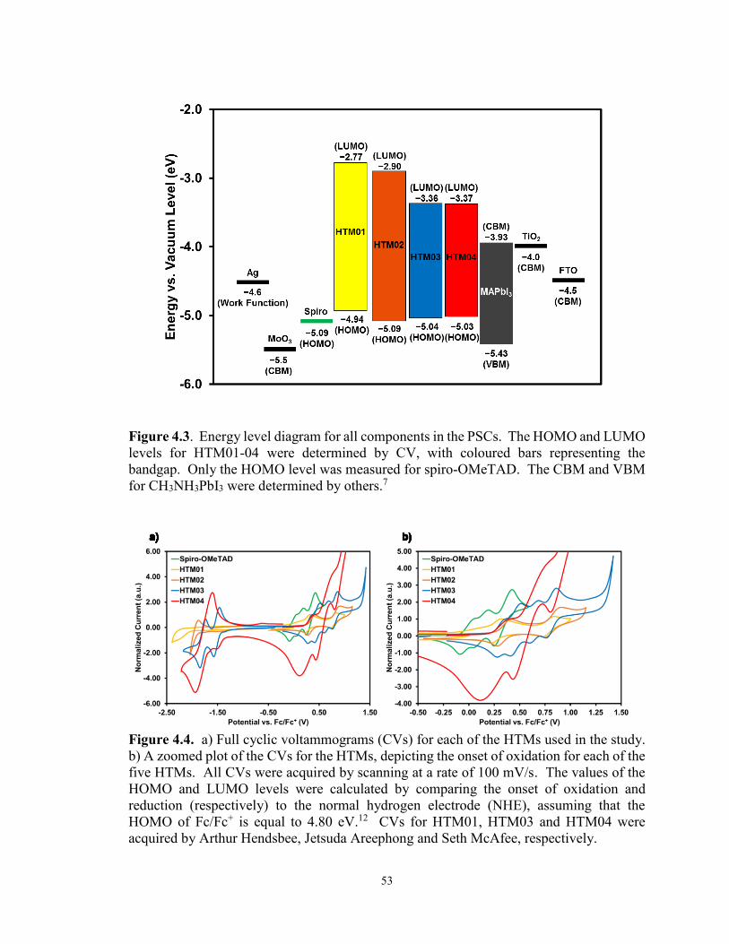
53
Figure 4.3. Energy level diagram for all components in the PSCs. The HOMO and LUMO
levels for HTM01-04 were determined by CV, with coloured bars representing the
bandgap. Only the HOMO level was measured for spiro-OMeTAD. The CBM and VBM
for CH3NH3PbI3 were determined by others.7
Figure 4.4. a) Full cyclic voltammograms (CVs) for each of the HTMs used in the study.
b) A zoomed plot of the CVs for the HTMs, depicting the onset of oxidation for each of the
five HTMs. All CVs were acquired by scanning at a rate of 100 mV/s. The values of the
HOMO and LUMO levels were calculated by comparing the onset of oxidation and
reduction (respectively) to the normal hydrogen electrode (NHE), assuming that the
HOMO of Fc/Fc+ is equal to 4.80 eV.12 CVs for HTM01, HTM03 and HTM04 were
acquired by Arthur Hendsbee, Jetsuda Areephong and Seth McAfee, respectively.
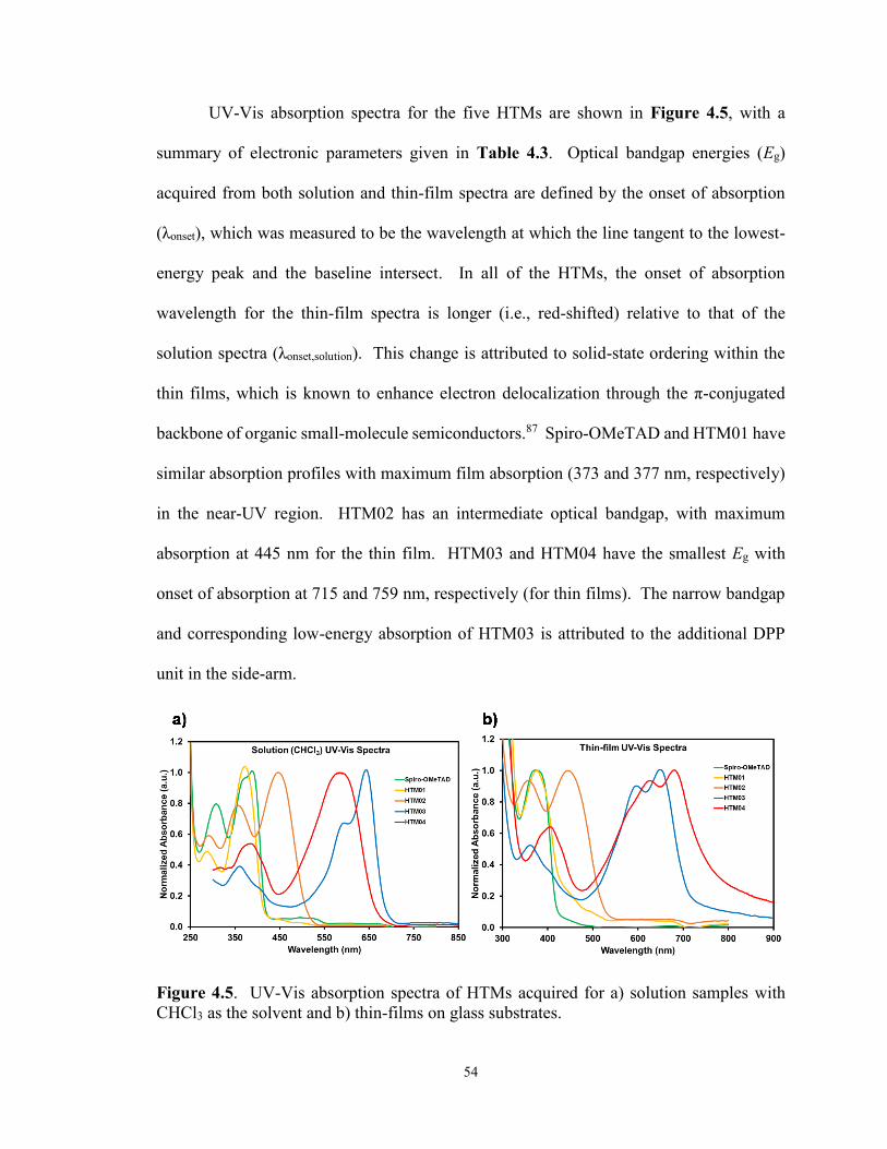
54
UV-Vis absorption spectra for the five HTMs are shown in Figure 4.5, with a
summary of electronic parameters given in Table 4.3. Optical bandgap energies (Eg)
acquired from both solution and thin-film spectra are defined by the onset of absorption
(λonset), which was measured to be the wavelength at which the line tangent to the lowest-
energy peak and the baseline intersect. In all of the HTMs, the onset of absorption
wavelength for the thin-film spectra is longer (i.e., red-shifted) relative to that of the
solution spectra (λonset,solution). This change is attributed to solid-state ordering within the
thin films, which is known to enhance electron delocalization through the π-conjugated
backbone of organic small-molecule semiconductors.87 Spiro-OMeTAD and HTM01 have
similar absorption profiles with maximum film absorption (373 and 377 nm, respectively)
in the near-UV region. HTM02 has an intermediate optical bandgap, with maximum
absorption at 445 nm for the thin film. HTM03 and HTM04 have the smallest Eg with
onset of absorption at 715 and 759 nm, respectively (for thin films). The narrow bandgap
and corresponding low-energy absorption of HTM03 is attributed to the additional DPP
unit in the side-arm.
Figure 4.5. UV-Vis absorption spectra of HTMs acquired for a) solution samples with
CHCl3 as the solvent and b) thin-films on glass substrates.

55
Table 4.3. Summary of optical and electronic parameters of HTMs.
HTM Eox vs.
Fc (V)
EHOMO
(eV)
Eg,solution
(eV)
Eg,film
(eV)
λonset,solution
(nm)
λonset,film
(nm)
Spiro-OMeTAD 0.55 −5.09 2.98 2.96 416 419
HTM01 0.14 −4.94 3.02 2.95 411 420
HTM02 0.26 −5.09 2.43 2.38 510 520
HTM03 0.24 −5.04 1.81 1.73 685 715
HTM04 0.23 −5.03 1.86 1.63 665 759
4.3.2. Perovskite Solar Cell Fabrication and Testing
All devices fabricated without an HTL displayed evidence of shorts and produced
no photocurrent, suggesting that the perovskite layer itself has pinholes – a source of shunt
pathways. On the other hand, all devices with HTLs displayed diode-like J-V curves with
no evidence of shorts (see Figure 4.6). A summary of the device performance metrics for
the best and average cells is provided in Table 4.4. Furthermore, it may be filling-in deep
pinholes in the rough perovskite active layer and may be blocking shunt pathways.
Figure 4.6. J-V curves of the best-performing cells with different HTLs. Also shown is
an illustration of the configuration of the planar PSCs.
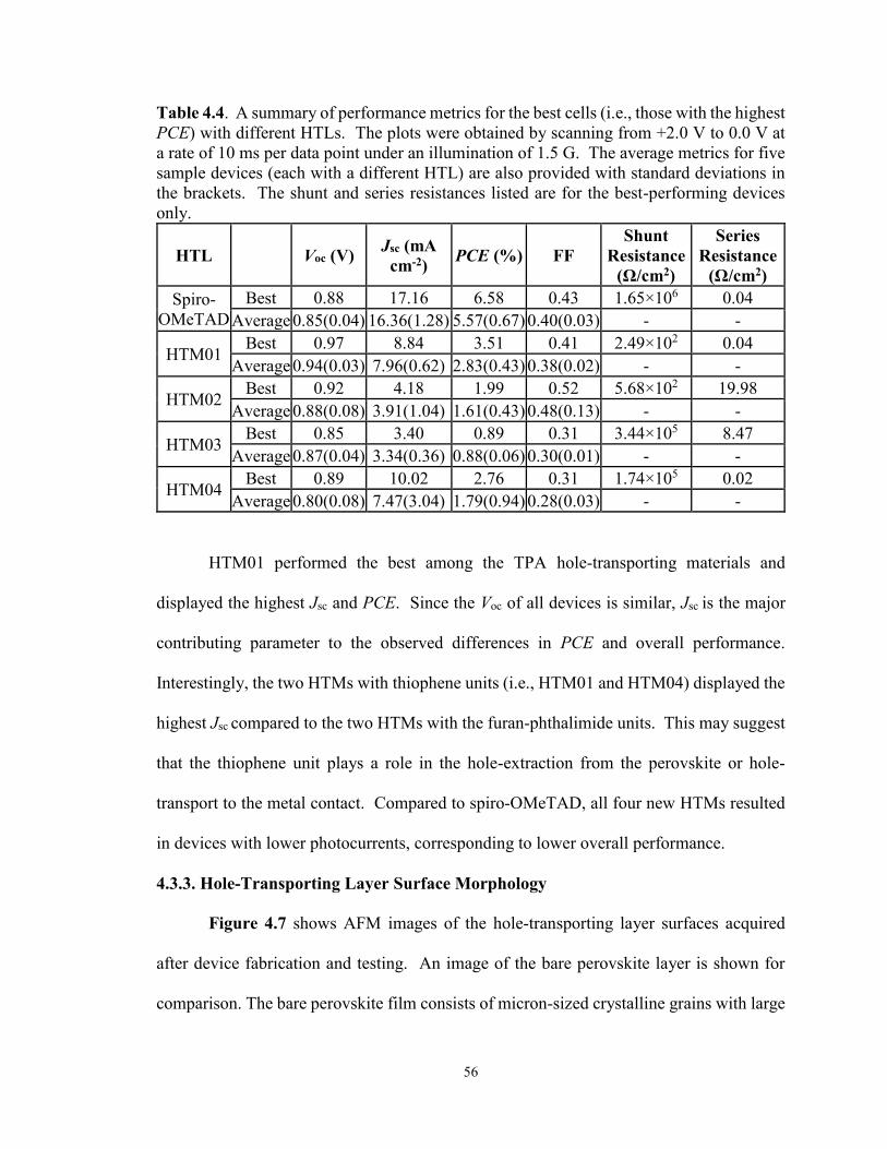
56
Table 4.4. A summary of performance metrics for the best cells (i.e., those with the highest
PCE) with different HTLs. The plots were obtained by scanning from +2.0 V to 0.0 V at
a rate of 10 ms per data point under an illumination of 1.5 G. The average metrics for five
sample devices (each with a different HTL) are also provided with standard deviations in
the brackets. The shunt and series resistances listed are for the best-performing devices
only.
HTL Voc (V) Jsc (mA
cm-2) PCE (%) FF
Shunt
Resistance
(Ω/cm2)
Series
Resistance
(Ω/cm2)
Spiro-
OMeTAD
Best 0.88 17.16 6.58 0.43 1.65×10⁶ 0.04
Average 0.85(0.04) 16.36(1.28) 5.57(0.67) 0.40(0.03) - -
HTM01 Best 0.97 8.84 3.51 0.41 2.49×10² 0.04
Average 0.94(0.03) 7.96(0.62) 2.83(0.43) 0.38(0.02) - -
HTM02 Best 0.92 4.18 1.99 0.52 5.68×10² 19.98
Average 0.88(0.08) 3.91(1.04) 1.61(0.43) 0.48(0.13) - -
HTM03 Best 0.85 3.40 0.89 0.31 3.44×10⁵ 8.47
Average 0.87(0.04) 3.34(0.36) 0.88(0.06) 0.30(0.01) - -
HTM04 Best 0.89 10.02 2.76 0.31 1.74×10⁵ 0.02
Average 0.80(0.08) 7.47(3.04) 1.79(0.94) 0.28(0.03) - -
HTM01 performed the best among the TPA hole-transporting materials and
displayed the highest Jsc and PCE. Since the Voc of all devices is similar, Jsc is the major
contributing parameter to the observed differences in PCE and overall performance.
Interestingly, the two HTMs with thiophene units (i.e., HTM01 and HTM04) displayed the
highest Jsc compared to the two HTMs with the furan-phthalimide units. This may suggest
that the thiophene unit plays a role in the hole-extraction from the perovskite or hole-
transport to the metal contact. Compared to spiro-OMeTAD, all four new HTMs resulted
in devices with lower photocurrents, corresponding to lower overall performance.
4.3.3. Hole-Transporting Layer Surface Morphology
Figure 4.7 shows AFM images of the hole-transporting layer surfaces acquired
after device fabrication and testing. An image of the bare perovskite layer is shown for
comparison. The bare perovskite film consists of micron-sized crystalline grains with large
57
height deviations that resemble “mountains” and “valleys”. Ideally, the HTM would
conform to the rough surface of the perovskite and provide uniform coverage across the
entire active layer. Such morphology would result in devices of consistent HTL thickness,
and therefore, consistent PV performance. It is more likely, however, that the HTM will
tend to planarize the films, partially filling in the low “valleys” while resulting in thinner
coverage on the “mountains”. Herein, AFM was used to assess the morphology of each
HTL in terms of grain size and overall surface roughness.
It is observed that Spiro-OMeTAD forms the smoothest, most planar film over the
underlying perovskite layer with the lowest value of root-mean square roughness (RRMS)
(see Table 4.5). The spiro-OMeTAD solution was also significantly more concentrated
than the others. This may explain how spiro-OMeTAD effectively fills-in gaps between
the large perovskite domains and forms a planar surface over the perovskite crystals. From
the roughness parameters listed in Table 4.5, the roughness of the HTL appears to decrease
from HTM01 to HTM02 to HTM03. Although error bars on the roughness parameters are
not provided, the uncertainty in the values is quite high; the area that was sampled (one or
two 5×5 µm scans per sample) is very small relative to the entire HTL surface.

58
Figure 4.7. 2D AFM images of HTL surfaces of the five hole-transporting materials under
study. An image of a neat perovskite film (i.e., no HTL) is shown for comparison.
Table 4.5. Roughness parameters of HTL films on perovskite films obtained from 2D
AFM images. The parameters were calculated over an area of 25 µm2.
No HTL
(Neat
perovskite)
Spiro-
OMeTAD HTM01 HTM02 HTM03 HTM04
Surface Area (µm²) 26 24 28 24 25 24
RRMS a (nm) 35 12 58 28 17 20
Ra b (nm) 28 10 40 21 13 14
Rmax c (nm) 246 86 445 228 132 170
a RRMS, the root mean square (RMS) average of height deviations relative to the mean image data plane. b
Ra, the average of the absolute values of the surface height deviations relative to the mean plane. c Rmax, the
vertical distance between the highest and lowest data points in the image.
4.4. Conclusions
A design strategy for organic hole-transporting materials has been demonstrated
with applications in PSCs using a TPA-core and highly modular side-arms. By keeping
the HOMO level constant among the HTMs, the effects of shape, size, and conjugation
length on thin-film morphology and device performance could be compared. Following
this approach, the molecular structures of the HTMs could be easily modified, such as the

59
exchange of electron-rich (e.g., thiophene and furan) side-arm functionalities. As a result,
electronic properties such as the HOMO level can be tuned to an appropriate value for hole
extraction from the perovskite. Furthermore, a trend was observed in the performance of
the TPA-based hole-transporting materials and the type of functionalities used in the side-
arms: devices with the HTM including a thiophene unit (HTM01) in the side-arm produced
higher photocurrent than those with HTMs containing the furan-phthalimide unit (HTM02
and HTM03). The bandgap energy of the HTM does not appear to have a significant
influence on PV performance since HTM02 and HTM03 display similar performance, yet
HTM03 has a significantly smaller bandgap. Comparison of the TPA-based donors to
HTM04 confirmed that another thiophene-containing molecule (albeit, linear in shape)
generated greater photocurrent than those with furan-phthalimide. Furthermore, HTM04
has a significantly narrower bandgap than HTM01 yet displays a similar Jsc in PSC devices.
It was shown that the surface roughness of the hole-transporting layer formed by
HTM01, HTM02, HTM03 and HTM04 was not significantly different and therefore was
not a major factor in the observed differences in PV performance. However, it was
observed that spiro-OMeTAD forms a smoother layer than the other four HTMs, which
may be attributed to the high solution concentration. The high solubility of spiro-OMeTAD
gives it the ability to better planarize the rough perovskite film and contributes to the high
PCE.
Development of simple TPA-based hole-transporting materials via facile synthetic
methods is commercially relevant. Having identified a unique structure-performance
relationship, further investigation of the effect of heterocycles in the sidearm units of such
HTMs may proceed. Future optimization in the molecular design of TPA-based HTMs
could focus on adjustments to the side-arm units including:
60
i. The use of sulfur-based heterocyclic functionalities;
ii. Exchanging R-groups (e.g., methoxy) to enhance solubility, affording the
preparation of solutions with higher concentrations, which would lead to
thicker HTL film-formation and better coverage of the perovskite surface.
4.5. Future Work
Two other important factors to consider in the development of alternative HTMs
are air and thermal stability. In order to be viable as a commercial material, the HTM must
be able to operate in humid and at elevated temperatures. For this reason, it is proposed
that the following comparative experiments be conducted for the series of HTMs:
i. Thermogravimetric analysis (TGA) to monitor physical changes to the
materials under heat exposure;
ii. Photovoltaic performance (e.g., J-V) measurements under controlled
atmospheric conditions (e.g., elevated humidity levels).
From this study, it was discovered that the molecular structure of the side-arms of
the TPA-based hole-transporting can influence performance in perovskite solar cells.
Modifications to HTM01 and HTM02 can be made to further investigate the effect of
thiophene, furan, phthalimide and combinations of the three. Figure 4.8 depicts the
molecular structures of two new HTMs. HTM01 is modified by replacing the thiophene
unit with furan, whereas the furan unit in HTM02 is replaced by thiophene while keeping
the phthalimide group present. It is proposed that by fabricating devices with four different
hole-transporting materials under the same, controlled processing conditions, insight into
the relationship of hole-transport in perovskite solar cells and the functional groups in the
HTM can be gathered. This methodology is advantageous with modular designs such as

61
HTM01 and HTM02 since new derivatives can be readily synthesized and screened for
device performance.
Figure 4.8. Proposed modifications to HTM01 and HTM02 for future studies in TPA-
based HTMs.
In a separate study discussed in Appendix G, non-conjugated polymers were
investigated as inert additives in hole-transporting layers of perovskite solar cells. It was
shown that addition of non-conjugated polymers can increase the performance of devices
(Figure G1 for J-V curves) by improving the planarity of the hole-transporting layer
formed by HTM04 (see Figure G2 for AFM images). This strategy is a proposed as a
viable technique to enhance device performance in perovskite solar cells and can be applied
to new TPA-based hole-transporting materials as well.

62
CHAPTER 5 – STAR-SHAPED DONOR MATERIALS FOR SMALL-
MOLECULE ORGANIC SOLAR CELLS
5.1. Background
5.1.1. Transition from Hole-transporting Materials to Donors
It was shown in Chapter 4 that the molecular composition and film-forming properties
of the TPA-based hole-transporting materials can influence device performance in PSCs.
Ultimately, the select TPA-based compounds were not ideal candidates for HTMs – all
three displayed significantly lower performance than spiro-OMeTAD in perovskite solar
cells. However, these materials might be better suited for other photovoltaic applications.
The three newly designed small molecules used as HTMs in PSCs all have appropriate
energy levels and absorption profiles to be considered for use as donor components in
organic solar cells. In some instances, such compounds can serve in both PSC and OSC
devices. For example, in a recent paper by Cheng et al. a single organic compound was
used for the dual-purpose as a hole-transporting material in a perovskite solar cell and as a
donor in a bulk heterojunction organic solar cell.88 Similarly, HTM04 (aka p-
DTS(FBTTh2)2) is a high-performance donor material in OSCs,82,89 but it was shown in
Chapter 4 to also function as an HTM in PSCs.
5.1.2. Selection of a Complementary Acceptor
It is of interest to develop fullerene-free organic solar cells. In small-molecule
organic photovoltaic systems, fullerene derivatives, such as phenyl-C61-butyric acid methyl
ester (PC61BM or PCBM), are the gold-standard electron-acceptors. However, fullerenes
are expensive, difficult to synthesize and display weak absorption of visible light;90,91
factors that are disadvantageous in OSCs. The goal herein is to investigate the new TPA
small molecules as donors with custom-built non-fullerene acceptors.
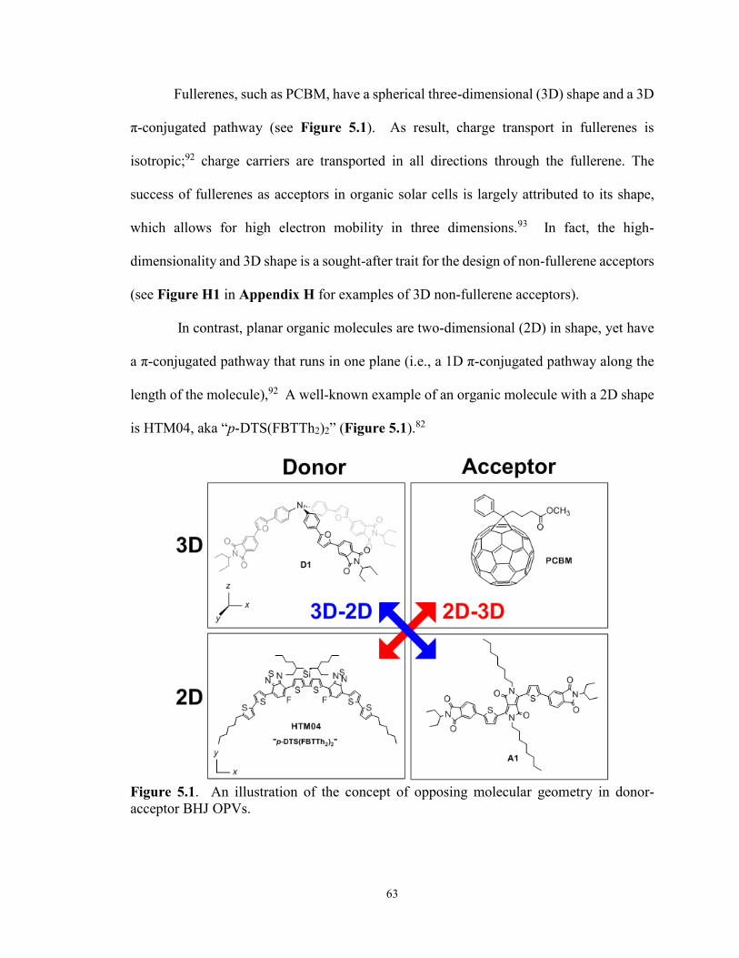
63
Fullerenes, such as PCBM, have a spherical three-dimensional (3D) shape and a 3D
π-conjugated pathway (see Figure 5.1). As result, charge transport in fullerenes is
isotropic;92 charge carriers are transported in all directions through the fullerene. The
success of fullerenes as acceptors in organic solar cells is largely attributed to its shape,
which allows for high electron mobility in three dimensions.93 In fact, the high-
dimensionality and 3D shape is a sought-after trait for the design of non-fullerene acceptors
(see Figure H1 in Appendix H for examples of 3D non-fullerene acceptors).
In contrast, planar organic molecules are two-dimensional (2D) in shape, yet have
a π-conjugated pathway that runs in one plane (i.e., a 1D π-conjugated pathway along the
length of the molecule),92 A well-known example of an organic molecule with a 2D shape
is HTM04, aka “p-DTS(FBTTh2)2” (Figure 5.1).82
Figure 5.1. An illustration of the concept of opposing molecular geometry in donor-
acceptor BHJ OPVs.
64
Some of the best-performing small-molecule OSCs consist of a 3D fullerene
acceptor with a planar 2D donor.94 For clarity, these types of systems will be referred to as
“2D-3D” systems herein (indicated by a red arrow in Figure 5.1). The dissimilarity in
shape between the two complementary materials is thought to drive self-assembly and
produce a solid-state morphology in bulk heterojunction active layer that is conducive to
efficient charge transfer, separation and extraction. These pathways are essential for charge
transportation and collection at the electrodes. Similar to PCBM, TPA-based compounds
also demonstrate high dimensionality and assume a 3D shape. Evidence for the sp3-
hybridization of the N-atom at the TPA core in other related organic semiconductors has
been demonstrated by others using density functional theory (DFT) calculations64 and is
suggested to be the result of steric interactions between the side-arm units.92 As a result,
the molecule assumes a 3D propeller-shape with π-conjugated pathways extending in three
dimensions. To date, all TPA donor materials reported in the literature for use in OSCs are
accompanied with a fullerene acceptor (e.g., C60, PC61BM, PC71BM, etc.), While there
have been some examples in the literature of 3D TPA donors in OSCs achieving modest
PCEs between 3%95–97 and 4%,98 the issue of the use of fullerene acceptors remains
unaddressed.
5.1.3. Custom-Made D-A Pairs
Developing fullerene-free OSCs requires a D-A pair with the following criteria:
i) Distinct geometry/topology to ensure phase separation, allowing for the
formation of homogeneous percolation pathways within the active layer and
charge transport to the electrodes,
ii) Complementary light absorption to maximize photon-harvesting,

65
iii) HOMO/LUMO energy levels that are offset to ensure efficient electron
transfer (LUMO of donor to LUMO of acceptor and HOMO of donor to
HOMO of acceptor),
iv) Thermal and air stability,
v) Low cost with a low embodied energy,
vi) Photo-stability.
The goal herein is to utilize the TPA-based hole-transporting materials developed in
the previous chapter as donor molecules in fullerene-free organic solar cells. It is now
reported how the molecular structure of such compounds will affect the electronic,
structural and morphological properties in thin-film D-A systems. In this case, 3D trigonal
pyramidal conjugated molecules, such as those with a TPA core, are ideally paired with a
planar 2D acceptor to form a “3D-2D” system and satisfy the first criterion (indicated by
the blue arrow in Figure 5.1). Although the geometries of these compounds are agreeable,
the absorption, electronic properties and thin-film morphology must be characterized to
ensure that the other criteria are met.
5.2. Materials and Methods
5.2.1. Materials
Molecules D1, D2 and A1 were synthesized in the Welch lab by Arthur Hendsbee.
The structures of the compounds are depicted in Figure 5.2. The 3D, TPA-based donor
compounds are named “D1” and “D2” for simplicity. The reader is reminded that “D2” is
named “HTM02” in Chapter 4. D1 and D2 differ only in the terminal alkyl chains; D1
has bulky 1-ethylpropyl (aka “swallowtail”) groups while D2 has linear hexyl chains.
A linear, 2D acceptor with a DPP core was selected as the acceptor. This
compound, which is named “A1” for the purpose of this chapter, has been previously
66
reported to have favourable optoelectronic properties for electron transport.99 A1 contains
two bridging thiophene units that connect the DPP core to the electron-deficient
phthalimide end-caps. The terminal and core alkyl groups are swallowtail and octyl chains,
respectively. The design of this compound allows for the substitution of a variety of R-
groups that can influence molecular interactions and self-assembly in the solid-state (vide
infra).
In order to purify the organic compounds used in this work, standard organic
purification techniques were applied by Arthur Hendsbee, including organic extractions,
column chromatography, filtrations and recrystallizations. 1H and 13C nuclear magnetic
resonance (NMR) spectroscopy and mass spectrometry were used to confirm the identity
of the molecules as well as to detect organic impurities. In addition, elemental analysis was
used to confirm the absence of impurities such as inorganic compounds (e.g., SiO2, which
is a potential contaminant during chromatography) that are not visible using other methods.
The samples of each material used herein were qualitatively deemed to be pure when the
analytical methods listed above detected no extraneous signals. It is recognized that this
method of purity assessment is dependent on the detection limit of each instrument.
Although each of the analyses provides a qualitative assessment of sample purity,
quantitative measurements of purity were not conducted.
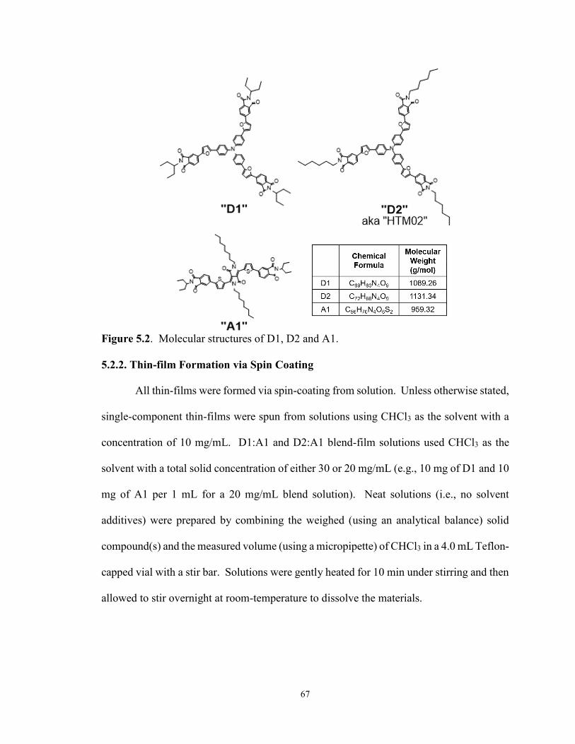
67
Figure 5.2. Molecular structures of D1, D2 and A1.
5.2.2. Thin-film Formation via Spin Coating
All thin-films were formed via spin-coating from solution. Unless otherwise stated,
single-component thin-films were spun from solutions using CHCl3 as the solvent with a
concentration of 10 mg/mL. D1:A1 and D2:A1 blend-film solutions used CHCl3 as the
solvent with a total solid concentration of either 30 or 20 mg/mL (e.g., 10 mg of D1 and 10
mg of A1 per 1 mL for a 20 mg/mL blend solution). Neat solutions (i.e., no solvent
additives) were prepared by combining the weighed (using an analytical balance) solid
compound(s) and the measured volume (using a micropipette) of CHCl3 in a 4.0 mL Teflon-
capped vial with a stir bar. Solutions were gently heated for 10 min under stirring and then
allowed to stir overnight at room-temperature to dissolve the materials.
68
The films were spin-cast using a spin speed of 1000 rpm for a duration of 90 s. A
description of the spin-coating procedure for organic thin-films can be found in Section
4.2.2.
5.2.3. Organic Solar Cell Fabrication Procedure
OSC devices were fabricated on 25 mm × 25 mm pre-patterned ITO-coated glass
substrates. Substrates were cleaned by gently scrubbing the surface with a solution of DI
H2O and Sparkleen® lab detergent using a soft toothbrush. The substrates were then
sonicated vertically in a solution of DI H2O and Sparkleen® for 15 min after which they
were rinsed thoroughly with DI H2O, dried under a stream of filtered air, and then sonicated
vertically in acetone for 15 min. The process was then repeated, but using ethanol as the
solvent. The substrates were then treated under a UV/ozone lamp for 20 min.
Immediately following UV/ozone exposure, a layer of PEDOT:PSS was deposited
as the HTL from a chilled aqueous colloidal suspension purchased from Heraeus (Product:
CleviosTM AI 4083). The substrate was mounted onto the chuck of the spin-coater and
approximately 0.3 mL of the dispersion was dispensed onto the surface through a 0.45 μm
PVDF filter before spinning at 2000 rpm for 45 s. The film was removed at the edges of
the substrate using a lint-free Texwipe® dampened with DI H2O to expose the ITO
contacts. The PEDOT:PSS film was then annealed on a hotplate with a surface temperature
of 140 °C for 10 min. Annealing the PEDOT:PSS film at such temperature has been shown
by others to increase its conductivity, resulting in better-performing devices.100
After cooling the substrates to room-temperature, the active layer was deposited by
spin-coating the surface using blend solutions. The total solids concentration of the
solutions was 20 mg/mL with a 1:1 weight ratio of donor to acceptor, using CHCl3 as the
solvent. For each active layer, 0.2 mL of solution was filtered directly onto the substrate
69
through a 0.45 μm PTFE syringe filter followed by spinning at 1000 rpm for 90 s. The ITO
contacts were then exposed by scraping away the blend film using a razor blade. Once all
active layers were spun, the substrates were promptly cycled into the glovebox and
mounted into a substrate holder with a metal shadow mask.
The top metal contact was deposited using an in-house designed thermal evaporator
equipped with two evaporation sources. Calcium was loaded into an alumina crucible as
the first source and aluminum pieces were secured to a tungsten filament as the second
source. Once the substrates were transferred into the evaporation chamber, the system was
pumped down to <1×10⁻⁶ torr. The metal cathode was formed by sequential thermal
evaporation of 7.5 nm of Ca and 100 nm of Al. The chamber was allowed to cool for 30
min under vacuum before the substrates were transferred directly into the glovebox where
they were promptly tested.
5.2.4. Organic Solar Cell Testing
Device testing was performed using a Keithley 236 Source-Measure Unit in an Ar-
filled glovebox under 100 (±1) mW/cm2 illumination (AM 1.5G). J-V measurements were
collected for each of the 18 devices on each substrate by scanning first from 1.2 V to -0.2V,
1.2 V to -6.2 V and finally from 1.2 V to -0.2 V, at a rate of 0.05 V/step with a delay of 5
ms between steps.
5.3. Results and Discussion, Part I
5.3.1. Materials Characterization, Part I
The first step in the study was to select a suitable solvent for the preparation of thin-
film precursor solutions. Ideally, solutions with high concentrations are preferred for spin-
coating to ensure uniform coverage of the substrate and adequate film thickness (i.e., 100
nm). For this reason, it is favourable to use solvents in which the active materials are highly
70
soluble. The approximate solubility of each of the three materials in three different solvents
with varying polarity (in order of decreasing polarity: ethyl acetate, 2-methyl
tetrahydrofuran, and chloroform (CHCl3)) were determined by an undergraduate honours
student, Liz Kitching. The solubilities were quantified from a calibration curve constructed
using solution UV-Vis data. All three of the materials displayed the highest solubility in
CHCl3. For this reason, all subsequent solutions in this study were prepared using CHCl3
as the solvent.
UV-Vis absorption spectra for the three materials are plotted in Figure 5.3 a). The
absorption profiles of D1 and D2 are almost identical. This can be explained by the
structural similarity of the two materials; both contain the same light-absorbing π-
conjugated backbone. The absorption of A1 extends to longer wavelengths than both of
the donor materials and is reflective of its narrow bandgap. This can be explained by the
presence of the DPP chromophore; electrons are localized in low-lying molecular orbitals
at the DPP core,101 and low-energy photons are sufficient to induce electronic transitions.
By combining either D1 or D2 with A1, the materials absorb across a broad range of the
visible-light spectrum, fulfilling the second criteria for a D-A pair: complementary light
absorption.
The CV plots for the three materials are shown in Figure 5.3. As expected, D1 and
D2 exhibit very similar CVs, owing to their similar molecular structures. The oxidation
potentials of both donor compounds are well-defined by the sharp oxidation peaks,
allowing accurate elucidation of the HOMO levels. The bandgap energies (Eg,CV) for each
of the materials are listed in Figure 5.3 d) and were obtained by taking the difference
between the calculated HOMO and LUMO energy levels. These values are in good
agreement with the values of the bandgap (Eg,onset) that were measured from the UV-Vis
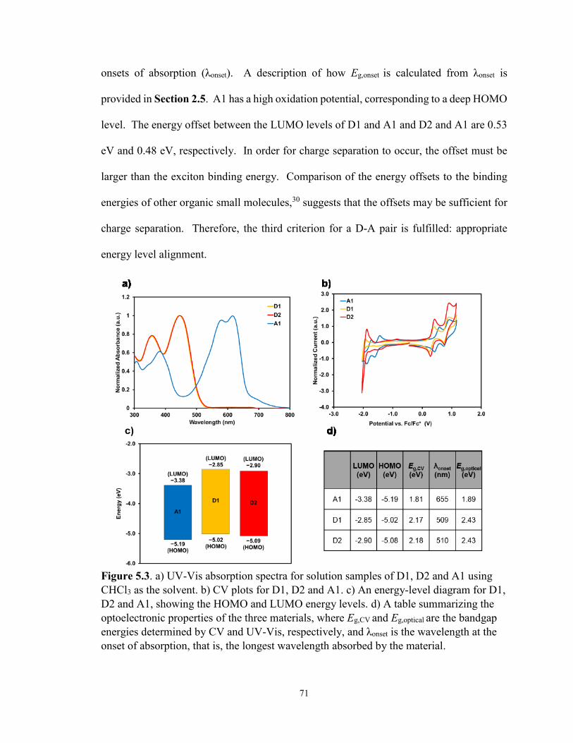
71
onsets of absorption (λonset). A description of how Eg,onset is calculated from λonset is
provided in Section 2.5. A1 has a high oxidation potential, corresponding to a deep HOMO
level. The energy offset between the LUMO levels of D1 and A1 and D2 and A1 are 0.53
eV and 0.48 eV, respectively. In order for charge separation to occur, the offset must be
larger than the exciton binding energy. Comparison of the energy offsets to the binding
energies of other organic small molecules,30 suggests that the offsets may be sufficient for
charge separation. Therefore, the third criterion for a D-A pair is fulfilled: appropriate
energy level alignment.
Figure 5.3. a) UV-Vis absorption spectra for solution samples of D1, D2 and A1 using
CHCl3 as the solvent. b) CV plots for D1, D2 and A1. c) An energy-level diagram for D1,
D2 and A1, showing the HOMO and LUMO energy levels. d) A table summarizing the
optoelectronic properties of the three materials, where Eg,CV and Eg,optical are the bandgap
energies determined by CV and UV-Vis, respectively, and λonset is the wavelength at the
onset of absorption, that is, the longest wavelength absorbed by the material.
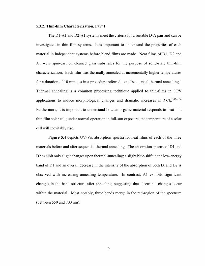
72
5.3.2. Thin-film Characterization, Part I
The D1-A1 and D2-A1 systems meet the criteria for a suitable D-A pair and can be
investigated in thin film systems. It is important to understand the properties of each
material in independent systems before blend films are made. Neat films of D1, D2 and
A1 were spin-cast on cleaned glass substrates for the purpose of solid-state thin-film
characterization. Each film was thermally annealed at incrementally higher temperatures
for a duration of 10 minutes in a procedure referred to as “sequential thermal annealing.”
Thermal annealing is a common processing technique applied to thin-films in OPV
applications to induce morphological changes and dramatic increases in PCE.102–104
Furthermore, it is important to understand how an organic material responds to heat in a
thin film solar cell; under normal operation in full-sun exposure, the temperature of a solar
cell will inevitably rise.
Figure 5.4 depicts UV-Vis absorption spectra for neat films of each of the three
materials before and after sequential thermal annealing. The absorption spectra of D1 and
D2 exhibit only slight changes upon thermal annealing; a slight blue-shift in the low-energy
band of D1 and an overall decrease in the intensity of the absorption of both D1and D2 is
observed with increasing annealing temperature. In contrast, A1 exhibits significant
changes in the band structure after annealing, suggesting that electronic changes occur
within the material. Most notably, three bands merge in the red-region of the spectrum
(between 550 and 700 nm).

73
Figure 5.4. UV-Vis absorption spectra acquired by Liz Kitching for neat films of a) D1,
b) D2 and c) A1 during the sequential thermal annealing experiment. The absorption
spectrum was first acquired for each as-cast film. Each film was then annealed by placing
the substrate onto a hotplate heated at 100 °C for 10 min after which a second absorption
spectrum was acquired. This process was repeated, sequentially annealing at incrementally
higher temperatures.
Thin-film blends of D1 and A1 and D2 and A1 were spin-cast on glass substrates
by Liz Kitching. Similar to the one-component films, sequential thermal annealing was
applied to the blend films and UV-Vis absorption spectra acquired after each annealing
step. The absorption spectra of the blend films are depicted in Figure 5.5.
Figure 5.5. UV-Vis absorption spectra acquired for blend films of a) D1-A1 and b) D2-
A1 during the sequential thermal annealing experiment. Solutions for both blends were
prepared using the donor and acceptor compounds in 1-to-1 weight ratios.

74
The spectra of both unannealed (i.e., as-cast) blend films reveal two distinct bands
in the region between 550 and 700 nm that are absent in the A1 as-cast neat film (see Figure
5.3 c)). The resolution of these bands suggests that the presence of the donor influences
the solid-state ordering of A1 in the thin-film blend. Similar to the phenomenon observed
in the neat film of A1, thermal annealing results in a change in the band structure of A1
within both blend films; three bands emerge upon annealing. From the UV-Vis spectra in
Figure 5.4, it is clear that the absorption of the donor and acceptor is unbalanced in the
blend films; the magnitude of absorption of D1 and D2 is considerably greater than that of
A1. For this reason, blends with higher quantities of A1 relative to the donor were
investigated. UV-Vis spectra (Figure I1) and XRD powder patterns (Figure I2) for films
with varying ratios of donor and acceptor are provided in Appendix I.
The interactions between the donors and A1 within the blend films were further
probed using photoluminescence (PL) spectroscopy (Figure 5.6). In this experiment, the
thin film samples were irradiated with monochromatic light of a wavelength, λex. A
photodetector collected the emitted light across a range of wavelengths (λem), providing
evidence for fluorescence. PL spectra of D1 and D2 neat films were first acquired using
an excitation wavelength of 443 nm and collecting emitted radiation from 500 to 900 nm.
The A1 neat film displayed minimal fluorescence when excited at the wavelength of
maximum absorbance (i.e., 587 nm). For this reason, the PL spectrum of A1 is not shown.

75
Figure 5.6. PL spectra comparing the fluorescence of one-component donor films with
two-component donor-acceptor (1:1 weight ratio) blend films.
As illustrated in Figure 5.6 a) and b), both D1 and D2 exhibit significant
fluorescence in single-component samples. That is, the electrons are effectively excited
from the LUMO to the HOMO and subsequently relax to the ground state, emitting a photon
in the process. However, the blend films with equal quantities of donor and acceptor
display negligible fluorescence. This indicates that the exciton dissociates at the D-A
interface, separating into free charge carriers. The electrons are effectively transferred from
D1 or D2 to A1, and are provided with alternate relaxation pathways. As a result, electrons
do not relax from the LUMO to the HOMO of the donor and the intensity of the
fluorescence is reduced or “quenched”. PL quenching provides additional evidence for D-
A interactions within the blends, which is a favourable trait for materials in organic solar
cells.
Thus far, all experiments described were conducted on both D1-A1 and D2-A1
systems in parallel. For the purpose of streamlining the optimization of thin-films for
application in organic solar cells, one system is subsequently studied in greater depth.
Since D1 and A1 have identical alkyl end-caps (i.e., swallowtail), which suggests molecular
compatibility, the D1-A1 system was selected for further optimization.

76
It is important to consider the crystallinity of the materials within the active layer;
formation of well-ordered crystalline domain can enhance charge transport.105 The changes
in the absorption profiles of the blend films induced by thermal annealing (see Figure 5.5)
are indicative of electronic changes that may be related to the crystallinity or solid-state
ordering of the materials. To further probe the structure of the films, XRD experiments
were conducted. XRD patterns of thin films of D1 and A1 are shown in Figure 5.7 a) and
b), respectively, and are compared to a two-component blend film (1:1 weight ratio of D1
and A1, Figure 5.7 c)) before and after annealing at an intermediate temperature (150 °C).
Figure 5.7. XRD patterns of one-component thin-films of a) D1 and b) A1 and c) a two-
component D1-A1 blend film acquired before and after thermal annealing for 120 min at
150 °C. The scans were acquired with a range between 3° and 20°, however, no diffraction
peaks were observed above 2θ = 10°. Thus, only narrow range is used to clearly the show
the peaks.
Based on the absence of diffraction peaks for any of the as-cast films, it is assumed
that the materials are amorphous within the films or consist of sub-nanometre grains. Upon
annealing, the pattern of D1 does not change; no diffraction peaks are observed in the as-
cast nor the annealed film, indicating that the material remains amorphous. However, a
single diffraction peak is observed for the A1 film at 2θ = 4.3° after annealing – an
indication of solid-state ordering. After annealing the blend film, a peak emerges at the
same position as in the A1 film, indicative of crystallization of A1 domains.

77
In a separate experiment, the effect of annealing temperature on crystallinity of the
blends is illustrated by comparing XRD patterns of films annealed at 150 °C and at 180 °C
(see Figure 5.8). Annealing at a higher temperature results in a diffraction peak at the same
angle as the film annealed at 150 °C and of the annealed A1 film. This suggests that A1
assumes the same crystalline phase regardless of the annealing temperature. However, the
film annealed at high temperature displays a peak of higher-intensity; an indication of the
growth of larger crystallites.
Figure 5.8. XRD patterns of separate films of D1-A1 blends (1:1 weight ratio) comparing
the effect of annealing temperature on crystallinity. The films were annealed for 30 minutes
at either 150 or 180 °C.
5.3.3. Organic Solar Cell Testing, Part I
Based on the differences in the absorption spectra (Figure 5.5) and XRD patterns
(Figure 5.7 and 5.8) of the blend films, it is clear that electronic and structural changes
occur upon thermal annealing. To determine the effect of thermal annealing on PV
performance, OSCs were fabricated on three separate substrates using D1:A1 active layers
employing a conventional device architecture (see Figure 5.9 b)). A detailed fabrication
procedure can be found in Section 5.2.5. Before deposition of the metal cathode, each

78
substrate was annealed on a hotplate in the glovebox at a different temperature (or tested
without annealing).
All devices displayed linear J-V curves, with very high series resistance and very low
Jsc. Regardless of annealing condition, very little photocurrent was generated suggesting
that the system was not operational in OSC devices.
Figure 5.9. a) J-V curves of representative devices with D1-A1 active-layer blends in a
1:1 ratio. b) An illustration of the layered “conventional”-style architecture. c) A table of
performance metrics. d) Photographs of the completed devices.
To gain insight into the cause of the poor device performance, AFM images of the
active layers were acquired after device testing (Figure 5.10). The images reveal the
topography of the active layer surfaces and allow for quantification of the domain sizes.
The as-cast film consists of very small domains with minimal phase-separation. Annealing
at 150 °C induces growth of larger features that are likely crystalline domains of A1 which
correspond to the diffraction peak observed in the XRD pattern. The film annealed at 180
°C consists of large columnar crystallites up to a micron in breadth. These images correlate

79
well with the XRD patterns and confirm the growth of larger crystallites upon high-
temperature annealing. The large features observed in the images of the annealed films are
likely crystalline domains of A1.
Figure 5.10. 2D AFM images of the D1:A1 active-layer surfaces of the OSC devices.
5.3.4. Conclusions, Part I
The binary blend of D1 and A1 was determined to be a poor system for use in
organic solar cells. Despite evidence for PL quenching (Figure 5.6), and therefore
molecular compatibility as a D-A pair, preliminary devices performed poorly.
AFM reveals very different morphologies between as-cast and annealed films, none
of which are likely to display good performance as the active layer in OSCs. Based on the
AFM and XRD data, it can be concluded that: i) the amorphous nature of the as-cast films
consists of few charge-transport or percolation pathways and ii) the over-crystallization of
A1 upon annealing forms domains that are too large for efficient charge generation.
For this system, control of the D-A film morphology was used as a strategy to
improve the PV performance. Two strategies that can be used to influence the film

80
morphology are: i) solution-processing techniques and ii) molecular engineering. Two
examples of solution-processing techniques are the addition of solvent additives and
solvent-vapour annealing (SVA). In a preliminary study described in Appendix J, it was
observed that addition of solvent additives (Figure J1) and solvent-vapour annealing
(Figures J2 and J3) modifies the absorption properties of the materials. However, the
focus of the project herein is to apply a molecular design strategy to tune the self-assembly
of the acceptor and enhance the morphology of the thin films.
5.4. Results and Discussion, Part II
5.4.1. New Acceptors: A Molecular Design Strategy
Moving forward, the unfavourable over-crystallization of the acceptor was
addressed through molecular design. The molecular structure of the 2D acceptor was
modified to influence its self-assembly within the thin film. D1 continued to be used as the
donor in the system for its 3D shape and amorphous nature.
One of the simplest approaches to changing the self-assembly and crystallinity of
A1 is by modifying the alkyl chains, taking advantage of the facile synthetic procedure and
infinite tunability of this molecular framework. By substituting different alkyl chains for
the octyl and swallowtail groups at the central and terminal positions of A1, respectively,
the solid-state self-assembly can be controlled to change the morphology of the resulting
thin films. Following this approach, another graduate student researcher in the Welch lab,
Arthur Hendsbee, synthesized a series of derivatives of A1 (Figure 5.11), each with
different functional units and/or alkyl chains (Table 5.1). Each derivative was designed to
be less crystalline than A1 to avoid the large-domain phase separation observed in the D1-
A1 system (recall Figure 5.10). Since the major driving force for crystallization in π-

81
conjugated materials is π-π interactions between adjacent molecules, side chains were
selected to disrupt the π-π interactions and reduce the tendency to crystallize.
Figure 5.11. Molecular structures of A1 and the four new acceptor derivatives.
Table 5.1. Molecular components used in the acceptor derivatives.
Central R-groups Terminal R-group End-Cap Unit
A1 Octyl 1-Ethylpropyl Phthalimide
A2 2-Ethylhexyl 1-Ethylpropyl Phthalimide
A3 2-Ethylhexyl Octyl Phthalimide
A4 Octyl Octyl Napthalimide
A5 2-Hexyldecyl Octyl Phthalimide
Similar to A1, A2 has terminal swallowtail R-groups, but has a branched 2-
ethylhexyl chain stemming from the DPP core as opposed to the linear octyl chains on A1.
A3 differs from A2 with the substitution of the swallowtail groups for octyl chains. The
bulky branched chains at the core are expected to increase the spatial separation of the DPP
units of adjacent molecules thereby weakening the π-π interactions and reducing the
tendency to crystallize. In comparison, the linear octyl chains of A1 display strong van der
Waals forces, which drive the molecules into a stacking crystalline arrangement. Similar
to A3, A5 has terminal octyl chains, but larger branching central groups (2-hexyldecyl).

82
A4 is unique with larger naphthalimide groups as the terminal electron-withdrawing units
in place of phthalimide. Compared to phthalimide, naphthalimide groups induce a greater
torsional strain within the π-conjugated backbone, resulting in a less-planar molecule and
weaker π-π interactions.
5.4.2. Materials Characterization, Part II
To determine if each of the new acceptors is electronically-compatible with D1, CV
experiments were conducted and the HOMO and LUMO energy levels were calculated
based on the oxidation and reduction potentials, respectively. A description of how the
energy levels were calculated is provided in Section 4.3.1. The energy level diagram in
Figure 5.12 a) shows the relative positions of the frontier molecular orbitals compared to
those of D1. Normalized CV plots are provided in Figure 5.12 b). The similar energy
levels of the all five acceptors can be explained by the similar conjugated backbone
structure.
Figure 5.12. a) Energy levels of the frontier molecular orbitals of D1 and the five acceptors
determined by CV. The coloured bars represent the bandgaps of each material. b) CV
plots for the acceptor derivatives, normalized such that the current of the first oxidation
peak is set to unity. The onsets of oxidation and onset of reduction for each material were
used to determine the HOMO and LUMO energy levels, respectively. Each CV was
acquired by scanning at a rate of 100 mV/s.

83
5.4.3. Thin-film Characterization, Part II
Thermal annealing was applied to thin-film blends of D1-Ax systems as a
processing technique. The high-temperature condition (i.e., 180 °C) was selected to gain
insight into the robustness of the system against crystallization. UV-Vis spectra were
acquired on two separate films of each blend: i) one unannealed film and ii) a different film
annealed at 180 °C for 10 min after spin-casting. All films were spin-cast onto glass
substrates from CHCl3 solutions at concentrations of 20 mg/mL with a donor:acceptor
weight ratio of 1:1 (D1:Ax).
The UV-Vis absorption spectra are compared in the left-hand column of Figure
5.13. For all unannealed/as-cast blend films, the absorption of D1 (350-500 nm) is
considerably more intense than the absorption attributed to the acceptor (550-700 nm).
Significant changes in the absorption profiles of the blends with A2 and A3 are observed
after annealing (Figure 5.13 b) and c), respectively). For the D1-A2 blend, three notable
changes occur with annealing. First, the two high-energy bands attributed to D1 are blue
shifted, similar to what is observed in the D1-A1 blend. Second, a third band is observed
in the A2 region, increasing the overall breadth of the absorption. Third, there is an overall
relative increase in intensity of the low-energy absorption.
For the D1-A3 film, there is a large red-shift in the low-energy (A3) absorption
upon annealing. The two bands also become more distinct with a greater energy-separation.
Like A2, a third low-intensity absorption band emerges at the high-energy (blue) end of
absorption (580 nm). Also worthy of note is a blue-shift in the low-energy band of D1
from 445 to 425 nm.
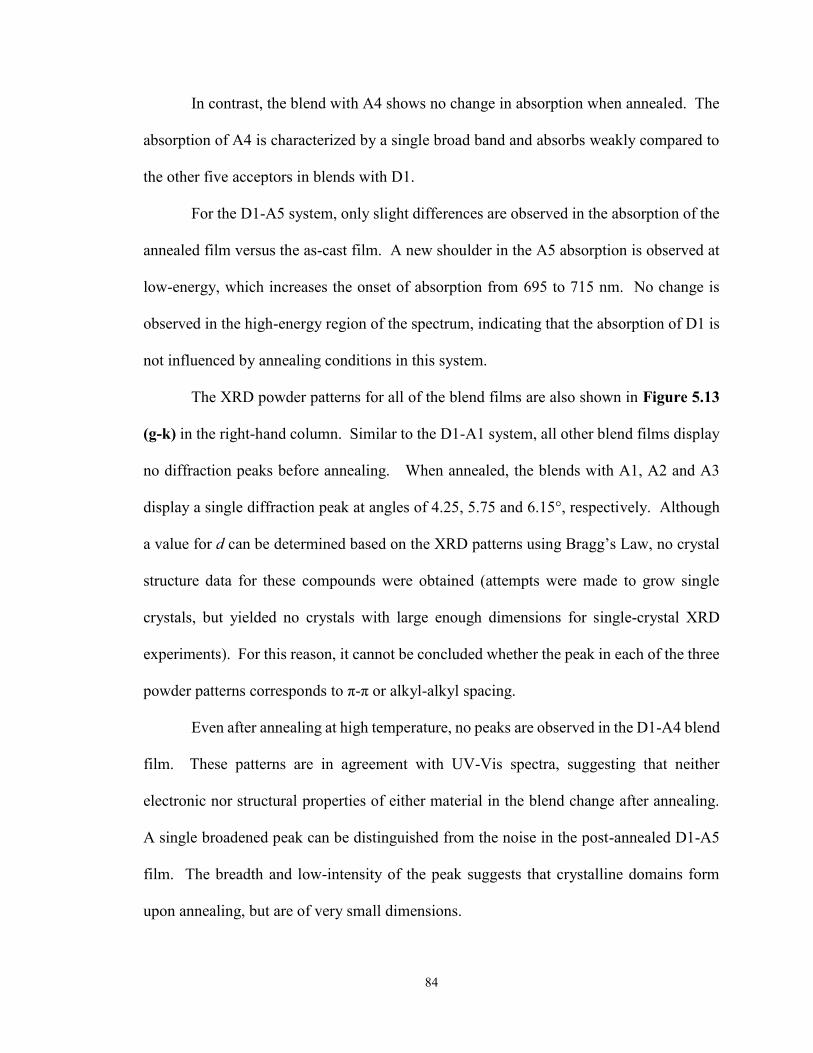
84
In contrast, the blend with A4 shows no change in absorption when annealed. The
absorption of A4 is characterized by a single broad band and absorbs weakly compared to
the other five acceptors in blends with D1.
For the D1-A5 system, only slight differences are observed in the absorption of the
annealed film versus the as-cast film. A new shoulder in the A5 absorption is observed at
low-energy, which increases the onset of absorption from 695 to 715 nm. No change is
observed in the high-energy region of the spectrum, indicating that the absorption of D1 is
not influenced by annealing conditions in this system.
The XRD powder patterns for all of the blend films are also shown in Figure 5.13
(g-k) in the right-hand column. Similar to the D1-A1 system, all other blend films display
no diffraction peaks before annealing. When annealed, the blends with A1, A2 and A3
display a single diffraction peak at angles of 4.25, 5.75 and 6.15°, respectively. Although
a value for d can be determined based on the XRD patterns using Bragg’s Law, no crystal
structure data for these compounds were obtained (attempts were made to grow single
crystals, but yielded no crystals with large enough dimensions for single-crystal XRD
experiments). For this reason, it cannot be concluded whether the peak in each of the three
powder patterns corresponds to π-π or alkyl-alkyl spacing.
Even after annealing at high temperature, no peaks are observed in the D1-A4 blend
film. These patterns are in agreement with UV-Vis spectra, suggesting that neither
electronic nor structural properties of either material in the blend change after annealing.
A single broadened peak can be distinguished from the noise in the post-annealed D1-A5
film. The breadth and low-intensity of the peak suggests that crystalline domains form
upon annealing, but are of very small dimensions.
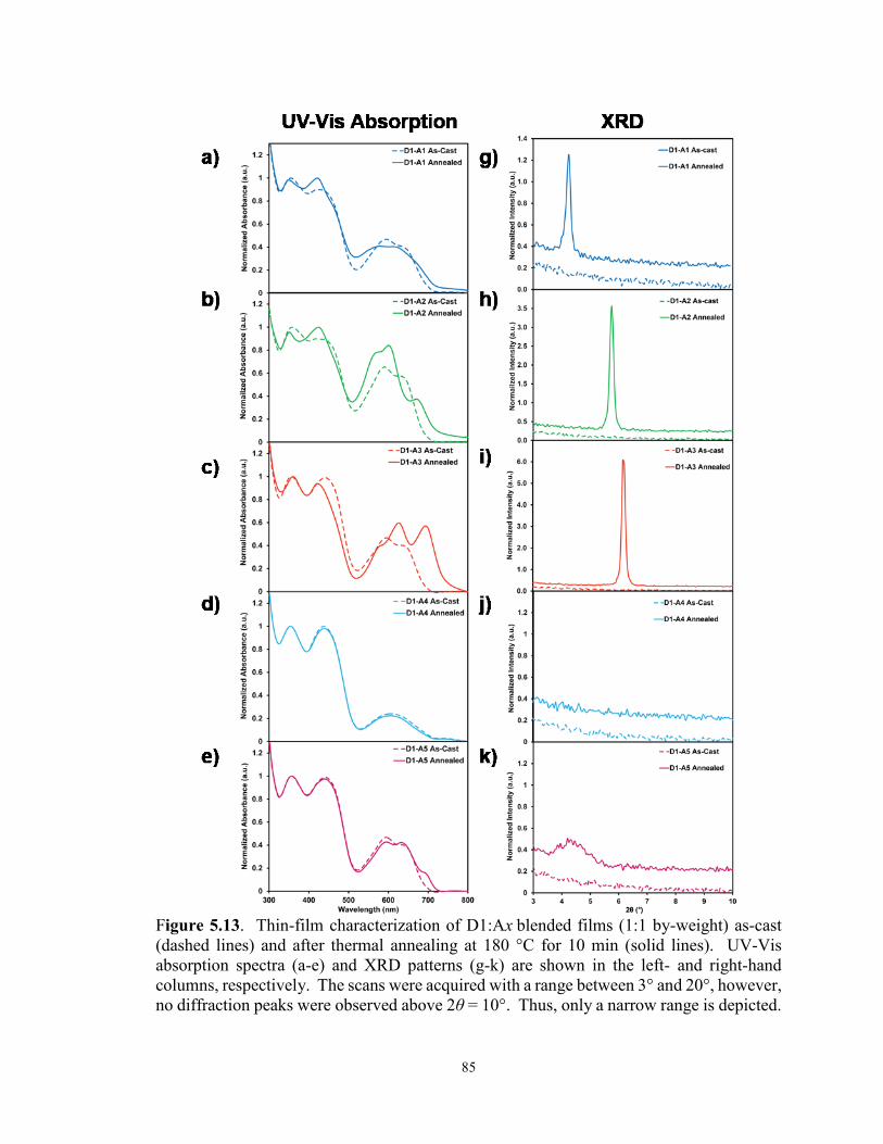
85
Figure 5.13. Thin-film characterization of D1:Ax blended films (1:1 by-weight) as-cast
(dashed lines) and after thermal annealing at 180 °C for 10 min (solid lines). UV-Vis
absorption spectra (a-e) and XRD patterns (g-k) are shown in the left- and right-hand
columns, respectively. The scans were acquired with a range between 3° and 20°, however,
no diffraction peaks were observed above 2θ = 10°. Thus, only a narrow range is depicted.
86
The AFM images reveal the morphology of the thin-film blends and are shown in
Figure 5.14. When unannealed, all blend films display a featureless morphology with no
indication of phase separation; this is in agreement with the lack of diffraction peaks in the
XRD patterns. Similar to the D1-A1 blend (shown again in Figure 5.14 for comparison),
the D1-A2 and D1-A3 blends develop large crystalline domains upon annealing. The D1-
A2 annealed blend consists of large mountainous domains measuring microns in lateral
dimension, with height deviations up to 200 nm. The D1-A3 blend has smaller, more-
compact pebble-like features.
The annealed film of the D1-A4 blend becomes more textured after annealing;
however, the features are very small. Based on the lack of diffraction peaks in the XRD
pattern (Figure 5.13 j)) these features are likely to be amorphous or too small to result in
diffraction peaks. Similar to the blend with A4, the A5 blend film roughens upon annealing
with large waves spanning microns across the substrate. The roughening is likely formation
of the crystalline domains that give rise to the broadened diffraction peak observed in the
XRD pattern in Figure 5.13 k).
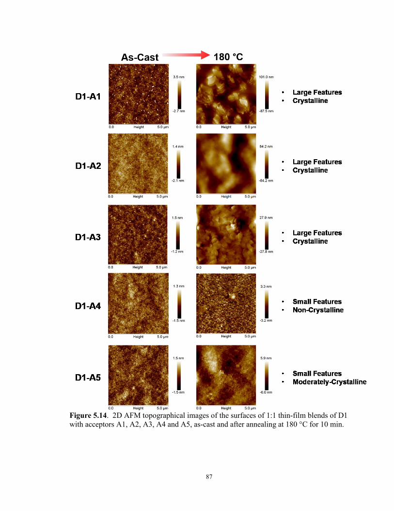
87
Figure 5.14. 2D AFM topographical images of the surfaces of 1:1 thin-film blends of D1
with acceptors A1, A2, A3, A4 and A5, as-cast and after annealing at 180 °C for 10 min.

88
5.4.4. Organic Solar Cell Testing, Part II
To compare the PV performance of each new donor-acceptor system as the active
layer in OSCs, a batch of devices was fabricated on five different substrates with a
conventional device architecture. The fabrication procedure is outlined in Section 5.2.5.
The metal cathode was deposited onto the unannealed (i.e., as-cast) active layers. All
devices were tested as-cast and then annealed on a hotplate at 180 °C for 10 min in the
glovebox before re-testing the annealed devices. The J-V curves of all devices were linear
with very high series resistance and minimal current; no effect was observed from
annealing. However, only one batch of devices was made for these D-A combinations.
Since the control devices with (p-DTS(FBTTh2)2 and PCBM as the donor and acceptor,
respectively) had poorer PCEs than in previous batches, it is possible that other materials
in the cells (e.g., PEDOT:PSS) could have been defective.
5.4.5. Conclusions, Part II
In Part II of this project, it was demonstrated that molecular design (e.g., R-groups
and naphthalimide units) influences the electronic and film-forming properties of a series
of DPP-based small-molecule derivatives paired with a 3D TPA-based donor.
Based on the absorption spectra, XRD and AFM images, conclusions can be drawn
about the effect of R-groups on the self-assembly the materials within solid-state thin-film
blends. Among the five acceptor derivatives studied, A1, A2 and A3 clearly respond to
heat most significantly as indicated by i) changes in the absorption properties (UV-Vis),
and ii) development of large crystalline domains (XRD and AFM) upon annealing. These
conditions are not favourable for organic photovoltaic applications – the morphology needs
to be robust and resistant to heat in functional solar cells since the cells will increase in
temperature during regular cell operation under full-sun exposure.

89
In contrast, the solid-state ordering of A4 appears to be quite resistant to heat. It
can be speculated that the substitution of the napthalimide unit for phthalimide reduces the
ordering of the molecules and is responsible for the lack of crystallinity in the film.
However, the lack of order in the thin-film may not be ideal; if no ordered domains exist,
charge-transport pathways will not be formed and no current will be generated by the cell.
In this case, charge-mobility measurements would be needed for confirmation.
A5 exhibits the “best-of-both-worlds” scenario: the film is amorphous as-cast, but
develops crystalline networks once annealed at high-temperature; a processing condition
that can easily be implemented into the fabrication of cells on an industrial scale. These
properties suggest that the blend contains charge-transporting percolation networks and that
the morphology and electronics will remain in-tact under normal cell operation.
5.5. Outlook and Future Work
Ultimately, fabrication employing each of the blends using a conventional-style
architecture yielded non-functional organic solar cell devices. The reason for the poor
performance and low current is unknown based on the current data. Nevertheless, several
approaches exist for troubleshooting non-functioning systems:
i) Device engineering – investigating alternative device architectures. For
example, other members of the Hill lab have discovered that “inverted” solar
cell designs can perform better than conventional cells when using the same
active layer blends.
ii) Applying additional experimental techniques to further characterize the blends
and provide a better understanding of the materials. For example, charge-
transport properties of the materials (e.g., hole-mobility) of D1 and D2 by
fabricating thin-film transistors (TFTs) are important to understanding the cause

90
of the low photocurrents generated by the preliminary devices. It is also of
interest to investigate the thermal stability of the materials using TGA,
especially when high-temperature annealing is used as a processing technique.
These data are also relevant to the application of D2/HTM02 as the hole-
transporting layer in PSCs (Chapter 4).
iii) Synthesizing more acceptor derivatives with different R-groups. The organic
semiconductors presented in this study are infinitely tunable – using the results
gathered in this study and the trends observed in the effect of side-chain
engineering on the electronic and structural properties, efforts can now be
focused on derivatives with the best properties. For example, it has been shown
that branched chains at the DPP core effectively reduce crystallinity and domain
sizes in solid-state thin films.
iv) Continuing to optimize processing conditions of the existing materials to tune
the blend properties. This strategy includes the application of techniques such
as solvent additives, solvent vapour annealing and inert polymer additives.
Preliminary investigations of solvent additives and solvent vapour annealing
were performed and are discussed in Appendix J.
v) Substitution of other functionalities. For example, A1 has three types of
functional units: i) DPP, ii) thiophene and iii) phthalimide. Each of these units
can be replaced by analogous units (e.g., furan) that can alter both the electronic
properties (e.g., absorption, bandgap, etc.) and self-assembly (e.g., d-spacing,
crystallinity, domain sizes, etc.).
While each of these five possible directions holds promise, strategies iv) and v) were
selected while continuing to work with similar materials. It is clear that the DPP-based

91
compounds demonstrate interesting electronic and structural responses to processing
conditions. For this reason, a related compound (i.e., AX in Figure 5.15) was selected as
an electron donor paired with a promising non-fullerene acceptor. Strategies outlined in
iv) were applied to this new system. Solution-processing techniques were shown to change
the electronic, structural and morphological properties of thin-films and could be used to
enhance device performance when applied to the fabrication of organic solar cells.
Figure 5.15. A comparison of the structures of A2 and AX with thiophene and furan units
highlighted in red and green, respectively.
92
CHAPTER 6 – CONCLUSIONS
The first step in the program was to design a fabrication procedure for high-
efficiency perovskite solar cells (Chapter 3). Reproducible formation of dense, uniform
perovskite films via the dip-coating method is inherently challenging. Methods that
increased control over the perovskite conversion step (e.g., deposition via sequential spin-
coating) ultimately improved both film quality and reproducibility, leading to better control
devices. The first goal in the project (see Section 1.6) was achieved; the best-performing
devices fabricated using the established procedure achieved a power conversion efficiency
of 13.43% (see Appendix F), which is comparable to reports made in the literature.59
Development of a detailed protocol for perovskite solar cell fabrication was important for
not only these projects, but for future endeavours in the Welch and Hill laboratories
including the development of novel organic hole-transporting materials.
Once a reproducible fabrication procedure for efficient perovskite solar cells was
established, new economical hole-transporting materials were investigated to address the
issue of the high-cost of spiro-OMeTAD (Chapter 4). Triphenylamine-based hole-
transporting compounds (HTM01, HTM02 and HTM03) were selected along with a well-
known small molecule donor (HTM04) used in high-performance organic solar cells. The
simplest hole-transporting material (HTM01) was shown to give the best performance in
perovskite solar cells among the triphenylamine compounds. The bandgap of the hole-
transporting materials was shown to have little effect on device performance. For example,
HTM03 and HTM04 both have narrow bandgaps yet display significantly different
performance. Compared to the triphenylamine-based HTMs, spiro-OMeTAD formed the
smoothest film over the perovskite active layer, suggesting that it provided better coverage
and may explain its better performance as hole-transporting material in perovskite solar

93
cells. In order to achieve the goal of developing a low-cost and efficient HTM for
perovskite solar cells using the triphenylamine core, efforts should be focused on increasing
solubility in order cast thicker and more uniform hole-transporting layers.
Despite the relatively poor performance of the custom-built triphenylamine-based
compounds as HTMs in perovskite solar cells, they demonstrate potential as donors in
organic solar cells (Chapter 5). The TPA hole-transporting compounds were paired with
custom-built acceptors to create fullerene-free donor-acceptor pairs. By characterizing the
absorption properties (using UV-Vis spectroscopy) and energy levels (using cyclic
voltammetry), organic materials could be assessed for compatibility as donors and
acceptors in organic solar cells. The final goal of the project was achieved; two non-
fullerene materials were selected (i.e., D1 and A1) that met the three of the five criteria for
a promising donor-acceptor pair. Thermal annealing was shown to have an effect on both
the electronic and structural properties of D1-A1 blend films. However, the morphologies
of the D1-A1 thin films were not appropriate for organic solar cell active layers; the large
domain sizes contributed to the poor PV performance. To address the challenge of
achieving thin films with a good morphology, new 2D acceptors were tested for
compatibility with D1. Molecular design and alkyl chain modifications were shown to
significantly change the self-assembly of the A1 derivatives in solid-state thin-film
systems. Although these thin film blends were shown to give poor PV performance, the
design strategy demonstrates the tunability of organic semiconductors and ease of
modifying the properties of organic thin-films.
In summary, the processing conditions used for thin-film formation affects
electronic, structural and morphological properties which ultimately influence device
performance in solution-processed perovskite and organic solar cells. Understanding how

94
spin-coating techniques influence the thin-film properties of both perovskites and organic
semiconductors is necessary for i) optimization of solar cells and ii) development of new
functional materials. Through further investigation of processing conditions and
development of new derivatives of organic semiconductors, low-cost and efficient solution-
processed perovskite and organic solar cells can be realized.
95
REFERENCES
1 US Energy Information Administration, Annual Energy Outlook 2015,
Washington, DC, 2015.
2 N. S. Lewis and D. G. Nocera, Proc. Natl. Acad. Sci., 2006, 103, 15729–15735.
3 US Department of Energy, 2013.
4 J. Yan and B. R. Saunders, RSC Adv., 2014, 4, 43286–43314.
5 F. C. Krebs, T. Tromholt and M. Jørgensen, Nanoscale, 2010, 2, 873–86.
6 A. Kojima, K. Teshima, Y. Shirai and T. Miyasaka, J. Am. Chem. Soc., 2009, 131,
6050–6051.
7 H. Zhou, Q. Chen, G. Li, S. Luo, T. Song, H.-S. Duan, Z. Hong, J. You, Y. Liu and
Y. Yang, Science, 2014, 345, 542–546.
8 M. A. Green, K. Emery, Y. Hishikawa, W. Warta and E. D. Dunlop, Prog.
Photovoltaics Res. Appl., 2015, 23, 1–9.
9 C. W. Tang, Appl. Phys. Lett., 1986, 48, 183.
10 G. C. Papavassiliou, G. A. Mousdis and I. B. Koutselas, Adv. Mater. Opt.
Electron., 1999, 9, 265–271.
11 T. Ishihara, J. Lumin., 1994, 60, 269–274.
12 Y. Kawamura, H. Mashiyama and K. Hasebe, J. Phys. Soc. Japan, 2002, 71, 1694–
1697.
13 T. Ishihara, J. Takahashi and T. Goto, Phys. Rev. B, 1990, 42, 11099–11107.
14 J. Calabrese, N. L. Jones, R. L. Harlow, N. Herron, D. L. Thorn and Y. Wang, J.
Am. Chem. Soc., 1991, 113, 2328–2330.
15 D. G. Billing and A. Lemmerer, CrystEngComm, 2007, 9, 236–244.
16 K. Tanaka, T. Takahashi, T. Ban, T. Kondo, K. Uchida and N. Miura, Solid State
Commun., 2003, 127, 619–623.
17 H.-S. Kim, C.-R. Lee, J.-H. Im, K.-B. Lee, T. Moehl, A. Marchioro, S.-J. Moon, R.
Humphry-Baker, J.-H. Yum, J. E. Moser, M. Gratzel and N.-G. Park, Sci. Rep.,
2012, 2, 1–7.
96
18 C. C. Stoumpos, C. D. Malliakas and M. G. Kanatzidis, Inorg. Chem., 2013, 52,
9019–9038.
19 M. Samiee, S. Konduri, B. Ganapathy, R. Kottokkaran, H. A. Abbas, A. Kitahara,
P. Joshi, L. Zhang, M. Noack and V. Dalal, Appl. Phys. Lett., 2014, 105.
20 C. S. Ponseca, T. J. Savenije, M. Abdellah, K. Zheng, A. Yartsev, T. Pascher, T.
Harlang, P. Chabera, T. Pullerits, A. Stepanov, J. P. Wolf and V. Sundström, J.
Am. Chem. Soc., 2014, 136, 5189–5192.
21 S. Avasthi, W. E. McClain, G. Man, A. Kahn, J. Schwartz and J. C. Sturm, Appl.
Phys. Lett., 2013, 102, 203901.
22 A. Marchioro, J. Teuscher, D. Friedrich, M. Kunst, R. van de Krol, T. Moehl, M.
Gratzel and J.-E. Moser, Nat. Phot., 2014, 8, 250–255.
23 J.-Y. Jeng, Y.-F. Chiang, M.-H. Lee, S.-R. Peng, T.-F. Guo, P. Chen and T.-C.
Wen, Adv. Mater., 2013, 25, 3727–3732.
24 O. Malinkiewicz, A. Yella, Y. H. Lee, G. M. Espallargas, M. Graetzel, M. K.
Nazeeruddin and H. J. Bolink, Nat. Phot., 2014, 8, 128–132.
25 Q. Xue, Z. Hu, J. Liu, J. Lin, C. Sun, Z. Chen, C. Duan, J. Wang, C. Liao, W. M.
Lau, F. Huang, H.-L. Yip and Y. Cao, J. Mater. Chem. A, 2014, 2, 19598–19603.
26 J. You, Z. Hong, Y. Yang, Q. Chen, M. Cai, T.-B. Song, C.-C. Chen, S. Lu, Y. Liu
and H. Zhou, ACS Nano, 2014, 8, 1674–1680.
27 Y. Sun, G. C. Welch, W. L. Leong, C. J. Takacs, G. C. Bazan and A. J. Heeger,
Nat. Mater., 2012, 11, 44–48.
28 L. J. A. Koster, S. E. Shaheen and J. C. Hummelen, Adv. Energy Mater., 2012, 2,
1246–1253.
29 B. A. Gregg and M. C. Hanna, J. Appl. Phys., 2003, 93, 3605.
30 I. G. Hill, A. Kahn, Z. G. Soos and R. A. Pascal, Jr, Chem. Phys. Lett., 2000, 327,
181–188.
31 A. K. K. Kyaw, D. H. Wang, V. Gupta, J. Zhang, S. Chand, G. C. Bazan and A. J.
Heeger, Adv. Mater., 2013, 25, 2397–2402.
32 G. Yu, J. Gao, J. C. Hummelen, F. Wudl and A. J. Heeger, Science, 1995, 270,
1789–1791.
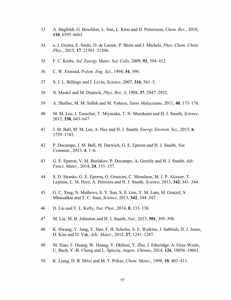
97
33 A. Hagfeldt, G. Boschloo, L. Sun, L. Kloo and H. Pettersson, Chem. Rev., 2010,
110, 6595–6663.
34 a. J. Oostra, E. Smits, D. de Leeuw, P. Blom and J. Michels, Phys. Chem. Chem.
Phys., 2015, 17, 21501–21506.
35 F. C. Krebs, Sol. Energy Mater. Sol. Cells, 2009, 93, 394–412.
36 C. W. Extrand, Polym. Eng. Sci., 1994, 34, 390.
37 S. J. L. Billinge and I. Levin, Science, 2007, 316, 561–5.
38 N. Maskil and M. Deutsch, Phys. Rev. A, 1988, 37, 2947–2952.
39 A. Shafiee, M. M. Salleh and M. Yahaya, Sains Malaysiana, 2011, 40, 173–176.
40 M. M. Lee, J. Teuscher, T. Miyasaka, T. N. Murakami and H. J. Snaith, Science,
2012, 338, 643–647.
41 J. M. Ball, M. M. Lee, A. Hey and H. J. Snaith, Energy Environ. Sci., 2013, 6,
1739–1743.
42 P. Docampo, J. M. Ball, M. Darwich, G. E. Eperon and H. J. Snaith, Nat.
Commun., 2013, 4, 1–6.
43 G. E. Eperon, V. M. Burlakov, P. Docampo, A. Goriely and H. J. Snaith, Adv.
Funct. Mater., 2014, 24, 151–157.
44 S. D. Stranks, G. E. Eperon, G. Grancini, C. Menelaou, M. J. P. Alcocer, T.
Leijtens, L. M. Herz, A. Petrozza and H. J. Snaith, Science, 2013, 342, 341–344.
45 G. C. Xing, N. Mathews, S. Y. Sun, S. S. Lim, Y. M. Lam, M. Gratzel, S.
Mhaisalkar and T. C. Sum, Science, 2013, 342, 344–347.
46 D. Liu and T. L. Kelly, Nat. Phot., 2014, 8, 133–138.
47 M. Liu, M. B. Johnston and H. J. Snaith, Nat., 2013, 501, 395–398.
48 K. Hwang, Y. Jung, Y. Heo, F. H. Scholes, S. E. Watkins, J. Subbiah, D. J. Jones,
D. Kim and D. Vak, Adv. Mater., 2015, 27, 1241–1247.
49 M. Xiao, F. Huang, W. Huang, Y. Dkhissi, Y. Zhu, J. Etheridge, A. Gray-Weale,
U. Bach, Y.-B. Cheng and L. Spiccia, Angew. Chemie, 2014, 126, 10056–10061.
50 K. Liang, D. B. Mitzi and M. T. Prikas, Chem. Mater., 1998, 10, 403–411.
98
51 J. Burschka, N. Pellet, S.-J. Moon, R. Humphry-Baker, P. Gao, M. K. Nazeeruddin
and M. Gratzel, Nat., 2013, 499, 316–319.
52 N. J. Jeon, J. H. Noh, Y. C. Kim, W. S. Yang, S. Ryu and S. Il Seok, Nat. Mater.,
2014, 13, 897–903.
53 Z. Xiao, C. Bi, Y. Shao, Q. Dong, Q. Wang, Y. Yuan, C. Wang, Y. Gao and J.
Huang, Energy Environ. Sci., 2014, 7, 2619–2623.
54 B.-E. Cohen, S. Gamliel and L. Etgar, Apl Mater., 2014, 2, 081502.
55 P. A. Beckmann, Cryst. Res. Technol., 2010, 45, n/a–n/a.
56 J. Yang, B. D. Siempelkamp, D. Liu and T. L. Kelly, ACS Nano, 2015, 9, 1955–63.
57 A. Dualeh, N. Tétreault, T. Moehl, P. Gao, M. K. Nazeeruddin and M. Grätzel,
Adv. Funct. Mater., 2014, 24, 3250–3258.
58 J.-H. Im, I.-H. Jang, N. Pellet, M. Grätzel and N.-G. Park, Nat. Nano., 2014, 9,
927–932.
59 C. Bi, Y. Shao, Y. Yuan, Z. Xiao, C. Wang, Y. Gao and J. Huang, J. Mater. Chem.
A, 2014, 2, 18508–18514.
60 O. Knop, R. E. Wasylishen, M. A. White, T. S. Cameron and M. J. M. Vanoort,
Can. J. Chem. , 1990, 68, 412–422.
61 A. Dualeh, P. Gao, S. Il Seok, M. K. Nazeeruddin and M. Grätzel, Chem. Mater.,
2014, 26, 6160–6164.
62 T. Baikie, Y. Fang, J. M. Kadro, M. Schreyer, F. Wei, S. G. Mhaisalkar, M.
Graetzel and T. J. White, J. Mater. Chem. A, 2013, 1, 5628–5641.
63 N. J. Jeon, H. G. Lee, Y. C. Kim, J. Seo, J. H. Noh, J. Lee and S. Il Seok, J. Am.
Chem. Soc., 2014, 136, 7837–7840.
64 C. He, Q. He, Y. Yi, G. Wu, F. Bai, Z. Shuai and Y. Li, J. Mater. Chem., 2008, 18,
4085.
65 S. Allard, M. Forster, B. Souharce, H. Thiem and U. Scherf, Angew. Chemie - Int.
Ed., 2008, 47, 4070–4098.
66 P. Strohriegl and J. V. Grazulevicius, Adv. Mater., 2002, 14, 1439–1452.
67 Z. Li, T. Ye, S. Tang, C. Wang, D. Ma and Z. Li, J. Mater. Chem. C, 2015, 3,
2016–2023.

99
68 J. J. Wang, S. R. Wang, X. G. Li, L. F. Zhu, Q. B. Meng, Y. Xiao and D. M. Li,
Chem. Commun., 2014, 50, 5829–5832.
69 J. H. Heo, S. H. Im, J. H. Noh, T. N. Mandal, C. S. Lim, J. A. Chang, Y. H. Lee, H.
J. Kim, A. Sarkar, M. K. Nazeeruddin, M. Gratzel and S. I. Seok, Nat. Photonics,
2013, 7, 487–492.
70 H. Choi, S. Park, S. Paek, P. Ekanayake, M. K. Nazeeruddin and J. Ko, J. Mater.
Chem. A, 2014, 2, 19136–19140.
71 S. Do Sung, M. S. Kang, I. T. Choi, H. M. Kim, H. Kim, M. Hong, H. K. Kim and
W. I. Lee, Chem. Commun., 2014, 50, 14161–14163.
72 T. Malinauskas, M. Daskeviciene, G. Bubniene, I. Petrikyte, S. Raisys, K.
Kazlauskas, V. Gaidelis, V. Jankauskas, R. Maldzius, S. Jursenas and V. Getautis,
Chem. Eur. J., 2013, 19, 15044–15056.
73 N. Satoh, T. Nakashima and K. Yamamoto, J. Am. Chem. Soc., 2005, 127, 13030–
13038.
74 D. J. Burke and D. J. Lipomi, Energy Environ. Sci., 2013, 6, 2053–2066.
75 M. N. Belgacem and A. Gandini, Monomers, polymers and composites from
renewable resources, Elsevier, 2011.
76 O. Gidron, A. Dadvand, Y. Sheynin, M. Bendikov and D. F. Perepichka, Chem.
Commun., 2011, 47, 1976–1978.
77 A. D. Hendsbee, J.-P. Sun, T. M. McCormick, I. G. Hill and G. C. Welch, Org.
Electron., 2015, 18, 118–125.
78 K. Oniwa, T. Kanagasekaran, T. Jin, M. Akhtaruzzaman, Y. Yamamoto, H.
Tamura, I. Hamada, H. Shimotani, N. Asao, S. Ikeda and K. Tanigaki, J. Mater.
Chem. C, 2013, 1, 4163–4170.
79 J. Liu, B. Walker, A. Tamayo, Y. Zhang and T.-Q. Nguyen, Adv. Funct. Mater.,
2013, 23, 47–56.
80 A. B. Tamayo, M. Tantiwiwat, B. Walker and T.-Q. Nguyen, J. Phys. Chem. C,
2008, 112, 15543–15552.
81 J. A. Love, C. M. Proctor, J. Liu, C. J. Takacs, A. Sharenko, T. S. van der Poll, A.
J. Heeger, G. C. Bazan and T.-Q. Nguyen, Adv. Funct. Mater., 2013, 23, 5019–
5026.

100
82 T. S. van der Poll, J. A. Love, T.-Q. Nguyen and G. C. Bazan, Adv. Mater., 2012,
24, 3646–3649.
83 Y. Zhao, A. M. Nardes and K. Zhu, Appl. Phys. Lett., 2014, 104, 21306.
84 J. Meyer, S. Hamwi, M. Kröger, W. Kowalsky, T. Riedl and A. Kahn, Adv. Mater.,
2012, 24, 5408–27.
85 A. Abrusci, S. D. Stranks, P. Docampo, H.-L. Yip, A. K. Y. Jen and H. J. Snaith,
Nano Lett., 2013, 13, 3124–3128.
86 M. G. Helander, M. T. Greiner, Z. B. Wang, W. M. Tang and Z. H. Lu, J. Vac. Sci.
& Technol. A, 2011, 29, 011019.
87 G. C. Welch, L. A. Perez, C. V. Hoven, Y. Zhang, X.-D. Dang, A. Sharenko, M. F.
Toney, E. J. Kramer, T.-Q. Nguyen and G. C. Bazan, J. Mater. Chem., 2011, 21,
12700.
88 M. Cheng, C. Chen, X. Yang, J. Huang, F. Zhang, B. Xu and L. Sun, Chem.
Mater., 2015, 27, 1808–1814.
89 L. A. Perez, J. T. Rogers, M. A. Brady, Y. Sun, G. C. Welch, K. Schmidt, M. F.
Toney, H. Jinnai, A. J. Heeger, M. L. Chabinyc, G. C. Bazan and E. J. Kramer,
Chem. Mater., 2014, 26, 6531–6541.
90 R. B. Ross, C. M. Cardona, D. M. Guldi, S. G. Sankaranarayanan, M. O. Reese, N.
Kopidakis, J. Peet, B. Walker, G. C. Bazan, E. Van Keuren, B. C. Holloway and
M. Drees, Nat. Mater., 2009, 8, 208–212.
91 Y. He, H.-Y. Chen, J. Hou and Y. Li, J. Am. Chem. Soc., 2010, 132, 1377–1382.
92 J. Roncali, P. Leriche and A. Cravino, Adv. Mater., 2007, 19, 2045–2060.
93 D. M. Guldi, Chem. Commun., 2000, 321–327.
94 L. A. Perez, K. W. Chou, J. A. Love, T. S. van der Poll, D.-M. Smilgies, T.-Q.
Nguyen, E. J. Kramer, A. Amassian and G. C. Bazan, Adv. Mater., 2013, 25,
6380–6384.
95 J.-Y. Pan, L.-J. Zuo, X.-L. Hu, W.-F. Fu, M.-R. Chen, L. Fu, X. Gu, H.-Q. Shi, M.-
M. Shi, H.-Y. Li and H.-Z. Chen, ACS Appl. Mater. Interfaces, 2013, 5, 972–980.
96 J. Zhang, D. Deng, C. He, Y. He, M. Zhang, Z.-G. Zhang, Z. Zhang and Y. Li,
Chem. Mater., 2011, 23, 817–822.
101
97 J. Zhang, Y. Yang, C. He, D. Deng, Z. Li and Y. Li, J. Phys. D. Appl. Phys., 2011,
44, 475101.
98 H. Shang, H. Fan, Y. Liu, W. Hu, Y. Li and X. Zhan, Adv. Mater., 2011, 23, 1554–
1557.
99 A. D. Hendsbee, J.-P. Sun, L. R. Rutledge, I. G. Hill and G. C. Welch, J. Mater.
Chem. A, 2014, 2, 4198–4207.
100 Y. Kim, A. Ballantyne, J. Nelson and D. Bradley, Org. Electron., 2009, 10, 205–
209.
101 S. Qu and H. Tian, Chem. Commun. (Camb)., 2012, 48, 3039–51.
102 Z. Du, W. Chen, Y. Chen, S. Qiao, X. Bao, S. Wen, M. Sun, L. Han and R. Yang,
J. Mater. Chem. A, 2014, 2, 15904–15911.
103 B. Kan, Q. Zhang, M. Li, X. Wan, W. Ni, G. Long, Y. Wang, X. Yang, H. Feng
and Y. Chen, J. Am. Chem. Soc., 2014, 136, 15529–15532.
104 Z. Yi, W. Ni, Q. Zhang, M. Li, B. Kan, X. Wan and Y. Chen, J. Mater. Chem. C,
2014, 2, 7247–7255.
105 J. W. Ryan and Y. Matsuo, Sci. Rep., 2015, 5.
106 J.-H. Im, C.-R. Lee, J.-W. Lee, S.-W. Park and N.-G. Park, Nanoscale, 2011, 3,
4088–4093.
107 H. Li, K. Fu, A. Hagfeldt, M. Grätzel, S. G. Mhaisalkar and A. C. Grimsdale,
Angew. Chemie - Int. Ed., 2014, 53, 4085–4088.
108 S. Sun, T. Salim, N. Mathews, M. Duchamp, C. Boothroyd, G. Xing, T. C. Sum
and Y. M. Lam, Energy Environ. Sci., 2014, 7, 399–407.
109 H. Li, K. Fu, P. P. Boix, L. H. Wong, A. Hagfeldt, M. Grätzel, S. G. Mhaisalkar
and A. C. Grimsdale, ChemSusChem, 2014, 7, 3420–3425.
110 L. Zheng, Y. S. Chung, Y. Ma, L. Zhang, L. Xiao, Z. Chen, S. Wang, B. Qu and Q.
Gong, Chem. Commun., 2014, 1, 1–4.
111 D. Bi, L. Yang, G. Boschloo, A. Hagfeldt and E. M. J. Johansson, J. Phys. Chem.
Lett., 2013, 4, 1532–1536.
112 F. Matteocci, S. Razza, F. Di Giacomo, S. Casaluci, G. Mincuzzi, T. M. Brown, A.
D’Epifanio, S. Licoccia and A. Di Carlo, Phys. Chem. Chem. Phys., 2014, 16,
3918–3923.
102
113 Y. S. Kwon, J. Lim, H.-J. Yun, Y.-H. Kim and T. Park, Energy Environ. Sci.,
2014, 7, 1454–1460.
114 H. J. Snaith and M. Gratzel, Appl. Phys. Lett., 2006, 89, 262113–262114.
115 A. Abate, T. Leijtens, S. Pathak, J. Teuscher, R. Avolio, M. E. Errico, J.
Kirkpatrik, J. M. Ball, P. Docampo, I. McPherson and H. J. Snaith, Phys. Chem.
Chem. Phys., 2013, 15, 2572–2579.
116 W. H. Howie, J. E. Harris, J. R. Jennings and L. M. Peter, Sol. Energy Mater. Sol.
Cells, 2007, 91, 424–426.
117 Y. Huang, W. Wen, S. Mukherjee, H. Ade, E. J. Kramer and G. C. Bazan, Adv.
Mater., 2014, 26, 4168–4172.
118 H. Li, T. Earmme, G. Ren, A. Saeki, S. Yoshikawa, N. M. Murari, S.
Subramaniyan, M. J. Crane, S. Seki and S. A. Jenekhe, J. Am. Chem. Soc., 2014,
136, 14589–14597.
119 W. Jiang, L. Ye, X. Li, C. Xiao, F. Tan, W. Zhao, J. Hou and Z. Wang, Chem.
Commun., 2014, 50, 1024–1026.
120 Y. Zang, C.-Z. Li, C.-C. Chueh, S. T. Williams, W. Jiang, Z.-H. Wang, J.-S. Yu
and A. K.-Y. Jen, Adv. Mater., 2014, 26, 5708–14.
121 J. Zhao, Y. Li, H. Lin, Y. Liu, K. Jiang, C. Mu, T. Ma, J. Y. Lin Lai, H. Hu, D. Yu
and H. Yan, Energy Environ. Sci., 2015, 8, 520–525.
122 W. Chen, X. Yang, G. Long, X. Wan, Y. Chen and Q. Zhang, J. Mater. Chem. C,
2015, 3, 4698–4705.
123 S.-Y. Liu, C.-H. Wu, C.-Z. Li, S.-Q. Liu, K.-H. Wei, H.-Z. Chen and A. K.-Y. Jen,
Adv. Sci., 2015, 2, 1500014.
124 Y. Liu, C. Mu, K. Jiang, J. Zhao, Y. Li, L. Zhang, Z. Li, J. Y. L. Lai, H. Hu, T. Ma,
R. Hu, D. Yu, X. Huang, B. Z. Tang and H. Yan, Adv. Mater., 2015, 27, 1014–
1014.
125 Y. Lin, P. Cheng, Y. Li and X. Zhan, Chem. Commun., 2012, 48, 4773–4775.
126 Y. Lin, Y. Wang, J. Wang, J. Hou, Y. Li, D. Zhu and X. Zhan, Adv. Mater., 2014,
26, 5137–5142.
127 A. Sharenko, D. Gehrig, F. Laquai and T.-Q. Nguyen, Chem. Mater., 2014, 26,
4109–4118.

103
128 A. Sharenko, C. M. Proctor, T. S. van der Poll, Z. B. Henson, T.-Q. Nguyen and G.
C. Bazan, Adv. Mater., 2013, 25, 4403–6.
129 R. Singh, E. Aluicio-Sarduy, Z. Kan, T. Ye, R. C. I. MacKenzie and P. E.
Keivanidis, J. Mater. Chem. A, 2014, 2, 14348–14353.
130 M. Li, J. Liu, X. Cao, K. Zhou, Q. Zhao, X. Yu, R. Xing and Y. Han, Phys. Chem.
Chem. Phys., 2014, 16, 26917–26928.
104
APPENDIX A – SOLUTION PREPARATIONS
TiO2 Precursor Solution Preparation
To form the compact TiO2 layer, a precursor solution containing titanium (IV)
isopropoxide (Ti(iPrO)4), purchased from Sigma-Aldrich, Product No. 377996-25ML,
99.999% purity) was prepared using a modified procedure outlined by Abrusci et al.85 Two
solutions were prepared in separate 8 mL vials. The first vial contained 2530 μL of ethanol
and 35 μL of a stock solution of 2.0 M HCl (prepared in air). The second solution contained
2530 μL of ethanol and 370 μL of Ti(iPrO)4 (prepared in the glovebox). The first solution
was added dropwise to the second solution while the second was stirred in air to form the
final sol-gel solution.
PbI2 Solution Preparation
A 1.0 M PbI2 solution was prepared by weighing 461 mg of PbI2 (purchased from
Alfa-Aesar, Product No. 12724, 99.9985% purity) in a 4- or 8-mL Teflon-capped vial and
adding 1000 μL of dry DMF and a stir bar. The solid was dissolved by heating and stirring
on a hotplate and maintained at the desired temperature throughout the deposition
procedure. The temperature of the solution was recorded by attaching a thermocouple
probe to the outer wall of the vial. The 0.5 M and 0.75 M PbI2 solutions were prepared in
a similar fashion, but dissolved by stirring at RT.
Spiro-OMeTAD (Doped) Solution Preparation
The HTM solution was prepared using the recipe described by Liu et al.46: 80 mg
of spiro-OMeTAD (purchased from Sigma-Aldrich, Product No. 792071-1G, 99% purity),
28.5 µL of 4-tert-butylpyridine (tBP, purchased from Sigma-Aldrich, Product No. 142379-
25G, 96% purity) and 17.5 µL of a 520 mg/mL solution of lithium-
bis(trifluoromethane)sulfonimide (Li-TFSI, purchased from Sigma-Aldrich, Product No.

105
544094-5G, 99.95% purity) in acetonitrile was combined and dissolved 1 mL of
chlorobenzene. The solid spiro-OMeTAD was weighed onto a weigh paper and then
transferred to a 4.0 mL Teflon®-capped vial. tBP, chlorobenzene and the Li-TFSI solution
were transferred separately into the vial using micropipettes. The mixture was dissolved
using a stir-bar and stirring at RT.

106
APPENDIX B – SYNTHESIS OF CH3NH3I
The synthesis of CH3NH3I was performed using the procedure documented by Im
et al. as a guideline.106 A 250 mL round-bottom flask was loaded with 27 mL of 55 wt-%
HI(aq) (BC Scientific, Product No. 0152-01), 30 mL of a 40% aqueous solution of
methylamine (Fisher Scientific, Product No. 00983) and a stir bar. The reaction mixture
was stirred in an ice bath in air for 3 h. The solvent was removed using a rotary evaporator,
leaving behind a brown solid. The solid product was slurried in diethyl ether for 30 minutes
and filtered using a Buchner funnel. This process was repeated twice more to wash the
product. The washed final product was recrystallized from a minimum amount of ethanol,
cooled, and filtered to recover white crystals. The crystals were washed with diethyl ether
and dried in a vacuum oven overnight. The solid crystalline product was stored in an Ar-
filled glovebox prior to use.

107
APPENDIX C – OTHER FACTORS INFLUENCING LEAD IODIDE FILM
MORPHOLOGY
Solution Temperature (Tsolution)
It was determined that the minimum value of Tsolution for complete dissolution of a
1.0 M solution of PbI2 in DMF was 50 °C. Increasing Tsolution above the threshold
temperature (i.e., 50 °C) results in perovskite films with smaller crystallites (Figure C1).
However, there are no significant differences between the films cast from solutions held at
70, 90, 110, and 130 °C in terms of crystallite size and distribution.
Figure C1. The effect of solution temperature. SEM images of PbI2 films spin-cast on
TiO2 compact films at different temperatures and the corresponding CH3NH3PbI3 films
after conversion via dipping. The solution was spin-coated using a spin speed of 3000 rpm
for 30 s onto TiO2-coated substrates heated at 100 °C.
The Effect of Atmosphere
By depositing onto a hot substrate or performing the deposition under an inert (i.e.,
Ar) atmosphere, film coverage can be drastically improved. In both cases, the films exhibit
smaller grain sizes and better coverage than the unheated film in ambient. It is also
observed that the film spun under ambient conditions with a heated substrate had a lower
frequency of pinholes than the one spun in the glovebox (see Figure C2). This
demonstrates that inert conditions are not required for uniform film formation – simply

108
heating the substrate prior to deposition is an effective method for hindering crystal growth
and increasing film coverage.
Figure C2. The effect of atmosphere on PbI2 film formation. Depicted are SEM images
of PbI2 and corresponding CH3NH3PbI3 films spin-cast from a 1.0 M PbI2 solution in DMF
held at 70 °C. The solution was spin-coated in either air (ambient) or N2 (inert) using a
spin speed of 1000 rpm for 30 s onto substrates held at either R.T. or 100 °C.

109
APPENDIX D – PEROVSKITE X-RAY DIFFRACTION PEAK
INTENSITIES
Table D1. Peak areas corresponding to XRD plots in Figure 3.15, determined by
applying the Pearson VII function and using Jade software.
[MAI] Peak
Area for
PbI2
(001)
PbI2
(001)
Error
Peak
Area for
MAPbI3
(110)
MAPbI3
(110)
Error
IPbI2/(IPbI2 +
IMAPbI3)
IPbI2/(IPbI2 +
IMAPbI3)
Error
20 5662.7 37.8 2319.9 26.7 0.70938 0.010559
30 3760.1 32.3 2636.1 26.4 0.587865 0.009255
40 1933.3 25.6 3833.2 31.1 0.335264 0.006842
50 71.4 12.5 4592.7 N/A 0.015308 0.00379
For simplicity, let:
IPbI2/(IPbI2 + IMAPbI3) = A
Error for IPbI2/(IPbI2 + IMAPbI3) = δA
IPbI2 = B
Error for IPbI2 = δB
IMAPbI3 = C
Error for C = δC
Calculation of error:
δA = |A| (2*( δB/B)2 + (δC/C)2)1/2

110
APPENDIX E – THIOPHENE IN ORGANIC SMALL MOLECULES
Thiophene heterocyclic derivatives are important electron-donating (D)
functionalities in organic HTMs. There are a number of reports of high-performance small-
molecule HTMs designed for applications in PSCs based on thiophene derivatives – the
molecular structure of three examples are given in Figure E1. In the first example, a simple
HTM known as “H101” was synthesized and shown to achieve a respectable PCE of 10.6
% without the use of dopants. In this molecule, 3,4-ethylenedioxythiophene (EDOT)
core107 was used in an shown to produce higher currents than unsubstituted benzene or
thiophene. EDOT is a common functional group in HTMs, with a popular example being
the mixture of poly(3,4-ethylenedioxythiophene) polystyrene sulfonate (PEDOT:PSS).
Although mostly used for OPVs, PEDOT:PSS is now gaining attention as the HTL in
inverted PSCs.23,24,108 In a subsequent paper, the same group reported a derivative of H101
with a tetra-substituted thiophene core (aka “H111”) that achieved a PCE of 14.9 %;109 to
date, it is the highest reported PCE for PSCs without Spiro-OMeTAD. A third example is
a thiophene oligomer with benzodithiophene (BDT) core, named “DR3TBDTT”.110 From
DFT studies the HOMO is located at BDT unit, and the LUMO occupies the electron-
drawing ethylrhodanine groups at both ends, suggesting that that hole-transport may be
occurring primarily at the core in this acceptor–donor–acceptor backbone electronic
structure. Three thiophene bridging units extend conjugation from the core to the ends.
Unlike the previous two examples, devices with DR3TBDTT performed worse when doped
with Li-TFSI and tBP, suggesting that structural differences are a factor in the response to
such dopants.
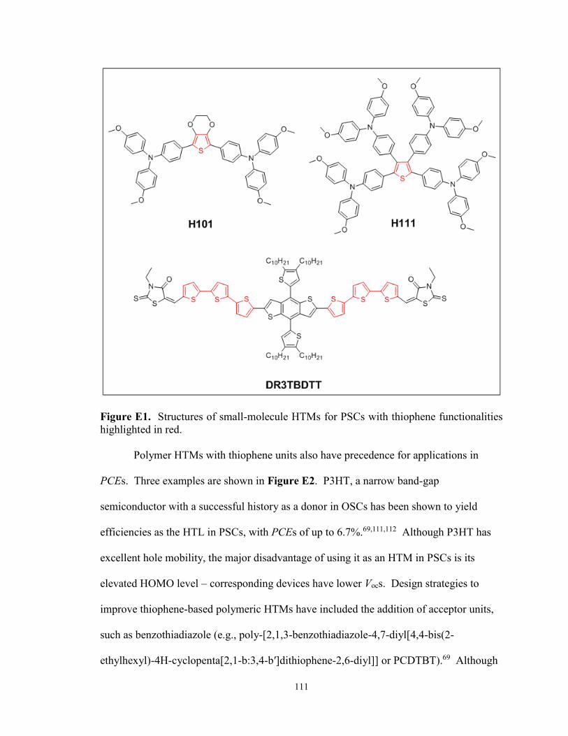
111
Figure E1. Structures of small-molecule HTMs for PSCs with thiophene functionalities
highlighted in red.
Polymer HTMs with thiophene units also have precedence for applications in
PCEs. Three examples are shown in Figure E2. P3HT, a narrow band-gap
semiconductor with a successful history as a donor in OSCs has been shown to yield
efficiencies as the HTL in PSCs, with PCEs of up to 6.7%.69,111,112 Although P3HT has
excellent hole mobility, the major disadvantage of using it as an HTM in PSCs is its
elevated HOMO level – corresponding devices have lower Vocs. Design strategies to
improve thiophene-based polymeric HTMs have included the addition of acceptor units,
such as benzothiadiazole (e.g., poly-[2,1,3-benzothiadiazole-4,7-diyl[4,4-bis(2-
ethylhexyl)-4H-cyclopenta[2,1-b:3,4-b′]dithiophene-2,6-diyl]] or PCDTBT).69 Although
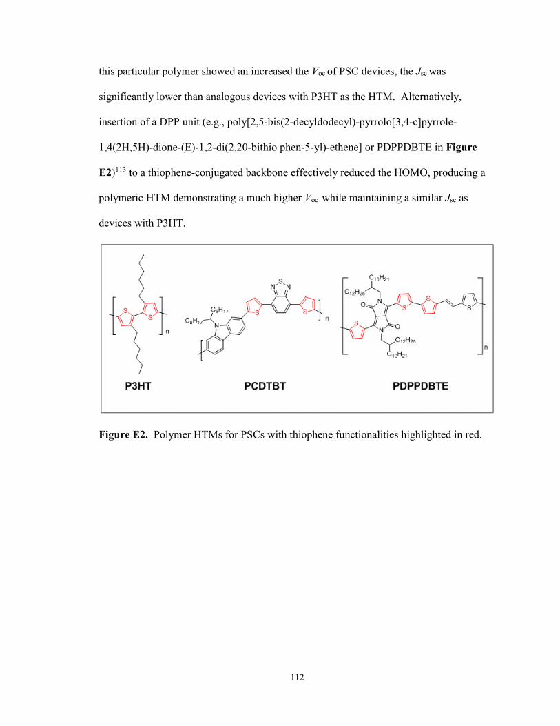
112
this particular polymer showed an increased the Voc of PSC devices, the Jsc was
significantly lower than analogous devices with P3HT as the HTM. Alternatively,
insertion of a DPP unit (e.g., poly[2,5-bis(2-decyldodecyl)-pyrrolo[3,4-c]pyrrole-
1,4(2H,5H)-dione-(E)-1,2-di(2,20-bithio phen-5-yl)-ethene] or PDPPDBTE in Figure
E2)113 to a thiophene-conjugated backbone effectively reduced the HOMO, producing a
polymeric HTM demonstrating a much higher Voc while maintaining a similar Jsc as
devices with P3HT.
Figure E2. Polymer HTMs for PSCs with thiophene functionalities highlighted in red.
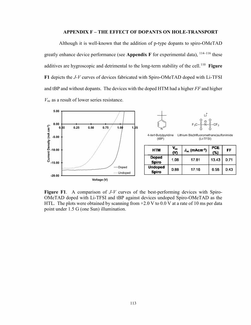
113
APPENDIX F – THE EFFECT OF DOPANTS ON HOLE-TRANSPORT
Although it is well-known that the addition of p-type dopants to spiro-OMeTAD
greatly enhance device performance (see Appendix F for experimental data), 114–116 these
additives are hygroscopic and detrimental to the long-term stability of the cell.110 Figure
F1 depicts the J-V curves of devices fabricated with Spiro-OMeTAD doped with Li-TFSI
and tBP and without dopants. The devices with the doped HTM had a higher FF and higher
Voc as a result of lower series resistance.
Figure F1. A comparison of J-V curves of the best-performing devices with Spiro-
OMeTAD doped with Li-TFSI and tBP against devices undoped Spiro-OMeTAD as the
HTL. The plots were obtained by scanning from +2.0 V to 0.0 V at a rate of 10 ms per data
point under 1.5 G (one Sun) illumination.
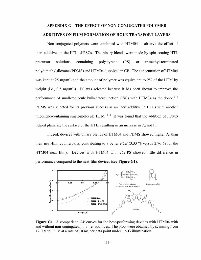
114
APPENDIX G – THE EFFECT OF NON-CONJUGATED POLYMER
ADDITIVES ON FILM FORMATION OF HOLE-TRANSPORT LAYERS
Non-conjugated polymers were combined with HTM04 to observe the effect of
inert additives in the HTL of PSCs. The binary blends were made by spin-coating HTL
precursor solutions containing polystyrene (PS) or trimethyl-terminated
polydimethylsiloxane (PDMS) and HTM04 dissolved in CB. The concentration of HTM04
was kept at 25 mg/mL and the amount of polymer was equivalent to 2% of the HTM by
weight (i.e., 0.5 mg/mL). PS was selected because it has been shown to improve the
performance of small-molecule bulk-heterojunction OSCs with HTM04 as the donor.117
PDMS was selected for its previous success as an inert additive in HTLs with another
thiophene-containing small-molecule HTM. 110 It was found that the addition of PDMS
helped planarize the surface of the HTL, resulting in an increase in Jsc and FF.
Indeed, devices with binary blends of HTM04 and PDMS showed higher Jsc than
their neat-film counterparts, contributing to a better PCE (3.33 % versus 2.76 % for the
HTM04 neat film). Devices with HTM04 with 2% PS showed little difference in
performance compared to the neat-film devices (see Figure G1).
Figure G1. A comparison J-V curves for the best-performing devices with HTM04 with
and without non-conjugated polymer additives. The plots were obtained by scanning from
+2.0 V to 0.0 V at a rate of 10 ms per data point under 1.5 G illumination.

115
Table G1. Summary of J-V characteristics of devices with HTM04 as the HTM with and
without non-conjugated polymer additives. All measurements were taken by scanning
from +2.0 V to 0.0 V with a scan delay of 10 ms under 1.5 G illumination.
HTL Voc (V) Jsc (mA
cm-2)
PCE
(%) FF
Shunt
Resistance
(Ω/cm2)
Series
Resistance
(Ω/cm2)
HTM04 neat 0.89 10.02 2.76 0.31 1.74×10⁵ 7.46×10⁻²
HTM04 + 2% PS 0.87 9.35 2.71 0.33 2.13×10⁵ 7.34×10⁻²
HTM04 + 2% PDMS 0.85 11.87 3.33 0.33 2.20×10⁵ 7.58×10⁻²
AFM images of the HTL surfaces reveal that films with HTM04 and PDMS on a
perovskite active layer are less rough than HTM04 neat films on perovskite (see Figure
G2). The images suggest that the addition of PDMS planarizes the HTL by filling in the
deep “valleys” in the perovskite film. On the other hand, the roughness of the films with
and without PS are very similar. Interestingly, addition of either polymer improved the
shunt resistance of the devices, which gives further evidence that the blends are providing
better coverage of the perovskite layer, and thus passivating shunt pathways.
Figure G2. 2D AFM images of HTL surfaces of HTM04 with and without polymer
additives on a perovskite film. An image of a neat perovskite film is shown for comparison.
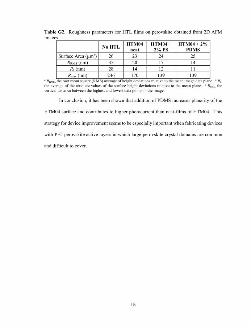
116
Table G2. Roughness parameters for HTL films on perovskite obtained from 2D AFM
images.
No HTL HTM04
neat
HTM04 +
2% PS
HTM04 + 2%
PDMS
Surface Area (µm²) 26 23 24 25
RRMS (nm) 35 20 17 14
Ra (nm) 28 14 12 11
Rmax (nm) 246 170 139 139 a RRMS, the root mean square (RMS) average of height deviations relative to the mean image data plane. b Ra,
the average of the absolute values of the surface height deviations relative to the mean plane. c Rmax, the
vertical distance between the highest and lowest data points in the image.
In conclusion, it has been shown that addition of PDMS increases planarity of the
HTM04 surface and contributes to higher photocurrent than neat-films of HTM04. This
strategy for device improvement seems to be especially important when fabricating devices
with PHJ perovskite active layers in which large perovskite crystal domains are common
and difficult to cover.
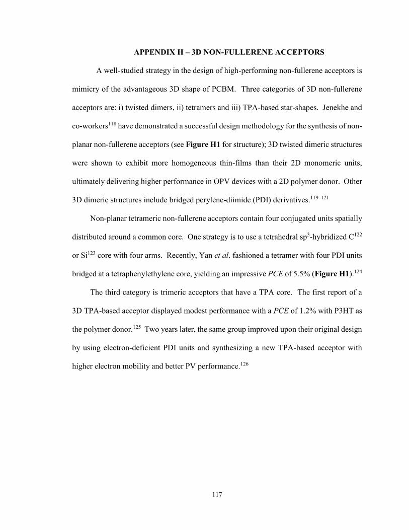
117
APPENDIX H – 3D NON-FULLERENE ACCEPTORS
A well-studied strategy in the design of high-performing non-fullerene acceptors is
mimicry of the advantageous 3D shape of PCBM. Three categories of 3D non-fullerene
acceptors are: i) twisted dimers, ii) tetramers and iii) TPA-based star-shapes. Jenekhe and
co-workers118 have demonstrated a successful design methodology for the synthesis of non-
planar non-fullerene acceptors (see Figure H1 for structure); 3D twisted dimeric structures
were shown to exhibit more homogeneous thin-films than their 2D monomeric units,
ultimately delivering higher performance in OPV devices with a 2D polymer donor. Other
3D dimeric structures include bridged perylene-diimide (PDI) derivatives.119–121
Non-planar tetrameric non-fullerene acceptors contain four conjugated units spatially
distributed around a common core. One strategy is to use a tetrahedral sp3-hybridized C122
or Si123 core with four arms. Recently, Yan et al. fashioned a tetramer with four PDI units
bridged at a tetraphenylethylene core, yielding an impressive PCE of 5.5% (Figure H1).124
The third category is trimeric acceptors that have a TPA core. The first report of a
3D TPA-based acceptor displayed modest performance with a PCE of 1.2% with P3HT as
the polymer donor.125 Two years later, the same group improved upon their original design
by using electron-deficient PDI units and synthesizing a new TPA-based acceptor with
higher electron mobility and better PV performance.126
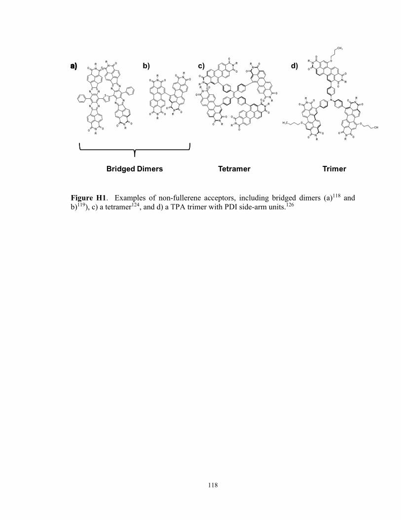
118
Figure H1. Examples of non-fullerene acceptors, including bridged dimers (a)118 and
b)119), c) a tetramer124, and d) a TPA trimer with PDI side-arm units.126

119
APPENDIX I – VARYING DONOR-ACCEPTOR RATIOS
Figure I1 depicts UV-Vis spectra of D1-A1 and D2-D1 blends spin-cast from
solutions with varying D:A weight ratios. It was confirmed that by reducing the D:A weight
ratio, the relative absorption intensity of A1 increases, balancing the absorption of the film
across the spectrum. However, if the concentration of the precursor solution is fixed at 30
mg/mL, while reducing the D:A ratio, the total absorbance of the film is reduced. Since
there is a trade-off between absorption balance and total absorbance, only fabrication of
devices with the different ratios can determine the optimal ratio for OPVs.
Figure I1. UV-Vis absorption spectra acquired for as-cast blend films of a) D1-A1 and b)
D2-A1 with varying D:A weight ratios. Spectra were acquired by Arthur Hendsbee.

120
Figure I2. XRD patterns of thin-film blends with D1-A1 ratios of a) 1:1 and b) 1:2 acquired
before and after thermal annealing for 120 min at 150 °C. The A1 diffraction peak is higher
in relative intensity in the pattern for the 1:2 film than in the 1:1 due to the higher quantity
of crystalline material.

121
APPENDIX J – SOLVENT ADDITIVES AND SOLVENT VAPOUR ANNEALING
In Chapter 4, thermal annealing was used as a processing technique to modify the
structure and morphology of thin film blends of D1-A1. Two other techniques that can be
applied to formation of thin films and the fabrication of OSCs are the use of solvent
additives and solvent vapour annealing.
Solvent Additives
Solvent additives are typically high-boiling liquids that are co-dissolved with the
photoactive materials in the spin-coating solution. The most common solvent additive is
1,8-diiodooctane (DIO), which has been shown to yield remarkable improvements in a
variety of OPV systems.127–129 Nevertheless, other solvent additives have also been
shown to induce different and favourable changes in thin film OSCs.130
In a preliminary study, three different high-boiling compounds were selected as
solvent additives for the D1-A1 systems. In separate samples, either DIO, 4-
trifluoromethyl benzoic acid (4-TFBA) or 1-naphthaldehyde (1-NA) were used as solvent
additives in the solutions containing D1 and A1 in a 1:1 weight ratio with a total solid
concentration of 20 mg/mL. A stock solution of each solvent additive was first prepared
in CHCl3 at a concentration of 4% (v/v%). D1-A1 solutions were prepared by combining
the weighed solid compounds with a measured mixture of the solvent-additive stock
solution and pure CHCl3 as per the volumes listed in Table J1. All volumes of solvent and
solvent additive were measured with either a 200-μL or 1000-μL micropipette.
Table J1. Compositions of solvents with solvent-additive.
Volume %
Additive
Total Solution
Volume (μL)
Volume of
Additive (μL)
Volume of
Stock Solution
(μL)
Volume of
Pure CHCl3
(μL)
0.4 1000 4 100 900
1.0 1000 10 250 750

122
From the UV-Vis spectra depicted in Figure J1, it is observed that small
quantities of each of the solvent additives have negligible effects on the absorption
properties of D1 and A1. However, increasing the concentration of the DIO (Figure J1
a)) and 1-NA (Figure J1 c)) to 1.0% results in changes to the absorption profile of A1
and emergence of three distinct bands and a reduction in the intensity of the high-energy
absorption band of D1. On the other hand, addition of 1.0% of 1-TFBA results in a
broadening of the A1 absorption, but no significant changes in the absorption of D1.
Although it is clear that electronic changes occur within the films from the presence of
the solvent additives, structural changes could not be detected using XRD (Figure J1 d),
e), f)). In this case, AFM is an ideal tool to probe the films for morphological changes.
However, these experiments have yet to be performed.
Figure J1. UV-Vis spectra of D1-A1 blend thin films (1:1 weight ratio) with various
amounts of solvent additives: a) DIO, b) 4-TFBA and c) 1-NA. Also shown are XRD
patterns of the blend films with d) DIO, e) 4-TFBA and f) 1-NA.
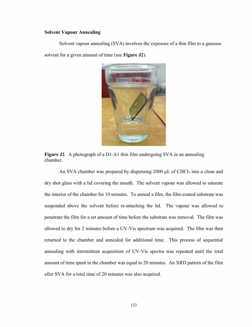
123
Solvent Vapour Annealing
Solvent vapour annealing (SVA) involves the exposure of a thin film to a gaseous
solvent for a given amount of time (see Figure J2).
Figure J2. A photograph of a D1-A1 thin film undergoing SVA in an annealing
chamber.
An SVA chamber was prepared by dispensing 2000 μL of CHCl3 into a clean and
dry shot glass with a lid covering the mouth. The solvent vapour was allowed to saturate
the interior of the chamber for 10 minutes. To anneal a film, the film-coated substrate was
suspended above the solvent before re-attaching the lid. The vapour was allowed to
penetrate the film for a set amount of time before the substrate was removal. The film was
allowed to dry for 2 minutes before a UV-Vis spectrum was acquired. The film was then
returned to the chamber and annealed for additional time. This process of sequential
annealing with intermittent acquisition of UV-Vis spectra was repeated until the total
amount of time spent in the chamber was equal to 20 minutes. An XRD pattern of the film
after SVA for a total time of 20 minutes was also acquired.
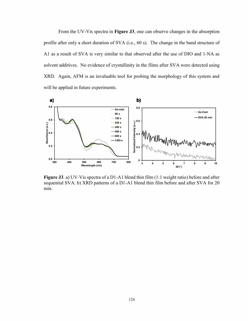
124
From the UV-Vis spectra in Figure J3, one can observe changes in the absorption
profile after only a short duration of SVA (i.e., 60 s). The change in the band structure of
A1 as a result of SVA is very similar to that observed after the use of DIO and 1-NA as
solvent additives. No evidence of crystallinity in the films after SVA were detected using
XRD. Again, AFM is an invaluable tool for probing the morphology of this system and
will be applied in future experiments.
Figure J3. a) UV-Vis spectra of a D1-A1 blend thin film (1:1 weight ratio) before and after
sequential SVA. b) XRD patterns of a D1-A1 blend thin film before and after SVA for 20
min.