Embed Size (px)
Citation preview

Fabrication of solution-processed photoactive polymer- and halide perovskite-based solar cells
RAHAQ, Yaqub Shayi
Available from Sheffield Hallam University Research Archive (SHURA) at:
http://shura.shu.ac.uk/16822/
This document is the author deposited version. You are advised to consult the publisher's version if you wish to cite from it.
Published version
RAHAQ, Yaqub Shayi (2017). Fabrication of solution-processed photoactive polymer- and halide perovskite-based solar cells. Doctoral, Sheffield Hallam University.
Copyright and re-use policy
See http://shura.shu.ac.uk/information.html
Sheffield Hallam University Research Archivehttp://shura.shu.ac.uk

Fabrication of Solution-processed Photoactive
Polymer- and Halide Perovskite-based Solar Cells
Yaqub Shayi Rahaq
A thesis submitted in partial fulfilment of the requirements of
Sheffield Hallam University
for the degree of Doctor of Philosophy
2017

i
Declaration
I hereby declare that this thesis submitted for the degree of PhD is the result of my own
research and that this thesis has not been submitted for higher degree to any other
university or institution.
Yaqub Shayi Rahaq

ii
Dedication
To my father and my mother, your sacrifices won't be forgotten
To my beloved wife (Kalthom), and my children (Jumana, Yousef, Abdulrahman, Zain
and Omar)
This effort is a small gift to all of you
Yaqub Shayi Rahaq

iii
Acknowledgement
First and foremost, I would like to express my sincere gratitude to my supervisor Dr.
Heming Wang for his valuable guidance, continued support and enlightenment during
the journey of my PhD.
I would appreciate his great attention that he paid to my research throughout the past
four years as I gained encouragement and support to complete the work. I would also
like to thank my second supervisor, Dr Aseel Hassan for his support, assistance and
consideration on revising my thesis. Also, I would thank all the member of staff for
their support; Prof. Alan Smith, Prof. Doug Cleaver, Dr. Nicholas Farmilo, Dr. Hywel
Jones, Dr. Danial Loch, Dr. Francis Clegg, Dr. Fares alnaemi, Dr Akram Khan and Dr.
Abbas Hashim.
I would thank my PhD colleagues and friends who have helped me in the labs: Dr.
Vikas Kumar, Dr. Burak Khadem, Abubaker, Magdi, Ronak, Dr. Nayef Alenezi, Faraj,
Abdusalam, Olly, Kalid Shahriar, Salim, Eman, Amani, Mirjam, Hisham, Olu, Madugu,
Mohammed, Abdullah, Ali, Hadi, Ojo, Ibrahim, Dignesh and. Mathew.
Deep gratitude to all MERI staff and technicians who were constantly of assistance.
Finally, heartfelt thanks to my Father, Mother, Wife, children and my siblings, for their
support, guidance, patience and encouragement.

iv
Abstract
In the current work, different architectures and photoactive materials have been
investigated in order to fabricate low-temperature solution-processed solar cells using
dip and spin coating methods.
Inverted bulk heterojunction structure has been utilised in fabrication of polymer solar
cells using dip coating method. In this structure, all layers except electrodes were
deposited using dip coating method, which demonstrated an excellent potential to
produce large-scale area PV devices. Formulation of solutions (using different solvents)
of hole transport layer, active layer, and electron transport layer play a key role in
producing uniform thin films as well as compatibility with dip coating method. The best
PV device achieved ~ 3.4% power conversion efficiency.
On the other hand, planar heterojunction structures have been employed to produce
perovskite-based solar cells using one and two step spin coating methods (OSSCM &
TSSCM). Thorough investigations of controlling the morphology of the perovskite
films have been carried out using low-temperature processing methods. It was found
that it is difficult to control the morphology via OSSCM without additives or using
solvent engineering. Controlling the morphology of the perovskite films was achieved
via TSSCM after optimizing process parameters such as the concentration of
methylammonium iodide (MAI), allowed reaction time (Art), and thermal annealing.
In this work it has been established that the best morphology of the perovskite film
was achieved when the 1.0 wt% MAI solution was loaded at 60 sec on top of the pre-
coated PbI2 followed by thermal annealing for two hours.

v
Furthermore, a novel route for fabrication of solar radiation absorbers has been
developed by blending a photoactive conjugated polymer with an organolead halide
perovskite to create a composite photoactive layer for solar light harvesting. The
photoactive polymer did not only contribute to generation of charges, but also enhanced
stability of solar cells by providing a barrier protection to halide perovskites.
vi
List of Abbreviation
AFM atomic force microscopy
Art allowed reaction time
AM air mass
BHJ bulk heterojunction
BCP Bathocuproine
CB conduction band
CIGS Copper indium gallium diselenide
CB Chlorobenzene
DI deionised (water)
DSSC dye sensitized solar cell
DMF Dimethylformamide
DCB Dichlorobenzene
DIO 1,8-diiodooctane
EQE external quantum efficiency
EA electron affinity (χs)
Eb exciton binding energy
ETL electron transporting layer
FF fill factor
HTL hole transport layer
HOMO highest occupied molecular orbital
ITO Indium tin oxide

vii
IP ionisation potential
IR infrared light
ICL interconnecting layers
IPA Isopropanol
Jsc short circuit current
J-V current density-voltage (characteristics)
KB Boltzmann’s constant
k extinction coefficient
LUMO lowest unoccupied molecular orbital
LD exciton diffusion length
MAI Methylammonium iodide
Ms mesoporous
NREL National Renewable Energy Laboratory
OPV organic photovoltaic
OSSCM one-step spin coating method
P3HT poly(3-hexylthiophene-2,5-diyl)
PCE power conversion efficiency
PEDOT: PSS poly(3,4-ethylenedioxythiophene)-poly(styrenesulfonate)
PL photoluminescence
PCBM [6,6]-phenyl-C61-butyric acid methyl ester
PHJ planar heterojunction
PbI2 Lead iodide
PSC polymer solar cells

viii
PTB7 poly[[4,8-bis[(2-ethylhexyl)oxy]benzo[1,2-b:4,5-b′ ]dithiophene-
2,6-diyl][3-fluoro-2-[(2-ethylhexyl)carbonyl] thieno[3,4-b]thiophenediy
rpm revolutions per minute
SEM scanning electron microscopy
SPPDs solution-processable photovoltaic devices
P Max Maximal power output
Spiro-MeOtad 2,2’,7,7’-tetrakis-(N,N-di-p-methoxyphenylamine)λ,λ’-spirobifluorene
TF tolerance factor
TSSCM two-step spin coating method
UV-Vis ultraviolet-visible
VB valance band
XRD X-ray diffraction
VASP vapor-assisted solution process
Voc open circuit voltage
wavelength

ix
List of Publication
Publications
Rahaq, Y., Wang, H., & Kumar, V. (2014). Fabricating the solution-
processable inverted photovoltaic devices by the dip-coating method.
Organic Electronics, 15(5), 984-990.
Wang, H., Rahaq, Y., & Kumar, V. (2016). A composite light-harvesting
layer from photoactive polymer and halide perovskite for planar
heterojunction solar cells. Scientific Reports, 6, 29567.
Patent
I have patent pending: UK Patent application No. 1600577.9. Photovoltaics
polymer-perovskite Composite Materiale, 2016
Conference presentations
Blending photoactive polymer with halide perovskite as light harvesting
layer for solar cells to enhance stability of devices. Valencia, Spain March
2017. The International Conference on Perovskite Thin Film Photovoltaics
(ABXPV17) (oral presentation)
A highly efficient planar hetrojunction solar cells based on hybrid halide
perovskite fabricated via sequential method. London South bank University.
The UK, July 2016. Photovoltaics (PV): strategic alternative energy source
for Egypt; from cell to grid connected PV arrays )oral presentation)

x
Investigation of morphologies and crystallisation of the organometallic
halide perovskites for photovoltaic devices. UK Semiconductor 2015.
Sheffield July 2015. (Poster presentation).
Utilizing Dip Coating method to fabricate the solution processable inverted
photovoltaic devices. Sheffield Hallam University Symposium March 2014.
(oral presentation).
Promotion of crystallisation for the organometal halide perovskite via a
chemical catalyst at low temperature. HOPV2015, Rome Italy, May 2015.
International Conference on Hybrid and Organic Photovoltaics 2015
(HOPV15) (poster presentation).
Enhancement of the processing stability in fabricating organolead halide
perovskite solar cells by a modified two-step method and improvement of
the device stability by introducing a stable sol-gel/ PEDOT:PSS layer.
HOPV2016, Swansea University, July 2016. International Conference on
Hybrid and Organic Photovoltaics (HOPV16) (poster presentation).
Novel Composite Photoactive Layers for Light-Harvesting in Hybrid
Organic-Inorganic Solar Cells. Sheffield Hallam Symposium, December
2016. (poster presentation) (awarded 2nd prize among 110 posters).

xi
Table of Contents
Declaration ............................................................................................................................. i
Dedication .............................................................................................................................. ii
Acknowledgement ................................................................................................................ iii
Abstract ................................................................................................................................ iv
List of Abbreviation ............................................................................................................. vi
List of Publication ................................................................................................................ ix
Table of Contents ................................................................................................................. xi
List of Figures .................................................................................................................... xvi
List of Tables ...................................................................................................................... xxi
Introduction .......................................................................................................1 Chapter 1 -
1.1 Background ..............................................................................................................1
1.2 The solar radiation and air mass ..............................................................................4
1.3 Motivation for research ............................................................................................6
1.4 Aims and objectives .................................................................................................7
1.5 Outline of the thesis .................................................................................................8
Literature Review ............................................................................................11 Chapter 2 -
2.1 Introduction to solar cells .......................................................................................11
2.2 Generation of solar cells ........................................................................................13
2.2.1 Operational mechanisms of photovoltaic solar cells ................................15
2.3 Polymer-based solar cells ......................................................................................18
2.3.1 Development of polymer solar cells .........................................................18
2.3.2 Architectures of polymer solar cells .........................................................21
2.3.2.1 Bi-layer junction architectures .......................................................21
2.3.2.2 Bulk heterojunction ........................................................................22
2.3.2.3 Tandem solar cells .........................................................................24
2.3.3 Fabrication methods of solution-processed solar cells .............................26
2.3.4 Current limitations of polymer solar cells ................................................31
2.4 Organic-inorganic halide perovskite solar cells .....................................................32
2.4.1 Development of halide perovskite solar cells ...........................................32
2.4.2 Properties of halide perovskites as light absorbers...................................34
2.4.2.1 Crystal structures of halide perovskites .........................................34

xii
2.4.2.2 Electronic structure ........................................................................36
2.4.2.3 Optical structure and band gap ......................................................37
2.4.2.4 Key parameters for PCE of halide lead perovskite-based solar cells ......................................................................................38
2.4.3 Architectures of halide perovskite solar cells ...........................................39
2.4.3.1 TiO2-based solar cell structures .....................................................39
2.4.3.2 Carbon fullerene-based solar cells .................................................43
2.4.4 Fabrication methods of halide lead perovskites .......................................46
2.4.4.1 One step spin-coating method ........................................................46
2.4.4.2 Co-evaporation method ..................................................................48
2.4.4.3 Sequential deposition method ........................................................49
2.4.5 Morphologies of halide perovskites .........................................................52
2.4.6 Current limitations of halide perovskite-based solar cells .......................56
2.4.6.1 Stability of halide perovskite-based solar cells ..............................56
2.4.6.2 Toxicity of lead in halide perovskites ............................................61
Materials Preparation and Characterisation................................................62 Chapter 3 -
3.1 Introduction ............................................................................................................62
3.2 Materials preparation and properties......................................................................63
3.2.1 Photoactive materials for polymer solar cells ..........................................63
3.2.1.1 Preparation of polymer photoactive layers ....................................65
3.2.2 Photoactive materials of halide perovskites for solar cells ......................65
3.2.3 Photoactive polymer-perovskite composite for solar cells .......................66
3.2.3.1 Preparation of perovskite materials ...............................................67
3.2.4 Electron transport layer ............................................................................68
3.2.4.1 Preparation of ZnO and PCBM solutions ......................................69
3.2.5 Selection of the cathode buffer layer ........................................................70
3.2.5.1 Preparation of the cathode buffer layer (BCP) ...............................70
3.2.6 Hole transport layer ..................................................................................70
3.2.6.1 Preparation of PEDOT:PSS ...........................................................71
3.2.7 Electrode materials ...................................................................................72
3.2.8 Cleaning procedure ..................................................................................72
3.3 Characterisation methods .......................................................................................72
3.3.1 Characterisation of the PV devices ..........................................................72
3.3.2 Current-Voltage (I-V) Characterization ...................................................73
3.3.3 Atomic Force Microscopy (AFM) ...........................................................75

xiii
3.3.4 Scanning Electron Microscope (SEM) .....................................................76
3.3.5 UV-Vis Spectroscopy ...............................................................................77
3.3.6 Photoluminescence (PL) ..........................................................................80
3.3.7 X- Ray Diffraction (XRD) .......................................................................82
3.3.8 Fourier transform infrared spectroscopy (FTIR) ......................................83
3.3.9 External quantum efficiency ....................................................................84
Fabrication of P3HT:PCBM heterojunction solar cells by the dip-Chapter 4 -coating method ...........................................................................................................86
4.1 Introduction ............................................................................................................86
4.2 Experimental ..........................................................................................................90
4.2.1 Material preparation for the PPV devices ................................................90
4.2.2 Fabrication of PPVs by the dip-coating process.......................................90
4.2.3 Formulations of the photoactive, electron transport and hole transport layers ........................................................................................92
4.3 Results and discussion ...........................................................................................95
4.3.1 Performance of the PPV devices ..............................................................95
4.3.2 Characterisation of the active layer ..........................................................97
4.3.2.1 Morphologies of the active layer .................................................100
4.3.2.2 Morphologies of HTLs and ETLs ................................................102
4.4 Conclusion ...........................................................................................................104
Chapter 5 Morphological studies of perovskite solar cells ..........................................105 -
5.1 Introduction ..........................................................................................................105
5.2 Experimental methods for perovskite films and solar cells by OSSCM ..............106
5.3 Results and discussion .........................................................................................108
5.3.1 Morphological studies of the CH3NH3PbI3 film fabricated via OSSCM .................................................................................................108
5.3.2 Light absorption and crystal structures of the CH3NH3PbI3 films fabricated via OSSCM ..........................................................................108
5.3.3 Performance of the perovskite solar cells fabricated via OSSCM .........110
5.4 Morphological studies of the perovskite films using (TSSCM) ..........................111
5.4.1 Morphology study of PbI2 thin films .....................................................111
5.4.2 The morphology of the CH3NH3PbI3 films fabricated via TSSCM with different concentrations of the MAI solution. ...............................112
5.4.3 The impact of reaction time between MAI and PbI2 on the morphology of the perovskite film produced from 1.0 wt% MAI solution..................................................................................................119

xiv
5.4.4 The impact of reaction time between MAI and PbI2 on the optical properties and crystal structures of the perovskite thin films ...............120
5.5 The impact of heat treatment on the perovskite films produced from 1.0 wt % MAI solution with 1 min reaction time between MAI and PbI2 ..................122
5.5.1 The impact of heat treatment on the morphology of the perovskite film ........................................................................................................122
5.5.2 The impact of heat treatment on optical and crystalline structure properties of the perovskite film ...........................................................124
5.6 Conclusions ..........................................................................................................126
Highly reproducible perovskite solar cells via controlling the Chapter 6 -morphologies of the perovskite thin films by the solution-processed two-step method ...............................................................................................................127
6.1 Introduction ..........................................................................................................127
6.2 Device structure and experimental methods ........................................................130
6.3 Results and discussion .........................................................................................131
6.3.1 Cross section structures and surface morphologies of perovskite films with different concentrations of MAI. .........................................131
6.3.2 Light absorption and crystal structures of the perovskite films with different MAI concentrations ................................................................134
6.3.3 Performance of the perovskite solar cells ...............................................136
6.3.3.1 Effect of applying different MAI concentrations .........................136
6.3.3.2 Effects of using two different concentrations of PCBM solutions for the HTL with or without the BCP buffer layer ......138
6.3.3.3 The hysteresis effect ....................................................................140
6.4 Conclusions ..........................................................................................................141
Blending photoactive polymer with halide perovskite as light Chapter 7 -harvesting layer for solar cells to enhance stability of devices .............................143
7.1 Introduction ..........................................................................................................143
7.2 Experimental methods .........................................................................................145
7.2.1 Materials .................................................................................................145
7.2.2 Fabrication of the PV devices. ...............................................................145
7.3 Optimising parameters of the composite perovskite layer with different PTB7 concentrations ........................................................................................146
7.3.1 Structural properties of the composite perovskite layers with different PTB7 concentrations ..............................................................147
7.3.2 Optical properties of the PTB7-CH3NH3PbI3 composite layer produced using different PTB7 solution concentrations .......................148

xv
7.3.3 Initial assessment of PV devices performance of PTB7- CH3NH3PbI3 composite layers from different PTB7 solution concentrations .......................................................................................149
7.4 Results and discussion .........................................................................................150
7.4.1 Device architecture .................................................................................150
7.4.2 UV- Visible light absorption and photoluminescence ............................152
7.4.3 Morphological studying of perovskite layer with and without PTB7 ....156
7.4.4 Structural study of perovskite films with and without PTB7 .................158
7.4.5 FTIR analysis of the perovskite layers with and without PTB7 .............159
7.4.6 Performance of the CH3NH3PbI3 or PTB7-CH3NH3PbI3 based solar cells .......................................................................................................160
7.4.7 Life time study of the PV devices ..........................................................165
7.5 Conclusion ...........................................................................................................167
Summary and outlook ...................................................................................169 Chapter 8 -
8.1 Conclusion ...........................................................................................................169
8.2 Future work ..........................................................................................................172
Reference ............................................................................................................................174

xvi
List of Figures
Figure 1.1 World marketed energy consumption, 2007-2035 (quadrillion Btu) [1]............... 1
Figure 1.2 World marketed energy use by fuel type, 1990-2035 (quadrillion Btu) [1] .......... 2
Figure 1.3 Price history of silicon PV cells in US$ per watt [2] ............................................ 3
Figure 1.4 The path length, in units of Air Mass (AM) measured at a condition AM0, AM1 and AM 1.5 .......................................................................................................... 5
Figure 2.1 Schematic diagram of the main steps of the photocurrent generation in polymer-based solar cells ............................................................................................ 15
Figure 2.2 The processing mechanism of conversion photons into electricity in: a) Planar heterojunction Perovskite, b) Bulk heterojunction Polymer solar cell ............ 16
Figure 2.3 Schematic diagram of the planar heterojunction structure .................................. 22
Figure 2.4 Schematic diagram of the bulk heterojunction organic solar cells ...................... 23
Figure 2.5 A schematic diagram of the tandem bulk heterojunction structure ..................... 25
Figure 2.6 Schematic of spin-coating process ...................................................................... 27
Figure 2.7 Schematic of blade-coating process .................................................................... 28
Figure 2.8 Schematic of spray-coating process .................................................................... 28
Figure 2.9 Schematic of dip-coating process ........................................................................ 29
Figure 2.10 Schematic of knife-coating process and slot-die coating .................................. 31
Figure 2.11 Crystal structure of halide perovskites .............................................................. 35
Figure 2.12 Schematic of halide perovskite-based solar cells: (a) with liquid electrolyte; (b) with solid HTL. .................................................................................. 40
Figure 2.13 TiO2 based halide perovskite solar cells: (a) meso-superstructured; (b) planar heterojunction .................................................................................................. 41
Figure 2.14 Schematic of PCBM-based perovskite solar cells: a) general planar heterojunction; b & c) modified with PHJ by a photoactive polymer BHJ. ............... 45
Figure 2.15 One-step fabrication method: a) one-step spin-coating method; b) one-step vapour deposition method; c) vapour assisted solution-processed method ......... 47
Figure 2.16 Schematic diagram of the fabrication processes of the perovskite film by: (a) a two-step dynamic spin-coating method; (b) a two-step static spin-coating method; (c) two-step dip-coating method. .................................................................. 51
Figure 3.1 The energy level of P3HT: PCBM [178] ............................................................ 64
Figure 3.2 Energy level of perovskite structure [182] .......................................................... 66
Figure 3.3 Energy levels of the photoactive polymer-perovskite composite ........................ 67
Figure 3.4PbI2 solution; left) without adding DIO, right) with adding DIO ........................ 68
Figure 3.5 Experimental setup for I-V characterisation of solar cells .................................. 74

xvii
Figure 3.6 Schematic diagram of the atomic force microscopy (AFM) ............................... 75
Figure 3.7 Schematic diagram of the principle of SEM ....................................................... 77
Figure 3.8 Schematic diagram of electronic transition level ................................................ 78
Figure 3.9 Graphical illustration of the Lambert-Beer law................................................... 79
Figure 3.10 The principle of UV-Vis spectroscopy .............................................................. 80
Figure 3.11 Schematic diagram of the photoluminescence setup ......................................... 81
Figure 3.12 Schematic diagram of the X-ray diffraction measurement system .................... 82
Figure 3.13 Schematic diagram of Brag’s law of diffraction ............................................... 83
Figure 3.14 Schematic diagram of the Fourier transform infrared spectroscopy ................. 84
Figure 4.1 Schematic diagram of the dip-coating technology .............................................. 87
Figure 4.2 Photos of the P3HT: PCBM blend: left) a gel formed from the modified blend; right) the liquid blend of the unmodified P3HT: PCBM in chlorobenzene ..... 89
Figure 4.3 A schematic diagram of the fabrication processes for P3HT: PCBM solar cells via the dip-coating method ................................................................................. 91
Figure 4.4. J-V characteristics of three types of devices; 1) Device A for the dip-coated active layer dried at the normal air environment; 2) Device B for the dip-coated active layer dried at the solvent-containing environment without annealing; 3) Device C for the dip-coated active layer dried at the solvent-containing environment followed by annealing. ......................................................... 96
Figure 4.5 Light absorption spectra of the P3HT/PCBM blend of the devices; 1) Device A for the dip-coated active layer dried in the normal air environment; 2) Device B for the dip-coated active layer dried in the solvent-containing environment without annealing; 3) Device C for the dip-coated active layer dried in the solvent-containing environment and followed by annealing ................... 98
Figure 4.6 XRD patterns of the P3HT:PCBM films; 1) Device A for the dip-coated active layer dried in the normal air environment; 2) spin-coating derived active layer with annealing as a reference ; 3) Device B for the dip-coated active layer dried in the solvent-containing environment without annealing; 4) Device C for the dip-coated active layer dried in the solvent-containing environment and followed by annealing ................................................................................................. 99
Figure 4.7 AFM images of the active layers for a) Device A; b) Device B; c) Device C ................................................................................................................................ 101
Figure 4.8 AFM images of the ZnO thin films; a) by the spin coating method; 2) by the dip-coating method ............................................................................................. 102
Figure 4.9 AFM images of the PEDOT:PSS thin films; a) by the spin coating method; 2) by the dip-coating method .................................................................................... 103
Figure 5.1 Schematic diagram of the fabrication processes of each layer of the perovskite solar cells using OSSCM ......................................................................... 107
Figure 5.2 SEM images of the perovskite film fabricated via OSSCM.............................. 108
Figure 5.3 UV-Vis absorption spectrum of the CH3NH3PbI3 film fabricated via OSSCM ..................................................................................................................... 109

xviii
Figure 5.4 X-ray diffraction pattern of the CH3NH3PbI3 film fabricated via OSSCM ....... 109
Figure 5.5 J-V characteristics of the CH3NH3PbI3 solar cell fabricated via OSSCM ........ 110
Figure 5.6 SEM image of PbI2 based DIO film .................................................................. 111
Figure 5.7 Pictures of the PbI2 film (left, centre left) and the MAI solution after being applied onto the pre-deposited PbI2 thin film with different extended reaction time between MAI and PbI2: b) 1 sec, c) 20 sec and d) 60 sec ................................. 112
Figure 5.8 Schematic diagram of the processing model for the formation of the perovskite thin films with different concentration of the MAI solutions via TSSCM ..................................................................................................................... 114
Figure 5.9 SEM images of the perovskite films fabricated via TSSCM at the 0.5 wt % MAI solution for reaction time: a) 20 sec; b) 60 sec.; and at the 0.8 wt % MAI solution at reaction time: c) 20 sec.; d) 60 sec. Two different measurement scales are used for each studied sample .................................................................... 116
Figure 5.10 SEM images of the perovskite films fabricated via TSSCM at the 1 wt % MAI solution for reaction time: a) 20 sec.; b) 60 sec.; and at the 1.2 wt % MAI solution for reaction time: c) 20 sec.; d) 60 sec. Two different measurement scales are used for each studied sample .................................................................... 118
Figure 5.11 SEM images of the perovskite films fabricated via TSSCM at the 1.0 wt % MAI concentration with different reaction time for: (a) 5 sec; (b) 20 sec; (c) 60 sec; and (d) 180 sec .............................................................................................. 119
Figure 5.12 SEM images of the perovskite films fabricated via two-step method at fixed concentration of MAI at 1.0 wt% with loading time of MAI at 60 sec ........... 120
Figure 5.13 UV-Vis absorption spectra of the CH3NH3PbI3 films fabricated with the 1.0 wt% MAI solution at different loading times ..................................................... 121
Figure 5.14 X-ray diffraction patterns of the CH3NH3PbI3 film fabricated via the 0.1wt % MAI solution with different loading time .................................................. 122
Figure 5.15 Pictures of PbI2 and perovskite thin films after thermal annealing: a) PbI2 film; perovskite thin films annealed for b) 5 min; c) 30 min; d) 120 min ................ 123
Figure 5.16 SEM images of the perovskite films fabricated via the two-step method at the 1.0 wt% MAI solution with 60 sec. loading time under various thermal annealing times: a) 5 min; b) 30 min; c) 60 min; d) 120 min ................................... 123
Figure 5.17 UV-Vis absorption spectra of the perovskite films annealed at 100 °C for 5, 30, 120, and 180 min, separately ......................................................................... 124
Figure 5.18 X-ray diffraction patterns of the CH3NH3PbI3 thin films fabricated via TSSCM with different heat treatment times ............................................................. 125
Figure 6.1 Schematic diagram of the fabrication process for each layer of the perovskite solar cells using TSSCM ......................................................................... 131
Figure 6.2 SEM top surface and cross section images of the perovskite films with different concentrations of MAI a& b) 0.8 wt %; c& d) 1.0 wt %; e& f) 1.2 wt % ............................................................................................................................... 133

xix
Figure 6.3 UV-Vis absorption spectra of CH3NH3PbI3 films fabricated via TSSCM with different concentrations of MAI (0.5, 0.8, 1.0 and 1.2 wt %) at 60 sec loading time .............................................................................................................. 134
Figure 6.4 X-ray diffraction patterns of CH3NH3PbI3 thin films fabricated via TSSCM with different concentrations of MAI (0.8, 1.0 and 1.2 wt %) at 60 sec loading time ........................................................................................................................... 135
Figure 6.5 J-V characteristic curves of the CH3NH3PbI3 solar cells fabricated via the two-step method with different concentrations of MAI at 60 sec loading time ........ 137
Figure 6.6 J-V characteristics of the perovskite devices with different concentrations of PCBM with or without BCP ................................................................................. 139
Figure 6.7 J-V characteristics for the best device under illumination and under the dark condition ........................................................................................................... 140
Figure 6.8 Performance distribution of 135 solar cells fabricated from the 1.0 wt % MAI solution ............................................................................................................. 140
Figure 6.9 J-V characteristics measured under forward and reverse scan directions for the perovskite solar cells with the structure of ITO/PEDOT:PSS/CH3NH3PbI3/PCBM/BCP/Au ..................................................... 141
Figure 7.1 X-ray diffraction patterns of CH3NH3PbI3 and CH3NH3PbI3/PTB7 composite using different concentrations of the PTB7 polymer ............................... 147
Figure 7.2 UV-Vis absorption spectra of CH3NH3PbI3 and -PTB7-CH3NH3PbI3composite by different concentrations of the PTB7 solutions .............. 149
Figure 7.3 J–V characteristics of CH3NH3PbI3/ PTB7 with different concentrations of PTB7 polymer ........................................................................................................... 150
Figure 7.4 Device architecture and operational mechanism: (a) schematic architecture diagram of the PV devices fabricated from CH3NH3PbI3 and PTB7-CH3NH3PbI3 composite, respectively; (b) Cross-section SEM images of the real PV devices; (c) Energy level diagram of the PV device from PTB7-CH3NH3PbI3 composite. Similar diagram for CH3NH3PbI3 based PV devices can be drawn ............................................................................................................. 151
Figure 7.5 Cross-section SEM images of photoactive thin films on Si substrates, respectively: a) CH3NH3PbI3 perovskite film; b) PTB7-CH3NH3PbI3 composite film ............................................................................................................................ 152
Figure 7.6 Photos of active layers at ambient environment with ~35% humidity and light absorbance after preparation: (a) Top: PTB7, CH3NH3PbI3, and PTB7-CH3NH3PbI3 composite films after preparation; Bottom: PTB7, CH3NH3PbI3, and PTB7-CH3NH3PbI3 composite films after 168 hours exposure to atmosphere; (b) Absorption spectra .......................................................................... 153
Figure 7.7 Emission peaks in steady-state photoluminescence spectra, under the same experimental conditions with the same size of samples on glass substrates upon excitation at: a) 400 nm, b) 600 nm .......................................................................... 155
Figure 7.8 SEM images showing morphologies of photoactive thin films of: (a) CH3NH3PbI3 perovskite; (b) PTB7-CH3NH3PbI3 composite .................................... 156

xx
Figure 7.9 AFM images of photoactive thin films of: a) CH3NH3PbI3 perovskites film; b) PTB7-CH3NH3PbI3 composites films. Scale bars are 6 x 6 µm and height bars are 100 nm; and c) CH3NH3PbI3 perovskite film, d) PTB7-CH3NH3PbI3 composite film. Scale bars are 2 × 2 µ m and height bars are 100 nm ............................................................................................................................. 158
Figure 7.10 XRD patterns of CH3NH3PbI3 perovskite and PTB7-CH3NH3PbI3 composite thin films .................................................................................................. 159
Figure 7.11 FTIR spectra of photoactive thin films at various conditions ......................... 160
Figure 7.12 Performance of solar cells: (a) J-V curves of devices made with CH3NH3PbI3 and PTB7-CH3NH3PbI3 composite films; (b) EQE of devices with CH3NH3PbI3 and PTB7-CH3NH3PbI3 composite films ............................................ 161
Figure 7.13 Hysteresis behavior of solar cells: a) J-V curves of CH3NH3PbI3-based devices; b) J-V curves of PTB7-CH3NH3PbI3-based devices. Both were measured under forward (Jsc→Voc) and reverse (Voc→Jsc) scan at the scan rate of 0.01 V/s ................................................................................................................. 164
Figure 7.14 Performance variation of solar cells stored in the glovebox against time: (a) Voc variation; (b) Jsc variation; (c) PCE variation; (d) FF variation ..................... 165
Figure 7.15 Performance degradation of solar cells under exposure to ambient air against time: a) Voc variation; b) Jsc variation; c) PCE variation; d) FF variation .... 167

xxi
List of Tables
Table 2-1 A summary of methods to control the morphology of perovskite solar cells and corresponding high power conversion efficiency ................................................ 55
Table 2-2 A summary of methods to enhance the stability of perovskite and corresponding high power conversion efficiency ....................................................... 60
Table 4-1 Parameters used to modify the formulation of P3HT: PCBM by the dip-coating method ............................................................................................................ 93
Table 4-2 Parameters used to modify the formulations of PEDOT: PSS by the dip-coating method ............................................................................................................ 94
Table 4-3 Parameters used to modify the formulation of the ZnO film by the dip-coating method. ........................................................................................................... 95
Table 4-4 Photovoltaic performance of the PPV devices; (1) Device A for the dip-coated active layer dried at the normal air environment; (2) Device B for the dip-coated active layer dried at the solvent-containing environment without annealing; (3) Device C for the dip-coated active layer dried at the solvent-containing environment and followed annealing. ....................................................... 97
Table 5-1 Summary of parameters for the best CH3NH3PbI3 solar cells fabricated by OSSDM ..................................................................................................................... 111
Table 5-2 The full width at half maximum of the diffraction pattern at 14.2° for the perovskite film with different thermal annealing time .............................................. 126
Table 6-1 Device performance against varied concentrations of the MAI solutions .......... 136
Table 6-2 Performance of the perovskite devices with different concentrations of PCBM with or without BCP. .................................................................................... 138
Table 7-1 Concentrations of the PTB7 chlorobenzene solutions ........................................ 146
Table 7-2 Performance of solar cells based on PTB7-CH3NH3PbI3 composite ................. 162
Table 7-3 Performance of solar cells based on CH3NH3PbI3 perovskite ............................ 163
1
Introduction Chapter 1 -
1.1 Background
The demand for energy has been significantly increased due to the rapid
development of the world population and industrialisation. The global market
energy consumption rapidly rises by 49 % from 2007 -2035 according to the
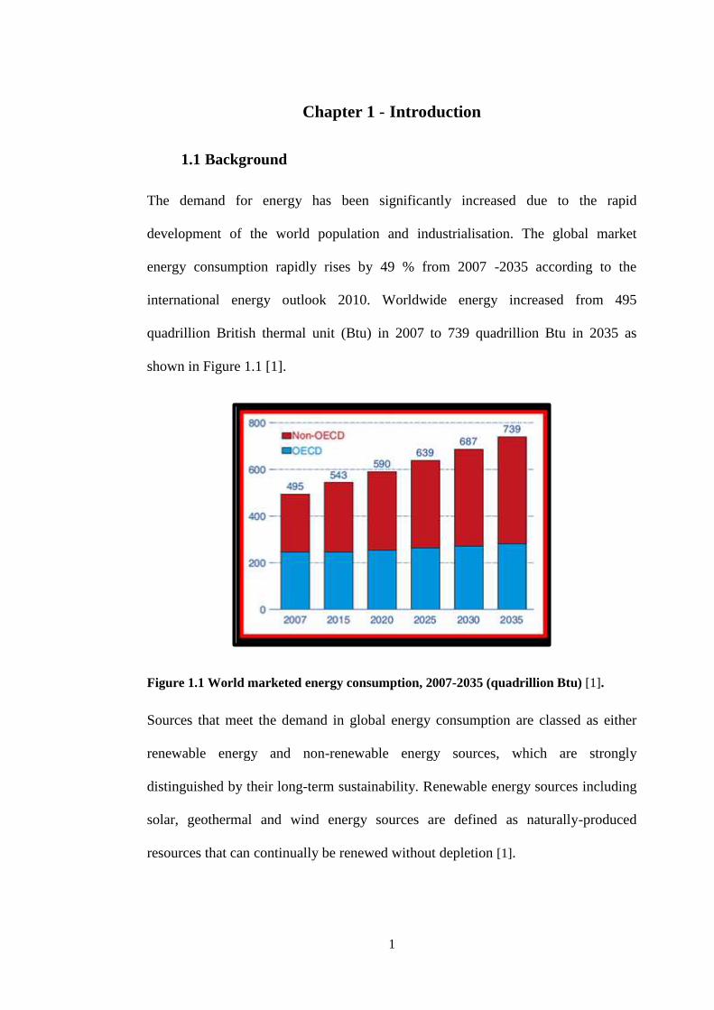
international energy outlook 2010. Worldwide energy increased from 495
quadrillion British thermal unit (Btu) in 2007 to 739 quadrillion Btu in 2035 as
shown in Figure 1.1 [1].
Figure 1.1 World marketed energy consumption, 2007-2035 (quadrillion Btu) [1].
Sources that meet the demand in global energy consumption are classed as either
renewable energy and non-renewable energy sources, which are strongly
distinguished by their long-term sustainability. Renewable energy sources including
solar, geothermal and wind energy sources are defined as naturally-produced
resources that can continually be renewed without depletion [1].

2
On the other hand, non-renewable energy resources are defined as being finite by
nature as they deplete long-accumulated fossil-based materials such as oil, natural
gas and coal as well as natural elements which are used to generate nuclear energy.
Figure 1.2 shows that fossil fuel are still the greatest source for energy production
and are dependent upon the requirments of the expanding energy demand between
2007 and 2035, which may lead to a depletion of these resources after a finite
period. In addition to the factor of being finite, the increase in carbon dioxide
emissions as a result of burning fossil fuels is further raising concerns on global
climate changes which results in increasing hazard to human beings worldwide.
Figure 1.2 World marketed energy use by fuel type, 1990-2035 (quadrillion Btu) [1]
When compared to traditional forms of fossil fuels, nuclear energy is the most
feasible alternative as very large amounts of energy can be generated without
producing CO2 emissions. However, the presence of potential leakage among
nuclear plants and the disposal of nuclear waste is always an ongoing concern to
worldwide energy producers. By contrast, alternative renewable energy sources are
non-destructive to the environment and unlike fossil fuel sources, they cannot be

3
depleted. These include solar, wind, and geothermal energy sources. The use of fully
renewable sources presents an enormous opportunity to preserve the environment
and positively impact on human health. As one of these renewable sources, solar
energy is promising and has attracted a significant of attention during the last decade
due to its following favourable advantages:
1. Abundance, sustainability of the source, and non-destructive impact on
the environment.
2. It has the lowest demand of maintenance and guarantees a long-term
performance of up to 20-25 years for Si-based solar cells.
3. The potential to install solar cells at remote locations, rendering it
unnecessary to be connected to the national grid.
4. Significant cost-reduction seen in solar panels, from $76/Watt in 1977 to
only 0.35 cent/Watt in 2015 as shown in Figure 1.3.
Figure 1.3 Price history of silicon PV cells in US$ per watt [2]

4
1.2 The solar radiation and air mass
The sun, being our closest star, is a spherical body emitting large amounts of solar
radiation onto the earth surface via the void of empty space. The approximate
distance between the sun and the earth is 2.4×10¹¹ Km. It has been calculated that
the sun supplies energy to the earth at 1.08×10¹⁷ W [3,4], whilst the yearly global
energy consumption is calculated at approximately 1.78×10¹³ W [5] . Based on these
calculations, only a very small proportion of the energy emitted by the sun is
required to meet a year’s global energy demand.
The solar spectral distribution is defined as the feasible relationship between the
intensity of solar radiation and the wavelength [6]. Moreover, the solar spectral
distribution is altered when the radiation penetrates the earth's atmosphere through
scattering and absorption [6].
However, before the sun’s radiation reaches the surface of the earth, this process
begins with the fusion of hydrogen and helium at the sun’s interior, creating a core
temperature of approximately 1.5 ×10⁷ K. Furthermore, as this process moves
through the layers of the star, the solar radiation emitted from the sun’s surface layer
and close to that emitted out into space has a temperature of around 6000 K [7]. The
spectrum of electromagnetic solar radiation includes γ rays, X-rays, ultraviolet
radiation, visible light, infra-red radiation, radio waves and radar waves [8]. From
these emissions, two main properties of the sun may directly impact on the solar
cells units; irradiance which is the proportion of fallen radiation on the surface per
unit area; and the characteristic spectra of the radiation [9]. Furthermore, it should
also be mentioned that the sun’s position continuously changes each day,
subsequently changing the distance of the sun’s irradiance between the sun and the

5
earth’s surface. Because of this fluctuation, the level of attenuation can vary
drastically. This factor is determined by the air mass.
Air mass (AM) could be defined as the required distance for solar radiation to travel
to the earth's atmosphere, which impacts on both the irradiance and solar spectral
distribution [10] as shown in Figure 1.4.
AM0 refers to the solar radiation spectrum outside of earth’s atmosphere meaning
that the path length within the atmosphere is zero [11].
AM1 refers to the distance of the solar radiation spectrum required to reach the
earth’s surface when the sun is directly at an overhead position relative to the earth.
AM 1.5 occurs when the solar radiation has a solar zenith angle (ȥ) at 48.2° from the
overhead position. Moreover, the Solar Zenith angle (ȥ) could be defined as the
angle between the sun and the vertical [10].
Figure 1.4 The path length, in units of Air Mass (AM) measured at a condition AM0, AM1 and AM 1.5

6
1.3 Motivation for research
The first and second generation of solar cells based on the mono-crystal silicon and
thin film silicon respectively have a very high efficiency making them commercially
viable for a long time. However, their high fabrication cost as well as technology
complexity lead to numerous investigations on lower cost solar cell technologies
that could provide inexpensive and efficient alternative PV devices [12]. Recently, a
new generation of solution-processable photovoltaic devices (SPPDs) has become
prominent which mainly includes dye-sensitized solar cells [13], quantum-dot solar
cells [14], polymer solar cells (PSC) [15], and very recently perovskite solar cells
[16]. They have the required features of ease of fabrication, cost effectiveness,
possibility of using flexible substrates, and large area device processing using roll to
roll (R2R) technology or other simple solution manufacturing methods [17–20]. The
simplicity of the fabrication processing technologies of SPPDs potentially results in
a sharp reduction in the cost of large-scale photovoltaic devices.
Amongst these solar cell technologies, PSCs appear to be one of the most promising
candidates in the competition to achieve low-cost photovoltaic devices due to their
advantage of being lightweight, ability of deposition on flexible substrates and
simplicity of fabrication process. However, in spite of these promising advantages,
the performance of PSCs does not exceed 11.7% for the single bulk heterojunction
[21]. Furthermore, hybrid organometal halide perovskite has recently received
substantial consideration as an inexpensive photoactive alternative material to the
conventional Si-based solar cells. Amongst the superior properties of this material
are its direct band gap, high absorption coefficient and long electron-hole diffusion
length with the highest efficiency of more than 22% [22]. In spite of the excellent
performance of perovskite solar cells, further investigations are still required to

7
solve the major issues of stability of the perovskite materials and the toxicity of lead
(Pb).
1.4 Aims and objectives
The primary aim of this research is to develop low cost, highly stable, and highly
efficient solution-processed photovoltaic devices using both dip- and spin- coating
methods. The current research objectives are focussed on fabricating three different
structures of solar cells based on photoactive polymer, organometal halide
perovskite, and hybrid photoactive polymer-perovskite composite using solution
processed techniques via either dip- or spin- coating methods. Dip-coating technique
has been used to fabricate high performance photoactive polymer solar cells. The
solutions for each layer in the polymer solar cells were modified in order to be
compatible with the dip-coating method for producing PV devices.
On the other hand, two step spin coating method (TSSCM) has been employed to
produce high-efficiency perovskite solar cells using [6,6]-phenyl C61 butyric acid
methyl ester (PCBM)-based planar heterojunction structures. Moreover, three step
spin coating method (THSSCM) has been used to fabricate a novel photoactive
composite structure based on perovskite-PTB7 materials to achieve high
performance with enhanced stability compared to solar cells fabricated from the
pristine perovskite. Several techniques have been utilised in this research in order to
analyse the produced thin films and devices; these include:
UV-vis spectroscopy and X-ray diffraction patterns are used to examine
the optical and structural properties of the thin films respectively.
8
Atomic force microscopy (AFM) and scanning electron microscope
(SEM) are used to investigate the surface morphologies of the produced
thin films.
FTIR and photoluminescence PL are utilised to examine the internal
structures of the composite perovskite and optical properties respectively.
Current density-voltage (J-V) characterisation and external quantum
efficiency (EQE) measurements are carried to identify the performance
of produced solar cells.
1.5 Outline of the thesis
This thesis is organised as follows:
In Chapter 2, a literature review is carried out to better understand current
technologies, manufacturing and developing of solar cells. Basic
architectures of solar cells and fabrication methods are reviewed.
Furthermore, present issues with solar cell technologies and methods to
combat these issues are also presented.
Chapter 3 introduces the selection and preparation of materials used in this
thesis (i.e. photoactive materials, electron transport materials, hole transport
materials, and electrodes), and study of their features and their
characteristics. This chapter also introduces the principles of various
characterisation techniques used in this work.
In chapter 4, the fabrication of polymer solar cells using dip coating method
is discussed. AFM is used to investigate the morphology of the photoactive
layer, hole transport layer and electron transport layer fabricated using either

9
dip or spin coating method, separately. UV-Vis absorption spectroscopy and
X-ray diffraction measurements are also be used to examine the optical and
structural properties of the photoactive layer.
Chapter 5 explains the use of the one-step spin deposition method (OSSDM)
to fabricate perovskite materials. The top surface morphology, the optical
and crystal structure properties of the perovskite film fabricated via OSSCM
will be studied. The two-step static deposition method (TSSDM) is used to
fabricate the perovskite thin films. Extensive investigations are carried out
to examine the perovskite films morphologies and crystallisation behaviour
by altering different parameters. Moreover, the prepared perovskite films
will be characterised using UV-Vis absorption and X-ray diffraction tests to
understand their optical and structural properties. The impact of thermal
annealing treatment on the perovskite films will be examined using the
optimized parameters.
Building on the ideal parameters identified in the previous Chapter, Chapter
6 investigates the fabrication of highly efficient reproducible perovskite
solar cells with varying concentrations of Methylammonium iodide (MAI)
solution using TSSCM. The optical and structural properties of the
perovskite films will be examined when different concentrations of the MAI
are used. Moreover, the cross section and the top surface morphologies of
the perovskite films under these concentrations of the MAI solution will be
assessed.
In Chapter 7, a novel photoactive material based on conjugated photoactive
polymer and a nanocomposite halide perovskite is developed. This new light

10
harvesting layer employs to fabricate highly efficient hybrid solar cells.
Blending the conjugated photoactive polymer with the perovskite extends its
light absorption and significantly enhances the solar cells’ stability up to
940 hours inside the glovebox compared to the pristine perovskite-based
solar cells. Their optical and structural properties examine using UV-Vis
absorption and photoluminescence as well as X-ray diffraction. The surface
and cross section morphologies of the novel photoactive absorber studies
using AFM and SEM. Additionally, stability of solar cells fabricated from
the pristine perovskite and the novel composite material investigates under
the condition of storing in a glovebox for a time period.
Lastly, Chapter 8 presents conclusions derived from this work and the
implications for future research will also be addressed.

11
Literature Review Chapter 2 -
2.1 Introduction to solar cells
Photovoltaic (PV) technologies may trace back to more than one hundred years ago.
In 1839 French scientist Edmond Becquerel [23] first noticed the photovoltaic effect
after two metal electrodes were placed in an electrolyte. In 1873 and 1876
respectively, Smith and Adams discovered the photoconductivity of a solid material
known as selenium [24]. Although the selenium did not work as a PV material, there
was an important benefit derived from this experiment which showed that solid
materials might convert light into electricity without heating. More than seven
decades later, the first photovoltaic cell based on silicon p-n junction was revealed in
1954 in the Bell labs in the United States [25].
Chapin, Fuller, and Pearson observed the sensitivity of silicon doped with an
impurity to light [26,27] which has resulted in power conversion efficiency (PCE) of
~6%. Since then, scientists have endeavoured to implement a series of developments
for manufacturing high-efficiency Si-based solar cells with a high degree of
stability. As a result, the highest efficiency of solar cells reached 25% and they have
since dominated the market [28].
However, the production of high-purity Si requires high-temperature, a very clean
environment, and high-cost equipment. As a result, there was an urgent necessity to
find alternative materials which can be manufactured at low cost without employing
complicated fabrication processes. Although amorphous silicon, cadmium-telluride,
copper indium gallium diselenide (CIGS) thin films-based solar cells fabricated by
vacuum deposition methods were discovered with lower fabrication cost than Si-

12
based solar cells. The PCEs of solar cells produced from these materials are still
smaller than that of bulk Si-based solar cells. Their highest reported efficiencies
were ~10.1%, ~16.7%, and ~19.4%, respectively [28].
Compared to the vacuum-based methods, solution-processed solar cells have
significantly reduced cost using R2R method and showed potential to revolutionise
thin film-based solar cells. Polymer-based, organometal halide perovskite-based,
and kesterite-nanoparticles-based (e.g. Cu2ZnSn(S,Se)4) solar cells are able to be
fabricated by the solution-processed method. The PCE for polymer-based and
kesterite-nanoparticles-based solar cells has increased to around 11% [21]. Halide
lead perovskites presented very promising results for light harvesting, which led to a
significant achievement PCE of better than 20% in a short period [29].
Semiconductive polymers such as poly (sulphur nitride) and polyacetylene were first
investigated in solar cells in the 1980s [27]. However, the achieved PCE was limited
to less than ~0.1%. In 1986, a significant transformation occurred when Tang used
heterojunction structures (copper phthalocyanine (CuPc) as a donor and a perylene
tetracarboxylic derivative as an acceptor) in one cell [30] with PCE increasing
significantly to ~1%. This transition opened the door of exploring the use of cheap,
lightweight, and flexible materials to produce solar cells. Progress was realized in
1995 when the first bulk heterojunction (BHJ) PV device from semiconductive
polymers was invented by Heeger's group and Friend's group separately [31,32].
Since then, studies have been carried out and efforts have been intensified over the
past twenty years to developing PSCs.
This chapter will review different photoactive materials which were used to
fabricate low cost solution processed solar cells mainly including semi-conductive

13
polymers with fullerene derivatives and organolead halide perovskites. Different
fabrication methods, architectures, and solar cells development will be reviewed.
2.2 Generation of solar cells
The first-generation of solar cells were based on wafers of the monocrystalline or
polycrystalline silicon. Currently, they still dominate nearly 90% of the commercial
solar cell market [27]. They typically exhibit features of high stability and efficiency
(PCE of ~25% for monocrystalline Si-based solar cells and ~20% for poly-
crystalline Si-based solar cells respectively [28]. However, there are some
limitations for Si-based solar cells including their high installation costs, the costly
production of high purity silicon wafers and relatively low visible light absorption if
compared with other semiconductors.
Drawbacks within the first generation solar cells led to the development of the
second-generation PV devices that were based on the thin film solar cell
technologies [25]. The candidate materials for the second-generation solar cells are
amorphous silicon, cadmium telluride (CdTe) and copper indium gallium selenide
(CIGS). The fabrication processes for the second-generation PV devices including
sputtering, physical and/or chemical-vapour deposition methods have been widely
used [33]. The attainable PCE of around 15-20% was achieved for the laboratory
prototype PV devices, demonstrating their potential to compete with the silicon-
wafer-based PV devices [33].
Despite the significant reduction in the cost of thin film solar cells, the PCE of the
second-generation solar cells is still lower than that of the first- generation solar
cells [34]. One of the main disadvantages for the second-generation solar cells based
on (CdTe) and (CIGS) is either the high-temperature fabrication or the need for high

14
vacuum technology. Additionally, some raw materials used in the second-
generation solar cells are scarce, expensive (e.g. indium), very toxic (e.g. cadmium),
and unstable [35].
Because of these drawbacks, a so-called third-generation of solar cells by the
solution-processed methods has emerged [36]. The benefits of the first and second-
generation PV devices are still in the foreground, which attracts the global market
due to their high degree of stability and high performance. Nevertheless, because of
limitations of the complicated production processes and excessive cost, they are not
able to compete with low-cost electricity generated by burning fossil fuels. Thus, it
is necessary to develop inexpensive PV devices to compete with the fossil fuels
energy.
Solution-processed solar cells have the potential to be produced at very low-cost.
Polymer-based semiconductive materials have the potential to be used to fabricate
PV cells at low temperature through the high throughput solution-processed method
[37]. Polymers are typically considered the cheapest materials and have high
absorption coefficients, allowing them to form very thin films, typically a few
hundreds of nanometres [38]. By using these materials, the cost of PV cells will be
reduced considerably; however, the performance needs to match their first and
second-generation counterparts. The highest achieved power conversion efficiency
of polymer solar cells is currently at ~11.7% [21]. Very recently, a new-type of
solution-processed organic-inorganic hybrid halide perovskites have been developed
and an efficiency of ~22.1% has been achieved [39].

15
2.2.1 Operational mechanisms of photovoltaic solar cells
The mechanisms of absorbing photons in semiconducting polymer based solar cells
and generation of free charge carriers followed by their collection at both electrodes
could be categorized into six main steps as shown in Figure 2.1 [40].
These steps are:
1- Absorption of photons and creation of excitons
2- Exciton diffusion
3- Exciton dissociation
4- Charge carriers separation
5- Charge migration
6- Charge collection at the electrodes
Figure 2.1 Schematic diagram of the main steps of the photocurrent generation in polymer-based solar cells

16
The working mechanism of polymer and organometallic halide perovskite solar cells
is shown in Figure 2.2. Typically, when the photovoltaic devices is exposed to the
incident sun light, the photons will penetrate through the different transparent layers
(e.g. ITO and PEDOT:PSS) before reaching the photoactive layer. Several factors
affect the proportion of generated excitons which are successfully dissociated and
collected by the corresponding electrodes including, the thickness of the photoactive
layer, the band gap of the photoactive layer, optical and other physical
characteristics of the hole and/or electron transport layers [41].
Among those factors, the band gap of the polymer or organometal halide perovskite
materials is the most important factor which determines the portion of incident
photons that will be absorbed by the active layer. For example, the band gap of the
photoactive layer of a organometal halide perovskite material is roughly 1.52-1.59
eV resulting in absorbed proportion of nearly 60% of the incident photons [42].
Figure 2.2 The processing mechanism of conversion photons into electricity in: a) Planar heterojunction Perovskite, b) Bulk heterojunction polymer solar cell
Only 30% of the incident photons are absorbed by a polymer-based photoactive
layer owing to the band gap of the majority of semiconducting polymers being

17
higher than 2 eV [43]. Moreover, absorption coefficients of polymer materials and
organometal halide perovskites are high ~105 cm-1 and 1.5×104 cm-1 at 550 nm
respectively [44].
The high absorption coefficient allows very thin film of the photoactive material at ~
100-300 nm of thickness to absorb most incident photons [40].
As a result of photons absorption in the photoactive layer of polymer with energy ≥
the band gap (Eg), electrons will be induced from the HOMO level to the LUMO
level forming a strong electrostatically bond electron-hole pair known as Frankel
excitons. On the contrary, in perovskite based solar cells, free charge carriers will
generate directly after absorbing photons in the photoactive layer with energy ≥ than
the band gap (Eg) of the active layer [45]. The excitons created in halide perovskites
are called Mott-Wannier which has very low binding energy at ~2 meV [46] unlike
photoactive polymer materials which has the Frankel exciton with high binding
energy at ~ 0.5 eV [40].
The Frankel exciton diffuses to the interfacial layer between the donor and the
acceptor. The diffusion length in polymer materials is in the range of 10-20 nm,
which leads to the requirement of bulk heterojunction structures between the donor
and the acceptor for efficient PV devices to prevent the recombination of free
electrons and holes. On the contrary, it is unnecessary to have bulk heterojunction in
halide perovskite-based solar cells and planar heterojunction structures are used to
obtain efficient PV devices. The halide perovskite materials have long diffusion
lengths of excitons of ~100 nm for CH3NH3PbI3 and ~1 m for CH3NH3Pb3-XIX
[47,48]. The generated excitons in polymer materials which diffused to the interface

18
between the donor (D) and the acceptor (A) remain electrostatically bond together
and an additional force is required to break the excitons into free charges [34].
The dissociation of charges at the D/A interface in polymer materials requires a
driving force due to high binding energy of excitons in polymers. The required
driving force for exciton dissociation is the internal electric field that can be
determined from the gradient in the potentials of electrons and holes in the D/A
interface. This internal electric field depends on the offset between the HUMO of
the donor and the LUMO of the acceptor [49]. The difference in work functions of
electrodes creates an external driving force to move and collect the free charge
carriers to the corresponding electrodes [50].
2.3 Polymer-based solar cells
2.3.1 Development of polymer solar cells
The first attempt to produce polymer solar cells was in 1959 when an anthracene
single crystal was used [51]. Since then, considerable efforts have been made and
studies have been carried out to find highly efficient and inexpensive materials for
PV devices which can compete with solar cells based on inorganic materials. The
polymer materials have various desirable characteristics including high flexibility
and simple fabrication processes using lightweight, low-cost and simple to produce
raw materials [17–20]. Moreover, polymer materials have very high absorption
coefficient compared with inorganic materials such as Si, which offer an opportunity
to produce very thin film devices [38]. The active layer in polymer solar cells is
based on donor and acceptor materials. The donor has a low ionisation potential, and
the acceptor has a high electron affinity (χs) [34]. In the last decade, two types of
materials have been used extensively in the preparation of PV cells active layer.

19
These are P3HT and PCBM as the electron donor and the electron acceptor
materials, respectively. Their outstanding performance and high stability make them
distinct obvious choice for a current scientific research [52]. In photoactive polymer
materials, the optical band gap is in the range between ~1.4 eV to ~2 eV [53].
The solution processed polymer-based solar cells have attracted outstanding
attention as a favourable alternative to the classical inorganic Si-based solar cells
due to their lightweight, inexpensive raw materials, and the possibility of producing
solar cells on a large-scale R2R technique. Following the emergence of bulk
heterojunction structures in polymer solar cells in 1995 [31], many researchers were
focused on the development of increasing the PCE of polymer solar cells. Shaheed
et al. claimed a bulk heterojunction structure when he applied the mixture of
poly[2-methyl,5-(3*,7**dimethyl-octyloxy)]-p-phenylene vinylene (MDMO-
PPV):PCBM as an active layer. He used the spin coating method to deposit the
active layer and a PCE of ~2.5 % was achieved [54]. The blend of P3HT:PCBM as a
photoactive layer in the polymer solar cell was presented by Chirvase et al. in 2003.
They mixed P3HT: PCBM at the weight ratio of 1:4 as a photoactive layer and
~0.2% PCE was obtained [55]. Pandinger and co-workers increased this PCE
performance to ~3.5% when they blended P3HT:PCBM at 1:1 weight ratio. The
performance of the device was enhanced after thermal annealing was applied for
several minutes to the whole device [56]. Over the years, the power conversion
efficiency had remained between 3-5% [57] until 2011 when Mitsubishi Chemical
manifested a high PCE of ~10.0% [58]. However, no details regarding the
photoactive materials and the device architecture were given [58]. In 2013, a high
fill factor between 75-80 % and PCE of 8.7% was achieved for the single junction
structure by using poly[5-(2-hexyldodecyl)-1,3-thieno[3,4- c]pyrrole-4,6-dione-alt-

20
5,5-(2,5-bis(3-dodecylthiophen-2-yl)-thio- phene)] (PTPD3T) or poly[N-(2-
hexyldodecyl)-2,2 -bithio-phene-3,3 -dicarboximide-alt-5,5-(2,5-bis(3-
decylthiophen-2-yl)- thiophene)] (PBTI3T) as donor polymers blending with
PC71BM as the acceptor material. The enhanced fill factor and performance of the
highly ordered BHJ bicontinuous networks give optimum vertical phase gradation
and very close packing. These contributions result in higher extraction and life time
[59].
In the same year, Yang and co-workers claimed a high PCE of polymer solar cells of
10.6% via using tandem structure under the standard conditions [60]. They mixed a
low band gap polymer poly{2,6 -4,8-di(5-ethylhexylthienyl)benzo[1,2- b;3,4-
b]dithiophene-alt-5-dibutyloctyl-3,6-bis(5-bromothiophen-2-yl)pyrrolo[3,4-
c]pyrrole-1,4-dione} (PBDTT-DPP) with PCBM for the front photoactive layer and
P3HT:ICBA in the back photoactive layer. In 2015, J.D Chen et al. claimed a high
PCE for a single junction polymer solar cell, surpassing 10%. They utilised
nanoimprinting technology to blend deterministic aperiodic nanostructures (DANs)
into the single-junction polymer solar cells for broadband self-enhanced light
absorption with enhance charge collection. Blending of poly[4,8-bis(5-(2-
ethylhexyl)thiophen-2-yl)benzo[1,2-b:4,5-b ] dith- iophene- co -3-fluorothieno[3,4-
b]thiophene-2-carboxylate]:[6,6]-phenyl-C71-butyric acid methyl ester (PTB7):
PC71BM was used as a photoactive layer [61].
Also in 2015, Z. He et al. reported a high PCE (over 10%) for a single junction [62].
This high PCE was produced by controlling the tail state density under the
conduction band of the electron acceptor and the disorder stage of the mix produced
from a newly designed semiconducting polymer with a low band gap (1.59 eV) and
PC71BM. The narrow band gap semiconducting polymer was synthesized from 1.59

21
poly [[2,6 -4,8-di(5-ethylhexylthienyl)benzo[1,2-b;3,3-b] dithiophene] [3-fluoro-
2[(2-ethylhexyl)carbonyl]thieno[3,4-b]thiophenediyl]] (PTB7-Th) and mixed with
PC71BM as a photoactive layer [62]. Very recently, Prof Yan's group from South
Korea achieved a certified PCE of 11.5% and 11.7% in 2016 using an
environmentally friendly hydrocarbon solvent-based system [21] . To date, the bulk
heterojunction structure remains one of the most auspicious configurations of the
polymer-based solar cells.
2.3.2 Architectures of polymer solar cells
2.3.2.1 Bi-layer junction architectures
In 1986, C.W. Tang used two different materials as the donor and the acceptor with
different ionization potentials and electron affinities in the bi-layer heterojunction
structure as shown in Figure 2.3 [30,32]. Copper phthalocyanine (CuPc) was used as
the donor and perylene tetracarboxylic derivative as the acceptor. The required
electric field that contributes to dissociate charge carriers effectively was created by
the band offset at the donor-acceptor interface. The power conversion efficiency of
this device was only ~1%. After excitons diffuse to the interface between donors and
acceptors and dissociated electrons and holes will migrate in the opposite direction
to their respective electrodes, which requires a long carrier life time so that they can
reach the electrodes before recombination [63].

22
Figure 2.3 Schematic diagram of the planar heterojunction structure
2.3.2.2 Bulk heterojunction
In the bilayer heterojunction of PSCs, the short circuit current and power conversion
efficiency are usually very low because most charge carriers decay or recombine
before collection by electrodes. The reason is that free charge carrier mobility and
exciton diffusion length in photoactive polymers are much lower compared with that
in inorganic materials [51]. This led to the discovery of the concept of bulk
heterojunction structures by Yu et al. in 1995 [31].
The idea of bulk heterojunction structures is based on increasing the interfacial area
between donors and acceptors in tens-nanoscale phase separation and reducing the
dissociation length of charge carriers. After its discovery, substantial progress was

23
made in the development of polymer solar cells [32]. The bulk heterojunction
structure is formed after an interpenetrating donor mixes together with the
bicontinuous network of the acceptor as shown in Figure 2.4. Excitons can then be
created anywhere in the active layer, resulting in an increased number of arising
pathways in the donor and acceptor from their interfaces to the corresponding
electrodes. Consequently, an excessive number of charge carriers will percolate to
both electrodes via the introducion of charge transport pathways. It is very important
that a percolating pathway is required in the bulk heterojunction structure of PSCs in
order to facilitate the transition of the separated charges to both electrodes [64].
Figure 2.4 Schematic diagram of the bulk heterojunction organic solar cells
The introduction of BHJ structures in PSCs contributes to increase short-circuit
current and fill factor, which leads to an increase in the PCE. After many efforts
have been exerted, an important factor has been studied in the PSCs, which is
morphology of the active layer. The latter plays the main role in optimising the
24
properties of the active layer and thus enhancing the performance of the solar cells.
There are many aspects affecting the morphologies of bulk heterojunction between
donor and acceptor materials; these include type of solvents used, ratio of
compounds between donors and acceptors, and layers annealing method [65]. One
of the most investigated materials in the field of BHJ polymer solar cells is P3HT as
the donor and PCBM as the acceptor due to their good performance and high degree
of stability [52]. The use of bulk heterojunction structures in PSCs has dramatically
increased the performance of solar cells. The PCE increased from ~5% in 2008 for
the single BHJ device to 11.7% by employing hydrocarbon-based processing system
in 2016 by Yan’s group [21] that is deemed more environmentally friendly
compared to the use of halogenated solvents.
2.3.2.3 Tandem solar cells
Considerable loss of energy is inevitable in a single BHJ PSCs stemming from an
inability to absorb photons with smaller or larger energy than the band gap of the
materials. Such loss can be reduced by using tandem solar cell architecture. The
concept of tandem solar cells is based on making the most from absorbing different
wavelengths of photons in the solar light spectrum while increasing light harvesting.
In contrast, a single active layer relies on absorbing photons in a specific wavelength
of the solar light spectrum. Tandem solar cells have a potential to acquire a wider
range of solar radiation by using materials with various absorption bands. The
architecture of tandem solar cells practically contains two separate subcell layers
connected in series. The open circuit voltage of tandem solar cells can be calculated
by summing the voltage value of each cell while the current is the same. Between
two active layers, there exists an interconnecting layer (ICL) which is a combination
of an electron transport layer (e.g. metal oxide) and a hole transport layer (e.g.

25
PEDOT:PSS) as shown in Figure.2.5. The ICL must be a strong protection layer to
prevent solvents from the upper layer penetrating into the lower layer. With the
invention of different low band gap photoactive polymers presenting wide
absorbance including near infrared light, the tandem structure is applicable and 10%
barrier in PCE has been transcended. In 2008, 8.62% PCE was achieved by Yang's
group for the tandem polymer solar cells, which has been further increased to 10.6%
in 2012 [60]. Four years later, the PCE of tandem polymer solar cells was increased
to over 11 % by Prof. Hou's group [66] after developing a new low band gap
polymer poly(2,5-bis(2-decyltet- radecyl)- pyrrolo[3,4-c]pyrrole-1,4(2H,5H)-dione-
3,6-diyl- alt - 3 ,4 -difl uoro-2,2 μ5 ,2 μ5 ,2 -quaterthiophene-5,5 -diyl (PDPP4T-
2F) used in a double junction tandem structure with either PC61BM or PC71BM.
Figure 2.5 A schematic diagram of the tandem bulk heterojunction structure

26
2.3.3 Fabrication methods of solution-processed solar cells
The first stage of transforming organic or organic-inorganic solution -processed
solar cells from the lab scale to commercialisation is to determine the deposition
methods that will offer mass production and low-cost. The roll-to-roll techniques to
fabricate polymer solar cells on low-priced and flexible substrates have a great
potential to significantly reduce the cost of solar cells. Currently, various techniques
including spin, doctor blade, spray, slot die, and other thin film coating methods
have been investigated in the lab scale. Future efforts will be made to transfer the lab
scale PV devices to industrial mass production. Different deposition methods have
their own advantages and disadvantages.
The spin-coating method is one of the most famous fabrication methods, which is
commonly used in the lab to fabricate solution-processed solar cells due to its
simplicity, low-cost, and repeatability. As shown in Figure 2.6, a limited amount of
solution with specific concentration drops onto the centre of the substrate during
rotation with a selected rotating rate. The solvents evaporate forming a uniform thin
film. The main advantage of the spin-coating method is that a very uniform and
homogenous thin film is produced while the solvents are drying. Several factors can
affect the thickness of thin films including spinning rate, solution viscosity, and
temperature [67].

27
Figure 2.6 Schematic of spin-coating process
The main limitations of using the spin-coating method relate to high levels of wasted
solution and the small-scale thin films are produced. Consequently, it is not
favourable for mass production [18].
Blade coating also called doctor blading or knife coating, is widely used to fabricate
large-scale thin film coating, as illustrated in Figure 2.7. There are several
parameters that can be adjusted to control the film thickness produced by blade
coating technique including blade gap, blade coating speed and concentration of the
solution [68]. The main advantages of using the blade coating technique are that it
gives large-scale surface uniformity, fewer waste materials, avoids interlayer
dissolution and it is compatible with (R2R) technique. However, the major obstacles
of using the blade coating technique are the complex chemistry of ink formulations
and the contact effects when the followed layer is applied on the previously formed
film [69].
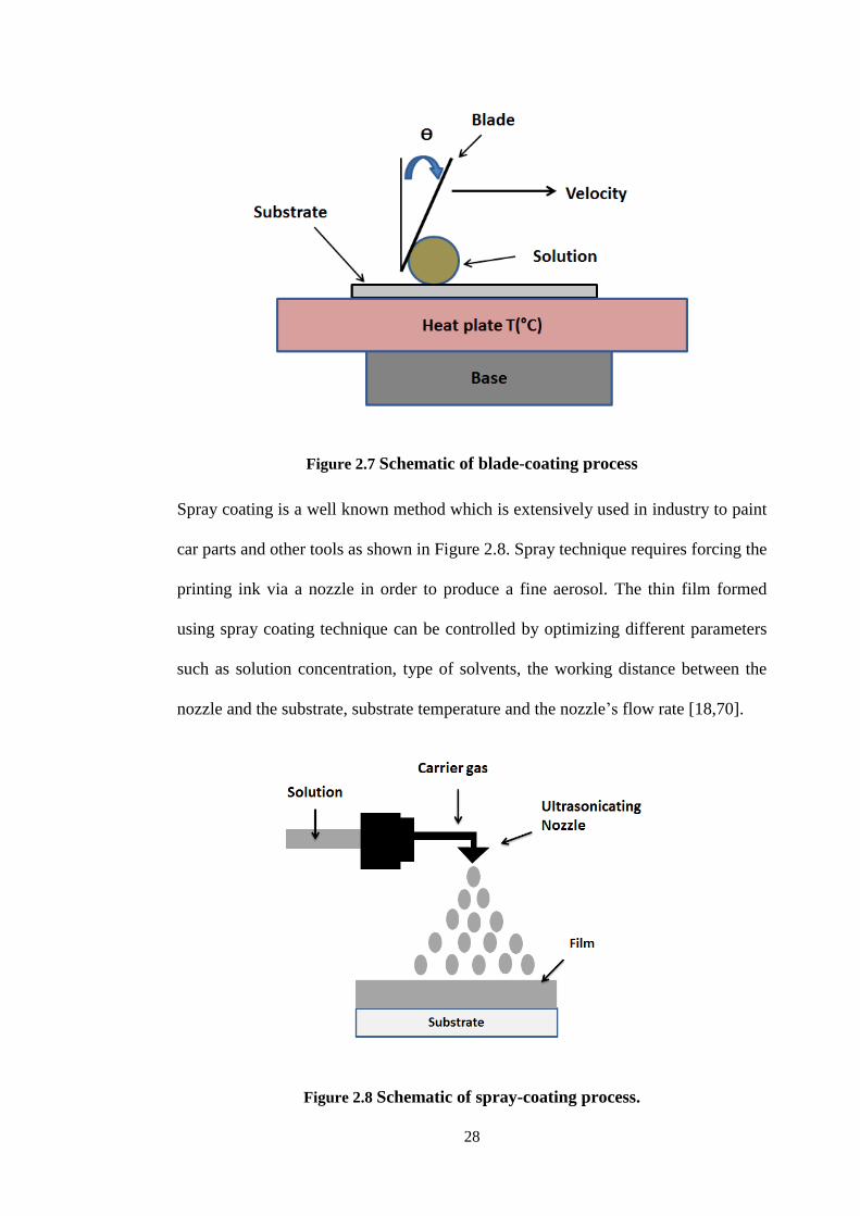
28
Figure 2.7 Schematic of blade-coating process
Spray coating is a well known method which is extensively used in industry to paint
car parts and other tools as shown in Figure 2.8. Spray technique requires forcing the
printing ink via a nozzle in order to produce a fine aerosol. The thin film formed
using spray coating technique can be controlled by optimizing different parameters
such as solution concentration, type of solvents, the working distance between the
nozzle and the substrate, substrate temperature and the nozzle’s flow rate [18,70].
Figure 2.8 Schematic of spray-coating process.
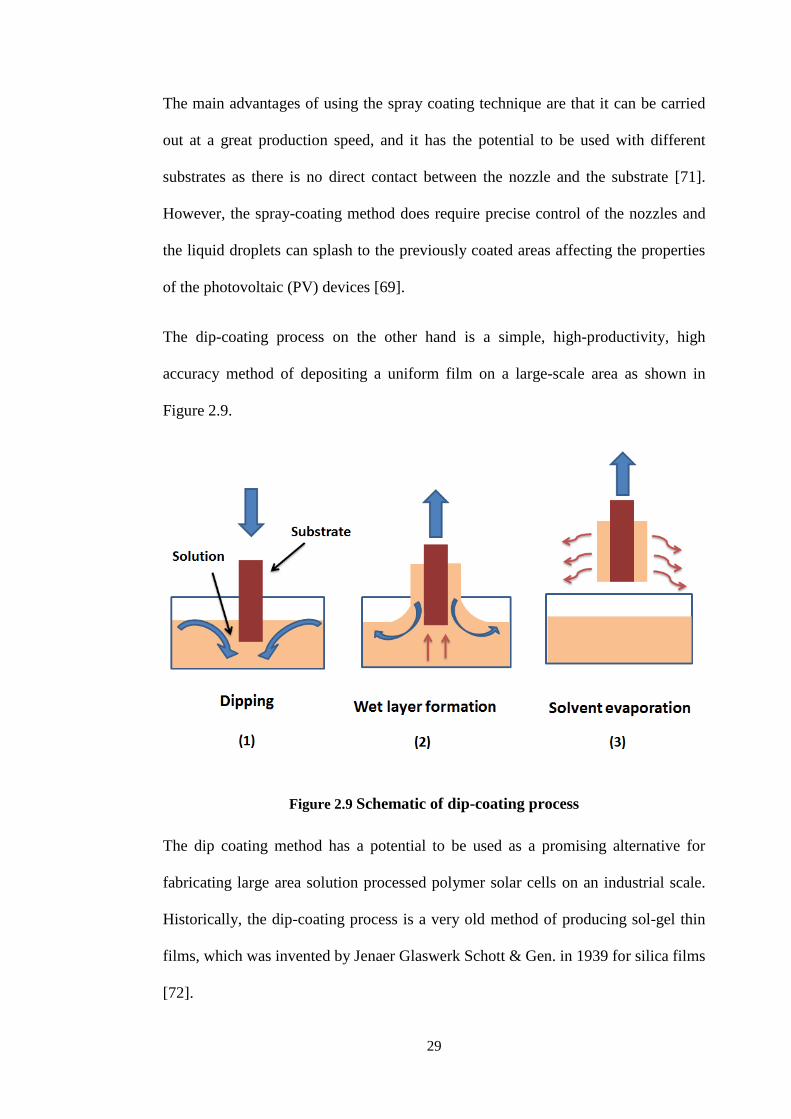
29
The main advantages of using the spray coating technique are that it can be carried
out at a great production speed, and it has the potential to be used with different
substrates as there is no direct contact between the nozzle and the substrate [71].
However, the spray-coating method does require precise control of the nozzles and
the liquid droplets can splash to the previously coated areas affecting the properties
of the photovoltaic (PV) devices [69].
The dip-coating process on the other hand is a simple, high-productivity, high
accuracy method of depositing a uniform film on a large-scale area as shown in
Figure 2.9.
Figure 2.9 Schematic of dip-coating process
The dip coating method has a potential to be used as a promising alternative for
fabricating large area solution processed polymer solar cells on an industrial scale.
Historically, the dip-coating process is a very old method of producing sol-gel thin
films, which was invented by Jenaer Glaswerk Schott & Gen. in 1939 for silica films
[72].

30
Nowadays, many commercial optical functional sol-gel thin films on glass have
been manufactured by the dip-coating method with a large area of several square
meters. Moreover, the dip-coating method significantly reduces the number of
wasted materials during processing and could be used to fabricate two PV devices at
the same time. The main disadvantage of the dip-coating method is that only rigid
substrates can be used.
Furthermore, different printing techniques have been developed after the printing
press evolved by Johannes Gutenberg in 1440 [17]. Although these printing
techniques have their own positive and negative aspects, they depend on the similar
process of moving the ink solution to the substrates [17].
(R2R) method is one of the important printing techniques which can be used for
commercial production of solar cells. Slot-die coating and knife coating are the two
most common techniques which incorporate the R2R method as shown in Figure
2.10. In the knife coating method, the ink tank is placed before the knife that acts to
provide the meniscus with new ink. When the substrate moves, the fixed knife
drives the ink in front of it only allowing ink that fits below the edge to pass
through. The two main parameters that could affect the thickness of the film
produced by the knife coating method are; i) the distance between the knife and the
substrate and ii) the speed rate of the roll. The knife coating method is appropriate
for coating large scale areas without any pattern [73].

31
Figure 2.10 Schematic of knife-coating process and slot-die coating
In the slot-die coating the coating head is placed very near to the substrate without
contacting it. The ink is injected via the fixed coating head into the moving substrate
creating a continuous coat on the large scale substrates [18]. It is possible to coat
different width of stripes using slot-die coating methods [18]. However, web speed
is limited during the operation of slot-die coating when applying the ink
composition. Exceeding this limit will stop the coating process [73].
2.3.4 Current limitations of polymer solar cells
Although the distinguished properties including inexpensive raw materials, solution
processed methods, and fabricating solar cells on flexible substrates make polymer
photoactive semiconductors privileged competitors with light-absorbing materials of
the first and second generation solar cells, - currently some limitations have
hindered their potential to achieve this goal. One of the main obstacles is the lower

32
power conversion efficiency when compared with the first and second-generation
solar cells. Moreover, the life span of polymer solar cells is short (less than one
year) compared with Si-based solar cells that have a life span of 25 years [74].
2.4 Organic-inorganic halide perovskite solar cells
2.4.1 Development of halide perovskite solar cells
Meeting the increasing energy demand is essential with the daily global growth and
development. Various PV technologies have emerged and gained a significant
attention as the promising energy sources including; dye-sensitized solar cells
(DSCs), polymer solar cells (OPV), and quantum dot (QT)-based solar cells.
Nevertheless, these solution-processed PV devices present much lower performance
when compared with the Si-based solar cells. The power conversion efficiency of
these solar cells were around 11% [45].
A promising candidate called organometal halide perovskites has recently emerged
as a novel and strong competitor in the PV community. It can be produced by the
solution-processed technique on flexible substrates [16]. The PCE of perovskite-
based solar cells jumped dramatically from ~3.9 to ~22 % just in a few years [75].
Currently, different fabrication techniques and configurations were used to fabricate
high efficiency perovskite solar cells. Miyasaka's group first utilised hybrid organic-
inorganic halide perovskites of CH3NH3PbBr3 with I-/I3- electrolyte in 2006,
reaching a PCE of 2.2%. The power conversion efficiency was improved in 2009 to
3.8% when they replaced Br with I [76,77].
Two years later, Im et al. increased the power conversion efficiency to 6.5% by
applying the spin-coated nanocrystalline perovskites onto the nanocrystalline TiO2

33
surface in the liquid electrolyte cells [78]. However, the lifetime of the liquid-
electrolyte-based perovskite solar cells was just a few minutes due to the prompt
decomposition of the perovskite material into the liquid electrolyte. This led to new
concept of replacing the liquid electrolyte by a solid-state hole transport material.
This was accomplished by Park and Gratzel in 2012 when they introduced the solid-
state solar cell instead of the liquid electrolyte [79]. They used spiro-MeOTAD as a
hole transporting material (HTM), the highest efficiency of 9.7% was obtained and
the stability of the devices was higher than that of the liquid electrolyte based solar
cell [79].
After replacing the liquid electrolyte, the power conversion efficiency of the halide
perovskite-based solar cell (CH3NH3PbI2Cl) reached over 10% as it adopted a
mesoporous structures [80,81]. Gratzel et al. developed a new structure of halide
perovskite solar cells with free hole transport material in the same year. The halide
perovskite acts as an absorber as well as a hole conductor. The structure was
(FTO/CH3NH3PbI3/ TiO2/Au) and PCE of 7.3% was achieved [82]. Snaith et al.
reported a new meso-supersaturated structure using mixed halide perovskite
CH3NH3PbI3-xClx as a light absorber and electron transporter. Replacing mesoporous
TiO2 by alumina oxide which worked as scaffold layer only, obtained a PCE of
10.9% [80].
Further improvement of PCE in the subsequent year was achieved when Gratzel et
al. presented the so-called sequential deposition technique of the perovskite active
layer within the porous metal oxide layer achieving a PCE of 15% [83]. At the same
year, Snaith and co-workers introduced very uniform morphologies of mixed halide
perovskite CH3NH3PbI3-xClx using a vacuum deposition technique. They obtained
thin film of perovskite directly on the substrate after controlling the evaporation

34
speed of two separate sources of thin film (PbCl2 and CH3NH3I); the produced solar
cell was shown to yield PCE of 15.7% [84].
The first certified PCE of halide perovskite solar cells of 14.1% was presented by
Gratzel in 2013. It was confirmed by two independent sources; solar cell efficiency
Tables compiled by Green et al. [85] and the National Renewable Energy
Laboratory (NREL)’s chart of research cell efficiency records. Furthermore, positive
results based on improving the structure of halide perovskite solar cells and
enhancing the morphologies of the photoactive films were reported. The certified
result jumped to 21.1% in 2015 by the Gratzel's group. Very recently, better power
conversion efficiency of 22.1 % was certified by NREL [86].
2.4.2 Properties of halide perovskites as light absorbers
2.4.2.1 Crystal structures of halide perovskites
Halide perovskites represent any material that has similar crystal structures to
calcium titanate (CaTiO3). In 1839, this mineral was discovered in Russia by Gustav
Rose and is named after the Russian mineralogist Lev Perovskite (1792-1856)
[85,87,88].
The general formula of a pure perovskite family is ABX3 as shown in Figure 2.11,
where A indicates a large cation and is located at the corners of the unit cell, B
indicates a smaller metal cation surrounded by six halide anions, creating six-fold
proportionate octahedrons, and X is an anion halide existing at the face centre
[89,90]. The initial discovery of halide based perovskites was in 1958 by Moller. He
found that the caesium lead halides (CsPbX3) have the perovskite structure [91].
Two decades later, the organic methylammonium cation appeared in halide based
perovskite structures produced by Weber and Naturforsch [92].

35
Figure 2.11 Crystal structure of halide perovskites
The perovskite crystal structure might be approximated by the tolerance factor (TF)
[87,93] which is identified as the proportion of the distance between A-X to the
distance between B-X; It could be given as [94]:
� = +√ + � …………………………………………… (2)
where RA, RB, and RX correspond to atomic radii of A, B and X respectively. The
ideal cubic geometry of perovskite could be obtained if TF =1 [95]. On the other
hand, if TF is less than 1, the octahedron [BX6] tends to be distorted to a low-
symmetry structure in order to keep the stability of the structure [95]. This degree of
distortion of the crystal structure could determine numerous physical features;
magnetic, electronic, and dielectric properties in particular [85].
The tolerance factor (TF) represents the essential guidance of stability, distortion,
and tuning of radii size of the perovskite structure [93]. In addition to tolerance
factor, chemistry and bonding play an important role on the formability and stability
of the perovskite structure [87,93]. The crystalline formation of perovskites possibly
36
depends on the temperature; for instance, the orthorhombic phase is formed at a low
temperature, which consecutively changed into the tetragonal and cubic structures
after increasing the temperature [96].
The perovskite materials show a direct band gap of ~1.5 eV for CH3NH3PbI3 to 2.2
eV for CH3NH3PbBr3, which might be tuned in an extensive range [97]
2.4.2.2 Electronic structure
Recent studies on the cubic phase of halide perovskite at room temperature have
disclosed that the characteristics of Pb-X determine the electronic structure of halide
perovskites [96]. The electronic structure of halide perovskites have indicated that
the valence band minimum (VBM) consists of σ antibonding states of Pb 6s and xp
orbitals and the conduction band maximum (CBM) primarily consists of σ-
antibonding states of Pb 6p orbitals and xs orbitals [98]. The contribution of MA
toward the electronic properties are too small as a result of the deep level of MA
structure within the valence and conduction band [99].
The cubic phase of MAPbX3 demonstrates that its electronic structure is mainly
controlled by the characteristics of the Pb-X bonds. The generalised gradient
approximation was used by Baikie's group to measure the band structures for three
phases of MAPbI3; i.e. cubic, tetragonal and orthorhombic phases [100]. It was
found that MAPbI3 has a direct band gap of 1.3 eV at the R point for a cubic
structure, 1.43 eV at the T point for tetragonal structure, and 1.61 eV at the T point
for the orthorhombic structure [100].

37
2.4.2.3 Optical structure and band gap
The prominent features of halide perovskites are the direct band gap and strong
optical absorption coefficient which render them highly attractive for use as
competitive absorbers in solar cells [82,101–103].
The perovskite materials present a broad absorption spectrum along the entire
visible to near-infrared range and have a large absorption coefficient compared to
conventional semiconducting materials. The absorption coefficient of organometal
halide perovskites is approximately1.5×104 cm-1 at 550 nm [79]. The absorption
properties of the MAPbI3 thin film was assessed and compared with other inorganic
semiconducting materials such as GaAs, CdTe, and CIGS which have the absorption
coefficient of up to 104-105 cm-1 [104]. The absorption onset edge of the perovskite
was nearly similar to these materials [104].
The band gap of the CH3NH3PbI3 was calculated to be 1.5-1.55 eV, resulting in a
limited absorption range of 800 nm or less. Consequently, tuning the band gap of
CH3NH3PbI3 is required to increase the absorption of photons of longer wavelengths
without affecting the absorption coefficient.
Absorbance of halide perovskites can be extended via tuning the band gap of
perovskite in order to enhance the performance of the halide perovskite-based PV
devices [85,104]. One of the strategies of tuning the band gap is to change
(CH3NH3I) MA with other organic or inorganic cations. For instance, by replacing
methylammonium with formamidinium which results in reducing the band gap by
0.07 eV [104]. Another way to achieve band gap tuning is to replace Pb with another
metal (partially or completely). For example, partially substituting Pb with Sn and

38
varying the ratio of Sn: Pb tunes the band gap between 1.17 eV and 1.55 eV in the
synthesis process of halide perovskites [105].
2.4.2.4 Key parameters for PCE of halide lead perovskite-based solar cells
Exciton binding energy (Eb) is one of the major factors that contribute to the
photovoltaic mechanism in organometal halide perovskite solar cells. The exciton
binding energy is controlled by the dielectric constant of the materials [106]. It is
noted that dielectric constant is very high in organolead halide perovskites compared
with photoactive polymers. Dielectric constant is nearly 32 [107] for halide
perovskites and is ~ 3 for photoactive polymers [108]. There are many ways to
determine the exciton binding energy including theoretical analysis [46], optical
absorption [109], magneto- absorption [110] and temperature dependence [111].
A theoretical analysis was used by Hirasawa in 1994 to calculate the exciton binding
energy in CH3NH3PbI3. He found that the exciton binding energy was estimated to
be 37meV [110]. Low binding energy in CH3NH3PbI3 suggests that excitons in
CH3NH3PbI3 are Mott-Wannier type excitons. On the contrast, the photoactive
polymers have high exciton binding energy which is estimated in the range of (0.3-
0.5 eV) [112] suggesting that excitons in photoactive polymers are of Frankel type.
Theoretical studies suggested that the Mott-Wannier excitons yield free charge
carriers at room temperature owing to the optical phonons and collective rotational
motion of the organic cations[113].
Consequently, low binding energy of solar light harvesting materials plays an
important role in achieving high PCE solar cells. Another important feature for
halide lead perovskites is their long carrier diffusion length related to charge
transportation properties compared with short diffusion length in photoactive

39
polymers. The long diffusion length can contribute directly to high-performance in
solar cells. The charge transport properties of CH3NH3PbI3 and CH3NH3PbI3-XClX
were studied separately by Xing et al. and Stranks et al.[47]. Each of these groups
conducted time-resolved photoluminescence (TRPL) and transient absorption
spectroscopy respectively. According to their results, it was estimated that the
charge diffusion length in CH3NH3PbI3 is ~100 nm and ~1 m for CH3NH3Pb3-XIX
compared with photoactive polymer materials with diffusion length of ~10 nm [47].
Bai et al. suggested that the charge carrier diffusion length of organometal lead
iodide is significantly reliant on the processing conditions and the deposition
techniques [114]. Two main factors determine the value of the diffusion length,
which are diffusion coefficient ( and carrier life time (� according to the
Einstein relation [115]
= √ �…………………………………………………… (3)
= � �� ………………………………………………….. (4)
Where � is the carrier mobility, is Boltzmann constant, (� is absolute
temperature and ( is the charge of carriers.
2.4.3 Architectures of halide perovskite solar cells
2.4.3.1 TiO 2-based solar cell structures
TiO2-based solar cell structures could be divided into three types; these are
mesoporous, meso-supersaturated, and planar heterojunction structures. In the
mesoporous structure, nanoparticles of perovskites percolate over the mesoporous
titanium oxide (TiO2) film. In this specific architecture, organometal halide
perovskite was firstly utilised to sensitize mesoporous titanium oxide (TiO2) within

40
a liquid electrolyte in dye-sensitized solar cells (DSSCs) as shown in Figure 2.12a.
The organometal halide perovskite nanocrystals CH3NH3PbX3 (X=I, Br) as sunlight
absorbers were fabricated for the first time by Kojima's group in 2009, generating a
PCE of 3-4% [77]. It presented a large area in contact between the sensitizer
perovskite and the TiO2 layer within the liquid electrolyte-based solar cell. The main
obstacle with this configuration is that the organometal halide perovskite can
dissolve or decompose into the liquid electrolyte rapidly [79,116].
Figure 2.12 Schematic of halide perovskite-based solar cells: (a) with liquid electrolyte; (b) with solid HTL
In 2012, the liquid-electrolyte-based mesoporous structure was converted into
another type of mesoporous structure that was based on introducing a solid-state
hole transport layer commonly named as spiro-MeOTAD [79]. Figure 2.12(b) shows
a schematic diagram of the solid-state mesoporous TiO2-based halide perovskite
solar cell wherein it consists of FTO/compact-mesoporous TiO2 (as
ETL)/CH3NH3PbX3 (as absorber)/Spiro-MeOTAD (as HTL)/top electrode. The

41
compact TiO2 layer is deposited by the spray-coating method on top of the fluorine-
doped tin oxide (FTO) coated glass substrate, then the mesoporous TiO2 layer is
produced by either the screen-printing or spin-coating technique, followed by
deposition of the halide perovskite harvesting layer. The hole transport layer of
commonly spiro-MeOTAD is fabricated on top of this layer and finally the top metal
electrode is deposited [117]. The compact TiO2 layer and mesoporous layer act as n-
type electron transport layer in order to transfer and collect electrons, which are
generated in the photoactive perovskite layer to the corresponding electrode
[45,118]. A significant number of papers have been published with perovskite based
solar cells adopting this type of structure [45].
Figure 2.13 TiO 2 based halide perovskite solar cells: (a) meso-superstructured; (b) planar heterojunction
In the mesoporous TiO2 based solar cells, the photogenerated electrons have serious
possibility of being captured by traps. These are caused by the oxygen vacancies,
which are formed as a result of the noticeable degradation of mesoporous TiO2
particles under ultraviolet illumination [119]. Consequently, scaffold metal oxide
such as Al 2O3 was introduced into the mesoporous structure in order to significantly
enhance stability of the devices [120].

42
This type of TiO2-based solar cell is classified as a mesoporous supersaturated
structure as shown in Figure 2.13 (a). Snaith et al. used meso-superstructured to
fabricate organometal halide perovskite-based solar cells in 2012, achieving a PCE
of 10.9% [80]. Insulating Al 2O3 was used instead of pure mesoporous TiO2, and the
Al 2O3 nanoparticles act as a scaffold layer to improve the quality of the perovskite
layer. The Al2O3-formed scaffold does not collect and transfer electrons coming
from the perovskite absorber because of its wide band energy [118,121]. The role of
collecting and transporting electrons is achieved by the compact TiO2 layer. Free
electrons have to travel much longer distance to reach the electrode for collection in
the meso-superstructured based perovskite solar cells compared to the mesoporous
solar cells. This results in increased demand for high-quality halide perovskites to
obtain a long diffusion length for free electrons.
The main disadvantage for mesoporous TiO2-based solar cells is the high-
temperature sintering requirement (heat treatment at ~500°C) of TiO2 for efficient
photovoltaic devices [118], which limits its potential applications on flexible
substrates. Adding to production costs, a large hysteresis is observed in the J-V
characterisation of the mesoporous and meso-superstructured solar cells [118]. Other
concerns in mesoporous TiO2-based solar cells are infiltration of the perovskite
nanoparticles and charge recombination caused by the short distance between the
hole transport layer and the mesoporous TiO2 layer [89]. Therefore, low-temperature
planar heterojunction (PHJ) structures were developed without using the
mesoporous TiO2 film in the TiO2-based halide perovskite solar cells. TiO2-based
PHJ solar cells exhibited lower recombination rates than the mesoporous TiO2-based
halide perovskite solar cells, while the charge transport rate in both structures was
the same [122]. Snaith et al. first studied this structure in 2013 wherein they used the
43
PHJ of FTO/compact TiO2/CH3NH3PbI3-xClx/Spiro-MeOTAD/Ag, and a PCE of
15.4% was obtained [84].
A successful effort was further obtained by Liu and Kelly when they prepared planar
heterojunction perovskite-based solar cells at room temperature. They showed that
high-performance perovskite-based PHJ PV devices can be realised without using
the mesoporous scaffold structure. They applied ZnO nanoparticles as the electron
transport layer, and high-performance PV devices of ~15.7% PCE was achieved
[123].
2.4.3.2 Carbon fullerene-based solar cells
Planar heterojunction structure (PHJ) without mesoporous layer; i.e. mesoporous
TiO2 (Ms TiO2 layer) has emerged as a new way to fabricate organometal halide
perovskite-based solar cells. This structure creates additional choices in utilising
various hole and electron transport materials for stability enhancement of solar cells
as shown in Figure 2.14a. Another important feature in PHJ structure is that it has
the potential to produce efficient perovskite-based solar cells in two different
configurations; i.e. with normal or inverted structures [124]. The normal
configuration of PHJ structures has been mentioned in the TiO2-based PHJ solar
cells in Figure 2.13b. In the inverted configuration, other semiconductive materials
were utilised as HTL (PEDOT:PSS) [125], ETL (PFN and BCP) [22,126], and
photogenerated exciton acceptor (C60, PC61BM, PC71BM, and ICBA). The solution-
processed roll-to-roll method is easy to be adapted in the fabrication of efficient
perovskite-based solar cells in the inverted PHJ structure [126].
The first report of fabricating the inverted PHJ solar cells was presented by Chen
and co-workers in 2013 [127]. They used the PHJ structure consisting of

44
glass/ITO/PEDOT:PSS(as HTL)/ CH3NH3PbX3 (as light absorber)/C60(as exciton
acceptor) /bathocuproine (BCP)(as buffer layer)/Al (as top electrode). However, the
PCE of their PV devices was limited to ~3.9%. The thickness reduction of the
photoactive layer caused a reduction in the magnitude of Jsc [127]. The PCE of the
inverted PHJ was significantly enhanced to ~7.41% by Sun et al. in 2014. They used
CH3NH3PbX3 and PC61BM as an electron donor and acceptor respectively and the
thickness of the photoactive layer was less than 100 nm [111]. Chen et al. claimed
high-performance PV devices using the sequential vacuum deposition technique to
deposit halide perovskite. The inverted PHJ structure of ITO/PEDOT:PSS/
CH3NH3PbI3−xClx/C60/bathophenanthroline (Bphen)/Ca/Ag was used in their solar
cells, and ~15.4% of PCE was obtained[128]. Chiang et al. reported the fabrication
of high-quality perovskite by the low-temperature solution processed two-step
method. They utilised the PHJ inverted structure consisting of
ITO/PEDOT:PSS/CH3NH3PbI3/PCBM/Ca/Al and ~16.4% of PCE was achieved
[129]. Lately, the inverted PCBM-based planar heterojunction structure to fabricate
perovskite solar cells has been widely used in the perovskite society due to the
simple solution-processed method at low-temperature processing of solar cells.
Very recently, planar heterojunction structures have been modified to optimise the
performance of perovskite-based solar cells using a bulk heterojunction layer (BHJ)
in the inverted PCBM based PHJ structure as illustrated in Figure 2.14 b& c.
Additives have also been doped into the perovskite layer to enhance their properties.

45
Figure 2.14 Schematic of PCBM-based perovskite solar cells: a) general planar heterojunction; b & c) modified with PHJ by a photoactive polymer BHJ
Chiang et al. presented a bulk heterojunction perovskite structure by doping a tiny
amount of PCBM within the perovskite layer [130]. His architecture consists of
ITO/ PEDOT:PSS/ CH3NH3PbI3–PCBM/PCBM/Ca/Al. A significant improvement
in fill factor of 0.82 was achieved by filling the pinholes and vacancies between the
perovskite's grains, resulting in increased grain perovskite crystals. Gong et al. used
bulk heterojunction layer in the perovskite solar cells. They mixed perovskite with
fullerene derivatives (CH3NH3PbI3:A10C60) to produce 300 nm of perovskite film
followed by coating 200 nm of PC61BM. The PCE of this new structure was 22%
higher than the normal inverted planar heterojunction solar cells [75].
Yang et al. applied two photoactive layers in his solar cells including CH3NH3PbI3-
xClx and a bulk heterojunction layer of a wide bandgap small molecule DOR3T-
TBDT with PC71BM [131]. Light harvesting by the photoactive layers increased
from UV to near IR region, improving short circuit current at ~21 mA/cm2, and
~14.3% of PCE was achieved [131]. In addition, Ding et al. used a bulk
heterojunction structure on the top of the perovskite layer. They used ITO/PEDOT/
CH3NH3PbX3/(PDPP3T–PC61BM)/Ca/Al in this solar cell and they achieved PCE of

46
~ 7.5-9.5% by changing the thickness of the PC61BM [132]. Moreover, low band
gap polymer (PCE-10) was used as one of the light absorbers with (PC71BM) in the
tandem based perovskite configuration. The front subcell contains PHJ of a
PC61BM/CH3NH3PbI3 and the back subcell contains BHJ of blending of (PCE-10:
PC71BM). High PCE of ~ 16% was achieved with Voc and FF of 1.8 V and 77%
respectively [133].
2.4.4 Fabrication methods of halide lead perovskites
2.4.4.1 One step spin-coating method
Different processing techniques have been developed to fabricate organometal
halide perovskites. Examples of fabricating CH3NH3PbX3 (X=I, CLand Br) will be
discussed for various deposition methods. Solution-processed one-step spin-coating
method is one of the most used methods for the deposition of organometal halide
perovskites, owing to the ease of the fabrication processes and low-cost compared to
other coating methods. As illustrated in Figure 2.15a, metallic halogen (MX2) and
organic compound methylammonium halide (AX) are dissolved in a common polar
solvent including N, N-dimethylformamide (DMF), gamma-butyrolactone (GBL), n-
methyl-2-pyrrolidone (NMP), and/or dimethyl sulfoxide (DMSO). The prepared
solution is applied onto the substrate for the deposition of perovskites layers.
Finally, heat treatment is carried out to obtain crystalline perovskites [16,111,134].
The major pertinent parameters in the spin-coating method are type of solvents used,
spin-rate, concentration of the solution, and heat treatment after coating. However,
obstacles exist in the one-step spin-coating method, e.g. difficulties of obtaining
large-area uniform and/or discontinuous thin films, which results in poor film
morphologies and hence very poor performance of solar cells [83,135]. The poor
film morphologies are caused by rapid crystallisation of perovskites, which is

47
generated through the solvent evaporation and intensive ionic interaction between
metal cations and halides [118,127,136].
Figure 2.15 One-step fabrication method: a) one-step spin-coating method; b) one-step vapour deposition method; c) vapour assisted solution-processed method

48
2.4.4.2 Co-evaporation method
Although most researchers have used the solution processed techniques to produce
halide perovskite-based solar cells, the vapour deposition technique has the
auspicious potential to fabricate very high-quality perovskite thin films, [137] with
the advantages of full coverage surface, uniform thin film [138] and capability of
preparing multi- layers within sizable areas [84].
The evaporation-based technique might be divided into two common methods; these
are dual source vapour deposition method and vapour assist spin-coating method
[22]. In the dual source vapour deposition method as illustrated in Figure 2.15b, two
separate sources of organic and inorganic vapours are installed into the nitrogen
glovebox with a flow rate which can be adjusted to control the composition
thickness. In 1997, Era et al. first used the dual-source vapour deposition technique
by supplying the vapour of lead iodide and organic ammonium iodide to fabricate
the perovskite thin film [139]. Snaith and co-workers presented planar
heterojunction based solar cells using the vapour deposition method to deposit
CH3NH3PbI3−xCl3 onto the TiO2 thin film on top of the FTO film on glass. Smooth
and uniform films were created, resulting in a PCE of 15.4% [84]. Mankiewicz et al.
revealed another example of using the thermal evaporation method to fabricate
CH3NH3PbX3 with PEDOT:PSS and PCBM layers in their solar cells, achieving a
PCE of 12.4% [140]. However, the vapour deposition method requires high vacuum
and demands a huge amount of energy [104]. In order to overcome this
disadvantage, another deposition method (the vapor-assisted solution process
(VASP)) was developed by Yang's group [138]. They used the solution-processed
method to deposit PbI2 layer and the thermal evaporation method to provide the

49
MAI source for fabrication of perovskites layer as shown in Figure 2.15c. Compact
and uniform PbI2 films were obtained leading to a PCE of ~12.1% [138].
2.4.4.3 Sequential deposition method
One of the main handicaps of utilising one-step spin deposition method to fabricate
perovskite solar cells is the rapid reaction between AX and MX2, creating pin holes
and uncovering the surface of the perovskite. This poor morphology creates shunts
paths and reduces the light absorption of the perovskite solar cells [134,141].
Furthermore, disadvantages of using the dual vapour thermal deposition method are
high vacuum equipment requirement, consumption of large amount of energy and
poor thermal stability of the halide perovskite layer as well as the difficulty of
controlling the source temperature and the precursor evaporation rate [142].
The so-called sequential deposition method or two-step method was developed as an
alternative to the one step method in the manufacture of halide perovskite. One of
the most important features offered by the two-step method compared with the one-
step method is that it provides better control on the crystallisation of the perovskite
film [143], giving superior morphologies and interfaces [141]. Moreover, the two-
step method has a potential to fabricate high-efficient perovskite-based solar cells at
low temperature [125]. This technique has been widely used in both TiO2- and
PCBM-based planar heterojunction solar cells, obtaining a full coverage perovskite
thin film with pin-hole-free, and homogenous thin films.
In the two-step method, there are various deposition processes used in the
fabrication of perovskite films. Typically, metallic halogen (MX2) was first
deposited by the spin-coating method whilst methylammonium halide (AX) was
then applied on the top of MX2 by different second methods including dynamic or
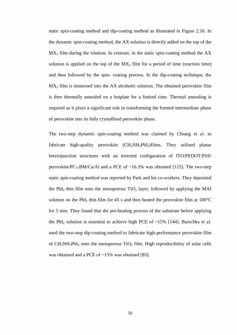
50
static spin-coating method and dip-coating method as illustrated in Figure 2.16. In
the dynamic spin-coating method, the AX solution is directly added on the top of the
MX2 film during the rotation. In contrast, in the static spin-coating method the AX
solution is applied on the top of the MX2 film for a period of time (reaction time)
and then followed by the spin- coating process. In the dip-coating technique, the
MX2 film is immersed into the AX alcoholic solution. The obtained perovskite film
is then thermally annealed on a hotplate for a limited time. Thermal annealing is
required as it plays a significant role in transforming the formed intermediate phase
of perovskite into its fully crystallised perovskite phase.
The two-step dynamic spin-coating method was claimed by Chiang et al. to
fabricate high-quality perovskite (CH3NH3PbI3)films. They utilised planar
heterojunction structures with an inverted configuration of ITO/PEDOT:PSS/
perovskite/PC71BM/Ca/Al and a PCE of ~16.3% was obtained [125]. The two-step
static spin-coating method was reported by Park and his co-workers. They deposited
the PbI2 thin film onto the mesoporous TiO2 layer, followed by applying the MAI
solution on the PbI2 thin film for 45 s and then heated the perovskite film at 100°C
for 5 min. They found that the pre-heating process of the substrate before applying
the PbI2 solution is essential to achieve high PCE of ~15% [144]. Burschka et al.
used the two-step dip-coating method to fabricate high-performance perovskite film
of CH3NH3PbI3 onto the mesoporous TiO2 film. High reproducibility of solar cells
was obtained and a PCE of ~15% was obtained [83].
51
Figure 2.16 Schematic diagram of the fabrication processes of the perovskite film by: (a) a two-step dynamic spin-coating method; (b) a two-step static spin-coating method; (c) two-step dip-coating method
52
2.4.5 Morphologies of halide perovskites
One of the main challenges in obtaining high-performance perovskite-based solar
cells is the control of the perovskite thin film morphology [145]. Physical
characteristics of halide perovskites including light absorption, charge carrier
transport, and diffusion length are highly reliant on the degree of crystallinity of the
perovskite thin film [134,146,147]. The crystallinity of the perovskite thin film
depends extremely on many factors such as deposition process, composition of
materials, perovskite structure, the used solvents and additives, annealing treatment
(thermal and solvent annealing), and humidity during preparation [47,134]. The
crystallisation process comprises two major processes; i.e. nucleation and crystal
growth [76].
The poor perovskite morphology arises from pinholes and incomplete surface
coverage which results in low-resistance shunting path and decreasing light
absorption. It is feasible to optimise morphologies of perovskite thin films by
selecting efficient techniques to manipulate nucleation and crystal growth in the
perovskite thin film. Several efforts have been exerted to optimise the morphologies
of the perovskite layer. The deposition method is one of the most significant factors
which impact on the morphology of the perovskite thin film. In the one-step
deposition method, the crystallisation process of perovskite crystals is very fast,
creating very poor surface morphology with pinholes in the film and discontinuous
film [118,134].
Different morphological control methods are presented in Table 2.1. Optimisation of
perovskite crystals in the films was achieved by Spiccia and co-workers using the
one-step deposition method. They deposited CH3NH3PbI3 thin film and then
followed by inducing a fast crystallisation process via exposing the perovskite film

53
to chlorobenzene. Smooth and homogenous thin films were produced with large
grain structure. A mean PCE of 13.9±0.7 was obtained in their solar cells [135]. It is
suggested that the morphology of the perovskite film fabricated by the spin-coating
technique could be influenced through two main factors; i.e. thermodynamic and
kinetic impact. Both thermodynamic and kinetic influences play their crucial
functions in the growth of perovskite thin film's morphologies [148]. The
thermodynamic effects are determined by fundamental characteristics of the
composition and concentration of the solutions which are utilised to fabricate the
perovskite thin film. These include, the proportion of (AX) to (MX2), degree of
interaction and solubility of the perovskite components. Kinetic factors on the other
hand are related to average solvent evaporation, post-treatment, and incorporation of
additives.
The two-step deposition method is an important technique which has its potential to
govern the crystallization in the perovskite film [83,149,150]. Park and co-workers
utilised the two-step spin-coating method to fabricate the CH3NH3PbI3 thin film in
TiO2-based planar heterojunction solar cells [151]. They identified that the cuboids
crystal in the perovskite exceptionally depended on the concentration of the
CH3NH3I solution. They optimised and controlled the cuboids crystals using a low
concentration of the CH3NH3I solution (0.038M), resulting in larger cuboids of
perovskite ( ~720 nm) and achieving a high PCE of ~17.01% for the solar cells
[151].
Furthermore, doping additives into the precursor’s solution is an alternative to
control the morphology of the perovskite film. Joen et al. have shown that the
morphology of the perovskite film can be controlled by adding a limited amount of
N-cyclohexyl-2-pyrrolidone (CHP) into DMF solvent. A uniform film with

54
complete coverage surfaces was obtained after the additive remained on the surface
during the formation of the perovskite film due to the high boiling point and low
vapour pressure of the N-cyclohexyl-2-pyrrolidone (CHP) [152]. In addition, Liang
et al. improved the crystallization process of the perovskite film by combining 1,8-
diiodooctane (DIO) into the precursor solution of perovskite, showing very smooth
surface and continuous thin film. The effect of additives in the precursor solution not
only enhances homogeneous nucleation but also changes the kinetic growth
mechanism of perovskite crystals [145].
Solvent annealing is another method to optimize the morphology of the perovskite
film when it's deposited in a saturated ambient environment containing solvent
vapour. It is a common technique which was widely used to optimize the
morphology of the photoactive polymer films in polymer-based photovoltaic
devices. Xiao et al. first used the solvent annealing method to optimize crystallinity
and grain size in the perovskite film by annealing the perovskite film in a saturated
environment of DMF vapour. The DMF vapour can assist the diffusion and
rearrangement of the precursor’s molecules and ions due to high degree of solubility
of PbI2 and CH3NH3I in DMF, giving the opportunity of perovskite crystals to grow
intensively [153].
Solvent engineering technique (SET) was used by Seok et al. in order to obtain
homogenous and very dense perovskite thin films. Two types of solvents, (γ-
butyrolactone and dimethylsulphoxide (DMSO) (7:3v/v)) were mixed with the
perovskite precursor solution to produce MAPb(I1−xBrx)3 perovskite film. Toluene
then dropped on the perovskite film during the spin-casting process of the perovskite
film, which led to the formation of a dense and uniform perovskite layer. [154].
High power conversion efficiency PCE of ~16.2% was achieved.
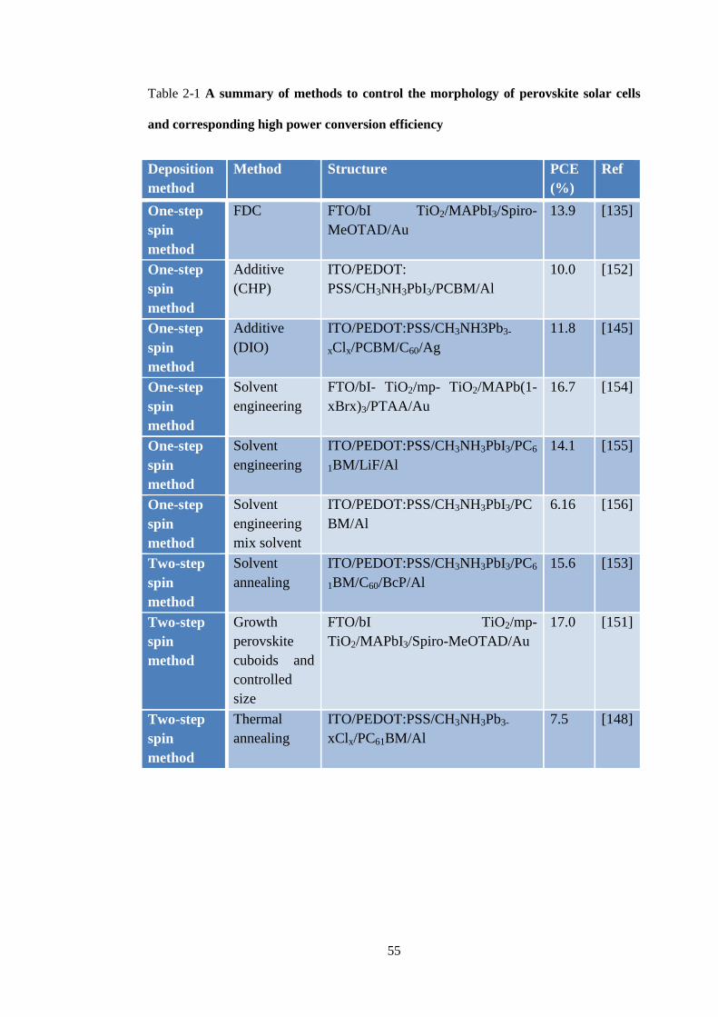
55
Table 2-1 A summary of methods to control the morphology of perovskite solar cells
and corresponding high power conversion efficiency
Deposition method
Method Structure PCE (%)
Ref
One-step spin method
FDC FTO/bI TiO2/MAPbI3/Spiro-MeOTAD/Au
13.9 [135]
One-step spin method
Additive (CHP)
ITO/PEDOT: PSS/CH3NH3PbI3/PCBM/Al
10.0 [152]
One-step spin method
Additive (DIO)
ITO/PEDOT:PSS/CH3NH3Pb3-
xClx/PCBM/C60/Ag 11.8 [145]
One-step spin method
Solvent engineering
FTO/bI- TiO2/mp- TiO2/MAPb(1-xBrx)3/PTAA/Au
16.7 [154]
One-step spin method
Solvent engineering
ITO/PEDOT:PSS/CH3NH3PbI3/PC6
1BM/LiF/Al 14.1 [155]
One-step spin method
Solvent engineering mix solvent
ITO/PEDOT:PSS/CH3NH3PbI3/PCBM/Al
6.16 [156]
Two-step spin method
Solvent annealing
ITO/PEDOT:PSS/CH3NH3PbI3/PC6
1BM/C60/BcP/Al 15.6 [153]
Two-step spin method
Growth perovskite cuboids and controlled size
FTO/bI TiO2/mp- TiO2/MAPbI3/Spiro-MeOTAD/Au
17.0 [151]
Two-step spin method
Thermal annealing
ITO/PEDOT:PSS/CH3NH3Pb3-
xClx/PC61BM/Al 7.5 [148]

56
2.4.6 Current limitations of halide perovskite-based solar cells
2.4.6.1 Stability of halide perovskite-based solar cells
The rapid degradation of organometal halide perovskite can be considered one of the
main challenges encountered by researchers in the perovskite photovoltaic
community. Poor long term stability is the major limitation for commercialisation of
halide perovskite-based solar cells. The degradation mechanism of halide
perovskite-based solar cells has not been fully investigated in the past five years;
most studies have been focused on enhancing the performance of the perovskite -
based solar cells [142]. The degradation mechanism for the perovskite-based PV
devices could be divided into three types; i.e. chemical, thermal, and environmental
degradation. The chemical degradation is caused by adjacent components such as
solvents, solutes, and additives which were used in numerous processing procedures
[76]. The thermal decomposition of halide perovskite is caused by exposing the
perovskite-based PV devices from low temperature to high temperature for a period
of time, which leads to decomposition of halide perovskite. The halide perovskite
film can convert gradually into the PbI2 film at increased temperature. It was
suggested that the thermal stability could be influenced by minor changes in the
synthetic processes and the precursors used [157]. The environmental degradation is
caused by exposing the unsealed perovskite-based PV devices to light, moisture and
oxygen. Due to their ionic nature, degradation of halide perovskite crystals shows a
high degree of sensitivity to light, moisture and oxygen [158,159]. High moisture
content in air can break the lattice structure between molecules and cause elements
to decompose [93]. Thereafter crystal structures of the perovskite film change to
metal halide. It was found that methylammonium lead iodide (CH3NH3PbI3) is more

57
sensitive to humidity compared with methylammonium lead bromide
(CH3NH3PbBr3) [160].
Noh et al. revealed that exposing methylammonium lead iodide to ~50% humidity
can result in decomposition, showing a colour change from dark brown to yellow.
However, the stability is remarkably enhanced after doping Br into perovskite
material to produce MAPb(I1-xBrx)3, where x=0.2 and 0.29 [161]. It was well known
that the perovskite-based liquid electrolyte structural PV devices have very poor
stability and a very short life span. The efficiency of the PV devices could degrade
in a few minutes because of high solubility of perovskite into the liquid electrolyte
[162]. The stability of the perovskite solar cells based on the liquid electrolyte was
greatly improved by changing the liquid electrolyte with a solid-state hole transport
layer [163].
Later, different techniques were used to enhance the stability of perovskite-based
solar cells as presented in Table 2.2. Burschka and his colleagues found that the
fabrication of perovskite solar cells by the two-step method retains more than 80%
of the performance of the encapsulated devices under illumination and increases the
life time of the sealed devices to ~500 h [83]. Kim et al. enhanced the environmental
stability of perovskite-based devices when they improved the morphology of the
perovskite layer using the blade-coating method. They demonstrated that the
morphology of the perovskite crystal thin films significantly improved after solvents
evaporated from the surface during the blade-coating process, resulting in the
formation of a large and compact crystalline domain in the perovskite layer [164].
There are other ways to enhance the stability of the perovskite-based solar cell
which adopts a proper electron and/or hole transport layer. It was found that
mesoporous TiO2 in the case of acting as the electron transport layer affects the

58
stability of the PV devices because TiO2 is unstable under UV illumination [93].
Using Al2O3 or ZnO nanorods instead of TiO2 elongate the life time of PV devices
[158,165]. Three different hole transport materials were explored by T. Park's group
[166] to investigate the impact of 20% humidity on the long-term stability over 1000
hours. They used Poly[2,5-bis(2-decyldodecyl)pyrrolo[3,4-c]pyrrole-1,4(2H,5H)-
dione-(E)-1,2-di(2,20-bithiophen-5-yl) ethene] (PDPPDBTE), P3HT, and Spiro-
MeOTAD as HTLs separately on top of TiO2/CH3NH3PbI3-based devices and
deduced that the semiconductive polymers HTLs maintained better performance of
the PV devices over the period of testing than Spiro-MeOTAD. The outstanding
stability of the polymer HTLs based perovskite devices was due to hydrophobicity
of the semiconductive polymers of PDPPDBTE and P3HT, which decreased the
infiltration of water into the perovskite surface [166]. Snaith et al. presented a novel
HTL of polymer-functionalized single-walled carbon nanotubes (SWNTs) for
replacement of PEDOT:PSS on top of CH3NH3Pb3-xClx thin film. The perovskite
devices showed unparalleled thermal stability and moisture resistance after the
devices were exposed to 80 °C in air for 96 h [167]. Snaith and co-workers replaced
the compositions of halide perovskites; for instance; replacing methylammonium
with formamidinium or iodide with bromide leads to increasing the stability of the
perovskite. FAPbI3 and CH3NH3BrX3 have better stability compared with MAPbI3
[168,169]. Mei et al. presented highly stable unsealed devices for 1008 h in the
normal environmental condition e.g., (AM1.5), light intensity at 100 mW cm-2 and
room temperature. They applied modified perovskite materials (5-AVA)x(MA)1-
xPbI3 with free hole transport materials and obtained a certified PCE of ~12.8%
after the perovskite layer was protected by a carbon layer which acted as a back
contact [170]. A low-temperature solution-processed material of PhNa-1T was used

59
instead of PEDOT:PSS as a hole transport layer, demonstrating that the stability of
PV devices was enhanced under ambient conditions of 25°C and 40% relative
humidity compared with devices using PEDOT:PSS. The device structure was
PEN/ITO/PhNa-1T /CH3NH3PbI3/PC61BM/Ag. It revealed higher resistance within a
replicate mechanical stress [171]. Zhao et al. claimed a novel configuration by
inserting a polymer as an insulated scaffold material, which led to enhancing the
stability to ~300 h in an ambient environment with 70% relative humidity. The
unsealed devices show a PCE of ~16%. This structure not only improved the
stability but also exhibited robust self-sealing or humidity-resistance, showing that
the perovskite devices could offer power conversion efficiency recovery after water
vapour attached on the surface and then evaporated [172].

60
Table 2-2 A summary of methods to enhance the stability of perovskite and corresponding high power conversion efficiency
Structure Method Device structure Life
time
PCE
(%)
Ref
TiO2 based
PHJ
Doping Br
into
CH3NH3PbI
3
FTO/Bl-TiO2/Ms TiO2/
CH3NHxPbBr3-x
_
12.3
[161]
TiO2 based
PHJ
Applying
HTMs
FTO/Bl-TiO2/Ms TiO2/
CH3NH3PbI3/ (HTMs)
1000
9.2
[166]
PCBM
based PHJ
Using blade
coating
technique
ITO/PEDOT:PSS/CH3N
H3PbI3/PCBM/C60/Ag
268 12.2
1
[164]
ZnO based
PHJ
Using ZnO as
ETL
FTO/ZnO/CH3NH3PbI3/s
piro-MeOTAD/Ag
500 5 [165]
TiO2 based
PHJ
Using Al2O3
as scaffold
FTO/BI-TiO2/Al 2O3
CH3NH3PbI3/spiro-
MeOTAD/Ag
18 4.6 [173]
TiO2 based
PHJ
Using HTL
PDPPDBTE
FTO/Bl-TiO2/MsTiO2/
CH3NH3PbI3/ (HTMs :
P3HT,PDPPDBTE and
spiro-MeOTAD)/Au
1000 9.2 [166]
TiO2 based
PHJ
Using
formamidiniu
m lead iodide
as
photoactive
layer
FTO/BI-
TiO2/FAPbI3/spiro-
MeOTAD/Au
_
14.2 [168]
PCBM
based PHJ
Using HTL
PhNa-1T
ITO/HTL(PhNa-1T)
/CH3NH3PbI3/PCBM/Ag
300 14.7 [171]

61
2.4.6.2 Toxicity of lead in halide perovskites
High PCEs of halide perovskite-based solar cells are currently only realised in
organic-inorganic hybrid lead halide perovskites. However, lead is very toxic and
not environmentally friendly [174]. Efforts have been made to search for an
alternative of lead-free halide perovskites. Hao et al firstly fabricated lead-free
hybrid halide perovskite solar cells based on tin iodide perovskite. They achieved
~5.7% using CH3NH3SnI3–xBrx as an absorber layer [42]. Then, Snaith and co-
workers reported lead free CH3NH3SnI3 perovskite solar cells and ~6.4% PCE was
reached [175]. However, Sn-based halide perovskite shows poor stability. The
decomposition starts just in 2 h after preparation and attains a total decomposition
after one day [42].

62
Materials Preparation and Characterisation Chapter 3 -
3.1 Introduction
In this chapter, preparation of photoactive materials, hole and electron transport
materials, and bottom and top electrodes for fabrication of the solar cells in this
thesis will be explained. This will include details of experimental techniques used to
characterise the photoactive polymer, halide perovskite, and photoactive polymer-
perovskite composite materials.
In this thesis, three different configurations and photoactive materials were
employed. The first photoactive layer is P3HT that is blended with PCBM in the
bulk heterojunction-based solar cells. The second photoactive layer is halide
perovskite of methylammonium lead iodide in PCBM-based planar heterojunction
solar cells. The third photoactive layer is a composite of methylammonium lead
iodide perovskite and photoactive polymer PTB7 in PCBM-based planar
heterojunction solar cells. Typically, the active layer is sandwiched between two
electrodes in all three solar cells architectures. The first electrode should be at least
semi-transparent, which allows sunlight passing through to reach the photoactive
layer.
Usually, indium doped tin oxide (ITO) or fluorine doped tin oxide (FTO) are used
and the opposite electrode is typically a thin film of metal including aluminium,
silver, gold, etc.

63
3.2 Materials preparation and properties
3.2.1 Photoactive materials for polymer solar cells
The bulk heterojunction structure was used to fabricate solution-processed polymer
solar cells. The photoactive layer consists of a blend of the conjugated polymer poly
(3-hexylthiophene) (P3HT) as the electron donor and a small molecule material
(fullerene derivatives) of PCBM semiconductor as the electron acceptor. The P3HT
has been broadly used in a variety of applications including solar cells, OLEDs and
transistors [176]. The mixture of P3HT:PCBM has attracted a significant attention in
the last decade [177]. The performance of polymer solar cells relies on the quality of
the crystallinity and the regioregularity of the polymer [178]. Amongst various
conjugated polymers, P3HT is notably recognised to exhibit a high degree of
crystallinity and displays comparatively excellent charge transport properties [179].
In turn, the crystallinity of the photoactive layer is linked with the regioregularity of
the conjugated polymer. In many cases, P3HT is observed to have more than 90%
regioregularity, which increases the level of crystallinity of the active layer.
Some other factors such as the weight ratio between the donor and the acceptor, the
type of solvents used, the thermal annealing treatment, and the thickness of the
photoactive layer have significant impact on the performance of OPV devices [180].
Among the fullerene additives, PCBM is considered as one of the most attractive
variants, which has been widely used as the electron acceptor. This is due to its
solubility in chlorobenzene, which subsequently enables the use of solution-
processed method to deposit the active layer.

64
Figure 3.1 The energy level of P3HT:PCBM [177]
Furthermore, the blending of P3HT:PCBM is shown to absorb photons in the
wavelength range of 380-670 nm, implying that the exciton in the active layer is
generated by the absorption of photons with energies between 2.0 and 3.3 eV [177].
Figure 3.1 illustrates the energy levels of P3HT:PCBM. In order to achieve an
efficient charge separation in the solar cells, the HOMO and LUMO of the donor
must be 0.2-0.3 eV larger than the HOMO and LUMO of the acceptor [177]. In the
case of a smaller or larger offset, it may be difficult to acquire an effective charge
separation as most of the energy will dissipate [177]. However, when the energy of
photons is higher than 2.0 eV, a small proportion will be absorbed by the
photoactive layer of P3HT:PCBM and 70% of the remaining energy of photons will
be wasted in heat [43]. Therefore, in order to minimise the loss of energy as much as

65
possible, doping the donor and acceptor components is crucial to the assembly
process.
3.2.1.1 Preparation of polymer photoactive layers
P3HT used in the current research was purchased from Merck (Lisico) and has a
regioregularity of more than 94%. PCBM was purchased from Solenne BV and has
a purity of 99.5%. 30 mg concentration of the blend with an equal molar ratio of
P3HT to PCBM was dissolved in 1 mL of chlorobenzene and stirred overnight on a
hotplate. The mixture was then filtered by the 0.45 m PTFE filter to remove large
particles.
3.2.2 Photoactive materials of halide perovskites for solar cells
Methylammonium halide perovskite (MAPbI3) was selected as the photoactive layer
for the PCBM-based planar heterojunction solar cells. This type of material has
attracted great deal of attention due to some unique characteristics that distinguish it
from other solar cell materials. It has a narrow band gap of ~1.55 eV, outstanding
performance of high efficiency, and ability to harvest a high number of the incident
photons from the visible range up to 800 nm [85]. The methylammonium halide
perovskite consists of two main materials: lead iodide (PbI2) and methylammonium
iodide (MAI). The PbI2 powder was purchased from Sigma-Aldrich while the MAI
salt was synthesised in our lab according to the procedure described later in this
chapter.
MAPbI3 thin films were fabricated via two deposition methods: i) (OSSCM), and ii)
(TSSCM). In OSSCM, PbI2 was firstly mixed with MAI using appropriate solvents
such as DMF or dimethyl sulfoxide (DMSO). In TSSCM, PbI2 in DMF solvent was
firstly applied on top of HTMs, and then MAI in the IPA solvent was applied onto

66
the pre-coated PbI2 film, followed by thermal annealing at 100°C for a period of
time to complete the reaction and thus the perovskite thin film was produced. Figure
3.2 shows the energy level of the perovskite structure. MAPbI3 acts as a donor
material which has a HOMO at -5.43 eV and a LUMO at -3.93 eV, respectively.
PCBM was used as an acceptor material in the planar heterojunction PV structures
with a HOMO at -6.0 eV and LUMO at -4.2 eV.
Figure 3.2 Energy level of perovskite structure [181]
3.2.3 Photoactive polymer-perovskite composite for solar cells
A novel composite photoactive layer is used to fabricate organic-inorganic hybrid
solar cells. The composite consists of methylammonium halide perovskite MAPbI3
and PTB7 polymer. Figure 3.3 shows the energy levels of the photoactive polymer-
perovskite composites. Similar energy levels were used for the MAPbI3 and PCBM,
while PTB7 polymer is shown to act as a donor in addition to MAPbI3 and has a
HOMO at -5.3 eV and LUMO at -3.5 eV respectively.

67
Figure 3.3 Energy levels of the photoactive polymer-perovskite composite
3.2.3.1 Preparation of perovskite materials
MAI was synthesised in the ambient atmosphere at room temperature via the
chemical reaction of 27 ml methylamine solution (CH3NH2, 40 wt.% in methanol,
TCI) with 30 ml of hydriodic acid (HI 57 wt.% in water, Aldrich) in a round
bottomed flask. This process was carried out at 0°C in an ice bath for two hours. The
methylamine solution was added first into the round-bottomed flask and then
hydroiodic acid (HI) was dropwise added in during stirring. White precipitate of
MAI was collected after the mixture in the solution was transformed into a rotary
evaporator and heated at 50°C for one hour. The white precipitate was washed three
times with diethyl ether and finally dried in vacuum for 24 h.
The PbI2 solution was prepared by dissolving 1 mole PbI2 in 1 ml DMF solvent and
then 20 l of DIO was added into the solution to promote the dissolution of PbI2.

68
The PbI2 solution became clear after continuous stirring at 70°C overnight as shown
in Figure 3.4.
Figure 3.4 PbI2 solution; left) before adding DIO, right) after adding DIO
3.2.4 Electron transport layer
Electron transport materials play a critical role in the polymer and perovskite solar
cells allowing for the transport of electrons and blocking of holes. The ohmic
contact aligning between the LUMO of the donor material and the electron
collecting electrode is an essential factor which impacts on the transport and
collection of the electrons. Furthermore, the high electron affinity is required to
facilitate the pathway of electrons proficiently and to stop holes transport in the
photovoltaic devices [52,182]
In the polymer PV devices, ZnO thin film was chosen as the electron transport
material due to numerous beneficial features, such as high transparency, high
electron mobility, and wide bandgap. Moreover, the ZnO film can be fabricated by

69
the sol-gel solution method, which has the potential of providing a highly wetting
surface and good adhesion with the photoactive layer of the polymer [183].
In the pure perovskite and photoactive polymer-perovskite composite devices,
PCBM was used as the electron transport material. PCBM is a prominent competitor
as an alternative to TiO2 in the perovskite's solar cells due to its simple fabrication
process, enabling it to be deposited in a normal environment at low temperatures
[93]. Furthermore, PCBM has a high electron affinity and high degree of solubility
in chlorobenzene, dichlorobenzene, and chloroform, which allows the film to be
deposited by the solution-based processing techniques of the spin- or dip- coating
method.
3.2.4.1 Preparation of ZnO and PCBM solutions
The sol-gel method was used to prepare the ZnO colloid solution. 0.1 M of the
precursor zinc acetate dihydrate was dissolved in 2-methoxyethanol. Ethanolamine
was then added into the solution in order to adjust the pH value to less than 7. The
molar ratio of Zinc acetate to ethanolamine is at 1:1. The solution was then stirred
for 1 hour in air. The fullerene derivative [6,6]-phenyl-C61-butyric acid methyl ester
(PCBM) is broadly utilised as an acceptor material in solar cells by either blending
PCBM with P3HT in the polymer solar cells or depositing as a separate thin film on
top of the perovskite film in the planar heterojunction perovskite solar cells. Two
diffrenet concentrations of PCBM (30 mg and 40 mg) were dissolved in 1 ml
chlorobenzene and stirred on a hotplate at 70°C for 2 hours, and then the solution
was filtered using 0.45 µm PTFE filter to obtain very high purity PCBM solution.

70
3.2.5 Selection of the cathode buffer layer
Bathocuproine (BCP) was selected as the cathode buffer layer. The main benefit of
inserting the cathode buffer layer between the acceptor material and the cathode is to
enhance the extraction and collection of the negative charge carriers [112].
Furthermore, (BCP) plays a key role in providing protection to the photoactive layer
and contributing to obtain ohmic contact with the top electrode [74]. Theoretically,
the low work function electrode is required to extract the negative charge carriers in
the inverted structure. However, high work function electrodes such as Au can also
effectively provide electrons extraction layer in many cases [112].
3.2.5.1 Preparation of the cathode buffer layer (BCP)
To prepare a solution-processed bathocuproine buffer layer, 2 mg (BCP) was
dissolved into 1 mL methanol and then sonicated for 10 minutes. The solution was
then stirred for 30 min on a hot plate at 40°C followed by passing the solution
through the 0.45 µm PTFE filter to obtain a pure BCP solution.
3.2.6 Hole transport laye
Different HTMs have been used in the polymer and perovskite solar cells such as
MoO3, V2O5, PEDOT:PSS and spiro-MeOTAD. In the perovskite-based solar cells,
spiro-MeOTAD is a common material which has been widely utilised as the hole
transport material. However, the complicated processes for the synthesis of the
material leads to a very high commercial cost [117].
The selected hole transport material in this thesis is PEDOT:PSS for all
configurations due to its highly valued advantages of low-cost, ease of applying as
thin film, superb transparency, chemical stability and high hole conductivity [76].
PEDOT:PSS was employed between the active layer and the opposite electrode. The

71
essential factor of the hole transport layer (PEDOT:PSS) is that the material’s
energy levels are suitable to facilitate the holes transport and blocks the electrons
transport. An efficient hole transport layer should produce an ohmic contact with the
electrode and match the Fermi level of the donor to enhance the transport of holes
and effectively block the passage of electrons.
In this thesis, PEDOT:PSS was applied on top of the blend of P3HT:PCBM and at
the bottom of the perovskite layer or the composite perovskite/PTB7 layer,
respectively. The PEDOT:PSS can be uniformly deposited on the ITO-coated glass
substrate. However, it is hard to obtain a uniform thin film of PEDOT:PSS on the
top of the P3HT:PCBM film due to hydrophobic feature of the blend film. Different
treatments were utilised to overcome this issue in order to deposit uniform film;
these are i) adding a surfactant [184], and ii) using co-solvents [185].
3.2.6.1 Preparation of PEDOT:PSS
Poly(3,4-ethylenedioxythiophene): poly(styrene sulfonate) (PEDOT:PSS) (1.3-1.7
wt% in water) was purchased from Ossila which has a work function of ~ 5.1 e V.
The PEDOT:PSS solution was filtered using 0.45 m PVDF filter before use in
order to remove any large-sized particles. Different surfactants (e.g., Triton or Zony)
were added to the PEDOT:PSS solution at 1% X-100 in volume to enhance the
wettability of the hydrophobic blend film in the photoactive layer [186]. Dip- and
spin- coating methods were respectively utilised to fabricate the thin films of
PEDOT:PSS, followed by the thermal annealing at 140°C for 15 min.

72
3.2.7 Electrode materials
In this thesis, all fabricated devices were applied onto glass substrates coated with
indium tin oxide (ITO) thin film. Indium tin oxide (ITO) is one of the most broadly
used materials as an anode or cathode [12], with the work function of ITO at - 4.8
eV. Au (with the work function of -5.1 eV) is used as the top electrode in this thesis.
The PVD sputtering coating technique was used to deposit the thin film of Au on the
PV cells.
3.2.8 Cleaning procedure
Indium-tin-oxide (ITO) coated glasses were cut into small slides of 2 × 2.5 cm2. The
etching process was used to pattern the ITO-coated glasses by applying a mixture of
Zn powder and hydrochloric acid (HCl). Cleaning the substrates before fabricating
solar cells is an essential step to remove any sorts of impurities on the substrates.
The patterned ITO substrates were firstly cleaned by the soap solution and washed
by deionized (DI) water. Then, the substrates were sonicated separately in acetone
and isopropanol for 10 min, followed by washing the substrates by DI water.
Finally, the substrates were blown dry using N2. The same procedure was applied to
clean any other glass substrates for materials analysis using SEM, AFM, UV-Vis
FTIR and PL.
3.3 Characterisation methods
3.3.1 Characterisation of the PV devices
J-V characterisation was performed under the simulated AM 1.5G irradiation (100
mW /cm2) using Keithley 2401 sourcemeter under ambient environment. A Schott
KG5 colour-filtered Si diode (Hamamatsu S1133) was utilised to calibrate light
intensity of the solar light simulator before J-V measurements were carried out. An

73
aperture of aluminium mask was applied on the PV devices to obtain an active area
of 0.04 cm² and to prevent any contribution from externally fallen light on the
devices. External quantum efficiency (EQE) spectra were measured by a home-built
spectral response measurement set-up. X-ray diffraction (XRD) patterns were
obtained using Philips X’PERT MPD with Cu-K� X-ray source of wavelength 1.54
Å and with operational parameters of 40 kV tube voltage and 40 mA tube current.
Scanning electron microscopy (SEM) was used to investigate the morphologies of
the perovskite thin films using Nova Nano Microscopic instrument. Reflectance
FTIR spectra were recorded in the frequency range of 800-4000 cm-1 using Nexus
FTIR instruments (Thermo Nicolet Corp, USA) with ATR-FTIR spectrometer. FTIR
samples were prepared on the Au-coated glass slides. Atomic Force Microscopy
(AFM) images were obtained by Bruker multimode. Steady-state
Photoluminescence (PL) spectra were recorded by the Varian cary eclipse
fluorescence spectrophotometer upon excitation 400 and 620 nm, separately.
3.3.2 Current-Voltage (I-V) Characterization
One of the most important methods to determine the performance of PV devices is
the I-V characterization. The measurements were carried out by employing source
meter and a solar simulator. I-V curves of the investigated devices will be drawn as
a result of applying different values of voltage within a specified range and
recording the corresponding current values. Tests are conducted either in the dark or
under illumination in order to derive the PV device parameters, including Voc, Isc,
FF, serious resistance, shunt resistant, and PCE as shown in Figure 3.5.
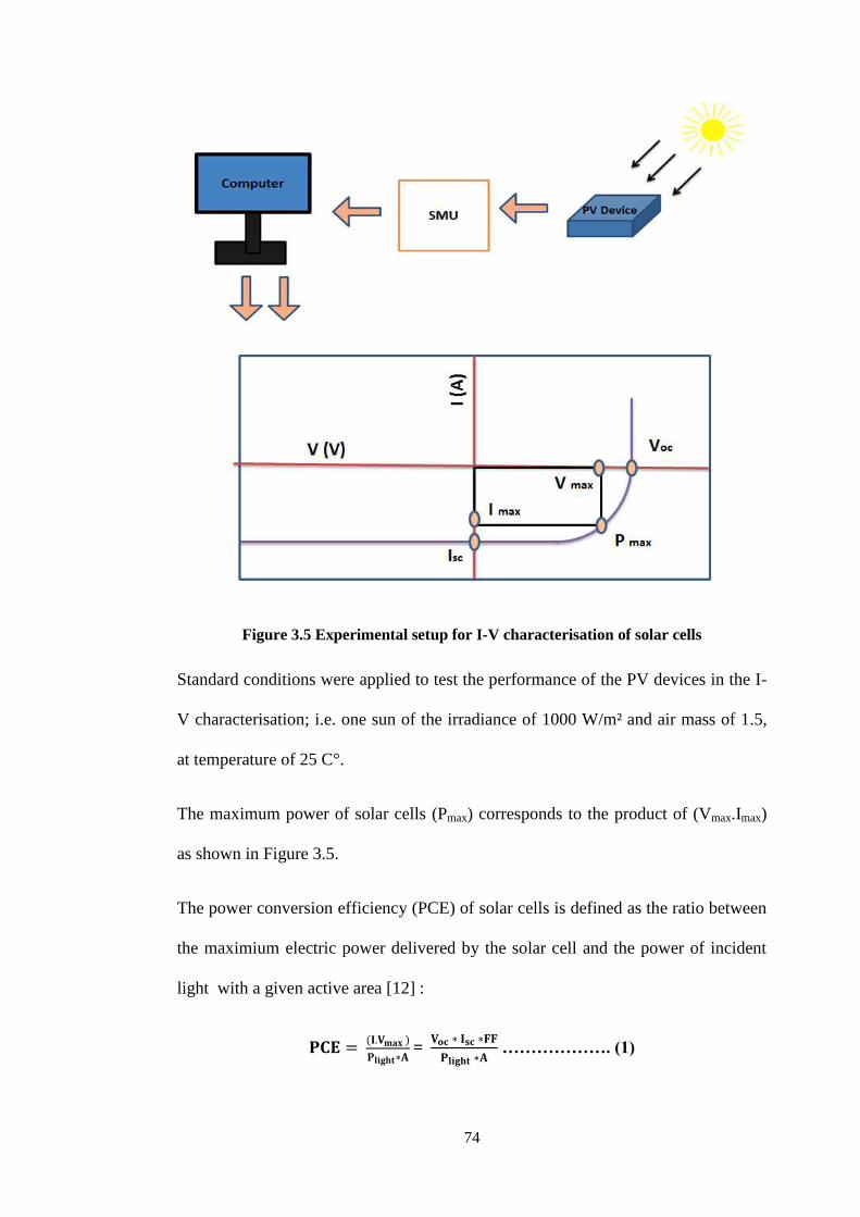
74
Figure 3.5 Experimental setup for I-V characterisation of solar cells
Standard conditions were applied to test the performance of the PV devices in the I-
V characterisation; i.e. one sun of the irradiance of 1000 W/m² and air mass of 1.5,
at temperature of 25 C°.
The maximum power of solar cells (Pmax) corresponds to the product of (Vmax.Imax)
as shown in Figure 3.5.
The power conversion efficiency (PCE) of solar cells is defined as the ratio between
the maximium electric power delivered by the solar cell and the power of incident
light with a given active area [12] :
�� = .� �� � ∗� = � � ∗ � ∗� ∗� ……………….(1)

75
where fill factor (FF) is defined as
FF= .� �� � �∗ � … ….………………..(2)
where Voc is the open circuit voltage, Isc is the short circuit current, and Plight is the
intensity of incident light.
3.3.3 Atomic Force Microscopy (AFM)
AFM was used to identify the surface topography of the materials with high
resolution using tapping mode. In this type of sample scanning, a sharp probe is
installed on the cantilever of the tip taps over the surface of the sample during
scanning. The cantilever tip is stimulated to oscillate near the resonance frequency
(~300 kHz). Different distances between the tip and the surface of the sample
recorded changes in the surface topography as shown in Figure 3.6.
Figure 3.6 Schematic diagram of the atomic force microscopy (AFM)

76
Analytic software was then used to analyse those variations which are measured by
the photodetector. Several types of operation modes have been used in AFM
including the contact mode where the probe contacts the surface constantly and the
tapping mode where the probe intermittently taps the surface or the probe hovers
over the surface. The tapping mode is widely used in AFM characterization due to
its high resolution and sample protection (friction causes damage in other modes).
3.3.4 Scanning Electron Microscope (SEM)
The scanning electron microscope has been used to form a significantly magnified
image with great visibility and high resolution of the surface morphology of
specimens. In this instrument, as shown in Figure 3.7, the electron gun located at the
top of the SEM instrument produces a beam of electrons by heating the metallic
filament of tungsten. This beam of electrons vertically moves down through
electromagnetic lenses. When the beam hits the sample, electrons and X-rays are
dispersed and ejected from the sample and are then collected by the detector. The
detector converts these electrons into signals which are sent to the computer and
finally the SEM image is obtained. SEM operates inside a vacuum chamber using
high-energy electron source (2-25 KV). The samples were coated by a thin film of
Au to eliminate surface charging.

77
Figure 3.7 Schematic diagram of the principle of SEM
3.3.5 UV-Vis Spectroscopy
UV-Vis spectroscopy is one of the oldest techniques that contribute to identify the
organic structure, orientation and ordering structure of molecules. Commonly,
organic molecules and halide perovskite absorb light in the spectral region between
~ 300-800 nm. The photons energy might be absorbed by molecules in specific units
or quanta units, that is compatible with the energy difference between HOMO and
LUMO levels. Light absorption usually happens when the light radiation falls on the
active layer with sufficient energy to cause electron transition from the bonding σ, π
and the nonbonding (n) orbitals to the antibonding σ* and π* orbitals respectively as
shown in Figure 3.8 [187].

78
Figure 3.8 Schematic diagram of electronic transition level
There is a widely used formula regarding absorption and transmittance (T) which is
the Beer-Lambert's law. It depicts that the absorption of incident light when passes
through a medium is proportional to the thickness of the medium. It's intensity
decreased exponentially in the formula [187,188]:
� = � −�� … … … … … … … … … … … … …(3)
or
� �⁄ = �� …………………………….(4)
where �� is the intensity of incident light, I is the intensity of light after passing
through the sample at a thickness x, � is a constant (absorption coefficient) as shown
in Figure 3.9.

79
Figure 3.9 Graphical illustration of the Lambert-Beer law
When using common logarithms (base10), equation (3) will become:
� = � × − � ………………………….(5)
or
log � �⁄ = kx …………………………..(6)
where k= �/2.303 is the extinction coefficient. Beer's law depicts that the absorption
is proportional to the concentration of the medium, where k = ƐC, Ɛ is the extinction
coefficient for unit concentration (L mol-1 cm-1), c is molar concentration (mol /L),
and x is path length of the sample (cm). By combining Lambert's and Beer's law, the
new formula is
� = � � �⁄ = � �…………………………..(7)
The logarithm term ( � �⁄ is known as absorbance (A), which is plotted in the UV-
spectrum versus to the wavelength ( ).

80
The concept of the absorption method can be summarised by shedding
monochromatic light through the surface of the film and collecting the
corresponding data of the transmitted light. Consequently, we can calculate the
absorption of light at each wavelength. The working principle of UV-Vis spectrum
is shown in Figure 3.10
Figure 3.10 The principle of UV-Vis spectroscopy
3.3.6 Photoluminescence (PL)
Photoluminescence spectroscopy is a contactless and non-destructive technique for
the study of the electronic structure of materials. The photo-excitation process
caused by absorption of incident photons by the electrons within the sample, which
results in exciting the electrons to higher electronic state and then the surplus energy
will release by emission of light or luminescence [189].

81
Figure 3.11 Schematic diagram of the photoluminescence setup
The phenomenon of photo-excitation is identified as photoluminescence, and it is
schematically described in Figure 3.11. This technique is usually utilised to
determine the performance of the excited charges splitting up at the interface among
the donor and acceptor materials [190]. In the case of interface between perovskite
and PCBM, once the donor material absorbs photons, it will release lights via the
photoluminescence procedure. When the acceptor materials applied on top or mixed
with the donor, a quenching of photoluminescence occurs indicating that many
excitons are separated to free charges. As the separation ratio of free charges
increases, quenching of photoluminescence will increase. Further, quenching of
photoluminescence will take place as a result of applying the HTL and ETL to the
photoactive layer [106].

82
3.3.7 X- Ray Diffraction (XRD)
One of the most familiar techniques for the characterisation of crystallinity of
materials is the non-destructive XRD technique. Figure 3.12 shows the principle of
X-ray diffraction measurements. A diffraction pattern which is produced by
diffraction from different planes contains information about internal structures of the
materials, degree of crystal orientations, phases and average grain sizes [191]. XRD
peaks have been produced after overlapping of a monochromatic beam of x-rays
dispersed at a specific angle for each lattice plane of the sample [192]. The peak
intensities are identified through distribution of atoms inside the lattice planes. The
number of peaks depends on the structure of the material. For instance, single crystal
(one orientation in structures) will produce only one peak in the diffraction pattern
while the polycrystalline samples which contain many differently oriented
crystallites will produce many peaks [193].
Figure 3.12 Schematic diagram of the X-ray diffraction measurement system

83
Figure 3.13 schematically demonstrates the Bragg’s law of diffraction. Bragg’s law
is typically used to determine the required conditions for diffraction, as described by
the following equation [194]:
� = Ɵ …………………….(7)
where, is an integer (1, 2, 3), � is the wavelength of the X-rays, Ɵ is the angle
between the incident rays and the surface of the crystal, and is the spacing
between layers of atoms.
Figure 3.13 Schematic diagramofBrag’s law of diffraction
3.3.8 Fourier transform infrared spectroscopy (FTIR)
Infrared spectroscopy is a beneficial characterisation method which is widely used
to identify the compound structure of organic or inorganic materials. The process of
infrared spectroscopy is similar to that for UV-vis spectroscopy in the absorption
measurement except it works in the infrared region as illustrated in Figure 3.14 [52].
When the sample’s irradiated by the infrared light, the absorbed spectrum can be

84
analysed by linking a specific characteristic frequency to the functional group and
therefore determining the composition of the sample [52].
The infrared spectroscopy measurements can take place using absorption, emission,
and reflection. Infrared spectroscopy is a technique which depends on the vibrations
of the molecules as its energy is not adequate to induce electron transitions from the
valence band to the conduction band. Alternatively, infrared photons excite
vibrational and rotational motion in the molecules [195]. Typically, an infrared
spectrum is attained by passing the infra radiation through the substrate and then
identifying the portion of the incident radiation which is absorbed at a specific
energy. The energy at any position of peak in the absorption spectrum refers to the
frequency of the vibration of an element of the sample molecule [195].
Figure 3.14 Schematic diagram of the Fourier transform infrared spectroscopy
3.3.9 External quantum efficiency
The external quantum efficiency is the proportion of charge carriers gathered by the
solar cell to the quantity of photons of a given energy incident on the solar cell.
Consequently, both the absorption of photons and the collection of free charges play
an important role in determining the external quantum efficiency. Electron-hole
pairs which are created as a result of absorbing incident photons by the PV active
layer. This pair should be separated to free charges and then collected by the
corresponding electrodes to reduce the possibility of recombination. Charge
recombination will cause reduction in the external quantum efficiency � [177]:

85
� = ƞ�. ƞ ��� . ƞ ���. ƞ ………………… (7)
where, ƞ� is the efficiency of the incident photons absorption, ƞ ��� is the efficiency
of the photo-induced exciton diffusion at heterojunction, ƞ ��� is the efficiency of
the exciton dissociation at the heterojunction and ƞ is the efficiency of charge
carrier transport and collection at the electrodes.
In addition, the internal quantum efficiency (IQE) is defined as the proportion of
charge carriers gathered by the solar cell to the quantity of photons of a given energy
incident on the solar cell and absorbed by the cell. The transmitted and reflected
lights are out of consideration to calculate the IQE [196]
�� = − − …………………………….(8)
where, R is reflectance and T is the transmittance.

86
Fabrication of P3HT:PCBM heterojunction solar cells Chapter 4 -by the dip-coating method
4.1 Introduction
The solution-processable photovoltaic devices (SPPDs) mainly, including dye-sensitized
TiO2 [197], quantum-dot nanoparticles [14], organic semiconducting polymers [198], and
very recently perovskites [16] represent great opportunities and advantages of simple
fabrication, cost effectiveness, devices on flexible substrates, and large area devices by the
roll to roll (R2R) technology [17–19] or other simple solution manufacturing methods [199].
The solution-processed methods may be classified as spin-coating, spray-coating, dip-
coating, doctor-blading, screen (or ink-jet) printing methods, etc. [73,200]. Spin coating is
one of the most efficacious techniques and has been widely used in laboratories for
fabrication of SPPDs due to its advantages of ease of use and high-degree of regularity for
film forming. In the fabrication of SPPDs, spin coating is the most commonly used method
as reported in the published literature. Nevertheless, there is a significant limitation to the
spin-coating method that is it is only suitable for small-scale fabrication or small area
devices, and is not compatible with the commercial applications for large-scale devices.
Other methods have their advantages and drawbacks [18].
The spray-coating method needs precise control on the nozzle and the liquid droplets may
splash onto the previously coated areas affecting the properties of the photovoltaic (PV)
devices [69].
The doctor-blading or the printing methods can easily realise the R2R manufacturing of PV
devices. However, their disadvantages could include complicated chemistry of ink
formulations and contact effects when the latter layer is applied on the previously formed
film [69].

87
The dip coating method has its own features and potential to be used as a promising
alternative for fabricating large area SPPDs on industrial scale. Historically, the dip-coating
process is a very old technology of producing sol–gel thin films, which was invented by
Jenaer Glaswerk Schott & Gen. in 1939 for silica films [72]. A schematic diagram is shown
in Figure 4.1 for the dip-coating process. The substrate is pulled vertically from the coating
bath at a constant speed (��). The entrained liquid by the moving substrate splits into two at
the free surface (point S in Figure 4.1) in a viscous boundary layer, returning the outer layer
to the bath. When the upward moving flux is balanced above the stagnation point S due to
evaporation of the solvents, a continuing and position-stable film is formed with respect to
the coating bath surface.
Figure 4.1 Schematic diagram of the dip-coating technology
Within the drying process, the colloids are progressively concentrated by evaporation,
leading to aggregation, gelation, and final drying to form a type of a dry gel or xerogel film.
When the substrates’ speed (��) and liquid viscosity (�) are low, e.g. in the case of the sol–
gel coating,

88
the thickness of the wet film can be written as:
� = [0.94 � × �� ⁄ ]/[� 6⁄ × � ⁄ ]…………………… (1)
Where � is the liquid–vapour surface tension, is the liquid density and � is the
acceleration of gravity [201]. Dip-coating process is a simple high productivity technique
with a high accuracy to deposit a uniform film on a large-scale area. Nowadays, many
commercial optical functional sol–gel thin films on glass have been manufactured by the
dip-coating method with a large area of several square metres. Moreover, the dip-coating
method owns the advantages of significantly reducing the amount of wasted materials
during the processing and the potential capability of depositing two PV devices at the same
time. Polymer photovoltaic devices (PPVs) have attracted considerable interests in the last
decade due to their potential advantages of the solution-processable manufacturing. Power
conversion efficiency (PCE) has increased after bulk heterojunction (BHJ) structures were
introduced in the devices [31], where the donor (organic polymers) blends together with the
accepter (fullerene derivatives) in a thin combined film placed between the electron
transport layer (ETL) and the hole transport layer (HTL) that are connected to the electrode
layers separately. In the past few years, 8% PCE has been obtained in a single BHJ device
using the new low band gap material [202–205]. Very recently, the PCE achieve a giant leap
up to 11.5% for the single BHJ [21].
Although these significant achievements have pushed the technology of PPVs further
towards the application of commercial products, there are still huge challenges to be
overcome with much effort including large area high-PCE devices and long-term stability of
the devices.
Dabirian et al. investigated the properties of the dip-coated PCBM [206]. Xue et al.
produced bundles of P3HT nanorods by using the dip-coating method [207]. Hu et al. has
published a study to deposit the active layer of PPV devices in the conventionally structural
devices [208].

89
In this chapter, we report the deposition of all layers except the electrodes in the inverted
PPVs by dip-coating technology. The blend of the active layer based on the chlorobenzene-
dispersed P3HT:PCBM has been modified and transformed it into a sol–gel-like solution by
adding petroleum ether. Figure 4.2 shows a gel of the P3HT:PCBM blend with a high
concentration of petroleum ether after stored in a closed bottle in the glovebox for two days.
The blend can also form a gel much faster with the evaporation of chlorobenzene than that it
is stored in the closed environment, which is compatible with the use of the dip-coating
process in order to fabricate a uniform active layer for PPV devices. The dip-coating method
has also been used to produce the ETL and HTL layers. Efficient devices with a PCE around
3.4% were obtained. This exploration demonstrates that the dip-coating method has its own
potential and advantages to be used as an industrial scale method for fabrication of all layers
of SPPDs.
Figure 4.2 Photos of the P3HT:PCBM blend: left) a gel formed from the modified blend; right) the liquid blend of the unmodified P3HT: PCBM in chlorobenzene
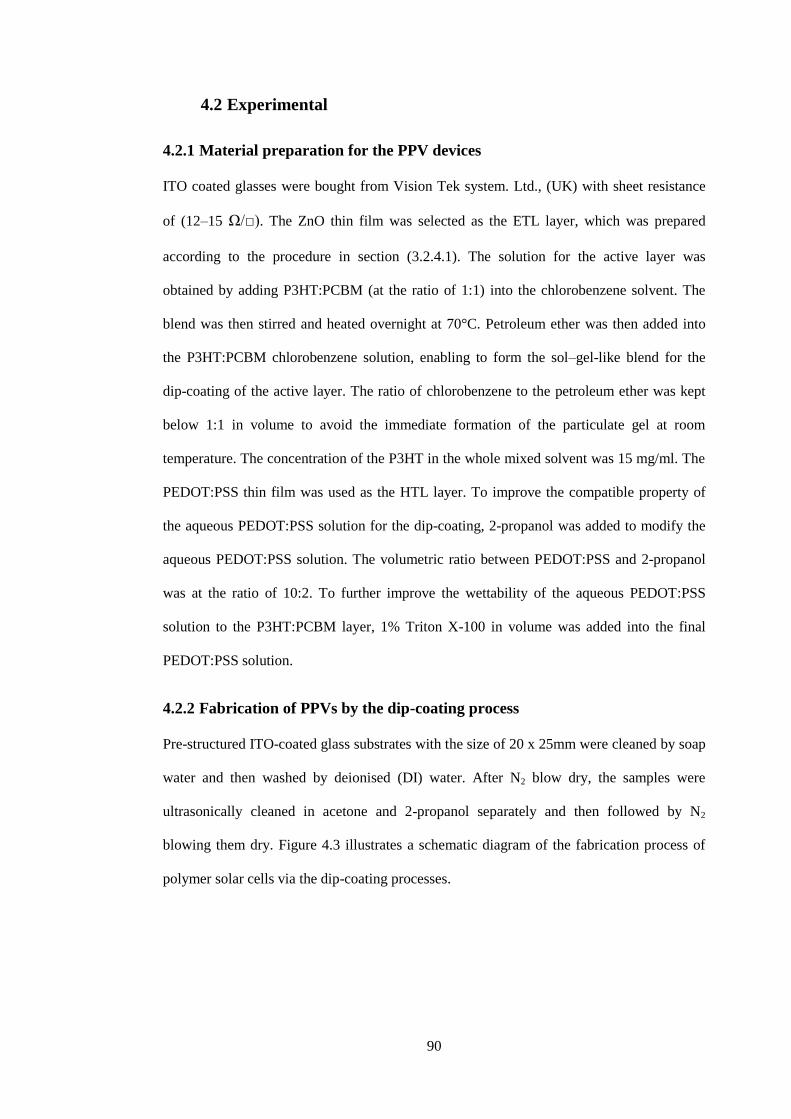
90
4.2 Experimental
4.2.1 Material preparation for the PPV devices
ITO coated glasses were bought from Vision Tek system. Ltd., (UK) with sheet resistance
of (12–15 Ω/□). The ZnO thin film was selected as the ETL layer, which was prepared
according to the procedure in section (3.2.4.1). The solution for the active layer was
obtained by adding P3HT:PCBM (at the ratio of 1:1) into the chlorobenzene solvent. The
blend was then stirred and heated overnight at 70°C. Petroleum ether was then added into
the P3HT:PCBM chlorobenzene solution, enabling to form the sol–gel-like blend for the
dip-coating of the active layer. The ratio of chlorobenzene to the petroleum ether was kept
below 1:1 in volume to avoid the immediate formation of the particulate gel at room
temperature. The concentration of the P3HT in the whole mixed solvent was 15 mg/ml. The
PEDOT:PSS thin film was used as the HTL layer. To improve the compatible property of
the aqueous PEDOT:PSS solution for the dip-coating, 2-propanol was added to modify the
aqueous PEDOT:PSS solution. The volumetric ratio between PEDOT:PSS and 2-propanol
was at the ratio of 10:2. To further improve the wettability of the aqueous PEDOT:PSS
solution to the P3HT:PCBM layer, 1% Triton X-100 in volume was added into the final
PEDOT:PSS solution.
4.2.2 Fabrication of PPVs by the dip-coating process
Pre-structured ITO-coated glass substrates with the size of 20 x 25mm were cleaned by soap
water and then washed by deionised (DI) water. After N2 blow dry, the samples were
ultrasonically cleaned in acetone and 2-propanol separately and then followed by N2
blowing them dry. Figure 4.3 illustrates a schematic diagram of the fabrication process of
polymer solar cells via the dip-coating processes.

91
Figure 4.3 A schematic diagram of the fabrication processes for P3HT:PCBM solar cells via the dip-coating method
The cleaned ITO coated slides with more than half of its area was immersed in the modified
solution of ZnO-based sol for 10 sec, then withdrawn at the rate of 20 mm/s. The sol– gel
ZnO coated sample was heated on a hot plate at 150°C for 5 min and then at 250°C for
another 5 min. The ITO glass coated with the ZnO layer was then immersed in the modified
solution of the active layer for 15 sec and then pulled out at the rate of 21 mm/s. Two
different drying methods were carried out for the active layer. In one method, the dip-coated
sample was kept for a period of time over the top of the container containing the evaporated
solvent, which extended the drying time. In the other method, the dip-coated sample was
quickly removed out of the container and then was kept drying in the normal ambient
environment which led to a faster drying rate. The drying process was observed by
monitoring the colour change of the film until a purple colour appeared. The active layer
was either un-annealed or annealed at 140°C for 5 min in the glovebox. Finally, the device
was submerged into the 2- propanol diluted PEDOT:PSS aqueous solution for 15 sec, then

92
withdrawn at the average rate of 7 mm/s and cured at 140°C for 15 min. Finally top Au
electrode layer was fabricated by vacuum deposition method as the positive electrode.
4.2.3 Formulations of the photoactive, electron transport and hole transport
layers
In this experiment, different attempts were undertaken to optimise the solutions of the
photoactive layer, electron transport layer and hole transport layer, in order to effectively
deposit the uniform films by the dip-coating method as shown in Tables 4.1, 4.2, and 4.3
respectively. In the first-stage of experiment, various concentrations of methanol were
added separately or also with 2-propanol into the 30 mg P3HT: PCBM blend within 1mL
chlorobenzene. In this instance, the withdrawal rate was fixed at 21 mm/sec resulting in
non-uniform films.

93
Table 4-1 Parameters used to modify the formulation of P3HT:PCBM by the dip-coating method
Formulations of the
active layer P3HT:PCBM
Withdraw rate
Solvent additive
Results
30 mg of P3HT:PCBM/1 mL
chlorobenzene
21 mm/sec
1 mL of Methanol
non-uniform film
30 mg of P3HT:PCBM/1 mL
chlorobenzene
21 mm/sec
1.5 mL of Methanol
Non-uniform
film
30 mg of P3HT:PCBM/1 mL
chlorobenzene
21 mm/sec
1 mL of Methanol
+0.75 mL 2-prpoanol
Non-uniform
film
30 mg of P3HT:PCBM/1 mL
chlorobenzene
21 mm/sec
1 mL of Methanol +1
mL 2-prpoanol
Non-uniform
film
30 mg of P3HT:PCBM/1 mL
chlorobenzene
21 mm/sec
0.5 mL of Petroleum
ether
Slightly
improved
30 mg of P3HT:PCBM/1 mL
chlorobenzene
21 mm/sec
0.75 mL of Petroleum
ether
Slightly
improved
30 mg of P3HT:PCBM/1.5 mL
chlorobenzene
21 mm/sec
0.75 mL of Petroleum ether
Slightly
improved
30 mg of P3HT:PCBM/ 2 mL
chlorobenzene
21 mm/sec
0.75 mL of Petroleum ether
Slightly
improved
30 mg of P3HT:PCBM/ 2 mL
chlorobenzene
21 mm/sec
1 mL of Petroleum ether
Slightly
improved
30 mg of P3HT:PCBM/ 2 mL
chlorobenzene
21 mm/sec
1.5 mL Petroleum ether
Slightly
improved 30 mg of
P3HT:PCBM/ 2 mL chlorobenzene
21 mm/sec
1.9 mL of Petroleum ether
Homogeneous
film

94
Thereafter, petroleum ether with various concentrations was added into the P3HT:PCBM
chlorobenzene solutions. A homogenous photoactive layer of P3HT:PCBM was achieved
after 1.9 mL of this solvent was then introduced into the blending process.
Additionally, in order to form thin films of PEDOT:PSS using the dip-coating method, the
withdraw rate was fixed at 7 mm/sec and 10 l of triton was added to the 1 mL PEDOT:PSS
to enhance the surface wetting.
Table 4-2 Parameters used to modify the formulations of PEDOT:PSS by the dip-coating method
Formulation of
Electron transport layer PEDOT:PSS
Withdraw rate
solvent additive
Results
1 mL of PEDOT:PSS
7 mm/sec
1 mL of 2-propanol +drops of Triton
Many defects
1 mL of PEDOT:PSS
7 mm/sec 1.5 mL of 2-propanol +drops of Triton
Non-uniform film
1 mL of PEDOT:PSS
7 mm/sec 2 mL of 2-propanol +drops of Triton
Non-uniform film
1 mL of
PEDOT:PSS
7 mm/sec
0.5 mL of 2-propanol
+0.2 l of NMP +drops of Triton
Slightly improved
1 mL of
PEDOT:PSS
7 mm/sec
0.2 mL of 2-propanol 0.2 l of NMP+ drops
of Triton
Homogeneous film
Various concentrations of 2-propanol were added into the PEDOT:PSS solutions. A uniform
film of PEDOT:PSS was only achieved when both 0.2 mL of 2-propanol and 0.2 l of N-
Methyl-2-pyrrolidone (NMP) were added into 1 mL of PEDOT:PSS solution.
Furthermore, 20 mL of the prepared sol-gel ZnO was used with a fixed withdraw rate at 20
mm/sec for the deposition of the ZnO film. Various concentrations of Petroleum ether were
added to the sol-gel ZnO with or without 0.5 mL of methanol, resulting in different
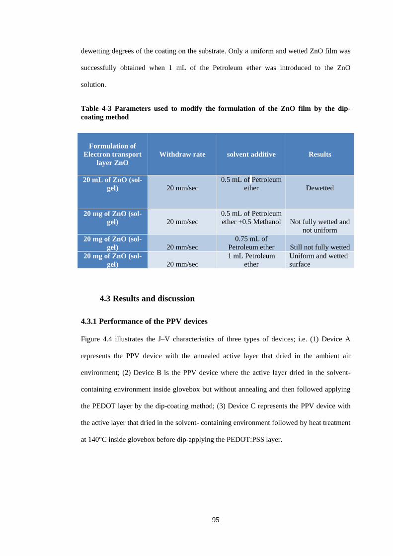
95
dewetting degrees of the coating on the substrate. Only a uniform and wetted ZnO film was
successfully obtained when 1 mL of the Petroleum ether was introduced to the ZnO
solution.
Table 4-3 Parameters used to modify the formulation of the ZnO film by the dip-coating method
Formulation of
Electron transport layer ZnO
Withdraw rate
solvent additive
Results
20 mL of ZnO (sol-gel)
20 mm/sec
0.5 mL of Petroleum ether
Dewetted
20 mg of ZnO (sol-gel)
20 mm/sec
0.5 mL of Petroleum ether +0.5 Methanol
Not fully wetted and
not uniform 20 mg of ZnO (sol-
gel)
20 mm/sec 0.75 mL of
Petroleum ether
Still not fully wetted 20 mg of ZnO (sol-
gel)
20 mm/sec 1 mL Petroleum
ether Uniform and wetted surface
4.3 Results and discussion
4.3.1 Performance of the PPV devices
Figure 4.4 illustrates the J–V characteristics of three types of devices; i.e. (1) Device A
represents the PPV device with the annealed active layer that dried in the ambient air
environment; (2) Device B is the PPV device where the active layer dried in the solvent-
containing environment inside glovebox but without annealing and then followed applying
the PEDOT layer by the dip-coating method; (3) Device C represents the PPV device with
the active layer that dried in the solvent- containing environment followed by heat treatment
at 140°C inside glovebox before dip-applying the PEDOT:PSS layer.

96
Figure 4.4. J-V characteristics of three types of devices; 1) Device A for the dip-coated active layer dried at the normal air environment; 2) Device B for the dip-coated active layer dried at the solvent-containing environment without annealing; 3) Device C for the dip-coated active layer dried at the solvent-containing environment followed by annealing
Summary of the performance parameters is listed in Table 4.4. Device A exhibits a low PCE
of 1.32% mainly because of the low short current density of 4.67 mA/cm2 and the low fill
factor (FF) of 51%. This result is much lower than that of the PPV devices which produced
by the spin-coating method inside the glovebox [209].Two potential reasons can be assigned
that caused the reduction of PCE; (1) oxidation of the active layer when it dried in the
normal air condition compared with those devices produced inside the glovebox; (2)
moisture effects on the active layer due to the aqueous PEDOT:PSS solution applied by the
dip-coating method. When the active layer was placed in the solvent-containing
environment for drying, Device B had an improved PCE of 2.61% due to the significantly
increased short current density at 9.7 mA/cm2. The morphology of the active layer has been
altered by the extended drying rate, which enhanced the PCE of PPV devices. The PCE of
Device C further reached to 3.46% when the dip-coated active layer was annealed at 140°C
before the PEDOT:PSS layer was applied. Heat treatment increased the moisture resistance
of the active layer. The enhanced current density and FF are the main reasons for the

97
improved PCE, reaching 10.61 mA/cm2 and 59% respectively for Device C. Devices A and
B have displayed a close performance in their FF. However, Device A dried in air but
annealed at high temperature while Device B dried in the solvent-containing environment
without annealing. The interesting results may be worth carrying out further investigation in
order to fully understand the reasons behind the different characteristics of the three types of
devices.
Table 4-4 Photovoltaic performance of the PPV devices; (1) Device A for the dip-coated active layer dried in the normal air environment; (2) Device B for the dip-coated active layer dried in the solvent-containing environment without annealing; (3) Device C for the dip-coated active layer dried at the solvent-containing environment and followed by annealing
OPV devices Voc (V)
Jsc (mA/cm2)
FF (%) PCE (%)
Device A 0.55 4.67 51.0 1.32
Device B 0.54 9.70 49.8 2.61
Device C 0.55 10.61 59.0 3.46
4.3.2 Characterisation of the active layer
Figure 4.5 indicates the UV–Vis absorption spectra of the P3HT:PCBM active layers
deposited by the dip-coating technique. The P3HT:PCBM active layer for Device B exhibits
little higher light absorption intensity than that for Device A. They all show the
characteristic absorbing peaks at around 520, 550, and 610 nm for the P3HT polymer. A
light absorption increase was obtained after the dip-coated active layer dried in the solvent-
containing environment was followed by the cure at 140°C.

98
Figure 4.5 Light absorption spectra of the P3HT/PCBM blend of the devices; 1) Device A for the dip-coated active layer dried in the normal air environment; 2) Device B for the dip-coated active layer dried in the solvent-containing environment without annealing; 3) Device C for the dip-coated active layer dried in the solvent-containing environment and followed by annealing
Three peaks, one at 510 and two shoulders at 550 nm and 610 nm separately show the
enhanced absorption in comparison with the active layer without the thermal annealing. The
increase in light absorption is one of the main reasons that contributes to the increased short
current density and hence the PCE for Device C. The X-ray diffraction (XRD)
measurements were further performed to characterise the structure of the active layers; the
obtained XRD patterns of the P3HT:PCBM films are shown in Figure 4.6.

99
Figure 4.6 XRD patterns of the P3HT:PCBM films; 1) Device A for the dip-coated active layer dried in the normal air environment; 2) spin-coating derived active layer with annealing as a reference ; 3) Device B for the dip-coated active layer dried in the solvent-containing environment without annealing; 4) Device C for the dip-coated active layer dried in the solvent-containing environment and followed by annealing
A strong peak at around 5.40° appears for all types of the P3HT:PCBM active layer
fabricated by different methods. The XRD pattern of the active layer by the spin-coating
method in the glovebox is also presented in Figure 4.6 as a reference. Device A illustrates
slightly smaller intensity of the peak at 5.40° than that of the spin coated sample. As shown
in Figure 4.4 since Device A exhibits much lower PCE value than that of the spin-coating
derived device, it can be inferred that the reduced PCE could be caused by moisture which
results from the following PEDOT:PSS dip-coating. Device B shows increased peak
intensity at 5.40° compared with Device A, which confirms that the crystallinity of the
active layer was improved by the extended drying rate of the active layer, leading to the
increased PCE. The intensity of the diffraction peak of the active layer at 5.40° further
increased after heat treatment of device C, demonstrating more oriented structures formed
between the inter-chain spacing of the P3HT polymers after the parallel layers that are
100
associated with the interdigitated alkyl chains. This result corresponds to the increased light
absorption and thus improved the PCE of Device C.
4.3.2.1 Morphologies of the active layer
AFM measurements were also carried out in order to investigate the morphologies of the
surfaces of the three types of active layers and to better understand the mechanism behind
the different performance of the studied PPV devices; the obtained AFM results are shown
in Figure 4.7. It appears from Figure 4.7a that the surface of the active layer for Device A is
rougher than that of Device B and C when it dried in the normal air condition. The faster
drying rate caused the active layer to become solid thin film more quickly. The fast
solidification of the active layer did not allow enough time for even distribution within the
film, leading to a rougher morphology in comparison with that of Device B and C, as shown
in Figure 4.7a. The root mean square roughness derived from the AFM image of the active
layer of Device A is 3.71 nm. Active layer of Device B was dried in the environment of
organic solvents, which has led slower drying rate. The AFM image of the active layer for
Device B shows improved roughness compared to that of Device A as shown in Figure 4.7b.
As a result the root mean square roughness in this layer has reduced to 3.31 nm. The
extended drying time of the active layer has allowed the interpenetrating networks more
mobility to arrange regularly to form a uniform film. Figure 4.7c displays the morphology
of the active layer for Device C. Subjecting the active layer to thermal annealing has further
smoothed the surface morphology of the active layer. The donor and acceptor were more
evenly arranged in the blend and the dense interpenetrating networks have formed. This is
evidenced by the reduced z-axis from 26.8 nm in the case of Device A to 18.6 nm for
Device C as shown in Figure 4.7c where the root mean square roughness becomes 3.09 nm.
AFM images confirm that the morphologies of the active layers have been modified with
different processing methods, which has contributed to the improved PCE of the PPV
devices.

101
Figure 4.7 AFM images of the active layers for a) Device A; b) Device B; c) Device C

102
4.3.2.2 Morphologies of HTLs and ETLs
Morphologies of the spin and dip coated ZnO and PEDOT:PSS layer were compared
separately using the AFM measurements. The spin and dip coated ZnO and PEDOT:PSS
layers shown to exhibit quite different features, as illustrated in Figure 4.8&4.9. The spin-
coated ZnO in Figure 4.8a presents a slightly smoother surface as depicted from the height
colour changes while the dip coated ZnO thin film in Figure 4.8b shows a smaller-
nanoparticles- bonded denser thin film.
Figure 4.8 AFM images of the ZnO thin films; a) by the spin coating method; b) by the dip-coating method

103
Compared to the spin-coated ZnO thin film, the dip-coated ZnO thin film had a slower
drying rate, which explains the formation of the denser thin film. Both films also show some
valleys in height in their morphologies and different sized nanoparticles owing to different
formulation of both solutions. Figure 4.9 shows the morphologies of the PEDOT:PSS layers
obtained by the two coating methods. In comparison with the ZnO thin film, the spin-coated
PEDOT:PSS thin film in Figure 4.9a demonstrates the same smoother surface than the dip-
coated PEDOT:PSS layer.
Figure 4.9 AFM images of the PEDOT:PSS thin films; a) by the spin coating method; 2) by the dip-coating method

104
However, the spin-coated PEDOT:PSS thin film demonstrates a fully different morphology
than the dip-coated PEDOT:PSS layer in Figure 4.9b. It appears to exhibit a nano-wire or
fibre-like constituted thin film, nevertheless, the dip-coated PEDOT:PSS thin film
demonstrates larger sized- nanoparticles formed morphology. The root mean square
roughness of the spin-and dip-coated PEDOT:PSS is 1.56 nm and 2.91 nm, respectively.
The difference in morphologies of the PEDOT:PSS thin films by different coating methods
may affect the charge transport resistance of the PEDOT:PSS HTL.
4.4 Conclusion
Solution processed inverted PPV devices were produced by the dip-coating method. The
best P3HT:PCBM inverted PPV device achieved a PCE of 3.4%. The drying method of the
P3HT:PCBM active layer significantly affected the performance of the fabricated PPV
devices after the sample was withdrawn from the solution. When the active layer dries at a
slower rate, it presents smoother morphologies and more oriented structures. Thermal
annealing can further improve its surface roughness and also enhance its crystallinity. The
aqueous solution of the PEDOT:PSS has its effect on the pre-deposited P3HT:PCBM active
layer. The spin and dip-coating PEDOT:PSS thin films present significantly different
morphologies owing to different solvents used and different processing which might impact
on the performance of the PV devices.

105
Morphological studies of perovskite solar cells Chapter 5 -
5.1 Introduction
In the past few years, organometal halide perovskite (CH3NH3PbI3) has emerged as
one of the most prominent candidates for photovoltaic devices due to its
distinguished optical and electrical properties [171]. These materials can be
fabricated using solution-processing methods at low cost and ease of procedure
compared to the Si-based solar cells [133,210–212]. The power conversion
efficiency (PCE) of perovskite solar cells has been aggressively approaching that of
crystalline silicon solar cells [134]. Very recently, the certified performance of
perovskite solar cells dramatically increased to 22.1 %, making them a potential
competitor to the Si-based solar cells [213].
Currently, a planar heterojunction structure is widely used to fabricate typical
perovskite solar cells via the co-evaporation method or solution-processed
deposition method [124]. The expensive fabrication cost and process complexity of
the vacuum deposition method [142] lead to broad interests in the solution-
processed method. However, one of the biggest challenges that dominates the
performance of the solution-processed perovskite solar cells is to control the
morphologies of the perovskite films [118]. It is closely linked to many physical
properties in solar cells including exciton diffusion length, charge carriers
dissociation efficiency, and charge transport to the electrodes [156]. Also, photons
absorption efficiency and shunting paths are reliant on the morphology and the
quality of the perovskite films [117]. The crystallization behavior of the perovskite
films is affected by many factors such as using one-step or two-step methods, the
precursor concentrations, additives in the one-step method, thickness of the pre-

106
coated lead iodide (PbI2), allowed-reaction-time (Art) between PbI2 and
methylammonium iodide (MAI) in the two-step method before casting the mixture
into perovskite thin films, and thermal annealing [118]. Although many efforts have
been explored to obtain high-quality perovskite thin films, there are still extensive
studies need to be carried out in order to achieve highly reproducible defect-free
perovskite thin films.
In this chapter, investigations into control over the morphology of the perovskite
films using the low-temperature (TSSCM) were presented. (OSSCM) was also
studied for comparison with the TSSCM. The morphologies of the produced
perovskite thin films will be demonstrated and discussed in detail. The perovskite
films by both methods were characterised using scanning electron microscopic
(SEM), UV-vis spectroscopy, and X-ray diffraction (XRD) measurements. Different
concentrations of the MAI solutions and different allowed-reaction-times (Art)
between PbI2 and MAI, and various thermal annealing methods were investigated.
5.2 Experimental methods for perovskite films and solar cells by OSSCM
The one-step spinning deposition method (OSSCM) was used to fabricate the
perovskite thin film samples for various purposes including study of the produced
solar cells properties and crystallisation behaviour of the perovskite films. The PHJ
PV structure was schematically presented in Figure 5.1, where it contained thin
films of ITO/PEDOT:PSS/CH3NH3PbI3/PCBM/BCP/Au, respectively. Pre-
structured ITO-coated glass substrates with sizes of ~ 20 x 25 mm were cleaned
according to the procedure which was presented in section 3.2.8. The cleaned ITO
substrates were spin-coated at 3000 r.p.m by the PEDOT:PSS solution and followed
by heating at 140°C for 10 min.

107
Figure 5.1 Schematic diagram of the fabrication processes of each layer of the perovskite solar cells using OSSCM
The halide perovskite precursor solution was produced by blending lead iodide
(PbI2) and methylammonium iodide (MAI) at the molar ratio 1:1 in anhydrous N, N
-dimethylformamide (DMF) solvent. Then, 30 l of the blended solution (PbI2 and
MAI) was spun at 5000 r.p.m for 20 sec. The obtained thin films were subjected to
heat treatment at 100°C for two hours. The PCBM film was then deposited by the
spin-coating method from the PCBM solution on top of the formed perovskite thin
film at 2000 r.p.m followed by heat treatment at 100°C for 30 min. A thin film of
BCP (~10 nm) was deposited by the spin-coating method on top of the BCPM film
as the electron buffer layer prior to the deposition of Au thin film of ~100 nm as the
top electrode by the vacuum sputtering method.

108
5.3 Results and discussion
5.3.1 Morphological studies of the CH3NH3PbI3 film fabricated via OSSCM
The morphology of the CH3NH3PbI3 thin film produced by the OSSCM was
examined using SEM measurements. Figure 5.2 illustrates porous fabric structures
of the perovskite thin films. It was suggested that the porous structure is owing to
the prompt reaction between the two precursors of MAI and PbI2 and a rapid
crystallisation of the formed intermediate phase by the subsequent thermal annealing
processes[134].
Figure 5.2 SEM images of the perovskite film fabricated via OSSCM
5.3.2 Light absorption and crystal structures of the CH3NH3PbI3 films
fabricated via OSSCM
The UV-Vis absorption spectra and X-ray diffraction measurements were carried out
to investigate the optical properties and crystal structures of the CH3NH3PbI3 thin
film obtained by OSSCM respectively. Figure 5.3 shows a typical light absorption
spectrum of the obtained perovskite film in the wavelength range 350 to 800 nm.
The absorption onset appears at 800 nm which is in agreement with the reported

109
optical bandgap of ~ 1.52 eV for methylammonium halide perovskite CH3NH3PbI3
[80,214,215].
Figure 5.3 UV-Vis absorption spectrum of the CH3NH3PbI3 film fabricated via OSSCM
Figure 5.4 shows the X-ray diffraction pattern measured for the CH3NH3PbI3 thin
film produced by the OSSCM. Two main peaks at 2Ɵ of 14.2° and 28° in addition to
other peaks at 19°, 24°, 31°, 41° and 43° are presented, confirming the formation of
the perovskite structure.
Figure 5.4 X-ray diffraction pattern of the CH3NH3PbI3 film fabricated via OSSCM

110
5.3.3 Performance of the perovskite solar cells fabricated via OSSCM
In total, 30 solar cells based on CH3NH3PbI3 thin film produced by the OSSCM were
studied and have all shown a very poor performance. The best power conversion
efficiency (PCE) of 3.45% was achieved as a result of short circuit current (Jsc),
open circuit voltage (Voc) and fill factor (FF) of 9.97 mA, 0.933 mV and 0.37
respectively. Figure 5.5 illustrates the current-voltage (J-V) characteristics of the
best-performing perovskite device fabricated by OSSDM. Table 1 summarises the
obtained photovoltaic parameters of the perovskite solar cells fabricated by
OSSDM.
The poor performance of the perovskite devices was mainly due to their porous
structures in morphologies of the perovskite films, resulting in the reduced light
absorption and the current leakage in solar cells as a result of shunt paths formation.
Figure 5.5 J-V characteristics of the CH3NH3PbI3 solar cell fabricated via OSSCM

111
Table 5-1 Summary of parameters for the best CH3NH3PbI3 solar cells fabricated by OSSCM
Perovskite
solar cell
device
Jsc
(mA/cm2)
Voc
(mV)
FF PCE
(%)
The best
device
9.97 0.933 0.37 3.45
5.4 Morphological studies of the perovskite films using (TSSCM)
5.4.1 Morphology study of PbI2 thin films
Figure 5.6 shows the surface morphology of the PbI2 thin film produced from the
lead iodide (PbI2) in DMF solution with the DIO additive. The PbI2 is shown to
exhibit a connected and uniform needle-like nano-crystalline structure. This unique
structure allowed the PbI2 phase to react with the added MAI in the following stage
to form the halide perovskite thin films.
Figure 5.6 SEM image of PbI2 based DIO film

112
5.4.2 The morphology of the CH3NH3PbI3 films fabricated via TSSCM with
different concentrations of the MAI solution.
The growth behaviour of the perovskite crystals was investigated using different
MAI concentrations and different allowed reaction time (Art) between MAI and
PbI2 by the two-step method. Thermal annealing of the perovskite thin films was
carried out at 100°C for 2 hours.
Figure 5.7 shows the colour change of the applied MAI solution that was kept on top
of the pre-coated PbI2 film at different extended reaction time between MAI and
PbI2. As can be observed, the colour of the solution gradually changed from yellow
to brown and finally to dark brown as the reaction time increased from one sec to
one minute.
Figure 5.7 Pictures of the PbI2 film (left, centre left) and the MAI solution after being applied onto the pre-deposited PbI2 thin film with different extended reaction time between MAI and PbI2: b) 1 sec, c) 20 sec and d) 60 sec
The perovskite films were fabricated by the procedures as followed; a super
saturated solution of PbI2 was deposited onto the glass slides and then thermally
annealed at 70 °C for 8 min. Subsequently, a 120 µl of the MAI solution was
deposited onto the cured PbI2 layer following different reaction time and then
followed by thermal annealing at 100 °C for 120 min.
A processing model to describe the formation of the perovskite thin films with
various concentrations of the MAI solutions (0.5, 0.8, 1.0 and 1.2 wt %) is

113
schematically presented in Figure 5.8. When the MAI solution reached the pre-
coated PbI2 crystals, nucleation of an intermediate phase of perovskites only
happened in those areas where the MAI concentration must be greater than a
concentration threshold (Ck). Lower concentrations than Ck did not result in the
intermediate perovskite phase for the crystal growth. Reaction time between MAI
and PbI2 allows the growth of an intermediate phase of perovskite. This intermediate
phase is then transformed into full perovskite phases after thermal annealing at
100°C. When a low concentration of the MAI solution 0.5 or 0.8 wt % was applied
onto the pre-formed PbI2 film as shown in Figure 5.8, only a perturbation in
concentration led to some areas with a locally high concentration of the MAI, which
resulted in the formation of a sporadically distributed intermediate phase of
CH3NH3PbI3. Only when the concentration of the MAI solution increased to 1.0 wt
%, the distributed amount of MAI on the whole surface area of the PbI2 film was
maintained at larger than the concentration threshold, and a gradually controlled
crystal growth happened. After maintaining the structure for about one minute, the
thin film with a uniform intermediate perovskite phase was formed. Longer growth
time (60 sec) and higher concentration of MAI (1.2 wt%) will lead to the lift-off of
the intermediate perovskite phase from the substrate, which then reduced the
thickness of the final perovskite film by the subsequent spin-coating process.

114
Figure 5.8 Schematic diagram of the processing model for the formation of the perovskite thin films with different concentration of the MAI solutions via TSSCM

115
Scanning electron microscopy (SEM) measurements were then used to characterise
the morphologies of the perovskite films obtained by the TSSCM as shown in
Figure 5.9 & and Figure 5.10. Different concentrations of the MAI solutions at 0.5
wt%, 0.8 wt%, 1.0 wt% and 1.2 wt% were separately utilized to apply onto the pre-
coated PbI2 thin film with different reaction time of 20 and 60 sec, and followed by
thermal annealing of the perovskite films at 100°C for 2 hours. When the lowest
concentration of 0.5 wt% MAI was added onto the pre-coated PbI2 film, the size of
the perovskite crystals increased from ~ 0.7 µm for a 20 sec reaction time to ~ 1.0
µm for a 60 sec reaction time as seen in Figure 5.9a &b.
Comparing Figure 5.9a with Figure 5.9b, the slightly dissolved PbI2 film was
observed except sporadically distributed perovskite crystals. The formed perovskite
crystals did not cover the whole surface. In other words, most PbI2 crystals were
only slightly dissolved by the MAI solution. The low MAI concentration led to low
nucleation density and thus low crystallisation for perovskites. Further increase in
the reaction time between MAI and PbI2 did not make any contributions to the
enhancement of the nucleation density on the surface of the PbI2 film. Interestingly,
with the increase of the MAI concentration to 0.8 wt%, the crystallisation occurred
with an increased surface coverage on the PbI2 thin film as indicated in Figure
5.9c&d. However, the size of the perovskite crystals decreased to ~ 0.4 µm
regardless of how long the reaction time would be.

116
Figure 5.9 SEM images of the perovskite films fabricated via TSSCM at the 0.5 wt % MAI solution for reaction time: a) 20 sec; b) 60 sec.; and at the 0.8 wt % MAI solution at reaction time: c) 20 sec.; d) 60 sec. Two different measurement scales are used for each studied sample

117
With a further increase of the MAI concentration to 1.0 wt%, the coverage of the
perovskite surface reached to all the pre-coated PbI2 surface; meaning that all PbI2
crystals have reacted with the MAI solution to form perovskites as shown in Figure
5.10a&b. Again, I have it was observed that the size of the perovskite crystals
continued to decrease to about 0.2 µm. Nevertheless, when the concentration of the
MAI solution further increased to 1.2 wt. %, pore defects among the smaller nano-
sized perovskite crystals were revealed as shown in Figure 5.10c&d. According to
SEM images in Figures 5.9&5.10, the size of the perovskite crystals in the film did
not change with extended reaction time from 20 to 60 sec when using high
concentrations of 0.8, 1 and 1.2 wt % MAI solutions. This confirms that the size of
crystals in the perovskite film was determined in the initial reaction stage when the
MAI solution came into contact with the pre-coated PbI2.

118
Figure 5.10 SEM images of the perovskite films fabricated via TSSCM at the 1 wt % MAI solution for reaction time: a) 20 sec.; b) 60 sec.; and at the 1.2 wt % MAI solution for reaction time: c) 20 sec.; d) 60 sec. Two different measurement scales are used for each studied sample

119
5.4.3 The impact of reaction time between MAI and PbI2 on the morphology of
the perovskite film produced from 1.0 wt% MAI solution
The growth behaviour of the perovskite crystals was then investigated according to
different reaction times between MAI and PbI2 at 5, 20, 60 and 180 sec respectively
with the 1.0 wt % MAI solution as shown in Figure 5.11. Similarly, no change in the
size of the perovskite crystals was observed when using different reaction times. The
size of the perovskite crystals in the film was ~ 200 nm, however, at 5 sec reaction
time, many porous defects existed in the perovskite film (Figure 5.11a) while for 20
sec reaction time, pores were significantly reduced (Figure 5.11b). A uniform and
fully connected perovskite film without any pores or other defects was obtained
when applying the 1.0 wt % MAI solution for 60 sec reaction time as shown in
Figure 5.11c. Interestingly, the polycrystalline structures with clear grain boundaries
in the perovskite film disappeared upon increasing the reaction time to 180 sec,
resulting in poor quality perovksites (Figure 5.11d).
Figure 5.11 SEM images of the perovskite films fabricated via TSSCM at the 1.0 wt % MAI concentration with different reaction time for: (a) 5 sec; (b) 20 sec; (c) 60 sec; and (d) 180 sec

120
Based on these investigations, the best quality perovskite thin film was only
achieved when the 1.0 wt% MAI solution was added on the pre-deposited PbI2 thin
film with 60 sec reaction time allowed between MAI and PbI2 as shown in Figure
5.12.
Figure 5.12 SEM images of the perovskite films fabricated via two-step method at fixed concentration of MAI at 1.0 wt% with loading time of MAI at 60 sec
5.4.4 The impact of reaction time between MAI and PbI2 on the optical
properties and crystal structures of the perovskite thin films
UV-Vis absorbance and X-ray diffraction patterns were used to further understand
the effect of reaction time between MAI and PbI2 on the formation of the perovskite
thin films.
Figure 5.13 displays the UV-Vis spectra of the perovskite thin film produced from
the 1.0 wt% MAI solution with different loading time. The same absorption onset
was observed for all perovskite samples at ~ 780 nm. Furthermore, the absorbance
increased gradually for the perovskite films after increasing reaction time from 5 to
60 sec between MAI and PbI2 at the wavelength range of 420-780 nm. The fully-
covered-surface and uniform morphology of the perovskite film by 60 sec reaction
time was one of the main reasons to contribute to the improvement in the light
absorption. However, a considerable reduction in the light absorption was observed
for the perovskite film produced with further increased reaction time to 3 min.

121
Figure 5.13 UV-Vis absorption spectra of the CH3NH3PbI3 films fabricated with the 1.0 wt% MAI solution at different loading times
Figure 5.14 illustrates X-ray diffraction patterns for the perovskite films with
different loading times. Two phases were obtained for the perovskite film with 5 sec
reaction time, the residual PbI2 phase “●” at 8.8° and 12.8° and the perovskite phase
“ ” at 14.2, 25, 28, 31, 41 and 51o, separately. Increasing reaction time between
MAI and PbI2 to 20 sec resulted in the significantly reduced peak intensity of the
PbI2 phase. Highly crystallised perovskites were obtained with reaction time at 60
sec without showing any residual PbI2 phase in the XRD pattern shown in Figure
5.14. Furthermore, decomposition of the perovskite film was confirmed after further
increasing the reaction time to 180 sec, showing two new peaks at 8.8° and 12.8° in
the XRD pattern.
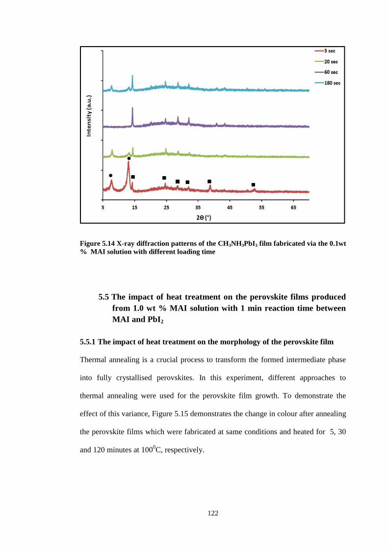
122
Figure 5.14 X-ray diffraction patterns of the CH3NH3PbI3 film fabricated via the 0.1wt % MAI solution with different loading time
5.5 The impact of heat treatment on the perovskite films produced from 1.0 wt % MAI solution with 1 min reaction time between MAI and PbI 2
5.5.1 The impact of heat treatment on the morphology of the perovskite film
Thermal annealing is a crucial process to transform the formed intermediate phase
into fully crystallised perovskites. In this experiment, different approaches to
thermal annealing were used for the perovskite film growth. To demonstrate the
effect of this variance, Figure 5.15 demonstrates the change in colour after annealing
the perovskite films which were fabricated at same conditions and heated for 5, 30
and 120 minutes at 1000C, respectively.

123
Figure 5.15 Pictures of PbI2 and perovskite thin films after thermal annealing: a) PbI2 film; perovskite thin films annealed for b) 5 min; c) 30 min; d) 120 min
SEM images of the perovskite films in Figure 5.16 show that the grain size of the
perovskite crystals did not greatly change as thermal annealing time increased.
This result indicated that the size of the perovskite crystals was determined during
the initial reaction stage between MAI and PbI2. However, significant improvement
in the morphology and an enhanced interconnection between the perovskite crystals
was achieved when thermal annealing time gradually increased from 5 minutes to
120 minutes.
Figure 5.16 SEM images of the perovskite films fabricated via the two-step method at the 1.0 wt% MAI solution with 60 sec. loading time under various thermal annealing times: a) 5 min; b) 30 min; c) 60 min; d) 120 min
a b c d

124
5.5.2 The impact of heat treatment on optical and crystalline structure
properties of the perovskite film
To further understand the influence of thermal annealing on the formation of
perovskite films, UV-vis absorbance and X-ray diffraction patterns were recorded
for the perovskite films as shown in Figure 5.17 and Figure 5.18 respectively. A
wide absorption band of the perovskite film was observed after 5 minutes thermal
annealing, confirming the formation of perovskite structures as shown in Figure
5.17.
Additionally, it is also revealed that the absorbance of the perovskite film
significantly increased in the wavelength range of 400-600 nm with increased
thermal annealing times of 30, 60, to 120 min. This improvement in the light
absorption is owing to the enhancement in the crystallinity of the perovskite
structures and the improvement in the surface morphology. The onset in the light
absorption is shown to occur at ~ 780 nm for all studied perovskite samples.
Figure 5.17 UV-Vis absorption spectra of the perovskite films annealed at 100 °C for 5, 30, 120, and 180 min, separately

125
X-ray diffraction (XRD) test was carried out to further explore the influence of
thermal annealing on the degree of crystallinity of the perovskite films. As
illustrated in Figure 5.18, the PbI2 phase at 2Ɵ of 12.2° in X-ray diffraction pattern
has disappeared after annealing the perovskite film for 5 minutes, which indicates a
quick phase transformation. The same peaks in the diffraction pattern were observed
for all the perovskite films that were annealed for a prolonged periods of 30, 60 and
120 minutes. However, the full width at half maximum (FWHM) of the diffraction
peak at 14.2° decreased progressively with the gradually increased thermal
annealing time for the perovskite films from 5 to 120 min. The FWHM value at
14.2° decreased from 0.251 for the perovskite film annealed for 5 min to 0.1571
after 2 hours thermal annealing as shown in table 2, indicating a high degree of
crystallinity in the perovskite films.
Figure 5.18 X-ray diffraction patterns of the CH3NH3PbI3 thin films fabricated via TSSCM with different heat treatment times

126
Table 5-2 The full width at half maximum of the diffraction patterns at 14.2° for the perovskite film with different thermal annealing times
5.6 Conclusions
OSSCM and TSSCM were utilized to fabricate thin films of CH3NH3PbI3.
Morphologies of the formed perovskite thin films by these methods were
investigated. Without any additives from the mixed precursors of MAI and PbI2,
porous and fabric morphology of the perovskite film was obtained by OSSCM via
SEM observation. This is mainly ascribed to the fast crystallisation of the
intermediate phase in the blended precursors when thermally annealing the formed
film. [134]. In the two-step method, different parameters for the perovskite film
including different concentrations of the MAI solution different loading times (Art)
and various thermal annealing conditions were used to investigate the crystallisation
behaviour of the perovskite films. The best morphology of the perovskite film was
obtained when the 1.0 wt % MAI solution was used with reaction time of 60 sec was
allowed between MAI and PbI2 and followed by thermal annealing at 100°C for 2
hours.
Heat treatment time Full width at half maximum
(FWHM)
5 min 0.251
30 min 0.228
60 min 0.203
120 min 0.157

127
Highly reproducible perovskite solar cells via Chapter 6 -controlling the morphologies of the perovskite thin
films by the solution-processed two-step method
6.1 Introduction
Organometal halide perovskites have received significant interests in the last few
years due to their superior optical and electrical properties. They demonstrated
highly-efficient capability in converting light into electricity with low cost
precursors and cheap solution-processed methods in fabricating solar cells
[47,150,161,210,216–218]. Power conversion efficiency (PCE) has considerably
jumped from 3.8% in 2009 [77] to the certified efficiency of 22.1 % in 2016 [215]
with two types of typical device architectures; i.e. solar cells based-on TiO2
structures [219–224] or those based-on phenyl-C61-butyric acid methyl ester
(PCBM) planar heterojunction (PHJ) structures [129,225–228]. In order to achieve
high PCE solar cells, controlling the morphology of the perovskite thin films is one
of the major challenges. In the published studies, perovskite films were produced via
various methods such as vacuum thermal deposition and solution-processed
deposition by either one-step or two-step processes. Good quality perovskite films
were obtained by both aforementioned methods with high PCE solar cells. However,
the major obstacle for the thermal evaporation method is due to its high-cost vacuum
systems and complicated processes. Furthermore, in order to control the morphology
of the perovskite thin films in the one-step solution-processed method, two main
routes were utilised, i) adding additives into the precursor solution of perovskites; ii)
by a so-called solvent engineering technology [215]. Nevertheless, it was found that
uniform morphologies are difficult to re-produce in the one-step method owing to
their uncontrollable crystallisation rate during the fabrication processes [22].

128
Therefore, the two-step method has been widely adopted as an efficient way to
control the morphology of the perovskite layer for both TiO2-based and the PCBM-
based perovskite solar cells, mainly because the concentration in one of the
precursors can be selected to control their reaction and crystallisation rates.
For the TiO2-based perovskite solar cells, different techniques were used to control
the morphologies including vapor-assisted solution-processes [138], the halide
sources mixing method [229], low-temperature gas-solid crystallisation processes
[230], solution chemistry engineering [142], anti-solvent vapour-assisted
crystallisation processes [231], and the two-step ultrasonic spray deposition method
[211]. However, these methods are complicated although high-performance solar
cells were obtained in many cases and appeared in the published literature.
Furthermore, the TiO2 layer has to be sintered at around 500°C for the TiO2-based
solar cells [150]. Alternatively, the two-step fabrication method for the PCBM-based
perovskite solar cells presents the low-temperature alternative processing route with
the incredible benefit of simple procedure to control the morphologies of the
perovskite films.
Different strategies have been used to control the crystallisation and to improve the
morphologies of perovskite thin films in the PCBM-based perovskite solar cells.
Shen et al. used the two-step annealing process to fabricate CH3NH3PbI3 (assisted
by doping with PbCl2) perovskites films [148]. They found that thermal annealing
improved the surface coverage and crystallisation of the perovskite films. A PCE of
9.1% was achieved for solar cells based on the perovskite obtained by this method
[148]. Haung et al. claimed that solvent annealing used in the fabrication of the
perovskite films is an efficient technique to enhance the crystallinity of perovskites,
which results in obtaining 1 m grain sizes of perovskites. They added the DMF

129
solvent at the edge of Petri dish where it contained the perovskite film sample during
thermal annealing. They expected that the DMF vapour could penetrate into the
perovskite film, achieving 15.6% PCE solar cells [153]. Dai's group used a
technique (called layer-by-layer) to control the morphology of the perovskite film.
The PbCl2 thin film was deposited by thermal evaporation, followed by dipping the
sample into a solution of CH3NH3I/IPA for several times to form the uniform
perovskite layer [232].
Both solvent annealing and thermal annealing play their key roles in controlling the
crystal growth of perovskites for the improvement of their morphologies in the two-
step method. However, many other factors significantly affect the solvent annealing
processes; these include type and vapour pressure of solvents, surroundings, and
thermal annealing conditions such as annealing temperature, duration and ramping
level [142]. On the other hand, the reaction time between the pre-coated metal halide
after being dipped into the MAI solution requires accurate control [138].
In this chapter, we present a simple route to control the morphology of our
perovskite films by the two-step deposition method in the fabrication of PCBM-
based PHJ solar cells. Through wide investigations of alternating the concentration
of MAI and its reaction time with the pre-deposited PbI2 film, high-performance
perovskite films were reproducibly obtained, resulting in solar cells with PCE of
15.01%. The morphology and crystallinity of perovskite films were extensively
investigated by SEM and XRD, respectively. In addition, UV-Vis absorption spectra
test was used to check the optical properties of the produced films.

130
6.2 Device structure and experimental methods
The structure of the produced PHJ PV devices is schematically presented in Figure
6.1; the structure encompasses thin film of ITO/PEDOT:PSS/CH3NH3PbI3
/PCBM/BCP/Au, respectively. Pre-structured ITO-coated glass substrates with sizes
of ~ 20 x 25 mm were cleaned according to a procedure which was described in
section 3.2.8. The cleaned ITO substrates were spin-coated at 3000 rpm by the
PEDOT:PSS solution and followed by heating at 140°C for 10 min. The PbI2 thin
film was deposited on top of the PEDOT:PSS film by the spin-coating method at
5000 rpm using the high-purity supersaturated hot solution and then annealed at
70°C for 8 min on a hotplate. The MAI solution with different concentrations (0.8,
1.0, 1.2 wt %) were added on top of the PbI2 thin film and then was kept for a fixed
time of 60 sec to allow for chemical reaction between PbI2 and MAI, followed a
rotation at 5000 rpm using the spin-coater. The obtained thin films were then heated
at 100°C for 2 h. A thin film of PCBM was then deposited by the spin-coating
method from the PCBM solution on top of the formed perovskite thin film at 2000
rpm and followed by heating at 100°C for 30 min. Thereafter, the thin film of BCP
(about 10 nm thick) was spin-coated on top of the BCPM film as the buffer layer
and finally a 100 nm thick Au film was applied as the top electrode on top of the
BCP film using vacuum sputtering method.

131
Figure 6.1 Schematic diagram of the fabrication process for each layer of the perovskite solar cells using TSSCM
6.3 Results and discussion
6.3.1 Cross section structures and surface morphologies of perovskite films
with different concentrations of MAI
In order to disclose the mechanism, surface morphologies of the CH3NH3PbI3
perovskite films have been widely examined in Chapter 5. To better compare with
each other, typical morphologies by SEM were presented here again in Figure 6.2
(left side). Cross sectional images of the perovskite films with different
concentration of MAI at fixed loading time of 60 sec are shown in Figure 6.2 (right
side). The perovskite films were prepared as was explained in section 5.4.2 on
normal glass slides. Figure 6.2a& b illustrate the SEM top-surface and cross section
images of the final perovskite film fabricated by the 0.8 wt % MAI solution. Figure

132
6.2a shows block morphologies of the perovskite crystals measured at ~ 400 nm in
addition to the PbI2 crystals which were dissolved after applying 0.8 wt % MAI
solution, this is due to the low concentration of MAI, where the corresponding
thickness of the perovskite film was ~400 nm as shown in Figure 2b. These nano-
sized CH3NH3PbI3 polycrystals did not connect together and considerable residual
PbI2 phases existed in the film as it shown later by X-ray diffraction test in section
6.3.2. However, interconnected blocks of CH3NH3PbI3 polycrystals without any
residual PbI2 phase were formed after applying the MAI solution at a concentration
level of 1.0 wt % onto the pre-coated PbI2 film as illustrated in Figure 6.2c & d. It
was found that the intermediate perovskite phase was fully transferred to perovskite
crystals after applying 1.0 wt % of MAI to the pre-coated PbI2. The surface
morphology of the cuboids CH3NH3PbI3 polycrystals reveals a connected and
uniform morphology of the perovskite film with a thickness of ~ 200-220 nm as
illustrated in Figure 6.2d. Furthermore, when the concentration of the MAI solution
was increased to 1.2 wt %, pores among smaller-sized CH3NH3PbI3 polycrystals
were revealed in Figure 6.2e &f. The measured thickness of the perovskite film
showed a significant reduction to ~120 nm.

133
Figure 6.2 SEM top surface and cross section images of the perovskite films with different concentrations of MAI a& b) 0.8 wt %; c& d) 1.0 wt %; e& f) 1.2 wt %

134
6.3.2 Light absorption and crystal structures of the perovskite films with
different MAI concentrations
Light absorption of the formed perovskites was examined to study the impact of the
MAI concentrations on optical the properties of the perovskite films. All perovskite
films with different MAI concentrations show absorption onset at ~ 780 nm as
shown in Figure 6.3, which could confirm the band gap of perovskites at ~1.58 eV.
The perovskite film produced by the low concentration of 0.8 wt% MAI solution
presented the highest thickness as shown in Figure 6.2b and the highest light
absorption was achieved by this film. On the contrast, the perovskite film obtained
by the highest MAI concentration of 1.2 wt % resulted in the lowest thickness and
therefore a significant reduction in the absorption intensity was observed as shown
in Figure 6.3. The perovskite thin film from the 1.0 wt % MAI solution illustrated an
excellent light absorbance between the perovskite films by 0.8 wt% and 1.2 wt%
MAI solutions.
Figure 6.3 UV-Vis absorption spectra of CH3NH3PbI3 films fabricated via TSSCM with different concentrations of MAI (0.5, 0.8, 1.0 and 1.2 wt %) at 60 sec loading time

135
X-ray diffraction (XRD) patterns were used to characterize the crystalline structures
of the perovskite films as presented in Figure 6.4. All perovskite films were
prepared under the same conditions on glass slides of exactly the same size.
Diffraction peaks that belong to CH3NH3PbI3 polycrystals were indicated by “ ”
while the main peaks being assigned to the residual PbI2 phase were illustrated by
“●”. The XRD pattern of the sample from the lowest MAI concentration (0.5 wt%)
reveals different peaks positions at 2Ɵ of 8.2, 12.8, 14.2, 20.0λ, 23.8, 28.4, 31.λ,
40.7, 42.6 and 52 degrees. Most peaks belong to the perovskite structures except the
peaks at 8.2 and 12.8 degrees which are due to the residual PbI2 phase. The high
intensity of these two peaks indicates that considerable residual PbI2 phases are
present in the sample. Increasing the MAI concentration to 0.8 wt % led to more
perovskite phases in the film as it was shown in Figure 6.4, where the two peaks
representing the residual PbI2 phase have significantly reduced. When the MAI
concentration reached to 1.0 wt %, only peaks representing the perovskite phase can
be observed in the XRD pattern, suggesting that all PbI2 phases have changed to
perovskites via reaction.
Figure 6.4 X-ray diffraction patterns of CH3NH3PbI3 thin films fabricated via TSSCM with different concentrations of MAI (0.8, 1.0 and 1.2 wt %) at 60 sec loading time

136
For the sample produced by adding 1.2 wt % MAI concentration, the main peak at
2Ɵ of 14.2 with the highest intensity for the perovskite phase has further reduced
due to the reduction in film thickness.
6.3.3 Performance of the perovskite solar cells
6.3.3.1 Effect of applying different MAI concentrations
The quality of perovskite thin films played a key role in determining the PCE of PV
devices based on these films as the active layers. The concentration of the MAI
solution and reaction time between MAI and PbI2 are crucial to obtain high-quality
perovskite thin films. We have found that reproducible solar cells were achieved
when one minute reaction time was utilized. Therefore, different concentrations of
the MAI solution and one minute reaction time were applied to fabricate perovskite
thin films for our solar cells as was discussed in section 6.2 to compare their PCEs.
As shown in Figure 6.5 for the J-V characteristics curves, the best performance
measured among the PV devices was achieved using the perovskite film fabricated
by the 1.0 wt. % MAI solution on the pre-coated PbI2 thin film.
A summary of the performance of studied devices with the perovskites produced by
different concentrations of MAI solutions is listed in Table 6.1.
Table 6-1 Device performance against different concentrations of the MAI solutions
Concentration of MAI
(wt %)
Voc
(V)
Jsc
(mA/cm²)
FF PCE
(%)
0.8 0.95 11.4 0.38 4.19
1 0.945 20.25 0.64 12.39
1.2 0.93 14.2 0.54 7.2

137
Overall, the solar cells with the 1.0 wt % MAI concentration demonstrated a typical
performance with PCE of 12.39%, short circuit current of 20.25 mA/cm², and fill
factor of 0.70. The high performance was achieved due to the homogeneous and
connected crystals of the perovskite structure and the pure perovskite phase.
However, a reduction in the performance of the perovskite devices was observed
when using 1.2 wt % of MAI solution to fabricate the perovskite layer compared to
using 1.0 wt % of MAI solution. The solar cells presented a low PCE of 7.2%,
owing to the low current density of 14.2 mA/cm2 and low FF of 0.54. The smaller
thickness of the perovskite film from the 1.2 wt % MAI solution and the
perovskite’s porous morphology are assigned as the main reasons for the decreased
PCE.
Figure 6.5 J-V characteristic curves of the CH3NH3PbI3 solar cells fabricated via the two-step method with different concentrations of MAI at 60 sec loading time
By contrast, the PV devices with the perovskite film from the 0.8 wt. % MAI
solution achieved the smallest PCE of 4.19%, presenting the lowest current density
of 11.4 mA/cm2 and very low FF of 0.38. The high portion of the residual PbI2

138
phase in the perovskite thin film was blamed as the main culprit for the poor
performance. Moreover, the second reason for the reduction of PCE was that the
perovskite crystals did not cover the whole surface. All solar cells with the
perovskite film by different MAI concentrations demonstrated reasonable open-
circuit voltage of above 0.9 V.
6.3.3.2 Effects of using two different concentrations of PCBM solutions for the
HTL with or without the BCP buffer layer
Three different perovskite devices were fabricated using the same procedures as
described in Section 6.2. The PCBM layer however was produced with two different
concentrations of 30 and 40 mg/1mL chlorobenzene solution. The solar cells were
also fabricated either with a BCP buffer layer or without a BCP buffer layer. Table
6.2 demonstrates the performance of the perovskite solar cells with various
concentrations of PCBM with or without BCP buffer layer.
Table 6-2 Performance of the perovskite devices with different concentrations of PCBM with or without BCP
Concentration of PCBM with or
without BCP
Voc
(V)
Jsc
(mA/cm²)
FF PCE
(%)
30 mg of PCBM with BCP 0.92 23.5 0.68 14.7
40 mg of PCBM with BCP 0.929 20.2 0.65 12.19
30 mg of PCBM without BCP 0.85 14.7 0.38 4.76
A significant enhancement in the PCEs of the perovskite solar cells with BCP, when
PCBM thin film was deposited at a fixed spin rate of 1000 r.p.m from the 30 mg/1
mL chlorobenzene solution compared to the 40 mg/1 mL solution. The PCE has
jumped from 12.19 % to 14.70 % after inserting a thin film of BCP with lower

139
concentration of PCBM as shown in Figure 6.6. This increase in PCE was due to the
enhancement in fill factor and short circuit current from 0.65 to 0.68 and from 20.2
to 23.5 mA/cm2 respectively. However, there was a substantial reduction in the
performance of the perovskite solar cells when fabricated without a BCP buffer
layer. The PCE is decreased to 4.35 as a result of the decreasing fill factor and short
circuit current of 0.38 and 14.7 mA/cm2 respectively.
The main benefit of using the BCP buffer layer is that it facilitates the collection of
charge carriers from the electron transport layer to the corresponding electrode, and
improves the interfacial layer between the PCBM and the top Au electrode.
Figure 6.6 J-V characteristics of the perovskite devices with different concentrations of PCBM with or without BCP
The best performance of perovskite solar cells was obtained by using 1.0 wt% MAI
solution, PCBM of 30 mg/1mL chlorobenzene solution with BCP buffer layer which
was measured under illumination and under dark surroundings as shown in Figure
6.7. The PCE of 15.01% was attained with high short circuit current of 23.8
mA/cm², fill factor of 0.70, and open circuit voltage of 0.92 mV. Figure 6.8 presents
the performance distribution of 135 solar cells fabricated from the 1.0 wt% MAI

140
solution, PCBM of 30 mg/1mL chlorobenzene solution with BCP buffer layer
showing very good reproducibility.
Figure 6.7 J-V characteristics for the best device under illumination and under the dark condition
Figure 6.8 Performance distribution of 135 solar cells fabricated from the 1.0 wt % MAI solution
6.3.3.3 The hysteresis effect
It has recently been recognised that the phenomenon of hysteresis may occur in
some perovskite solar cells at different scanning rates or at different directions
[228]. The influence of hysteresis on the solar cells has also been investigated in this

141
work. Forward and reverse scanning in the measurements of J-V dependence were
conducted as demonstrated in Figure 6.9. The studied solar cells exhibited
convergent performance in PCE under both the forward and reverse scan directions,
suggesting almost negligible hysteresis effect.
Figure 6.9 J-V characteristics measured under forward and reverse scan directions for the perovskite solar cells with the structure of ITO/PEDOT:PSS/CH3NH3PbI3/PCBM/BCP/Au
The negligible hysteresis is accredited to the reduction in the density of defects due
to the controlled morphologies of perovskite films produced by the two-step
fabrication method [228]. The decent interface between the perovskite layer and the
electron or hole transport layers can be another reason for the mitigation of the
hysteresis effect in the perovskite solar cells [215].
6.4 Conclusions
A low-temperature two-step fabrication method was used to produce high quality
CH3NH3PbI3 thin films for PHJ solar cells. It was found that the concentration of the
MAI solution and reaction time between MAI and PbI2 have a significant impact on

142
the morphologies and crystal growth of the perovskite thin films. Highly replicable
perovskite thin films were fabricated in this work and successfully applied for high
performance solar cells.
For solar cells based on perovskite films produced by the 1.0 wt. % MAI solution
and one minute reaction time, 110 out of 135 devices gave PCE above 13.0 %; the
highest PCE was 15.01%.

143
Blending photoactive polymer with halide perovskite as Chapter 7 -light harvesting layer for solar cells to enhance
stability of devices
7.1 Introduction
Polymer solar cells (PSCs) have received considerable interest in the past twenty
years owing to their potentially low-cost roll-to-roll processing. The power
conversion efficiency (PCE) has steadily increased to ~10% for a single BHJ
photovoltaic device [62,233]. However, the PCE is still too low to occupy a large
market share when competing with 1st generation Si-wafer-based and 2nd
generation thin-film-based solar cells. The low PCE is mainly due to the short
diffusion length of charge carriers within the photoactive conjugated polymer [234–
236], which causes loss of free charge carriers due to recombination. Because of
short charge-carrier diffusion length, planar heterojunction (PHJ) architectures only
result in inefficient PSCs. High-efficiency however is achieved in BHJ PSCs via the
blend of a photoactive polymer with an electron-acceptor material such as phenyl-
C61-butyric acid methyl ester (PC61BM) or phenyl C71 butyric acid methyl ester
(PC71BM) [31]. In addition, organolead halide perovskite-based solar cells more
recently demonstrated highly-efficient capability of converting sunlight into
electricity with low cost precursors and cheap solution-processing methods. The
PCE has significantly increased from 3.8% in 2009 [77] to ~22.1% up to date [213].
The rapid increase in PCE has brought remarkable rise in interest in this fascinating
class of materials. By combining different halides and altering their ratios in
organolead halide perovskites, light absorbance can be tuned to cover a wide range
of wavelengths [168]. However, their poor stability remains one of the main issues
except containing toxic lead for the large-scale commercial deployment. Long term

144
stability is affected by several parameters including external factors of moisture,
oxygen, temperature, UV light and internal intrinsic factors of ion migration,
electro-migrations and interfacial reactions [237]. In terms of the PV devices,
stability can be related to device architectures, type of electrodes, interfacial layers
(hole- and electron-blocking layer), and active layers of the halide perovskites.
Studies are widely carried out in these aspects and significant improvements have
been achieved. For instance organic-inorganic hybrid combination of cesium (Cs)
and formamidinium iodide (FAI) as A in ABX3 perovskite structures demonstrated
significant enhancement in thermal stability of organolead halide perovskites
[238,239]. Moreover, by incorporating polyethylene glycol into the
methylammonium lead iodide (MAPbI3) perovskite active layer has not only
increased its moisture resistance but also showed a “self-healing” effect on
degradation of the PCE [172].
In the current research programme, it is reported for the first time on a fabrication
method of organic-inorganic hybrid photoactive layers by blending a conjugated
photoactive polymer with a halide perovskite to form a composite active material for
light-harvesting in solar cells. The blend forms PHJ solar cells architecture with a
PCBM layer, which can perform as a highly-efficient PV device with high PCE.
This approach paves a new route to developing organic-inorganic hybrid solar cells.
Photoactive conjugated polymers include a family of organic semiconductive
materials that covers a full range of wavelengths for light absorption, among those
are poly[3-hexylthiophene-2,5-diyl] (P3HT) with ~2.0 eV band gap, poly[[4,8-
bis[(2-ethylhexyl)oxy]benzo[1,2-b:4,5-b ]dithiophene-2,6-diyl][3-fluoro-2-[(2-
ethylhexyl)carbonyl] thieno[3,4-b]thiophenediyl]] (PTB-7) with ~1.81 eV band gap,
and poly[diketopyrrolopyrrole-terthiophene] (PDPP3T) with ~1.56 eV band gap.

145
This will allow more flexibility and of course better opportunity in synthesizing a
photo-active layer to extend its light absorbance into full-range effective
wavelengths without sacrificing other properties such as the stability of organometal
halide perovskites. For example, organometal bromine-based perovskite has much
better stability than iodide-based perovskite but suffers from narrow range
wavelengths in light absorbance [160,240,241]. The conjugated polymer can also
provide additional properties such as barrier protection to halide perovskites for
stability enhancement of solar cells since the conjugated semiconductive polymers
have better moisture resistance than organometal halide perovskites.
7.2 Experimental methods
7.2.1 Materials
MAI was synthesised according to the procedure which was described in section
3.2.3.1. The PbI2 solution was prepared by dissolving 1 mole PbI2 in 1 ml DMF
solvent and stirred at 70 °C. 20 µl of DIO was added into the solution to promote the
dissolution of PbI2. Thereafter, 1.0 wt % MAI solution was then produced by adding
MAI in 2-propanol and stirred for 10 min at 50 °C. The PTB7 and PCBM solutions
were respectively prepared by dissolving 4 mg of PTB7 and 30 mg of PCBM in 1 ml
of chlorobenzene separately. 2 mg of BCP was dissolved in 1 ml of methanol to
form the BCP solution. The PEDOT:PSS solution was used as received from Ossila
Ltd. UK (1.3-1.7 wt.% water solution).
7.2.2 Fabrication of the PV devices.
Pre-structured ITO-coated glass substrates (sheet resistance 15 Ω/□) with the size of
~20 × 25 mm were cleaned by following the procedure outlined in section 3.2.8. The
cleaned ITO substrates were spin-coated at 3000 rpm by the PEDOT:PSS solution

146
and followed by heating at 140 °C for 10 min. The PbI2 thin film was prepared on
top of the PEDOT:PSS film by the spin-coating method at 5000 rpm using the
supersaturated PbI2 solution in DMF and then annealed at 70 °C for 8 min on a
hotplate. Thereafter, the PTB7 film was spin-coated on top of the PbI2 film and
annealed at 70 °C for 2 min for the PTB7-CH3NH3PbI3 based solar cells. The MAI
solution was then added either on top of the PbI2 for CH3NH3PbI3 or on top of PTB7
film for PTB7-CH3NH3PbI3 based solar cells respectively and was kept at 1 or 2.5
min respectively as loading times.
7.3 Optimising parameters of the composite perovskite layer with different PTB7 concentrations
The new composite perovskites were prepared using (THSSCM). After depositing
the PbI2 film onto the PEDOT:PSS, a PTB7 thin film was coated on top of the dried
PbI2 followed by dropping 120 L of MAI (1.0 wt %) solution onto the PTB7 film.
Three different concentrations of the PTB7 in chlorobenzene solutions (4, 6, and 8
mg in 1 mL chlorobenzene) were investigated and labelled as B1, B2 and B3
respectively as listed in Table 7.1. The loading times of MAI solution onto the pre-
coated BTP7 were 150 sec for B1, 180 sec for B2 and 210 sec for B3 solutions
separately.
Table 7-1 Concentrations of the PTB7 chlorobenzene solutions
Solution Concentration of the BTP7 solution in
chlorobenzene
B1 4 mg PTB7/1mL chlorobenzene
B2 6 mg PTB7/1mL chlorobenzene
B3 8 mg PTB7/1mL chlorobenzene

147
7.3.1 Structural properties of the composite perovskite layers with different
PTB7 concentrations
XRD diffraction patterns were utilised to identify the effect of the PTB7 concentrations on
the perovskite composites. The (THSSDM) was used to deposit all films. 25 µL of the PbI2
solution was used to deposit the PbI2 film on pre-cleaned glass slides of the same size (2 ×
2.5 cm) which was then followed by thermal annealing at 80°C for 8 minutes. Different
concentrations of the PTB7 polymer solution were applied onto the pre-coated PbI2 thin film
and followed by heating at 80°C for 60 sec.
Following this, a 120 µL of MAI (1.0 wt%) solution was applied onto either the PbI2
or the PbI2/PTB7 films and was allowed loading times of 1 min in the case of the
pristine perovskite, 2.5 min for the PTB7 film produced by the B1 solution, 3 min
for the PTB7 film produced by B2 solution and 3.5 min for the PTB7 film produced
by the B3 solution. Samples were then thermally annealed at 100°C for 2 hours.
Figure 7.1 shows that the pristine perovskite film exhibits diffraction peaks at 14.1°,
25°, 28°, 31°, 41.5°, and 51°, evidently confirming the pure phase of the perovskite.
Figure 7.1 X-ray diffraction patterns of CH3NH3PbI3 and CH3NH3PbI3/PTB7 composite using different concentrations of the PTB7 polymer

148
Producing the PbI2/PTB7 thin film by the B3 solution resulted in high residual PbI2
phase at 2Ɵ of 12.8° in the composite-perovskite film, demonstrating that high
thickness of the photoactive PTB7 thin film can hinder the completion of the
reaction between MAI and PbI2. Additionally, it was found that the residue of the
PbI2 peak reduced with the thickness decrease of the PTB7 thin film produced from
the B3 solution to that of the B2 solution. This shows that the reaction between MAI
and PbI2 increased gradually with the decrease in the PTB7 thin film thickness.
Diffraction peaks at 2Ɵ of around 14.1°, 25°, 28°, 31°, 41.5°, 51° were identified for
the PTB7-perovskites. Finally, the pure CH3NH3PbI3 phase in the PTB7-
CH3NH3PbI3 composite /thin film was obtained when the PTB7 film was produced
by the B1 solution.
7.3.2 Optical properties of the PTB7-CH3NH3PbI3 composite layer produced
using different PTB7 solution concentrations
UV-Vis absorption spectra were utilised to further investigate the effect of using
various concentrations of the PTB7 solution on the composite perovskite films as
shown in Figure 7.2. A wide absorption band in the wavelength range of 570-720
nm was identified for the PTB7-CH3NH3PbI3 composite thin film produced by the
B3 solution. Compared to the pristine perovskite thin film, the wide absorption
shoulder at 680 nm reduces gradually when the PTB7-CH3NH3PbI3 composite thin
film was produced from the B1 solution instead of B2 solution.

149
Figure 7.2 UV-Vis absorption spectra of CH3NH3PbI3 and -PTB7-CH3NH3PbI3composite by different concentrations of the PTB7 solutions
7.3.3 Initial assessment of PV devices performance of PTB7-CH3NH3PbI3
composite layers from different PTB7 solution concentrations
Figure 7.3 shows J-V characteristics of solar cells based on the PTB7-CH3NH3PbI3
composites made with different concentrations of PTB7 solutions. A summary of the
device parameters is given in Table 7.1. When solar cells were fabricated by the
PTB7-CH3NH3PbI3 composite produced from B3 solution, the device performance
was very poor as shown in Figure 7.3. This can be ascribed to the high proportion of
the residual PbI2 phase within the composite perovskite and the high thickness of the
CH3NH3PbI3-PTB7 film. Consequently, this has generated the S-shaped J-V curve,
increasing the recombination rate of negative and positive charges since the
dissociated charge carriers must travel a long distance and be collected by
electrodes. Furthermore, when a reduced concentration of the B2 solution was used
to deposit the PTB7-CH3NH3PbI3 composite layer for solar cells, a slight

150
improvement in the PCE was obtained due to the decreased PbI2 residual and the
smaller thickness of the CH3NH3PbI3-PTB7 composite film compared to the
composite film using B3 solution. The optimised device performance was finally
achieved when B1 solution was utilized to fabricate the PTB7-CH3NH3PbI3
composite for solar cells. Therefore, more detailed studies were carried out on solar
cells based-on the PTB7-CH3NH3PbI3 composite from the B1 solution.
Figure 7.3 J–V characteristics of CH3NH3PbI3/ PTB7 with different concentrations of PTB7 polymer
7.4 Results and discussion
7.4.1 Device architecture
The pristine CH3NH3PbI3 perovskite and PTB7-CH3NH3PbI3 composite films from
B1 solution were used separately as photoactive layers to fabricate PV devices. The
influence of PTB7 photoactive polymer on the PCE of the PV devices after it was
introduced into CH3NH3PbI3 perovskite were examined. Figure 7.4 presents the
schematic device architecture of solar cells combined with cross-sectional scanning
electron microscope (SEM) images of the integrated devices and their operational
mechanism. The devices were constructed based on the planar-type architecture as

151
illustrated in Figure 7.4a; the device structure is comprised of indium tin oxide
(ITO)/poly (3,4-ethylenedioxythiophene) polystyrene sulfonate (PEDOT:PSS)/
CH3NH3PbI3 perovskite or PTB7-CH3NH3PbI3 polymer-perovskite composite/
PCBM/bathocuproine (BCP)/Au, where the PEDOT:PSS and BCP layers act as the
electron collecting and buffer layers respectively.
Figure 7.4 Device architecture and operational mechanism: (a) schematic architecture diagram of the PV devices fabricated from CH3NH3PbI3 and PTB7-CH3NH3PbI3 composite, respectively; (b&c) Cross-section SEM images of the real PV devices; (d) Energy level diagram of the PV device from PTB7-CH3NH3PbI3 composite. Similar diagram for CH3NH3PbI3 based PV devices can be drawn
Unfortunately, SEM cross section images shown in Figure 7.4b&c cannot provide
sufficient contrast to differentiate the 4 layers of BCP, PCBM, CH3NH3PbI3 or
PTB7-CH3NH3PbI3, and PEDOT:PSS. The estimated thicknesses of BCP, PCBM,
and PEDOT:PSS are ~10 nm, ~50 nm, and ~30 nm, respectively. However, the
combined four-layers illustrated in Figure 7.4b&c reveal the same thickness of ~300
nm for CH3NH3PbI3 or PTB7-CH3NH3PbI3 based solar cells, inferring that the
photoactive layer of CH3NH3PbI3 perovskite or PTB7-CH3NH3PbI3 composite
present the same thicknesses in both PV devices. Cross-section SEM images of a

152
single layer of CH3NH3PbI3 perovskite or PTB7-CH3NH3PbI3 composite on Si
substrate, further confirm that the thickness of the photoactive layer is ~210 nm as
shown in Figure 7.5 a &b.
Figure 7.5 Cross-section SEM images of photoactive thin films on Si substrates, respectively: a) CH3NH3PbI3 perovskite film; b) PTB7-CH3NH3PbI3 composite film
Figure 7.4d illustrates the operation mode of the PTB7-CH3NH3PbI3 composite-
based PV device and the energy levels of each component layer in the device. PTB7
and CH3NH3PbI3 absorb the UV–vis solar radiation and generate excitons, which
can be dissociated into free holes and electrons at the interfaces of PTB7-
CH3NH3PbI3, PEDOT:PSS/CH3NH3PbI3, and CH3NH3PbI3/PCBM. The BCP layer
is used as a buffer layer to form good contact with the Au electrode for electrons
collection. Holes generated by PTB7 and CH3NH3PbI3 are efficiently collected at
the anode due to the high hole mobility of perovskite and the negligible energy level
difference between the highest occupied molecular orbital of PTB7 and the valence
band of CH3NH3PbI3 perovskite.
7.4.2 UV- Visible light absorption and photoluminescence
Figure 7.6 presents photos of thin films and light absorbance of PTB7, CH3NH3PbI3,
and PTB7-CH3NH3PbI3 composite films in the wavelength range of 400 to 800 nm

153
on glass substrates. A tremendous enhancement in the stability of CH3NH3PbI3
perovskite due to forming the PTB7- CH3NH3PbI3 composite material was verified
after samples of PTB7, CH3NH3PbI3, and PTB7-CH3NH3PbI3 composite films were
left in ambient environment for 168 hours with ~35% humidity.
Figure 7.6 Photos of active layers at ambient environment with ~35% humidity and light absorbance after preparation: (a) Top: PTB7, CH3NH3PbI3, and PTB7-CH3NH3PbI3 composite films after preparation; Bottom: PTB7, CH3NH3PbI3, and PTB7-CH3NH3PbI3 composite films after 168 hours exposure to atmosphere; (b) Absorption spectra
As shown in Figure 7.6a, the initial dark-brown colour of the pristine CH3NH3PbI3
perovskite changed to yellow colour after 168 hours of exposure to atmosphere due

154
to decomposition of CH3NH3PbI3 into PbI2 [242]. On the other hand PTB7-
CH3NH3PbI3 composite film has exhibited unaltered dark-brown colour
after prolonged exposure to ambient atmosphere at RH of ~35%. The PTB7
polymer absorbs visible light mainly in the wavelength range of 550 to 750 nm as
shown in Figure 7.6b. Contribution to harvesting of solar radiation via the
incorporation of PTB7 into the CH3NH3PbI3 perovskite film is evidenced in this
wavelength range when compared with absorbance of the pristine CH3NH3PbI3 film.
The light absorption spectra of PTB7, CH3NH3PbI3, and PTB7-CH3NH3PbI3
composite are all illustrated in Figure 7.6b. A slightly lower light absorption for the
PTB7-CH3NH3PbI3 composite film against the pristine CH3NH3PbI3 film is
observed in the wavelength range of 400 to 550 nm, which is attributed to slightly
smaller amount of CH3NH3PbI3 by comparing the same thickness of photoactive
layers with each other.
In addition, we have investigated the steady-state photoluminescence spectra of thin
films for CH3NH3PbI3 perovskite, PTB7-CH3NH3PbI3 composite, and
CH3NH3PbI3 + PTB7 double-layer (i.e. a PTB7 thin film on top of the pristine
CH3NH3PbI3 film). Tests were performed under the same experimental conditions
with the same size of samples on glass substrates.

155
Figure 7.7 Emission peaks in steady-state photoluminescence spectra, under the same experimental conditions with the same size of samples on glass substrates upon excitation at: a) 400 nm, b) 600 nm
Emission peaks upon excitation at 400 nm in photoluminescence spectra for
CH3NH3PbI3, PTB7-CH3NH3PbI3 composite films, and CH3NH3PbI3 + PTB7
double-layer are shown separately in Figure 7.7. Thin films of the pristine
CH3NH3PbI3 and CH3NH3PbI3 + PTB7 double-layers illustrate very close intensity
for the photoluminescence peak at ~780 nm. Compared to thin films of CH3NH3PbI3
and CH3NH3PbI3 + PTB7 double-layer, the PTB7-CH3NH3PbI3 composite film
illustrates a clear quenching effect, confirming the effective charge transportation
between PTB7 and CH3NH3PbI3 within the blend. Steady-state photoluminescence
spectra of triple layers of PEDOT:PSS, CH3NH3PbI3 perovskite or PTB7-
CH3NH3PbI3 composite, and PCBM are also presented in Figure 7.7a, respectively.
Again, significant quenching effects were observed. Photoluminescence peaks at
~780 nm nearly disappear after forming the planar-type architecture with
PEDOT:PSS and PCBM. The same results in photoluminescence spectra were
achieved in Figure 7.7b upon at excitation 600 nm except the smaller percentage of
the quenching effect in comparison with those upon excitation 400 nm.
a b

156
7.4.3 Morphological studying of perovskite layer with and without PTB7
Morphologies of CH3NH3PbI3 and PTB7-CH3NH3PbI3 composite thin films were
investigated by SEM and atomic force microscope (AFM). Both thin films of
CH3NH3PbI3 perovskite and PTB7-CH3NH3PbI3 composite illustrate morphologies
with polycrystalline grains (perovskite phase) as shown in Figure 7.8. However, tiny
gaps between some grains in the pristine CH3NH3PbI3 film are observed in Figure
7.8a while fully connected grain phases appeared in the PTB7-CH3NH3PbI3
composite film in Figure 7.8b. We also noticed that image contrast was reduced for
the PTB7-CH3NH3PbI3 composite film due to the addition of PTB7 into
CH3NH3PbI3 when compared with SEM images of the pristine CH3NH3PbI3 film
under the same operational parameters.
Figure 7.8 SEM images showing morphologies of photoactive thin films of: (a) CH3NH3PbI3 perovskite; (b) PTB7-CH3NH3PbI3 composite
Therefore, the investigation of morphologies by SEM inferred that the PTB7
polymer was blended into CH3NH3PbI3 perovskite, forming nanocomposites with
denser structures. AFM images are presented in Figure 7.9a-d, wherein different
morphological structures were also revealed between CH3NH3PbI3 perovskite and
PTB7-CH3NH3PbI3 composite thin films. The pristine CH3NH3PbI3 perovskite film

157
has grains with the size of larger than 200 nm as shown in Figure 7.9a&c while the
size of grains in the PTB7-CH3NH3PbI3 composite film is less than 50 nm as
illustrated in Figure 7.9b&d. Nevertheless, as observed in SEM images, grain sizes
in the pristine CH3NH3PbI3 and PTB7-CH3NH3PbI3 composite films appeared to be
very close at about 200 nm. Therefore, we assign that much smaller grain in AFM
images for the PTB7-CH3NH3PbI3 composite film was probably caused by the
PTB7 polymer. This is because organic materials with light elements are difficult to
obtain their direct high-contrast nano-structural images by SEM [243], and only
larger grains of perovskites clearly appeared in morphologies in Figure 7.8. This
may explain the difference in grain sizes by SEM and AFM separately.

158
Figure 7.9 AFM images of photoactive thin films of: a) CH3NH3PbI3 perovskites film; b) PTB7-CH3NH3PbI3 composites films. Scale bars are 6 x 6 µm and height bars are 100 nm; and c) CH3NH3PbI3 perovskite film, d) PTB7-CH3NH3PbI3 composite film. Scale bars are 2 × 2 µ m and height bars are 100 nm
7.4.4 Structural study of perovskite films with and without PTB7
Structural characterisation of the photoactive layers has been carried out using XRD
measurements. The XRD patterns obtained for both, CH3NH3PbI3 and PTB7-
CH3NH3PbI3 composite films have verified their perovskite structures as presented
in Figure 7.10.

159
Figure 7.10 XRD patterns of CH3NH3PbI3 perovskite and PTB7-CH3NH3PbI3 composite thin films
7.4.5 FTIR analysis of the perovskite layers with and without PTB7
Figure 7.11 shows ATR-FTIR spectra of photoactive layers of CH3NH3PbI3
perovskite and PTB7-CH3NH3PbI3 composite thin films immediately after
preparation. The measured spectra illustrate the main characteristic peaks of lead
perovskite crystals specifically the wide strong peak at ~910 cm−1 for CH3-NH3
rock, a peak at ~989 cm−1 for C-N stretching band, peaks at ~1403 cm−1 and ~1439
cm−1 for C-H vibrational bands, and peaks at ~1482 cm−1 and ~1570 cm−1 for H-N
vibration bands [242]. Most vibrational peaks for the pure CH3NH3PbI3 perovskite
either disappeared or became weak after exposure to ambient atmosphere for 3 hr
although the dark colour of the film demonstrated no change. On the contrary, the
PTB7-CH3NH3PbI3 composite thin film maintained its vibrational peaks with only
slightly reduced intensity after 48 hr exposure to ambient atmosphere. Its vibrational
peaks however have disappeared after 168 hr exposure under ambient atmosphere,

160
presenting the same FTIR spectrum as that of the pure PTB7 film. However, no
colour changed was revealed as previously shown in Figure 7.6a.
Figure 7.11 FTIR spectra of photoactive thin films at various conditions
7.4.6 Performance of the CH3NH3PbI3 or PTB7-CH3NH3PbI3 based solar cells
The performance of solar cells based on CH3NH3PbI3 or PTB7-CH3NH3PbI3
composite photoactive layers has been studied by measuring their J-V characteristics
and external quantum efficiency (EQE) spectra. The best J-V characteristics for both
devices are separately shown in Figure 7.12a. The mean value for PCE of the PTB7-
CH3NH3PbI3 blend-based solar cells (the highest PCE = 14.4%) is 12.51% with the
standard deviation of 0.99 and mean values of open circuit voltage (Voc), short
circuit current density (Jsc), and fill factor (FF) of 0.88 V, 22.28 mA/cm2, and 63%
with standard deviations of 0.028, 0.69, and 0.025 respectively as shown in Table
7.2. The mean PCE of CH3NH3PbI3 based solar cells (the highest PCE = 14.3%) is

161
13.3% with standard deviation of 1.01 and the means of Voc, Jsc and FF are 0.87 V,
21.7 mA/cm2, and 70% with standard deviations of 0.02, 1.13, and 0.013
respectively, as presented in Table 7.3.
Figure 7.12 Performance of solar cells: (a) J-V curves of devices made with CH3NH3PbI3 and PTB7-CH3NH3PbI3 composite films; (b) EQE of devices with CH3NH3PbI3 and PTB7-CH3NH3PbI3 composite films

162
Table 7-2 Performance of solar cells based on PTB7-CH3NH3PbI3 composite
No of device Voc
(V)
Jsc
(mA/cm²)
PCE
(%)
FF
No 1 0.87 22.6 12.9 0.65
No 2 0.86 22.4 12.7 0.65
No 3 0.9 23.7 13.4 0.62
No 4 0.9 22.8 12.72 0.61
No 5 0.91 21.8 12.6 0.63
No 6 0.825 21.4 11.1 0.62
No 7 0.9 22.8 14.4 0.7
No 8 0.84 22 11.78 0.63
No 9 0.9 22.2 12.23 0.61
No 10 0.88 22.28 12.51 0.63
No 11 0.84 21.1 11.27 0.63
Mean range 0.88 22.28 12.51 0.63
Standard deviation 0.028 0.69 0.99 0.025

163
Table 7-3 Performance of solar cells based on CH3NH3PbI3 perovskite
No of device Voc
(V)
Jsc
(mA/cm²)
PCE
(%)
FF
No 1 0.9 22 13.9 0.7
No 2 0.88 23.6 14.3 0.69
No 3 0.87 22.7 14.02 0.7
No 4 0.86 20.2 12.72 0.73
No 5 0.87 22 13.6 0.71
No 6 0.84 21.9 13.09 0.71
No 7 0.86 20.88 12.76 0.70
No 8 0.91 21 13.02 0.68
No 9 0.88 23 14 0.69
No 10 0.85 20 12.07 0.71
Mean range 0.87 21.7 13.3 0.70
Standard deviation 0.02 1.13 1.01 0.013
The incorporation of PTB7 polymer into CH3NH3PbI3 perovskite results in higher
Voc, more uniformly distributed higher Jsc but slightly lower FF than those of the
CH3NH3PbI3 based devices when an equivalent thickness of the photoactive layer
was fabricated in the solar cells, implying that charge transport and extraction can be
more efficient in the composite photoactive layer. Since light absorbance of PTB7
mostly overlaps with CH3NH3PbI3 in the wavelength range of ~550 to 750 nm, both
solar cells present a close PCE. EQE spectra may provide additional information of

164
PTB7’s contribution in charge generation and current output as shown in Figure
7.12b. One can clearly observe the difference between CH3NH3PbI3 and PTB7-
CH3NH3PbI3 based solar cells in their EQE spectra. The CH3NH3PbI3 based solar
cells display higher EQE in the wavelength range of ~380 to 550 nm and more level
curve in the wavelength range from ~480 to 550 nm than those of the PTB7-
CH3NH3PbI3 based solar cells. This is probably caused by alternation of
microstructures and components in the photoactive materials due to the addition of
PTB7 into the pristine CH3NH3PbI3 when the same thickness of a photoactive layer
was utilized in the solar cells. Contrary to that, a higher EQE is achieved for the
PTB7-CH3NH3PbI3 based solar cells in the wavelength range of about 610 to 750
nm and more level curve is presented in the wavelength range from ~650 to 700 nm.
Figure 7.13 Hysteresis behavior of solar cells: a) J-V curves of CH3NH3PbI3-based devices; b) J-V curves of PTB7-CH3NH3PbI3-based devices. Both were measured under forward (J sc→Voc) and reverse (Voc→Jsc) scan at the scan rate of 0.01 V/s
Moreover, the CH3NH3PbI3 based solar cells have hysteresis-less behaviour as
depicted in Figure 7.13a, indicating a good quality perovskite films and efficient
charge extraction throughout the devices. Compared to the CH3NH3PbI3 based PV

165
devices, the PTB7-CH3NH3PbI3 based PV devices exhibits a tiny difference in the J-
V curves between the forward scan and reverse scan at the scan rate of 0.01 V/s as
shown in Figure 7.13b. Different hysteresis behaviour between CH3NH3PbI3 and
PTB7-CH3NH3PbI3 based solar cells further evidences that the addition of the
conjugated PTB7 polymer into CH3NH3PbI3 perovskite may slightly change its
property on charge extraction.
7.4.7 Life time study of the PV devices
Figure 7.14 Performance variation of solar cells stored in the glovebox against time: (a) Voc variation; (b) Jsc variation; (c) PCE variation; (d) FF variation
Solar cells of both types studied in section 7.4.6 were kept in the glovebox to
investigate their stability under dark conditions before performing J-V
characterisation under ambient environment. Figure 7.14a–d show that PTB7-
CH3NH3PbI3 based solar cells demonstrate significantly enhanced stability than the

166
CH3NH3PbI3 based solar cells since the PTB7-CH3NH3PbI3 composite film has
exhibited a greatly increased resistance against decomposition of the CH3NH3PbI3
perovskite as previously shown in Figure 7.6a. Voc of the PTB7-CH3NH3PbI3 based
solar cells maintained its original value after 920 hrs storage time while Voc of the
CH3NH3PbI3 based solar cells started to decrease after 360 hrs storage time and
dropped to about 90% of its original value only after 528 hrs storage as illustrated in
Figure 7.14a. Simultaneously, Jsc of the PTB7-CH3NH3PbI3 based solar cells
exhibited no change before 528 hrs storage time and has retained about 93% of its
original value after 920 hrs storage as shown in Figure 7.14b. Conversely, Jsc of the
CH3NH3PbI3 based solar cells showed a noticeable decrease after 360 hrs storage
while a sharply reduced value was measured at ~31% of its original value after 528
hrs storage. Changes in the PCE were calculated and obtained data are dipicted in
Figure 7.14c. The PCE of the PTB7-CH3NH3PbI3 based solar cells kept ~92% and
~85% of its original value respectively after 528 and 920 hrs storage time
respectively. However, PCE of the CH3NH3PbI3 based solar cells decreased to
~79% and ~21% of its original value only after 168 and 528 hrs storage time
respectively. Figure 7.14d shows variation in the FF of PV devices of both types of
active layers. FF of the PTB7-CH3NH3PbI3 based solar cells stayed within more
than 90% of its original value over the longest storage period of 920 hrs, while a
gradually reduced FF of the CH3NH3PbI3 based solar cells was observed,
maintaining only about 47% of its original value after 528 hrs storage time.
Therefore, one of the main factors on degrading performance of our solar cells is
owing to the decrease of Jsc that could be caused by alternation or decomposition of
CH3NH3PbI3 perovskite in the photoactive layer [244]. Performance degradation in
ambient air with ~35% humidity for our solar cells were also recorded as shown in

167
Figure 7.15 a–d. Both devices showed nearly no change in the Voc (Figure 7.15a )
after 172 hrs exposure to humid ambient. Jsc, PCE, and FF of both devices all
gradually reduced with exposure time. However, the PTB7-CH3NH3PbI3 based solar
cells maintained ~68% Jsc, 64% PCE, and 75% FF of their original values after 172
hrs exposure while the CH3NH3PbI3 based solar cells only kept ~37% Jsc, 18% PCE,
and 43% FF of their original values.
Figure 7.15 Performance degradation of solar cells under exposure to ambient air against time: a) Voc variation; b) Jsc variation; c) PCE variation; d) FF variation
7.5 Conclusion
We have demonstrated the fabrication of organic-inorganic hybrid solution-
processed solar cells using blends of PTB7 polymer and CH3NH3PbI3 perovskite as
the light-absorbing layer. The PHJ PV devices fabricated from CH3NH3PbI3

168
perovskite or PTB7-CH3NH3PbI3 composite with PCBM illustrated the same level
of PCE. However, uniformly distributed high Jsc in PV devices and significant
improvement in stability against decomposition of CH3NH3PbI3 perovskite were
achieved in the PTB7-CH3NH3PbI3 composite, leading to the stability enhancement
of solar cells. Considering the existence of a variety of family materials either for
photoactive conjugated polymers or organometal halide perovskites, various
combinations are anticipated for exploring high performance and low-cost organic-
inorganic hybrid solar cells.
169
Summary and outlook Chapter 8 -
8.1 Conclusion
The main purpose of this research is the development of three different types of
active layer structures of photovoltaic devices and deduces the performance
parameters of these devices and critically analyse the benefits arising from each
structure. Numerous strategies have been introduced for each structure to enhance
the performance of the solar cells. Low-temperature solution-processed methods
were adopted in order to fabricate all the studied PV configurations. These
configurations are summarised as below:
The first configuration:
The dip coating technique was used to produce solution-processable inverted
polymer solar cells. This is a promising method for the mass production of
low-cost and large-scale PV devices due to its simplicity and high
productivity in the lab. Power conversion efficiency of 3.4% was shown to
be the best result for the currently studied dip-coated PV devices. Adding
Petroleum ether was shown to play a key role in transforming the
P3HT:PCBM blending to the gel which is compatible with the dip coating
method.
Thermal annealing and drying method of P3HT:PCBM has significantly
impacted on the performance of the polymer solar cells after the sample was
withdrawn from the solution. The self-organization of P3HT:PCBM layer
can be improved by extending the time of film drying rate when it converted
from the wet film to the dry film. The slow drying rate as shown to

170
contribute to the formation of self-organized and oriented structures of the
P3HT:PCBM resulting in improvements in the morphology of the active
layer and increasing the smoothness of the surface. Furthermore, thermal
annealing improved the surface roughness of the active layer and enhanced
its crystallinity.
The spin- and dip- coated PEDOT:PSS thin films have demonstrated
significantly different morphologies which might effect on the PCE of the
PV devices.
The second configuration:
OSSCM and TSSCM were employed to fabricate both perovskite films and
solar cells at low temperature. Morphological studies and crystallisation
behaviour of the CH3NH3PbI3 films have been extensively studied using
XRD, SEM and UV-vis absorption spectroscopy.
Porous and fabric morphology of the CH3NH3PbI3 films was observed by
SEM when using OSSCM.
Three major factors were shown to significantly impact on the crystallisation
behaviour and control the morphology; these are the concentration of MAI
solution, the reaction time between the MAI solution and the pre-coated PbI2
and thermal annealing.
The nucleation of the intermediate phase of perovskite was obtained in areas
which have a concentration of MAI higher than concentration threshold (Ck).
The growth of the intermediate phase of perovskite was determined by the
reaction time between the MAI solution and PbI2 film. Thermal annealing

171
played a key role in transforming the intermediate phase of the CH3NH3PbI3
film to full perovskite phase after heating for 2 hours.
It has been verified that the morphology of the CH3NH3PbI3 films can be
controlled when loaded 1 wt% MAI solution was loaded onto the pre-coated
PbI2 at allowed 60 sec of reaction time followed by thermal annealing at
100°C for 2 hours.
The performance of the perovskite solar cells was examined using different
concentrations of MAI solution to fabricate perovskite photoactive films.
We have successfully fabricated highly reproducible PCE perovskite solar
cells, with PCE of 12% was obtained. The hysteresis effect in the measured
J-V characteristics was nearly negligible using TSSCM.
The PCE of the perovskite solar cells was significantly enhanced up to 15 %
by reducing the thickness of the PCBM layer.
The impact of the buffer layer of BCP is essential to facilitate the
transporting of the charge carriers and to improve the interfacial layer
between the acceptor (PCBM) and the top electrode (Au).
The third configuration:
We have developed a novel strategy to fabricate organic-inorganic hybrid
perovskite solar cells via blending a conjugated polymer with a halide
perovskite to produce a composite active material structure.
Inserting the conjugated polymer into the perovskite layer has resulted in
extending the light absorbance into full effective wavelengths range.
Furthermore, the stability of the halide perovskite substantially enhanced

172
owing to the better moisture resistance of the conjugated polymer which
provides a barrier protection to the halide perovskite.
In order to optimise the photoactive composite material, different
concentrations of photoactive polymer PTB7 (4mg, 6mg and 8mg in 1m L
chlorobenzene) were applied between the PbI2 and the MAI with the
application of different reaction times of MAI onto the dried PTB7 film.
The pure perovskite phase of the composite photoactive layer was obtained
after the solution of 4 mg PTB7/1mL in chlorobenzene was applied onto the
pre-coated PbI2 followed by dropping 1 wt% MAI solution for 2.5 min onto
PTB7 film.
Although nearly the same performance was achieved for the composite
perovskite and pristine perovskite devices, significant enhancement in the
stability of the composite perovskite devices was achieved contrary to the
normal perovskite which exhibited a decomposition of the perovskite film
after 160 hours.
8.2 Future work
Despite the massive progress made on the development of highly performing
perovskite solar cells, it is still far from industrial production. The stability
issues and the toxicity of lead are still considered major concerns and finding
solutions to solve these issues are vital to pave the way for
commercialization. Therefore, the following routes for the fabrication of PV
active layers may constitute parts of the solutions towards solving the above
said issues:

173
Using low band gap conjugated polymers in the composite halide
perovskite to further enhance the light absorption and increase the
stability of the perovskite devices will be one of our aims in future
work.
Replacing methylammonium (MA) with formamidinium (FA) using
(THSSCM) will further enhance the stability of the perovskite
devices.
Replacing the Lead with non-toxic materials will be one of our aims
in future work.
Improving the scalability of the PV devices for all configurations
studied in the current work and investigating the impacts of
enlarging PV modules on the device performance.
To continue the study of long term stability of perovskite-based PV
devices using longer time periods (months, years).

174
Reference
[1] J. Staub, International Energy Outlook, 2010.
doi:10.1080/01636609609550217.
[2] Faro, Price history of silicon PV cells, (2016). http://www.mena-
forum.com/20929-2/price-history-of-silicon-pv-cells/.
[3] World Energy Council, World Energy Resources: 2013 survey, World Energy
Counc. (2013) 11. doi:http://www.worldenergy.org/wp-
content/uploads/2013/09/Complete_WER_2013_Survey.pdf.
[4] S. K. SOM, INTRODUCTION TO HEAT TRANSFER, 2008.
[5] H. Wilsjire, J. Nielson, R. Hazlett, The American West at Risk: Science,
Myths, and Politics of Land Abuse and Recovery, Oxford University Press,
2008.
[6] Roland Hulstrom, Solar Resources, 1989.
[7] S. G. N. Tiwari, Arvind Tiwari, Handbook of Solar Energy: Theory, Analysis
and Applications, 2016.
[8] Muhammad Iqbal, An Introduction To Solar Radiation, 2012.
[9] Greg P. Smestad, Optoelectronics of Solar Cells, 2002.
[10] CHETAN SINGH SOLANKI, Solar Photovoltaics: Fundamentals,
Technologies And Applications, 2015.
[11] A. Band, G. Inzelt, F. Scholz, Electrochemical Dictionary, Springer Science
& Business Media, 2012.

175
[12] Frederik C. Krebs, Polymeric Solar Cells: Materials, Design, Manufacture,
2010.
[13] T.H. Han, H.-S. Moon, J.O. Hwang, S. Il Seok, S.H. Im, S.O. Kim, Peptide-
templating dye-sensitized solar cells, Nanotechnology. 21 (2010) 185601.
doi:10.1088/0957-4484/21/18/185601.
[14] W. Yoon, J.E. Boercker, M.P. Lumb, D. Placencia, E.E. Foos, J.G. Tischler,
Enhanced open-circuit voltage of PbS nanocrystal quantum dot solar cells.,
Sci. Rep. 3 (2013) 2225. doi:10.1038/srep02225.
[15] G. Li, R. Zhu, Y. Yang, Polymer solar cells, Nat. Photonics. 6 (2012) 153–
161. doi:10.1038/nphoton.2012.11.
[16] P. Docampo, J.M. Ball, M. Darwich, G.E. Eperon, H.J. Snaith, Efficient
organometal trihalide perovskite planar-heterojunction solar cells on flexible
polymer substrates., Nat. Commun. 4 (2013) 2761.
doi:10.1038/ncomms3761.
[17] R. Sondergaard, M. Hosel, D. Angmo, T.T. Larsen-Olsen, F.C. Krebs, Roll-
to-roll fabrication of polymer solar cells, Mater. Today. 15 (2012) 36–49.
doi:10.1016/S1369-7021(12)70019-6.
[18] R.R. Sondergaard, M. Hosel, F.C. Krebs, Roll-to-Roll fabrication of large
area functional organic materials, J. Polym. Sci. Part B Polym. Phys. 51
(2013) 16–34. doi:10.1002/polb.23192.
[19] F.C. Krebs, N. Espinosa, M. Hosel, R.R. Sondergaard, M. Jorgensen, 25th
anniversary article: Rise to power - OPV-based solar parks, Adv. Mater. 26
(2014) 29–39. doi:10.1002/adma.201302031.

176
[20] M. Jorgensen, K. Norrman, F.C. Krebs, Stability/degradation of polymer solar
cells, Sol. Energy Mater. Sol. Cells. 92 (2008) 686–714.
doi:10.1016/j.solmat.2008.01.005.
[21] J. Zhao, Y. Li, G. Yang, K. Jiang, H. Lin, H. Ade, et al., Efficient organic
solar cells processed from hydrocarbon solvents, Nat. Energy. 1 (2016)
15027. doi:10.1038/nenergy.2015.27.
[22] S. Shi, Y. Li, X. Li, H. Wang, Advancements in all-solid-state hybrid solar
cells based on organometal halide perovskites, Mater. Horizons. 0 (2015) 1–
28. doi:10.1039/C4MH00236A.
[23] A. Becquerel, Recherches sur les effets de la radiation chimique de la lumiere
solaire au moyen des courants electriques, Comptes Rendus L´Academie Des
Sci. 9 (1839) 145–149.
[24] R. Adams, WG, Day, The Action of Light on Selenium, Proc. R. Soc.
London. A25 (1877) 113.
[25] A. Luque, S.S. Hegedus, Status, Trends, Challenges and the Bright Future of
Solar Electricity from Photovoltaics, 2003.
http://www3.interscience.wiley.com/cgi-
bin/summary/109867793/SUMMARY.
[26] L.L. Kazmerski, Photovoltaics: A review of cell and module technologies,
Renew. Sustain. Energy Rev. 1 (1997) 71–170. doi:10.1016/S1364-
0321(97)00002-6.
[27] H. Spanggaard, F.C. Krebs, A brief history of the development of organic and
polymeric photovoltaics, Sol. Energy Mater. Sol. Cells. 83 (2004) 125–146.

177
doi:10.1016/j.solmat.2004.02.021.
[28] M.A. Green, K. Emery, D.L. King, S. Igari, W. Warta, Solar cell efficiency
tables (version 25), Prog. Photovoltaics Res. Appl. 13 (2005) 49–54.
doi:10.1002/pip.598.
[29] Y. Zhou, M. Yang, W. Wu, A.L. Vasiliev, K. Zhu, N.P. Padture, Room-
Temperature Crystallization of Hybrid-Perovskite Thin Films via Solvent-
Solvent Extraction for High-Performance Solar Cells, J. Mater. Chem. A. 3
(2015) 8178–8184. doi:10.1039/C5TA00477B.
[30] C.W. Tang, Two-layer organic photovoltaic cell, Appl. Phys. Lett. 48 (1986)
183–185. doi:10.1063/1.96937.
[31] G. Yu, J. Gao, J.C. Hummelen, F. Wudl, A.J. Heeger, Polymer Photovoltaic
Cells - Enhanced Efficiencies Via a Network of Internal Donor-Acceptor
Heterojunctions, Science (80-. ). 270 (1995) 1789–1791.
doi:10.1126/science.270.5243.1789.
[32] C. Yumusak, D. a M. Egbe, Organic Bulk Heterojunction Solar Cells Based
on Poly ( p-Phenylene-Vinylene ) Derivatives, Sol. Cells. (2010).
[33] Z.M. Schropp. R, Amorphous and Microcystalline Silicon Solar Cells:
Modelling, Materials and Device Technology, 1998.
[34] Kumar. Pankaj, Organic Solar Cells: Device Physics, Processing,
Degradation, and Prevention, 2016.
[35] R.W. Birkmire, E. Eser, Polycrystalline thin film solar cells: Present status
and future potential, Ann. Rev. Mater. Sci. 27 (1997) 625–653.

178
[36] M. Fonrodona, J. Escarré, F. Villar, D. Soler, J.M. Asensi, J. Bertomeu, et al.,
PEN as substrate for new solar cell technologies, Sol. Energy Mater. Sol.
Cells. 89 (2005) 37–47. doi:10.1016/j.solmat.2004.12.006.
[37] P. Schilinsky, C. Waldauf, C.J. Brabec, Performance analysis of printed bulk
heterojunction solar cells, Adv. Funct. Mater. 16 (2006) 1669–1672.
doi:10.1002/adfm.200500581.
[38] H. Hoppe, N. Sariciftci, Organic solar cells: An overview, J. Mater. Res. 19
(2004) 1924–1945. doi:10.1557/JMR.2004.0252.
[39] M. Saliba, T. Matsui, K. Domanski, J.-Y. Seo, A. Ummadisingu, S.M.
Zakeeruddin, et al., Incorporation of rubidium cations into perovskite solar
cells improves photovoltaic performance, Science (80-. ). 354 (2016) 206.
doi:10.1126/science.aah5557.
[40] R. a. J. Janssen, J.C. Hummelen, N.S. Sariciftci, Polymer–Fullerene Bulk
Heterojunction Solar Cells, MRS Bull. 30 (2005) 33–36.
doi:10.1557/mrs2005.6.
[41] J.-M. Nunzi, Organic photovoltaic materials and devices, Comptes Rendus
Phys. 3 (2002) 523–542. doi:10.1016/S1631-0705(02)01335-X.
[42] F. Hao, C.C. Stoumpos, D.H. Cao, R.P.H. Chang, M.G. Kanatzidis, Lead-free
solid-state organic-inorganic halide perovskite solar cells, Nat. Photonics. 8
(2014) 489–494. doi:10.1038/nphoton.2014.82.
[43] S. Gu, H. Neugebauer, N.S. Sariciftci, Conjugated Polymer-Based Organic
Solar Cells, (2007) 1324–1338. doi:10.1021/cr050149z.

179
[44] S. Brittman, G.W.P. Adhyaksa, E.C. Garnett, The expanding world of hybrid
perovskites: materials properties and emerging applications, MRS Commun.
5 (2015) 7–26. doi:10.1557/mrc.2015.6.
[45] J. Xiao, J. Shi, D. Li, Q. Meng, Perovskite thin-film solar cell: excitation in
photovoltaic science, Sci. China Chem. 58 (2015) 221–238.
doi:10.1007/s11426-014-5289-2.
[46] Q. Lin, A. Armin, R.C.R. Nagiri, P.L. Burn, P. Meredith, Electro-optics of
perovskite solar cells, Nat. Photonics. 9 (2015) 106–112.
doi:10.1038/nphoton.2014.284.
[47] G. Xing, N. Mathews, S. Sun, S.S. Lim, Y.M. Lam, M. Gratzel, et al., Long-
Range Balanced Electron- and Hole-Transport Lengths in Organic-Inorganic
CH3NH3PbI3, Science (80-. ). 342 (2013) 344–347.
doi:10.1126/science.1243167.
[48] S.D. Stranks, G.E. Eperon, G. Grancini, C. Menelaou, M.J.P. Alcocer, T.
Leijtens, et al., Electron-Hole Diffusion Lengths Exceeding, 342 (2013) 341–
345.
[49] K.S. Marder, Seth. Lee, Photoresponsive polymers, Springer Science &
Business Media, 2008.
[50] J.H. Hui Huang, Organic and Hybrid Solar Cells, Psychology. (2012) 2012.
doi:10.1007/978-3-319-10855-1.
[51] T.L. Benanti, D. Venkataraman, Organic solar cells: An overview focusing on
active layer morphology, Photosynth. Res. 87 (2006) 73–81.
doi:10.1007/s11120-005-6397-9.

180
[52] F.C. Krebs, Polymeric solar cells: materials, design, manufacture., 2010.
[53] C. Wang, X. Xu, W. Zhang, J. Bergqvist, Y. Xia, X. Meng, et al., Low Band
Gap Polymer Solar Cells With Minimal Voltage Losses, Adv. Energy Mater.
6 (2016). doi:10.1002/aenm.201600148.
[54] S.E. Shaheen, C.J. Brabec, N.S. Sariciftci, F. Padinger, T. Fromherz, J.C.
Hummelen, 2.5% Efficient Organic Plastic Solar Cells, Appl. Phys. Lett. 78
(2001) 841–843. doi:10.1063/1.1345834.
[55] D. Chirvase, Z. Chiguvare, M. Knipper, J. Parisi, V. Dyakonov, J.C.
Hummelen, Electrical and optical design and characterisation of regioregular
poly(3-hexylthiophene-2,5diyl)/fullerene-based heterojunction polymer solar
cells, Synth. Met. 138 (2003) 299–304. doi:10.1016/S0379-6779(03)00027-4.
[56] F. Padinger, R.S. Rittberger, N.S. Sariciftci, F. Padinger, R.S. Rittberger, R.S.
Rittberger, et al., Effects of postproduction treatment om plastic solar cells,
Adv. Funct. Mater. 13 (2003) 85. doi:10.1002/adfm.200390011.
[57] M.T. Dang, L. Hirsch, G. Wantz, P3HT:PCBM, best seller in polymer
photovoltaic research, Adv. Mater. 23 (2011) 3597–3602.
doi:10.1002/adma.201100792.
[58] Y.-W. Su, S.-C. Lan, K.-H. Wei, Organic photovoltaics, Mater. Today
(Oxford, U. K.). 15 (2012) 554–562. doi:10.1016/s1369-7021(13)70013-0.
[59] X. Guo, N. Zhou, S.J. Lou, J. Smith, D.B. Tice, J.W. Hennek, et al., Polymer
solar cells with enhanced fill factors, Nat. Photonics. 7 (2013) 825–833.
doi:10.1038/nphoton.2013.207.

181
[60] J. You, L. Dou, K. Yoshimura, T. Kato, K. Ohya, T. Moriarty, et al., A
polymer tandem solar cell with 10.6% power conversion efficiency., Nat.
Commun. 4 (2013) 1446. doi:10.1038/ncomms2411.
[61] J.-D. Chen, C. Cui, Y.Y.-Q. Li, L. Zhou, Q.-D. Ou, C. Li, et al., Single-
Junction Polymer Solar Cells Exceeding 10% Power Conversion Efficiency,
Adv. Mater. 27 (2015) 1035–1041. doi:10.1002/adma.201404535.
[62] Z. He, B. Xiao, F. Liu, H. Wu, Y. Yang, S. Xiao, et al., Single-junction
polymer solar cells with high efficiency and photovoltage, Nat. Photonics. 9
(2015) 174–179. doi:10.1038/nphoton.2015.6.
[63] S. Karuthedath, T. Sauermann, H.-J. Egelhaaf, R. Wannemacher, C.J. Brabec,
L. Lüer, The effect of oxygen induced degradation on charge carrier
dynamics in P3HT:PCBM and Si-PCPDTBT:PCBM thin films and solar
cells, J. Mater. Chem. A. 3 (2015) 3399–3408. doi:10.1039/c4ta06719c.
[64] C.J. Brabec, N.S. Sariciftci, J.C. Hummenlen, Plastic solar cells, Adv. Mater.
11 (2001) 15–26.
[65] X. Yang, J. Loos, Toward high-performance polymer solar cells: The
importance of morphology control, Macromolecules. 40 (2007) 1353–1362.
doi:10.1021/ma0618732.
[66] Z. Zheng, S. Zhang, J. Zhang, Y. Qin, W. Li, R. Yu, et al., Over 11%
Efficiency in Tandem Polymer Solar Cells Featured by a Low-Band-Gap
Polymer with Fine-Tuned Properties, Adv. Mater. (2016) 5133–5138.
doi:10.1002/adma.201600373.
[67] C.J. Brabec, J.R. Durrant, Solution-processed organic solar cells, MRS Bull.

182
33 (2008) 670–675. doi:10.1557/mrs2008.138.
[68] Y.H. Chang, S.R. Tseng, C.Y. Chen, H.F. Meng, E.C. Chen, S.F. Horng, et
al., Polymer solar cell by blade coating, Org. Electron. Physics, Mater. Appl.
10 (2009) 741–746. doi:10.1016/j.orgel.2009.03.001.
[69] Y. Rahaq, H. Wang, V. Kumar, Fabricating the solution-processable inverted
photovoltaic devices by the dip-coating method, Org. Electron. Physics,
Mater. Appl. 15 (2014) 984–990. doi:10.1016/j.orgel.2014.02.006.
[70] F. Aziz, A.F. Ismail, Spray coating methods for polymer solar cells
fabrication: A review, Mater. Sci. Semicond. Process. 39 (2015) 416–425.
doi:10.1016/j.mssp.2015.05.019.
[71] J.H. Lee, T. Sagawa, S. Yoshikawa, Morphological and topographical
characterizations in spray coated organic solar cells using an additional
solvent spray deposition, Org. Electron. Physics, Mater. Appl. 12 (2011)
2165–2173. doi:10.1016/j.orgel.2011.09.009.
[72] E.B. W. Geffcken, Deutsches Reichs patent, Jenaer Glaswerk Schott & Gen,
1939.
[73] F.C. Krebs, Fabrication and processing of polymer solar cells: A review of
printing and coating techniques, Sol. Energy Mater. Sol. Cells. 93 (2009)
394–412. doi:10.1016/j.solmat.2008.10.004.
[74] W. Tress, Organic Solar Cells: Theory, Experiment, and Device Simulation,
2014.
[75] K. Wang, C. Liu, P. Du, J. Zheng, X. Gong, Bulk heterojunction perovskite

183
hybrid solar cells with large fill factor, Energy Environ. Sci. 0 (2015).
doi:10.1039/C5EE00222B.
[76] Q. Chen, N. De Marco, Y. (Michael) Yang, T.-B. Song, C.-C. Chen, H. Zhao,
et al., Under the spotlight: The organic–inorganic hybrid halide perovskite for
optoelectronic applications, Nano Today. 10 (2015) 355–396.
doi:http://dx.doi.org/10.1016/j.nantod.2015.04.009.
[77] A. Kojima, K. Teshima, Y. Shirai, T. Miyasaka, Organometal Halide
Perovskites as Visible-Light Sensitizers for Photovoltaic Cells, J. Am. Chem.
Soc. 131 (2009) 6050–6051. doi:10.1021/ja809598r.
[78] J.-H. Im, C.-R. Lee, J.-W. Lee, S.-W. Park, N.-G. Park, 6.5% Efficient
Perovskite Quantum-Dot-Sensitized Solar Cell, Nanoscale. 3 (2011) 4088.
doi:10.1039/c1nr10867k.
[79] H.-S. Kim, C.-R. Lee, J.-H. Im, K.-B. Lee, T. Moehl, A. Marchioro, et al.,
Lead iodide perovskite sensitized all-solid-state submicron thin film
mesoscopic solar cell with efficiency exceeding 9%., Sci. Rep. 2 (2012) 591.
doi:10.1038/srep00591.
[80] M.M. Lee, J. Teuscher, T. Miyasaka, T.N. Murakami, H.J. Snaith, Efficient
Hybrid Solar Cells Based on Meso-Superstructured Organometal Halide
Perovskite, Science (80-. ). 338 (2012) 643–647.
doi:10.1126/science.1228604.
[81] P.P. Boix, K. Nonomura, N. Mathews, S.G. Mhaisalkar, Current progress and
future perspectives for organic/inorganic perovskite solar cells, Mater. Today.
17 (2014) 16–23. doi:10.1016/j.mattod.2013.12.002.

184
[82] L. Etgar, P. Gao, Z. Xue, Q. Peng, A.K. Chandiran, B. Liu, et al., Mesoscopic
CH3NH3PbI3/TiO2 Heterojunction Solar Cells, J. Am. Chem. Soc. 134
(2012) 17396–17399. doi:10.1021/ja307789s.
[83] J. Burschka, N. Pellet, S.-J. Moon, R. Humphry-Baker, P. Gao, M.K.
Nazeeruddin, et al., Sequential deposition as a route to high-performance
perovskite-sensitized solar cells., Nature. 499 (2013) 316–9.
doi:10.1038/nature12340.
[84] M. Liu, M.B. Johnston, H.J. Snaith, Efficient planar heterojunction perovskite
solar cells by vapour deposition., Nature. 501 (2013) 395–8.
doi:10.1038/nature12509.
[85] P. Gao, M. Grätzel, M.K. Nazeeruddin, Organohalide lead perovskites for
photovoltaic applications, Energy Environ. Sci. 7 (2014) 2448.
doi:10.1039/C4EE00942H.
[86] M. Saliba, T. Matsui, K. Domanski, J.-Y. Seo, A. Ummadisingu, S.M.
Zakeeruddin, et al., Incorporation of rubidium cations into perovskite solar
cells improves photovoltaic performance, Science (80-. ). 354 (2016) 206.
doi:10.1126/science.aah5557.
[87] Z. Cheng, J. Lin, Layered organic–inorganic hybrid perovskites: structure,
optical properties, film preparation, patterning and templating engineering,
CrystEngComm. 12 (2010) 2646. doi:10.1039/c001929a.
[88] M.A. Loi, J.C. Hummelen, Hybrid solar cells: Perovskites under the Sun, Nat
Mater. 12 (2013) 1087–1089. doi:10.1038/nmat3815.
[89] S. Gamliel, L. Etgar, Organo-metal perovskite based solar cells: sensitized

185
versus planar architecture, RSC Adv. 4 (2014) 29012.
doi:10.1039/C4RA03981E.
[90] V.A. Online, S. Luo, W. a Daoud, Recent progress in organic – inorganic
halide perovskite solar cells μ mechanisms and material, J. Mater. Chem. A
Mater. Energy Sustain. 3 (2015) 8992–9010. doi:10.1039/c4ta04953e.
[91] C.K. Møller, Crystal Structure and Photoconductivity of Cæsium
Plumbohalides, Nature. 182 (1958) 1436–1436. doi:10.1038/1821436a0.
[92] D. Weber, CH3NH3SnBrxI3-x (x=0-3), a Sn(II)-System with the Cubic
Perovskite Structure, Zeitschrift Für Naturforsch. 33b (1978) 862–865.
http://zfn.mpdl.mpg.de/data/Reihe_B/33/ZNB-1978-33b-0862.pdf.
[93] Y. Ma, S. Wang, L. Zheng, Z. Lu, D. Zhang, Z. Bian, et al., Recent research
developments of perovskite solar cells, Chinese J. Chem. 32 (2014) 957–963.
doi:10.1002/cjoc.201400435.
[94] W. Yin, J. Yang, J. Kang, Y. Yan, S.-H. Wei, Halide Perovskite Materials for
Solar Cells: A Theoretical Review, J. Mater. Chem. A. 3 (2015) Advance.
doi:10.1039/C4TA05033A.
[95] W.H. Zhang, B. Cai, Organolead halide perovskites: A family of promising
semiconductor materials for solar cells, Chinese Sci. Bull. 59 (2014) 2092–
2101. doi:10.1007/s11434-014-0259-9.
[96] X. Liu, W. Zhao, H. Cui, Y. Xie, Y. Wang, T. Xu, et al., Organic–inorganic
halide perovskite based solar cells – revolutionary progress in photovoltaics,
Inorg. Chem. Front. 2 (2015) 315–335. doi:10.1039/C4QI00163J.

186
[97] X. Huang, T.R. Paudel, P.A. Dowben, S. Dong, E.Y. Tsymbal, Electronic
Structure and Stability of the CH 3 NH 3 PbBr 3 (001) Surface, 3 (n.d.) 1–25.
doi:10.1103/PhysRevB.94.195309.
[98] T. Umebayashi, K. Asai, T. Kondo, A. Nakao, Electronic structures of lead
iodide based low-dimensional crystals, Phys. Rev. B. 67 (2003) 155405.
doi:10.1103/PhysRevB.67.155405.
[99] L.I.P. Ch, N.H. Pbx, C.X. Cl, Y.H. Chang, C.H. Park, First-Principles Study
of the Structural and the Electronic Properties of the, 44 (2004) 889–893.
[100] T. Baikie, Y. Fang, J.M. Kadro, M. Schreyer, F. Wei, S.G. Mhaisalkar, et al.,
Synthesis and crystal chemistry of the hybrid perovskite (CH3NH3)PbI3 for
solid-state sensitised solar cell applications, J. Mater. Chem. A. 1 (2013)
5628. doi:10.1039/c3ta10518k.
[101] N. Onoda-Yamamuro, T. Matsuo, H. Suga, Dielectric study of
CH3NH3PbX3 (X = Cl, Br, I), J. Phys. Chem. Solids. 53 (1992) 935–939.
doi:10.1016/0022-3697(92)90121-S.
[102] F. Brivio, A.B. Walker, A. Walsh, Structural and electronic properties of
hybrid perovskites for high-efficiency thin-film photovoltaics from first-
principles, APL Mater. 1 (2013) 42111. doi:10.1063/1.4824147.
[103] C. Bernal, K. Yang, First-Principles Hybrid Functional Study of the Organic–
Inorganic Perovskites CH 3 NH 3 SnBr 3 and CH 3 NH 3 SnI 3, J. Phys.
Chem. C. 118 (2014) 24383–24388. doi:10.1021/jp509358f.
[104] H.S. Jung, N.G. Park, Perovskite Solar Cells: From Materials to Devices,
Small. 11 (2014) 10–25. doi:10.1002/smll.201402767.

187
[105] F. Hao, C.C. Stoumpos, R.P.H. Chang, M.G. Kanatzidis, Anomalous band
gap behavior in mixed Sn and Pb perovskites enables broadening of
absorption spectrum in solar cells, J. Am. Chem. Soc. 136 (2014) 8094–8099.
doi:10.1021/ja5033259.
[106] Y.-C. Hsiao, T. Wu, M. Li, Q. Liu, W. Qin, B. Hu, Fundamental Physics
behind High-Efficiency Organo-Metal Halide Perovskite Solar Cells, J.
Mater. Chem. A. 3 (2015) 1–14. doi:10.1039/C5TA01376C.
[107] M. Hu, C. Bi, Y. Yuan, Z. Xiao, Q. Dong, Y. Shao, et al., Distinct exciton
dissociation behavior of organolead trihalide perovskite and excitonic
semiconductors studied in the same system, Small. 11 (2015) 2164–2169.
doi:10.1002/smll.201402905.
[108] E. Zhou, J. Cong, K. Hashimoto, K. Tajima, Control of miscibility and
aggregation via the material design and coating process for high-performance
polymer blend solar cells, Adv. Mater. 25 (2013) 6991–6996.
doi:10.1002/adma.201303170.
[109] I.B. Koutselas, L. Ducasse, G.C. Papavassiliou, Electronic properties of three-
and low-dimensional semiconducting materials with Pb halide and Sn halide
units, J. Phys. Condens. Matter. 8 (1999) 1217–1227. doi:10.1088/0953-
8984/8/9/012.
[110] N.M. M. Hirasawa , T. Ishihara , T. Goto , K. Uchida, Magnetoabsorption of
the lowest exciton in perovskite-type compound (CH3NH3)PbI3, Physica.
201 (1994) 427–430.
[111] S. Sun, T. Salim, N. Mathews, M. Duchamp, C. Boothroyd, G. Xing, et al.,
188
The origin of high efficiency in low-temperature solution-processable bilayer
organometal halide hybrid solar cells, Energy Environ. Sci. 7 (2014) 399.
doi:10.1039/c3ee43161d.
[112] R. Po, C. Carbonera, A. Bernardi, N. Camaioni, The role of buffer layers in
polymer solar cells, Energy Environ. Sci. 4 (2011) 285.
doi:10.1039/c0ee00273a.
[113] J. Even, L. Pedesseau, C. Katan, Analysis of multivalley and multibandgap
absorption and enhancement of free carriers related to exciton screening in
hybrid perovskites, J. Phys. Chem. C. 118 (2014) 11566–11572.
doi:10.1021/jp503337a.
[114] S. Bai, Z. Wu, X. Wu, Y. Jin, N. Zhao, Z. Chen, et al., High-performance
planar heterojunction perovskite solar cells: Preserving long charge carrier
diffusion lengths and interfacial engineering, Nano Res. (2014) Ahead of
Print. doi:10.1007/s12274-014-0534-8.
[115] G. Hodes, P. V. Kamat, Understanding the Implication of Carrier Diffusion
Length in Photovoltaic Cells, J. Phys. Chem. Lett. 6 (2015) 4090–4092.
doi:10.1021/acs.jpclett.5b02052.
[116] A. Kojima, K. Teshima, Y. Shirai, T. Miyasaka, Novel Photoelectrochemical
Cell with Mesoscopic Electrodes Sensitized by Lead-halide Compounds (11),
Meet. Abstr. MA2008-02 (2008) 27. http://ma.ecsdl.org/content/MA2008-
02/1/27.abstract.
[117] T.C. Sum, N. Mathews, Advancements in perovskite solar cells: photophysics
behind the photovoltaics, Energy Environ. Sci. 7 (2014) 2518–2534.

189
doi:10.1039/C4EE00673A.
[118] T. Salim, S. Sun, Y. Abe, A. Krishna, A.C. Grimsdale, Y.M. Lam,
Perovskite-based solar cells: impact of morphology and device architecture
on device performance, J. Mater. Chem. A Mater. Energy Sustain. 3 (2015)
8943–8969. doi:10.1039/c4ta05226a.
[119] T. Leijtens, G.E. Eperon, S. Pathak, A. Abate, M.M. Lee, H.J. Snaith,
Overcoming ultraviolet light instability of sensitized TiO₂ with meso-
superstructured organometal tri-halide perovskite solar cells., Nat. Commun.
4 (2013) 2885. doi:10.1038/ncomms3885.
[120] S. Guarnera, A. Abate, W. Zhang, J.M. Foster, G. Richardson, A. Petrozza, et
al., Improving the long-term stability of perovskite solar cells with a porous
Al2O3 buffer layer, J. Phys. Chem. Lett. 6 (2015) 432–437.
doi:10.1021/jz502703p.
[121] J. Jang, S.H. Hwang, J. Roh, J. Lee, J. Ryu, J. Yun, Size-controlled SiO2
nanoparticles as scaffold layers in thin-film perovskite solar cells, J. Mater.
Chem. A. (2014) Ahead of Print. doi:10.1039/C4TA03087G.
[122] V. Gonzalez-Pedro, E.J. Juarez-Perez, W.-S. Arsyad, E.M. Barea, F.
Fabregat-Santiago, I. Mora-Sero, et al., General Working Principles of CH 3
NH 3 PbX 3 Perovskite Solar Cells, Nano Lett. 14 (2014) 888–893.
doi:10.1021/nl404252e.
[123] D. Liu, T.L. Kelly, Perovskite solar cells with a planar heterojunction
structure prepared using room-temperature solution processing techniques,
Nat. Photonics. 8 (2013) 133–138. doi:10.1038/nphoton.2013.342.

190
[124] L. Yang, A.T. Barrows, D.G. Lidzey, T. Wang, Recent progress and
challenges of organometal halide perovskite solar cells, Reports Prog. Phys.
79 (2016) 26501. doi:10.1088/0034-4885/79/2/026501.
[125] C.-H. Chiang, Z.-L. Tseng, C.-G. Wu, Planar heterojunction
perovskite/PC71BM solar cells with enhanced open-circuit voltage via a
(2/1)-step spin-coating process, J. Mater. Chem. A. 2 (2014) Ahead of Print.
doi:10.1039/C4TA03674C.
[126] K. Sun, J. Chang, F.H. Isikgor, P. Li, J. Ouyang, Efficiency enhancement of
planar perovskite solar cells by adding zwitterion/LiF double interlayers for
electron collection, Nanoscale. 7 (2015) 896–900.
doi:10.1039/C4NR05975A.
[127] J.-Y. Jeng, Y.-F. Chiang, M.-H. Lee, S.-R. Peng, T.-F. Guo, P. Chen, et al.,
CH 3 NH 3 PbI 3 Perovskite/Fullerene Planar-Heterojunction Hybrid Solar
Cells, Adv. Mater. 25 (2013) 3727–3732. doi:10.1002/adma.201301327.
[128] C.W. Chen, H.W. Kang, S.Y. Hsiao, P.F. Yang, K.M. Chiang, H.W. Lin,
Efficient and uniform planar-type perovskite solar cells by simple sequential
vacuum deposition, Adv. Mater. 26 (2014) 6647–6652.
doi:10.1002/adma.201402461.
[129] C.-H. Chiang, Z.-L. Tseng, C.-G. Wu, Planar heterojunction perovskite/PC 71
BM solar cells with enhanced open-circuit voltage via a (2/1)-step spin-
coating process, J. Mater. Chem. A. 2 (2014) 15897–15903.
doi:10.1039/C4TA03674C.
[130] Chien-Hung Chiang & Chun-Guey Wu, Bulk heterojunction perovskite–

191
PCBM solar cells with high fill factor, Nat. Photonics. 10 (2016) 196–200.
[131] Y. Liu, Y.M. Yang, J. You, G. Li, Y. Yang, Integrated Perovskite/Bulk-
Heterojunction toward E ffi cient Solar Cells, Nano Lett. (2014).
[132] C. Zuo, L. Ding, Bulk heterojunctions push the photoresponse of perovskite
solar cells to 970 nm, J. Mater. Chem. A. 3 (2015) 9063–9066.
doi:10.1039/C4TA04482G.
[133] Y. Liu, L.A. Renna, M. Bag, Z.A. Page, P.Y. Kim, J. Choi, et al., High
Efficiency Tandem Thin-Perovskite/Polymer Solar Cells with a Graded
Recombination Layer, ACS Appl. Mater. Interfaces. (2016) acsami.5b12740.
doi:10.1021/acsami.5b12740.
[134] G.E. Eperon, V.M. Burlakov, P. Docampo, A. Goriely, H.J. Snaith,
Morphological Control for High Performance, Solution-Processed Planar
Heterojunction Perovskite Solar Cells, Adv. Funct. Mater. 24 (2014) 151–
157. doi:10.1002/adfm.201302090.
[135] M. Xiao, F. Huang, W. Huang, Y. Dkhissi, Y. Zhu, J. Etheridge, et al., A Fast
Deposition-Crystallization Procedure for Highly Efficient Lead(supporting),
Angew. Chemie. 126 (2014) 10056–10061. doi:10.1002/ange.201405334.
[136] J.Y. Jeng, K.C. Chen, T.Y. Chiang, P.Y. Lin, T. Da Tsai, Y.C. Chang, et al.,
Nickel oxide electrode interlayer in CH3NH3PbI 3 perovskite/PCBM planar-
heterojunction hybrid solar cells, Adv. Mater. 26 (2014) 4107–4113.
doi:10.1002/adma.201306217.
[137] W. Yoon, J.E. Boercker, M.P. Lumb, J.G. Tischler, P.P. Jenkins, R.J.
Walters, Vapor deposition of organic-inorganic hybrid perovskite thin-films

192
for photovoltaic applications, 2014 IEEE 40th Photovolt. Spec. Conf. (2014)
1577–1580. doi:10.1109/PVSC.2014.6925219.
[138] Q. Chen, H. Zhou, Z. Hong, S. Luo, H.-S. Duan, H.-H. Wang, et al., Planar
heterojunction perovskite solar cells via vapor assisted solution process., J.
Am. Chem. Soc. (2013) 3–6. doi:10.1021/ja411509g.
[139] M. Era, T. Hattori, T. Taira, T. Tsutsui, Self-organized growth of PbI-based
layered perovskite quantum well by dual-source vapor deposition, Chem.
Mater. 9 (1997) 8-. doi:10.1021/cm960434m.
[140] O. Malinkiewicz, A. Yella, Y.H. Lee, G.M.M. Espallargas, M. Graetzel, M.K.
Nazeeruddin, et al., Perovskite solar cells employing organic charge-transport
layers, Nat. Photonics. 8 (2014) 128–132. doi:10.1038/nphoton.2013.341.
[141] J.-H. Im, H.-S. Kim, N.-G. Park, Morphology-photovoltaic property
correlation in perovskite solar cells: One-step versus two-step deposition of
CH3NH3PbI3, Apl Mater. 2 (2014) 81510. doi:10.1063/1.4891275.
[142] Y. Zhao, K. Zhu, Solution Chemistry Engineering toward High-E ffi ciency
Perovskite Solar Cells, J. Phys. Chem. Lett. 5 (2014) 4175–4186.
[143] Y. Ma, L. Zheng, Y.-H. Chung, S. Chu, L. Xiao, Z. Chen, et al., A highly
efficient mesoscopic solar cell based on CH 3 NH 3 PbI 3−x Cl x fabricated via
sequential solution deposition, Chem. Commun. 50 (2014) 12458–12461.
doi:10.1039/C4CC01962H.
[144] H.-S. Ko, J.-W. Lee, N.-G. Park, 15.76% efficiency perovskite solar cells
prepared under high relative humidity: importance of PbI2 morphology in
two-step deposition of CH3NH3PbI3, J. Mater. Chem. A. 3 (2015) 8808–15.
193
doi:10.1039/C5TA00658A.
[145] P.-W. Liang, C.-Y. Liao, C.-C. Chueh, F. Zuo, S.T. Williams, X.-K. Xin, et
al., Additive Enhanced Crystallization of Solution-Processed Perovskite for
Highly Efficient Planar-Heterojunction Solar Cells, Adv. Mater. 26 (2014)
3748–3754. doi:10.1002/adma.201400231.
[146] A. Dualeh, N. Tétreault, T. Moehl, P. Gao, M.K. Nazeeruddin, M. Grätzel,
Effect of annealing temperature on film morphology of organic-inorganic
hybrid pervoskite solid-state solar cells, Adv. Funct. Mater. 24 (2014) 3250–
3258. doi:10.1002/adfm.201304022.
[147] N.-G. Park, Perovskite solar cells: an emerging photovoltaic technology,
Mater. Today. 18 (2015) 65–72. doi:10.1016/j.mattod.2014.07.007.
[148] H.-L. Hsu, C.-P. Chen, J.-Y. Chang, Y.-Y. Yu, Y.-K. Shen, Two-step thermal
annealing improves the morphology of spin-coated films for highly efficient
perovskite hybrid photovoltaics, Nanoscale. 6 (2014) 10281.
doi:10.1039/C4NR02751E.
[149] Y. Xu, L. Zhu, J. Shi, S. Lv, X. Xu, J. Xiao, et al., Efficient Hybrid
Mesoscopic Solar Cells with Morphology-Controlled CH 3 NH 3 PbI 3-x Cl x
Derived from Two-Step Spin Coating Method, ACS Appl. Mater. Interfaces.
7 (2015) 2242–2248. doi:10.1021/am5057807.
[150] C. Bi, Y. Shao, Y. Yuan, Z. Xiao, C. Wang, Y. Gao, et al., Understanding the
formation and evolution of interdiffusion grown organolead halide perovskite
thin films by thermal annealing, J. Mater. Chem. A. 2 (2014) 18508–18514.
doi:10.1039/C4TA04007D.

194
[151] J.-H. Im, I.-H. Jang, N. Pellet, M. Grätzel, N.-G. Park, Growth of
CH3NH3PbI3 cuboids with controlled size for high-efficiency perovskite
solar cells., Nat. Nanotechnol. 9 (2014) 927–932.
doi:10.1038/nnano.2014.181.
[152] Y.-J. Jeon, S. Lee, R. Kang, J.-E. Kim, J.-S. Yeo, S.-H. Lee, et al., Planar
heterojunction perovskite solar cells with superior reproducibility, Sci. Rep. 4
(2014) 6953. doi:10.1038/srep06953.
[153] Z. Xiao, Q. Dong, C. Bi, Y. Shao, Y. Yuan, J. Huang, Solvent Annealing of
Perovskite-Induced Crystal Growth for Photovoltaic-Device Efficiency
Enhancement, Adv. Mater. 26 (2014) n/a-n/a. doi:10.1002/adma.201401685.
[154] S.R.& S.I.S. Nam Joong Jeon, Jun Hong Noh, Young Chan Kim, Woon Seok
Yang, Solvent engineering for high-performance inorganic–organic hybrid
perovskite solar cells, Nat. Mater. 13 (2014) 897–903.
[155] J. Seo, S. Park, Y. Chan Kim, N.J. Jeon, J.H. Noh, S.C. Yoon, et al., Benefits
of very thin PCBM and LiF layers for solution-processed p–i–n perovskite
solar cells, Energy Environ. Sci. 7 (2014) 2642. doi:10.1039/C4EE01216J.
[156] H.-B. Kim, H. Choi, J. Jeong, S. Kim, B. Walker, S. Song, et al., Mixed
solvents for the optimization of morphology in solution-processed, inverted-
type perovskite/fullerene hybrid solar cells., Nanoscale. 6 (2014) 6679–83.
doi:10.1039/c4nr00130c.
[157] A. Dualeh, P. Gao, S. Il Seok, M.K. Nazeeruddin, M. Gr??tzel, Thermal
behavior of methylammonium lead-trihalide perovskite photovoltaic light
harvesters, Chem. Mater. 26 (2014) 6160–6164. doi:10.1021/cm502468k.

195
[158] G. Niu, W. Li, F. Meng, L. Wang, H. Dong, Y. Qiu, Study on the stability of
CH 3 NH 3 PbI 3 films and the effect of post-modification by aluminum oxide
in all-solid-state hybrid solar cells, J. Mater. Chem. A. 2 (2014) 705–710.
doi:10.1039/C3TA13606J.
[159] D. Bryant, N. Aristidou, S. Pont, I. Sanchez-Molina, T. Chotchunangatchaval,
S. Wheeler, et al., Light and oxygen induced degradation limits the
operational stability of methylammonium lead triiodide perovskite solar cells,
Energy Environ. Sci. 9 (2016) DOI: 10.1039/c6ee00409a.
doi:10.1039/C6EE00409A.
[160] S. Aharon, B. El Cohen, L. Etgar, Hybrid Lead Halide Iodide and Lead
Halide Bromide in Efficient Hole Conductor Free Perovskite Solar Cell, J.
Phys. Chem. C. (2014). doi:10.1021/jp5023407.
[161] J.H. Noh, S.H. Im, J.H. Heo, T.N. Mandal, S. Il Seok, Chemical Management
for Colorful, E ffi cient, and Stable Inorganic − Organic Hybrid
Nanostructured Solar Cells, Nano Lett. 13 (2013) 1764–1769.
doi:dx.doi.org/10.1021/nl400349b.
[162] N. Pellet, P. Gao, G. Gregori, T.Y. Yang, M.K. Nazeeruddin, J. Maier, et al.,
Mixed-organic-cation perovskite photovoltaics for enhanced solar-light
harvesting, Angew. Chemie - Int. Ed. 53 (2014) 3151–3157.
doi:10.1002/anie.201309361.
[163] J.A. Chang, J.H. Rhee, S.H. Im, Y.H. Lee, H.J. Kim, S.I. Seok, et al., High-
performance nanostructured inorganic??-organic heterojunction solar cells,
Nano Lett. 10 (2010) 2609–2612. doi:10.1021/nl101322h.

196
[164] J.H. Kim, S.T. Williams, N. Cho, C.C. Chueh, A.K.Y. Jen, Enhanced
Environmental Stability of Planar Heterojunction Perovskite Solar Cells
Based on Blade-Coating, Adv. Energy Mater. 5 (2015) 2–7.
doi:10.1002/aenm.201401229.
[165] D. Bi, G. Boschloo, S. Schwarzmüller, L. Yang, E.M.J. Johansson, A.
Hagfeldt, Efficient and stable CH3NH3PbI3-sensitized ZnO nanorod array
solid-state solar cells., Nanoscale. 5 (2013) 11686–91.
doi:10.1039/c3nr01542d.
[166] Y.S. Kwon, J. Lim, H.-J. Yun, Y.-H. Kim, T. Park, A diketopyrrolopyrrole-
containing hole transporting conjugated polymer for use in efficient stable
organic–inorganic hybrid solar cells based on a perovskite, Energy Environ.
Sci. 7 (2014) 1454. doi:10.1039/c3ee44174a.
[167] S.N. Habisreutinger, T. Leijtens, G.E. Eperon, S.D. Stranks, R.J. Nicholas,
H.J. Snaith, Carbon nanotube / polymer composite as a highly stable charge
collection layer in perovskite solar cells, (2014).
[168] G.E. Eperon, S.D. Stranks, C. Menelaou, M.B. Johnston, L.M. Herz, H.J.
Snaith, Formamidinium lead trihalide: a broadly tunable perovskite for
efficient planar heterojunction solar cells, Energy Environ. Sci. 7 (2014) 982.
doi:10.1039/c3ee43822h.
[169] M. a. Green, A. Ho-Baillie, H.J. Snaith, The emergence of perovskite solar
cells, Nat. Photonics. 8 (2014) 506–514. doi:10.1038/nphoton.2014.134.
[170] A. Mei, X. Li, L. Liu, Z. Ku, T. Liu, Y. Rong, et al., A hole-conductor–free,
fully printable mesoscopic perovskite solar cell with high stability, Science

197
(80-. ). 345 (2014) 295–298. doi:10.1126/science.1254763.
[171] J.W. Jo, M.-S. Seo, M. Park, J.-Y. Kim, J.S. Park, I.K. Han, et al., Improving
Performance and Stability of Flexible Planar-Heterojunction Perovskite Solar
Cells Using Polymeric Hole-Transport Material, Adv. Funct. Mater. (2016)
1–8. doi:10.1002/adfm.201600746.
[172] Y. Zhao, J. Wei, H. Li, Y. Yan, W. Zhou, D. Yu, et al., A polymer scaffold
for self-healing perovskite solar cells, Nat. Commun. 7 (2016) 10228.
doi:10.1038/ncomms10228.
[173] G. Niu, W. Li, F. Meng, L. Wang, H. Dong, Y. Qiu, Study on the stability of
CH3NH3PbI3 films and the effect of post-modification by aluminum oxide in
all-solid-state hybrid solar cells, J. Mater. Chem. A. 2 (2014) 705.
doi:10.1039/c3ta13606j.
[174] C. Bernal, K. Yang, J. Accepted, First-principles hybrid functional study of
the organic–inorganic perovskites CH3NH3SnBr3 and CH3NH3SnI3, (2014).
doi:10.1021/jp509358f.
[175] N.K. Noel, S.D. Stranks, A. Abate, C. Wehrenfennig, S. Guarnera, A.-A.
Haghighirad, et al., Lead-Free Organic-Inorganic Tin Halide Perovskites for
Photovoltaic Applications, Energy Environ. Sci. 7 (2014) 3061–3068.
doi:10.1039/C4EE01076K.
[176] F. Garnier, Field‐Effect Transistors Based on Conjugated Materials, Electron.
Mater. Oligomer Approach. (1998) 559–583.
[177] W.C. Choy, Organic Solar Cells. Materials and Device Physics, 2013.

198
[178] Y. Kim, S. Cook, S.M. Tuladhar, S.A. Choulis, J. Nelson, J.R. Durrant, et al.,
A strong regioregularity effect in self-organizing conjugated polymer films
and high-efficiency polythiophene:fullerene solar cells, Nat. Mater. 5 (2006)
197–203. doi:10.1038/nmat1574.
[179] T. Ameri, P. Khoram, J. Min, C.J. Brabec, Organic ternary solar cells: A
review, Adv. Mater. 25 (2013) 4245–4266. doi:10.1002/adma.201300623.
[180] A. Ng, X. Liu, W.Y. Jim, A.B. Djuri??ic??, K.C. Lo, S.Y. Li, et al., P3HT:
PCBM solar cells - The choice of source material, J. Appl. Polym. Sci. 131
(2014) 1–9. doi:10.1002/app.39776.
[181] C.-C. Chen, Z. Hong, G. Li, Q. Chen, H. Zhou, Y. Yang, One-step, low-
temperature deposited perovskite solar cell utilizing small molecule additive,
J. Photonics Energy. 5 (2015) 57405. doi:10.1117/1.JPE.5.057405.
[182] X. Wang, Wang Zhiming, High-Efficiency Solar Cells: Physics, Materials,
and Devices, Springer Science & Business Media, 2013.
[183] J. Lü, K. Huang, X. Chen, J. Zhu, F. Meng, X. Song, et al., Reversible
wettability of nanostructured ZnO thin films by sol-gel method, Appl. Surf.
Sci. 256 (2010) 4720–4723. doi:10.1016/j.apsusc.2010.02.080.
[184] W.R. Wei, M.L. Tsai, S. Te Ho, S.H. Tai, C.R. Ho, S.H. Tsai, et al., Above-
11%-efficiency organic-inorganic hybrid solar cells with omnidirectional
harvesting characteristics by employing hierarchical photon-trapping
structures, Nano Lett. 13 (2013) 3658–3663. doi:10.1021/nl401540h.
[185] C. Waldauf, M. Morana, P. Denk, P. Schilinsky, K. Coakley, S.A. Choulis, et
al., Highly efficient inverted organic photovoltaics using solution based

199
titanium oxide as electron selective contact, Appl. Phys. Lett. 89 (2006) 1–4.
doi:10.1063/1.2402890.
[186] S. Lattante, Electron and Hole Transport Layers: Their Use in Inverted Bulk
Heterojunction Polymer Solar Cells, Electronics. 3 (2014) 132–164.
doi:10.3390/electronics3010132.
[187] S.F. Sun, Physical Chemistry of Macromolecules: Basic Principles and
Issues, John Wiley & Sons, 2004.
[188] N. Colthup, Introduction to Infrared and Raman Spectroscopy, Elsevier, 2012.
[189] G. Gilliland, Photoluminescence Spectroscopy of Crystalline
Semiconductors, Elsevier, 1997.
[190] L. Bergman, J. McHale, Handbook of luminescent semiconductor materials,
CRC Press, 2011.
[191] Richard J. D. Tilley, Crystals and Crystal Structures, 2006.
[192] P.S. To, Chapter 7 μ Basics of X-ray Diffraction, Solutions. (1999) 1–25.
http://epswww.unm.edu/xrd/xrdbasics.pdf.
[193] C. Hammond, The Basics of Crystallography and Diffraction, Oxford
University Press, 2015.
[194] P. Cherry, A. Duxbury, Practical Radiotherapy: Physics and Equipment, John
Wiley & Sons, 2009.
[195] B.H. Stuart, Infrared Spectroscopy: Fundamentals and Applications, 2004.
doi:10.1002/0470011149.
200
[196] R. Brendel, Thin-Film Crystalline Silicon Solar Cells: Physics and
Technology, John Wiley & Sons, 2011.
[197] J. Mack, N. Kobayashi, Low symmetry phthalocyanines and their analogues,
Chem. Rev. 111 (2011) 281–321. doi:10.1021/cr9003049.
[198] J. Lund, T. Larsen, Polymer solar cells, J. Alloys Compd. 7 (2006) 9.
doi:10.1038/nphoton.2012.11.
[199] L. Valentini, D. Bagnis, J.M. Kenny, Nanofibrillar self-organization of
regioregular poly(3-hexylthiophene) and [6,6]-phenyl C(61)-butyric acid
methyl ester by dip-coating: a simple method to obtain efficient bulk
heterojunction solar cells., Nanotechnology. 20 (2009) 95603.
doi:10.1088/0957-4484/20/9/095603.
[200] M. Helgesen, R. Sondergaard, F.C. Krebs, Advanced materials and processes
for polymer solar cell devices, J. Mater. Chem. 20 (2010) 36–60.
doi:10.1039/B913168J.
[201] C.J. Brinker, Chemical Solution Deposition of Functional Oxide Thin Films,
(2013) 233–261. doi:10.1007/978-3-211-99311-8.
[202] Y. Liang, Z. Xu, J. Xia, S.T. Tsai, Y. Wu, G. Li, et al., For the bright future-
bulk heterojunction polymer solar cells with power conversion efficiency of
7.4%, Adv. Mater. 22 (2010). doi:10.1002/adma.200903528.
[203] R.F. Service, Outlook Brightens for Plastic Solar Cells, Science (80-. ). 332
(2011) 293–293. doi:10.1126/science.332.6027.293.
[204] C.E. Small, S. Chen, J. Subbiah, C.M. Amb, S.-W. Tsang, T.-H. Lai, et al.,

201
High-efficiency inverted dithienogermole–thienopyrrolodione-based polymer
solar cells, Nat. Photonics. 6 (2011) 115–120. doi:10.1038/nphoton.2011.317.
[205] Z. He, C. Zhong, S. Su, M. Xu, H. Wu, Y. Cao, et al., Enhanced power-
conversion efficiency in polymer solar cells using an inverted device
structure, Nat. Photonics. 25 (2013) 593–597. doi:10.1038/nphoton.2012.190.
[206] P.S. and V.P. R. Dabirian, X. Feng, L. Ortolani, A. Liscio, V. Morandi, K.
Mu¨llen, Micron-sized [6,6]-phenyl C61 butyric acid methyl ester crystals
grown by dip coating in solvent vapour atmosphere: interfaces for organic
photovoltaics, Phys. Chem. Chem. Phys. (2010) 4473–4480.
[207] L. Xue, X. Gao, K. Zhao, J. Liu, X. Yu, Y. Han, The formation of different
structures of poly(3-hexylthiophene) film on a patterned substrate by dip
coating from aged solution, Nanotechnology. 21 (2010) 145303.
doi:10.1088/0957-4484/21/14/145303.
[208] Z. Hu, J. Zhang, S. Xiong, Y. Zhao, Performance of polymer solar cells
fabricated by dip coating process, Sol. Energy Mater. Sol. Cells. 99 (2012)
221–225. doi:10.1016/j.solmat.2011.12.002.
[209] V. Kumar, H. Wang, Plasmonic Au nanoparticles for enhanced broadband
light absorption in inverted organic photovoltaic devices by plasma assisted
physical vapour deposition, Org. Electron. Physics, Mater. Appl. 14 (2013)
560–568. doi:10.1016/j.orgel.2012.11.027.
[210] Y. Hou, H. Zhang, W. Chen, S. Chen, C.O.R. Quiroz, H. Azimi, et al.,
Inverted, Environmentally Stable Perovskite Solar Cell with a Novel Low-
Cost and Water-Free PEDOT Hole-Extraction Layer, Adv. Energy Mater. 5

202
(2015) 1–7. doi:10.1002/aenm.201500543.
[211] H. Huang, J. Shi, L. Zhu, D. Li, Y. Luo, Q. Meng, Two-step ultrasonic spray
deposition of CH3NH3PbI3 for efficient and large-area perovskite solar cell,
Nano Energy. 27 (2016) 352–358. doi:10.1016/j.nanoen.2016.07.026.
[212] W. Geng, C.-J. Tong, J. Liu, W. Zhu, W.-M. Lau, L.-M. Liu, Structures and
Electronic Properties of Different CH3NH3PbI3/TiO2 Interface: A First-
Principles Study, Sci. Rep. 6 (2016) 20131. doi:10.1038/srep20131.
[213] Y. Zhou, K. Zhu, Perovskite Solar Cells Shine in the “Valley of the Sun,”
ACS Energy Lett. (2016) 64–67. doi:10.1021/acsenergylett.6b00069.
[214] M. He, D. Zheng, M. Wang, C. Lin, Z. Lin, High efficiency perovskite solar
cells: from complex nanostructure to planar heterojunction, J. Mater. Chem.
A. 2 (2014) 5994. doi:10.1039/c3ta14160h.
[215] L. Zheng, D. Zhang, Y. Ma, Z. Lu, Z. Chen, S. Wang, et al., Morphology
control of the perovskite films for efficient solar cells, Dalt. Trans. 44 (2015)
10582–10593. doi:10.1039/C4DT03869J.
[216] K.G. Lim, H.B. Kim, J. Jeong, H. Kim, J.Y. Kim, T.W. Lee, Boosting the
power conversion effi ciency of perovskite solar cells using self-organized
polymeric hole extraction layers with high work function, Adv. Mater. 26
(2014) 6461–6466. doi:10.1002/adma.201401775.
[217] H. Zhang, H. Azimi, Y. Hou, T. Ameri, T. Przybilla, E. Spiecker, et al.,
Improved High-Efficiency Perovskite Planar Heterojunction Solar Cells via
Incorporation of a Polyelectrolyte Interlayer, Chem. Mater. 26 (2014) 5190–
5193. doi:10.1021/cm502864s.

203
[218] S. a. Kulkarni, T. Baikie, P.P. Boix, N. Yantara, N. Mathews, S. Mhaisalkar,
Band-gap tuning of lead halide perovskites using a sequential deposition
process, J. Mater. Chem. A. 2 (2014) 9221. doi:10.1039/c4ta00435c.
[219] H. Zhou, Q. Chen, G. Li, S. Luo, T.-B. Song, H.-S. Duan, et al., Interface
engineering of highly efficient perovskite solar cells, Science (80-. ). 27
(2013) 238–242. doi:10.1126/science.1254050.
[220] K. Wojciechowski, M. Saliba, T. Leijtens, A. Abate, H.J. Snaith, Sub-150
[degree]C processed meso-superstructured perovskite solar cells with
enhanced efficiency, Energy Environ. Sci. 7 (2014) 1142–1147.
doi:10.1039/C3EE43707H.
[221] J.T. Wang, J.M. Ball, E.M. Barea, A. Abate, J.A. Alexander-webber, J.
Huang, et al., Low-Temperature Processed Electron Collection Layers of
Graphene/ TiO 2 Nanocomposites in Thin Film Perovskite Solar Cells,
(2014). doi:10.1021/nl403997a.
[222] P. Qin, A.L. Domanski, A.K. Chandiran, R. Berger, H.-J. Butt, M.I. Dar, et
al., Yttrium-substituted nanocrystalline TiO₂ photoanodes for perovskite
based heterojunction solar cells., Nanoscale. 6 (2014) 1508–14.
doi:10.1039/c3nr05884k.
[223] J.-W. Lee, S.H. Lee, H.-S. Ko, J. Kwon, J.H. Park, S.M. Kang, et al., Opto-
electronic properties of TiO2 nanohelices with embedded HC(NH2)2PbI3
perovskite solar cells, J. Mater. Chem. A. 3 (2015) 9179–9186.
doi:10.1039/C4TA04988H.
[224] N.-G. Park, Organometal Perovskite Light Absorbers Toward a 20%

204
Efficiency Low-Cost Solid-State Mesoscopic Solar Cell, J. Phys. Chem. Lett.
4 (2013) 2423–2429. doi:10.1021/jz400892a.
[225] J.H. Kim, C.-C. Chueh, S.T. Williams, A.K.-Y. Jen, Room-temperature,
solution-processable organic electron extraction layer for high-performance
planar heterojunction perovskite solar cells, Nanoscale. (2015).
doi:10.1039/C5NR04250J.
[226] S. Ryu, J. Seo, S.S. Shin, Y.C. Kim, N.J. Jeon, J.H. Noh, et al., Fabrication of
metal-oxide-free CH 3 NH 3 PbI 3 perovskite solar cells processed at low
temperature, J. Mater. Chem. A. 3 (2015) 3271–3275.
doi:10.1039/C5TA00011D.
[227] W.-Y. Chen, L.-L. Deng, S.-M. Dai, X. Wang, C.-B. Tian, X.-X. Zhan, et al.,
Low-cost solution-processed copper iodide as an alternative to PEDOT: PSS
hole transport layer for efficient and stable inverted planar heterojunction
perovskite solar cells, J. Mater. Chem. A. 3 (2015) 19353–19359.
doi:10.1039/C5TA05286F.
[228] J. Seo, S. Park, Y. Chan Kim, N.J. Jeon, J.H. Noh, S.C. Yoon, et al., Benefits
of very thin PCBM and LiF layers for solution-processed p–i–n perovskite
solar cells, Energy Environ. Sci. 7 (2014) 2642. doi:10.1039/C4EE01216J.
[229] M. Jiang, J. Wu, F. Lan, Q. Tao, D. Gao, G. Li, Enhancing the performance
of planar organo-lead halide perovskite solar cells by using a mixed halide
source, J. Mater. Chem. A. 3 (2015) 963–967. doi:10.1039/C4TA05373G.
[230] F. Hao, C.C. Stoumpos, Z. Liu, R.P.H. Chang, M.G. Kanatzidis, Hole
Conductor-Free Solar Cells with Steady Power Conversion, J. Am. Chem.

205
Soc. 136 (2014) 16411–16419. doi:10.1021/ja509245x.
[231] D. Shi, V. Adinolfi, R. Comin, M. Yuan, E. Alarousu, A. Buin, et al., Low
trap-state density and long carrier diffusion in organolead trihalide perovskite
single crystals., Science. 347 (2015) 519–22. doi:10.1126/science.aaa2725.
[232] Y. Chen, T. Chen, L. Dai, Layer-by-Layer Growth of CH 3 NH 3 PbI 3− x Cl x
for Highly Efficient Planar Heterojunction Perovskite Solar Cells, Adv.
Mater. 27 (2015) 1053–1059. doi:10.1002/adma.201404147.
[233] J.-D. Chen, C. Cui, Y.-Q. Li, L. Zhou, Q.-D. Ou, C. Li, et al., Polymer solar
cells: single-junction polymer solar cells exceeding 10% power conversion
efficiency, Adv. Mater. 27 (2015) 1132. doi:10.1002/adma.201570040.
[234] J.J.M. Halls, K. Pichler, R.H. Friend, S.C. Moratti, A.B. Holmes, J.J.M.
Halls, et al., Exciton diffusion and dissociation in a poly ( p ‐ phenylenevinylene )/ C60 heterojunction photovoltaic cell Exciton diffusion
and dissociation in a poly ( p-phenylenevinylene )/ C 60 heterojunction
photovoltaic cell, Appl. Phys. Lett. 3120 (1996) 206–209.
doi:10.1063/1.115797.
[235] P.E. Shaw, A. Ruseckas, I.D.W. Samuel, Exciton diffusion measurements in
poly(3-hexylthiophene), Adv. Mater. 20 (2008) 3516–3520.
doi:10.1002/adma.200800982.
[236] D. Vacar, E.S. Maniloff, D.W. McBranch, A.J. Heeger, Charge-transfer range
for photoexcitations in conjugated polymer/fullerene bilayers and blends,
Phys. Rev. B. 56 (1997) 4573–4577.
[237] T.A. Berhe, W.-N. Su, C.-H. Chen, C.-J. Pan, J.-H. Cheng, H.-M. Chen, et al.,

206
Organometal halide perovskite solar cells: degradation and stability, Energy
Environ. Sci. 9 (2016) Advance Article. doi:10.1039/C5EE02733K.
[238] C. Yi, J. Luo, S. Meloni, A. Boziki, N. Ashari-Astani, C. Grätzel, et al.,
Entropic stabilization of mixed A-cation ABX 3 metal halide perovskites for
high performance perovskite solar cells, Energy Environ. Sci. 9 (2016) 656–
662. doi:10.1039/C5EE03255E.
[239] H.J.S. David P. McMeekin1, Golnaz Sadoughi1, Waqaas Rehman1, Giles E.
Eperon1, Michael Saliba1, Maximilian T. Hörantner1, Amir Haghighirad1,
Nobuya Sakai1, Lars Korte2, Bernd Rech2, Michael B. Johnston1, Laura M.
Herz1, A mixed-cation lead mixed-halide perovskite absorber for tandem
solar cells, Science (80-. ). 351 (n.d.) 151–155.
[240] A. Buin, R. Comin, J. Xu, A.H. Ip, E.H. Sargent, Halide-Dependent
Electronic Structure of Organolead Perovskite Materials, Chem. Mater. 27
(2015) 4405–4412.
[241] M.-C. Jung, S.R. Raga, Y. Qi, Properties and solar cell applications of Pb-free
perovskite films formed by vapor deposition, RSC Adv. 6 (2016) 2819–2825.
doi:10.1039/C5RA21291J.
[242] T. Glaser, C. Müller, M. Sendner, C. Krekeler, O.E. Semonin, T.D. Hull, et
al., Infrared Spectroscopic Study of Vibrational Modes in Methylammonium
Lead Halide Perovskites, J. Phys. Chem. Lett. (2015) 2913–2918.
doi:10.1021/acs.jpclett.5b01309.
[243] R.C. Masters, A.J. Pearson, T.S. Glen, F.-C. Sasam, L. Li, M. Dapor, et al.,
Sub-nanometre resolution imaging of polymer–fullerene photovoltaic blends

207
using energy-filtered scanning electron microscopy, Nat. Commun. 6 (2015)
6928. doi:10.1038/ncomms7928.
[244] B. Conings, J. Drijkoningen, N. Gauquelin, A. Babayigit, J. D’Haen, L.
D’Olieslaeger, et al., Intrinsic Thermal Instability of Methylammonium Lead
Trihalide Perovskite, Adv. Energy Mater. 5 (2015) 1–8.
doi:10.1002/aenm.201500477.

![Virus-AssembledFlexibleElectrode-ElectrolyteInterfacesfor ...€¦ · electrolytes [3–7]. Polymer-based electrolytes can be readily processed to produce thin films that can be](https://img.dokumen.tips/doc/110x75/5f738c548da176309a37dcff/virus-assembledflexibleelectrode-electrolyteinterfacesfor-electrolytes-3a7.jpg)