Embed Size (px)
Citation preview

TPEL-Reg-2014-10-1713.R1
1
Abstract—Systems based on the modular multilevel converter
(MMC) concept can be used for a variety of applications including
HVDC transmission and FACTS devices for power system
control. In these applications, both the manufacturer and
operator are keen to understand the stress conditions that the
submodules are subject to. It is important to test for reliability of
the submodules as a function of the design and control variables.
This paper proposes a model assisted submodule testing scheme
for an MMC that can be used in any of the possible applications.
The submodules can be thoroughly tested individually before the
complete MMC is built. Experimental measurements have shown
the validity and accuracy of the proposed method with close
attention given to the synchronization between the signals. The
current (with dc bias and harmonic components) passing through
the submodule, the switching sequence and the capacitor voltage
are shown to be identical to what the submodule would be
subjected to when installed in a complete MMC. This test method
is capable of facilitating research and development exercises
through examining the electromagnetic and electro-thermal
characteristics.
Index Terms—Design validation, electromagnetic and
electro-thermal characteristics, MMC, submodule, testing
scheme.
I. INTRODUCTION
HE modular multilevel converter (MMC) is being
developed as a core technology for the next generation of
high power voltage source converters (VSC). Potential
applications include VSC based high voltage direct current
(HVDC) systems for large scale offshore or onshore wind
connection. It retains the operational advantages of a two-level
VSC, such as independent control of active and reactive power
on the ac side and black start capability. However, unlike
2-level VSCs, the sine wave is synthesized by a series
connection of submodules each with an independent dc supply,
hence, fast switching PWM is avoided. The modular structure
obviates the need for direct series connection of power
semiconductor devices and the power conversion efficiency is
Manuscript submitted to IEEE Transactions on Power Electronics on 30th
October 2014; revised on 10th January 2015; accepted on 24th February 2015. This work was supported by the UK Engineering and Physical Science
Research Council (EPSRC) through the Underpinning Power Electronics
Components Theme (EP/K034804/1). Yuan Tang, Li Ran, Olayiwola Alatise and Philip Mawby are with the
School of Engineering, the University of Warwick, Coventry, CV4 7AL, the
UK (e-mail: [email protected]; [email protected]; o.alatise@ warwick.ac.uk; [email protected]).
improved with reduced switching frequency of each device
[1-5]. The large number of steps in the ac voltage waveform
give rise to low distortion and good electromagnetic
compatibility (EMC) performance, which significantly reduces
the ac side filtering requirement.
Recent research on the MMC has mainly been at system
level focusing on the operating principles [6-8], dc voltage
balancing control, submodule sorting algorithms [9-11],
circulating current mechanism and its suppression [12-15].
Detailed study on the electromagnetic and electro-thermal
behavior of a submodule at the component level has been rare
in spite of the fact that it is important for design optimization.
Typically, a dc to 3-phase ac MMC would consist of six
arms, each containing over 100 submodules. Computer
simulation of such a complete system can be achieved with
various accelerated algorithms [16]. However, to build a full
system with as many levels for the experiment purpose is time
consuming and costly. Power supplies as well as galvanic
isolation with voltage level up to a few hundred kilovolts are
hard to provide. References [17] and [18] suggest testing the
submodules individually. However, in order to get a sinusoidal
‘arm current’ that passes through the submodule, the switching
frequency has to be much higher than the practical situation. As
a result, both of the electromagnetic and electro-thermal
behaviors of the power switches and other components would
deviate from the practical situation when the submodule is
installed in a complete MMC. Similar configurations can be
found in [19,20], where the only improvement is the reduced
voltage requirement of the test bench dc power supply whilst
the other disadvantages still remain. By adding an external ac
voltage source, a modified test method is proposed in [21]
which allows the switching frequencies to be in the same range,
3-5 times of the fundamental, as in real converters. However,
none of the methods cited above is capable of emulating the
‘arm current’ with a dc bias which exists in all MMC
applications with none zero active power conversion.
The model assisted submodule testing scheme proposed in
this paper aims to test the submodules individually. The tested
submodule’s behavior and stress pattern would very closely
emulate the practical situation when operating in a complete
MMC system. In the rest of this paper, in section II, the
operation principles of the MMC are briefly explained. Section
III explains the model assisted submodule testing scheme and a
method to establish and maintain the submodule capacitor dc
voltage is given without affecting the synchronization between
A Model Assisted Testing Scheme for Modular
Multilevel Converter
Yuan Tang, Student Member, IEEE, Li Ran, Senior Member, IEEE, Olayiwola Alatise, Member, IEEE,
Philip Mawby, Senior Member, IEEE
T

TPEL-Reg-2014-10-1713.R1
2
signals. A full-bridge converter with current hysteresis control
is used to set up the ‘arm current’ which could contain not only
the fundamental frequency component, but also the dc bias and
the circulating harmonic components. Parameter selection for
the coupling inductor and the full-bridge converter is provided
in section IV taking into account the current tracking
performance, and switching as well as the sampling
frequencies. In section V, simulation and experimental results
are then used to validate the effectiveness and accuracy of the
proposed testing scheme. In section VI, a steady-state
electro-thermal behavior study of a small scale submodule is
finally reported to demonstrate one application of the proposed
method. Section VII concludes the paper.
II. MMC: STRUCTURE AND ELECTRIC CHARACTERISTICS
A circuit diagram of a dc to 3-phase ac MMC with
half-bridge submodules is shown in Fig.1. T1 and T2 represent
the upper and lower side transistors (typically IGBTs) while D1
and D2 represent the upper and lower side diodes. An arm of the
MMC consists of a large number of series connected
submodules with local dc capacitors. A submodule (SM) or
‘cell’, can be an independent half-bridge converter, as shown in
the dashed line box, a full-bridge converter or of other forms
[22]. The submodule capacitors act as independent voltage
sources and they are either inserted into the arm branch or
bypassed depending on the states of the switching devices
(T1/D1 and T2/D2). The switching is initiated to produce a nearly
sinusoidal voltage on the ac side.
Fig.2 presents a group of typical waveforms associated with
a submodule (half-bridge based) in steady state operation. The
per unit value of the submodule capacitor voltage is determined
by its rated dc voltage whilst the per unit values of the currents
are determined by the converter’s ac side line current (nominal
peak). Fig.2 (a) shows the voltage waveform of a submodule
capacitor in solid blue line. In a well-balanced system, the
voltages of the submodule capacitors in the same arm are close
to each other and are also close to the average voltage of all the
capacitors in that arm (dashed red line). Fig.2 (b) shows the
submodule switching sequence (‘1’ stands for that the
submodule capacitor is switched into the arm circuit and ‘0’
means that the capacitor is bypassed). The switching frequency
is usually 3 – 5 times of the fundamental frequency. In some
cases, with modulation and submodule sorting algorithms such
as that in [2], the switching pattern changes from cycle to cycle
in terms of the fundamental ac side frequency.
Fig. 2 (c) and (d) show the currents flowing through the
upper IGBT(T1)/diode(D1) and the lower IGBT (T2)/diode(D2).
The current flowing into the submodule through the ‘+’
terminal is denoted as positive (referring to the dashed box in
Fig.1). The reference directions for all current components are
defined accordingly. The dashed red line represents the arm
current, the blue line (marked by triangles) represents the
current through the IGBT whereas the green line (marked by
circles) represents the current through the diode. It shows that
the current passing through any of the four devices is a fraction
of the full arm current depending on the current direction as
well as the switching sequence. This rule can be applied to all
the submodules in an MMC system.
Fig. 1. Structure of a modular multilevel converter with half-bridge
submodule.
Fig. 2. Typical waveforms of (a) submodule capacitor voltage, (b) switching
sequence, (c) (d) arm current and IGBT/diode currents.

TPEL-Reg-2014-10-1713.R1
3
III. MODEL ASSISTED SUBMODULE TESTING SCHEME:
METHOD AND CONTROL STRATEGY
The steady state arm current consists of a sinusoidal
component at the fundamental frequency with a dc offset
depending on the system’s operating point and additional
harmonic components (mainly the 2nd order). For a single
submodule (or a few submodules in the same arm), if the
current flowing through the submodule(s) is equal to the arm
current and the switching sequence(s) is equivalent to what it
would be in a complete MMC system, then the output
characteristics (submodule capacitor voltage, electromagnetic
and electro-thermal characteristics etc.) would be
representative of the submodule(s) installed in the complete
MMC. In other words, if the rest of the converter system is
represented by a black box that is capable of providing the ‘arm
current’ and the corresponding switching sequence(s), the
behavior of the submodule(s) to be tested will remain the same.
This black box equivalent is sketched in Fig.3.
Based on the black box equivalent, Fig.4 (a) gives a general
structure of the submodule testing scheme. It requires a
controllable current source, the prototype submodule(s) and
signals of the ‘arm current’ reference as well as the switching
sequence(s) for the submodule(s) to be tested. There are two
possible ways to run the model assisted submodule testing
namely with online and offline simulation. With online
simulation, a complete MMC model is numerically run in a real
time environment. The ‘arm current’ reference and the
switching sequence(s) are generated and output to the test
platform, i.e. the current source and the submodule(s) to be
tested. The test platform acts as an output power amplifier stage
which also acquires the submodule capacitor voltage signal in
the physics domain and sends it back to the simulator to close
the control loop. The online option provides a convenient way
to evaluate the prototype submodule(s) especially in transients.
Generally, the simulation of a complete MMC is demanding in
terms of processing power. If such a real time simulator is
unavailable, the offline testing option offers an alternative to
test the submodule(s) mainly in the steady state. The switching
sequence(s) and ‘arm current’ reference are pre-generated and
recorded through computer aided simulation (using e.g.
PSCAD, Matlab/Simulink or PLECS) of a complete MMC
system. The recorded signals, usually sampled over a few
seconds, are then used to drive the current source and the
prototype submodule(s) directly. As shown in Fig.4 (b), this
paper adopts the offline testing scheme using Matlab/Simulink
as the reference signal generator and dSpace DS1103 as the
interface between the master computer and the test platform. A
full-bridge converter together with a coupling inductor is used
as the current source which is connected to a prototype
half-bridge submodule.
The control objective of the current source is to ensure that
the current flowing into the submodule tracks the given
reference. For an MMC operating with non-zero active power,
a dc-bias will exist in the arm current corresponding to the
active power exchange between the ac and dc sides. Depending
on the circulating current suppression control, the arm current
may further contain low order harmonics. Theoretically,
Fig. 3. The concept of the proposed submodule testing scheme: the complete
MMC except the submodule(s) to be tested is represented by a black box.
Fig. 4. (a) Online and offline embodiments of model assisted submodule testing scheme; (b) submodule testing scheme with half-bridge prototype
submodule adopted in this paper.
TPEL-Reg-2014-10-1713.R1
4
current control methods originally designed for single phase
inverters can be applied to this test platform. The PI controller
based on a hypothetic synchronous frame is well developed
[23,24], but its limited bandwidth makes it less suitable when
the load condition changes fast, as in this application where the
submodule capacitor is constantly switched in or out. The
proportional-resonant (PR) regulator based on a stationary
frame offers much faster response [25], but since the controller
can only operate with a single frequency, in order to track the
current reference with more frequency components, multiple
PR controllers have to operate concurrently. As a result, the
controller design will be complex and the stability of such a
system requires further investigation. In contrast, hysteresis
current control offers a simple way to simultaneously track the
current reference with not only fundamental, but also dc as well
as other low order harmonics. This method is unconditionally
stable with good transient response and accuracy [26,27]. It is
therefore adopted. Simulation results of the test platform
showed the hysteresis current controller would be adequate and
the error introduced by high order harmonics due to hysteresis
switching is negligible from the viewpoint of the submodule
under test, as will be explained in Section IV.
In steady state, the dc component of a submodule capacitor
voltage would ideally be constant for any ‘arm current’ and
switching sequence. In practice, due to the switch-on
dead-band and non-ideal characteristics of power switches, the
capacitor dc voltage may not be balanced anymore. The
steady-state error of the hysteresis current control, albeit small,
will also change the capacitor dc voltage. A dc voltage
regulator is required to help energize and discharge the
submodule capacitor. Since the synchronization between the
two signals is essential to guarantee the submodule behavior for
a certain operating condition, any control method applied must
not introduce unpredicted delay. In order to generate the
desired ‘arm current’ and regulate the submodule capacitor dc
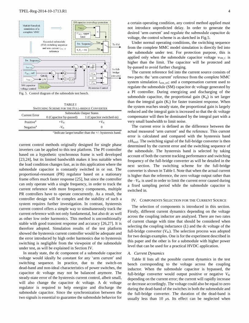
voltage, the control scheme is as sketched in Fig.5.
Under normal operating conditions, the switching sequence
from the complete MMC model simulation is directly fed into
the submodule under test. For protection purpose, this is
applied only when the submodule capacitor voltage vSM_C is
higher than the limit. The capacitor will be protected and
by-passed to avoid further charging.
The current reference fed into the current source consists of
two parts: the ‘arm current’ reference from the complete MMC
system simulation iarm_ref; and a compensation current used to
regulate the submodule (SM) capacitor dc voltage generated by
a PI controller. During energizing and discharging of the
submodule capacitor, the proportional gain (Kp) is set larger
than the integral gain (Ki) for faster transient response. When
the system reaches steady state, the proportional gain is largely
reduced and the integral gain is increased so that the dc voltage
compensator will then be dominated by the integral part with a
very small bandwidth to limit noise.
The current error is defined as the difference between the
actual measured ‘arm current’ and the reference. This current
error is calculated and compared with the hysteresis band
±Hband. The switching signal of the full-bridge converter is then
determined by the current error and the switching sequence of
the submodule. The hysteresis band is selected by taking
account of both the current tracking performance and switching
frequency of the full-bridge converter as will be detailed in the
next section. The switching scheme for the full-bridge
converter is shown in Table I. Note that when the actual current
is higher than the reference, the zero voltage output rather than
the –Vdc is used in order to limit the current error caused during
a fixed sampling period while the submodule capacitor is
switched in.
IV. COMPONENTS SELECTION FOR THE CURRENT SOURCE
The selection of components is introduced in this section.
Firstly, different current dynamics depending on the voltage
across the coupling inductor are analyzed. There are two rates
of current change with time that should be considered when
selecting the coupling inductance (L) and the dc voltage of the
full-bridge converter (Vdc). The selection process was adopted
for two design examples. One is for the experiment described in
this paper and the other is for a submodule with higher power
level that can be used for a practical HVDC application.
A. Current Dynamics
Table II lists all the possible current dynamics in the test
bench corresponding to the voltage across the coupling
inductor. When the submodule capacitor is bypassed, the
full-bridge converter would output positive or negative Vdc
depending on the current error; the current will rapidly increase
or decrease accordingly. The voltage could also be equal to zero
during the dead-band of the switches in both the submodule and
the full-bridge converter. The duration of the dead-band is
usually less than 10 μs. Its effect can be neglected when
Fig. 5. Control diagram of the submodule test bench.
TABLE I
SWITCHING SCHEME FOR THE FULL-BRIDGE CONVERTER
Current Error Submodule Output States
0 (Capacitor by-passed) 1 (Capacitor switched-in)
Positivea +Vdc +Vdc
Negativea -Vdc 0
a Indicate larger/smaller than the +/- hysteresis band.

TPEL-Reg-2014-10-1713.R1
5
compared with the switching frequency of the full-bridge
converter (around 5 kHz) and the submodule (250 Hz). When
the submodule capacitor is switched in and the current is above
its reference, the full-bridge controller could output –Vdc or zero
to reduce the current, however, the –Vdc output is not in use
because of the much larger error caused during a fixed
sampling period. Finally, when the current is below its
reference while the submodule capacitor is switched in, the
current will slowly increase since the voltage on the inductor is
only the difference between the dc source voltage of the
full-bridge converter and the submodule capacitor voltage.
B. Components Selection
Taking into account the variation of the ‘arm current’
reference, the rate of change of the current error between the
actual current and its reference can be categorized into fast and
slow groups as shown in Fig.6 (region 1-2: fast and region 3:
slow). ±Δimax is the permitted current error, ±Hband is the
hysteresis band, dimax is the error between the two values and
ΔT is the sampling period. The selection of the inductance and
the dc source voltage of the full-bridge converter must take
both change rates into consideration.
As region 2 in Fig.6 shows, the largest current error is most
likely to occur when it changes at the fastest rate. With a limited
sampling frequency, the current error will be much larger than
the set hysteresis band ±Hband. The selection of the hysteresis
band is then based on the permitted current error ±Δimax. One
way to determine the permitted current error is according to the
resulting error in the experiment outputs such as losses in the
power switches. In this test platform, the conduction losses of
the submodule IGBT and diode dominate since their switching
frequency is relatively low. Here is one way to estimate the
error in the conduction losses introduced by the current ripple
due to hysteresis switching. If the device’s on-state voltage is
simplified as a linear model, i.e. (V0+RI0), where V0 stands for
the IGBT/diode junction voltage, R is a fixed on-state
resistance of the IGBT/diode and I0 is the device current
(simplified as a constant firstly), the average conduction loss
for one device over a period of time T can be estimated as:
2
con 0 0 0 0 0 0 00
1( 0)
T
P I V RI dt V I RI IT
. (1)
If the high frequency ripple around the local current I0 is
expressed as a single component Iesin(ωet+φ), the average
conduction loss over the same period (T is much longer than
2π/ωe) is then:
con 0 e e 0 0 e e0
22 e
0 0 0
1sin sin
2
T
P I I t V R I I t dtT
RII V RI
(2)
(RI2e/2) is the error of the conduction loss introduced by the
high frequency current ripple. In practice, the device current I0
is not constant and the relative error varies with the magnitude
of the current. A relatively accurate estimation of the error can
be obtained by integrating (2) over the device’s conduction
time. For simplicity, as an example, a rough estimation is
applied here. For the IGBT/diode in this paper, as to be listed
later in Table IV, the value of V0 is around 20 times of RI0. The
current I0 uses the dc bias value as the average, i.e. 3.1A. If the
permitted current error is set to ±1.1A which is ±10% of the
peak ‘arm current’, Ie equals 1.1A and the introduced error in
the overall conduction losses is estimated to be around 1%.
Once the permitted current error is chosen, in order to
consider the additional error due to the limited sampling
frequency fs, the hysteresis band ±Hband is set within ±Δimax. The
gap between the two bands, referred as dimax is the maximum
current change in one sampling period ΔT, which can be
estimated by
max dc
1di V T A T
L , (3)
where L is the inductance, ω the MMC ac side line frequency
and A the peak amplitude of the ac component at the
fundamental frequency in the ‘arm current’. Here, in estimation
the harmonic circulating current components are neglected
because of their much lower amplitudes.
In order to ensure that the switching frequency of the
full-bridge converter is always lower than its upper limit fsw_max
for heat dissipation and EMC reasons, the hysteresis band is
decided according to the ratio between the two frequencies, i.e.
fs and fsw_max. When the sampling frequency is lower than twice
fsw_max, the hysteresis band can be set to zero. The full-bridge
converter may switch at every sampling instant as shown in
Fig.6 region 1. When the sampling frequency is higher than
twice fsw_max and lower than 4 times of fsw_max, the whole width
of the hysteresis band (2Hband) has to be set slightly larger than
the dimax. The possible maximum switching frequency of the
Fig. 6. Different types of current error dynamics.
TABLE II
DIFFERENT VOLTAGES ON THE COUPLING INDUCTOR
Full-bridge Converter
Output
Submodule Output
0 vSM_C
Voltage across the Coupling Inductor
-Vdc -Vdc -Vdc - vSM_C (Not in use)
0 0 (only during deadbands) -vSM_C
+Vdc +Vdc Vdc - vSM_C

TPEL-Reg-2014-10-1713.R1
6
full-bridge converter then reduces to a quarter of the sampling
frequency. As the ratio between the two frequencies further
increases, the hysteresis band is set according to the equation
below:
s maxmax s sw_max
sw_max
sband
sw_max
s sw_max
1, 2
22 21
2
0, 0 2
f idi f f
f
fH
f
f f
(4)
The above equation helps to divide the space between the
permitted current error ±Δimax into a multiple of dimax. The
selection of the inductance and the dc source voltage of the
full-bridge converter must satisfy the following equation:
dc max s
s
sw_max
2
22
V i fA
L f
f
. (5)
Besides (5), as stated above, the rising speed of the
controlled ‘arm current’ should be faster than its reference at
any time. With the harmonic components neglected, the fastest
rising speed of the reference is when the current crosses its dc
average from underneath. At that instant, the slope equals to
ωA. The slowest rising speed of the ‘arm current’ corresponds
to the smallest voltage drop on the inductor at that instant. Thus,
(6) should also be satisfied
dc SM_CV v
AL
. (6)
C. Design Examples
In the experimental set-up, the submodule rated dc voltage is
200 V and the ‘arm current’ would contain a 3.1 A dc
component plus a fundamental frequency sinusoidal
component with a peak amplitude of 8 A and other harmonics
with lower amplitudes. The allowed current error ±Δimax is set
at ±10% of the current peak or 1.1 A. The maximum optimal
switching frequency fsw_max of the IGBT power module in the
full-bridge converter is set at 6 kHz. The sampling frequency of
the dSpace DS1103 platform fs is 20 kHz. The hysteresis band
is thus ±0.37 A and according to (5), the possible Vdc for a few
inductance values L0 is derived and listed in the first two
columns in Table III.
The next step is to ensure that the slowest rising speed of the
controlled current is faster than its reference at the fastest point.
As shown in the submodule capacitor voltage waveform given
by computer simulation of the complete model (dashed blue
line in Fig.10 to be described later), vSM_C is around 175V when
the rising speed of the ‘arm current’ reaches its maximum.
According to (6), the corresponding voltages and the maximum
inductance values are derived and given in the last two columns
in Table III. Theoretically, parameters as in No.3 and No.4
groups are all suitable since the maximum allowed inductance
Lmax is larger than the value L0 (Equation (5)). The No.3 group
with lower inductance and dc source voltage requirements is
already sufficient to test the aforementioned submodule and is
thus chosen if higher test capacity is unnecessary. After the
ranges for the two parameters are decided, simulation work can
further help to get the optimal values.
The second design example estimates the required
inductance and dc source voltage of the full-bridge converter
for testing a submodule rated at 1000 Vdc with peak arm current
of 1000 A. The amplitude of the fundamental frequency
component in the arm current is estimated to be 700 A. The
allowed current error is set to ±5% of the peak arm current. If
the full-bridge converter is also based on an IGBT module with
5 kHz maximum optimal switching frequency (with a sampling
frequency of 50 kHz) the inductance and dc source voltage is
found to be around 4 mH and 1900 V respectively. If the
permitted current error can be widened to ±10%, the
corresponding inductance and dc source voltage are reduced to
1 mH and 1200 V.
According to the two design examples described above, the
dc source voltage of the full-bridge converter is around 20% to
100% higher than that of the submodule to be tested depending
on the required current tracking accuracy while the current
capacity should be the same as the current demand of the
submodule under test. With a much higher switching
frequency, the cooling system requirements of the full-bridge
converter will be higher than that of the submodule to be tested.
For testing submodules with reduced capacity as shown in this
paper, the increased voltage level as well as larger cooling
system is not a problem. For submodules with rated dc voltages
lower than 2 kV (with 3.3 kV IGBT/diode module), the device
modules with higher voltage levels (4.5 kV or 6.5 kV) are still
commercially available for the full-bridge converter. If the
submodule rated dc voltage is higher than 2 kV, series
connection of IGBTs/diodes in the full-bridge converter may
have to be used or other multilevel converters can be adopted to
replace the full-bridge. The cost of building this versatile test
platform may not be low (when compared with the cost of a
submodule) however it is believed that this one-off investment
can be justified by facilitating the design of an entire MMC
system.
V. SIMULATION AND EXPERIMENTAL VALIDATION OF THE
MODEL ASSISTED SUBMODULE TESTING SCHEME
This section demonstrates the effectiveness and accuracy of
the model assisted submodule testing scheme through both
TABLE III
POSSIBLE VALUES FOR DC SOURCE VOLTAGE AND INDUCTANCE
No. Equation (5) Equation (6)
L0 Vdc Vdc – VSM_C Lmax
1 15 mH 182 V 7 V 2.8 mH
2 18 mH 219 V 44 V 17.5 mH
3 20 mH 243 V 68 V 27 mH
4 25 mH 304 V 129 V 51 mH

TPEL-Reg-2014-10-1713.R1
7
computer simulation and experiment. In the time-domain
simulation, a complete MMC model and a test bench model
was built in Matlab/Simulink. Simulation results validated the
design of the submodule capacitor dc voltage regulator. The
power loss simulation showed the testing method to be an
effective and accurate way for the submodule electro-thermal
behavior analysis. In the experiment, both of the actual ‘arm
current’ and the submodule voltage agreed well with the
simulation results from the complete MMC model. At the end,
the current tracking error is analyzed.
A. Simulation Validation
A hypothetic, 21-level, 38 kVA grid-connected MMC with
half-bridge submodules is modelled in Matlab/Simulink. The
converter is connected to a ±2 kV dc-link and a 2.2 kV
(line-to-line rms), 50 Hz grid busbar through a three-phase
transformer. The arm inductor is 0.2p.u. All p.u. values are
based on ac side voltage and current. There are 20 submodules
in each arm with a 200 V rated submodule dc voltage. In the
simulation, the conduction losses of both IGBT and diode, the
switch-on and switch-off losses of IGBT and the diode reverse
recovery loss are derived by (7) and (8) respectively
2
1, ( , )
t
con k j k kt
E v i Temperature i dt (7)
1 2
,
( , )
( , )swtot p p k
t t
E E i Temperature , (8)
where k can be T for IGBT or D for diode; vj is the device’s
voltage drop (vCE for IGBT or vF for diode in the on state); Ep
can be ETswOn, ETswOff or EDrec representing IGBT switch-on loss,
IGBT switch-off loss and diode reverse recovery loss
respectively. Eswtot,p is the total loss for each kind in a given
period. Both vj and Ep are current and temperature dependent.
Based on the datasheet [28], IGBT/diode data for 125oC are
used for loss simulation. vj and Ep are expressed as
( )j k j k jv i a i b (9)
( )p k p kE i c i . (10)
All the system parameters are summarized in Table IV. A
model for the test bench is also built for simulation. The
parameters are listed in Table V. According to the components
selection process, the dc voltage for the full-bridge converter is
set to 240 V and the coupling inductor is chosen as 20 mH.
Submodule parameters are the same as those in the complete
MMC model. In steady state when the converter operates as a
rectifier absorbing 38 kW active power from the grid with unity
power factor, signals with a duration of one second of both arm
current and switching sequence of one submodule in the upper
arm of phase A in the complete MMC model are recorded and
then used to run the test bench model.
Fig.7 gives the simulation results during the start process. In
Fig.7 (a) the red line (starting from zero) represents the
submodule capacitor voltage in the test bench simulation. It
ramps up according to a linear reference from 0 to 200 V in 0.25
s. After that, the capacitor dc voltage remains constant and the
instantaneous voltage, as shown in the zoomed view, agrees
well with the results from the complete model simulation
sketched in the blue line. Fig.7 (b) compares the currents from
both simulations. The current generated by the full-bridge
converter model closely tracks the reference given by the
complete simulation, as is also shown in the zoomed view. The
dc bias with a magnitude of 3.1 A can be clearly seen. The
bottom graph is the compensation current generated by the PI
controller to regulate the dc component in the capacitor voltage.
From 0 – 0.25 s, Kp and Ki are set to 0.03 A/V and 0.01 A/(V.s)
TABLE IV
COMPLETE MMC SYSTEM PARAMETERS FOR SIMULATION
Item Value
dc-link voltage Grid voltage
Rated capacity
Transformer inductance Number of submodules
Arm inductance
Submodule rated dc voltage Submodule capacitance
4kV (pole-pole) 2.2kV line-to-line (rms), 50Hz
38kVA
0.1p.u. 20 per arm
0.2p.u.
200V 373.3μF
IGBT/Diode module
aT/bT
aD/bD
cTswOn
cTswOff
cDrec
Infineon IKW30N60T
0.0394(V/A)/0.666(V) 0.025(V/A)/0.75(V)
0.0175mJ/A per switch
0.04mJ/A per switch 0.0175mJ/A per switch
TABLE V
PARAMETERS FOR THE TEST BENCH MODEL
Item Value
dc source supply voltage
Coupling inductance
240V
20mH
Fig. 7. Simulation results comparison between the complete and the test bench models during start process: (a) submodule capacitor voltage, (b) arm current
and (c) current compensation.

TPEL-Reg-2014-10-1713.R1
8
respectively to charge the submodule capacitor. After the
capacitor dc voltage reaches the reference (200 V), Kp drops
down to 0.003 A/V with Ki rising slightly up to 0.02 A/(V.s).
The significantly reduced bandwidth of the PI controller helps
to limit the noise from the filter of the capacitor voltage. In
steady state, the compensation current is around 0.15 Adc which
is thought to make up for the impact of the current tracking
error of the hysteresis control on the submodule capacitor
voltage. This is based on the fact that the dc component of the
submodule capacitor voltage will immediately drop when the
voltage regulator is deactivated.
Table VI presents the power loss simulation results obtained
from both the complete system and the test bench models.
During the given period of time, the average power losses for
submodule switches given by the test bench model are very
close to those given by the complete model and the errors
around 1.5% agree with the error estimation given in Section
IV.B. The error in the conduction loss of the lower IGBT T2 is
larger than the others. The reason can be explained by bottom
graph in Fig.2 as the conduction time of T2 is short and the
current passing through it is small when the converter rectifies
active power. Also, the conduction loss error of the lower diode
D2 is minus rather than plus, which is due to the +0.15A
compensation current.
B. Experiment Results
Fig.8 shows the prototype assembled and installed in a
protected enclosure for the validation of the proposed
submodule testing scheme with all the parameters detailed in
Table VII. Fig.9 shows an oscilloscope snapshot of the
experimental results. From top to bottom are the waveforms for
the submodule capacitor voltage (red), submodule switching
sequence (blue) and the actual ‘arm current’ (yellow). The
average capacitor voltage over a period is measured to be
around the set 200 V reference. A dc bias can be clearly seen in
the actual ‘arm current’.
Fig.10 compares the results from the experiment (solid red)
and the simulation of the complete MMC model (dashed blue).
Fig.10 (a) shows that the submodule capacitor voltage in the
experiment agrees well with the result given by the complete
model simulation. In Fig.10 (b), the current flowing into the
submodule in the experiment tightly tracks the given reference.
The two zoomed views give the details of the actual ‘arm
current’ achieved by the hysteresis control in the full-bridge
converter. The zoomed view on the right side shows that even
with the slowest rising speed, the actual current is still capable
of tracking the reference at its fastest-rising instant, which
verifies the components selection process provided in Section
IV.B. The difference between the actual current and the
reference are shown in Fig.10 (c). The current errors are all
within the designed ±1.1 A region. Fig.10 (d) gives the details
of the switching process. The maximums current change in a
sampling period is found to be 0.82 A which is slightly larger
than the estimated 0.73 A according to (3). The error is
introduced by the compensation current which is used to
regulate the submodule capacitor dc voltage.
Fig.11 gives the FFT of the current error. The high order
harmonics around 1.6 kHz and 4 kHz are due to the hysteresis
switching. Their impacts have been shown to be limited on the
electro-thermal performance of the submodule under test. As
TABLE VI
SUBMODULE SEMICONDUCTOR DEVICES LOSSES COMPARISON BETWEEN THE
COMPLETE MODEL AND THE TEST BENCH MODEL – RECTIFYING OPERATION,
10 A LINE CURRENT
Losses (W)
Complete
model
Test bench
model
Complete
model
Test bench
model
Upper module (T1/D1) Lower module (T2/D2)
IGBT
conduction 0.967
0.980
(+1.3%) 0.152
0.158
(+4%)
IGBT switch-on
0.019 0.018 0.005 0.005
IGBT
switch-off 0.042 0.041 0.011 0.012
Diode
conduction 0.865
0.878
(+1.5%) 3.233
3.180
(-1.6%)
Diode rev. recovery
0.005 0.005 0.018 0.018
Sub-total
(difference) 1.896
1.922
(+1.4%) 3.420
3.373
(-1.4%)
TABLE VII
PARAMETERS FOR THE EXPERIMENT
Item Value
dc source supply voltage
Coupling inductor Submodule rated dc voltage
240V
20mH @ 20Adc 200V
Submodule capacitance
Submodule IGBT/diode module Interface
Temperature recorder
373.3μF from EPCOS
Infineon IKW30N60T dSpace DS1103
TC-8 thermocouple data logger
Fig. 8. Submodule test bench installed in a protected enclosure.

TPEL-Reg-2014-10-1713.R1
9
shown in the zoomed view, the biggest error is found at the
fundamental frequency 50 Hz, which is caused by the phase
delay between the actual ‘arm current’ and its reference. The
delay angle is 0.8o within which 0.45o is due to the 20 kHz
sampling frequency. 0.3o is introduced by the RC filter in the
current sensor and the rest is caused by the hysteresis control
itself. The phase delay also causes the error at 100 Hz
corresponding to the major circulating current component in
the ‘arm current’. Besides that, as discussed in the simulation
results, the dc error is introduced by current compensation. The
amplitudes of the above errors are small when compared with
the peak ‘arm current’. If those errors are not acceptable in
certain applications, methods such as narrower permitted
current error band, faster sampling frequency and/or variable
hysteresis band could be adopted.
VI. APPLICATION: ELECTRO-THERMAL BEHAVIOR TEST
Two sets of electro-thermal behavior tests are shown as a
demonstration of the proposed submodule testing method. One
test compares the temperature of two submodules at different
locations in the same MMC converter. The other test compares
the temperature of the same submodule when the MMC
converter operates in four different conditions.
A. Electro-thermal Test 1
In the first test, the arm current references and switching
sequences of two submodules at different locations in the same
MMC converter are recorded by complete model simulation.
The converter operates as a rectifier absorbing 38kW active
power from the ac grid as in Section V. In the test, the
recordings are run repeatedly for 2500 seconds for both
submodules. The temperatures of the upper switch, lower
switch and the ambient are recorded and shown in Fig.12. The
results agree well with the loss simulations (Table VI) which
show that during rectification, most of the arm current would
pass through the diode in the lower switch and thus leads to
higher temperature than the upper pair.
According to Fig.12, the temperatures of submodules at
different locations are similar when the converter system is well
balanced. As shown in the top graph in Fig.12, for submodule
No. 1 in the upper arm in phase A, the absolute temperature rise
above the ambient for the upper switch is 8.73 oC and that for
Fig. 9. Experiment results recorded by the oscilloscope. Horizontal Axis: 10ms/div. Channel 1-‘arm current’: 5A/div, -1.5div offset (yellow). Channel
2-submodule capacitor voltage: 50V/div, -1.5div offset (red). Channel
3-submodule switching sequence (blue).
Fig. 10. Comparison between the experiment results (solid red) and the complete model simulation (dashed blue): (a) submodule capacitor voltage; (b)
‘arm current’; (c) current error; (d) zoomed view of the current error.
Fig. 11. Top: FFT of the current error; bottom: zoomed view.
TPEL-Reg-2014-10-1713.R1
10
the lower switch is 14.97 oC. As the bottom graph shows, for
submodule No. 10 in the lower arm in phase B, the temperature
rise for the upper switch is 8.74 oC and that for the lower switch
is 15.63 oC. Loss simulations show that during the recorded 1
second period, the average power losses for the upper switch of
the first submodule is 1.95 W and that for its lower switch is
3.38 W. The average power loss for the upper switch of the
second submodule is 1.92 W and that for its lower switch is
3.43 W. Although the limited experiment time did not allow the
temperature of both submodules to reach steady state, the
already derived experiment results again agree well with the
simulation. The results above further demonstrate the accuracy
of the test bench in electro-thermal analysis.
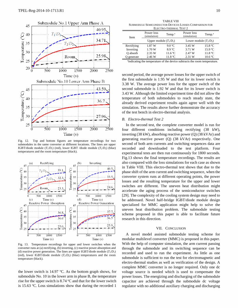
B. Electro-thermal Test 2
In the second test, the complete converter model is run for
four different conditions including rectifying (38 kW),
inverting (38 kW), absorbing reactive power (Q) (38 kVAr) and
generating reactive power (Q) (38 kVAr) respectively. One
second of both arm currents and switching sequences data are
recorded and downloaded to the test platform. Four
experimental tests are then run continuously for 1800 seconds.
Fig.13 shows the final temperature recordings. The results are
also compared with the loss simulations for each case as shown
in Table VIII. This electro-thermal test shows that due to the
phase shift of the arm current and switching sequence, when the
converter system runs at different operating points, the power
losses and the resulting temperature for the upper and lower
switches are different. The uneven heat distribution might
accelerate the aging process of the semiconductor switches
[29]. The complexity of the cooling system design may need to
be addressed. Novel half-bridge IGBT/diode module design
specialized for MMC application might help to solve the
uneven heat distribution problem. The submodule testing
scheme proposed in this paper is able to facilitate future
research in this direction.
VII. CONCLUSION
A novel model assisted submodule testing scheme for
modular multilevel converter (MMC) is proposed in this paper.
With the help of computer simulation, the arm current passing
through the submodule and its switching sequence can be
recorded and used to run the experiment. As little as one
submodule is sufficient to run the test for electromagnetic and
electro-thermal studies as well as verification of the design. A
complete MMC converter is no longer required. Only one dc
voltage source is needed which is used to compensate the
power losses. The energizing and discharging of the submodule
capacitor are achieved through the submodule dc voltage
regulator with no additional auxiliary charging and discharging
TABLE VIII
SUBMODULE SEMICONDUCTOR DEVICES LOSSES COMPARISON FOR
ELECTRO-THERMAL TEST 2
Item
Power loss (simulation)
Temp.a Power loss (simulation)
Temp.a
Upper module (T1/D1) Lower module (T2/D2)
Rectifying 1.87 W 9.0 oC 3.45 W 15.8 oC
Inverting 1.70 W 8.9 oC 3.71 W 15.9 oC
Q absorb 2.35 W 11.6 oC 2.47 W 11.8 oC
Q generate 2.46 W 11.8 oC 2.31 W 10.6 oC aindicating the temperature of the device subtracts the room temperature.
Fig. 12. Top and bottom figures are temperature recordings for two
submodules in the same converter at different locations. The lines are upper
IGBT/diode module (T1/D1) (red), lower IGBT /diode module (T2/D2) (blue) temperatures and the room temperature (black).
Fig. 13. Temperature recordings for upper and lower switches when the converter runs at (a) rectifying, (b) inverting, (c) reactive power absorption and
(d) reactive power generation. The lines are upper IGBT/diode module (T1/D1)
(red), lower IGBT/diode module (T2/D2) (blue) temperatures and the room temperature (black).

TPEL-Reg-2014-10-1713.R1
11
circuits.
During the test, the ‘arm current’ can be faithfully achieved,
which contains not only the fundamental frequency component
but also the dc bias and the harmonic circulating current
components. Both simulations and experiments showed the
validity and accuracy of the proposed testing scheme. The
synchronization between the ‘arm current’ and the submodule
switching sequence is shown to be adequate. This testing
method is proven to be capable of facilitating research such as
submodule thermal stability test, optimal cooling system design,
optimal switching pattern algorithm, novel submodule structure
design as well as reliability testing. It is intended to fill the gap
between computer simulation and the complete converter
experiment in the physics domain.
REFERENCES
[1] S. Rohner, S. Bernet, M. Hiller, and R. Sommer, "Modulation, losses, and semiconductor requirements of modular multilevel converters," IEEE
Trans. Ind. Electron., vol. 57, no. 8, pp. 2633-2642, Aug. 2010.
[2] Q. Tu, Z. Xu, and L. Xu, "Reduced switching-frequency modulation and circulating current suppression for modular multilevel converters," IEEE
Trans. Power Del., vol. 26, no. 3, pp. 2009-2017, Jul. 2011.
[3] A. Lesnicar and R. Marquardt, "An innovative modular multilevel converter topology suitable for a wide power range," in Proc. IEEE
Bologna Power Tech, Jun. 2003, vol. 3, p. 6.
[4] A. Nami, J. Liang, F. Dijkhuizen, and G.D. Demetriades, “Modular multilevel converters for HVDC applications: review on converter cells
and functionalities,” IEEE Trans. Power Electron., vol. 30, no. 1, pp.
18-36, Jan. 2015. [5] S. Debnath, J. Qin, B. Bahrani, M. Saeedifard, and P. Barbosa,
“Operation, control, and applications of the modular multilevel converter:
a review,” IEEE Trans. Power Electron., vol. 30, no. 1, pp. 37-53, Jan. 2015.
[6] M. Glinka, "Prototype of multiphase modular-multilevel-converter with 2
MW power rating and 17-level-output-voltage," in Proc. Conf. Rec. IEEE
PESC, 2004, vol.4, pp. 2572–2576.
[7] Q. Song, W. Liu, Z. Li, H. Rao, S. Xu, and L. Li, “A steady-state analysis
method for a modular multilevel converter,” IEEE Trans. Power Electron., vol. 28, no. 8, pp. 3702-3713, Aug. 2013.
[8] K. Ilves, L. Harnefors, S. Norrga, and H.-P. Nee, “Analysis and operation
of modular multilevel converters with phase-shifted carrier PWM,” IEEE Trans. Power Electron., vol. 30, no. 1, pp. 268-283, Jan. 2015.
[9] M. Hagiwara and H. Akagi, "Control and experiment of
pulsewidth-modulated modular multilevel converters," IEEE Trans. Power Electronics, vol. 24, no. 7, pp. 1737-1746, Jul. 2009.
[10] K. Ilves, L. Harnefors, S. Norrga, and H.-P. Nee, “Predictive sorting
algorithm for modular multilevel converters minimizing the spread in the submodule capacitor voltages,” IEEE Trans. Power Electron., vol. 30, no.
1, pp. 440-449, Jan. 2015.
[11] D. Siemaszko, “Fast sorting method for balancing capacitor voltages in modular multilevel converters,” IEEE Trans. Power Electron., vol. 30, no.
1, pp. 463-470, Jan. 2015.
[12] X. Yang, J. Li, X. Wang, W. Fan, and T. Q. Zheng, "Circulating current model of modular multilevel converter," in Proc. APPEEC, 2011, pp. 1-6.
[13] L. Harnefors, A. Antonopoulos, S. Norrga, L. Angquist, and H. P. Nee,
"Dynamic analysis of modular multilevel converters," IEEE Trans. Ind. Electron., vol. 60, no. 7, pp. 2526-2537, Jul. 2013.
[14] Z. Li, P. Wang, Z. Chu, H. Zhu, Y. Luo, and Y. Li, “An inner current
suppressing method for modular multilevel converters,” IEEE Trans. Power Electron., vol. 28, no. 11, pp. 4873-4879, Nov. 2013.
[15] L. He, K. Zhang, J. Xiong, and S. Fan, “A repetitive control scheme for harmonic suppression of circulating current in modular multilevel
converters,” IEEE Trans. Power Electron., vol. 30, no. 1, pp. 471-481,
Jan. 2015. [16] J. Xu, C. Zhao, W. Liu, and C. Guo, "Accelerated model of modular
multilevel converters in PSCAD/EMTDC," IEEE Trans. Power Del., vol.
28, no. 1, pp. 129-136, Jan. 2013. [17] C. Gao, X. Luo, X. Wei, and Z. Lv, “Steady-state operation test device of
flexible direct current transmission MMC high-pressure submodule,”
China Patent CN201993425U, Sep. 28, 2011.
[18] G. Tang, K. Zha, C. Gao, X. Luo, and Y. Yang, “Steady-state operation test method for flexible direct-current power transmission modular
multilevel converter (MMC) high-voltage sub-module,” China Patent
CN102175942(B), Jul. 2, 2014. [19] P. Wang and Z. Chu, “Test device and test method for modularized
multi-level current transformer sub-module,” China Patent
CN103018586A, Apr. 3, 2013. [20] J. Feng, J. Ke, W. Deng, Z. Lv, and D. Liu, “Flexible direct current
transmission sub-module test device and test method,” China Patent
CN103063945A, Apr. 24, 2013. [21] T. Modeer, S. Norrga, and H. P. Nee, "Resonant test circuit for
high-power cascaded converter submodules," in Proc. 15th Eur. Conf.
Power Electron. Appl., 2013, pp. 1–5. [22] E. Solas, G. Abad, J. A. Barrena, S. Aurtenetxea, A. Carcar, and L. Zajac,
"Modular multilevel converter with different submodule concepts Part II:
experimental validation and comparison for HVDC application," IEEE Trans. Ind. Electron., vol. 60, no.10, pp. 4536-4545, Oct. 2013.
[23] U. A. Miranda, L. G. B. Rolim, and M. Aredes, “A DQ synchronous
reference frame current control for single-phase converters,” in Proc. 36th IEEE PESC, 2005, pp. 1377-1381.
[24] B. Bahrani, A. Rufer, S. Kenzelmann, and L. Lopes, “Vector control of
single-phase voltage-source converters based on fictive-axis emulation,” IEEE Trans. Ind. Appl., vol. 47, no. 2, pp. 831-840, Mar./Apr. 2011.
[25] D. N. Zmood and D. G. Holmes, “Stationary frame current regulation of
PWM inverters with zero steady-state error,” IEEE Trans. Power Electron., vol. 18, no. 3, pp. 814-822, May 2003.
[26] H. Mao, X. Yang, Z. Chen, and Z. Wang, “A hysteresis current controller for single-phase three-level voltage source inverters,” IEEE Trans. Power
Electron., vol. 27, no. 7, pp. 3330-3339, Jul. 2012.
[27] K. M. Rahman, M. R. Khan, M. A. Choudhury, and M. A. Rahman, "Variable-band hysteresis current controllers for PWM voltage-source
inverters," IEEE Trans. Power Electron., vol. 12, no. 6, pp. 964-970, Nov.
1997. [28] Infineon IKW30N60T. (2013) [Online]. Available:
http://www.infineon.com/dgdl/Infineon-IKW30N60T-DS-v02_05-en.pd
f?fileId=db3a304412b4079501 12b42889a63e1d [29] D. Xiang, L. Ran, P. Tavner, S. Yang, A. Bryant, and P. Mawby,
"Condition monitoring power module solder fatigue using inverter
harmonic identification," IEEE Trans. Power Electron., vol. 27, no. 1, pp. 235-247, Jan. 2012.
Yuan Tang (S’14) received a B.Eng. degree in
electrical engineering from Huazhong University of Science and Technology, Wuhan, China and the
University of Birmingham, Birmingham, UK, in
2012. He is currently working toward a Ph.D. degree in the School of Engineering, the University of
Warwick, Coventry, UK.
He received a full scholarship from the School of
Engineering, the University of Warwick. He also
participated as a research assistant for a project on
offshore low frequency ac power transmission
funded by Scottish Power, UK. His research interests include modular
multilevel converters, ac/dc power conversions, renewable energy (solar and
wind) generation and integration.
Li Ran (M'98-SM'07) received a PhD degree in Power Systems Engineering from Chongqing
University, Chongqing, China, in 1989. He was a
Research Associate with the Universities of Aberdeen, Nottingham and Heriot-Watt, at
Aberdeen, Nottingham and Edinburgh in the UK
respectively. He became a Lecturer in Power Electronics with Northumbria University,
Newcastle upon Tyne, the UK in 1999 and was
seconded to Alstom Power Conversion, Kidsgrove, UK in 2001. Between 2003 and 2012, he was with
Durham University, UK. He joined the University
of Warwick, Coventry, UK as a Professor in Power Electronics - Systems in 2012. His research interests include the application of Power Electronics for
electric power generation, delivery and utilisation.

TPEL-Reg-2014-10-1713.R1
12
Olayiwola Alatise (M'05) received the B.Eng.
degree (with first-class honors) in electronic engineering and the Ph.D. degree in
microelectronics and semiconductors from
Newcastle University, U.K., in 2008. His research focused on mixed-signal performance
enhancements in strained Si/SiGe
metal–oxide–semiconductor field-effect transistors (MOSFETs). In June 2008, he joined the Innovation
R&D Department, NXP Semiconductors, as a
Development Engineer, where he designed, processed, and qualified discrete power trench MOSFETs for automotive applications and switched-mode power
supplies. In November 2010, he became a Science City Research Fellow with
the University of Warwick and since August 2012, he is serving as Associate professor of Electrical Engineering in University of Warwick, Coventry, U.K.
His research interest include investigating advanced power semiconductor
materials and devices for improved energy conversion efficiency.
Philip Mawby (S'85-M'86-SM'01) received the
B.Sc. and Ph.D. degrees in electronic and electrical engineering from the University of Leeds, U.K., in
1983 and 1987, respectively. His Ph.D. was focused
on GaAs/AlGaAs heterojunction bipolar transistors for high-power radio frequency applications at the
GEC Hirst Research Centre, Wembley, U.K.
In 2005, he joined the University of Warwick, Coventry, U.K., as the Chair of power electronics.
He was also with the University of Wales, Swansea, U.K. for 19 years and held the Royal Academy of
Engineering Chair for power electronics, where he established the Power
Electronics Design Center. He has been internationally recognized in the area of power electronics and power device research. He was also involved in the
development of device simulation algorithms, as well as optoelectronic and
quantum-based device structures. He has authored or coauthored more than 100 journal and conference papers. His current research interests include materials
for new power devices, modeling of power devices and circuits.
Prof. Mawby has been involved in many international conference committees, including the ISPSD, EPE, and the ESSDERC. He is a Chartered Engineer, a
Fellow of the IET, and a Fellow of the Institute Physics. He is a Distinguished
Lecturer for the IEEE Electron Devices Society.