Embed Size (px)
Citation preview
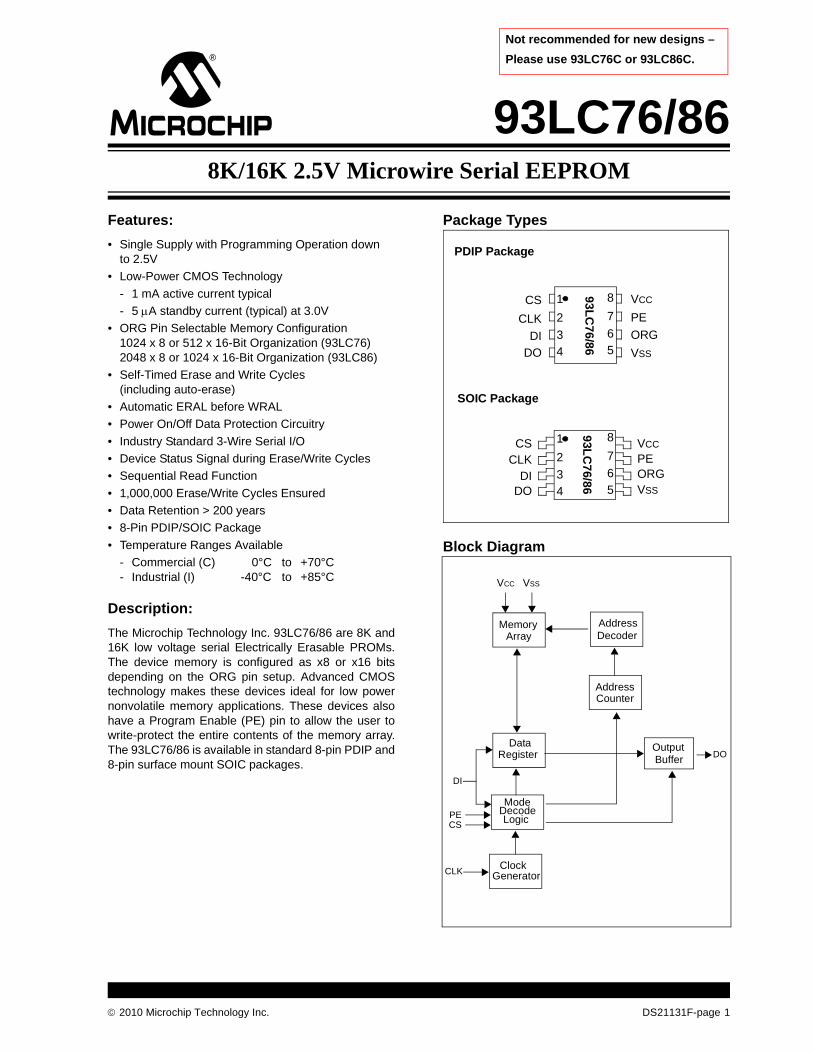
93LC76/868K/16K 2.5V Microwire Serial EEPROM
Not recommended for new designs –
Please use 93LC76C or 93LC86C.
Features:
• Single Supply with Programming Operation down to 2.5V
• Low-Power CMOS Technology
- 1 mA active current typical
- 5 A standby current (typical) at 3.0V
• ORG Pin Selectable Memory Configuration1024 x 8 or 512 x 16-Bit Organization (93LC76)2048 x 8 or 1024 x 16-Bit Organization (93LC86)
• Self-Timed Erase and Write Cycles(including auto-erase)
• Automatic ERAL before WRAL
• Power On/Off Data Protection Circuitry
• Industry Standard 3-Wire Serial I/O
• Device Status Signal during Erase/Write Cycles
• Sequential Read Function
• 1,000,000 Erase/Write Cycles Ensured
• Data Retention > 200 years
• 8-Pin PDIP/SOIC Package
• Temperature Ranges Available
Description:
The Microchip Technology Inc. 93LC76/86 are 8K and16K low voltage serial Electrically Erasable PROMs.The device memory is configured as x8 or x16 bitsdepending on the ORG pin setup. Advanced CMOStechnology makes these devices ideal for low powernonvolatile memory applications. These devices alsohave a Program Enable (PE) pin to allow the user towrite-protect the entire contents of the memory array.The 93LC76/86 is available in standard 8-pin PDIP and8-pin surface mount SOIC packages.
Package Types
Block Diagram- Commercial (C) 0°C to +70°C- Industrial (I) -40°C to +85°C
SOIC Package
PDIP Package
CS
CLK
DI
DO VSS
PE
VCC
ORG
CSCLK
DIDO
VCC
PEORGVSS
93L
C7
6/86
93
LC
76
/86
1
2
3
4
8
7
65
1
2
3
4
8
7
65
DO
CS
CLK
VCC VSS
MemoryArray
AddressDecoder
DataRegister
CounterAddress
OutputBuffer
ModeDecodeLogic
GeneratorClock
DI
PE
2010 Microchip Technology Inc. DS21131F-page 1
93LC76/86
1.0 ELECTRICAL CHARACTERISTICS
Absolute Maximum Ratings(†)
VCC.............................................................................................................................................................................7.0V
All inputs and outputs w.r.t. VSS ........................................................................................................ -0.6V to Vcc + 1.0V
Storage temperature ...............................................................................................................................-65°C to +150°C
Ambient temperature with power applied................................................................................................-40°C to +125°C
Soldering temperature of leads (10 seconds) .......................................................................................................+300°C
ESD protection on all pins ..........................................................................................................................................4 kV
1.1 AC Test Conditions
† NOTICE: Stresses above those listed under “Absolute Maximum Ratings” may cause permanent damage to thedevice. This is a stress rating only and functional operation of the device at these or any other conditions above thoseindicated in the operational listings of this specification is not implied. Exposure to Absolute Maximum Ratingconditions for extended periods may affect device reliability.
AC Waveform:
VLO = 2.0V
VHI = Vcc - 0.2V (Note 1)
VHI = 4.0V for (Note 2)
Timing Measurement Reference Level
Input 0.5 VCC
Output 0.5 VCC
Note 1: For VCC 4.0V
2: For VCC > 4.0V
DS21131F-page 2 2010 Microchip Technology Inc.
93LC76/86
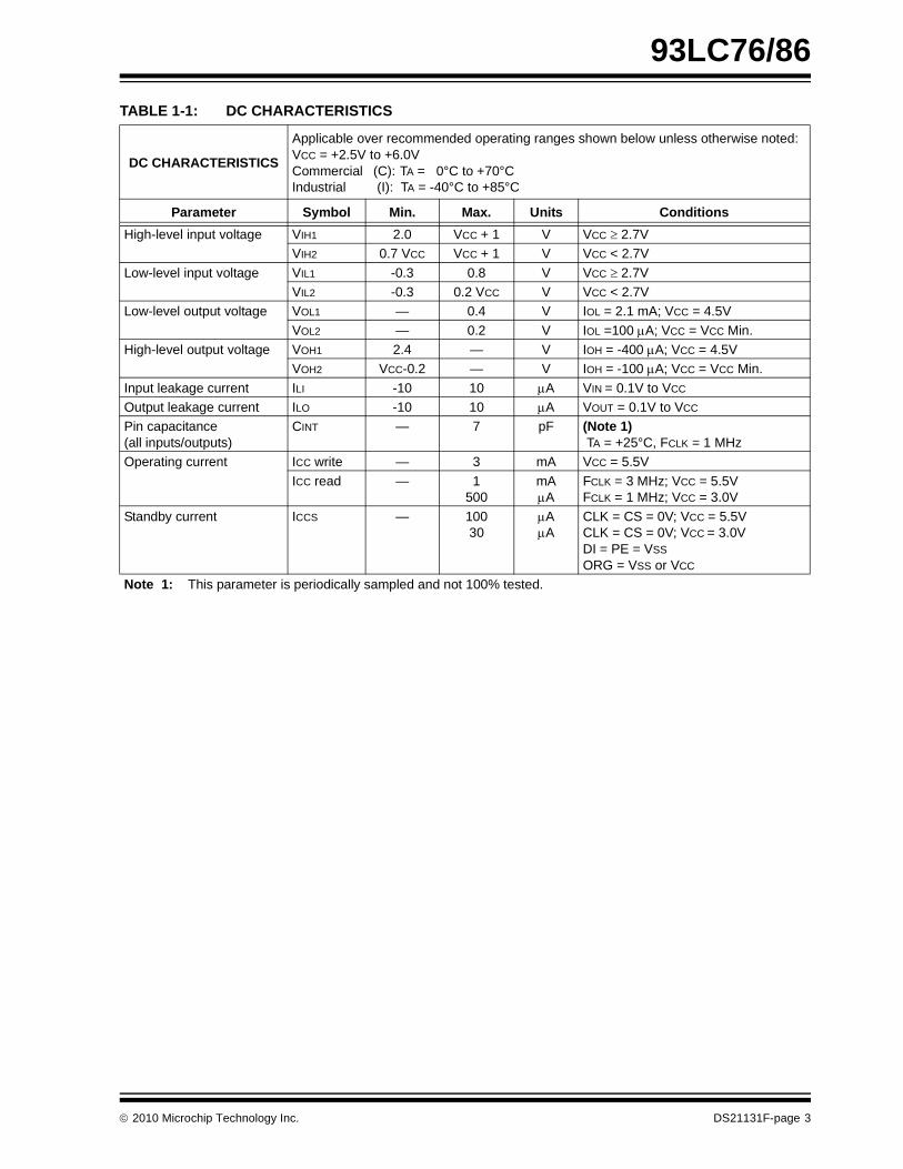
TABLE 1-1: DC CHARACTERISTICS
DC CHARACTERISTICS
Applicable over recommended operating ranges shown below unless otherwise noted:VCC = +2.5V to +6.0VCommercial (C): TA = 0°C to +70°CIndustrial (I): TA = -40°C to +85°C
Parameter Symbol Min. Max. Units Conditions
High-level input voltage VIH1 2.0 VCC + 1 V VCC 2.7V
VIH2 0.7 VCC VCC + 1 V VCC < 2.7V
Low-level input voltage VIL1 -0.3 0.8 V VCC 2.7V
VIL2 -0.3 0.2 VCC V VCC < 2.7V
Low-level output voltage VOL1 — 0.4 V IOL = 2.1 mA; VCC = 4.5V
VOL2 — 0.2 V IOL =100 A; VCC = VCC Min.
High-level output voltage VOH1 2.4 — V IOH = -400 A; VCC = 4.5V
VOH2 VCC-0.2 — V IOH = -100 A; VCC = VCC Min.
Input leakage current ILI -10 10 A VIN = 0.1V to VCC
Output leakage current ILO -10 10 A VOUT = 0.1V to VCC
Pin capacitance(all inputs/outputs)
CINT — 7 pF (Note 1) TA = +25°C, FCLK = 1 MHz
Operating current ICC write — 3 mA VCC = 5.5V
ICC read — 1 500
mAA
FCLK = 3 MHz; VCC = 5.5VFCLK = 1 MHz; VCC = 3.0V
Standby current ICCS — 10030
AA
CLK = CS = 0V; VCC = 5.5VCLK = CS = 0V; VCC = 3.0V DI = PE = VSS
ORG = VSS or VCC
Note 1: This parameter is periodically sampled and not 100% tested.
2010 Microchip Technology Inc. DS21131F-page 3
93LC76/86
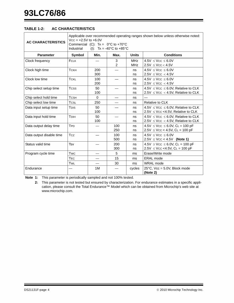
TABLE 1-2: AC CHARACTERISTICS
AC CHARACTERISTICS
Applicable over recommended operating ranges shown below unless otherwise noted:VCC = +2.5V to +6.0VCommercial (C): TA = 0°C to +70°CIndustrial (I): TA = -40°C to +85°C
Parameter Symbol Min. Max. Units Conditions
Clock frequency FCLK — 32
MHzMHz
4.5V VCC 6.0V2.5V VCC 4.5V
Clock high time TCKH 200300
— nsns
4.5V VCC 6.0V2.5V VCC 4.5V
Clock low time TCKL 100200
— nsns
4.5V VCC 6.0V2.5V VCC 4.5V
Chip select setup time TCSS 50100
— nsns
4.5V VCC 6.0V, Relative to CLK2.5V VCC 4.5V, Relative to CLK
Chip select hold time TCSH 0 — ns —
Chip select low time TCSL 250 — ns Relative to CLK
Data input setup time TDIS 50100
— nsns
4.5V VCC 6.0V, Relative to CLK2.5V VCC <4.5V, Relative to CLK
Data input hold time TDIH 50100
— nsns
4.5V VCC 6.0V, Relative to CLK2.5V VCC 4.5V, Relative to CLK
Data output delay time TPD — 100250
nsns
4.5V VCC 6.0V, CL = 100 pF2.5V VCC < 4.5V, CL = 100 pF
Data output disable time TCZ — 100500
nsns
4.5V VCC 6.0V2.5V VCC < 4.5V (Note 1)
Status valid time Tsv — 200300
nsns
4.5V VCC 6.0V, CL = 100 pF2.5V VCC <4.5V, CL = 100 pF
Program cycle time TWC — 5 ms Erase/Write mode
TEC — 15 ms ERAL mode
TWL — 30 ms WRAL mode
Endurance — 1M — cycles 25°C, Vcc = 5.0V, Block mode (Note 2)
Note 1: This parameter is periodically sampled and not 100% tested.
2: This parameter is not tested but ensured by characterization. For endurance estimates in a specific appli-cation, please consult the Total Endurance™ Model which can be obtained from Microchip’s web site at www.microchip.com.
DS21131F-page 4 2010 Microchip Technology Inc.
93LC76/86
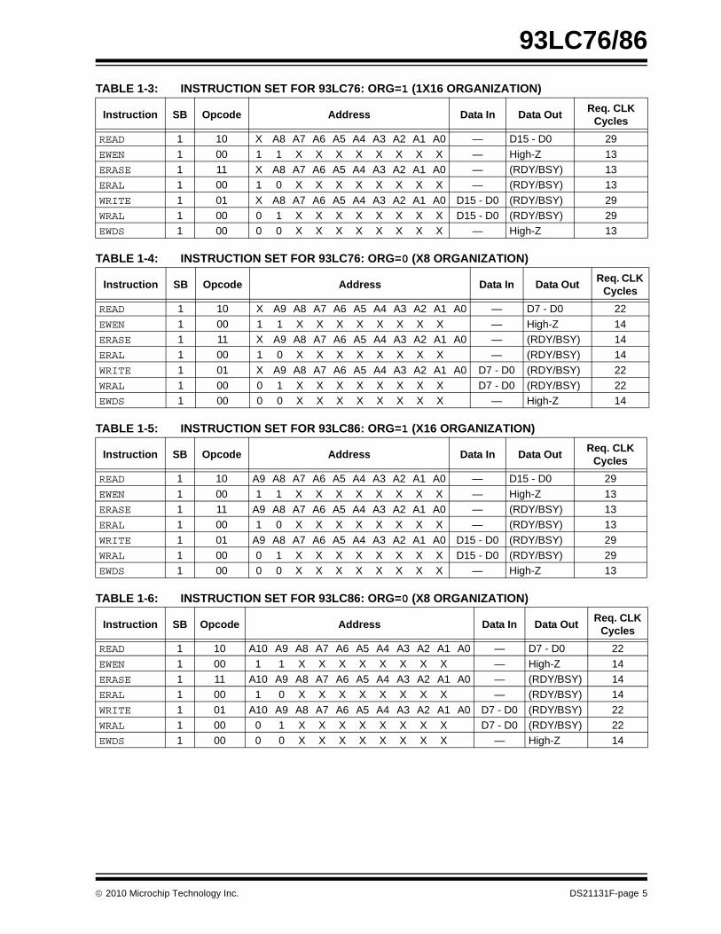
TABLE 1-3: INSTRUCTION SET FOR 93LC76: ORG=1 (1X16 ORGANIZATION)
TABLE 1-4: INSTRUCTION SET FOR 93LC76: ORG=0 (X8 ORGANIZATION)
TABLE 1-5: INSTRUCTION SET FOR 93LC86: ORG=1 (X16 ORGANIZATION)
TABLE 1-6: INSTRUCTION SET FOR 93LC86: ORG=0 (X8 ORGANIZATION)
Instruction SB Opcode Address Data In Data OutReq. CLK
Cycles
READ 1 10 X A8 A7 A6 A5 A4 A3 A2 A1 A0 — D15 - D0 29
EWEN 1 00 1 1 X X X X X X X X — High-Z 13
ERASE 1 11 X A8 A7 A6 A5 A4 A3 A2 A1 A0 — (RDY/BSY) 13
ERAL 1 00 1 0 X X X X X X X X — (RDY/BSY) 13
WRITE 1 01 X A8 A7 A6 A5 A4 A3 A2 A1 A0 D15 - D0 (RDY/BSY) 29
WRAL 1 00 0 1 X X X X X X X X D15 - D0 (RDY/BSY) 29
EWDS 1 00 0 0 X X X X X X X X — High-Z 13
Instruction SB Opcode Address Data In Data OutReq. CLK
Cycles
READ 1 10 X A9 A8 A7 A6 A5 A4 A3 A2 A1 A0 — D7 - D0 22
EWEN 1 00 1 1 X X X X X X X X — High-Z 14
ERASE 1 11 X A9 A8 A7 A6 A5 A4 A3 A2 A1 A0 — (RDY/BSY) 14
ERAL 1 00 1 0 X X X X X X X X — (RDY/BSY) 14
WRITE 1 01 X A9 A8 A7 A6 A5 A4 A3 A2 A1 A0 D7 - D0 (RDY/BSY) 22
WRAL 1 00 0 1 X X X X X X X X D7 - D0 (RDY/BSY) 22
EWDS 1 00 0 0 X X X X X X X X — High-Z 14
Instruction SB Opcode Address Data In Data OutReq. CLK
Cycles
READ 1 10 A9 A8 A7 A6 A5 A4 A3 A2 A1 A0 — D15 - D0 29
EWEN 1 00 1 1 X X X X X X X X — High-Z 13
ERASE 1 11 A9 A8 A7 A6 A5 A4 A3 A2 A1 A0 — (RDY/BSY) 13
ERAL 1 00 1 0 X X X X X X X X — (RDY/BSY) 13
WRITE 1 01 A9 A8 A7 A6 A5 A4 A3 A2 A1 A0 D15 - D0 (RDY/BSY) 29
WRAL 1 00 0 1 X X X X X X X X D15 - D0 (RDY/BSY) 29
EWDS 1 00 0 0 X X X X X X X X — High-Z 13
Instruction SB Opcode Address Data In Data OutReq. CLK
Cycles
READ 1 10 A10 A9 A8 A7 A6 A5 A4 A3 A2 A1 A0 — D7 - D0 22
EWEN 1 00 1 1 X X X X X X X X — High-Z 14
ERASE 1 11 A10 A9 A8 A7 A6 A5 A4 A3 A2 A1 A0 — (RDY/BSY) 14
ERAL 1 00 1 0 X X X X X X X X — (RDY/BSY) 14
WRITE 1 01 A10 A9 A8 A7 A6 A5 A4 A3 A2 A1 A0 D7 - D0 (RDY/BSY) 22
WRAL 1 00 0 1 X X X X X X X X D7 - D0 (RDY/BSY) 22
EWDS 1 00 0 0 X X X X X X X X — High-Z 14
2010 Microchip Technology Inc. DS21131F-page 5
93LC76/86
2.0 PRINCIPLES OF OPERATION
When the ORG pin is connected to VCC, the x16 orga-nization is selected. When it is connected to ground,the x8 organization is selected. Instructions, addressesand write data are clocked into the DI pin on the risingedge of the clock (CLK). The DO pin is normally held ina high-Z state except when reading data from thedevice, or when checking the Ready/Busy statusduring a programming operation. The Ready/Busystatus can be verified during an erase/write operationby polling the DO pin; DO low indicates that program-ming is still in progress, while DO high indicates thedevice is ready. The DO will enter the high-impedancestate on the falling edge of the CS.
2.1 Start Condition
The Start bit is detected by the device if CS and DI areboth high with respect to the positive edge of CLK forthe first time.
Before a Start condition is detected, CS, CLK and DImay change in any combination (except to that of aStart condition), without resulting in any device opera-tion (Read, Write, Erase, EWEN, EWDS, ERAL andWRAL). As soon as CS is high, the device is no longerin the Standby mode.
An instruction following a Start condition will only beexecuted if the required amount of opcode, addressand data bits for any particular instruction are clockedin.
After execution of an instruction (i.e., clock in or out ofthe last required address or data bit) CLK and DIbecome “don't care” bits until a new Start condition isdetected.
2.2 DI/DO
It is possible to connect the Data In and Data Out pinstogether. However, with this configuration it is possiblefor a “bus conflict” to occur during the “dummy zero”that precedes the read operation, if A0 is a logic highlevel. Under such a condition the voltage level seen atData Out is undefined and will depend upon the relativeimpedances of Data Out and the signal source drivingA0. The higher the current sourcing capability of A0,the higher the voltage at the Data Out pin.
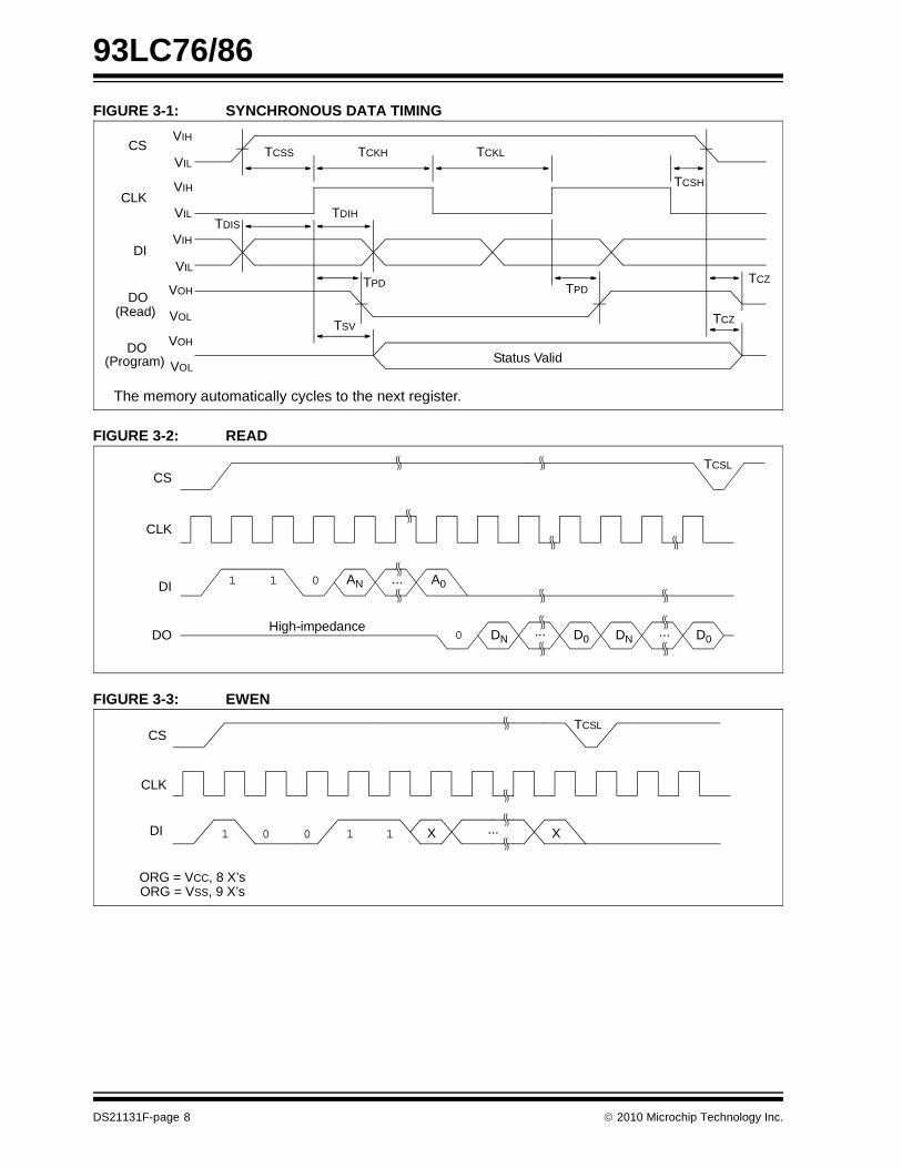
2.3 Erase/Write Enable and Disable (EWEN, EWDS)
The 93LC76/86 powers up in the Erase/Write Disable(EWDS) state. All programming modes must bepreceded by an Erase/Write Enable (EWEN) instruction.Once the EWEN instruction is executed, programmingremains enabled until an EWDS instruction is executedor VCC is removed from the device. To protect againstaccidental data disturb, the EWDS instruction can beused to disable all erase/write functions and shouldfollow all programming operations. Execution of a READinstruction is independent of both the EWEN and EWDSinstructions.
2.4 Data Protection
During power-up, all programming modes of operationare inhibited until VCC has reached a level greater than1.4V. During power-down, the source data protectioncircuitry acts to inhibit all programming modes whenVCC has fallen below 1.4V.
The EWEN and EWDS commands give additionalprotection against accidentally programming duringnormal operation.
After power-up, the device is automatically in theEWDS mode. Therefore, an EWEN instruction must beperformed before any ERASE or WRITE instruction canbe executed.
DS21131F-page 6 2010 Microchip Technology Inc.
93LC76/86
3.0 DEVICE OPERATION
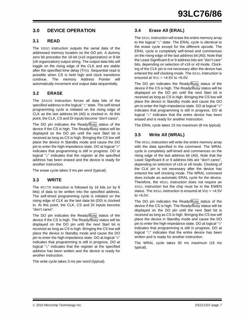
3.1 READ
The READ instruction outputs the serial data of theaddressed memory location on the DO pin. A dummyzero bit precedes the 16-bit (x16 organization) or 8-bit(x8 organization) output string. The output data bits willtoggle on the rising edge of the CLK and are stableafter the specified time delay (TPD). Sequential read ispossible when CS is held high and clock transitionscontinue. The memory Address Pointer willautomatically increment and output data sequentially.
3.2 ERASE
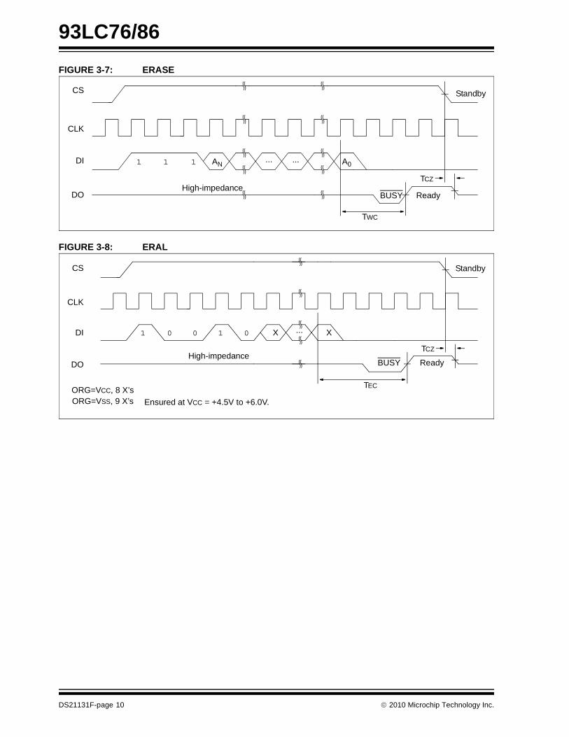
The ERASE instruction forces all data bits of thespecified address to the logical “1” state. The self-timedprogramming cycle is initiated on the rising edge ofCLK as the last address bit (A0) is clocked in. At thispoint, the CLK, CS and DI inputs become “don’t cares”.
The DO pin indicates the Ready/Busy status of thedevice if the CS is high. The Ready/Busy status will bedisplayed on the DO pin until the next Start bit isreceived as long as CS is high. Bringing the CS low willplace the device in Standby mode and cause the DOpin to enter the high-impedance state. DO at logical “0”indicates that programming is still in progress. DO atlogical “1” indicates that the register at the specifiedaddress has been erased and the device is ready foranother instruction.
The erase cycle takes 3 ms per word (typical).
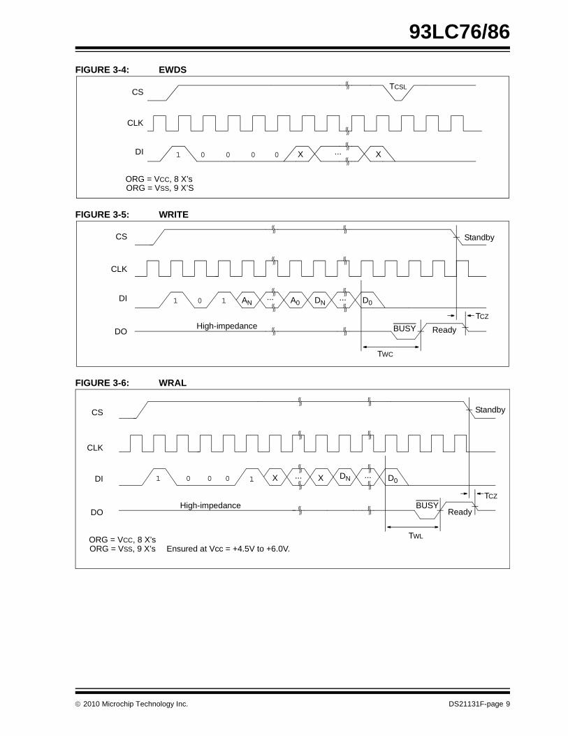
3.3 WRITE
The WRITE instruction is followed by 16 bits (or by 8bits) of data to be written into the specified address.The self-timed programming cycle is initiated on therising edge of CLK as the last data bit (D0) is clockedin. At this point, the CLK, CS and DI inputs become“don’t cares”.
The DO pin indicates the Ready/Busy status of thedevice if the CS is high. The Ready/Busy status will bedisplayed on the DO pin until the next Start bit isreceived as long as CS is high. Bringing the CS low willplace the device in Standby mode and cause the DOpin to enter the high-impedance state. DO at logical “0”indicates that programming is still in progress. DO atlogical “1” indicates that the register at the specifiedaddress has been written and the device is ready foranother instruction.
The write cycle takes 3 ms per word (typical).
3.4 Erase All (ERAL)
The ERAL instruction will erase the entire memory arrayto the logical “1” state. The ERAL cycle is identical tothe erase cycle except for the different opcode. TheERAL cycle is completely self-timed and commenceson the rising edge of the last address bit (A0). Note thatthe Least Significant 8 or 9 address bits are “don’t care”bits, depending on selection of x16 or x8 mode. Clock-ing of the CLK pin is not necessary after the device hasentered the self clocking mode. The ERAL instruction isensured at VCC = +4.5V to +6.0V.
The DO pin indicates the Ready/Busy status of thedevice if the CS is high. The Ready/Busy status will bedisplayed on the DO pin until the next Start bit isreceived as long as CS is high. Bringing the CS low willplace the device in Standby mode and cause the DOpin to enter the high-impedance state. DO at logical “0”indicates that programming is still in progress. DO atlogical “1” indicates that the entire device has beenerased and is ready for another instruction.
The ERAL cycle takes 15 ms maximum (8 ms typical).
3.5 Write All (WRAL)
The WRAL instruction will write the entire memory arraywith the data specified in the command. The WRALcycle is completely self-timed and commences on therising edge of the last address bit (A0). Note that theLeast Significant 8 or 9 address bits are “don’t cares”,depending on selection of x16 or x8 mode. Clocking ofthe CLK pin is not necessary after the device hasentered the self clocking mode. The WRAL commanddoes include an automatic ERAL cycle for the device.Therefore, the WRAL instruction does not require anERAL instruction but the chip must be in the EWENstatus. The WRAL instruction is ensured at Vcc = +4.5Vto +6.0V.
The DO pin indicates the Ready/Busy status of thedevice if the CS is high. The Ready/Busy status will bedisplayed on the DO pin until the next Start bit isreceived as long as CS is high. Bringing the CS low willplace the device in Standby mode and cause the DOpin to enter the high-impedance state. DO at logical “0”indicates that programming is still in progress. DO atlogical “1” indicates that the entire device has beenwritten and is ready for another instruction.
The WRAL cycle takes 30 ms maximum (16 mstypical).
2010 Microchip Technology Inc. DS21131F-page 7
93LC76/86
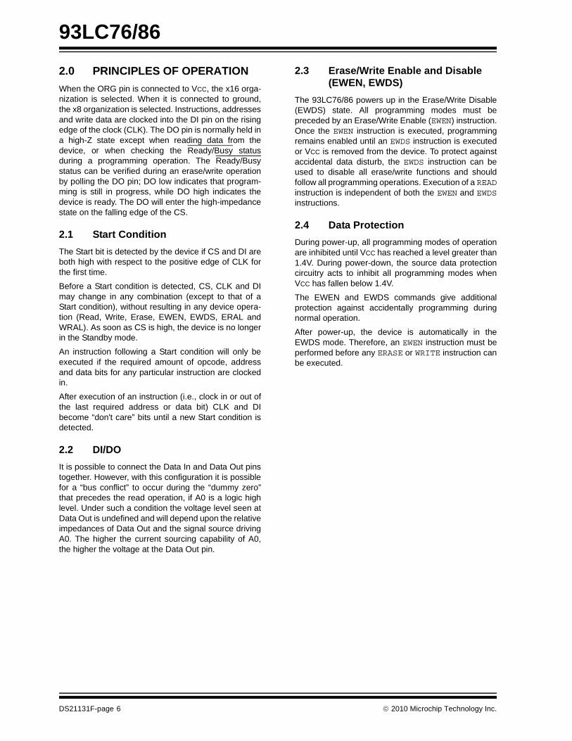
FIGURE 3-1: SYNCHRONOUS DATA TIMING
FIGURE 3-2: READ
FIGURE 3-3: EWEN
The memory automatically cycles to the next register.
VIH
VIL
VIH
VIL
VIH
VOH
VOL
VOH
VOL
VIL
TSV
TDIS
TPD
TDIH
TCSS TCKH TCKL
TPD
TCSH
TCZ
TCZ
CS
CLK
DI
DO
DO(Program)
(Read)
Status Valid
1 1 0 AN A0
DN DND0 D0...
...
...High-impedance
TCSLCS
CLK
DI
DO 0
CS
CLK
DI 1 1 10 0
TCSL
X X...
ORG = VCC, 8 X’sORG = VSS, 9 X’s
DS21131F-page 8 2010 Microchip Technology Inc.
93LC76/86
FIGURE 3-4: EWDS
FIGURE 3-5: WRITE
FIGURE 3-6: WRAL
1 0 0 0 0 X X...
CS
CLK
DI
TCSL
ORG = VCC, 8 X’sORG = VSS, 9 X’S
1 0 1 AN A0... DN
... D0
TWC
ReadyBUSYHigh-impedance
CS
CLK
DI
DO
Standby
TCZ
Ensured at Vcc = +4.5V to +6.0V.
1 0 0 0 1 X ... X DN ... D0
BUSYReady
High-impedance
StandbyCS
CLK
DI
DO
ORG = VCC, 8 X’sORG = VSS, 9 X’s
TWL
TCZ
2010 Microchip Technology Inc. DS21131F-page 9
93LC76/86
FIGURE 3-7: ERASE
FIGURE 3-8: ERAL
1 11 AN... A0
TCZHigh-impedance
CS
CLK
DI
DO
Standby
ReadyBUSY
TWC
...
Ensured at VCC = +4.5V to +6.0V.
ORG=VCC, 8 X’sORG=VSS, 9 X’s
1 00 1 0 X X...
CS
CLK
DI
DO
TEC
TCZHigh-impedance
BUSY Ready
Standby
DS21131F-page 10 2010 Microchip Technology Inc.
93LC76/86
4.0 PIN DESCRIPTIONS
TABLE 4-1: PIN FUNCTION TABLE
4.1 Chip Select (CS)
A high level selects the device. A low level deselectsthe device and forces it into Standby mode. However, aprogramming cycle which is already initiated will becompleted, regardless of the CS input signal. If CS isbrought low during a program cycle, the device will gointo Standby mode as soon as the programming cycleis completed.
CS must be low for 250 ns minimum (TCSL) betweenconsecutive instructions. If CS is low, the internalcontrol logic is held in a Reset status.
4.2 Serial Clock (CLK)
The Serial Clock is used to synchronize the communi-cation between a master device and the 93LC76/86.Opcode, address and data bits are clocked in on thepositive edge of CLK. Data bits are also clocked out onthe positive edge of CLK.
CLK can be stopped anywhere in the transmissionsequence (at high or low level) and can be continuedanytime with respect to clock high time (TCKH) andclock low time (TCKL). This gives the controlling masterfreedom in preparing opcode, address and data.
CLK is a “don't care” if CS is low (device deselected). IfCS is high, but Start condition has not been detected,any number of clock cycles can be received by thedevice without changing its status (i.e., waiting for Startcondition).
CLK cycles are not required during the self-timedWRITE (i.e., auto erase/write) cycle.
After detection of a Start condition the specified numberof clock cycles (respectively low-to-high transitions ofCLK) must be provided. These clock cycles arerequired to clock in all opcode, address, and data bitsbefore an instruction is executed (see Table 1-3through Table 1-6 for more details). CLK and DI thenbecome “don't care” inputs waiting for a new Startcondition to be detected.
4.3 Data In (DI)
Data In is used to clock in a Start bit, opcode, addressand data synchronously with the CLK input.
4.4 Data Out (DO)
Data Out is used in the Read mode to output datasynchronously with the CLK input (TPD after thepositive edge of CLK).
This pin also provides Ready/Busy status informationduring erase and write cycles. Ready/Busy status infor-mation is available when CS is high. It will be displayeduntil the next Start bit occurs as long as CS stays high.
4.5 Organization (ORG)
When ORG is connected to VCC, the x16 memory orga-nization is selected. When ORG is tied to VSS, the x8memory organization is selected. There is an internalpull-up resistor on the ORG pin that will select x16organization when left unconnected.
4.6 Program Enable (PE)
This pin allows the user to enable or disable the abilityto write data to the memory array. If the PE pin isfloated or tied to VCC, the device can be programmed.If the PE pin is tied to VSS, programming will beinhibited. There is an internal pull-up on this device thatenables programming if this pin is left floating.
Name Function
CS Chip Select
CLK Serial Data Clock
DI Serial Data Input
DO Serial Data Output
VSS Ground
ORG Memory Configuration
PE Program Enable
VCC Power Supply
Note: CS must go low between consecutiveinstructions, except when performing asequential read (Refer to Section 3.1“READ” for more detail on sequentialreads).
2010 Microchip Technology Inc. DS21131F-page 11
93LC76/86
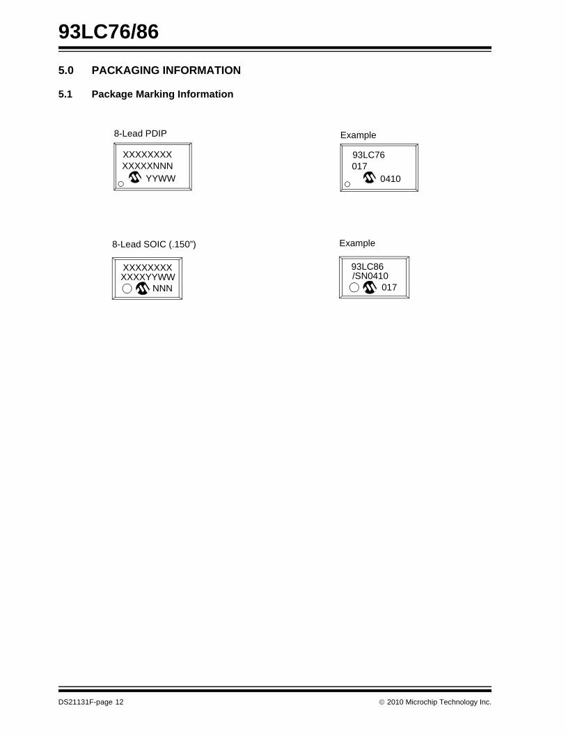
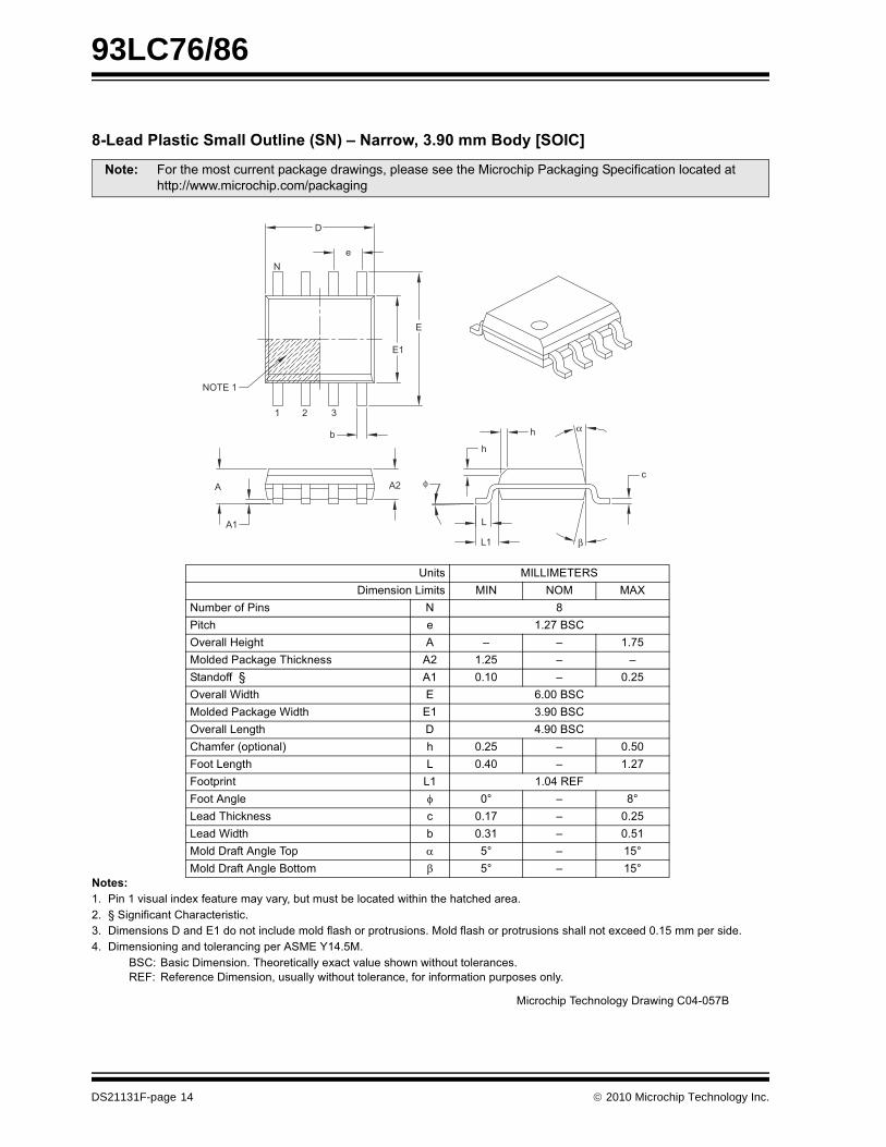
5.0 PACKAGING INFORMATION
5.1 Package Marking Information
XXXXXNNN
8-Lead PDIP
XXXXXXXX
YYWW017
Example
93LC76
0410
8-Lead SOIC (.150”)
XXXXXXXXXXXXYYWW
NNN
Example
93LC86/SN0410
017
DS21131F-page 12 2010 Microchip Technology Inc.
93LC76/86
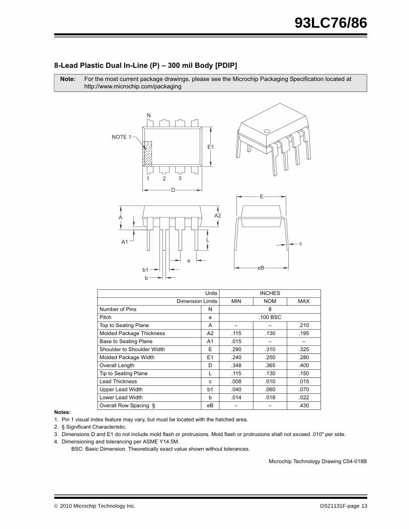
���������� ���������� ������������� ����������
�������� ������ �!"�����#�$�%��&"��'��� ��(�)"&�'"!&�)�����&�#�*�&��&�����&���#������� +������%����&�,����&��!&���-� ��'��!��!�����#�.��#��&�����"#��'�#�%��!����&"!��!����#�%��!����&"!��!�!������&��$���#�����/����!�#���� ��'��!��������#�&���������������.�0������
1�,2�1�!�����'��!���� ���&��������$��&� ��"��!�*��*�&�"&�&������!�
����� 3�&���'!&��"��&����4����#�*���!(�����!��!���&��������������4�����������%���&������&�#��&��&&�255***�'��������'5���4�����
6��&! �7,8.���'��!���9�'�&! ��7 7:� ��;
7"')��%����! 7 <��&�� � �����1�, ��&����&��������� � = = ������#�#����4���� ���4��!! �� ���� ��-� ����1�!��&����&��������� �� ���� = =��"�#��&���"�#��>�#&� . ���� �-�� �-����#�#����4����>�#&� .� ���� ���� ��<�: �����9���&� � �-�< �-?� ���� ���&����&��������� 9 ���� ��-� ����9��#� ���4��!! � ���< ���� ����6����9��#�>�#&� )� ���� ��?� ����9*��9��#�>�#&� ) ���� ���< ����: ������*����������+ �1 = = ��-�
N
E1
NOTE 1
D
1 2 3
A
A1
A2
L
b1b
e
E
eB
c
������� ������� ��*��� ,�����<1
2010 Microchip Technology Inc. DS21131F-page 13
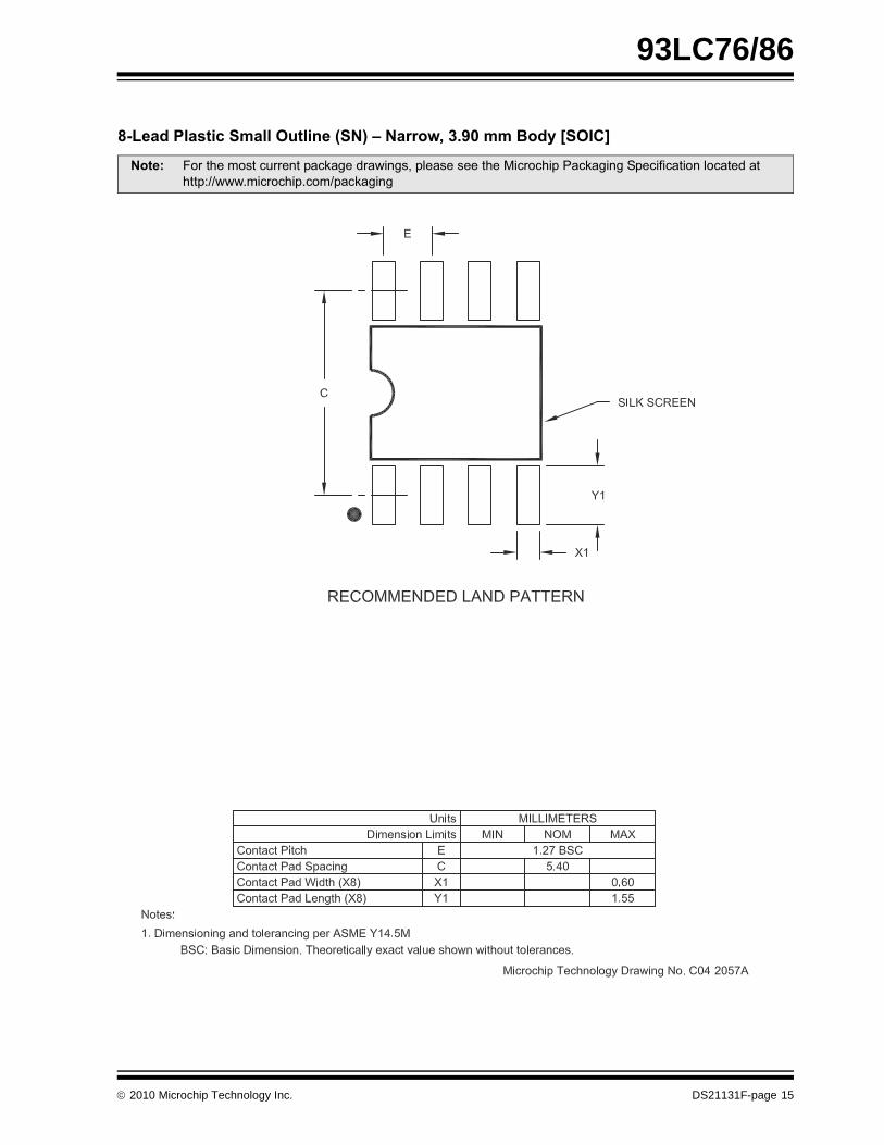
93LC76/86
���������� �� ���!�� ���� �������""�#$��%&����������� !�'�
�������� ������ �!"�����#�$�%��&"��'��� ��(�)"&�'"!&�)�����&�#�*�&����&�����&���#������� +������%����&�,����&��!&���-� ��'��!��!�����#�.��#��&�����"#��'�#�%��!����&"!��!����#�%��!����&"!��!�!������&��$���#������''����!�#���� ��'��!��������#�&���������������.�0������
1�,2 1�!�����'��!���� ���&��������$��&� ��"��!�*��*�&�"&�&������!��.32 ��%��������'��!��(�"!"�����*�&�"&�&������(�%���%'�&����"�!�!�����
����� 3�&���'!&��"��&����4����#�*���!(�����!��!���&��������������4�����������%���&������&�#��&��&&�255***�'��������'5���4�����
6��&! ��99��. .����'��!���9�'�&! ��7 7:� ��;
7"')��%����! 7 <��&�� � �����1�,: �����8����& � = = ������#�#����4���� ���4��!! �� ���� = =�&��#%%��+ �� ���� = ����: �����>�#&� . ?����1�,��#�#����4����>�#&� .� -����1�,: �����9���&� � �����1�,,��'%��@�&����A � ���� = ����3&�9���&� 9 ���� = ����3&���& 9� ������.33&������ � �B = <B9��#� ���4��!! � ���� = ����9��#�>�#&� ) ��-� = ������#���%&������� � � �B = ��B��#���%&�������1&&' � �B = ��B
D
Ne
E
E1
NOTE 1
1 2 3
b
A
A1
A2
L
L1
c
h
h
φ
β
α
������� ������� ��*��� ,������1
DS21131F-page 14 2010 Microchip Technology Inc.
93LC76/86
���������� �� ���!�� ���� �������""�#$��%&����������� !�'�
����� 3�&���'!&��"��&����4����#�*���!(�����!��!���&��������������4�����������%���&������&�#��&��&&�255***�'��������'5���4�����
2010 Microchip Technology Inc. DS21131F-page 15
93LC76/86
APPENDIX A: REVISION HISTORY
Revision E
Added note to page 1 header (Not recommended fornew designs).
Added Section 5.0: Package Marking Information.
Added On-line Support page.
Updated document format.
Revision F
Removed Preliminary Status.
DS21131F-page 16 2010 Microchip Technology Inc.
93LC76/86
ON-LINE SUPPORT
Microchip provides on-line support on the MicrochipWorld Wide Web site.
The web site is used by Microchip as a means to makefiles and information easily available to customers. Toview the site, the user must have access to the Internetand a web browser, such as Netscape® or Microsoft®
Internet Explorer. Files are also available for FTPdownload from our FTP site.
Connecting to the Microchip Internet Web Site
The Microchip web site is available at the followingURL:
www.microchip.com
The file transfer site is available by using an FTPservice to connect to:
ftp://ftp.microchip.com
The web site and file transfer site provide a variety ofservices. Users may download files for the latestDevelopment Tools, Data Sheets, Application Notes,User's Guides, Articles and Sample Programs. A vari-ety of Microchip specific business information is alsoavailable, including listings of Microchip sales offices,distributors and factory representatives. Other dataavailable for consideration is:
• Latest Microchip Press Releases
• Technical Support Section with Frequently Asked Questions
• Design Tips
• Device Errata
• Job Postings
• Microchip Consultant Program Member Listing
• Links to other useful web sites related to Microchip Products
• Conferences for products, Development Systems, technical information and more
• Listing of seminars and events
SYSTEMS INFORMATION AND UPGRADE HOT LINE
The Systems Information and Upgrade Line providessystem users a listing of the latest versions of all ofMicrochip's development systems software products.Plus, this line provides information on how customerscan receive the most current upgrade kits. The Hot LineNumbers are:
1-800-755-2345 for U.S. and most of Canada, and
1-480-792-7302 for the rest of the world.
042003
2010 Microchip Technology Inc. DS21131F-page 17

93LC76/86
READER RESPONSE
It is our intention to provide you with the best documentation possible to ensure successful use of your Microchip prod-uct. If you wish to provide your comments on organization, clarity, subject matter, and ways in which our documentationcan better serve you, please FAX your comments to the Technical Publications Manager at (480) 792-4150.
Please list the following information, and use this outline to provide us with your comments about this document.
To: Technical Publications Manager
RE: Reader Response
Total Pages Sent ________
From: Name
Company
Address
City / State / ZIP / Country
Telephone: (_______) _________ - _________
Application (optional):
Would you like a reply? Y N
Device: Literature Number:
Questions:
FAX: (______) _________ - _________
DS21131F93LC76/86
1. What are the best features of this document?
2. How does this document meet your hardware and software development needs?
3. Do you find the organization of this document easy to follow? If not, why?
4. What additions to the document do you think would enhance the structure and subject?
5. What deletions from the document could be made without affecting the overall usefulness?
6. Is there any incorrect or misleading information (what and where)?
7. How would you improve this document?
DS21131F-page 18 2010 Microchip Technology Inc.
93LC76/86
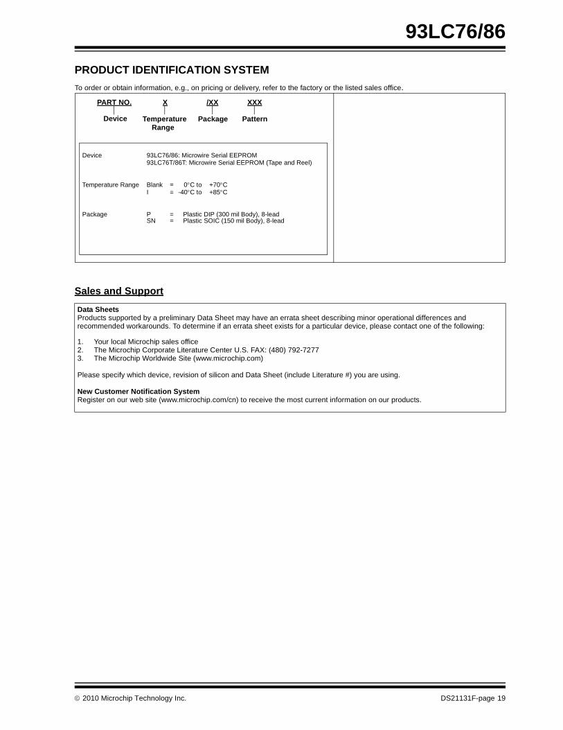
PRODUCT IDENTIFICATION SYSTEM
To order or obtain information, e.g., on pricing or delivery, refer to the factory or the listed sales office.
Sales and Support
PART NO. X /XX XXX
PatternPackageTemperatureRange
Device
Device 93LC76/86: Microwire Serial EEPROM93LC76T/86T: Microwire Serial EEPROM (Tape and Reel)
Temperature Range Blank = 0C to +70CI = -40C to +85C
Package P = Plastic DIP (300 mil Body), 8-leadSN = Plastic SOIC (150 mil Body), 8-lead
Data SheetsProducts supported by a preliminary Data Sheet may have an errata sheet describing minor operational differences and recommended workarounds. To determine if an errata sheet exists for a particular device, please contact one of the following:
1. Your local Microchip sales office2. The Microchip Corporate Literature Center U.S. FAX: (480) 792-72773. The Microchip Worldwide Site (www.microchip.com)
Please specify which device, revision of silicon and Data Sheet (include Literature #) you are using.
New Customer Notification SystemRegister on our web site (www.microchip.com/cn) to receive the most current information on our products.
2010 Microchip Technology Inc. DS21131F-page 19
93LC76/86
NOTES:
DS21131F-page 20 2010 Microchip Technology Inc.
Note the following details of the code protection feature on Microchip devices:
• Microchip products meet the specification contained in their particular Microchip Data Sheet.
• Microchip believes that its family of products is one of the most secure families of its kind on the market today, when used in the intended manner and under normal conditions.
• There are dishonest and possibly illegal methods used to breach the code protection feature. All of these methods, to our knowledge, require using the Microchip products in a manner outside the operating specifications contained in Microchip’s Data Sheets. Most likely, the person doing so is engaged in theft of intellectual property.
• Microchip is willing to work with the customer who is concerned about the integrity of their code.
• Neither Microchip nor any other semiconductor manufacturer can guarantee the security of their code. Code protection does not mean that we are guaranteeing the product as “unbreakable.”
Code protection is constantly evolving. We at Microchip are committed to continuously improving the code protection features of ourproducts. Attempts to break Microchip’s code protection feature may be a violation of the Digital Millennium Copyright Act. If such actsallow unauthorized access to your software or other copyrighted work, you may have a right to sue for relief under that Act.
Information contained in this publication regarding deviceapplications and the like is provided only for your convenienceand may be superseded by updates. It is your responsibility toensure that your application meets with your specifications.MICROCHIP MAKES NO REPRESENTATIONS ORWARRANTIES OF ANY KIND WHETHER EXPRESS ORIMPLIED, WRITTEN OR ORAL, STATUTORY OROTHERWISE, RELATED TO THE INFORMATION,INCLUDING BUT NOT LIMITED TO ITS CONDITION,QUALITY, PERFORMANCE, MERCHANTABILITY ORFITNESS FOR PURPOSE. Microchip disclaims all liabilityarising from this information and its use. Use of Microchipdevices in life support and/or safety applications is entirely atthe buyer’s risk, and the buyer agrees to defend, indemnify andhold harmless Microchip from any and all damages, claims,suits, or expenses resulting from such use. No licenses areconveyed, implicitly or otherwise, under any Microchipintellectual property rights.
2010 Microchip Technology Inc.
Trademarks
The Microchip name and logo, the Microchip logo, dsPIC, KEELOQ, KEELOQ logo, MPLAB, PIC, PICmicro, PICSTART, rfPIC and UNI/O are registered trademarks of Microchip Technology Incorporated in the U.S.A. and other countries.
FilterLab, Hampshire, HI-TECH C, Linear Active Thermistor, MXDEV, MXLAB, SEEVAL and The Embedded Control Solutions Company are registered trademarks of Microchip Technology Incorporated in the U.S.A.
Analog-for-the-Digital Age, Application Maestro, CodeGuard, dsPICDEM, dsPICDEM.net, dsPICworks, dsSPEAK, ECAN, ECONOMONITOR, FanSense, HI-TIDE, In-Circuit Serial Programming, ICSP, Mindi, MiWi, MPASM, MPLAB Certified logo, MPLIB, MPLINK, mTouch, Octopus, Omniscient Code Generation, PICC, PICC-18, PICDEM, PICDEM.net, PICkit, PICtail, PIC32 logo, REAL ICE, rfLAB, Select Mode, Total Endurance, TSHARC, UniWinDriver, WiperLock and ZENA are trademarks of Microchip Technology Incorporated in the U.S.A. and other countries.
SQTP is a service mark of Microchip Technology Incorporated in the U.S.A.
All other trademarks mentioned herein are property of their respective companies.
© 2010, Microchip Technology Incorporated, Printed in the U.S.A., All Rights Reserved.
Printed on recycled paper.
DS21131F-page 21
Microchip received ISO/TS-16949:2002 certification for its worldwide headquarters, design and wafer fabrication facilities in Chandler and Tempe, Arizona; Gresham, Oregon and design centers in California and India. The Company’s quality system processes and procedures are for its PIC® MCUs and dsPIC® DSCs, KEELOQ® code hopping devices, Serial EEPROMs, microperipherals, nonvolatile memory and analog products. In addition, Microchip’s quality system for the design and manufacture of development systems is ISO 9001:2000 certified.
DS21131F-page 22 2010 Microchip Technology Inc.
AMERICASCorporate Office2355 West Chandler Blvd.Chandler, AZ 85224-6199Tel: 480-792-7200 Fax: 480-792-7277Technical Support: http://support.microchip.comWeb Address: www.microchip.com
AtlantaDuluth, GA Tel: 678-957-9614 Fax: 678-957-1455
BostonWestborough, MA Tel: 774-760-0087 Fax: 774-760-0088
ChicagoItasca, IL Tel: 630-285-0071 Fax: 630-285-0075
ClevelandIndependence, OH Tel: 216-447-0464 Fax: 216-447-0643
DallasAddison, TX Tel: 972-818-7423 Fax: 972-818-2924
DetroitFarmington Hills, MI Tel: 248-538-2250Fax: 248-538-2260
KokomoKokomo, IN Tel: 765-864-8360Fax: 765-864-8387
Los AngelesMission Viejo, CA Tel: 949-462-9523 Fax: 949-462-9608
Santa ClaraSanta Clara, CA Tel: 408-961-6444Fax: 408-961-6445
TorontoMississauga, Ontario, CanadaTel: 905-673-0699 Fax: 905-673-6509
ASIA/PACIFICAsia Pacific OfficeSuites 3707-14, 37th FloorTower 6, The GatewayHarbour City, KowloonHong KongTel: 852-2401-1200Fax: 852-2401-3431
Australia - SydneyTel: 61-2-9868-6733Fax: 61-2-9868-6755
China - BeijingTel: 86-10-8528-2100 Fax: 86-10-8528-2104
China - ChengduTel: 86-28-8665-5511Fax: 86-28-8665-7889
China - ChongqingTel: 86-23-8980-9588Fax: 86-23-8980-9500
China - Hong Kong SARTel: 852-2401-1200 Fax: 852-2401-3431
China - NanjingTel: 86-25-8473-2460Fax: 86-25-8473-2470
China - QingdaoTel: 86-532-8502-7355Fax: 86-532-8502-7205
China - ShanghaiTel: 86-21-5407-5533 Fax: 86-21-5407-5066
China - ShenyangTel: 86-24-2334-2829Fax: 86-24-2334-2393
China - ShenzhenTel: 86-755-8203-2660 Fax: 86-755-8203-1760
China - WuhanTel: 86-27-5980-5300Fax: 86-27-5980-5118
China - XianTel: 86-29-8833-7252Fax: 86-29-8833-7256
China - XiamenTel: 86-592-2388138 Fax: 86-592-2388130
China - ZhuhaiTel: 86-756-3210040 Fax: 86-756-3210049
ASIA/PACIFICIndia - BangaloreTel: 91-80-3090-4444 Fax: 91-80-3090-4123
India - New DelhiTel: 91-11-4160-8631Fax: 91-11-4160-8632
India - PuneTel: 91-20-2566-1512Fax: 91-20-2566-1513
Japan - YokohamaTel: 81-45-471- 6166 Fax: 81-45-471-6122
Korea - DaeguTel: 82-53-744-4301Fax: 82-53-744-4302
Korea - SeoulTel: 82-2-554-7200Fax: 82-2-558-5932 or 82-2-558-5934
Malaysia - Kuala LumpurTel: 60-3-6201-9857Fax: 60-3-6201-9859
Malaysia - PenangTel: 60-4-227-8870Fax: 60-4-227-4068
Philippines - ManilaTel: 63-2-634-9065Fax: 63-2-634-9069
SingaporeTel: 65-6334-8870Fax: 65-6334-8850
Taiwan - Hsin ChuTel: 886-3-6578-300Fax: 886-3-6578-370
Taiwan - KaohsiungTel: 886-7-536-4818Fax: 886-7-536-4803
Taiwan - TaipeiTel: 886-2-2500-6610 Fax: 886-2-2508-0102
Thailand - BangkokTel: 66-2-694-1351Fax: 66-2-694-1350
EUROPEAustria - WelsTel: 43-7242-2244-39Fax: 43-7242-2244-393Denmark - CopenhagenTel: 45-4450-2828 Fax: 45-4485-2829
France - ParisTel: 33-1-69-53-63-20 Fax: 33-1-69-30-90-79
Germany - MunichTel: 49-89-627-144-0 Fax: 49-89-627-144-44
Italy - Milan Tel: 39-0331-742611 Fax: 39-0331-466781
Netherlands - DrunenTel: 31-416-690399 Fax: 31-416-690340
Spain - MadridTel: 34-91-708-08-90Fax: 34-91-708-08-91
UK - WokinghamTel: 44-118-921-5869Fax: 44-118-921-5820
WORLDWIDE SALES AND SERVICE
01/05/10