Embed Size (px)
Citation preview

1/34April 2004
M93S66, M93S56M93S46
4Kbit, 2Kbit and 1Kbit (16-bit wide)MICROWIRE Serial Access EEPROM with Block Protection
FEATURES SUMMARY Industry Standard MICROWIRE Bus Single Supply Voltage:
– 4.5 to 5.5V for M93Sx6– 2.5 to 5.5V for M93Sx6-W– 1.8 to 5.5V for M93Sx6-R
Single Organization: by Word (x16) Programming Instructions that work on: Word
or Entire Memory Self-timed Programming Cycle with Auto-
Erase User Defined Write Protected Area Page Write Mode (4 words) Ready/Busy Signal During Programming Speed:
– 1MHz Clock Rate, 10ms Write Time (Current product, identified by process identification letter F or M)
– 2MHz Clock Rate, 5ms Write Time (New Product, identified by process identification letter W or G)
Sequential Read Operation Enhanced ESD/Latch-Up Behavior More than 1 Million Erase/Write Cycles More than 40 Year Data Retention
Figure 1. Packages
PDIP8 (BN)
8
1
SO8 (MN)150 mil width
8
1
TSSOP8 (DW)169 mil width
TSSOP8 (DS)3x3mm body size
M93S66, M93S56, M93S46
2/34
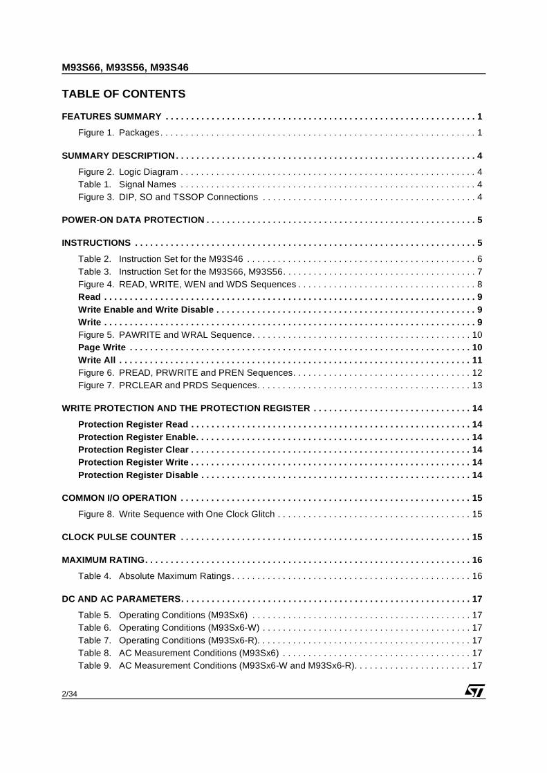
TABLE OF CONTENTS
FEATURES SUMMARY . . . . . . . . . . . . . . . . . . . . . . . . . . . . . . . . . . . . . . . . . . . . . . . . . . . . . . . . . . . . . 1
Figure 1. Packages. . . . . . . . . . . . . . . . . . . . . . . . . . . . . . . . . . . . . . . . . . . . . . . . . . . . . . . . . . . . . . 1
SUMMARY DESCRIPTION. . . . . . . . . . . . . . . . . . . . . . . . . . . . . . . . . . . . . . . . . . . . . . . . . . . . . . . . . . . 4
Figure 2. Logic Diagram . . . . . . . . . . . . . . . . . . . . . . . . . . . . . . . . . . . . . . . . . . . . . . . . . . . . . . . . . . 4Table 1. Signal Names . . . . . . . . . . . . . . . . . . . . . . . . . . . . . . . . . . . . . . . . . . . . . . . . . . . . . . . . . . 4Figure 3. DIP, SO and TSSOP Connections . . . . . . . . . . . . . . . . . . . . . . . . . . . . . . . . . . . . . . . . . . 4
POWER-ON DATA PROTECTION . . . . . . . . . . . . . . . . . . . . . . . . . . . . . . . . . . . . . . . . . . . . . . . . . . . . . 5
INSTRUCTIONS . . . . . . . . . . . . . . . . . . . . . . . . . . . . . . . . . . . . . . . . . . . . . . . . . . . . . . . . . . . . . . . . . . . 5
Table 2. Instruction Set for the M93S46 . . . . . . . . . . . . . . . . . . . . . . . . . . . . . . . . . . . . . . . . . . . . . 6Table 3. Instruction Set for the M93S66, M93S56. . . . . . . . . . . . . . . . . . . . . . . . . . . . . . . . . . . . . . 7Figure 4. READ, WRITE, WEN and WDS Sequences . . . . . . . . . . . . . . . . . . . . . . . . . . . . . . . . . . . 8Read . . . . . . . . . . . . . . . . . . . . . . . . . . . . . . . . . . . . . . . . . . . . . . . . . . . . . . . . . . . . . . . . . . . . . . . . . 9Write Enable and Write Disable . . . . . . . . . . . . . . . . . . . . . . . . . . . . . . . . . . . . . . . . . . . . . . . . . . . 9Write . . . . . . . . . . . . . . . . . . . . . . . . . . . . . . . . . . . . . . . . . . . . . . . . . . . . . . . . . . . . . . . . . . . . . . . . . 9Figure 5. PAWRITE and WRAL Sequence. . . . . . . . . . . . . . . . . . . . . . . . . . . . . . . . . . . . . . . . . . . 10Page Write . . . . . . . . . . . . . . . . . . . . . . . . . . . . . . . . . . . . . . . . . . . . . . . . . . . . . . . . . . . . . . . . . . . 10Write All . . . . . . . . . . . . . . . . . . . . . . . . . . . . . . . . . . . . . . . . . . . . . . . . . . . . . . . . . . . . . . . . . . . . . 11Figure 6. PREAD, PRWRITE and PREN Sequences. . . . . . . . . . . . . . . . . . . . . . . . . . . . . . . . . . . 12Figure 7. PRCLEAR and PRDS Sequences. . . . . . . . . . . . . . . . . . . . . . . . . . . . . . . . . . . . . . . . . . 13
WRITE PROTECTION AND THE PROTECTION REGISTER . . . . . . . . . . . . . . . . . . . . . . . . . . . . . . . 14
Protection Register Read . . . . . . . . . . . . . . . . . . . . . . . . . . . . . . . . . . . . . . . . . . . . . . . . . . . . . . . 14Protection Register Enable. . . . . . . . . . . . . . . . . . . . . . . . . . . . . . . . . . . . . . . . . . . . . . . . . . . . . . 14Protection Register Clear . . . . . . . . . . . . . . . . . . . . . . . . . . . . . . . . . . . . . . . . . . . . . . . . . . . . . . . 14Protection Register Write . . . . . . . . . . . . . . . . . . . . . . . . . . . . . . . . . . . . . . . . . . . . . . . . . . . . . . . 14Protection Register Disable . . . . . . . . . . . . . . . . . . . . . . . . . . . . . . . . . . . . . . . . . . . . . . . . . . . . . 14
COMMON I/O OPERATION . . . . . . . . . . . . . . . . . . . . . . . . . . . . . . . . . . . . . . . . . . . . . . . . . . . . . . . . . 15
Figure 8. Write Sequence with One Clock Glitch . . . . . . . . . . . . . . . . . . . . . . . . . . . . . . . . . . . . . . 15
CLOCK PULSE COUNTER . . . . . . . . . . . . . . . . . . . . . . . . . . . . . . . . . . . . . . . . . . . . . . . . . . . . . . . . . 15
MAXIMUM RATING. . . . . . . . . . . . . . . . . . . . . . . . . . . . . . . . . . . . . . . . . . . . . . . . . . . . . . . . . . . . . . . . 16
Table 4. Absolute Maximum Ratings. . . . . . . . . . . . . . . . . . . . . . . . . . . . . . . . . . . . . . . . . . . . . . . 16
DC AND AC PARAMETERS. . . . . . . . . . . . . . . . . . . . . . . . . . . . . . . . . . . . . . . . . . . . . . . . . . . . . . . . . 17
Table 5. Operating Conditions (M93Sx6) . . . . . . . . . . . . . . . . . . . . . . . . . . . . . . . . . . . . . . . . . . . 17Table 6. Operating Conditions (M93Sx6-W) . . . . . . . . . . . . . . . . . . . . . . . . . . . . . . . . . . . . . . . . . 17Table 7. Operating Conditions (M93Sx6-R). . . . . . . . . . . . . . . . . . . . . . . . . . . . . . . . . . . . . . . . . . 17Table 8. AC Measurement Conditions (M93Sx6) . . . . . . . . . . . . . . . . . . . . . . . . . . . . . . . . . . . . . 17Table 9. AC Measurement Conditions (M93Sx6-W and M93Sx6-R). . . . . . . . . . . . . . . . . . . . . . . 17

3/34
M93S66, M93S56, M93S46
Figure 9. AC Testing Input Output Waveforms . . . . . . . . . . . . . . . . . . . . . . . . . . . . . . . . . . . . . . . . 18Table 10. Capacitance. . . . . . . . . . . . . . . . . . . . . . . . . . . . . . . . . . . . . . . . . . . . . . . . . . . . . . . . . . . 18Table 11. DC Characteristics (M93Sx6, Device Grade 6) . . . . . . . . . . . . . . . . . . . . . . . . . . . . . . . . 19Table 12. DC Characteristics (M93Sx6, Device Grade 3) . . . . . . . . . . . . . . . . . . . . . . . . . . . . . . . . 19Table 13. DC Characteristics (M93Sx6-W, Device Grade 6). . . . . . . . . . . . . . . . . . . . . . . . . . . . . . 20Table 14. DC Characteristics (M93Sx6-W, Device Grade 3). . . . . . . . . . . . . . . . . . . . . . . . . . . . . . 21Table 15. DC Characteristics (M93Sx6-R) . . . . . . . . . . . . . . . . . . . . . . . . . . . . . . . . . . . . . . . . . . . 21Table 16. AC Characteristics (M93Sx6, Device Grade 6 or 3) . . . . . . . . . . . . . . . . . . . . . . . . . . . . 22Table 17. AC Characteristics (M93Sx6-W, Device Grade 6). . . . . . . . . . . . . . . . . . . . . . . . . . . . . . 23Table 18. AC Characteristics (M93Sx6-W, Device Grade 3). . . . . . . . . . . . . . . . . . . . . . . . . . . . . . 24Table 19. AC Characteristics (M93Sx6-R). . . . . . . . . . . . . . . . . . . . . . . . . . . . . . . . . . . . . . . . . . . . 25Figure 10.Synchronous Timing (Start and Op-Code Input) . . . . . . . . . . . . . . . . . . . . . . . . . . . . . . . 26Figure 11.Synchronous Timing (Read or Write) . . . . . . . . . . . . . . . . . . . . . . . . . . . . . . . . . . . . . . . 26Figure 12.Synchronous Timing (Read or Write) . . . . . . . . . . . . . . . . . . . . . . . . . . . . . . . . . . . . . . . 27
PACKAGE MECHANICAL . . . . . . . . . . . . . . . . . . . . . . . . . . . . . . . . . . . . . . . . . . . . . . . . . . . . . . . . . . 28
Figure 13.PDIP8 – 8 pin Plastic DIP, 0.25mm lead frame, Package Outline . . . . . . . . . . . . . . . . . 28Table 20. PDIP8 – 8 pin Plastic DIP, 0.25mm lead frame, Package Mechanical Data . . . . . . . . . . 28Figure 14.SO8 narrow – 8 lead Plastic Small Outline, 150 mils body width, Package Outline . . . . 29Table 21. SO8 narrow – 8 lead Plastic Small Outline, 150 mils body width, Package Mechanical Data29Figure 15.TSSOP8 3x3mm² – 8 lead Thin Shrink Small Outline, 3x3mm² body size, Package Outline30Table 22. TSSOP8 3x3mm² – 8 lead Thin Shrink Small Outline, 3x3mm² body size, Mechanical Data30Figure 16.TSSOP8 – 8 lead Thin Shrink Small Outline, Package Outline . . . . . . . . . . . . . . . . . . . 31Table 23. TSSOP8 – 8 lead Thin Shrink Small Outline, Package Mechanical Data . . . . . . . . . . . . 31
PART NUMBERING . . . . . . . . . . . . . . . . . . . . . . . . . . . . . . . . . . . . . . . . . . . . . . . . . . . . . . . . . . . . . . . 32
Table 24. Ordering Information Scheme . . . . . . . . . . . . . . . . . . . . . . . . . . . . . . . . . . . . . . . . . . . . . 32Table 25. How to Identify Current and New Products by the Process Identification Letter . . . . . . . 32
REVISION HISTORY. . . . . . . . . . . . . . . . . . . . . . . . . . . . . . . . . . . . . . . . . . . . . . . . . . . . . . . . . . . . . . . 33
Table 26. Document Revision History . . . . . . . . . . . . . . . . . . . . . . . . . . . . . . . . . . . . . . . . . . . . . . . 33
M93S66, M93S56, M93S46
4/34
SUMMARY DESCRIPTIONThis specification covers a range of 4K, 2K, 1K bitserial Electrically Erasable Programmable Memo-ry (EEPROM) products (respectively for M93S66,M93S56, M93S46). In this text, these products arecollectively referred to as M93Sx6.
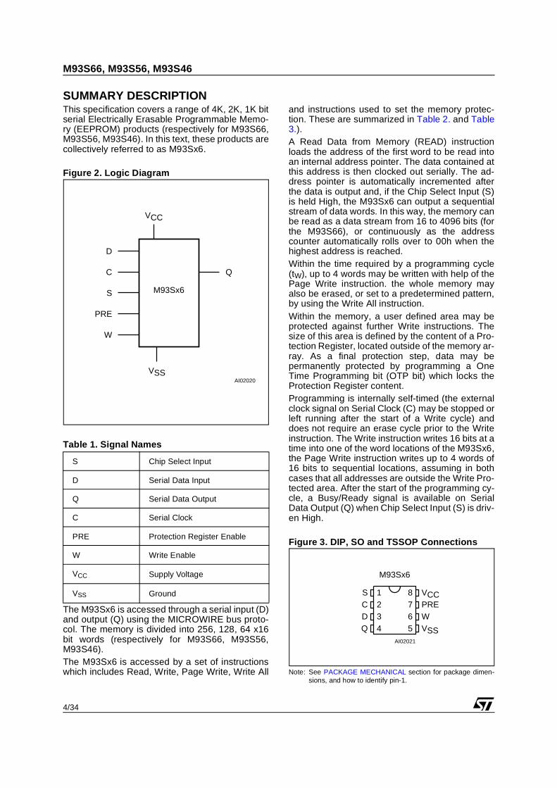
Figure 2. Logic Diagram
Table 1. Signal Names
The M93Sx6 is accessed through a serial input (D)and output (Q) using the MICROWIRE bus proto-col. The memory is divided into 256, 128, 64 x16bit words (respectively for M93S66, M93S56,M93S46).The M93Sx6 is accessed by a set of instructionswhich includes Read, Write, Page Write, Write All
and instructions used to set the memory protec-tion. These are summarized in Table 2. and Table3.).A Read Data from Memory (READ) instructionloads the address of the first word to be read intoan internal address pointer. The data contained atthis address is then clocked out serially. The ad-dress pointer is automatically incremented afterthe data is output and, if the Chip Select Input (S)is held High, the M93Sx6 can output a sequentialstream of data words. In this way, the memory canbe read as a data stream from 16 to 4096 bits (forthe M93S66), or continuously as the addresscounter automatically rolls over to 00h when thehighest address is reached.Within the time required by a programming cycle(tW), up to 4 words may be written with help of thePage Write instruction. the whole memory mayalso be erased, or set to a predetermined pattern,by using the Write All instruction. Within the memory, a user defined area may beprotected against further Write instructions. Thesize of this area is defined by the content of a Pro-tection Register, located outside of the memory ar-ray. As a final protection step, data may bepermanently protected by programming a OneTime Programming bit (OTP bit) which locks theProtection Register content.Programming is internally self-timed (the externalclock signal on Serial Clock (C) may be stopped orleft running after the start of a Write cycle) anddoes not require an erase cycle prior to the Writeinstruction. The Write instruction writes 16 bits at atime into one of the word locations of the M93Sx6,the Page Write instruction writes up to 4 words of16 bits to sequential locations, assuming in bothcases that all addresses are outside the Write Pro-tected area. After the start of the programming cy-cle, a Busy/Ready signal is available on SerialData Output (Q) when Chip Select Input (S) is driv-en High.
Figure 3. DIP, SO and TSSOP Connections
Note: See PACKAGE MECHANICAL section for package dimen-sions, and how to identify pin-1.
S Chip Select Input
D Serial Data Input
Q Serial Data Output
C Serial Clock
PRE Protection Register Enable
W Write Enable
VCC Supply Voltage
VSS Ground
AI02020
D
VCC
M93Sx6
VSS
C Q
PRE
W
S
VSSQWPREC
S VCC
D
AI02021
M93Sx6
1234
8765

5/34
M93S66, M93S56, M93S46
An internal Power-on Data Protection mechanismin the M93Sx6 inhibits the device when the supplyis too low.
POWER-ON DATA PROTECTIONTo prevent data corruption and inadvertent writeoperations during power-up, a Power-On Reset(POR) circuit resets all internal programming cir-cuitry, and sets the device in the Write Disablemode. – At Power-up and Power-down, the device
must not be selected (that is, Chip Select Input (S) must be driven Low) until the supply voltage reaches the operating value VCC specified in Table 5. to Table 6..
– When VCC reaches its valid level, the device is properly reset (in the Write Disable mode) and is ready to decode and execute incoming instructions.
For the M93Sx6 devices (5V range) the PORthreshold voltage is around 3V. For the M93Sx6-W (3V range) and M93Sx6-R (2V range) the PORthreshold voltage is around 1.5V.
INSTRUCTIONSThe instruction set of the M93Sx6 devices con-tains seven instructions, as summarized in Table2. to Table 3.. Each instruction consists of the fol-lowing parts, as shown in Figure 4.: Each instruction is preceded by a rising edge
on Chip Select Input (S) with Serial Clock (C) being held Low.
A start bit, which is the first ‘1’ read on Serial Data Input (D) during the rising edge of Serial Clock (C).
Two op-code bits, read on Serial Data Input (D) during the rising edge of Serial Clock (C). (Some instructions also use the first two bits of the address to define the op-code).
The address bits of the byte or word that is to be accessed. For the M93S46, the address is made up of 6 bits (see Table 2.). For the M93S56 and M93S66, the address is made up of 8 bits (see Table 3.).
The M93Sx6 devices are fabricated in CMOStechnology and are therefore able to run as slowas 0 Hz (static input signals) or as fast as the max-imum ratings specified in Table 16. to Table 19..

M93S66, M93S56, M93S46
6/34
Table 2. Instruction Set for the M93S46
Note: 1. X = Don’t Care bit.
Instruction Description W PRE Start bit
Op-Code Address1 Data
Required Clock Cycles
Additional Comments
READ Read Data from Memory
X 0 1 10 A5-A0 Q15-Q0
WRITEWrite Data to Memory
1 0 1 01 A5-A0 D15-D0 25
Write is executed if the address is not inside the Protected area
PAWRITE Page Write to Memory
1 0 1 11 A5-A0 N x D15-D0
9 + N x 16
Write is executed if all the N addresses are not inside the Protected area
WRAL
Write All Memory with same Data
1 0 1 00 01 XXXX D15-D0 25Write all data if the Protection Register is cleared
WEN Write Enable 1 0 1 00 11 XXXX 9
WDS Write Disable X 0 1 00 00 XXXX 9
PRREADProtection Register Read
X 1 1 10 XXXXXXQ5-Q0+ Flag
Data Output = Protection Register content + Protection Flag bit
PRWRITEProtection Register Write
1 1 1 01 A5-A0 9Data above specified address A5-A0 are protected
PRCLEARProtection Register Clear
1 1 1 11 111111 9Protect Flag is also cleared (cleared Flag = 1)
PRENProtection Register Enable
1 1 1 00 11XXXX 9
PRDSProtection Register Disable
1 1 1 00 000000 9OTP bit is set permanently
7/34
M93S66, M93S56, M93S46
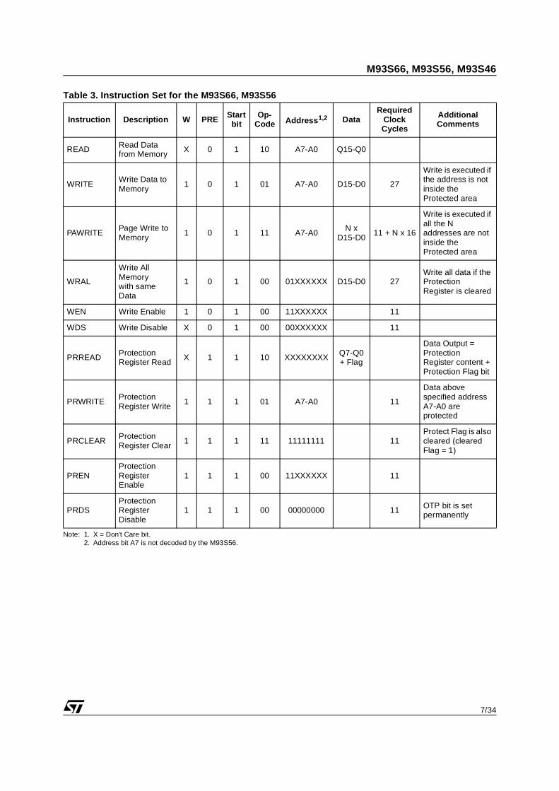
Table 3. Instruction Set for the M93S66, M93S56
Note: 1. X = Don’t Care bit.2. Address bit A7 is not decoded by the M93S56.
Instruction Description W PRE Start bit
Op-Code Address1,2 Data
Required Clock Cycles
Additional Comments
READ Read Data from Memory
X 0 1 10 A7-A0 Q15-Q0
WRITEWrite Data to Memory
1 0 1 01 A7-A0 D15-D0 27
Write is executed if the address is not inside the Protected area
PAWRITEPage Write to Memory
1 0 1 11 A7-A0N x
D15-D011 + N x 16
Write is executed if all the N addresses are not inside the Protected area
WRAL
Write All Memory with same Data
1 0 1 00 01XXXXXX D15-D0 27Write all data if the Protection Register is cleared
WEN Write Enable 1 0 1 00 11XXXXXX 11
WDS Write Disable X 0 1 00 00XXXXXX 11
PRREAD Protection Register Read
X 1 1 10 XXXXXXXX Q7-Q0+ Flag
Data Output = Protection Register content + Protection Flag bit
PRWRITEProtection Register Write
1 1 1 01 A7-A0 11
Data above specified address A7-A0 are protected
PRCLEARProtection Register Clear
1 1 1 11 11111111 11Protect Flag is also cleared (cleared Flag = 1)
PRENProtection Register Enable
1 1 1 00 11XXXXXX 11
PRDSProtection Register Disable
1 1 1 00 00000000 11 OTP bit is set permanently

M93S66, M93S56, M93S46
8/34
Figure 4. READ, WRITE, WEN and WDS Sequences
Note: For the meanings of An, Xn, Qn and Dn, see Table 2. and Table 3..
AI00889D
1 1 0 An A0
Qn Q0
DATA OUT
D
S
Q
S
WRITE
ADDROP
CODE
1 0 An A0
DATA IN
D
Q
OPCODE
Dn D01
BUSY READY
S
WRITEENABLE
1 0 Xn X0D
OPCODE
10 1
S
WRITEDISABLE
1 0 Xn X0D
OPCODE
0 00
CHECKSTATUS
ADDR
PREREAD
PRE
W
PRE
W
PRE
9/34
M93S66, M93S56, M93S46
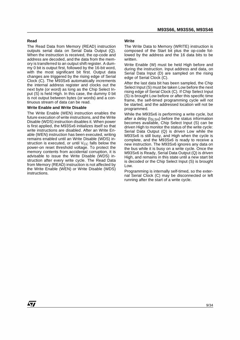
ReadThe Read Data from Memory (READ) instructionoutputs serial data on Serial Data Output (Q).When the instruction is received, the op-code andaddress are decoded, and the data from the mem-ory is transferred to an output shift register. A dum-my 0 bit is output first, followed by the 16-bit word,with the most significant bit first. Output datachanges are triggered by the rising edge of SerialClock (C). The M93Sx6 automatically incrementsthe internal address register and clocks out thenext byte (or word) as long as the Chip Select In-put (S) is held High. In this case, the dummy 0 bitis not output between bytes (or words) and a con-tinuous stream of data can be read.Write Enable and Write DisableThe Write Enable (WEN) instruction enables thefuture execution of write instructions, and the WriteDisable (WDS) instruction disables it. When poweris first applied, the M93Sx6 initializes itself so thatwrite instructions are disabled. After an Write En-able (WEN) instruction has been executed, writingremains enabled until an Write Disable (WDS) in-struction is executed, or until VCC falls below thepower-on reset threshold voltage. To protect thememory contents from accidental corruption, it isadvisable to issue the Write Disable (WDS) in-struction after every write cycle. The Read Datafrom Memory (READ) instruction is not affected bythe Write Enable (WEN) or Write Disable (WDS)instructions.
WriteThe Write Data to Memory (WRITE) instruction iscomposed of the Start bit plus the op-code fol-lowed by the address and the 16 data bits to bewritten.Write Enable (W) must be held High before andduring the instruction. Input address and data, onSerial Data Input (D) are sampled on the risingedge of Serial Clock (C).After the last data bit has been sampled, the ChipSelect Input (S) must be taken Low before the nextrising edge of Serial Clock (C). If Chip Select Input(S) is brought Low before or after this specific timeframe, the self-timed programming cycle will notbe started, and the addressed location will not beprogrammed.While the M93Sx6 is performing a write cycle, butafter a delay (tSLSH) before the status informationbecomes available, Chip Select Input (S) can bedriven High to monitor the status of the write cycle:Serial Data Output (Q) is driven Low while theM93Sx6 is still busy, and High when the cycle iscomplete, and the M93Sx6 is ready to receive anew instruction. The M93Sx6 ignores any data onthe bus while it is busy on a write cycle. Once theM93Sx6 is Ready, Serial Data Output (Q) is drivenHigh, and remains in this state until a new start bitis decoded or the Chip Select Input (S) is broughtLow.Programming is internally self-timed, so the exter-nal Serial Clock (C) may be disconnected or leftrunning after the start of a write cycle.
M93S66, M93S56, M93S46
10/34
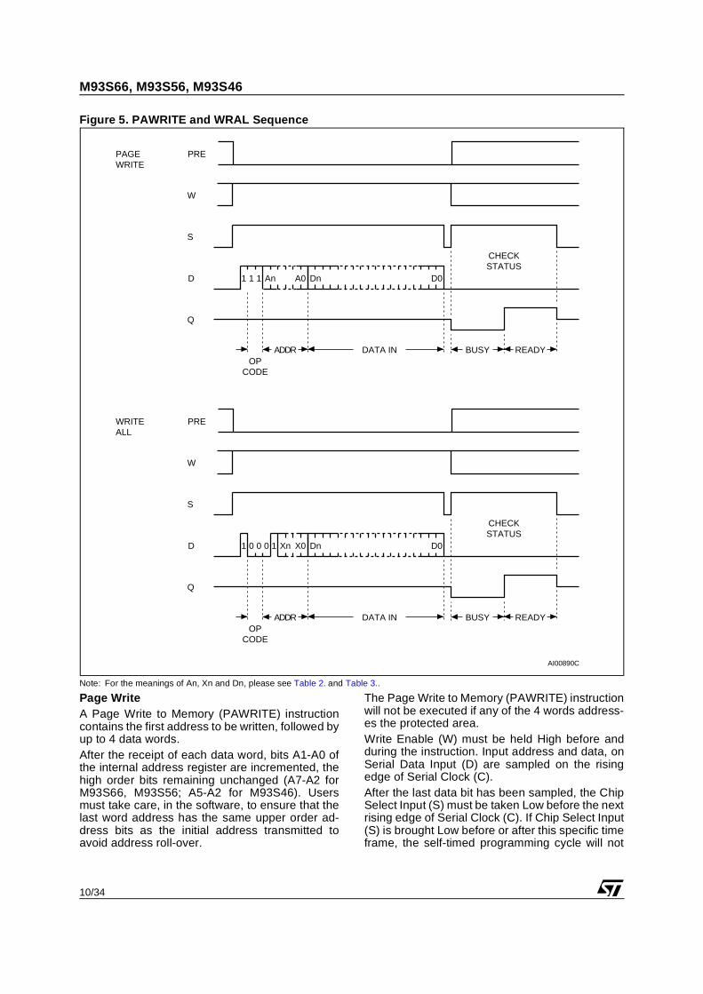
Figure 5. PAWRITE and WRAL Sequence
Note: For the meanings of An, Xn and Dn, please see Table 2. and Table 3..
Page WriteA Page Write to Memory (PAWRITE) instructioncontains the first address to be written, followed byup to 4 data words.After the receipt of each data word, bits A1-A0 ofthe internal address register are incremented, thehigh order bits remaining unchanged (A7-A2 forM93S66, M93S56; A5-A2 for M93S46). Usersmust take care, in the software, to ensure that thelast word address has the same upper order ad-dress bits as the initial address transmitted toavoid address roll-over.
The Page Write to Memory (PAWRITE) instructionwill not be executed if any of the 4 words address-es the protected area.Write Enable (W) must be held High before andduring the instruction. Input address and data, onSerial Data Input (D) are sampled on the risingedge of Serial Clock (C).After the last data bit has been sampled, the ChipSelect Input (S) must be taken Low before the nextrising edge of Serial Clock (C). If Chip Select Input(S) is brought Low before or after this specific timeframe, the self-timed programming cycle will not
AI00890C
S
PAGEWRITE
1 1 An A0
DATA IN
D
Q
OPCODE
Dn D01
BUSY READY
CHECKSTATUS
ADDR
PRE
W
S
WRITEALL
1 0 Xn X0
DATA IN
D
Q
OPCODE
Dn D00
BUSY READY
CHECKSTATUS
ADDR
PRE
W
0 1
11/34
M93S66, M93S56, M93S46
be started, and the addressed location will not beprogrammed.While the M93Sx6 is performing a write cycle, butafter a delay (tSLSH) before the status informationbecomes available, Chip Select Input (S) can bedriven High to monitor the status of the write cycle:Serial Data Output (Q) is driven Low while theM93Sx6 is still busy, and High when the cycle iscomplete, and the M93Sx6 is ready to receive anew instruction. The M93Sx6 ignores any data onthe bus while it is busy on a write cycle. Once theM93Sx6 is Ready, Serial Data Output (Q) is drivenHigh, and remains in this state until a new start bitis decoded or the Chip Select Input (S) is broughtLow.Programming is internally self-timed, so the exter-nal Serial Clock (C) may be disconnected or leftrunning after the start of a write cycle.Write AllThe Write All Memory with same Data (WRAL) in-struction is valid only after the Protection Registerhas been cleared by executing a Protection Reg-ister Clear (PRCLEAR) instruction. The Write AllMemory with same Data (WRAL) instruction simul-taneously writes the whole memory with the samedata word given in the instruction.
Write Enable (W) must be held High before andduring the instruction. Input address and data, onSerial Data Input (D) are sampled on the risingedge of Serial Clock (C).After the last data bit has been sampled, the ChipSelect Input (S) must be taken Low before the nextrising edge of Serial Clock (C). If Chip Select Input(S) is brought Low before or after this specific timeframe, the self-timed programming cycle will notbe started, and the addressed location will not beprogrammed.While the M93Sx6 is performing a write cycle, butafter a delay (tSLSH) before the status informationbecomes available, Chip Select Input (S) can bedriven High to monitor the status of the write cycle:Serial Data Output (Q) is driven Low while theM93Sx6 is still busy, and High when the cycle iscomplete, and the M93Sx6 is ready to receive anew instruction. The M93Sx6 ignores any data onthe bus while it is busy on a write cycle. Once theM93Sx6 is Ready, Serial Data Output (Q) is drivenHigh, and remains in this state until a new start bitis decoded or the Chip Select Input (S) is broughtLow.Programming is internally self-timed, so the exter-nal Serial Clock (C) may be disconnected or leftrunning after the start of a write cycle.
M93S66, M93S56, M93S46
12/34
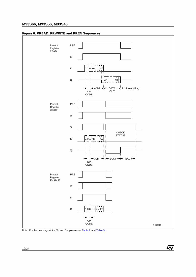
Figure 6. PREAD, PRWRITE and PREN Sequences
Note: For the meanings of An, Xn and Dn, please see Table 2. and Table 3..
AI00891D
1 1 0 Xn X0
DATAOUT
D
S
Q
S
ProtectRegisterWRITE
ADDROP
CODE
1 0 An A0D
Q
OPCODE
1
BUSY READY
S
ProtectRegisterENABLE
1 0 Xn X0D
OPCODE
10 1
CHECKSTATUS
ADDR
PREProtectRegisterREAD
PRE
W
PRE
W
An A0 F
F = Protect Flag

13/34
M93S66, M93S56, M93S46
Figure 7. PRCLEAR and PRDS Sequences
Note: For the meanings of An, Xn and Dn, please see Table 2. and Table 3..
AI00892C
S
ProtectRegisterCLEAR
1 1D
Q
OPCODE
1
BUSY READY
CHECKSTATUS
ADDR
PRE
W
1 1 1
S
ProtectRegisterDISABLE
1 0D
Q
OPCODE
0
BUSY READY
CHECKSTATUS
ADDR
PRE
W
0 0 0
M93S66, M93S56, M93S46
14/34
WRITE PROTECTION AND THE PROTECTION REGISTERThe Protection Register on the M93Sx6 is used toadjust the amount of memory that is to be writeprotected. The write protected area extends fromthe address given in the Protection Register, up tothe top address in the M93Sx6 device.Two flag bits are used to indicate the ProtectionRegister status:– Protection Flag: this is used to enable/disable
protection of the write-protected area of the M93Sx6 memory
– OTP bit: when set, this disables access to the Protection Register, and thus prevents any further modifications to the value in the Protection Register.
The lower-bound memory address is written to theProtection Register using the Protection RegisterWrite (PRWRITE) instruction. It can be read usingthe Protection Register Read (PRREAD) instruc-tion.The Protection Register Enable (PREN) instruc-tion must be executed before any PRCLEAR,PRWRITE or PRDS instruction, and with appropri-ate levels applied to the Protection Enable (PRE)and Write Enable (W) signals.Write-access to the Protection Register isachieved by executing the following sequence:– Execute the Write Enable (WEN) instruction– Execute the Protection Register Enable
(PREN) instruction– Execute one PRWRITE, PRCLEAR or PRDS
instructions, to set a new boundary address in the Protection Register, to clear the protection address (to all 1s), or permanently to freeze the value held in the Protection Register.
Protection Register ReadThe Protection Register Read (PRREAD) instruc-tion outputs, on Serial Data Output (Q), the con-tent of the Protection Register, followed by theProtection Flag bit. The Protection Enable (PRE)signal must be driven High before and during theinstruction.As with the Read Data from Memory (READ) in-struction, a dummy 0 bit is output first. Since it isnot possible to distinguish between the ProtectionRegister being cleared (all 1s) or having been writ-ten with all 1s, the user must check the ProtectionFlag status (and not the Protection Register con-tent) to ascertain the setting of the memory protec-tion. Protection Register EnableThe Protection Register Enable (PREN) instruc-tion is used to authorize the use of instructions thatmodify the Protection Register (PRWRITE,PRCLEAR, PRDS). The Protection Register En-
able (PREN) instruction does not modify the Pro-tection Flag bit value. Note: A Write Enable (WEN) instruction must beexecuted before the Protection Register Enable(PREN) instruction. Both the Protection Enable(PRE) and Write Enable (W) signals must be driv-en High during the instruction execution. Protection Register ClearThe Protection Register Clear (PRCLEAR) in-struction clears the address stored in the Protec-tion Register to all 1s, so that none of the memoryis write-protected by the Protection Register. How-ever, it should be noted that all the memory re-mains protected, in the normal way, using theWrite Enable (WEN) and Write Disable (WDS) in-structions.The Protection Register Clear (PRCLEAR) in-struction clears the Protection Flag to 1. Both theProtection Enable (PRE) and Write Enable (W)signals must be driven High during the instructionexecution.Note: A Protection Register Enable (PREN) in-struction must immediately precede the ProtectionRegister Clear (PRCLEAR) instruction. Protection Register WriteThe Protection Register Write (PRWRITE) instruc-tion is used to write an address into the ProtectionRegister. This is the address of the first word to beprotected. After the Protection Register Write(PRWRITE) instruction has been executed, allmemory locations equal to and above the speci-fied address are protected from writing.The Protection Flag bit is set to 0, and can be readwith Protection Register Read (PRREAD) instruc-tion. Both the Protection Enable (PRE) and WriteEnable (W) signals must be driven High during theinstruction execution.Note: A Protection Register Enable (PREN) in-struction must immediately precede the ProtectionRegister Write (PRWRITE) instruction, but it is notnecessary to execute first a Protection RegisterClear (PRCLEAR).Protection Register DisableThe Protection Register Disable (PRDS) instruc-tion sets the One Time Programmable (OTP) bit.This instruction is a ONE TIME ONLY instructionwhich latches the Protection Register content, thiscontent is therefore unalterable in the future. Boththe Protection Enable (PRE) and Write Enable (W)signals must be driven High during the instructionexecution. The OTP bit cannot be directly read, itcan be checked by reading the content of the Pro-tection Register, using the Protection RegisterRead (PRREAD) instruction, then by writing thissame value back into the Protection Register, us-
15/34
M93S66, M93S56, M93S46
ing the Protection Register Write (PRWRITE) in-struction. When the OTP bit is set, the Ready/Busystatus cannot appear on Serial Data Output (Q).When the OTP bit is not set, the Busy status ap-pears on Serial Data Output (Q).Note: A Protection Register Enable (PREN) in-struction must immediately precede the ProtectionRegister Disable (PRDS) instruction.
COMMON I/O OPERATIONSerial Data Output (Q) and Serial Data Input (D)can be connected together, through a current lim-iting resistor, to form a common, single-wire databus. Some precautions must be taken when oper-ating the memory in this way, mostly to prevent ashort circuit current from flowing when the last ad-dress bit (A0) clashes with the first data bit on Se-rial Data Output (Q). Please see the applicationnote AN394 for details.
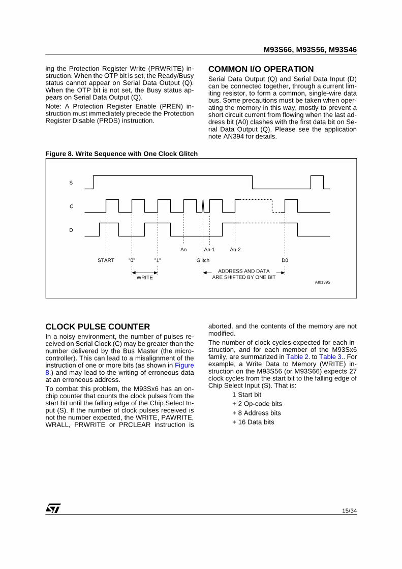
Figure 8. Write Sequence with One Clock Glitch
CLOCK PULSE COUNTERIn a noisy environment, the number of pulses re-ceived on Serial Clock (C) may be greater than thenumber delivered by the Bus Master (the micro-controller). This can lead to a misalignment of theinstruction of one or more bits (as shown in Figure8.) and may lead to the writing of erroneous dataat an erroneous address.To combat this problem, the M93Sx6 has an on-chip counter that counts the clock pulses from thestart bit until the falling edge of the Chip Select In-put (S). If the number of clock pulses received isnot the number expected, the WRITE, PAWRITE,WRALL, PRWRITE or PRCLEAR instruction is
aborted, and the contents of the memory are notmodified.The number of clock cycles expected for each in-struction, and for each member of the M93Sx6family, are summarized in Table 2. to Table 3.. Forexample, a Write Data to Memory (WRITE) in-struction on the M93S56 (or M93S66) expects 27clock cycles from the start bit to the falling edge ofChip Select Input (S). That is:
1 Start bit+ 2 Op-code bits+ 8 Address bits+ 16 Data bits
AI01395
S
An-1
C
D
WRITE
START D0"1""0"
An
Glitch
An-2
ADDRESS AND DATAARE SHIFTED BY ONE BIT

M93S66, M93S56, M93S46
16/34
MAXIMUM RATINGStressing the device above the rating listed in theAbsolute Maximum Ratings" table may cause per-manent damage to the device. These are stressratings only and operation of the device at these orany other conditions above those indicated in theOperating sections of this specification is not im-
plied. Exposure to Absolute Maximum Rating con-ditions for extended periods may affect devicereliability. Refer also to the STMicroelectronicsSURE Program and other relevant quality docu-ments.
Table 4. Absolute Maximum Ratings
Note: 1. Compliant with JEDEC Std J-STD-020B (for small body, Sn-Pb or Pb assembly), the ST ECOPACK® 7191395 specification, andthe European directive on Restrictions on Hazardous Substances (RoHS) 2002/95/EU
2. JEDEC Std JESD22-A114A (C1=100 pF, R1=1500 Ω, R2=500 Ω)
Symbol Parameter Min. Max. Unit
TSTG Storage Temperature –65 150 °C
TLEAD Lead Temperature during Soldering See note 1 °C
VOUT Output range (Q = VOH or Hi-Z) –0.50 VCC+0.5 V
VIN Input range –0.50 VCC+1 V
VCC Supply Voltage –0.50 6.5 V
VESD Electrostatic Discharge Voltage (Human Body model) 2 –4000 4000 V
17/34
M93S66, M93S56, M93S46
DC AND AC PARAMETERSThis section summarizes the operating and mea-surement conditions, and the DC and AC charac-teristics of the device. The parameters in the DCand AC Characteristic tables that follow are de-rived from tests performed under the Measure-
ment Conditions summarized in the relevanttables. Designers should check that the operatingconditions in their circuit match the measurementconditions when relying on the quoted parame-ters.
Table 5. Operating Conditions (M93Sx6)
Table 6. Operating Conditions (M93Sx6-W)
Table 7. Operating Conditions (M93Sx6-R)
Table 8. AC Measurement Conditions (M93Sx6)
Note: Output Hi-Z is defined as the point where data out is no longer driven.
Table 9. AC Measurement Conditions (M93Sx6-W and M93Sx6-R)
Note: Output Hi-Z is defined as the point where data out is no longer driven.
Symbol Parameter Min. Max. Unit
VCC Supply Voltage 4.5 5.5 V
TA
Ambient Operating Temperature (Device Grade 6) –40 85 °C
Ambient Operating Temperature (Device Grade 3) –40 125 °C
Symbol Parameter Min. Max. Unit
VCC Supply Voltage 2.5 5.5 V
TA Ambient Operating Temperature (Device Grade 6) –40 85 °C
Symbol Parameter Min. Max. Unit
VCC Supply Voltage 1.8 5.5 V
TA Ambient Operating Temperature (Device Grade 6) –40 85 °C
Symbol Parameter Min. Max. Unit
CL Load Capacitance 100 pF
Input Rise and Fall Times 50 ns
Input Pulse Voltages 0.4 V to 2.4 V V
Input Timing Reference Voltages 1.0 V and 2.0 V V
Output Timing Reference Voltages 0.8 V and 2.0 V V
Symbol Parameter Min. Max. Unit
CL Load Capacitance 100 pF
Input Rise and Fall Times 50 ns
Input Pulse Voltages 0.2VCC to 0.8VCC V
Input Timing Reference Voltages 0.3VCC to 0.7VCC V
Output Timing Reference Voltages 0.3VCC to 0.7VCC V
M93S66, M93S56, M93S46
18/34
Figure 9. AC Testing Input Output Waveforms
Table 10. Capacitance
Note: Sampled only, not 100% tested, at TA=25°C and a frequency of 1 MHz.
Symbol Parameter Test Condition Min Max Unit
COUT OutputCapacitance
VOUT = 0V5 pF
CIN InputCapacitance
VIN = 0V 5 pF
AI02791
2.4V
0.4V
2.0V
0.8V
2V
1V
INPUT OUTPUT
0.8VCC
0.2VCC
0.7VCC
0.3VCC
M93SXX-W & M93SXX-R
M93SXX

19/34
M93S66, M93S56, M93S46
Table 11. DC Characteristics (M93Sx6, Device Grade 6)
Note: 1. Current product: identified by Process Identification letter F or M.2. New product: identified by Process Identification letter W or G.
Table 12. DC Characteristics (M93Sx6, Device Grade 3)
Note: 1. Current product: identified by Process Identification letter F or M.2. New product: identified by Process Identification letter W or G.
Symbol Parameter Test Condition Min. Max. Unit
ILI Input Leakage Current 0V ≤ VIN ≤ VCC ±2.5 µA
ILO Output Leakage Current 0V ≤ VOUT ≤ VCC, Q in Hi-Z ±2.5 µA
ICC Supply Current
VCC = 5V, S = VIH, f = 1 MHz, Current
Product 1 1.5 mA
VCC = 5V, S = VIH, f = 2 MHz, New
Product 2 2 mA
ICC1 Supply Current (Stand-by)
VCC = 5V, S = VSS, C = VSS,
Current Product 1 50 µA
VCC = 5V, S = VSS, C = VSS,
New Product 2 15 µA
VIL Input Low Voltage VCC = 5V ± 10% –0.45 0.8 V
VIH Input High Voltage VCC = 5V ± 10% 2 VCC + 1 V
VOL Output Low Voltage VCC = 5V, IOL = 2.1mA 0.4 V
VOH Output High Voltage VCC = 5V, IOH = –400µA 2.4 V

M93S66, M93S56, M93S46
20/34
Table 13. DC Characteristics (M93Sx6-W, Device Grade 6)
Note: 1. Current product: identified by Process Identification letter F or M.2. New product: identified by Process Identification letter W or G.
Symbol Parameter Test Condition Min. Max. Unit
ILI Input Leakage Current 0V ≤ VIN ≤ VCC ±2.5 µA
ILO Output Leakage Current 0V ≤ VOUT ≤ VCC, Q in Hi-Z ±2.5 µA
ICCSupply Current (CMOS Inputs)
VCC = 5V, S = VIH, f = 1 MHz, Current
Product 1 1.5 mA
VCC = 2.5V, S = VIH, f = 1 MHz, Current
Product 1 1 mA
VCC = 5V, S = VIH, f = 2 MHz, New
Product 2 2 mA
VCC = 2.5V, S = VIH, f = 2 MHz, New
Product 2 1 mA
ICC1 Supply Current (Stand-by)
VCC = 2.5V, S = VSS, C = VSS,
Current Product 1 10 µA
VCC = 2.5V, S = VSS, C = VSS,
New Product 2 5 µA
VIL Input Low Voltage (D, C, S) –0.45 0.2 VCC V
VIH Input High Voltage (D, C, S) 0.7 VCC VCC + 1 V
VOL Output Low Voltage (Q) VCC = 5V, IOL = 2.1mA 0.4 V
VCC = 2.5V, IOL = 100µA 0.2 V
VOH Output High Voltage (Q) VCC = 5V, IOH = –400µA 2.4 V
VCC = 2.5V, IOH = –100µA VCC–0.2 V

21/34
M93S66, M93S56, M93S46
Table 14. DC Characteristics (M93Sx6-W, Device Grade 3)
Note: 1. New product: identified by Process Identification letter W or G.
Table 15. DC Characteristics (M93Sx6-R)
Note: 1. Preliminary Data: this product is under development. For more infomation, please contact your nearest ST sales office.
Symbol Parameter Test Condition Min 1. Max. 1 Unit
ILI Input Leakage Current 0V ≤ VIN ≤ VCC ±2.5 µA
ILO Output Leakage Current 0V ≤ VOUT ≤ VCC, Q in Hi-Z ±2.5 µA
ICCSupply Current (CMOS Inputs)
VCC = 5V, S = VIH, f = 2 MHz 2 mA
VCC = 2.5V, S = VIH, f = 2 MHz 1 mA
ICC1 Supply Current (Stand-by) VCC = 2.5V, S = VSS, C = VSS 5 µA
VIL Input Low Voltage (D, C, S) –0.45 0.2 VCC V
VIH Input High Voltage (D, C, S) 0.7 VCC VCC + 1 V
VOL Output Low Voltage (Q) VCC = 5V, IOL = 2.1mA 0.4 V
VCC = 2.5V, IOL = 100µA 0.2 V
VOH Output High Voltage (Q) VCC = 5V, IOH = –400µA 2.4 V
VCC = 2.5V, IOH = –100µA VCC–0.2 V
Symbol Parameter Test Condition Min. 1 Max. 1 Unit
ILI Input Leakage Current 0V ≤ VIN ≤ VCC ±2.5 µA
ILO Output Leakage Current 0V ≤ VOUT ≤ VCC, Q in Hi-Z ±2.5 µA
ICCSupply Current (CMOS Inputs)
VCC = 5V, S = VIH, f = 2 MHz 2 mA
VCC = 1.8V, S = VIH, f = 1 MHz 1 mA
ICC1 Supply Current (Stand-by) VCC = 1.8V, S = VSS, C = VSS 2 µA
VIL Input Low Voltage (D, C, S) –0.45 0.2 VCC V
VIH Input High Voltage (D, C, S) 0.8 VCC VCC + 1 V
VOL Output Low Voltage (Q) VCC = 1.8V, IOL = 100µA 0.2 V
VOH Output High Voltage (Q) VCC = 1.8V, IOH = –100µA VCC–0.2 V

M93S66, M93S56, M93S46
22/34
Table 16. AC Characteristics (M93Sx6, Device Grade 6 or 3)
Note: 1. tCHCL + tCLCH ≥ 1 / fC.2. Chip Select Input (S) must be brought Low for a minimum of tSLSH between consecutive instruction cycles.3. Current product: identified by Process Identification letter F or M.4. New product: identified by Process Identification letter W or G.
Test conditions specified in Table 8. and Table 5.
Symbol Alt. Parameter Min.3 Max.3 Min.4 Max.4 Unit
fC fSK Clock Frequency D.C. 1 D.C. 2 MHz
tPRVCH tPRES Protect Enable Valid to Clock High 50 50 ns
tWVCH tPES Write Enable Valid to Clock High 50 50 ns
tCLPRX tPREH Clock Low to Protect Enable Transition 0 0 ns
tSLWX tPEHChip Select Low to Write Enable Transition 250 250 ns
tSLCH Chip Select Low to Clock High 250 50 ns
tSHCH tCSS
Chip Select Set-up TimeM93C46, M93C56, M93C66
50 50 ns
Chip Select Set-up timeM93C76, M93C86
100 50 ns
tSLSH2 tCS Chip Select Low to Chip Select High 250 200 ns
tCHCL1 tSKH Clock High Time 250 200 ns
tCLCH1 tSKL Clock Low Time 250 200 ns
tDVCH tDIS Data In Set-up Time 100 50 ns
tCHDX tDIH Data In Hold Time 100 50 ns
tCLSH tSKS Clock Set-up Time (relative to S) 100 50 ns
tCLSL tCSH Chip Select Hold Time 0 0 ns
tSHQV tSV Chip Select to Ready/Busy Status 400 200 ns
tSLQZ tDF Chip Select Low to Output Hi-Z 200 100 ns
tCHQL tPD0 Delay to Output Low 400 200 ns
tCHQV tPD1 Delay to Output Valid 400 200 ns
tW tWP Erase/Write Cycle time 10 5 ms

23/34
M93S66, M93S56, M93S46
Table 17. AC Characteristics (M93Sx6-W, Device Grade 6)
Note: 1. tCHCL + tCLCH ≥ 1 / fC.2. Chip Select Input (S) must be brought Low for a minimum of tSLSH between consecutive instruction cycles.3. Current product: identified by Process Identification letter F or M.4. New product: identified by Process Identification letter W or G.
Test conditions specified in Table 9. and Table 6.
Symbol Alt. Parameter Min.3 Max.3 Min.4 Max.4 Unit
fC fSK Clock Frequency D.C. 1 D.C. 2 MHz
tPRVCH tPRES Protect Enable Valid to Clock High 50 50 ns
tWVCH tPES Write Enable Valid to Clock High 50 50 ns
tCLPRX tPREH Clock Low to Protect Enable Transition 0 0 ns
tSLWX tPEHChip Select Low to Write Enable Transition 250 250 ns
tSLCH Chip Select Low to Clock High 250 50 ns
tSHCH tCSS Chip Select Set-up Time 100 50 ns
tSLSH2 tCS Chip Select Low to Chip Select High 1000 200 ns
tCHCL1 tSKH Clock High Time 350 200 ns
tCLCH1 tSKL Clock Low Time 250 200 ns
tDVCH tDIS Data In Set-up Time 100 50 ns
tCHDX tDIH Data In Hold Time 100 50 ns
tCLSH tSKS Clock Set-up Time (relative to S) 100 50 ns
tCLSL tCSH Chip Select Hold Time 0 0 ns
tSHQV tSV Chip Select to Ready/Busy Status 400 200 ns
tSLQZ tDF Chip Select Low to Output Hi-Z 200 100 ns
tCHQL tPD0 Delay to Output Low 400 200 ns
tCHQV tPD1 Delay to Output Valid 400 200 ns
tW tWP Erase/Write Cycle time 10 5 ms

M93S66, M93S56, M93S46
24/34
Table 18. AC Characteristics (M93Sx6-W, Device Grade 3)
Note: 1. tCHCL + tCLCH ≥ 1 / fC.2. Chip Select Input (S) must be brought Low for a minimum of tSLSH between consecutive instruction cycles.3. New product: identified by Process Identification letter W or G.
Test conditions specified in Table 9. and Table 6.
Symbol Alt. Parameter Min.3 Max.3 Unit
fC fSK Clock Frequency D.C. 2 MHz
tPRVCH tPRES Protect Enable Valid to Clock High 50 ns
tWVCH tPES Write Enable Valid to Clock High 50 ns
tCLPRX tPREH Clock Low to Protect Enable Transition 0 ns
tSLWX tPEH Chip Select Low to Write Enable Transition 250 ns
tSLCH Chip Select Low to Clock High 50 ns
tSHCH tCSS Chip Select Set-up Time 50 ns
tSLSH2 tCS Chip Select Low to Chip Select High 200 ns
tCHCL1 tSKH Clock High Time 200 ns
tCLCH1 tSKL Clock Low Time 200 ns
tDVCH tDIS Data In Set-up Time 50 ns
tCHDX tDIH Data In Hold Time 50 ns
tCLSH tSKS Clock Set-up Time (relative to S) 50 ns
tCLSL tCSH Chip Select Hold Time 0 ns
tSHQV tSV Chip Select to Ready/Busy Status 200 ns
tSLQZ tDF Chip Select Low to Output Hi-Z 100 ns
tCHQL tPD0 Delay to Output Low 200 ns
tCHQV tPD1 Delay to Output Valid 200 ns
tW tWP Erase/Write Cycle time 5 ms
25/34
M93S66, M93S56, M93S46
Table 19. AC Characteristics (M93Sx6-R)
Note: 1. tCHCL + tCLCH ≥ 1 / fC.2. Chip Select Input (S) must be brought Low for a minimum of tSLSH between consecutive instruction cycles.3. Preliminary Data: this product is under development. For more infomation, please contact your nearest ST sales office.
Test conditions specified in Table 9. and Table 7.
Symbol Alt. Parameter Min.3 Max.3 Unit
fC fSK Clock Frequency D.C. 1 MHz
tPRVCH tPRES Protect Enable Valid to Clock High 50 ns
tWVCH tPES Write Enable Valid to Clock High 50 ns
tCLPRX tPREH Clock Low to Protect Enable Transition 0 ns
tSLWX tPEH Chip Select Low to Write Enable Transition 250 ns
tSLCH Chip Select Low to Clock High 250 ns
tSHCH tCSS Chip Select Set-up Time 50 ns
tSLSH2 tCS Chip Select Low to Chip Select High 250 ns
tCHCL1 tSKH Clock High Time 250 ns
tCLCH1 tSKL Clock Low Time 250 ns
tDVCH tDIS Data In Set-up Time 100 ns
tCHDX tDIH Data In Hold Time 100 ns
tCLSH tSKS Clock Set-up Time (relative to S) 100 ns
tCLSL tCSH Chip Select Hold Time 0 ns
tSHQV tSV Chip Select to Ready/Busy Status 400 ns
tSLQZ tDF Chip Select Low to Output Hi-Z 200 ns
tCHQL tPD0 Delay to Output Low 400 ns
tCHQV tPD1 Delay to Output Valid 400 ns
tW tWP Erase/Write Cycle time 10 ms

M93S66, M93S56, M93S46
26/34
Figure 10. Synchronous Timing (Start and Op-Code Input)
Figure 11. Synchronous Timing (Read or Write)
PRE
W
C
S
D OP CODE OP CODESTART
STARTOP CODE INPUT
tCHDXtDVCH
tCLSH tCLCH
tCHCLtWVCH
tPRVCH
AI02025
tSHCH
AI002026
C
D
Q
ADDRESS INPUT
Hi-Z
tDVCH
tCLSL
A0
S
DATA OUTPUT
tCHQVtCHDX
tCHQL
An
tSLSH
tSLQZ
Q15 Q0
27/34
M93S66, M93S56, M93S46
Figure 12. Synchronous Timing (Read or Write)
PRE
W
C
S
D
Hi-Z
tW
tDVCH
AI02027
Q
tCLPRX
tSLWX
tCLSL
tCHDX
tSLSH
tSLQZ
BUSY
tSHQV
READY
WRITE CYCLEADDRESS/DATA INPUT
An A0/D0
tSLCH
M93S66, M93S56, M93S46
28/34
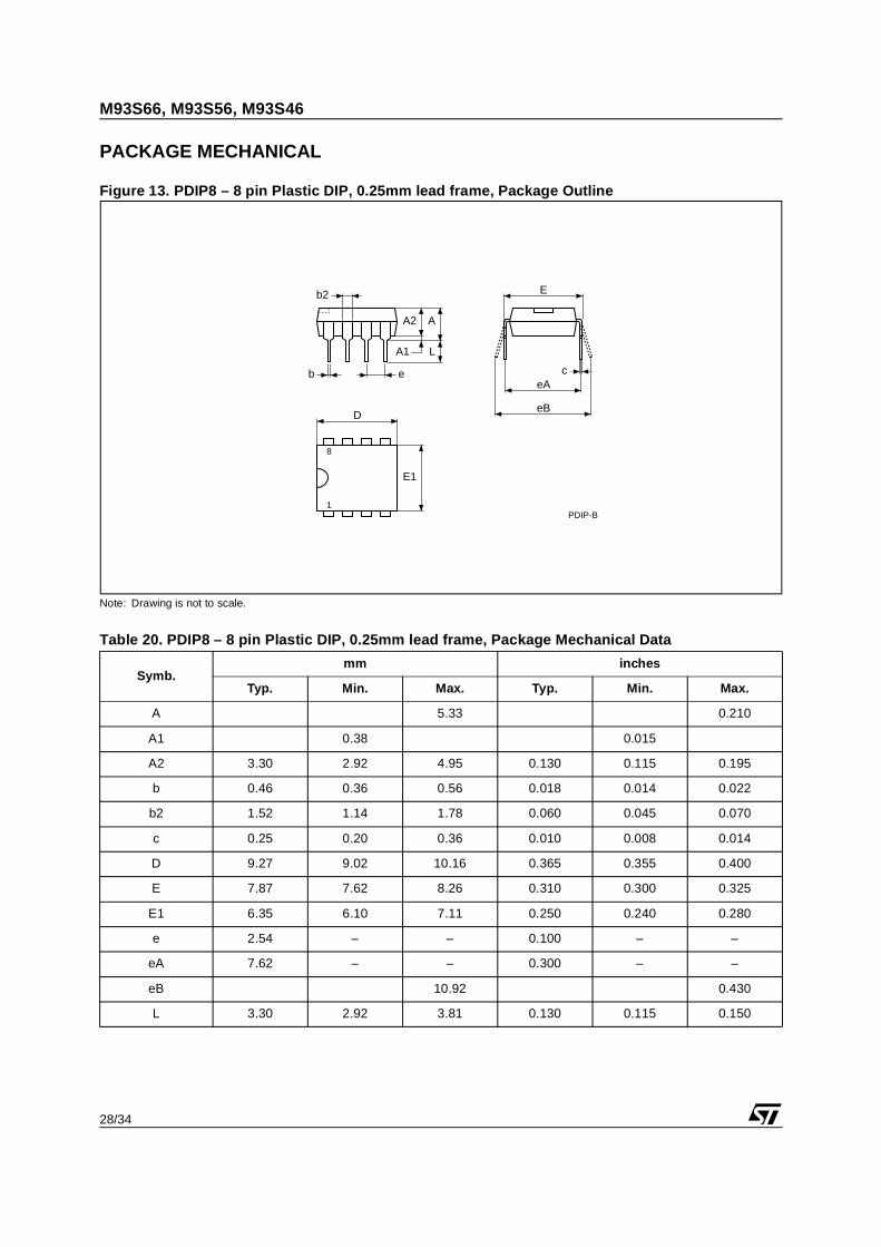
PACKAGE MECHANICAL
Figure 13. PDIP8 – 8 pin Plastic DIP, 0.25mm lead frame, Package Outline
Note: Drawing is not to scale.
Table 20. PDIP8 – 8 pin Plastic DIP, 0.25mm lead frame, Package Mechanical Data
Symb.mm inches
Typ. Min. Max. Typ. Min. Max.
A 5.33 0.210
A1 0.38 0.015
A2 3.30 2.92 4.95 0.130 0.115 0.195
b 0.46 0.36 0.56 0.018 0.014 0.022
b2 1.52 1.14 1.78 0.060 0.045 0.070
c 0.25 0.20 0.36 0.010 0.008 0.014
D 9.27 9.02 10.16 0.365 0.355 0.400
E 7.87 7.62 8.26 0.310 0.300 0.325
E1 6.35 6.10 7.11 0.250 0.240 0.280
e 2.54 – – 0.100 – –
eA 7.62 – – 0.300 – –
eB 10.92 0.430
L 3.30 2.92 3.81 0.130 0.115 0.150
PDIP-B
A2
A1
A
L
b e
D
E1
8
1
ceA
b2
eB
E
29/34
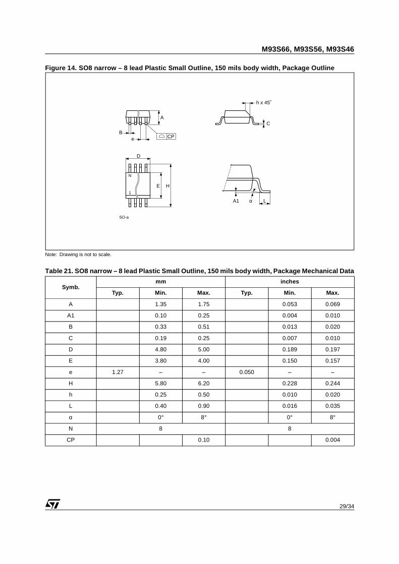
M93S66, M93S56, M93S46
Figure 14. SO8 narrow – 8 lead Plastic Small Outline, 150 mils body width, Package Outline
Note: Drawing is not to scale.
Table 21. SO8 narrow – 8 lead Plastic Small Outline, 150 mils body width, Package Mechanical Data
Symb.mm inches
Typ. Min. Max. Typ. Min. Max.
A 1.35 1.75 0.053 0.069
A1 0.10 0.25 0.004 0.010
B 0.33 0.51 0.013 0.020
C 0.19 0.25 0.007 0.010
D 4.80 5.00 0.189 0.197
E 3.80 4.00 0.150 0.157
e 1.27 – – 0.050 – –
H 5.80 6.20 0.228 0.244
h 0.25 0.50 0.010 0.020
L 0.40 0.90 0.016 0.035
α 0° 8° 0° 8°
N 8 8
CP 0.10 0.004
SO-a
E
N
CPB
e
A
D
C
LA1 α
1
H
h x 45˚
M93S66, M93S56, M93S46
30/34
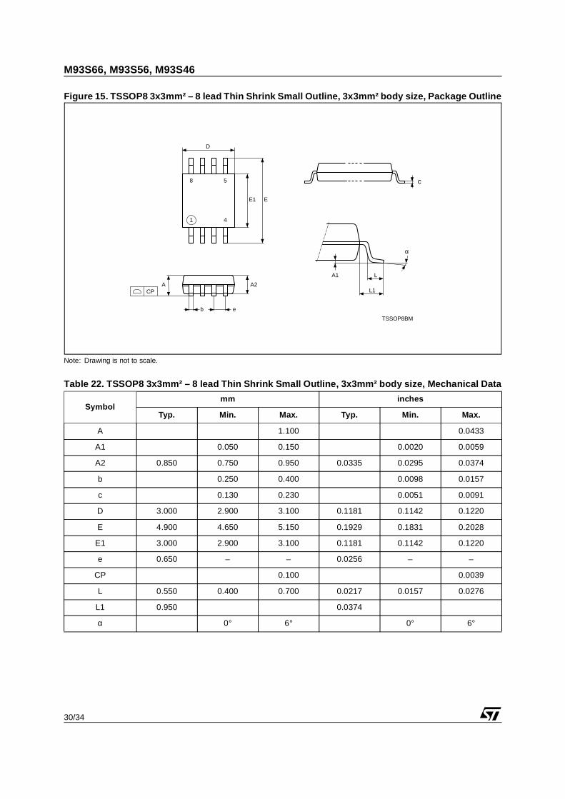
Figure 15. TSSOP8 3x3mm² – 8 lead Thin Shrink Small Outline, 3x3mm² body size, Package Outline
Note: Drawing is not to scale.
Table 22. TSSOP8 3x3mm² – 8 lead Thin Shrink Small Outline, 3x3mm² body size, Mechanical Data
Symbolmm inches
Typ. Min. Max. Typ. Min. Max.
A 1.100 0.0433
A1 0.050 0.150 0.0020 0.0059
A2 0.850 0.750 0.950 0.0335 0.0295 0.0374
b 0.250 0.400 0.0098 0.0157
c 0.130 0.230 0.0051 0.0091
D 3.000 2.900 3.100 0.1181 0.1142 0.1220
E 4.900 4.650 5.150 0.1929 0.1831 0.2028
E1 3.000 2.900 3.100 0.1181 0.1142 0.1220
e 0.650 – – 0.0256 – –
CP 0.100 0.0039
L 0.550 0.400 0.700 0.0217 0.0157 0.0276
L1 0.950 0.0374
α 0° 6° 0° 6°
TSSOP8BM
1
8
CP
c
L
EE1
D
A2A
α
eb
4
5
A1
L1
31/34
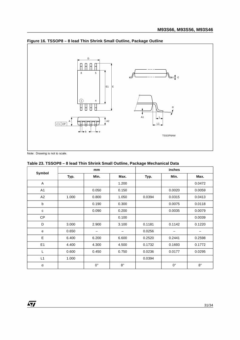
M93S66, M93S56, M93S46
Figure 16. TSSOP8 – 8 lead Thin Shrink Small Outline, Package Outline
Note: Drawing is not to scale.
Table 23. TSSOP8 – 8 lead Thin Shrink Small Outline, Package Mechanical Data
Symbolmm inches
Typ. Min. Max. Typ. Min. Max.
A 1.200 0.0472
A1 0.050 0.150 0.0020 0.0059
A2 1.000 0.800 1.050 0.0394 0.0315 0.0413
b 0.190 0.300 0.0075 0.0118
c 0.090 0.200 0.0035 0.0079
CP 0.100 0.0039
D 3.000 2.900 3.100 0.1181 0.1142 0.1220
e 0.650 – – 0.0256 – –
E 6.400 6.200 6.600 0.2520 0.2441 0.2598
E1 4.400 4.300 4.500 0.1732 0.1693 0.1772
L 0.600 0.450 0.750 0.0236 0.0177 0.0295
L1 1.000 0.0394
α 0° 8° 0° 8°
TSSOP8AM
1
8
CP
c
L
EE1
D
A2A
α
eb
4
5
A1
L1
M93S66, M93S56, M93S46
32/34
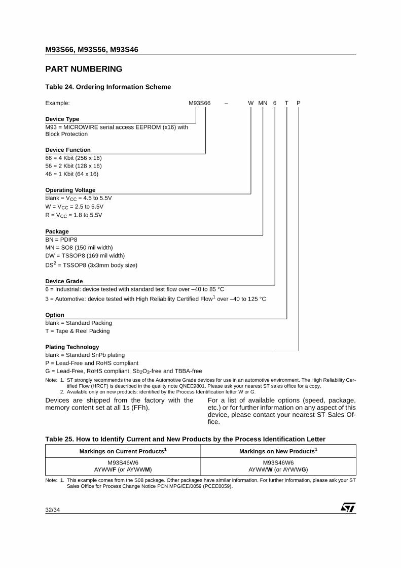
PART NUMBERING
Table 24. Ordering Information Scheme
Note: 1. ST strongly recommends the use of the Automotive Grade devices for use in an automotive environment. The High Reliability Cer-tified Flow (HRCF) is described in the quality note QNEE9801. Please ask your nearest ST sales office for a copy.
2. Available only on new products: identified by the Process Identification letter W or G.
Devices are shipped from the factory with thememory content set at all 1s (FFh).
For a list of available options (speed, package,etc.) or for further information on any aspect of thisdevice, please contact your nearest ST Sales Of-fice.
Table 25. How to Identify Current and New Products by the Process Identification Letter
Note: 1. This example comes from the S08 package. Other packages have similar information. For further information, please ask your STSales Office for Process Change Notice PCN MPG/EE/0059 (PCEE0059).
Example: M93S66 – W MN 6 T P
Device TypeM93 = MICROWIRE serial access EEPROM (x16) with Block Protection
Device Function66 = 4 Kbit (256 x 16)56 = 2 Kbit (128 x 16)46 = 1 Kbit (64 x 16)
Operating Voltageblank = VCC = 4.5 to 5.5V
W = VCC = 2.5 to 5.5VR = VCC = 1.8 to 5.5V
PackageBN = PDIP8MN = SO8 (150 mil width)DW = TSSOP8 (169 mil width)
DS2 = TSSOP8 (3x3mm body size)
Device Grade6 = Industrial: device tested with standard test flow over –40 to 85 °C
3 = Automotive: device tested with High Reliability Certified Flow1 over –40 to 125 °C
Optionblank = Standard PackingT = Tape & Reel Packing
Plating Technologyblank = Standard SnPb platingP = Lead-Free and RoHS compliantG = Lead-Free, RoHS compliant, Sb2O3-free and TBBA-free
Markings on Current Products1 Markings on New Products1
M93S46W6AYWWF (or AYWWM)
M93S46W6AYWWW (or AYWWG)

33/34
M93S66, M93S56, M93S46
REVISION HISTORY
Table 26. Document Revision History
Date Rev. Description of Revision
07-Mar-2002 2.0
Document reformatted, and reworded, using the new template. Temperature range 1 removed. TSSOP8 (3x3mm) package added. New products, identified by the process letter W, added, with fc(max) increased to 1MHz for -R voltage range, and to 2MHz for all other ranges (and corresponding parameters adjusted).
26-Mar-2003 2.1Value of standby current (max) corrected in DC characteristics tables for -W and -R rangesVOUT and VIN separated from VIO in the Absolute Maximum Ratings table
14-Apr-2003 2.2Values corrected in AC characteristics tables for -W range (tSLSH, tDVCH, tCLSL) for devices with Process Identification Letter W.
23-May-2003 2.3Standby current corrected for -R range. Four missing parameters restored to all AC Characteristics tables
24-Nov-2003 3.0 Table of contents, and Pb-free options added. VIL(min) improved to -0.45V.
19-Apr-2004 4.0Absolute Maximum Ratings for VIO(min) and VCC(min) changed. Soldering temperature information clarified for RoHS compliant devices. Device Grade 3 clarified, with reference to HRCF and automotive environments. Process identification letter “G” information added

M93S66, M93S56, M93S46
34/34
Information furnished is believed to be accurate and reliable. However, STMicroelectronics assumes no responsibility for the consequences of use of such information nor for any infringement of patents or other rights of third parties which may result from its use. No license is granted by implication or otherwise under any patent or patent rights of STMicroelectronics. Specifications mentioned in this publication are subject to change without notice. This publication supersedes and replaces all information previously supplied. STMicroelectronics products are not
authorized for use as critical components in life support devices or systems without express written approval of STMicroelectronics.
The ST logo is a registered trademark of STMicroelectronics.
All other names are the property of their respective owners.
© 2004 STMicroelectronics - All rights reserved
STMicroelectronics GROUP OF COMPANIESAustralia - Belgium - Brazil - Canada - China - Czech Republic - Finland - France - Germany -
Hong Kong - India - Israel - Italy - Japan - Malaysia - Malta - Morocco - Singapore -Spain - Sweden - Switzerland - United Kingdom - United States
www.st.com