Embed Size (px)
Citation preview

97-33
8- P N89 - 1945 8 I TDA Progress Report 42-96 October- December 1988
On Testing VLSI Chips for the Big Viterbi Decoder I. S. Hsu
Communicat ions Systems Research Section
A general technique that can be used in testing velyaargetcaldntegrated (VLSI) chips for the Big Viterbi Decoder (BVD) system is described,i+&kwtkk. The test tech- nique is divided into functional testing and fault-coverage testing. The purpose of func- tional testing is to verify that the design works functionally. Functional test vectors are converted from outputs of software simulations which simulate the B VD functionally. Fault-coverage testing is used to detect and, in some cases, to locate faulty components caused by bad fabrication. This type of testing is useful in screening out bad chips. Fin- a&, ‘design for testabilit-v,’ which is included in the BVD VLSI chip design, is described in considerable detail in this article. Both the observability and controllability of a VLSI chip are greatly enhanced by including the design for testability feature.
1. Introduction A concatenated system which uses a (255,223) Reed-
Solomon outer code and a (7,1/2) Viterbi-decoded con- volutional inner code has been recommended by the Consul- tative Committee for Space Data Systems (CCSDS) [ l ] as a standard channelcoding scheme for the future DSN. This concatenated scheme will provide an additional 2 dB in coding gain at a bit error rate (BER) of over a Viterbi-decoded- only channel [ 2 ] . However, there is a need for even greater coding gain in future missions such as Galileo. A recent JPL Research and Technology Objectives and Plans (RTOP) activity showed that an additional 2 dB coding gain over.the concatenated coding channel recommended by CCSDS can be achieved by concatenating a (1023,959) Reed-Solomon code with a (15,1/6) Viterbi-decoded convolutional code [3] ,
A VLSI-based BVD for convolutional codes is described in [4] . It will be able to decode convolutional codes with con- straint length K from 1 to 15 and code rate varying from 1/2
to 1/6. The difficulty in building the BVD is the large number of states in the Viterbi decoding algorithm [ti], which grow exponentially with K . For example, there are 2 l4 states in a (15,1/6) Viterbi decoder. These 214 states can be configured as 2 l3 butterflies, each butterfly consisting of two states. Each state performs add, compare, and select operations [4] with an operation speed of 1 Mbit/sec. Implementing such a large number of butterflies in silicon with current technology is an extremely difficult task.
Bit-serial arithmetic is used in the BVD [4] to simplify the complexity caused by the large number of states. It is shown in [3] that the 2 l3 butterflies in the (15,1/6) Viterbi decoder can be implemented with 512 identical VLSI chips using 1.5-pm complementary-metal-oxide-semiconductor (CMOS) technology. Each chip contains 16 butterflies. It is estimated that each chip will contain about 20,000 gates where a gate corresponds to a standard two-input CMOS NotAnd (NAND) gate which contains four transistors. Because of the large
80
https://ntrs.nasa.gov/search.jsp?R=19890010087 2020-03-22T10:51:46+00:00Z

number of gates, the implementation of this chip must be carefully planned and should include a comprehensive testing strategy.
Testing of VLSI chips can be divided into functional test- ing and fault coverage testing. Functional testing verifies that the VLSI design functions as expected. The fault-coverage test is used to detect and, in some cases, to locate faulty compo- nents on a fabricated VLSI chip. Diagnostic procedures are carried out to determine if the faulty components are caused by bad fabrication or design errors. The detected errors can be corrected in a subsequent fabrication run if a design prob- lem is found.
This article describes a testing technique that will be used in developing the BVD VLSI chip. A tutorial on fault simula- tion and design for testability is also provided. In Section 11, the planned functional testing procedure for the (15,1/6) VLSI-based Viterbi decoder is described. Section I11 describes techniques that can be used for faultcoverage testing. Several techniques to increase design for testability of a VLSI chip are illustrated in Section IV in considerable detail. The tech- nique used to enhance design for testability of the BVD VLSI chips is described in Section V. Finally, some concluding remarks are made in Section VI.
II. Functional Testing of VLSl Chips The Big Viterbi Decoder system utilizes bit-serial arithmetic
t o reduce the complexity as well as increase operational speed of the VLSI chip [4 ] . In order to implement the 213 butter- flies in the BVD system with current 1.5-pm CMOS technol- ogy, 512 identical VLSI chips are required. Each VLSI chip contains 16 butterflies; each butterfly contains two states. Figure 1 shows the functional diagram of the BVD and Fig. 2 depicts a block diagram of a butterfly. Figure 3 shows a logic diagram of the metric computation unit in a butterfly.
A software simulator has been written to mimic the opera- tion of the bit-serial BVD hardware [6] . The outputs of the software simulator are converted into functional test vectors for the BVD VLSI chips. The following example illustrates the procedure of generating the functional test vectors. In Fig. 4, which depicts a sample software simulator output, ri (received messages) are represented in octal numbers. Thus, ri equals 227 in octal and 100101 11 in binary representation. Also in Fig, 4 , “label” denotes the identification of a butterfly [6], p and q represent the branch metrics computed from the corresponding received messages ri , x is the sum of magnitudes of the received symbols, mio, mjo are the old accumulated metrics, and mil , mil are the new accumulated metrics of the two states in the butterfly. Based on the outputs of the soft- ware simulator, functional test vectors for the metric compu- tation unit are generated. These functional test vectors are
manually entered into the VAX computer using a program called “Logic,” developed at JPL.1 The output files gen- erated by “Logic” are in “rsim”2 format which is widely used to represent logic vectors in university-based VLSI CAD systems. Both the system hardware and VLSI designs of the BVD are performed with the Valid workstation [7] . A transla- tor called “RSIM2VAL,”3 also developed at JPL, is used to convert the output of “Logic” to a format that is acceptable to the Valid logic simulator.
A hierarchical approach [8] is used in designing BVD chips. For example, after full logic simulation of the branch metric computation unit (Fig. 3), functional test vectors are gener- ated for testing combined blocks such as the branch metric and add/compare/select blocks depicted in Fig. 3. This process continues until functional testing of the entire chip is achieved.
After the VLSI chip layout passes logic simulations, circuit simulations, and design rule checking, it is ready to be shipped to the foundry for further checking procedures. For the BVD design, the foundry will perform fault simulation and some other check procedures to ensure that the VLSI chip design is error free. After the VLSI chip layout passes all the checking procedures by the foundry, it is ready for fabrication.
111. Techniques for Fault-Coverage Test of VLSl Chips
CMOS has been chosen as the fabrication technology for the VLSI chips in the BVD. Recently CMOS has been widely used because of its low power consumption, high density, high performance, and mature fabrication technology. The faults that most frequently occur in a CMOS circuit can be catego- rized into the following types:
(1) stuck-at-I fault
( 2 ) stuck-at4 fault
(3) stuck-open fault
(4) stuck-short fault
’L. J. Deutsch, “Logic - Simulate and Test VLSI Circuits,” Documen- tation of 1985 VLSl Tools (internal document), Communications Systems Research Section, Jet Propulsion Laboratory, Pasadena, California, 1985.
‘L. J. Deutsch, “rsim - a Superset of the rnl Simulator with File Input,” Documentation of 1985 VLSI Tools (internal document), Communi- cations System Research Section, Jet Propulsion Laboratory, Pasa- dena, California, 1985.
3L. J. Deutsch, “rsim2val - a translator from rsim format to Valid format,” Documentation of 1987 VLSl Tools (internal document), Communications Systems Research Section, Jet Propulsion Labora- tory, Pasadena, California, 1987.
81

The stuck-at-1 fault refers to a specific node in the chip that is always stuck at logic level 1 regardless of the input conditions. The stuck-at-0 fault, on the contrary, means that the node is always at logic level 0. The stuck-open fault indicates that a driving transistor is always open in spite of the change of the input voltage applied to it. This fault may be caused by an oxide-layer imperfection created during fabrica- tion or a faulty gate contact [9]. The stuck-short fault is the opposite effect. The transistor is always shorted regardless of the input voltage applied to the transistor. T h s fault is either due to pin holes created in the oxide layer during fabrication or the “punch-through’’ effect caused by excessive voltage applied to the drain terminal of the transistor [9]. Both the
simulate because time-delay effects are introduced by these faults. A combinational circuit is changed into a sequential circuit by the time-delay effect. There is no good method developed so far to simulate sequential circuits for fault- coverage. Fortunately, most of the stuck-open and stuck-short faults are covered by the stuck-at-1 and stuck-at-0 faults [ l o ] . Therefore, the stuck-open and stuck-short fault models are not mandatory. It has been reported that only 0.1 percent to 0.3 percent of the VLSI chips might have an undetected de- fect after passing test screens based on stuck-at fault only analysis [ l o ] .
I stuck-open and stuck-short faults are difficult to model and
Most of the existing VLSI fault-simulation programs deal with gate-level design. The fault simulation procedure can be divided into the following steps:
(1) Fault collapsing
(2) Test vector generation
(3) Fault simulation
After the logic schematic of a VLSI circuit is entered into the computer system, the fault simulator will perform fault collapsing. Given a combinational circuit, fault collapsing provides a number of fault classes. Each class consists of two fault sets: an equivalent set and a dominating set. Any test vector that can detect any one fault in an equivalent set will be able to detect all other faults in the same set. Any test vector that detects a fault in the equivalent set will also detect all the faults in the corresponding dominating set. However, it is not true that any test vectors that detect a fault in the domi- nating set will detect all the faults in the corresponding equiva- lent set.
For example, suppose there are N faults in a specific equiva- lent set and there are M faults in its corresponding dominant set. A test vector that detects a fault in the equivalent set will be able to detect all the other N - 1 faults in the same set. The M faults in the dominant set will also be detected by this parti-
cular test vector. Therefore, a test vector in the equivalent set can detect N t M faults by the faultcollapsing technique. It requires N t M test vectors to test these N t M faults without fault collapsing. Hence, the number of test vectors required for fault simulating a VLSI circuit is reduced substantially by per- forming fault collapsing.
Test vector generation provides test vectors for a given detectable fault based on a given logic design. Several software programs are available for generating test vectors, such as the program “PODEM” written at the University of Nebraska, Lincoln [l 11 . The resulting test vectors are then applied to the circuit for fault simulation. The purpose of running fault simu- lation is to identify all detectable faults by a given test vector. The errors at the outputs of the circuit caused by a specific cir- cuit fault with the applied input test vectors are obtained after fault simulation. By this means, a faulty transistor or connec- tion is easily detected and in some cases located.
The output from fault simulation is fault-coverage percent- age. Faultcoverage percentage is defined as the number of faults tested divided by the total number of possible faults. Usually, it is extremely difficult to achieve 100 percent fault coverage in a VLSI circuit, i.e ., t o detect all the possible faults. If there are undetectable faults, the designer can modify the logic design to reduce logic redundancy. Logic redundancy is the primary reason for not being able to achieve 100 percent fault coverage. Typically, it takes a long time to modify the logic design of a VLSI circuit to reduce logic redundancy. Consequently, a 98 percent fault coverage is normally accept- able for most VLSI designs [ 121 .
IV. Design for Testability Due to recent advancements in VLSI technology, a VLSI
chip can contain hundreds of thousands of transistors. The testing of such VLSI chips has become unmanageable with conventional testing schemes, and design for testability has gained increasing importance. The purpose of design for test- ability is to achieve 100 percent of “observability” and “con- trollability” of a VLSI circuit. Observability means that a given node in the circuit is observable from the outside envi- ronment. Controllability means that a given node in the circuit is controllable from the outside environment. Design for testability techniques are divided into two categories: the ad hoc approach and the structured approach. Ad hoc techniques solve a problem for a specific design but are not applicable to all designs. Structured techniques are applicable in general but certain design rules are required by which a design is imple- mented. In the following, general techniques for design for testability are briefly reviewed. For a more detailed descrip- tion, see [IS].
82
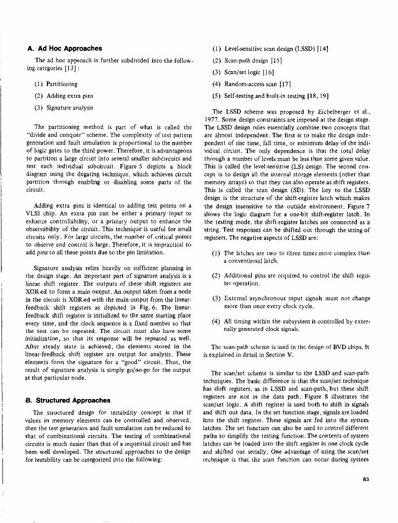
A. Ad Hoc Approaches
ing categories [ 131 : The ad hoc approach is further subdivided into the follow-
(1 ) Level-sensitive scan design (LSSD) [ 141
( 2 ) Scan-path design [ 151
(3) Scan/set logic [ 161
(4) Random-access scan [ 171
(5) Self-testing and built-in testing [18, 191
(1) Partitioning
( 2 ) Adding extra pins
(3) Signature analysis
The partitioning method is part of what is called the “divide and conquer” scheme. The complexity of test pattern generation and fault simulation is proportional to the number of logic gates t o the third power. Therefore, it is advantageous to partition a large circuit into several smaller subcircuits and test each individual subcircuit. Figure 5 depicts a block diagram using the degating technique, which achieves circuit partition through enabling or disabling some parts of the circuit.
Adding extra pins is identical to adding test points on a VLSI chip. An extra pin can be either a primary input to enhance controllability, or a primary output to enhance the observability of the circuit. This technique is useful for small circuits only. For large circuits, the number of critical points to observe and control is large. Therefore, it is impractical to add pins to all these points due to the pin limitation.
Signature analysis relies heavily on sufficient planning in the design stage. An important part of signature analysis is a linear shift register. The outputs of these shift registers are XORed to form a main output. An output taken from a node in the circuit is XORed with the main output from the linear- feedback shift registers as depicted in Fig. 6. The linear- feedback shift register is initialized to the same starting place every time, and the clock sequence is a fixed number so that the test can be repeated. The circuit must also have some initialization, so that its response will be repeated as well. After steady state is achieved, the elements stored in the linear-feedback shift register are output for analysis. These elements form the signature for a “good” circuit. Thus, the result of signature analysis is simply go/no-go for the output at that particular node.
6. Structured Approaches
The structured design for testability concept is that if values in memory elements can be controlled and observed, then the test generation and fault simulation can be reduced to that of combinational circuits. The testing of combinational circuits is much easier than that of a sequential circuit and has been well developed. The structured approaches to the design for testability can be categorized into the following:
The LSSD scheme was proposed by Eichelberger et al., 1977. Some design constraints are imposed at the design stage. The LSSD design rules essentially combine two concepts that are almost independent. The first is to make the design inde- pendent of rise time, fall time, or minimum delay of the indi- vidual circuit. The only dependence is that the total delay through a number of levels must be less than some given value. This is called the level-sensitive (LS) design. The second con- cept is t o design all the internal storage elements (other than memory arrays) so that they can also operate as shift registers. This is called the scan design (SD). The key to the LSSD design is the structure of the shift-register latch which makes the design insensitive to the outside environment. Figure 7 shows the logic diagram for a one-bit shift-register latch. In the testing mode, the shft-register latches are connected as a string. Test responses can be shifted out through the string of registers. The negative aspects of LSSD are:
(1) The latches are two to three times more complex than a conventional latch.
( 2 ) Additional pins are required to control the shift regis- ter operation.
(3) External asynchronous input signals must not change more than once every clock cycle.
(4) All timing within the subsystem is controlled by exter- nally generated clock signals.
The scan-path scheme is used in the design of BVD chips. It is explained in detail in Section V.
The scanlset scheme is similar to the LSSD and scan-path techniques. The basic difference is that the scan/set technique has shift registers, as in LSSD and scan-path, but these shift registers are not in the data path. Figure 8 illustrates the scan/set logic. A shift register is used both to shift in signals and shift out data. In the set function stage, signals are loaded into the shift register. These signals are fed into the system latches. The set function can also be used to control different paths to simplify the testing function. The contents of system latches can be loaded into the shift register in one clock cycle and shifted out serially. One advantage of using the scan/set technique is that the scan function can occur during system
83
operation since the shift register is external to the system circuit.
The purpose of the random-access scan is to have complete observability and controllability, the same as for the previous schemes. There are no shift registers needed in the random- access scan scheme. An addressing scheme which allows each latch to be uniquely selected is required instead. The address- ing scheme is similar to that of a random-access memory.
Figure 9 shows the system configuration of the random- access scan network. Any point in the combinational network can be observed with some additional logic gates. Figure 10 depicts a basic type of latch (labelled ‘‘RA Latch” in Fig. 9) required in the random-access scan technique. In Fig. 10, Yi, Qi and CK are used in normal operation where Yi is the output from the combinational circuit, Qi is an input to the circuit and CK is the system clock. SDI is the scan-data input, TCK is the clock used in the testing period to scan in data, and Select i controls the i th latch to be accessed. The Select i sig- nal is generated by decoding address inputs. By design, at most one of the Select i signals is equal to 1 at a time. Therefore, data are scanned into and out of the latches serially by a suit- able combination of the TCK and Select i signals. The outputs of the RA latches are wired together since only one RA latch output is valid at a time controlled by the Select i signal.
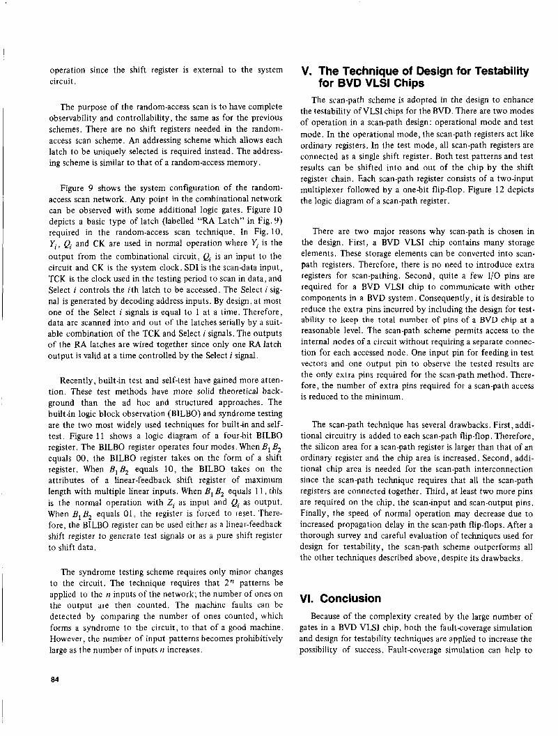
Recently, built-in test and self-test have gained more atten- tion. These test methods have more solid theoretical back- ground than the ad hoc and structured approaches. The built-in logic block observation (BILBO) and syndrome testing are the two most widely used techniques for built-in and self- test. Figure 11 shows a logic diagram of a four-bit BILBO register. The BILBO register operates four modes. When B, B, equals 00, the BILBO register takes on the form of a shift register. When B,B, equals 10, the BILBO takes on the attributes of a linear-feedback shift register of maximum length with multiple linear inputs. When B, B, equals 11, this is the normal operation with Zi as input and Qi as output. When BIB, equals 01, the register is forced to reset. There- fore, the BILBO register can be used either as a linear-feedback shift register to generate test signals or as a pure shift register to shift data.
The syndrome testing scheme requires only minor changes to the circuit. The technique requires that 2“ patterns be applied to the n inputs of the network; the number of ones on the output are then counted. The machine faults can be detected by comparing the number of ones counted, which forms a syndrome to the circuit, to that of a good machine. However, the number of input patterns becomes prohibitively large as the number of inputs n increases.
V. The Technique of Design for Testability for BVD VLSI Chips
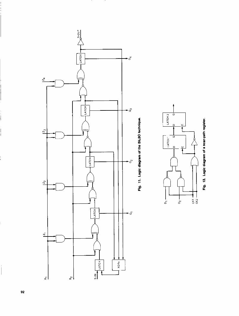
The scan-path scheme is adopted in the design to enhance the testability of VLSI chips for the BVD. There are two modes of operation in a scan-path design: operational mode and test mode. In the operational mode, the scan-path registers act like ordinary registers. In the test mode, all scan-path registers are connected as a single shift register. Both test patterns and test results can be shifted into and out of the chip by the shift register chain. Each scan-path register consists of a two-input multiplexer followed by a one-bit flip-flop. Figure 12 depicts the logic diagram of a scan-path register.
There are two major reasons why scan-path is chosen in the design. First, a BVD VLSI chip contains many storage elements. These storage elements can be converted into scan- path registers. Therefore, there is no need to introduce extra registers for scan-pathing. Second, quite a few 1/0 pins are required for a BVD VLSI chip to communicate with other components in a BVD system. Consequently, it is desirable to reduce the extra pins incurred by including the design for test- ability to keep the total number of pins of a BVD chip at a reasonable level. The scan-path scheme permits access to the internal nodes of a circuit without requiring a separate connec- tion for each accessed node. One input pin for feeding in test vectors and one output pin to observe the tested results are the only extra pins required for the scan-path method. There- fore, the number of extra pins required for a scan-path access is reduced to the minimum.
The scan-path technique has several drawbacks. First, addi- tional circuitry is added to each scan-path flip-flop. Therefore, the silicon area for a scan-path register is larger than that of an ordinary register and the chip area is increased. Second, addi- tional chip area is needed for the scan-path interconnection since the scan-path technique requires that all the scan-path registers are connected together. Third, at least two more pins are required on the chip, the scan-input and scan-output pins. Finally, the speed of normal operation may decrease due to increased propagation delay in the scan-path flip-flops. After a thorough survey and careful evaluation of techniques used for design for testability, the scan-path scheme outperforms all the other techniques described above, despite its drawbacks.
VI. Conclusion Because of the complexity created by the large number of
gates in a BVD VLSI chip, both the faultcoverage simulation and design for testability techniques are applied to increase the possibility of success. Faultcoverage simulation can help to
84

I
detect and, in some cases, to locate the faulty components on a VLSI chip. The design for testability scheme increases both the controllability and observability of a complex chip. A tutorial on faultcoverage simulation and design for testability
is given in this article. The scan-path technique is used in the BVD VLSI chip design because the area overhead incurred is small and a satisfactory performance is achieved at the same time.
I I
References I
[ 11 “Recommendation for Deep Space Data System Standards: Telemetry Channel Coding,” (Blue Book), Consultative Committee for Space Data Systems, CCSDS Secretariat, Communications and Data Systems Division, Code TS, NASA, Washing- ton, D.C., May 1984.
[2] R. L. Miller, L. J . Deutsch, and S. A. Butman, On the Error Statistics of Viterbi Decoding and the Performance of Concatenated Codes, JPL Publication 8 1-9, Jet Propulsion Laboratory, Pasadena, California, pp. 33-39, September 1, 1981.
[3] J. H. Yuen and Q . D. Vo, “In Search of a 2-dB Coding Gain,” TDA Progress Report 42-83, vol. July-September 1985, Jet Propulsion Laboratory, Pasadena, California, pp. 26-33, November 15, 1985.
[4] J. Statman, G. Zimmerman, F. Pollara, and 0. Collins, “A Long Constraint Length VLSI Viterbi Decoder for the DSN,” TDA Progress Report 42-95, vol. July- September 1988, Jet Propulsion Laboratory, Pasadena, California, pp. 134-142, November 15, 1988.
[5] A. J. Viterbi, “Convolutional Codes and Their Performance in Communication Sys- tems,” IEEE Trans. on Communications, vol. COM-19, no. 5, pt. 2, pp. 751-772, October 1971.
[ 6 ] S. Arnold and F. Pollara. “A Software Simulation Study of the Long Constraint Length VLSI Viterbi Decoder,” TDA Progress Report 42-94. vol. April-June 1988, Jet Propulsion Laboratory, Pasadena. California. pp. 210-221, August 15, 1988.
[7] “User’s Guide for the Scald Star System,” Valid Logic Systems, Inc., San Jose, CA 95134,1987.
[8] C. Mead and L. Conway, An Introduction to VLSISystem Design, Reading, Massa-
[9] A. B. Glaser and G. E. Subak-Sharpe, Integrated Circuit Engineering, Reading,
[ l o ] T. W. Williams and K. P. Parker, “Testing Logic Networks and Design for Testabil-
[ I 13 P. Goel, “An Implicit Enumeration Algorithm to Generate Tests for Combinational
[12] P. H. Bardell, W. H. McAnney, and J. Savir, Built-In Test for VLSI, New York:
[ 131 H. J . Nadig, “Signature Analysis, Concepts, Examples, and Guidelines,” Hewlett-
chusetts: Addison-Wesley, 1979.
Massachusetts: Addison-Wesley , 1978.
ity,” Computer, pp. 9-21, October 1979.
Logic Circuits,” IEEE Trans. on Computers, vol. C-30, pp. 21 5-222, March 1981.
John Wiley & Sons, 1987.
Packard J . , pp. 15-2 1, May 1977.
85

[14] S . Das Gupta, E. B. Eichelberger, and T. W. Williams, “LSI Chip Design for Testa- bility,” Digest Technical Papers, pp. 216-217, 1978 International Solid-state Circuit Conference, San Francisco, California.
[I51 S . Funastu, N. Wakatsuki, and T. Arima, “Test Generation Systems in Japan,” Proc. 12th Design Automation Symp., pp. 114-122, June 1975.
[16] J. H. Stewart, “Future Testing of Large LSI Circuit Cards,” Digest Papers, pp. 6-17, 1977 Semiconductor Test Symposium, IEEE Publication 77CH1261-7C, October 1977.
[I71 H. Ando, “Testing VLSI with Random-Access Scan,” Digest Papers, pp. 50-52,
[18] B. Koenemann, J . Mucha, and G. Zwiehoff, “Build-in Logic Observation Tech- niques,” Digest Papers, pp. 37-41, 1979 Test Conference, IEEE Publication 79CH1509-9C, October 1979.
Compcon 80, IEEE Publication 80CH1491-OC, February 1980.
[ 191 J . Savir, “Syndrome - Testing of Syndrome-Untestable Combinational Circuits,” IEEE Trans. on Computers, vol. C-29, pp. 442-45 1, June 1980.
I I
I 86

FRONT SCSI/ CRT/KBD PANEL TCT TPA GPlB
I COMPUTE R/MON I T 0 R/CONTRO L I
EXTERNAL - INPUT NODE SYNCH
ASSEMBLY t- E RASU R E PROCESS0 R
I ,=I-
COMPARATOR ASSEMBLY
SIMULATOR ASSEMB LY
I I
Fig. 1. Functional diagram of the Big Viterbi Decoder.
ADD/COMPARE/SE LECT
1 t l -
I I CONTROL/STATUS
- I BRANCH METRIC COMPUTER SYMBOLS
M ~ M C
OUT METRIC 0 + OUT METRIC 1 1---
3Y
Fig. 2. Block diagram of a butterfly.
87

IN
bo0 SERIAL-PARALLEL SHIFT REGISTER
9 0
t OUT
Fig. 3. Logic diagram of the branch metric computation unit.
88

r[O]= 227 r[1]= 227 r[2]= 227 r[3]= 227 r[4]= 227 r[5]= 227 s t a t e = 0 minmetric= 0 state= 0 maxmetric= 0 bit-no= 0 p= 212 q= 0 x= 212 b u t t = 0 l abe l= 0 miO= 0 mil= 0 mj0= 0 mjl= 0 p= 105 q= 105 x= 212 b u t t = 1 l abe l= 70 miO= 0 mil= 0 mj0=105 mjl=105 p= 105 q= 105 x= 212 b u t t = 2 l abe l= 34 miO= 0 mil= 0 mj0=105 mjl=105 p= 134 q= 56 x= 212 b u t t = 3 l abe l= 44 miO= 0 mil= 0 mjO= 56 mjl= 56 p= 56 q= 134 x= 212 but t= 4 l abe l= 66 miO= 0 mil= 0 mj0= 56 mjl= 56 p= 105 q= 105 x= 212 b u t t = 5 l abe l= 16 miO= 0 mil= 0 mj0=105 mjl=105 p= 105 q= 105 x= 212 b u t t = 6 l abe l= 52 miO= 0 mil= 0 mj0=105 mjl=105 p= 134 q= 56 x= 212 b u t t = 7 l abe l= 22 miO= 0 mil= 0 mj0= 56 mjl= 56 p= 27 q= 163 x= 212 b u t t = 8 l abe l= 37 miO= 0 mil= 0 mj0= 27 mjl= 27 p= 56 q= 134 x= 212 b u t t = 9 l abe l= 41 miO= 0 mil= 0 mj0= 56 mjl= 56 p= 134 q= 56 x= 212 b u t t = 10 l abe l= 3 miO= 0 mil= 0 mj0= 56 mjl= 56 p= 27 q= 163 x= 212 b u t t = 11 l abe l= 73 miO= 0 mil= 0 mj0= 27 mjl= 27 p= 105 q= 105 x= 212 b u t t = 12 l abe l= 51 miO= 0 mil= 0 mj0=105 mjl=105 p= 134 q= 56 x= 212 b u t t = 13 l abe l= 21 miO= 0 mil= 0 mj0= 56 mjl= 56 p= 56 q= 134 x= 212 b u t t = 14 l abe l= 65 miO= 0 mil= 0 mj0= 56 mjl= 56 p= 105 q= 105 x= 212 but t= 15 l abe l= 15 miO= 0 mil= 0 mj0=105 mjl=105 p= 105 q= 105 x= 212 but t= 16 l abe l= 32 miO= 0 mil= 0 mj0=105 mjl=105 p= 134 q= 56 x= 212 but t= 17 l abe l= 42 miO= 0 mil= 0 mj0= 56 mjl= 56 p= 134 q= 56 x= 2 1 2 b u t t = 18 label= 6 miO= 0 mil= 0 mj0= 56 mjl= 56 p= 27 q= 163 x= 212 b u t t = 19 l abe l= 76 miO= 0 mil= 0 mj0= 27 mjl= 27 p= 105 q= 105 x= 212 b u t t = 20 l abe l= 54 miO= 0 mil= 0 mj0=105 mjl=105 p= 134 q= 56 x= 212 b u t t = 21 l abe l= 24 miO= 0 mil= 0 mj0= 56 mjl= 56 p= 134 q= 56 x= 212 b u t t = 22 l abe l= 60
Fig. 4. Output from a BVD software simulator.
89

MODULE 1 L DEGATE
MODULE 2
I
L1 D
C
I
A L2
B Fig. 5. Block diagram of the degating technique.
Fig. 7. Logic diagram of a one-bit LSSD shift-register latch.
K CI RCUlT
Fig.
N-BIT SHIFT
-.)
- CIRCUIT CIRCUIT
6. Block diagram of the signatureanalysis CIRCUIT
technique. INPUT
Fig. 8. Block diagram of the scantset technique.
90

CIRCUIT INPUT
COMBINATIONAL CIRCUIT
CIRCUIT OUTPUT
l I
sELEcTi7 ? LATCH
A S D O
Fig. 9. Configuration of the random-access scan network.
"i
I SELECT i
t Fig. 10. Logic diagram of a random-access
scan latch.
91
@- A
p I , , f v)
5
a 0 a a 0 E 2
5
.c
8
92