Embed Size (px)
Citation preview

®
89HPES8T5AData Sheet
8-Lane 5-PortPCI Express® Switch
Device OverviewThe 89HPES8T5A is a member of IDT’s PRECISE™ family of PCI
Express switching solutions. The PES8T5A is an 8-lane, 5-port periph-eral chip that performs PCI Express Base switching. It provides connec-tivity and switching functions between a PCI Express upstream port andup to four downstream ports and supports switching between down-stream ports.
Featuresu High Performance PCI Express Switch
– Eight 2.5Gbps PCI Express lanes– Five switch ports– Upstream port is x4– Downstream ports are x1– Low-latency cut-through switch architecture– Support for Max Payload Sizes up to 256 bytes– One virtual channel– Eight traffic classes– PCI Express Base Specification Revision 1.1 compliant
u Flexible Architecture with Numerous Configuration Options– Automatic lane reversal on all ports– Automatic polarity inversion on all lanes– Ability to load device configuration from serial EEPROM
u Legacy Support– PCI compatible INTx emulation– Bus locking
1 of IDT and the IDT logo are registered trade
Block Diagram
Figure 1 Interna
5-Port Switch Core /
Frame Buffer Route Table
SerDes
PhyLogicalLayer
Mux / Demux
Transaction Layer
Data Link Layer
(Port 0) (Port 2)
SerDes
PhyLogicalLayer
Mux / Demux
Transaction Layer
Data Link Layer
S
LL
Mux
Transa
Data L
(P
u Highly Integrated Solution– Requires no external components– Incorporates on-chip internal memory for packet buffering and
queueing– Integrates eight 2.5 Gbps embedded SerDes with 8B/10B
encoder/decoder (no separate transceivers needed)u Reliability, Availability, and Serviceability (RAS) Features
– Internal end-to-end parity protection on all TLPs ensures dataintegrity even in systems that do not implement end-to-endCRC (ECRC)
– Supports ECRC and Advanced Error Reporting– Supports PCI Express Native Hot-Plug, Hot-Swap capable I/O– Compatible with Hot-Plug I/O expanders used on PC mother-
boardsu Power Management
– Utilizes advanced low-power design techniques to achieve lowtypical power consumption
– Supports PCI Power Management Interface specification (PCI-PM 1.2)
– Unused SerDes are disabled.– Supports Advanced Configuration and Power Interface Speci-
fication, Revision 2.0 (ACPI) supporting active link stateu Testability and Debug Features
– Built in Pseudo-Random Bit Stream (PRBS) generator– Numerous SerDes test modes– Ability to read and write any internal register via the SMBus– Ability to bypass link training and force any link into any mode– Provides statistics and performance counters
29 June 18, 2014marks of Integrated Device Technology, Inc.
l Block Diagram
8 PCI Express LanesPort
Arbitration Scheduler
erDes
Phyogicalayer
/ Demux
ction Layer
ink Layer
ort 3) (Port 5)
SerDes
PhyLogicalLayer
Transaction Layer
Data Link Layer
Mux / Demux
(Port 4)
SerDes
PhyLogicalLayer
Transaction Layer
Data Link Layer
Mux / Demux

IDT 89HPES8T5A Data Sheet
u 11 General Purpose Input/Output Pins– Each pin may be individually configured as an input or output– Each pin may be individually configured as an interrupt input– Some pins have selectable alternate functions
u Packaged in a 15mm x 15mm 196-ball BGA with 1mm ball spacing
Product DescriptionUtilizing standard PCI Express interconnect, the PES8T5A provides the most efficient I/O connectivity solution for applications requiring high
throughput, low latency, and simple board layout with a minimum number of board layers. It provides 3 GBps (24 Gbps) of aggregated, full-duplexswitching capacity through 6 integrated serial lanes, using proven and robust IDT technology. Each lane provides 2.5 Gbps of bandwidth in both direc-tions and is fully compliant with PCI Express Base specification revision 1.1.
The PES8T5A is based on a flexible and efficient layered architecture. The PCI Express layer consists of SerDes, Physical, Data Link and Trans-action layers in compliance with PCI Express Base specification Revision 1.1. The PES8T5A can operate either as a store and forward or cut-throughswitch and is designed to switch memory and I/O transactions. It supports eight Traffic Classes (TCs) and one Virtual Channel (VC) with sophisticatedresource management to allow efficient switching for applications requiring additional narrow port connectivity.
Figure 2 I/O Expansion Application
SMBus InterfaceThe PES8T5A contains two SMBus interfaces. The slave interface provides full access to the configuration registers in the PES8T5A, allowing
every configuration register in the device to be read or written by an external agent. The master interface allows the default configuration registervalues of the PES8T5A to be overridden following a reset with values programmed in an external serial EEPROM. The master interface is also usedby an external Hot-Plug I/O expander.
Six pins make up each of the two SMBus interfaces. These pins consist of an SMBus clock pin, an SMBus data pin, and 4 SMBus address pins. Inthe slave interface, these address pins allow the SMBus address to which the device responds to be configured. In the master interface, theseaddress pins allow the SMBus address of the serial configuration EEPROM from which data is loaded to be configured. The SMBus address is set upon negation of PERSTN by sampling the corresponding address pins. When the pins are sampled, the resulting address is assigned as shown inTable 1.
MemoryMemoryMemory
Processor
MemoryNorthBridge
PES8T5A
Processor
x1 x1 x1 x1
SouthBridge
GELOM
x4
GELOM
GE 1394
2 of 29 June 18, 2014
IDT 89HPES8T5A Data Sheet
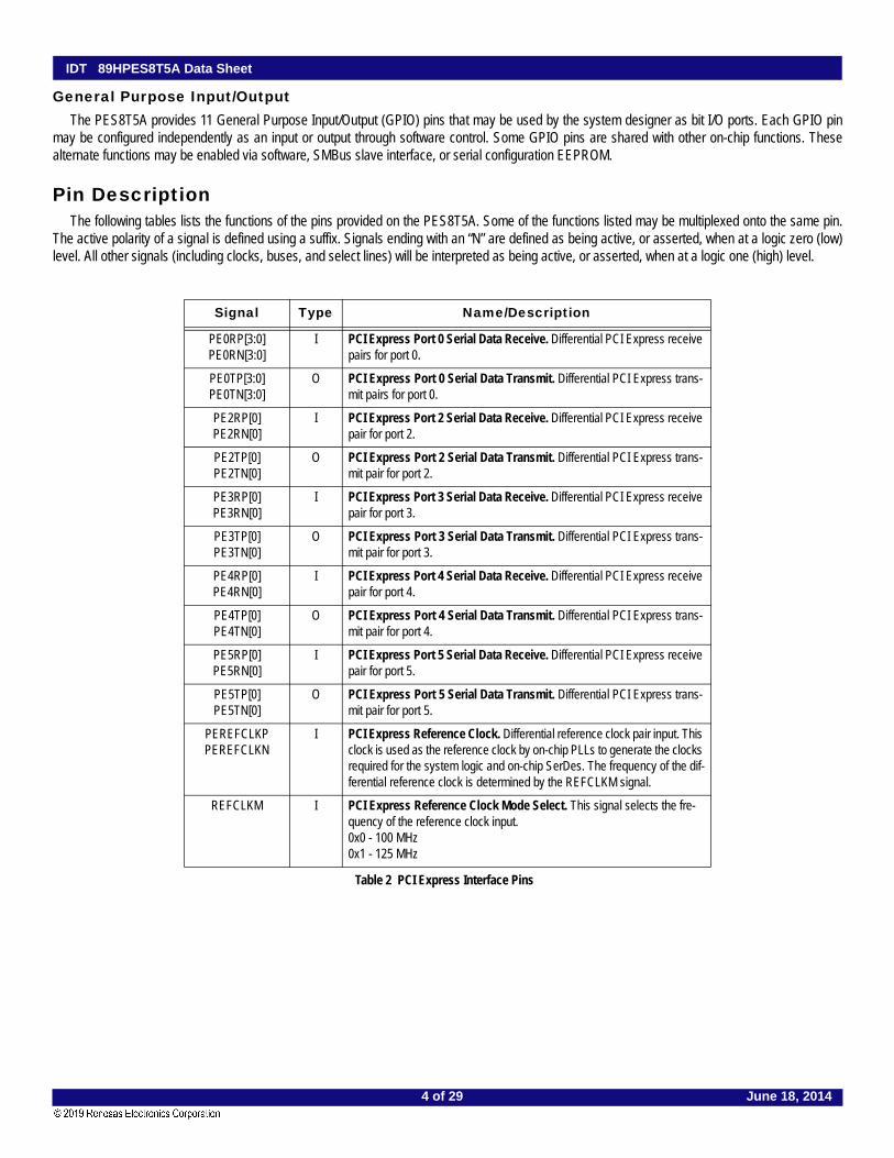
As shown in Figure 3, the master and slave SMBuses may be used in a unified or split configuration. In the unified configuration, shown in Figure3(a), the master and slave SMBuses are tied together and the PES8T5A acts both as a SMBus master as well as a SMBus slave on this bus. Thisrequires that the SMBus master or processor that has access to PES8T5A registers supports SMBus arbitration. In some systems, this SMBus masterinterface may be implemented using general purpose I/O pins on a processor or micro controller, and may not support SMBus arbitration. To supportthese systems, the PES8T5A may be configured to operate in a split configuration as shown in Figure 3(b).
In the split configuration, the master and slave SMBuses operate as two independent buses and thus multi-master arbitration is never required.The PES8T5A supports reading and writing of the serial EEPROM on the master SMBus via the slave SMBus, allowing in system programming of theserial EEPROM.
Figure 3 SMBus Interface Configuration Examples
Hot-Plug InterfaceThe PES8T5A supports PCI Express Hot-Plug on each downstream port. To reduce the number of pins required on the device, the PES8T5A
utilizes an external I/O expander, such as that used on PC motherboards, connected to the SMBus master interface. Following reset and configura-tion, whenever the state of a Hot-Plug output needs to be modified, the PES8T5A generates an SMBus transaction to the I/O expander with the newvalue of all of the outputs. Whenever a Hot-Plug input changes, the I/O expander generates an interrupt which is received on the IOEXPINTN input pin(alternate function of GPIO) of the PES8T5A. In response to an I/O expander interrupt, the PES8T5A generates an SMBus transaction to read thestate of all of the Hot-Plug inputs from the I/O expander.
BitSlave
SMBusAddress
MasterSMBus
Address
1 SSMBADDR[1] MSMBADDR[1]
2 SSMBADDR[2] MSMBADDR[2]
3 SSMBADDR[3] MSMBADDR[3]
4 0 MSMBADDR[4]
5 SSMBADDR[5] 1
6 1 0
7 1 1
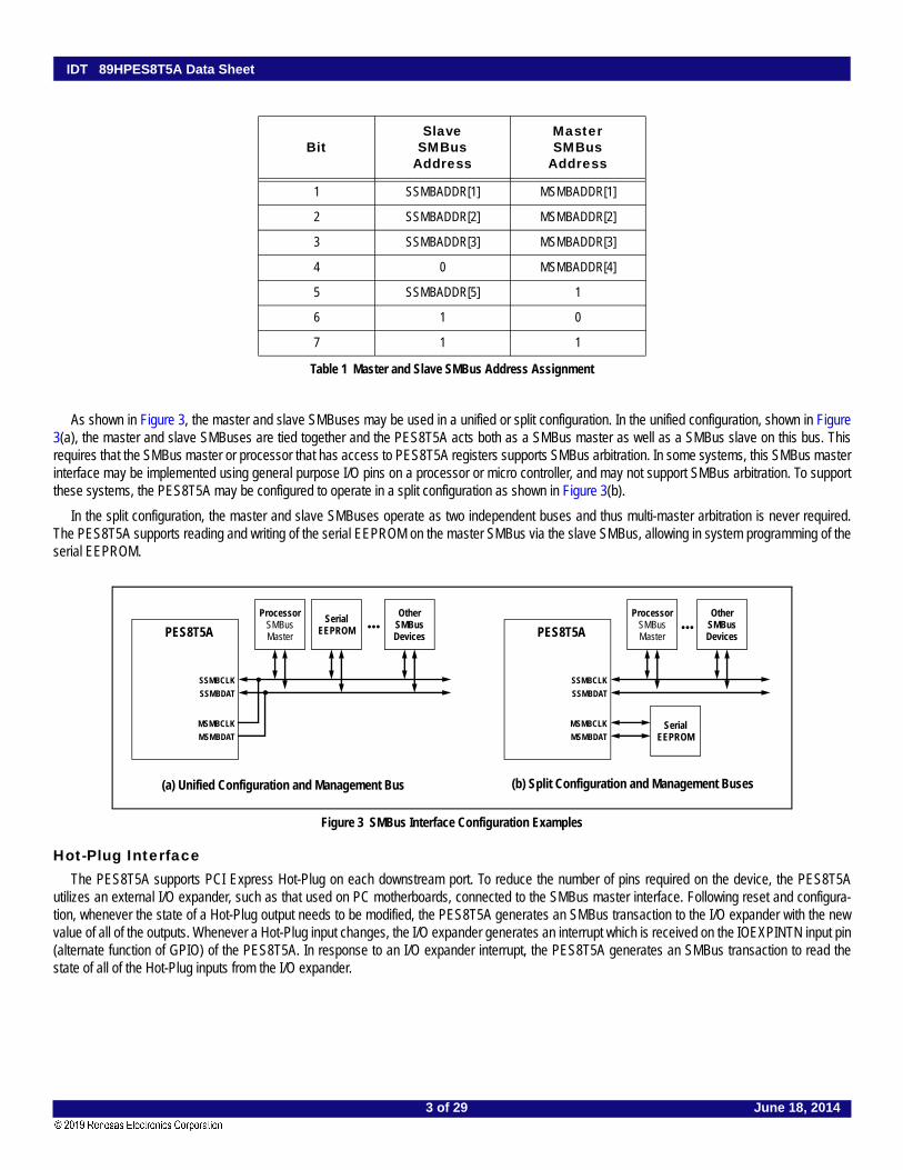
Table 1 Master and Slave SMBus Address Assignment
Processor
PES8T5A
SSMBCLK
SSMBDAT
MSMBCLK
MSMBDAT
SMBusMaster
OtherSMBusDevices
SerialEEPROM
Processor
PES8T5A
SSMBCLK
SSMBDAT
MSMBCLK
MSMBDAT
SMBusMaster
OtherSMBusDevices
SerialEEPROM
... ...
(a) Unified Configuration and Management Bus (b) Split Configuration and Management Buses
3 of 29 June 18, 2014
IDT 89HPES8T5A Data Sheet
General Purpose Input/OutputThe PES8T5A provides 11 General Purpose Input/Output (GPIO) pins that may be used by the system designer as bit I/O ports. Each GPIO pin
may be configured independently as an input or output through software control. Some GPIO pins are shared with other on-chip functions. Thesealternate functions may be enabled via software, SMBus slave interface, or serial configuration EEPROM.
Pin DescriptionThe following tables lists the functions of the pins provided on the PES8T5A. Some of the functions listed may be multiplexed onto the same pin.
The active polarity of a signal is defined using a suffix. Signals ending with an “N” are defined as being active, or asserted, when at a logic zero (low)level. All other signals (including clocks, buses, and select lines) will be interpreted as being active, or asserted, when at a logic one (high) level.
Signal Type Name/Description
PE0RP[3:0]PE0RN[3:0]
I PCI Express Port 0 Serial Data Receive. Differential PCI Express receive pairs for port 0.
PE0TP[3:0]PE0TN[3:0]
O PCI Express Port 0 Serial Data Transmit. Differential PCI Express trans-mit pairs for port 0.
PE2RP[0]PE2RN[0]
I PCI Express Port 2 Serial Data Receive. Differential PCI Express receive pair for port 2.
PE2TP[0]PE2TN[0]
O PCI Express Port 2 Serial Data Transmit. Differential PCI Express trans-mit pair for port 2.
PE3RP[0]PE3RN[0]
I PCI Express Port 3 Serial Data Receive. Differential PCI Express receive pair for port 3.
PE3TP[0]PE3TN[0]
O PCI Express Port 3 Serial Data Transmit. Differential PCI Express trans-mit pair for port 3.
PE4RP[0]PE4RN[0]
I PCI Express Port 4 Serial Data Receive. Differential PCI Express receive pair for port 4.
PE4TP[0]PE4TN[0]
O PCI Express Port 4 Serial Data Transmit. Differential PCI Express trans-mit pair for port 4.
PE5RP[0]PE5RN[0]
I PCI Express Port 5 Serial Data Receive. Differential PCI Express receive pair for port 5.
PE5TP[0]PE5TN[0]
O PCI Express Port 5 Serial Data Transmit. Differential PCI Express trans-mit pair for port 5.
PEREFCLKPPEREFCLKN
I PCI Express Reference Clock. Differential reference clock pair input. This clock is used as the reference clock by on-chip PLLs to generate the clocks required for the system logic and on-chip SerDes. The frequency of the dif-ferential reference clock is determined by the REFCLKM signal.
REFCLKM I PCI Express Reference Clock Mode Select. This signal selects the fre-quency of the reference clock input.0x0 - 100 MHz0x1 - 125 MHz
Table 2 PCI Express Interface Pins
4 of 29 June 18, 2014
IDT 89HPES8T5A Data Sheet
Signal Type Name/Description
MSMBADDR[4:1] I Master SMBus Address. These pins determine the SMBus address of the serial EEPROM from which configuration information is loaded.
MSMBCLK I/O Master SMBus Clock. This bidirectional signal is used to synchronize transfers on the master SMBus.
MSMBDAT I/O Master SMBus Data. This bidirectional signal is used for data on the mas-ter SMBus.
SSMBADDR[5,3:1] I Slave SMBus Address. These pins determine the SMBus address to which the slave SMBus interface responds.
SSMBCLK I/O Slave SMBus Clock. This bidirectional signal is used to synchronize trans-fers on the slave SMBus.
SSMBDAT I/O Slave SMBus Data. This bidirectional signal is used for data on the slave SMBus.
Table 3 SMBus Interface Pins
Signal Type Name/Description
GPIO[0] I/O General Purpose I/O.This pin can be configured as a general purpose I/O pin.Alternate function pin name: P2RSTNAlternate function pin type: OutputAlternate function: Reset output for downstream port 2
GPIO[1] I/O General Purpose I/O.This pin can be configured as a general purpose I/O pin.Alternate function pin name: P4RSTNAlternate function pin type: OutputAlternate function: Reset output for downstream port 4
GPIO[2] I/O General Purpose I/O.This pin can be configured as a general purpose I/O pin.Alternate function pin name: IOEXPINTN0Alternate function pin type: InputAlternate function: I/O Expander interrupt 0 input
GPIO[3] I/O General Purpose I/O.This pin can be configured as a general purpose I/O pin.Alternate function pin name: IOEXPINTN1Alternate function pin type: InputAlternate function: I/O Expander interrupt 1 input
GPIO[4] I/O General Purpose I/O.This pin can be configured as a general purpose I/O pin.Alternate function pin name: IOEXPINTN2Alternate function pin type: InputAlternate function: I/O Expander interrupt 2 input
GPIO[5] I/O General Purpose I/O.This pin can be configured as a general purpose I/O pin.
GPIO[6] I/O General Purpose I/O.This pin can be configured as a general purpose I/O pin.
Table 4 General Purpose I/O Pins (Part 1 of 2)
5 of 29 June 18, 2014
IDT 89HPES8T5A Data Sheet
GPIO[7] I/O General Purpose I/O.This pin can be configured as a general purpose I/O pin.Alternate function pin name: GPENAlternate function pin type: OutputAlternate function: General Purpose Event (GPE) output
GPIO[8] I/O General Purpose I/O.This pin can be configured as a general purpose I/O pin.
GPIO[9] I/O General Purpose I/O.This pin can be configured as a general purpose I/O pin.Alternate function pin name: P3RSTNAlternate function pin type: OutputAlternate function: Reset output for downstream port 3
GPIO[10] I/O General Purpose I/O.This pin can be configured as a general purpose I/O pin.Alternate function pin name: P5RSTNAlternate function pin type: OutputAlternate function: Reset output for downstream port 5
Signal Type Name/Description
APWRDISN I Auxiliary Power Disable Input. When this pin is active, it disables the device from using auxiliary power supply.
CCLKDS I Common Clock Downstream. The assertion of this pin indicates that all downstream ports are using the same clock source as that provided to downstream devices.This bit is used as the initial value of the Slot Clock Configuration bit in all of the Link Status Registers for downstream ports. The value may be override by modifying the SCLK bit in the downstream port’s PCIELSTS register.
CCLKUS I Common Clock Upstream. The assertion of this pin indicates that the upstream port is using the same clock source as the upstream device. This bit is used as the initial value of the Slot Clock Configuration bit in the Link Status Register for the upstream port. The value may be overridden by modifying the SCLK bit in the PA_PCIELSTS register.
MSMBSMODE I Master SMBus Slow Mode. The assertion of this pin indicates that the master SMBus should operate at 100 KHz instead of 400 kHz. This value may not be overridden.
PERSTN I Fundamental Reset. Assertion of this signal resets all logic inside the PES8T5A and initiates a PCI Express fundamental reset.
Table 5 System Pins (Part 1 of 2)
Signal Type Name/Description
Table 4 General Purpose I/O Pins (Part 2 of 2)
6 of 29 June 18, 2014

IDT 89HPES8T5A Data Sheet
RSTHALT I Reset Halt. When this signal is asserted during a PCI Express fundamental reset, the PES8T5A executes the reset procedure and remains in a reset state with the Master and Slave SMBuses active. This allows software to read and write registers internal to the device before normal device opera-tion begins. The device exits the reset state when the RSTHALT bit is cleared in the PA_SWCTL register by an SMBus master.
SWMODE[2:0] I Switch Mode. These configuration pins determine the PES8T5A switch operating mode.0x0 - Normal switch mode 0x1 - Normal switch mode with Serial EEPROM initialization0x2 - through 0xF Reserved
WAKEN I/O Wake Input/Output. The WAKEN signal is an input or output. The WAKEN signal input/output selection can be made through the WAKEDIR bit setting in the WAKEUPCNTL register.
Signal Type Name/Description
JTAG_TCK I JTAG Clock. This is an input test clock used to clock the shifting of data into or out of the boundary scan logic or JTAG Controller. JTAG_TCK is independent of the system clock with a nominal 50% duty cycle.
JTAG_TDI I JTAG Data Input. This is the serial data input to the boundary scan logic or JTAG Controller.
JTAG_TDO O JTAG Data Output. This is the serial data shifted out from the boundary scan logic or JTAG Controller. When no data is being shifted out, this signal is tri-stated.
JTAG_TMS I JTAG Mode. The value on this signal controls the test mode select of the boundary scan logic or JTAG Controller.
JTAG_TRST_N I JTAG Reset. This active low signal asynchronously resets the boundary scan logic and JTAG TAP Controller. An external pull-up on the board is recommended to meet the JTAG specification in cases where the tester can access this signal. However, for systems running in functional mode, one of the following should occur:1) actively drive this signal low with control logic2) statically drive this signal low with an external pull-down on the board
Table 6 Test Pins
Signal Type Name/Description
VDDCORE I Core VDD. Power supply for core logic.
VDDIO I I/O VDD. LVTTL I/O buffer power supply.
VDDPE I PCI Express Digital Power. PCI Express digital power used by the digital power of the SerDes.
VDDAPE I PCI Express Analog Power. PCI Express analog power used by the PLL and bias generator.
VTTPE I PCI Express Termination Power.
VSS I Ground.
Table 7 Power and Ground Pins
Signal Type Name/Description
Table 5 System Pins (Part 2 of 2)
7 of 29 June 18, 2014
IDT 89HPES8T5A Data Sheet
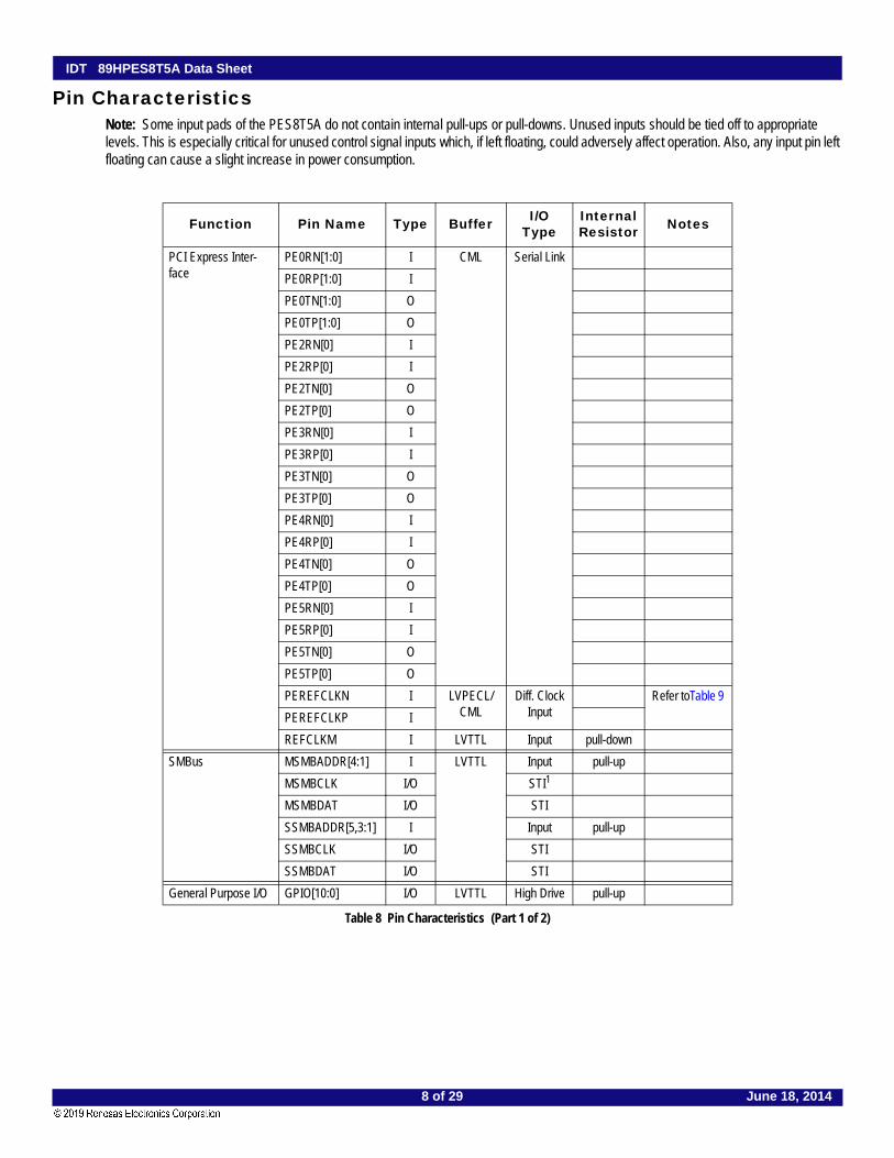
Pin CharacteristicsNote: Some input pads of the PES8T5A do not contain internal pull-ups or pull-downs. Unused inputs should be tied off to appropriate levels. This is especially critical for unused control signal inputs which, if left floating, could adversely affect operation. Also, any input pin left floating can cause a slight increase in power consumption.
Function Pin Name Type Buffer I/O Type
Internal Resistor Notes
PCI Express Inter-face
PE0RN[1:0] I CML Serial Link
PE0RP[1:0] I
PE0TN[1:0] O
PE0TP[1:0] O
PE2RN[0] I
PE2RP[0] I
PE2TN[0] O
PE2TP[0] O
PE3RN[0] I
PE3RP[0] I
PE3TN[0] O
PE3TP[0] O
PE4RN[0] I
PE4RP[0] I
PE4TN[0] O
PE4TP[0] O
PE5RN[0] I
PE5RP[0] I
PE5TN[0] O
PE5TP[0] O
PEREFCLKN I LVPECL/CML
Diff. Clock Input
Refer toTable 9
PEREFCLKP I
REFCLKM I LVTTL Input pull-down
SMBus MSMBADDR[4:1] I LVTTL Input pull-up
MSMBCLK I/O STI1
MSMBDAT I/O STI
SSMBADDR[5,3:1] I Input pull-up
SSMBCLK I/O STI
SSMBDAT I/O STI
General Purpose I/O GPIO[10:0] I/O LVTTL High Drive pull-up
Table 8 Pin Characteristics (Part 1 of 2)
8 of 29 June 18, 2014

IDT 89HPES8T5A Data Sheet
System Pins APWRDISN I LVTTL Input pull-down
CCLKDS I pull-up
CCLKUS I pull-up
MSMBSMODE I pull-down
PERSTN I pull-up
RSTHALT I pull-down
SWMODE[2:0] I pull-down
WAKEN I/O open-drain
EJTAG / JTAG JTAG_TCK I LVTTL STI pull-up
JTAG_TDI I STI pull-up
JTAG_TDO O
JTAG_TMS I STI pull-up
JTAG_TRST_N I STI pull-up
1. Schmitt Trigger Input (STI).
Function Pin Name Type Buffer I/O Type
Internal Resistor Notes
Table 8 Pin Characteristics (Part 2 of 2)
9 of 29 June 18, 2014

IDT 89HPES8T5A Data Sheet
Logic Diagram — PES8T5A
Figure 4 PES8T5A Logic Diagram
PEREFCLKPPEREFCLKN
JTAG_TCK
GPIO[10:0]11
VDDCOREVDDI/OVDDPEVDDAPE
MSMBADDR[4:1]MSMBCLKMSMBDAT
4
SSMBADDR[5,3:1]SSMBCLKSSMBDAT
4
CCLKUSRSTHALT
JTAG_TDIJTAG_TDOJTAG_TMSJTAG_TRST_N
VSS
SWMODE[2:0]3
CCLKDS
PERSTN
REFCLKM
MSMBSMODE
VTTPE
PE0RP[0]PE0RN[0]
PE0RP[3]PE0RN[3]
PE0TP[0]PE0TN[0]
PE0TP[3]PE0TN[3]
...
...PE2RP[0]PE2RN[0]
PE2TP[0]PE2TN[0]
PE3RN[0]
PE3TP[0]PE3TN[0]
PE4RP[0]PE4RN[0]
PE4TP[0]PE4TN[0]
PE5RP[0]PE5RN[0]
PE5TP[0]PE5TN[0]
PES8T5A
PE3RP[0]
WAKEN
Reference Clocks
Serdes Input Port 0
Serdes Input Port 2
Serdes Input Port 3
Serdes Input Port 4
Serdes Input Port 5
MasterSMBusInterface
SlaveSMBusInterface
System Pins
Serdes Output Port 2
Serdes Output Port 3
Serdes Output Port 4
Serdes Output Port 5
General Purpose
Power/Ground
APWRDISN
Serdes Output Port 1
I/O
10 of 29 June 18, 2014

IDT 89HPES8T5A Data Sheet
System Clock ParametersValues based on systems running at recommended supply voltages and operating temperatures, as shown in Tables 13 and 14.
AC Timing Characteristics
Parameter Description Min Typical Max Unit
PEREFCLK
RefclkFREQ Input reference clock frequency range 100 1251
1. The input clock frequency will be either 100 or 125 MHz depending on signal REFCLKM.
MHz
RefclkDC2
2. ClkIn must be AC coupled. Use 0.01 — 0.1 µF ceramic capacitors.
Duty cycle of input clock 40 50 60 %
TR, TF Rise/Fall time of input clocks 0.2*RCUI RCUI3
3. RCUI (Reference Clock Unit Interval) refers to the reference clock period.
VSW Differential input voltage swing4
4. AC coupling required.
0.6 1.6 V
Tjitter Input clock jitter (cycle-to-cycle) 125 ps
Table 9 Input Clock Requirements
Parameter Description Min1 Typical1 Max1 Units
PCIe Transmit
UI Unit Interval 399.88 400 400.12 ps
TTX-EYE Minimum Tx Eye Width 0.7 .9 UI
TTX-EYE-MEDIAN-to-
MAX-JITTER
Maximum time between the jitter median and maximum deviation from the median
0.15 UI
TTX-RISE, TTX-FALL D+ / D- Tx output rise/fall time 50 90 ps
TTX- IDLE-MIN Minimum time in idle 50 UI
TTX-IDLE-SET-TO-
IDLE
Maximum time to transition to a valid Idle after sending an Idle ordered set
20 UI
TTX-IDLE-TO-DIFF-
DATA
Maximum time to transition from valid idle to diff data 20 UI
TTX-SKEW Transmitter data skew between any 2 lanes 500 1300 ps
TBTEn Time from asserting Beacon TxEn to beacon being trans-mitted on the lane
30 80 ns
PCIe Receive
UI Unit Interval 399.88 400 400.12 ps
TRX-EYE (with jitter) Minimum Receiver Eye Width (jitter tolerance) 0.4 UI
Table 10 PCIe AC Timing Characteristics (Part 1 of 2)
11 of 29 June 18, 2014

IDT 89HPES8T5A Data Sheet
Figure 5 GPIO AC Timing Waveform
TRX-EYE-MEDIUM TO
MAX JITTER
Max time between jitter median & max deviation 0.3 UI
TRX-IDLE-DET-DIFF-
ENTER TIME
Unexpected Idle Enter Detect Threshold Integration Time 10 ms
TRX-SKEW Lane to lane input skew 20 ns
1. Minimum, Typical, and Maximum values meet the requirements under PCI Specification 1.1
Signal Symbol Reference Edge Min Max Unit
Timing Diagram
Reference
GPIO
GPIO[10:0]1
1. GPIO signals must meet the setup and hold times if they are synchronous or the minimum pulse width ifthey are asynchronous.
Tpw_13b2
2. The values for this symbol were determined by calculation, not by testing.
None 50 — ns See Figure 5.
Table 11 GPIO AC Timing Characteristics
Parameter Description Min1 Typical1 Max1 Units
Table 10 PCIe AC Timing Characteristics (Part 2 of 2)
Tdo_13aTdo_13a
Tpw_13b
EXTCLK
GPIO (synchronous output)
GPIO (asynchronous input)
12 of 29 June 18, 2014
IDT 89HPES8T5A Data Sheet
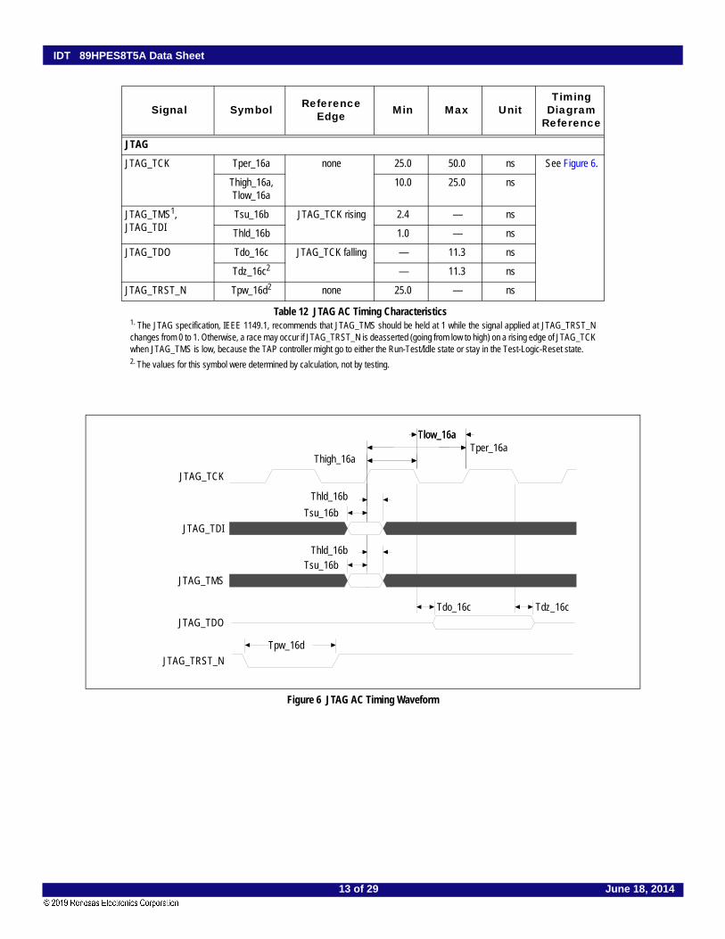
Figure 6 JTAG AC Timing Waveform
Signal Symbol Reference Edge Min Max Unit
Timing Diagram
Reference
JTAG
JTAG_TCK Tper_16a none 25.0 50.0 ns See Figure 6.
Thigh_16a,Tlow_16a
10.0 25.0 ns
JTAG_TMS1, JTAG_TDI
1. The JTAG specification, IEEE 1149.1, recommends that JTAG_TMS should be held at 1 while the signal applied at JTAG_TRST_Nchanges from 0 to 1. Otherwise, a race may occur if JTAG_TRST_N is deasserted (going from low to high) on a rising edge of JTAG_TCKwhen JTAG_TMS is low, because the TAP controller might go to either the Run-Test/Idle state or stay in the Test-Logic-Reset state.
Tsu_16b JTAG_TCK rising 2.4 — ns
Thld_16b 1.0 — ns
JTAG_TDO Tdo_16c JTAG_TCK falling — 11.3 ns
Tdz_16c2
2. The values for this symbol were determined by calculation, not by testing.
— 11.3 ns
JTAG_TRST_N Tpw_16d2 none 25.0 — ns
Table 12 JTAG AC Timing Characteristics
Tpw_16d
Tdz_16cTdo_16c
Thld_16bTsu_16b
Thld_16b
Tsu_16b
Tlow_16aTlow_16aTper_16a
Thigh_16a
JTAG_TCK
JTAG_TDI
JTAG_TMS
JTAG_TDO
JTAG_TRST_N
13 of 29 June 18, 2014
IDT 89HPES8T5A Data Sheet
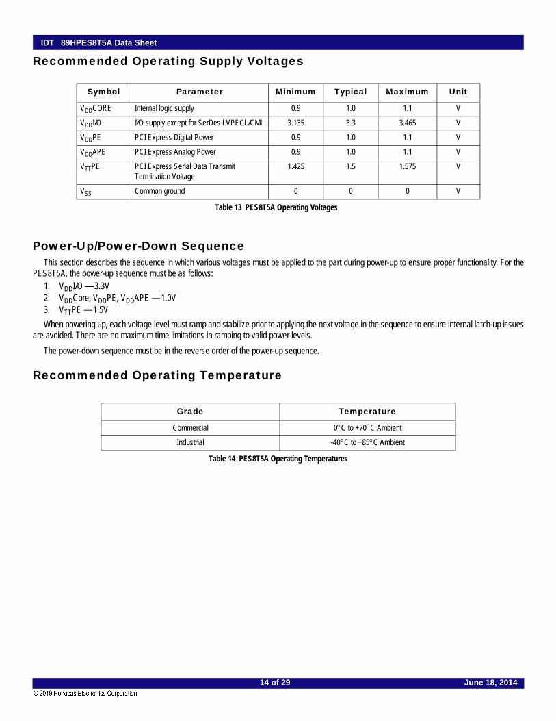
Recommended Operating Supply Voltages
Power-Up/Power-Down SequenceThis section describes the sequence in which various voltages must be applied to the part during power-up to ensure proper functionality. For the
PES8T5A, the power-up sequence must be as follows: 1. VDDI/O — 3.3V 2. VDDCore, VDDPE, VDDAPE — 1.0V 3. VTTPE — 1.5V
When powering up, each voltage level must ramp and stabilize prior to applying the next voltage in the sequence to ensure internal latch-up issuesare avoided. There are no maximum time limitations in ramping to valid power levels.
The power-down sequence must be in the reverse order of the power-up sequence.
Recommended Operating Temperature
Symbol Parameter Minimum Typical Maximum Unit
VDDCORE Internal logic supply 0.9 1.0 1.1 V
VDDI/O I/O supply except for SerDes LVPECL/CML 3.135 3.3 3.465 V
VDDPE PCI Express Digital Power 0.9 1.0 1.1 V
VDDAPE PCI Express Analog Power 0.9 1.0 1.1 V
VTTPE PCI Express Serial Data TransmitTermination Voltage
1.425 1.5 1.575 V
VSS Common ground 0 0 0 V
Table 13 PES8T5A Operating Voltages
Grade Temperature
Commercial 0C to +70C Ambient
Industrial -40C to +85C Ambient
Table 14 PES8T5A Operating Temperatures
14 of 29 June 18, 2014
IDT 89HPES8T5A Data Sheet
Power ConsumptionTypical power is measured under the following conditions: 25°C Ambient, 35% total link usage on all ports, typical voltages defined in Table 13.
Maximum power is measured under the following conditions: 70°C Ambient, 85% total link usage on all ports, maximum voltages defined in Table 13.
All power measurements assume that the part is mounted on a 10 layer printed circuit board with 0 LFM airflow.
Thermal ConsiderationsThis section describes thermal considerations for the PES8T5A (15mm2 BCG196 package). The data in Table 16 below contains information that
is relevant to the thermal performance of the PES8T5A switch.
Number of Connected
Lanes
Core Supply PCIe Digital Supply
PCIe Analog Supply
PCIe Termin-ation Supply I/O Supply Total
Typ1.0V
Max1.1V
Typ1.0V
Max1.1V
Typ1.0V
Max1.1V
Typ1.5V
Max1.575V
Typ3.3V
Max3.465V
TypPower
MaxPower
4/1/1/1/1 mA 308 495 327 440 130 187 161 222 3 3.3
Watts 0.31 0.54 0.33 0.48 0.13 0.21 0.24 0.35 0.01 0.01 1.02 1.60
Table 15 PES8T5A Power Consumption
Symbol Parameter Value Units Conditions
TJ(max) Junction Temperature 125 oC Maximum
TA(max) Ambient Temperature 70 oC Maximum for commercial-rated products
TA(max) Ambient Temperature 85 oC Maximum for industrial-rated products
JA(effective) Effective Thermal Resistance, Junction-to-Ambient
33.3 oC/W Zero air flow
29 oC/W 1 m/S air flow
26.6 oC/W 2 m/S air flow
JB Thermal Resistance, Junction-to-Board 18.7 oC/W
JC Thermal Resistance, Junction-to-Case 9.8 oC/W
P Power Dissipation of the Device 1.60 Watts Maximum
Table 16 Thermal Specifications for PES8T5A, 15x15mm BCG196 Package
15 of 29 June 18, 2014
IDT 89HPES8T5A Data Sheet
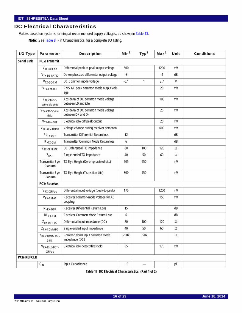
DC Electrical CharacteristicsValues based on systems running at recommended supply voltages, as shown in Table 13.
Note: See Table 8, Pin Characteristics, for a complete I/O listing.
I/O Type Parameter Description Min1 Typ1 Max1 Unit Conditions
Serial Link PCIe Transmit
VTX-DIFFp-p Differential peak-to-peak output voltage 800 1200 mV
VTX-DE-RATIO De-emphasized differential output voltage -3 -4 dB
VTX-DC-CM DC Common mode voltage -0.1 1 3.7 V
VTX-CM-ACP RMS AC peak common mode output volt-age
20 mV
VTX-CM-DC-
active-idle-delta
Abs delta of DC common mode voltage between L0 and idle
100 mV
VTX-CM-DC-line-
delta
Abs delta of DC common mode voltage between D+ and D-
25 mV
VTX-Idle-DiffP Electrical idle diff peak output 20 mV
VTX-RCV-Detect Voltage change during receiver detection 600 mV
RLTX-DIFF Transmitter Differential Return loss 12 dB
RLTX-CM Transmitter Common Mode Return loss 6 dB
ZTX-DEFF-DC DC Differential TX impedance 80 100 120
ZOSE Single ended TX Impedance 40 50 60
Transmitter Eye Diagram
TX Eye Height (De-emphasized bits) 505 650 mV
Transmitter Eye Diagram
TX Eye Height (Transition bits) 800 950 mV
PCIe Receive
VRX-DIFFp-p Differential input voltage (peak-to-peak) 175 1200 mV
VRX-CM-AC Receiver common-mode voltage for AC coupling
150 mV
RLRX-DIFF Receiver Differential Return Loss 15 dB
RLRX-CM Receiver Common Mode Return Loss 6 dB
ZRX-DIFF-DC Differential input impedance (DC) 80 100 120
ZRX-COMM-DC Single-ended input impedance 40 50 60
ZRX-COMM-HIGH-
Z-DC
Powered down input common mode impedance (DC)
200k 350k
VRX-IDLE-DET-
DIFFp-p
Electrical idle detect threshold 65 175 mV
PCIe REFCLK
CIN Input Capacitance 1.5 — pF
Table 17 DC Electrical Characteristics (Part 1 of 2)
16 of 29 June 18, 2014

IDT 89HPES8T5A Data Sheet
Other I/Os
LOW Drive Output
IOL — 2.5 — mA VOL = 0.4v
IOH — -5.5 — mA VOH = 1.5V
High Drive Output
IOL — 12.0 — mA VOL = 0.4v
IOH — -20.0 — mA VOH = 1.5V
Schmitt Trig-ger Input (STI)
VIL -0.3 — 0.8 V —
VIH 2.0 — VDDIO + 0.5
V —
Input VIL -0.3 — 0.8 V —
VIH 2.0 — VDDIO + 0.5
V —
Capacitance CIN — — 8.5 pF —
Leakage Inputs — — + 10 A VDDI/O (max)
I/OLEAK W/O Pull-ups/downs
— — + 10 A VDDI/O (max)
I/OLEAK WITHPull-ups/downs
— — + 80 A VDDI/O (max)
1. Minimum, Typical, and Maximum values meet the requirements under PCI Specification 1.1.
I/O Type Parameter Description Min1 Typ1 Max1 Unit Conditions
Table 17 DC Electrical Characteristics (Part 2 of 2)
17 of 29 June 18, 2014

IDT 89HPES8T5A Data Sheet
Package Pinout — 196-BGA Signal Pinout for PES8T5AThe following table lists the pin numbers and signal names for the PES8T5A device.
Pin Function Alt Pin Function Alt Pin Function Alt Pin Function Alt
A1 VSS C7 VDDAPE E13 VDDCORE H5 VSS
A2 PE0RP03 C8 VDDAPE E14 VSS H6 VDDCORE
A3 VSS C9 VTTPE F1 MSMBDAT H7 VDDCORE
A4 PE0TN03 C10 CCLKDS F2 SSMBADDR_2 H8 VSS
A5 PE0TP02 C11 VSS F3 SSMBADDR_5 H9 VSS
A6 VSS C12 VDDIO F4 VDDIO H10 VDDCORE
A7 PE0RN02 C13 VSS F5 VSS H11 VDDCORE
A8 PE0RN01 C14 SWMODE_0 F6 VDDCORE H12 GPIO_05
A9 VSS D1 SSMBCLK F7 VDDCORE H13 GPIO_03 1
A10 PE0TP01 D2 SSMBDAT F8 VSS H14 GPIO_02
A11 PE0TN00 D3 VSS F9 VDDCORE J1 JTAG_TDO
A12 VSS D4 VDDIO F10 VDDCORE J2 JTAG_TRST_N
A13 PE0RP00 D5 VDDCORE F11 VDDIO J3 JTAG_TMS
A14 VSS D6 VDDCORE F12 GPIO_00 1 J4 VDDCORE
B1 VSS D7 VDDPE F13 PERSTN J5 VSS
B2 PE0RN03 D8 VDDPE F14 VSS J6 VDDCORE
B3 VSS D9 VDDCORE G1 MSMBADDR_4 J7 VSS
B4 PE0TP03 D10 VDDIO G2 MSMBCLK J8 VDDCORE
B5 PE0TN02 D11 VDDCORE G3 VDDIO J9 VDDCORE
B6 VSS D12 VSS G4 VSS J10 VSS
B7 PE0RP02 D13 SWMODE_2 G5 VDDCORE J11 VDDIO
B8 PE0RP01 D14 SWMODE_1 G6 VSS J12 VDDIO
B9 VSS E1 SSMBADDR_1 G7 VSS J13 GPIO_06
B10 PE0TN01 E2 SSMBADDR_3 G8 VDDCORE J14 GPIO_04 1
B11 PE0TP00 E3 VDDIO G9 VSS K1 JTAG_TDI
B12 VSS E4 VDDCORE G10 VSS K2 VDDIO
B13 PE0RN00 E5 VSS G11 VSS K3 VDDAPE
B14 VSS E6 VSS G12 VDDIO K4 VSS
C1 WAKEN E7 VSS G13 GPIO_01 1 K5 VDDCORE
C2 APWRDISN E8 VSS G14 RSTHALT K6 VSS
C3 CCLKUS E9 VSS H1 MSMBADDR_1 K7 VSS
C4 VSS E10 VDDCORE H2 MSMBADDR_2 K8 VSS
C5 VSS E11 VSS H3 MSMBADDR_3 K9 VSS
C6 VTTPE E12 VDDIO H4 VDDCORE K10 VSS
Table 18 PES8T5A 196-pin Signal Pin-Out (Part 1 of 2)
18 of 29 June 18, 2014

IDT 89HPES8T5A Data Sheet
Alternate Signal Functions
K11 VDDCORE L12 VSS M13 MSMBSMODE N14 PE5RN00
K12 VSS L13 GPIO_10 1 M14 VSS P1 PEREFCLKP
K13 GPIO_08 L14 GPIO_09 1 N1 PEREFCLKN P2 VSS
K14 GPIO_07 1 M1 VSS N2 VSS P3 PE2RP00
L1 JTAG_TCK M2 VDDCORE N3 PE2RN00 P4 VSS
L2 VSS M3 VDDCORE N4 VSS P5 PE2TN00
L3 VSS M4 VSS N5 PE2TP00 P6 PE3TP00
L4 VDDIO M5 VDDIO N6 PE3TN00 P7 VSS
L5 VDDCORE M6 VTTPE N7 VSS P8 PE3RP00
L6 VDDCORE M7 VDDAPE N8 PE3RN00 P9 PE4RN00
L7 VDDPE M8 VDDAPE N9 PE4RP00 P10 VSS
L8 VDDPE M9 VTTPE N10 VSS P11 PE4TP00
L9 VDDCORE M10 VDDIO N11 PE4TN00 P12 PE5TN00
L10 VDDCORE M11 VDDIO N12 PE5TP00 P13 VSS
L11 VSS M12 REFCLKM N13 VSS P14 PE5RP00
Pin GPIO Alternate
F12 GPIO_00 P2RSTN
G13 GPIO_01 P4RSTN
H14 GPIO_02 IOEXPINTN0
H13 GPIO_03 IOEXPINTN1
J14 GPIO_04 IOEXPINTN2
K14 GPIO_07 GPEN
L14 GPIO_09 P3RSTN
L13 GPIO_10 P5RSTN
Table 19 PES8T5A Alternate Signal Functions
Pin Function Alt Pin Function Alt Pin Function Alt Pin Function Alt
Table 18 PES8T5A 196-pin Signal Pin-Out (Part 2 of 2)
19 of 29 June 18, 2014
IDT 89HPES8T5A Data Sheet
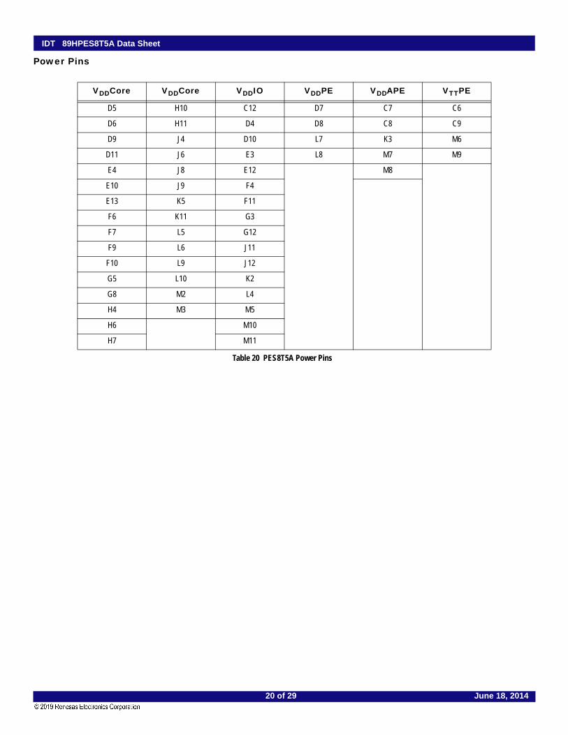
Power Pins
VDDCore VDDCore VDDIO VDDPE VDDAPE VTTPE
D5 H10 C12 D7 C7 C6
D6 H11 D4 D8 C8 C9
D9 J4 D10 L7 K3 M6
D11 J6 E3 L8 M7 M9
E4 J8 E12 M8
E10 J9 F4
E13 K5 F11
F6 K11 G3
F7 L5 G12
F9 L6 J11
F10 L9 J12
G5 L10 K2
G8 M2 L4
H4 M3 M5
H6 M10
H7 M11
Table 20 PES8T5A Power Pins
20 of 29 June 18, 2014

IDT 89HPES8T5A Data Sheet
Ground Pins
Vss Vss Vss Vss
A1 D3 G10 L3
A3 D12 G11 L11
A6 E5 H5 L12
A9 E6 H8 M1
A12 E7 H9 M4
A14 E8 J5 M14
B1 E9 J7 N2
B3 E11 J10 N4
B6 E14 K4 N7
B9 F5 K6 N10
B12 F8 K7 N13
B14 F14 K8 P2
C4 G4 K9 P4
C5 G6 K10 P7
C11 G7 K12 P10
C13 G9 L2 P13
Table 21 PES8T5A Ground Pins
21 of 29 June 18, 2014
IDT 89HPES8T5A Data Sheet
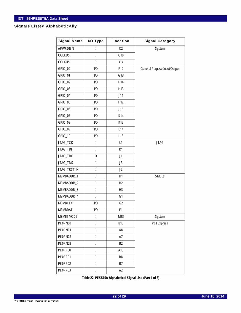
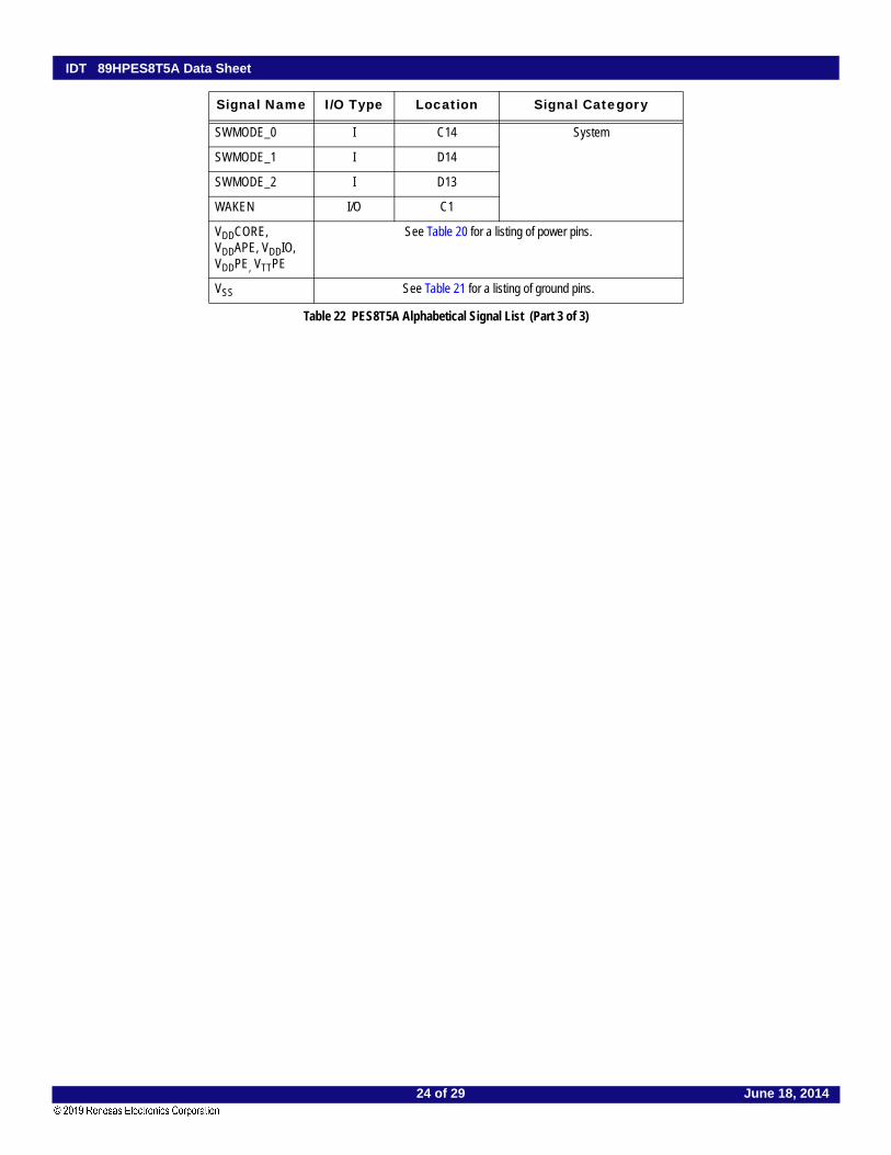
Signals Listed Alphabetically
Signal Name I/O Type Location Signal Category
APWRDISN I C2 System
CCLKDS I C10
CCLKUS I C3
GPIO_00 I/O F12 General Purpose Input/Output
GPIO_01 I/O G13
GPIO_02 I/O H14
GPIO_03 I/O H13
GPIO_04 I/O J14
GPIO_05 I/O H12
GPIO_06 I/O J13
GPIO_07 I/O K14
GPIO_08 I/O K13
GPIO_09 I/O L14
GPIO_10 I/O L13
JTAG_TCK I L1 JTAG
JTAG_TDI I K1
JTAG_TDO O J1
JTAG_TMS I J3
JTAG_TRST_N I J2
MSMBADDR_1 I H1 SMBus
MSMBADDR_2 I H2
MSMBADDR_3 I H3
MSMBADDR_4 I G1
MSMBCLK I/O G2
MSMBDAT I/O F1
MSMBSMODE I M13 System
PE0RN00 I B13 PCI Express
PE0RN01 I A8
PE0RN02 I A7
PE0RN03 I B2
PE0RP00 I A13
PE0RP01 I B8
PE0RP02 I B7
PE0RP03 I A2
Table 22 PES8T5A Alphabetical Signal List (Part 1 of 3)
22 of 29 June 18, 2014
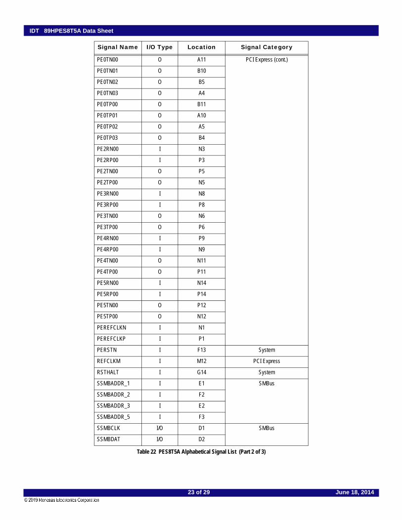
IDT 89HPES8T5A Data Sheet
PE0TN00 O A11 PCI Express (cont.)
PE0TN01 O B10
PE0TN02 O B5
PE0TN03 O A4
PE0TP00 O B11
PE0TP01 O A10
PE0TP02 O A5
PE0TP03 O B4
PE2RN00 I N3
PE2RP00 I P3
PE2TN00 O P5
PE2TP00 O N5
PE3RN00 I N8
PE3RP00 I P8
PE3TN00 O N6
PE3TP00 O P6
PE4RN00 I P9
PE4RP00 I N9
PE4TN00 O N11
PE4TP00 O P11
PE5RN00 I N14
PE5RP00 I P14
PE5TN00 O P12
PE5TP00 O N12
PEREFCLKN I N1
PEREFCLKP I P1
PERSTN I F13 System
REFCLKM I M12 PCI Express
RSTHALT I G14 System
SSMBADDR_1 I E1 SMBus
SSMBADDR_2 I F2
SSMBADDR_3 I E2
SSMBADDR_5 I F3
SSMBCLK I/O D1 SMBus
SSMBDAT I/O D2
Signal Name I/O Type Location Signal Category
Table 22 PES8T5A Alphabetical Signal List (Part 2 of 3)
23 of 29 June 18, 2014
IDT 89HPES8T5A Data Sheet
SWMODE_0 I C14 System
SWMODE_1 I D14
SWMODE_2 I D13
WAKEN I/O C1
VDDCORE, VDDAPE, VDDIO, VDDPE, VTTPE
See Table 20 for a listing of power pins.
VSS See Table 21 for a listing of ground pins.
Signal Name I/O Type Location Signal Category
Table 22 PES8T5A Alphabetical Signal List (Part 3 of 3)
24 of 29 June 18, 2014
IDT 89HPES8T5A Data Sheet
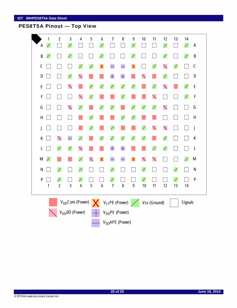
PES8T5A Pinout — Top View
1 2 3 4 5 6 7 8 9 10 11 12 13 14
Vss (Ground)VDDCore (Power)
VDDI/O (Power)
VTTPE (Power)
VDDPE (Power)
VDDAPE (Power)
Signals
A
B
C
D
E
F
G
H
J
K
L
M
N
P
x
A
B
C
D
E
F
G
H
J
K
L
M
N
P1 2 3 4 5 6 7 8 9 10 11 12 13 14
XX
X X
25 of 29 June 18, 2014

IDT 89HPES8T5A Data Sheet
PES8T5A Package Drawing — 196-Pin BC196/BCG196
26 of 29 June 18, 2014

IDT 89HPES8T5A Data Sheet
PES8T5A Package Drawing — Page Two
27 of 29 June 18, 2014

IDT 89HPES8T5A Data Sheet
Revision HistoryMarch 31, 2008: Publication of final data sheet.
August 6, 2008: Added industrial temperature information to Tables 14 and 16 and to Ordering Information section.
May 7, 2009: Revised labels in Table 15, Power Consumption, for greater clarification.
June 18, 2014: Changed the height dimension for the side view in PES8T5A Package Drawing — 196-Pin BC196/BCG196 to match the package’scharacteristics.
28 of 29 June 18, 2014
IDT 89HPES8T5A Data Sheet
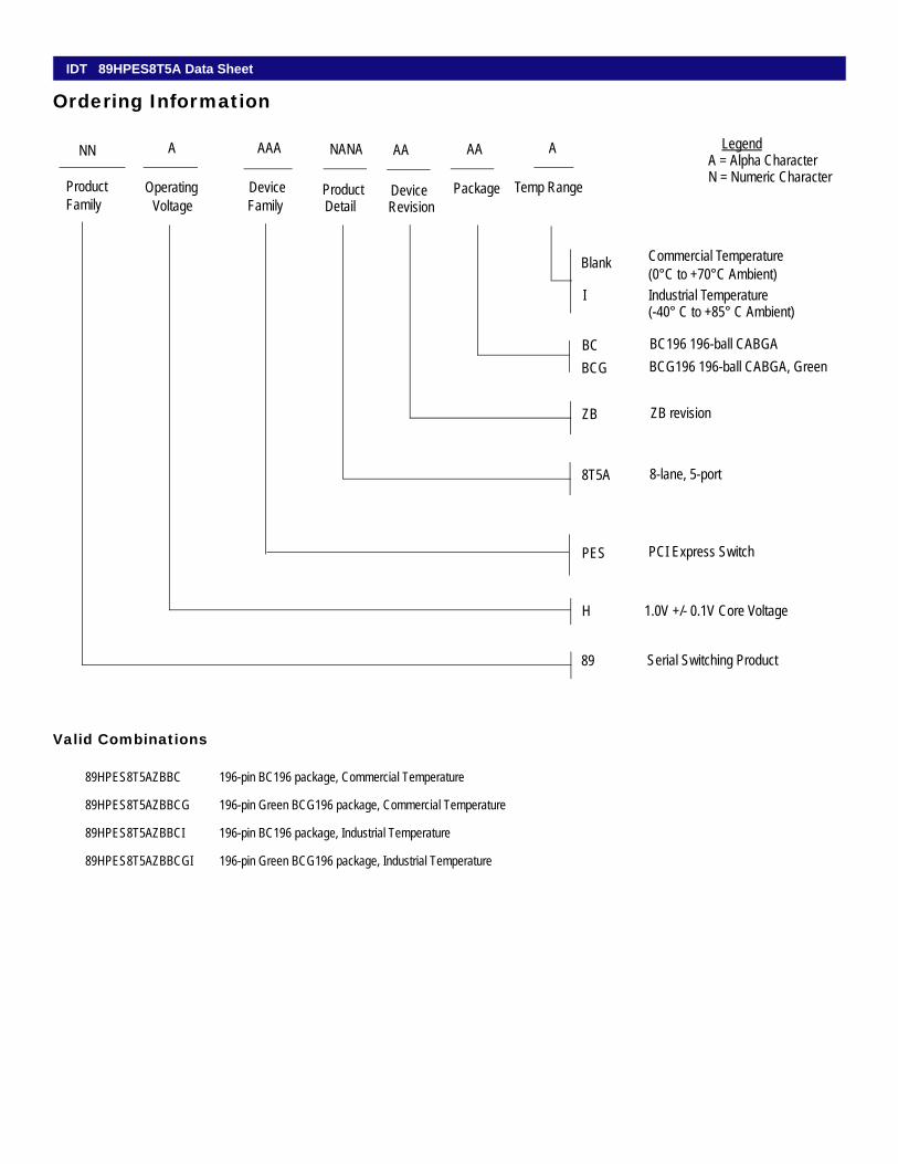
Ordering Information
Valid Combinations
89HPES8T5AZBBC 196-pin BC196 package, Commercial Temperature
89HPES8T5AZBBCG 196-pin Green BCG196 package, Commercial Temperature
89HPES8T5AZBBCI 196-pin BC196 package, Industrial Temperature
89HPES8T5AZBBCGI 196-pin Green BCG196 package, Industrial Temperature
NN A AAA NANA AA A
Operating Voltage
DeviceFamily
Product Package Temp Range
H
Blank Commercial Temperature(0°C to +70°C Ambient)
ProductFamily
89 Serial Switching Product
BC196 196-ball CABGA BC
8T5A 8-lane, 5-port
1.0V +/- 0.1V Core Voltage
Detail
PCI Express SwitchPES
LegendA = Alpha CharacterN = Numeric Character
BCG196 196-ball CABGA, Green BCG
AA
DeviceRevision
ZB ZB revision
I Industrial Temperature (-40° C to +85° C Ambient)
29 of 29 June 18, 2014
CORPORATE HEADQUARTERS6024 Silver Creek Valley RoadSan Jose, CA 95138
for SALES:800-345-7015 or 408-284-8200fax: 408-284-2775www.idt.com
for Tech Support:email: [email protected]: 408-284-8208
®
Corporate HeadquartersTOYOSU FORESIA, 3-2-24 Toyosu,Koto-ku, Tokyo 135-0061, Japanwww.renesas.com
Contact InformationFor further information on a product, technology, the most up-to-date version of a document, or your nearest sales office, please visit:www.renesas.com/contact/
TrademarksRenesas and the Renesas logo are trademarks of Renesas Electronics Corporation. All trademarks and registered trademarks are the property of their respective owners.
IMPORTANT NOTICE AND DISCLAIMER
RENESAS ELECTRONICS CORPORATION AND ITS SUBSIDIARIES (“RENESAS”) PROVIDES TECHNICAL SPECIFICATIONS AND RELIABILITY DATA (INCLUDING DATASHEETS), DESIGN RESOURCES (INCLUDING REFERENCE DESIGNS), APPLICATION OR OTHER DESIGN ADVICE, WEB TOOLS, SAFETY INFORMATION, AND OTHER RESOURCES “AS IS” AND WITH ALL FAULTS, AND DISCLAIMS ALL WARRANTIES, EXPRESS OR IMPLIED, INCLUDING, WITHOUT LIMITATION, ANY IMPLIED WARRANTIES OF MERCHANTABILITY, FITNESS FOR A PARTICULAR PURPOSE, OR NON-INFRINGEMENT OF THIRD PARTY INTELLECTUAL PROPERTY RIGHTS.
These resources are intended for developers skilled in the art designing with Renesas products. You are solely responsible for (1) selecting the appropriate products for your application, (2) designing, validating, and testing your application, and (3) ensuring your application meets applicable standards, and any other safety, security, or other requirements. These resources are subject to change without notice. Renesas grants you permission to use these resources only for development of an application that uses Renesas products. Other reproduction or use of these resources is strictly prohibited. No license is granted to any other Renesas intellectual property or to any third party intellectual property. Renesas disclaims responsibility for, and you will fully indemnify Renesas and its representatives against, any claims, damages, costs, losses, or liabilities arising out of your use of these resources. Renesas' products are provided only subject to Renesas' Terms and Conditions of Sale or other applicable terms agreed to in writing. No use of any Renesas resources expands or otherwise alters any applicable warranties or warranty disclaimers for these products.
(Rev.1.0 Mar 2020)
© 2020 Renesas Electronics Corporation. All rights reserved.