Embed Size (px)
Citation preview
DS50PCI402
www.ti.com SNLS320H –APRIL 2010–REVISED MARCH 2013
DS50PCI402 2.5 Gbps / 5.0 Gbps 4 Lane PCI Express Repeater withEqualization and De-Emphasis
Check for Samples: DS50PCI402
1FEATURES DESCRIPTIONThe DS50PCI402 is a low power, 4 lane bidirectional
2• Input and Output signal conditioningbuffer/equalizer designed specifically for PCI Expressincreases PCIe reach in backplanes andGen1 and Gen2 applications. The device performscablesboth receive equalization and transmit de-emphasis,
• 0.09 UI of residual deterministic jitter at 5Gbps allowing maximum flexibility of physical placementafter 42” of FR4 (with Input EQ) within a system. The receiver is capable of opening
an input eye that is completely closed due to inter-• 0.11 UI of residual deterministic jitter at 5Gbpssymbol interference (ISI) induced by the interconnectafter 7m of PCIe Cable (with Input EQ)medium.
• 0.09 UI of residual deterministic jitter at 5GbpsThe transmitter de-emphasis level can be set by thewith 28” of FR4 (with Output DE)user depending on the distance from the• 0.13 UI of residual deterministic jitter at 5GbpsDS50PCI402 to the PCI Express endpoint. Thewith 7m of PCIe Cable (with Output DE) DS50PCI402 contains PCI Express specific functions
• Adjustable Transmit VOD 800 to 1200mVp-p such as Transmit Idle, RX Detection, and Beaconsignal pass through.• Automatic and manual Receiver Detection and
input termination control circuitry The device provides automatic receive detection• Automatic power management on an circuitry which controls the input termination
impedance. By automatically reflecting the currentindividual lane basis via SMBusload impedance seen on the outputs back to the• Adjustable electrical idle detect threshold.corresponding inputs the DS50PCI402 becomes
• Data rate optimized 3-stage equalization to 27 completely transparent to both the PCIe root complexdB gain and endpoint. An internal rate detection circuit is
included to detect if an incoming data stream is at• Data rate optimized 6-level 0 to 12 dB transmitGen2 data rates, and adjusts the de-emphasis on it'sde-emphasisoutput accordingly. The signal conditioning provided• Flow-thru pinout in 10mmx5.5mm 54-pinby the device allows systems to upgrade from Gen1
leadless WQFN package data rates to Gen2 without reducing their physical• Single supply operation at 2.5V reach. This is true for FR4 applications such as
backplanes, as well as cable interconnect.• >6kV HBM ESD rating• -10 to 85°C operating temperature range
1
Please be aware that an important notice concerning availability, standard warranty, and use in critical applications ofTexas Instruments semiconductor products and disclaimers thereto appears at the end of this data sheet.
2All trademarks are the property of their respective owners.
PRODUCTION DATA information is current as of publication date. Copyright © 2010–2013, Texas Instruments IncorporatedProducts conform to specifications per the terms of the TexasInstruments standard warranty. Production processing does notnecessarily include testing of all parameters.

Ix_n+
Ix_n-
EQ
RATEDET
LIMITER
IDLE DET
OUTBUF
SMBus
VOD/ DeEMPHASIS CONTROL
VDD
SMBus
TX Idle Enable
SMBus
Auto / ManualRXDETECT
DEMA/B
EQA/B
Ox_n+
Ox_n-
TXIDLEx
PCI ExpressRoot
Complex or Bridge
PCI Express Endpoint
PCI Express InterconnectCable or Backplane
PCI402Slice 1 of 4
PCI402Slice 1 of 4
DS50PCI402
SNLS320H –APRIL 2010–REVISED MARCH 2013 www.ti.com
Typical Application
Block Diagram - Detail View Of Channel (1 of 8)
2 Submit Documentation Feedback Copyright © 2010–2013, Texas Instruments Incorporated
Product Folder Links: DS50PCI402

OB_0+
OB_0-
OB_1+
RX
DE
TB
RX
DE
TA
SD
_TH
1
2
3
4
2625
DAP = GND
OB_1-
OB_2+
OB_2-
5
6
7
242120 23
IA_3-
8
IA_0+
IA_0-
VDD
IA_1+
9
10
11
12
IA_1-
EQ
A0
IA_2+
IA_2-
13
18
14
15
IA_3+
16
17
OA_1+
OA_1-
EQ
A1
OA_2+
36
34
35
OA_2-
OA_3+
OA_3-
33
31
32
TX
IDLE
A
TX
IDLE
B
IB_3+
IB_3-
VDD
41
40
39R
AT
E
OA_0+
OA_0-
37
38
IB_0+
IB_0-
IB_1+
IB_1-
IB_2-
IB_2+
44
42
43
VD
D
DE
MA
1/S
CL
50 48 4749D
EM
A0/
SD
A
EN
SM
B
4651
OB_3+
OB_3-
SMBUS AND CONTROL
DE
MB
1/A
D0
DE
MB
0/A
D1
30
29
28
EN
RX
DE
T
52
EQ
B1/
AD
2
EQ
B0/
AD
3
19 22
PR
SN
T
27
45
5354
VDD
VDD
DS50PCI402
www.ti.com SNLS320H –APRIL 2010–REVISED MARCH 2013
Pin Diagram
The center DAP on the package bottom is the device GND connection. This pad must be connected to GND throughmultiple (minimum of 8) vias to ensure optimal electrical and thermal performance.
DS50PCI402 Pin Diagram 54 lead
Copyright © 2010–2013, Texas Instruments Incorporated Submit Documentation Feedback 3
Product Folder Links: DS50PCI402

DS50PCI402
SNLS320H –APRIL 2010–REVISED MARCH 2013 www.ti.com
Table 1. Pin Descriptions
Pin Name Pin Number I/O, Pin DescriptionType (1) (2) (3) (4)
Differential High Speed I/O's
IA_0+, IA_0- , 10, 11 I, CML Inverting and non-inverting CML differential inputs to the equalizer. AIA_1+, IA_1-, 12, 13 gated on-chip 50Ω termination resistor connects INA_0+ to VDD andIA_2+, IA_2-, 15, 16 INA_0- to VDD when enabled.IA_3+, IA_3- 17, 18
OA_0+, OA_0-, 35, 34 O,LPDS Inverting and non-inverting low power differential signal (LPDS) 50ΩOA_1+, OA_1-, 33, 32 driver outputs with de-emphasis. Compatible with AC coupled CMLOA_2+, OA_2-, 31, 30 inputs.OA_3+, OA_3- 29, 28
IB_0+, IB_0- , 45, 44 I, CML Inverting and non-inverting CML differential inputs to the equalizer. AIB_1+, IB_1-, 43, 42 gated on-chip 50Ω termination resistor connects INB_0+ to VDD andIB_2+, IB_2-, 40, 39 INB_0- to VDD when enabled.IB_3+, IB_3- 38, 37
OB_0+, OB_0-, 1, 2 O,LPDS Inverting and non-inverting low power differential signal (LPDS) 50ΩOB_1+, OB_1-, 3, 4 driver outputs with de-emphasis. Compatible with AC coupled CMLOB_2+, OB_2-, 5, 6 inputs.OB_3+, OB_3- 7, 8
Control Pins — Shared (LVCMOS)
ENSMB 48 I, LVCMOS System Management Bus (SMBus) enable pin.w/internal When pulled high provide access internal digital registers that are apulldown means of auxiliary control for such functions as equalization, de-
emphasis, VOD, rate, and idle detection threshold.When pulled low, access to the SMBus registers are disabled andSMBus function pins are used to control the Equalizer and De-Emphasis.Please refer to SYSTEM MANAGEMENT BUS (SMBUS) ANDCONFIGURATION REGISTERS and Electrical Characteristics — SerialManagement Bus Interface for detail information.
ENSMB = 1 (SMBUS MODE)
SCL 50 I, LVCMOS ENSMB = 1SMBUS clock input pin is enabled. External pull-up resistor maybeneeded. Refer to RTERM in the SMBus specification.
SDA 49 I, LVCMOS, ENSMB = 1O, Open Drain The SMBus bi-directional SDA pin is enabled. Data input or open drain
output. External pull-up resistor is required.Refer to RTERM in the SMBus specification.
AD0-AD3 54, 53, 47, 46 I, LVCMOS ENSMB = 1w/internal SMBus Slave Address Inputs. In SMBus mode, these pins are the userpulldown set SMBus slave address inputs. See section — SYSTEM
MANAGEMENT BUS (SMBUS) AND CONFIGURATION REGISTERSfor additional information.
ENSMB = 0 (NORMAL PIN MODE)
EQA0, EQA1 20, 19 I,FLOAT, EQA/B ,0/1 controls the level of equalization of the A/B sides as shown inEQB0, EQB1 46, 47 LVCMOS Table 2. The EQA/B pins are active only when ENSMB is de-asserted
(Low). Each of the 4 A/B channels have the same level unless controlledby the SMBus control registers. When ENSMB goes high the SMBusregisters provide independent control of each lane, and the EQB0/B1pins are converted to SMBUS AD2/AD3 inputs.
DEMA0, DEMA1 49, 50 I,FLOAT, DEMA/B ,0/1 controls the level of de-emphasis of the A/B sides asDEMB0, DEMB1 53, 54 LVCMOS shown in Table 5. The DEMA/B pins are only active when ENSMB is de-
asserted (Low). Each of the 4 A/B channels have the same level unlesscontrolled by the SMBus control registers. When ENSMB goes High theSMBus registers provide independent control of each lane and the DEMpins are converted to SMBUS AD0/AD1 and SCL/SDA inputs.
(1) FLOAT = 3rd input state, don't drive pin. Pin is internally biased to mid level with 50 kΩ pull-up/pull-down. If high Z output not available,drive input to VDD/2 to assert mid level state.
(2) Internal pulldown = Internal 30 kΩ pull-down resistor to GND is present on the input.(3) LVCMOS inputs without the “Float” conditions must be driven to a logic Low or High at all times or operation is not ensured.(4) Input edge rate for LVCMOS/FLOAT inputs must be faster than 50 ns from 10–90%.
4 Submit Documentation Feedback Copyright © 2010–2013, Texas Instruments Incorporated
Product Folder Links: DS50PCI402

DS50PCI402
www.ti.com SNLS320H –APRIL 2010–REVISED MARCH 2013
Table 1. Pin Descriptions (continued)
Pin Name Pin Number I/O, Pin DescriptionType (1) (2) (3) (4)
RATE 21 I,FLOAT, RATE control pin controls the pulse width of de-emphasis of the output.LVCMOS A Low forces Gen1 (2.5Gbps), High forces Gen 2 (5Gbps),
Open/Floating the rate is internally detected after each exit from idle andthe pulse width is set appropriately. When ENSMBUS= 1 this pin isdisabled and the RATE function is controlled internally by the SMBUSregisters. Refer to Table 5.
Control Pins — Both Modes (LVCMOS)
RXDETA,RXDETB 22,23 I, LVCMOS The RXDET pins in combination with the ENRXDET pin controls thew/internal receiver detect function. Depending on the input level, a 50Ω or >50KΩpulldown termination to the power rail is enabled. Refer to Table 7.
PRSNT 52 I, LVCMOS Cable Present Detect input. High when a cable is not present per PCIeCabling Spec. 1.0. Puts part into low power mode. When low (normaloperation) part is enabled.
ENRXDET 26 I, LVCMOS Enables pin control of receiver detect function. The default is automaticw/internal RXDET using the internal pulldown. Pin must be pulled high for manualpulldown RXDETA/B operation. Controls individual A and B sides. Refer to
Table 7.
TXIDLEA,TXIDLEB 24,25 I, FLOAT, Controls the electrical idle function on corresponding outputs whenLVCMOS enabled. H= electrical Idle, Float=autodetect (Idle on input passed to
output), L=Idle squelch disabled as shown in Table 6.
Analog
SD_TH 27 I, ANALOG Threshold select pin for electrical idle detect threshold. Float pin fordefault 130mV DIFF p-p, otherwise connect resistor from SD_TH to GNDto set threshold voltage as shown in Table 7.
Power
VDD 9, 14,36, 41, 51 Power Power supply pins CML/analog.
GND DAP Power Ground pad (DAP - die attach pad).
Copyright © 2010–2013, Texas Instruments Incorporated Submit Documentation Feedback 5
Product Folder Links: DS50PCI402

DS50PCI402
SNLS320H –APRIL 2010–REVISED MARCH 2013 www.ti.com
FUNCTIONAL DESCRIPTION
The DS50PCI402 is a low power media compensation 4 lane repeater optimized for PCI Express Gen 1 and Gen2 media including lossy FR-4 printed circuit board backplanes and balanced cables. The DS50PCI402 operatesin two modes: Pin Control Mode (ENSMB = 0) and SMBus Mode (ENSMB = 1).
Pin Control Mode:
When in pin mode (ENSMB = 0) , the repeater is configurable with external pins. Equalization and de-emphasiscan be selected via pin for each side independently. When de-emphasis is asserted VOD is automaticallyincreased per the De-Emphasis table below for improved performance over lossy media. The receiver detectpins RXDETA/B provide manual control for input termination (50Ω or >50KΩ). Rate optimization is also pincontrollable, with pin selections for 2.5Gbps, 5Gbps, and auto detect. The receiver electrical idle detect thresholdis also programmable via an optional external resistor on the SD_TH pin.
SMBUS Mode:
When in SMBus mode the equalization, de-emphasis, and termination disable features are all programmable ona individual lane basis, instead of grouped by sides as in the pin mode case. Upon assertion of ENSMB theRATE, EQx and DEMx functions revert to register control immediately. The EQx and DEMx pins are converted toAD0-AD3 SMBus address inputs. The other external control pins remain active unless their respective registersare written to and the appropriate override bit is set, in which case they are ignored until ENSMB is driven low.On powerup and when ENSMB is driven low all registers are reset to their default state. If PRSNT is assertedwhile ENSMB is high, the registers retain their current state.
Equalization settings accessible via the pin controls were chosen to meet the needs of most PCIe applications. Ifadditional fine tuning or adjustment is needed, additional equalization settings can be accessed via the SMBusregisters. Each input has a total of 24 possible equalization settings. The tables show a typical gain for each gainstage (GST[1:0]) and boost level (BST[2:0]) combination. When using SMBus mode, the Equalization and De-Emphasis levels are set using registers.
Table 2. Equalization Settings with GST=1 for Pins or SMBus Registers
EQ Setting EQ Gain (dB)EQ1 ( EQ0 (
Suggested UseGST[1 BST[2: 1.25 GHz 2.5 GHz1) 1)
:0] 0]
F F 00 000 0 0 Bypass - Default Setting
01 000 1.6 3.2
01 001 2.1 4.2
1 1 01 010 2.6 5.0 8" FR4 (6-mil trace) or < 1m (28 AWG) PCIe cable
01 011 3.2 5.9
01 100 4.0 7.3
01 101 4.9 7.9
01 110 5.4 8.5
01 111 5.6 9.0
(1) F=Float (don't drive pin, each float pin has an internal 50K Ohm resistor to VDD and GND), 1=High, 0=Low
Table 3. Equalization Settings with GST=2 for Pins or SMBus Registers
EQ Setting EQ Gain (dB)EQ1 ( EQ0 (
Suggested UseGST[1 BST[2: 1.25 GHz 2.5 GHz1) 1)
:0] 0]
0 0 10 000 3.8 7.6 14" FR4 (6-mil trace) or 1m (28 AWG) PCIe cable
10 001 5.1 9.9
F 0 10 010 6.4 11.6 20" FR4 (6-mil trace) or 5m (26 AWG) PCIe cable
10 011 7.6 13.5
10 100 9.5 16.1
F 1 10 101 11.3 17.5 40" FR4 (6-mil trace) or 9m (24 AWG) PCIe cable
(1) F=Float (don't drive pin, each float pin has an internal 50K Ohm resistor to VDD and GND), 1=High, 0=Low
6 Submit Documentation Feedback Copyright © 2010–2013, Texas Instruments Incorporated
Product Folder Links: DS50PCI402

DS50PCI402
www.ti.com SNLS320H –APRIL 2010–REVISED MARCH 2013
Table 3. Equalization Settings with GST=2 for Pins or SMBus Registers (continued)
EQ Setting EQ Gain (dB)EQ1 ( EQ0 (
Suggested UseGST[1 BST[2: 1.25 GHz 2.5 GHz1) 1)
:0] 0]
10 110 12.3 18.6
0 1 10 111 12.8 19.8 50" FR4 (6-mil trace) or 10m (24 AWG) PCIe cable
Table 4. Equalization Settings with GST=3 for Pins or SMBus Registers
EQ Setting EQ Gain (dB)EQ1 ( EQ0 (
Suggested UseGST[1 BST[2: 1.25 GHz 2.5 GHz1) 1)
:0] 0]
11 000 6.4 12.2
1 0 11 001 8.5 15.6 30" FR4 (6-mil trace) or 7m (24 AWG) PCIe cable
11 010 10.4 18.3
0 F 11 011 12.4 21.3 15m (24 AWG) PCIe cable
11 100 15.2 25.0
1 F 11 101 18.1 27.2 > 15m (24 AWG) PCIe cable
11 110 19.6 28.8
11 111 20.2 30.7
(1) F=Float (don't drive pin, each float pin has an internal 50K Ohm resistor to VDD and GND), 1=High, 0=Low
The De-Emphasis level must be set when in SMBus mode. See SMBus TRANSACTIONS section andTable 10 for specific De-Emphasis values.
Table 5. De-Emphasis Input Select Pins for A and B ports (3–Level Input)
RATE DEM1 DEM0 (1 Typical De- Typical DE Pulse Typical VOD Suggested Use(1) ) Emphasis Level Width
0/F 0 0 0dB 0ps 1000mV
0/F 0 1 -3.5dB 400ps 1000mV 8 inches FR4 (6-mil trace) or less than 1meter (28 AWG) PCIe cable
0/F 1 0 -6dB 400ps 1000mV
0/F 1 1 -6dB 400ps enhanced 1000mV 15 inches FR4 (6-mil trace)
0/F 0 F -9dB 400ps enhanced 1000mV
0/F 1 F -12dB 400ps enhanced 1000mV
0/F F 0 -9dB 400ps enhanced 1200mV 30 inches FR4 (6-mil trace)
0/F F 1 -12dB 400ps enhanced 1400mV 40 inches FR4 (6-mil trace)
0/F F F Reserved, don'tuse
1/F 0 0 0dB 0ps 1000mV
1/F 0 1 -3.5dB 200ps 1000mV
1/F 1 0 -6dB 200ps 1000mV
1/F 1 1 -6dB 200ps enhanced 1000mV 10 inches FR4 (6-mil trace)
1/F 0 F -9dB 200ps enhanced 1000mV
1/F 1 F -12dB 200ps enhanced 1000mV
1/F F 0 -9dB 200ps enhanced 1200mV 20 inches FR4 (6-mil trace)
1/F F 1 -12dB 200ps enhanced 1400mV 30 inches FR4 (6-mil trace)
1/F F F Reserved, don'tuse
(1) F=Float (don't drive pin - (each float pin has an internal 50K Ohm resistor to VDD and GND). Enhanced DE Pulse width providesadditional de-emphasis on second bit. VOD = Voltage Output Differential amplitude. When RATE is floated (F=Auto Rate DetectionActive) DE Level and Pulse Width settings follow detected RATE. RATE=0 is 2.5GBps, RATE=1 is 5 GBps
Copyright © 2010–2013, Texas Instruments Incorporated Submit Documentation Feedback 7
Product Folder Links: DS50PCI402

0
50
100
150
200
250
0 10k 20k 30k 40k 50k 60k 70k 80k
SD_TH RESISTOR VALUE (:)
EL
EC
TR
ICA
L ID
LE
DE
TE
CT
TH
RE
SH
OL
D(D
IFF
mV
p-p
)
VDD = 2.5V TA = 25°C
DS50PCI402
SNLS320H –APRIL 2010–REVISED MARCH 2013 www.ti.com
Table 6. Idle Control (3–Level Input)
TXIDLEA/B Function
0 This state is for lossy media, dedicated Idle threshold detect circuit disabled,output follows input based on EQ settings. Idle state not ensured.
Float Float enables automatic idle detection. Idle on the input is passed to theoutput. This is the recommended default state. Output driven to Idle if diff input
signal less than value set by SD_TH pin.
1 Manual override, output forced to Idle. Diff inputs are ignored.
Table 7. Receiver Electrical Idle Detect Threshold Adjust (Analog input - Connect Resistor to GND orFloat)
SD_TH resistor value (Ω) (connect from pin to GND) (1) Typical Receiver Electrical Idle Detect Threshold (DIFF p-p)
Float (no resistor required) 130mV (default condition)
0 225mV
80K 20mV
(1) SD_TH resistor value can be set from 0 through 80K Ohms to achieve desired idle detect threshold, see Figure 1. 8K Ohm is approx130mV.
Figure 1. Typical Idle threshold vs SD_TH resistor value
Receiver Detection
The Rx detection process is a feature that can set the number of active channels on the DS50PCI402. Bysensing the presence of a valid PCIe load on the output, the channel can be automatically enabled for operation.This allows the DS50PCI402 to configure inself to the proper lane width, whether it is a 4-lane, 2-lane, or 1-lanePCIe link.
Automatic Rx Detection is enabled by a combination of PRSNT# and ENRXDET inputs. When these inputs areset low, Automatic Rx Detection is enabled, cycling of the PRSNT# pin will reset the Rx detection circuitry,initiating a new receiver detection sequence. Pulling the ENRXDET input to logic 1, allows for manual control ofthe input termination.
The table below summarizes control pin and receiver detect operation for the DS50PCI402.
8 Submit Documentation Feedback Copyright © 2010–2013, Texas Instruments Incorporated
Product Folder Links: DS50PCI402
DS50PCI402
www.ti.com SNLS320H –APRIL 2010–REVISED MARCH 2013
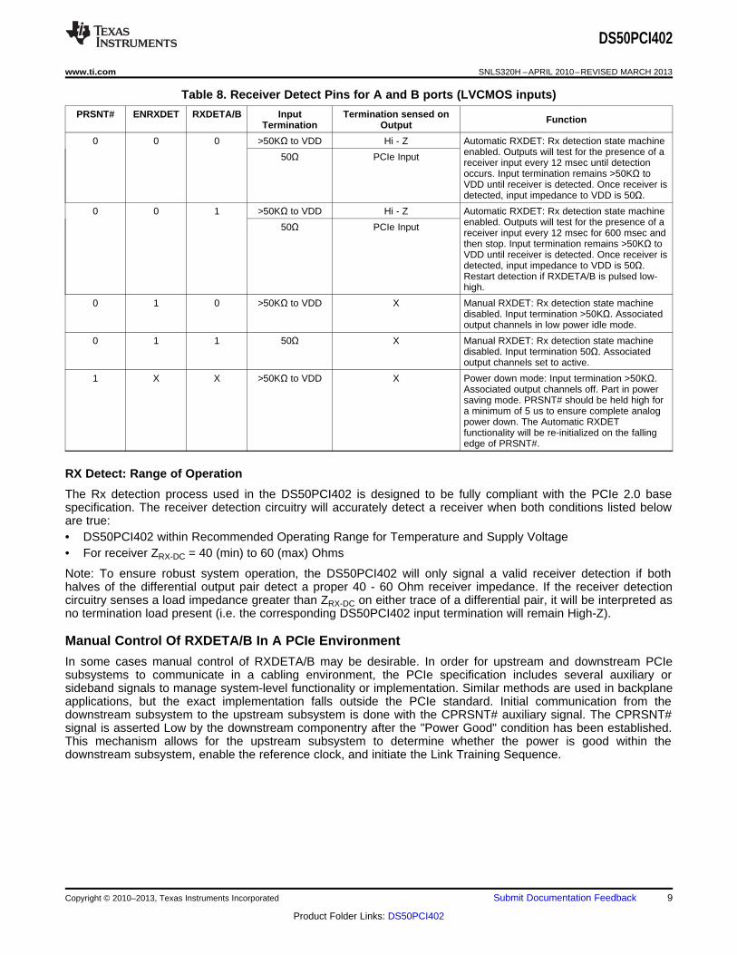
Table 8. Receiver Detect Pins for A and B ports (LVCMOS inputs)
PRSNT# ENRXDET RXDETA/B Input Termination sensed on FunctionTermination Output
0 0 0 >50KΩ to VDD Hi - Z Automatic RXDET: Rx detection state machineenabled. Outputs will test for the presence of a50Ω PCIe Inputreceiver input every 12 msec until detectionoccurs. Input termination remains >50KΩ toVDD until receiver is detected. Once receiver isdetected, input impedance to VDD is 50Ω.
0 0 1 >50KΩ to VDD Hi - Z Automatic RXDET: Rx detection state machineenabled. Outputs will test for the presence of a50Ω PCIe Inputreceiver input every 12 msec for 600 msec andthen stop. Input termination remains >50KΩ toVDD until receiver is detected. Once receiver isdetected, input impedance to VDD is 50Ω.Restart detection if RXDETA/B is pulsed low-high.
0 1 0 >50KΩ to VDD X Manual RXDET: Rx detection state machinedisabled. Input termination >50KΩ. Associatedoutput channels in low power idle mode.
0 1 1 50Ω X Manual RXDET: Rx detection state machinedisabled. Input termination 50Ω. Associatedoutput channels set to active.
1 X X >50KΩ to VDD X Power down mode: Input termination >50KΩ.Associated output channels off. Part in powersaving mode. PRSNT# should be held high fora minimum of 5 us to ensure complete analogpower down. The Automatic RXDETfunctionality will be re-initialized on the fallingedge of PRSNT#.
RX Detect: Range of Operation
The Rx detection process used in the DS50PCI402 is designed to be fully compliant with the PCIe 2.0 basespecification. The receiver detection circuitry will accurately detect a receiver when both conditions listed beloware true:• DS50PCI402 within Recommended Operating Range for Temperature and Supply Voltage• For receiver ZRX-DC = 40 (min) to 60 (max) Ohms
Note: To ensure robust system operation, the DS50PCI402 will only signal a valid receiver detection if bothhalves of the differential output pair detect a proper 40 - 60 Ohm receiver impedance. If the receiver detectioncircuitry senses a load impedance greater than ZRX-DC on either trace of a differential pair, it will be interpreted asno termination load present (i.e. the corresponding DS50PCI402 input termination will remain High-Z).
Manual Control Of RXDETA/B In A PCIe Environment
In some cases manual control of RXDETA/B may be desirable. In order for upstream and downstream PCIesubsystems to communicate in a cabling environment, the PCIe specification includes several auxiliary orsideband signals to manage system-level functionality or implementation. Similar methods are used in backplaneapplications, but the exact implementation falls outside the PCIe standard. Initial communication from thedownstream subsystem to the upstream subsystem is done with the CPRSNT# auxiliary signal. The CPRSNT#signal is asserted Low by the downstream componentry after the "Power Good" condition has been established.This mechanism allows for the upstream subsystem to determine whether the power is good within thedownstream subsystem, enable the reference clock, and initiate the Link Training Sequence.
Copyright © 2010–2013, Texas Instruments Incorporated Submit Documentation Feedback 9
Product Folder Links: DS50PCI402

CPRSNT#
CREFCLK
5 ms (min)
0V
RESET Removed and REFCLK Stable
0V
CPWRON
0V
CPERST#
CPRSNT# to RESET Removal
5 Ps (min)DS50PCI402 PRSNT#Min pulse width HIGH
DS50PCI402
SNLS320H –APRIL 2010–REVISED MARCH 2013 www.ti.com
Figure 2. Typical PCIe System Timing
The signals shown in the graphic could be easily replicated within the downstream subsystem and used toexternally control the common mode input termination impedance on the DS50PCI402. Often an onboardmicrocontroller will be used to handle events like power-up, power-down, power saving modes, and hot insertion.The microcontroller would use the same information to determine when to enable and disable the DS50PCI402input termination. In applications that require SMBus control, the microcontroller could also delay any responseto the upstream subsystem to allow sufficient time to correctly program the DS50PCI402 and other devices onthe board.
These devices have limited built-in ESD protection. The leads should be shorted together or the device placed in conductive foamduring storage or handling to prevent electrostatic damage to the MOS gates.
10 Submit Documentation Feedback Copyright © 2010–2013, Texas Instruments Incorporated
Product Folder Links: DS50PCI402

DS50PCI402
www.ti.com SNLS320H –APRIL 2010–REVISED MARCH 2013
Absolute Maximum Ratings (1) (2)
Supply Voltage (VDD) -0.5V to +3.0V
LVCMOS Input/Output Voltage -0.5V to +4.0V
CML Input Voltage -0.5V to (VDD+0.5V)
CML Input Current -30 to +30 mA
LPDS Output Voltage -0.5V to (VDD+0.5V)
Analog (SD_TH) (3) -0.5V to (VDD+0.5V)
Junction Temperature +125°C
Storage Temperature -40°C to +125°C
Lead Temperature Range
Maximum Package Power Dissipation at 25°C
NJY Package 4.21 W
Derate NJY Package 52.6mW/°C above +25°C
ESD Rating
HBM, STD - JESD22-A114C ≥6 kV
MM, STD - JESD22-A115-A ≥250 V
CDM, STD - JESD22-C101-C ≥1250 V
Thermal Resistance
θJC 11.5°C/W
θJA, No Airflow, 4 layer JEDEC 19.1°C/W
For soldering specifications: see product folder at
www.ti.com
http://www.ti.com/lit/SNOA549
(1) “Absolute Maximum Ratings” indicate limits beyond which damage to the device may occur, including inoperability and degradation ofdevice reliability and/or performance. Functional operation of the device and/or non-degradation at the Absolute Maximum Ratings orother conditions beyond those indicated in the Recommended Operating Conditions is not implied. The Recommended OperatingConditions indicate conditions at which the device is functional and the device should not be operated beyond such conditions. AbsoluteMaximum Numbers are specified for a junction temperature range of -40°C to +125°C. Models are validated to Maximum OperatingVoltages only.
(2) If Military/Aerospace specified devices are required, please contact the Texas Instruments Sales Office / Distributors foravailability and specifications.
(3) Measured at default SD_TH settings
Recommended Operating ConditionsMin Typ Max Units
Supply Voltage
VDD to GND 2.375 2.5 2.625 V
Ambient Temperature -10 25 +85 °C
SMBus (SDA, SCL) 3.6 V
Supply Noise Tolerance up to 50Mhz (1) 100 mV pp
(1) Allowed supply noise (mVP-P sine wave) under typical conditions.
Copyright © 2010–2013, Texas Instruments Incorporated Submit Documentation Feedback 11
Product Folder Links: DS50PCI402

DS50PCI402
SNLS320H –APRIL 2010–REVISED MARCH 2013 www.ti.com
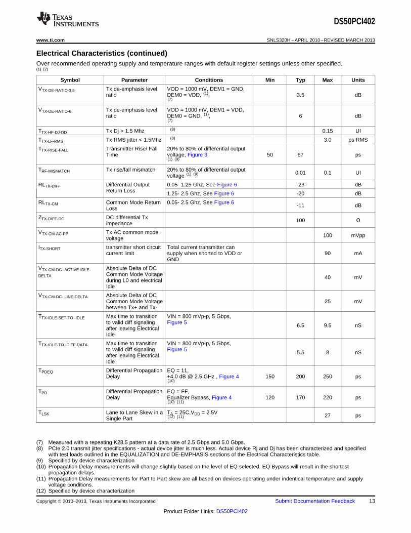
Electrical CharacteristicsOver recommended operating supply and temperature ranges with default register settings unless other specified.(1) (2)
Symbol Parameter Conditions Min Typ Max Units
POWER (3)
EQX=Float, DEX=0, VOD=1Vpp 800 1000 mW,PRSNT=0PD Power DissipationPRSNT=1, ENSMB=0 4 8 mW
LVCMOS / LVTTL DC SPECIFICATIONS
VIH High Level Input (4) 2 3.6 VVoltage
VIL Low Level Input (4) 0 0.8 VVoltage
VOH High Level Output SMBUS open drain VOH set by VVoltage pullup Resistor
VOL Low Level Output IOL = 4mA 0.4 VVoltage
IIH Input High Current VIN = 3.6V , LVCMOS -15 +15μAVIN = 3.6V , w/ -15 +120
FLOAT,PULLDOWN input
IIL Input Low Current VIN = 0V -15 +15μA
VIN = 0V, w/FLOAT input -80 +15
CML RECEIVER INPUTS (IN_n+, IN_n-)
RLRX-DIFF Rx package plus Si 0.05GHz – 1.25GHz (5) -21dBdifferential return loss 1.25GHz – 2.5GHz (5) -20
RLRX-CM Common mode Rx 0.05GHz - 2.5GHz (5)-11.5 dBreturn loss
ZRX-DC Rx DC common mode Tested at VDD=0 40 50 60 Ωimpedance
ZRX-DIFF-DC Rx DC differential Tested at VDD=0 85 100 115 Ωimpedance
VRX-DIFF-DC Differential Rx peak to Tested at DC, TXIDLEx=0 0.10 1.2 Vpeak voltage
ZRX-HIGH-IMP-DC -POS DC Input CM Vin = 0 to 200 mV,impedance for V>0 RXDETA/B = 0, 50 KΩ
ENSMB = 0, VDD=2.625
VRX-IDLE-DET-DIFF-PP Electrical Idle detect SD_TH = float, see Table 5, 40 175 mVP-Pthreshold (6)
LPDS OUTPUTS (OUT_n+, OUT_n-)
VTX-DIFF-PP Output Voltage Swing Differential measurement withOUT_n+ and OUT_n- terminated 800 1000 1200 mVP-Pby 50Ω to GND AC-Coupled,Figure 4, (3)
VOCM Output Common-Mode Single-ended measurement DC- VDD - 1.4 VVoltage Coupled with 50Ω termination, (1)
(1) Typical values represent most likely parametric norms at VDD = 2.5V, TA = 25°C., and at the Recommended Operation Conditions at thetime of product characterization and are not ensured.
(2) The Electrical Characteristics tables list ensured specifications under the listed Recommended Operating Conditions except asotherwise modified or specified by the Electrical Characteristics Conditions and/or Notes. Typical specifications are estimations only andare not ensured.
(3) Measured with DEM Select pins configured for 1000mV VOD, see De-emphasis table.(4) Input edge rate for LVCMOS/FLOAT inputs must be 50ns minimum from 10-90%.(5) Input Return Loss also uses the setup shown in Figure 6. The blocking / biasing circuit is replaced with a simple AC coupling capacitor
for each input to emulate a typical PCIe application.(6) Measured at package pins of receiver. Less than 40mV is IDLE, greater than 175mV is ACTIVE. SD_TH pin connected with resistor to
GND overrides this default setting.
12 Submit Documentation Feedback Copyright © 2010–2013, Texas Instruments Incorporated
Product Folder Links: DS50PCI402
DS50PCI402
www.ti.com SNLS320H –APRIL 2010–REVISED MARCH 2013
Electrical Characteristics (continued)Over recommended operating supply and temperature ranges with default register settings unless other specified.(1) (2)
Symbol Parameter Conditions Min Typ Max Units
VTX-DE-RATIO-3.5 Tx de-emphasis level VOD = 1000 mV, DEM1 = GND,ratio DEM0 = VDD, (1), 3.5 dB
(7)
VTX-DE-RATIO-6 Tx de-emphasis level VOD = 1000 mV, DEM1 = VDD,ratio DEM0 = GND, (1), 6 dB
(7)
TTX-HF-DJ-DD Tx Dj > 1.5 Mhz (8) 0.15 UI
TTX-LF-RMS Tx RMS jitter < 1.5Mhz (8) 3.0 ps RMS
TTX-RISE-FALL Transmitter Rise/ Fall 20% to 80% of differential outputTime voltage, Figure 3 50 67 ps
(1) (9)
TRF-MISMATCH Tx rise/fall mismatch 20% to 80% of differential output 0.01 0.1 UIvoltage (1) (9)
RLTX-DIFF Differential Output 0.05- 1.25 Ghz, See Figure 6 -23 dBReturn Loss 1.25- 2.5 Ghz, See Figure 6 -20 dB
RLTX-CM Common Mode Return 0.05- 2.5 Ghz, See Figure 6 -11 dBLoss
ZTX-DIFF-DC DC differential Tx 100 Ωimpedance
VTX-CM-AC-PP Tx AC common mode 100 mVppvoltage
ITX-SHORT transmitter short circuit Total current transmitter cancurrent limit supply when shorted to VDD or 90 mA
GND
VTX-CM-DC- ACTIVE-IDLE- Absolute Delta of DCDELTA Common Mode Voltage 40 mVduring L0 and electrical
Idle
VTX-CM-DC- LINE-DELTA Absolute Delta of DCCommon Mode Voltage 25 mVbetween Tx+ and Tx-
TTX-IDLE-SET-TO -IDLE Max time to transition VIN = 800 mVp-p, 5 Gbps,to valid diff signaling Figure 5 6.5 9.5 nSafter leaving ElectricalIdle
TTX-IDLE-TO -DIFF-DATA Max time to transition VIN = 800 mVp-p, 5 Gbps,to valid diff signaling Figure 5 5.5 8 nSafter leaving ElectricalIdle
TPDEQ Differential Propagation EQ = 11,Delay +4.0 dB @ 2.5 GHz , Figure 4 150 200 250 ps
(10)
TPD Differential Propagation EQ = FF,Delay Equalizer Bypass, Figure 4 120 170 220 ps
(10) (11)
TLSK Lane to Lane Skew in a TA = 25C,VDD = 2.5V 27 psSingle Part (12) (11)
(7) Measured with a repeating K28.5 pattern at a data rate of 2.5 Gbps and 5.0 Gbps.(8) PCIe 2.0 transmit jitter specifications - actual device jitter is much less. Actual device Rj and Dj has been characterized and specified
with test loads outlined in the EQUALIZATION and DE-EMPHASIS sections of the Electrical Characteristics table.(9) Specified by device characterization(10) Propagation Delay measurements will change slightly based on the level of EQ selected. EQ Bypass will result in the shortest
propagation delays.(11) Propagation Delay measurements for Part to Part skew are all based on devices operating under indentical temperature and supply
voltage conditions.(12) Specified by device characterization
Copyright © 2010–2013, Texas Instruments Incorporated Submit Documentation Feedback 13
Product Folder Links: DS50PCI402

DS50PCI402
SNLS320H –APRIL 2010–REVISED MARCH 2013 www.ti.com
Electrical Characteristics (continued)Over recommended operating supply and temperature ranges with default register settings unless other specified.(1) (2)
Symbol Parameter Conditions Min Typ Max Units
TPPSK Part to Part TA = 25C,VDD = 2.5VPropagation Delay 35 psSkew
EQUALIZATION
DJE1 Residual Deterministic 42” of 5 mil stripline FR4,Jitter at 5 Gbps EQ1,0=F,1; K28.5 pattern, 0.02 0.09 UIP-PDEMx=0, Tx Launch Amplitude 1.0
Vp-p, SD_TH=F. (13) (14)
Residual Deterministic 42” of 5 mil stripline FR4,Jitter at 2.5 Gbps EQ1,0=F,1; K28.5 pattern,DJE2 0.02 0.04 UIP-PDEMx=0, Tx Launch Amplitude 1.0
Vp-p, SD_TH=F. (13) (14)
DJE3 Residual Deterministic 7 meters of 24 AWG PCIe cable,Jitter at 5 Gbps EQ1,0=1,0; K28.5 pattern, 0.02 0.11 UIP-PDEMx=0, Tx Launch Amplitude 1.0
Vp-p, SD_TH=F. (13) (14)
Residual Deterministic 7 meters of 24 AWG PCIe cable,Jitter at 2.5 Gbps EQ1,0=1,0; K28.5 pattern,DJE4 0.03 0.07 UIP-PDEMx=0, Tx Launch Amplitude 1.0
Vp-p, SD_TH=F. (13) (14)
RJ Random Jitter Tx Launch Amplitude 1.0 Vp-p,SD_TH=F, Repeating 1100b <0.5 psrms(D24.3) pattern. (13)
DE-EMPHASIS
Residual Deterministic 28” of 5 mil stripline FR4,Jitter at 5 Gbps EQ1,0=F,F; K28.5 pattern,
DJD1 DEM1,0=F,1; Tx Launch 0.02 0.09 UIP-PAmplitude 1.0 Vp-p, SD_TH=F. (13)
(14)
Residual Deterministic 28” of 5 mil microstrip FR4,Jitter at 2.5 Gbps EQ1,0=F,F; K28.5 pattern,
DJD2 DEM1,0=F,0; Tx Launch 0.03 0.05 UIP-PAmplitude 1.0 Vp-p, SD_TH=F. (15)
(16)
Residual Deterministic 7 meters of 24 AWG PCIe cable,Jitter at 5 Gbps EQ1,0=F,F; K28.5 pattern,
DJD3 DEM1,0=F,1; Tx Launch 0.03 0.13 UIP-PAmplitude 1.0 Vp-p, SD_TH=F. (15)
(16)
Residual Deterministic 7 meters of 24 AWG PCIe cable,Jitter at 2.5 Gbps EQ1,0=F,F; K28.5 pattern,
DJD4 DEM1,0=F,0; Tx Launch 0.04 0.06 UIP-PAmplitude 1.0 Vp-p, SD_TH=F. (15)
(16)
(13) Typical values represent most likely parametric norms at VDD = 2.5V, TA = 25°C., and at the Recommended Operation Conditions at thetime of product characterization and are not ensured.
(14) Residual DJ measurements subtract out deterministic jitter present at the generator outputs. For 2.5 Gbps generator Dj = 0.0275 UI andfor 5.0 Gbps generator Dj = 0.035 UI.
(15) Typical values represent most likely parametric norms at VDD = 2.5V, TA = 25°C., and at the Recommended Operation Conditions at thetime of product characterization and are not ensured.
(16) Residual DJ measurements subtract out deterministic jitter present at the generator outputs. For 2.5 Gbps generator Dj = 0.0275 UI andfor 5.0 Gbps generator Dj = 0.035 UI.
Electrical Characteristics — Serial Management Bus InterfaceOver recommended operating supply and temperature ranges unless other specified.
Symbol Parameter Conditions Min Typ Max Units
SERIAL BUS INTERFACE DC SPECIFICATIONS
VIL Data, Clock Input Low Voltage 0.8 V
14 Submit Documentation Feedback Copyright © 2010–2013, Texas Instruments Incorporated
Product Folder Links: DS50PCI402

DS50PCI402
www.ti.com SNLS320H –APRIL 2010–REVISED MARCH 2013
Electrical Characteristics — Serial Management Bus Interface (continued)Over recommended operating supply and temperature ranges unless other specified.
Symbol Parameter Conditions Min Typ Max Units
VIH Data, Clock Input High Voltage 2.1 3.6 V
IPULLUP Current Through Pull-Up Resistor High Power Specification 4 mAor Current Source
VDD Nominal Bus Voltage 2.375 3.6 V
ILEAK-Bus Input Leakage Per Bus Segment (1) -200 +200 µA
ILEAK-Pin Input Leakage Per Device Pin -15 µA
CI Capacitance for SDA and SCL (1) (2) 10 pF
RTERM External Termination Resistance Pullup VDD = 3.3V, 2000 Ωpull to VDD = 2.5V ± 5% OR 3.3V ± (1) (2) (3)
10% Pullup VDD = 2.5V, 1000 Ω(1) (2) (3)
SERIAL BUS INTERFACE TIMING SPECIFICATIONS. See Figure 7
FSMB Bus Operating Frequency (4) 10 100 kHz
TBUF Bus Free Time Between Stop and 4.7 µsStart Condition
THD:STA Hold time after (Repeated) Start At IPULLUP, MaxCondition. After this period, the first 4.0 µsclock is generated.
TSU:STA Repeated Start Condition Setup 4.7 µsTime
TSU:STO Stop Condition Setup Time 4.0 µs
THD:DAT Data Hold Time 300 ns
TSU:DAT Data Setup Time 250 ns
TTIMEOUT Detect Clock Low Timeout (5) 25 35 ms
TLOW Clock Low Period 4.7 µs
THIGH Clock High Period (5) 4.0 50 µs
TLOW:SEXT Cumulative Clock Low Extend Time (5)2 ms(Slave Device)
tF Clock/Data Fall Time (5) 300 ns
tR Clock/Data Rise Time (5) 1000 ns
tPOR Time in which a device must be (5)500 msoperational after power-on reset
(1) Recommended value. Parameter not tested in production.(2) Recommended maximum capacitance load per bus segment is 400pF.(3) Maximum termination voltage should be identical to the device supply voltage.(4) Compliant to SMBus 2.0 physical layer specification. See System Management Bus (SMBus) Specification Version 2.0, section 3.1.1
SMBus common AC specifications for details.(5) Compliant to SMBus 2.0 physical layer specification. See System Management Bus (SMBus) Specification Version 2.0, section 3.1.1
SMBus common AC specifications for details.
TIMING DIAGRAMS
Figure 3. CML Output Transition Times
Copyright © 2010–2013, Texas Instruments Incorporated Submit Documentation Feedback 15
Product Folder Links: DS50PCI402

CSA8000B w/TDR module
Supply
PCI402
PCIe EVK board
Gnd 2.5V
OUT-
Biasing/blocking
Bias T
Bias T
Rt
Rl
Rl
Biasing/blocking Circuit
Rt + 2Rl = 98:
Iconnect/PC
OUT+
DS50PCI402
SNLS320H –APRIL 2010–REVISED MARCH 2013 www.ti.com
Figure 4. Propagation Delay Timing Diagram
Figure 5. Idle Timing Diagram
Figure 6. Input and Output Return Loss Setup
16 Submit Documentation Feedback Copyright © 2010–2013, Texas Instruments Incorporated
Product Folder Links: DS50PCI402

SP
tBUFtHD:STA
tLOW
tR
tHD:DAT
tHIGH
tFtSU:DAT
tSU:STA
ST SP
tSU:STO
SCL
SDAST
DS50PCI402
www.ti.com SNLS320H –APRIL 2010–REVISED MARCH 2013
Figure 7. SMBus Timing Parameters
SYSTEM MANAGEMENT BUS (SMBUS) AND CONFIGURATION REGISTERS
The System Management Bus interface is compatible to SMBus 2.0 physical layer specification. ENSMB must bepulled high to enable SMBus mode and allow access to the configuration registers.
The DS50PCI402 has the AD[3:0] inputs in SMBus mode. These pins are the user set SMBus slave addressinputs. The AD[3:0] pins have internal pull-down. When left floating or pulled low the AD[3:0] = 0000'b, the devicedefault address byte is A0'h. Based on the SMBus 2.0 specification, the DS50PCI402 has a 7-bit slave addressof 1010000'b. The LSB is set to 0'b (for a WRITE), thus the 8-bit value is 1010 0000'b or A0'h. The deviceaddress byte can be set with the use of the AD[3:0] inputs. Below are some examples.
AD[3:0] = 0001'b, the device address byte is A2'h
AD[3:0] = 0010'b, the device address byte is A4'h
AD[3:0] = 0100'b, the device address byte is A8'h
AD[3:0] = 1000'b, the device address byte is B0'h
The SDA, SCL pins are 3.3V tolerant, but are not 5V tolerant. External pull-up resistor is required on the SDA.The resistor value can be from 1 kΩ to 5 kΩ depending on the voltage, loading and speed. The SCL may alsorequire an external pull-up resistor and it depends on the Host that drives the bus.
TRANSFER OF DATA VIA THE SMBus
During normal operation the data on SDA must be stable during the time when SCL is High.
There are three unique states for the SMBus:
START: A High-to-Low transition on SDA while SCL is High indicates a message START condition.
STOP: A Low-to-High transition on SDA while SCL is High indicates a message STOP condition.
IDLE: If SCL and SDA are both High for a time exceeding tBUF from the last detected STOP condition or if theyare High for a total exceeding the maximum specification for tHIGH then the bus will transfer to the IDLE state.
SMBus TRANSACTIONS
The device supports WRITE and READ transactions. See Register Description table for register address, type(Read/Write, Read Only), default value and function information.
When SMBus is enabled, the DS50PCI402 must use one of the following De-emphasis settings (Table 9).The driver de-emphasis value is set on a per channel basis using 8 different registers. Each register (0x11, 0x18,0x1F, 0x26, 0x2E, 0x35, 0x3C, 0x43) requires one of the following De-emphasis settings when in SMBus mode.See Table 5 for suggested DE settings at 2.5 and 5.0 Gbps operation.
Table 9. De-Emphasis Register Settings (must write one of the following when in SMBus mode)
De-Emphasis Value Register Setting
0.0 dB 0x01
-3.5 dB 0xE8
-6 dB 0x88
-9 dB 0x90
Copyright © 2010–2013, Texas Instruments Incorporated Submit Documentation Feedback 17
Product Folder Links: DS50PCI402

DS50PCI402
SNLS320H –APRIL 2010–REVISED MARCH 2013 www.ti.com
Table 9. De-Emphasis Register Settings (must write one of the following when in SMBusmode) (continued)
De-Emphasis Value Register Setting
-12 dB 0xA0
WRITING A REGISTER
To write a register, the following protocol is used (see SMBus 2.0 specification).1. The Host drives a START condition, the 7-bit SMBus address, and a “0” indicating a WRITE.2. The Device (Slave) drives the ACK bit (“0”).3. The Host drives the 8-bit Register Address.4. The Device drives an ACK bit (“0”).5. The Host drive the 8-bit data byte.6. The Device drives an ACK bit (“0”).7. The Host drives a STOP condition.
The WRITE transaction is completed, the bus goes IDLE and communication with other SMBus devices maynow occur.
READING A REGISTER
To read a register, the following protocol is used (see SMBus 2.0 specification).1. The Host drives a START condition, the 7-bit SMBus address, and a “0” indicating a WRITE.2. The Device (Slave) drives the ACK bit (“0”).3. The Host drives the 8-bit Register Address.4. The Device drives an ACK bit (“0”).5. The Host drives a START condition.6. The Host drives the 7-bit SMBus Address, and a “1” indicating a READ.7. The Device drives an ACK bit “0”.8. The Device drives the 8-bit data value (register contents).9. The Host drives a NACK bit “1”indicating end of the READ transfer.10. The Host drives a STOP condition.
The READ transaction is completed, the bus goes IDLE and communication with other SMBus devices may nowoccur.
Please see SMBus Register Map Table for more information.
SMBus REGISTER WRITES:
The DS50PCI402 outputs will NOT be PCIe compliant with the SMBus registers enabled (ENSMB = 1) until theVOD levels have been set. Below is an example to configure the VOD level to a PCIe compliant amplitude andadjust the DE and EQ signal conditioning to work with a 7m PCIe cable interconnect on the input B-side / outputA-side of the device1. Reset the SMBus registers to default values:
– Write 01'h to address 0x00.2. Set VOD = 1.0V for all channels (OA[3:0] and OB[3:0]):
– Write 0F'h to address 0x10, 0x17, 0x1E, 0x25, 0x2D, 0x34, 0x3B, 0x42.3. Set equalization to external pin level EQ[1:0] = 10 (~15.5 dB at 2.5 GHz) for all channels (IB[3:0]):
– Write 39'h to address 0x0F, 0x16, 0x1D, 0x24.4. Set de-emphasis to DE[1:0] = F1 or -12 dB enhanced for all A channels (OA[3:0]):
– Write A0'h to address 0x2E, 0x35, 0x3C, 0x43.
18 Submit Documentation Feedback Copyright © 2010–2013, Texas Instruments Incorporated
Product Folder Links: DS50PCI402

DS50PCI402
www.ti.com SNLS320H –APRIL 2010–REVISED MARCH 2013
IDLE AND RATE DETECTION TO EXTERNAL PINS
The functions of IDLE and RATE detection to external pins for monitoring can be supported in SMBus mode. Theexternal GPIO pins of 19, 20, 46 and 47 will be changed and they will serve as outputs for IDLE and RATEdetect signals.
The following external pins should be set to auto detection:
RATE = F (FLOAT) – auto RATE detect enabled
TXIDLEA/B = F (FLOAT) – auto IDLE detect enabled
There are 4 GPIO pins that can be configured as outputs with reg_4E[0].
To disable the external SMBus address pins, so pin 46 and 47 can be used as outputs:
Write 01'h to address 0x4E.
Care must be taken to ensure that only the desired status block is enabled and attached to the external pin asthe status blocks can be OR’ed together internally. Register bits reg_47[5:4] and bits reg_4C[7:6] are used toenable each of the status block outputs to the external pins. The channel status blocks can be internally OR’edtogether to monitor more than one channel at a time. This allows more information to be presented on the statusoutputs and later if desired, a diagnosis of the channel identity can be made with additional SMBus writes toregister bits reg_47[5:4] and bits reg_4C[7:6].
Below are examples to configure the device and bring the internal IDLE and RATE status to pins 19, 20, 46, 47.
To monitor the IDLE detect with two channels ORed (CH0 with CH2, CH1 with CH3, CH4 with CH6, CH5 withCH7):
Write 32'h to address 0x47.
The following IDLE status should be observable on the external pins:
pin 19 – CH0 with CH2,
pin 20 – CH1 with CH3,
pin 46 – CH4 with CH6,
pin 47 – CH5 with CH7.
Pin = HIGH (VDD) means IDLE is detected (no signal present).
Pin = LOW (GND) means ACTIVE (data signal present).
To monitor the RATE detect with two channels ORed (CH0 with CH2, CH1 with CH3, CH4 with CH6, CH5 withCH7):
Write C0'h to address 0x4C.
The following RATE status should be observable on the external pins:
pin 19 – CH0 with CH2,
pin 20 – CH1 with CH3,
pin 46 – CH4 with CH6,
pin 47 – CH5 with CH7.
Pin = HIGH (VDD) means high data rate is detected (6 Gbps).
Pin = LOW (GND) means low rate is detected (3 Gbps).
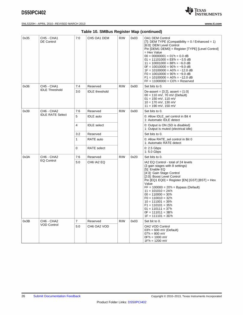
Table 10. SMBus Register Map
Address Register Name Bit (s) Field Type Default Description
Copyright © 2010–2013, Texas Instruments Incorporated Submit Documentation Feedback 19
Product Folder Links: DS50PCI402

DS50PCI402
SNLS320H –APRIL 2010–REVISED MARCH 2013 www.ti.com
Table 10. SMBus Register Map (continued)
0x00 Reset 7:1 Reserved R/W 0x00 Set bits to 0.
0 Reset SMBus Reset1: Reset registers to default value
0x01 PWDN Channels 7:0 PWDN CHx R/W 0x00 Power Down per Channel[7]: CHA_3[6]: CHA_2[5]: CHA_1[4]: CHA_0[3]: CHB_3[2]: CHB_2[1]: CHB_1[0]: CHB_000'h = all channels enabledFF'h = all channels disabled
0x02 PWDN Control 7:1 Reserved R/W 0x00 Set bits to 0.
0 Override PWDN 0: Allow PWDN pin control1: Block PWDN pin control
0x08 Pin Control Override 7:5 Reserved R/W 0x00 Set bits to 0.
4 Override IDLE 0: Allow IDLE pin control1: Block IDLE pin control
3 Reserved Set bit to 0.
2 Override RATE 0: Allow RATE pin control1: Block RATE pin control
1:0 Reserved Set bits to 0.
0x0E CH0 - CHB0 7:6 Reserved R/W 0x00 Set bits to 0.IDLE RATE Select 5 IDLE auto 0: Allow IDLE_sel control in Bit 4
1: Automatic IDLE detect
4 IDLE select 0: Output is ON (SD is disabled)1: Output is muted (electrical idle)
3:2 Reserved Set bits to 0.
1 RATE auto 0: Allow RATE_sel control in Bit 01: Automatic RATE detect
0 RATE select 0: 2.5 Gbps1: 5.0 Gbps
0x0F CH0 - CHB0 7:6 Reserved R/W 0x20 Set bits to 0.EQ Control 5:0 CH0 IB0 EQ IB0 EQ Control - total of 24 levels
(3 gain stages with 8 settings)[5]: Enable EQ[4:3]: Gain Stage Control[2:0]: Boost Level ControlPin [EQ1 EQ0] = Register [EN] [GST] [BST] = HexValueFF = 100000 = 20'h = Bypass (Default)11 = 101010 = 2A'h00 = 110000 = 30'hF0 = 110010 = 32'h10 = 111001 = 39'hF1 = 110101 = 35'h01 = 110111 = 37'h0F = 111011 = 3B'h1F = 111101 = 3D'h
0x10 CH0 - CHB0 7 Reserved R/W 0x03 Set bit to 0.VOD Control 5:0 CH0 OB0 VOD OB0 VOD Control
03'h = 600 mV (Default)07'h = 800 mV0F'h = 1000 mV1F'h = 1200 mV
20 Submit Documentation Feedback Copyright © 2010–2013, Texas Instruments Incorporated
Product Folder Links: DS50PCI402

DS50PCI402
www.ti.com SNLS320H –APRIL 2010–REVISED MARCH 2013
Table 10. SMBus Register Map (continued)
0x11 CH0 - CHB0 7:0 CH0 OB0 DEM R/W 0x03 OB0 DEM ControlDE Control [7]: DEM TYPE (Compatibility = 0 / Enhanced = 1)
[6:0]: DEM Level ControlPin [DEM1 DEM0] = Register [TYPE] [Level Control]= Hex Value00 = 00000001 = 01'h = 0.0 dB01 = 11101000 = E8'h = −3.5 dB11 = 10001000 = 88'h = −6.0 dB0F = 10010000 = 90'h = −9.0 dB1F = 10100000 = A0'h = −12.0 dBF0 = 10010000 = 90'h = −9.0 dBF1 = 10100000 = A0'h = −12.0 dBFF = 11000000 = C0'h = Reserved
0x12 CH0 - CHB0 7:4 Reserved R/W 0x00 Set bits to 0.IDLE Threshold 3:0 IDLE threshold De-assert = [3:2], assert = [1:0]
00 = 110 mV, 70 mV (Default)01 = 150 mV, 110 mV10 = 170 mV, 130 mV11 = 190 mV, 150 mV
0x15 CH1 - CHB1 7:6 Reserved R/W 0x00 Set bits to 0.IDLE RATE Select 5 IDLE auto 0: Allow IDLE_sel control in Bit 4
1: Automatic IDLE detect
4 IDLE select 0: Output is ON (SD is disabled)1: Output is muted (electrical idle)
3:2 Reserved Set bits to 0.
1 RATE auto 0: Allow RATE_sel control in Bit 01: Automatic RATE detect
0 RATE select 0: 2.5 Gbps1: 5.0 Gbps
0x16 CH1 - CHB1 7:6 Reserved R/W 0x20 Set bits to 0.EQ Control 5:0 CH1 IB1 EQ IB1 EQ Control - total of 24 levels
(3 gain stages with 8 settings)[5]: Enable EQ[4:3]: Gain Stage Control[2:0]: Boost Level ControlPin [EQ1 EQ0] = Register [EN] [GST] [BST] = HexValueFF = 100000 = 20'h = Bypass (Default)11 = 101010 = 2A'h00 = 110000 = 30'hF0 = 110010 = 32'h10 = 111001 = 39'hF1 = 110101 = 35'h01 = 110111 = 37'h0F = 111011 = 3B'h1F = 111101 = 3D'h
0x17 CH1 - CHB1 7 Reserved R/W 0x03 Set bit to 0.VOD Control 5:0 CH1 OB1 VOD OB1 VOD Control
03'h = 600 mV (Default)07'h = 800 mV0F'h = 1000 mV1F'h = 1200 mV
Copyright © 2010–2013, Texas Instruments Incorporated Submit Documentation Feedback 21
Product Folder Links: DS50PCI402

DS50PCI402
SNLS320H –APRIL 2010–REVISED MARCH 2013 www.ti.com
Table 10. SMBus Register Map (continued)
0x18 CH1 - CHB1 7:0 CH1 OB1 DEM R/W 0x03 OB1 DEM ControlDE Control [7]: DEM TYPE (Compatibility = 0 / Enhanced = 1)
[6:0]: DEM Level ControlPin [DEM1 DEM0] = Register [TYPE] [Level Control]= Hex Value00 = 00000001 = 01'h = 0.0 dB01 = 11101000 = E8'h = −3.5 dB11 = 10001000 = 88'h = −6.0 dB0F = 10010000 = 90'h = −9.0 dB1F = 10100000 = A0'h = −12.0 dBF0 = 10010000 = 90'h = −9.0 dBF1 = 10100000 = A0'h = −12.0 dBFF = 11000000 = C0'h = Reserved
0x19 CH1 - CHB1 7:4 Reserved R/W 0x00 Set bits to 0.IDLE Threshold 3:0 IDLE threshold De-assert = [3:2], assert = [1:0]
00 = 110 mV, 70 mV (Default)01 = 150 mV, 110 mV10 = 170 mV, 130 mV11 = 190 mV, 150 mV
0x1C CH2 - CHB2 7:6 Reserved R/W 0x00 Set bits to 0.IDLE RATE Select 5 IDLE auto 0: Allow IDLE_sel control in Bit 4
1: Automatic IDLE detect
4 IDLE select 0: Output is ON (SD is disabled)1: Output is muted (electrical idle)
3:2 Reserved Set bits to 0.
1 RATE auto 0: Allow RATE_sel control in Bit 01: Automatic RATE detect
0 RATE select 0: 2.5 Gbps1: 5.0 Gbps
0x1D CH2 - CHB2 7:6 Reserved R/W 0x20 Set bits to 0.EQ Control 5:0 CH2 IB2 EQ IB2 EQ Control - total of 24 levels
(3 gain stages with 8 settings)[5]: Enable EQ[4:3]: Gain Stage Control[2:0]: Boost Level ControlPin [EQ1 EQ0] = Register [EN] [GST] [BST] = HexValueFF = 100000 = 20'h = Bypass (Default)11 = 101010 = 2A'h00 = 110000 = 30'hF0 = 110010 = 32'h10 = 111001 = 39'hF1 = 110101 = 35'h01 = 110111 = 37'h0F = 111011 = 3B'h1F = 111101 = 3D'h
0x1E CH2 - CHB2 7 Reserved R/W 0x03 Set bit to 0.VOD Control 5:0 CH2 OB2 VOD OB2 VOD Control
03'h = 600 mV (Default)07'h = 800 mV0F'h = 1000 mV1F'h = 1200 mV
22 Submit Documentation Feedback Copyright © 2010–2013, Texas Instruments Incorporated
Product Folder Links: DS50PCI402

DS50PCI402
www.ti.com SNLS320H –APRIL 2010–REVISED MARCH 2013
Table 10. SMBus Register Map (continued)
0x1F CH2 - CHB2 7:0 CH2 OB2 DEM R/W 0x03 OB2 DEM ControlDE Control [7]: DEM TYPE (Compatibility = 0 / Enhanced = 1)
[6:0]: DEM Level ControlPin [DEM1 DEM0] = Register [TYPE] [Level Control]= Hex Value00 = 00000001 = 01'h = 0.0 dB01 = 11101000 = E8'h = −3.5 dB11 = 10001000 = 88'h = −6.0 dB0F = 10010000 = 90'h = −9.0 dB1F = 10100000 = A0'h = −12.0 dBF0 = 10010000 = 90'h = −9.0 dBF1 = 10100000 = A0'h = −12.0 dBFF = 11000000 = C0'h = Reserved
0x20 CH2 - CHB2 7:4 Reserved R/W 0x00 Set bits to 0.IDLE Threshold 3:0 IDLE threshold De-assert = [3:2], assert = [1:0]
00 = 110 mV, 70 mV (Default)01 = 150 mV, 110 mV10 = 170 mV, 130 mV11 = 190 mV, 150 mV
0x23 CH3 - CHB3 7:6 Reserved R/W 0x00 Set bits to 0.IDLE RATE Select 5 IDLE auto 0: Allow IDLE_sel control in Bit 4
1: Automatic IDLE detect
4 IDLE select 0: Output is ON (SD is disabled)1: Output is muted (electrical idle)
3:2 Reserved Set bits to 0.
1 RATE auto 0: Allow RATE_sel control in Bit 01: Automatic RATE detect
0 RATE select 0: 2.5 Gbps1: 5.0 Gbps
0x24 CH3 - CHB3 7:6 Reserved R/W 0x20 Set bits to 0.EQ Control 5:0 CH3 IB3 EQ IB3 EQ Control - total of 24 levels
(3 gain stages with 8 settings)[5]: Enable EQ[4:3]: Gain Stage Control[2:0]: Boost Level ControlPin [EQ1 EQ0] = Register [EN] [GST] [BST] = HexValueFF = 100000 = 20'h = Bypass (Default)11 = 101010 = 2A'h00 = 110000 = 30'hF0 = 110010 = 32'h10 = 111001 = 39'hF1 = 110101 = 35'h01 = 110111 = 37'h0F = 111011 = 3B'h1F = 111101 = 3D'h
0x25 CH3 - CHB3 7 Reserved R/W 0x03 Set bit to 0.VOD Control 5:0 CH3 OB3 VOD OB3 VOD Control
03'h = 600 mV (Default)07'h = 800 mV0F'h = 1000 mV1F'h = 1200 mV
Copyright © 2010–2013, Texas Instruments Incorporated Submit Documentation Feedback 23
Product Folder Links: DS50PCI402

DS50PCI402
SNLS320H –APRIL 2010–REVISED MARCH 2013 www.ti.com
Table 10. SMBus Register Map (continued)
0x26 CH3 - CHB3 7:0 CH3 OB3 DEM R/W 0x03 OB3 DEM ControlDE Control [7]: DEM TYPE (Compatibility = 0 / Enhanced = 1)
[6:0]: DEM Level ControlPin [DEM1 DEM0] = Register [TYPE] [Level Control]= Hex Value00 = 00000001 = 01'h = 0.0 dB01 = 11101000 = E8'h = −3.5 dB11 = 10001000 = 88'h = −6.0 dB0F = 10010000 = 90'h = −9.0 dB1F = 10100000 = A0'h = −12.0 dBF0 = 10010000 = 90'h = −9.0 dBF1 = 10100000 = A0'h = −12.0 dBFF = 11000000 = C0'h = Reserved
0x27 CH3 - CHB3 7:4 Reserved R/W 0x00 Set bits to 0.IDLE Threshold 3:0 IDLE threshold De-assert = [3:2], assert = [1:0]
00 = 110 mV, 70 mV (Default)01 = 150 mV, 110 mV10 = 170 mV, 130 mV11 = 190 mV, 150 mV
0x2B CH4 - CHA0 7:6 Reserved R/W 0x00 Set bits to 0.IDLE RATE Select 5 IDLE auto 0: Allow IDLE_sel control in Bit 4
1: Automatic IDLE detect
4 IDLE select 0: Output is ON (SD is disabled)1: Output is muted (electrical idle)
3:2 Reserved Set bits to 0.
1 RATE auto 0: Allow RATE_sel control in Bit 01: Automatic RATE detect
0 RATE select 0: 2.5 Gbps1: 5.0 Gbps
0x2C CH4 - CHA0 7:6 Reserved R/W 0x20 Set bits to 0.EQ Control 5:0 CH4 IA0 EQ IA0 EQ Control - total of 24 levels
(3 gain stages with 8 settings)[5]: Enable EQ[4:3]: Gain Stage Control[2:0]: Boost Level ControlPin [EQ1 EQ0] = Register [EN] [GST] [BST] = HexValueFF = 100000 = 20'h = Bypass (Default)11 = 101010 = 2A'h00 = 110000 = 30'hF0 = 110010 = 32'h10 = 111001 = 39'hF1 = 110101 = 35'h01 = 110111 = 37'h0F = 111011 = 3B'h1F = 111101 = 3D'h
0x2D CH4 - CHA0 7 Reserved R/W 0x03 Set bit to 0.VOD Control 5:0 CH4 OA0 VOD OA0 VOD Control
03'h = 600 mV (Default)07'h = 800 mV0F'h = 1000 mV1F'h = 1200 mV
24 Submit Documentation Feedback Copyright © 2010–2013, Texas Instruments Incorporated
Product Folder Links: DS50PCI402

DS50PCI402
www.ti.com SNLS320H –APRIL 2010–REVISED MARCH 2013
Table 10. SMBus Register Map (continued)
0x2E CH4 - CHA0 7:0 CH4 OA0 DEM R/W 0x03 OA0 DEM ControlDE Control [7]: DEM TYPE (Compatibility = 0 / Enhanced = 1)
[6:0]: DEM Level ControlPin [DEM1 DEM0] = Register [TYPE] [Level Control]= Hex Value00 = 00000001 = 01'h = 0.0 dB01 = 11101000 = E8'h = −3.5 dB11 = 10001000 = 88'h = −6.0 dB0F = 10010000 = 90'h = −9.0 dB1F = 10100000 = A0'h = −12.0 dBF0 = 10010000 = 90'h = −9.0 dBF1 = 10100000 = A0'h = −12.0 dBFF = 11000000 = C0'h = Reserved
0x2F CH4 - CHA0 7:4 Reserved R/W 0x00 Set bits to 0.IDLE Threshold 3:0 IDLE threshold De-assert = [3:2], assert = [1:0]
00 = 110 mV, 70 mV (Default)01 = 150 mV, 110 mV10 = 170 mV, 130 mV11 = 190 mV, 150 mV
0x32 CH5 - CHA1 7:6 Reserved R/W 0x00 Set bits to 0.IDLE RATE Select 5 IDLE auto 0: Allow IDLE_sel control in Bit 4
1: Automatic IDLE detect
4 IDLE select 0: Output is ON (SD is disabled)1: Output is muted (electrical idle)
3:2 Reserved Set bits to 0.
1 RATE auto 0: Allow RATE_sel control in Bit 01: Automatic RATE detect
0 RATE select 0: 2.5 Gbps1: 5.0 Gbps
0x33 CH5 - CHA1 7:6 Reserved R/W 0x20 Set bits to 0.EQ Control 5:0 CH5 IA1 EQ IA1 EQ Control - total of 24 levels
(3 gain stages with 8 settings)[5]: Enable EQ[4:3]: Gain Stage Control[2:0]: Boost Level ControlPin [EQ0 EQ1] = Register [EN] [GST] [BST] = HexValueFF = 100000 = 20'h = Bypass (Default)11 = 101010 = 2A'h00 = 110000 = 30'hF0 = 110010 = 32'h10 = 111001 = 39'hF1 = 110101 = 35'h01 = 110111 = 37'h0F = 111011 = 3B'h1F = 111101 = 3D'h
0x34 CH5 - CHA1 7 Reserved R/W 0x03 Set bit to 0.VOD Control 5:0 CH5 OA1 VOD OA1 VOD Control
03'h = 600 mV (Default)07'h = 800 mV0F'h = 1000 mV1F'h = 1200 mV
Copyright © 2010–2013, Texas Instruments Incorporated Submit Documentation Feedback 25
Product Folder Links: DS50PCI402
DS50PCI402
SNLS320H –APRIL 2010–REVISED MARCH 2013 www.ti.com
Table 10. SMBus Register Map (continued)
0x35 CH5 - CHA1 7:0 CH5 OA1 DEM R/W 0x03 OA1 DEM ControlDE Control [7]: DEM TYPE (Compatibility = 0 / Enhanced = 1)
[6:0]: DEM Level ControlPin [DEM1 DEM0] = Register [TYPE] [Level Control]= Hex Value00 = 00000001 = 01'h = 0.0 dB01 = 11101000 = E8'h = −3.5 dB11 = 10001000 = 88'h = −6.0 dB0F = 10010000 = 90'h = −9.0 dB1F = 10100000 = A0'h = −12.0 dBF0 = 10010000 = 90'h = −9.0 dBF1 = 10100000 = A0'h = −12.0 dBFF = 11000000 = C0'h = Reserved
0x36 CH5 - CHA1 7:4 Reserved R/W 0x00 Set bits to 0.IDLE Threshold 3:0 IDLE threshold De-assert = [3:2], assert = [1:0]
00 = 110 mV, 70 mV (Default)01 = 150 mV, 110 mV10 = 170 mV, 130 mV11 = 190 mV, 150 mV
0x39 CH6 - CHA2 7:6 Reserved R/W 0x00 Set bits to 0.IDLE RATE Select 5 IDLE auto 0: Allow IDLE_sel control in Bit 4
1: Automatic IDLE detect
4 IDLE select 0: Output is ON (SD is disabled)1: Output is muted (electrical idle)
3:2 Reserved Set bits to 0.
1 RATE auto 0: Allow RATE_sel control in Bit 01: Automatic RATE detect
0 RATE select 0: 2.5 Gbps1: 5.0 Gbps
0x3A CH6 - CHA2 7:6 Reserved R/W 0x20 Set bits to 0.EQ Control 5:0 CH6 IA2 EQ IA2 EQ Control - total of 24 levels
(3 gain stages with 8 settings)[5]: Enable EQ[4:3]: Gain Stage Control[2:0]: Boost Level ControlPin [EQ1 EQ0] = Register [EN] [GST] [BST] = HexValueFF = 100000 = 20'h = Bypass (Default)11 = 101010 = 2A'h00 = 110000 = 30'hF0 = 110010 = 32'h10 = 111001 = 39'hF1 = 110101 = 35'h01 = 110111 = 37'h0F = 111011 = 3B'h1F = 111101 = 3D'h
0x3B CH6 - CHA2 7 Reserved R/W 0x03 Set bit to 0.VOD Control 5:0 CH6 OA2 VOD OA2 VOD Control
03'h = 600 mV (Default)07'h = 800 mV0F'h = 1000 mV1F'h = 1200 mV
26 Submit Documentation Feedback Copyright © 2010–2013, Texas Instruments Incorporated
Product Folder Links: DS50PCI402

DS50PCI402
www.ti.com SNLS320H –APRIL 2010–REVISED MARCH 2013
Table 10. SMBus Register Map (continued)
0x3C CH6 - CHA2 7:0 CH6 OA2 DEM R/W 0x03 OA2 DEM ControlDE Control [7]: DEM TYPE (Compatibility = 0 / Enhanced = 1)
[6:0]: DEM Level ControlPin [DEM1 DEM0] = Register [TYPE] [Level Control]= Hex Value00 = 00000001 = 01'h = 0.0 dB01 = 11101000 = E8'h = −3.5 dB11 = 10001000 = 88'h = −6.0 dB0F = 10010000 = 90'h = −9.0 dB1F = 10100000 = A0'h = −12.0 dBF0 = 10010000 = 90'h = −9.0 dBF1 = 10100000 = A0'h = −12.0 dBFF = 11000000 = C0'h = Reserved
0x3D CH6 - CHA2 7:4 Reserved R/W 0x00 Set bits to 0.IDLE Threshold 3:0 IDLE threshold De-assert = [3:2], assert = [1:0]
00 = 110 mV, 70 mV (Default)01 = 150 mV, 110 mV10 = 170 mV, 130 mV11 = 190 mV, 150 mV
0x40 CH7 - CHA3 7:6 Reserved R/W 0x00 Set bits to 0.IDLE RATE Select 5 IDLE auto 0: Allow IDLE_sel control in Bit 4
1: Automatic IDLE detect
4 IDLE select 0: Output is ON (SD is disabled)1: Output is muted (electrical idle)
3:2 Reserved Set bits to 0.
1 RATE auto 0: Allow RATE_sel control in Bit 01: Automatic RATE detect
0 RATE select 0: 2.5 Gbps1: 5.0 Gbps
0x41 CH7 - CHA3 7:6 Reserved R/W 0x20 Set bits to 0.EQ Control 5:0 CH7 IA3 EQ IA3 EQ Control - total of 24 levels
(3 gain stages with 8 settings)[5]: Enable EQ[4:3]: Gain Stage Control[2:0]: Boost Level ControlPin [EQ0 EQ1] = Register [EN] [GST] [BST] = HexValueFF = 100000 = 20'h = Bypass (Default)11 = 101010 = 2A'h00 = 110000 = 30'hF0 = 110010 = 32'h10 = 111001 = 39'hF1 = 110101 = 35'h01 = 110111 = 37'h0F = 111011 = 3B'h1F = 111101 = 3D'h
0x42 CH7 - CHA3 7 Reserved R/W 0x03 Set bit to 0.VOD Control 5:0 CH7 OA3 VOD OA3 VOD Control
03'h = 600 mV (Default)07'h = 800 mV0F'h = 1000 mV1F'h = 1200 mV
Copyright © 2010–2013, Texas Instruments Incorporated Submit Documentation Feedback 27
Product Folder Links: DS50PCI402

DS50PCI402
SNLS320H –APRIL 2010–REVISED MARCH 2013 www.ti.com
Table 10. SMBus Register Map (continued)
0x43 CH7 - CHA3 7:0 CH7 OA3 DEM R/W 0x03 OA3 DEM ControlDE Control [7]: DEM TYPE (Compatibility = 0 / Enhanced = 1)
[6:0]: DEM Level ControlPin [DEM1 DEM0] = Register [TYPE] [Level Control]= Hex Value00 = 00000001 = 01'h = 0.0 dB01 = 11101000 = E8'h = −3.5 dB11 = 10001000 = 88'h = −6.0 dB0F = 10010000 = 90'h = −9.0 dB1F = 10100000 = A0'h = −12.0 dBF0 = 10010000 = 90'h = −9.0 dBF1 = 10100000 = A0'h = −12.0 dBFF = 11000000 = C0'h = Reserved
0x44 CH7 - CHA3 7:4 Reserved R/W 0x00 Set bits to 0.IDLE Threshold 3:0 IDLE threshold De-assert = [3:2], assert = [1:0]
00 = 110 mV, 70 mV (Default)01 = 150 mV, 110 mV10 = 170 mV, 130 mV11 = 190 mV, 150 mV
0x47 Global VOD Adjust 7:2 Reserved R/W 0x02 Set bits to 0.
1:0 VOD Adjust 00 = -25.0%01 = -12.5%10 = +0.0% (Default)11 = +12.5%
28 Submit Documentation Feedback Copyright © 2010–2013, Texas Instruments Incorporated
Product Folder Links: DS50PCI402

46
47
48
49
50
51
52
53
54
4342414039383736
22
27
26
25
24
23
21
20
19
4544
345678910 12
GNDBOTTOM OF PKG
131415161718 1112
333231302928 3534
VDD
VDD
VDD
VDD
100 mils
20 mils
20 mils
VDD
INTERNAL STRIPLINE
EXTERNAL MICROSTRIP
DS50PCI402
www.ti.com SNLS320H –APRIL 2010–REVISED MARCH 2013
APPLICATION INFORMATION
GENERAL RECOMMENDATIONS
The DS50PCI402 is a high performance circuit capable of delivering excellent performance. Careful attentionmust be paid to the details associated with high-speed design as well as providing a clean power supply. Referto the information below and the latest version of the LVDS Owner's Manual for more detailed information onhigh speed design tips to address signal integrity design issues.
PCB LAYOUT CONSIDERATIONS FOR DIFFERENTIAL PAIRS
The CML inputs and LPDS outputs have been optimized to work with interconnects using a controlled differentialimpedance of 85 - 100Ω. It is preferable to route differential lines exclusively on one layer of the board,particularly for the input traces. The use of vias should be avoided if possible. If vias must be used, they shouldbe used sparingly and must be placed symmetrically for each side of a given differential pair. Wheneverdifferential vias are used the layout must also provide for a low inductance path for the return currents as well.Route the differential signals away from other signals and noise sources on the printed circuit board. See AN-1187 (SNOA401) for additional information on WQFN packages.
Figure 8. Typical Routing Options
The graphic shown above depicts different transmission line topologies which can be used in variouscombinations to achieve the optimal system performance. Impedance discontinuities at the differential via can beminimized or eliminated by increasing the swell around each hole and providing for a low inductance returncurrent path. When the via structure is associated with thick backplane PCB, further optimization such as backdrilling is often used to reduce the deterimential high frequency effects of stubs on the signal path.
Copyright © 2010–2013, Texas Instruments Incorporated Submit Documentation Feedback 29
Product Folder Links: DS50PCI402

-RLTX-DIFF (SDD11)
-40
-35
-30
-25
-20
-15
-10
-5
0
0.00 0.50 1.00 1.50 2.00 2.50
S11
Frequency (GHz)
-RLTX-CM (S11)
SDD11Ret
urn
Lo
ss (
dB
)
-RLRX-DIFF (SDD11)
-40
-35
-30
-25
-20
-15
-10
-5
0
0.00 0.50 1.00 1.50 2.00 2.50
S11
Frequency (GHz)
-RLRX-CM (S11)
SDD11
Ret
urn
Lo
ss (
dB
)
DS50PCI402
SNLS320H –APRIL 2010–REVISED MARCH 2013 www.ti.com
POWER SUPPLY BYPASSING
Two approaches are recommended to ensure that the DS50PCI402 is provided with an adequate power supply.First, the supply (VDD) and ground (GND) pins should be connected to power planes routed on adjacent layersof the printed circuit board. The layer thickness of the dielectric should be minimized so that the VDD and GNDplanes create a low inductance supply with distributed capacitance. Second, careful attention to supplybypassing through the proper use of bypass capacitors is required. A 0.01 μF bypass capacitor should beconnected to each VDD pin such that the capacitor is placed as close as possible to the DS50PCI402. Smallerbody size capacitors can help facilitate proper component placement. Additionally, three capacitors withcapacitance in the range of 2.2 μF to 10 μF should be incorporated in the power supply bypassing design aswell. These capacitors can be either tantalum or an ultra-low ESR ceramic.
Typical Performance Eye Diagrams and Curves
DS50PCI402 Return Loss
Figure 9. Receiver Return Loss Mask for 5.0 Gbps
Figure 10. Transmitter Return Loss Mask for 5.0 Gbps
30 Submit Documentation Feedback Copyright © 2010–2013, Texas Instruments Incorporated
Product Folder Links: DS50PCI402

DS50PCI402
www.ti.com SNLS320H –APRIL 2010–REVISED MARCH 2013
REVISION HISTORY
Changes from Revision G (March 2013) to Revision H Page
• Changed layout of National Data Sheet to TI format .......................................................................................................... 30
Copyright © 2010–2013, Texas Instruments Incorporated Submit Documentation Feedback 31
Product Folder Links: DS50PCI402

PACKAGE OPTION ADDENDUM
www.ti.com 11-Apr-2013
Addendum-Page 1
PACKAGING INFORMATION
Orderable Device Status(1)
Package Type PackageDrawing
Pins PackageQty
Eco Plan(2)
Lead/Ball Finish MSL Peak Temp(3)
Op Temp (°C) Top-Side Markings(4)
Samples
DS50PCI402SQ/NOPB ACTIVE WQFN NJY 54 2000 Green (RoHS& no Sb/Br)
CU SN Level-2-260C-1 YEAR -10 to 85 DS50PCI402SQ
DS50PCI402SQE/NOPB ACTIVE WQFN NJY 54 250 Green (RoHS& no Sb/Br)
CU SN Level-2-260C-1 YEAR -10 to 85 DS50PCI402SQ
(1) The marketing status values are defined as follows:ACTIVE: Product device recommended for new designs.LIFEBUY: TI has announced that the device will be discontinued, and a lifetime-buy period is in effect.NRND: Not recommended for new designs. Device is in production to support existing customers, but TI does not recommend using this part in a new design.PREVIEW: Device has been announced but is not in production. Samples may or may not be available.OBSOLETE: TI has discontinued the production of the device.
(2) Eco Plan - The planned eco-friendly classification: Pb-Free (RoHS), Pb-Free (RoHS Exempt), or Green (RoHS & no Sb/Br) - please check http://www.ti.com/productcontent for the latest availabilityinformation and additional product content details.TBD: The Pb-Free/Green conversion plan has not been defined.Pb-Free (RoHS): TI's terms "Lead-Free" or "Pb-Free" mean semiconductor products that are compatible with the current RoHS requirements for all 6 substances, including the requirement thatlead not exceed 0.1% by weight in homogeneous materials. Where designed to be soldered at high temperatures, TI Pb-Free products are suitable for use in specified lead-free processes.Pb-Free (RoHS Exempt): This component has a RoHS exemption for either 1) lead-based flip-chip solder bumps used between the die and package, or 2) lead-based die adhesive used betweenthe die and leadframe. The component is otherwise considered Pb-Free (RoHS compatible) as defined above.Green (RoHS & no Sb/Br): TI defines "Green" to mean Pb-Free (RoHS compatible), and free of Bromine (Br) and Antimony (Sb) based flame retardants (Br or Sb do not exceed 0.1% by weightin homogeneous material)
(3) MSL, Peak Temp. -- The Moisture Sensitivity Level rating according to the JEDEC industry standard classifications, and peak solder temperature.
(4) Multiple Top-Side Markings will be inside parentheses. Only one Top-Side Marking contained in parentheses and separated by a "~" will appear on a device. If a line is indented then it is acontinuation of the previous line and the two combined represent the entire Top-Side Marking for that device.
Important Information and Disclaimer:The information provided on this page represents TI's knowledge and belief as of the date that it is provided. TI bases its knowledge and belief on informationprovided by third parties, and makes no representation or warranty as to the accuracy of such information. Efforts are underway to better integrate information from third parties. TI has taken andcontinues to take reasonable steps to provide representative and accurate information but may not have conducted destructive testing or chemical analysis on incoming materials and chemicals.TI and TI suppliers consider certain information to be proprietary, and thus CAS numbers and other limited information may not be available for release.
In no event shall TI's liability arising out of such information exceed the total purchase price of the TI part(s) at issue in this document sold by TI to Customer on an annual basis.

TAPE AND REEL INFORMATION
*All dimensions are nominal
Device PackageType
PackageDrawing
Pins SPQ ReelDiameter
(mm)
ReelWidth
W1 (mm)
A0(mm)
B0(mm)
K0(mm)
P1(mm)
W(mm)
Pin1Quadrant
DS50PCI402SQ/NOPB WQFN NJY 54 2000 330.0 16.4 5.8 10.3 1.0 12.0 16.0 Q1
DS50PCI402SQE/NOPB WQFN NJY 54 250 178.0 16.4 5.8 10.3 1.0 12.0 16.0 Q1
PACKAGE MATERIALS INFORMATION
www.ti.com 20-Sep-2016
Pack Materials-Page 1

*All dimensions are nominal
Device Package Type Package Drawing Pins SPQ Length (mm) Width (mm) Height (mm)
DS50PCI402SQ/NOPB WQFN NJY 54 2000 367.0 367.0 38.0
DS50PCI402SQE/NOPB WQFN NJY 54 250 210.0 185.0 35.0
PACKAGE MATERIALS INFORMATION
www.ti.com 20-Sep-2016
Pack Materials-Page 2
www.ti.com
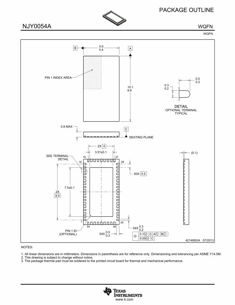
PACKAGE OUTLINE
C
54X 0.30.2
3.51±0.1
50X 0.5
54X 0.50.3
0.8 MAX
2X8.5
7.5±0.1
2X 4
A
10.19.9
B 5.65.4
0.30.2
0.50.3
(0.1)
4214993/A 07/2013
WQFNNJY0054AWQFN
PIN 1 INDEX AREA
SEATING PLANE
1
18 28
45
19 27
54 46
0.1 C A B0.05 C
(OPTIONAL)PIN 1 ID
DETAILSEE TERMINAL
NOTES: 1. All linear dimensions are in millimeters. Dimensions in parenthesis are for reference only. Dimensioning and tolerancing per ASME Y14.5M.2. This drawing is subject to change without notice. 3. The package thermal pad must be soldered to the printed circuit board for thermal and mechanical performance.
SCALE 2.000
DETAILOPTIONAL TERMINAL
TYPICAL

www.ti.com
EXAMPLE BOARD LAYOUT
(3.51)
0.07 MINALL AROUND
0.07 MAXALL AROUND
54X (0.6)
54X (0.25)
(9.8)
(5.3)
( ) TYPVIA
0.2
50X (0.5)
2X(1.16)
(1) TYP
(7.5)
(1.17)TYP
4214993/A 07/2013
WQFNNJY0054AWQFN
SYMMSEE DETAILS
1
18
19 27
28
45
4654
SYMM
LAND PATTERN EXAMPLESCALE:8X
NOTES: (continued) 4. This package is designed to be soldered to a thermal pad on the board. For more information, refer to QFN/SON PCB application note in literature No. SLUA271 (www.ti.com/lit/slua271).
SOLDER MASKOPENING
METAL
SOLDER MASKDEFINED
METAL
SOLDER MASKOPENING
SOLDER MASK DETAILS
NON SOLDER MASKDEFINED
(PREFERRED)
www.ti.com
EXAMPLE STENCIL DESIGN
(1.17)TYP
(5.3)
54X (0.6)
54X (0.25)
12X (1.51)
(9.8)
(0.855) TYP
12X (0.97)
50X (0.5)
4214993/A 07/2013
WQFNNJY0054AWQFN
NOTES: (continued) 5. Laser cutting apertures with trapezoidal walls and rounded corners may offer better paste release. IPC-7525 may have alternate design recommendations.
SYMM
TYPMETAL
SOLDERPASTE EXAMPLEBASED ON 0.125mm THICK STENCIL
EXPOSED PAD
67% PRINTED SOLDER COVERAGE BY AREASCALE:10X
1
18
19 27
28
45
4654
SYMM

IMPORTANT NOTICE
Texas Instruments Incorporated and its subsidiaries (TI) reserve the right to make corrections, enhancements, improvements and otherchanges to its semiconductor products and services per JESD46, latest issue, and to discontinue any product or service per JESD48, latestissue. Buyers should obtain the latest relevant information before placing orders and should verify that such information is current andcomplete. All semiconductor products (also referred to herein as “components”) are sold subject to TI’s terms and conditions of salesupplied at the time of order acknowledgment.TI warrants performance of its components to the specifications applicable at the time of sale, in accordance with the warranty in TI’s termsand conditions of sale of semiconductor products. Testing and other quality control techniques are used to the extent TI deems necessaryto support this warranty. Except where mandated by applicable law, testing of all parameters of each component is not necessarilyperformed.TI assumes no liability for applications assistance or the design of Buyers’ products. Buyers are responsible for their products andapplications using TI components. To minimize the risks associated with Buyers’ products and applications, Buyers should provideadequate design and operating safeguards.TI does not warrant or represent that any license, either express or implied, is granted under any patent right, copyright, mask work right, orother intellectual property right relating to any combination, machine, or process in which TI components or services are used. Informationpublished by TI regarding third-party products or services does not constitute a license to use such products or services or a warranty orendorsement thereof. Use of such information may require a license from a third party under the patents or other intellectual property of thethird party, or a license from TI under the patents or other intellectual property of TI.Reproduction of significant portions of TI information in TI data books or data sheets is permissible only if reproduction is without alterationand is accompanied by all associated warranties, conditions, limitations, and notices. TI is not responsible or liable for such altereddocumentation. Information of third parties may be subject to additional restrictions.Resale of TI components or services with statements different from or beyond the parameters stated by TI for that component or servicevoids all express and any implied warranties for the associated TI component or service and is an unfair and deceptive business practice.TI is not responsible or liable for any such statements.Buyer acknowledges and agrees that it is solely responsible for compliance with all legal, regulatory and safety-related requirementsconcerning its products, and any use of TI components in its applications, notwithstanding any applications-related information or supportthat may be provided by TI. Buyer represents and agrees that it has all the necessary expertise to create and implement safeguards whichanticipate dangerous consequences of failures, monitor failures and their consequences, lessen the likelihood of failures that might causeharm and take appropriate remedial actions. Buyer will fully indemnify TI and its representatives against any damages arising out of the useof any TI components in safety-critical applications.In some cases, TI components may be promoted specifically to facilitate safety-related applications. With such components, TI’s goal is tohelp enable customers to design and create their own end-product solutions that meet applicable functional safety standards andrequirements. Nonetheless, such components are subject to these terms.No TI components are authorized for use in FDA Class III (or similar life-critical medical equipment) unless authorized officers of the partieshave executed a special agreement specifically governing such use.Only those TI components which TI has specifically designated as military grade or “enhanced plastic” are designed and intended for use inmilitary/aerospace applications or environments. Buyer acknowledges and agrees that any military or aerospace use of TI componentswhich have not been so designated is solely at the Buyer's risk, and that Buyer is solely responsible for compliance with all legal andregulatory requirements in connection with such use.TI has specifically designated certain components as meeting ISO/TS16949 requirements, mainly for automotive use. In any case of use ofnon-designated products, TI will not be responsible for any failure to meet ISO/TS16949.
Products ApplicationsAudio www.ti.com/audio Automotive and Transportation www.ti.com/automotiveAmplifiers amplifier.ti.com Communications and Telecom www.ti.com/communicationsData Converters dataconverter.ti.com Computers and Peripherals www.ti.com/computersDLP® Products www.dlp.com Consumer Electronics www.ti.com/consumer-appsDSP dsp.ti.com Energy and Lighting www.ti.com/energyClocks and Timers www.ti.com/clocks Industrial www.ti.com/industrialInterface interface.ti.com Medical www.ti.com/medicalLogic logic.ti.com Security www.ti.com/securityPower Mgmt power.ti.com Space, Avionics and Defense www.ti.com/space-avionics-defenseMicrocontrollers microcontroller.ti.com Video and Imaging www.ti.com/videoRFID www.ti-rfid.comOMAP Applications Processors www.ti.com/omap TI E2E Community e2e.ti.comWireless Connectivity www.ti.com/wirelessconnectivity
Mailing Address: Texas Instruments, Post Office Box 655303, Dallas, Texas 75265Copyright © 2016, Texas Instruments Incorporated