Embed Size (px)
Citation preview

MICRO-461Low-power Radio Design for the IoT
5. Modeling of active and passive devices at RF
Passive Devices
Christian EnzIntegrated Circuits Lab (ICLAB), Institute of Microengineering (IMT), School of Engineering (STI)
Swiss Federal Institute of Technology, Lausanne (EPFL), Switzerland

ICLAB
Outline Introduction
Inductors
Transformers
Varactors
© C. Enz | 2021 Low-power radio design for the IoT Slide 1

Introduction
ICLAB
Introduction
Reduction of off-chip components translates into a reduction of system cost
Modeling issues of off-chip inductors
The bond wires and package pins connecting chip to outside world may experience significant coupling
© C. Enz | 2021 Low-power radio design for the IoT Slide 2

ICLAB
Outline Introduction
Inductors
Transformers
Varactors
© C. Enz | 2021 Low-power radio design for the IoT Slide 3

Inductors
ICLAB
Basic Planar Inductor Structure
Has mutual coupling between every two turns and larger inductance than straight wire
Spiral is implemented on top metal layer to minimize parasitic resistance and capacitance
Inductance of an 𝑁-turn planar spiral structure inductor has 𝑁 𝑁 1 2⁄ terms
Factors that limit the growth rate of an inductance of spiral inductor as function of 𝑁: Due to planar geometry the inner turns have smaller size and exhibit smaller inductance. The mutual coupling factor is about 0.7 for adjacent turns hence contributing to lower
inductance.
© C. Enz | 2021 Low-power radio design for the IoT Slide 4
1 2 3 12 13 23totL L L L M M M

Inductors
ICLAB
Geometry of Inductor Effects Inductance A two dimensional square spiral
inductor is fully specified by following four quantities: Outer dimension, 𝐷 Line width, 𝑊 Line spacing, 𝑆 Number of turns, 𝑁
© C. Enz | 2021 Low-power radio design for the IoT Slide 5
Various dimensions of a spiral inductor

Inductors
ICLAB
Effect of Doubling Line Width of Inductor
Doubling the width inevitably decreases the diameter of inner turn, thus lowering their inductance
The spacing between the legs reduces, hence their mutual inductance also decrease
© C. Enz | 2021 Low-power radio design for the IoT Slide 6
Inductors
ICLAB
Magnetic Coupling Factor Plot
Coupling factor between 2 straight metal lines as a function of their normalized spacing 𝑆 𝑊⁄
Obtained from electromagnetic field simulations
© C. Enz | 2021 Low-power radio design for the IoT Slide 7

Inductors
ICLAB
Inductor Structures Encountered in RFIC Design
Various inductor geometries shown above are result of improving the trade-offs in inductor design, specifically those between: The quality factor and the capacitance The inductance and the dimensions
Note that these various inductor geometries provide additional degrees of freedom but also complicate the modeling task
© C. Enz | 2021 Low-power radio design for the IoT Slide 8
Octagonal Symmetric
Stacked With Grounded shield Parallel Spirals
Circular
Inductors
ICLAB
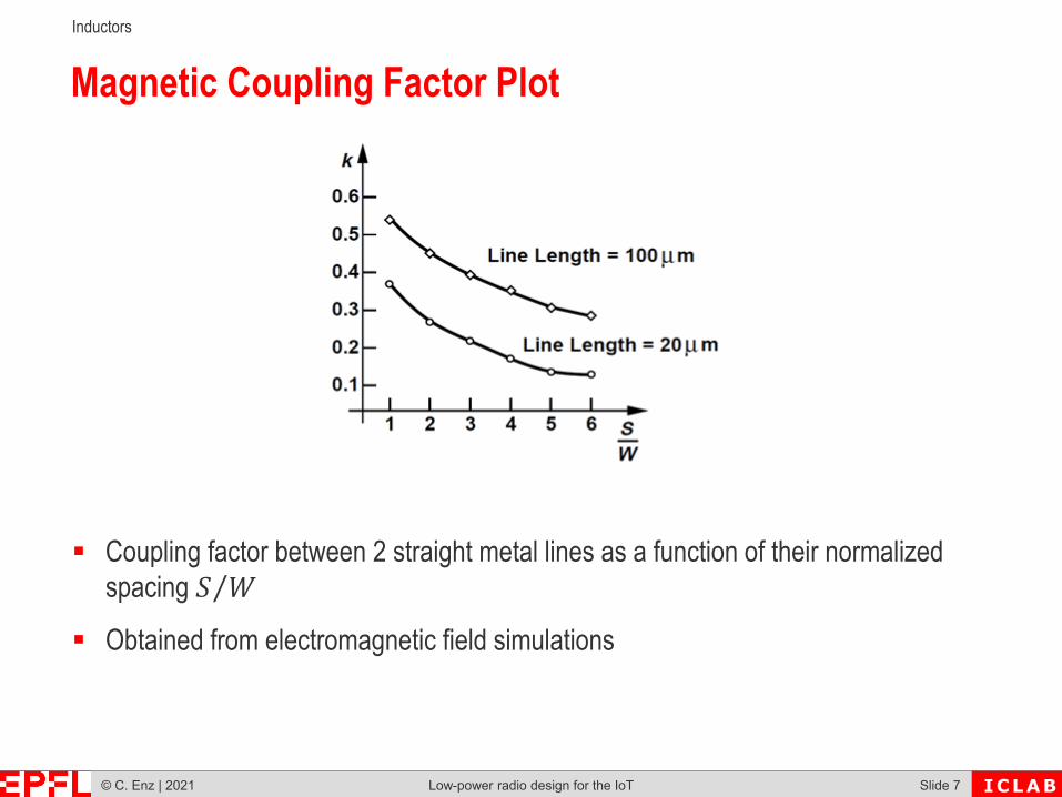
Inductance Equations Closed form inductance equations can be found based on Curve fitting methods Physical properties of inductors
Various expressions have been reported in literature [1,2,3]. For example, an empirical formula that has less than 10% error for inductors in the range of 5 to 50 nH is given in [1] and can be reduced to the following form for a square spiral
Where 𝐴 is the metal area (the shaded area) and 𝐴 ≅ 𝐷 is the total inductor area
All units are metric
© C. Enz | 2021 Low-power radio design for the IoT Slide 9
Inductors
ICLAB
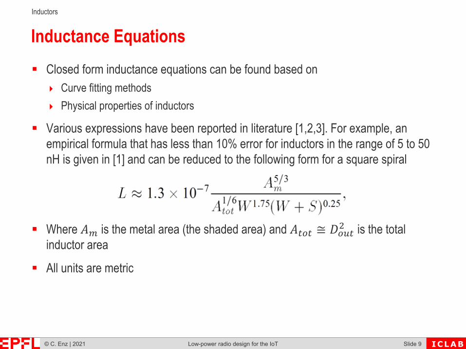
Parasitic Capacitance of Integrated Inductors
Planar spiral inductor suffers from parasitic capacitance because the metal lines of the inductor exhibit parallel plate capacitance and adjacent turns bear fringcapacitance
© C. Enz | 2021 Low-power radio design for the IoT Slide 10

Inductors
ICLAB
Loss Mechanisms: Metal Resistance
Suppose the metal line forming an inductor exhibits a series resistance, 𝑅
The 𝑄 may be defined as the ratio of the desirable impedance, 𝜔 𝐿 , and the undesirable impedance, 𝑅 :
© C. Enz | 2021 Low-power radio design for the IoT Slide 11
For example, a 5-nH inductor operating at 5 GHz with an 𝑅 of 15.7Ω has a Q of 10

Inductors
ICLAB
Loss Mechanisms – Skin Effect
The skin depth 𝛿 is given by
© C. Enz | 2021 Low-power radio design for the IoT Slide 12
Current distribution in a conductor
At low frequency At high frequency
1f
where 𝑓 denotes the frequency, 𝜇 the permeability, and 𝜎 the conductivity. For example, δ ≈ 1.4μm at 10 GHz for aluminum. The extra resistance of a conductor due to the skin effect is equal to
1skinR

Inductors
ICLAB
Skin Effect – Current Crowding Effect
For 𝑓 𝑓 , the magnetic field produced by adjacent turn induces eddy current, causing unequal distribution of current across the conductor width, hence altering the effective resistance of the turn
For 𝑓 𝑓 , the effective resistance 𝑅 therefore increases according to
© C. Enz | 2021 Low-power radio design for the IoT Slide 13
Current distribution in adjacent turns Detailed view of (a)
2
0 21 3.1110 2
witheff critcrit
f W SR R f Rf W
Where 𝑅◻ represents the dc sheet resistance of the metal

Inductors
ICLAB
Capacitive Coupling to Substrate
Voltage at each point of the spiral rise and fall with time causing displacement current flow between this capacitance and substrate
This current causes loss and reduces the Q of the inductor
© C. Enz | 2021 Low-power radio design for the IoT Slide 14
Substrate loss due to capacitive coupling
Inductors
ICLAB
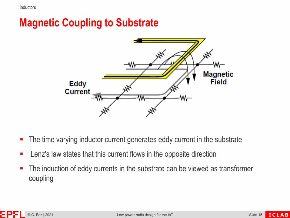
Magnetic Coupling to Substrate
The time varying inductor current generates eddy current in the substrate
Lenz's law states that this current flows in the opposite direction
The induction of eddy currents in the substrate can be viewed as transformer coupling
© C. Enz | 2021 Low-power radio design for the IoT Slide 15

Inductors
ICLAB
Modeling Loss by Series or Parallel Resistor
A constant series resistance 𝑅 model inductor loss for limited range of frequencies
A constant parallel resistance 𝑅 model inductor loss for narrow range of frequencies
Note that the behavior of 𝑄 of inductor predicted by above two models has suggested opposite trends of 𝑄 with frequency
© C. Enz | 2021 Low-power radio design for the IoT Slide 16
1
S
LQR
1
pRQL

Inductors
ICLAB
Modeling Loss by Both Series and Parallel Resistors
The overall Q of the inductor is then given by
© C. Enz | 2021 Low-power radio design for the IoT Slide 17
Modeling loss by both parallel and series resistances Resulting behavior of Q
112
2andS p
LR R Q LQ
1
2 21
p
S S p
R LQ
L R R R
Which shows a maximum at 𝑅 𝑅 𝐿

Inductors
ICLAB
Symmetric Inductor
Differential circuits can employ a single symmetric inductor instead of two asymmetric inductors
It has two advantages: Save area Differential geometry also exhibit higher 𝑄
© C. Enz | 2021 Low-power radio design for the IoT Slide 18

Inductors
ICLAB
Mirror/Step Symmetry of Single Ended Inductor
Lower 𝑄 Higher 𝑄
© C. Enz | 2021 Low-power radio design for the IoT Slide 19
Load inductors in a differential pair
Mirror symmetry Step symmetry
1 2 2eqL L L M 1 2 2eqL L L M

Inductors
ICLAB
Inductors with Ground Shield
This structure allows the displacement current to flow through the low resistance path to ground to avoid electrical loss through substrate
Eddy currents through a continuous shield drastically reduce inductance and 𝑄, so a “patterned” shield is used
This shield reduces the effect of capacitive coupling to substrate
Eddy currents of magnetic coupling still flows through substrate
© C. Enz | 2021 Low-power radio design for the IoT Slide 20

Inductors
ICLAB
Stacked Inductors
Similarly, 𝑁 stacked spiral inductor operating in series raises total inductance by a factor of 𝑁
© C. Enz | 2021 Low-power radio design for the IoT Slide 21
1 2
1 2
2
4
tot
tot
L L L MM L LL L

ICLAB
Outline Introduction
Inductors
Transformers
Varactors
© C. Enz | 2021 Low-power radio design for the IoT Slide 22

Transformers
ICLAB
TransformersUseful function of transformer in RF Design:
Impedance matching
Feedback and feedforward with positive and negative polarity
Single ended to differential conversion and vice-verse.
AC coupling between stages
© C. Enz | 2021 Low-power radio design for the IoT Slide 23

Transformers
ICLAB
Characteristics of Well-designed Transformers Low series resistance in primary and secondary windings
High magnetic coupling between primary and secondary windings
Low capacitive coupling between primary and secondary windings
Low parasitic capacitance to the substrate
© C. Enz | 2021 Low-power radio design for the IoT Slide 24

Transformers
ICLAB
Transformer Structures
Segments AB and CD are mutually coupled inductors
Primary and secondary are identical so this is 1:1 transformer
© C. Enz | 2021 Low-power radio design for the IoT Slide 25
Transformer derived from a symmetric inductor
2 2AC ABL L M

Transformers
ICLAB
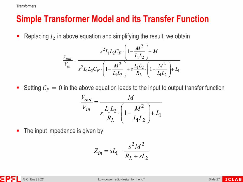
Simple Transformer Model and its Transfer Function
The transformer action gives
© C. Enz | 2021 Low-power radio design for the IoT Slide 26
1 1 2
1 2 2
in
out
V sL I sM IV sM I sL I
Finding 𝐼 from 1st equation and replacing in the 2nd equation leads to 2
22 1 2
inout M V sM IVIsL sL L
KCL at output node yields
2out
F in outL
VsC V V IR
Transformers
ICLAB
Simple Transformer Model and its Transfer Function Replacing 𝐼 in above equation and simplifying the result, we obtain
© C. Enz | 2021 Low-power radio design for the IoT Slide 27
221 2
1 22 2
2 1 21 2 1
1 2 1 2
1
1 1
Fout
inF
L
Ms L L C ML LV
V L LM Ms L L C s LL L R L L
Setting 𝐶 0 in the above equation leads to the input to output transfer function
21 2
11 2
1
out
in
L
V MV L L Ms L
R L L
The input impedance is given by
2 2
12
inL
s MZ sLR sL

Transformers
ICLAB
Stacked Transformers
Higher magnetic coupling
Unlike planar structures, primary and secondary can be identical and symmetrical
Overall area is less than planar structure
Larger capacitive coupling compared to planar structure
© C. Enz | 2021 Low-power radio design for the IoT Slide 28
One to one Stack transformer
One to two Stack transformer
Staggering of turns to reduce capacitive coupling

ICLAB
Outline Introduction
Inductors
Transformers
Varactors
© C. Enz | 2021 Low-power radio design for the IoT Slide 29
Varactors
ICLAB
Varactors Varactor is a voltage-dependent capacitor
Two important attributes of varactor design become critical in oscillator design The capacitance range i.e. ratio of maximum to minimum capacitance that varactor can
provide The quality factor of the varactor
© C. Enz | 2021 Low-power radio design for the IoT Slide 30
Varactors
ICLAB
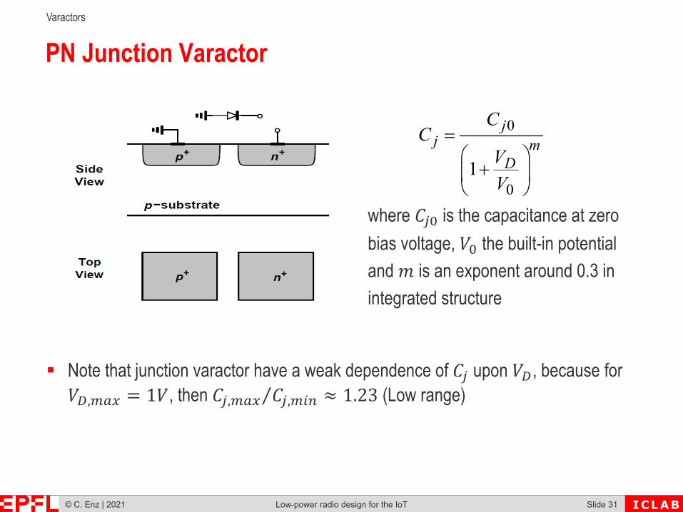
PN Junction Varactor
Note that junction varactor have a weak dependence of 𝐶 upon 𝑉 , because for 𝑉 , 1𝑉, then 𝐶 , 𝐶 ,⁄ 1.23 (Low range)
© C. Enz | 2021 Low-power radio design for the IoT Slide 31
0
01
jj m
D
CC
VV
where 𝐶 is the capacitance at zero bias voltage, 𝑉 the built-in potential and 𝑚 is an exponent around 0.3 in integrated structure

Varactors
ICLAB
Varactor Q Calculation Issues
As shown above, due to the two dimensional flow of current it is difficult to compute the equivalent series resistance of the structure
N-well sheet resistance can not be directly applied to calculation of varactor series resistance
© C. Enz | 2021 Low-power radio design for the IoT Slide 32
Current distribution in varactor
Q of varactor is obtained by measurement on fabricated structuresDifficult to calculate it because of the 2D current distribution

Varactors
ICLAB
MOS Varactor
A regular MOSFET exhibits a voltage dependent gate capacitance
The non-monotonic behavior with respect to gate voltage limits the design flexibility
© C. Enz | 2021 Low-power radio design for the IoT Slide 33
Variation of gate capacitance with 𝑉 for a regular MOS device
Varactors
ICLAB
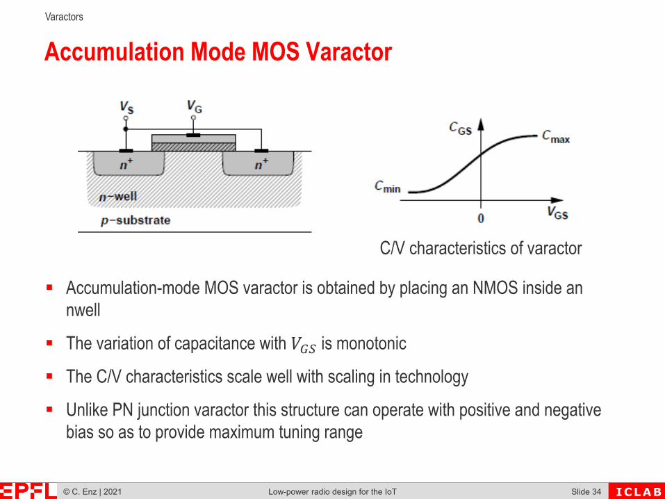
Accumulation Mode MOS Varactor
Accumulation-mode MOS varactor is obtained by placing an NMOS inside an nwell
The variation of capacitance with 𝑉 is monotonic
The C/V characteristics scale well with scaling in technology
Unlike PN junction varactor this structure can operate with positive and negative bias so as to provide maximum tuning range
© C. Enz | 2021 Low-power radio design for the IoT Slide 34
C/V characteristics of varactor

Varactors
ICLAB
Accumulation Mode MOS Varactor Operation
𝑉 𝑉
Depletion region is formed under gate oxide
Equivalent capacitance is the series combination of gate capacitance and depletion capacitance
𝑉 𝑉
Formation of channel under gate oxide
© C. Enz | 2021 Low-power radio design for the IoT Slide 35

Varactors
ICLAB
Q of Accumulation mode MOS Varactor
The Q of the varactor is determined by the resistance between source and drain terminals
Approximately calculated by lumped model shown in above
© C. Enz | 2021 Low-power radio design for the IoT Slide 36
Varactors
ICLAB
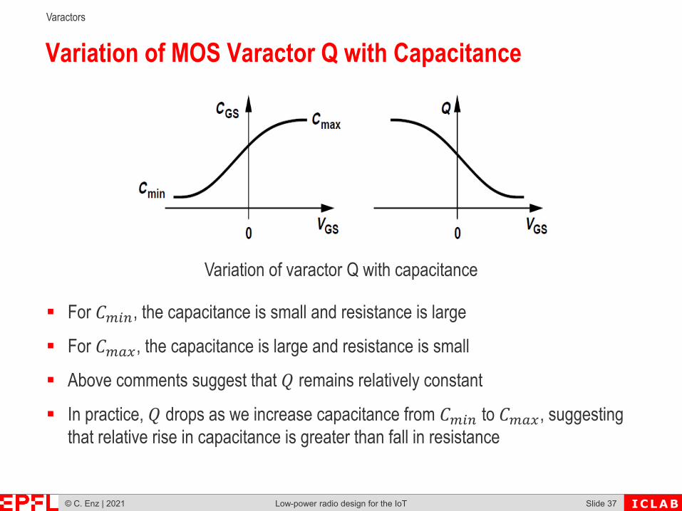
Variation of MOS Varactor Q with Capacitance
For 𝐶 , the capacitance is small and resistance is large
For 𝐶 , the capacitance is large and resistance is small
Above comments suggest that 𝑄 remains relatively constant
In practice, 𝑄 drops as we increase capacitance from 𝐶 to 𝐶 , suggesting that relative rise in capacitance is greater than fall in resistance
© C. Enz | 2021 Low-power radio design for the IoT Slide 37
Variation of varactor Q with capacitance
Varactors
ICLAB
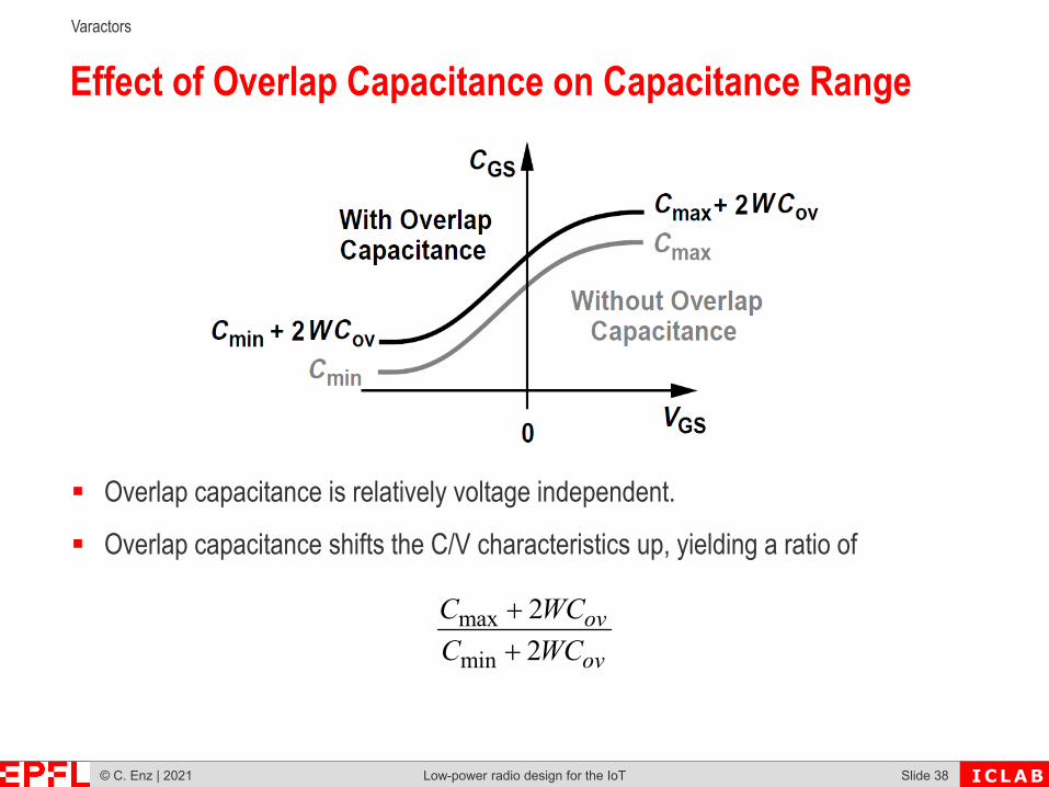
Effect of Overlap Capacitance on Capacitance Range
Overlap capacitance is relatively voltage independent.
Overlap capacitance shifts the C/V characteristics up, yielding a ratio of
© C. Enz | 2021 Low-power radio design for the IoT Slide 38
max
min
22
ov
ov
C WCC WC

ICLAB
ReferencesMost of this Chapter is based on Chapter 7 of Reference [1]
[1] B. Razavi, RF Microelectronics, 2nd ed. Pearson, 2012.
© C. Enz | 2021 Low-power radio design for the IoT Slide 39