Embed Size (px)
Citation preview

Integrated Passives for High-Frequency Applications 249
Integrated Passives for High-Frequency Applications
Xiaoyu Mi and Satoshi Ueda
x
Integrated Passives for High-Frequency Applications
Xiaoyu Mi and Satoshi Ueda
Fujitsu Laboratories Ltd. Japan
1. Introduction
1.1 Definitions of Integrated Passives Passive elements are indispensable in RF systems and are used for matching networks, LC tank circuits, attenuators, filtering, decoupling purposes and so on (Tilmans H. A C et al., 2003). Passive elements can be simply classified into distributed elements including transmission lines and waveguides, and lumped elements including inductors, capacitors and resistors. The distributed circuits take into account the phase shift occurring when the signal wave propagates along the circuits. As the operating frequency moves into the microwave spectrum, the distributed circuits have a higher Q factor, and thus they are usually used for high-frequency applications. Lumped elements are zero-dimensional by definition. In other words, the lumped elements have no physical dimensions which are significant with respect to the wavelength at the operating frequency, so that the phase shift that arises can be ignored. Discrete lumped elements are conventionally used in electronic circuits that work at a lower frequency. This is because the sizes of the discrete lumped elements become comparable to the wavelength at microwave frequencies. With the advent of new photolithography and passive integration technologies, the three basic building blocks for circuit design-inductors, capacitors, and resistors can be made small enough to be available in lumped form (Tummala R. R. et al., 2000). Lumped passive components may be discrete, integrated or embedded. The discrete is a singular device in a leaded or surface mount technology (SMT) case. This includes screen-printed resistors, capacitors, and inductors. Passive integration technologies allow several passive components to be integrated, either into a substrate (embedded) or onto a substrate (integrated). Integrated passive devices usually come in a compact SMT package or chip-scale package (CSP) as a stand-alone component with input, output and ground terminations, which is much smaller than the operating wavelength providing some complete circuit functions, such as impedance-matching, filtering and so on, for high-frequency applications up to several tens of GHz (Tilmans H. A C et al., 2003). The lumped element circuits have the advantage of a smaller size, lower cost, and wide-band characteristics, though the Q factor is generally lower than distributed circuits. Integrated lumped passive circuits with a small form factor are especially suitable for some RF and microwave applications where real estate or wide-band requirements are of prime importance, for example mobile phones or other handheld wireless products. The choice
13
www.intechopen.com

Advanced Microwave Circuits and Systems250
between lumped and distributed element depends on the circuit functions to be fulfilled, operating frequency, size and cost requirements, and performance targets. Sometime these factors must be considered generally before making a trade off between performance and cost or size. Lumped elements can be integrated together with distributed circuits to construct so-called half-lumped circuits enabling more flexible and complex circuit designs. The lumped-element circuits can also be integrated or combined (attached) with microwave integrated circuits (MICs) to construct RF modules (Bahl I. & Bhartia P., 2003). Embedded passives are buried into the substrate itself as an integral part of the substrate along with multiple layers of conductors and do not need to be mounted or connected to the substrate. The multiple inner layers of conductors are separated by a dielectric material with local metal vias to provide interconnects among these embedded passives. Ceramic substrates or printed circuit boards (PCBs) are used as the embedded substrates, since it is easy to build multiple interconnects inside these substrate. This chapter will focus on integration technologies for passive elements. The integration technologies can be classified into three categories according to the construction method used: ・ Laminate-based passive integration technology ・ LTCC (low-temperature-co-fired-ceramics) based passive integration technology ・ Thin-film-based passive integration technology Laminate-based technology and LTCC-based technology are technologies that allow the passive elements to be embedded or built in the LTCC or polymer substrate. In contrast, the thin-film-based technology is used to integrate passive circuits on the surface of a substrate by performing thin-film deposition of multiple layers of metals and dielectrics. Section 2 will give a comparison of the configuration and performance of these three technological approaches, from the viewpoints of microwave and milli-metre wave applications, and system miniaturization.
1.2 Reasons and Applications for Integrating Passive Devices Recently, there has been an explosion of growth in the wireless telecom industry. There is a strong market-driven demand to increase the functionality of internal electronics while drastically reducing the total size and cost, particularly in mobile radio frequency applications. This demand has been satisfied to date by major advances in integrated circuits and continuing reductions in the size of discrete surface-mounted passive components. The continuing reduction in the size of surface-mounted passive components is reaching its limit and producing diminishing returns because of the incompatibility of printed circuit board (PCB) technology as well as the high cost of assembly for those tiny discrete components. Nowadays, the 0603 or 0402 size surface-mounted devices are commonly used for printed circuit boards. The assembly cost usually includes the price of the discrete components and the conversion cost consisting of the cost of placement, soldering, and inspection. The typical conversion cost for installing one piece of 0603 or 0402 size SMD (surface-mounted devices) component is $0.02 which is typically more than the price of the SMD itself. SMD components smaller than 0402 will have a significant higher installation cost compared to the 0603 or 0420 size. Therefore further reductions in size and cost will come from integrating the passive components to reduce the component count. A typical mobile phone has hundreds of passive components and only 20 to 40 ICs. The discrete passive components account for 90% of the component count, 80% of the size and 70% of the cost in a handset. As mobile phones come with an increasing array of functions, their active component count
will likely remain stable. Therefore, the designers of compact electronics systems, especially handheld and wireless devices, who are being faced with more and more stringent board space constraints, are looking for alternative technologies to integrate these passive components into devices or to remove these passives from the PCB surface (Dougherty J. P. et al., 2003; Doyle L., 2005). Functional integration (system integration) is another key to miniaturizing handsets. RF modules are moving to higher levels of integration. The modules are required to offer more functionality and higher performance, incorporate the passive circuit inside, and occupy a smaller footprint (Norlyng S., 2003; Pulsford N., 2002). Despite many years of research, the IC industry is facing a technological barrier preventing the integration of bulky, expensive, off-chip passive RF components, such as high-Q inductors, capacitors, varactor diodes and ceramic filters. These components are limiting reduction in size. On-chip passive components, fabricated along with the active elements, as part of the semiconductor wafer in various RFIC technologies have failed to provide adequately high-quality factors compared to the off-chip passives. The typical Q factor of an integrated inductor using (Bi) CMOS or bipolar technologies is usually around 10 (Tilmans H. A C et al., 2003). It can be increased up to between 20 and 30 by introducing some special processing steps that are usually complex and costly, such as etching away the Si under the inductors (Jiang H. et al., 2000) or placing a very thick insulation layer between the inductor and the Si wafer (Kim D. et al., 2003). However, these processes are still not enough for the many important circuit functions in wireless communications systems. For RF front end and radio transceiver applications, it is preferable for the inductor to have a Q factor of at least 30. System-in-package solutions (SIP) are promising as a means of combining these passives and actives together in a single package. The SIP solutions require the passives be small and easy to combine with other devices. The evolution of module technology strongly depends on improvements in passive integration and 3D assembly technologies. Moreover, the continuing scaling of IC technology affects the required interconnection and packaging technologies significantly. Improvements in the density of standard interconnection and packaging technologies have not kept pace with IC scaling trends, resulting in a so-called “interconnect technology gap” (Wojnowski M. et al., 2008). The peripheral pads pitch of IC will trend to less than 30 μm in the near future. In contrast, standard PCB technology commonly provides a coarse contact pitch of 400-1000 μm. An interposer enabling high-density interconnection has to be used between the high-density IC technology and the coarse standard PCB technology. The future MCM (Multi-Chip-Module) substrates and packages are required to function as so-called interposers. To incorporate the passive circuit into the interposer is attractive and powerful for constructing next-generation SIP modules (Carchon G. et al, 2008). Over the past 10 years, passive integration technology has gone through a significant evolution to meet the requirements for lower cost solutions, system miniaturization, and high levels of functionality integration, improved reliability, and high-volume applications. In addition, the passive integration technologies have been leading to the benefits show below: ・ Smaller size, weight, and volume ・ Improved electrical performance due to the proximity of the passives to the active
devices reducing parasitic and increasing switching speeds ・ Improved reliability through a reduction in the number of solder connections
www.intechopen.com

Integrated Passives for High-Frequency Applications 251
between lumped and distributed element depends on the circuit functions to be fulfilled, operating frequency, size and cost requirements, and performance targets. Sometime these factors must be considered generally before making a trade off between performance and cost or size. Lumped elements can be integrated together with distributed circuits to construct so-called half-lumped circuits enabling more flexible and complex circuit designs. The lumped-element circuits can also be integrated or combined (attached) with microwave integrated circuits (MICs) to construct RF modules (Bahl I. & Bhartia P., 2003). Embedded passives are buried into the substrate itself as an integral part of the substrate along with multiple layers of conductors and do not need to be mounted or connected to the substrate. The multiple inner layers of conductors are separated by a dielectric material with local metal vias to provide interconnects among these embedded passives. Ceramic substrates or printed circuit boards (PCBs) are used as the embedded substrates, since it is easy to build multiple interconnects inside these substrate. This chapter will focus on integration technologies for passive elements. The integration technologies can be classified into three categories according to the construction method used: ・ Laminate-based passive integration technology ・ LTCC (low-temperature-co-fired-ceramics) based passive integration technology ・ Thin-film-based passive integration technology Laminate-based technology and LTCC-based technology are technologies that allow the passive elements to be embedded or built in the LTCC or polymer substrate. In contrast, the thin-film-based technology is used to integrate passive circuits on the surface of a substrate by performing thin-film deposition of multiple layers of metals and dielectrics. Section 2 will give a comparison of the configuration and performance of these three technological approaches, from the viewpoints of microwave and milli-metre wave applications, and system miniaturization.
1.2 Reasons and Applications for Integrating Passive Devices Recently, there has been an explosion of growth in the wireless telecom industry. There is a strong market-driven demand to increase the functionality of internal electronics while drastically reducing the total size and cost, particularly in mobile radio frequency applications. This demand has been satisfied to date by major advances in integrated circuits and continuing reductions in the size of discrete surface-mounted passive components. The continuing reduction in the size of surface-mounted passive components is reaching its limit and producing diminishing returns because of the incompatibility of printed circuit board (PCB) technology as well as the high cost of assembly for those tiny discrete components. Nowadays, the 0603 or 0402 size surface-mounted devices are commonly used for printed circuit boards. The assembly cost usually includes the price of the discrete components and the conversion cost consisting of the cost of placement, soldering, and inspection. The typical conversion cost for installing one piece of 0603 or 0402 size SMD (surface-mounted devices) component is $0.02 which is typically more than the price of the SMD itself. SMD components smaller than 0402 will have a significant higher installation cost compared to the 0603 or 0420 size. Therefore further reductions in size and cost will come from integrating the passive components to reduce the component count. A typical mobile phone has hundreds of passive components and only 20 to 40 ICs. The discrete passive components account for 90% of the component count, 80% of the size and 70% of the cost in a handset. As mobile phones come with an increasing array of functions, their active component count
will likely remain stable. Therefore, the designers of compact electronics systems, especially handheld and wireless devices, who are being faced with more and more stringent board space constraints, are looking for alternative technologies to integrate these passive components into devices or to remove these passives from the PCB surface (Dougherty J. P. et al., 2003; Doyle L., 2005). Functional integration (system integration) is another key to miniaturizing handsets. RF modules are moving to higher levels of integration. The modules are required to offer more functionality and higher performance, incorporate the passive circuit inside, and occupy a smaller footprint (Norlyng S., 2003; Pulsford N., 2002). Despite many years of research, the IC industry is facing a technological barrier preventing the integration of bulky, expensive, off-chip passive RF components, such as high-Q inductors, capacitors, varactor diodes and ceramic filters. These components are limiting reduction in size. On-chip passive components, fabricated along with the active elements, as part of the semiconductor wafer in various RFIC technologies have failed to provide adequately high-quality factors compared to the off-chip passives. The typical Q factor of an integrated inductor using (Bi) CMOS or bipolar technologies is usually around 10 (Tilmans H. A C et al., 2003). It can be increased up to between 20 and 30 by introducing some special processing steps that are usually complex and costly, such as etching away the Si under the inductors (Jiang H. et al., 2000) or placing a very thick insulation layer between the inductor and the Si wafer (Kim D. et al., 2003). However, these processes are still not enough for the many important circuit functions in wireless communications systems. For RF front end and radio transceiver applications, it is preferable for the inductor to have a Q factor of at least 30. System-in-package solutions (SIP) are promising as a means of combining these passives and actives together in a single package. The SIP solutions require the passives be small and easy to combine with other devices. The evolution of module technology strongly depends on improvements in passive integration and 3D assembly technologies. Moreover, the continuing scaling of IC technology affects the required interconnection and packaging technologies significantly. Improvements in the density of standard interconnection and packaging technologies have not kept pace with IC scaling trends, resulting in a so-called “interconnect technology gap” (Wojnowski M. et al., 2008). The peripheral pads pitch of IC will trend to less than 30 μm in the near future. In contrast, standard PCB technology commonly provides a coarse contact pitch of 400-1000 μm. An interposer enabling high-density interconnection has to be used between the high-density IC technology and the coarse standard PCB technology. The future MCM (Multi-Chip-Module) substrates and packages are required to function as so-called interposers. To incorporate the passive circuit into the interposer is attractive and powerful for constructing next-generation SIP modules (Carchon G. et al, 2008). Over the past 10 years, passive integration technology has gone through a significant evolution to meet the requirements for lower cost solutions, system miniaturization, and high levels of functionality integration, improved reliability, and high-volume applications. In addition, the passive integration technologies have been leading to the benefits show below: ・ Smaller size, weight, and volume ・ Improved electrical performance due to the proximity of the passives to the active
devices reducing parasitic and increasing switching speeds ・ Improved reliability through a reduction in the number of solder connections
www.intechopen.com

Advanced Microwave Circuits and Systems252
・ Lower total cost due to reduced costs for procurement, logistics and installation Passive integration technologies can be used in both digital and analog/RF applications. Some of these applications include mobile phones, personal digital assistants (PDAs), wireless computer networks, radar systems, and phased array antennas. Integrated passive circuits with high-performance characteristics function in these systems as: ・ RF front end modules ・ RF power amplifier couplers ・ Filters (low pass, high pass and band pass) ・ Functional interposers between ICs and the primary interconnect substrate ・ Multi-band transceivers
1.3 General Design Considerations for Integrated Passives Inductor One of the most critical elements in RF and microwave circuits for high-frequency wireless applications is the inductor. If the Q value is too low, the lumped circuit will not reach the desired performance targets. Spiral inductors providing a high Q factor and inductance value are commonly used for high-density circuits. The important characteristics of an inductor are its inductance value and its parasitic capacitance and resistance, which determine its Q factor and self-resonant frequency. The Q factor values can be obtained from one-port or two-port scattering parameter data. A simplified one-port lumped-element equivalent circuit model used to characterize inductors is shown in Fig. 1.1. Accurate inductor models using measured two-port scattering parameters will be discussed in section 3. In this one-port model, L, R, and C represent the total inductance, series resistance, and parasitic capacitance of the inductor, respectively. The admittance of an inductor is expressed as
LjRCjY 1
)( 222222 LRLCj
LRR
. (1.1)
The series resistance R used to model the dissipative loss is given by
fRfRRR dacdc (1.2) where dcR represents DC resistance of the inductor, acR models resistance due to skin
effect in the conductive trace, and dR represents resistance due to eddy current excitation and dielectric loss in the substrate. The Y parameters can be obtained from one-port S parameter. The Q factor is then calculated from
YYQ ReIm . (1.3)
Fig.1.1 Simplified one-port lumped-element equivalent circuit model of an inductor When the parasitic capacitance C is very small and ignorable, Q factor can be given by
RLQ . (1.4)
As can be seen in the above-mentioned equation (1.4), achieving a predetermined inductance L at a small resistance R contributes to an increase in the Q-factor. The self-resonant frequency (SRF) of an inductor is determined by the Y parameter when
0)Im( Y , that is to say,
0220
20
0 LR
LC . (1.5)
Using the self-resonance condition, equation (1.5), the self-resonant frequency of is then given by the following equation.
2
2121
LR
LCfo . (1.6)
Usually the R is small, so self-resonant frequency of can be estimated by
LCfo
121 . (1.7)
When self-resonance occurs, the inductive reactance and the parasitic capacitive reactance become equal. Beyond the self-resonant frequency, the inductor becomes capacitive. The self-resonant frequency decides the frequency from which the inductor cannot work well as an inductor any more. The self-resonant frequency of an inductor is supposed to be much higher than its operating frequency. To increase the self-resonant frequency, the parasitic capacitance C in an inductor has to be suppressed. The maximum diameter of an inductor should be less than 30/ in order to avoid distributed effects. High-frequency applications require a smaller size and higher self-
www.intechopen.com

Integrated Passives for High-Frequency Applications 253
・ Lower total cost due to reduced costs for procurement, logistics and installation Passive integration technologies can be used in both digital and analog/RF applications. Some of these applications include mobile phones, personal digital assistants (PDAs), wireless computer networks, radar systems, and phased array antennas. Integrated passive circuits with high-performance characteristics function in these systems as: ・ RF front end modules ・ RF power amplifier couplers ・ Filters (low pass, high pass and band pass) ・ Functional interposers between ICs and the primary interconnect substrate ・ Multi-band transceivers
1.3 General Design Considerations for Integrated Passives Inductor One of the most critical elements in RF and microwave circuits for high-frequency wireless applications is the inductor. If the Q value is too low, the lumped circuit will not reach the desired performance targets. Spiral inductors providing a high Q factor and inductance value are commonly used for high-density circuits. The important characteristics of an inductor are its inductance value and its parasitic capacitance and resistance, which determine its Q factor and self-resonant frequency. The Q factor values can be obtained from one-port or two-port scattering parameter data. A simplified one-port lumped-element equivalent circuit model used to characterize inductors is shown in Fig. 1.1. Accurate inductor models using measured two-port scattering parameters will be discussed in section 3. In this one-port model, L, R, and C represent the total inductance, series resistance, and parasitic capacitance of the inductor, respectively. The admittance of an inductor is expressed as
LjRCjY 1
)( 222222 LRLCj
LRR
. (1.1)
The series resistance R used to model the dissipative loss is given by
fRfRRR dacdc (1.2) where dcR represents DC resistance of the inductor, acR models resistance due to skin
effect in the conductive trace, and dR represents resistance due to eddy current excitation and dielectric loss in the substrate. The Y parameters can be obtained from one-port S parameter. The Q factor is then calculated from
YYQ ReIm . (1.3)
Fig.1.1 Simplified one-port lumped-element equivalent circuit model of an inductor When the parasitic capacitance C is very small and ignorable, Q factor can be given by
RLQ . (1.4)
As can be seen in the above-mentioned equation (1.4), achieving a predetermined inductance L at a small resistance R contributes to an increase in the Q-factor. The self-resonant frequency (SRF) of an inductor is determined by the Y parameter when
0)Im( Y , that is to say,
0220
20
0 LR
LC . (1.5)
Using the self-resonance condition, equation (1.5), the self-resonant frequency of is then given by the following equation.
2
2121
LR
LCfo . (1.6)
Usually the R is small, so self-resonant frequency of can be estimated by
LCfo
121 . (1.7)
When self-resonance occurs, the inductive reactance and the parasitic capacitive reactance become equal. Beyond the self-resonant frequency, the inductor becomes capacitive. The self-resonant frequency decides the frequency from which the inductor cannot work well as an inductor any more. The self-resonant frequency of an inductor is supposed to be much higher than its operating frequency. To increase the self-resonant frequency, the parasitic capacitance C in an inductor has to be suppressed. The maximum diameter of an inductor should be less than 30/ in order to avoid distributed effects. High-frequency applications require a smaller size and higher self-
www.intechopen.com

Advanced Microwave Circuits and Systems254
resonant frequency, so the inductance density also becomes more and more important. Therefore a major design goal for inductor components is to increase the Q factor, density of inductors and self-resonant frequency. Capacitor There are two types of passive capacitors generally used in RF and microwave circuits: interdigital, and metal-insulator-metal (MIM). The choice between the interdigital and MIM capacitors mainly depends on the capacitance value to be made. Usually interdigital capacitors are only used to realize capacitance values less than 1 pF. For capacitance values greater than 1 pF, MIM structures are generally used to minimize the overall size and to avoid the distributed effects. For a capacitance value greater than 200 pF, usually surface-mounted devices are necessary. The capacitor performance is strongly associated with the Q-factor and parasitic inductance of the capacitor. The parasitic inductance L caused by the connection to the capacitor electrodes must be accounted for. The effective capacitance eC is given by
20
2
1ffCCe (1.8)
where LC
fo1
21 is the self-resonant frequency of the capacitor and f is the
operating frequency. When the capacitor operates at the self-resonant frequency, the capacitance will become zero. To have effective capacitance reach the designed capacitance C, the parasitic inductance in the capacitor has to be suppressed. The quality factor of MIM capacitors is given by
dc
dc
dcQQQQ
QQQ 11
1. (1.9)
Where CRQc /1 accounting for conducting loss resulted from the wiring and
electrode resistor R, and tan/1dQ accounting for dielectric loss in the capacitor.
tan is the loss tangent of the insulator material of the capacitor. To achieve a high Q-factor, it is essential to reduce the conducting loss in the wiring and electrode and to use dielectric material with a small loss tangent. The dimension of capacitors should be less than 0.1 λ in dielectric film high-frequency applications. To increase high-frequency performance and the passive circuit density and reduce the cost, a large capacitance density is highly desirable. Silicon oxide and nitride are commonly used in conventional MIM capacitors. They can provide good voltage linearity and low-temperature coefficients. Their capacitance density will be limited by their low dielectric permittivity. The capacitance density can be given by dtk /0 . Attempts to
increase the capacitance density by reducing the dielectric thickness ( dt ) usually cause an undesired high leakage current and poor loss tangent. Therefore, high-k dielectric materials are necessary to provide good electrical performances and increase the circuit density.
Resistor Integrated resistors can be produced either by depositing a thin film of lossy metal on a dielectric substrate or by screen-printing a resistive paste to form a thick-film resistor on or in a ceramics or PCB substrate. Nichrome and tantalum nitride are the most popular film materials for thin-film resistors. SiCr and poly-silicon thin films also used for thin-film resistors. TaN is preferred to NiCr for RF applications, due to the presence of undesirable magnetic material, i.e., nickel, in NiCr, which is believed to introduce unwanted inter-modulation products in multi-carrier wireless systems. Ruthenium dioxide paste and carbon-filled polymer paste are widely used for thick-film resistors. A common problem with planar film resistors is the parasitic capacitance arising form the underlying dielectric region and the distributed inductance. These parasitics make the resistors have a frequency dependence at high frequencies. To shorten the resistor length by introducing films having a larger sheet resistivity is helpful for suppressing the parasitics. Desirable characteristics of resistors for high-frequency applications are summarized below. ・ Stable resistance value without changing with time ・ Low temperature coefficient of resistance (TCR) ・ Large sheet resistivity (kΩ/square to MΩ/square) to minimize the parasitics and to
guarantee the resistor length less than 0.1 λ so that distribution effects can be ignored ・ Adequate power dissipation capability The required tolerances for passive components are roughly summarized in Table 1-1. Analog and RF applications typically necessitate small tolerances of less than±5% and high-performance characteristics such as high Q factors and high self-resonance frequency.
Application Element Type Required Tolerance Damping Resistor (10-33Ω) ±30% Bypass Capacitor (50 pF-1 μF) ±30% Pull-up, Pull-down Resistor (500-1 MΩ) ±10% Integral calculus circuit Capacitor (100 pF-1 μF) ±15% Differential circuit Capacitor (10 pF-10 μF) ±5% Oscillation circuit Capacitor (10 pF-10 μF) ±5% Bias circuit Resistor(1 k-10 MΩ) ±1% IC controlling Resistor(≧10 kΩ) ±1% Filter Capacitor(≦1 μF);
Inductor(≦100 nH) ±5%
Impedance matching Resistor(50-100 Ω); Capacitor(≦10 nF)& Inductor(≦100 nH)
±5%
Table 1.1 Required tolerances for passive components
2. Current Research Status and Trend of Passive Integration
2.1 Laminate-Based Passive Integration Technology Laminate-based passive integration technology is extended from printed circuit board (PCB) technology which has been extensively used for all electronic applications. The primary
www.intechopen.com

Integrated Passives for High-Frequency Applications 255
resonant frequency, so the inductance density also becomes more and more important. Therefore a major design goal for inductor components is to increase the Q factor, density of inductors and self-resonant frequency. Capacitor There are two types of passive capacitors generally used in RF and microwave circuits: interdigital, and metal-insulator-metal (MIM). The choice between the interdigital and MIM capacitors mainly depends on the capacitance value to be made. Usually interdigital capacitors are only used to realize capacitance values less than 1 pF. For capacitance values greater than 1 pF, MIM structures are generally used to minimize the overall size and to avoid the distributed effects. For a capacitance value greater than 200 pF, usually surface-mounted devices are necessary. The capacitor performance is strongly associated with the Q-factor and parasitic inductance of the capacitor. The parasitic inductance L caused by the connection to the capacitor electrodes must be accounted for. The effective capacitance eC is given by
20
2
1ffCCe (1.8)
where LC
fo1
21 is the self-resonant frequency of the capacitor and f is the
operating frequency. When the capacitor operates at the self-resonant frequency, the capacitance will become zero. To have effective capacitance reach the designed capacitance C, the parasitic inductance in the capacitor has to be suppressed. The quality factor of MIM capacitors is given by
dc
dc
dcQQQQ
QQQ 11
1. (1.9)
Where CRQc /1 accounting for conducting loss resulted from the wiring and
electrode resistor R, and tan/1dQ accounting for dielectric loss in the capacitor.
tan is the loss tangent of the insulator material of the capacitor. To achieve a high Q-factor, it is essential to reduce the conducting loss in the wiring and electrode and to use dielectric material with a small loss tangent. The dimension of capacitors should be less than 0.1 λ in dielectric film high-frequency applications. To increase high-frequency performance and the passive circuit density and reduce the cost, a large capacitance density is highly desirable. Silicon oxide and nitride are commonly used in conventional MIM capacitors. They can provide good voltage linearity and low-temperature coefficients. Their capacitance density will be limited by their low dielectric permittivity. The capacitance density can be given by dtk /0 . Attempts to
increase the capacitance density by reducing the dielectric thickness ( dt ) usually cause an undesired high leakage current and poor loss tangent. Therefore, high-k dielectric materials are necessary to provide good electrical performances and increase the circuit density.
Resistor Integrated resistors can be produced either by depositing a thin film of lossy metal on a dielectric substrate or by screen-printing a resistive paste to form a thick-film resistor on or in a ceramics or PCB substrate. Nichrome and tantalum nitride are the most popular film materials for thin-film resistors. SiCr and poly-silicon thin films also used for thin-film resistors. TaN is preferred to NiCr for RF applications, due to the presence of undesirable magnetic material, i.e., nickel, in NiCr, which is believed to introduce unwanted inter-modulation products in multi-carrier wireless systems. Ruthenium dioxide paste and carbon-filled polymer paste are widely used for thick-film resistors. A common problem with planar film resistors is the parasitic capacitance arising form the underlying dielectric region and the distributed inductance. These parasitics make the resistors have a frequency dependence at high frequencies. To shorten the resistor length by introducing films having a larger sheet resistivity is helpful for suppressing the parasitics. Desirable characteristics of resistors for high-frequency applications are summarized below. ・ Stable resistance value without changing with time ・ Low temperature coefficient of resistance (TCR) ・ Large sheet resistivity (kΩ/square to MΩ/square) to minimize the parasitics and to
guarantee the resistor length less than 0.1 λ so that distribution effects can be ignored ・ Adequate power dissipation capability The required tolerances for passive components are roughly summarized in Table 1-1. Analog and RF applications typically necessitate small tolerances of less than±5% and high-performance characteristics such as high Q factors and high self-resonance frequency.
Application Element Type Required Tolerance Damping Resistor (10-33Ω) ±30% Bypass Capacitor (50 pF-1 μF) ±30% Pull-up, Pull-down Resistor (500-1 MΩ) ±10% Integral calculus circuit Capacitor (100 pF-1 μF) ±15% Differential circuit Capacitor (10 pF-10 μF) ±5% Oscillation circuit Capacitor (10 pF-10 μF) ±5% Bias circuit Resistor(1 k-10 MΩ) ±1% IC controlling Resistor(≧10 kΩ) ±1% Filter Capacitor(≦1 μF);
Inductor(≦100 nH) ±5%
Impedance matching Resistor(50-100 Ω); Capacitor(≦10 nF)& Inductor(≦100 nH)
±5%
Table 1.1 Required tolerances for passive components
2. Current Research Status and Trend of Passive Integration
2.1 Laminate-Based Passive Integration Technology Laminate-based passive integration technology is extended from printed circuit board (PCB) technology which has been extensively used for all electronic applications. The primary
www.intechopen.com

Advanced Microwave Circuits and Systems256
function of conventional PCBs is to provide mechanical carrier and multilevel electrical interconnections for packaged solid state devices and passive components. Embedded passive technologies on organic substrates were introduced by Packaging Research Centre, Georgia Institute of Technology in 1993. Since then several embedded passive technologies have been developed (Dougherty J. P. et al., 2003; Jung E. et al., 2009; Chason M. et al., 2006). System integration based on embedded passive in PCBs is illustrated in Fig. 1.2 (a) and (b). The embedded substrate is constructed by laminating together polymer-based dielectric or resistive films on which metal conductor are defined on one or both sides. The discrete components can also be buried into the organic substrate for process simplicity. Recently, some advanced PCB technologies have offered embedded passives for low-GHz RF applications, such as a Bluetooth transceiver module, power amplifier module or sensors (Li L. et al., 2003; Li L. et al., 2004; Vatanparast R. et al., 2007).
Embedded Discrete Passives Technology The simplest embedded passive solution is to embed discrete SMT components into a multilayer organic substrate. The SMT passives are buried in the individual layers that usually are the core-layer (Sugaya Y. et al., 2001; Wu S. M. et al., 2007). On one or both sides of the core-layer, the build-up layers are laminated and vias are formed to provide interconnections for the embedded SMT passives (Shibasaki S. et al., 2004). This solution uses SMD components and offers a relatively simple fabrication process and high reliability and accuracy. For example, SMD film resistors can be made with inter-metallic semi- amorphous alloys with a low thermal coefficient of resistance. The resistance can be laser-trimmed to within 0.1 % accuracy. SMD inductors are optimized according to value and
(a)
(b) Fig.2.1 System integration based on embedded passive in PCB. (a) Embedded Discrete Passives Technology; (b) Embedded Film Passives Technology
performance with thin-film, thick-film or wire wound technology. With high-tolerance SMD capacitors, components can be selected in terms of which capacitors to embed, and this can lead to improved final capacitance accuracy. An embedded substrate using a discrete SMD is usually thick and big compared to film elements due to the large size of the buried SMD components. To embed SMD components contradicts the minimization purpose to some extent. Several companies have checked the reliabilities of this solution and have used it for mass production (Shibasaki S. et al., 2004; Kamiya H. et al., 2005; Kondou K. & Kamimura R., 2002). Embedded Film Resistor Technology Three material technologies have been developed for embedded resistors: thin-film metal (such as NiP), thick-film ceramics, and polymer thick-film (PTF) materials. Their performance comparison is listed in Table 2.1. Copper foils supplied with a resistive thin-film coating are available (Ohmega Technologies, Inc.; Ticer Technologies; Norlyng S., 2003). The thin film metals typically comprise Ni, NiP, NiCr, or NiCrAlSi. These kinds of metal or metal alloy are deposited onto a copper foil by sputtering, evaporation, CVD or plating, depending on the required composition. The deposited thickness ranges from 50 nm to 400 nm. The resistive foils can be laminated onto a core layer. Then photolithography and etching are conducted to define the copper electrodes and to remove the unwanted resistive material. Highly accurate resistors necessitate a laser trimming process (Fjeldsted K., 2004). After resistors have been defined, the following multilayer processing steps like stacking and lamination can be conducted. Thin-film metals have a good TCR performance and are usually used to form small and accurate embedded resistors. Selective plating of NiP can also be used after the copper pattern is defined and etched (M-Pass, MacDermid Inc.). The plating time defines the thickness and resistivity. Due to the relative low sheet resistivity, this technology is not suited for high resistor values.
Table 2.1 Performance comparison of resistive film materials Polymer thick-film (PTF) materials can be screen-printed and cured at temperatures from 100 to 200℃ (Jillek, W. et al., 2005). The typical cured film thicknesses range form 15-20 μm. Aerosol-based deposition and Ink-jet printing for resistor-film formation were also reported (Hong T. K. & Kheng L. T., 2005; Shah V. G. & Hayes D. J., 2003). PTF materials are an attractive option and popularly used by the PCB industry due to their flexibility in sheet
Material Classes Thin-Film Metal Thick-Film Ceramics Polymer Thick-Film
Materials Ni-P; Doped Pt; Ni-Cr; Ni-Cr-Al-Si
Metal oxide powder + Glass powder
Carbon powder +
Polymer
Sheet resistance (Ω/square)
10-1 k 10-1 M 10-1 M
Tolerance ±5-10% ±10-20% ±15-20% TCR (ppm/℃) ±50-100 ±150-250 ±350 Formation Etching
or Plating Screen Printing Firing (500-900℃)
Screen Printing Heat hardening (≦200℃)
www.intechopen.com

Integrated Passives for High-Frequency Applications 257
function of conventional PCBs is to provide mechanical carrier and multilevel electrical interconnections for packaged solid state devices and passive components. Embedded passive technologies on organic substrates were introduced by Packaging Research Centre, Georgia Institute of Technology in 1993. Since then several embedded passive technologies have been developed (Dougherty J. P. et al., 2003; Jung E. et al., 2009; Chason M. et al., 2006). System integration based on embedded passive in PCBs is illustrated in Fig. 1.2 (a) and (b). The embedded substrate is constructed by laminating together polymer-based dielectric or resistive films on which metal conductor are defined on one or both sides. The discrete components can also be buried into the organic substrate for process simplicity. Recently, some advanced PCB technologies have offered embedded passives for low-GHz RF applications, such as a Bluetooth transceiver module, power amplifier module or sensors (Li L. et al., 2003; Li L. et al., 2004; Vatanparast R. et al., 2007).
Embedded Discrete Passives Technology The simplest embedded passive solution is to embed discrete SMT components into a multilayer organic substrate. The SMT passives are buried in the individual layers that usually are the core-layer (Sugaya Y. et al., 2001; Wu S. M. et al., 2007). On one or both sides of the core-layer, the build-up layers are laminated and vias are formed to provide interconnections for the embedded SMT passives (Shibasaki S. et al., 2004). This solution uses SMD components and offers a relatively simple fabrication process and high reliability and accuracy. For example, SMD film resistors can be made with inter-metallic semi- amorphous alloys with a low thermal coefficient of resistance. The resistance can be laser-trimmed to within 0.1 % accuracy. SMD inductors are optimized according to value and
(a)
(b) Fig.2.1 System integration based on embedded passive in PCB. (a) Embedded Discrete Passives Technology; (b) Embedded Film Passives Technology
performance with thin-film, thick-film or wire wound technology. With high-tolerance SMD capacitors, components can be selected in terms of which capacitors to embed, and this can lead to improved final capacitance accuracy. An embedded substrate using a discrete SMD is usually thick and big compared to film elements due to the large size of the buried SMD components. To embed SMD components contradicts the minimization purpose to some extent. Several companies have checked the reliabilities of this solution and have used it for mass production (Shibasaki S. et al., 2004; Kamiya H. et al., 2005; Kondou K. & Kamimura R., 2002). Embedded Film Resistor Technology Three material technologies have been developed for embedded resistors: thin-film metal (such as NiP), thick-film ceramics, and polymer thick-film (PTF) materials. Their performance comparison is listed in Table 2.1. Copper foils supplied with a resistive thin-film coating are available (Ohmega Technologies, Inc.; Ticer Technologies; Norlyng S., 2003). The thin film metals typically comprise Ni, NiP, NiCr, or NiCrAlSi. These kinds of metal or metal alloy are deposited onto a copper foil by sputtering, evaporation, CVD or plating, depending on the required composition. The deposited thickness ranges from 50 nm to 400 nm. The resistive foils can be laminated onto a core layer. Then photolithography and etching are conducted to define the copper electrodes and to remove the unwanted resistive material. Highly accurate resistors necessitate a laser trimming process (Fjeldsted K., 2004). After resistors have been defined, the following multilayer processing steps like stacking and lamination can be conducted. Thin-film metals have a good TCR performance and are usually used to form small and accurate embedded resistors. Selective plating of NiP can also be used after the copper pattern is defined and etched (M-Pass, MacDermid Inc.). The plating time defines the thickness and resistivity. Due to the relative low sheet resistivity, this technology is not suited for high resistor values.
Table 2.1 Performance comparison of resistive film materials Polymer thick-film (PTF) materials can be screen-printed and cured at temperatures from 100 to 200℃ (Jillek, W. et al., 2005). The typical cured film thicknesses range form 15-20 μm. Aerosol-based deposition and Ink-jet printing for resistor-film formation were also reported (Hong T. K. & Kheng L. T., 2005; Shah V. G. & Hayes D. J., 2003). PTF materials are an attractive option and popularly used by the PCB industry due to their flexibility in sheet
Material Classes Thin-Film Metal Thick-Film Ceramics Polymer Thick-Film
Materials Ni-P; Doped Pt; Ni-Cr; Ni-Cr-Al-Si
Metal oxide powder + Glass powder
Carbon powder +
Polymer
Sheet resistance (Ω/square)
10-1 k 10-1 M 10-1 M
Tolerance ±5-10% ±10-20% ±15-20% TCR (ppm/℃) ±50-100 ±150-250 ±350 Formation Etching
or Plating Screen Printing Firing (500-900℃)
Screen Printing Heat hardening (≦200℃)
www.intechopen.com

Advanced Microwave Circuits and Systems258
resistivity (10 Ω~1 MΩ/Square), the ability to print multiple sheet resistivity inks on one layer, and their low cost compared with thin-film metals and thick-film ceramics materials. The challenges of using PTF resistors have been accurate printing and finished resistor stability. Screen-printing is less precise in controlling dimensions than print-and-etch processes used for thin-film metals. Usually screen printing has a tolerance in the order of ±30 μm, whereas etching a PCB feature allows dimensional control in the order of about 10 μm. Additionally, the PTF resistors must be cured, and the resistivity of the finished materials exhibits dependence on the cure profile. Therefore, tolerances on PTF resistors are considered to be higher than those of the thin-film metals. Resistor stability is another concern when using PTF. PTF termination directly on copper results in a relatively poor resistor stability under environmental stress (exposure to 85% RH, 85℃) due to corrosion at the copper/carbon ink interface (Chason M. et al., 2006). Using immersion silver on etched copper pads as the corrosion barrier mitigates the resistor drift under environmental stress while preserving the precise dimensions of the photo-lithographically patterned copper (Savic J. et al., 2002; Dunn G. et al., 2004). PTF resistors are relatively poor in TCR compared to thin-film metal and thick-film ceramics materials. Thick-film ceramic resistive paste is usually used with copper foils. The pastes are screen printed on the copper foil and fired in an N2 atmosphere at a high temperature(500~900℃). Then the copper foil is laminated to a core layer or pre-preg. The conductor pattern is defined by photolithography and copper etching processes (Bauer W., 2003; Borland W. et al., 2002). A wide range of sheet resistance values are available with thick film ceramics pastes. Typical fired thicknesses range from 10 to 15 μm. Embedded Film Capacitor Technology Embedded film capacitors have restricted ranges of capacitance values based on the choice of dielectric material, capacitor structure and area allowed. Some popular dielectric materials used in embedded capacitors and their properties are listed in Table 2.2. The challenges for embedded film capacitors have been developing stable high-k materials and forming thin dielectric films. The modern PCB industry uses unloaded epoxy resin as An insulation layer between copper conductors. Typical unloaded epoxy resin has a relatively low dielectric constant (~4) and the resin thickness is approximately 50μm, resulting in a capacitance density of 0.7 pF/mm2, too small to embed typical capacitor values in a reasonable area. Many ceramic-filled resins, such as BaTiO3 in epoxy or Polyimide, have been developed for high-capacitance-density dielectrics (Ulrich R. & Schaper L. W., 2003). Non-photosensitive-type ceramic-filled resins usually come in laminate sheet form compatible with typical PCB fabrication techniques (Norlyng S., 2003; Oak-Mitsui Technologies Technical Data; 3M C-ply Technical Data; Kumashiro Y. et al., 2004). The non-photosensitive-type ceramic-filled resin is coated on a copper foil and after curing the ceramic-filled resin film, another piece of copper foil is stuck to the other side of the ceramic-filled resin film. The electrodes of film capacitors are formed by a photolithography process and the copper foils are etched on ether one side or both sides of an insulator film. Non-photosensitive type ceramic-filled resins are also available in the paste form (Norlyng S., 2003; DuPon Microcircuit Materials, USA). The insulator paste and the upper electrode patterns are screen-printed onto the lower electrode patterns prepared in advance on a substrate or resin film. The ceramic-filled resins can also be made photosensitive, to produce
a so called ceramic-filled photo-dielectric (CFP) (Chason M. et al., 2006; Croswell R. et al., 2002). The CFP material is coated onto a planar copper surface, and a second sheet of copper is laminated on top of the dielectric. After electrode patterning, this copper layer becomes a self-aligned mask for dielectric exposure and development. The dielectric constant of the ceramic-filled resin is limited by the density of the ceramics filler, thus the resulting capacitance density is less than 50 pF/mm2, promising for small to medium capacitor values in a reasonable area. The materials in film form usually used for planar-distributed film capacitors are difficult to use for discrete capacitor formation because of unwanted dielectric removal and layer registration problems. Photosensitive and paste materials are necessary for singulated film capacitors.
Material Classes Ceramic-filled Resin Ceramic
Photosensitive Non-photosensitive Paste Nano-particle
Dielectric materials
BaTiO3 in Photosensitive epoxy
BaTiO3 in Polyimide/Polymer/ Epoxy/Other resin
BaTiO3 , BaSrTiO3
Materials form
Paste Film on copper foil
Paste Film on copper foil
Nano-particle
Capacitor formation
Exposure and development
Photolithography and etching
Screen printing and cure
Photolithography and etching
Aerosol deposition
Dielectric constant
21 (1 MHz) Up to 60 (1 kHz) Up to 1000 Up to 210
Thickness (μm)
Up to 11 4-50 15-20 0.6-40 0.5-10
C-density (pF/mm2)
17 0.7-48 24-32 16-15000 Up to 3000
Dielectric loss
1.4% (1 kHz) Up to 5% (1 kHz) 1-1.5%
Table 2.2 Dielectric materials used for embedded capacitors Some companies have developed solutions to use thin BaTiO3 Ceramics film as the insulation layer of embedded film capacitors to offer an extremely high capacitance density. The ceramics film is sandwiched with copper (2-20 μm) and nickel (20-50 μm) electrode layer and sintered at high temperature (600-900℃). The ceramics film can be made as thin as 0.6 μm. The sandwiched ceramics sheet is easy to be incorporated into a standard PCB structure by patterning and etching the conductor layers on the both sides, and laminating the sheet into the board. A capacitance density of up to 15 nF/mm2 is available for a high-k ceramics film (Tanaka H. et al., 2008). But it is difficult to form a singulated capacitor which restricts the range of applications of this kind of high-k film material. Aerosol deposition technology has been developed to form a high-k ceramics layer by spraying ceramic nano-particles directly onto the metal electrode surface (Imanaka Y. et al., 2005; Imanaka Y. et al., 2007). The available film thickness ranges form 0.6 to 10 μm. Aerosol deposition technology
www.intechopen.com

Integrated Passives for High-Frequency Applications 259
resistivity (10 Ω~1 MΩ/Square), the ability to print multiple sheet resistivity inks on one layer, and their low cost compared with thin-film metals and thick-film ceramics materials. The challenges of using PTF resistors have been accurate printing and finished resistor stability. Screen-printing is less precise in controlling dimensions than print-and-etch processes used for thin-film metals. Usually screen printing has a tolerance in the order of ±30 μm, whereas etching a PCB feature allows dimensional control in the order of about 10 μm. Additionally, the PTF resistors must be cured, and the resistivity of the finished materials exhibits dependence on the cure profile. Therefore, tolerances on PTF resistors are considered to be higher than those of the thin-film metals. Resistor stability is another concern when using PTF. PTF termination directly on copper results in a relatively poor resistor stability under environmental stress (exposure to 85% RH, 85℃) due to corrosion at the copper/carbon ink interface (Chason M. et al., 2006). Using immersion silver on etched copper pads as the corrosion barrier mitigates the resistor drift under environmental stress while preserving the precise dimensions of the photo-lithographically patterned copper (Savic J. et al., 2002; Dunn G. et al., 2004). PTF resistors are relatively poor in TCR compared to thin-film metal and thick-film ceramics materials. Thick-film ceramic resistive paste is usually used with copper foils. The pastes are screen printed on the copper foil and fired in an N2 atmosphere at a high temperature(500~900℃). Then the copper foil is laminated to a core layer or pre-preg. The conductor pattern is defined by photolithography and copper etching processes (Bauer W., 2003; Borland W. et al., 2002). A wide range of sheet resistance values are available with thick film ceramics pastes. Typical fired thicknesses range from 10 to 15 μm. Embedded Film Capacitor Technology Embedded film capacitors have restricted ranges of capacitance values based on the choice of dielectric material, capacitor structure and area allowed. Some popular dielectric materials used in embedded capacitors and their properties are listed in Table 2.2. The challenges for embedded film capacitors have been developing stable high-k materials and forming thin dielectric films. The modern PCB industry uses unloaded epoxy resin as An insulation layer between copper conductors. Typical unloaded epoxy resin has a relatively low dielectric constant (~4) and the resin thickness is approximately 50μm, resulting in a capacitance density of 0.7 pF/mm2, too small to embed typical capacitor values in a reasonable area. Many ceramic-filled resins, such as BaTiO3 in epoxy or Polyimide, have been developed for high-capacitance-density dielectrics (Ulrich R. & Schaper L. W., 2003). Non-photosensitive-type ceramic-filled resins usually come in laminate sheet form compatible with typical PCB fabrication techniques (Norlyng S., 2003; Oak-Mitsui Technologies Technical Data; 3M C-ply Technical Data; Kumashiro Y. et al., 2004). The non-photosensitive-type ceramic-filled resin is coated on a copper foil and after curing the ceramic-filled resin film, another piece of copper foil is stuck to the other side of the ceramic-filled resin film. The electrodes of film capacitors are formed by a photolithography process and the copper foils are etched on ether one side or both sides of an insulator film. Non-photosensitive type ceramic-filled resins are also available in the paste form (Norlyng S., 2003; DuPon Microcircuit Materials, USA). The insulator paste and the upper electrode patterns are screen-printed onto the lower electrode patterns prepared in advance on a substrate or resin film. The ceramic-filled resins can also be made photosensitive, to produce
a so called ceramic-filled photo-dielectric (CFP) (Chason M. et al., 2006; Croswell R. et al., 2002). The CFP material is coated onto a planar copper surface, and a second sheet of copper is laminated on top of the dielectric. After electrode patterning, this copper layer becomes a self-aligned mask for dielectric exposure and development. The dielectric constant of the ceramic-filled resin is limited by the density of the ceramics filler, thus the resulting capacitance density is less than 50 pF/mm2, promising for small to medium capacitor values in a reasonable area. The materials in film form usually used for planar-distributed film capacitors are difficult to use for discrete capacitor formation because of unwanted dielectric removal and layer registration problems. Photosensitive and paste materials are necessary for singulated film capacitors.
Material Classes Ceramic-filled Resin Ceramic
Photosensitive Non-photosensitive Paste Nano-particle
Dielectric materials
BaTiO3 in Photosensitive epoxy
BaTiO3 in Polyimide/Polymer/ Epoxy/Other resin
BaTiO3 , BaSrTiO3
Materials form
Paste Film on copper foil
Paste Film on copper foil
Nano-particle
Capacitor formation
Exposure and development
Photolithography and etching
Screen printing and cure
Photolithography and etching
Aerosol deposition
Dielectric constant
21 (1 MHz) Up to 60 (1 kHz) Up to 1000 Up to 210
Thickness (μm)
Up to 11 4-50 15-20 0.6-40 0.5-10
C-density (pF/mm2)
17 0.7-48 24-32 16-15000 Up to 3000
Dielectric loss
1.4% (1 kHz) Up to 5% (1 kHz) 1-1.5%
Table 2.2 Dielectric materials used for embedded capacitors Some companies have developed solutions to use thin BaTiO3 Ceramics film as the insulation layer of embedded film capacitors to offer an extremely high capacitance density. The ceramics film is sandwiched with copper (2-20 μm) and nickel (20-50 μm) electrode layer and sintered at high temperature (600-900℃). The ceramics film can be made as thin as 0.6 μm. The sandwiched ceramics sheet is easy to be incorporated into a standard PCB structure by patterning and etching the conductor layers on the both sides, and laminating the sheet into the board. A capacitance density of up to 15 nF/mm2 is available for a high-k ceramics film (Tanaka H. et al., 2008). But it is difficult to form a singulated capacitor which restricts the range of applications of this kind of high-k film material. Aerosol deposition technology has been developed to form a high-k ceramics layer by spraying ceramic nano-particles directly onto the metal electrode surface (Imanaka Y. et al., 2005; Imanaka Y. et al., 2007). The available film thickness ranges form 0.6 to 10 μm. Aerosol deposition technology
www.intechopen.com

Advanced Microwave Circuits and Systems260
enables both use of high-k ceramic materials and the singulated capacitor structure. Moreover, a multilayered capacitor structure is also possible with this technology. The capacitance tolerances of embedded capacitors are affected by the precision of dielectric thickness and electrode dimensions. Laminate based technologies have typical layer thickness tolerances of up to 10%. Thick-film patterning technologies are less precise in controlling dimensions. Usually screen printing has a tolerance in the order of ±30um and etching thick metal foils allows dimensional control in the order of about 10um. Additionally, the embedded capacitors commonly undergo a heat treatment processes for hardening or sintering dielectric materials or metal electrodes. So the heat treatment profile also will affect the resulting capacitance deviation. The above-stated factors in general will result in a relatively high capacitance tolerance. Motorola reported that a capacitance tolerance of ±21% (7% standard deviation in the worst cases) can be achieved for CFP capacitors with a mezzanine micro via contact (Croswell R. et al., 2002). When ferroelectric materials such as BaTiO3 are used in the capacitor dielectric layer, the capacitor commonly exhibits a large temperature drift in the order of several hundreds of ppm in capacitance (Kawasaki M. et al., 2004; Popielarz R. et al., 2001; Kuo D. H. et al., 2001; Lee S. et al., 2006) and a loss tangent as large as 1-5%. It is difficult to obtain a resulting Q factor of the capacitors above 30 at the GHz frequency band. Embedded Inductor Technology Single and multilayer spiral inductors with inductance up to 30 nH can be printed with standard PCB printing and etching techniques (Chason M. et al., 2006). Transmission line structures can also be used to produce small inductances under about 3 nH. The tolerance of the embedded spiral inductors is between 15-20% and is affected by the registration, print-and-etch and HDI (High-Density-Integration) dielectric thickness control capability of the individual PCB fabricator (Savic J. et al., 2002). The quality factor of the built-in inductor will be low and the inductor size will be large due to a relatively large dielectric constant of the substrate materials. The size of the embedded coils in PCB is usually larger than 1 mm. To obtain a large Q-factor and a high self-resonance frequency (SRF) for RF applications, the traces of the coils have to be separated a lot and more layers have to be used. The distance between the coil traces and ground plate has also to be large. Moreover, low-k materials with a low loss are preferable for use in the insulation materials between the coil traces. A liquid crystal polymer (LCP) possessing low and stable dielectric constant and loss tangent up to a high frequency is attractive for use as a PCB insulation material, especially for embedded inductor applications at high frequency (Lu H. et al., 2007; Stratigos J., 2007; Govind V. et al., 2006).
2.2 LTCC-Based Passive Integration Technology For embedded passives, LTCC (low temperature co-fired ceramic) is the preferred technology (Sutono A. et al., 2001). Most LTCC’s are based on glass (Ca-B-Si-O glass) with alumina as a filler (Brown R. L. et al., 1994). LTCC allows the use of highly conductive metals such as copper or silver due to its low firing temperature so that good coil inductors with a high-quality factor and low loss interconnects can be built in the substrate. The LTCC process flow is simply illustrated in Fig. 2.2. Thin unfired ceramic tapes (green sheets) are punched, vias are filled and resistors or conductors are screen-printed. The individual sheets are aligned, laminated and co-fired around 850-900℃ . LTCC-based integrated passive
devices are illustrated in Fig 2.3. The conductors can be the electrodes of parallel plate capacitors or windings of an inductor. For small capacitance values, the normal LTCC tapes are usually used for the capacitor's dielectric layer. The tape thickness can be made as thin as 12.5 μm. For large capacitance values, high-k LTCC tapes need to be introduced. To form embedded singulated capacitors, high-k ceramic paste materials are needed. The high-k paste is screen-printed on unfired tapes and co-fired with LTCC tapes after laminating all the tapes together. The resistors are usually printed on the surface of the outer layers so that laser trimming can be conducted to achieve a high resistance tolerance of up to ±1%. Ruthenium (RuO2)-doped glass is commonly used as the resistor materials. Film resistors can be formed by either co-firing or post-firing technology. In the co-firing process the resistor paste is fired along with the LTCC. And in the post-firing process, the resistor paste is printed onto the fired LTCC surface and then sintered again at a temperature lower than that of LTCC’s firing.
Fig. 2.2 LTCC process flow HTCC uses standard ceramic materials such as alumina (Al2O3) or aluminum nitride (AlN) that are fired at high temperature (1600℃). The firing temperature of HTCC precludes the use of highly conductive metals as inner electrical interconnects, which are necessary for high-frequency applications to realize low insertion loss. Refractory metals such as tungsten or molybdenum with a low conductivity must be used in HTCC, resulting in additional
www.intechopen.com

Integrated Passives for High-Frequency Applications 261
enables both use of high-k ceramic materials and the singulated capacitor structure. Moreover, a multilayered capacitor structure is also possible with this technology. The capacitance tolerances of embedded capacitors are affected by the precision of dielectric thickness and electrode dimensions. Laminate based technologies have typical layer thickness tolerances of up to 10%. Thick-film patterning technologies are less precise in controlling dimensions. Usually screen printing has a tolerance in the order of ±30um and etching thick metal foils allows dimensional control in the order of about 10um. Additionally, the embedded capacitors commonly undergo a heat treatment processes for hardening or sintering dielectric materials or metal electrodes. So the heat treatment profile also will affect the resulting capacitance deviation. The above-stated factors in general will result in a relatively high capacitance tolerance. Motorola reported that a capacitance tolerance of ±21% (7% standard deviation in the worst cases) can be achieved for CFP capacitors with a mezzanine micro via contact (Croswell R. et al., 2002). When ferroelectric materials such as BaTiO3 are used in the capacitor dielectric layer, the capacitor commonly exhibits a large temperature drift in the order of several hundreds of ppm in capacitance (Kawasaki M. et al., 2004; Popielarz R. et al., 2001; Kuo D. H. et al., 2001; Lee S. et al., 2006) and a loss tangent as large as 1-5%. It is difficult to obtain a resulting Q factor of the capacitors above 30 at the GHz frequency band. Embedded Inductor Technology Single and multilayer spiral inductors with inductance up to 30 nH can be printed with standard PCB printing and etching techniques (Chason M. et al., 2006). Transmission line structures can also be used to produce small inductances under about 3 nH. The tolerance of the embedded spiral inductors is between 15-20% and is affected by the registration, print-and-etch and HDI (High-Density-Integration) dielectric thickness control capability of the individual PCB fabricator (Savic J. et al., 2002). The quality factor of the built-in inductor will be low and the inductor size will be large due to a relatively large dielectric constant of the substrate materials. The size of the embedded coils in PCB is usually larger than 1 mm. To obtain a large Q-factor and a high self-resonance frequency (SRF) for RF applications, the traces of the coils have to be separated a lot and more layers have to be used. The distance between the coil traces and ground plate has also to be large. Moreover, low-k materials with a low loss are preferable for use in the insulation materials between the coil traces. A liquid crystal polymer (LCP) possessing low and stable dielectric constant and loss tangent up to a high frequency is attractive for use as a PCB insulation material, especially for embedded inductor applications at high frequency (Lu H. et al., 2007; Stratigos J., 2007; Govind V. et al., 2006).
2.2 LTCC-Based Passive Integration Technology For embedded passives, LTCC (low temperature co-fired ceramic) is the preferred technology (Sutono A. et al., 2001). Most LTCC’s are based on glass (Ca-B-Si-O glass) with alumina as a filler (Brown R. L. et al., 1994). LTCC allows the use of highly conductive metals such as copper or silver due to its low firing temperature so that good coil inductors with a high-quality factor and low loss interconnects can be built in the substrate. The LTCC process flow is simply illustrated in Fig. 2.2. Thin unfired ceramic tapes (green sheets) are punched, vias are filled and resistors or conductors are screen-printed. The individual sheets are aligned, laminated and co-fired around 850-900℃ . LTCC-based integrated passive
devices are illustrated in Fig 2.3. The conductors can be the electrodes of parallel plate capacitors or windings of an inductor. For small capacitance values, the normal LTCC tapes are usually used for the capacitor's dielectric layer. The tape thickness can be made as thin as 12.5 μm. For large capacitance values, high-k LTCC tapes need to be introduced. To form embedded singulated capacitors, high-k ceramic paste materials are needed. The high-k paste is screen-printed on unfired tapes and co-fired with LTCC tapes after laminating all the tapes together. The resistors are usually printed on the surface of the outer layers so that laser trimming can be conducted to achieve a high resistance tolerance of up to ±1%. Ruthenium (RuO2)-doped glass is commonly used as the resistor materials. Film resistors can be formed by either co-firing or post-firing technology. In the co-firing process the resistor paste is fired along with the LTCC. And in the post-firing process, the resistor paste is printed onto the fired LTCC surface and then sintered again at a temperature lower than that of LTCC’s firing.
Fig. 2.2 LTCC process flow HTCC uses standard ceramic materials such as alumina (Al2O3) or aluminum nitride (AlN) that are fired at high temperature (1600℃). The firing temperature of HTCC precludes the use of highly conductive metals as inner electrical interconnects, which are necessary for high-frequency applications to realize low insertion loss. Refractory metals such as tungsten or molybdenum with a low conductivity must be used in HTCC, resulting in additional
www.intechopen.com

Advanced Microwave Circuits and Systems262
resistive losses. No suitable co-friable resistive and capacitive materials for embedding passive components in HTCC exist. The integration of passives for HTCC is limited to the surface by using post-firing technology. Material properties of LTCC, HTCC and FR4/glass are listed in Table 2.3. LTCC succeeded in producing some good characteristics for HTCC including high thermal conductivity, low dielectric loss, and high resistance against humidity and heat. Recently, some new LTCC materials with high mechanical strength have been developed (muRata LTCC). One newly developed material has a high flexural strength of up to 400MPa, almost the same as HTCC, whereas the conventional LTCC has a flexural strength of only about 200 MPa. High mechanical strength helps protect the substrate from cracking when it receives strong mechanical or thermal shocks. High mechanical strength also allows for the use of a thinner substrate. One more advantage that LTCC technology has over HTCC technology is that a high level of dimension precision, less than ±0.1% can be obtained by using no shrinkage firing techniques, which are not available with its rival, HTCC technology. This high dimension precision allows the module substrate to achieve high density integration and assembly.
Fig. 2.3 LTCC-based integrated passive devices Similar to laminate-based passive integration technology, the built-in components are defined by a screen-print technique having less precision in the pattern dimension and thickness. This results in a relatively high production deviation in property values of embedded passive components. Usually embedded inductors can have inductance values of up to 10 nH at a reasonable area and thickness. Capacitors of up to 10 pF can be built in at a reasonable area without introducing additional high-k dielectric layers. A capacitance tolerance less than ±20% can be expected. If ferroelectric ceramic materials are used to obtain large capacitance density, the capacitor will show a great temperature drift in capacitance and the loss tangent will also increase in the order of several percentage points. Low electrical and dielectric losses, a good thermal conductivity, and high levels of dimension precision and passives integration make LTCC technology attractive for RF module applications. LTCC is now popular for constructing compact passive circuits ranging from traditional baluns (Lew D. W. et al., 2001), couplers (Fujiki Y. et al., 1999), and filters (Yeung L. K. & Wu K. L., 2003; Piatnitsa V. et al., 2004) to more sophisticated diplexers (Sheen J. W., 1999) and balanced filters (Yeung L. K. & Wu K. L., 2006), for different wireless communication systems such as mobile phones, Bluetooth, and wireless LAN equipped terminals. LTCC technology is also attracting a great deal of interest for produce highly
integrated RF Front-End-Modules (FEM) where embedded passive circuits are combined with active devices to make complete functional modules, like those encompassing a Tx/Rx switch, SAW filters, and/or power amplifier (Marksteiner S. et al., 2006).
Electrical Thermal Mechanical ε tanδ
(10-4)Resistivity
(Ωcm) CTE
(ppm/K) Thermal Conductivity (W/mK)
Flexural Strength (MPa)
Young’s Modulus (GPa)
LTCC 5 - 80
2.5 - 40
>1014 3-12 1.2-5 170-400 74-188
HTCC 8.5 - 10
5-25 >1014 6.9-7.2 10-25 400-460 260-310
ALN 8.7 170 >1014 4.7 150-230 400 320 FR4/ glass
4.5- 5.5
200 - 300
>1014 xy:16-20 z:50-70
0.2 430 -
Table 2.3 Dielectric materials used for embedded capacitors 2.3 Thin-Film-Based Passive Integration Technology Thin-film-based passive integration is used to integrate passive elemnets onto a substrate’s surface using photolithography and thin-film technology, enabling a fine structure and high integration density. Such thin-film-based integrated passive devices are usually called as IPDs (integrated passiv devices). The passive elements and high-density interconnects are fabricated by depositing thin metal and dielectric materials onto a high-resistivity or dielectric substrate by using standard IC fabrication technologies such as evaporation, sputtering, electroplating, chemical vapor deposition (CVD) and spin-coating. The layers are defined by standard photolithographic etching or selective deposition such as lift-off process which are used in the semiconductor IC industry. A typical IPD structure is illustrated in Fig.2.5. Usually resistors, capacitors and inductors are formed directly on the substrate surface. A interconnection layer is formed above the passive elements to connect these elements. A dielectric interlayer is placed between the interconnection layer and passive elements as an insulation layer. A passivation layer is usually formed on the surface to protect the passive circuts from the atmosphere. Pads are formed on the top of the passivation layer to provide acess between the IPD and the outside.
Fig. 2.4 A tipical IPD structure
www.intechopen.com

Integrated Passives for High-Frequency Applications 263
resistive losses. No suitable co-friable resistive and capacitive materials for embedding passive components in HTCC exist. The integration of passives for HTCC is limited to the surface by using post-firing technology. Material properties of LTCC, HTCC and FR4/glass are listed in Table 2.3. LTCC succeeded in producing some good characteristics for HTCC including high thermal conductivity, low dielectric loss, and high resistance against humidity and heat. Recently, some new LTCC materials with high mechanical strength have been developed (muRata LTCC). One newly developed material has a high flexural strength of up to 400MPa, almost the same as HTCC, whereas the conventional LTCC has a flexural strength of only about 200 MPa. High mechanical strength helps protect the substrate from cracking when it receives strong mechanical or thermal shocks. High mechanical strength also allows for the use of a thinner substrate. One more advantage that LTCC technology has over HTCC technology is that a high level of dimension precision, less than ±0.1% can be obtained by using no shrinkage firing techniques, which are not available with its rival, HTCC technology. This high dimension precision allows the module substrate to achieve high density integration and assembly.
Fig. 2.3 LTCC-based integrated passive devices Similar to laminate-based passive integration technology, the built-in components are defined by a screen-print technique having less precision in the pattern dimension and thickness. This results in a relatively high production deviation in property values of embedded passive components. Usually embedded inductors can have inductance values of up to 10 nH at a reasonable area and thickness. Capacitors of up to 10 pF can be built in at a reasonable area without introducing additional high-k dielectric layers. A capacitance tolerance less than ±20% can be expected. If ferroelectric ceramic materials are used to obtain large capacitance density, the capacitor will show a great temperature drift in capacitance and the loss tangent will also increase in the order of several percentage points. Low electrical and dielectric losses, a good thermal conductivity, and high levels of dimension precision and passives integration make LTCC technology attractive for RF module applications. LTCC is now popular for constructing compact passive circuits ranging from traditional baluns (Lew D. W. et al., 2001), couplers (Fujiki Y. et al., 1999), and filters (Yeung L. K. & Wu K. L., 2003; Piatnitsa V. et al., 2004) to more sophisticated diplexers (Sheen J. W., 1999) and balanced filters (Yeung L. K. & Wu K. L., 2006), for different wireless communication systems such as mobile phones, Bluetooth, and wireless LAN equipped terminals. LTCC technology is also attracting a great deal of interest for produce highly
integrated RF Front-End-Modules (FEM) where embedded passive circuits are combined with active devices to make complete functional modules, like those encompassing a Tx/Rx switch, SAW filters, and/or power amplifier (Marksteiner S. et al., 2006).
Electrical Thermal Mechanical ε tanδ
(10-4)Resistivity
(Ωcm) CTE
(ppm/K) Thermal Conductivity (W/mK)
Flexural Strength (MPa)
Young’s Modulus (GPa)
LTCC 5 - 80
2.5 - 40
>1014 3-12 1.2-5 170-400 74-188
HTCC 8.5 - 10
5-25 >1014 6.9-7.2 10-25 400-460 260-310
ALN 8.7 170 >1014 4.7 150-230 400 320 FR4/ glass
4.5- 5.5
200 - 300
>1014 xy:16-20 z:50-70
0.2 430 -
Table 2.3 Dielectric materials used for embedded capacitors 2.3 Thin-Film-Based Passive Integration Technology Thin-film-based passive integration is used to integrate passive elemnets onto a substrate’s surface using photolithography and thin-film technology, enabling a fine structure and high integration density. Such thin-film-based integrated passive devices are usually called as IPDs (integrated passiv devices). The passive elements and high-density interconnects are fabricated by depositing thin metal and dielectric materials onto a high-resistivity or dielectric substrate by using standard IC fabrication technologies such as evaporation, sputtering, electroplating, chemical vapor deposition (CVD) and spin-coating. The layers are defined by standard photolithographic etching or selective deposition such as lift-off process which are used in the semiconductor IC industry. A typical IPD structure is illustrated in Fig.2.5. Usually resistors, capacitors and inductors are formed directly on the substrate surface. A interconnection layer is formed above the passive elements to connect these elements. A dielectric interlayer is placed between the interconnection layer and passive elements as an insulation layer. A passivation layer is usually formed on the surface to protect the passive circuts from the atmosphere. Pads are formed on the top of the passivation layer to provide acess between the IPD and the outside.
Fig. 2.4 A tipical IPD structure
www.intechopen.com

Advanced Microwave Circuits and Systems264
When semiconductor materials are used as the IPD’s substrate, an additional dielectric layer is needed to insulate the passive elements and the substrate, and the inductors are favarourablly formed at the interconnection layer so as to separate the inductor from the substrate to reduce the eddy current loss in the semiconductor substrate. Electrical Thermal Mechanical
ε tanδ (10-4)
Resistivity (Ωcm)
CTE (ppm/K)
Thermal Conductivity (W/mK)
Flexural Strength (MPa)
Young’s Modulus (GPa)
Quartz 3.8 0.2 >1018 0.56 1.5 Up to100 74 Glass 5.3 10 >1017 3.8 1-2.5 <94 Up to 100 Al2O3 99.9%
9.9 1 >1015 6.8 38 660 390
HR-Si 12 10-50 1000-5000 2.6 150 2800 129-190 HR-GaAs
12.9 6 107-109 5 46 - -
Table 2.4 Commonly used materials for IPD substrate IPD Substrates The substrate materials usually used in IPD are list in Table 2.4. For high-frequency applications, the substrates have to be selected to have low dielctric losses and low permitivity to reduce the RF power dissipation in the substrates and to increase the self-resonant-frequency. Glass, fused quartz, high-resistivity silicon and ceramics are usually used as IPD’s substrate for RF applications. Glass and fused quartz have both a low dielectric constant and low dielectric tangent which makes them preferrable for achieving a high self-resonant frequency and reducing the eddy loss in the substarate which is asociated with the qualty factor of passive circuits. From the viewpoint of high-frewuency applications, glass and fused quartz are the most suitable substarte materials. The semiconductor substrates are attractive for allowing active devices to be integrate with the passive circuit. For example, combining ESD Protection and a low pass filter to attenuate the RF noise, which may otherwise interere with the internal base band circuitry of a mobile phone (Doyle L., 2005). Normal semiconductor substrates used for IC fabrication have such a low resistivity (≦50 Ωcm) as to be very lossy for RF signals, as magnetic fields penetrate deeply into the substrate causing losses and reducing both the inductanse and Q-factor. Inductors formed on such substrates merely provide a Q-factors of around 10 (Tilmans H. A C et al., 2003; Chong K. et al., 2005). High resistivity in the order of 1000-10000Ωcm is in general required for the semiconductor substrates used for IPD to suppress these parasitic phenomena (Tilmans H. A C et al., 2003). Use of high-resistivity Si is not cost effective for most CMOS applications. Moreover, when high-resistivity silicon is used for the substrate, the surface of the silicon has to be oxidized. In addition, fixed charges occurring in the oxide layer will cause DC dependency and performance spread. Ar implantation on the silicon surface has been proposed to migarate these negative factors (Carchon G. et al., 2008). If a normal Si substarte with low resistivity is used for IPD, some special processes have to be taken to separate the IPD from the substrate or to reduce the substrate loss. A number of new techniques have been proposed to reduce the substrate loss. Placing a 25um porous silicon dioxide layer between the IPD and silicon substrate has been proposed by Telephus
(Kim D. et al., 2003). MEMS (Microelectromechanical System) technology has been used to remove the substrate under the inductors (Jiang H. et al., 2000; Chang J. Y-C et al., 1993). And there have been reports on suspending large-sized inductors that were integrated with the RF mixer using post-CMOS-based techniques (Wu J. C. & Zaghloul M. E., 2008). Using a ground shielding metal layer between the inductor and Si substrate to prevent electrical coupling with the substrate can improve the Q factor by up to 50% (Yue C. P. & Wong S. S., 1998). Another approach is to introduce an air gap into the Si substarte using Si deep-RIE and a Si thermal oxidization technique (Erzgraber H. B. et al., 1998). These alternative solutions can increase the Q-factor up to 20-30 at a low GHz frequency, but usually they are complex, costly or not compatible with standard CMOS lines. For many important circuit functions in wireless communications systems, such as RF front end and radio transceiver applications, it is preferable for the inductor to have a Q factor of at least 30. Furthermore, since the wireless systems are moving to a much higher frequency, a high Q, high self-resonant-frequency and small size are required for integrated passive devices. IPD Resistors IPD resistors are made by sputtering or evaporating resistive material onto the substrate, like NiCr, Mo, Ti, Cr, or TaN and CrSi (Tilmans H. A C et al., 2003; Bahl I. & Bhartia P., 2003). Some popularly used thin-film resistive materials are listed in Table 2.5. For large sheet resistivity, Cr, Ti and CrSi are favorable. NiCr, Ta and TaN provide good stability. Cr is poor in terms of stability. Resistor values ranging from 0.1Ω to several tens of MΩ can be acheived with 10% tolerance (Doyle L., 2005). It is also easy to conduct laser trimming to further tighter the tolerance because the resistor films are formed on the surface. To shorten the resistor length by introducing films having a larger sheet resistivity is helpful for suppressing the parasitic L and C, and to guarantee a resistor length less than 0.1λ so that distribution effects can be ignored, which is important for high- frequency applications.
Table 2.5 Thin-film resistive materials for IPDs
IPD Capacitors IPD’s capacitors are typically MIM or interdigitated capacitors with dielectric materials between the electrodes. The size of an integrated capacitor depends the dielectric constant and thickness of the dielectric material used in the capacitor. Since the capacitors are formed on the substrate’s surface, an ultra-thin insulator film can be used for capacitors so that a relatively high capacitance density can be achieved. Since the capacitor area is defined by a standard photolithographic etching or lift-off process, very high accuracy can be obtained. A capacitance density of 200 pF/mm2 has been realized with a tolerance less than ±3% (Mi X. et al, 2008). The dielectric materials usually used in IPD capacitors are listed in Table 2.5. A
Resistive Material Resistivity (Ω/square) NiCr 40-400 Cr 10-1000 Ti 5-2000 Ta 5-100 TaN 4-200 CrSi Up to 600
www.intechopen.com
Integrated Passives for High-Frequency Applications 265
When semiconductor materials are used as the IPD’s substrate, an additional dielectric layer is needed to insulate the passive elements and the substrate, and the inductors are favarourablly formed at the interconnection layer so as to separate the inductor from the substrate to reduce the eddy current loss in the semiconductor substrate. Electrical Thermal Mechanical
ε tanδ (10-4)
Resistivity (Ωcm)
CTE (ppm/K)
Thermal Conductivity (W/mK)
Flexural Strength (MPa)
Young’s Modulus (GPa)
Quartz 3.8 0.2 >1018 0.56 1.5 Up to100 74 Glass 5.3 10 >1017 3.8 1-2.5 <94 Up to 100 Al2O3 99.9%
9.9 1 >1015 6.8 38 660 390
HR-Si 12 10-50 1000-5000 2.6 150 2800 129-190 HR-GaAs
12.9 6 107-109 5 46 - -
Table 2.4 Commonly used materials for IPD substrate IPD Substrates The substrate materials usually used in IPD are list in Table 2.4. For high-frequency applications, the substrates have to be selected to have low dielctric losses and low permitivity to reduce the RF power dissipation in the substrates and to increase the self-resonant-frequency. Glass, fused quartz, high-resistivity silicon and ceramics are usually used as IPD’s substrate for RF applications. Glass and fused quartz have both a low dielectric constant and low dielectric tangent which makes them preferrable for achieving a high self-resonant frequency and reducing the eddy loss in the substarate which is asociated with the qualty factor of passive circuits. From the viewpoint of high-frewuency applications, glass and fused quartz are the most suitable substarte materials. The semiconductor substrates are attractive for allowing active devices to be integrate with the passive circuit. For example, combining ESD Protection and a low pass filter to attenuate the RF noise, which may otherwise interere with the internal base band circuitry of a mobile phone (Doyle L., 2005). Normal semiconductor substrates used for IC fabrication have such a low resistivity (≦50 Ωcm) as to be very lossy for RF signals, as magnetic fields penetrate deeply into the substrate causing losses and reducing both the inductanse and Q-factor. Inductors formed on such substrates merely provide a Q-factors of around 10 (Tilmans H. A C et al., 2003; Chong K. et al., 2005). High resistivity in the order of 1000-10000Ωcm is in general required for the semiconductor substrates used for IPD to suppress these parasitic phenomena (Tilmans H. A C et al., 2003). Use of high-resistivity Si is not cost effective for most CMOS applications. Moreover, when high-resistivity silicon is used for the substrate, the surface of the silicon has to be oxidized. In addition, fixed charges occurring in the oxide layer will cause DC dependency and performance spread. Ar implantation on the silicon surface has been proposed to migarate these negative factors (Carchon G. et al., 2008). If a normal Si substarte with low resistivity is used for IPD, some special processes have to be taken to separate the IPD from the substrate or to reduce the substrate loss. A number of new techniques have been proposed to reduce the substrate loss. Placing a 25um porous silicon dioxide layer between the IPD and silicon substrate has been proposed by Telephus
(Kim D. et al., 2003). MEMS (Microelectromechanical System) technology has been used to remove the substrate under the inductors (Jiang H. et al., 2000; Chang J. Y-C et al., 1993). And there have been reports on suspending large-sized inductors that were integrated with the RF mixer using post-CMOS-based techniques (Wu J. C. & Zaghloul M. E., 2008). Using a ground shielding metal layer between the inductor and Si substrate to prevent electrical coupling with the substrate can improve the Q factor by up to 50% (Yue C. P. & Wong S. S., 1998). Another approach is to introduce an air gap into the Si substarte using Si deep-RIE and a Si thermal oxidization technique (Erzgraber H. B. et al., 1998). These alternative solutions can increase the Q-factor up to 20-30 at a low GHz frequency, but usually they are complex, costly or not compatible with standard CMOS lines. For many important circuit functions in wireless communications systems, such as RF front end and radio transceiver applications, it is preferable for the inductor to have a Q factor of at least 30. Furthermore, since the wireless systems are moving to a much higher frequency, a high Q, high self-resonant-frequency and small size are required for integrated passive devices. IPD Resistors IPD resistors are made by sputtering or evaporating resistive material onto the substrate, like NiCr, Mo, Ti, Cr, or TaN and CrSi (Tilmans H. A C et al., 2003; Bahl I. & Bhartia P., 2003). Some popularly used thin-film resistive materials are listed in Table 2.5. For large sheet resistivity, Cr, Ti and CrSi are favorable. NiCr, Ta and TaN provide good stability. Cr is poor in terms of stability. Resistor values ranging from 0.1Ω to several tens of MΩ can be acheived with 10% tolerance (Doyle L., 2005). It is also easy to conduct laser trimming to further tighter the tolerance because the resistor films are formed on the surface. To shorten the resistor length by introducing films having a larger sheet resistivity is helpful for suppressing the parasitic L and C, and to guarantee a resistor length less than 0.1λ so that distribution effects can be ignored, which is important for high- frequency applications.
Table 2.5 Thin-film resistive materials for IPDs
IPD Capacitors IPD’s capacitors are typically MIM or interdigitated capacitors with dielectric materials between the electrodes. The size of an integrated capacitor depends the dielectric constant and thickness of the dielectric material used in the capacitor. Since the capacitors are formed on the substrate’s surface, an ultra-thin insulator film can be used for capacitors so that a relatively high capacitance density can be achieved. Since the capacitor area is defined by a standard photolithographic etching or lift-off process, very high accuracy can be obtained. A capacitance density of 200 pF/mm2 has been realized with a tolerance less than ±3% (Mi X. et al, 2008). The dielectric materials usually used in IPD capacitors are listed in Table 2.5. A
Resistive Material Resistivity (Ω/square) NiCr 40-400 Cr 10-1000 Ti 5-2000 Ta 5-100 TaN 4-200 CrSi Up to 600
www.intechopen.com

Advanced Microwave Circuits and Systems266
good dielectric material should have a high dielectric constant, a high band gap to limit leakage currents, and a high dielctric strength to meet reliability reqirements.
Dielectric Constant
Dielctric Loss (10-4)
Breakdown Field (MV/cm)
Demonstrated C-dencity (nF/mm2)
SiO2 4.2 10 10 1 Si3N4 7.6 11 7 2 Al2O3 7.9 30 8 3.5 HfO2 17-21 500 6 5, 13 Ta2O5 22-25 100 5 5 ZrO2 45 ‐ 4 ‐ SrTiO3 150 200 1 10 BaTiO3 800 <60 80 PZT 900
Table 2.6. Dielectric materials for used in IPD capacitors Although SiO2, Si3N4, and Al2O3 have small dielctric constant, thay are typically used in IPD capacitors due to their low dielectric loss, high dielctric strength (breakdown field) and good film qualty (Huylenbroeck S. V. et al., 2002; Zurcher P. et al., 2000; Jeannot S. et al., 2007; Allers K. -H. et al., 2003). A thin insulation film is favorable for achieving a large capacitance density, but presents a risk in terms of breakdown voltage. Achieving a high-quality thin-film formation and high dielctric strength are the key points to realizing a high-capacitance density. When the dielectric film thickness is reduced to below a few tens of nm, Si3N4 is more suitable to use. The reason is that unacceptable leakage currents due to tunneling conduction and a low breakdown voltage will arise in such a thin SiO2 film. Highly C(V) nonlinear properties observed in thin Al2O3 need to be taken into account for lineaity-critical applications (Jeannot S. et al., 2007). Ta2O5 has excellent C(V) linearity compared with Al2O3 and a high breakdown field, but it also has an extremely high leakage current (Giraudin J.-C. et al., 2007; Thomas M. et al., 2007). HfO2 has a relatively low breakdown voltage and worse C(V) linearity compared to Al2O3, but presents low leakage currents due to its high band gap (Yu X. et al., 2003). To further improve electrical performances, a combination of different dielectric materials such as a HfO2/Ta2O5/HfO2(HTH) multi-layer has led to good results (Jeannot S. et al., 2007). ZrO2 has been demonstrated to be promising, exhibting a lower dielectric leakage than Al2O3 and HfO2 and simmilar braekdown field with Al2O3 (Berthelot A. et al., 2007). These high-k materials have been facing the limitation that a capacitance above 5 nF/mm2 can hardly be reached with a planar MIM architecture. Besides the evolution of high-k dielectrics, new developemnts in capacitor architectures have also been put forward to further increase capacitance density. High density trench capacitor (HiDTC) architecture has been demonstrated to be feasible for extremely high capacitance density (Giraudin JC. et al., 2007; Giraudin JC. et al., 2006). Based on such architecture, a 35 nF/mm2 MIM capacitor has been developed with an Al2O3 dielectric of 20 nm, whereas the capacitance density is only 3.5 nF/mm2 in planar MIM architecture. MIM capacitors using ferroelctric materials such as STO, BTO and PZT have also been studied intensively, and they have a very high dielectric constant favourable for achieving a very high capacitance dencity (Ouajji H. et al., 2005; Defaÿ E. et al., 2006; Wang S. et al., 2006, Banieki J. D. et al., 1998). These materials usually need high-temperature processing and
noble metals for the electrodes. Recently, STMicroelectronics has reported the dry etching of high-k dielectric PZT stacks for integrated passive devices. (Beique G. et al., 2006) IPD Inductors and Interconnects IPD inductors are usually formed in conductive interconnection layers on the substrate or insulation layer as shown in Fig. 2.4. A fine trace width and space less than 10 μm can be realized by lithography and electroplating technologies with extremely high accuracy and low manufacturing costs. In addition, an inductance tolerance of less than 2% can be expected(Mi X. et al., 2007; Mi X., 2008). The conductive materials for IPD inductors and interconnects should have high conductivity, a low temperature coefficient of resistance, low RF resistance, good adhesion to the substrate or insulation materials, and be easy to deposit or electroplate. The RF resistance is determined by the surface resistivity and shin depth. The conductor thickness should be at least three to four times the skin depth, to increase the section area of the conductor where the RF current will flow. Table 2.6 shows the properties of some normally used conductor materials for IPDs. In general, these conductors, such as Au, Cu, Al, and Ag, have good electrical conductivity but also have poor substrate adhesion. Conversely, some conductors having poor electrical conductivity such as Cr, Pt, Ti and Ta possess good substrate adhesion. To obtain a good adhesion to the substrate and high conductivity at same time, a very thin adhesion layer of a poor conductor has to be deposited between the substrate and the good conductor. This thin adhesion layer does not contribute to any RF loss due to its extremely thin thickness. Since the electroplating is widely used to form a thick conductive layer, the compatibility with the plating process should be taken into account when choosing the conductor materials. Considerable research is focused on developing high-Q on-chip inductors. Various MEMS technologies have been used to construct a 3D-inductor. Out-of-plane coil structures have been realized by surface micromachining and sacrificial layer techniques (Dahlmann G. W. et al., 2001; Zou J. et al., 2001). These out-of-plane coils vertical to the substrate help reduce the substrate loss and parasitics, but the reported Q-factors do not exceed 20. Moreover the vertical coil is too high (several hundred μm) to use in practical applications, though they do not occupy footprints. Palo Alto Research Center has reported a 3D solenoid inductor in the air constructed using stressed metal technology (Chua C. L. et al., 2002; Chua C. L. et al., 2003). A release metal layer was placed under the stress-engineered metal layer and a release photo-resist layer above the stress-engineered metal layer. When the release metal layer and photo-resist layer were removed, the traces curled up and interlocked with each other to form a coil. Similar structures and fabrication techniques have also been reported by Purdue University (Kim J. et al., 2005). These solenoid inductors in the air show a high Q-factor and self-resonant frequency and are attractive for high-frequency applications. The large size appears to be a drawback for this solenoid type inductor from the viewpoint of miniaturization. Some other reported solenoid type inductors did not show a sufficiently high Q-factor due to the small inductor core area (Yoon Y. K. et al., 2001; Yoon Y. K. & Allen M. G., 2005). Integration of magnetic materials into inductors can significantly increase inductance while keeping similar Q-factor at the frequencies of up to several hundred of MHz (Gardner D. S. et al., 2007). It is difficult nowadays to enable magnetic materials to have both a high permeability and resistivity at high frequencies of above 1GHz. Spiral coil architecture is widely used for IPD inductors due to its high inductance density, compact
www.intechopen.com
Integrated Passives for High-Frequency Applications 267
good dielectric material should have a high dielectric constant, a high band gap to limit leakage currents, and a high dielctric strength to meet reliability reqirements.
Dielectric Constant
Dielctric Loss (10-4)
Breakdown Field (MV/cm)
Demonstrated C-dencity (nF/mm2)
SiO2 4.2 10 10 1 Si3N4 7.6 11 7 2 Al2O3 7.9 30 8 3.5 HfO2 17-21 500 6 5, 13 Ta2O5 22-25 100 5 5 ZrO2 45 ‐ 4 ‐ SrTiO3 150 200 1 10 BaTiO3 800 <60 80 PZT 900
Table 2.6. Dielectric materials for used in IPD capacitors Although SiO2, Si3N4, and Al2O3 have small dielctric constant, thay are typically used in IPD capacitors due to their low dielectric loss, high dielctric strength (breakdown field) and good film qualty (Huylenbroeck S. V. et al., 2002; Zurcher P. et al., 2000; Jeannot S. et al., 2007; Allers K. -H. et al., 2003). A thin insulation film is favorable for achieving a large capacitance density, but presents a risk in terms of breakdown voltage. Achieving a high-quality thin-film formation and high dielctric strength are the key points to realizing a high-capacitance density. When the dielectric film thickness is reduced to below a few tens of nm, Si3N4 is more suitable to use. The reason is that unacceptable leakage currents due to tunneling conduction and a low breakdown voltage will arise in such a thin SiO2 film. Highly C(V) nonlinear properties observed in thin Al2O3 need to be taken into account for lineaity-critical applications (Jeannot S. et al., 2007). Ta2O5 has excellent C(V) linearity compared with Al2O3 and a high breakdown field, but it also has an extremely high leakage current (Giraudin J.-C. et al., 2007; Thomas M. et al., 2007). HfO2 has a relatively low breakdown voltage and worse C(V) linearity compared to Al2O3, but presents low leakage currents due to its high band gap (Yu X. et al., 2003). To further improve electrical performances, a combination of different dielectric materials such as a HfO2/Ta2O5/HfO2(HTH) multi-layer has led to good results (Jeannot S. et al., 2007). ZrO2 has been demonstrated to be promising, exhibting a lower dielectric leakage than Al2O3 and HfO2 and simmilar braekdown field with Al2O3 (Berthelot A. et al., 2007). These high-k materials have been facing the limitation that a capacitance above 5 nF/mm2 can hardly be reached with a planar MIM architecture. Besides the evolution of high-k dielectrics, new developemnts in capacitor architectures have also been put forward to further increase capacitance density. High density trench capacitor (HiDTC) architecture has been demonstrated to be feasible for extremely high capacitance density (Giraudin JC. et al., 2007; Giraudin JC. et al., 2006). Based on such architecture, a 35 nF/mm2 MIM capacitor has been developed with an Al2O3 dielectric of 20 nm, whereas the capacitance density is only 3.5 nF/mm2 in planar MIM architecture. MIM capacitors using ferroelctric materials such as STO, BTO and PZT have also been studied intensively, and they have a very high dielectric constant favourable for achieving a very high capacitance dencity (Ouajji H. et al., 2005; Defaÿ E. et al., 2006; Wang S. et al., 2006, Banieki J. D. et al., 1998). These materials usually need high-temperature processing and
noble metals for the electrodes. Recently, STMicroelectronics has reported the dry etching of high-k dielectric PZT stacks for integrated passive devices. (Beique G. et al., 2006) IPD Inductors and Interconnects IPD inductors are usually formed in conductive interconnection layers on the substrate or insulation layer as shown in Fig. 2.4. A fine trace width and space less than 10 μm can be realized by lithography and electroplating technologies with extremely high accuracy and low manufacturing costs. In addition, an inductance tolerance of less than 2% can be expected(Mi X. et al., 2007; Mi X., 2008). The conductive materials for IPD inductors and interconnects should have high conductivity, a low temperature coefficient of resistance, low RF resistance, good adhesion to the substrate or insulation materials, and be easy to deposit or electroplate. The RF resistance is determined by the surface resistivity and shin depth. The conductor thickness should be at least three to four times the skin depth, to increase the section area of the conductor where the RF current will flow. Table 2.6 shows the properties of some normally used conductor materials for IPDs. In general, these conductors, such as Au, Cu, Al, and Ag, have good electrical conductivity but also have poor substrate adhesion. Conversely, some conductors having poor electrical conductivity such as Cr, Pt, Ti and Ta possess good substrate adhesion. To obtain a good adhesion to the substrate and high conductivity at same time, a very thin adhesion layer of a poor conductor has to be deposited between the substrate and the good conductor. This thin adhesion layer does not contribute to any RF loss due to its extremely thin thickness. Since the electroplating is widely used to form a thick conductive layer, the compatibility with the plating process should be taken into account when choosing the conductor materials. Considerable research is focused on developing high-Q on-chip inductors. Various MEMS technologies have been used to construct a 3D-inductor. Out-of-plane coil structures have been realized by surface micromachining and sacrificial layer techniques (Dahlmann G. W. et al., 2001; Zou J. et al., 2001). These out-of-plane coils vertical to the substrate help reduce the substrate loss and parasitics, but the reported Q-factors do not exceed 20. Moreover the vertical coil is too high (several hundred μm) to use in practical applications, though they do not occupy footprints. Palo Alto Research Center has reported a 3D solenoid inductor in the air constructed using stressed metal technology (Chua C. L. et al., 2002; Chua C. L. et al., 2003). A release metal layer was placed under the stress-engineered metal layer and a release photo-resist layer above the stress-engineered metal layer. When the release metal layer and photo-resist layer were removed, the traces curled up and interlocked with each other to form a coil. Similar structures and fabrication techniques have also been reported by Purdue University (Kim J. et al., 2005). These solenoid inductors in the air show a high Q-factor and self-resonant frequency and are attractive for high-frequency applications. The large size appears to be a drawback for this solenoid type inductor from the viewpoint of miniaturization. Some other reported solenoid type inductors did not show a sufficiently high Q-factor due to the small inductor core area (Yoon Y. K. et al., 2001; Yoon Y. K. & Allen M. G., 2005). Integration of magnetic materials into inductors can significantly increase inductance while keeping similar Q-factor at the frequencies of up to several hundred of MHz (Gardner D. S. et al., 2007). It is difficult nowadays to enable magnetic materials to have both a high permeability and resistivity at high frequencies of above 1GHz. Spiral coil architecture is widely used for IPD inductors due to its high inductance density, compact
www.intechopen.com

Advanced Microwave Circuits and Systems268
size (Wu J. C. & Zaghloul M. E., 2008; Tilmans H. A C et al., 2003; Yoon J. B. et al., 2002). Optimized 2-layered spiral coils in the air have been demonstrated for IPDs to offer high quality factor and self-resonant-frequency (Mi X. et al., 2007; Mi X. et al., 2008), which will be explained in section 3 and 4 in detail.
Surface Resistivity
( fsqure 710/ )
Skin depth @2 GHz (um)
CTE (ppm/K)
Adherence to dielectrics
Deposition technique
Ag 2.5 1.4 21 Poor Evaporation, sputtering or plating
Cu 2.6 1.5 18 Poor Au 3 1.7 15 Poor Al 3.3 1.9 26 Poor Evaporation,
sputtering, EB-evaporation, EB-sputtering
Cr 4.7 2.7 9 Good Ta 7.2 4 6.6 Good Ti 13.9 7.9 8.4 Good Mo 4.7 2.7 6 Fair W 4.7 2.6 4.6 Fair
Table 2.7 Properties of some conductor materials used in IPDs. Dielectric Materials for Insulation and Passivation layers Photosensitive polymer dielectric materials are usually used to form insulative interlayers and passivation layers in IPDs. These dielectric materials insulate or protect the integrated passive elements and conductive interconnects so that they are critial for IPD performance, especially for high-frequency performance and reliability (Pieters P. et al., 2000; Li H. Y. et al., 2006). Since these materials cover all the elements, magnetic fields occuring in the passive circuits will penetrate the polymer dielectric material causing losses and reducing the Q-factor and self-resonant-frequency of the passive circuit. The dielctric materials have to be selected with low dielctric constant, low dielectric loss and good electrical performance. Some good polymer dielctric materials suitable for IPD and their propertis are listed in Table 2.8. BCB has good dielectric properties and mechanical chericteristics and verified realiability, and so it has been the most widely used insulation material for IPD or other passivation applications (Tilmans H. A C et al., 2003; Carchon G. J. et al., 2005). Based on the above-stated device achitecture, materials and fabrication technologies, many IPD devices have been developed and practically used due to their good RF performances, compact size and high manufacture tolerance at serval companies like IMEC (Carchon G. J. et al., 2005; Carchon G. et al., 2001; Tilmans H. A C et al., 2003), Sychip (Davis P. et al., 1998), Telephus (Jeong I-H. et al., 2002; Kim D. et al., 2003), Philips (Graauw A. et al., 2000; Pulsford N., 2002), TDK (CHEN R. et al., 2005), Fujitsu (Mi X. et al., 2007; Mi X. et al., 2008). IMEC IPD used borosilicate glass, TaN resistors, Ta2O5 capacitors and electropalated Cu for coils and interconnects. Telephus IPD based on a 25 μm thick oxide grown on low-cost silicon wafers, NiCr resistors, SiNx capasitors, BCB dielectric and electroplated Cu conductors. IPDs have been used for constructing compact passive circuits such as couplers (Carchon G. J. et al., 2001), and filters (Paulsen R. & Spencer M., 2008; Frye R. C. et al., 2008), diplexers (CHEN R. et al., 2005) and impedance matching circuits (Nishihara T. et al., 2008; Tilmans H. A C et al., 2003), for different wireless communication systems such as mobile
phones, Bluetooth, and wireless LAN equipped terminals. The IPD technologies are also powerful for realizing highly integrated RF Front-End-Modules (FEM) where IPD can be combined with active devices to make complete functional modules, like those encompassing a Tx/Rx switch, SAW filters, and/or power amplifier (CHEN R. et al., 2005; Jones R. E. et al., 2005).
BCB AL-Polymer Polymide Epoxy Dielectric constant 2.7 2.6-2.7 3.2-3.5 4.2 Dielectric loss 0.0008 0.003 0.002 0.02 Water absorption (%) 0.24 0.1-0.3 Up to 3 >0.3 Elongation at break (%) 8 20 10-40 6 Young’s modulus (Gpa) 2.9 1.3 2-4 4 Tensil strength (Mpa) 87 90 100-150 100 CTE (ppm/k) 52 60 40 69 Photodefinition Negative/
Solvent Positive/Aqueous
Negative/ Solvent
Various Negative/ Aqueous
Cure temperature (℃) 225-250 180-250 350-400 190-200 Table 2.8 Some good polymer dielctric materials suitable for IPDs and their properties
2.4 Comparison Among Laminate, LTCC and Thin Film Based Approaches Capacitance values and the corresponding capacitor areas are compared in Fig. 2.5 between various dielectric materials typically used for integrated film capacitors in laminate, LTCC and thin-film based passive integration approaches respectively. Unloaded epoxy resin normally used in PCB having a relatively low dielectric constant (about 4) and minimum thickness of approximate 50um, offers a small capacitance density of 0.7 pF/mm2. Normal LTCC tape with a dielectric constant around 7~9 and a minimum thickness of 12.5 μm can offers a capacitance density of about 6pF/mm2. If high-k LTCC tape with a dielectric constant of 80 and thickness of 12.5 μm is used, a capacitance density of 57 pF/mm2 can be expected, which is still low from the viewpoint of module miniaturization. By introducing ferroelectric ceramic-filled-polymer materials such as CFP (ceramic-filled photo-dielectric), laminate-based embedded film capacitors can increase the capacitance density to several tens of pF/mm2. Furthermore, an embedded film capacitor with a capacitance density of 15 nF/mm2 using ferroelectric BaSrTiO3 foil has been reported as a bypass capacitor (Tanaka H. et al., 2008). Although laminate-based film capacitors can provide similar or bigger capacitance densities compared to LTCC by introducing ferroelectric materials, they exhibit a large temperature coefficient of capacitance (TCC). The reason is that the ferroelectric ceramics used in film capacitors, such as BaTiO3, SrTiO3 show large changes in their dielectric constant around the phase transition temperatures (Kawasaki M. et al., 2004; Popielarz R. et al., 2001; Kuo D. H. et al., 2001; Lee S. et al., 2006). Moreover, polymer materials such as epoxy usually have a large change in dielectric constant around the glass transition temperature (Tg). LTCC-based film capacitors have little temperature dependence and superior reliability because the LTCC materials having dielectric constants up to 100 are usually paraelectric material.
www.intechopen.com

Integrated Passives for High-Frequency Applications 269
size (Wu J. C. & Zaghloul M. E., 2008; Tilmans H. A C et al., 2003; Yoon J. B. et al., 2002). Optimized 2-layered spiral coils in the air have been demonstrated for IPDs to offer high quality factor and self-resonant-frequency (Mi X. et al., 2007; Mi X. et al., 2008), which will be explained in section 3 and 4 in detail.
Surface Resistivity
( fsqure 710/ )
Skin depth @2 GHz (um)
CTE (ppm/K)
Adherence to dielectrics
Deposition technique
Ag 2.5 1.4 21 Poor Evaporation, sputtering or plating
Cu 2.6 1.5 18 Poor Au 3 1.7 15 Poor Al 3.3 1.9 26 Poor Evaporation,
sputtering, EB-evaporation, EB-sputtering
Cr 4.7 2.7 9 Good Ta 7.2 4 6.6 Good Ti 13.9 7.9 8.4 Good Mo 4.7 2.7 6 Fair W 4.7 2.6 4.6 Fair
Table 2.7 Properties of some conductor materials used in IPDs. Dielectric Materials for Insulation and Passivation layers Photosensitive polymer dielectric materials are usually used to form insulative interlayers and passivation layers in IPDs. These dielectric materials insulate or protect the integrated passive elements and conductive interconnects so that they are critial for IPD performance, especially for high-frequency performance and reliability (Pieters P. et al., 2000; Li H. Y. et al., 2006). Since these materials cover all the elements, magnetic fields occuring in the passive circuits will penetrate the polymer dielectric material causing losses and reducing the Q-factor and self-resonant-frequency of the passive circuit. The dielctric materials have to be selected with low dielctric constant, low dielectric loss and good electrical performance. Some good polymer dielctric materials suitable for IPD and their propertis are listed in Table 2.8. BCB has good dielectric properties and mechanical chericteristics and verified realiability, and so it has been the most widely used insulation material for IPD or other passivation applications (Tilmans H. A C et al., 2003; Carchon G. J. et al., 2005). Based on the above-stated device achitecture, materials and fabrication technologies, many IPD devices have been developed and practically used due to their good RF performances, compact size and high manufacture tolerance at serval companies like IMEC (Carchon G. J. et al., 2005; Carchon G. et al., 2001; Tilmans H. A C et al., 2003), Sychip (Davis P. et al., 1998), Telephus (Jeong I-H. et al., 2002; Kim D. et al., 2003), Philips (Graauw A. et al., 2000; Pulsford N., 2002), TDK (CHEN R. et al., 2005), Fujitsu (Mi X. et al., 2007; Mi X. et al., 2008). IMEC IPD used borosilicate glass, TaN resistors, Ta2O5 capacitors and electropalated Cu for coils and interconnects. Telephus IPD based on a 25 μm thick oxide grown on low-cost silicon wafers, NiCr resistors, SiNx capasitors, BCB dielectric and electroplated Cu conductors. IPDs have been used for constructing compact passive circuits such as couplers (Carchon G. J. et al., 2001), and filters (Paulsen R. & Spencer M., 2008; Frye R. C. et al., 2008), diplexers (CHEN R. et al., 2005) and impedance matching circuits (Nishihara T. et al., 2008; Tilmans H. A C et al., 2003), for different wireless communication systems such as mobile
phones, Bluetooth, and wireless LAN equipped terminals. The IPD technologies are also powerful for realizing highly integrated RF Front-End-Modules (FEM) where IPD can be combined with active devices to make complete functional modules, like those encompassing a Tx/Rx switch, SAW filters, and/or power amplifier (CHEN R. et al., 2005; Jones R. E. et al., 2005).
BCB AL-Polymer Polymide Epoxy Dielectric constant 2.7 2.6-2.7 3.2-3.5 4.2 Dielectric loss 0.0008 0.003 0.002 0.02 Water absorption (%) 0.24 0.1-0.3 Up to 3 >0.3 Elongation at break (%) 8 20 10-40 6 Young’s modulus (Gpa) 2.9 1.3 2-4 4 Tensil strength (Mpa) 87 90 100-150 100 CTE (ppm/k) 52 60 40 69 Photodefinition Negative/
Solvent Positive/Aqueous
Negative/ Solvent
Various Negative/ Aqueous
Cure temperature (℃) 225-250 180-250 350-400 190-200 Table 2.8 Some good polymer dielctric materials suitable for IPDs and their properties
2.4 Comparison Among Laminate, LTCC and Thin Film Based Approaches Capacitance values and the corresponding capacitor areas are compared in Fig. 2.5 between various dielectric materials typically used for integrated film capacitors in laminate, LTCC and thin-film based passive integration approaches respectively. Unloaded epoxy resin normally used in PCB having a relatively low dielectric constant (about 4) and minimum thickness of approximate 50um, offers a small capacitance density of 0.7 pF/mm2. Normal LTCC tape with a dielectric constant around 7~9 and a minimum thickness of 12.5 μm can offers a capacitance density of about 6pF/mm2. If high-k LTCC tape with a dielectric constant of 80 and thickness of 12.5 μm is used, a capacitance density of 57 pF/mm2 can be expected, which is still low from the viewpoint of module miniaturization. By introducing ferroelectric ceramic-filled-polymer materials such as CFP (ceramic-filled photo-dielectric), laminate-based embedded film capacitors can increase the capacitance density to several tens of pF/mm2. Furthermore, an embedded film capacitor with a capacitance density of 15 nF/mm2 using ferroelectric BaSrTiO3 foil has been reported as a bypass capacitor (Tanaka H. et al., 2008). Although laminate-based film capacitors can provide similar or bigger capacitance densities compared to LTCC by introducing ferroelectric materials, they exhibit a large temperature coefficient of capacitance (TCC). The reason is that the ferroelectric ceramics used in film capacitors, such as BaTiO3, SrTiO3 show large changes in their dielectric constant around the phase transition temperatures (Kawasaki M. et al., 2004; Popielarz R. et al., 2001; Kuo D. H. et al., 2001; Lee S. et al., 2006). Moreover, polymer materials such as epoxy usually have a large change in dielectric constant around the glass transition temperature (Tg). LTCC-based film capacitors have little temperature dependence and superior reliability because the LTCC materials having dielectric constants up to 100 are usually paraelectric material.
www.intechopen.com

Advanced Microwave Circuits and Systems270
Fig. 2.5 Comparison of capacitance values and corresponding capacitor areas between various dielectric materials used for integrated film capacitors Since with thin-film-based passive integration technology the capacitors are formed on the substrate surface, ultra-thin high-k dielectric film with good film quality can also be deposited for capacitors so that a relatively high capacitance density can be achieved. A 0.1 μm SiNx film can offer a capacitance density over 600 pF/mm2. Higher capacitance densities are also possible at the expense of the breakdown voltage reduction by using an ultrathin film (less than 50 nm). Based on HiDTC (high-density-trench capacitor) architecture, a 35 nF/mm2 MIM capacitor has been developed with an Al2O3 dielectric of 20 nm. Embedded inductors in an organic subatrate offering an inductance of up to 30 nH have been reported (Govind V. et al., 2006). LTCC are usefule for integating inductors less than 10nH. For IPD (thin-film-based solution), inductance up to 30nH at a size of less than φ0.6 mm has been reported (Mi X. et al., 2008). Mike Gaynor provided a good case study, in which performances of integrated inductors constructed by laminate, LTCC and Si-IPD respectively are compared in detail (Gaynor M., 2007). For the same inductance, laminate inductors need an area of 5 times that required by IPD. LTCC inductors, which have increasing thickness because more layers are used, have a steep area vs. inductance slope and a slightly increased area compared to IPD inductors. Since the laminate or LTCC-based methods build the passives into the substrate, the quality factor of the built-in inductor will be low and the inductor size will be large due to a relatively large dielectric constant and loss tangent of the substrate materials. The typical inductor diameters are in the order of 1mm. To obtain a large Q-factor and a high self-resonance frequency (SRF) for RF applications, the traces of the coils have to be separated a lot and more layers have to be used. That is to say, low-k materials are preferable for inductor performance. Elsewhere, the typical capacitance density of built-in capacitors is a few pF/mm2 at present, which is still low from the viewpoint of module miniaturization. It is usually difficult to introduce a very thin insulation layer into these two technologies, so high-k insulators are favorable for obtaining a large capacitance. However introducing low-k and high-k insulators into the same substrate will drastically increase the fabrication complexity and cost. IPDs are fabricated using photolithography and thin-film technology, enabling a fine structure and high integration density. The inductors and capacitors are formed on the
substrate’s surface. Some low-k materials can be used easily for inductors so that a small inductor can provide a large inductance and high SRF compared to laminate- or LTCC- based technology (Mi X. et al., 2008). In general, IPD inductors can also provide the best Q-factor for a given size, if low-loss substrates are used. The most important advantage of IPD is the high production precision. The inductor’s tolerance is less than ±2% and the capacitor’s tolerance is less than ±3% (Mi X. et al., 2008). This degree of production precision is not available in laminate- or LTCC-based technologies. The embedded inductors in organic or LTCC substrate usually have manufacture tolerance around ± 10%. The embedded film capacitors usually shows manufacture tolerance around ±20%. Since resistors can be formed on the substrate surface and thus laser trimming can be introduced, IPD and LTCC solutions provide excellent resistor precision of ±1%. Embedded resistors in organic substrates usually show a high manufacture tolerance between ±5% and ±20%. The LTCC has a good thermal dissipation and is preferable for power modules when compared to laminate-based technology. IPD can also have good thermal dissipation capabilities, if their substrates are made of Si or ceramics providing high thermal conductivity.
Table 2.9 Performance comparison among laminate, LTCC and thin-film based technologies Laminate-based capacitors are now at the early development stage with many materials and processes in development. The yields and reliability of laminate-based capacitors also need to be evaluated. The high tolerance of embedded passive elements will limit them to coarse applications or digital applications. Thin-film-based passive integration technology provides the highest integration density with the best dimensional accuracy and smallest feature size, which makes it the best alternative for passive circuits in SIP solution at high frequencies. The drawback remains the higher cost compared to the laminate- and LTCC-based technologies. It is now generally accepted that laminate-based passive integration shows the lowest cost per unit area, but occupies the largest area; LTCC-based passive integration has a medium cost per unit area and can integrate more functionality in a smaller size than laminate-based; and thin-film based passive integration has the highest cost per unit area but the smallest size, thus offsetting the cost for the same functionality. Moreover, since thin-film-based passive integration is based on a wafer process, the cost per unit area strongly depends on the wafer size. If 8-inch wafers are used, the thin-film-based solution will cheaper than the LTCC-based one. A performance comparison of these three technologies is summarized in Table 2.9. The disadvantages of conventional thin-film-based
www.intechopen.com
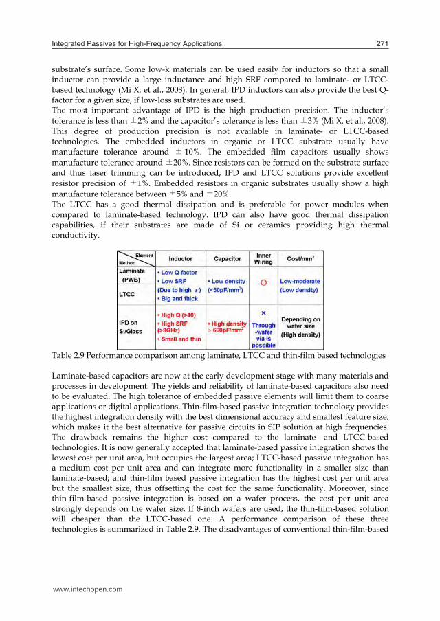
Integrated Passives for High-Frequency Applications 271
Fig. 2.5 Comparison of capacitance values and corresponding capacitor areas between various dielectric materials used for integrated film capacitors Since with thin-film-based passive integration technology the capacitors are formed on the substrate surface, ultra-thin high-k dielectric film with good film quality can also be deposited for capacitors so that a relatively high capacitance density can be achieved. A 0.1 μm SiNx film can offer a capacitance density over 600 pF/mm2. Higher capacitance densities are also possible at the expense of the breakdown voltage reduction by using an ultrathin film (less than 50 nm). Based on HiDTC (high-density-trench capacitor) architecture, a 35 nF/mm2 MIM capacitor has been developed with an Al2O3 dielectric of 20 nm. Embedded inductors in an organic subatrate offering an inductance of up to 30 nH have been reported (Govind V. et al., 2006). LTCC are usefule for integating inductors less than 10nH. For IPD (thin-film-based solution), inductance up to 30nH at a size of less than φ0.6 mm has been reported (Mi X. et al., 2008). Mike Gaynor provided a good case study, in which performances of integrated inductors constructed by laminate, LTCC and Si-IPD respectively are compared in detail (Gaynor M., 2007). For the same inductance, laminate inductors need an area of 5 times that required by IPD. LTCC inductors, which have increasing thickness because more layers are used, have a steep area vs. inductance slope and a slightly increased area compared to IPD inductors. Since the laminate or LTCC-based methods build the passives into the substrate, the quality factor of the built-in inductor will be low and the inductor size will be large due to a relatively large dielectric constant and loss tangent of the substrate materials. The typical inductor diameters are in the order of 1mm. To obtain a large Q-factor and a high self-resonance frequency (SRF) for RF applications, the traces of the coils have to be separated a lot and more layers have to be used. That is to say, low-k materials are preferable for inductor performance. Elsewhere, the typical capacitance density of built-in capacitors is a few pF/mm2 at present, which is still low from the viewpoint of module miniaturization. It is usually difficult to introduce a very thin insulation layer into these two technologies, so high-k insulators are favorable for obtaining a large capacitance. However introducing low-k and high-k insulators into the same substrate will drastically increase the fabrication complexity and cost. IPDs are fabricated using photolithography and thin-film technology, enabling a fine structure and high integration density. The inductors and capacitors are formed on the
substrate’s surface. Some low-k materials can be used easily for inductors so that a small inductor can provide a large inductance and high SRF compared to laminate- or LTCC- based technology (Mi X. et al., 2008). In general, IPD inductors can also provide the best Q-factor for a given size, if low-loss substrates are used. The most important advantage of IPD is the high production precision. The inductor’s tolerance is less than ±2% and the capacitor’s tolerance is less than ±3% (Mi X. et al., 2008). This degree of production precision is not available in laminate- or LTCC-based technologies. The embedded inductors in organic or LTCC substrate usually have manufacture tolerance around ± 10%. The embedded film capacitors usually shows manufacture tolerance around ±20%. Since resistors can be formed on the substrate surface and thus laser trimming can be introduced, IPD and LTCC solutions provide excellent resistor precision of ±1%. Embedded resistors in organic substrates usually show a high manufacture tolerance between ±5% and ±20%. The LTCC has a good thermal dissipation and is preferable for power modules when compared to laminate-based technology. IPD can also have good thermal dissipation capabilities, if their substrates are made of Si or ceramics providing high thermal conductivity.
Table 2.9 Performance comparison among laminate, LTCC and thin-film based technologies Laminate-based capacitors are now at the early development stage with many materials and processes in development. The yields and reliability of laminate-based capacitors also need to be evaluated. The high tolerance of embedded passive elements will limit them to coarse applications or digital applications. Thin-film-based passive integration technology provides the highest integration density with the best dimensional accuracy and smallest feature size, which makes it the best alternative for passive circuits in SIP solution at high frequencies. The drawback remains the higher cost compared to the laminate- and LTCC-based technologies. It is now generally accepted that laminate-based passive integration shows the lowest cost per unit area, but occupies the largest area; LTCC-based passive integration has a medium cost per unit area and can integrate more functionality in a smaller size than laminate-based; and thin-film based passive integration has the highest cost per unit area but the smallest size, thus offsetting the cost for the same functionality. Moreover, since thin-film-based passive integration is based on a wafer process, the cost per unit area strongly depends on the wafer size. If 8-inch wafers are used, the thin-film-based solution will cheaper than the LTCC-based one. A performance comparison of these three technologies is summarized in Table 2.9. The disadvantages of conventional thin-film-based
www.intechopen.com
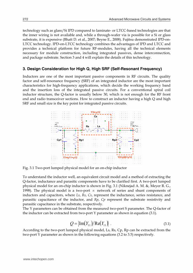
Advanced Microwave Circuits and Systems272
technology such as glass/Si IPD compared to laminate- or LTCC-based technologies are that the inner wiring is not available and, while a through-wafer via is possible for a Si or glass substrate, it is expensive (Bhatt D. et al., 2007; Beyne E., 2008). Fujitsu demonstrated IPD-on-LTCC technology. IPD-on-LTCC technology combines the advantages of IPD and LTCC and provides a technical platform for future RF-modules, having all the technical elements necessary for module construction, including integrated passives, dense interconnection, and package substrate. Section 3 and 4 will explain the details of this technology.
3. Design Consideration for High Q, High SRF (Self-Resonant Frequency)
Inductors are one of the most important passive components in RF circuits. The quality factor and self-resonance frequency (SRF) of an integrated inductor are the most important characteristics for high-frequency applications, which decide the working frequency band and the insertion loss of the integrated passive circuits. For a conventional spiral coil inductor structure, the Q-factor is usually below 30, which is not enough for the RF front end and radio transceiver sections. How to construct an inductor having a high Q and high SRF and small size is the key point for integrated passive circuits.
Cs
Rs Ls
Cp1 Cp2Rp1 Rp2
Y1=y11+y12
Y3=-y12
Y2=y22+y12
Cs
Rs Ls
Cp1 Cp2Rp1 Rp2
Y1=y11+y12
Y3=-y12
Y2=y22+y12
Fig. 3.1 Two-port lumped physical model for an on-chip inductor To understand the inductor well, an equivalent circuit model and a method of extracting the Q-factor, inductance and parasitic components have to be clarified first. A two-port lumped physical model for an on-chip inductor is shown in Fig. 3.1 (Niknejad A. M. &, Meyer R. G., 1998). The physical model is a two-port π network of series and shunt components of inductors and capacitors, where Ls, Rs, Cs, represent the inductance, series resistance, and parasitic capacitance of the inductor, and Rp, Cp represent the substrate resistivity and parasitic capacitance in the substrate, respectively. The Y parameters can be obtained from the measured two-port S parameter. The Q-factor of the inductor can be extracted from two-port Y parameter as shown in equation (3.1).
1111 ReIm YYQ . (3.1)
According to the two-port lumped physical model, Ls, Rs, Cp, Rp can be extracted from the two-port Y parameter as shown in the following equations (3.2 to 3.5) respectively.
12
1Im21
YfLs (3.2)
12
1ReY
Rs (3.3)
1211Im21 YYf
C p (3.4)
1211
1ReYY
Rp . (3.5)
The quality of an inductor is evaluated by its Q factor, which is generally defined as
cyclenoscillatiooneinlossenergy
storedenergyQ
2 . (3.6)
It is inevitable that some parasitic capacitances will occur in a real inductor. For an inductor, only the energy stored in the magnetic field is of interest. Any energy stored in the electric field due to the parasitic capacitances is counterproductive. Thus the Q-factor of an inductor should be given by equation (3.7) (Yue C. P. & Wong S. S., 1998)
2
0
12
2ff
fLR
cyclenoscillatiooneinlossenergyenergyelectricpeakenergymagneticpeakQ
. (3.7)
Fig 3.2 One-port physical model of an inductor including parasitic effects For simplicity, an one-port physical model including parasitic effect as shown in Fig. 3.2, is used to derive the expression of the Q value. According to one-port physical model including parasitic effects, the energies stored in the magnetic and electric fields and lost can be expresses in eqation (3.8 to 3.10) respectively.
www.intechopen.com
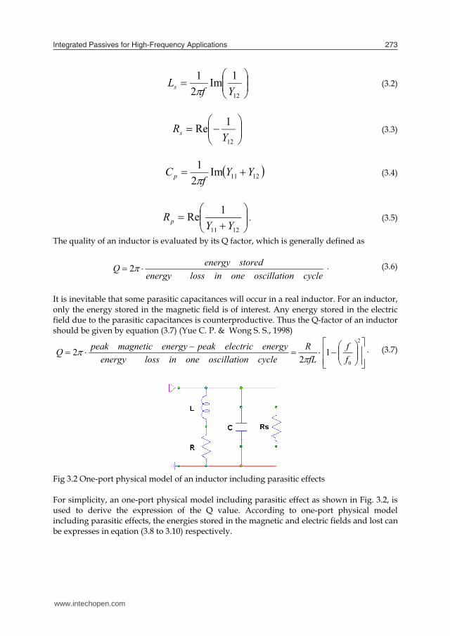
Integrated Passives for High-Frequency Applications 273
technology such as glass/Si IPD compared to laminate- or LTCC-based technologies are that the inner wiring is not available and, while a through-wafer via is possible for a Si or glass substrate, it is expensive (Bhatt D. et al., 2007; Beyne E., 2008). Fujitsu demonstrated IPD-on-LTCC technology. IPD-on-LTCC technology combines the advantages of IPD and LTCC and provides a technical platform for future RF-modules, having all the technical elements necessary for module construction, including integrated passives, dense interconnection, and package substrate. Section 3 and 4 will explain the details of this technology.
3. Design Consideration for High Q, High SRF (Self-Resonant Frequency)
Inductors are one of the most important passive components in RF circuits. The quality factor and self-resonance frequency (SRF) of an integrated inductor are the most important characteristics for high-frequency applications, which decide the working frequency band and the insertion loss of the integrated passive circuits. For a conventional spiral coil inductor structure, the Q-factor is usually below 30, which is not enough for the RF front end and radio transceiver sections. How to construct an inductor having a high Q and high SRF and small size is the key point for integrated passive circuits.
Cs
Rs Ls
Cp1 Cp2Rp1 Rp2
Y1=y11+y12
Y3=-y12
Y2=y22+y12
Cs
Rs Ls
Cp1 Cp2Rp1 Rp2
Y1=y11+y12
Y3=-y12
Y2=y22+y12
Fig. 3.1 Two-port lumped physical model for an on-chip inductor To understand the inductor well, an equivalent circuit model and a method of extracting the Q-factor, inductance and parasitic components have to be clarified first. A two-port lumped physical model for an on-chip inductor is shown in Fig. 3.1 (Niknejad A. M. &, Meyer R. G., 1998). The physical model is a two-port π network of series and shunt components of inductors and capacitors, where Ls, Rs, Cs, represent the inductance, series resistance, and parasitic capacitance of the inductor, and Rp, Cp represent the substrate resistivity and parasitic capacitance in the substrate, respectively. The Y parameters can be obtained from the measured two-port S parameter. The Q-factor of the inductor can be extracted from two-port Y parameter as shown in equation (3.1).
1111 ReIm YYQ . (3.1)
According to the two-port lumped physical model, Ls, Rs, Cp, Rp can be extracted from the two-port Y parameter as shown in the following equations (3.2 to 3.5) respectively.
12
1Im21
YfLs (3.2)
12
1ReY
Rs (3.3)
1211Im21 YYf
C p (3.4)
1211
1ReYY
Rp . (3.5)
The quality of an inductor is evaluated by its Q factor, which is generally defined as
cyclenoscillatiooneinlossenergy
storedenergyQ
2 . (3.6)
It is inevitable that some parasitic capacitances will occur in a real inductor. For an inductor, only the energy stored in the magnetic field is of interest. Any energy stored in the electric field due to the parasitic capacitances is counterproductive. Thus the Q-factor of an inductor should be given by equation (3.7) (Yue C. P. & Wong S. S., 1998)
2
0
12
2ff
fLR
cyclenoscillatiooneinlossenergyenergyelectricpeakenergymagneticpeakQ
. (3.7)
Fig 3.2 One-port physical model of an inductor including parasitic effects For simplicity, an one-port physical model including parasitic effect as shown in Fig. 3.2, is used to derive the expression of the Q value. According to one-port physical model including parasitic effects, the energies stored in the magnetic and electric fields and lost can be expresses in eqation (3.8 to 3.10) respectively.
www.intechopen.com
Advanced Microwave Circuits and Systems274
22
20
2 RLLVE magneticpeak
(3.8)
2
20 CVE electricpeak
(3.9)
22
20 12
2RL
RR
VEs
cyclenoscillatiooneinloss
. (3.10)
Where R represents the series resistance of the inductor; C represents the total parasitic capacitance including that of the inductor and substrate; Rs represents the substrate resistivity and V0 denotes the peak voltage at the inductor port. The inductor Q-factor can be obtained as shown in equation 3.11 by substituting equations 3.8 to 3.10 into 3.7.
LCLCR
RRLRR
RLQ
s
s 22
2 11/
. (3.11)
The Q-factor in the equation 3.11 is expressed as a product of three factors, where the first factor is called the ideal Q factor, the second factor is called the substrate loss factor, and the third factor is called the self-resonance factor. The inductance L is defined as L=φ/I, here φ is the magnetic flux crossing the inductor coil and I is the current flowing through the coil. The multi-layered coil inductor produces a large inductance, L, as an entire inductor because the multi-layered coil shows mutual inductance due to mutual electromagnetic induction between the multiple coils connected in series and thus increase the magnetic flux crossing the inductor coil. For this reason, according to the multi-layered coil inductor, the total length of conductive wire necessary for achieving a given inductance L tends to be short. The shorter the total length of the conductive wire for constituting the multi-layered coil inductor, the smaller the resistance R in the multi-layered coil inductor tends to be. As can be seen in the above-mentioned first factor, achieving a predetermined inductance L at a small resistance R contributes to an increase in the Q-factor. The inductor coils have to be constructed with good conductivity. The width and height of the coil traces have to be designed carefully to ensure low RF resistance at operating frequencies. The second factor in equation 3.11 suggests that a substrate having high resistivity Rs should be used to lower the loss from the substrate and to increase the second factor so that it is 1. For this reason, ceramic, glass, or fused quartz are suitable for the substrate. The third factor of equation 3.11 suggests that the parasitic capacitance C should be lowered. As can be seen from the above-mentioned third factor, making the parasitic capacitance C zero brings this factor close to 1 and contributes to an increase in the Q-factor. Further, lowering of the parasitic capacitance is also favourable for achieving a good high-frequency performance. The self-resonant frequency (SRF) f0 of an inductor can be determined when the third factor of equation 3.11 becomes zero. Using this self-resonance condition, the same result as equation 1.6 is then obtained.
2
2121
LR
LCfo . (3.12)
Generally, the smaller the parasitic capacitance of the inductor, the greater is the inductor’s SRF shift toward the high frequency side, making it easier to achieve a good high-frequency characteristic. For these reasons, we recommend using the two-layered coil in the air, as no material has a dielectric constant that is lower than air. As discussed above, the optimized structure of the IPD is illustrated in Fig. 3.3 (Mi X. et al., 2007). The lower spiral coil is directly formed on the substrate and the upper coil is freestanding in the air. Air is used as the insulation layer between the two coils to minimize the parasitic capacitance in the coil inductor. The two spiral coils are connected in series by a metal via and the direction of the electric current flowing through the two coils is the same. The direction of the magnetic flux occurring in the two coils agrees, and the total magnetic flux crossing the two-layered coil increases. The two coils are arranged to overlap with each other to further maximize the mutual induction. There are no support poles under the upper coil, nor are there intersections between the wiring and the coils in the two-layered coil structure. It also helps to prevent an extra eddy current loss from occurring in these sections and maximizing the Q-factor of the coil inductor. The capacitor is of a metal-insulator-metal structure, as shown in Fig. 3.3 (c). A thick metal is used for the lower and upper electrodes of the capacitor to suppress the loss and parasitic inductance arising in the electrodes and thus to enlarge the Q-factor of the capacitor and its self-resonant-frequency. A 3D interconnection in the air is introduced for the upper electrode to help eliminate the parasitic capacitance that results from the wiring to the MIM capacitor.
(a) Fujitsu’s IPD
Coil part
2-layered coil in the air
Capacitor part
Interconnect in the air
(b) Coil part (c) Capacitor part Fig. 3.3 High-Q IPD configuration
www.intechopen.com

Integrated Passives for High-Frequency Applications 275
22
20
2 RLLVE magneticpeak
(3.8)
2
20 CVE electricpeak
(3.9)
22
20 12
2RL
RR
VEs
cyclenoscillatiooneinloss
. (3.10)
Where R represents the series resistance of the inductor; C represents the total parasitic capacitance including that of the inductor and substrate; Rs represents the substrate resistivity and V0 denotes the peak voltage at the inductor port. The inductor Q-factor can be obtained as shown in equation 3.11 by substituting equations 3.8 to 3.10 into 3.7.
LCLCR
RRLRR
RLQ
s
s 22
2 11/
. (3.11)
The Q-factor in the equation 3.11 is expressed as a product of three factors, where the first factor is called the ideal Q factor, the second factor is called the substrate loss factor, and the third factor is called the self-resonance factor. The inductance L is defined as L=φ/I, here φ is the magnetic flux crossing the inductor coil and I is the current flowing through the coil. The multi-layered coil inductor produces a large inductance, L, as an entire inductor because the multi-layered coil shows mutual inductance due to mutual electromagnetic induction between the multiple coils connected in series and thus increase the magnetic flux crossing the inductor coil. For this reason, according to the multi-layered coil inductor, the total length of conductive wire necessary for achieving a given inductance L tends to be short. The shorter the total length of the conductive wire for constituting the multi-layered coil inductor, the smaller the resistance R in the multi-layered coil inductor tends to be. As can be seen in the above-mentioned first factor, achieving a predetermined inductance L at a small resistance R contributes to an increase in the Q-factor. The inductor coils have to be constructed with good conductivity. The width and height of the coil traces have to be designed carefully to ensure low RF resistance at operating frequencies. The second factor in equation 3.11 suggests that a substrate having high resistivity Rs should be used to lower the loss from the substrate and to increase the second factor so that it is 1. For this reason, ceramic, glass, or fused quartz are suitable for the substrate. The third factor of equation 3.11 suggests that the parasitic capacitance C should be lowered. As can be seen from the above-mentioned third factor, making the parasitic capacitance C zero brings this factor close to 1 and contributes to an increase in the Q-factor. Further, lowering of the parasitic capacitance is also favourable for achieving a good high-frequency performance. The self-resonant frequency (SRF) f0 of an inductor can be determined when the third factor of equation 3.11 becomes zero. Using this self-resonance condition, the same result as equation 1.6 is then obtained.
2
2121
LR
LCfo . (3.12)
Generally, the smaller the parasitic capacitance of the inductor, the greater is the inductor’s SRF shift toward the high frequency side, making it easier to achieve a good high-frequency characteristic. For these reasons, we recommend using the two-layered coil in the air, as no material has a dielectric constant that is lower than air. As discussed above, the optimized structure of the IPD is illustrated in Fig. 3.3 (Mi X. et al., 2007). The lower spiral coil is directly formed on the substrate and the upper coil is freestanding in the air. Air is used as the insulation layer between the two coils to minimize the parasitic capacitance in the coil inductor. The two spiral coils are connected in series by a metal via and the direction of the electric current flowing through the two coils is the same. The direction of the magnetic flux occurring in the two coils agrees, and the total magnetic flux crossing the two-layered coil increases. The two coils are arranged to overlap with each other to further maximize the mutual induction. There are no support poles under the upper coil, nor are there intersections between the wiring and the coils in the two-layered coil structure. It also helps to prevent an extra eddy current loss from occurring in these sections and maximizing the Q-factor of the coil inductor. The capacitor is of a metal-insulator-metal structure, as shown in Fig. 3.3 (c). A thick metal is used for the lower and upper electrodes of the capacitor to suppress the loss and parasitic inductance arising in the electrodes and thus to enlarge the Q-factor of the capacitor and its self-resonant-frequency. A 3D interconnection in the air is introduced for the upper electrode to help eliminate the parasitic capacitance that results from the wiring to the MIM capacitor.
(a) Fujitsu’s IPD
Coil part
2-layered coil in the air
Capacitor part
Interconnect in the air
(b) Coil part (c) Capacitor part Fig. 3.3 High-Q IPD configuration
www.intechopen.com

Advanced Microwave Circuits and Systems276
4. IPD on LTCC technology
4.1 Concept We propose a new technology to combine the advantages of LTCC and IPD technology. High-Q passive circuits using a two-layered aerial spiral coil structure and 3D interconnection in the air are constructed directly on an LTCC wiring wafer. This technology is a promising means of miniaturizing the next generation of RF-modules A conceptual schematic diagram of the proposed IPD on the LTCC for the RF module applications is illustrated in Fig. 4.1. The above-mentioned high-Q IPD is directly formed on the LTCC wiring wafer. Functional devices such as the ICs are mounted above the IPD, while the LTCC wiring wafer has metal vias on the surface for electrical interconnection between the wiring wafer and the integrated passive circuit or the mounted function device chips. Pads are formed on the reverse side of the LTCC wafer to provide input and output paths to the motherboard. The inner wiring of the LTCC wafer can provide very dense interconnects between the passive circuit and the functional devices. Because the function device chips are installed above the integrated passives, the chip-mounting efficiency can approach 100%, which means a chip-sized module can be realized.
Fig.4.1. Conceptual schematic diagram of the proposed IPD on LTCC for RF module applications
4.2 Development The fabrication technology of the high-Q IPD on LTCC is shown in Fig. 4.2. The basic concept is to form a large-size LTCC wiring wafer, and then to form the IPD directly on the wafer surface. First, an LTCC wiring wafer is fabricated, and the surface of the wafer is subject to a smoothing process. The surface roughness needs to be reduced to ensure that the wafers can go through the following photolithography and thin-film formation processes. The capacitors, lower coils and interconnects are then formed by thin-film technology and electrical plating technology. Next, a sacrificial layer is formed, which has the same height as that of the lower metal structure. At the via positions, windows are opened in the sacrificial layer to facilitate an electrical connection between the upper and lower metal structure. On the sacrifice layer, a metal seed layer is formed for the following electrical plating process. After that, the upper coils and interconnects as well as the bumps for interconnection between the function device chips and IPD wafer are formed by electrical plating technology. The metal seed layer and the sacrificial layer are then removed to release the integrated passives. The upper and lower metal structures are made of copper and the bumps are gold-plated. Function device chips such as the IC can be mounted onto the bumps by flip-chip
bonding technology. If necessary, a sealing or under-filling process can be conducted. Finally, the module units are created by cutting the wafer. All of the fabrication processes are carried out at wafer level, which leads to high productivity. The fabricated high-Q IPD on LTCC wiring substrate is shown in Fig. 4.3.
Fig. 4.2. Fabrication technology of the high-Q IPD on LTCC
Fig. 4.3. Fabricated high-Q IPD on LTCC wiring substrate We inspected the performance of the fabricated high-Q IPD on LTCC wiring wafer. Figure 4.4. shows a performance comparison between a two-layer coil in the air and a one-layer coil in resin. The two coils have the same inductance of 12 nH, but differ in coil size. The two-layer coil is 350um in diameter, and the one-layer coil in resin is 400um in diameter. The two-layer coil can represent a 30% saving in area while providing the same inductance. The developed two-layered coils can achieve an inductance of up to 30nH at a size of less than φ0.6 mm. For a given size, the two-layer coil in the air improves the Q-factor by 1.7 to 2 times that of the conventional one-layer coil in the resin. Moreover, the SRF also increases from 7.5 GHz to 8.5 GHz. It indicates that the two-layered coil in the air is more suitable for
www.intechopen.com
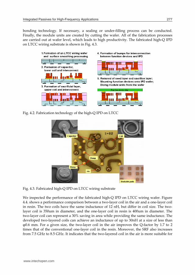
Integrated Passives for High-Frequency Applications 277
4. IPD on LTCC technology
4.1 Concept We propose a new technology to combine the advantages of LTCC and IPD technology. High-Q passive circuits using a two-layered aerial spiral coil structure and 3D interconnection in the air are constructed directly on an LTCC wiring wafer. This technology is a promising means of miniaturizing the next generation of RF-modules A conceptual schematic diagram of the proposed IPD on the LTCC for the RF module applications is illustrated in Fig. 4.1. The above-mentioned high-Q IPD is directly formed on the LTCC wiring wafer. Functional devices such as the ICs are mounted above the IPD, while the LTCC wiring wafer has metal vias on the surface for electrical interconnection between the wiring wafer and the integrated passive circuit or the mounted function device chips. Pads are formed on the reverse side of the LTCC wafer to provide input and output paths to the motherboard. The inner wiring of the LTCC wafer can provide very dense interconnects between the passive circuit and the functional devices. Because the function device chips are installed above the integrated passives, the chip-mounting efficiency can approach 100%, which means a chip-sized module can be realized.
Fig.4.1. Conceptual schematic diagram of the proposed IPD on LTCC for RF module applications
4.2 Development The fabrication technology of the high-Q IPD on LTCC is shown in Fig. 4.2. The basic concept is to form a large-size LTCC wiring wafer, and then to form the IPD directly on the wafer surface. First, an LTCC wiring wafer is fabricated, and the surface of the wafer is subject to a smoothing process. The surface roughness needs to be reduced to ensure that the wafers can go through the following photolithography and thin-film formation processes. The capacitors, lower coils and interconnects are then formed by thin-film technology and electrical plating technology. Next, a sacrificial layer is formed, which has the same height as that of the lower metal structure. At the via positions, windows are opened in the sacrificial layer to facilitate an electrical connection between the upper and lower metal structure. On the sacrifice layer, a metal seed layer is formed for the following electrical plating process. After that, the upper coils and interconnects as well as the bumps for interconnection between the function device chips and IPD wafer are formed by electrical plating technology. The metal seed layer and the sacrificial layer are then removed to release the integrated passives. The upper and lower metal structures are made of copper and the bumps are gold-plated. Function device chips such as the IC can be mounted onto the bumps by flip-chip
bonding technology. If necessary, a sealing or under-filling process can be conducted. Finally, the module units are created by cutting the wafer. All of the fabrication processes are carried out at wafer level, which leads to high productivity. The fabricated high-Q IPD on LTCC wiring substrate is shown in Fig. 4.3.
Fig. 4.2. Fabrication technology of the high-Q IPD on LTCC
Fig. 4.3. Fabricated high-Q IPD on LTCC wiring substrate We inspected the performance of the fabricated high-Q IPD on LTCC wiring wafer. Figure 4.4. shows a performance comparison between a two-layer coil in the air and a one-layer coil in resin. The two coils have the same inductance of 12 nH, but differ in coil size. The two-layer coil is 350um in diameter, and the one-layer coil in resin is 400um in diameter. The two-layer coil can represent a 30% saving in area while providing the same inductance. The developed two-layered coils can achieve an inductance of up to 30nH at a size of less than φ0.6 mm. For a given size, the two-layer coil in the air improves the Q-factor by 1.7 to 2 times that of the conventional one-layer coil in the resin. Moreover, the SRF also increases from 7.5 GHz to 8.5 GHz. It indicates that the two-layered coil in the air is more suitable for
www.intechopen.com

Advanced Microwave Circuits and Systems278
high-frequency applications exceeding 3GHz where hardly any surface-mounting devices (SMD) usually work well due to the low SRF.
0
10
20
30
40
50
60
70
80
0 2 4 6 8 10
周波数 [G Hz]
L [nH] 又は
Q
中空二層
従来構造
L
Q
2-stage in airΦ350μm; 5.5T1-stage coil in resinΦ400μm; 5.5T
Q-fa
ctor
[A.U
.] &
L [n
H]
Frequency [GHz]
0
10
20
30
40
50
60
70
80
0 2 4 6 8 10
周波数 [G Hz]
L [nH] 又は
Q
中空二層
従来構造
L
Q
2-stage in airΦ350μm; 5.5T1-stage coil in resinΦ400μm; 5.5T
Q-fa
ctor
[A.U
.] &
L [n
H]
Frequency [GHz]
Fig. 4.4. Performance comparison between a two-layer coil in the air and a one-layer coil embedded in resin
Fig. 4.5. Q-factor comparison between Fujitsu’s 2-layered IPD and those made by other companies and SMD inductors on a similar size basis Q-factor comparison between Fujitsu’s 2-layered aerial spiral coil and those made by other companies and SMD inductors are compared at 2 GHz in Fig. 4.5. In general, the Q-factor of an inductor strongly depends on inductor size. Fujitsu IPD inductors have an outer diameter smaller than 0.6 mm. Those points for the integrated inductors reported by other research organizations have a similar size to Fujitsu’s IPD inductor. The SMD inductors compared in Fig. 4.5. have the a size of 0.6 mm×0.3 mm. The conventional 1-layer integrated spiral coils in resin with a size less than 0.6 mm square can only offer a Q-factor of less than 30. These off-chip inductors (SMD) with the similar a size of 0.6 mm×0.3 mm can offer a Q-factor
higher than 40 only when the inductance is less than 5 nH. When the inductance increases, the Q-factor rapidly declines to less than 30. As a result, Fujitsu’s 2-layered aerial spiral coil can provide a performance that is superior to its rivals of a similar size.
50
100
150
200
250
0.5 1 1.5 2 2.5 3 3.5 4
Frequency [GHz]
Q-fa
ctor
[A.U
.]
Fig. 4.6. Performance comparison between a capacitor using a 3D interconnect in the air and a capacitor embedded in resin
Fig. 4.7. Capacitor performances of Fujitsu’s IPD (a) Dependence of capacitance on frequency (b) Relationship between capacitance and capacitor area The Q-factor comparison between the newly developed capacitor using 3D interconnection in the air and the conventional capacitor embedded in resin is shown in Fig. 4.6. The Q-factor is improved from 110 to 180 at 2 GHz. The other performances of Fujitsu’s IPD capacitors are shown in Fig. 4.7. and Fig. 4.8. Figure 4.7. (a) shows the dependence of the capacitance on frequency and Fig. 4.7. (b) shows the relationship between the capacitance and the capacitor area. As shown in Fig.4.7. (a), the capacitance stays flat up to several GHz, indicating that the developed capacitor has small parasitic inductance and high self-
www.intechopen.com
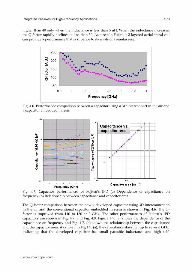
Integrated Passives for High-Frequency Applications 279
high-frequency applications exceeding 3GHz where hardly any surface-mounting devices (SMD) usually work well due to the low SRF.
0
10
20
30
40
50
60
70
80
0 2 4 6 8 10
周波数 [G Hz]
L [nH] 又は
Q
中空二層
従来構造
L
Q
2-stage in airΦ350μm; 5.5T1-stage coil in resinΦ400μm; 5.5T
Q-fa
ctor
[A.U
.] &
L [n
H]
Frequency [GHz]
0
10
20
30
40
50
60
70
80
0 2 4 6 8 10
周波数 [G Hz]
L [nH] 又は
Q
中空二層
従来構造
L
Q
2-stage in airΦ350μm; 5.5T1-stage coil in resinΦ400μm; 5.5T
Q-fa
ctor
[A.U
.] &
L [n
H]
Frequency [GHz]
Fig. 4.4. Performance comparison between a two-layer coil in the air and a one-layer coil embedded in resin
Fig. 4.5. Q-factor comparison between Fujitsu’s 2-layered IPD and those made by other companies and SMD inductors on a similar size basis Q-factor comparison between Fujitsu’s 2-layered aerial spiral coil and those made by other companies and SMD inductors are compared at 2 GHz in Fig. 4.5. In general, the Q-factor of an inductor strongly depends on inductor size. Fujitsu IPD inductors have an outer diameter smaller than 0.6 mm. Those points for the integrated inductors reported by other research organizations have a similar size to Fujitsu’s IPD inductor. The SMD inductors compared in Fig. 4.5. have the a size of 0.6 mm×0.3 mm. The conventional 1-layer integrated spiral coils in resin with a size less than 0.6 mm square can only offer a Q-factor of less than 30. These off-chip inductors (SMD) with the similar a size of 0.6 mm×0.3 mm can offer a Q-factor
higher than 40 only when the inductance is less than 5 nH. When the inductance increases, the Q-factor rapidly declines to less than 30. As a result, Fujitsu’s 2-layered aerial spiral coil can provide a performance that is superior to its rivals of a similar size.
50
100
150
200
250
0.5 1 1.5 2 2.5 3 3.5 4
Frequency [GHz]
Q-fa
ctor
[A.U
.]
Fig. 4.6. Performance comparison between a capacitor using a 3D interconnect in the air and a capacitor embedded in resin
Fig. 4.7. Capacitor performances of Fujitsu’s IPD (a) Dependence of capacitance on frequency (b) Relationship between capacitance and capacitor area The Q-factor comparison between the newly developed capacitor using 3D interconnection in the air and the conventional capacitor embedded in resin is shown in Fig. 4.6. The Q-factor is improved from 110 to 180 at 2 GHz. The other performances of Fujitsu’s IPD capacitors are shown in Fig. 4.7. and Fig. 4.8. Figure 4.7. (a) shows the dependence of the capacitance on frequency and Fig. 4.7. (b) shows the relationship between the capacitance and the capacitor area. As shown in Fig.4.7. (a), the capacitance stays flat up to several GHz, indicating that the developed capacitor has small parasitic inductance and high self-
www.intechopen.com

Advanced Microwave Circuits and Systems280
resonance frequency. The capacitance density of the developed integrated capacitors reaches 200 pF/mm2, which makes it possible to reduce the size while covering almost all RF applications. Ultra-thin insulation film is favorable for achieving a large capacitance density, but has a risk in terms of breakdown voltage. The breakdown voltage characteristic depends strongly on the substrate roughness and quality of the dielectric film used for the capacitor. High-quality thin-film formation technology is the key to realizing high capacitance density. We also checked the breakdown voltage of the integrated capacitors and the result is shown in Fig. 4.7. The average breakdown voltage exceeds 200 V, which is enough for RF module applications.
Fig. 4.8. Break-down voltage of Fujitsu’s IPD capacitors
Fig. 4.9. Production tolerance for two-layered coil in the air
0
5
10
15
20
25
30
1.92
1.94
1.96
1.98
2.00
2.02
2.04
2.06
2.08
2.10
Capacitance (pF)
Prob
abili
ty (%
)
Fig. 4.10. Production tolerance for capacitor using 3D interconnect in the air We inspected the production tolerance of the developed integrated passives. The inductance and Q-factor of 7.1 nH coils fabricated in different production batches were measured. The results are shown in Fig. 4.9. The deviation in inductance is less than ±2%. The deviation in the Q-factor is about ±5%. The capacitance deviation of 2 pF capacitors fabricated in different production batches was evaluated and the result is shown in Fig. 4.10. The deviation in capacitance is less than ±3%. The above-mentioned production tolerance includes the wafer deviation and batch deviation, which is not available in the case for its rivals, namely laminate-based and LTCC-based technologies. High-Q IPD on LTCC technology has been demonstrated for RF-module applications using the newly developed multistage plating technology based on a sacrifice layer. A two-layered aerial spiral coil structure and 3D interconnection in the air are used to increase the quality factor and to reduce the parasitic capacitance. This configuration enables us to achieve a Q-factor of 40 to 6o at 2 GHz for the integrated spiral inductors of a size smaller than φ0.6 mm, while providing a high self-resonance frequency of over 8 GHz. The Q-factor of the capacitors has been improved from 110 to 180 at 2 GHz. Very high production precision has been achieved: less than ±2% for inductors and less than ±3% for capacitors. This technology combines the advantages of LTCC and IPD. The function device chips can be mounted above the IPD. The inner wiring built in the LTCC wafer provides dense interconnection. And the pads on the reverse side allow easy access to the motherboard. This technology combines the advantages of IPD and LTCC and provides a technical platform for future RF-modules, which has all the technical elements necessary for module construction, including integrated passives, dense interconnection, package substrate. These advantages are promising for the miniaturization of RF-modules and the realization of a chip-sized-module.
5. Summary and Discussions
In this chapter, we have concisely reviewed the recent developments in passive integration technologies and design considerations for system miniaturization and high-frequency applications. Over the past 10 years, passive integration technologies, laminate-, LTCC- and thin-film based technologies have gone through a significant evolution to meet the requirements of lower cost solutions, system miniaturization, and high levels of functionality integration, improved reliability, and high-volume applications. Some of them
www.intechopen.com

Integrated Passives for High-Frequency Applications 281
resonance frequency. The capacitance density of the developed integrated capacitors reaches 200 pF/mm2, which makes it possible to reduce the size while covering almost all RF applications. Ultra-thin insulation film is favorable for achieving a large capacitance density, but has a risk in terms of breakdown voltage. The breakdown voltage characteristic depends strongly on the substrate roughness and quality of the dielectric film used for the capacitor. High-quality thin-film formation technology is the key to realizing high capacitance density. We also checked the breakdown voltage of the integrated capacitors and the result is shown in Fig. 4.7. The average breakdown voltage exceeds 200 V, which is enough for RF module applications.
Fig. 4.8. Break-down voltage of Fujitsu’s IPD capacitors
Fig. 4.9. Production tolerance for two-layered coil in the air
0
5
10
15
20
25
30
1.92
1.94
1.96
1.98
2.00
2.02
2.04
2.06
2.08
2.10
Capacitance (pF)
Prob
abili
ty (%
)
Fig. 4.10. Production tolerance for capacitor using 3D interconnect in the air We inspected the production tolerance of the developed integrated passives. The inductance and Q-factor of 7.1 nH coils fabricated in different production batches were measured. The results are shown in Fig. 4.9. The deviation in inductance is less than ±2%. The deviation in the Q-factor is about ±5%. The capacitance deviation of 2 pF capacitors fabricated in different production batches was evaluated and the result is shown in Fig. 4.10. The deviation in capacitance is less than ±3%. The above-mentioned production tolerance includes the wafer deviation and batch deviation, which is not available in the case for its rivals, namely laminate-based and LTCC-based technologies. High-Q IPD on LTCC technology has been demonstrated for RF-module applications using the newly developed multistage plating technology based on a sacrifice layer. A two-layered aerial spiral coil structure and 3D interconnection in the air are used to increase the quality factor and to reduce the parasitic capacitance. This configuration enables us to achieve a Q-factor of 40 to 6o at 2 GHz for the integrated spiral inductors of a size smaller than φ0.6 mm, while providing a high self-resonance frequency of over 8 GHz. The Q-factor of the capacitors has been improved from 110 to 180 at 2 GHz. Very high production precision has been achieved: less than ±2% for inductors and less than ±3% for capacitors. This technology combines the advantages of LTCC and IPD. The function device chips can be mounted above the IPD. The inner wiring built in the LTCC wafer provides dense interconnection. And the pads on the reverse side allow easy access to the motherboard. This technology combines the advantages of IPD and LTCC and provides a technical platform for future RF-modules, which has all the technical elements necessary for module construction, including integrated passives, dense interconnection, package substrate. These advantages are promising for the miniaturization of RF-modules and the realization of a chip-sized-module.
5. Summary and Discussions
In this chapter, we have concisely reviewed the recent developments in passive integration technologies and design considerations for system miniaturization and high-frequency applications. Over the past 10 years, passive integration technologies, laminate-, LTCC- and thin-film based technologies have gone through a significant evolution to meet the requirements of lower cost solutions, system miniaturization, and high levels of functionality integration, improved reliability, and high-volume applications. Some of them
www.intechopen.com

Advanced Microwave Circuits and Systems282
have enabled miniaturized or modularized wireless telecommunication products to be manufactured. Developments in new materials and technologies for laminate-based technology have been significantly advanced. This makes possible the lowest cost integration of embedded resistors, capacitors, and inductors. Embedded discrete passives technology has been used for mass production. The materials and processes of laminate-based film capacitors are now immature and the yields and reliability also need to be evaluated. The large production tolerance due to instabilities in the materials and the fabrication processes remains the drawback. LTCC-based passive integration has high material reliability, good thermal dissipation and relatively high integration density compared to laminate-based technologies, but has the common drawback of a large production tolerance due to the screen-printed conductors and the shrinkage during the firing process. The high tolerance of embedded passive elements in organic or LTCC substrate limits their use to coarse applications or digital applications. The thin film based passive integration, usually is called as integrated passive device (IPD) provides the highest integration density with the best dimensional accuracy and smallest feature size, which makes it the most powerful technology for passives integration in SIP solution at high frequencies. When a large wafer size is used for IPD, the cost per unit area will be drastically reduced and can compete with laminate- and LTCC-based technologies at the same functionality. A small size, high Q-factor, high SRF, and large inductance are required for integrated inductors to meet the demands for high-frequency performances and low cost. Conventional spiral coils cannot meet these requirements at the same time. We have established process technology to produce IPD using 2-layered coil in the air and confirmed its good performance. ・ 2-layered coil in air : Q≧40@2 GHz; Q≧[email protected] GHz with a coil size less than 0.6 mm ・ Capacitor: 200 pF/mm2 density and break-down voltage over 200 v. For integrated capacitors, the capacitance density should be increased by introducing a high-k thin film with good film quality. This will help increase the capabilities of integrating large capacitance or scaling-down the capacitor size. Current IPD technologies such as IPD on glass/Si, have disadvantages compared to laminate- or LTCC-based technologies, namely the inner wiring is not available and, while a through-wafer via is possible for a Si or glass substrate, it is expensive. This will result in limitations for future system level integration including size, complexity and cost. We demonstrated IPD-on-LTCC technology, which combines the advantages of IPD and LTCC and provides a technical platform for future RF-modules, and which has all the technical elements necessary for module construction, including integrated passives, dense interconnection, and package substrate. These advantages are promising for the miniaturization of RF-modules and the realization of a chip-sized-module to meet the future market demand for higher levels of integration and miniaturization. In the future, system integration will become more complicated and involve more and more functions of the package, such as sensors, actuators, MEMS, or power supply components. For example, decoupling, filtering and switching are all electrical functions which cannot be effectively integrated on active silicon nowadays, but which are required for the generic circuit blocks of high-frequency radio front ends. Moreover, tunable capabilities are strongly expected to offer more flexible radio front-ends for future software-defined-radio or cognitive radio systems. MEMS devices have shown promise for realizing tuning functions.
Incorporating RF-MEMS components such as switches, variable capacitors and tunable filters, in RF-module platforms will drastically increase the functionality and will be the next challenging development. When constructing such complicated 3D built-up systems, system electro-magnetic field modeling will become more difficult and challenging. In addition, thermal and current as well as mechanical stress management will have to be taken into account from the beginning of the system concept. Setting up a well-established design methodology with capabilities to design and optimize extensive components including active, passive and MEMS devices is also important and is a future task.
6. References
Allers K. -H.; Brenner P. & Schrenk M. (2003). Dielectric Reliability and Material Properties of Al203 in Metal Insulator Metal capacitors (MIMCAP) for RF Bipolar technologies in comparison to SiO2, SiN and Ta205, Proceedings of BCTM, Toulouse, France, 2003, pp. 35-38
Arnold R. G.; Faulkner C. C. & Pedder D. J. (1997). Silicon MCM-D Technology for RF Integration, Proceedings of Ineternational Conference on Multichip Modules IEEE, pp. 340-344, 2-4 April 1997
Bahl I. & Bhartia P. (2003). Microwave Solid State Circuit Design, John Wiley & Sons, ISBN 0-471-20755-1, Hoboken, New Jersey
Banieki J. D. et al. (1998). Dielectric relaxation of Ba0.7Sr0.3TiO3 thin film from 1 mHz to 20 GHz, Appl. Phys. Lett., 72(4), 26 January 1998, pp. 498-500
Bauer W.; Purger S. & Schrittwieser W. (2003). Embedded Passive Technology form a PCB Maker's Perspective, Circuitree, October 1, 2003
Beique G. et al. (2006). Dry Etching of High-K Dielectric PZT Stacks for Integrated Passive Devices, Integrated Ferroelectrics, Vol. 86, 2006, pp. 49–56, Taylor & Francis Group, LLC, ISSN 1058-4587
Berthelot A. et al. (2007), Highly Reliable TiN/ZrO2/TiN 3D Stacked Capacitors for 45 nm Embedded DRAM Technologies, Proceedings of IEEE ESSDERC, Montreux, Switzerland, 2006, pp. 343-346
Beyne E. (2008). Solving Technical and Economical Barriers to the Adoption of Through-Si-Via 3D Integration Technologies, Proceedings of 10th Electronics Packaging Technology Conference, 2008, pp. 29-34
Bhatt D. et al. (2007). Process Optimisation and Characterization of Excimer Laser Drilling of Microvias in Glass, Proceedings of 9th Electronics Packaging Technology Conference, 2007, pp. 196-201
Borland W. et al. (2002). Embedded Singulated Ceramic Passives in Printed Wring Boards, Proceeding of the IMAPS-Advanced Technology Workshop on Passive Integration, Ogunquit, Maine, June 2002
Brown R. L.; Polinski P. W. & Shaikh A. S. (1994). MANUFACTURING OF MICROWAVE MODULES USING LOW-TEMPERATURE COFIRED CERAMICS, Proceedings of IEEE MTT-S International Microwave Symposium (IMS), pp. 1727-1730, 1994.
Carchon G. et al. (2001). Multi-layer thin-film MCM-D for the integration of high performance wireless front-end systems, Microw. J., Vol. 44, 2001, pp. 96–110
www.intechopen.com

Integrated Passives for High-Frequency Applications 283
have enabled miniaturized or modularized wireless telecommunication products to be manufactured. Developments in new materials and technologies for laminate-based technology have been significantly advanced. This makes possible the lowest cost integration of embedded resistors, capacitors, and inductors. Embedded discrete passives technology has been used for mass production. The materials and processes of laminate-based film capacitors are now immature and the yields and reliability also need to be evaluated. The large production tolerance due to instabilities in the materials and the fabrication processes remains the drawback. LTCC-based passive integration has high material reliability, good thermal dissipation and relatively high integration density compared to laminate-based technologies, but has the common drawback of a large production tolerance due to the screen-printed conductors and the shrinkage during the firing process. The high tolerance of embedded passive elements in organic or LTCC substrate limits their use to coarse applications or digital applications. The thin film based passive integration, usually is called as integrated passive device (IPD) provides the highest integration density with the best dimensional accuracy and smallest feature size, which makes it the most powerful technology for passives integration in SIP solution at high frequencies. When a large wafer size is used for IPD, the cost per unit area will be drastically reduced and can compete with laminate- and LTCC-based technologies at the same functionality. A small size, high Q-factor, high SRF, and large inductance are required for integrated inductors to meet the demands for high-frequency performances and low cost. Conventional spiral coils cannot meet these requirements at the same time. We have established process technology to produce IPD using 2-layered coil in the air and confirmed its good performance. ・ 2-layered coil in air : Q≧40@2 GHz; Q≧[email protected] GHz with a coil size less than 0.6 mm ・ Capacitor: 200 pF/mm2 density and break-down voltage over 200 v. For integrated capacitors, the capacitance density should be increased by introducing a high-k thin film with good film quality. This will help increase the capabilities of integrating large capacitance or scaling-down the capacitor size. Current IPD technologies such as IPD on glass/Si, have disadvantages compared to laminate- or LTCC-based technologies, namely the inner wiring is not available and, while a through-wafer via is possible for a Si or glass substrate, it is expensive. This will result in limitations for future system level integration including size, complexity and cost. We demonstrated IPD-on-LTCC technology, which combines the advantages of IPD and LTCC and provides a technical platform for future RF-modules, and which has all the technical elements necessary for module construction, including integrated passives, dense interconnection, and package substrate. These advantages are promising for the miniaturization of RF-modules and the realization of a chip-sized-module to meet the future market demand for higher levels of integration and miniaturization. In the future, system integration will become more complicated and involve more and more functions of the package, such as sensors, actuators, MEMS, or power supply components. For example, decoupling, filtering and switching are all electrical functions which cannot be effectively integrated on active silicon nowadays, but which are required for the generic circuit blocks of high-frequency radio front ends. Moreover, tunable capabilities are strongly expected to offer more flexible radio front-ends for future software-defined-radio or cognitive radio systems. MEMS devices have shown promise for realizing tuning functions.
Incorporating RF-MEMS components such as switches, variable capacitors and tunable filters, in RF-module platforms will drastically increase the functionality and will be the next challenging development. When constructing such complicated 3D built-up systems, system electro-magnetic field modeling will become more difficult and challenging. In addition, thermal and current as well as mechanical stress management will have to be taken into account from the beginning of the system concept. Setting up a well-established design methodology with capabilities to design and optimize extensive components including active, passive and MEMS devices is also important and is a future task.
6. References
Allers K. -H.; Brenner P. & Schrenk M. (2003). Dielectric Reliability and Material Properties of Al203 in Metal Insulator Metal capacitors (MIMCAP) for RF Bipolar technologies in comparison to SiO2, SiN and Ta205, Proceedings of BCTM, Toulouse, France, 2003, pp. 35-38
Arnold R. G.; Faulkner C. C. & Pedder D. J. (1997). Silicon MCM-D Technology for RF Integration, Proceedings of Ineternational Conference on Multichip Modules IEEE, pp. 340-344, 2-4 April 1997
Bahl I. & Bhartia P. (2003). Microwave Solid State Circuit Design, John Wiley & Sons, ISBN 0-471-20755-1, Hoboken, New Jersey
Banieki J. D. et al. (1998). Dielectric relaxation of Ba0.7Sr0.3TiO3 thin film from 1 mHz to 20 GHz, Appl. Phys. Lett., 72(4), 26 January 1998, pp. 498-500
Bauer W.; Purger S. & Schrittwieser W. (2003). Embedded Passive Technology form a PCB Maker's Perspective, Circuitree, October 1, 2003
Beique G. et al. (2006). Dry Etching of High-K Dielectric PZT Stacks for Integrated Passive Devices, Integrated Ferroelectrics, Vol. 86, 2006, pp. 49–56, Taylor & Francis Group, LLC, ISSN 1058-4587
Berthelot A. et al. (2007), Highly Reliable TiN/ZrO2/TiN 3D Stacked Capacitors for 45 nm Embedded DRAM Technologies, Proceedings of IEEE ESSDERC, Montreux, Switzerland, 2006, pp. 343-346
Beyne E. (2008). Solving Technical and Economical Barriers to the Adoption of Through-Si-Via 3D Integration Technologies, Proceedings of 10th Electronics Packaging Technology Conference, 2008, pp. 29-34
Bhatt D. et al. (2007). Process Optimisation and Characterization of Excimer Laser Drilling of Microvias in Glass, Proceedings of 9th Electronics Packaging Technology Conference, 2007, pp. 196-201
Borland W. et al. (2002). Embedded Singulated Ceramic Passives in Printed Wring Boards, Proceeding of the IMAPS-Advanced Technology Workshop on Passive Integration, Ogunquit, Maine, June 2002
Brown R. L.; Polinski P. W. & Shaikh A. S. (1994). MANUFACTURING OF MICROWAVE MODULES USING LOW-TEMPERATURE COFIRED CERAMICS, Proceedings of IEEE MTT-S International Microwave Symposium (IMS), pp. 1727-1730, 1994.
Carchon G. et al. (2001). Multi-layer thin-film MCM-D for the integration of high performance wireless front-end systems, Microw. J., Vol. 44, 2001, pp. 96–110
www.intechopen.com

Advanced Microwave Circuits and Systems284
Carchon G.; Brebels S. & Vasylchenko A. (2008). Thin film Technologies for Millimeter-Wave Passives and Antenna Integration, Proceedings of Workshop: System in Package Technologies for Microwave and Millimeter Wave Integration, European Microwave Week 2008, WFR-14-1, Amsterdam, The Netherlands, 27-31 Oct. 2008
Carchon G. J. et al. (2001), A direct Ku-band linear subharmonically pumped BPSK and I/Q vector modulator in multilayer thin-film MCM-D, IEEE Trans. Microw. Theory Tech., Vol. 49, 2001, pp. 1374–1382
Carchon G. J.; Raedt W. R. & Beyne E. (2005). Wafer-Level Packaging Technology for High-Q On-Chip Inductors and Transmission Lines, IEEE TRANSACTIONS ON MICROWAVE THEORY AND TECHNIQUES, Vol. 52, No. 4, APRIL 2004, pp. 1244-1251
Chang J. Y-C; Abidi A. A. & Gaitan M. (1993). Large Suspended Inductors on Silicon and their Use in a 2-μm CMOS RF Amplifier, IEEE Electron Device Lett., Vol. 14, 1993, pp. 246-248
Chason M. et al. (2006). Toward Manufacturing Low-Cost, Large-Area Electronics, MRS BULLETIN, Vol. 31, June 2006, pp471-475
CHEN R. et al. (2005). A COMPACT THIN-FILM WLAN ANTENNA SWITCHING MODULE, MICROWAVE J., January 2005 issue
Chong K. et al. (2005). High-Performance Inductors Integrated on Porous Silicon, IEEE Electron Device Letters, Vol. 26, No. 2, Feb. 2005, pp. 93-95
Chua C. L. et al. (2002). SELF-ASSEMBLED OUT-OF-PLANE HIGH Q INDUCTORS, Proceedings of Solid-State Sensor, Actuator and Microsystems Workshop, Hilton Head Island, South Carolina, June 2-6, 2002, pp. 372-373
Chua C. L. et al. (2003). Out-of-Plane High-Q Inductors on Low-Resistance Silicon, J. Microeletromech. Syst., Vol. 12, No. 6, Dec. 2003, pp. 989-995
C-ply/3M : http://solutions.3m.com/wps/portal/3M/en_US/ Croswell R. et al.(2002). Embedded Mezzanine Capacitor Technology for Printed Wiring Boards,
CircuiTree, August, 2002 Dahlmann G. W. et al. (2001). High Q Achieved in Microwave Inductors Fabricated by Parallel
Self-Assembly, Proceedings of The 11th International Conference on Solid-State Sensors and Actuators, Munich, Germany, June 10–14, 2001, Vol. 2, pp. 1098-1101
Davis P. et al. (1998). Silicon-on-silicon integration of a GSM transceiver with VCO resonator, Proceedings of Int. Solid-State Circuits Conf. 1998, pp. 248–249
Defaÿ E. et al. (2006). Above IC integrated SrTIO3 high K MIM capacitors, Proceedings of ESSDERC, Montreux, Swithzerland, 2006, pp. 186-189
Doyle L. (2005) Integrated Passive and Active Devices Using CSP, DFN and QFN Packaging for Wireless Applications, Microwave Engineering Europe, June 2005, pp 36-40
Dougherty J. P. et al. (2003). The NEMI Roadmap: Integrated Passives Technology and Economics, Proceedings of the Capacitor and Resistor Technology Symposium (CARTS) ,Scottsdale AZ, April 2003
Dunn G. et al. (2004). New Developments in Polymer Thick Film Resistor Technology, IPC Printed Circuit Expo, Anaheim, CA, 21-25 February, 2004
DuPon Microcircuit Materials, USA (http://www2.dupont.com/MCM/en_US/products/ resistors/)
Erzgraber H. B. et al. (1998). A Novel Buried Oxide Isolation for Monolithic RF Inductors on Silicon, Proceedings of IEDM, San Francisco, USA, 1998, pp. 535-539
Fjeldsted K. (2004). Trimming Embedded Resistors: Third Party Processing, CircuiTree, February, 2004
Frye R. C.; Liu K. & Lin Y. (2008). Three-Stage Bandpass Filters Implemented in Silicon IPD Technology Using Magnetic Coupling between Resonators, Proceedings of 2008 IEEE MTT-S International Microwave Symposium, ATLANTA, USA, 15–20 June 2008, pp. 783–786
Gardner D. S. et al. (2007). Integrated On-Chip Inductors With Magnetic Films, IEEE TRANSACTIONS ON MAGNETICS, Vol. 43, No. 6, June 2007, pp. 2615-2617
Gaynor M. (2007). RF SiP Technology and Capability Overview, Proceeding of Workshop: System-in-Package Technologies for Cost, Size, and Performance, at IEEE MTT-S International Microwave Symposium 2007
Giraudin JC. et al. (2006). Demonstration of three-dimensional 35nF/mm2 MIM Capacitor integrated in BiCMOS Circuits, Proceedings of BCTM, 2006, 11.3
Giraudin JC. et al. (2007). Development of Embedded Three-Dimensional 35-nF/mm2 MIM Capacitor and BiCMOS Circuits Characterization, IEEE JOURNAL OF SOLID-STATE CIRCUITS, VOL. 42, NO. 9, SEPTEMBER 2007, pp. 1842-1850
Govind V. et al. (2006). Design of Novel Highly Integrated Passive Devices for Digital Broadcasting Satellite / 802.11 Home Networking Solution in Liquid Crystal Polymer (LCP) Based Organic Substrates, Proceedings of IEEE MTT-S International Microwave Symposium (IMS), pp. 1157-1160, San Francisco, CA, Jun. 2006
Graauw A.; Copetti C. & Weekamp W . (2000). A new thin film passive integration technology for miniaturisation of mobile phone front end modules, Proceedings of 2000 IEEE MTT-S International Microwave Symposium, Boston, MA, USA, 11–16 June 2000, pp. 1925–1928
Fujiki Y.; Mandai H. & Morikawa T. (1999). Chip Type Spiral Broadside-Coupled Directional Couplers and Baluns Using Low Temperature Co-fired Ceramic, Proceedings of IEEE Electronic Comp. Tech. Conf., pp. 105-110, San Diego, CA, June 1999
Hong T. K. & Kheng L. T.(2005). A Novel Approach of Depositing Embedded Resistors, Proceedings of 2005 Electronics Packaging Technology Conference, pp. 144-147
Huylenbroeck S. V. et al. (2002). Investigation of PECVD Dielectrics for Nondispersive Metal–Insulator–Metal Capacitors, IEEE ELECTRON DEVICE LETTERS, Vol. 23, No. 4, APRIL 2002, pp. 191-193
Imanaka Y.; Takenouchi M. & Akedo J. (2005). Ceramic dielectric film for microwave filter deposited at room temperature, J. Crystal Growth, Vol. 275, Issues 1-2, 15 Feb. 2005, pp. e1313-e1319
Imanaka Y. et al. (2007). Aerosol deposition for post-LTCC, Journal of the European Ceramic Society, 27 (2007), pp. 2789-2795
Jeannot S. et al. (2007). Toward next high performances MIM generation: up to 30fF/Wm2 with 3D architecture and high-k materials, Proceedings of IEDM, Washington, DC, USA, 2007, pp. 997-1000
Jeong I-H. et al. (2002). High quality RF passive integration using 35 μm thick oxide manufacturing technology, Proceedings of ECTC, San Diego, USA, 2002, pp. 1007–1111
Jiang H. et al. (2000). On-Chip Spiral Inductors Suspended over Deep Copper-Lined Cavities, IEEE Trans. Microwave Theory Tech., vol. 48, NO. 12, 2000, pp2415-2423
Jillek, W. et al.(2005). Embedded components in printed circuit boards: a processing technology review, Int J. Adv Manuf. Technol., 2005, pp. 350-360.
www.intechopen.com

Integrated Passives for High-Frequency Applications 285
Carchon G.; Brebels S. & Vasylchenko A. (2008). Thin film Technologies for Millimeter-Wave Passives and Antenna Integration, Proceedings of Workshop: System in Package Technologies for Microwave and Millimeter Wave Integration, European Microwave Week 2008, WFR-14-1, Amsterdam, The Netherlands, 27-31 Oct. 2008
Carchon G. J. et al. (2001), A direct Ku-band linear subharmonically pumped BPSK and I/Q vector modulator in multilayer thin-film MCM-D, IEEE Trans. Microw. Theory Tech., Vol. 49, 2001, pp. 1374–1382
Carchon G. J.; Raedt W. R. & Beyne E. (2005). Wafer-Level Packaging Technology for High-Q On-Chip Inductors and Transmission Lines, IEEE TRANSACTIONS ON MICROWAVE THEORY AND TECHNIQUES, Vol. 52, No. 4, APRIL 2004, pp. 1244-1251
Chang J. Y-C; Abidi A. A. & Gaitan M. (1993). Large Suspended Inductors on Silicon and their Use in a 2-μm CMOS RF Amplifier, IEEE Electron Device Lett., Vol. 14, 1993, pp. 246-248
Chason M. et al. (2006). Toward Manufacturing Low-Cost, Large-Area Electronics, MRS BULLETIN, Vol. 31, June 2006, pp471-475
CHEN R. et al. (2005). A COMPACT THIN-FILM WLAN ANTENNA SWITCHING MODULE, MICROWAVE J., January 2005 issue
Chong K. et al. (2005). High-Performance Inductors Integrated on Porous Silicon, IEEE Electron Device Letters, Vol. 26, No. 2, Feb. 2005, pp. 93-95
Chua C. L. et al. (2002). SELF-ASSEMBLED OUT-OF-PLANE HIGH Q INDUCTORS, Proceedings of Solid-State Sensor, Actuator and Microsystems Workshop, Hilton Head Island, South Carolina, June 2-6, 2002, pp. 372-373
Chua C. L. et al. (2003). Out-of-Plane High-Q Inductors on Low-Resistance Silicon, J. Microeletromech. Syst., Vol. 12, No. 6, Dec. 2003, pp. 989-995
C-ply/3M : http://solutions.3m.com/wps/portal/3M/en_US/ Croswell R. et al.(2002). Embedded Mezzanine Capacitor Technology for Printed Wiring Boards,
CircuiTree, August, 2002 Dahlmann G. W. et al. (2001). High Q Achieved in Microwave Inductors Fabricated by Parallel
Self-Assembly, Proceedings of The 11th International Conference on Solid-State Sensors and Actuators, Munich, Germany, June 10–14, 2001, Vol. 2, pp. 1098-1101
Davis P. et al. (1998). Silicon-on-silicon integration of a GSM transceiver with VCO resonator, Proceedings of Int. Solid-State Circuits Conf. 1998, pp. 248–249
Defaÿ E. et al. (2006). Above IC integrated SrTIO3 high K MIM capacitors, Proceedings of ESSDERC, Montreux, Swithzerland, 2006, pp. 186-189
Doyle L. (2005) Integrated Passive and Active Devices Using CSP, DFN and QFN Packaging for Wireless Applications, Microwave Engineering Europe, June 2005, pp 36-40
Dougherty J. P. et al. (2003). The NEMI Roadmap: Integrated Passives Technology and Economics, Proceedings of the Capacitor and Resistor Technology Symposium (CARTS) ,Scottsdale AZ, April 2003
Dunn G. et al. (2004). New Developments in Polymer Thick Film Resistor Technology, IPC Printed Circuit Expo, Anaheim, CA, 21-25 February, 2004
DuPon Microcircuit Materials, USA (http://www2.dupont.com/MCM/en_US/products/ resistors/)
Erzgraber H. B. et al. (1998). A Novel Buried Oxide Isolation for Monolithic RF Inductors on Silicon, Proceedings of IEDM, San Francisco, USA, 1998, pp. 535-539
Fjeldsted K. (2004). Trimming Embedded Resistors: Third Party Processing, CircuiTree, February, 2004
Frye R. C.; Liu K. & Lin Y. (2008). Three-Stage Bandpass Filters Implemented in Silicon IPD Technology Using Magnetic Coupling between Resonators, Proceedings of 2008 IEEE MTT-S International Microwave Symposium, ATLANTA, USA, 15–20 June 2008, pp. 783–786
Gardner D. S. et al. (2007). Integrated On-Chip Inductors With Magnetic Films, IEEE TRANSACTIONS ON MAGNETICS, Vol. 43, No. 6, June 2007, pp. 2615-2617
Gaynor M. (2007). RF SiP Technology and Capability Overview, Proceeding of Workshop: System-in-Package Technologies for Cost, Size, and Performance, at IEEE MTT-S International Microwave Symposium 2007
Giraudin JC. et al. (2006). Demonstration of three-dimensional 35nF/mm2 MIM Capacitor integrated in BiCMOS Circuits, Proceedings of BCTM, 2006, 11.3
Giraudin JC. et al. (2007). Development of Embedded Three-Dimensional 35-nF/mm2 MIM Capacitor and BiCMOS Circuits Characterization, IEEE JOURNAL OF SOLID-STATE CIRCUITS, VOL. 42, NO. 9, SEPTEMBER 2007, pp. 1842-1850
Govind V. et al. (2006). Design of Novel Highly Integrated Passive Devices for Digital Broadcasting Satellite / 802.11 Home Networking Solution in Liquid Crystal Polymer (LCP) Based Organic Substrates, Proceedings of IEEE MTT-S International Microwave Symposium (IMS), pp. 1157-1160, San Francisco, CA, Jun. 2006
Graauw A.; Copetti C. & Weekamp W . (2000). A new thin film passive integration technology for miniaturisation of mobile phone front end modules, Proceedings of 2000 IEEE MTT-S International Microwave Symposium, Boston, MA, USA, 11–16 June 2000, pp. 1925–1928
Fujiki Y.; Mandai H. & Morikawa T. (1999). Chip Type Spiral Broadside-Coupled Directional Couplers and Baluns Using Low Temperature Co-fired Ceramic, Proceedings of IEEE Electronic Comp. Tech. Conf., pp. 105-110, San Diego, CA, June 1999
Hong T. K. & Kheng L. T.(2005). A Novel Approach of Depositing Embedded Resistors, Proceedings of 2005 Electronics Packaging Technology Conference, pp. 144-147
Huylenbroeck S. V. et al. (2002). Investigation of PECVD Dielectrics for Nondispersive Metal–Insulator–Metal Capacitors, IEEE ELECTRON DEVICE LETTERS, Vol. 23, No. 4, APRIL 2002, pp. 191-193
Imanaka Y.; Takenouchi M. & Akedo J. (2005). Ceramic dielectric film for microwave filter deposited at room temperature, J. Crystal Growth, Vol. 275, Issues 1-2, 15 Feb. 2005, pp. e1313-e1319
Imanaka Y. et al. (2007). Aerosol deposition for post-LTCC, Journal of the European Ceramic Society, 27 (2007), pp. 2789-2795
Jeannot S. et al. (2007). Toward next high performances MIM generation: up to 30fF/Wm2 with 3D architecture and high-k materials, Proceedings of IEDM, Washington, DC, USA, 2007, pp. 997-1000
Jeong I-H. et al. (2002). High quality RF passive integration using 35 μm thick oxide manufacturing technology, Proceedings of ECTC, San Diego, USA, 2002, pp. 1007–1111
Jiang H. et al. (2000). On-Chip Spiral Inductors Suspended over Deep Copper-Lined Cavities, IEEE Trans. Microwave Theory Tech., vol. 48, NO. 12, 2000, pp2415-2423
Jillek, W. et al.(2005). Embedded components in printed circuit boards: a processing technology review, Int J. Adv Manuf. Technol., 2005, pp. 350-360.
www.intechopen.com

Advanced Microwave Circuits and Systems286
Jones R. E. et al. (2005). System-in-a-Package Integration of SAW RF Rx Filter Stacked on a Transceiver Chip, IEEE TRANSACTIONS ON ADVANCED PACKAGING, VOL. 28, NO. 2, MAY 2005, pp. 310-319
Jung E.; Potter H. & John L. G. (2009). Packaging, Interconnection, Assembly Packaging Innovations for Novel Products-Leveraging PCB Technology for System Level Integration, International Magazine on Smart System Technology-mst news, No. 3/09, June 2009, pp4-8
Kamiya H. et al. (2005). Development of the Embedded LSI Technology in PALAPTM, Proceedings of 2005 International Symposium on Electronics Materials and Packaging (EMAP2005) , IEEE, pp183-186
Kawasaki M. et al. (2004). Development of High-k Inorganic/Organic Composite Material for Embedded Capacitors, Proceeding of 54th Electronic Components and Technology Conference, pp. 525-530, Las Vegas, NV, May, 2004
Kim D. et al. (2003). High Performance RF Passive Integration on a Si Smart Substrate for Wireless Applications, ETRI Journal, vol. 25, Number 2, 2003, pp. 65-72
Kim J. et al. (2005). Design of Toroidal Inductors Using Stressed Metal Technology, Proceedings of IEEE MTT-S International Microwave Symposium, 12-17 June 2005, pp. 705-708
Kondou K. & Kamimura R. (2002). Thermoplastic Film Based Multilayer Printed Circuit Board and Corresponding Material Recycle System, DENSO Technocal Review, 7, 91 (2002), pp. 91-95
Kumashiro Y. et al. (2004). High Dielectric Constant Insulation Sheet for PCBs with Embedded Capacitors, Hitachi Chemical Technical Report, Vol. 43, 15 (2004), pp. 15-18
Kuo D. H. et al. (2001). Dielectric behaviours of multi-doped BaTiO3/epoxy composites, Journal of the European Ceramic Society, 21 (2001), pp. 1171-1177
Lee S. et al. (2006). Multi-Functional Epoxy/SrTiO3 Ceramic Powder Embedded Capacitor Films(ECFs) for Organic Substrates, Proceedings of 2006 Electronics Packaging Technology Conference, pp. 549-552
Lew D. W. et al. (2001). A Design of Ceramic Chip Balun Using Multilayer Configuration, IEEE Trans. Microwave Theory Tech., Vol. 49, No. 1, Jan. 2001, pp. 220-224
Li H. Y. et al. (2006). BCB (Benzocylcobutene) Process Integration for the RF Passive Device, Proceedings of 2006 Electronics Packaging Technology Conference, 2006, pp.40-45
Li L. et al. (2003). Embedded Passives in Organic Substrate for Bluetooth Transceiver Module, Proceedings of 53rd Electronic Components and Technology Conference, pp. 464-469, New Orleans, LA, May 2003
Li L.; Kapur A. & Heames K. B. (2004). Characterization of Transfer Molding Effects on RF Performance of Power Amplifier Module, Proceedings of 54th Electronic Components and Technology Conference, pp. 1671-1677, Las Vegas, NV, June 2004
Lu H. et al. (2007). Fabrication and Characterization of Multi-layer Liquid Crystal Polymer (LCP) Substrate, Proceedings of 29th Electronics Packaging Technology Conference, pp. 514-517, 2007
Marksteiner S. et al. (2006). Solidly Mounted BAW Resonator Technology for Use in Mobile Communication Systems, Proceedings of BAW workshop at APMC 2006, WS12-5, Yokohama, Japan, Dec. 2006
Mi X.; Takahashi T. & Ueda S. (2008). Integrated Passives on LTCC for Achieving Chip-Sized-Modules, Proceedings of the 38th European Microwave Conference, pp. 607-610, October 2008, Amsterdam, The Netherlands
Mi X. et al. (2007). Integrated Passive Devices for RF-Module, Proceedings of International Workshop on Piezo-Devices Based on Latest MEMS Technologies, Tokyo, Japan, 26-27 Nov. 2007, pp. 87-93
M-Pass, MacDermid Inc. (http://www.macdermid.com/electronics/adv_embedded.html) muRata LTCC: http://www.murata.co.jp/ Niknejad A. M. &, Meyer R. G. (1998). Analysis, Design, and Optimization of Spiral Inductors
and Transformers for Si RF IC’s, IEEE JOURNAL OF SOLID-STATE CIRCUITS, VOL. 33, NO. 10, OCTOBER 1998, pp. 1470-1481
Nishihara T. et al. (2008). BAW/SAW/IPD hybrid type duplexer with Rx balanced output for WCDMA Band I, Proceedings of 2008 IEEE MTT-S International Microwave Symposium, ATLANTA, USA, 15–20 June 2008, pp. 831–834
Norlyng S. (2003). An overview of Integrated Component Technologies, Advancing Microelectronics, May/June 2003, pp. 9-13
Oak-Mitsui Technologies Technical Data: http://www.faradflex.com/materialproperties/ materialproperties.aspx
Ohmega Technologies, Inc. (www.ohmega.com/pdfs/) Ouajji H. et al. (2005). Dielctric Properties in Thin Film SrTIO3 Capacitor, Proceedings of 2005
Electronics Packaging Technology Conference, pp. 740-743 Paulsen R. & Spencer M. (2008). MINIATURIZATION OF FIXED AND TUNABLE FILTERS –
WHERE AND WHEN TO USE INTEGRATED PASSIVE DEVICES, Proceeding of the SDR 07 Technical Conference and Product Exposition
Piatnitsa V.; Jakku E. & Leppaevuori S. (2004). Design of a 2-pole LTCC Filter for Wireless Communications, IEEE Trans. Wireless Comm., Vol. 3, Mar. 2004, pp. 379-381
Pieters P. et al. (2000). Integration of passive components in thin multilayer MCM-D Technology for wireless frontend application, Proceedings of Asia-Pacific Microwave Conference, 2000, pp. 221 - 224
Popielarz R. et al. (2001). Dielectric Properties of Polymer/Ferroelectric Ceramic Composites from 100 Hz to 10 GHz, Macromolecules, 34 (2001), pp. 5910-5915
Pulsford N. (2002). Passive integration technology: Targeting small, accurate RF parts, RF Design Magazine, Nov. 2002, pp. 40-48, Online Available: http://www.rfdesign.com
Savic J. et al. (2002). Embedded Passives Technology Implementation in RF Applications, CircuiTree, June, 2002
Shah V. G. & Hayes D. J. (2003). Trimming and Printing of Embedded resistors Using Demand-Mode Ink-Jet Technology and Conductive Polymer, CircuiTree, March, 2003
Sheen J. W. (1999). LTCC-MLC Duplexer for DCS-1800, IEEE Trans. Microwave Theory Tech., Vol. 47, Sept. 1999, pp. 1883-1890
Shibasaki S. et al. (2004), Development of Buried Bump Interconnection Technology with Embedded Passive Devices, Proceedings of International Conference on Electronic Packaging, 2004, pp.113-118, Tokyo, Japan, April 2004
Stratigos J. (2007). Capabilities of Multi-Layer Organic Packaging, Microwave Journal, September 14, 2007
Sugaya Y. et al. (2001). A new 3-D module using embedded actives and passives, Proceedings of IMAPS-US, Baltimore,2001
Sutono A. et al. (2001). High-Q LTCC-Based Passive Library for Wireless System-on-Package (SOP) Module Development, IEEE Trans. Microwave Theory Tech., Vol. 49, No. 10, Oct. 2001, pp. 1715-1724
www.intechopen.com

Integrated Passives for High-Frequency Applications 287
Jones R. E. et al. (2005). System-in-a-Package Integration of SAW RF Rx Filter Stacked on a Transceiver Chip, IEEE TRANSACTIONS ON ADVANCED PACKAGING, VOL. 28, NO. 2, MAY 2005, pp. 310-319
Jung E.; Potter H. & John L. G. (2009). Packaging, Interconnection, Assembly Packaging Innovations for Novel Products-Leveraging PCB Technology for System Level Integration, International Magazine on Smart System Technology-mst news, No. 3/09, June 2009, pp4-8
Kamiya H. et al. (2005). Development of the Embedded LSI Technology in PALAPTM, Proceedings of 2005 International Symposium on Electronics Materials and Packaging (EMAP2005) , IEEE, pp183-186
Kawasaki M. et al. (2004). Development of High-k Inorganic/Organic Composite Material for Embedded Capacitors, Proceeding of 54th Electronic Components and Technology Conference, pp. 525-530, Las Vegas, NV, May, 2004
Kim D. et al. (2003). High Performance RF Passive Integration on a Si Smart Substrate for Wireless Applications, ETRI Journal, vol. 25, Number 2, 2003, pp. 65-72
Kim J. et al. (2005). Design of Toroidal Inductors Using Stressed Metal Technology, Proceedings of IEEE MTT-S International Microwave Symposium, 12-17 June 2005, pp. 705-708
Kondou K. & Kamimura R. (2002). Thermoplastic Film Based Multilayer Printed Circuit Board and Corresponding Material Recycle System, DENSO Technocal Review, 7, 91 (2002), pp. 91-95
Kumashiro Y. et al. (2004). High Dielectric Constant Insulation Sheet for PCBs with Embedded Capacitors, Hitachi Chemical Technical Report, Vol. 43, 15 (2004), pp. 15-18
Kuo D. H. et al. (2001). Dielectric behaviours of multi-doped BaTiO3/epoxy composites, Journal of the European Ceramic Society, 21 (2001), pp. 1171-1177
Lee S. et al. (2006). Multi-Functional Epoxy/SrTiO3 Ceramic Powder Embedded Capacitor Films(ECFs) for Organic Substrates, Proceedings of 2006 Electronics Packaging Technology Conference, pp. 549-552
Lew D. W. et al. (2001). A Design of Ceramic Chip Balun Using Multilayer Configuration, IEEE Trans. Microwave Theory Tech., Vol. 49, No. 1, Jan. 2001, pp. 220-224
Li H. Y. et al. (2006). BCB (Benzocylcobutene) Process Integration for the RF Passive Device, Proceedings of 2006 Electronics Packaging Technology Conference, 2006, pp.40-45
Li L. et al. (2003). Embedded Passives in Organic Substrate for Bluetooth Transceiver Module, Proceedings of 53rd Electronic Components and Technology Conference, pp. 464-469, New Orleans, LA, May 2003
Li L.; Kapur A. & Heames K. B. (2004). Characterization of Transfer Molding Effects on RF Performance of Power Amplifier Module, Proceedings of 54th Electronic Components and Technology Conference, pp. 1671-1677, Las Vegas, NV, June 2004
Lu H. et al. (2007). Fabrication and Characterization of Multi-layer Liquid Crystal Polymer (LCP) Substrate, Proceedings of 29th Electronics Packaging Technology Conference, pp. 514-517, 2007
Marksteiner S. et al. (2006). Solidly Mounted BAW Resonator Technology for Use in Mobile Communication Systems, Proceedings of BAW workshop at APMC 2006, WS12-5, Yokohama, Japan, Dec. 2006
Mi X.; Takahashi T. & Ueda S. (2008). Integrated Passives on LTCC for Achieving Chip-Sized-Modules, Proceedings of the 38th European Microwave Conference, pp. 607-610, October 2008, Amsterdam, The Netherlands
Mi X. et al. (2007). Integrated Passive Devices for RF-Module, Proceedings of International Workshop on Piezo-Devices Based on Latest MEMS Technologies, Tokyo, Japan, 26-27 Nov. 2007, pp. 87-93
M-Pass, MacDermid Inc. (http://www.macdermid.com/electronics/adv_embedded.html) muRata LTCC: http://www.murata.co.jp/ Niknejad A. M. &, Meyer R. G. (1998). Analysis, Design, and Optimization of Spiral Inductors
and Transformers for Si RF IC’s, IEEE JOURNAL OF SOLID-STATE CIRCUITS, VOL. 33, NO. 10, OCTOBER 1998, pp. 1470-1481
Nishihara T. et al. (2008). BAW/SAW/IPD hybrid type duplexer with Rx balanced output for WCDMA Band I, Proceedings of 2008 IEEE MTT-S International Microwave Symposium, ATLANTA, USA, 15–20 June 2008, pp. 831–834
Norlyng S. (2003). An overview of Integrated Component Technologies, Advancing Microelectronics, May/June 2003, pp. 9-13
Oak-Mitsui Technologies Technical Data: http://www.faradflex.com/materialproperties/ materialproperties.aspx
Ohmega Technologies, Inc. (www.ohmega.com/pdfs/) Ouajji H. et al. (2005). Dielctric Properties in Thin Film SrTIO3 Capacitor, Proceedings of 2005
Electronics Packaging Technology Conference, pp. 740-743 Paulsen R. & Spencer M. (2008). MINIATURIZATION OF FIXED AND TUNABLE FILTERS –
WHERE AND WHEN TO USE INTEGRATED PASSIVE DEVICES, Proceeding of the SDR 07 Technical Conference and Product Exposition
Piatnitsa V.; Jakku E. & Leppaevuori S. (2004). Design of a 2-pole LTCC Filter for Wireless Communications, IEEE Trans. Wireless Comm., Vol. 3, Mar. 2004, pp. 379-381
Pieters P. et al. (2000). Integration of passive components in thin multilayer MCM-D Technology for wireless frontend application, Proceedings of Asia-Pacific Microwave Conference, 2000, pp. 221 - 224
Popielarz R. et al. (2001). Dielectric Properties of Polymer/Ferroelectric Ceramic Composites from 100 Hz to 10 GHz, Macromolecules, 34 (2001), pp. 5910-5915
Pulsford N. (2002). Passive integration technology: Targeting small, accurate RF parts, RF Design Magazine, Nov. 2002, pp. 40-48, Online Available: http://www.rfdesign.com
Savic J. et al. (2002). Embedded Passives Technology Implementation in RF Applications, CircuiTree, June, 2002
Shah V. G. & Hayes D. J. (2003). Trimming and Printing of Embedded resistors Using Demand-Mode Ink-Jet Technology and Conductive Polymer, CircuiTree, March, 2003
Sheen J. W. (1999). LTCC-MLC Duplexer for DCS-1800, IEEE Trans. Microwave Theory Tech., Vol. 47, Sept. 1999, pp. 1883-1890
Shibasaki S. et al. (2004), Development of Buried Bump Interconnection Technology with Embedded Passive Devices, Proceedings of International Conference on Electronic Packaging, 2004, pp.113-118, Tokyo, Japan, April 2004
Stratigos J. (2007). Capabilities of Multi-Layer Organic Packaging, Microwave Journal, September 14, 2007
Sugaya Y. et al. (2001). A new 3-D module using embedded actives and passives, Proceedings of IMAPS-US, Baltimore,2001
Sutono A. et al. (2001). High-Q LTCC-Based Passive Library for Wireless System-on-Package (SOP) Module Development, IEEE Trans. Microwave Theory Tech., Vol. 49, No. 10, Oct. 2001, pp. 1715-1724
www.intechopen.com

Advanced Microwave Circuits and Systems288
Tanaka H. et al. (2008). Embedded High-k Thin Film Capacitor in Organic Package, proceeding of 10th Electronics Packaging Technology Conference, IEEE, 2008, pp.988-993
Thomas M. et al. (2007). Reliable 3D Damascene MIM architecture embedded into Cu interconnect for a Ta2O5 capacitor record density of 17 fF/μm2, Proceeding of 2007 Symposium on VLSI Technology, Kyoto, Japan, 2007, pp. 58-59
Ticer Technologies (www.TICERTECHNOLOGIES.com) Tilmans H. A C; Raedt W. D. & Beyne E. (2003). MEMS for wireless communications: ‘from RF-
MEMS components to RF-MEMS-SIP’, J. Micromech. Microeng., vol. 13(2003), pp. S139-S163
Tummala R. R. et al. (2000). Sop: The microelectronics for 21st century with integral passive integration. Adv. Microelectron., vol. 27 (2000), pp.13-19
Ulrich R. & Schaper L. W. (2003). Integrated Passive Component Technology, Wiley-IEEE Press, ISBN: 0-471-244-317, New York, 2003
Vatanparast R. et al. (2007). Flexible Wireless Wearable Sensor with Embedded Passive Components, Proceedings of 9th Electronics Packaging Technology Conference, pp.8-13, 2007
Wang S.; Kawase A. & Ogawa H. (2006). Preparation and Characterization of Multilayer Capacitor with SrTIO3 Thin Films by Aerosol Chemical Vapor Deposition, Japanese J. Appl. Phys., Vol. 45, No. 9B, 2006, pp. 7252-7257
Wojnowski M. et al. (2008). Package Trends for Today's and Future mm-Wave Applications, Proceedings of Workshop: System in Package Technologies for Microwave and Millimeter Wave Integration, European Microwave Week 2008, WFR-14-1, Amsterdam, The Netherlands, 27-31 Oct. 2008
Wu J. C. & Zaghloul M. E. (2008). CMOS Micromachined Inductors With Structure Supports for RF Mixer Matching Networks, IEEE Electron Device Lett., Vol. 29, No. 11, Nov. 2008, pp. 1209-1211
Wu S. M. et al. (2007). Study of Discrete Capacitor Embedded Process and Characterization Analysis in Organic-Base Substrate, proceedings of 9th Electronics Packaging Technology Conference, IEEE, pp.125-129, Singapore, 10-12 Dec. 2007
Yeung L. K. & Wu K. L. (2003). A Compact Second-order LTCC Bandpass Filter with Two Finite Transmission Zeros, IEEE Trans. Microwave Theory Tech., Vol. 51, No. 2, Feb. 2003, pp. 337-341
Yeung L. K. & Wu K. L. (2006). An LTCC Balanced-to-unbalanced Extracted-pole Bandpass Filter with Complex Load, IEEE Trans. Microwave Theory Tech., Vol. 54, No. 4, Apr. 2006, pp. 1512-1518
Yoon J. B. et al. (2002). CMOS-Compatible Surface-Micromachined Suspended-Spiral Inductors for Multi-GHz Silicon RF ICs, IEEE Electron Device Lett., Vol. 23, No. 10, Oct. 2002, pp. 591-593
Yoon Y. K. et al. (2001). Embedded Solenoid Inductors for RF CMOS Power Amplifiers, Proceedings of The 11th International Conference on Solid-State Sensors and Actuators, Munich, Germany, June 10–14, 2001, Vol. 2, pp. 1114-1117
Yoon Y. K. & Allen M. G. (2005). Embedded Conductor Technology for Micromachined RF Elements, J. Micromech. Microeng., Vol. 15, 2005, pp. 1317-1326
Yue C. P. & Wong S. S. (1998). On-Chip Spiral Inductors with Patterned Ground Shields for Si-Based RF IC’s, IEEE JOURNAL OF SOLID-STATE CIRCUITS, Vol. 33, No. 5, MAY 1998, pp. 743-752
Yu X. et al. (2003). A High-Density MIM Capacitor (13 fF/ m2) Using ALD HfO2 Dielectrics, IEEE ELECTRON DEVICE LETTERS, Vol. 24, No. 2, FEBRUARY 2003, pp. 63-65
Zou J.; Chen J. & Liu C. (2001). Plastic Deformation Magnetic Assembly (PDMA) Of 3D Microstructures: Technology Development and Application, Proceedings of The 11th International Conference on Solid-State Sensors and Actuators, Munich, Germany, June 10–14, 2001, Vol. 2, pp. 1582-1585
Zurcher P. et al. (2000). Integration of Thin Film MIM Capacitors and Resistors into Copper Metallization based RF-CMOS and Bi-CMOS Technologies, Proceedings of IEDM, San Francisco, USA, 2000, pp. 153-156
www.intechopen.com

Integrated Passives for High-Frequency Applications 289
Tanaka H. et al. (2008). Embedded High-k Thin Film Capacitor in Organic Package, proceeding of 10th Electronics Packaging Technology Conference, IEEE, 2008, pp.988-993
Thomas M. et al. (2007). Reliable 3D Damascene MIM architecture embedded into Cu interconnect for a Ta2O5 capacitor record density of 17 fF/μm2, Proceeding of 2007 Symposium on VLSI Technology, Kyoto, Japan, 2007, pp. 58-59
Ticer Technologies (www.TICERTECHNOLOGIES.com) Tilmans H. A C; Raedt W. D. & Beyne E. (2003). MEMS for wireless communications: ‘from RF-
MEMS components to RF-MEMS-SIP’, J. Micromech. Microeng., vol. 13(2003), pp. S139-S163
Tummala R. R. et al. (2000). Sop: The microelectronics for 21st century with integral passive integration. Adv. Microelectron., vol. 27 (2000), pp.13-19
Ulrich R. & Schaper L. W. (2003). Integrated Passive Component Technology, Wiley-IEEE Press, ISBN: 0-471-244-317, New York, 2003
Vatanparast R. et al. (2007). Flexible Wireless Wearable Sensor with Embedded Passive Components, Proceedings of 9th Electronics Packaging Technology Conference, pp.8-13, 2007
Wang S.; Kawase A. & Ogawa H. (2006). Preparation and Characterization of Multilayer Capacitor with SrTIO3 Thin Films by Aerosol Chemical Vapor Deposition, Japanese J. Appl. Phys., Vol. 45, No. 9B, 2006, pp. 7252-7257
Wojnowski M. et al. (2008). Package Trends for Today's and Future mm-Wave Applications, Proceedings of Workshop: System in Package Technologies for Microwave and Millimeter Wave Integration, European Microwave Week 2008, WFR-14-1, Amsterdam, The Netherlands, 27-31 Oct. 2008
Wu J. C. & Zaghloul M. E. (2008). CMOS Micromachined Inductors With Structure Supports for RF Mixer Matching Networks, IEEE Electron Device Lett., Vol. 29, No. 11, Nov. 2008, pp. 1209-1211
Wu S. M. et al. (2007). Study of Discrete Capacitor Embedded Process and Characterization Analysis in Organic-Base Substrate, proceedings of 9th Electronics Packaging Technology Conference, IEEE, pp.125-129, Singapore, 10-12 Dec. 2007
Yeung L. K. & Wu K. L. (2003). A Compact Second-order LTCC Bandpass Filter with Two Finite Transmission Zeros, IEEE Trans. Microwave Theory Tech., Vol. 51, No. 2, Feb. 2003, pp. 337-341
Yeung L. K. & Wu K. L. (2006). An LTCC Balanced-to-unbalanced Extracted-pole Bandpass Filter with Complex Load, IEEE Trans. Microwave Theory Tech., Vol. 54, No. 4, Apr. 2006, pp. 1512-1518
Yoon J. B. et al. (2002). CMOS-Compatible Surface-Micromachined Suspended-Spiral Inductors for Multi-GHz Silicon RF ICs, IEEE Electron Device Lett., Vol. 23, No. 10, Oct. 2002, pp. 591-593
Yoon Y. K. et al. (2001). Embedded Solenoid Inductors for RF CMOS Power Amplifiers, Proceedings of The 11th International Conference on Solid-State Sensors and Actuators, Munich, Germany, June 10–14, 2001, Vol. 2, pp. 1114-1117
Yoon Y. K. & Allen M. G. (2005). Embedded Conductor Technology for Micromachined RF Elements, J. Micromech. Microeng., Vol. 15, 2005, pp. 1317-1326
Yue C. P. & Wong S. S. (1998). On-Chip Spiral Inductors with Patterned Ground Shields for Si-Based RF IC’s, IEEE JOURNAL OF SOLID-STATE CIRCUITS, Vol. 33, No. 5, MAY 1998, pp. 743-752
Yu X. et al. (2003). A High-Density MIM Capacitor (13 fF/ m2) Using ALD HfO2 Dielectrics, IEEE ELECTRON DEVICE LETTERS, Vol. 24, No. 2, FEBRUARY 2003, pp. 63-65
Zou J.; Chen J. & Liu C. (2001). Plastic Deformation Magnetic Assembly (PDMA) Of 3D Microstructures: Technology Development and Application, Proceedings of The 11th International Conference on Solid-State Sensors and Actuators, Munich, Germany, June 10–14, 2001, Vol. 2, pp. 1582-1585
Zurcher P. et al. (2000). Integration of Thin Film MIM Capacitors and Resistors into Copper Metallization based RF-CMOS and Bi-CMOS Technologies, Proceedings of IEDM, San Francisco, USA, 2000, pp. 153-156
www.intechopen.com

Advanced Microwave Circuits and Systems290
www.intechopen.com

Advanced Microwave Circuits and SystemsEdited by Vitaliy Zhurbenko
ISBN 978-953-307-087-2Hard cover, 490 pagesPublisher InTechPublished online 01, April, 2010Published in print edition April, 2010
InTech EuropeUniversity Campus STeP Ri Slavka Krautzeka 83/A 51000 Rijeka, Croatia Phone: +385 (51) 770 447 Fax: +385 (51) 686 166www.intechopen.com
InTech ChinaUnit 405, Office Block, Hotel Equatorial Shanghai No.65, Yan An Road (West), Shanghai, 200040, China
Phone: +86-21-62489820 Fax: +86-21-62489821
This book is based on recent research work conducted by the authors dealing with the design anddevelopment of active and passive microwave components, integrated circuits and systems. It is divided intoseven parts. In the first part comprising the first two chapters, alternative concepts and equations for multiportnetwork analysis and characterization are provided. A thru-only de-embedding technique for accurate on-wafer characterization is introduced. The second part of the book corresponds to the analysis and design ofultra-wideband low- noise amplifiers (LNA).
How to referenceIn order to correctly reference this scholarly work, feel free to copy and paste the following:
Xiaoyu Mi and Satoshi Ueda (2010). Integrated Passives for High-Frequency Applications, AdvancedMicrowave Circuits and Systems, Vitaliy Zhurbenko (Ed.), ISBN: 978-953-307-087-2, InTech, Available from:http://www.intechopen.com/books/advanced-microwave-circuits-and-systems/integrated-passives-for-high-frequency-applications


![Optical frequency conversion in integrated devices [Invited]photonics.light.utoronto.ca/~wagner/Caspani, L... · Optical frequency conversion in integrated devices [Invited] Lucia](https://img.dokumen.tips/doc/110x75/6015ae775ebb53273450d430/optical-frequency-conversion-in-integrated-devices-invited-wagnercaspani-l.jpg)