Embed Size (px)
Citation preview

5. CMOS Gates: DC and Transient Behavior
Jacob Abraham
Department of Electrical and Computer EngineeringThe University of Texas at Austin
VLSI DesignFall 2017
September 18, 2017
ECE Department, University of Texas at Austin Lecture 5. CMOS Gates: DC and Transient Behavior Jacob Abraham, September 18, 2017 1 / 37
Topics
DC Response
Logic Levels and Noise Margins
Transient Response
Delay Estimation
ECE Department, University of Texas at Austin Lecture 5. CMOS Gates: DC and Transient Behavior Jacob Abraham, September 18, 2017 1 / 37
Transistor Behavior
Behavior in different situations (increase, decrease, or notchange).
1 If the width of a transistor increases, the current will
2 If the length of a transistor increases, the current will
3 If the supply voltage of a chip increases, the maximumtransistor current will
4 If the width of a transistor increases, its gate capacitance will
5 If the length of a transistor increases, its gate capacitance will
6 If the supply voltage of a chip increases, the gate capacitanceof each transistor will
ECE Department, University of Texas at Austin Lecture 5. CMOS Gates: DC and Transient Behavior Jacob Abraham, September 18, 2017 2 / 37
Transistor Behavior
Behavior in different situations (increase, decrease, or notchange).
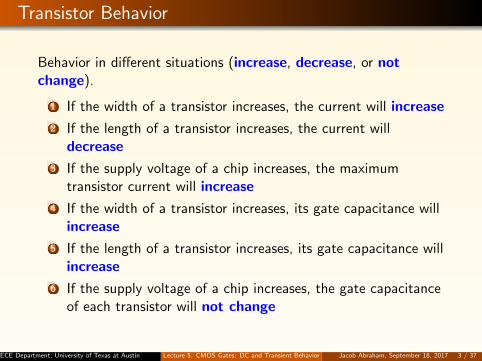
1 If the width of a transistor increases, the current will increase
2 If the length of a transistor increases, the current willdecrease
3 If the supply voltage of a chip increases, the maximumtransistor current will increase
4 If the width of a transistor increases, its gate capacitance willincrease
5 If the length of a transistor increases, its gate capacitance willincrease
6 If the supply voltage of a chip increases, the gate capacitanceof each transistor will not change
ECE Department, University of Texas at Austin Lecture 5. CMOS Gates: DC and Transient Behavior Jacob Abraham, September 18, 2017 3 / 37
DC Response: Vout vs. Vin for a Gate
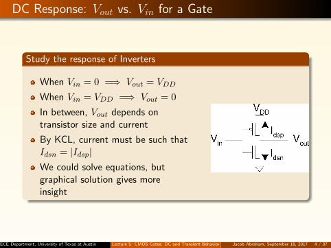
Study the response of Inverters
When Vin = 0 =⇒ Vout = VDD
When Vin = VDD =⇒ Vout = 0
In between, Vout depends ontransistor size and current
By KCL, current must be such thatIdsn = |Idsp|We could solve equations, butgraphical solution gives moreinsight
ECE Department, University of Texas at Austin Lecture 5. CMOS Gates: DC and Transient Behavior Jacob Abraham, September 18, 2017 4 / 37

Transistor Operation
Current through transistor depends on the region of operation
Need to identify for what Vin and Vout are nMOS and pMOSin Cutoff, Linear or Saturation
nMOS Operation
Cutoff Linear Saturated
Vgsn < Vtn Vgsn > Vtn Vgsn > VtnVin < Vtn Vin > Vtn Vin > Vtn
Vdsn < Vgsn − Vtn Vdsn > Vgsn − VtnVout < Vin − Vtn Vout > Vin − Vtn
Vgsn = Vin
Vdsn = Vout
ECE Department, University of Texas at Austin Lecture 5. CMOS Gates: DC and Transient Behavior Jacob Abraham, September 18, 2017 5 / 37
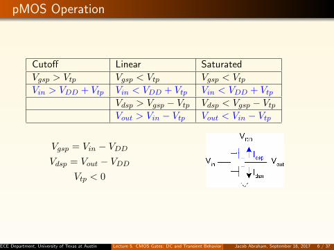
pMOS Operation
Cutoff Linear Saturated
Vgsp > Vtp Vgsp < Vtp Vgsp < VtpVin > VDD + Vtp Vin < VDD + Vtp Vin < VDD + Vtp
Vdsp > Vgsp − Vtp Vdsp < Vgsp − VtpVout > Vin − Vtp Vout < Vin − Vtp
Vgsp = Vin − VDDVdsp = Vout − VDD
Vtp < 0
ECE Department, University of Texas at Austin Lecture 5. CMOS Gates: DC and Transient Behavior Jacob Abraham, September 18, 2017 6 / 37
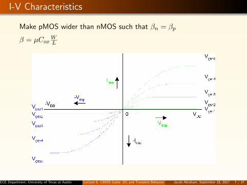
I-V Characteristics
Make pMOS wider than nMOS such that βn = βp
β = µCoxWL
ECE Department, University of Texas at Austin Lecture 5. CMOS Gates: DC and Transient Behavior Jacob Abraham, September 18, 2017 7 / 37
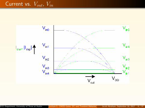
Current vs. Vout, Vin
ECE Department, University of Texas at Austin Lecture 5. CMOS Gates: DC and Transient Behavior Jacob Abraham, September 18, 2017 8 / 37
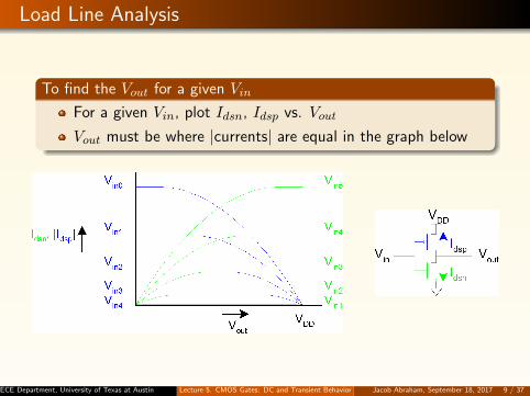
Load Line Analysis
To find the Vout for a given Vin
For a given Vin, plot Idsn, Idsp vs. Vout
Vout must be where |currents| are equal in the graph below
ECE Department, University of Texas at Austin Lecture 5. CMOS Gates: DC and Transient Behavior Jacob Abraham, September 18, 2017 9 / 37

DC Transfer Curve
Transcribe points on to Vin vs. Vout plot
ECE Department, University of Texas at Austin Lecture 5. CMOS Gates: DC and Transient Behavior Jacob Abraham, September 18, 2017 10 / 37
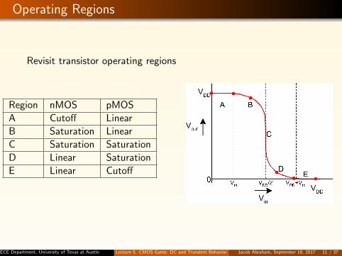
Operating Regions
Revisit transistor operating regions
Region nMOS pMOS
A Cutoff Linear
B Saturation Linear
C Saturation Saturation
D Linear Saturation
E Linear Cutoff
ECE Department, University of Texas at Austin Lecture 5. CMOS Gates: DC and Transient Behavior Jacob Abraham, September 18, 2017 11 / 37
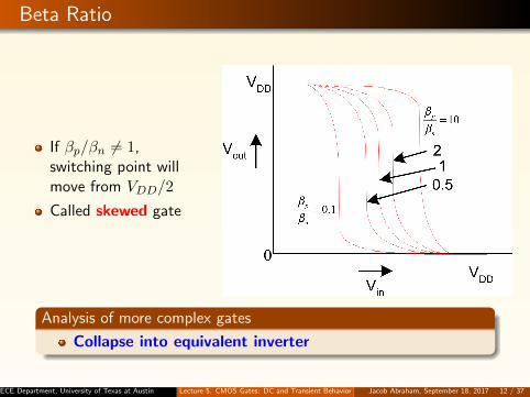
Beta Ratio
If βp/βn 6= 1,switching point willmove from VDD/2
Called skewed gate
Analysis of more complex gates
Collapse into equivalent inverter
ECE Department, University of Texas at Austin Lecture 5. CMOS Gates: DC and Transient Behavior Jacob Abraham, September 18, 2017 12 / 37
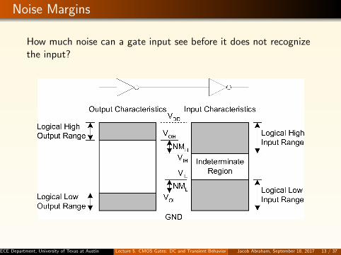
Noise Margins
How much noise can a gate input see before it does not recognizethe input?
ECE Department, University of Texas at Austin Lecture 5. CMOS Gates: DC and Transient Behavior Jacob Abraham, September 18, 2017 13 / 37
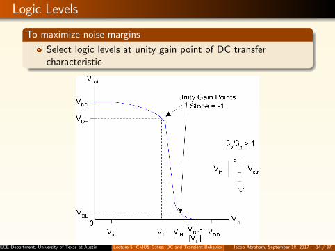
Logic Levels
To maximize noise margins
Select logic levels at unity gain point of DC transfercharacteristic
ECE Department, University of Texas at Austin Lecture 5. CMOS Gates: DC and Transient Behavior Jacob Abraham, September 18, 2017 14 / 37

Transient Response
DC analysis gives the Vout if Vin is constant
Transient analysis tells us Vout as Vin changes
Input is usually considered to be a step or ramp (from 0 toVDD or vice-versa)
ECE Department, University of Texas at Austin Lecture 5. CMOS Gates: DC and Transient Behavior Jacob Abraham, September 18, 2017 15 / 37
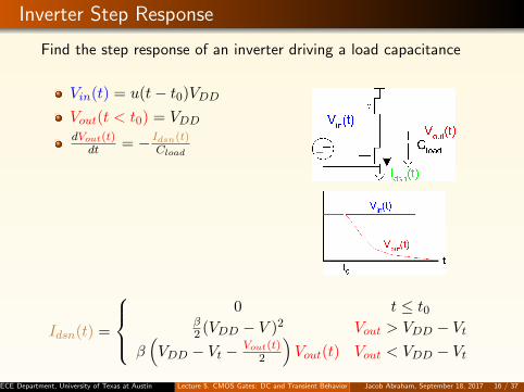
Inverter Step Response
Find the step response of an inverter driving a load capacitance
Vin(t) = u(t− t0)VDDVout(t < t0) = VDDdVout(t)
dt = − Idsn(t)Cload
Idsn(t) =
0 t ≤ t0
β2 (VDD − V )2 Vout > VDD − Vt
β(VDD − Vt − Vout(t)
2
)Vout(t) Vout < VDD − Vt
ECE Department, University of Texas at Austin Lecture 5. CMOS Gates: DC and Transient Behavior Jacob Abraham, September 18, 2017 16 / 37

Delay Definitions
tpdr: rising propagation delay
From input to rising output crossing VDD/2
tpdf : falling propagation delay
From input to falling output crossing VDD/2
tpd: average propagation delay
tpd = (tpdr + tpdf )/2
tr: rise time
From output crossing 0.2 VDD to 0.8 VDD
tf : fall time
From output crossing 0.8 VDD to 0.2 VDD
tcdr: rising contamination delay
Minimum time from input to rising output crossing VDD/2
tcdf : falling contamination delay
Minimum time from input to falling output crossing VDD/2
tcd: average contamination delay
tcd = (tcdr + tcdf )/2ECE Department, University of Texas at Austin Lecture 5. CMOS Gates: DC and Transient Behavior Jacob Abraham, September 18, 2017 17 / 37
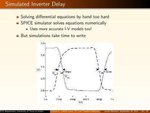
Simulated Inverter Delay
Solving differential equations by hand too hard
SPICE simulator solves equations numerically
Uses more accurate I-V models too!
But simulations take time to write
ECE Department, University of Texas at Austin Lecture 5. CMOS Gates: DC and Transient Behavior Jacob Abraham, September 18, 2017 18 / 37
Delay Estimation
We would like to be able to easily estimate delay
Not as accurate as simulationBut easier to ask “what if ...”?
The step response usually looks like a first order RC responsewith a decaying exponential
Use RC delay models to estimate delay
C = total capacitance on output nodeUse effective resistance RSo that tpd = RC
Characterize transistors by finding their effective R
Depends on average current as gate switches
ECE Department, University of Texas at Austin Lecture 5. CMOS Gates: DC and Transient Behavior Jacob Abraham, September 18, 2017 19 / 37

Example: Sizing 3-Input NAND Gate for Equal Rise andFall Times
Determine the transistor widths to achieve effective rise and fallresistances (times) equal to that of a unit inverter R
Annotate the 3-input NAND gate with gate and diffusioncapacitances
ECE Department, University of Texas at Austin Lecture 5. CMOS Gates: DC and Transient Behavior Jacob Abraham, September 18, 2017 20 / 37
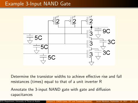
Example 3-Input NAND Gate
Determine the transistor widths to achieve effective rise and fallresistances (times) equal to that of a unit inverter R
Annotate the 3-input NAND gate with gate and diffusioncapacitances
ECE Department, University of Texas at Austin Lecture 5. CMOS Gates: DC and Transient Behavior Jacob Abraham, September 18, 2017 21 / 37
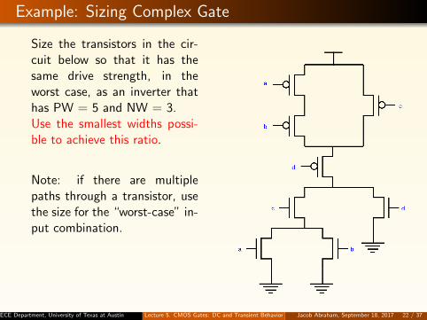
Example: Sizing Complex Gate
Size the transistors in the cir-cuit below so that it has thesame drive strength, in theworst case, as an inverter thathas PW = 5 and NW = 3.Use the smallest widths possi-ble to achieve this ratio.
Note: if there are multiplepaths through a transistor, usethe size for the “worst-case” in-put combination.
ECE Department, University of Texas at Austin Lecture 5. CMOS Gates: DC and Transient Behavior Jacob Abraham, September 18, 2017 22 / 37
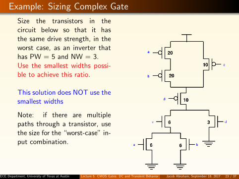
Example: Sizing Complex Gate
Size the transistors in thecircuit below so that it hasthe same drive strength, in theworst case, as an inverter thathas PW = 5 and NW = 3.Use the smallest widths possi-ble to achieve this ratio.
This solution does NOT use thesmallest widths
Note: if there are multiplepaths through a transistor, usethe size for the “worst-case” in-put combination.
ECE Department, University of Texas at Austin Lecture 5. CMOS Gates: DC and Transient Behavior Jacob Abraham, September 18, 2017 23 / 37

Example: Sizing of Complex Gate – Better Solution
Size the transistors in thecircuit below so that it hasthe same drive strength, in theworst case, as an inverter thathas PW = 5 and NW = 3.Use the smallest widths possi-ble to achieve this ratio.
Note: if there are multiplepaths through a transistor, usethe size for the “worst-case” in-put combination.
ECE Department, University of Texas at Austin Lecture 5. CMOS Gates: DC and Transient Behavior Jacob Abraham, September 18, 2017 24 / 37
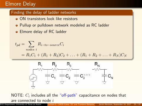
Elmore Delay
Finding the delay of ladder networks
ON transistors look like resistors
Pullup or pulldown network modeled as RC ladder
Elmore delay of RC ladder
tpd =∑
nodes i
Ri−to−sourceCi
= R1C1 + (R1 +R2)C2 + . . .+ (R1 +R2 + . . .+RN )CN
NOTE: Ci includes all the “off-path” capacitance on nodes thatare connected to node i
ECE Department, University of Texas at Austin Lecture 5. CMOS Gates: DC and Transient Behavior Jacob Abraham, September 18, 2017 25 / 37
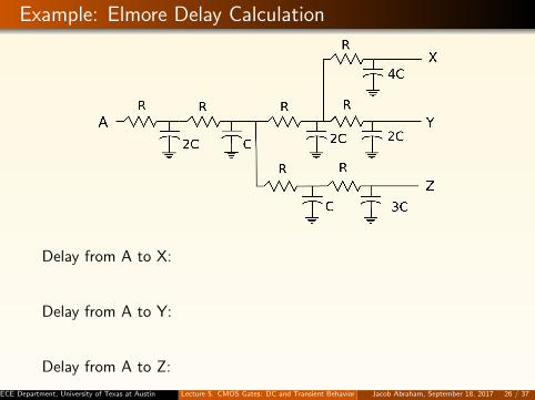
Example: Elmore Delay Calculation
Delay from A to X:
Delay from A to Y:
Delay from A to Z:
ECE Department, University of Texas at Austin Lecture 5. CMOS Gates: DC and Transient Behavior Jacob Abraham, September 18, 2017 26 / 37

Example: Elmore Delay Calculation, Cont’d
Delay from A to X: 40RC
Delay from A to Y: 38RC
Delay from A to Z: 35RC
ECE Department, University of Texas at Austin Lecture 5. CMOS Gates: DC and Transient Behavior Jacob Abraham, September 18, 2017 27 / 37
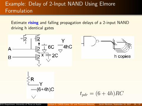
Example: Delay of 2-Input NAND Using ElmoreFormulation
Estimate rising and falling propagation delays of a 2-input NANDdriving h identical gates
tpdr = (6 + 4h)RC
ECE Department, University of Texas at Austin Lecture 5. CMOS Gates: DC and Transient Behavior Jacob Abraham, September 18, 2017 28 / 37

Example: Delay of 2-Input NAND Using ElmoreFormulation
Estimate rising and falling propagation delays of a 2-input NANDdriving h identical gates
tpdf = (2C)R
2+
[(6 + 4h)C
](R
2+R
2
)= (7 + 4h)RC
ECE Department, University of Texas at Austin Lecture 5. CMOS Gates: DC and Transient Behavior Jacob Abraham, September 18, 2017 29 / 37
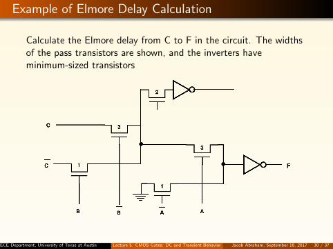
Example of Elmore Delay Calculation
Calculate the Elmore delay from C to F in the circuit. The widthsof the pass transistors are shown, and the inverters haveminimum-sized transistors
ECE Department, University of Texas at Austin Lecture 5. CMOS Gates: DC and Transient Behavior Jacob Abraham, September 18, 2017 30 / 37
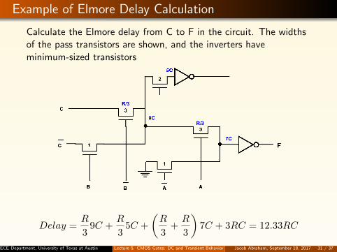
Example of Elmore Delay Calculation
Calculate the Elmore delay from C to F in the circuit. The widthsof the pass transistors are shown, and the inverters haveminimum-sized transistors
Delay =R
39C +
R
35C +
(R
3+R
3
)7C + 3RC = 12.33RC
ECE Department, University of Texas at Austin Lecture 5. CMOS Gates: DC and Transient Behavior Jacob Abraham, September 18, 2017 31 / 37
off-path
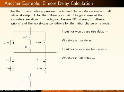
Another Example: Elmore Delay Calculation
Use the Elmore delay approximation to find the worst-case rise and falldelays at output F for the following circuit. The gate sizes of thetransistors are shown in the figure. Assume NO sharing of diffusionregions, and the worst-case conditions for the initial charge on a node.
Input for worst-case rise delay =
Worst-case rise delay =
Input for worst-case fall delay =
Worst-case fall delay =
ECE Department, University of Texas at Austin Lecture 5. CMOS Gates: DC and Transient Behavior Jacob Abraham, September 18, 2017 32 / 37
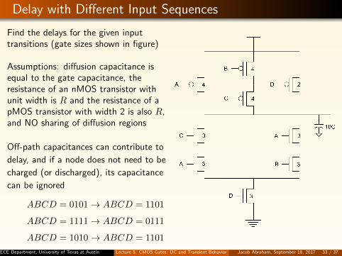
Delay with Different Input Sequences
Find the delays for the given inputtransitions (gate sizes shown in figure)
Assumptions: diffusion capacitance isequal to the gate capacitance, theresistance of an nMOS transistor withunit width is R and the resistance of apMOS transistor with width 2 is also R,and NO sharing of diffusion regions
Off-path capacitances can contribute to
delay, and if a node does not need to be
charged (or discharged), its capacitance
can be ignored
ABCD = 0101→ ABCD = 1101
ABCD = 1111→ ABCD = 0111
ABCD = 1010→ ABCD = 1101
ECE Department, University of Texas at Austin Lecture 5. CMOS Gates: DC and Transient Behavior Jacob Abraham, September 18, 2017 33 / 37

Delay with Different Input Sequence, Cont’d
Look at the charges on the nodesat the end of the first input of thesequence; only the capacitancesof the nodes which would changewith the second vector need to beconsidered
ABCD = 0101→ABCD = 1101;Delay = 36RC
ABCD = 1111→ABCD = 0111;Delay = 16RC
ABCD = 1010→ABCD = 1101;Delay = 43RC
ECE Department, University of Texas at Austin Lecture 5. CMOS Gates: DC and Transient Behavior Jacob Abraham, September 18, 2017 34 / 37

Delay Components
Delay has two parts
Parasitic Delay
6 or 7 RC
Independent of Load
Effort Delay
4h RC
Proportional to load capacitance
ECE Department, University of Texas at Austin Lecture 5. CMOS Gates: DC and Transient Behavior Jacob Abraham, September 18, 2017 35 / 37
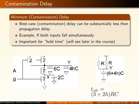
Contamination Delay
Minimum (Contamination) Delay
Best-case (contamination) delay can be substantially less thanpropagation delay
Example, If both inputs fall simultaneously
Important for “hold time” (will see later in the course)
tcdr =(3 + 2h)RC
ECE Department, University of Texas at Austin Lecture 5. CMOS Gates: DC and Transient Behavior Jacob Abraham, September 18, 2017 36 / 37
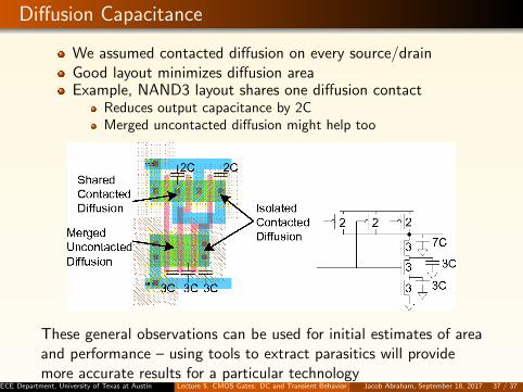
Diffusion Capacitance
We assumed contacted diffusion on every source/drainGood layout minimizes diffusion areaExample, NAND3 layout shares one diffusion contact
Reduces output capacitance by 2CMerged uncontacted diffusion might help too
These general observations can be used for initial estimates of areaand performance – using tools to extract parasitics will providemore accurate results for a particular technology
ECE Department, University of Texas at Austin Lecture 5. CMOS Gates: DC and Transient Behavior Jacob Abraham, September 18, 2017 37 / 37