Embed Size (px)
Citation preview
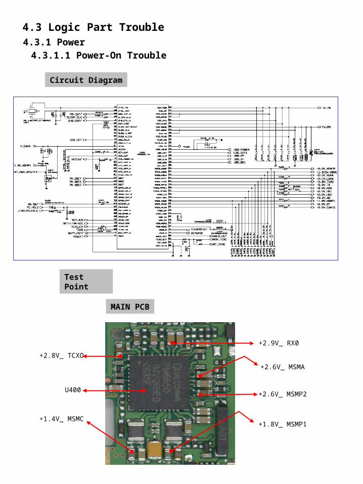
4.3.1 Power
Circuit Diagram
4.3.1.1 Power-On Trouble
4.3 Logic Part Trouble
Test Point
U400
+1.4V_ MSMC
+2.6V_ MSMP2
+1.8V_ MSMP1
+2.9V_ RX0
+2.8V_ TCXO
+2.6V_ MSMA
MAIN PCB

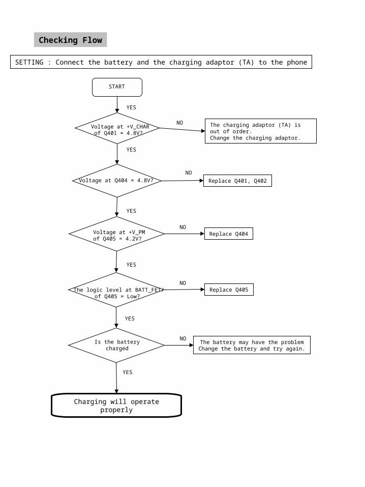
Checking Flow
START
YES
Check Battery Voltage> 3.4V ?
NOCharge of Change Battery and try again
Replace the U400
Re-download software & try again
The power-on procedure is completed.The problem may be elsewhere.
The Phone will power on. Replace the main board.
Check the contact of power-keyor dome switch
Push power-on key and check the level change of
U400 ON_SW/
Check the voltage Level of the following port at U400
+1.375V_MSMC +2.6V_MSMP2 +1.8V_MSMP1
+2.6V_MSMA +2.8V_TCXO
+2.9V_RX0
The logic level at PS_HOLD(R402) of U400 = High ?
Does it work properly?Does it work properly?
YES
YES
YES
YES
NO
NO
NO
NONO
YES

Circuit Diagram
4.3.1.2 Charging Trouble
Test Points Q404
+V_PM
Q405Q401
Q402
MAIN PCB
Checking Flow
SETTING : Connect the battery and the charging adaptor (TA) to the phone
START
YES
Voltage at +V_CHARof Q401 = 4.8V?
NO The charging adaptor (TA) is out of order.Change the charging adaptor.
Replace Q401, Q402Voltage at Q404 = 4.8V?
Voltage at +V_PMof Q405 = 4.2V?
YES
YES
YES
NO
NO
YES
Replace Q404
The logic level at BATT_FET/of Q405 = Low?
NOReplace Q405
Is the batterycharged
NOThe battery may have the problemChange the battery and try again.
Charging will operate properly
YES
MAIN PCB
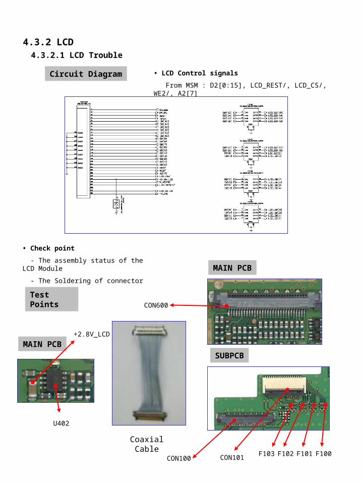
4.3.2 LCD
Circuit Diagram
4.3.2.1 LCD Trouble
Test Points
• LCD Control signals
From MSM : D2[0:15], LCD_REST/, LCD_CS/, WE2/, A2[7]
F100F101F102F103
CON600
U402
+2.8V_LCD
• Check point
- The assembly status of the LCD Module
- The Soldering of connector
Coaxial Cable
CON100 CON101
MAIN PCB
SUBPCB
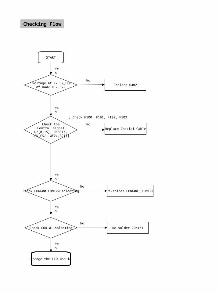
START
Voltage at +2.8V_LCDof U402 = 2.8V?
Check theControl signal
D2[0:15], RESET/,LCD_CS/, WE2/,A2[7]
No
No
Yes
Yes
Yes
Replace U402
Check CON600,CON100 soldering Re-solder CON600 ,CON100
Yes
Checking Flow
; Check F100, F101, F102, F103
Change the LCD Module
No
Yes
Check CON101 soldering Re-solder CON101
No
Replace Coaxial Cable

4.3.3 Camera
Circuit Diagram
4.3.3.1 Camera Trouble
• Camera Control signals
From MSM : CAM_DATA[0:7], CAM_RESET/, CAM_SDA, CAM_SCL,
CAM_CLK, CAM_PCLK

Test Points
F500
• Check point
- The assembly status of the Camera Module
- The Connection of connector
R536
X500
F501
CON502
U400
+2.6V_ CAMIO+2.6V_ CAMA
MAIN PCB
C519
R528
R529
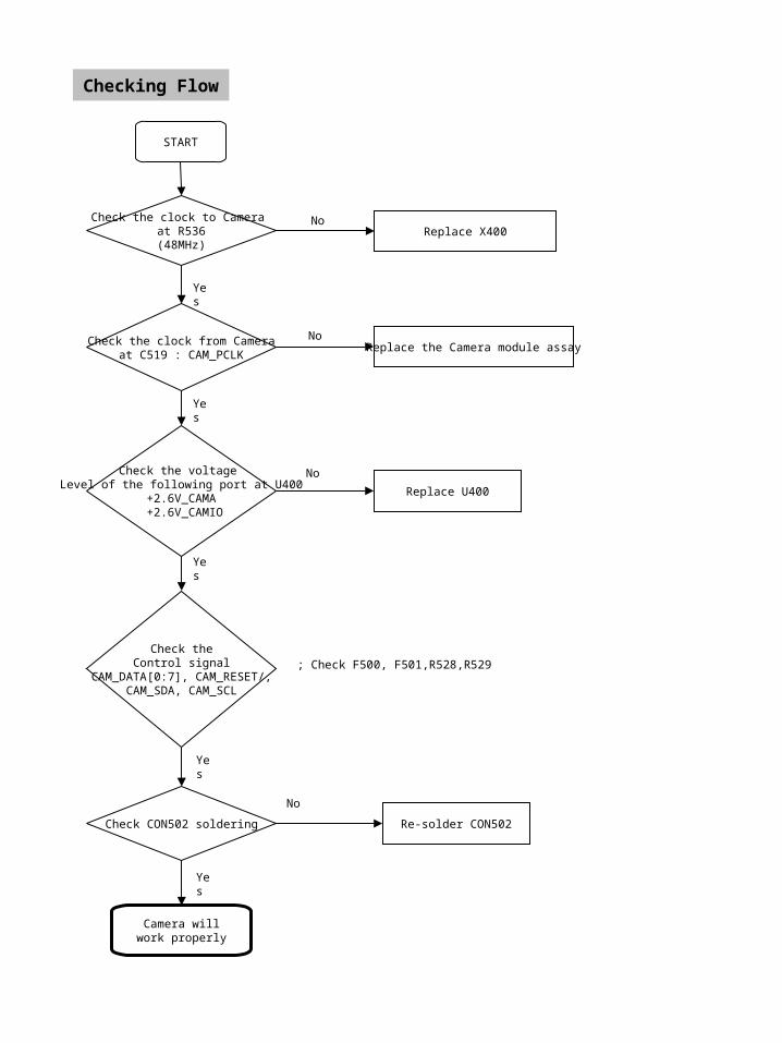
START
Check the clock to Camera at R536(48MHz)
Check the clock from Cameraat C519 : CAM_PCLK
Check theControl signal
CAM_DATA[0:7], CAM_RESET/,CAM_SDA, CAM_SCL
Camera willwork properly
Replace X400No
No
No
Yes
Yes
Yes
Replace the Camera module assay
Check CON502 soldering Re-solder CON502
Yes
Checking Flow
; Check F500, F501,R528,R529
Check the voltage Level of the following port at U400
+2.6V_CAMA +2.6V_CAMIO
No
Replace U400
Yes
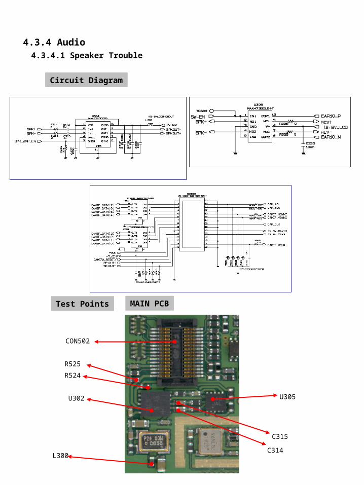
4.3.4 Audio
Circuit Diagram
4.3.4.1 Speaker Trouble
Test Points
U302
C315
L300C314
U305
R525
R524
CON502
MAIN PCB
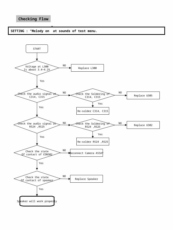
SETTING : “Melody on” at sounds of test menu.
Voltage at L300Is about 3.4~4.2V
START
Check the audio signal atC314, C315
Check the audio signal atR524 ,R525
Check the Soldering ofR524 ,R525
Check the stateOf contact of CON502
NO
NO
NO NO
Yes
Yes
Yes
Yes
Yes
Replace L300
Replace U302
Re-solder R524 ,R525
Check the Soldering ofC314, C315
NO
Yes
Replace U305
Re-solder C314, C315
Checking Flow
NOReconnect Camera ASSAY
Check the stateOf contact of speaker
Speaker will work properly
Yes
NOReplace Speaker
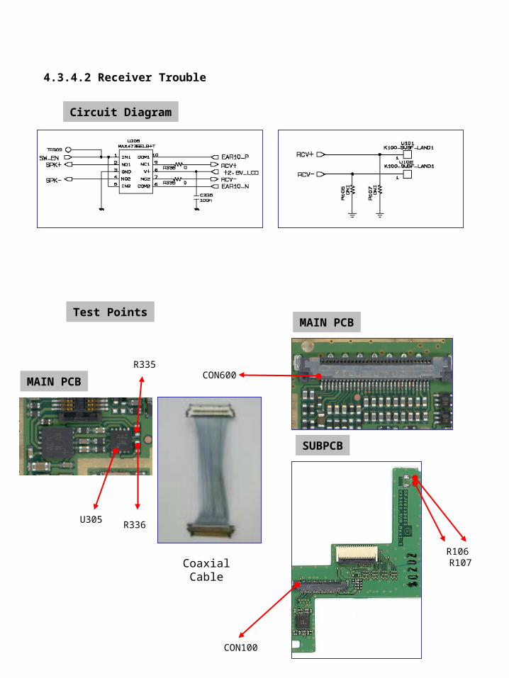
R106 R107
4.3.4.2 Receiver Trouble
Circuit Diagram
Test Points
CON600
Coaxial Cable
CON100
MAIN PCB
SUBPCB
U305
MAIN PCB
R336
R335
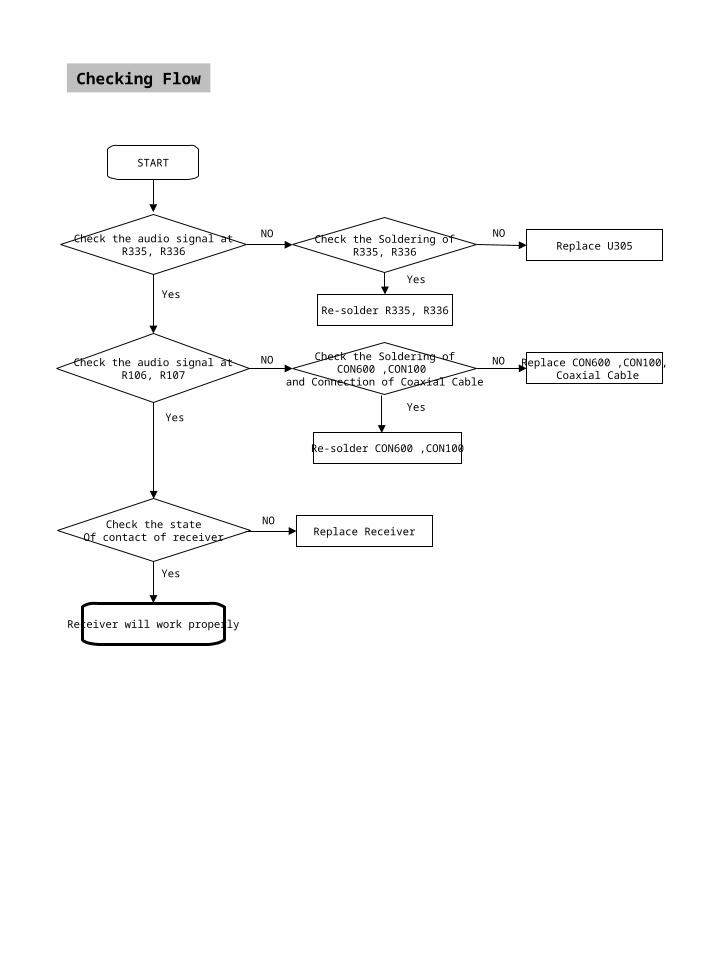
START
Check the audio signal atR335, R336
Check the audio signal atR106, R107
Check the Soldering ofCON600 ,CON100
and Connection of Coaxial Cable
Check the stateOf contact of receiver
Receiver will work properly
NO
NO NO
Yes
Yes
Yes
Yes
Replace CON600 ,CON100, Coaxial Cable
Re-solder CON600 ,CON100
Check the Soldering ofR335, R336
NO
Yes
Replace U305
Re-solder R335, R336
Checking Flow
NOReplace Receiver

MAIN PCB
4.3.4.4 Headset Trouble
Circuit Diagram
Test Points
U303
R331CON604
U304R338
R339
MAIN PCB
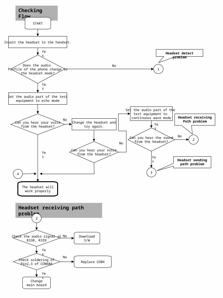
Checking Flow
START
Does the audio Profile of the phone change to
the headset mode?
Can you hear your voicefrom the headset?
The headset willwork properly
Insert the headset to the handset.
Change the headset andtry again.
No
No
Yes
Yes
Set the audio part of the testequipment to echo mode
Headset detect problem
Can you hear your voicefrom the headset?
Set the audio part of the test equipment to
continuous wave mode Headset receivingPath problem
Can you hear the soundfrom the headset?
Headset sending path problem
1
4
2
3
No
Yes
No
Headset receiving path problem
2
Check the audio signal atR338, R339
Check soldering ofPin2,3 of CON604
Changemain board
DownloadS/W
Replace U304
Yes
Yes
No
No
Yes
Yes
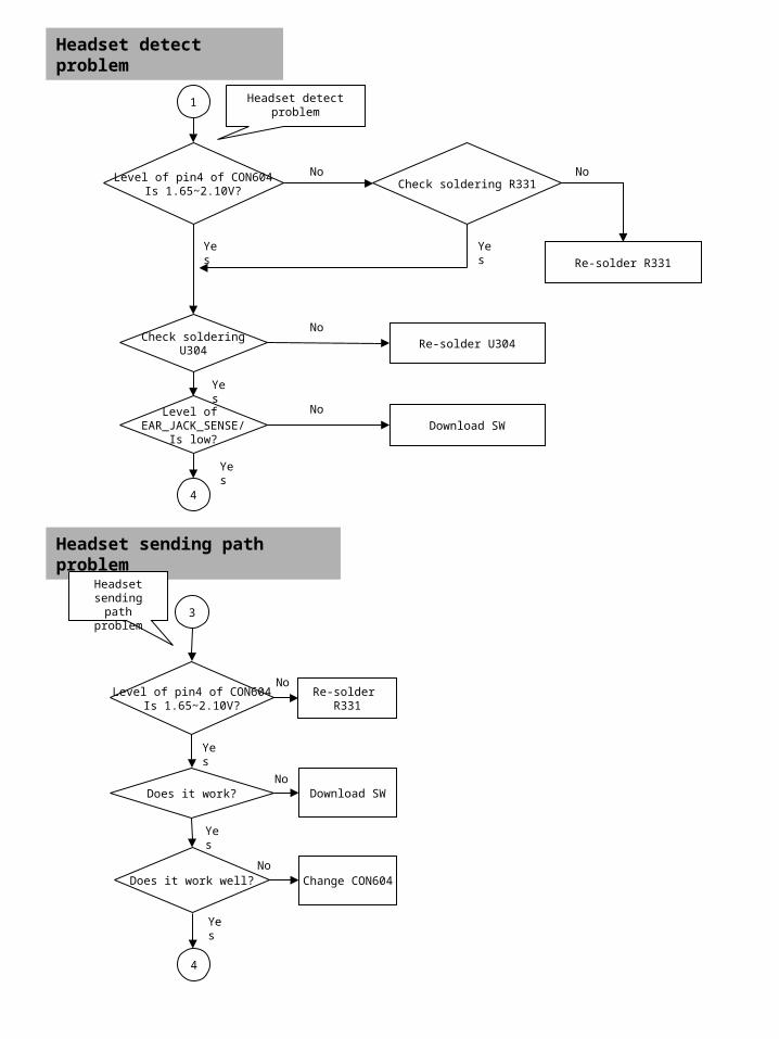
Headset detect problem
Level of pin4 of CON604Is 1.65~2.10V?
Re-solder R331
No
Yes
1
Check soldering R331
Check solderingU304
Level of EAR_JACK_SENSE/
Is low?
Re-solder U304
Download SW
4
No
Headset sending path problem
Headset detectproblem
Headset sending
path problem 3
Level of pin4 of CON604Is 1.65~2.10V?
Does it work?
Re-solder R331
Download SW
Does it work well?
4
Change CON604
No
No
Yes
Yes
Yes
No
No
No
Yes
Yes
Yes
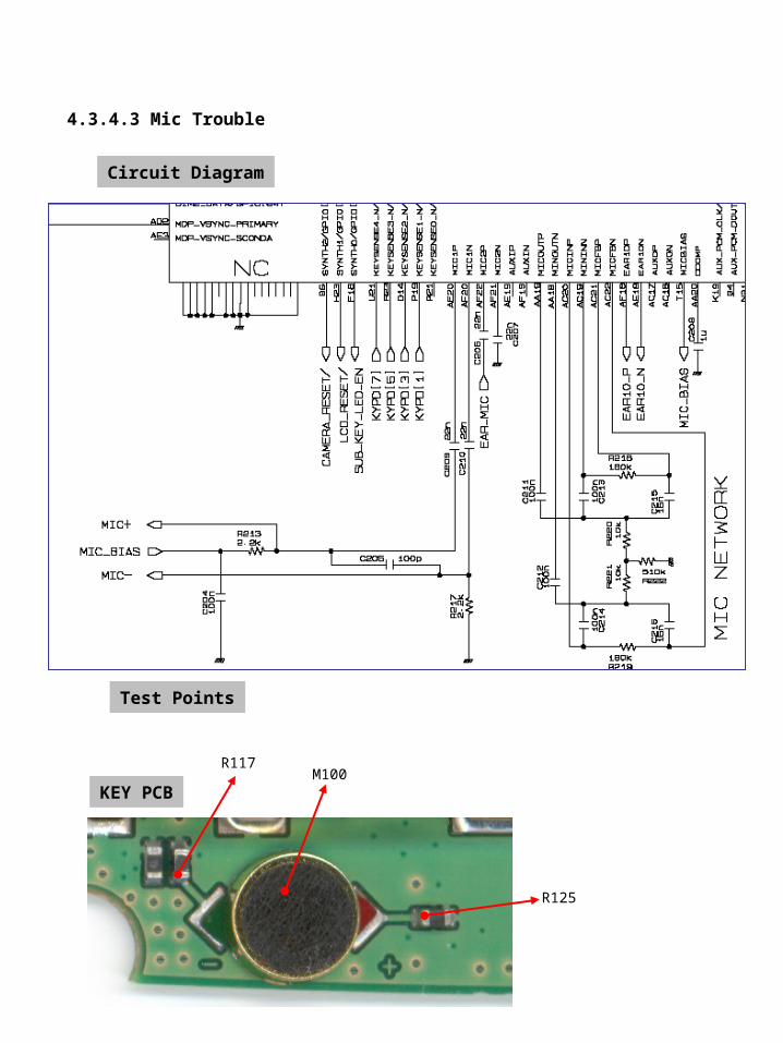
4.3.4.3 Mic Trouble
Circuit Diagram
Test Points
M100R117
R125
KEY PCB
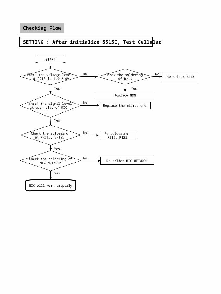
SETTING : After initialize 5515C, Test Cellular
START
Check the voltage level at R213 is 1.0~2.0V
Check the soldering Of R213
Re-solder R213
Replace MSM
Check the signal levelat each side of MIC.
Replace the microphone
Check the soldering at VR117, VR125
Check the soldering ofMIC NETWORK
Re-solder MIC NETWORK
MIC will work properly
Checking Flow
Yes
Yes
Yes
Yes
No No
No
No
No
Yes
Re-soldering R117, R125
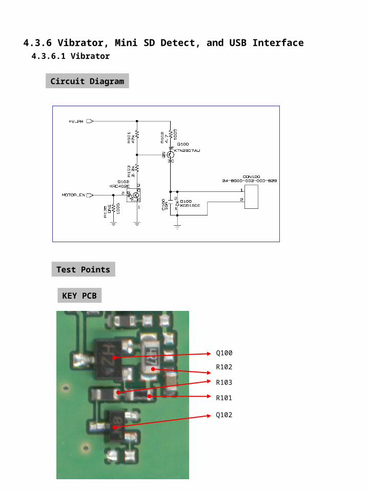
4.3.6 Vibrator, Mini SD Detect, and USB Interface
Circuit Diagram
4.3.6.1 Vibrator
Test Points
R103
Q100
R101
KEY PCB
R102
Q102
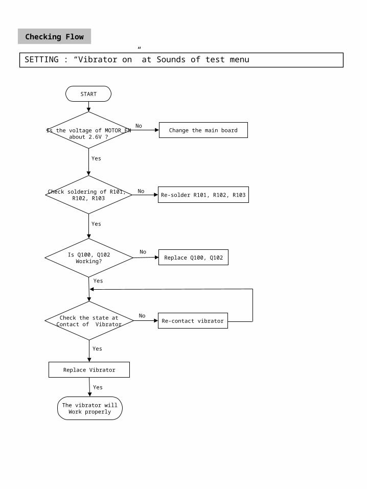
Checking Flow
SETTING : “Vibrator on” at Sounds of test menu
START
Is the voltage of MOTOR_ENabout 2.6V ?
Change the main board
Check soldering of R101, R102, R103
Re-solder R101, R102, R103
Check the state atContact of Vibrator
Re-contact vibrator
Replace Vibrator
The vibrator willWork properly
No
No
No
Yes
Yes
Yes
Yes
Is Q100, Q102Working?
Replace Q100, Q102No
Yes
Circuit Diagram
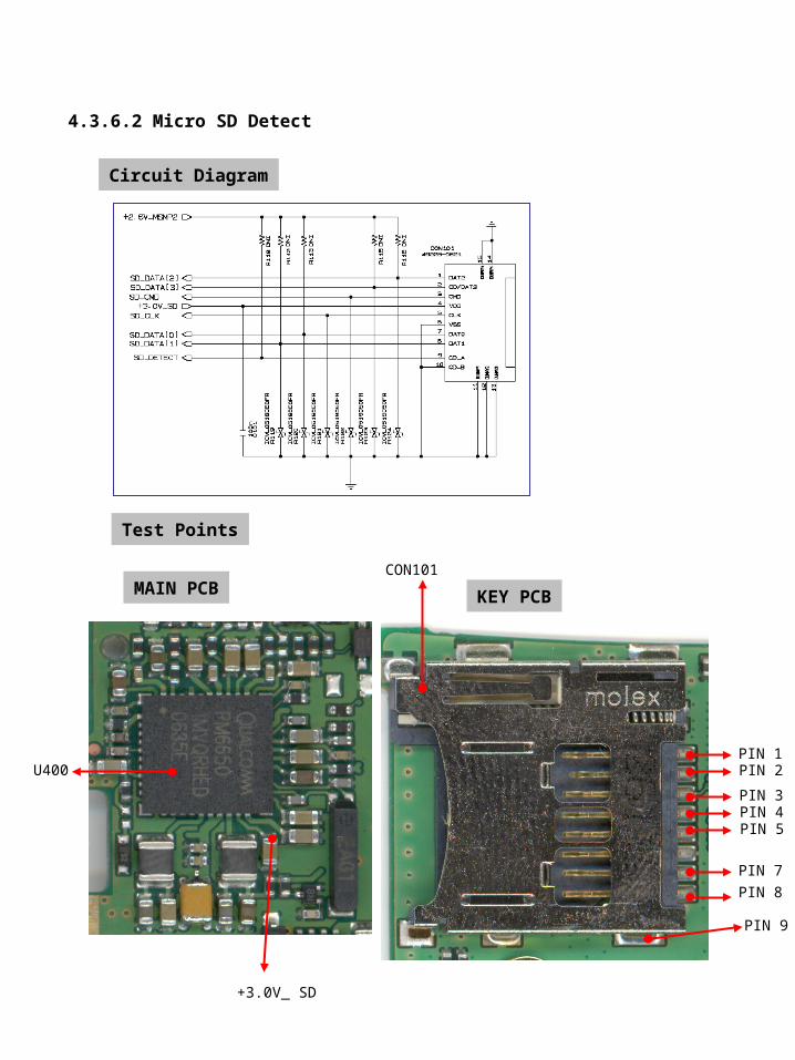
4.3.6.2 Micro SD Detect
Test Points
CON101
PIN 1PIN 2
PIN 3PIN 4PIN 5
PIN 7
PIN 8
PIN 9
U400
+3.0V_ SD
MAIN PCB KEY PCB
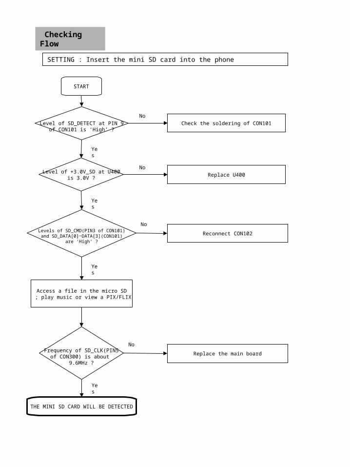
Checking Flow
START
Level of SD_DETECT at PIN 9of CON101 is ‘High’ ?
Level of +3.0V_SD at U400is 3.0V ?
Levels of SD_CMD(PIN3 of CON101)and SD_DATA[0]~DATA[3](CON101)
are ‘High’ ?
THE MINI SD CARD WILL BE DETECTED
Check the soldering of CON101
Replace U400
No
No
No
Yes
Yes
Yes
Frequency of SD_CLK(PIN5of CON300) is about
9.6MHz ?
Yes
No
SETTING : Insert the mini SD card into the phone
Reconnect CON102
Access a file in the micro SD ; play music or view a PIX/FLIX
Replace the main board
Circuit Diagram
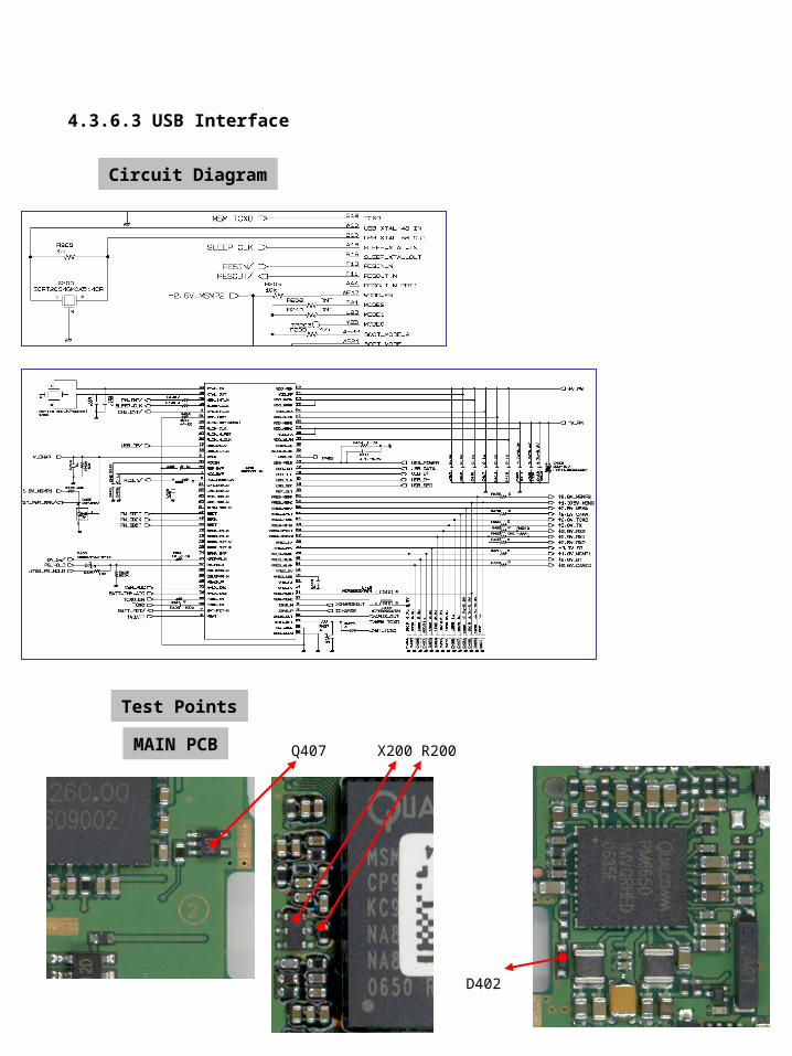
4.3.6.3 USB Interface
Test Points
D402
MAIN PCB Q407 X200 R200
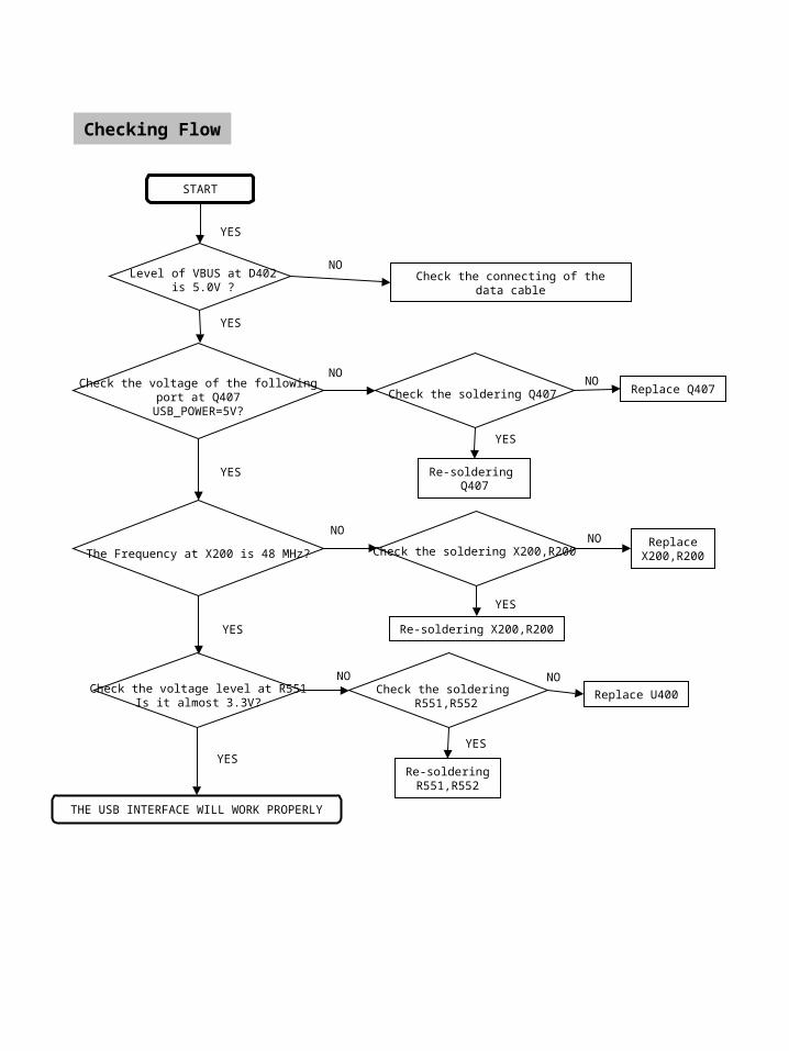
Checking Flow
START
YES
Level of VBUS at D402is 5.0V ?
NOCheck the connecting of the data cable
Check the voltage of the followingport at Q407
USB_POWER=5V?
YES
NO
YES
Check the soldering Q407 Replace Q407
Re-soldering Q407
Check the voltage level at R551Is it almost 3.3V?
YES
NOCheck the soldering
R551,R552Replace U400
Re-solderingR551,R552
THE USB INTERFACE WILL WORK PROPERLY
The Frequency at X200 is 48 MHz?
YES
NO
Check the soldering X200,R200Replace
X200,R200
Re-soldering X200,R200
NO
NO
YES
YES
NO
YES