Embed Size (px)
Citation preview

TPIC44H014-CHANNEL SERIAL AND PARALLEL HIGH-SIDE PRE-FET DRIVER
SLIS088 – SEPTEMBER 1998
1POST OFFICE BOX 655303 • DALLAS, TEXAS 75265
Serial or Parallel Control of Gate Outputs
Sleep State for Low Quiescent Current
Independent On-State SourceShort-to-Ground (Shorted-Load)Detection/Protection
Independent On-State Over-CurrentDetection/Protection With Dynamic FaultThreshold
Independent Off-State Open-LoadDetection
Supply Over-Voltage Lockout Protection
Asynchronous Open-Drain Fault InterruptTerminal to Flag Fault Conditions. OutputCan be OR’ed With Multiple Devices
Encoded Fault Status Reporting ThroughSerial Output Terminal (2-Bits Per Channel)
Programmable On-State Fault DeglitchTimers
High Impedance CMOS Compatible InputsWith Hysteresis
Fault Mode Selection: Outputs Latched Offor Switched at Low Duty Cycle
Device Can be Cascaded With SerialInterface
description
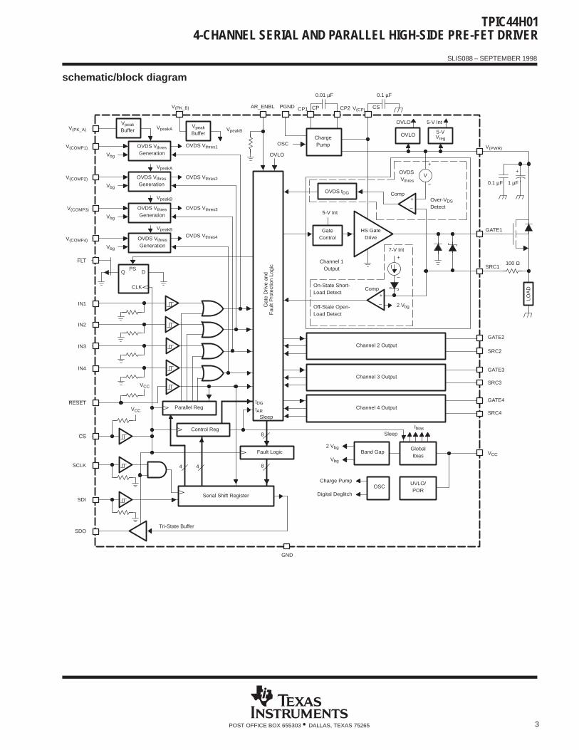
The TPIC44H01 is a four channel high-side pre-FET driver which provides serial or parallel input interface tocontrol four external NMOS power FETs. It is designed for use in low frequency switching applications forresistive or inductive loads, including solenoids and incandescent bulbs.
Each channel has over-current, short-to-ground, and open-load detection that is flagged through the FLT pinand distinguished through the serial interface. Over-current thresholds are set through the V(PK_x) andV(COMP1-4) pins. Short-to-ground and open-load thresholds are set internally to approximately 2.5 V. TheAR_ENBL pin is used to define the operation of the device during a fault condition, allowing the outputs to eitherlatch off or to enter a low duty cycle, auto-retry mode. An over-voltage lockout circuit on V(PWR) protects thedevice and the external FETs. A low current sleep state mode is provided to allow the TPIC44H01 to be usedin applications where V(PWR) is connected directly to the battery. An internal charge pump allows the use ofN-channel FETs for high-side drive applications, while current-limit gate drive provides slope control for reducedRFI.
By having the unique ability to develop a dynamic over-current threshold, the TPIC44H01 can be used to driveincandescent bulbs with long inrush currents without falsely flagging a fault. Likewise, the user can select aninternally set over-current threshold of ~1.25 V by pulling the respective V(COMP1-4) pin to VCC.
Copyright 1998, Texas Instruments IncorporatedPRODUCTION DATA information is current as of publication date.Products conform to specifications per the terms of Texas Instrumentsstandard warranty. Production processing does not necessarily includetesting of all parameters.
Please be aware that an important notice concerning availability, standard warranty, and use in critical applications ofTexas Instruments semiconductor products and disclaimers thereto appears at the end of this data sheet.
TI is a trademark of Texas Instruments Incorporated.
1
2
3
4
5
6
78
9
10
11
12
13
14
15
16
32
31
30
29
28
27
2625
24
23
22
21
20
19
18
17
CSSD0SDI
SCLKAR_ENBL
GNDIN1IN2IN3IN4
VCCV(PK_A)V(PK_B)
V(COMP1)V(COMP2)V(COMP3)
PGNDV(PWR)CP1CP2V(CP)GATE1SRC1GATE2SRC2GATE3SRC3GATE4SRC4FLTRESETV(COMP4)
DA PACKAGE(TOP VIEW)
TPIC44H014-CHANNEL SERIAL AND PARALLEL HIGH-SIDE PRE-FET DRIVER
SLIS088 – SEPTEMBER 1998
2 POST OFFICE BOX 655303 • DALLAS, TEXAS 75265
description (continued)
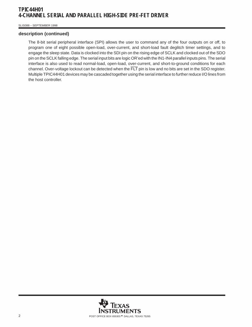
The 8-bit serial peripheral interface (SPI) allows the user to command any of the four outputs on or off, toprogram one of eight possible open-load, over-current, and short-load fault deglitch timer settings, and toengage the sleep state. Data is clocked into the SDI pin on the rising edge of SCLK and clocked out of the SDOpin on the SCLK falling edge. The serial input bits are logic OR’ed with the IN1-IN4 parallel inputs pins. The serialinterface is also used to read normal-load, open-load, over-current, and short-to-ground conditions for eachchannel. Over-voltage lockout can be detected when the FLT pin is low and no bits are set in the SDO register.Multiple TPIC44H01 devices may be cascaded together using the serial interface to further reduce I/O lines fromthe host controller.
TPIC44H014-CHANNEL SERIAL AND PARALLEL HIGH-SIDE PRE-FET DRIVER
SLIS088 – SEPTEMBER 1998
3POST OFFICE BOX 655303 • DALLAS, TEXAS 75265
schematic/block diagram
V
VpeakBufferV(PK_A)
OVDS VthresGeneration
OVDS VthresGeneration
V(COMP1)
Vbg
V(COMP2)
Vbg
OVDS Vthres1
OVDS Vthres2
VpeakA
VpeakA
OVDS VthresGeneration
V(COMP3)
Vbg
OVDS Vthres3
VpeakB
OVDS VthresGeneration
V(COMP4)
Vbg
OVDS Vthres4
VpeakB
Q D
CLK
PS
FLT
IN1
IN2
IN3
IN4
VCC
RESET
VpeakBuffer
VpeakB
V(PK_B)
Parallel Reg
Control Reg
VCC
CS
Sleep
tDG
Gat
e D
rive
and
Fau
lt P
rote
ctio
n Lo
gic
AR_ENBL
OVLO
ChargePump
0.01 µF
CP
0.1 µF
CSPGND CP1 CP2 V(CP)
OVLO
OSC
5-VVreg
OVLO 5-V Int
+
–
OVDSVthres
+
–
OVDS tDG CompOver-VDSDetect
HS GateDrive
GateControl
+
–
7-V Int
+
–
Comp
I
5-V Int
2 Vbg
On-State Short-Load Detect
Off-State Open-Load Detect
Channel 1Output
Channel 2 Output
Channel 3 Output
Channel 4 Output
GATE2
SRC2
GATE3
SRC3
GATE4
SRC4
GlobalIbias
Band Gap
IbiasSleep8
Fault Logic
Serial Shift Register
4 4SCLK
SDI
SDOTri-State Buffer
2 Vbg
Vbg
UVLO/POR
OSCCharge Pump
Digital Deglitch
VCC
0.1 µF 1 µF
+
LOA
D
100 ΩSRC1
GATE1
V(PWR)
8
tAR
GND
TPIC44H014-CHANNEL SERIAL AND PARALLEL HIGH-SIDE PRE-FET DRIVER
SLIS088 – SEPTEMBER 1998
4 POST OFFICE BOX 655303 • DALLAS, TEXAS 75265
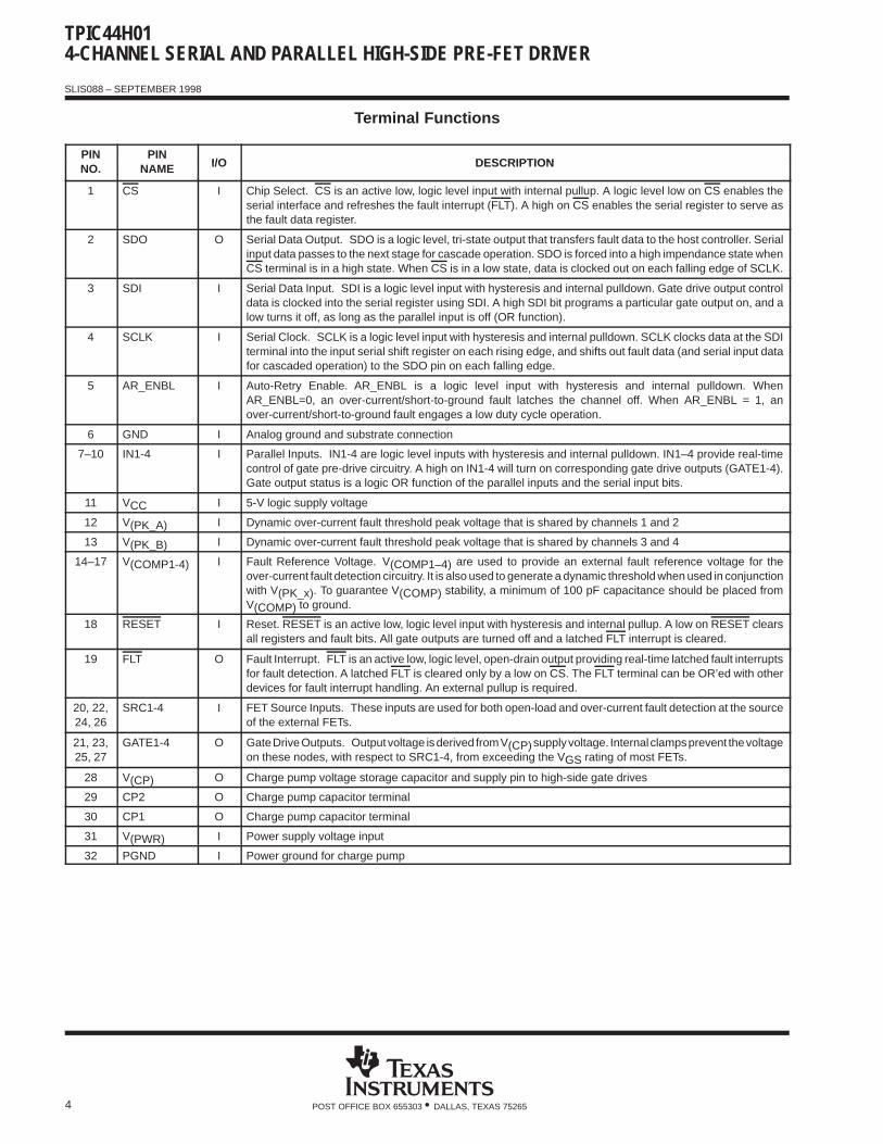
Terminal Functions
PIN PINI/O DESCRIPTIONNO. NAME I/O DESCRIPTION
1 CS I Chip Select. CS is an active low, logic level input with internal pullup. A logic level low on CS enables theserial interface and refreshes the fault interrupt (FLT). A high on CS enables the serial register to serve asthe fault data register.
2 SDO O Serial Data Output. SDO is a logic level, tri-state output that transfers fault data to the host controller. Serialinput data passes to the next stage for cascade operation. SDO is forced into a high impendance state whenCS terminal is in a high state. When CS is in a low state, data is clocked out on each falling edge of SCLK.
3 SDI I Serial Data Input. SDI is a logic level input with hysteresis and internal pulldown. Gate drive output controldata is clocked into the serial register using SDI. A high SDI bit programs a particular gate output on, and alow turns it off, as long as the parallel input is off (OR function).
4 SCLK I Serial Clock. SCLK is a logic level input with hysteresis and internal pulldown. SCLK clocks data at the SDIterminal into the input serial shift register on each rising edge, and shifts out fault data (and serial input datafor cascaded operation) to the SDO pin on each falling edge.
5 AR_ENBL I Auto-Retry Enable. AR_ENBL is a logic level input with hysteresis and internal pulldown. WhenAR_ENBL=0, an over-current/short-to-ground fault latches the channel off. When AR_ENBL = 1, anover-current/short-to-ground fault engages a low duty cycle operation.
6 GND I Analog ground and substrate connection
7–10 IN1-4 I Parallel Inputs. IN1-4 are logic level inputs with hysteresis and internal pulldown. IN1–4 provide real-timecontrol of gate pre-drive circuitry. A high on IN1-4 will turn on corresponding gate drive outputs (GATE1-4).Gate output status is a logic OR function of the parallel inputs and the serial input bits.
11 VCC I 5-V logic supply voltage
12 V(PK_A) I Dynamic over-current fault threshold peak voltage that is shared by channels 1 and 2
13 V(PK_B) I Dynamic over-current fault threshold peak voltage that is shared by channels 3 and 4
14–17 V(COMP1-4) I Fault Reference Voltage. V(COMP1–4) are used to provide an external fault reference voltage for theover-current fault detection circuitry. It is also used to generate a dynamic threshold when used in conjunctionwith V(PK_x). To guarantee V(COMP) stability, a minimum of 100 pF capacitance should be placed fromV(COMP) to ground.
18 RESET I Reset. RESET is an active low, logic level input with hysteresis and internal pullup. A low on RESET clearsall registers and fault bits. All gate outputs are turned off and a latched FLT interrupt is cleared.
19 FLT O Fault Interrupt. FLT is an active low, logic level, open-drain output providing real-time latched fault interruptsfor fault detection. A latched FLT is cleared only by a low on CS. The FLT terminal can be OR’ed with otherdevices for fault interrupt handling. An external pullup is required.
20, 22,24, 26
SRC1-4 I FET Source Inputs. These inputs are used for both open-load and over-current fault detection at the sourceof the external FETs.
21, 23,25, 27
GATE1-4 O Gate Drive Outputs. Output voltage is derived from V(CP) supply voltage. Internal clamps prevent the voltageon these nodes, with respect to SRC1-4, from exceeding the VGS rating of most FETs.
28 V(CP) O Charge pump voltage storage capacitor and supply pin to high-side gate drives
29 CP2 O Charge pump capacitor terminal
30 CP1 O Charge pump capacitor terminal
31 V(PWR) I Power supply voltage input
32 PGND I Power ground for charge pump
TPIC44H014-CHANNEL SERIAL AND PARALLEL HIGH-SIDE PRE-FET DRIVER
SLIS088 – SEPTEMBER 1998
5POST OFFICE BOX 655303 • DALLAS, TEXAS 75265
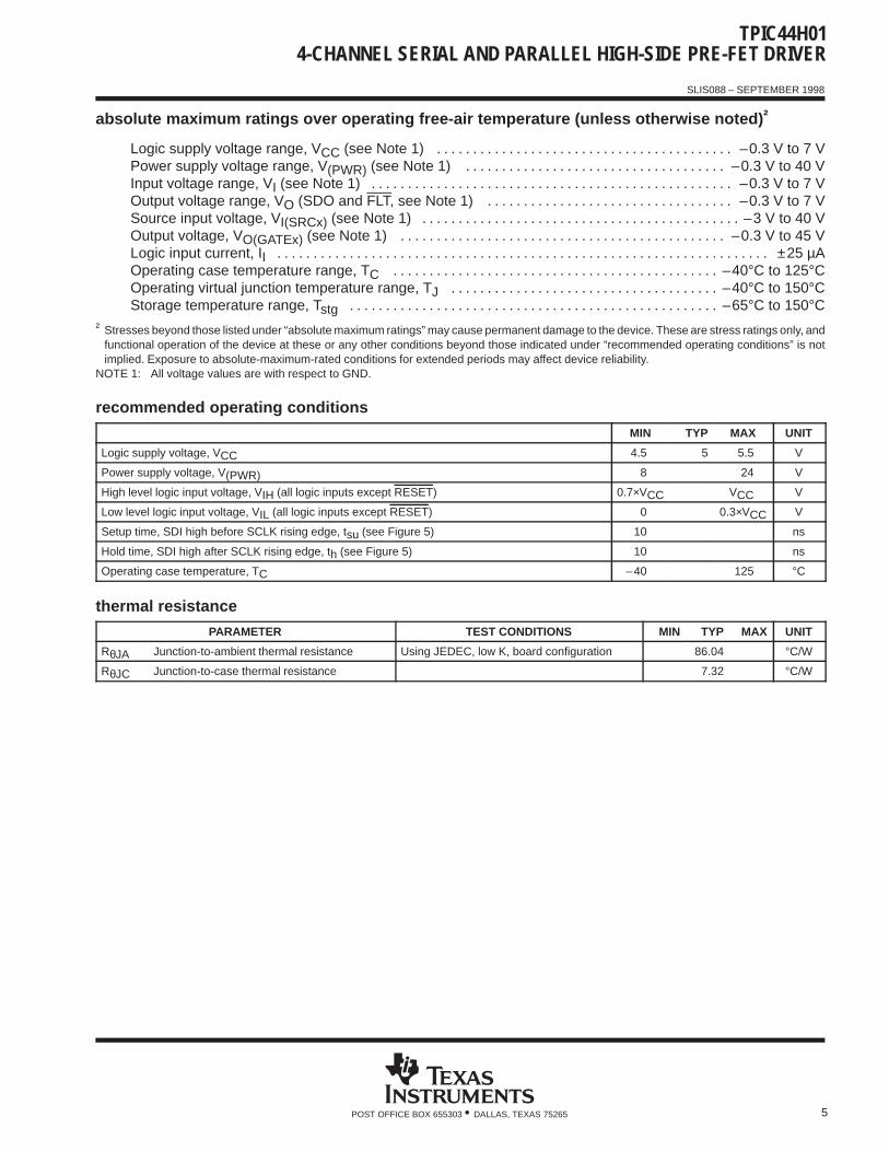
absolute maximum ratings over operating free-air temperature (unless otherwise noted) †
Logic supply voltage range, VCC (see Note 1) –0.3 V to 7 V. . . . . . . . . . . . . . . . . . . . . . . . . . . . . . . . . . . . . . . . . Power supply voltage range, V(PWR) (see Note 1) –0.3 V to 40 V. . . . . . . . . . . . . . . . . . . . . . . . . . . . . . . . . . . . Input voltage range, VI (see Note 1) –0.3 V to 7 V. . . . . . . . . . . . . . . . . . . . . . . . . . . . . . . . . . . . . . . . . . . . . . . . . . Output voltage range, VO (SDO and FLT, see Note 1) –0.3 V to 7 V. . . . . . . . . . . . . . . . . . . . . . . . . . . . . . . . . . Source input voltage, VI(SRCx) (see Note 1) –3 V to 40 V. . . . . . . . . . . . . . . . . . . . . . . . . . . . . . . . . . . . . . . . . . . . Output voltage, VO(GATEx) (see Note 1) –0.3 V to 45 V. . . . . . . . . . . . . . . . . . . . . . . . . . . . . . . . . . . . . . . . . . . . . Logic input current, II ±25 µA. . . . . . . . . . . . . . . . . . . . . . . . . . . . . . . . . . . . . . . . . . . . . . . . . . . . . . . . . . . . . . . . . . . . Operating case temperature range, TC –40°C to 125°C. . . . . . . . . . . . . . . . . . . . . . . . . . . . . . . . . . . . . . . . . . . . . Operating virtual junction temperature range, TJ –40°C to 150°C. . . . . . . . . . . . . . . . . . . . . . . . . . . . . . . . . . . . . Storage temperature range, Tstg –65°C to 150°C. . . . . . . . . . . . . . . . . . . . . . . . . . . . . . . . . . . . . . . . . . . . . . . . . . .
† Stresses beyond those listed under “absolute maximum ratings” may cause permanent damage to the device. These are stress ratings only, andfunctional operation of the device at these or any other conditions beyond those indicated under “recommended operating conditions” is notimplied. Exposure to absolute-maximum-rated conditions for extended periods may affect device reliability.
NOTE 1: All voltage values are with respect to GND.
recommended operating conditions
MIN TYP MAX UNIT
Logic supply voltage, VCC 4.5 5 5.5 V
Power supply voltage, V(PWR) 8 24 V
High level logic input voltage, VIH (all logic inputs except RESET) 0.7×VCC VCC V
Low level logic input voltage, VIL (all logic inputs except RESET) 0 0.3×VCC V
Setup time, SDI high before SCLK rising edge, tsu (see Figure 5) 10 ns
Hold time, SDI high after SCLK rising edge, th (see Figure 5) 10 ns
Operating case temperature, TC –40 125 °C
thermal resistance
PARAMETER TEST CONDITIONS MIN TYP MAX UNIT
RθJA Junction-to-ambient thermal resistance Using JEDEC, low K, board configuration 86.04 °C/W
RθJC Junction-to-case thermal resistance 7.32 °C/W
TPIC44H014-CHANNEL SERIAL AND PARALLEL HIGH-SIDE PRE-FET DRIVER
SLIS088 – SEPTEMBER 1998
6 POST OFFICE BOX 655303 • DALLAS, TEXAS 75265
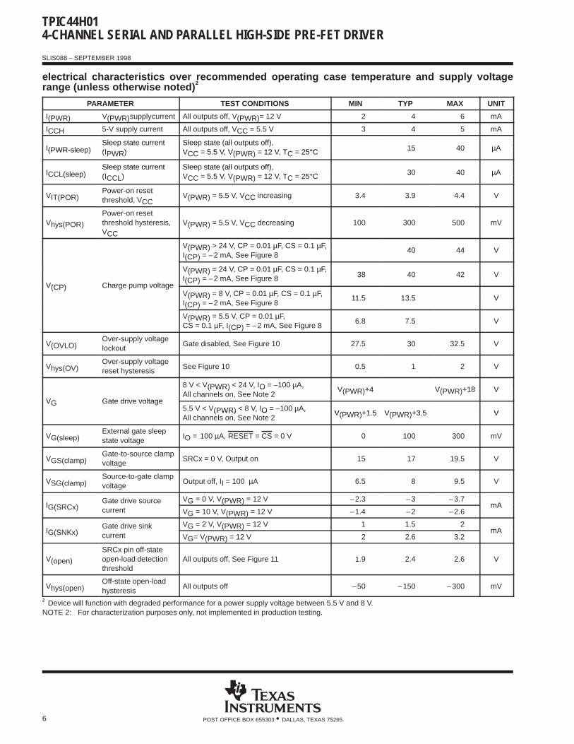
electrical characteristics over recommended operating case temperature and supply voltagerange (unless otherwise noted) †
PARAMETER TEST CONDITIONS MIN TYP MAX UNIT
I(PWR) V(PWR) supply current All outputs off, V(PWR)= 12 V 2 4 6 mA
ICCH 5-V supply current All outputs off, VCC = 5.5 V 3 4 5 mA
Sleep state current Sleep state (all outputs off)I(PWR-sleep)
Slee state current(IPWR)
Slee state (all out uts off),VCC 5 5 V V(PWR) 12 V TC 25°C 15 40 µAI(PWR-slee ) (IPWR) VCC = 5.5 V, V(PWR) = 12 V, TC = 25°C 15 40 µA
Sleep state current Sleep state (all outputs off)ICCL(sleep)
Slee state current(ICCL)
Slee state (all out uts off),VCC 5 5 V V(PWR) 12 V TC 25°C 30 40 µAICCL(slee ) (ICCL) VCC = 5.5 V, V(PWR) = 12 V, TC = 25°C 30 40 µA
VIT(POR)Power-on resetthreshold, VCC
V(PWR) = 5.5 V, VCC increasing 3.4 3.9 4.4 V
Vhys(POR)
Power-on resetthreshold hysteresis,VCC
V(PWR) = 5.5 V, VCC decreasing 100 300 500 mV
V(PWR) > 24 V, CP = 0.01 µF, CS = 0.1 µF,40 44 V(PWR) , µ , µ ,
I(CP) = –2 mA, See Figure 840 44 V
V(PWR) = 24 V CP = 0 01 µF CS = 0 1 µFV(PWR) = 24 V, CP = 0.01 µF, CS = 0.1 µF,I(CP) 2 mA See Figure 8 38 40 42 V
V(CP) Charge pump voltageI(CP) = –2 mA, See Figure 8 38 40 42 V
V(CP) Charge um voltageV(PWR) = 8 V, CP = 0.01 µF, CS = 0.1 µF,
11 5 13 5 V(PWR) , µ , µ ,I(CP) = –2 mA, See Figure 8
11.5 13.5 V
V(PWR) = 5.5 V, CP = 0.01 µF,CS = 0.1 µF, I(CP) = –2 mA, See Figure 8
6.8 7.5 V
V(OVLO)Over-supply voltagelockout
Gate disabled, See Figure 10 27.5 30 32.5 V
Vhys(OV)Over-supply voltagereset hysteresis
See Figure 10 0.5 1 2 V
8 V < V(PWR) < 24 V, IO = –100 µA,V(PWR)+4 V(PWR)+18 V
VG Gate drive voltage
(PWR) , O µ ,All channels on, See Note 2
V(PWR)+4 V(PWR)+18 V
VG Gate drive voltage5.5 V < V(PWR) < 8 V, IO = –100 µA,
V(PWR)+1 5 V(PWR)+3 5 V(PWR) , O µ ,All channels on, See Note 2
V(PWR)+1.5 V(PWR)+3.5 V
VG(sleep)External gate sleepstate voltage
IO = 100 µA, RESET = CS = 0 V 0 100 300 mV
VGS(clamp)Gate-to-source clampvoltage
SRCx = 0 V, Output on 15 17 19.5 V
VSG(clamp)Source-to-gate clampvoltage
Output off, II = 100 µA 6.5 8 9.5 V
IG(SRC )Gate drive source VG = 0 V, V(PWR) = 12 V –2.3 –3 –3.7
mAIG(SRCx) current VG = 10 V, V(PWR) = 12 V –1.4 –2 –2.6mA
IG(SNK )Gate drive sink VG = 2 V, V(PWR) = 12 V 1 1.5 2
mAIG(SNKx) current VG= V(PWR) = 12 V 2 2.6 3.2mA
V(open)
SRCx pin off-stateopen-load detectionthreshold
All outputs off, See Figure 11 1.9 2.4 2.6 V
Vhys(open)Off-state open-loadhysteresis
All outputs off –50 –150 –300 mV
† Device will function with degraded performance for a power supply voltage between 5.5 V and 8 V.NOTE 2: For characterization purposes only, not implemented in production testing.
TPIC44H014-CHANNEL SERIAL AND PARALLEL HIGH-SIDE PRE-FET DRIVER
SLIS088 – SEPTEMBER 1998
7POST OFFICE BOX 655303 • DALLAS, TEXAS 75265
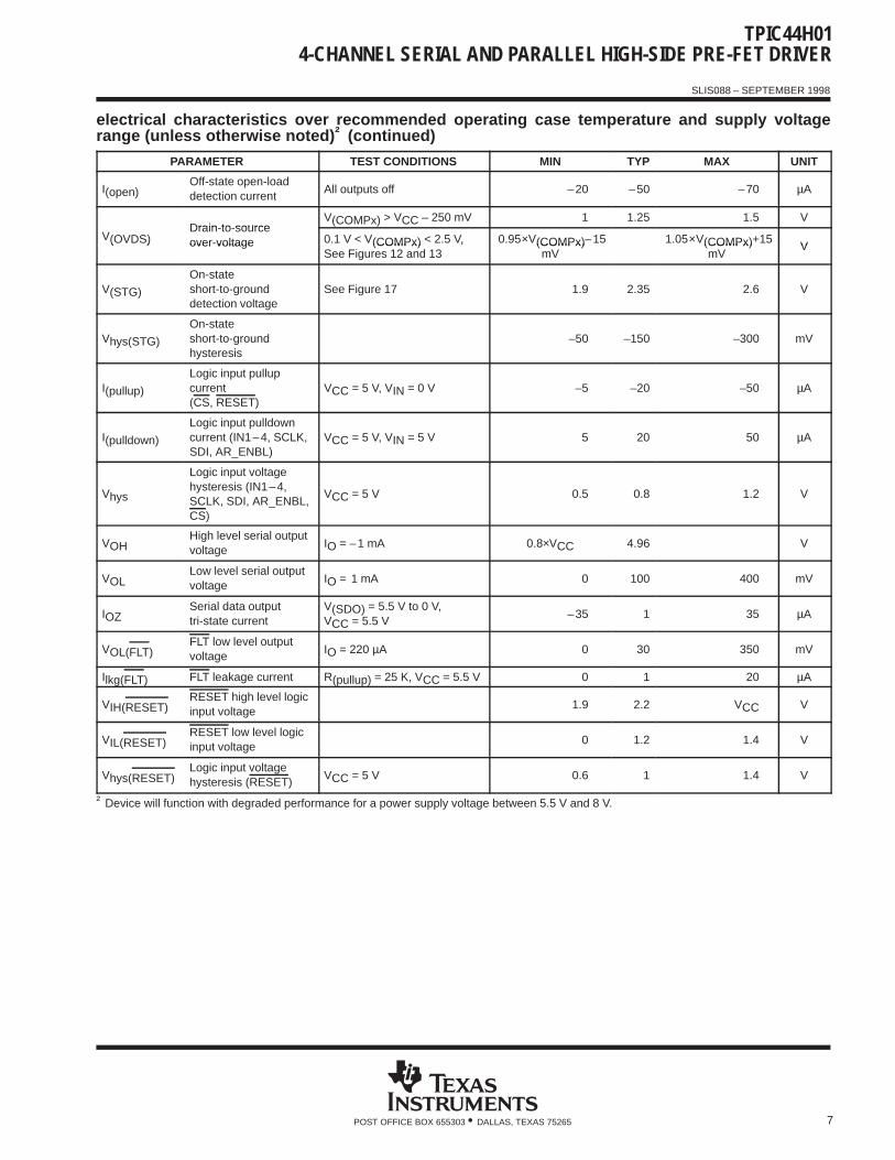
electrical characteristics over recommended operating case temperature and supply voltagerange (unless otherwise noted) † (continued)
PARAMETER TEST CONDITIONS MIN TYP MAX UNIT
I(open)Off-state open-loaddetection current
All outputs off –20 –50 –70 µA
Drain to sourceV(COMPx) > VCC – 250 mV 1 1.25 1.5 V
V(OVDS)Drain-to-sourceover-voltage 0.1 V < V(COMPx) < 2.5 V, 0.95 × V(COMPx)–15 1.05 × V(COMPx)+15
V( ) over voltage (COMPx) ,
See Figures 12 and 13(COMPx)mV
(COMPx)mV
V
V(STG)
On-stateshort-to-grounddetection voltage
See Figure 17 1.9 2.35 2.6 V
Vhys(STG)
On-stateshort-to-groundhysteresis
–50 –150 –300 mV
I(pullup)
Logic input pullupcurrent(CS, RESET)
VCC = 5 V, VIN = 0 V –5 –20 –50 µA
I(pulldown)
Logic input pulldowncurrent (IN1–4, SCLK,SDI, AR_ENBL)
VCC = 5 V, VIN = 5 V 5 20 50 µA
Vhys
Logic input voltagehysteresis (IN1–4,SCLK, SDI, AR_ENBL,CS)
VCC = 5 V 0.5 0.8 1.2 V
VOHHigh level serial outputvoltage
IO = –1 mA 0.8×VCC 4.96 V
VOLLow level serial outputvoltage
IO = 1 mA 0 100 400 mV
IOZSerial data outputtri-state current
V(SDO) = 5.5 V to 0 V,VCC = 5.5 V
–35 1 35 µA
VOL(FLT)FLT low level outputvoltage
IO = 220 µA 0 30 350 mV
Ilkg(FLT) FLT leakage current R(pullup) = 25 K, VCC = 5.5 V 0 1 20 µA
VIH(RESET)RESET high level logicinput voltage
1.9 2.2 VCC V
VIL(RESET)RESET low level logicinput voltage
0 1.2 1.4 V
Vhys(RESET)Logic input voltagehysteresis (RESET)
VCC = 5 V 0.6 1 1.4 V
† Device will function with degraded performance for a power supply voltage between 5.5 V and 8 V.
TPIC44H014-CHANNEL SERIAL AND PARALLEL HIGH-SIDE PRE-FET DRIVER
SLIS088 – SEPTEMBER 1998
8 POST OFFICE BOX 655303 • DALLAS, TEXAS 75265
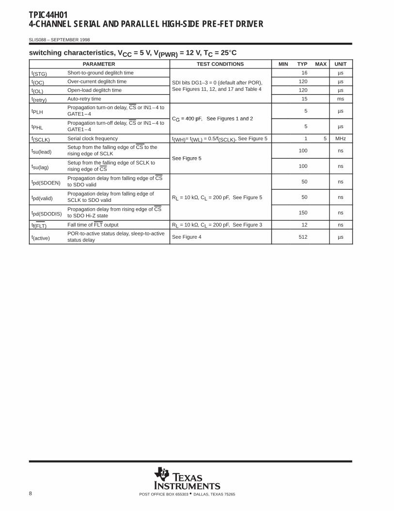
switching characteristics, V CC = 5 V, V(PWR) = 12 V, TC = 25°CPARAMETER TEST CONDITIONS MIN TYP MAX UNIT
t(STG) Short-to-ground deglitch time 16 µs
t(OC) Over-current deglitch time SDI bits DG1–3 = 0 (default after POR), 120 µs
t(OL) Open-load deglitch time
( ),See Figures 11, 12, and 17 and Table 4 120 µs
t(retry) Auto-retry time 15 ms
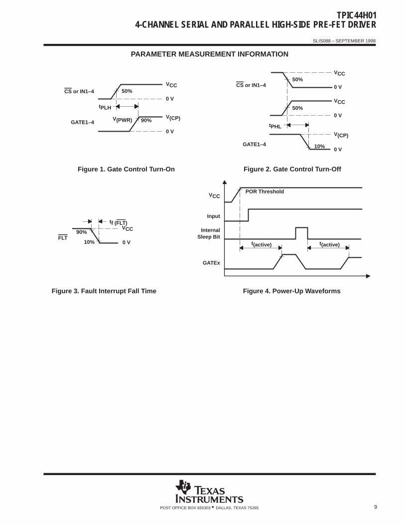
tPLHPropagation turn-on delay, CS or IN1–4 toGATE1–4
CG = 400 pF See Figures 1 and 2
5 µs
tPHLPropagation turn-off delay, CS or IN1–4 toGATE1–4
CG = 400 pF, See Figures 1 and 2
5 µs
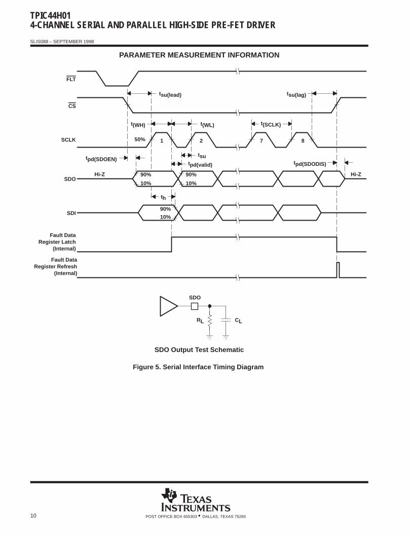
f(SCLK) Serial clock frequency t(WH)= t(WL) = 0.5/f(SCLK), See Figure 5 1 5 MHz
tsu(lead)Setup from the falling edge of CS to therising edge of SCLK
See Figure 5
100 ns
tsu(lag)Setup from the falling edge of SCLK torising edge of CS
See Figure 5
100 ns
tpd(SDOEN)Propagation delay from falling edge of CSto SDO valid
50 ns
tpd(valid)Propagation delay from falling edge ofSCLK to SDO valid RL = 10 kΩ, CL = 200 pF, See Figure 5 50 ns
tpd(SDODIS)Propagation delay from rising edge of CSto SDO Hi-Z state
150 ns
tf(FLT) Fall time of FLT output RL = 10 kΩ, CL = 200 pF, See Figure 3 12 ns
t(active)POR-to-active status delay, sleep-to-activestatus delay
See Figure 4 512 µs
TPIC44H014-CHANNEL SERIAL AND PARALLEL HIGH-SIDE PRE-FET DRIVER
SLIS088 – SEPTEMBER 1998
9POST OFFICE BOX 655303 • DALLAS, TEXAS 75265
PARAMETER MEASUREMENT INFORMATION
Figure 1. Gate Control Turn-On
tPLH
VCC
V(CP)
0 V
0 V
50%
V(PWR)
CS or IN1–4
GATE1–4 90%
Figure 2. Gate Control Turn-Off
50%
50%
VCC
0 V
tPHL
10%
V(CP)
0 V
CS or IN1–4
GATE1–4
VCC
0 V
Figure 3. Fault Interrupt Fall Time
VCC90%
10%
tf (FLT)
0 VFLT
Figure 4. Power-Up Waveforms
t(active) t(active)
POR ThresholdVCC
Input
InternalSleep Bit
GATEx
TPIC44H014-CHANNEL SERIAL AND PARALLEL HIGH-SIDE PRE-FET DRIVER
SLIS088 – SEPTEMBER 1998
10 POST OFFICE BOX 655303 • DALLAS, TEXAS 75265
PARAMETER MEASUREMENT INFORMATION
Figure 5. Serial Interface Timing Diagram
90%
10%
90%
10%
90%10%
tsu(lead)
t(WH) t(WL) t(SCLK)
tsu(lag)
tsu
50%
tpd(valid)tpd(SDOEN)
th
FLT
CS
SCLK
SDOHi-Z Hi-Z
SDI
Fault DataRegister Latch
(Internal)
Fault DataRegister Refresh
(Internal)
SDO
RL CL
1 2 7 8
tpd(SDODIS)
SDO Output Test Schematic
TPIC44H014-CHANNEL SERIAL AND PARALLEL HIGH-SIDE PRE-FET DRIVER
SLIS088 – SEPTEMBER 1998
11POST OFFICE BOX 655303 • DALLAS, TEXAS 75265
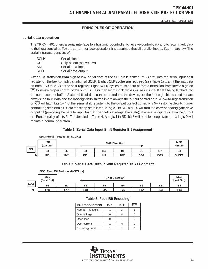
PRINCIPLES OF OPERATION
serial data operation
The TPIC44H01 offers a serial interface to a host microcontroller to receive control data and to return fault datato the host controller. For the serial interface operation, it is assumed that all parallel inputs, IN1–4, are low. Theserial interface consists of:
SCLK Serial clockCS Chip select (active low)SDI Serial data inputSDO Serial data output
After a CS transition from high to low, serial data at the SDI pin is shifted, MSB first, into the serial input shiftregister on the low-to-high transition of SCLK. Eight SCLK cycles are required (see Table 1) to shift the first databit from LSB to MSB of the shift register. Eight SCLK cycles must occur before a transition from low to high onCS to insure proper control of the outputs. Less than eight clock cycles will result in fault data being latched intothe output control buffer. Sixteen bits of data can be shifted into the device, but the first eight bits shifted out arealways the fault data and the last eight bits shifted in are always the output control data. A low-to-high transitionon CS will latch bits 1–4 of the serial shift register into the output control buffer, bits 5–7 into the deglitch timercontrol register, and bit 8 into the sleep state latch. A logic 0 in SDI bit1–4 will turn the corresponding gate driveoutput off (providing the parallel input for that channel is at a logic low state); likewise, a logic 1 will turn the outputon. Functionality of bits 5–7 is detailed in Table 4. A logic 1 in SDI bit 8 will enable sleep state and a logic 0 willmaintain normal operation.
Table 1. Serial Data Input Shift Register Bit Assignment
LSB(Last In)
MSB(First In)
SDIB1 B2 B3 B4 B5 B6 B7 B8
IN1 IN2 IN3 IN4 DG1 DG2 DG3 SLEEP
Shift Direction
SDI, Normal Protocol (8–SCLKs)
Table 2. Serial Data Output Shift Register Bit Assignment
MSB(First Out)
LSB(Last Out)
SDOB8 B7 B6 B5 B4 B3 B2 B1
F4B F4A F3B F3A F2B F2A F1B F1A
Shift Direction
SDO, Fault Bit Protocol (8–SCLKs)
Table 3. Fault Bit Encoding
FAULT CONDITION FxB FxA FLT
Normal – no faults X X 1
Over-voltage 0 0 0
Open-load 0 1 0
Over-current 1 0 0
Short-to-ground 1 1 0
TPIC44H014-CHANNEL SERIAL AND PARALLEL HIGH-SIDE PRE-FET DRIVER
SLIS088 – SEPTEMBER 1998
12 POST OFFICE BOX 655303 • DALLAS, TEXAS 75265
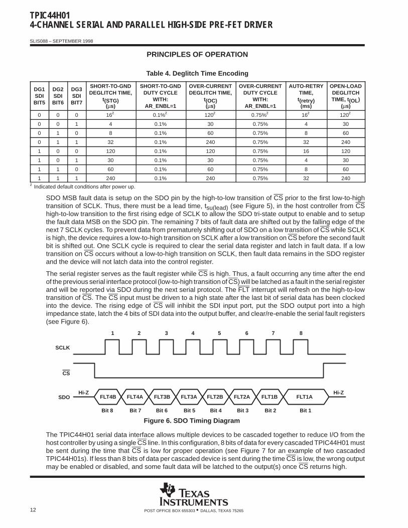
PRINCIPLES OF OPERATION
Table 4. Deglitch Time Encoding
DG1SDIBIT5
DG2SDIBIT6
DG3SDIBIT7
SHORT-TO-GNDDEGLITCH TIME,
t(STG)(µs)
SHORT-TO-GNDDUTY CYCLE
WITH:AR_ENBL=1
OVER-CURRENTDEGLITCH TIME,
t(OC)(µs)
OVER-CURRENTDUTY CYCLE
WITH:AR_ENBL=1
AUTO-RETRYTIME,
t(retry)(ms)
OPEN-LOADDEGLITCHTIME, t(OL)
(µs)
0 0 0 16† 0.1%† 120† 0.75%† 16† 120†
0 0 1 4 0.1% 30 0.75% 4 30
0 1 0 8 0.1% 60 0.75% 8 60
0 1 1 32 0.1% 240 0.75% 32 240
1 0 0 120 0.1% 120 0.75% 16 120
1 0 1 30 0.1% 30 0.75% 4 30
1 1 0 60 0.1% 60 0.75% 8 60
1 1 1 240 0.1% 240 0.75% 32 240† Indicated default conditions after power up.
SDO MSB fault data is setup on the SDO pin by the high-to-low transition of CS prior to the first low-to-hightransition of SCLK. Thus, there must be a lead time, tsu(lead) (see Figure 5), in the host controller from CShigh-to-low transition to the first rising edge of SCLK to allow the SDO tri-state output to enable and to setupthe fault data MSB on the SDO pin. The remaining 7 bits of fault data are shifted out by the falling edge of thenext 7 SCLK cycles. To prevent data from prematurely shifting out of SDO on a low transition of CS while SCLKis high, the device requires a low-to-high transition on SCLK after a low transition on CS before the second faultbit is shifted out. One SCLK cycle is required to clear the serial data register and latch in fault data. If a lowtransition on CS occurs without a low-to-high transition on SCLK, then fault data remains in the SDO registerand the device will not latch data into the control register.
The serial register serves as the fault register while CS is high. Thus, a fault occurring any time after the endof the previous serial interface protocol (low-to-high transition of CS) will be latched as a fault in the serial registerand will be reported via SDO during the next serial protocol. The FLT interrupt will refresh on the high-to-lowtransition of CS. The CS input must be driven to a high state after the last bit of serial data has been clockedinto the device. The rising edge of CS will inhibit the SDI input port, put the SDO output port into a highimpedance state, latch the 4 bits of SDI data into the output buffer, and clear/re-enable the serial fault registers(see Figure 6).
FLT4B FLT4A FLT3B FLT3A FLT2B FLT2A FLT1B FLT1AHi-Z Hi-Z
Bit 8 Bit 7 Bit 6 Bit 5 Bit 4 Bit 3 Bit 2 Bit 1
SCLK
CS
SDO
1 2 3 4 5 6 7 8
Figure 6. SDO Timing Diagram
The TPIC44H01 serial data interface allows multiple devices to be cascaded together to reduce I/O from thehost controller by using a single CS line. In this configuration, 8 bits of data for every cascaded TPIC44H01 mustbe sent during the time that CS is low for proper operation (see Figure 7 for an example of two cascadedTPIC44H01s). If less than 8 bits of data per cascaded device is sent during the time CS is low, the wrong outputmay be enabled or disabled, and some fault data will be latched to the output(s) once CS returns high.
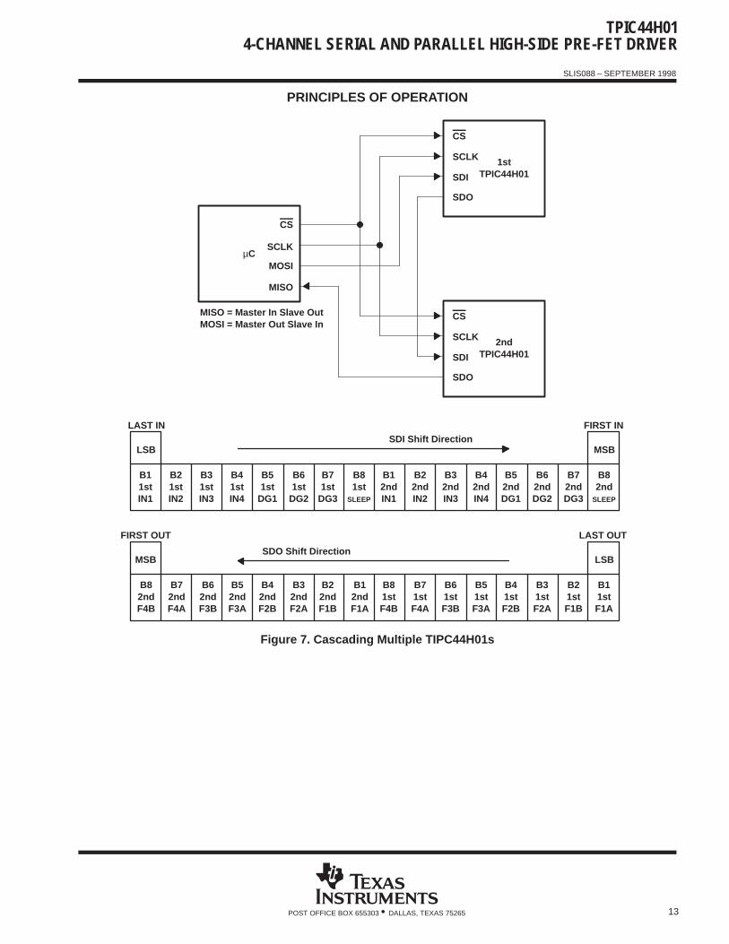
TPIC44H014-CHANNEL SERIAL AND PARALLEL HIGH-SIDE PRE-FET DRIVER
SLIS088 – SEPTEMBER 1998
13POST OFFICE BOX 655303 • DALLAS, TEXAS 75265
PRINCIPLES OF OPERATION
CS
SCLK
SDI
SDO
1stTPIC44H01
CS
SCLK
MOSI
MISO
µC
CS
SCLK
SDI
SDO
2ndTPIC44H01
MISO = Master In Slave OutMOSI = Master Out Slave In
B11stIN1
B21stIN2
B31stIN3
B41stIN4
B51st
DG1
B61st
DG2
B71st
DG3
B81st
SLEEP
B12ndIN1
B22ndIN2
B32ndIN3
B42ndIN4
B52ndDG1
B62ndDG2
B72ndDG3
B82nd
SLEEP
LSB MSB
LAST IN FIRST INSDI Shift Direction
SDO Shift Direction
B82ndF4B
B72ndF4A
B62ndF3B
B52ndF3A
B42ndF2B
B32ndF2A
B22ndF1B
B81stF4B
B71stF4A
B61stF3B
B51stF3A
B41stF2B
B31stF2A
B21stF1B
MSB LSB
FIRST OUT LAST OUT
B12ndF1A
B11stF1A
Figure 7. Cascading Multiple TIPC44H01s
TPIC44H014-CHANNEL SERIAL AND PARALLEL HIGH-SIDE PRE-FET DRIVER
SLIS088 – SEPTEMBER 1998
14 POST OFFICE BOX 655303 • DALLAS, TEXAS 75265
PRINCIPLES OF OPERATION
parallel input data operation
In addition to the serial interface, the TPIC44H01 also provides a parallel interface to control gate drive outputs.Parallel input is OR’ed with the serial interface control bit. Thus, the parallel inputs provide direct, real-timecontrol of the output drivers. SCLK and CS are not required to transfer parallel input data to the output buffer.Fault detection/protection is provided during parallel operation (see performance under fault conditionssection).
With AR_ENBL pin low, detection of an over-current or short-to-ground fault condition will disabled the gate driveuntil the auto-retry timer clears and re-enables the output.
CAUTION:If a parallel input is cycled low then high during auto-retry time, the timer is reset and the gate drivere-enable. The device will not prevent the user from switching at a higher duty cycle than theauto-retry function provides.
Serial fault data can be read over the serial data bus as described in the serial data operation section. If the FLTpin is latched low due to a fault detection, it cannot be cleared by cycling the parallel input. It can only be clearedby a low level on CS.
In applications where the serial interface and FLT interrupt are unused, CS should be tied high to disable theserial interface.
In applications where the serial interface or FLT interrupt are used only to retrieve fault data, care should betaken to program the SDI input low to prevent accidental activation of a gate drive output using a serial inputcontrol bit.
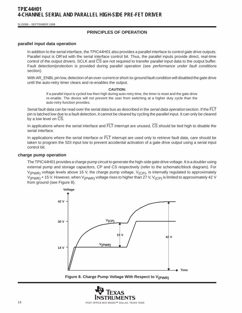
charge pump operation
The TPIC44H01 provides a charge pump circuit to generate the high-side gate drive voltage. It is a doubler usingexternal pump and storage capacitors, CP and CS respectively (refer to the schematic/block diagram). ForV(PWR) voltage levels above 16 V, the charge pump voltage, V(CP), is internally regulated to approximatelyV(PWR) + 15 V. However, when V(PWR) voltage rises to higher than 27 V, V(CP) is limited to approximately 42 Vfrom ground (see Figure 8).
15 V42 V
V(CP)
V(PWR)
Time
Voltage
42 V
30 V
14 V
Figure 8. Charge Pump Voltage With Respect to V (PWR)
TPIC44H014-CHANNEL SERIAL AND PARALLEL HIGH-SIDE PRE-FET DRIVER
SLIS088 – SEPTEMBER 1998
15POST OFFICE BOX 655303 • DALLAS, TEXAS 75265
PRINCIPLES OF OPERATION
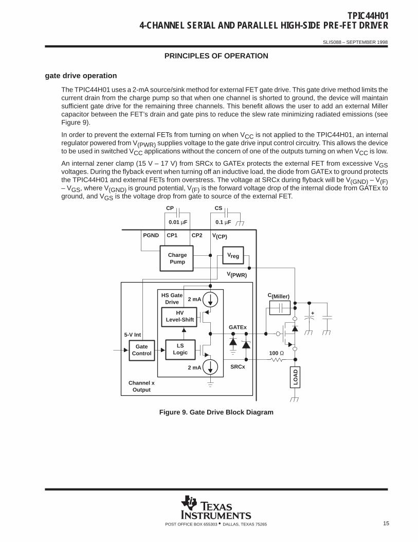
gate drive operation
The TPIC44H01 uses a 2-mA source/sink method for external FET gate drive. This gate drive method limits thecurrent drain from the charge pump so that when one channel is shorted to ground, the device will maintainsufficient gate drive for the remaining three channels. This benefit allows the user to add an external Millercapacitor between the FET’s drain and gate pins to reduce the slew rate minimizing radiated emissions (seeFigure 9).
In order to prevent the external FETs from turning on when VCC is not applied to the TPIC44H01, an internalregulator powered from V(PWR) supplies voltage to the gate drive input control circuitry. This allows the deviceto be used in switched VCC applications without the concern of one of the outputs turning on when VCC is low.
An internal zener clamp (15 V – 17 V) from SRCx to GATEx protects the external FET from excessive VGSvoltages. During the flyback event when turning off an inductive load, the diode from GATEx to ground protectsthe TPIC44H01 and external FETs from overstress. The voltage at SRCx during flyback will be V(GND) – V(F)– VGS, where V(GND) is ground potential, V(F) is the forward voltage drop of the internal diode from GATEx toground, and VGS is the voltage drop from gate to source of the external FET.
ChargePump
Vreg
HVLevel-Shift
LSLogic
LOA
D
GateControl
+
C(Miller)
GATEx
100 Ω
SRCx
0.01 µF 0.1 µF
CP
PGND CP1 CP2 V(CP)
V(PWR)
2 mA
2 mA
HS GateDrive
5-V Int
Channel xOutput
CS
Figure 9. Gate Drive Block Diagram
TPIC44H014-CHANNEL SERIAL AND PARALLEL HIGH-SIDE PRE-FET DRIVER
SLIS088 – SEPTEMBER 1998
16 POST OFFICE BOX 655303 • DALLAS, TEXAS 75265
PRINCIPLES OF OPERATION
performance under fault conditions
The TPIC44H01 is designed for normal operation over a supply voltage range of 8 V to 24 V with over-voltagefault detection typically at 30 V. The device offers on board fault detection to handle a variety of faults which mayoccur within a system. The primary function of the circuitry is to prevent damage to the load and the externalpower FETs in the event that a fault occurs, but off-state, open-load detection and reporting is also provided fordiagnostics. Note that unused SRC1–4 inputs must be connected to their respective GATE1–4 pins to preventfalse reporting of open-load fault conditions. Unused outputs with a SRC-to-GATE short should not becommanded on. For on-state faults, the circuitry detects the fault, shuts off the output to the FET, and reportsthe fault to the microcontroller. The primary faults monitored are:
1. V(PWR) over-voltage lockout (OVLO)2. Open-load3. Over-current4. Short-to-ground
FLT, fault interrupt operation
The FLT pin provides a real-time fault interrupt to signal a host controller that a fault has been detected. Anyof the four fault conditions listed above causes the FLT pin to be latched low immediately upon fault detection.
NOTE:Once FLT is latched low from a fault occurrence, it can only be cleared by a high-to-low transitionon CS.
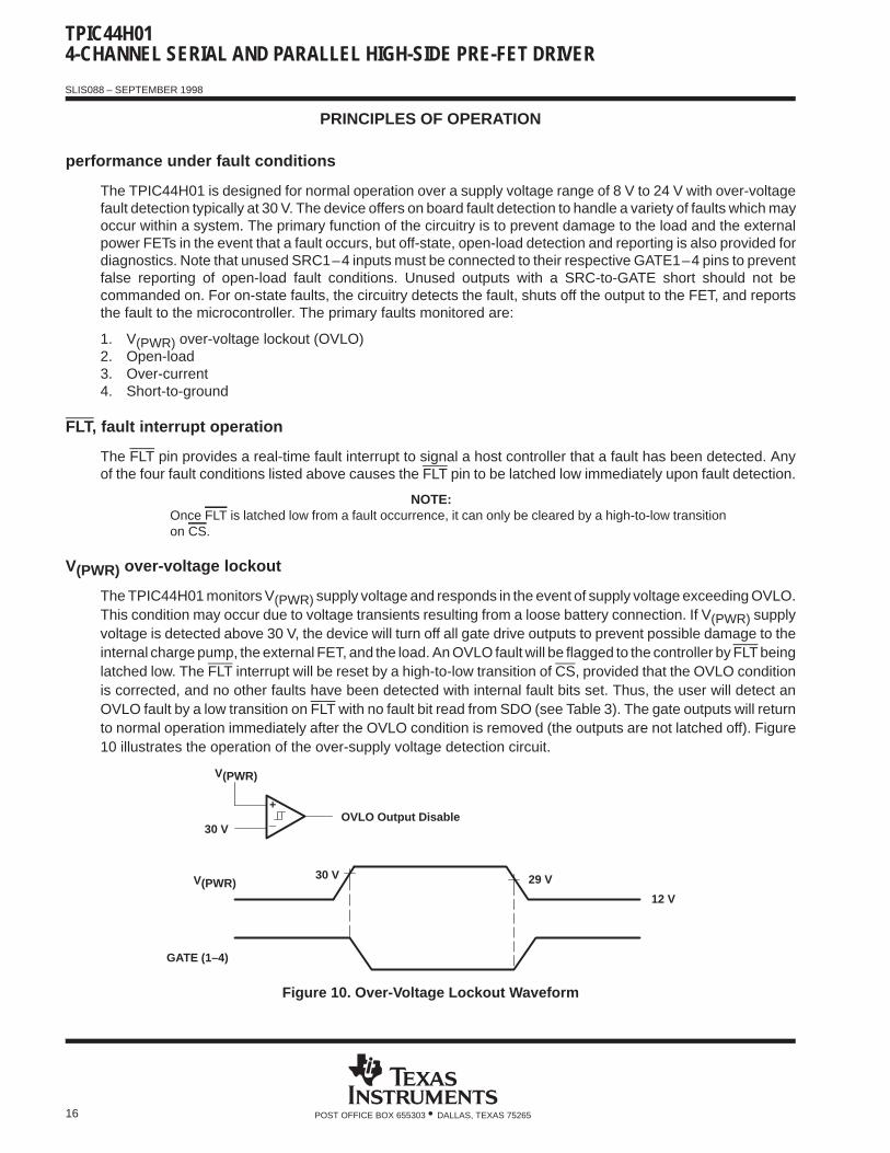
V(PWR) over-voltage lockout
The TPIC44H01 monitors V(PWR) supply voltage and responds in the event of supply voltage exceeding OVLO.This condition may occur due to voltage transients resulting from a loose battery connection. If V(PWR) supplyvoltage is detected above 30 V, the device will turn off all gate drive outputs to prevent possible damage to theinternal charge pump, the external FET, and the load. An OVLO fault will be flagged to the controller by FLT beinglatched low. The FLT interrupt will be reset by a high-to-low transition of CS, provided that the OVLO conditionis corrected, and no other faults have been detected with internal fault bits set. Thus, the user will detect anOVLO fault by a low transition on FLT with no fault bit read from SDO (see Table 3). The gate outputs will returnto normal operation immediately after the OVLO condition is removed (the outputs are not latched off). Figure10 illustrates the operation of the over-supply voltage detection circuit.
_+
30 V 29 V
12 V
V(PWR)
GATE (1–4)
OVLO Output Disable30 V
V(PWR)
Figure 10. Over-Voltage Lockout Waveform
TPIC44H014-CHANNEL SERIAL AND PARALLEL HIGH-SIDE PRE-FET DRIVER
SLIS088 – SEPTEMBER 1998
17POST OFFICE BOX 655303 • DALLAS, TEXAS 75265
PRINCIPLES OF OPERATION
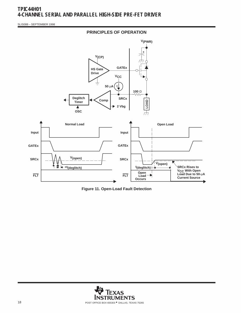
open load
An off-state, open-load condition is implemented in the TPIC44H01 by monitoring the SRCx terminal voltagewhen the FET is turned off by both the parallel input and the SDI bit being a logic 0. Figure 11 illustrates theoperation of the open-load detection circuit. When the GATEx output is low, thus turning off the FET (seeFigure 11), a 50-µA current is internally sourced from VCC to pull up the SRCx pin for open-load fault detection.
If the load is open, or if the impedance is substantially high, the 50-µA current source will cause the SRCx pinto rise above the ~2.4 V reference threshold of the open-load comparator. Unused SRC1–4 inputs must beconnected to their respective GATE1–4 pins to prevent false reporting of open-load fault conditions. An onboard deglitch timer starts when the open-load comparator detects a SRCx voltage greater than ~2.4 V,providing time for the SRCx voltage to stabilize after the power FET has been turned off. The SRCx voltage mustremain above the open-load detection threshold for the entire deglitch time, t(OL), (programmable, see Table 4)for the fault to be recognized as valid. If a valid fault is recognized, a real-time fault is flagged to the host controllerby latching the FLT pin low, and the appropriate fault bit is set. The host controller can read the serial SDO bitsto determine which channel reported the fault. Fault bits (1:8) distinguish faults for each of the output channels(see Table 2 and Table 3). This feature provides useful diagnostic information to the host controller totroubleshoot system failures and warn the operator that a problem exists.
If an open-load fault is detected by the TPIC44H01 while an output is off, the gate drive will be disabled the nexttime the output is commanded on either through the serial interface or the parallel inputs. In order to re-enablethe gate drive, the load must return to a normal condition and the user must toggle the input to the previouslyfaulted channel on then off then back on again.
NOTE:If an open-load fault is detected by the TPIC44H01 while an output is off and AR_ENBL = 0, thegate drive will be disabled the next time the output is commanded on either through the serialinterface or the parallel inputs. In order to re-enable the gate drive, the load must return to a normalcondition and the user must toggle the input to the previously faulted channel on then off then backon again.
NOTE:If an open-load fault is detected by the TPIC44H01 while an output is off and AR_ENBL = 1, theauto-retry timer will be initiated. This will cause the gate drive output to be delayed by t(retry) fromthe input signal. If more than one channel has detected an open-load fault, the delay from the inputsignal to the gate drive output signal will depend on which output detected the fault first. Thishappens because there is a single auto-retry timer used for all four channels. Normal operation willreturn once the fault condition is removed.
TPIC44H014-CHANNEL SERIAL AND PARALLEL HIGH-SIDE PRE-FET DRIVER
SLIS088 – SEPTEMBER 1998
18 POST OFFICE BOX 655303 • DALLAS, TEXAS 75265
PRINCIPLES OF OPERATION
OpenLoad
Occurs
LOA
D
+
100 Ω
HS GateDrive
Comp
50 µA
VCC
V(PWR)
2 Vbg
DeglitchTimer
OSC
GATEx
SRCx
V(CP)
I
<t(deglitch)
Normal Load
Input
GATEx
SRCx
FLT
V(open)t(deglitch)
Open Load
Input
GATEx
SRCx
FLT
SRCx Rises toVCC With OpenLoad Due to 50- µACurrent Source
V(open)
Figure 11. Open-Load Fault Detection
TPIC44H014-CHANNEL SERIAL AND PARALLEL HIGH-SIDE PRE-FET DRIVER
SLIS088 – SEPTEMBER 1998
19POST OFFICE BOX 655303 • DALLAS, TEXAS 75265
PRINCIPLES OF OPERATION
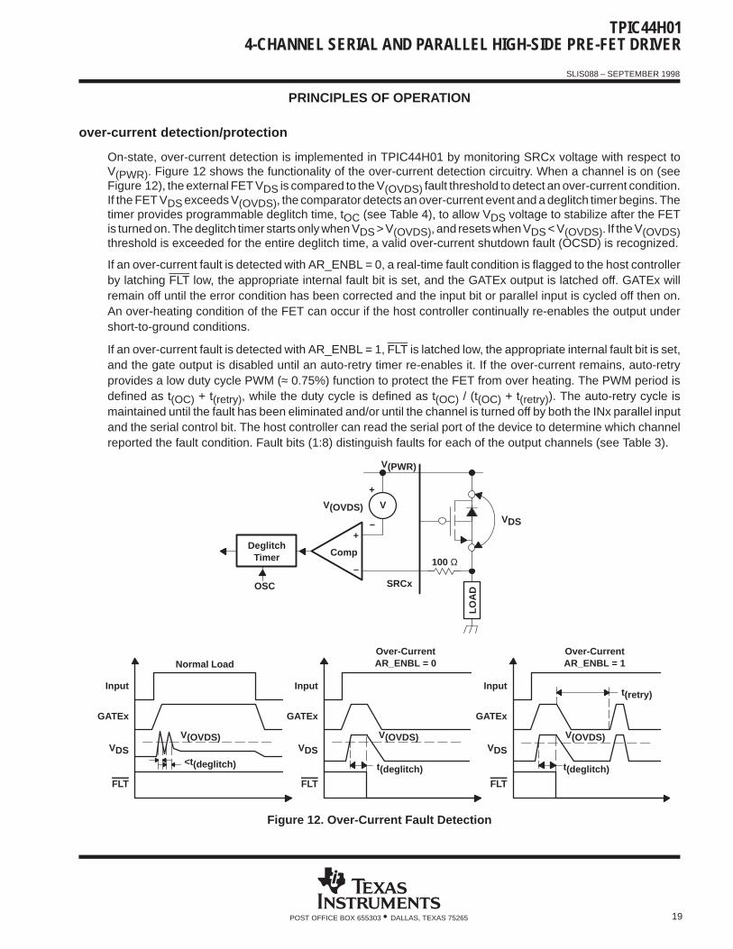
over-current detection/protection
On-state, over-current detection is implemented in TPIC44H01 by monitoring SRCx voltage with respect toV(PWR). Figure 12 shows the functionality of the over-current detection circuitry. When a channel is on (seeFigure 12), the external FET VDS is compared to the V(OVDS) fault threshold to detect an over-current condition.If the FET VDS exceeds V(OVDS), the comparator detects an over-current event and a deglitch timer begins. Thetimer provides programmable deglitch time, tOC (see Table 4), to allow VDS voltage to stabilize after the FETis turned on. The deglitch timer starts only when VDS > V(OVDS), and resets when VDS < V(OVDS). If the V(OVDS)threshold is exceeded for the entire deglitch time, a valid over-current shutdown fault (OCSD) is recognized.
If an over-current fault is detected with AR_ENBL = 0, a real-time fault condition is flagged to the host controllerby latching FLT low, the appropriate internal fault bit is set, and the GATEx output is latched off. GATEx willremain off until the error condition has been corrected and the input bit or parallel input is cycled off then on.An over-heating condition of the FET can occur if the host controller continually re-enables the output undershort-to-ground conditions.
If an over-current fault is detected with AR_ENBL = 1, FLT is latched low, the appropriate internal fault bit is set,and the gate output is disabled until an auto-retry timer re-enables it. If the over-current remains, auto-retryprovides a low duty cycle PWM (≈ 0.75%) function to protect the FET from over heating. The PWM period isdefined as t(OC) + t(retry), while the duty cycle is defined as t(OC) / (t(OC) + t(retry)). The auto-retry cycle ismaintained until the fault has been eliminated and/or until the channel is turned off by both the INx parallel inputand the serial control bit. The host controller can read the serial port of the device to determine which channelreported the fault condition. Fault bits (1:8) distinguish faults for each of the output channels (see Table 3).
LOA
D
100 ΩComp
V
DeglitchTimer
OSC
V(PWR)
SRCx
+
V(OVDS)
+
–
V(OVDS)
Input
GATEx
VDS
FLT
Normal Load
Input
GATEx
VDS
FLT
Over-CurrentAR_ENBL = 0
t(deglitch)
Input
GATEx
VDS
FLT
Over-CurrentAR_ENBL = 1
t(retry)
V(OVDS) V(OVDS)
t(deglitch)<t(deglitch)
– VDS
Figure 12. Over-Current Fault Detection

TPIC44H014-CHANNEL SERIAL AND PARALLEL HIGH-SIDE PRE-FET DRIVER
SLIS088 – SEPTEMBER 1998
20 POST OFFICE BOX 655303 • DALLAS, TEXAS 75265
PRINCIPLES OF OPERATION
external over-current threshold generation
The TPIC44H01 device provides several means for setting V(OVDS), the threshold voltage used to detectover-current. Figure 13 shows operation of the V(OVDS) generation circuitry. Any voltage appearing at theMUXOUT node (see Figure 13) will be forced across R1A, setting up a current equal to V(MUXOUT)/R1A. Thiscurrent is passed through R1B, a resistor matched to R1A, thereby generating an IR drop, V(OVDS), down fromV(PWR), which is identical to V(MUXOUT). The user can select either an internally generated ~1.25-V band-gapreference or can provide an external reference voltage using the V(COMPx) pin to control V(OV). The internalreference is selected by connecting the V(COMPx) pin to VCC. This forces a comparator with a threshold of VCC– V(F) to a state where it controls the analog AMUX block to connect MUXOUT to internal Vref.
A user adjustable V(OVDS) threshold can be set by supplying a voltage to the V(COMPx) pin in the range of 0.1to 2.5 V. With V(COMPx) voltage in this range, the comparator controlling AMUX is in the state where V(COMPx)voltage is connected to MUXOUT. Proper layout techniques should be used in the grounding network for theV(COMP) circuit on the TPIC44H01. Ground for the pre-driver and V(COMPx) network should be connected to aKelvin ground, if available. Otherwise, there should be a single point contact back to PGND of the FET array.Improper grounding techniques may result in inaccurate fault detection.
_
+Comp AMUX
_
+
Op-Amp
_
+Comp
VIO = ± 5 mV
VCC
R1B
R1A
1XBuffer
I
R1B/R1A Matching ± 5%
VIO = ± 10 mV
OVDSDetection
MUXOUTInternal
Vref(Vbg)VCC –V(F)
Switched bySerial InputBit or byParallel Input
Shared by Channels1 and 2 or 3 and 4
VCC V(PWR)
SRCx
V(PK_x)
V(COMPx)
VCC
VCC
R2
R3
R4
C1R5
V(OVDS)
NOTES: A. V(COMPx) should have at least 100 pF to ground to assure stability of the V(COMPx) amplifier.B. Equation for dynamic fault threshold voltage at V(COMP):
V(COMPx) (t) V(PK_x)e–tRC V(COMPx)(0)
Where V(COMPx)(t) is the voltage at V(COMPx) at time t, V(PK_x) is the voltage at V(PK_x) set by the R2 and R3 resistordivider, C is the value of C1, R is the parallel combination of R4 and R5, and V(COMPx)(0) is the voltage set up by the R4and R5 resistor divider.
(1)
Figure 13. Over-Current Fault Threshold Generation
TPIC44H014-CHANNEL SERIAL AND PARALLEL HIGH-SIDE PRE-FET DRIVER
SLIS088 – SEPTEMBER 1998
21POST OFFICE BOX 655303 • DALLAS, TEXAS 75265
PRINCIPLES OF OPERATION
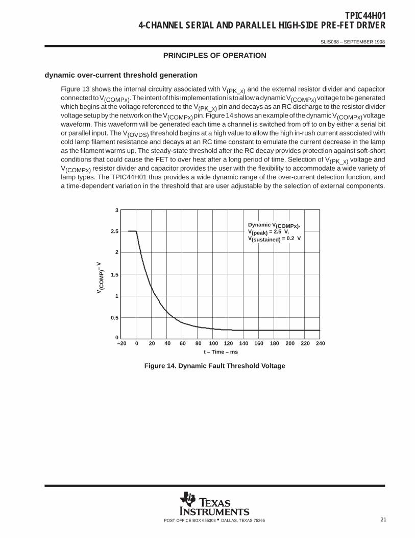
dynamic over-current threshold generation
Figure 13 shows the internal circuitry associated with V(PK_x) and the external resistor divider and capacitorconnected to V(COMPx). The intent of this implementation is to allow a dynamic V(COMPx) voltage to be generatedwhich begins at the voltage referenced to the V(PK_x) pin and decays as an RC discharge to the resistor dividervoltage setup by the network on the V(COMPx) pin. Figure 14 shows an example of the dynamic V(COMPx) voltagewaveform. This waveform will be generated each time a channel is switched from off to on by either a serial bitor parallel input. The V(OVDS) threshold begins at a high value to allow the high in-rush current associated withcold lamp filament resistance and decays at an RC time constant to emulate the current decrease in the lampas the filament warms up. The steady-state threshold after the RC decay provides protection against soft-shortconditions that could cause the FET to over heat after a long period of time. Selection of V(PK_x) voltage andV(COMPx) resistor divider and capacitor provides the user with the flexibility to accommodate a wide variety oflamp types. The TPIC44H01 thus provides a wide dynamic range of the over-current detection function, anda time-dependent variation in the threshold that are user adjustable by the selection of external components.
1.5
1
0.5
0–20 20 60 100
– V
2
2.5
t – Time – ms
3
140 180 220
V(C
OM
P)
0 40 80 120 160 200 240
Dynamic V (COMPx),V(peak) = 2.5 V,V(sustained) = 0.2 V
Figure 14. Dynamic Fault Threshold Voltage
TPIC44H014-CHANNEL SERIAL AND PARALLEL HIGH-SIDE PRE-FET DRIVER
SLIS088 – SEPTEMBER 1998
22 POST OFFICE BOX 655303 • DALLAS, TEXAS 75265
PRINCIPLES OF OPERATION
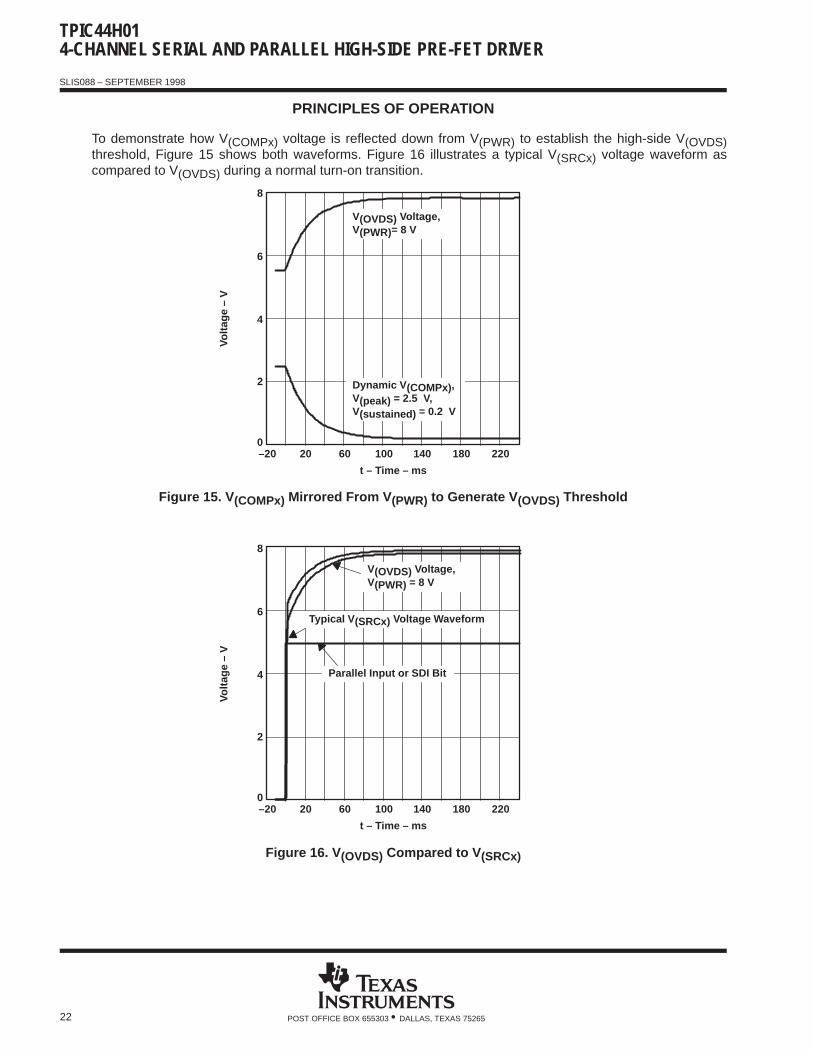
To demonstrate how V(COMPx) voltage is reflected down from V(PWR) to establish the high-side V(OVDS)threshold, Figure 15 shows both waveforms. Figure 16 illustrates a typical V(SRCx) voltage waveform ascompared to V(OVDS) during a normal turn-on transition.
4
2
0–20 20 60 100
6
t – Time – ms
8
140 180 220
V(OVDS) Voltage,V(PWR)= 8 V
Dynamic V (COMPx),V(peak) = 2.5 V,V(sustained) = 0.2 V
Volta
ge –
V
Figure 15. V (COMPx) Mirrored From V (PWR) to Generate V (OVDS) Threshold
0
4
6
8
2
–20 20 60 100
t – Time – ms
140 180 220
Volta
ge –
V
V(OVDS) Voltage,V(PWR) = 8 V
Typical V (SRCx) Voltage Waveform
Parallel Input or SDI Bit
Figure 16. V (OVDS) Compared to V (SRCx)
TPIC44H014-CHANNEL SERIAL AND PARALLEL HIGH-SIDE PRE-FET DRIVER
SLIS088 – SEPTEMBER 1998
23POST OFFICE BOX 655303 • DALLAS, TEXAS 75265
PRINCIPLES OF OPERATION
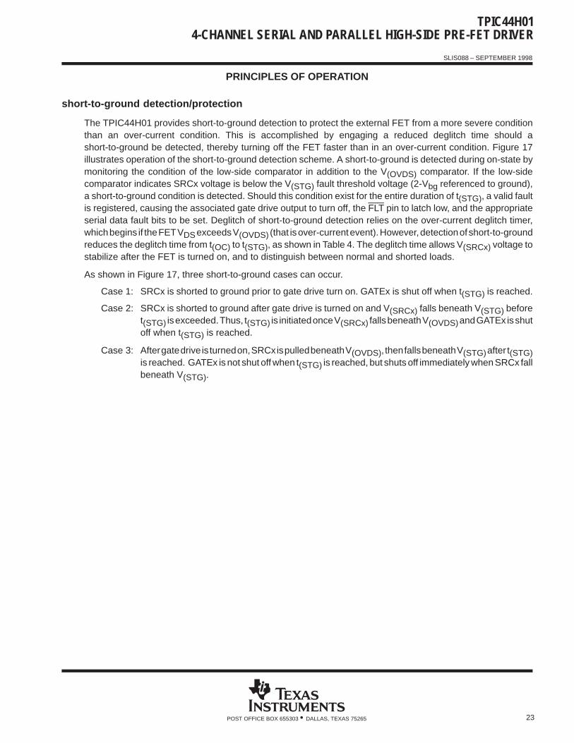
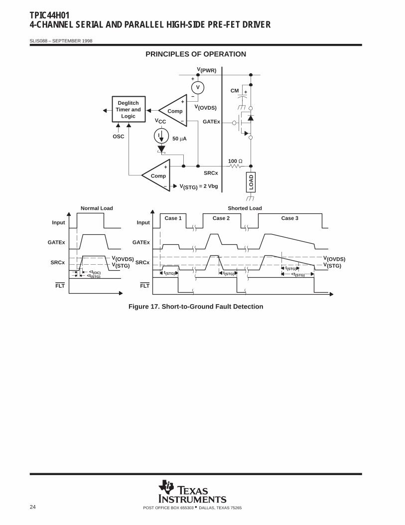
short-to-ground detection/protection
The TPIC44H01 provides short-to-ground detection to protect the external FET from a more severe conditionthan an over-current condition. This is accomplished by engaging a reduced deglitch time should ashort-to-ground be detected, thereby turning off the FET faster than in an over-current condition. Figure 17illustrates operation of the short-to-ground detection scheme. A short-to-ground is detected during on-state bymonitoring the condition of the low-side comparator in addition to the V(OVDS) comparator. If the low-sidecomparator indicates SRCx voltage is below the V(STG) fault threshold voltage (2-Vbg referenced to ground),a short-to-ground condition is detected. Should this condition exist for the entire duration of t(STG), a valid faultis registered, causing the associated gate drive output to turn off, the FLT pin to latch low, and the appropriateserial data fault bits to be set. Deglitch of short-to-ground detection relies on the over-current deglitch timer,which begins if the FET VDS exceeds V(OVDS) (that is over-current event). However, detection of short-to-groundreduces the deglitch time from t(OC) to t(STG), as shown in Table 4. The deglitch time allows V(SRCx) voltage tostabilize after the FET is turned on, and to distinguish between normal and shorted loads.
As shown in Figure 17, three short-to-ground cases can occur.
Case 1: SRCx is shorted to ground prior to gate drive turn on. GATEx is shut off when t(STG) is reached.
Case 2: SRCx is shorted to ground after gate drive is turned on and V(SRCx) falls beneath V(STG) beforet(STG) is exceeded. Thus, t(STG) is initiated once V(SRCx) falls beneath V(OVDS) and GATEx is shutoff when t(STG) is reached.
Case 3: After gate drive is turned on, SRCx is pulled beneath V(OVDS), then falls beneath V(STG) after t(STG)is reached. GATEx is not shut off when t(STG) is reached, but shuts off immediately when SRCx fallbeneath V(STG).
TPIC44H014-CHANNEL SERIAL AND PARALLEL HIGH-SIDE PRE-FET DRIVER
SLIS088 – SEPTEMBER 1998
24 POST OFFICE BOX 655303 • DALLAS, TEXAS 75265
PRINCIPLES OF OPERATION
t(STG)
t(STG)
LOA
D
+
100 Ω
Comp
50 µA
VCC
V(PWR)
V(STG) = 2 Vbg
DeglitchTimer and
LogicGATEx
SRCx
OSC I
Comp
V
V(OVDS)
+
–+
–
+
–
CM
<t(OC)
Normal Load
Input
GATEx
SRCx
FLT
V(OVDS) V(OVDS)V(STG)
<t(STG)
Shorted Load
Case 1 Case 2 Case 3Input
GATEx
SRCx
FLT
t(STG)<t(STG)
V(STG)
Figure 17. Short-to-Ground Fault Detection
TPIC44H014-CHANNEL SERIAL AND PARALLEL HIGH-SIDE PRE-FET DRIVER
SLIS088 – SEPTEMBER 1998
25POST OFFICE BOX 655303 • DALLAS, TEXAS 75265
PRINCIPLES OF OPERATION
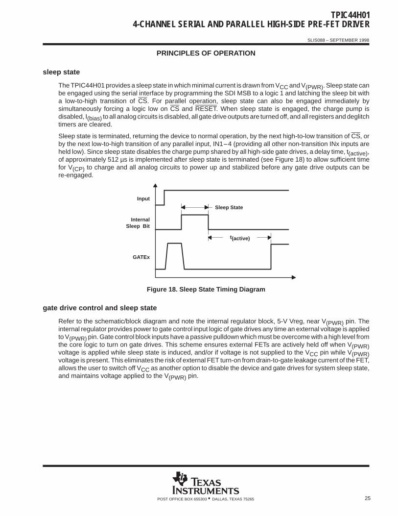
sleep state
The TPIC44H01 provides a sleep state in which minimal current is drawn from VCC and V(PWR). Sleep state canbe engaged using the serial interface by programming the SDI MSB to a logic 1 and latching the sleep bit witha low-to-high transition of CS. For parallel operation, sleep state can also be engaged immediately bysimultaneously forcing a logic low on CS and RESET. When sleep state is engaged, the charge pump isdisabled, I(bias) to all analog circuits is disabled, all gate drive outputs are turned off, and all registers and deglitchtimers are cleared.
Sleep state is terminated, returning the device to normal operation, by the next high-to-low transition of CS, orby the next low-to-high transition of any parallel input, IN1–4 (providing all other non-transition INx inputs areheld low). Since sleep state disables the charge pump shared by all high-side gate drives, a delay time, t(active),of approximately 512 µs is implemented after sleep state is terminated (see Figure 18) to allow sufficient timefor V(CP) to charge and all analog circuits to power up and stabilized before any gate drive outputs can bere-engaged.
Sleep State
t(active)
Input
InternalSleep Bit
GATEx
Figure 18. Sleep State Timing Diagram
gate drive control and sleep state
Refer to the schematic/block diagram and note the internal regulator block, 5-V Vreg, near V(PWR) pin. Theinternal regulator provides power to gate control input logic of gate drives any time an external voltage is appliedto V(PWR) pin. Gate control block inputs have a passive pulldown which must be overcome with a high level fromthe core logic to turn on gate drives. This scheme ensures external FETs are actively held off when V(PWR)voltage is applied while sleep state is induced, and/or if voltage is not supplied to the VCC pin while V(PWR)voltage is present. This eliminates the risk of external FET turn-on from drain-to-gate leakage current of the FET,allows the user to switch off VCC as another option to disable the device and gate drives for system sleep state,and maintains voltage applied to the V(PWR) pin.
TPIC44H014-CHANNEL SERIAL AND PARALLEL HIGH-SIDE PRE-FET DRIVER
SLIS088 – SEPTEMBER 1998
26 POST OFFICE BOX 655303 • DALLAS, TEXAS 75265
PRINCIPLES OF OPERATION
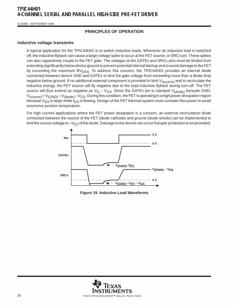
inductive voltage transients
A typical application for the TPIC44H01 is to switch inductive loads. Whenever an inductive load is switchedoff, the inductive flyback can cause a large voltage spike to occur at the FET source, or SRCx pin. These spikescan also capacitively couple to the FET gate. The voltages at the GATEx and SRCx pins must be limited fromextending significantly below device ground to prevent potential internal latchup and to avoid damage to the FETby exceeding the maximum BVDSS. To address this concern, the TPIC44H01 provides an internal diodeconnected between device GND and GATEx to limit the gate voltage from exceeding more than a diode dropnegative below ground. If no additional external component is provided to limit V(source) and to recirculate theinductive energy, the FET source will fly negative due to the load inductive flyback during turn-off. The FETsource will thus extend as negative as VG – VGS. Since the GATEx pin is clamped V(diode) beneath GND,V(source) = V(GND) – V(diode) – VGS. During this condition, the FET is operating in a high power dissipation regionbecause VDS is large while IDS is flowing. Design of the FET thermal system must consider this power to avoidexcessive junction temperature.
For high current applications where the FET power dissipation is a concern, an external recirculation diodeconnected between the source of the FET (diode cathode) and ground (diode anode) can be implemented tolimit the source voltage to –V(F) of the diode. Damage to the device can occur if proper protection is not provided.
V(GND)–V(F)
V(GND) –V(F) – VGS
INx
GATEx
SRCx
5 V
0 V
V(PWR) – VDS
0 V
Figure 19. Inductive Load Waveforms
PACKAGE OPTION ADDENDUM
www.ti.com 29-Dec-2015
Addendum-Page 1
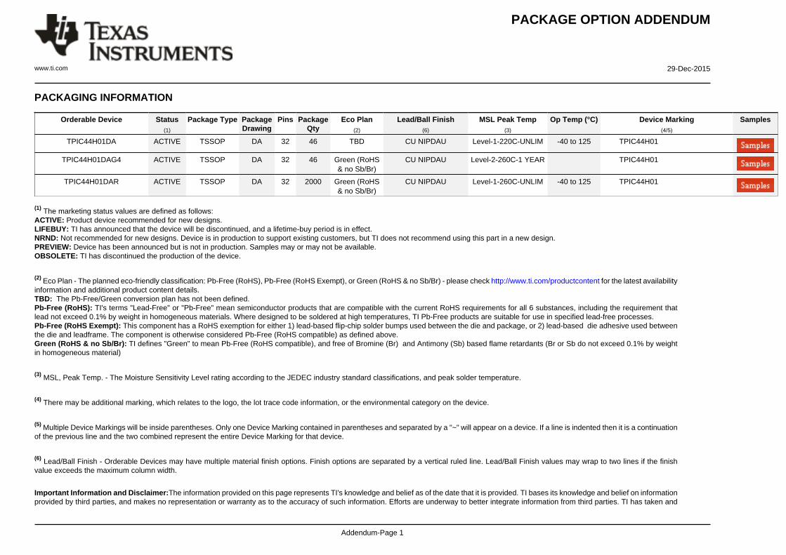
PACKAGING INFORMATION
Orderable Device Status(1)
Package Type PackageDrawing
Pins PackageQty
Eco Plan(2)
Lead/Ball Finish(6)
MSL Peak Temp(3)
Op Temp (°C) Device Marking(4/5)
Samples
TPIC44H01DA ACTIVE TSSOP DA 32 46 TBD CU NIPDAU Level-1-220C-UNLIM -40 to 125 TPIC44H01
TPIC44H01DAG4 ACTIVE TSSOP DA 32 46 Green (RoHS& no Sb/Br)
CU NIPDAU Level-2-260C-1 YEAR TPIC44H01
TPIC44H01DAR ACTIVE TSSOP DA 32 2000 Green (RoHS& no Sb/Br)
CU NIPDAU Level-1-260C-UNLIM -40 to 125 TPIC44H01
(1) The marketing status values are defined as follows:ACTIVE: Product device recommended for new designs.LIFEBUY: TI has announced that the device will be discontinued, and a lifetime-buy period is in effect.NRND: Not recommended for new designs. Device is in production to support existing customers, but TI does not recommend using this part in a new design.PREVIEW: Device has been announced but is not in production. Samples may or may not be available.OBSOLETE: TI has discontinued the production of the device.
(2) Eco Plan - The planned eco-friendly classification: Pb-Free (RoHS), Pb-Free (RoHS Exempt), or Green (RoHS & no Sb/Br) - please check http://www.ti.com/productcontent for the latest availabilityinformation and additional product content details.TBD: The Pb-Free/Green conversion plan has not been defined.Pb-Free (RoHS): TI's terms "Lead-Free" or "Pb-Free" mean semiconductor products that are compatible with the current RoHS requirements for all 6 substances, including the requirement thatlead not exceed 0.1% by weight in homogeneous materials. Where designed to be soldered at high temperatures, TI Pb-Free products are suitable for use in specified lead-free processes.Pb-Free (RoHS Exempt): This component has a RoHS exemption for either 1) lead-based flip-chip solder bumps used between the die and package, or 2) lead-based die adhesive used betweenthe die and leadframe. The component is otherwise considered Pb-Free (RoHS compatible) as defined above.Green (RoHS & no Sb/Br): TI defines "Green" to mean Pb-Free (RoHS compatible), and free of Bromine (Br) and Antimony (Sb) based flame retardants (Br or Sb do not exceed 0.1% by weightin homogeneous material)
(3) MSL, Peak Temp. - The Moisture Sensitivity Level rating according to the JEDEC industry standard classifications, and peak solder temperature.
(4) There may be additional marking, which relates to the logo, the lot trace code information, or the environmental category on the device.
(5) Multiple Device Markings will be inside parentheses. Only one Device Marking contained in parentheses and separated by a "~" will appear on a device. If a line is indented then it is a continuationof the previous line and the two combined represent the entire Device Marking for that device.
(6) Lead/Ball Finish - Orderable Devices may have multiple material finish options. Finish options are separated by a vertical ruled line. Lead/Ball Finish values may wrap to two lines if the finishvalue exceeds the maximum column width.
Important Information and Disclaimer:The information provided on this page represents TI's knowledge and belief as of the date that it is provided. TI bases its knowledge and belief on informationprovided by third parties, and makes no representation or warranty as to the accuracy of such information. Efforts are underway to better integrate information from third parties. TI has taken and
PACKAGE OPTION ADDENDUM
www.ti.com 29-Dec-2015
Addendum-Page 2
continues to take reasonable steps to provide representative and accurate information but may not have conducted destructive testing or chemical analysis on incoming materials and chemicals.TI and TI suppliers consider certain information to be proprietary, and thus CAS numbers and other limited information may not be available for release.
In no event shall TI's liability arising out of such information exceed the total purchase price of the TI part(s) at issue in this document sold by TI to Customer on an annual basis.
TAPE AND REEL INFORMATION
*All dimensions are nominal
Device PackageType
PackageDrawing
Pins SPQ ReelDiameter
(mm)
ReelWidth
W1 (mm)
A0(mm)
B0(mm)
K0(mm)
P1(mm)
W(mm)
Pin1Quadrant
TPIC44H01DAR TSSOP DA 32 2000 330.0 24.4 8.6 11.5 1.6 12.0 24.0 Q1
PACKAGE MATERIALS INFORMATION
www.ti.com 30-Dec-2015
Pack Materials-Page 1
*All dimensions are nominal
Device Package Type Package Drawing Pins SPQ Length (mm) Width (mm) Height (mm)
TPIC44H01DAR TSSOP DA 32 2000 367.0 367.0 45.0
PACKAGE MATERIALS INFORMATION
www.ti.com 30-Dec-2015
Pack Materials-Page 2
IMPORTANT NOTICE
Texas Instruments Incorporated and its subsidiaries (TI) reserve the right to make corrections, enhancements, improvements and otherchanges to its semiconductor products and services per JESD46, latest issue, and to discontinue any product or service per JESD48, latestissue. Buyers should obtain the latest relevant information before placing orders and should verify that such information is current andcomplete. All semiconductor products (also referred to herein as “components”) are sold subject to TI’s terms and conditions of salesupplied at the time of order acknowledgment.TI warrants performance of its components to the specifications applicable at the time of sale, in accordance with the warranty in TI’s termsand conditions of sale of semiconductor products. Testing and other quality control techniques are used to the extent TI deems necessaryto support this warranty. Except where mandated by applicable law, testing of all parameters of each component is not necessarilyperformed.TI assumes no liability for applications assistance or the design of Buyers’ products. Buyers are responsible for their products andapplications using TI components. To minimize the risks associated with Buyers’ products and applications, Buyers should provideadequate design and operating safeguards.TI does not warrant or represent that any license, either express or implied, is granted under any patent right, copyright, mask work right, orother intellectual property right relating to any combination, machine, or process in which TI components or services are used. Informationpublished by TI regarding third-party products or services does not constitute a license to use such products or services or a warranty orendorsement thereof. Use of such information may require a license from a third party under the patents or other intellectual property of thethird party, or a license from TI under the patents or other intellectual property of TI.Reproduction of significant portions of TI information in TI data books or data sheets is permissible only if reproduction is without alterationand is accompanied by all associated warranties, conditions, limitations, and notices. TI is not responsible or liable for such altereddocumentation. Information of third parties may be subject to additional restrictions.Resale of TI components or services with statements different from or beyond the parameters stated by TI for that component or servicevoids all express and any implied warranties for the associated TI component or service and is an unfair and deceptive business practice.TI is not responsible or liable for any such statements.Buyer acknowledges and agrees that it is solely responsible for compliance with all legal, regulatory and safety-related requirementsconcerning its products, and any use of TI components in its applications, notwithstanding any applications-related information or supportthat may be provided by TI. Buyer represents and agrees that it has all the necessary expertise to create and implement safeguards whichanticipate dangerous consequences of failures, monitor failures and their consequences, lessen the likelihood of failures that might causeharm and take appropriate remedial actions. Buyer will fully indemnify TI and its representatives against any damages arising out of the useof any TI components in safety-critical applications.In some cases, TI components may be promoted specifically to facilitate safety-related applications. With such components, TI’s goal is tohelp enable customers to design and create their own end-product solutions that meet applicable functional safety standards andrequirements. Nonetheless, such components are subject to these terms.No TI components are authorized for use in FDA Class III (or similar life-critical medical equipment) unless authorized officers of the partieshave executed a special agreement specifically governing such use.Only those TI components which TI has specifically designated as military grade or “enhanced plastic” are designed and intended for use inmilitary/aerospace applications or environments. Buyer acknowledges and agrees that any military or aerospace use of TI componentswhich have not been so designated is solely at the Buyer's risk, and that Buyer is solely responsible for compliance with all legal andregulatory requirements in connection with such use.TI has specifically designated certain components as meeting ISO/TS16949 requirements, mainly for automotive use. In any case of use ofnon-designated products, TI will not be responsible for any failure to meet ISO/TS16949.
Products ApplicationsAudio www.ti.com/audio Automotive and Transportation www.ti.com/automotiveAmplifiers amplifier.ti.com Communications and Telecom www.ti.com/communicationsData Converters dataconverter.ti.com Computers and Peripherals www.ti.com/computersDLP® Products www.dlp.com Consumer Electronics www.ti.com/consumer-appsDSP dsp.ti.com Energy and Lighting www.ti.com/energyClocks and Timers www.ti.com/clocks Industrial www.ti.com/industrialInterface interface.ti.com Medical www.ti.com/medicalLogic logic.ti.com Security www.ti.com/securityPower Mgmt power.ti.com Space, Avionics and Defense www.ti.com/space-avionics-defenseMicrocontrollers microcontroller.ti.com Video and Imaging www.ti.com/videoRFID www.ti-rfid.comOMAP Applications Processors www.ti.com/omap TI E2E Community e2e.ti.comWireless Connectivity www.ti.com/wirelessconnectivity
Mailing Address: Texas Instruments, Post Office Box 655303, Dallas, Texas 75265Copyright © 2015, Texas Instruments Incorporated