Embed Size (px)
Citation preview

1.8 V
3.3-V to 1.8-VTranslators
VREG
VOFFSET
DLP470NEDMD
TPS65145(Voltage
Regulator) VRESET
PG_OFFSET
VBIAS
EN_OFFSET
DLPC4422 ASIC
DAD control
3.3 V
SCP control
DMD RSTZ
Control Signals DLPA100Colorwheel Motor Control
ASIC Power
Copyright © 2017, Texas Instruments Incorporated
Product
Folder
Order
Now
Technical
Documents
Tools &
Software
Support &Community
An IMPORTANT NOTICE at the end of this data sheet addresses availability, warranty, changes, use in safety-critical applications,intellectual property matters and other important disclaimers. PRODUCTION DATA.
DLP470NEDLPS091 –AUGUST 2017
DLP470NE 0.47 1080P DMD
1
1 Features1• 0.47-Inch Diagonal Micromirror Array
– Full HD/1080P (1920 x 1080)– 5.4 Micron Micromirror Pitch– ±17° Micromirror Tilt (Relative to Flat Surface)– Bottom Illumination
• 2 × LVDS Input Data Bus• Dedicated DLPC4422 Display Controller,
DLPA100 Power Management IC and MotorDriver for reliable operation
2 Applications• Full HD (1080P) Display• Laser TV• Mobile Smart TV• Digital Signage• Gaming• Home Cinema
3 DescriptionThe TI DLP470NE digital micromirror device (DMD) isa digitally controlled micro-electromechanical system(MEMS) spatial light modulator (SLM) that enablesbright full HD display systems. DLP470NE DMD isonly 0.47-inches in size, yet delivers bright imagesand video up to 4000 lumens. The DLP470NE DMD,together with the DLPC4422 display controller andDLPA100 power and motor driver, comprise theDLP® 0.47” 1080P chipset. This solution is great fitfor many high brightness 1080P/HD display systems.
Device Information(1)
PART NUMBER PACKAGE BODY SIZE (NOM)DLP470NE FXH (257) 32 mm × 22 mm
(1) For all available packages, see the orderable addendum atthe end of the data sheet.
DLP470NE 0.47 1080P DMD
2
DLP470NEDLPS091 –AUGUST 2017 www.ti.com
Product Folder Links: DLP470NE
Submit Documentation Feedback Copyright © 2017, Texas Instruments Incorporated
Table of Contents1 Features .................................................................. 12 Applications ........................................................... 13 Description ............................................................. 14 Revision History..................................................... 25 Pin Configuration and Functions ......................... 36 Specifications....................................................... 10
6.1 Absolute Maximum Ratings .................................... 106.2 Storage Conditions.................................................. 106.3 ESD Ratings............................................................ 116.4 Recommended Operating Conditions..................... 116.5 Thermal Information ................................................ 136.6 Electrical Characteristics......................................... 146.7 Capacitance at Recommended Operating
Conditions ................................................................ 146.8 Timing Requirements .............................................. 156.9 System Mounting Interface Loads .......................... 176.10 Micromirror Array Physical Characteristics ........... 186.11 Micromirror Array Optical Characteristics ............. 206.12 Window Characteristics......................................... 216.13 Chipset Component Usage Specification ............. 21
7 Detailed Description ............................................ 227.1 Overview ................................................................. 227.2 Functional Block Diagram ....................................... 237.3 Feature Description................................................. 24
7.4 Device Functional Modes........................................ 247.5 Window Characteristics and Optics ........................ 247.6 Micromirror Array Temperature Calculation............ 267.7 Micromirror Landed-On/Landed-Off Duty Cycle ..... 27
8 Application and Implementation ........................ 308.1 Application Information............................................ 308.2 Typical Application ................................................. 30
9 Power Supply Recommendations ...................... 339.1 DMD Power Supply Power-Up Procedure.............. 339.2 DMD Power Supply Power-Down Procedure ......... 33
10 Layout................................................................... 3610.1 Layout Guidelines ................................................. 3610.2 Layout Example .................................................... 36
11 Device and Documentation Support ................. 3811.1 Device Support...................................................... 3811.2 Documentation Support ....................................... 3811.3 Receiving Notification of Documentation Updates 3911.4 Community Resources.......................................... 3911.5 Trademarks ........................................................... 3911.6 Electrostatic Discharge Caution............................ 3911.7 Glossary ................................................................ 39
12 Mechanical, Packaging, and OrderableInformation ........................................................... 40
4 Revision HistoryNOTE: Page numbers for previous revisions may differ from page numbers in the current version.
DATE REVISION NOTESAugust 2017 * Initial release.
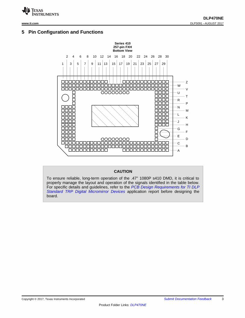
Z
V
T
P
M
K
H
F
D
B
W
U
R
N
L
J
G
E
C
A
1 3 5 7 9 11 13 15 17 19 21 23 25 27 29
2 4 6 8 10 12 14 16 18 20 22 24 26 28 30
3
DLP470NEwww.ti.com DLPS091 –AUGUST 2017
Product Folder Links: DLP470NE
Submit Documentation FeedbackCopyright © 2017, Texas Instruments Incorporated
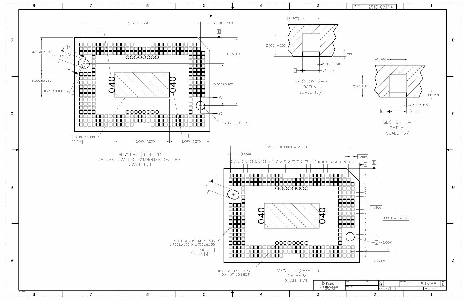
5 Pin Configuration and Functions
Series 410257-pin FXHBottom View
CAUTIONTo ensure reliable, long-term operation of the .47” 1080P s410 DMD, it is critical toproperly manage the layout and operation of the signals identified in the table below.For specific details and guidelines, refer to the PCB Design Requirements for TI DLPStandard TRP Digital Micromirror Devices application report before designing theboard.
4
DLP470NEDLPS091 –AUGUST 2017 www.ti.com
Product Folder Links: DLP470NE
Submit Documentation Feedback Copyright © 2017, Texas Instruments Incorporated
(1) The .47” 1080P TRP 2xLVDS Series 410 DMD is a component of one or more DLP chipsets. Reliable function and operation of the .47”1080P TRP 2xLVDS Series 410 DMD requires that it be used in conjunction with the other components of the applicable DLP chipset,including those components that contain or implement TI DMD control technology. TI DMD control technology is the TI technology anddevices for operating or controlling a DLP DMD.
(2) I = Input, O = Output, P = Power, G = Ground, NC = No connect
Pin Functions (1)
PINI/O (2) SIGNAL DATA
RATEINTERNAL
TERMINATION DESCRIPTIONTRACE
LENGTH(mil)NAME NO.
D_AN(0) C6
NC LVDS DDR Differential No connect 805.0
D_AN(1) C3D_AN(2) E1D_AN(3) C4D_AN(4) D1D_AN(5) B8D_AN(6) F4D_AN(7) E3D_AN(8) C11D_AN(9) F3D_AN(10) K4D_AN(11) H3D_AN(12) J3D_AN(13) C13D_AN(14) A5D_AN(15) A3D_AP(0) C7
NC LVDS DDR Differential No connect 805.0
D_AP(1) C2D_AP(2) E2D_AP(3) B4D_AP(4) C1D_AP(5) B7D_AP(6) E4D_AP(7) D3D_AP(8) C12D_AP(9) F2D_AP(10) J4D_AP(11) G3D_AP(12) J2D_AP(13) C14D_AP(14) A6D_AP(15) A4

5
DLP470NEwww.ti.com DLPS091 –AUGUST 2017
Product Folder Links: DLP470NE
Submit Documentation FeedbackCopyright © 2017, Texas Instruments Incorporated
Pin Functions(1) (continued)PIN
I/O (2) SIGNAL DATARATE
INTERNALTERMINATION DESCRIPTION
TRACELENGTH
(mil)NAME NO.
D_BN(0) N4
NC LVDS DDR Differential No connect 805.0
D_BN(1) Z11D_BN(2) W4D_BN(3) W10D_BN(4) L1D_BN(5) V8D_BN(6) W6D_BN(7) M1D_BN(8) R4D_BN(9) W1D_BN(10) U4D_BN(11) V2D_BN(12) Z5D_BN(13) N3D_BN(14) Z2D_BN(15) L4D_BP(0) M4
NC LVDS DDR Differential No connect 805.0
D_BP(1) Z12D_BP(2) Z4D_BP(3) Z10D_BP(4) L2D_BP(5) V9D_BP(6) W7D_BP(7) N1D_BP(8) P4D_BP(9) V1D_BP(10) T4D_BP(11) V3D_BP(12) Z6D_BP(13) N2D_BP(14) Z3D_BP(15) L3

6
DLP470NEDLPS091 –AUGUST 2017 www.ti.com
Product Folder Links: DLP470NE
Submit Documentation Feedback Copyright © 2017, Texas Instruments Incorporated
Pin Functions(1) (continued)PIN
I/O (2) SIGNAL DATARATE
INTERNALTERMINATION DESCRIPTION
TRACELENGTH
(mil)NAME NO.
D_CN(0) H27
I LVDS DDR Differential Data negative 805.0
D_CN(1) A20D_CN(2) H28D_CN(3) K28D_CN(4) K30D_CN(5) C23D_CN(6) G27D_CN(7) J30D_CN(8) B24D_CN(9) A21D_CN(10) A27D_CN(11) C29D_CN(12) A26D_CN(13) C25D_CN(14) A29D_CN(15) C30D_CP(0) J27
I LVDS DDR Differential Data positive 805.0
D_CP(1) A19D_CP(2) H29D_CP(3) K27D_CP(4) K29D_CP(5) C22D_CP(6) F27D_CP(7) H30D_CP(8) B25D_CP(9) B21D_CP(10) B27D_CP(11) C28D_CP(12) A25D_CP(13) C24D_CP(14) A28D_CP(15) B30

7
DLP470NEwww.ti.com DLPS091 –AUGUST 2017
Product Folder Links: DLP470NE
Submit Documentation FeedbackCopyright © 2017, Texas Instruments Incorporated
Pin Functions(1) (continued)PIN
I/O (2) SIGNAL DATARATE
INTERNALTERMINATION DESCRIPTION
TRACELENGTH
(mil)NAME NO.
D_DN(0) V25
I LVDS DDR Differential Data negative
805.0D_DN(1) V28D_DN(2) T30D_DN(3) V27D_DN(4) U30D_DN(5) W23D_DN(6) R27D_DN(7) T28D_DN(8) V20D_DN(9) R28D_DN(10) L27D_DN(11) N28D_DN(12) M28D_DN(13) V18D_DN(14) Z26D_DN(15) Z28D_DP(0) V24
I LVDS DDR Differential Data positive
805.0D_DP(1) V29D_DP(2) T29D_DP(3) W27D_DP(4) V30D_DP(5) W24D_DP(6) T27D_DP(7) U28D_DP(8) V19D_DP(9) R29D_DP(10) M27D_DP(11) P28D_DP(12) M29D_DP(13) V17D_DP(14) Z25D_DP(15) Z27SCTRL_AN G1
NC LVDS DDR Differential No connect 805.0SCTRL_AP F1SCTRL_BN V5SCTRL_BP V4SCTRL_CN C26 I LVDS DDR Differential Serial control negative 805.0SCTRL_CP C27 I LVDS DDR Differential Serial control positive 805.0SCTRL_DN P30 I LVDS DDR Differential Serial control negative 805.0SCTRL_DP R30 I LVDS DDR Differential Serial control positive 805.0
DCLK_AN H2
NC LVDS Differential No connect 805.0DCLK_AP H1DCLK_BN V6DCLK_BP V7DCLK_CN D27 I LVDS Differential Clock negative 805.0DCLK_CP E27 I LVDS Differential Clock positive 805.0

8
DLP470NEDLPS091 –AUGUST 2017 www.ti.com
Product Folder Links: DLP470NE
Submit Documentation Feedback Copyright © 2017, Texas Instruments Incorporated
Pin Functions(1) (continued)PIN
I/O (2) SIGNAL DATARATE
INTERNALTERMINATION DESCRIPTION
TRACELENGTH
(mil)NAME NO.
(3) VBIAS, VCC, VOFFSET, and VRESET power supplies must be connected for proper DMD operation.
DCLK_DN N29 I LVDS Differential Clock negative 805.0DCLK_DP N30 I LVDS Differential Clock positive 805.0
SCPCLK A10 I LVCMOS Pull down Serial communications port clock. Active onlywhen SCPENZ is logic low.
SCPDI A12 I LVCMOS SDR Pull down Serial communications port Data Input.Synchronous to SCPCLK rising edge.
SCPENZ C10 I LVCMOS Pull down Serial communications port enable active low.SCPDO A11 O LVCMOS SDR Serial communications port Output.RESET_ADDR(0) Z13
I LVCMOS Pull down Reset driver address selectRESET_ADDR(1) W13RESET_ADDR(2) V10RESET_ADDR(3) W14RESET_MODE(0) W9
I LVCMOS Pull downReset driver mode select
RESET_SEL(0) V14 Reset driver level selectRESET_SEL(1) Z8 Reset driver level select
RESET_STROBE Z9 I LVCMOS Pull down Rising edge latches in RESET_ADDR,RESET_MODE, & RESET_SEL
PWRDNZ A8 I LVCMOS Pull down Active low device reset
RESET_OEZ W15 I LVCMOS Pull up Active low Output enable for internal resetdriver circuits
RESET_IRQZ V16 O LVCMOS Active low Output interrupt to DLP displaycontroller
EN_OFFSET C9 O LVCMOS Active high enable for external VOFFSETregulator
PG_OFFSET A9 I LVCMOS Pull up Active low fault from external VOFFSETregulator
TEMP_N B18 Analog Temperature sensor diode cathodeTEMP_P B17 Analog Temperature sensor diode anode
RESERVED
D12, D13,D14, D15,D16, D17,D18, D19,U12, U13,U14, U15
NC Analog Pull DownDo not connect on DLP system board. Noconnect. No electrical connections fromCMOS bond pad to package pin.
No Connect U16, U17,U18, U19 NC No connect. No electrical connection from
CMOS bond pad to package pin.RESERVED_BA W11
O LVCMOS Do not connect on DLP system boardRESERVED_BB B11RESERVED_BC Z20RESERVED_BD C18RESERVED_PFE A18
I LVCMOS Pull down Connect to ground on DLP system board.RESERVED_TM C8RESERVED_TP0 Z19
I Analog Do not connect on DLP system boardRESERVED_TP1 W20RESERVED_TP2 W19
VBIAS (3) C15, C16,V11, V12 P Analog Supply voltage for Positive Bias level of
micromirror reset signal.
VRESET (3) G4, H4,J1, K1 P Analog Supply voltage for Negative Reset level of
micromirror reset signal

9
DLP470NEwww.ti.com DLPS091 –AUGUST 2017
Product Folder Links: DLP470NE
Submit Documentation FeedbackCopyright © 2017, Texas Instruments Incorporated
Pin Functions(1) (continued)PIN
I/O (2) SIGNAL DATARATE
INTERNALTERMINATION DESCRIPTION
TRACELENGTH
(mil)NAME NO.
(4) VSS must be connected for proper DMD operation.
VOFFSET (3)A30, B2,M30, Z1,
Z30P Analog
Supply voltage for HVCMOS logic. Supplyvoltage for positive offset level of micromirrorreset signal. Supply voltage for stepped highvoltage at micromirror address electrodes.
VCC (3)
A24, A7,B10, B13,B16, B19,B22, B28,B5, C17,C20, D4,J29, K2,L29, M2,
N27, U27,V13, V15,V22, W17,
W21,W26,
W29, W3,Z18, Z23,Z29, Z7
P Analog
Supply voltage for LVCMOS core. Supplyvoltage for positive offset level of micromirrorreset signal during Power down. Supplyvoltage for normal high level at micromirroraddress electrodes.
VSS (4)
A13, A22,A23, B12,B14, B15,B20, B23,B26, B29,
B3, B6,B9, C19,C21, C5,D2, G2,J28, K3,L28, L30,M3, P27,P29, U29,V21, V23,V26, W12,
W16,W18, W2,
W22,W25,W28,
W30, W5,W8, Z21,Z22, Z24
G Device ground. Common return for all power.

10
DLP470NEDLPS091 –AUGUST 2017 www.ti.com
Product Folder Links: DLP470NE
Submit Documentation Feedback Copyright © 2017, Texas Instruments Incorporated
(1) All voltages are referenced to common ground VSS. VBIAS, VCC, VOFFSET, and VRESET power supplies are all required for proper DMDoperation. VSS must also be connected.
(2) VOFFSET supply transients must fall within specified voltages.(3) Exceeding the recommended allowable voltage difference between VBIAS and VOFFSET may result in excessive current draw.(4) Exceeding the recommended allowable voltage difference between VBIAS and VRESET may result in excessive current draw.(5) This maximum LVDS input voltage rating applies when each input of a differential pair is at the same voltage potential.(6) LVDS differential inputs must not exceed the specified limit or damage may result to the internal termination resistors.(7) The highest temperature of the active array (as calculated using Micromirror Array Temperature Calculation) or of any point along the
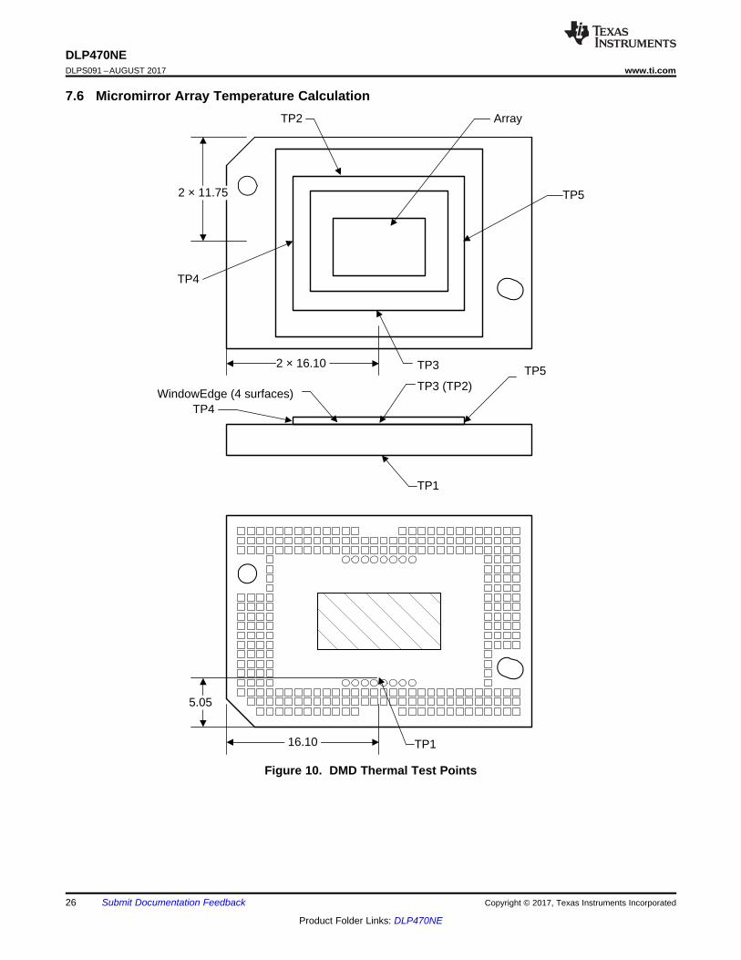
window edge as defined in Figure 10. The locations of thermal test points TP2, TP3, TP4 and TP5 in Figure 10 are intended to measurethe highest window edge temperature. If a particular application causes another point on the window edge to be at a higher temperature,that point should be used.
(8) Temperature difference is the highest difference between the ceramic test point 1 (TP1) and anywhere on the window edge as shown inFigure 10. The window test points TP2, TP3, TP4 and TP5 shown in Figure 10 are intended to result in the worst case difference. If aparticular application causes another point on the window edge to result in a larger difference temperature, that point should be used.
6 Specifications
6.1 Absolute Maximum RatingsOver operating free-air temperature range (unless otherwise noted)
MIN MAX UNITSUPPLY VOLTAGESVCC Supply voltage for LVCMOS core logic (1) –0.5 2.3 VVOFFSET Supply voltage for HVCMOS and micromirror electrode (1) (2) –0.5 11 VVBIAS Supply voltage for micromirror electrode (1) –0.5 19 VVRESET Supply voltage for micromirror electrode (1) –15 -0.3 V|VBIAS – VOFFSET| Supply voltage difference (absolute value) (3) 11 V|VBIAS – VRESET| Supply voltage difference (absolute value) (4) 34 VINPUT VOLTAGES
Input voltage for all other LVCMOS input pins (1) –0.5 VCC + 0.5 V|VID| Input differential voltage (absolute value) (5) 500 mVIID Input differential current (6) 6.3 mAClocksƒCLOCK Clock frequency for LVDS interface, DCLK_C 400 MHzƒCLOCK Clock frequency for LVDS interface, DCLK_D 400 MHzENVIRONMENTAL
TARRAY andTWINDOW
Temperature, operating (7) 0 90 °CTemperature, non–operating (7) –40 90 °C
|TDELTA| Absolute Temperature difference between any point on the window edge andthe ceramic test point TP1 (8) 30 °C
TDP Dew Point Temperature, operating and non–operating (noncondensing) 81 °C
(1) The average over time (including storage and operating) that the device is not in the elevated dew point temperature range.(2) Exposure to dew point temperatures in the elevated range during storage and operation should be limited to less than a total cumulative
time of CTELR.
6.2 Storage ConditionsApplicable for the DMD as a component or non-operating in a system
MIN MAX UNITTstg DMD storage temperature –40 80 °CTDP-AVG Average dew point temperature, (non-condensing) (1) 28 °CTDP-MAX Elevated dew point temperature range , (non-condensing) (2) 28 36 °CCTELR Cumulative time in elevated dew point temperature range 24 Months

11
DLP470NEwww.ti.com DLPS091 –AUGUST 2017
Product Folder Links: DLP470NE
Submit Documentation FeedbackCopyright © 2017, Texas Instruments Incorporated
(1) JEDEC document JEP155 states that 500-V HBM allows safe manufacturing with a standard ESD control process.(2) JEDEC document JEP157 states that 250-V CDM allows safe manufacturing with a standard ESD control process.
6.3 ESD RatingsVALUE UNIT
V(ESD)Electrostaticdischarge
Human-body model (HBM), per ANSI/ESDA/JEDEC JS-001 (1) ±2000V
Charged device model (CDM), per JEDEC specification JESD22-C101 (2) ±500
(1) All voltages are referenced to common ground VSS. VBIAS, VCC, VOFFSET, and VRESET power supplies are all required for properDMD operation. VSS must also be connected.
(2) VOFFSET supply transients must fall within specified max voltages.(3) To prevent excess current, the supply voltage difference |VBIAS – VOFFSET| must be less than specified limit. See Power Supply
Recommendations, Figure 13, and Table 8.(4) To prevent excess current, the supply voltage difference |VBIAS – VRESET| must be less than specified limit. See Power Supply
Recommendations, Figure 13, and Table 8.(5) Low-speed interface is LPSDR and adheres to the Electrical Characteristics and AC/DC Operating Conditions table in JEDEC Standard
No. 209B, “Low-Power Double Data Rate (LPDDR)” JESD209B.Tester Conditions for VIH and VIL.(a) Frequency = 60 MHz. Maximum Rise Time = 2.5 ns @ (20% - 80%)(b) Frequency = 60 MHz. Maximum Fall Time = 2.5 ns @ (80% - 20%)
(6) PWRDNZ input pin resets the SCP and disables the LVDS receivers. PWRDNZ input pin overrides SCPENZ input pin and tristates theSCPDO output pin.
(7) The SCP clock is a gated clock. Duty cycle must be 50% ± 10%. SCP parameter is related to the frequency of DCLK.(8) See Figure 2.
6.4 Recommended Operating ConditionsOver operating free-air temperature range (unless otherwise noted). The functional performance of the device specified in thisdata sheet is achieved when operating the device within the limits defined by this table. No level of performance is impliedwhen operating the device above or below these limits.
MIN NOM MAX UNITVOLTAGE SUPPLYVCC LVCMOS logic supply voltage (1) 1.65 1.8 1.95 VVOFFSET Mirror electrode and HVCMOS voltage (1) (2) 9.5 10 10.5 VVBIAS Mirror electrode voltage (1) 17.5 18 18.5 VVRESET Mirror electrode voltage (1) –14.5 –14 –13.5 V|VBIAS –VOFFSET| Supply voltage difference (absolute value) (3) 10.5 V
|VBIAS – VRESET| Supply voltage difference (absolute value) (4) 33 VLVCMOS INTERFACEVIH(DC) DC input high voltage (5) 0.7 × VCC VCC + 0.3 VVIL(DC) DC input low voltage (5) –0.3 0.3 × VCC VVIH(AC) AC input high voltage (5) 0.8 × VCC VCC + 0.3 VVIL(AC) AC input low voltage (5) –0.3 0.2 × VCC VtPWRDNZ PWRDNZ pulse duration (6) 10 nsSCP INTERFACEƒSCPCLK SCP clock frequency (7) 500 kHz
tSCP_PDPropagation delay, Clock to Q, from rising–edge of SCPCLK to validSCPDO (8) 0 900 ns
tSCP_NEG_ENZTime between falling-edge of SCPENZ and the first rising- edge ofSCPCLK 1 µs
tSCP_POS_ENZ Time between falling-edge of SCPCLK and the rising-edge of SCPENZ 1 µstSCP_DS SCPDI Clock setup time (before SCPCLK falling edge) (8) 800 nstSCP_DH SCPDI Hold time (after SCPCLK falling edge) (8) 900 nstSCP_PW_ENZ SCPENZ inactive pulse duration (high level) 2 µs

12
DLP470NEDLPS091 –AUGUST 2017 www.ti.com
Product Folder Links: DLP470NE
Submit Documentation Feedback Copyright © 2017, Texas Instruments Incorporated
Recommended Operating Conditions (continued)Over operating free-air temperature range (unless otherwise noted). The functional performance of the device specified in thisdata sheet is achieved when operating the device within the limits defined by this table. No level of performance is impliedwhen operating the device above or below these limits.
MIN NOM MAX UNIT
(9) See LVDS Timing Requirements in Timing Requirements and Figure 6.(10) See Figure 5 LVDS Waveform Requirements.(11) Simultaneous exposure of the DMD to the maximum Recommended Operating Conditions for temperature and UV illumination reduces
device lifetime.(12) The array temperature cannot be measured directly and must be computed analytically from the temperature measured at test point 1
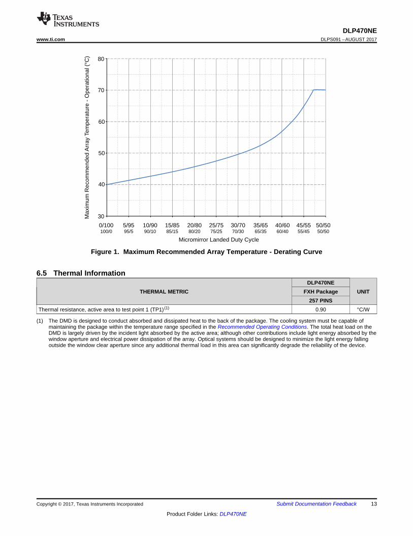
(TP1) shown in Figure 10 and the package thermal resistance Micromirror Array Temperature Calculation.(13) Per Figure 1, the maximum operational array temperature should be derated based on the micromirror landed duty cycle that the DMD
experiences in the end application. See Micromirror Landed-On/Landed-Off Duty Cycle for a definition of micromirror landed duty cycle.(14) Long-term is defined as the usable life of the device.(15) Array temperatures beyond those specified as long-term are recommended for short-term conditions only (power-up). Short-term is
defined as cumulative time over the usable life of the device and is less than 500 hours.(16) The maximum marginal ray angle of the incoming illumination light at any point in the micromirror array, including Pond of Micromirrors
(POM), should not exceed 55 degrees from the normal to the device array plane. The device window aperture has not necessarily beendesigned to allow incoming light at higher maximum angles to pass to the micromirrors, and the device performance has not been testednor qualified at angles exceeding this. Illumination light exceeding this angle outside the micromirror array (including POM) willcontribute to thermal limitations described in this document, and may negatively affect lifetime.
(17) Temperature difference is the highest difference between the ceramic test point 1 (TP1) and anywhere on the window edge as shownin Figure 10. The window test points TP2, TP3, TP4 and TP5 shown in Figure 10 are intended to result in the worst case differencetemperature. If a particular application causes another point on the window edge to result in a larger difference in temperature, that pointshould be used.
(18) DMD is qualified at the combination of the maximum temperature and maximum lumens specified. Operation of the DMD outside ofthese limits has not been tested.
(19) The average over time (including storage and operating) that the device is not in the ‘elevated dew point temperature range.(20) Exposure to dew point temperatures in the elevated range during storage and operation should be limited to less than a total
cumulative time of CTELR.
LVDS INTERFACEƒCLOCK Clock frequency for LVDS interface (all channels), DCLK (9) 400 MHz|VID| Input differential voltage (absolute value) (10) 150 300 440 mVVCM Common mode voltage (10) 1100 1200 1300 mVVLVDS LVDS voltage (10) 880 1520 mVtLVDS_RSTZ Time required for LVDS receivers to recover from PWRDNZ 2000 nsZIN Internal differential termination resistance 80 100 120 Ω
ZLINE Line differential impedance (PWB/trace) 90 100 110 Ω
ENVIRONMENTAL
TARRAYArray temperature, Long–term operational (11) (12) (13) (14) 10 40 to
70 (13) °C
Array temperature, Short–term operational (12) (15) 0 10 °CTWINDOW Window temperature – operational (16) 85 °C
|TDELTA| Absolute temperature difference between any point on the windowedge and the ceramic test point TP1 (17) (18) 14 °C
TDP -AVG Average dew point average temperature (non–condensing) (19) 28 °CTDP-MAX Elevated dew point temperature range (non-condensing) (20) 28 36 °CCTELR Cumulative time in elevated dew point temperature range 24 MonthsL Operating system luminance (18) 4000 lmILLUV Illumination Wavelengths < 395 nm (11) 0.68 2.00 mW/cm2
ILLVIS Illumination Wavelengths between 395 nm and 800 nm Thermally limited mW/cm2
ILLIR Illumination Wavelengths > 800 nm 10 mW/cm2
ILLθ Illumination Marginal Ray Angle (16) 55 deg
0/100 100/0
30
5/95 95/5
40
50
60
70
80
10/90 90/10
15/85 85/15
20/80 80/20
25/75 75/25
30/70 70/30
35/65 65/35
40/60 60/40
45/55 55/45
50/50 50/50
Micromirror Landed Duty Cycle
Max
imum
Rec
omm
ende
d A
rray
Tem
pera
ture
- O
pera
tiona
l (¹C
)
13
DLP470NEwww.ti.com DLPS091 –AUGUST 2017
Product Folder Links: DLP470NE
Submit Documentation FeedbackCopyright © 2017, Texas Instruments Incorporated
(1) The DMD is designed to conduct absorbed and dissipated heat to the back of the package. The cooling system must be capable ofmaintaining the package within the temperature range specified in the Recommended Operating Conditions. The total heat load on theDMD is largely driven by the incident light absorbed by the active area; although other contributions include light energy absorbed by thewindow aperture and electrical power dissipation of the array. Optical systems should be designed to minimize the light energy fallingoutside the window clear aperture since any additional thermal load in this area can significantly degrade the reliability of the device.
Figure 1. Maximum Recommended Array Temperature - Derating Curve
6.5 Thermal Information
THERMAL METRICDLP470NE
UNITFXH Package257 PINS
Thermal resistance, active area to test point 1 (TP1) (1) 0.90 °C/W

14
DLP470NEDLPS091 –AUGUST 2017 www.ti.com
Product Folder Links: DLP470NE
Submit Documentation Feedback Copyright © 2017, Texas Instruments Incorporated
(1) Applies to LVCMOS pins only. Excludes LVDS pins and MBRST (15:0) pins.(2) To prevent excess current, the supply voltage difference |VBIAS – VOFFSET| must be less than the specified limits listed in the
Recommended Operating Conditions table.(3) To prevent excess current, the supply voltage difference |VBIAS – VRESET| must be less than specified limit in Recommended
Operating Conditions.
6.6 Electrical CharacteristicsOver operating free-air temperature range (unless otherwise noted)
PARAMETER TEST CONDITIONS MIN TYP MAX UNITVOH High level output voltage VCC = 1.8 V, IOH = –2 mA 0.8 x VCC VVOL Low level output voltage VCC = 1.95 V, IOL = 2 mA 0.2 x VCC VIOZ High impedance output current VCC = 1.95 V –40 25 µAIIL Low level input current VCC = 1.95 V, VI = 0 –1 µAIIH High level input current (1) (2) VCC = 1.95 V, VI = VCC 110 µAICC Supply current VCC VCC = 1.95 V 715 mAIOFFSET Supply current VOFFSET (2) VOFFSET = 10.5 V 7 mAIBIAS Supply current VBIAS (2) (3) VBIAS = 18.5 V 2.75 mAIRESET Supply current VRESET (3) VRESET = –14.5 V -5 mAPCC Supply power dissipation VCC VCC = 1.95 V 1394.25 mW
POFFSETSupply power dissipationVOFFSET
(2) VOFFSET = 10.5 V 73.50 mW
PBIASSupply power dissipationVBIAS
(2) (3) VBIAS = 18.5 V 50.87 mW
PRESETSupply power dissipationVRESET
(3) VRESET = –14.5 V 72.5 mW
PTOTALSupply power dissipationVTOTAL
1591.12 mW
6.7 Capacitance at Recommended Operating Conditionsover operating free-air temperature range (unless otherwise noted)
PARAMETER TEST CONDITIONS MIN TYP MAX UNITCI_lvds LVDS input capacitance 2× LVDS ƒ = 1 MHz 20 pF
CI_nonlvdsNon-LVDS input capacitance 2×LVDS ƒ = 1 MHz 20 pF
CI_tdiodeTemperature diode inputcapacitance 2× LVDS ƒ = 1 MHz 30 pF
CO Output capacitance ƒ = 1 MHz 20 pF
xxxxxx
SCPENZ
SCPCLK
SCPDI
SCPDO
DI
t SCP_NEG_ENZ
t SCP_DS
xxxx
xxxxxxxx
DO
50%
50%
tC
fSCPCLK= 1 / t C
tSCP_PD
Falling Edge Capture for SCPDIRising Edge Launch for SCPDO
xxxx
50% 50%
50%
50%
50% 50%
50%
t SCP_DH
tSCP_POS_ENZ
15
DLP470NEwww.ti.com DLPS091 –AUGUST 2017
Product Folder Links: DLP470NE
Submit Documentation FeedbackCopyright © 2017, Texas Instruments Incorporated
(1) See Figure 3 for Rise Time and Fall Time for SCP.(2) See Figure 5 for Timing Requirements for LVDS.(3) Channel C (Bus C) includes the following LVDS pairs: DCLK_CN and DCLK_CP, SCTRL_CN and SCTRL_CP, D_CN(15:0) and
D_CP(15:0).(4) Channel D (Bus D) includes the following LVDS pairs: DCLK_DN and DCLK_DP, SCTRL_DN and SCTRL_DP, D_DN(15:0) and
D_DP(15:0).
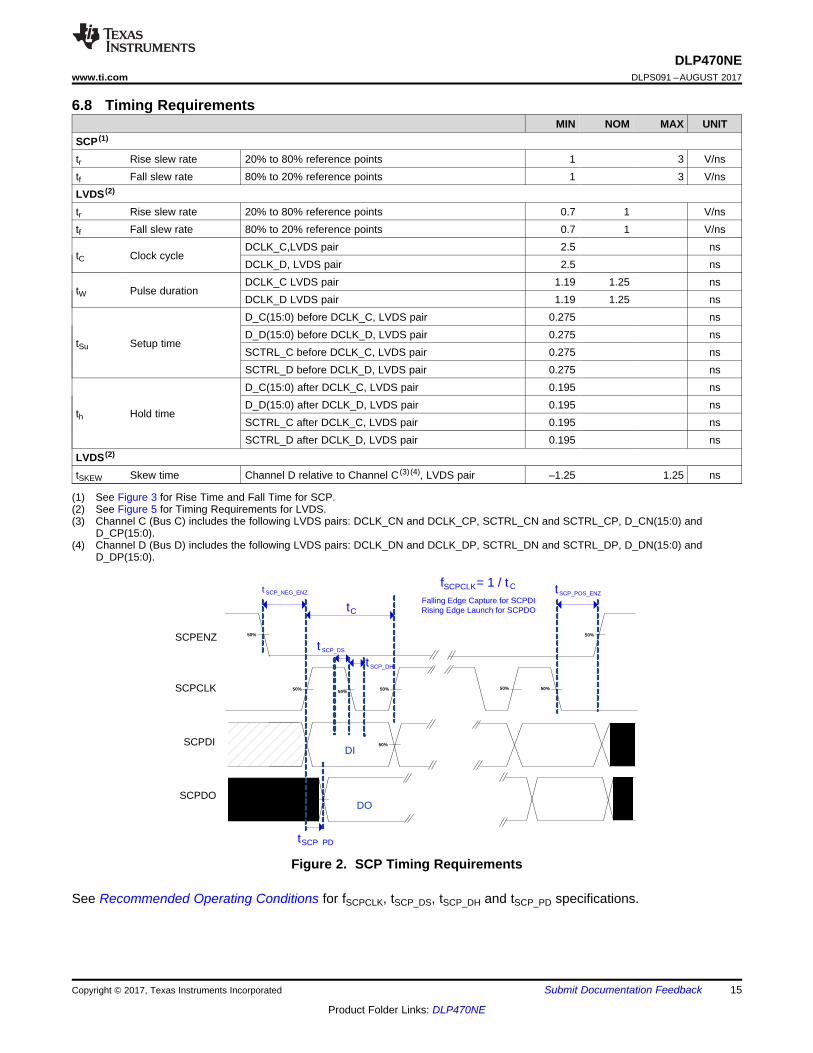
6.8 Timing RequirementsMIN NOM MAX UNIT
SCP (1)
tr Rise slew rate 20% to 80% reference points 1 3 V/nstf Fall slew rate 80% to 20% reference points 1 3 V/nsLVDS (2)
tr Rise slew rate 20% to 80% reference points 0.7 1 V/nstf Fall slew rate 80% to 20% reference points 0.7 1 V/ns
tC Clock cycleDCLK_C,LVDS pair 2.5 nsDCLK_D, LVDS pair 2.5 ns
tW Pulse durationDCLK_C LVDS pair 1.19 1.25 nsDCLK_D LVDS pair 1.19 1.25 ns
tSu Setup time
D_C(15:0) before DCLK_C, LVDS pair 0.275 nsD_D(15:0) before DCLK_D, LVDS pair 0.275 nsSCTRL_C before DCLK_C, LVDS pair 0.275 nsSCTRL_D before DCLK_D, LVDS pair 0.275 ns
th Hold time
D_C(15:0) after DCLK_C, LVDS pair 0.195 nsD_D(15:0) after DCLK_D, LVDS pair 0.195 nsSCTRL_C after DCLK_C, LVDS pair 0.195 nsSCTRL_D after DCLK_D, LVDS pair 0.195 ns
LVDS (2)
tSKEW Skew time Channel D relative to Channel C (3) (4), LVDS pair –1.25 1.25 ns
Figure 2. SCP Timing Requirements
See Recommended Operating Conditions for fSCPCLK, tSCP_DS, tSCP_DH and tSCP_PD specifications.
VCM VID
tr
tfVLVDS max = VCM max + | 1/2 * VID max |
VLVDS min = VCM min ± | 1/2 * VID max |
CLOAD
Tester channelDevice pin
output under test
0
VCC
Not to Scale tf. tr.Time
Vol
tage
(V
)
16
DLP470NEDLPS091 –AUGUST 2017 www.ti.com
Product Folder Links: DLP470NE
Submit Documentation Feedback Copyright © 2017, Texas Instruments Incorporated
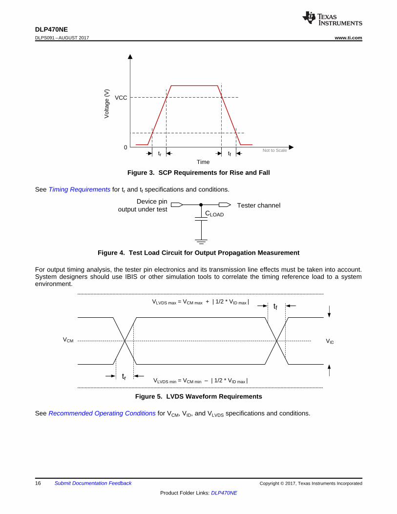
Figure 3. SCP Requirements for Rise and Fall
See Timing Requirements for tr and tf specifications and conditions.
Figure 4. Test Load Circuit for Output Propagation Measurement
For output timing analysis, the tester pin electronics and its transmission line effects must be taken into account.System designers should use IBIS or other simulation tools to correlate the timing reference load to a systemenvironment.
Figure 5. LVDS Waveform Requirements
See Recommended Operating Conditions for VCM, VID, and VLVDS specifications and conditions.
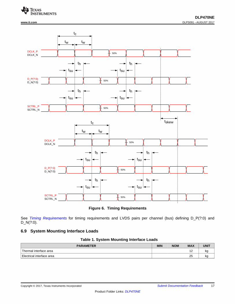
tc
DCLK_NDCLK_P
D_N(?:0)D_P(?:0)
tw tw
th
tsu
th
tsu
50%
50%
SCTRL_NSCTRL_P
th
tsu
th
tsu
50%
tc
DCLK_NDCLK_P
D_N(?:0)D_P(?:0)
tw tw
th
tsu
th
tsu
50%
50%
SCTRL_NSCTRL_P
th
tsu
th
tsu
50%
tskew
17
DLP470NEwww.ti.com DLPS091 –AUGUST 2017
Product Folder Links: DLP470NE
Submit Documentation FeedbackCopyright © 2017, Texas Instruments Incorporated
Figure 6. Timing Requirements
See Timing Requirements for timing requirements and LVDS pairs per channel (bus) defining D_P(?:0) andD_N(?:0).
6.9 System Mounting Interface Loads
Table 1. System Mounting Interface LoadsPARAMETER MIN NOM MAX UNIT
Thermal interface area 12 kgElectrical interface area 25 kg
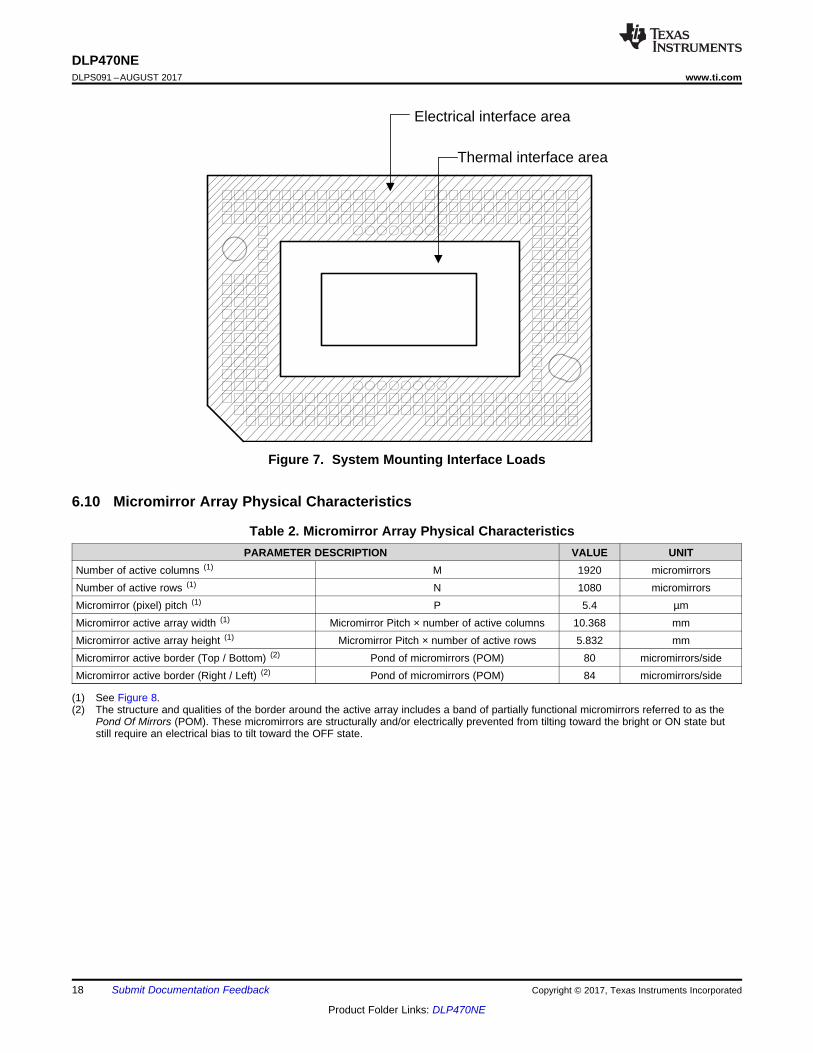
Electrical interface area
Thermal interface area
18
DLP470NEDLPS091 –AUGUST 2017 www.ti.com
Product Folder Links: DLP470NE
Submit Documentation Feedback Copyright © 2017, Texas Instruments Incorporated
(1) See Figure 8.(2) The structure and qualities of the border around the active array includes a band of partially functional micromirrors referred to as the
Pond Of Mirrors (POM). These micromirrors are structurally and/or electrically prevented from tilting toward the bright or ON state butstill require an electrical bias to tilt toward the OFF state.
Figure 7. System Mounting Interface Loads
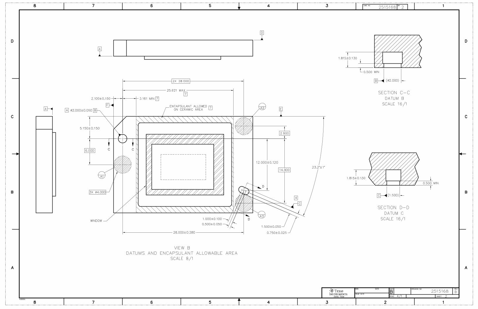
6.10 Micromirror Array Physical Characteristics
Table 2. Micromirror Array Physical CharacteristicsPARAMETER DESCRIPTION VALUE UNIT
Number of active columns (1) M 1920 micromirrorsNumber of active rows (1) N 1080 micromirrorsMicromirror (pixel) pitch (1) P 5.4 µmMicromirror active array width (1) Micromirror Pitch × number of active columns 10.368 mmMicromirror active array height (1) Micromirror Pitch × number of active rows 5.832 mmMicromirror active border (Top / Bottom) (2) Pond of micromirrors (POM) 80 micromirrors/sideMicromirror active border (Right / Left) (2) Pond of micromirrors (POM) 84 micromirrors/side

N ± 1
0 1 2
012
M ±
1
Active Micromirror Array
3
N ± 4
3 M ±
2
M ±
3
M ±
4
N ± 2N ± 3
M x P
N x PM x N Micromirrors
P P
P
Pond Of Micromirrors (POM) omitted for clarity.
Not to scale.
P
Details omitted for clarity.
Off-StateLight Path
IncidentIlluminationLight Path
19
DLP470NEwww.ti.com DLPS091 –AUGUST 2017
Product Folder Links: DLP470NE
Submit Documentation FeedbackCopyright © 2017, Texas Instruments Incorporated
Figure 8. Micromirror Array Physical Characteristics
Refer to section Micromirror Array Physical Characteristics table for M, N, and P specifications.
N ± 1
0 1 2
012
M ±
1
3
N ± 4
3 M ±
2
M ±
3
M ±
4
N ± 2N ± 3
Border micromirrors omitted for clarity
Details omitted for clarity.
Tilted Axis of Pixel Rotation
On-State Landed Edge
Off-State Landed Edge
Off State Light Path
IncidentIlluminationLight Path
Not to scale.
20
DLP470NEDLPS091 –AUGUST 2017 www.ti.com
Product Folder Links: DLP470NE
Submit Documentation Feedback Copyright © 2017, Texas Instruments Incorporated
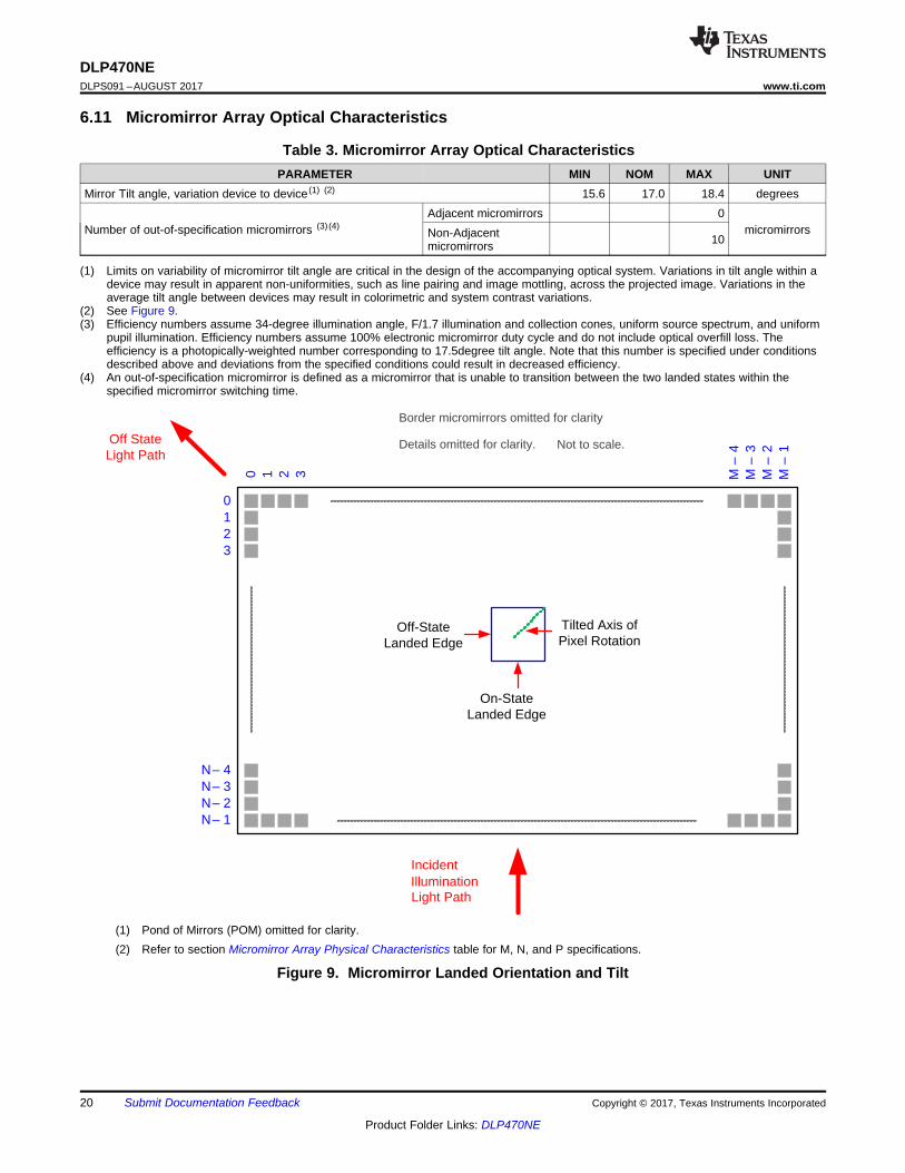
(1) Limits on variability of micromirror tilt angle are critical in the design of the accompanying optical system. Variations in tilt angle within adevice may result in apparent non-uniformities, such as line pairing and image mottling, across the projected image. Variations in theaverage tilt angle between devices may result in colorimetric and system contrast variations.
(2) See Figure 9.(3) Efficiency numbers assume 34-degree illumination angle, F/1.7 illumination and collection cones, uniform source spectrum, and uniform
pupil illumination. Efficiency numbers assume 100% electronic micromirror duty cycle and do not include optical overfill loss. Theefficiency is a photopically-weighted number corresponding to 17.5degree tilt angle. Note that this number is specified under conditionsdescribed above and deviations from the specified conditions could result in decreased efficiency.
(4) An out-of-specification micromirror is defined as a micromirror that is unable to transition between the two landed states within thespecified micromirror switching time.
6.11 Micromirror Array Optical Characteristics
Table 3. Micromirror Array Optical CharacteristicsPARAMETER MIN NOM MAX UNIT
Mirror Tilt angle, variation device to device (1) (2) 15.6 17.0 18.4 degrees
Number of out-of-specification micromirrors (3) (4)Adjacent micromirrors 0
micromirrorsNon-Adjacentmicromirrors 10
(1) Pond of Mirrors (POM) omitted for clarity.(2) Refer to section Micromirror Array Physical Characteristics table for M, N, and P specifications.
Figure 9. Micromirror Landed Orientation and Tilt
21
DLP470NEwww.ti.com DLPS091 –AUGUST 2017
Product Folder Links: DLP470NE
Submit Documentation FeedbackCopyright © 2017, Texas Instruments Incorporated
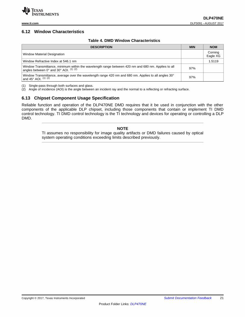
(1) Single-pass through both surfaces and glass.(2) Angle of incidence (AOI) is the angle between an incident ray and the normal to a reflecting or refracting surface.
6.12 Window Characteristics
Table 4. DMD Window CharacteristicsDESCRIPTION MIN NOM
Window Material Designation CorningEagle XG
Window Refractive Index at 546.1 nm 1.5119Window Transmittance, minimum within the wavelength range between 420 nm and 680 nm. Applies to allangles between 0° and 30° AOI. (1) (2) 97%
Window Transmittance, average over the wavelength range 420 nm and 680 nm. Applies to all angles 30°and 45° AOI. (1) (2) 97%
6.13 Chipset Component Usage SpecificationReliable function and operation of the DLP470NE DMD requires that it be used in conjunction with the othercomponents of the applicable DLP chipset, including those components that contain or implement TI DMDcontrol technology. TI DMD control technology is the TI technology and devices for operating or controlling a DLPDMD.
NOTETI assumes no responsibility for image quality artifacts or DMD failures caused by opticalsystem operating conditions exceeding limits described previously.
22
DLP470NEDLPS091 –AUGUST 2017 www.ti.com
Product Folder Links: DLP470NE
Submit Documentation Feedback Copyright © 2017, Texas Instruments Incorporated
7 Detailed Description
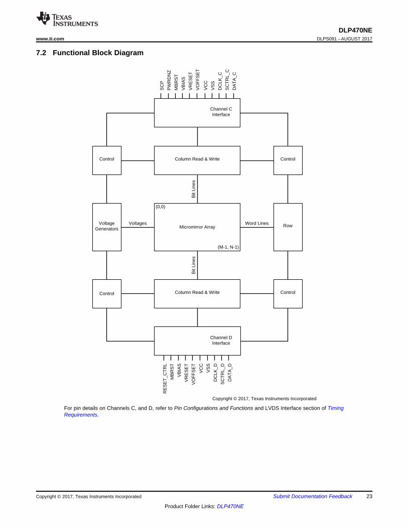
7.1 OverviewThe DMD is a 0.47 inch diagonal spatial light modulator which consists of an array of highly reflective aluminummicromirrors. The DMD is an electrical input, optical output micro-optical-electrical-mechanical system (MEMS).The electrical interface is Low Voltage Differential Signaling (LVDS). The DMD consists of a two-dimensionalarray of 1-bit CMOS memory cells. The array is organized in a grid of M memory cell columns by N memory cellrows. Refer to the Functional Block Diagram. The positive or negative deflection angle of the micromirrors can beindividually controlled by changing the address voltage of underlying CMOS addressing circuitry and micromirrorreset signals (MBRST).
The DLP470NE DMD is part of the chipset comprising of the DLP470NE DMD, the DLPC4422 display controllerand the DLPA100 power and motor driver. To ensure reliable operation, the DLP470NE DMD must always beused with the DLPC4422 display controller and the DLPA100 power and motor driver.
Column Read & Write
Bit
Line
s
Word Lines
(0,0)
(M-1, N-1)
Micromirror Array
Control
VoltageGenerators
Control
Control Control
Bit
Line
s
Row
Column Read & Write
Voltages
Channel CInterface
Channel DInterface
DA
TA
_C
SC
TR
L_C
DC
LK_C
DA
TA
_D
SC
TR
L_D
DC
LK_D
VS
S
VC
C
VO
FF
SE
T
VR
ES
ET
VB
IAS
VS
S
VC
C
VO
FF
SE
T
VR
ES
ET
VB
IAS
MB
RS
TM
BR
ST
SC
PR
ES
ET
_CT
RL
PW
RD
NZ
Copyright © 2017, Texas Instruments Incorporated
23
DLP470NEwww.ti.com DLPS091 –AUGUST 2017
Product Folder Links: DLP470NE
Submit Documentation FeedbackCopyright © 2017, Texas Instruments Incorporated
7.2 Functional Block Diagram
For pin details on Channels C, and D, refer to Pin Configurations and Functions and LVDS Interface section of TimingRequirements.
24
DLP470NEDLPS091 –AUGUST 2017 www.ti.com
Product Folder Links: DLP470NE
Submit Documentation Feedback Copyright © 2017, Texas Instruments Incorporated
7.3 Feature Description
7.3.1 Power InterfaceThe DMD requires 5 DC voltages: DMD_P3P3V, DMD_P1P8V, VOFFSET, VRESET, and VBIAS. DMD_P3P3Vis created by the DLPA100 power and motor driver and is used on the DMD board to create the other 4 DMDvoltages, as well as powering various peripherals (TMP411, I2C, and TI level translators). DMD_P1P8V iscreated by the TI PMIC LP38513S and provides the VCC voltage required by the DMD. VOFFSET (10V),VRESET (-14V), and VBIAS(18V) are made by the TI PMIC TPS65145 and are supplied to the DMD to controlthe micromirrors.
7.3.2 TimingThe data sheet provides timing at the device pin. For output timing analysis, the tester pin electronics and itstransmission line effects must be taken into account. Figure 4 shows an equivalent test load circuit for the outputunder test. Timing reference loads are not intended as a precise representation of any particular systemenvironment or depiction of the actual load presented by a production test. System designers should use IBIS orother simulation tools to correlate the timing reference load to a system environment. The load capacitance valuestated is only for characterization and measurement of AC timing signals. This load capacitance value does notindicate the maximum load the device is capable of driving.
7.4 Device Functional ModesDMD functional modes are controlled by the DLPC4422 display controller. See the DLPC4422 display controllerdata sheet or contact a TI applications engineer.
7.5 Window Characteristics and Optics
7.5.1 Optical Interface and System Image QualityTI assumes no responsibility for end-equipment optical performance. Achieving the desired end-equipmentoptical performance involves making trade-offs between numerous component and system design parameters.Optimizing system optical performance and image quality strongly relate to optical system design parametertrades. Although it is not possible to anticipate every conceivable application, projector image quality and opticalperformance is contingent on compliance to the optical system operating conditions described in the followingsections.
7.5.1.1 Numerical Aperture and Stray Light ControlThe angle defined by the numerical aperture of the illumination and projection optics at the DMD optical areashould be the same. This angle should not exceed the nominal device micromirror tilt angle unless appropriateapertures are added in the illumination and/or projection pupils to block out flat-state and stray light from theprojection lens. The micromirror tilt angle defines DMD capability to separate the "ON" optical path from anyother light path, including undesirable flat-state specular reflections from the DMD window, DMD borderstructures, or other system surfaces near the DMD such as prism or lens surfaces. If the numerical apertureexceeds the micromirror tilt angle, or if the projection numerical aperture angle is more than two degrees largerthan the illumination numerical aperture angle, objectionable artifacts in the display border and/or active areacould occur.
7.5.1.2 Pupil MatchTI’s optical and image quality specifications assume that the exit pupil of the illumination optics is nominallycentered within 2° of the entrance pupil of the projection optics. Misalignment of pupils can create objectionableartifacts in the display border and/or active area, which may require additional system apertures to control,especially if the numerical aperture of the system exceeds the pixel tilt angle.
25
DLP470NEwww.ti.com DLPS091 –AUGUST 2017
Product Folder Links: DLP470NE
Submit Documentation FeedbackCopyright © 2017, Texas Instruments Incorporated
Window Characteristics and Optics (continued)7.5.1.3 Illumination OverfillThe active area of the device is surrounded by an aperture on the inside DMD window surface that masksstructures of the DMD chip assembly from normal view, and is sized to anticipate several optical operatingconditions. Overfill light illuminating the window aperture can create artifacts from the edge of the windowaperture opening and other surface anomalies that may be visible on the screen. The illumination optical systemshould be designed to limit light flux incident anywhere on the window aperture from exceeding approximately10% of the average flux level in the active area. Depending on the particular system optical architecture, overfilllight may have to be further reduced below the suggested 10% level in order to be acceptable.
16.10.
5.05
TP5
2 × 11.75
TP4
TP5
ArrayTP2
TP32 × 16.10.
WindowEdge (4 surfaces)TP4
TP1
TP3 (TP2)
TP1
26
DLP470NEDLPS091 –AUGUST 2017 www.ti.com
Product Folder Links: DLP470NE
Submit Documentation Feedback Copyright © 2017, Texas Instruments Incorporated
7.6 Micromirror Array Temperature Calculation
Figure 10. DMD Thermal Test Points
27
DLP470NEwww.ti.com DLPS091 –AUGUST 2017
Product Folder Links: DLP470NE
Submit Documentation FeedbackCopyright © 2017, Texas Instruments Incorporated
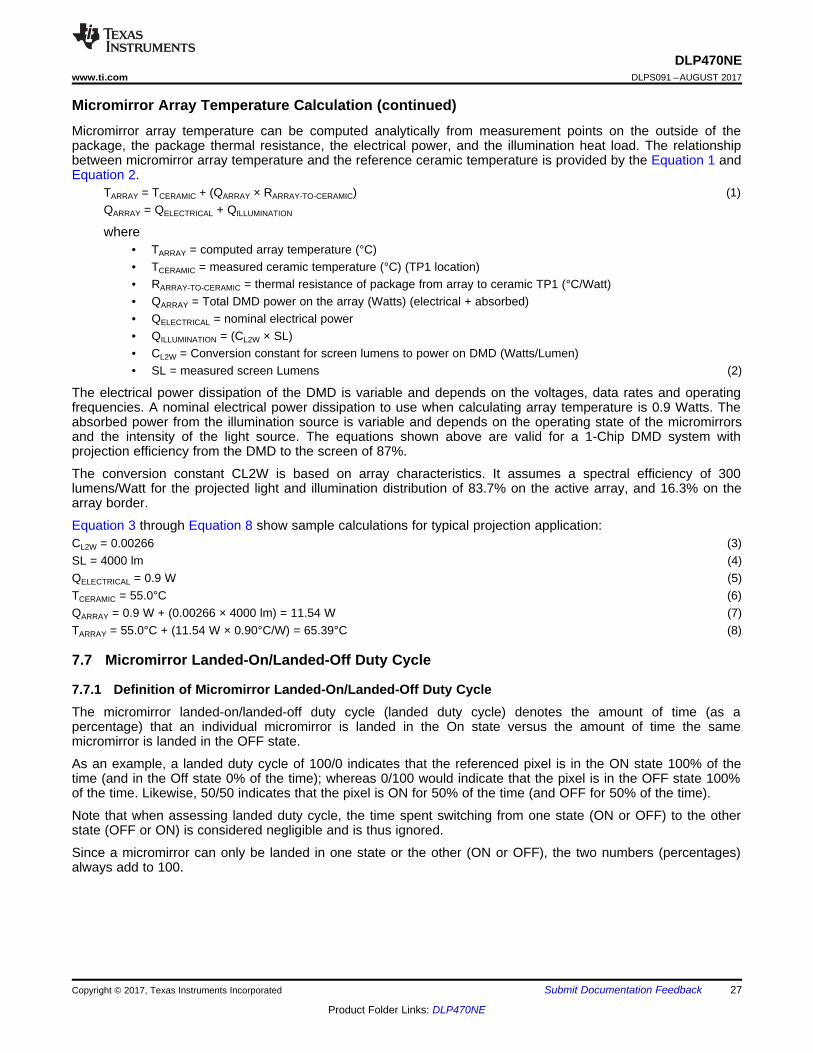
Micromirror Array Temperature Calculation (continued)Micromirror array temperature can be computed analytically from measurement points on the outside of thepackage, the package thermal resistance, the electrical power, and the illumination heat load. The relationshipbetween micromirror array temperature and the reference ceramic temperature is provided by the Equation 1 andEquation 2.
TARRAY = TCERAMIC + (QARRAY × RARRAY-TO-CERAMIC) (1)QARRAY = QELECTRICAL + QILLUMINATION
where• TARRAY = computed array temperature (°C)• TCERAMIC = measured ceramic temperature (°C) (TP1 location)• RARRAY-TO-CERAMIC = thermal resistance of package from array to ceramic TP1 (°C/Watt)• QARRAY = Total DMD power on the array (Watts) (electrical + absorbed)• QELECTRICAL = nominal electrical power• QILLUMINATION = (CL2W × SL)• CL2W = Conversion constant for screen lumens to power on DMD (Watts/Lumen)• SL = measured screen Lumens (2)
The electrical power dissipation of the DMD is variable and depends on the voltages, data rates and operatingfrequencies. A nominal electrical power dissipation to use when calculating array temperature is 0.9 Watts. Theabsorbed power from the illumination source is variable and depends on the operating state of the micromirrorsand the intensity of the light source. The equations shown above are valid for a 1-Chip DMD system withprojection efficiency from the DMD to the screen of 87%.
The conversion constant CL2W is based on array characteristics. It assumes a spectral efficiency of 300lumens/Watt for the projected light and illumination distribution of 83.7% on the active array, and 16.3% on thearray border.
Equation 3 through Equation 8 show sample calculations for typical projection application:CL2W = 0.00266 (3)SL = 4000 lm (4)QELECTRICAL = 0.9 W (5)TCERAMIC = 55.0°C (6)QARRAY = 0.9 W + (0.00266 × 4000 lm) = 11.54 W (7)TARRAY = 55.0°C + (11.54 W × 0.90°C/W) = 65.39°C (8)
7.7 Micromirror Landed-On/Landed-Off Duty Cycle
7.7.1 Definition of Micromirror Landed-On/Landed-Off Duty CycleThe micromirror landed-on/landed-off duty cycle (landed duty cycle) denotes the amount of time (as apercentage) that an individual micromirror is landed in the On state versus the amount of time the samemicromirror is landed in the OFF state.
As an example, a landed duty cycle of 100/0 indicates that the referenced pixel is in the ON state 100% of thetime (and in the Off state 0% of the time); whereas 0/100 would indicate that the pixel is in the OFF state 100%of the time. Likewise, 50/50 indicates that the pixel is ON for 50% of the time (and OFF for 50% of the time).
Note that when assessing landed duty cycle, the time spent switching from one state (ON or OFF) to the otherstate (OFF or ON) is considered negligible and is thus ignored.
Since a micromirror can only be landed in one state or the other (ON or OFF), the two numbers (percentages)always add to 100.

28
DLP470NEDLPS091 –AUGUST 2017 www.ti.com
Product Folder Links: DLP470NE
Submit Documentation Feedback Copyright © 2017, Texas Instruments Incorporated
Micromirror Landed-On/Landed-Off Duty Cycle (continued)7.7.2 Landed Duty Cycle and Useful Life of the DMDKnowing the long-term average landed duty cycle (of the end product or application) is important becausesubjecting all (or a portion) of the DMD micromirror array (also called the active array) to an asymmetric landedduty cycle for a prolonged period of time can reduce the DMD usable life.
Note that it is the symmetry/asymmetry of the landed duty cycle that is of relevance. The symmetry of the landedduty cycle is determined by how close the two numbers (percentages) are to being equal. For example, a landedduty cycle of 50/50 is perfectly symmetrical whereas a landed duty cycle of 100/0 or 0/100 is perfectlyasymmetrical.
7.7.3 Landed Duty Cycle and Operational DMD TemperatureOperational DMD temperature and landed duty cycle interact to affect DMD usable life, and this interaction canbe exploited to reduce the impact that an asymmetrical landed duty cycle has on the DMD usable life. This isquantified in the de-rating curve shown in Figure 1. The importance of this curve is that:• All points along this curve represent the same usable life.• All points above this curve represent lower usable life (and the further away from the curve, the lower the
usable life).• All points below this curve represent higher usable life (and the further away from the curve, the higher the
usable life).
In practice, this curve specifies the Maximum Operating DMD Temperature that the DMD should be operated atfor a given long-term average Landed Duty Cycle.
7.7.4 Estimating the Long-Term Average Landed Duty Cycle of a Product or ApplicationDuring a given period of time, the Landed Duty Cycle of a given pixel follows from the image content beingdisplayed by that pixel.
For example, in the simplest case, when displaying pure-white on a given pixel for a given time period, that pixeloperates under a 100/0 Landed Duty Cycle during that time period. Likewise, when displaying pure-black, thepixel operates under a 0/100 Landed Duty Cycle.
Between the two extremes (ignoring for the moment color and any image processing that may be applied to anincoming image), the Landed Duty Cycle tracks one-to-one with the gray scale value, as shown in Table 5.
Table 5. Grayscale Value and Landed Duty CycleGRAYSCALE VALUE LANDED DUTY CYCLE
0% 0/10010% 10/9020% 20/8030% 30/7040% 40/6050% 50/5060% 60/4070% 70/3080% 80/2090% 90/10100% 100/0

29
DLP470NEwww.ti.com DLPS091 –AUGUST 2017
Product Folder Links: DLP470NE
Submit Documentation FeedbackCopyright © 2017, Texas Instruments Incorporated
Accounting for color rendition (but still ignoring image processing) requires knowing both the color intensity (from0% to 100%) for each constituent primary color (red, green, and/or blue) for the given pixel as well as the colorcycle time for each primary color, where “color cycle time” is the total percentage of the frame time that a givenprimary must be displayed in order to achieve the desired white point.
Use Equation 9 to calculate the landed duty cycle of a given pixel during a given time periodLanded Duty Cycle = (Red_Cycle_% × Red_Scale_Value) + (Green_Cycle_% × Green_Scale_Value) + (Blue_Cycle_%× Blue_Scale_Value)
where• Red_Cycle_%, represents the percentage of the frame time that red s displayed to achieve the desired white
point• Green_Cycle_% represents the percentage of the frame time that green s displayed to achieve the desired
white point• Blue_Cycle_%, represents the percentage of the frame time that blue is displayed to achieve the desired white
point (9)
For example, assume that the red, green and blue color cycle times are 50%, 20%, and 30% respectively (inorder to achieve the desired white point), then the Landed Duty Cycle for various combinations of red, green,blue color intensities would be as shown in Table 6 and Table 7.
Table 6. Example Landed Duty Cycle for Full-Color,Color PercentageCYCLE PERCENTAGE
RED GREEN BLUE50% 20% 30%
Table 7. Example Landed Duty Cycle for Full-ColorSCALE VALUE LANDED DUTY
CYCLERED GREEN BLUE0% 0% 0% 0/100
100% 0% 0% 50/500% 100% 0% 20/800% 0% 100% 30/7012% 0% 0% 6/940% 35% 0% 7/930% 0% 60% 18/82
100% 100% 0% 70/300% 100% 100% 50/50
100% 0% 100% 80/2012% 35% 0% 13/870% 35% 60% 25/7512% 0% 60% 24/76100% 100% 100% 100/0
30
DLP470NEDLPS091 –AUGUST 2017 www.ti.com
Product Folder Links: DLP470NE
Submit Documentation Feedback Copyright © 2017, Texas Instruments Incorporated
8 Application and Implementation
NOTEInformation in the following applications sections is not part of the TI componentspecification, and TI does not warrant its accuracy or completeness. TI’s customers areresponsible for determining suitability of components for their purposes. Customers shouldvalidate and test their design implementation to confirm system functionality.
8.1 Application InformationTexas Instruments DLP technology is a micro-electro-mechanical systems (MEMS) technology that modulateslight using a digital micromirror device (DMD). The DMD is a spatial light modulator, which reflects incoming lightfrom an illumination source to one of two directions, towards the projection optics or collection optics. The newTRP pixel with a higher tilt angle increases brightness performance and enables smaller system electronics forsize constrained applications. Typical applications using the DLP470NE include home theater, digital signage,interactive display, low-latency gaming display, portable smart displays.
The most recent class of chipsets from Texas Instruments is based on a breakthrough micromirror technology,called TRP. With a smaller pixel pitch of 5.4 μm and increased tilt angle of 17 degrees, TRP chipsets enablehigher resolution in a smaller form factor and enhanced image processing features while maintaining high opticalefficiency. DLP chipsets are a great fit for any system that requires high resolution and high brightness displays.
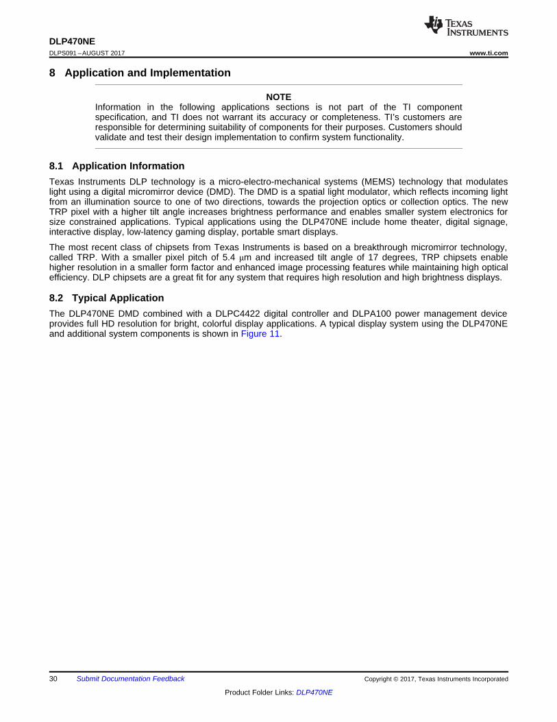
8.2 Typical ApplicationThe DLP470NE DMD combined with a DLPC4422 digital controller and DLPA100 power management deviceprovides full HD resolution for bright, colorful display applications. A typical display system using the DLP470NEand additional system components is shown in Figure 11.
DLPC4422Master ASIC
DLPA100(ASIC Voltages)
Con
nect
or
JTAG
Flash
Input from Front End
Board: 1920 × 1200
I2C
23 16DATAADDR
2 × LVDS (1920 × 1200)
DAD control and SCP control
FE control
1.1 V
1.8 V
2.5 V
3.3 V
5 V
Colorwheel motor control
Illumination Control (LED, laser, and lamp control)
12 V
Control signals
GPIO lines
DATA, 30-bit, 1920 × 1200
Field, H/ V-Sync, DE, CLK
DATA(TTL)
Peripherals
USB 1.0, IR, I2C, SPI
Con
nect
or DLP470NEDMDLevel
Translators
TMP411 Temperature
Sensor
TPS65145(DMD Voltages)
3.3 V 10 V
±14 V
18 V
To DMD
Copyright © 2017, Texas Instruments Incorporated
DLP470NEwww.ti.com DLPS091 –AUGUST 2017
31
Product Folder Links: DLP470NE
Submit Documentation FeedbackCopyright © 2017, Texas Instruments Incorporated
Figure 11. Typical 1080P Application Diagram
32
DLP470NEDLPS091 –AUGUST 2017 www.ti.com
Product Folder Links: DLP470NE
Submit Documentation Feedback Copyright © 2017, Texas Instruments Incorporated
8.2.1 Design RequirementsA DLP470NE projection system is created by using the DMD chipset, including the DLP470NE, DLPC4422, andDLPA100. The DLP470NE is used as the core imaging device in the display system and contains a 0.47-incharray of micromirrors. The DLPC4422 controller is the digital interface between the DMD and the rest of thesystem, taking digital input from front end receiver and driving the DMD over a high speed interface. TheDLPA100 power management device provides voltage regulators for the DMD, controller, and illuminationfunctionality.
Other core components of the display system include an illumination source, an optical engine for the illuminationand projection optics, other electrical and mechanical components, and software. The illumination source optionsinclude lamp, LED, laser or laser phosphor. The type of illumination used and desired brightness will have amajor effect on the overall system design and size.
8.2.2 Detailed Design ProcedureFor connecting the DLPC4422 display controller and the DLP470NE DMD, see the reference design schematic.For a complete the DLP system, an optical module or light engine is required that contains the DLP470NE DMD,associated illumination sources, optical elements, and necessary mechanical components.
To ensure reliable operation, the DLP470NE DMD must always be used with the DLPC4422 display controllersand a DLPA100 PMIC driver. Refer to PCB Design Requirements for DLP Standard TRP Digital MicromirrorDevices for the DMD board design and manufacturing handling of the DMD sub assemblies.
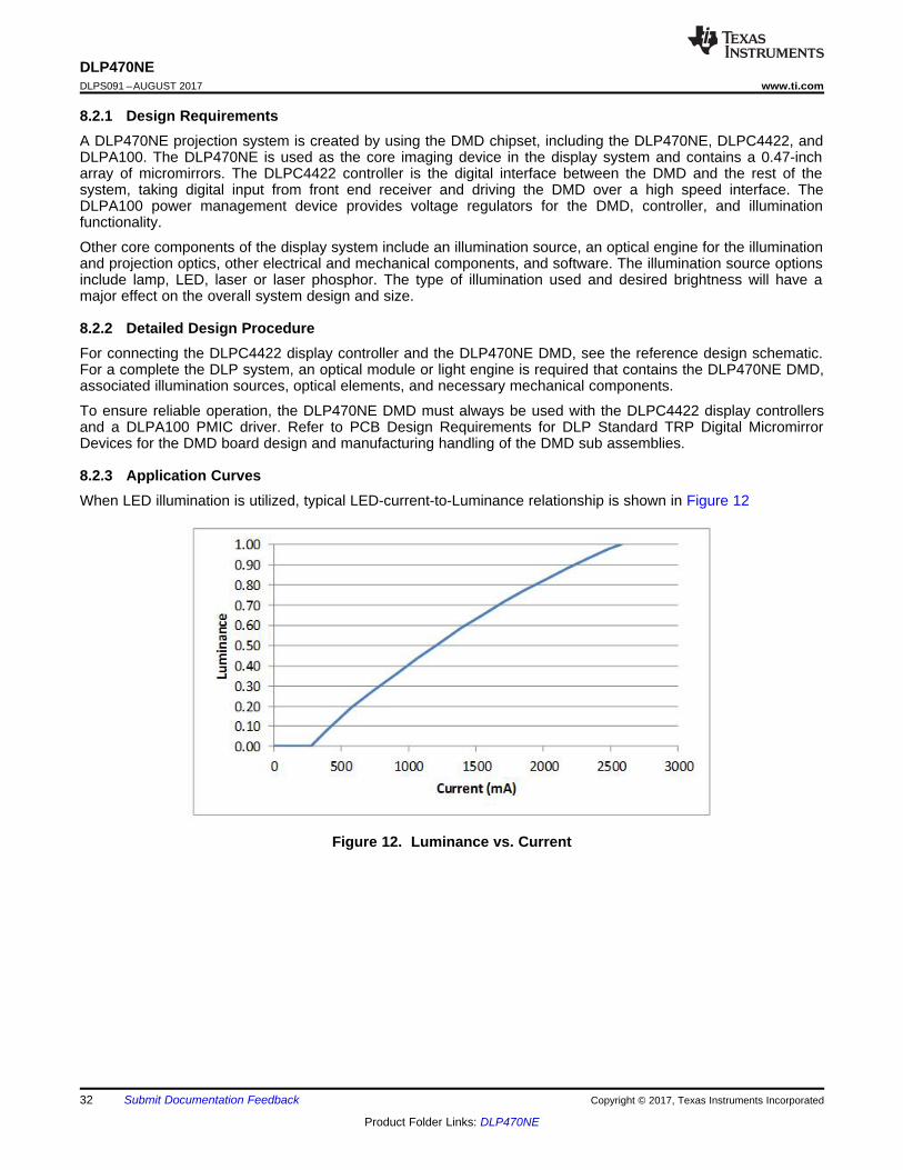
8.2.3 Application CurvesWhen LED illumination is utilized, typical LED-current-to-Luminance relationship is shown in Figure 12
Figure 12. Luminance vs. Current

33
DLP470NEwww.ti.com DLPS091 –AUGUST 2017
Product Folder Links: DLP470NE
Submit Documentation FeedbackCopyright © 2017, Texas Instruments Incorporated
9 Power Supply RecommendationsThe following power supplies are all required to operate the DMD:• VSS• VBIAS• VCC• VOFFSET• VRESET
DMD power-up and power-down sequencing is strictly controlled by the DLP display controller.
CAUTIONFor reliable operation of the DMD, the following power supply sequencingrequirements must be followed. Failure to adhere to any of the prescribed power-upand power-down requirements may affect device reliability. See Figure 13 DMD PowerSupply Sequencing Requirements.
VBIAS, VCC, VOFFSET, and VRESET power supplies must be coordinated duringpower-up and power-down operations. Failure to meet any of the below requirementswill result in a significant reduction in the DMD reliability and lifetime. Common groundVSS must also be connected.
9.1 DMD Power Supply Power-Up Procedure• During power-up, VCC must always start and settle before VOFFSET plus Delay1 specified in Table 8,
VBIAS, and VRESET voltages are applied to the DMD.• During power-up, it is a strict requirement that the voltage difference between VBIAS and VOFFSET must be
within the specified limit shown in Recommended Operating Conditions.• During power-up, there is no requirement for the relative timing of VRESET with respect to VBIAS.• Power supply slew rates during power-up are flexible, provided that the transient voltage levels follow the
requirements specified in Absolute Maximum Ratings, in Recommended Operating Conditions, and inFigure 13.
• During power-up, LVCMOS input pins must not be driven high until after VCC have settled at operatingvoltages listed in Recommended Operating Conditions.
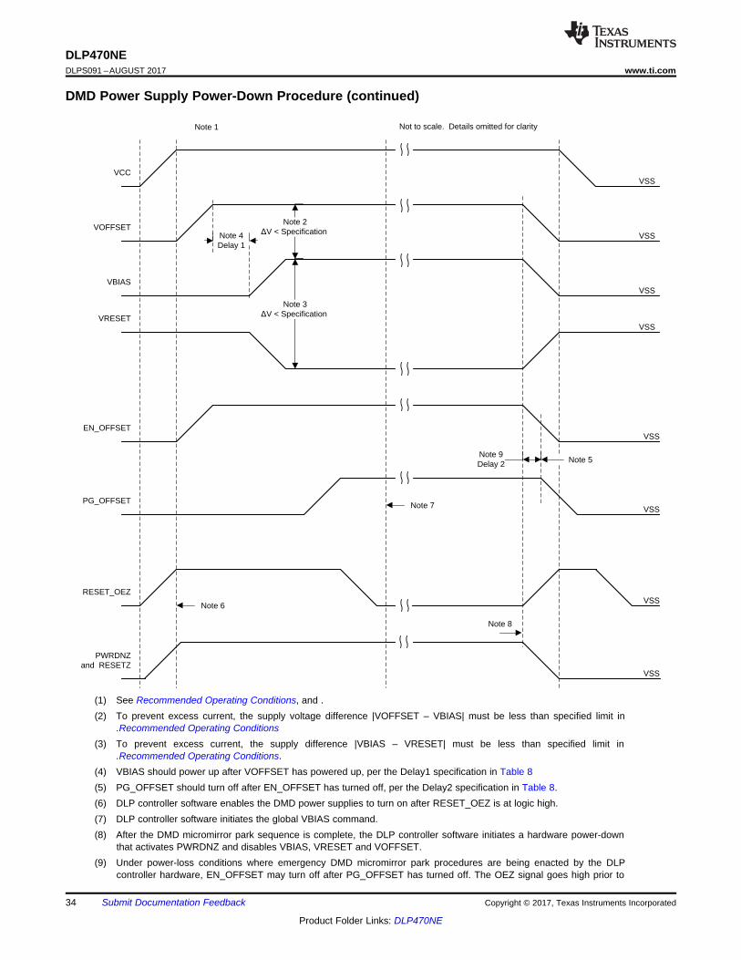
9.2 DMD Power Supply Power-Down Procedure• During power-down, VCC must be supplied until after VBIAS, VRESET, and VOFFSET are discharged to
within the specified limit of ground. See Table 8.• During power-down, it is a strict requirement that the voltage difference between VBIAS and VOFFSET must
be within the specified limit shown in Recommended Operating Conditions.• During power-down, there is no requirement for the relative timing of VRESET with respect to VBIAS.• Power supply slew rates during power-down are flexible, provided that the transient voltage levels follow the
requirements specified in Absolute Maximum Ratings, in Recommended Operating Conditions, and inFigure 13.
• During power-down, LVCMOS input pins must be less than specified in Recommended Operating Conditions.
VCC
VOFFSET
VRESET
RESET_OEZ
PG_OFFSET
EN_OFFSET
PWRDNZ and RESETZ
VBIAS
Note 5
Note 8
Note 7
Note 6
Not to scale. Details omitted for clarity Note 1
Note 4Delay 1
Note 2ûV < Specification
Note 3ûV < Specification
Note 9Delay 2
VSS
VSS
VSS
VSS
VSS
VSS
VSS
VSS
34
DLP470NEDLPS091 –AUGUST 2017 www.ti.com
Product Folder Links: DLP470NE
Submit Documentation Feedback Copyright © 2017, Texas Instruments Incorporated
DMD Power Supply Power-Down Procedure (continued)
(1) See Recommended Operating Conditions, and .(2) To prevent excess current, the supply voltage difference |VOFFSET – VBIAS| must be less than specified limit in
.Recommended Operating Conditions(3) To prevent excess current, the supply difference |VBIAS – VRESET| must be less than specified limit in
.Recommended Operating Conditions.(4) VBIAS should power up after VOFFSET has powered up, per the Delay1 specification in Table 8(5) PG_OFFSET should turn off after EN_OFFSET has turned off, per the Delay2 specification in Table 8.(6) DLP controller software enables the DMD power supplies to turn on after RESET_OEZ is at logic high.(7) DLP controller software initiates the global VBIAS command.(8) After the DMD micromirror park sequence is complete, the DLP controller software initiates a hardware power-down
that activates PWRDNZ and disables VBIAS, VRESET and VOFFSET.(9) Under power-loss conditions where emergency DMD micromirror park procedures are being enacted by the DLP
controller hardware, EN_OFFSET may turn off after PG_OFFSET has turned off. The OEZ signal goes high prior to
35
DLP470NEwww.ti.com DLPS091 –AUGUST 2017
Product Folder Links: DLP470NE
Submit Documentation FeedbackCopyright © 2017, Texas Instruments Incorporated
DMD Power Supply Power-Down Procedure (continued)PG_OFFSET turning off to indicate the DMD micromirror has completed the emergency park procedures.
Figure 13. DMD Power Supply Requirements
Table 8. DMD Power-Supply RequirementsPARAMETER DESCRIPTION MIN NOM MAX UNIT
Delay1 Delay from VOFFSET settled at recommended operating voltage toVBIAS and VRESET power up 1 2 ms
Delay2 PG_OFFSET hold time after EN_OFFSET goes low 100 ns
36
DLP470NEDLPS091 –AUGUST 2017 www.ti.com
Product Folder Links: DLP470NE
Submit Documentation Feedback Copyright © 2017, Texas Instruments Incorporated
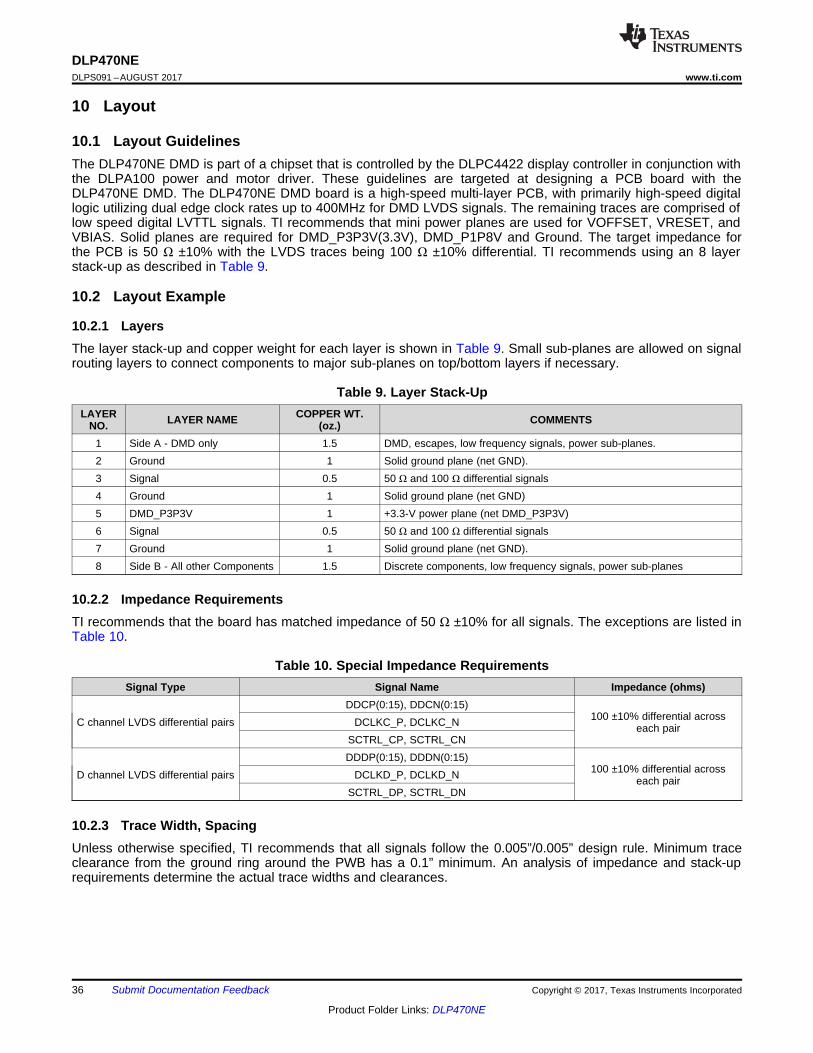
10 Layout
10.1 Layout GuidelinesThe DLP470NE DMD is part of a chipset that is controlled by the DLPC4422 display controller in conjunction withthe DLPA100 power and motor driver. These guidelines are targeted at designing a PCB board with theDLP470NE DMD. The DLP470NE DMD board is a high-speed multi-layer PCB, with primarily high-speed digitallogic utilizing dual edge clock rates up to 400MHz for DMD LVDS signals. The remaining traces are comprised oflow speed digital LVTTL signals. TI recommends that mini power planes are used for VOFFSET, VRESET, andVBIAS. Solid planes are required for DMD_P3P3V(3.3V), DMD_P1P8V and Ground. The target impedance forthe PCB is 50 Ω ±10% with the LVDS traces being 100 Ω ±10% differential. TI recommends using an 8 layerstack-up as described in Table 9.
10.2 Layout Example
10.2.1 LayersThe layer stack-up and copper weight for each layer is shown in Table 9. Small sub-planes are allowed on signalrouting layers to connect components to major sub-planes on top/bottom layers if necessary.
Table 9. Layer Stack-UpLAYER
NO. LAYER NAME COPPER WT.(oz.) COMMENTS
1 Side A - DMD only 1.5 DMD, escapes, low frequency signals, power sub-planes.2 Ground 1 Solid ground plane (net GND).3 Signal 0.5 50 Ω and 100 Ω differential signals4 Ground 1 Solid ground plane (net GND)5 DMD_P3P3V 1 +3.3-V power plane (net DMD_P3P3V)6 Signal 0.5 50 Ω and 100 Ω differential signals7 Ground 1 Solid ground plane (net GND).8 Side B - All other Components 1.5 Discrete components, low frequency signals, power sub-planes
10.2.2 Impedance RequirementsTI recommends that the board has matched impedance of 50 Ω ±10% for all signals. The exceptions are listed inTable 10.
Table 10. Special Impedance RequirementsSignal Type Signal Name Impedance (ohms)
C channel LVDS differential pairsDDCP(0:15), DDCN(0:15)
100 ±10% differential acrosseach pairDCLKC_P, DCLKC_N
SCTRL_CP, SCTRL_CN
D channel LVDS differential pairsDDDP(0:15), DDDN(0:15)
100 ±10% differential acrosseach pairDCLKD_P, DCLKD_N
SCTRL_DP, SCTRL_DN
10.2.3 Trace Width, SpacingUnless otherwise specified, TI recommends that all signals follow the 0.005”/0.005” design rule. Minimum traceclearance from the ground ring around the PWB has a 0.1” minimum. An analysis of impedance and stack-uprequirements determine the actual trace widths and clearances.

37
DLP470NEwww.ti.com DLPS091 –AUGUST 2017
Product Folder Links: DLP470NE
Submit Documentation FeedbackCopyright © 2017, Texas Instruments Incorporated
10.2.3.1 Voltage Signals
Table 11. Special Trace Widths, Spacing Requirements
SIGNAL NAME MINIMUM TRACE WIDTH TOPINS (MIL) LAYOUT REQUIREMENT
GND 15 Maximize trace width to connecting pinDMD_P3P3V 15 Maximize trace width to connecting pinDMD_P1P8V 15 Maximize trace width to connecting pinVOFFSET 15 Create mini plane from U2 to U3VRESET 15 Create mini plane from U2 to U3VBIAS 15 Create mini plane from U2 to U3All U3 controlconnections 10 Use 10 mil etch to connect all signals/voltages to DMD pads

TI internal numbering2-Dimension matrix code
(device number and serial number)
YYYYYYY*1910-5bbcB
DMD part number
GHXXXXX LLLLLLM
Part 2 of serial number (7 characters)
Part 1 of serial number (7 characters)
Package Type
FXHDLP470NE
Device Descriptor
38
DLP470NEDLPS091 –AUGUST 2017 www.ti.com
Product Folder Links: DLP470NE
Submit Documentation Feedback Copyright © 2017, Texas Instruments Incorporated
11 Device and Documentation Support
11.1 Device Support
11.1.1 Device Nomenclature
Figure 14. Part Number Description
11.1.2 Device MarkingsThe device marking includes both human-readable information and a 2-dimensional matrix code. The human-readable information is described in Figure 15. The 2-dimensional matrix code is an alpha-numeric characterstring that contains the DMD part number, part 1 of serial number, and part 2 of serial number. The firstcharacter of the DMD Serial Number (part 1) is the manufacturing year. The second character of the DMD SerialNumber (part 1) is the manufacturing month. The last character of the DMD Serial Number (part 2) is the biasvoltage bin letter.
Example: *1910-503AB GHXXXXX LLLLLLM
Figure 15. DMD Marking Locations
11.2 Documentation Support
11.2.1 Related DocumentationThe following documents contain additional information related to the chipset components used with theDLP470NE.• DLPC4422 Display Controller Data Sheet• DLPA100 Power and Motor Driver Data Sheet
39
DLP470NEwww.ti.com DLPS091 –AUGUST 2017
Product Folder Links: DLP470NE
Submit Documentation FeedbackCopyright © 2017, Texas Instruments Incorporated
11.3 Receiving Notification of Documentation UpdatesTo receive notification of documentation updates, navigate to the device product folder on ti.com. In the upperright corner, click on Alert me to register and receive a weekly digest of any product information that haschanged. For change details, review the revision history included in any revised document.
11.4 Community ResourcesThe following links connect to TI community resources. Linked contents are provided "AS IS" by the respectivecontributors. They do not constitute TI specifications and do not necessarily reflect TI's views; see TI's Terms ofUse.
TI E2E™ Online Community TI's Engineer-to-Engineer (E2E) Community. Created to foster collaborationamong engineers. At e2e.ti.com, you can ask questions, share knowledge, explore ideas and helpsolve problems with fellow engineers.
Design Support TI's Design Support Quickly find helpful E2E forums along with design support tools andcontact information for technical support.
11.5 TrademarksE2E is a trademark of Texas Instruments.DLP is a registered trademark of Texas Instruments.All other trademarks are the property of their respective owners.
11.6 Electrostatic Discharge CautionThese devices have limited built-in ESD protection. The leads should be shorted together or the device placed in conductive foamduring storage or handling to prevent electrostatic damage to the MOS gates.
11.7 GlossarySLYZ022 — TI Glossary.
This glossary lists and explains terms, acronyms, and definitions.
40
DLP470NEDLPS091 –AUGUST 2017 www.ti.com
Product Folder Links: DLP470NE
Submit Documentation Feedback Copyright © 2017, Texas Instruments Incorporated
12 Mechanical, Packaging, and Orderable InformationThe following pages include mechanical, packaging, and orderable information. This information is the mostcurrent data available for the designated devices. This data is subject to change without notice and revision ofthis document. For browser-based versions of this data sheet, refer to the left-hand navigation.

PACKAGE OPTION ADDENDUM
www.ti.com 31-Jul-2018
Addendum-Page 1
PACKAGING INFORMATION
Orderable Device Status(1)
Package Type PackageDrawing
Pins PackageQty
Eco Plan(2)
Lead/Ball Finish(6)
MSL Peak Temp(3)
Op Temp (°C) Device Marking(4/5)
Samples
DLP470NEFXH ACTIVE CLGA FXH 257 33 RoHS & Green(In Work)
Call TI Level-1-NC-NC
(1) The marketing status values are defined as follows:ACTIVE: Product device recommended for new designs.LIFEBUY: TI has announced that the device will be discontinued, and a lifetime-buy period is in effect.NRND: Not recommended for new designs. Device is in production to support existing customers, but TI does not recommend using this part in a new design.PREVIEW: Device has been announced but is not in production. Samples may or may not be available.OBSOLETE: TI has discontinued the production of the device.
(2) RoHS: TI defines "RoHS" to mean semiconductor products that are compliant with the current EU RoHS requirements for all 10 RoHS substances, including the requirement that RoHS substancedo not exceed 0.1% by weight in homogeneous materials. Where designed to be soldered at high temperatures, "RoHS" products are suitable for use in specified lead-free processes. TI mayreference these types of products as "Pb-Free".RoHS Exempt: TI defines "RoHS Exempt" to mean products that contain lead but are compliant with EU RoHS pursuant to a specific EU RoHS exemption.Green: TI defines "Green" to mean the content of Chlorine (Cl) and Bromine (Br) based flame retardants meet JS709B low halogen requirements of <=1000ppm threshold. Antimony trioxide basedflame retardants must also meet the <=1000ppm threshold requirement.
(3) MSL, Peak Temp. - The Moisture Sensitivity Level rating according to the JEDEC industry standard classifications, and peak solder temperature.
(4) There may be additional marking, which relates to the logo, the lot trace code information, or the environmental category on the device.
(5) Multiple Device Markings will be inside parentheses. Only one Device Marking contained in parentheses and separated by a "~" will appear on a device. If a line is indented then it is a continuationof the previous line and the two combined represent the entire Device Marking for that device.
(6) Lead/Ball Finish - Orderable Devices may have multiple material finish options. Finish options are separated by a vertical ruled line. Lead/Ball Finish values may wrap to two lines if the finishvalue exceeds the maximum column width.
Important Information and Disclaimer:The information provided on this page represents TI's knowledge and belief as of the date that it is provided. TI bases its knowledge and belief on informationprovided by third parties, and makes no representation or warranty as to the accuracy of such information. Efforts are underway to better integrate information from third parties. TI has taken andcontinues to take reasonable steps to provide representative and accurate information but may not have conducted destructive testing or chemical analysis on incoming materials and chemicals.TI and TI suppliers consider certain information to be proprietary, and thus CAS numbers and other limited information may not be available for release.
In no event shall TI's liability arising out of such information exceed the total purchase price of the TI part(s) at issue in this document sold by TI to Customer on an annual basis.


IMPORTANT NOTICE
Texas Instruments Incorporated (TI) reserves the right to make corrections, enhancements, improvements and other changes to itssemiconductor products and services per JESD46, latest issue, and to discontinue any product or service per JESD48, latest issue. Buyersshould obtain the latest relevant information before placing orders and should verify that such information is current and complete.TI’s published terms of sale for semiconductor products (http://www.ti.com/sc/docs/stdterms.htm) apply to the sale of packaged integratedcircuit products that TI has qualified and released to market. Additional terms may apply to the use or sale of other types of TI products andservices.Reproduction of significant portions of TI information in TI data sheets is permissible only if reproduction is without alteration and isaccompanied by all associated warranties, conditions, limitations, and notices. TI is not responsible or liable for such reproduceddocumentation. Information of third parties may be subject to additional restrictions. Resale of TI products or services with statementsdifferent from or beyond the parameters stated by TI for that product or service voids all express and any implied warranties for theassociated TI product or service and is an unfair and deceptive business practice. TI is not responsible or liable for any such statements.Buyers and others who are developing systems that incorporate TI products (collectively, “Designers”) understand and agree that Designersremain responsible for using their independent analysis, evaluation and judgment in designing their applications and that Designers havefull and exclusive responsibility to assure the safety of Designers' applications and compliance of their applications (and of all TI productsused in or for Designers’ applications) with all applicable regulations, laws and other applicable requirements. Designer represents that, withrespect to their applications, Designer has all the necessary expertise to create and implement safeguards that (1) anticipate dangerousconsequences of failures, (2) monitor failures and their consequences, and (3) lessen the likelihood of failures that might cause harm andtake appropriate actions. Designer agrees that prior to using or distributing any applications that include TI products, Designer willthoroughly test such applications and the functionality of such TI products as used in such applications.TI’s provision of technical, application or other design advice, quality characterization, reliability data or other services or information,including, but not limited to, reference designs and materials relating to evaluation modules, (collectively, “TI Resources”) are intended toassist designers who are developing applications that incorporate TI products; by downloading, accessing or using TI Resources in anyway, Designer (individually or, if Designer is acting on behalf of a company, Designer’s company) agrees to use any particular TI Resourcesolely for this purpose and subject to the terms of this Notice.TI’s provision of TI Resources does not expand or otherwise alter TI’s applicable published warranties or warranty disclaimers for TIproducts, and no additional obligations or liabilities arise from TI providing such TI Resources. TI reserves the right to make corrections,enhancements, improvements and other changes to its TI Resources. TI has not conducted any testing other than that specificallydescribed in the published documentation for a particular TI Resource.Designer is authorized to use, copy and modify any individual TI Resource only in connection with the development of applications thatinclude the TI product(s) identified in such TI Resource. NO OTHER LICENSE, EXPRESS OR IMPLIED, BY ESTOPPEL OR OTHERWISETO ANY OTHER TI INTELLECTUAL PROPERTY RIGHT, AND NO LICENSE TO ANY TECHNOLOGY OR INTELLECTUAL PROPERTYRIGHT OF TI OR ANY THIRD PARTY IS GRANTED HEREIN, including but not limited to any patent right, copyright, mask work right, orother intellectual property right relating to any combination, machine, or process in which TI products or services are used. Informationregarding or referencing third-party products or services does not constitute a license to use such products or services, or a warranty orendorsement thereof. Use of TI Resources may require a license from a third party under the patents or other intellectual property of thethird party, or a license from TI under the patents or other intellectual property of TI.TI RESOURCES ARE PROVIDED “AS IS” AND WITH ALL FAULTS. TI DISCLAIMS ALL OTHER WARRANTIES ORREPRESENTATIONS, EXPRESS OR IMPLIED, REGARDING RESOURCES OR USE THEREOF, INCLUDING BUT NOT LIMITED TOACCURACY OR COMPLETENESS, TITLE, ANY EPIDEMIC FAILURE WARRANTY AND ANY IMPLIED WARRANTIES OFMERCHANTABILITY, FITNESS FOR A PARTICULAR PURPOSE, AND NON-INFRINGEMENT OF ANY THIRD PARTY INTELLECTUALPROPERTY RIGHTS. TI SHALL NOT BE LIABLE FOR AND SHALL NOT DEFEND OR INDEMNIFY DESIGNER AGAINST ANY CLAIM,INCLUDING BUT NOT LIMITED TO ANY INFRINGEMENT CLAIM THAT RELATES TO OR IS BASED ON ANY COMBINATION OFPRODUCTS EVEN IF DESCRIBED IN TI RESOURCES OR OTHERWISE. IN NO EVENT SHALL TI BE LIABLE FOR ANY ACTUAL,DIRECT, SPECIAL, COLLATERAL, INDIRECT, PUNITIVE, INCIDENTAL, CONSEQUENTIAL OR EXEMPLARY DAMAGES INCONNECTION WITH OR ARISING OUT OF TI RESOURCES OR USE THEREOF, AND REGARDLESS OF WHETHER TI HAS BEENADVISED OF THE POSSIBILITY OF SUCH DAMAGES.Unless TI has explicitly designated an individual product as meeting the requirements of a particular industry standard (e.g., ISO/TS 16949and ISO 26262), TI is not responsible for any failure to meet such industry standard requirements.Where TI specifically promotes products as facilitating functional safety or as compliant with industry functional safety standards, suchproducts are intended to help enable customers to design and create their own applications that meet applicable functional safety standardsand requirements. Using products in an application does not by itself establish any safety features in the application. Designers mustensure compliance with safety-related requirements and standards applicable to their applications. Designer may not use any TI products inlife-critical medical equipment unless authorized officers of the parties have executed a special contract specifically governing such use.Life-critical medical equipment is medical equipment where failure of such equipment would cause serious bodily injury or death (e.g., lifesupport, pacemakers, defibrillators, heart pumps, neurostimulators, and implantables). Such equipment includes, without limitation, allmedical devices identified by the U.S. Food and Drug Administration as Class III devices and equivalent classifications outside the U.S.TI may expressly designate certain products as completing a particular qualification (e.g., Q100, Military Grade, or Enhanced Product).Designers agree that it has the necessary expertise to select the product with the appropriate qualification designation for their applicationsand that proper product selection is at Designers’ own risk. Designers are solely responsible for compliance with all legal and regulatoryrequirements in connection with such selection.Designer will fully indemnify TI and its representatives against any damages, costs, losses, and/or liabilities arising out of Designer’s non-compliance with the terms and provisions of this Notice.
Mailing Address: Texas Instruments, Post Office Box 655303, Dallas, Texas 75265Copyright © 2018, Texas Instruments Incorporated