Embed Size (px)
Citation preview
SCALE™-2+ 2SC0106T
www.power.com/igbt-driver Page 1
SCALE™-2+ 2SC0106T
Preliminary Description & Application Manual
Dual-channel ultra-compact SCALE™-2+ driver core
Abstract
The new SCALE™-2+ dual-driver core 2SC0106T combines unrivalled compactness with broad applicability.
The driver was designed for universal applications requiring high reliability. The 2SC0106T drives all usual IGBT modules up to 450A/1200V or 600A/650V.
The 2SC0106T is the most compact driver core available for industrial applications, with a footprint of only 45.5mm x 31mm and an insertion height of 13mm. It allows even the most restricted insertion spaces to be
efficiently used.
Fig. 1 2SC0106T driver core
SCALE™-2+ 2SC0106T Preliminary Description & Application Manual
www.power.com/igbt-driver Page 2
Contents
Driver Overview ............................................................................................................................. 3
Pin Designation .............................................................................................................................. 6
Recommended Interface Circuitry for the Primary-Side Connector .............................................. 6
Description of Primary-Side Interface ........................................................................................... 7
General ............................................................................................................................... 7
VCC terminal ....................................................................................................................... 7
INA, INB (channel drive inputs, e.g. PWM) ............................................................................. 7
SO (status output) ............................................................................................................... 7
TB (input for adjusting the blocking time Tb) .......................................................................... 8
Recommended Interface Circuitry for the Secondary-Side Connectors ........................................ 9
Description of Secondary-Side Interfaces ..................................................................................... 9
General ............................................................................................................................... 9
DC/DC output (VISOx) and emitter (VEx) terminals .............................................................. 10
Collector sense (VCEx) with resistors ................................................................................... 10
Desaturation protection with sense diodes ........................................................................... 12
Disabling the VCE,sat detection .............................................................................................. 14
Gate terminal (Gx) ............................................................................................................. 14
Gate clamping and STO (Safe Torque Off) ........................................................................... 14
Soft Shut Down (SSD) function ........................................................................................... 15
How Do 2SC0106T SCALE-2+ Drivers Work in Detail? ................................................................ 15
Power supply and electrical isolation ................................................................................... 15
Power-supply monitoring .................................................................................................... 16
Additional application support for 2SC0106T ........................................................................ 16
Electrical Ratings for UL recognized types .................................................................................. 16
Bibliography ................................................................................................................................. 16
The Information Source: SCALE-2+ Driver Data Sheets ............................................................. 17
Quite Special: Customized SCALE-2+ Drivers .............................................................................. 17
Technical Support ........................................................................................................................ 17
Quality .......................................................................................................................................... 17
Legal Disclaimer ........................................................................................................................... 17
Ordering Information ................................................................................................................... 18
Information about Other Products .............................................................................................. 18
Power Integrations Sales Offices ................................................................................................. 19
SCALE™-2+ 2SC0106T Preliminary Description & Application Manual
www.power.com/igbt-driver Page 3
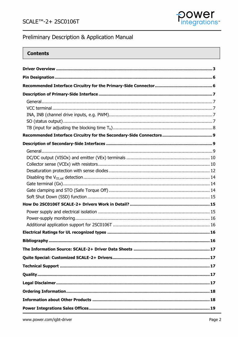
Driver Overview
The 2SC0106T is a driver core equipped with Power Integrations' latest SCALE-2+ chipset. The SCALE-2+ chipset consists of two application-specific integrated circuits (ASICs) that cover the main range of functions
needed to design intelligent gate drivers. The driver core targets applications using 600V-1200V IGBTs such as general purpose drives, UPS, solar converters and medical applications. The driver supports switching
frequencies up to 50kHz. It comprises all functionality for an advanced dual-channel IGBT gate driver including
an isolated DC/DC converter, short-circuit protection, Soft Shut Down (SSD) and supply-voltage monitoring.
Fig. 2 Block diagram of driver core 2SC0106T
SCALE™-2+ 2SC0106T Preliminary Description & Application Manual
www.power.com/igbt-driver Page 4
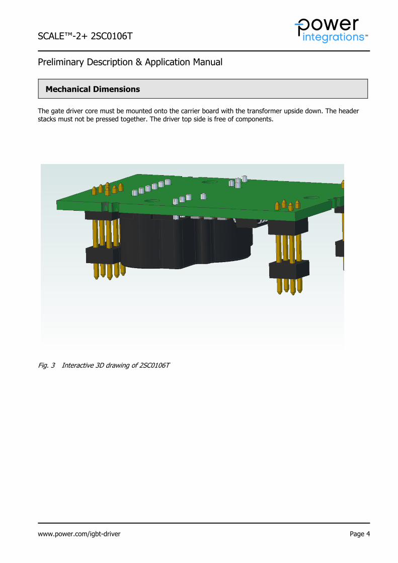
Mechanical Dimensions
The gate driver core must be mounted onto the carrier board with the transformer upside down. The header
stacks must not be pressed together. The driver top side is free of components.
Fig. 3 Interactive 3D drawing of 2SC0106T
SCALE™-2+ 2SC0106T Preliminary Description & Application Manual
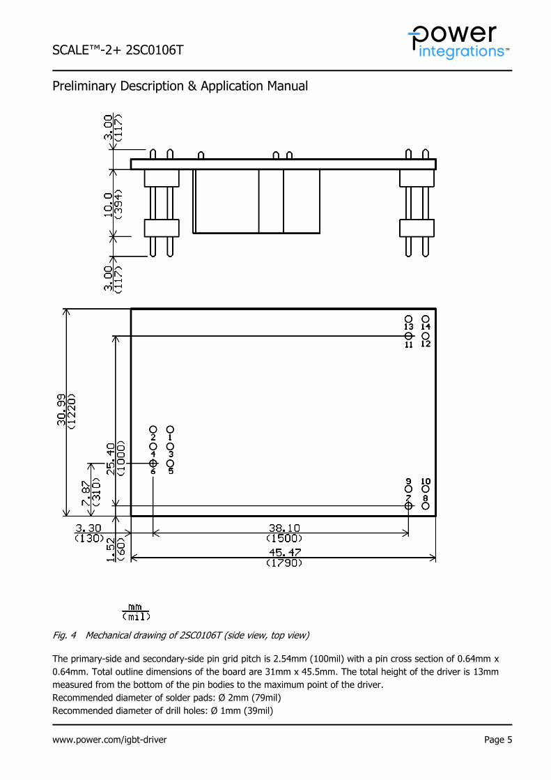
www.power.com/igbt-driver Page 5
Fig. 4 Mechanical drawing of 2SC0106T (side view, top view)
The primary-side and secondary-side pin grid pitch is 2.54mm (100mil) with a pin cross section of 0.64mm x
0.64mm. Total outline dimensions of the board are 31mm x 45.5mm. The total height of the driver is 13mm
measured from the bottom of the pin bodies to the maximum point of the driver.
Recommended diameter of solder pads: Ø 2mm (79mil)
Recommended diameter of drill holes: Ø 1mm (39mil)
SCALE™-2+ 2SC0106T Preliminary Description & Application Manual
www.power.com/igbt-driver Page 6
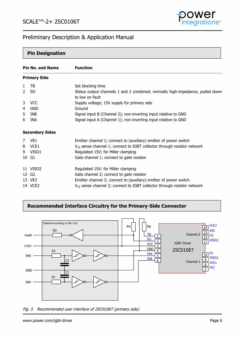
Pin Designation
Pin No. and Name Function
Primary Side
1 TB Set blocking time
2 SO Status output channels 1 and 2 combined; normally high-impedance, pulled down
to low on fault
3 VCC Supply voltage; 15V supply for primary side
4 GND Ground
5 INB Signal input B (Channel 2); non-inverting input relative to GND
6 INA Signal input A (Channel 1); non-inverting input relative to GND
Secondary Sides
7 VE1 Emitter channel 1; connect to (auxiliary) emitter of power switch
8
9
VCE1
VISO1
VCE sense channel 1; connect to IGBT collector through resistor network
Regulated 15V; for Miller clamping
10 G1 Gate channel 1; connect to gate resistor
11 VISO2 Regulated 15V; for Miller clamping
12
13
G2
VE2
Gate channel 2; connect to gate resistor
Emitter channel 2; connect to (auxiliary) emitter of power switch
14 VCE2 VCE sense channel 2; connect to IGBT collector through resistor network
Recommended Interface Circuitry for the Primary-Side Connector
Fig. 5 Recommended user interface of 2SC0106T (primary side)
SCALE™-2+ 2SC0106T Preliminary Description & Application Manual
www.power.com/igbt-driver Page 7
Note: 2SC0106T is an ultra-fast gate driver core. Any input noise on INA and INB with an amplitude of more than 2.6V will be transferred to a secondary-side gate switching signal. This can overload the DC-DC
converter and damage the driver. The corresponding IGBTs or MOSFETs can also be damaged. Appropriate protection circuits are recommended according to the specific setup. Application note
AN-1101 /1/ proposes corresponding protection circuits.
Description of Primary-Side Interface
General
The primary-side interface of the driver 2SC0106T is very simple and easy to use. The primary side is fully insulated from both secondary (high-voltage) sides. The driver channels work independently of each other.
The driver primary side is equipped with a 6-pin interface connector with the following terminals:
1 x power-supply terminal
2 x drive signal inputs
1 x status output (fault return)
1 x input to set the blocking time
1x ground terminal GND
All inputs and outputs are ESD-protected. Moreover, all digital inputs have Schmitt-trigger characteristics.
VCC terminal
The driver has one VCC terminal on the interface connector. It supplies the primary-side electronics as well as
the DC-DC converter to supply the secondary sides with 15V.
The driver limits the inrush current at startup and no external current limitation of the voltage source for VCC is needed for this purpose.
INA, INB (channel drive inputs, e.g. PWM)
INA and INB are drive inputs. They safely recognize signals in the whole logic-level range between 3.3V and 15V. Both input terminals feature Schmitt-trigger characteristics. An input transition is triggered at any edge of
an incoming signal at INA or INB.
SO (status output)
The output SO has an open-drain transistor. When no fault condition is detected, the output has high impedance. An internal current source of 1mA pulls the SO output to a voltage of about 4V when left open.
When a fault condition (primary-side supply undervoltage, secondary-side supply undervoltage, IGBT short
circuit) is detected, the status output SO goes to low (connected to GND).
The maximum SO current in a fault condition must not exceed the value specified in the driver data sheet /2/.

SCALE™-2+ 2SC0106T Preliminary Description & Application Manual
www.power.com/igbt-driver Page 8
How the status information is processed
a) A fault on one of the secondary sides (detection of IGBT module short-circuit or supply undervoltage) is immediately transmitted to the SO output. This output is automatically reset (returning to a high
impedance state) after a blocking time Tb has elapsed (refer to “TB (input for adjusting the blocking time Tb)” for timing information).
b) A supply undervoltage on the primary side is indicated immediately to the SO output. This output is automatically reset (returning to a high impedance state) after the undervoltage on the primary side
disappears and the blocking time Tb has elapsed. Note that the blocking time does not run fully
synchronously on both channels. It is therefore possible that the blocking time of one channel has already elapsed (the channel is free) while the other channel has not yet been released (the channel is blocked)
and SO is still in a fault condition. This time mismatch is typically in the range of 5% of the programmed blocking time (e.g. 6ms for a blocking time of 120ms). It is therefore recommended to wait long enough
after a fault reset before applying switching impulses to ensure that both channels have been effectively
released.
TB (input for adjusting the blocking time Tb)
The terminal TB allows the blocking time Tb to be set by connecting a resistor Rb to GND (see Fig. 5). The
following equation calculates the value of Rb connected between pins TB and GND in order to program the desired blocking time Tb (typical value):
51][0.1][ msTkR bb with 20ms<Tb<130ms and 71kΩ<Rb<181kΩ
The blocking time can also be set to a minimum of 9µs (typical) by selecting Rb=0Ω. Terminal TB must not be
left floating.
SCALE™-2+ 2SC0106T Preliminary Description & Application Manual
www.power.com/igbt-driver Page 9
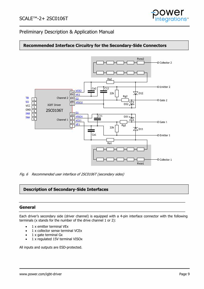
Recommended Interface Circuitry for the Secondary-Side Connectors
Fig. 6 Recommended user interface of 2SC0106T (secondary sides)
Description of Secondary-Side Interfaces
General
Each driver’s secondary side (driver channel) is equipped with a 4-pin interface connector with the following
terminals (x stands for the number of the drive channel 1 or 2):
1 x emitter terminal VEx
1 x collector sense terminal VCEx
1 x gate terminal Gx
1 x regulated 15V terminal VISOx
All inputs and outputs are ESD-protected.
SCALE™-2+ 2SC0106T Preliminary Description & Application Manual
www.power.com/igbt-driver Page 10
DC/DC output (VISOx) and emitter (VEx) terminals
The driver is equipped with blocking capacitors on the secondary side of the DC/DC converter (for values, refer to the data sheet /2/).
Power semiconductors with a gate charge of up to 4μC can be driven without additional capacitors on the secondary side. For IGBTs or MOSFETs with a maximum gate charge of up to 8 µC, a minimum value of 2.5µF
external blocking capacitance is recommended for every 1µC gate charge beyond 4µC. The blocking capacitors
must be placed between VISOx and VEx (C1x in Fig. 6). Their capacitance value must not exceed 10 µF. They must be connected as close as possible to the driver’s terminal pins with minimum inductance. Ceramic
capacitors with a dielectric strength ≥25V are recommended.
Collector sense (VCEx) with resistors
The collector sense of each channel of the 2SC0106T must be connected to the IGBT collector or MOSFET drain with the circuit shown in Fig. 6 or Fig. 7 in order to detect an IGBT or MOSFET short circuit.
During the IGBT off-state, the driver’s internal MOSFET connects pin VCEx to pin COMx. The capacitor Cax is then precharged/discharged to the negative supply voltage, which is about -9V referred to VEx (red circle in
Fig. 7). During this time, a current flows from the collector (blue circle in Fig. 7) via the resistor network and
the diode D1x (BAS416) to VISOx. The current is limited by the resistor chain.
It is recommended to dimension the resistor value of the resistor chain Rvcex in order to obtain a current of
about IRvcex=0.6-1mA flowing through Rvcex (e.g. 800kΩ-1MΩ for VDC-LINK=800V). The current through Rvcex must not exceed 1mA. A high-voltage resistor as well as series-connected resistors may be used. In any case,
the minimum creepage distance required for the application must be considered and the resistor chain must not be allowed to overheat.
The reference voltage is set by an internal resistor Rthx=62kΩ to 9.3V. The driver will therefore safely protect
the IGBT against short-circuit, but not against overcurrent. Overcurrent protection has a lower timing priority and is recommended to be realized within the host controller.

SCALE™-2+ 2SC0106T Preliminary Description & Application Manual
www.power.com/igbt-driver Page 11
Fig. 7 Principe of VCE desaturation protection with resistors
At IGBT turn-on and in the on-state, the driver’s internal MOSFET turns off. While VCE decreases (blue curve in
Fig. 7), Cax is charged from the COMx potential to the IGBT saturation voltage (red curve in Fig. 7). The time required to charge Cax depends on the DC bus voltage, the value of the resistor Rax and the value of the
capacitor Cax. For 1200V IGBTs it is recommended to set Rax=120kΩ. For 600V and 650V IGBTs the
recommended value is Rax=62kΩ.
During the response time, the VCE monitoring circuit is inactive. The response time is the time that elapses
after turn-on of the power semiconductor until the collector voltage is measured. It corresponds to the duration of the short circuit.
The value of the response time capacitors Cax can be determined from the following table in order to set the
desired response time (Rvcex=1MΩ, Rax=120kΩ, DC-link voltage VDC-LINK>500V):
SCALE™-2+ 2SC0106T Preliminary Description & Application Manual
www.power.com/igbt-driver Page 12
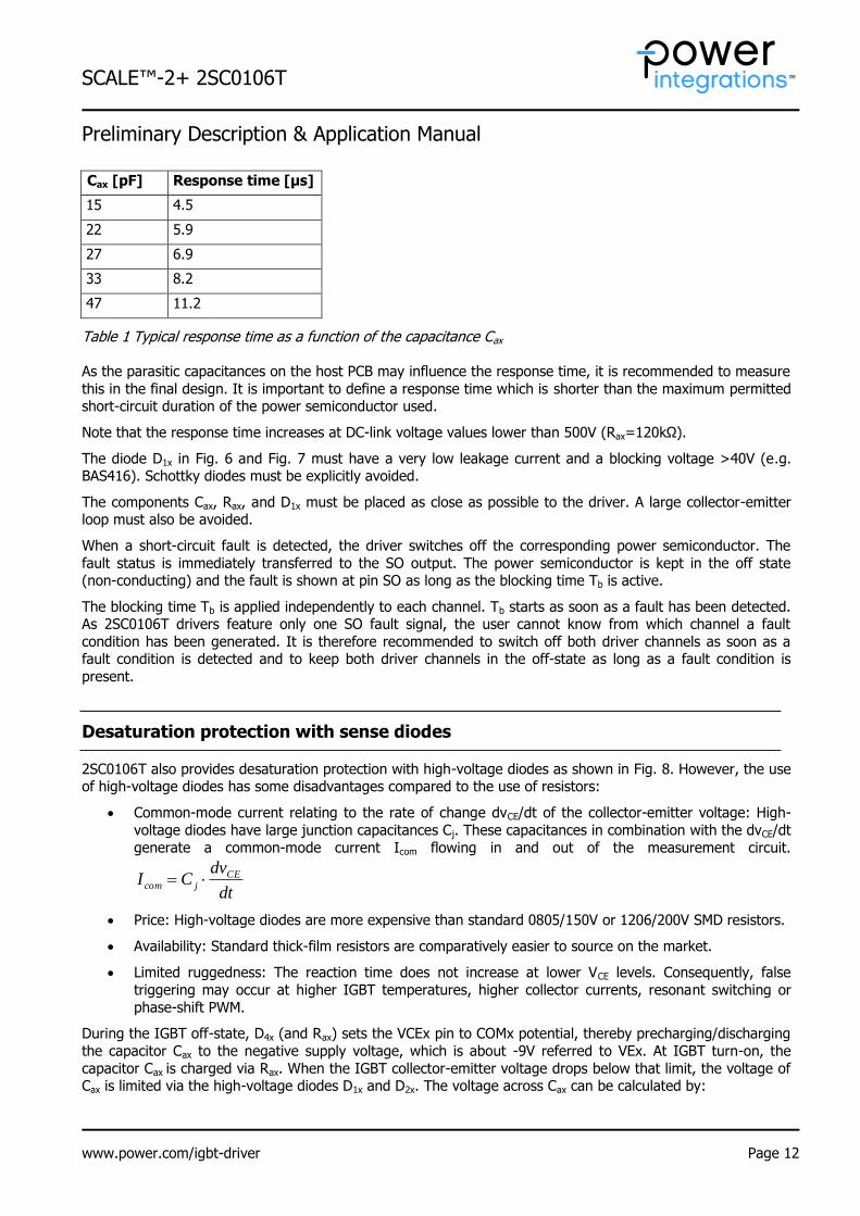
Cax [pF]
Response time [μs]
15 4.5
22 5.9
27 6.9
33 8.2
47 11.2
Table 1 Typical response time as a function of the capacitance Cax
As the parasitic capacitances on the host PCB may influence the response time, it is recommended to measure
this in the final design. It is important to define a response time which is shorter than the maximum permitted short-circuit duration of the power semiconductor used.
Note that the response time increases at DC-link voltage values lower than 500V (Rax=120kΩ).
The diode D1x in Fig. 6 and Fig. 7 must have a very low leakage current and a blocking voltage >40V (e.g. BAS416). Schottky diodes must be explicitly avoided.
The components Cax, Rax, and D1x must be placed as close as possible to the driver. A large collector-emitter loop must also be avoided.
When a short-circuit fault is detected, the driver switches off the corresponding power semiconductor. The
fault status is immediately transferred to the SO output. The power semiconductor is kept in the off state (non-conducting) and the fault is shown at pin SO as long as the blocking time Tb is active.
The blocking time Tb is applied independently to each channel. Tb starts as soon as a fault has been detected. As 2SC0106T drivers feature only one SO fault signal, the user cannot know from which channel a fault
condition has been generated. It is therefore recommended to switch off both driver channels as soon as a fault condition is detected and to keep both driver channels in the off-state as long as a fault condition is
present.
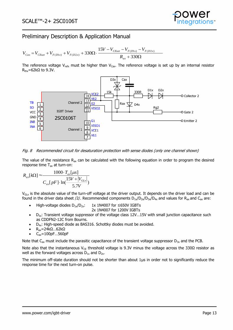
Desaturation protection with sense diodes
2SC0106T also provides desaturation protection with high-voltage diodes as shown in Fig. 8. However, the use of high-voltage diodes has some disadvantages compared to the use of resistors:
Common-mode current relating to the rate of change dvCE/dt of the collector-emitter voltage: High-
voltage diodes have large junction capacitances Cj. These capacitances in combination with the dvCE/dt
generate a common-mode current Icom flowing in and out of the measurement circuit.
dt
dvCI CE
jcom
Price: High-voltage diodes are more expensive than standard 0805/150V or 1206/200V SMD resistors.
Availability: Standard thick-film resistors are comparatively easier to source on the market.
Limited ruggedness: The reaction time does not increase at lower VCE levels. Consequently, false
triggering may occur at higher IGBT temperatures, higher collector currents, resonant switching or
phase-shift PWM.
During the IGBT off-state, D4x (and Rax) sets the VCEx pin to COMx potential, thereby precharging/discharging
the capacitor Cax to the negative supply voltage, which is about -9V referred to VEx. At IGBT turn-on, the
capacitor Cax is charged via Rax. When the IGBT collector-emitter voltage drops below that limit, the voltage of Cax is limited via the high-voltage diodes D1x and D2x. The voltage across Cax can be calculated by:
SCALE™-2+ 2SC0106T Preliminary Description & Application Manual
www.power.com/igbt-driver Page 13
330
15330
)2()1(
)2()1(
ax
xDFxDFCEsat
xDFxDFCEsatCaxR
VVVVVVVV
The reference voltage Vrefx must be higher than VCax. The reference voltage is set up by an internal resistor Rthx=62kΩ to 9.3V.
Fig. 8 Recommended circuit for desaturation protection with sense diodes (only one channel shown)
The value of the resistance Rax can be calculated with the following equation in order to program the desired
response time Tax at turn-on:
)7.5
15ln(][
][1000≈][
V
VVpFC
sTkR
GLx
ax
axax
VGLx is the absolute value of the turn-off voltage at the driver output. It depends on the driver load and can be
found in the driver data sheet /2/. Recommended components D1x/D2x/D3x/D4x and values for Rax and Cax are:
High-voltage diodes D1x/D2x: 1x 1N4007 for ≤650V IGBTs
2x 1N4007 for 1200V IGBTs
D3x: Transient voltage suppressor of the voltage class 12V…15V with small junction capacitance such
as CDDFN2-12C from Bourns.
D4x: High-speed diode as BAS316. Schottky diodes must be avoided.
Rax=24kΩ…62kΩ
Cax=100pF…560pF
Note that Cax must include the parasitic capacitance of the transient voltage suppressor D3x and the PCB.
Note also that the instantaneous VCE threshold voltage is 9.3V minus the voltage across the 330Ω resistor as
well as the forward voltages across D1x and D2x.
The minimum off-state duration should not be shorter than about 1µs in order not to significantly reduce the
response time for the next turn-on pulse.
SCALE™-2+ 2SC0106T Preliminary Description & Application Manual
www.power.com/igbt-driver Page 14
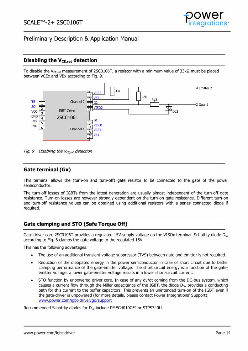
Disabling the VCE,sat detection
To disable the VCE,sat measurement of 2SC0106T, a resistor with a minimum value of 33kΩ must be placed between VCEx and VEx according to Fig. 9.
Fig. 9 Disabling the VCE,sat detection
Gate terminal (Gx)
This terminal allows the (turn-on and turn-off) gate resistor to be connected to the gate of the power
semiconductor.
The turn-off losses of IGBTs from the latest generation are usually almost independent of the turn-off gate resistance. Turn-on losses are however strongly dependent on the turn-on gate resistance. Different turn-on
and turn-off resistance values can be obtained using additional resistors with a series connected diode if required.
Gate clamping and STO (Safe Torque Off)
Gate driver core 2SC0106T provides a regulated 15V supply voltage on the VISOx terminal. Schottky diode D5x
according to Fig. 6 clamps the gate voltage to the regulated 15V.
This has the following advantages:
The use of an additional transient voltage suppressor (TVS) between gate and emitter is not required.
Reduction of the dissipated energy in the power semiconductor in case of short circuit due to better
clamping performance of the gate-emitter voltage. The short circuit energy is a function of the gate-emitter voltage: a lower gate-emitter voltage results in a lower short-circuit current.
STO function by unpowered driver core. In case of any dv/dt coming from the DC-bus system, which
causes a current flow through the Miller capacitance of the IGBT, the diode D5x provides a conducting
path for this current to the buffer capacitors. This prevents an unintended turn-on of the IGBT even if the gate-driver is unpowered (for more details, please contact Power Integrations’ Support):
www.power.com/igbt-driver/go/support
Recommended Schottky diodes for D5x include PMEG4010CEJ or STPS340U.
SCALE™-2+ 2SC0106T Preliminary Description & Application Manual
www.power.com/igbt-driver Page 15
Soft Shut Down (SSD) function
The SSD function reduces the turn-off di/dt to limit the VCE overvoltage as soon as a short-circuit condition is detected. An excessive turn-off overvoltage is therefore avoided and the power semiconductor is turned off
within its safe operating area.
The SSD function is realized with a closed loop scheme which is activated as soon as an IGBT short circuit is
detected. The driver then measures the gate-emitter voltage and adjusts it according to the three following
phases:
In a first step, the gate-emitter voltage is decreased to a defined level controlled with the closed loop
feedback.
The defined level of the gate-emitter voltage is held at the given level to ramp down the collector
current smoothly (e.g. with lower di/dt) until the gate charge profile of the power semiconductor has
reached the end of the Miller plateau. The end of the Miller plateau is detected by evaluating the gate
current.
The gate-emitter voltage is then reduced to its end value, following a given reference value.
The SSD function is only active under short-circuit conditions and not under normal operating conditions (e.g. at nominal current or under over-current conditions). It may therefore be necessary to increase the turn-off
gate resistance or to take appropriate measures (e.g. lower DC-link stray inductance) to avoid excessive turn-
off overvoltages under normal operating conditions.
Note that the SSD function uses a closed-loop scheme. It may therefore not necessarily perform better with a
higher value of the turn-off gate resistor.
Even if the SSD function of 2SC0106T uses a closed-loop regulation scheme, it has performance limitations.
Excessive DC-link stray inductance values may therefore lead to excessive turn-off overvoltages in the short-
circuit condition. It is therefore necessary to characterize the short-circuit behavior of the IGBT under all application-relevant conditions, especially over the full IGBT and driver ambient temperature range, and to
consider sufficient safety margins of the VCE peak voltage to achieve a rugged design.
If the VCE peak voltage is excessively high and cannot be lowered by other means, Power Integrations
recommends using the 2SC0106T driver with active clamping (same topology as for 2SC0108T drivers, refer to /3/).
How Do 2SC0106T SCALE-2+ Drivers Work in Detail?
Power supply and electrical isolation
The driver is equipped with a DC-DC converter to provide an electrically insulated power supply to the gate
driver circuitry. All transformers (DC-DC and signal transformers) feature safe isolation to IEC 60664-1
between the primary side and either secondary side.
Note that the driver requires a stabilized supply voltage.

SCALE™-2+ 2SC0106T Preliminary Description & Application Manual
www.power.com/igbt-driver Page 16
Power-supply monitoring
The driver’s primary-side as well as both secondary-side driver channels are equipped with a local undervoltage monitoring circuit.
In the event of a primary-side supply undervoltage, the power semiconductors are driven with a negative gate voltage to keep them in the off-state (the driver is blocked) and the fault is transmitted to output SO until the
fault disappears (refer also to “SO (status output)” for more details).
In case of a secondary-side supply undervoltage, the corresponding power semiconductor is driven with a negative gate voltage to keep it in the off-state (the channel is blocked) and a fault condition is transmitted to
the SO output. The SO output is automatically reset (returning to a high impedance state) after the blocking time.
Additional application support for 2SC0106T
For additional application support using 2SC0106T drivers, please refer to Application Note AN-1101 /1/ on
www.power.com/igbt-driver/go/app-note.
Electrical Ratings for UL recognized types
The following ratings apply for the UL recognized product versions according to the UL definitions:
Power/Channel Gate Current Control Circuit (Input/Output)
System Voltage
1.2W 6A 15Vdc 730Vac/dc
Bibliography
/1/ Application Note AN-1101: Applications with SCALE™-2 Gate Driver Cores, Power Integrations
/2/ Data sheets SCALE™-2+ driver core 2SC0106T, Power Integrations
/3/ 2SC0108T Description & Application Manual, Power Integrations
Note: These documents are available at www.power.com/igbt-driver
SCALE™-2+ 2SC0106T Preliminary Description & Application Manual
www.power.com/igbt-driver Page 17
The Information Source: SCALE-2+ Driver Data Sheets
Power Integrations offers the widest selection of gate drivers for power MOSFETs and IGBTs for almost any application requirements. The largest website on gate-drive circuitry anywhere contains all data sheets,
application notes and manuals, technical information and support sections: www.power.com/igbt-driver.
Quite Special: Customized SCALE-2+ Drivers
If you need an IGBT driver that is not included in our delivery range, please do not hesitate to contact Power Integrations or your Power Integrations sales partner.
Power Integrations has more than 30 years’ experience in the development and manufacture of intelligent gate drivers for power MOSFETs and IGBTs and has already implemented a large number of customized
solutions.
Technical Support
Power Integrations provides expert help with your questions and problems:
www.power.com/igbt-driver/go/support
Quality
The obligation to high quality is one of the central features laid down in the mission statement of Power
Integrations Switzerland GmbH. Our quality management system assures state-of-the-art processes throughout all functions of the company, certified by ISO9001 standards.
Legal Disclaimer
The statements, technical information and recommendations contained herein are believed to be accurate as
of the date hereof. All parameters, numbers, values and other technical data included in the technical information were calculated and determined to our best knowledge in accordance with the relevant technical
norms (if any). They may base on assumptions or operational conditions that do not necessarily apply in general. We exclude any representation or warranty, express or implied, in relation to the accuracy or
completeness of the statements, technical information and recommendations contained herein. No
responsibility is accepted for the accuracy or sufficiency of any of the statements, technical information, recommendations or opinions communicated and any liability for any direct, indirect or consequential loss or
damage suffered by any person arising therefrom is expressly disclaimed.
SCALE™-2+ 2SC0106T Preliminary Description & Application Manual
www.power.com/igbt-driver Page 18
Ordering Information
Our international terms and conditions of sale apply.
Type Designation Description
2SC0106T2A1-12 SCALE-2+ driver core with SSD and enhanced frequency and
temperature range
2SC0106T2A1C-12 SCALE-2+ driver core with SSD, enhanced frequency and temperature
range and conformal coating
Product home page: www.power.com/igbt-driver/go/2SC0106T
Refer to www.power.com/igbt-driver/go/nomenclature for information on driver nomenclature.
Information about Other Products
For other driver cores:
Direct link: www.power.com/igbt-driver/go/cores
For other drivers, product documentation, evaluation systems and application support:
Please click onto: www.power.com/igbt-driver
© 2013…2018 Power Integrations Switzerland GmbH. All rights reserved.
We reserve the right to make any technical modifications without prior notice. Version 1.3 from 2018-02-06
SCALE™-2+ 2SC0106T Preliminary Description & Application Manual
www.power.com/igbt-driver Page 19
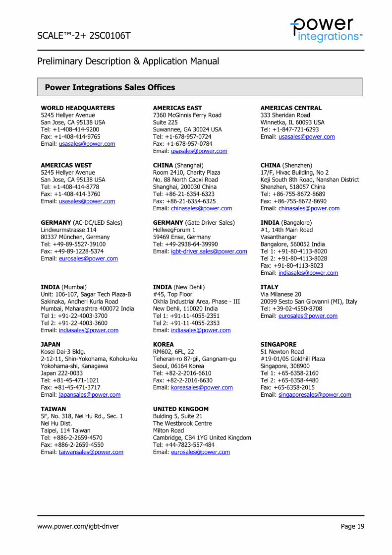
Power Integrations Sales Offices
WORLD HEADQUARTERS 5245 Hellyer Avenue San Jose, CA 95138 USA Tel: +1-408-414-9200 Fax: +1-408-414-9765 Email: [email protected]
AMERICAS EAST 7360 McGinnis Ferry Road Suite 225 Suwannee, GA 30024 USA Tel: +1-678-957-0724 Fax: +1-678-957-0784 Email: [email protected]
AMERICAS CENTRAL 333 Sheridan Road Winnetka, IL 60093 USA Tel: +1-847-721-6293 Email: [email protected]
AMERICAS WEST 5245 Hellyer Avenue
San Jose, CA 95138 USA Tel: +1-408-414-8778 Fax: +1-408-414-3760 Email: [email protected]
CHINA (Shanghai) Room 2410, Charity Plaza
No. 88 North Caoxi Road Shanghai, 200030 China Tel: +86-21-6354-6323 Fax: +86-21-6354-6325 Email: [email protected]
CHINA (Shenzhen) 17/F, Hivac Building, No 2
Keji South 8th Road, Nanshan District Shenzhen, 518057 China Tel: +86-755-8672-8689 Fax: +86-755-8672-8690 Email: [email protected]
GERMANY (AC-DC/LED Sales) Lindwurmstrasse 114 80337 München, Germany Tel: +49-89-5527-39100 Fax: +49-89-1228-5374 Email: [email protected]
GERMANY (Gate Driver Sales) HellwegForum 1 59469 Ense, Germany Tel: +49-2938-64-39990 Email: [email protected]
INDIA (Bangalore) #1, 14th Main Road Vasanthangar Bangalore, 560052 India Tel 1: +91-80-4113-8020 Tel 2: +91-80-4113-8028 Fax: +91-80-4113-8023 Email: [email protected]
INDIA (Mumbai) Unit: 106-107, Sagar Tech Plaza-B Sakinaka, Andheri Kurla Road Mumbai, Maharashtra 400072 India Tel 1: +91-22-4003-3700 Tel 2: +91-22-4003-3600 Email: [email protected]
INDIA (New Dehli) #45, Top Floor Okhla Industrial Area, Phase - III New Dehli, 110020 India Tel 1: +91-11-4055-2351 Tel 2: +91-11-4055-2353 Email: [email protected]
ITALY Via Milanese 20 20099 Sesto San Giovanni (MI), Italy Tel: +39-02-4550-8708 Email: [email protected]
JAPAN Kosei Dai-3 Bldg. 2-12-11, Shin-Yokohama, Kohoku-ku Yokohama-shi, Kanagawa Japan 222-0033 Tel: +81-45-471-1021 Fax: +81-45-471-3717 Email: [email protected]
KOREA RM602, 6FL, 22 Teheran-ro 87-gil, Gangnam-gu Seoul, 06164 Korea Tel: +82-2-2016-6610 Fax: +82-2-2016-6630 Email: [email protected]
SINGAPORE 51 Newton Road #19-01/05 Goldhill Plaza Singapore, 308900 Tel 1: +65-6358-2160 Tel 2: +65-6358-4480 Fax: +65-6358-2015 Email: [email protected]
TAIWAN 5F, No. 318, Nei Hu Rd., Sec. 1 Nei Hu Dist. Taipei, 114 Taiwan Tel: +886-2-2659-4570 Fax: +886-2-2659-4550 Email: [email protected]
UNITED KINGDOM Bulding 5, Suite 21 The Westbrook Centre Milton Road Cambridge, CB4 1YG United Kingdom Tel: +44-7823-557-484 Email: [email protected]