Embed Size (px)
Citation preview

13. System Architecture
Dezső Sima
Fall 2006
D. Sima, 2006
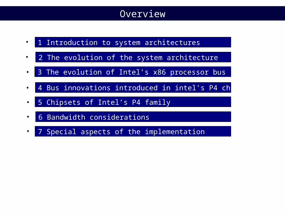
2 The evolution of the system architecture•
3 The evolution of Intel’s x86 processor bus•
5 Chipsets of Intel’s P4 family•
Overview
4 Bus innovations introduced in intel’s P4 chipsets•
1 Introduction to system architectures•
7 Special aspects of the implementation
• 6 Bandwidth considerations
•

Input latch
Booth encoder
Partialproduct
generation
PC
PC
PS
PS
Renormalise
Op A Op B
Halbstage 0
Halbstage 1
Halbstage 2
Halbstage 3
Partialproduct
generation
Input latch
Round
Add
FP-register file
PC: Product SumPS: Product Carry
FMUL
Decode, convertto uops
Map reg. numbers
Fetch operands
20RS
FMUL
FDIV
FADD
IU
IU
JEU AU AU
Memory Reorder Buffer
Store Load
Load Addr. Store Addr.Store Data
Shelve
Dispatch
Execute
IDIV
ISHF
Icache
128
I-buffer
D1 D2 D3 MIS
Reg. Mapping Table
1 uop/cycle4 uops/cycle
Port 0 Ports 3, 4Port 2Port 1
Feedback resultsfor updating
3 uops/cycle
Reg. numbers
Operands
RRF32
ROB32
Issue
JEUIU
(branch target address generation)
Integer UnitJump Execution Unit
AU Address Generation Unit:
:
D1 - D2
MISD3
DecodersGeneralised decoderMicroinstruction Sequencer:
::
:
FADD
IDIVISHF
FDIV
Integer Divide UnitInteger Shift UnitFP-AdderFP-Divider
FMUL
::::
3 uops/cycle
Fetch
FP-Multiplier:
Host bus
A.G.P. Bus82443LXPCI/A.G.P.Controller
(PAC)
Main Memory72 Bit
w/ECO 3.3V EDO &SDRAM Support
Graphicsadapter
Display
PCI Slots
Primary PCI Bus
(PCI Bus #0)
82371SB(PIIX4)
(PCI-to-ISABridge)
System Mgnt (SM) Bus
ISA Slots
ISA Bus
System BIOS
USBUSB
2 USB Ports
2 IDE Ports(Ultra DMA/33)
Pentium ProProcessor
operatingsystem
application program interface
Data carrier interface
Logical I/O interfaceUser interface
I/O controller
Application programming
data carrier
System level
Processor level
Functional unit level
Abstract architecture
Concrete architecture
Figure 1.1.: Interpretation of the notion architecture at different levels
1. Introduction
FMUL
Pentium Pro
Pentium Prosystem
OS
Pentium ProProcessor
ISA

2. The evolution of the system architecture
ISA-based
System architecture of Intel’s desktop PCs
Port-based
Simple w/ATA, USB
w/AGP,ATA,USB
PCI-based
8088/80286/80386-
based PCs
486 and earlyPentium
based PCs
Mature Pentium
based PCs
Early PIIand PIII
based PCs
MaturePIII/P4
based PCs
Intel 420chipsets
Mature Intel 430chipsets
Intel 440XXchipsets
Intel 8XXchipsets
Evolution
Early implem.
Recentimplem.
P4 Prescottbased PCs
Intel 915Xchipsets
2.1 System architecture of Intel’s desktop PCs - Overview

2.2 Main steps of the evolution (1)
Figure 2.1: ISA-bus based system architecture
(Used typically in 8088/80286/80386-based PCs)
8088/80286/80386Processor
Memory/Bus controller
Main MemoryKBD
FDAdapter
MonitorAdapter
WDAdapter
PPAdapter
SPAdapter
ISA
Multi-I/O card
(DRAM/FPM)
I/O devices

2.2 Main steps of the evolution (2)
Figure 2.2: Simple PCI-based system architecture
(Used typically in 486 and early Pentium-based PCs along with Intel 420 and early 430 chipsets)
486/Pentium
Systemcontroller
PCI bus
(Legacy and/or
Processor bus
L2 cache Main Memory(FPM/EDO)
Peripheralcontroller
PCI device adapter
ISA device adapter
ISA bus
slow devices)
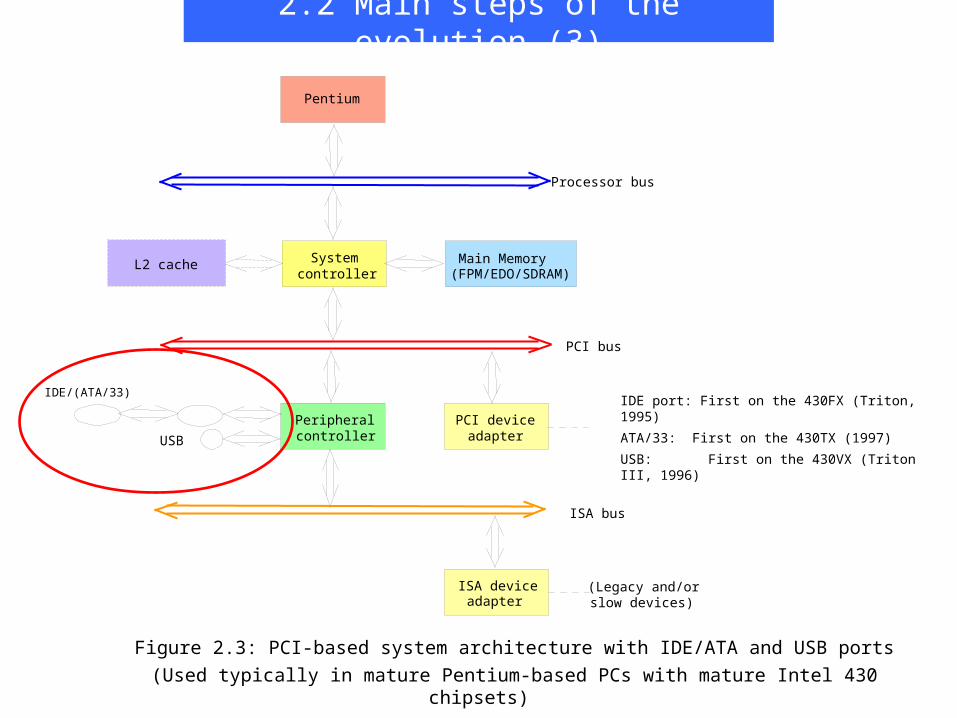
2.2 Main steps of the evolution (3)
Figure 2.3: PCI-based system architecture with IDE/ATA and USB ports
(Used typically in mature Pentium-based PCs with mature Intel 430 chipsets)
IDE port: First on the 430FX (Triton, 1995)
ATA/33: First on the 430TX (1997)
USB: First on the 430VX (Triton III, 1996)
Pentium
Systemcontroller
PCI bus
(Legacy and/or
Processor bus
L2 cache Main Memory (FPM/EDO/SDRAM)
Peripheralcontroller
PCI device adapter
ISA deviceadapter
ISA bus
slow devices)
USB
IDE/(ATA/33)

2.2 Main steps of the evolution (4)
Figure 2.4: PCI-based system architecture with AGP, IDE/ATA and USB ports(Used typically in PentiumII and early PentiumIII-based PCs with Intel 440XX
chipsets)
Systemcontroller
PCI bus
Processor bus
Main Memory(EDO/SDRAM)
Peripheralcontroller
PCI device adapter
ISA deviceadapter
ISA bus
PentiumII/
PentiumIIIPentiumII/
PentiumIII
AGP
2xIDE/ATA33/66
2xUSB
(Legacy and/orslow devices)

2.2 Main steps of the evolution (5)
Figure 2.5: Early port-based system architecture
(Used typically in PentiumIII and Pentium4-based systems with Intel
8X0 chipsets)
Systemcontroller
PCI bus
Processor bus
Main Memory (SDRAM/)
Peripheralcontroller
PCI device adapter
ISA deviceadapter
ISA bus
PentiumIII/
Pentiu4
AGP
2xIDE/
2x/4x USB
Hub interface
ATA 33/66/100
PCI to ISA bridge
LPC
Super I/O (KBD, MS, FD, SP, PP, IR)
AC'97
(Legacy and/orslow devices)

2.2 Main steps of the evolution (6)
Figure 2.6: Recent port-based system architecture
Systemcontroller
PCI bus
Processor bus
Main Memory (SDRAM/)
Peripheralcontroller
PCI device adapter
Pentium 4
PCI E.x16
1xIDE/
8x USB
Hub interface
ATA 33/66/100
LPC (KBD, MS, FD, SP, PP, IR)
AC'97
4x SATA
PCI E.x1 (1x/2x)
LAN 10/100
HDAI
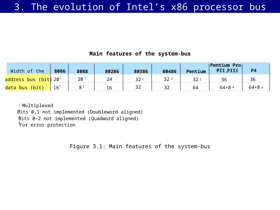
3. The evolution of Intel’s x86 processor bus
Figure 3.1: Main features of the system-bus
Main features of the system-bus
address bus (bit)
data bus (bit)
8086 8088 80286 80386 80486 PentiumPentium Pro
PII, PIII P4
20 20 24 32 32 32 36 36
16 8 16 32 32 64 64+864+8
MultiplexedBits 0,1 not implemented (Doubleword aligned)Bits 0-2 not implemented (Quadword aligned)
2
3
2 32
Width of the
1
4For error protection
1
1
1
1 4 4

Figure 4.1: Bus innovations introduced into Intel’s P4 chipsets
4. Bus innovations introduced into Intel’s P4 chipsets (1)
PCI
PCI-X
SATA
AGP
PCI Express
HDAI
USB
AC' 97
2001 2002 2003 2004
AC' 97 2.3
USB 2.0
AGP 8x
SATA 1.0a
PCI 2.3
PCI-X 2.2
PCI Express 1.0a
HDAI
11/02
5/03
5/03
2/04
6/04
5/02
12/01
6/04
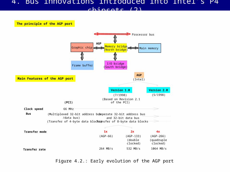
Figure 4.2.: Early evolution of the AGP port
4. Bus innovations introduced into Intel’s P4 chipsets (2)
Processor bus
Memory bridge(North bridge)
The principle of the AGP port
Frame bufferI/O bridge
(South bridge)
Graphic chip Main memory
AGP
(Intel)
Version 1.0 Version 2.0
(7/1998) (5/1998)
(Based on Revision 2.1 of the PCI)
66 MHz
Seperate 32-bit address busand 32-bit data bus
Transfer of 8-byte data blocks
1x 2x 4x
Clock speed
Bus
Transfer mode
Transfer rate
(Multiplexed 32-bit address bus/data bus)
(Transfer of 4-byte data blocks)
(PCI)
(AGP-66) (AGP-133) (AGP-266)(doubleclocked)
(quadrupleclocked)
264 MB/s 532 MB/s 1064 MB/s
Main Features of the AGP port
AGP
4. Bus innovations introduced into Intel’s P4 chipsets (3)
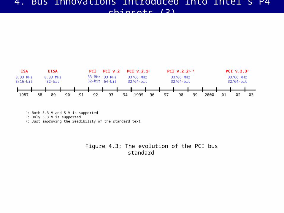
1987 88 89 90 91 92 93 94 1995 96 97 98 99 2000 01 02 03
ISA
8.33 MHz8/16-bit
EISA
8.33 MHz32-bit
PCI33 MHz32-bit
PCI v.2
33 MHz64-bit
PCI v.2.11
33/66 MHz32/64-bit
PCI v.2.32
33/66 MHz32/64-bit
PCI v.2.21, 3
33/66 MHz32/64-bit
1: Both 3.3 V and 5 V is supported2: Only 3.3 V is supported3: Just improving the readibility of the standard text
Figure 4.3: The evolution of the PCI bus standard
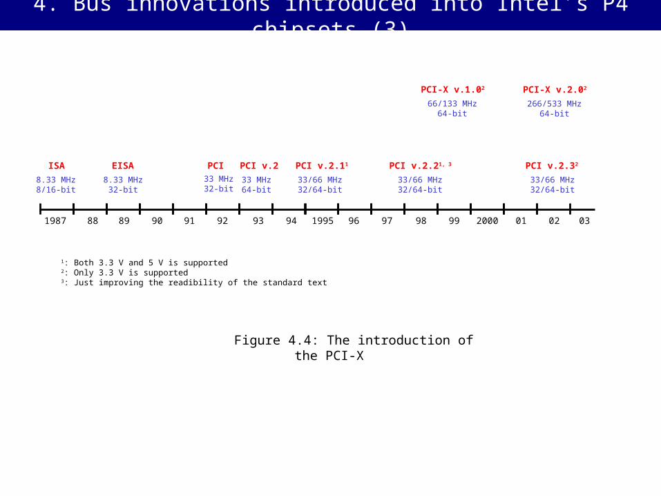
4. Bus innovations introduced into Intel’s P4 chipsets (3)
1987 88 89 90 91 92 93 94 1995 96 97 98 99 2000 01 02 03
PCI-X v.1.02
66/133 MHz64-bit
PCI-X v.2.02
266/533 MHz64-bit
1: Both 3.3 V and 5 V is supported2: Only 3.3 V is supported3: Just improving the readibility of the standard text
Figure 4.4: The introduction of the PCI-X
ISA
8.33 MHz8/16-bit
EISA
8.33 MHz32-bit
PCI33 MHz32-bit
PCI v.2
33 MHz64-bit
PCI v.2.11
33/66 MHz32/64-bit
PCI v.2.32
33/66 MHz32/64-bit
PCI v.2.21, 3
33/66 MHz32/64-bit

Source: PCI Technology overview, Febr. 2003, http://www.digi.com/pdf/prd_msc_pcitech.pdf
4. Bus innovations introduced into Intel’s P4 chipsets (5)
Figure 4.5: Slot number limitations of the PCI-X bus

4. Bus innovations introduced into Intel’s P4 chipsets (6)
• PCI Express 1.0 introduced in 7/2002
• A link consists of 1x, 2x, 4x, 8x, 12x, 16x or 32x signal pairs (lanes) in each direction.
• Transfer rate per lane per direction: 2.5 Gbits/s
• Encoding 10 bits/byte
Aggreagate bandwidth per lane (in both directions together):
2 x 2,5 /10 = 0,5 Gbyte/s
The PCI Express bus (3GIO)
4. Bus innovations introduced into Intel’s P4 chipsets (7)
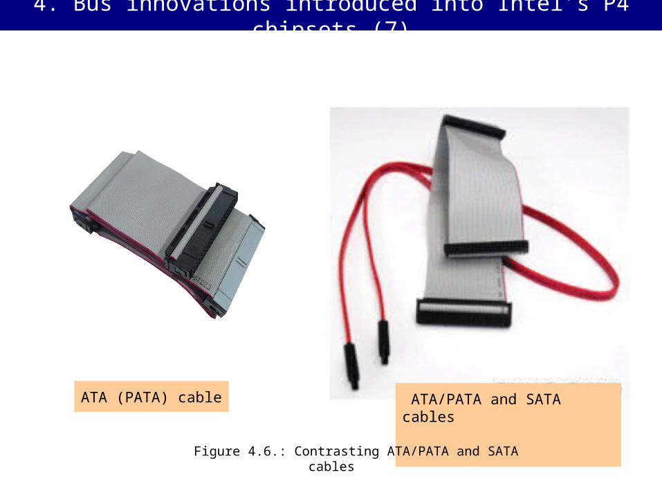
ATA (PATA) cable ATA/PATA and SATA cables
Figure 4.6.: Contrasting ATA/PATA and SATA cables

Figure 4.7.: Early evolution of the AC ’97 bus
4. Bus innovations introduced into Intel’s P4 chipsets (8)
AC '97
Version 1.0 Revision 2.1
(9/1997)
Version 2.0 Revision 2.2
(5/1998) (9/2000)6/1996: 5 vendors(Intel, ADI, Creative Labs,National Semiconductor,
Yamaha).
Link:5-wire digital(2 serial data lines)
Audio Codec16-bit optionally18/20-bit AD/DAresolution
48 KHz sampling rate4 analog stereo inputs2 analog mono inputs4/6 channel outputdedicated mic input
Digital controller
May reside on any bus(ISA, PCI, USB, 1394) orin an I/O-bridge
High Quality audio(up to 96 KHz sampling rate120 dB dynamic range)
Multiple codec
Modem extension(Cost effective)
capability (for multichannelaudio solutions etc.)

4. Bus innovations introduced into Intel’s P4 chipsets (9)
High definition audio (HDA)
No. of channels
Resolution
AC’97 v.2.2 HDAI
6
20-bit
Sampling rate 96 kHz
8
32-bit
192 kHz

AGP 4X
AGP 8X
VGA port
MbE c.
GbE c.
SCSI Ultra 320
Ultra ATA/100
SATA 1.0
PCI 32-bit/33 MHz
Peak bandwidth
PCI-X 64-bit/66 MHz
AC'97
MByte/s
1066
2132
12.5
125
320
100
150
133
~1.4
533
3/SDI, 6/SDOHDA
LPC
PCI-X 64-bit/133 MHz
PCI E. x1
PCI E. x4
PCI E. x8
PCI E. x16
USB 1.0
analog port
1066
500
2000
4000
8000
~5
USB 2.0
1.5
60
Sustained data rate up to
MByte/s
~125
60-90/drive, ~200-250/bus
~30-60/drive
~30-60/drive
~50
~400-450
Figure 4.8: Peak bandwidth values and sustained data rates of peripheral buses
4. Bus innovations introduced into Intel’s P4 chipsets (10)

5. Chipsets of Intel’s P4 family
5.1 Overview of the P4 family
5.2 Desktop chipsets
5.4 DP server chipsets
5.5 DP workstation chipsets
5.3 Overview of DP server and workstation chipsets
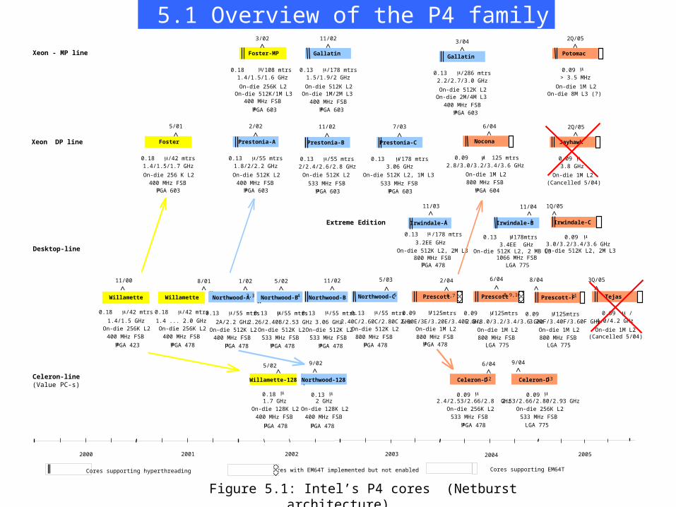
Figure 5.1: Intel’s P4 cores (Netburst
architecture)
5.1 Overview of the P4 family
11/00 1/02
^
0.18 /42 mtrs
^
400 MHz FSB
Northwood-A
Xeon DP line
Desktop-line
Celeron-line
Willamette
1.4/1.5 GHz
(Value PC-s)
On-die 256K L2
0.13 /55 mtrs
400 MHz FSB
2A/2.2 GHzOn-die 512K L2
2/02
^
0.13 /55 mtrs
400 MHz FSB
1.8/2/2.2 GHz
On-die 512K L2
5/01
^
0.18 /42 mtrs
400 MHz FSB
1.4/1.5/1.7 GHz
On-die 256 K L2
11/02
^Prestonia-B
0.13 /55 mtrs
533 MHz FSB
2/2.4/2.6/2.8 GHz
On-die 512K L2
Foster Prestonia-A Nocona
2/04
^
0.09 /125mtrs
800 MHz FSB
2.80E/3E/3.20E/3.40E GHzOn-die 1M L2
2000 2001 2002 2003 2004
Xeon - MP line
3/02
^
0.18 /108 mtrs
400 MHz FSB
1.4/1.5/1.6 GHz
On-die 256K L2
11/02
^Gallatin
0.13 /178 mtrs
400 MHz FSB
1.5/1.9/2 GHz
On-die 512K L2
Foster-MP
On-die 512K/1M L3 On-die 1M/2M L3
5/02
^Northwood-B
0.13 /55 mtrs
533 MHz FSB
2.26/2.40B/2.53 GHzOn-die 512K L2
5/02
^Willamette-128
400 MHz FSB
1.7 GHz
11/02
^
6/04
^
0.09 / 125 mtrs
800 MHz FSB
2.8/3.0/3.2/3.4/3.6 GHz
On-die 1M L2
Northwood-B
533 MHz FSB
3.06 GHzOn-die 512K L2
0.13 /55 mtrs
400 MHz FSB
2 GHz
On-die 128K L2
0.18 0.13
9/02
^Northwood-128
On-die 128K L2
Cores supporting hyperthreading
5/03
^Northwood-C
800 MHz FSB
2.40C/2.60C/2.80C GHzOn-die 512K L2
0.13 /55 mtrs
Cores with EM64T implemented but not enabled
2005
2Q/05
^Potomac
0.09 > 3.5 MHz
On-die 1M L2On-die 8M L3 (?)
Irwindale-C
1Q/05
^
0.09 3.0/3.2/3.4/3.6 GHz
On-die 512K L2, 2M L3
Jayhawk
2Q/05
^
0.09
(Cancelled 5/04)
3.8 GHz
On-die 1M L2
3Q/05
^Tejas
0.09 /4.0/4.2 GHz
On-die 1M L2(Cancelled 5/04)
Irwindale-A
11/03
^
800 MHz FSB
3.2EE GHz
On-die 512K L2, 2M L3
0.13 /178 mtrs
Cores supporting EM64T
6/04
^
0.09 /125mtrs
800 MHz FSB
2.8/3.0/3.2/3.4/3.6 GHz
On-die 1M L2
11/04
^Irwindale-B
0.13 /178mtrs
1066 MHz FSB
3.4EE GHzOn-die 512K L2, 2 MB L3
533 MHz FSB
2.4/2.53/2.66/2.8 GHz
On-die 256K L2
0.09
6/04
^Celeron-D
PGA 603 PGA 603
PGA 603 PGA 604
PGA 478 LGA 775
PGA 423 PGA 478 PGA 478 PGA 478 PGA 478 PGA 478 LGA 775
PGA 478 PGA 478
PGA 603 PGA 603
0.18 /42 mtrs
^
400 MHz FSB
Willamette
On-die 256K L2
PGA 478
3/04
^Gallatin
0.13 /286 mtrs
400 MHz FSB
2.2/2.7/3.0 GHz
On-die 512K L2On-die 2M/4M L3
PGA 603
8/01
PGA 478533 MHz FSB
2.53/2.66/2.80/2.93 GHz
On-die 256K L2
0.09
9/04
^Celeron-D
Extreme Edition
7/03
^Prestonia-C
0.13 /178 mtrs
533 MHz FSB
3.06 GHz
On-die 512K L2, 1M L3
PGA 603
1.4 ... 2.0 GHz0.09 /125mtrs
800 MHz FSB
3.20F/3.40F/3.60F GHz
On-die 1M L2
LGA 775
8/04
^
12 13
8,9,10PrescottPrescott Prescott-F 115 6,7
LGA 775
42,3
1 1

Figure 5.2: Intel’s chipsets designed for P4-based value and
desktop PCs
Chipsets
5/02
4/03
5/0310/02
6/04
8/03
5/03
9/03 5/03
9/03 6/04
FSB
Willamette
400 MHz 400 MHz 533 MHz 533 MHz
11/00
HTHT
Socket
Cores
EM64T
Northwood-A Northwood-B
Willamette
11/02
5/02
1/02
8/01
HT
400 MHz
EM64T
PGA 423 PGA 478 PGA 478 PGA 478 PGA 478
Northwood-C
800 MHz 800 MHz 800 MHz
5/03
HT HT
Prescott
Prescott6/04
2/04
800 MHz
HT
PGA 478 PGA 478 LGA 775 LGA 775
Prescott F
8/04
Northwood-B
845 G/E/GL
865P
845GV/GE/PE
848P
865G/GV/PE
875P
915G/GV/P
5.2 Desktop chipsets (1)
9/01
845
845
11/01

Figure 5.3: The evolution of Intel’s chipset families designed for P4-based value/mainstream desktops
5.2 Desktop chipsets (2)4/03 06/04
FSB up to
Memory
DRAM speed up to
Additional high speed
SATA
PCI
USB
845xx family 848P 865xx/875P family 915xx family
(Brookdale) (Springdale/Canterwood)
533 MT/s 800 MT/s 800 MT/s 800 MT/s
Single channel Single channel Dual channel Dual channel
SDR/DDR SDRAM DDR SDRAM DDR SDRAM DDR2 /DDR SDRAM
DDR 333 DDR 400 DDR 400 DDR 400/DDR2 533
CSA CSA
SATA 1.0a SATA 1.0a SATA 1.0a
PCI 2.2 PCI 2.3 PCI 2.3
USB 2.0 USB 2.0 USB 2.0 USB 2.0
5/02
no HT/HT HT HT HT
PCI 2.3
8/03 5/03
(Grantsdale)
HT support
Nr. of mem. channels
(unbuffered) (unbuffered)
LAN 10/100 Mbit/s
PCI Express x1
AC' 97 AC' 97 2.3 AC' 97 2.3 AC' 97 2.3 AC' 97 2.3
(unbuffered) (unbuffered)
MCH/GMCH
10/100 Mbit/s 10/100 Mbit/s 10/100 Mbit/s
HDAI HDAI
1
PCI Express x1 1.0a2
3
1
2
3
The Communications Streaming Architecture (CSA) interface of the MCH provides a link to a Gigabit Ethernet Controller (GbE), e.g. to Intel's 82547EI GbE controller
The Intel High Definition Audio Interface (HDAI) shares pins with the AC '97 link, so these interfaces cannot be operated concurrently
3
A GbE controller can be attached via the PCI Express x1 link providing 10/100/1000 Mbit/s speeds. (e.g. Intel's 82571EB dual channel GbE controller)
Max. memory 2 GB 2 GB 4 GB 4 GB
interface
845
400 MT/s
Single channel
SDR/DDR SDRAM
DDR 266
PCI 2.2
USB 1.1
9/01
no HT
(unbuffered)
10/100 Mbit/s
AC' 97 2.1
2 GB
11/05
975x
1066 MT/s
Dual channel
DDR2 SDRAM
DDR2 667
SATA 1.0a
USB 2.0
HT
PCI 2.3
(unbuffered)
AC' 97 2.3
ICH ICH4: ICH5/ICH5R: ICH5/ICH5R: ICH6/ICH6R:
Graphics interface up to AGP 4X AGP 8X AGP 8X PCI Express x16
ICH2:
AGP 4X
ICH7/ICH7R:
PCI Express x16
10/100 Mbit/s
HDAI
PCI Express x1 1.0a2
8 GB
ATA up to Ultra ATA/100 Ultra ATA/100 Ultra ATA/100 Ultra ATA/100Ultra ATA/100 Ultra ATA/100

Figure 5.4: The evolution of chipsets intended primarily for P4-based value/mainstream desktops
P4
ICH
ICH2/4/5/5R /6/6R
BIOS
MCH SDRAM
SDRAM
SDRAM
interface
SDRAM
interface
PC 133, DDR 200/266/333/400, DDR2 400/533
unbuffered, ECC opt.
3
3
The 865xx, 865 and 915xx chipsets have a dual channel memory link..
FSB
FWH
ATA/100
SATA
LAN 10/100
GPI0
LPC
PCI
PCI-X
PCI Express x1
USB
AC/97
HDAI
Max. 2/4 GB
HI 1.5/DMI
(845/845xx/848P/865xx/875P/915xx)AGP 4X/8X/PCI Express x.16
3
4
4 The 845 has a max. memory of 3 GB for SDR SDRAMs.5
6
5
ICH4 ICH5(R) ICH6(R)
4
6x v2.2 6x v2.3 7x v2.3
6x v2.0 8x v2.0 8x v2.0
v2.3 v2.3 v2.3
ICH2
6x v2.2
4x v1.1
v2.1
845xx 848P845865xx
915xx
875P
5 6
6
VGA1
2
1The chipsets including the letter G in their designation provide an integrated graphics controller.2 The chipsets including the letters GL or GV in their designation don't have an AGP or PCI Express x16 interface.
The ICH5R includes an integrated RAID controller that utilizes the dual SATA ports for a high performance RAID Level 0 implementation.
The ICH6R includes an integrated RAID controller that utilizes the dual SATA ports for a high performance RAID Level 0 implementation.
ICH4 ICH5(R) ICH6(R)
2
12
4
2
845xx 848P845865xx
915xx
ICH2
2
875P
5 6
5 6
5.2 Desktop chipsets (4)

Part. nr.
Interface to the MCH
ATA ports
SATA ports
PCI masters
PCI-X masters
PCI Express x1 ports
USB ports
LAN
AC' 97
HDAI
GPIO
LPC
Initial release
2x Ultra ATA/100 2x Ultra ATA/100 2x Ultra ATA/100 2x Ultra ATA/100 2x Ultra ATA/100 1x Ultra ATA/100
ICH2 ICH3S ICH4 ICH5/ICH5R 6300ESB ICH6/ICH6R
2x SATA 2x SATA 4x SATA
6x v. 2.2 6x v. 2.2 6x v. 2.2 6x v. 2.3 4x v. 2.2 7x v. 2.3
82801 BA 82801 CA 82801 DB 82801 EB/82801 ER
HI 1.5 HI 1.5 HI 1.5 HI 1.5 HI 1.5 DMI
4x v. 2.2
4x v. 1.0a
4x v. 1.1 6x v. 1.1 6x v. 2.0 8x v. 2.0 4x v. 2.0 8x v. 2.0
10/100 Mb/s 10/100 Mb/s 10/100 Mb/s 10/100 Mb/s 10/100 Mb/s
v. 2.1 v. 2.2 v. 2.3 v. 2.3 v. 2.2 v. 2.3
6/00 2/02 5/02 4/03 2/04 6/04
82801 FB/82801 FR
1
2
1
2
Each ATA port is capable to serve two ATA devices (a primary and a secondary device).
Each SATA port is capable to serve a single SATA device.
1x Ultra ATA/100
ICH7/ICH7R
4x SATA
6x v. 2.3
DMI
4/6x v. 1.0a
8x v. 2.0
10/100 Mb/s
v. 2.3
4/05
82801 FB/82801 FR
Figure 5.5: Main features of Intel’s I/O Control Hubs (ICH) used in P4-based chipsets
5.2 Desktop chipsets (3)

Figure 5.6: Intel’s chipsets designed for P4-based value and
desktop PCs
Chipsets
9/01
5/02
4/03
5/0310/02
6/04
8/03
5/03
9/03 5/03
9/03 6/04
FSB
Willamette
400 MHz 400 MHz 533 MHz 533 MHz
11/00
HTHT
Socket
Cores
EM64T
Northwood-A Northwood-B
Willamette
11/02
5/02
1/02
8/01
HT
400 MHz
EM64T
PGA 423 PGA 478 PGA 478 PGA 478 PGA 478
Northwood-C
800 MHz 800 MHz 800 MHz
5/03
HT HT
Prescott
Prescott6/04
2/04
800 MHz
HT
PGA 478 PGA 478 LGA 775 LGA 775
Prescott F
8/04
Northwood-B
845
845 G/E/GL
865P
845GV/GE/PE
848P
865G/GV/PE
875P
915G/GV/P
5.2 Desktop chipsets (1)
845
11/01
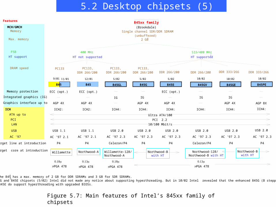
Figure 5.7: Main features of Intel’s 845xx family of chipsets
5/02 10/02
Graphics interface up to
845GL 845GV845G 845E 845GE
IG
400 MHz 533/400 MHz
AGP 4X AGP 4X
IG IG
10/02
845xx family(Brookdale)
10/100 Mbit/s
Ultra ATA/100
PCI 2.2
Single channel SDR/DDR SDRAM
AGP 4X
5/02
FSB
HT not supported HT supported
845
AGP 4X
IG
5/02 10/02
845PE
AGP 8X
PC133,DDR 266/200 DDR 266/200 DDR 266/200 DDR 333/266 DDR 333/266
Integrated graphics (IG)
AGP 4X
9/01 12/01
PC133 PC133,DDR 266/200
PC133,DDR 266/200
Memory protection ECC (opt.)ECC (opt.)ECC (opt.)
(unbuffered)
HT support
DRAM speed
ICH ICH4: ICH4: ICH4:ICH4:ICH2: ICH4:ICH2:
USB USB 2.0USB 1.1USB 1.1
ICH4:
USB 2.0 USB 2.0 USB 2.0 USB 2.0 USB 2.0
Features
Memory
ATA up to
PCI
LAN
AC '97 AC '97 2.3AC '97 2.1AC '97 2.1 AC '97 2.3 AC '97 2.3 AC '97 2.3 AC '97 2.3
MCH/GMCH
AC '97 2.3
Target line at introduction
Target core at introduction
P4 P4 P4 P4 Celeron/P4 P4 P4Celeron/P4
Willamette Willamette-128/Northwood-A
Northwood-A Northwood-Bwith HT
Northwood-Bwith HT
Northwood-128/ Northwood-B with HT
PGA 478
PGA 478 PGA 478 PGA 478
1
2
The 845 has a max. memory of 2 GB for DDR SDRAMs and 3 GB for SDR SDRAMs.
Max. memory 2 GB1
2At introduction of the 845G and 845E chipsets (5/02) Intel did not made any notice about supporting hyperthreading. But in 10/02 Intel revealed that the enhanced 845G (B stepping) and the original
845E do support hyperthreading with upgraded BIOSs.
5.2 Desktop chipsets (5)
11/01
845

Figure 5.8: Typical configuration of a value/desktop motherboard based on Intel’s 845xx family of chipsets
5.2 Desktop chipsets (6)
ICH4
FWH
SDRAMSDRAMinterface
DDR 200/266/333unbuffered, no ECC
Audio
GPIO
FSB
LPC
HI 1.5
P4Northwood
845xx
400/533 MHz
Max. 2 GB
GbE c.
LAN 10/100
GbE
PCI v.2.2
SIO
FD KB MS SP PP
(3-6 slots)
MbE c.MbE
USB 2.0(4-6 ports)
CODEC AC'97 v.2.3
AGP 4x
VGA
(G)MCH
1
1,21
2
The chipsets including the letter G in their designation provide an integrated VGA controller.
Mainboards based on the 845 chipset have a different configuration since they work with the ICH2.
3
Ultra ATA/100(2 ports)
PCI v.2.2
3 The chipsets 845GL/GV don't offer an AGP interface.
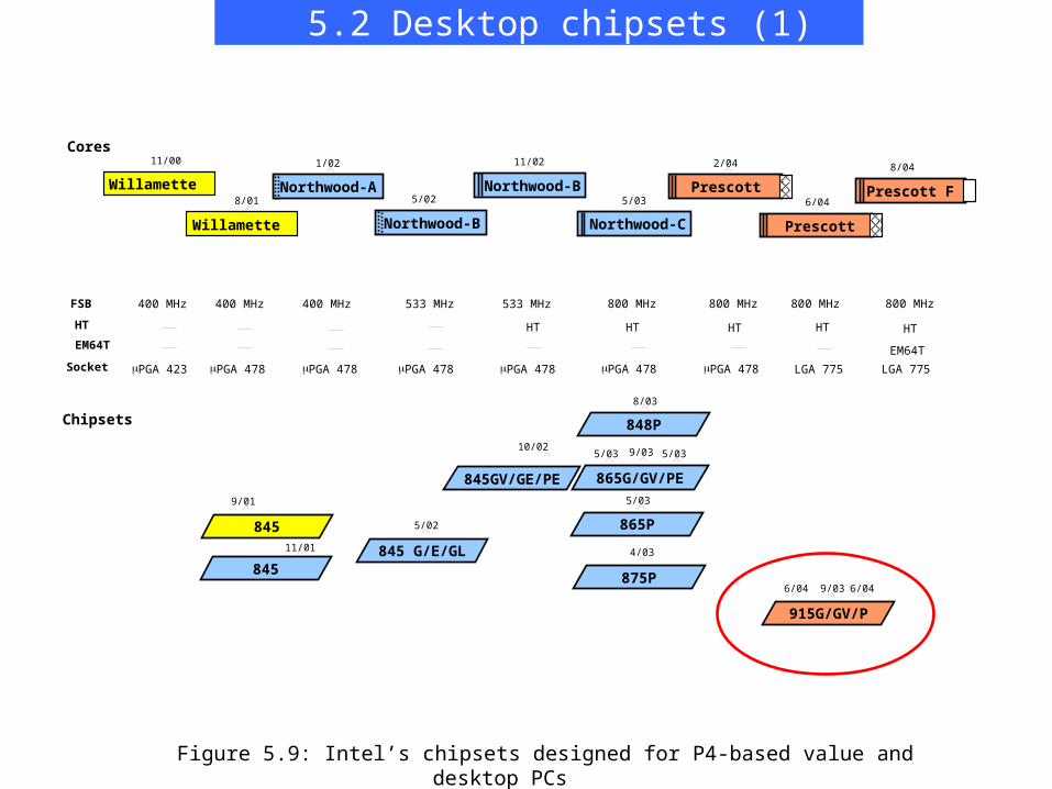
Figure 5.9: Intel’s chipsets designed for P4-based value and
desktop PCs
Chipsets
5/02
4/03
5/0310/02
6/04
8/03
5/03
9/03 5/03
9/03 6/04
FSB
Willamette
400 MHz 400 MHz 533 MHz 533 MHz
11/00
HTHT
Socket
Cores
EM64T
Northwood-A Northwood-B
Willamette
11/02
5/02
1/02
8/01
HT
400 MHz
EM64T
PGA 423 PGA 478 PGA 478 PGA 478 PGA 478
Northwood-C
800 MHz 800 MHz 800 MHz
5/03
HT HT
Prescott
Prescott6/04
2/04
800 MHz
HT
PGA 478 PGA 478 LGA 775 LGA 775
Prescott F
8/04
Northwood-B
845 G/E/GL
865P
845GV/GE/PE
848P
865G/GV/PE
875P
915G/GV/P
5.2 Desktop chipsets (1)
9/01
845
845
11/01

Figures 5.10: Main features of Intel’s 915xx family of chipsets
5.2 Desktop chipsets (7)
6/04
FSB
DRAM speed
Integrated graphics (IG)
Graphics interface up to
910GL 915P915G 915GV
(Grantsdale-G)
533 MHz 800/533 MHzDDR 400/333 DDR2 533/400, DDR 400/333
PCI Express x16PCI Express x16
(Grantsdale-P)
IG IG
6/04
915xx family
PCI 2.3
Ultra ATA/100
PCI Express x1 1.0a
HT supported
IG
9/04 9/04
Dual channel DDR2/DDR SDRAM(unbuffered, no ECC)
4
4
Supports processors also in socket PGA 478.
ICH6:
Features
HT supportMemory
ICHIDE up to
PCI ExpressPCI
MCH/GMCH
SATA SATA 1.0a
LANAC '97HDAI
10/100 Mbit/sAC '97 2.3
HDAI supported
(Grantsdale-V)(Grantsdale-GL)
2
2
A GbE controller can be attached via the PCI Express x1 link providing 10/100/1000 Mbit/s speeds (e.g. Intel's 82571EB dual channelGbE controller).
3
3
3
The Intel High Definition Audio Interface (HDAI) shares pins with the AC '97 link, so these interfaces cannot be operated concurrently.
Target line at introduction
Target core at introduction
Celeron /P4Celeron
Celeron D Celeron D/Prescott without EM64T
LGA 775
PGA 478/LGA 775
(Grantsdale)
1
Max. memory 4 GB
The max. memory of the 910GL is restricted only to 2 GB.
1

Figure 5.11: Typical configuration of a value/desktop motherboard based on Intel’s 915xx family of chipsets
5.2 Desktop chipsets (8)
1
2
The chipsets including the letter G in their designation provide an integrated VGA controller.
The 915GL/GV chipsets don't offer a PCI Express x16 interface.
ICH6
FWH
SDRAM
SDRAM
SDRAMinterface
SDRAMinterface
DDR 333/400, DDR2 400/533unbuffered, no ECC
Ultra ATA/100
PCI E. x1
Audio
GPIO
FSB
LPC
DMI
P4Prescott
915xx
533/800 MHz
Max. 4 GBPCI E. x16
MbE c.LAN 10/100
PCI E. x1
MbE
PCI v.2.3
SIO
FD KB MS SP PP
(1-2 ports)
(2-4 slots)
GbE c.GbE
USB 2.0(8 ports)
CODEC AC'97 v.2.3
SATA(4 ports)
PCI E. x16
VGA
(G)MCH
11
2
PCI v.2.3(1 port)
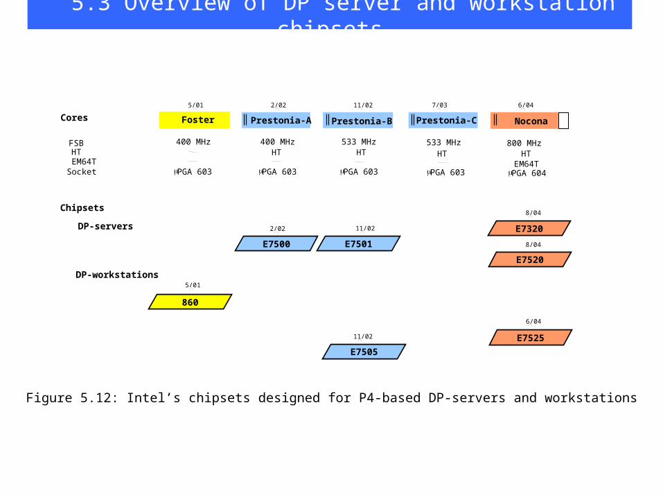
Figure 5.12: Intel’s chipsets designed for P4-based DP-servers and workstations
5.3 Overview of DP server and workstation chipsets
FSB
DP-servers
Foster
400 MHz 400 MHz 533 MHz 800 MHz
5/01
HT HTHT
Socket
Cores
EM64T
Prestonia-B Prestonia-C NoconaPrestonia-A
6/047/0311/022/02
HT
533 MHzHT
EM64TPGA 603 PGA 603 PGA 603 PGA 603 PGA 604
Chipsets
DP-workstations5/01
2/02
8/04
8/04
11/02
11/02
6/04
860
E7500 E7501
E7505
E7320
E7520
E7525

Figure 5.13: The evolution of Intel’s chipsets designed for P4 Xeon-based dual processor (DP) servers and workstations (WS)
5.4 DP server chipsets (1)
11/02 8/04
Graphics interface up to
PCI
PCI-X
E7500 E7320E7501 E7505 E7520
(Plumas)
400 MHz 533 MHz 800 MHz
1x PCI Express x8
PCI 2.2 PCI 2.2
(Lindenhurst-VS) (Lindenhurst)
8/04
E75xx/E73xx family
(registered, ECC)
Dual channel SDRAMHT supported
AGP 8X
2/02 11/02
DDR 266 /200DDR 200 DDR 333/266
6/04
E7525
DDR 333
(Tumwater)(Placer)
Aim DP server DP server DP WS DP server DP server DP WS
3x PCI Express x8
PCI Express x16
PCI 2.2 PCI 2.3/PCI 2.2
1 The 7505 supports also unbuffered DDR SDRAMs.
FSB
SATA SATA 1.0a SATA 1.0a SATA 1.0a
Features
HT support
IDE up to
EM64T supportedEM64T support
DRAM speed
ICH ICH3-S: ICH3-S: ICH4: ICH5R:/6300ESB: ICH5R:/6300ESB: ICH5R:/6300ESB:
PCI Express x1
AC' 97 AC '97 2.2
USB USB 1.1 USB 1.1 USB 2.0 USB 2.0 USB 2.0 USB 2.0
LAN 10/100 Mbit/s
/PCI-X 2.2 /PCI-X 2.2 /PCI-X 2.2
PCI 2.3/PCI 2.2 PCI 2.3/PCI 2.2
AC '97 2.3AC '97 2.2 AC '97 2.2/AC '97 2.3 AC '97 2.2/AC '97 2.3 AC '97 2.2/AC '97 2.3
10/100 Mbit/s10/100 Mbit/s 10/100 Mbit/s 10/100 Mbit/s 10/100 Mbit/s
MCH
RAS/RASUM RASUM RASUM RAS RASUM RASUM RASUM
400 MHz
AGP 4X
PCI 2.2
5/01
PC 800/600
DP WS
ICH2:
AC '97 2.1
USB 1.1
10/100 Mbit/s
860
ECC (opt.)
RDRAMDual channel
DDR2 400 DDR2 400
Target cores at introduction Foster Prestonia-A Prestonia-B Nocona
Technology/Socket PGA 603
2
2
The 7520 includes an integrated four channel DMA engine in contrast to the E7320.
PGA 603 PGA 604
Nr. of mem. channels
Memory
Memory protection
Ultra ATA/100 Ultra ATA/100 Ultra ATA/100 Ultra ATA/100 Ultra ATA/100 Ultra ATA/100 Ultra ATA/100
3x HI 2.0 3x HI 2.0Additional high speed if.
3
4
Max. memory 4 GB 16 GB1
1x PCI Express x81x HI 2.0
4
2x HI
3 3 3
4The ICH5R incorporates a RAID controller (Redundant Arrays of Indepentdent Disks) that utilizes the dual SATA ports for a high-performance RAID Level 0 configuration.
Reliability, Availability, Serviceability, Usability, Manageability
1
44
4
4
4 4

Figure 5.14: The evolution of DP-server chipsets of P4 cores
5.4 DP server chipsets (2)
1 The 16-bit HI 2.0 link is used to add PCI/PCI-X bridges (6700PXH), while the PCI Express x8 links are usually configured as two independent x4 ports,
each providing the possibility to add a PCI/PCI-X brigde (e.g. 6700PXH) or a dual GbE controller
2 Reliability, Availability, Serviceability, Usability, Manageability
3 The E7320 has only a single PCI Express x8 high speed interface
5 The ICH5R includes an integrated RAID controller that utilizes the dual SATA ports for a high performance RAID Level 0 implementation
4 An external SATA controller is needed only in connection with the ICH3-S
6 The 6300ESB SATA supports soft RAID.
P4
ICH
(ICH3-S/5R /6300ESB)
BIOS
MCH SDRAM
SDRAM
SDRAM
interface
SDRAM
interface
DDR 200/266/333/400, DDR2 400
registered, ECC
1
FSB
FWH
HI 1.5
P4
(E7500/7501/7320 /7520)
with RASUM2HI 2.0/PCI E. x8
HI 2.0/PCI E. x8
HI 2.0/PCI E. x8
5
SATA
ATA/100
LAN 10/100
GPI0
LPC
PCI
PCI-X
PCI Express x1
USB
AC' 97
HDAI
Max. 8-32 GB
3
High speed if.
Xeon Xeon
ICH3-S ICH5R 6300ESB
2 22
22
E7500
E7501
E7520 E3520
5
65
6ICH3-S ICH5R 6300ESB
4x v.2.2
6x v2.2 6x v2.3 4x v2.2
6x v1.1 8x v2.0 4x v2.0
E7500
E7501
E7520 E7320
v2.2 v2.3 v2.2
5 6

Figure 5.15: Typical configuration of a DP-server motherboard based on Intel’s E7500/E7501 chipsets
5.4 DP server chipsets (3)
P4
ICH3-S
FWH
E7500/E7501 SDRAM
SDRAM
SDRAMinterface
SDRAMinterface
DDR 200/266registered, ECC opt.
Ultra ATA/100
PCI v.2.2
USB v. 1.1
GPIO
FSB
LPC
HI 1.5
P4
(with RASUM)
HI 2.0
PCI-X v.2.2
Prestonia Prestonia
MCH
400/533 MHz
8/12/16 GBHI 2.0
HI 2.0
PCI-Xbridge
SATA c.
GbE c.
PCI-X v.2.2
SATA
GbE
Video c.
MbE c.PCI v.2.2
(5 ports)
SVGA
MbE
SIO
FD KB MS SP PP
SCSI c.SCSI
(1-2 slots)
(1-2 slots)
(3 slots)
(2 ports)
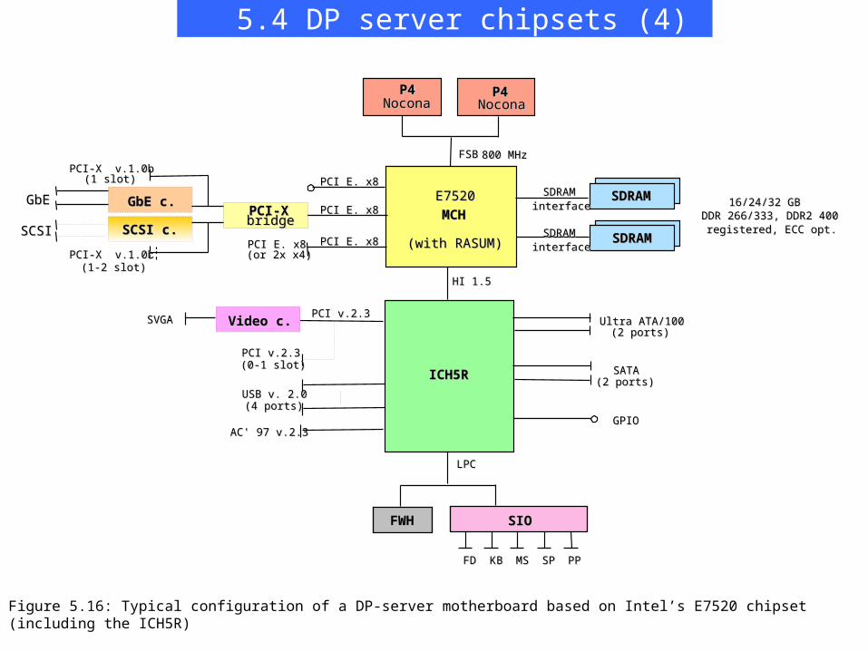
Figure 5.16: Typical configuration of a DP-server motherboard based on Intel’s E7520 chipset (including the ICH5R)
5.4 DP server chipsets (4)
P4P4
ICH5RICH5R
FWHFWH
E7520E7520 SDRAMSDRAM
SDRAMSDRAM
SDRAMSDRAMinterfaceinterface
SDRAMSDRAMinterfaceinterface
DDR 266/333, DDR2 400DDR 266/333, DDR2 400registered, ECC opt.registered, ECC opt.
Ultra ATA/100Ultra ATA/100
PCI v.2.3PCI v.2.3
USB v. 2.0USB v. 2.0
SATASATA
AC' 97 v.2.3AC' 97 v.2.3GPIOGPIO
FSBFSB
LPCLPC
HI 1.5HI 1.5
P4P4
(with RASUM)(with RASUM)
PCI E. x8PCI E. x8PCI-X v.1.0bPCI-X v.1.0b
NoconaNocona NoconaNocona
MCHMCH
800 MHz800 MHz
16/24/32 GB16/24/32 GBPCI E. x8PCI E. x8
PCI E. x8PCI E. x8
PCI-XPCI-Xbribridgdgee
SCSI c.SCSI c.
GbE c.GbE c.
PCI-X v.1.0bPCI-X v.1.0bPCI E. x8PCI E. x8(or 2x x4)(or 2x x4)
SCSISCSI
GbEGbE
Video c.Video c.PCI v.2.3PCI v.2.3
(4 ports)(4 ports)
SVGASVGA
SIOSIO
FDFD KBKB MSMS SPSP PPPP
(2 ports)(2 ports)
(2 ports)(2 ports)
(1 slot)(1 slot)
(1-2 slot)(1-2 slot)
(0-1 slot)(0-1 slot)

Figure 5.17: The evolution of DP-workstation chipsets of P4 cores
5.5 DP workstation chipsets (1)
P4
ICH
(ICH2/4/5R/6300ESB)
BIOS
MCH SDRAM
SDRAM
SDRAMinterface
SDRAMinterface
DDR 200/266/333, DDR2 400
registered, ECC opt.
1
1
The first chipsets of this line (the 860) worked with DRDRAMs while using PC 600/800.
FSB
FWH
HI 1.5
P4
(860 /E7505/7525)
with RASUM2
AGP 4X/8X/PCI E. x16
2Reliability, Availability, Serviceability, Usability, Manageability
3 The MCH of the 860 provides two 16-bit high speed interfaces, to add PCI v2.2 bridges (P64H).The ICH5R includes an integrated RAID controller that utilizes the dual SATA ports for a high performance RAID Level 0 implementation4
SATA
ATA
LAN 10/100
GPI0
LPC
PCI
PCI-X
PCI Express x1
USB
AC' 97
HDAI
2,3
XeonXeon
Max. 16 GB
ICH4 ICH5R 6300ESB
2 22
22
E7505
4
54
ICH2
2
860 E7525 E7525
5ICH4 ICH5R 6300ESB
4x v.2.2
6x v2.2 6x v2.3 4x v2.2
6x v2.0 8x v2.0 4x v2.0
v2.3 v2.3 v2.2
6x v2.2
4x v1.1
v2.1
ICH2
E7505860 E7525 E7525
4 5
The 6300ESB SATA supports soft RAID.5
HI 2.0, PCI E x8PCI-Xbridge
SCSISATAGbE

Figure 5.18: Typical configuration of a DP-workstation motherboard based on Intel’s E7505 chipset
5.5 DP workstation chipsets (2)
P4
FWH
E7505 SDRAM
SDRAM
SDRAM
interface
SDRAMinterface
DDR 200/266
registered, ECC opt.
Ultra ATA/100
GPIO
FSB
LPC
HI 1.5
P4
(with RASUM)
Prestonia B/C
MCH
533 MHz
8/12 GB
AGP 8x
SIO
FD KB MS SP PP
ICH4
Audio
MbE c.PCI v.2.2
MbE
PCI v.2.2
USB 2.0(4 ports)
CODECAC'97 v.2.2
Prestonia B/C
PCI-X v.2.2
HI 2.0PCI-X
SATA c.
GbE c.
PCI-X v.2.2
SATA
GbE
SCSI c.SCSI
(1-2 slots)
(1-2 slots)
bridge
(2 ports)
(1-2 slots)

Figure 5.19: Typical configuration of a DP-workstation motherboard based on Intel’s E7525 chipset
5.5 DP workstation chipsets (3)
P4
6300ESB
FWH
E7525 SDRAM
SDRAM
SDRAM
interface
SDRAM
interface
DDR 266/330registered, ECC opt.
Ultra ATA/100
GPIO
FSB
LPC
HI 1.5
P4
(with RASUM)
PCI E. x16
Nocona Nocona
MCH
800 MHz
16/24/32 GB
PCI E. x8
SIO
FD KB MS SP PP
ICH
SATAPCI-X v.2.2
Audio
GbE c.PCI-X v.2.2
GbE
PCI v.2.2
USB 2.0(4 ports)
CODECAC'97 v.2.2
(2 ports)
(2 ports)
PCI-XGbE c.
PCI-XGbE c. bridge
(2 slots)
x4
x4
(1-2 slots)

Source: Intel.com/products/I/chipsets/975x
5.6 Intel’s 975X chipset
Figure 5.20: Intel’s 975X chipset for dual core processors

Figure 6.1: Main features of the FSB and SDRAM interfaces
6. Bandwidth considerations (1)
FSB
SDRAM-interface
Width Peak aggregate bandwidth
64-bit 8 * f Mbyte/sc
64-bit 8 * f Mbyte/sSDRAM

HI 1.5
Used in the chipsets Width Peak aggregate bandwidth
All prior chipsets 266 MByte/s
DMI 910GL, 915xx, 925X, 925XE
8-bit
4*1 bit 2000 MByte/s
Figure 6.2: Main features of MCH/ICH interfaces used in Intel’s P4-based chipsets
6. Bandwidth considerations (2)

HI
CSA
HI 2.0
PCI E. x8
Used in the chipsets Width Peak aggregate bandwidth
860
848P/865xx/875P/E7210
16-bit
266 MByte/s
E7500/7501/7505
E7221/7320/7520/7525
16-bit
8-bit
8*1 bit
533 MByte/s
1066 MByte/s
4000 MByte/s
Figure 6.3: Main features of high speed MCH interfaces of Intel’s P4-based chipsets
6. Bandwidth considerations (3)

Figure 6.4: Peak bandwidth values (Mbyte/s) in typical desktops, based on Intel’s 865xx chipsets
ICH5
FWH
SDRAM
SDRAM
SDRAM
interface
SDRAM
interface
DDR 266/333/400
unbuffered, no ECC
Ultra ATA/100
Audio
GPIO
FSB 400/533/800 MHz
LPC
HI 1.5
P4Northwood B/C
865xx4 GB
MbE c.PCI v.2.3
CSA (HI 1.5)
MbE
PCI v.2.3
SIO
FD KB MS SP PP
(3 slots)
GbE c.GbE
USB 2.0(6-8 ports)
CODEC AC'97 v.2.3
SATA(2 ports)
AGP 8x
VGA
(GMCH)
1
2132
266
3200-6400
2132-3200
2132-3200
266
133
1.4
2*100
2*150
~5
(2 ports)
6. Bandwidth considerations (4)

Figure 6.5: Peak bandwidth values (Mbyte/s) in typical desktops, based on Intel’s 915xx chipsets
ICH6
FWH
SDRAM
SDRAM
SDRAMinterface
SDRAMinterface
DDR 333/400, DDR2 400/533
unbuffered, no ECC
Ultra ATA/100
PCI E. x1
Audio
GPIO
FSB
LPC
DMI
P4Prescott
915xx
533/800 MHz
4 GBPCI E. x16
MbE c.PCI v.2.3
PCI E. x1
MbE
PCI v.2.3
SIO
FD KB MS SP PP
(1-2 ports)
(2-4 slots)
GbE c.GbE
USB 2.0(8 ports)
CODEC AC'97 v.2.3
SATA(4 ports)
PCI E. x16
PCI E. x16
VGA
(G)MCH
18000
3200-6400
2664-4264
2664-4264
133
1.4
1*100
4*150
~5
500
500
60
8000
2000
(1 ports)
6. Bandwidth considerations (5)

Figure 6.6: Peak bandwidth values (Mbyte/s) in typical DP-servers, based on Intel’s E7500/E7501 chipsets
6. Bandwidth considerations (6)
P4
ICH3-S
FWH
E7500/E7501 SDRAM
SDRAM
SDRAMinterface
SDRAMinterface
DDR 200/266
registered, ECC opt.
Ultra ATA/100
PCI v.2.2
USB v. 1.1GPIO
FSB
LPC
HI 1.5
P4
(with RASUM)
HI 2.0
PCI-X v.2.2
Prestonia Prestonia
MCH
400/533 MHz
8/12/16 GB
HI 2.0
HI 2.0
PCI-Xbridge
SATA c.
GbE c.
PCI-X v.2.2
SATA
GbE
Video c.
MbE c.
PCI v.2.2
LAN
(5 ports)
SVGA
MbE
SIO
FD KB MS SP PP
SCSI c.SCSI
(1-2 slots)
(1-2 slots)
(3 slots)
3200-4264
1600-2128
1600-2128
266
133
1.5
2*100
~5
1066
1066
1066
(2 ports)

Figure 6.7: Peak bandwidth values (Mbyte/s) in typical DP-servers, based on Intel’s E7520/ICH5R chipset
6. Bandwidth considerations (7)
P4
ICH5R
FWH
E7520 SDRAM
SDRAM
SDRAMinterface
SDRAMinterface
DDR 266/333, DDR2 400
registered, ECC opt.
Ultra ATA/100
PCI v.2.3
USB v. 2.0
SATA
AC' 97 v.2.3
GPIO
FSB
LPC
HI 1.5
P4
(with RASUM)
PCI E. x8PCI-X v.1.0b
Nocona Nocona
MCH
800 MHz
16/24/32 GB
PCI E. x8
PCI E. x8
PCI-Xbridge
SCSI c.
GbE c.
PCI-X v.1.0bPCI E. x8(or 2x x4)
SCSI
GbE
Video c.
MbE c.
PCI v.2.3
LAN
(4 ports)
SVGA
MbE
SIO
FD KB MS SP PP
60
3200
2128-3200
2128-3200
266
133
~1.4
2*100
2*150
~5
4000
4000
4000
(2 ports)
(2 ports)
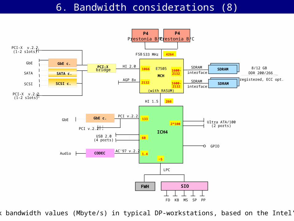
Figure 6.8: Peak bandwidth values (Mbyte/s) in typical DP-workstations, based on the Intel’s E7505 chipset
6. Bandwidth considerations (8)
P4
FWH
E7505 SDRAM
SDRAM
SDRAM
interface
SDRAM
interface
DDR 200/266
registered, ECC opt.
Ultra ATA/100
GPIO
FSB
LPC
HI 1.5
P4
(with RASUM)
Prestonia B/C
MCH
533 MHz
8/12 GB
AGP 8x
SIO
FD KB MS SP PP
ICH4
Audio
GbE c.PCI v.2.2
GbE
PCI v.2.2
USB 2.0(4 ports)
CODECAC'97 v.2.2
Prestonia B/C
PCI-X v.2.2
HI 2.0PCI-X
SATA c.
GbE c.
PCI-X v.2.2
SATA
GbE
SCSI c.SCSI
(1-2 slots)
(1-2 slots)
bridge
2132
133
4264
1600-2132
1600-2132
266
60
1.4
2*100
~5
1066
(2 ports)

Figure 6.9: Peak bandwidth values (Mbyte/s) in typical DP-workstations based on the Intel’s E7525 chipset
6. Bandwidth considerations (9)
P4
6300ESB
FWH
E7525 SDRAM
SDRAM
SDRAMinterface
SDRAMinterface
DDR 266/333
registered, ECC opt.
Ultra ATA/100
GPIO
FSB
LPC
HI 1.5
P4
(with RASUM)
PCI E. x16
Nocona Nocona
MCH
800 MHz
16/24/32 GB
PCI E. x8
SIO
FD KB MS SP PP
ICH
SATA
PCI-X v.2.2
Audio
GbE c.PCI-X v.2.2
GbE
PCI v.2.2
USB 2.0(4 ports)
CODEC AC'97 v.2.2
8000
4000
3.2-6.4
2132-2664
2132-2664
266
133
1.4
2*100
2*150
~5
60
533 (2 ports)
(2 ports)

7.1 Attaching the display
7.5 Implementation of ICHs
7.4 Attaching SCSI controllers
7.3 Attaching MbE/GbE controllers
7.2 PCI-X bridges
7. Special aspects of the implementation

7.1 Attaching the display
Figure 7.1: Alternatives for attaching a display in P4-based motherboards
Typical use:
P4
MCH
ICH
VGA
Value/mainstream desktopswith the letter G in their designation (e.g. 845G/GL/GV)
Entry level servers based onthe E7221
P4 P4
Off-boardMCH
ICH
AGP 4x/8x/
PCI E. x8/x16video c.VGA
Value/mainstream desktopsexcluding those with the lettersGL or GV in their designation
High end desktops/entry levelworkstations
DP-workstations
(e.g. 845GL/GV)
P4 P4
MCH
ICHPCI
32 bit/33 MHzvideo c.VGA
(mostly ATI Rage XL)
Entry level servers based on the E7210
DP-servers
On-board
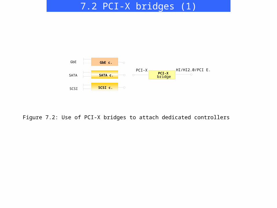
Figure 7.2: Use of PCI-X bridges to attach dedicated controllers
7.2 PCI-X bridges (1)
PCI-XSATA c.
GbE c.
SATA
GbE
SCSI c.SCSI
bridge
PCI-X HI/HI2.0/PCI E.
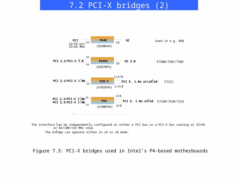
Figure 7.3: PCI-X bridges used in Intel’s P4-based motherboards
7.2 PCI-X bridges (2)
P64H16
HIPCI32/64-bit
33/66 MHz
64
(82806AA)
P64H216
HI 2.0PCI 2.2/PCI-X 1.064
(82870P2)
PXH-V
1/4/8
PCI E. 1.0a x1/x4/x8
64
(6702PXH)
PXH
64
(6700PXH)
PCI E. 1.0a x4/x8
1/4/8
64
PCI 2.3/PCI-X 1.0b
1
64
1
PCI 2.3/PCI-X 1.0b1
4/8
4/8
Used in e.g. 860
E7500/7501/7505
E7221
E7320/7520/7525
1
2
2
2
The interface can be independently configured as either a PCI bus or a PCI-X bus running at 33/66 or 66/100/133 MHz resp.
The bridge can operate either in x4 or x8 mode.
PCI 2.3/PCI-X 1.0b1
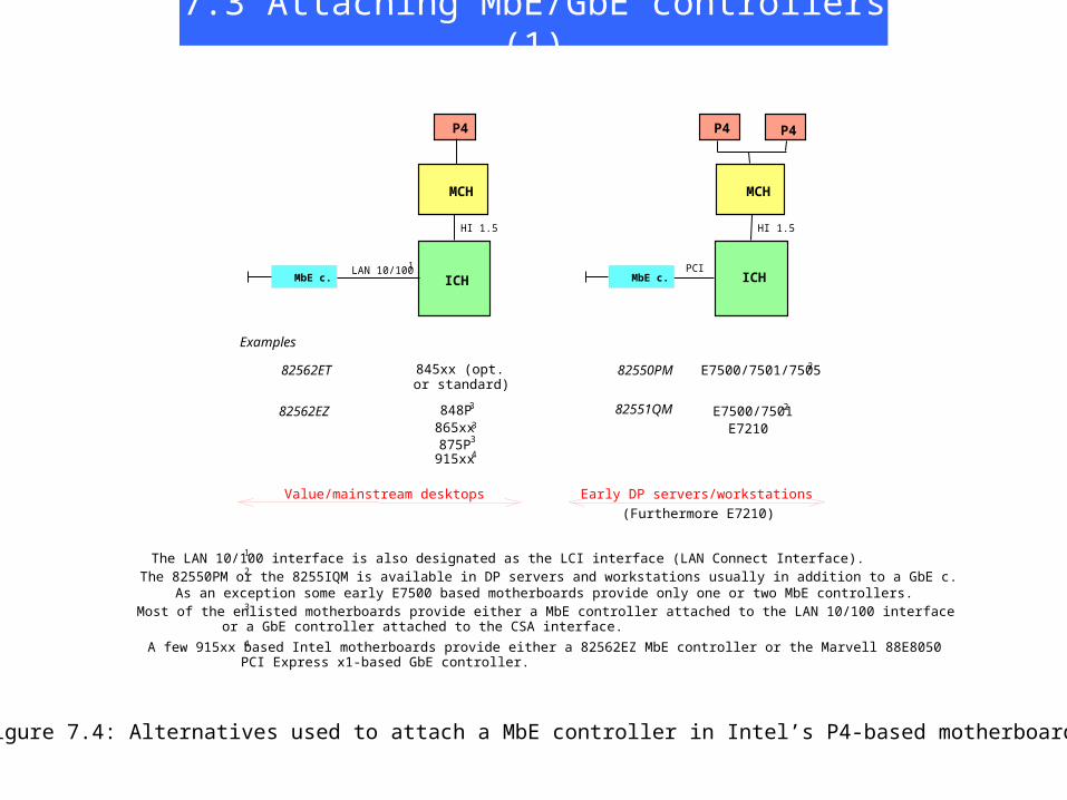
Figure 7.4: Alternatives used to attach a MbE controller in Intel’s P4-based motherboards
7.3 Attaching MbE/GbE controllers (1)
1
2
Examples
82550PM
82551QM
E7500/7501/7505
E7500/7501E7210
MCH
ICHMbE c.PCI
HI 1.5
2
2
3
82562ET 845xx (opt.
MCH
ICHMbE c.
P4
82562EZ 848P865xx875P915xx
HI 1.5
LAN 10/1001
3
3
3
4
4
The LAN 10/100 interface is also designated as the LCI interface (LAN Connect Interface).The 82550PM or the 8255IQM is available in DP servers and workstations usually in addition to a GbE c.
As an exception some early E7500 based motherboards provide only one or two MbE controllers.Most of the enlisted motherboards provide either a MbE controller attached to the LAN 10/100 interface
or a GbE controller attached to the CSA interface.
A few 915xx based Intel motherboards provide either a 82562EZ MbE controller or the Marvell 88E8050 PCI Express x1-based GbE controller.
P4 P4
Value/mainstream desktops Early DP servers/workstations
(Furthermore E7210)
or standard)

Figure 7.5: Widely used alternatives to attach a GbE controller in Intel’s P4-based motherboards via legacy buses
7.3 Attaching MbE/GbE controllers (2)
Examples
82540EM
82541GI
82541PI
845xxE7501
875P915xx925XE7210
E7221
MCH
ICH
PCI-XPCI-XGbE c.GbE brigde
P4 P4
HI 2.0
HI 1.5
82545EM
82546EB (D)
E7500/7501/7505
E7500/7501/7505
P4
MCH
ICHGbE c.PCI
GbE
HI 1.5
E7205
E7520(w/ICH5R)
P4
MCH
ICH
GbE c.CSA
GbE
HI 1.5
82547EI 848P865xx875P
E7210875P82547GI
1
1
2
3
5
4
5
4
4
4
Ususally in companion with a MbE controller such as the 82550PM or the 82551QM.
Ususally in companion with a MbE controller such as the 82551QM.
The 82541PI and the 8254GB is used in the 32-bit/33 MHz mode.
The 82541GI is used either in 32-bit/33MHz or 32-bit/66 MHz mode.
Most of the enlisted motherboards provide either a MbE controller attached to the LAN 10/100 interface or a GbE controller attached to the CSA interface.
82541GI
P4
MCH
ICHGbE c.
PCI-XGbE
P4
(6300ESB)
HI 1.5
Advanced DP servers/workstations
E7320/7525 (w/6300ESB)
82541GB E7320/7525 (w/6300ESB)
82541PI E7320/7525 (w/6300ESB)
2
3
3
Early DP servers/workstationsAll categories Mainstream desktops
(Furthermore the E7210)
7.3 Attaching MbE/GbE controllers (3)
Figure 7.6: Alternatives used to attach a GbE controller inIntel’s P4-based motherboards via the PCI Express bus
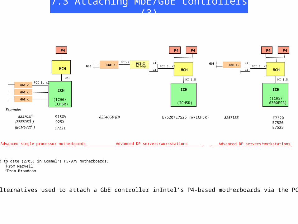
Examples
82570EI
(BCM5721 )
915GV
E7221
MCH
ICH
P4
MCH
ICH
GbE c.PCI E. x1
P4
82546GB (D) E7520/E7525 (w/ICH5R)
HI 1.5DMI
1
2
2
1
3
3
Used to date (2/05) in Commel's FS-979 motherboards.From MarvellFrom Broadcom
GbE c.
GbE c. (ICH6/ICH6R)
(88E8050 ) 925X
P4
PCI-XPCI E. x8
(ICH5R)
x4
x4
MCH
ICH
P4
82571EB E7320E7520E7525
HI 1.5
P4
GbE c.GbEPCI E. x8
(ICH5/6300ESB)
x4
x4GbE c.GbE bridge
PCI-X
Advanced DP servers/workstationsAdvanced single processor motherboards Advanced DP servers/workstations

Figure 7.7: Alternatives used to attach a SCSI controller in Intel’s P4-based motherboardsRemark: A few entry-level servers and DP-workstations incorporate also a SCSI controller,
like some based on the E7221 or E7505 chipsets
7.4 Attaching SCSI controllers
Typical use:
MCH
ICH
PCI-X
P4
Adaptec A16-7899W
P4
MCH
ICH
P4 P4
MCH
ICH
(Ultra 160, dual channel)
(Ultra 320, single channel)
(Ultra 320, dual channel)
LSI Logic 53C1020(Ultra 320, single channel)
Adaptec AIC-7902
LSI Logic 53C1030
P4 P4
HI 2.0
PCI-XbridgeSCSI c.
(P64H2)(E7500/7501)
PCI-X
PCI-XbridgeSCSI c.
(PXH-V)
x8
(E7320)
PCI-X
PCI-XbridgeSCSI c.
(PXH)
PCI E. x8 PCI E. x8
(E7520)
Advanced high-end DP-serversEarly DP-servers Advanced mid-range DP-servers
Adaptec AIC-7901
Adaptec AIC-7902
(Ultra 320, dual channel)
(Ultra 320, dual channel)
FSB FSB FSB

7.5 Implementation of ICHs (1)
Figure 7.8: Simplified structure of the ICH4
to (G)MCHHI 1.58-bit/66 MHz*4
Multiplexer
D:8, F0
32-bit/33 MHz
LAN 10/100D:29, F0
USB UHCI c. #1
D:29, F1USB UHCI c. #2
D:29, F2USB UHCI c. #3
D:29, F7USB 2.0 EHCI c.
D:30, F0PCI HUB/PCI bridge
D:31, F0LPC LPC bridge
D:31, F1ATAATA c.
D:31, F3SMBus SMBus
USB 2.0(2 ports)
USB 2.0(2 ports)
USB 2.0(2 ports)
(2 port)
ICH4
D: DeviceF: FunctionUHCI: Universal Host Controller InterfaceEHCI: Enhanced Host Controller Interface
LAN 10/100
(6 master)
D:31, F5AC'97 Audio c.
D:31, F6AC'97 v. 2.3
AC'97 0 Modem c.
PCI Bus 132-bit/33 MHz
PCI Bus 0

7.5 Implementation of ICHs (2)
Figure 7.9: Simplified structure of the ICH6
to (G)MCHDMI4*1-bit/2.5 GHz
Multiplexer
D8, F0
PCI Bus 132-bit/33 MHz
LAN 10/100D27, F0IHDA/AC'97 v.2.3
IHDA/AC'97 c.
D28, F0PCI E. X1 v1.0aPCI E. port 1
D28, F1PCI E. x1 v1.0aPCI E. port 2
D28, F2PCI E. x1 v1.0a PCI E. port 3
D28, F3PCI E. x1. v1.0a
PCI E. port 4
D29, F0USB 2.0USB UHCI c.
D29, F1USB UHCI c.
D29, F2USB UHCI c.
D29, F3USB UHCI c.
D29, F7USB 2.0 EHCI c.
D30, F0PCI v.2.3 PCI to PCI bridge
D30, F2AC'97 Audio c.
D30, F3AC'97/IHDA
AC'97 Modem c.
D31, F0LPC LPC c.
D31, F1ATAATA c.
D31, F2SATASATA c.
D31, F3SMBus
SMBus c.
(2 ports)
USB 2.0(2 ports)
USB 2.0(2 ports)
USB 2.0(2 ports)
(1 port)
(4 port)
ICH6
D: DeviceF: FunctionUHCI: Universal Host Controller InterfaceEHCI: Enhanced Host Controller Interface
LAN 10/100
PCI Bus 032-bit/33 MHz