Embed Size (px)
Citation preview

9-1- 1

9-1- 2
2. 1.3 GHz SRF Cavities
There are currently two main types of 1.3 GHz SRF cavities that are in large scale use for accelerators:
2.1. Tesla cavities
The Tesla cavity is 9-cell standing wave structure of about 1 m length whose lowest TM mode resonates at 1300 MHz, as seen in Fig. 2. The shape of the cavity is influenced by many factors like to lower peak electric field the iris needs to be rounded, and peak magnetic field considerations requires rounding of the equator region (larger diameter of cell), where the magnetic field is the strongest and needs to be weakened significantly. Multipacting is also a key factor that governs the overall rounded contour of the cavity profile. If the shape is not rounded, one-surface multipacting will severely limit the cavity performance. Moreover, elliptical arc segments of cell increase the strength of the cavity against atmospheric load and also provide a slope for efficient draining and rinsing of liquids during surface etching and cleaning in vertical orientation [3].
Fig. 2 1.3 GHz 9-Cell Niobium Superconducting Tesla cavity [2]
The cavity is equipped with its own Titanium tank or jacket, a tuning system driven by a stepper motor, a coaxial rf power coupler capable of transmitting more than 200 kW, a pickup antenna and two higher order mode couplers, as seen in Fig. 3 and 4 [4]. It is cooled with 2.0 K superfluid helium (He II) which is another phase of liquid helium when cooled below 2.17 K. This is considered as an optimal temperature range considering the
refrigeration cost, BCS losses and Carnot efficiency.
Fig. 3 1.3 GHz 9-Cell Niobium Superconducting Tesla cavity assembly (Rey.hori©)
The largest accelerator using the cavities with this design is the European Free Electron Laser (Eu-XFEL). It is a 2.1 km superconducting Linac to accelerate electron to 17 GeV by using 808 1.3 GHz 9-Cell SRF cavities. The cavity design performance for the Eu-XFEL required an average Eacc ≥ 23.6 MV/m at a Q0 ≥ 1 × 10^10 [4]. Design of the Eu-XFEL’s 1.3 GHz Tesla cavity assembly is shown in the Fig. 4.
Fig. 4 Tesla cavity assemble at Eu-XFEL DESY (top) and its cut view (below) [4]

9-1- 3
2.2. Tesla-like cavities
There were some modifications and optimizations made at KEK in the design of Tesla cavities and was named as Tesla-like cavity. The modifications are listed below and are shown in Fig. 5 [5]:
• Improved support stiffness: Thick Ti end plates improved the stiffness of the cavity support structure. This is to suppress cell shrinkage in the axial direction due to the Lorentz force in a pulsed operation.
• Enlarged beams pipe diameter: To compensate for the weakened input coupling due to the thick end plates.
• Enlarged input port diameter: To enlarge the RF window for improved power capability.
• Optimization of cell shape: To decrease the ratio of the surface peak magnetic field to the accelerating gradient.
• Installation of magnetic shield inside the helium vessel.
Fig. 5 Comparison between cavities structures Tesla cavity at DESY (top) and Tesla-like at KEK (below) [5]
3. Materials for SRF Cavity Assembly
3.1. Niobium (1.3 GHz SRF Cavity)
Niobium (Nb) has a body-centred cubic (bcc) crystal structure and a melting point of 2,468 °C. Among others, its low density in comparison to other refractory metals, its corrosion resistance, its superconductivity properties and its capability for forming dielectric oxide layers, have made niobium a material of choice in many different fields [6]. For these reasons, niobium-based alloys are often used in aerospace and medical applications. However, the vast majority of Nb reduced from raw ores are used as an alloying element for steels. Moreover, because of its strengthening effect at elevated temperatures, its principal commercial use is as an additive in steels and super alloys like carbon steels, new X-series of alloys for pipeline construction etc. [7]. Niobium-titanium and niobium-tin alloys are also used as superconducting materials. For particle accelerators, the Niobium’s superconductivity at 9.2 K makes it ideally suited for the construction of SRF cavities for high energy physics.
3.2. Mining of Niobium
Niobium and tantalum always occur in association with one another in nature. The main mineral, pyrochlore, is mostly processed by primarily physical processing technology to obtain niobium oxide, with a concentration from 55% to about 60%. The most important reserves are calcium niobate from Brazil (about 80%) and Canada (about 10%), and stibiotantalite from West Australia. The second most important source of Nb producing ore is niobite (columbite) – tantalite [(Fe,Mn)(Nb,Ta)2O6]. When tantalum significantly exceeds niobium by weight, it is tantalite; and when niobium

9-1- 4
significantly exceeds tantalum by weight, it is columbite. As a mineral with a ratio of Nb2O5:Ta2O5 from 10:1 to 13:1, columbite occurs in Brazil, Nigeria, and Australia, as well as other countries of Central Africa. Usually, niobium is recovered when the ores are processed for tantalum [8].
The world’s largest niobium deposit, located in Araxá, Brazil, is owned by Companhia Brasileira de Metalurgia e Mineração (CBMM). The reserves are enough to supply current world demand for about 500 years, about 460 million tons. The weathered ore mine contents are between 2.5 and 3.0% Nb2O5. The mining is carried out by open-pit extraction. The ore is crushed and magnetite is magnetically separated from the pyrochlore. By chemical processes, the ore is concentrated with regard to its Nb content (50–60% of Nb2O5) [8].
3.3. Purification of Niobium
The melting and purification of Niobium is conducted by an electron beam furnace. It is an efficient and reliable methodology conducted in vacuum of < 3E-3 mbar for the first melt and < 1E-6 mbar for last melt to obtain high purity Nb [8]. During the melting process the molten globules drop into water cooled copper crucible to form an ingot. The material is pressed to form and the ingot to be fed vertically for remelting for purification under vacuum, as shown in Fig 6. During the melting process the gases and impurities with lower melting temperatures than Nb evaporates. Most of the times the impurities on top of the ingot are higher than the bottom of the Ingot and is non-homogenous. Although, most of the impurities are present on the skin of the ingot which can be machined away for a purer ingot.
Fig. 6 Schematic of drip melting in an electron beam melting furnace (top) [8]; Intermediate Nb ingot ready for re-melting [9] (below)
At CBMM, there are two furnaces that are used to produce pure Nb (high RRR). A Leybold furnace with 500 kW nominal power and 50,000 liter per second pumping capacity melts the Niobium from 40 – 50 kg/hr, and another 1.8 MW nominal power and 150,000 liters per second pumping capacity melts with 90 – 120 kg/hr and pressures < 1E-3 mbar [6]. There are several companies that can produce high purity refractory metals in larger quantities: ATI Wah Chang (USA), Cabot (USA), W.C. Heraeus (Germany), Tokyo Denkai (Japan), Ningxia (China), CBMM (Brazil), H.C. Starck (Germany, USA). A picture of electron beam melting furnace at ATI Wah Chang is shown in Fig. 7.
The main impurities that significantly effects the properties of the Nb are O, N, C and H. The level of O, N and C should be < 10 ppm and H < 1 ppm to achieve high residual resistivity ratio (RRR) > 300.

9-1- 5
Fig. 7 Electron beam melting furnace at ATI Wah Chang Company [9]
3.4. Post-purification
The cavity processing techniques such as high-pressure rinsing, chemical polishing and electro-polishing can instill impurities such as hydrogen, hence further purification is required. The commonly used technique is hydrogen degassing by annealing the cavities at high temperatures.
3.4.1. Hydrogen Degassing
Hydrogen can dissolve in the bulk material at room temperature at a rate of several mm/hr. The concentration of hydrogen tends to be higher near the surfaces, interfaces and crystal defects. Higher concentration of hydrogen has been known to cause “Q-disease” in SRF cavities where the Q0 of the cavity degrades significantly. To avoid this there are two ways: either cool the cavity rapidly in the cryostat through 75 K < T < 150 K region to avoid precipitation of ε-phase or degas the cavities at higher temperatures > 500 °C under vacuum conditions. Fast cooling is not a permanent fix,
hence degassing is preferable in surface preparation [10].
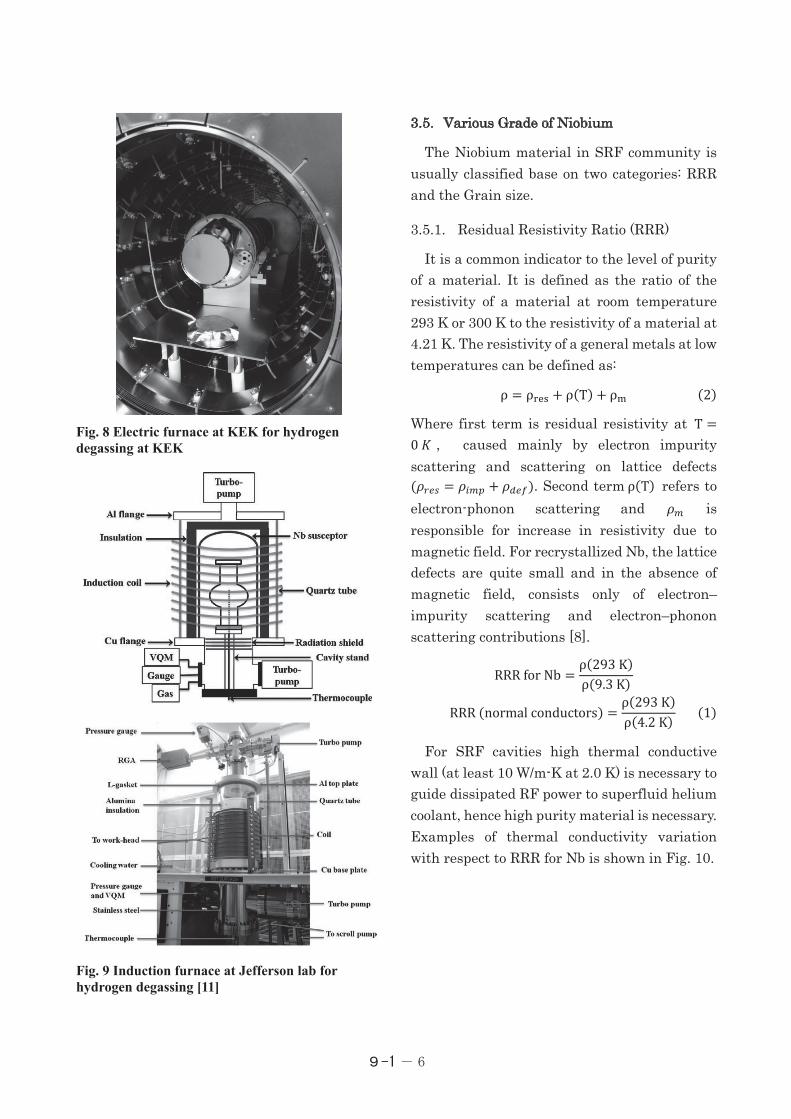
Hydrogen degassing is basically a form of high temperature treatment of Nb, where Niobium is placed in an electric or induction furnace under a vacuum pressure of < 10-3 Pa. The electric furnace used for the high-temperature heat treatment of SRF cavities is an ultra-high-vacuum furnace with molybdenum hot-zones of molybdenum (or tungsten) resistive heating elements, and the cavities are heated by radiation from the heating elements. The ultra-high vacuum inside the furnace is created with cryo-pumps, an example of electric vacuum furnace at KEK is shown in Fig. 8.
In the case of ultra-high vacuum induction furnace, the hot zone is made of Niobium and the cavity is treated by black-body radiation. It makes use of Cu induction coil to instill eddy current in the Niobium, to produce heat from the electric resistance of the material, as shown in Fig 9.
In many facilities like KEK (Tesla-like), Eu-XFEL, LCLS II etc. hydrogen degassing is conducted at 800 °C for 2-3 hours. However, this being a form of annealing does degrade the mechanical properties of the Niobium, which will be shown in later sections.
9-1- 6
Fig. 8 Electric furnace at KEK for hydrogen degassing at KEK
Fig. 9 Induction furnace at Jefferson lab for hydrogen degassing [11]
3.5. Various Grade of Niobium
The Niobium material in SRF community is usually classified base on two categories: RRR and the Grain size.
3.5.1. Residual Resistivity Ratio (RRR)
It is a common indicator to the level of purity of a material. It is defined as the ratio of the resistivity of a material at room temperature 293 K or 300 K to the resistivity of a material at 4.21 K. The resistivity of a general metals at low temperatures can be defined as:
ρ = ρ!"# + ρ(T) + ρ$ (2)
Where first term is residual resistivity at T =0𝐾𝐾 , caused mainly by electron impurity scattering and scattering on lattice defects (𝜌𝜌%&' = 𝜌𝜌()* + 𝜌𝜌+&,). Second termρ(T) refers to electron-phonon scattering and 𝜌𝜌) is responsible for increase in resistivity due to magnetic field. For recrystallized Nb, the lattice defects are quite small and in the absence of magnetic field, consists only of electron–impurity scattering and electron–phonon scattering contributions [8].
RRRforNb =ρ(293K)ρ(9.3K)
RRR(normalconductors) =ρ(293K)ρ(4.2K)
(1)
For SRF cavities high thermal conductive wall (at least 10 W/m-K at 2.0 K) is necessary to guide dissipated RF power to superfluid helium coolant, hence high purity material is necessary. Examples of thermal conductivity variation with respect to RRR for Nb is shown in Fig. 10.

9-1- 7
Fig. 10 Thermal conductivity of various grades of Nb with respect to temperature [8]
For pure Nb the RRR can be categorized in three ranges: Low (< 100), Medium (100 to 300) and High (> 300). To meet the ILC specification the SRF cavities usually must be in high RRR range, hence our focus will be basically on the grain size of the Niobium for SRF cavity.
3.5.2. Grain Size
The structure of material are formed by individual crystalline structures known as ‘Grains’ and grain boundary is the region separating two grains in the same phase. The size, structure, orientation of the grains in a metal or metal alloys is dependent on the processes that are employed to manufacture the metal like forging, rolling, casting etc. For Nb, the grain size is divided in two categories; Fine Grain (< 50 µm) and Large grain (few mms to cms).
Fine Grain Niobium (FG Nb)
After the Nb is extracted from mines, it is melted by electron beam melting method under vacuum to remove interstitial impurities such as H, C, O and N to form it in an ingot, which is in LG Nb form [1]. The fine grain (FG) Nb is then manufactured by a series of forging, rolling, annealing and etching process reducing the ingot in sheet forms, producing grains with size < 50 µm [1]. The outline of the process with
which FG Nb is manufactured at Tokyo Denkai Company is shown in the Fig. 11. The smaller grain size was considered necessary to have isotropic properties, good formability and to avoid excessive rough surface of cavity (called as orange peel surface effect), which is due to non-uniform deformation of larger grains [12]. Research on SRF cavities manufactured with FG Nb has been carried out extensively and some of the renowned research on determining the mechanical properties of FG Nb has been conducted by G. R. Myneni et al., Nakai et al. etc [13, 14].
Fig. 11 Fabrication of FG Nb sheets at Tokyo Denkai Company [8]
Large Grain Niobium (LG Nb)
Large Grain (LG) Nb was developed as a clean and low-cost alternative, where the LG Nb Ingot is directly sliced into disks, rather than cutting out disks from Nb sheets. The omitted processes in the case of LG Nb manufacturing procedure is shown in Fig. 12 [12]. The grain size of LG Nb usually varies from a few mms to several cms, as seen in Fig. 14, due to which it has anisotropic mechanical properties causing its 0.2% Yield Strength (Y.S) and Tensile Strength (T.S) to sometimes fall short of the mechanical property requirement set for 9-Cell 1.3 GHz SRF cavities. W. Singer et al., Zhao et al., Enami

9-1- 8
et al., Yamanaka et al., has conducted in depth research on determining the mechanical properties of the LG Nb at various temperatures and strain rate ranges [15-18].
Fig. 12 Manufacturing step reduction in fabrication of LG Nb sheets at Tokyo Denkai Company [12]
Direct Slicing of LG Nb
Direct-slicing or multi-wire sawing technique is a well-established technique in semiconductor industry for silicon wafers. The wires are placed parallel to each other and the distance between them is decided by the grooves on the rollers. The wires move at high speed, and an abrasive liquid compound is continuously sprayed on them, as seen in Fig .13 [19]. This process is highly cost-effective and produces clean surfaces that can applied for large scale production of LG Nb discs for ILC, if necessary. The ingot is slowly lowered and pressed against the wires and the whole process can take 2-3 days to complete.
Fig. 13 Frame format of multi-wire sawing (top); Multi-wire sawing machine and Slicing of Ingot (down) [19]
Fig. 14 Directly sliced LG Nb disks [9]
3.6. Titanium
This is a material of choice for the helium jacket of the SRF cavity. The main advantage of this material is its coefficient of thermal expansion, which is lower than the well-known vessel materials like Stainless steel (SUS304 and SUS316) and similar to Nb. Lower coefficient of thermal expansion which is similar to Nb, is necessary to suppress the high stress generated at the interface Nb SRF cavity and the jacket welded section, to avoid failure of welds during cooldown from 300 K to 4.21 K. Ti has also been known to retain its strength and ductility at cryogenic temperatures. Also, this material has sufficient mechanical strength to be considered for the helium jacket for SRF cavities. For Tesla-like cavity, two types of commercially available pure Ti can be used, JIS class 1 and class 2. Another well-known application of this material is in aerospace industry. There it is used as a fuel tank material to store liquid hydrogen at atmospheric conditions.

9-1- 9
3.7. NbTi Alloy
It is an alloy of Niobium and Titanium and mostly used as a type II superconductor for superconducting magnets. The Tesla cavity assembly for Eu-XFEL employs this material to manufacture conical discs for the end-group of Tesla type cavities. NbTi’s mechanical properties are known to be on par or greater in strength to Ti at high annealing temperature. For Tesla-like cavity assembly, instead of NbTi pure Ti is used for end plates.
4. Pressure Vessel Compliance for SRF cavities
As discussed before SRF cavities are constructed of Niobium and are cooled to temperatures of 4.21 K or below, to achieve high quality factor. To achieve these temperatures the cavities are bath cooled with liquid or superfluid helium which is stored between the Nb SRF cavity and its Titanium jacket, hence it is considered as a pressure vessel, as seen in Fig. 15 [20]. The materials such as Niobium, Titanium and NbTi alloys are not approved for pressure vessel design due to the lack of code data in high pressure gas safety codes throughout the world, for room temperature and cryogenic temperatures (at 4.21 K or below). Hence, to operate the SRF cavity assembly it is necessary to show certain level of safety which is greater than or at least equal to acceptable standards to the high pressure authorities for cavity operation [20].
Niobium tends to be ductile at room temperature, but the ductility decreases at liquid helium temperatures < 4.21 K. Hence, one must be careful in determining the stresses generated in SRF cavity during cavity operation and cooldown. Titanium has almost similar ductility at room and cryogenic temperatures.
To prepare for the documentation for authorities of high-pressure gas safety basically certain steps have to be followed:
• Description of the SRF cavity assembly. • Mechanical properties of the materials
involved in the cavity design at room and in liquid helium temperatures. Moreover, the mechanical properties of welded joints like Nb-Nb weld, Nb-Ti weld, Nb-NbTi, Ti-NbTi welds and TI-Ti welds.
• Stress and buckling analysis of the cavity assembly using CAE software at maximum allowable working pressure and tuner displacement.
• Cavity fabrication information. • Pressure test and examination reports. • Documentation to summarize above items
to be submitted to the high-pressure gas safety authority.
Fig. 15 Illustration of a 1.3 GHz Nb SRF cavity assembly (Top) [20]; 1.3 GHz SRF cavity assembly for ILC [2]

9-1- 10
5. Methodology to Evaluate Mechanical Properties
5.1. Why mechanical properties are important?
As discussed before, the SRF cavity is housed in a Titanium jacket and is considered as a pressure vessel according Japanese and worldwide high pressure gas safety authorities. Hence, the mechanical properties for Nb, Ti, NbTi and their respective welded joints has to be determined at room and in liquid helium temperatures, to determine the robustness of the cavity assembly design.
5.2. Methodology
5.2.1. Terminology
Tensile testing is a methodology where a material is subjected to uni-axial tension until failure, as shown in Fig. 16, to obtain mechanical properties, such as:
Fig. 16 A rectangular bar under tensile or compressive force (top); General stress-strain curve for a metal under tension (below)
• Stress: It is the force acting on the unit surface area. In this case of Fig. 16, the stress acting on its cross-sectional area is 𝐹𝐹/(𝐿𝐿 ×𝑊𝑊).
• Strain or Longitudinal strain (𝜀𝜀): It is the ratio of change in length to the actual length of a material in tension or compression.
ε =∆LL
(5 − 1)
Here 𝐿𝐿 is the original length of the material and ∆𝐿𝐿 is the change in the original length, as in Fig.16. If the material is in compression force the strain will be negative.
• Young’s modulus (E): It measures the stiffness of the material in tension and is the ratio of tensile stress and axial strain of a material in its elastic region (see Fig. 16).
E =StressStrain(inElasticRegion)
(5 − 2)
• Poisson’s Ratio(𝜈𝜈): When a material is in tension it extends in axial direction while contracting in transverse direction called as transverse strain. The absolute value of the ratio of longitudinal strain to the transverse strain is called as Poisson’s ratio, as in Fig 16.
ν = TLongitudinalstrainTransversestrain T = T
ΔL/L−ΔW/WT (5 − 3)
• 0.2% Yield Strength (Y.S) or 0.2% Proof Stress: This point indicates the limit of the elastic behavior of a material. It is determined by constructing a line parallel to the elastic region of the material by an offset of 0.2% strain from the origin in a stress-strain curve. The intersection of the 0.2% offset line with the stress-strain curve

9-1- 11
is the 0.2% Yield strength of the material, as seen in Fig. 16.
• Tensile Strength (T.S) or Ultimate tensile strength (UTS): It is the stress at the highest point of the stress-strain curve of a material, as seen in Fig. 16. At this point necking phenomenon starts happening for ductile materials and instantaneous rupture for brittle materials. This point is closer to Y.S for brittle materials.
• Elongation: It is a measure of the ductility of a material. It is often defined as the percent ratio of the difference of length of the straight section of the tested material at failure to the original length of the tested specimen. If L is the original length of the tested specimen and ∆L- is the extended length of the specimen after tensile test, as in Fig. 16, the elongation is;
Elongation(%) = 100 × ∆L-/L, (5 − 4)
5.2.2. Tensile testing standards
The materials are usually tested according to standards set throughout the world. These standards lists the methodologies to be adopted to conduct the tensile tests like the dimensions of the specimens, extensometers standards, strain rates for tensile tests etc.
• ASTM (American Society for Testing and Materials): ASTM E/E8M – 13a defines the standard test methods for tensile testing of metallic materials. It is mainly employed in USA.
• JIS (Japanese Industrial Standards): JIS Z 2241 outlines the method of tensile testing for metallic materials at room temperature and JIS Z 2277 for tests in liquid helium.
• ISO (International Organization for Standards): ISO 6892-1 defines the method of tensile testing at room temperature. It is
adopted by most of the countries throughout the world, around 165 countries.
5.3. Instrumentation
5.3.1. Tensile testing machine
At KEK, Shimadzu’s Autograph AG-5000C tensile test machine is utilized to conduct tensile tests at room and cryogenic temperature (in liquid helium). This machine is rated to provide maximum force of ±50 kN and a maximum stroke of 1.5 m. At KEK, the cross-head speed (pulling rate) is kept constant at 2 mm/min for all tests with a nominal strain rate of 4.4E-4 s-1.
5.3.2. Strain Gages and Extensometers
Strain Gages: It is a device whose resistance varies with respect to applied force. It works on the principle of change in electrical resistance of a metal when it deforms. For example, if a metallic wire is pulled, its cross-sections reduces and its length increases causing the resistance of the metal to increase, as seen in Fig. 17.
Fig. 17 Strain gage operating principle [21]
The strain gage transforms the strain applied into proportional change in the resistance, and the relationship between applied strain ε =∆L/L and the relative change in resistance of a strain gage is described by,
∆RR.
= k∆LL = k. ε, (5 − 5)

9-1- 12
Here k is the gage factor of the strain gage. It expresses the gage sensitivity. Most of the general-purpose strain gages uses copper-nickel or nickel-chromium alloys for the resistive elements.
Strain gages are manufactured with various resistances, the value 120 Ω is the most widely used and proven one. For measurements at room temperature and in liquid helium temperatures at KEK, mostly foil strain gage type are employed, as seen in Fig. 18. These are bonded on the specimens and the coefficient of thermal expansion of the strain gage and adhesive should be closer to the material being tested, when there is large variation in temperature.
Fig. 18 Thin foil type strain gage [22]
Extensometers: It accurately measures the average strain in the gage section (straight section) of a tensile test specimen, as seen in Fig. 27. Clip-on extensometers are widely used and doesn’t require any kind of independent mounting device. They are used for testing metals, plastics etc. over a wide range of temperatures and can also be used in cryogenic temperatures. Clip-on extensometer use a pair of knife edges located on the specimen to define the gage length, held with spring loading or clipping mechanism, as seen in Fig. 19. At the gage length the circuit is balanced and there is not output voltage, and when the material is put under tension the knife edge moves with the gage length to produce output voltage. This type of extensometer can measure strains upto 100%
and is available for wide range of gage length (10 – 200 mm).
Fig. 19 Clip-on type extensometer for room temperature tensile testing
5.3.3. Bridge box
It is a device that forms a Wheatstone bridge for the strain gages that are attached on the tensile testing specimens. The device shown in Fig. 20 is a bridgebox from Kyowa®, it consists of 120 Ω resistors that can form a Wheatstone bridge.
Fig. 20 Kyowa® DB-120A bridgebox [23]
Wheatstone Bridge: Wheatstone bridge is a circuit that measures the unknown resistance compared to known resistance values in an electric circuit, allowing measurement of very

9-1- 13
low resistances down to milli-ohms range. It has 4 resistors connected in a series-parallel arrangement as seen in Fig. 21, two diagonally opposite terminals are used to supply excitation voltage to the circuit and the other two are used to measure the output voltage of a circuit. The output is usually expressed in millivolts per input voltage, as seen in Equation 5-6.
Fig. 21 Representation of Wheatstone bridge circuit
V/V#
=R0
R0 + R1−
R2R2 + R3
, (5 − 6)
Where 𝑉𝑉' is is the supply voltage and 𝑉𝑉4 is the output voltage. When all the resistance are of same value the circuit is balanced and the output is 0 V, and we get a relation between resistances of the circuit:
R0R1
=R2R3
, (5 − 7)
In cases where strain gages are used, the instruments measuring the output of Wheatstone bridges are equipped with balancing elements, to allow to show the indication to be set to zero for the initial state [22].
For strain measurements the resistances in the opposite arms must be equal 𝑅𝑅0 = 𝑅𝑅1 = 𝑅𝑅0
and 𝑅𝑅2 = 𝑅𝑅3 = 𝑅𝑅2, and if the resistance to vary, the bridge will be detuned and an output voltage will appear.
With the assumption that the variation in resistance ∆𝑅𝑅( is much smaller than the original resistance 𝑅𝑅(, which is always true for metal strain gages, second order effects can be discarded. We get the relationship [22],
V/V#
=14 `
∆R0R0
−∆R1R1
+∆R2R2
−∆R3R3
a , (5 − 8)
Substituting eqn. 5-5 in 5-8, we get the relation between voltages and the strain developed,
V/V#
=k4[ε0 − ε1 + ε2 − ε3], (5 − 9)
Different Configuration of Strain Measurement
The strain gages can be attached in various arrangements according to the type of measurement. The most commonly used ones are listed below
• Quarter bridge system: In this configuration, upto 4 strain gages are attached to a branch of the bridge while the other 3 branches are fixed resistors of same values (usually 120 Ω), as shown in Fig. 22. It is widely used for stress-strain measurement. Although, if there is temperature change and/or bending strain expected during measurement, it cannot be negated. The output voltage with this circuit will be,
V/ = V#k4 (ε.)
(5 − 10)
Here S.G1 produces strain 𝜀𝜀..

9-1- 14
Fig. 22 Quarter bridge system with one strain gage (S.G 1) attached to a branch
• Half bridge system: In this configuration, 2 branches are connected with a strain gage and the other 2 branches are fixed resistors. There are two systems that can be configured with this configuration: active-dummy and active-active. In the case of active-dummy configuration, one strain gage serves as a dummy gage to eliminate the effect of temperature variation, as seen in Fig. 23a. Active gage is attached to the specimen which will be under tension and the dummy gage is attached to a dummy specimen made of the same material. When both specimens are subjected to large temperature variation (like cooling a specimen from 300 K to 4.21 K), the specimens will undergo equal contraction or expansion, hence the strain instilled from expansion/contraction will be negated. The output voltage with this circuit will be,
V/ = V#k4 (ε.)
(5 − 11)
Here, for the case in Fig 23a, S.G1 produces strain 𝜀𝜀. and S.G2 produces no strain during tensile testing. In the case of active-active setup, in Fig. 23b, the output voltage is doubled, and the bending strain is negated (or averaged
out), when strain gages are bonded on front and rear of a tensile test specimen.
Fig. 23 Half bridge configuration: (a) Active-dummy configuration (S.G 1 is active and S.G 2 is dummy); (b) active-active configuration (both gages are active).
• Full bridge system: In this configuration, 4 strain gages are connected, one to each branch of the Wheatstone bridge. This configuration allows for both temperature compensation and elimination of other strain like bending strain, simultaneously. The output voltage with this circuit will be,
V/ = V#k2 (ε.)
(5 − 12)
Here, S.G1 and S.G2 produces strain 𝜀𝜀. and S.G3 and S.G4 produces no strain during tensile testing, and the output voltage is doubled, as seen in Fig. 24.

9-1- 15
Fig. 24 Full bridge configuration: (a) Active-dummy configuration (S.G1 and S.G2 are active and S.G3 and S.G4 are dummy)
5.3.4. Strain Amplifier
The output voltage from a Wheatstone bridge circuit is usually very small, especially in elastic regions of a metal. Hence, some sort of electrical amplification is required to bring the signal to an acceptable level for measurement and recording, as shown in block diagram in Fig 25. The individual components should be fixed according to the nature of the strain being measured, type of information and mutual compatibility of the systems. Consideration should be given to the required frequency response, the input and output impedances of the units in the system, the signal amplitudes being dealt with, and the accuracy of measurement desired [24]. Most commercially available strain amplifiers combine most if not all the components shown in Fig. 25 in a single unit.
Fig. 25 Bock diagram of basic elements of strain gage instrumentation system [24].
At KEK, usually Kyowa® strain amplifiers are used to supply bridge voltage and amplification of the bridge output voltage, an example of it is Kyowa® DPM-911B, as seen in Fig. 26. They usually have high resistance against external noise. These have a gage factor of 2 and can provide bridge excitation voltage of 2 V and 0.5 V. They are compatible to bridge resistance of 60 to 1000 Ω. It can output maximum voltage of 10 V with maximum strain of 9999 micro-strains, i.e 1% strain. In this instrument, the internal gain can be set from 200x to 2000x.
Fig. 26 Kyowa® DPM- 911B strain amplifier

9-1- 16
5.4. Tensile testing
5.4.1. At room temperature
Tensile testing at room temperature is necessary as the cavity is fabricated at room temperature conditions. The materials should have requisite strength to handle the procedures involved in cavity fabrication, such as press forming, trimming, welding etc. Moreover, once the cavity is assembled with its Ti tank, it should be able to handle the conditions set by Japanese high-pressure gas safety authority for high pressure vessel. The materials for cavity assembly such Nb, Ti and NbTi are known to be weakest at room temperature conditions.
The setup for room temperature tests consists of tensile test machine, strain amplifier, data acquisition system, tensile test specimens with strain gages bonded on it or tensile test specimen with extensometer attached to it, as seen in Fig. 27 and 28.
Fig. 27 Tensile test specimens used for tensile testing at KEK: for testing in liquid helium (top) and room temperature testing and a pic of tensile test specimen with bonded strain gage (below)
Fig. 28 Illustration of room temperature tensile test setup (top) and a pic of tensile test setup at KEK (below)
5.4.2. At cryogenic temperatures
Tensile testing in liquid helium is necessary as the SRF cavity assembly materials such as Nb, Ti and NbTi operational temperature is 2.0 K. Moreover, the mechanical properties of metals changes drastically from room temperature conditions (300 K) to cryogenic temperatures such as 77 K (liquid nitrogen) and 4.21 K (liquid helium). For testing in liquid helium, a custom-built cryostat, as shown in Fig. 29 is used where tensile test specimen are dipped in liquid helium during the tensile test. The cryostat is vacuum jacketed in which three specimens can be tested for one cycle of cooldown, with one dummy specimen. The fixtures for the specimens are made of Tungsten and connected by a GFRP (Glass fiber) rod to the top of the cryostat. This GFRP rod can be connected to the load cell of the tensile testing machine to provide tensile force on the specimens to be tested which are fixed on the bottom tungsten plate of the cryostat. The

9-1- 17
cryostat is filled with liquid helium before placing it on the tensile testing machine.
Fig. 29 Schematic view of cryostat with tensile testing machine for liquid helium testing (top) [17]; Cryostat with tensile testing machine for liquid helium dipped tensile testing at KEK (below)
6. Mechanical Properties
6.1. Niobium
The mechanical properties of various grades of Niobium from room temperature to liquid helium temperatures are discussed in the following sub-sections. The required properties includes yield strength (Y.S), tensile strength (T.S), Young’s modulus (E) and elongation.
6.1.1. Fine Grain (FG) Niobium
This material has an isotropic property with adequate Y.S and T.S to clear the high-pressure regulations set throughout the world for SRF cavities (crab cavities to high frequency RF cavities). It’s mainly, as explained before due to smaller and randomly oriented grains. The mechanical property of FG Nb from 300 K to 4.21 K was studied in detail by H. Nakai et al. at KEK (Japan). They annealed the Nb specimens to 750 °C before testing [14].
At liquid helium temperatures, an interesting phenomenon occurs during tensile test of a metal is the serrated yielding. Serrated yielding is usually seen in high purity material in liquid helium temperatures, an example shown in Fig. 31. They are noticeable in terms of sudden load drop accompanied with large increase in strain of a material. This phenomenon has been known to occur due to thermal instabilities during plastic deformation [25]. This makes the determination of 0.2% Y.S in liquid helium quite difficult, as the serrations can be as large as ±100 MPa, as seen in Fig. 31.

9-1- 18
Fig. 30 Examples of Stress-strain curves for FG Nb at room temperature [5]
Fig. 31 An example of stress-stroke curve for FG Nb in liquid helium
From literature survey, at room temperature the FG Nb is known to have T.S ~ 150 MPa, and in liquid helium (at 4.21 K) the T.S is known to be in the range of 800 to 900 MPa, as seen in Fig. 32. The Y.S of the material is usually around 50 MPa at room temperature and approximately 400 to 600 MPa in liquid helium, as seen in Fig 33. The elongation of the material at room temperatures is > 30% and < 10% in liquid helium, which is expected as the material’s ductility reduces in colder temperatures, as seen in Fig. 35. The elongation of > 30% in room temperature is necessary to press form the disks into half cells.
Fig. 32 Tensile strength of Niobium measured with different type of test pieces [14]
Fig. 33 Yield strength of Niobium at various temperatures [14]
Fig. 34 Young’s modulus of Niobium with respect to temperature [14]

9-1- 19
Fig. 35 Elongation of Niobium with respect to temperature [14]
G.R. Myneni et al. also determined the mechanical properties of FG Nb from 4.21 K to 300 K range [13], and at different annealing temperatures, as shown in Fig. 36. As expected, the material properties at room temperature deteriorate at higher annealing temperatures from 600 °C to 800 °C for 6 hours. The least deterioration in mechanical properties was found to be at 600 °C without any loss in hydrogen degassing performance [25]. However, the standard for cavity heat treatment or hydrogen degassing is at 800 °Cfor 2-3 hours in most of the laboratories dealing with SRF cavities, as it is beneficial with flux expulsion.
Fig. 36 Behavior of FG Nb at various annealing conditions [25]
6.1.2. Large Grain (LG) Niobium
This material was developed as a clean and cost effective alternative to FG Nb but is known to have anisotropic properties. It’s mainly because of larger grain size (in few mms to cms). Anisotropy itself is not a major issue but sometimes the material has inadequate Y.S and T.S to clear the high pressure regulations set throughout the world for SRF cavities. The mechanical property of LG Nb at room temperature has been studied in detail by W. Singer et al. and Zhao et al. [15, 16]. At KEK, in depth studies on LG Nb were conducted by Enami et al. and Yamanaka et al. at room and in liquid helium temperatures [17, 18].
Results summarized by Zhao et al. showed the properties of LG Nb had a large variation in mechanical properties, as seen in Fig. 37. The Y.S varied from 66 to 124 MPa and T.S varied from 84 to 136 MPa. Moreover, the Young’s modulus also fluctuated from 59 to 127 GPa. At 4.21 K temperature, Yamanaka et al. showed that the average tensile strength of LG Nb was approximately 611 MPa with standard deviation of 133 MPa [18]. The advantage this material has is with its elongation which was always larger than 30% and sometimes as large as 92%, at room temperature.

9-1- 20
Fig. 37 Stress-strain curves for some specimen tested by Zhao et al. [16]
6.1.3. Comparison of FG and LG Nb with SRF cavity strength requirement
The mechanical properties of both FG and LG Nb were shown in previous two sections. Basically, the mechanical properties of FG Nb are isotropic and for LG Nb they are anisotropic due to the grain size. FG Nb is the standard material that designers have used to carry out structure analysis of the SRF cavity design and is approved worldwide for SRF cavity operation. Hence, any new material’s mechanical properties should be comparable or better than FG Nb. The data summarized in Table 1 and 2 are for comparison between FG and LG Nb at room temperature properties. At 4.21 K, the data presented here is from the internal testing conducted at KEK on FG and LG Nb [18]. The requirement of Tesla-like and Eu-XFEL mechanical strength criteria is also presented in the tables. As Nb is weakest at room temperature, most of the facilities focus on the Nb’s mechanical properties at room temperature as a requirement.
Table 1 Mechanical properties of FG and LG Nb at room temperature
Material Y.S [MPa]
T.S [MPa]
Elongation [%]
FG Nb ~50 ~150 ~40 LG Nb 66-124 84-136 > 30 ---------------------------------------------------------------- Tesla-like > 39 > 120 > 30 Eu-XFEL > 50 > 140 > 30
Table 2 Mechanical properties of FG and LG Nb in liquid helium
Material Y.S [MPa]
T.S [MPa]
Elongation [%]
FG Nb ~ 500 800 - 900 ~7 LG Nb - 400 - 800 ~6 ---------------------------------------------------------------- Tesla-like > 300
6.2. Titanium
Research on the mechanical properties of pure Ti has been conducted in detail in the past. At KEK, Nakai et al. determined the mechanical properties of pure Titanium JIS class 1 and class 2 from 300 K to 4.21 K temperature, as shown in Fig. 38 to 41. At room temperature, this material has higher mechanical strength compared to Nb. The elongation of this material, as described before in section 4.1, remains uniform throughout the operational temperature range and can be seen in Fig. 41. They also determined properties of welded joints like Nb-Nb, Nb-Ti, Ti-Ti, NbTi-Ti and NbTi-Nb which can be seen in Ref. 14.

9-1- 21
Fig. 38 Tensile strength of Titanium with respect to temperature [14]
Fig. 39 Yield Strength of Titanium with respect to temperature [14]
Fig. 40 Young’s modulus of Titanium with respect to temperature [14]
Fig. 41 Elongation of Titanium with respect to temperature [14]
K. Mukugi et al. also determined the properties of pure Ti and electron beam welded Ti-Ti joints and TiG joints for the superconducting proton Linac at JAESRI, as shown in Fig. 42 and 43. The material was commercially available JIS class 1 and class 2 pure Ti [26]. The mechanical properties of pure Ti were comparable with the data summarized by Nakai et al. The mechanical strength of the Ti-Ti TIG welds is comparable to pure Ti, as seen in Fig. 42, and there is a tolerable level of degradation in mechanical properties for Ti-Ti EBW weld, approximately < 15% at 4.21 K, can be seen in Fig. 43.
Fig. 42 Tensile strength and Yield strength of Titanium with respect to temperature [26]

9-1- 22
Fig. 43 Yield strength of Titanium base metals and welded joints with respect to temperature [26]
6.3. Nb-Ti Alloy
H. Nakai et al. also determined the properties of NbTi alloys which are used to manufacture end plates of Tesla shaped cavities and end flanges for Tesla-like cavity, as shown in Fig. 44 - 47. It being an alloy has better mechanical properties than Nb and Ti, hence is acceptable for fabrication of endplates of Nb cavities.
Fig. 44 Tensile strength of NbTi alloy at various temperatures [14]
Fig. 45 Yield strength of NbTi alloy at room temperature [14]
Fig. 46 Young’s Modulus of NbTi alloy at various temperatures [14]
Fig. 47 Elongation of NbTi alloy at various temperatures [14]

9-1- 23
7. Recent Developments in Niobium Material Technology
Recently, a new material has been developed and introduced to SRF community called as Medium Grain (MG) Niobium. Its grain size is 200 to 300 µm, with occasionally 1-2 mms grains. This material is manufactured by forging and annealing of LG Nb ingot and then directly slicing the forged Ingot to produce MG Nb disks. This methodology has the potential to substantially reduce the cost of the Nb, and moreover direct-slicing produces clean surfaces, hence it is cost-effective and a clean technology. This material is expected to have isotropic mechanical properties closer to FG Nb and is being determined at KEK. The initial results looks promising, as mechanical properties are closer to FG Nb at room temperature [27]. Moreover, T. Dohmae et al. fabricated a single cell cavity and has been able to achieve the accelerating gradient of 38 MV/m at quality factor of1.5 × 100. [28].
REFERENCES [1] A. Yamamoto et al., “Ingot Nb based SRF
technology for the International Linear Collider”, AIP Conference Proceedings 1687, 030005 (2015); doi:10.1063/1.4935326
[2] The International Linear Collider: A Global Project, arXiv:1903.01629 [hep-ex]
[3] Hasan Padamsee 2001 Supercond. Sci. Technol. 14 R28
[4] B. Aune et al., “Superconducting TESLA Cavities”, Phys. Rev.ST Accel. Beams 3, 092001 (2000)
[5] E. Kako et al., “Cryomodule tests of four Tesla-like cavities in the superconducting RF test facility at KEK”, Phys. Rev. ST Accel. Beams Vol. 13, 041002 (2010); doi: 10.1103/PhysRevSTAB.13.041002
[6] Lourenço de Moura et al., “Production of high purity Niobium ingot at CBMM”, AIP Conference Proceedings 1352, 69 (2011); https://doi.org/10.1063/1.3579225
[7] Ricker, R. and Myneni, G. (2010), Evaluation of the Propensity of Niobium to Absorb Hydrogen During Fabrication of Superconducting Radio Frequency Cavities for Particle Accelerators, Journal of Research (NIST JRES), National Institute of Standards and Technology, Gaithersburg, MD,
[online], https://doi.org/10.6028/jres.115.025 (Accessed August 2, 2021)
[8] W. Singer, “SRF Cavity Fabrication and Materials”, arXiv:1501.07142 [physics.acc-ph]; doi:10.5170/CERN-2014-005.171
[9] R.A. Graham, “RRR Niobium manufacturing experience”, AIP Conference Proceedings 927, 191 (2007); https://doi.org/10.1063/1.2770692
[10] G.R. Myneni et al., “Elasto‐Plastic Behaviour of High RRR Niobium: Effects of Crystallographic Texture, Microstructure and Hydrogen Concentration”, AIP Conference Proceedings 671, 227 (2003); https://doi.org/10.1063/1.1597371
[11] P. Dhakal et al., “Design and performance of a new induction furnace for heat treatment of superconducting radiofrequency niobium cavities”, Review of Scientific Instruments 83, 065105 (2012); https://doi.org/10.1063/1.4725589
[12] P. Kneisel et al., “Review of ingot niobium as a material for superconducting radiofrequency accelerating cavities”, Nuclear Instruments and Methods in Physics Research A 774 (2015) 133–150; doi:10.1016/j.nima.2014.11.083
[13] M.G. Rao et al., “Mechanical Properties of High RRR Niobium at Cryogenic Temperatures”, Advances in Cryogenic Engineering Materials, pp 1383-1390, vol 40, Springer.
[14] H. Nakai et al., “Tensile test of materials at low temperatures for ILC Superconducting RF cavities and cryomodules”, Teion Kogaku (J. Cryo. Super. Soc. Japan) Vol. 48 No. 8 (2013)
[15] W. Singer et. al., “Development of Large Grain Cavities”, Phys. Rev.ST Accel. Beams 16, 012003 (2013); doi:10.1103/PhysRevSTAB.16.012003
[16] Z Zhao et al., “RRR measurements and tensile tests of high purity large grain ingot niobium”, IOP Conf. Ser.: Mater. Sci. Eng. 756 012002
[17] K. Enami et al., “Tensile testing for niobium material in liquid helium”, Teion Kogaku (2021), under submission.
[18] M. Yamanaka and K. Enami, “Tensile Tests of Large Grain Ingot Niobium at Liquid Helium Temperature”, presented at International Conference on RF Superconductivity (SRF’21), June 2021, paper WEPFDV005, this conference.
[19] H. Umezawa, “Niobium Production at Tokyo Denkai”, AIP Conference Proceedings 1352, 79 (2011); https://doi.org/10.1063/1.3579226
[20] AIP Conference Proceedings 1434, 1575 (2012); https://doi.org/10.1063/1.4707088
[21] https://www.kyowa-ei.com/eng/technical/strainbasic_course/index.html
[22] Karl F. Hoffman, An Introduction to measurements using strain gages, Hottinger Baldwin Messtechnik GbbH, Darmstadt

9-1- 24
[23] https://www.kyowa-ei.com/eng/product/category/bridge/db-120a/index.html
[24] Allen G. Piersol et al., Harris' Shock and Vibration Handbook, McGraw Hill Professional, Oct 1, 2009 - Technology & Engineering.
[25] AIP Conference Proceedings 671, 227 (2003); https://doi.org/10.1063/1.1597371
[26] K. Mukugi et al., “Low temperature mechanical properties of Titanium and weld joints (Ti/Ti, Ti/Nb) for helium vessels”, in Proc. The 10th Workshop on RF Superconductivity, Tsukuba, Japan, 2001.
[27] A. Kumar et al., “Mechanical property of directly sliced medium grain niobium for 1.3 GHz SRF cavity”, presented at SRF2021, Virtual Conference, Jun.-Jul. 2021, paper MOPCAV004.
[28] T. Dohmae et al., “Fabrication of 1.3 GHz SRF cavities us-ing medium grain niobium discs directly sliced from forged ingot”, presented at International Conference on RF Super-conductivity (SRF’21), June 2021, paper MOPCAV012.


![Superconducting TESLA cavities - CERN · set for the TESLA Test Facility (TTF) linac [2]. The TESLA cavities are quite similar in their layout to the 5-cell 1.5 GHz cavities of the](https://img.dokumen.tips/doc/110x75/5f08b08b7e708231d4233ee5/superconducting-tesla-cavities-cern-set-for-the-tesla-test-facility-ttf-linac.jpg)

![SRF Multilayer Structures based on NbTiN · SRF CAVITIES A few years ago, a concept was proposed by A. Gurevich [1] which would allow taking advantage of high-Tc superconductors without](https://img.dokumen.tips/doc/110x75/5fced7c5e9d16a3bd45d9808/srf-multilayer-structures-based-on-nbtin-srf-cavities-a-few-years-ago-a-concept.jpg)