Embed Size (px)
Citation preview

TESTS OF THE GUREVICH MODEL TOWARDENHANCED FIELD GRADIENTS IN SRF
CAVITIES
R. A. Lukaszew, M. Burton, M. Beebe, D. B. Beringer, W. M. Roach,College of William and Mary, Williamsburg, Virginia, USA
G. V. Eremeev, A-M. Valente-Feliciano, J. Spradlin, L. Phillips, C. ReeceThomas Jefferson National Accelerator Facility [TJNAF], Newport News, Virginia, USA
Xiaoxing Xi, Temple University, Philadelphia, Pennsylvania, USA
C. Clavero, LBNL

Nb SRF cavities• The choice of Nb for superconducting cavities has been dictated by the
requirement of having a material with a high lower critical field Bc1 and a large energy gap D to prevent vortex dissipation and provide a low surface resistance Rs caused by thermally-activated quasiparticles at T << Tc and w << ,D
• Rs = (Aw2/T) exp(-D/T) + Ri where Ri is a small temperature independent residual resistance and A depends on SC parameters and w and T

• Significant improvement could be achieved if a Nb cavity is coated with a multilayer consisting of alternating superconducting S layers with higher Bc, and dielectric I layers
• The S layer has thickness d < l , and therefore can remain in the Meissner state at fields much higher than Bc1 bulk due to the increase of the parallel Bc1 in a thin film, while the insulating layer (~15 nm) is needed to prevent Josephson coupling between the SC layers.
• Such structure would be particularly efficient in the case of elliptical cavities where the magnetic field is concentrated well inside the cavity and is parallel to the surface.
A. Gurevich, Appl. Phys. Lett. 88, 012511 (2006).
The Gurevich model

Thin film geometry Bc1 enhancement Multilayer shielding
Image: CERN Accelerator School

Our experimental approach and methods
• In order to test the Gurevich model we have investigated the effect of microstructure and morphology on the superconducting properties of Nb thin films deposited onto different ceramic surfaces. In particular we studied a-plane sapphire and (001) MgO.
• We have also investigated Nb, NbN, NbTiN and MgB2 based S/I/S trilayers.
• We monitored the microstructure of the films, the morphology of the surface and the superconducting properties as well as the DC and RF transport properties.
• We explored several aspects in the thin film deposition parameters-space, such as growth rate, substrate temperature during growth, annealing treatments, etc.


Nb growth on a-plane sapphire• Nb can grow epitaxially on a-plane sapphire, with Nb(110)//Al2O3(11-20)
* RRR values for niobium thin films is highly dependent on thickness[1]. S. A. Wolf et al., J. Vac. Sci. Tecnol. A 4 (3), May/June 1986[2] G. Wu et al., Thin Solid Films, 489 (2005) 56-62
Group Nb film thickness (nm)
RRR
Lukaszew 600 97
S. A. Wolf [1] 600 82
G. Wu [2] 235 50.2*
Comparison of RRR values obtained by different groups:

Early stages of growth
1 10 100
0.29
0.30
0.31
0.32
0.33
0.34
0.35
0.36
0.23 2.3 23
Nb thickness (nm)
Lat
tice
par
ame
ter
(nm
)
Nb atomic layers
bulk Nb bcc
[111]Nb ll[0001]Al O2 3
[1120]Nb ll [0001]Al O2 3
a
hcp Nb
bcc Nbhcp
+b
cc N
b
a
• Using Reflection high energy electron diffraction (RHEED), we observed a hexagonal Nb surface structure for the first 3 atomic layers followed by a strained bcc Nb(110) structure and the lattice parameter relaxes after 3 nm.
• RHEED images for the hexagonal phase at the third atomic layer. Patterns repeat every 60 deg.
0 deg 30 deg 60 deg

Susceptibility AC measurements
• The thinner Nb film exhibits two steps in the χ’ susceptibility transition accompanied by two peaks in the χ’’ susceptibility due to strained Nb layers at the interface.
• Growth on a-plane sapphire initially follows a hexagonal surface structure to relax the strain and to stabilize the subsequent growth of bcc Nb(110) phase.
• Such initial layers affect the superconducting properties of the films and these effects must be taken into account in the design of multilayers.
0.0
0.1
-1
0
0.0
0.1
-1
0
7 8 9 10
0.0
0.2
7 8 9 10
-1
0
''
'
600 nm
100 nm
Temperature (K)
Temperature (K)
30 nm
χ(ω)= χ’(ω)+i χ’’(ω)Strain Effects on the Crystal Growth and Superconducting Properties of Epitaxial Niobium Ultrathin Films, C. Clavero, D. B. Beringer, W. M. Roach, J. R. Skuza, K. C. Wong, A. D. Batchelor, C. E. Reece, and R. A. Lukaszew, Cryst. Growth Des., 12 (5), pp 2588–2593 (2012)

400 nm
( a ) 30 nm Nb
.
200 nm
( c ) 600 nm Nb
200 nm
( b ) 100 nm Nb
0 500 1000
0
10
20
30
30 nm
100 nm
heig
th(n
m)
distance (nm)
600 nm
AlO
[000
1]2
3
Al O [1100]2 3
( d )
50 nm
Biaxial anisotropy is observed for thicknesses up to 100 nm while uniaxial anisotropy is observed. For thicker films
Subsequent growth

Nb growth on (001) MgO
• Nb can also be epitaxially grown on (001) MgO surfaces.
• Unexpected findings:We have found that depending on the deposition conditions it is possible to tailor different epitaxial possibilities.

RHEED images for Nb(110) on MgO

Scaling of surface features
RRR = 46.5 RMS = 6.51 nm
50 nm 600 nm

Nb (001) on MgO 14.29 nm
0.00 nm
400nm
RRR = 165 RMS = 4.06 nm>200 RRR values!

RHEED beam along MgO [100]
MgO out of box MgO annealed at 600 °C 30 nm Nb
Nb (001) on MgO
RHEED beam along MgO [110]
100 nm Nb
MgO out of box MgO annealed at 600 °C 30 nm Nb 100 nm Nb

30.00 nm
0.00 nm
1.0µm
RMS = 2.90 nm
10.00 nm
0.00 nm
400nm
10.00 nm
0.00 nm
200nm
RMS = 1.21 nm
RMS = 1.08 nmD. B. Beringer, W. M. Roach, C. Clavero, C. E. Reece, and R. A. Lukaszew, "Roughness analysis applied to niobium thin films grown on MgO(001) surfaces for superconducting radio frequency cavity applications," Phys. Rev. ST Accel. Beams 16, 022001 (2013).

4 5 6 7 8 9 10-0.2
0.0
0.2
0.4
0.6
0.8
1.0
"
Temperature (K)
-1.0
-0.8
-0.6
-0.4
-0.2
0.04 5 6 7 8 9 10
'
SQUID characterization
Tc = 9.2 K!
Possible lossdue to interfacialstrain

38.5 39.0 55 56
Nb(110)
Nb(200)
Inte
nsity (arb
. u.)
2 (deg)
RHEED indicatesfilm with high degree of (001) texture
XRD confirmed RHEED results:
Nb-based trilayer
MgO (100)
250 nm Nb15 nm MgO30 nm Nb

4 5 6 7 8 9
0.0
0.2
0.4
0.6
0.8
1.0
"
Temperature (K)
-1.0
-0.8
-0.6
-0.4
-0.2
0.04 5 6 7 8 9
'
-6000 -4000 -2000 0 2000 4000 6000-0.02
0.00
0.02 4 K
Long M
om
ent (e
mu)
Field (Oe)
SQUID characterization

• SQUID measurements of thin SC films with H // to the sample plane are difficult to analyze because of the existence of a strong transverse signal [1] . Still, it is possible to get semi-quantitative information regarding differences in the superconducting character of the samples tested. Further, the pioneer work of C. Antoine [2] using SQUID magnetometry as well as third harmonic analysis validated SQUID magnetometry for these studies.
• In our work, hysteresis loops were taken below temperature values that exhibited a loss in the susceptibility plots to isolate the contributions of different parts of the sample.
• This technique, as well as measuring trapped moments that appear after application and removal of the applied field, following the work of C. Bohmer et al. [3] is particularly useful to establish the penetration field for trilayers involving other SC materials with higher Tc than Nb. [1]. A. A. Zhkov, PRB 56, 2809 (1997); [2] C. Z. Antoine, S. Berry, S. Bouat, J.-F. Jacquot, J.-C. Villegier, G. Lamura, and A. Gurevich, Phys. Rev. ST Accel. Beams, vol. 13, p. 121 001, 2010; C. Z. Antoine, S. Berry, M. Aurino, J.-F. Jacquot, J.- C. Villegier, G. Lamura, and A. Andreone, IEEE Trans. Appl. Supercond., vol. 3, p. 2601, 2011; [3] C. Böhmer, G. Brandstätter, and H. W. Weber, Supercond. Sci. Technol. 10 A1 (1997).
SQUID magnetometry

Nb on Cu (111)
• Growth at room temperature and annealing at 350 ºC leads to the crystallization of Nb islands in a hexagonal surface structure, even though Nb is expected to growth tetragonal (110).
3.30 Å
0.00 Å
3.3 Å
0 ÅCesar Clavero, Nathan P. Guisinger, Srivilliputhur G. Srinivasan, and R. A. Lukaszew, “Study of Nb epitaxial growth on Cu(111) at sub-monolayer level”, J. Appl. Phys. 112, 074328 (2012).

Coalescence
Clavero, et al, PRB 82, 085445, 2010

Nb films on Cu (001) surfaces
(a) RHEED pattern for Nb(110)/Cu(100)/Si(100) along the Si[100] and Si[110] azimuths. (b) A representative 2 µm x 2 µm AFM scan for Nb films on the Cu template.
Possible Nb/Cu(100) epitaxy:

SC properties for different growth T• The films grown at 150 °C have
a very sharp transition from the superconducting state to the normal state that begins at ~9 K while films grown at RT have a much more gradual transition.
• Our results suggest that an increased deposition temperature of Nb onto Cu leads to films with higher crystalline quality (grain size) and thus improved superconducting properties (HC1).
Niobium thin film deposition studies on copper surfaces for superconducting radio frequency cavity applications, W. M. Roach, D. B. Beringer, J. R. Skuza, W. A. Oliver, C. Clavero, C. E. Reece, and R. A. Lukaszew, Phys. Rev. ST Accel. Beams 15, 062002 (2012).

Nb films on Cu
Substrate RRR
Single crystal
Cu (100) 129
Cu (110) 275
Cu (111) 242
Polycrystalline
Cu fine grains 150
Cu large grains 289
Nb films with quality comparable to high RRR bulk Nb (as used for SRF cavities) have been produced both on single crystal and polycrystalline Cu substrates with energetic condensation via ECR (electron cyclotron resonance) at Jlab. SRF measurements are in progress.
Hetero-epitaxial relationships between Nb and Cu verified.


Growth Procedure for NbN Films Partial Pressure Series
All NbN films are ~200 nm thick based on XRR/Profilometry
MgO (001)
~400 nm NbN
600 °C (40 V) for 1 hour
600 °C growth
3 nm MgO RT growth
~1-2 ML Mg 600 °C growth
600 °C (40 V) for 30 min

Compare Surface Morphology of Nb and NbN similar films
0.0 0.5 1.0 1.5 2.00
5
10
15
20
25 Nb(110)
Nb(100)
Heig
ht (n
m)
Distance (m)
NbN400nm
400nm
400nm
NbN Nb(100)
Nb(110)
RMS Roughness for comparable film thickness:
NbN <1 nmNb(100) 1.21 nmNb(110) 2.45 nm
D. B. Beringer, W. M. Roach, C. Clavero, C. E. Reece and R. A. Lukaszew, “Roughness analysis applied to niobium thin films grown on MgO(001) surfaces for superconducting radio frequency cavity applications” accepted for publication in Phys. Rev. ST Accel. Beams (2012).

NbN films microstructure
2.6 2.8 3.0 3.2 3.4
26.5%
20.6%
14.7%
Inte
nsity (arb
. units)
qz (Å-1)
11.8%
MgO(200)-NbN(200)
5.9%
4.32
4.34
4.36
4.38
4.40
300
400
500
0.0
0.5
1.0
5 10 15 20 25 30
0.75
1.00
Bulk
(d)
(c)
(b)
caS
pac
ing (Å)
(a)
Gra
in S
ize
(Å)
Mis
alig
nm
ent ()
Mosa
icity
()
N2 Partial Pressure (%)

Residual Resistance Ratio
0 50 100 150 200 250 300
0.1
1
10
Res
istivi
ty (O
hm
)
Temperature (K)
RRR = 1
10 15 201E-5
1E-4
1E-3
0.01
0.1
1
10
Res
istivi
ty (O
hm
)
Temperature (K)
Resistive behavior for NbN differs from that of metals such as Nb. RRR=1Is indication of very good quality film!
0 50 100 150 200 250 300
0.1
1
10
Res
istivi
ty (O
hm
)
Temperature (K)
RRR = 165

Superconducting Properties
-1
04 6 8 10 12 14 16
5 10 15 20 25 306
8
10
12
14
16
H = 50 Oe
26.5 % 14.7 %
Temperature (K)
Susc
eptibility
(arb
. units) 5.9 %
(a)
(b)
TC (K
)
N2 Partial Pressure (%)
H = 50 Oe
Bulk
0 500 1000 15000
1 5.9% 11.8% 14.7%
Norm
aliz
ed M
om
ent
(arb
. units)
Field (Oe)
W. M. Roach, J. R. Skuza, D. B. Beringer, Z. Li, C. Clavero, and R. A. Lukaszew, “NbN thin films for superconducting radio frequency cavities”. Supercond. Sci.Technol. 25, 125016 (2012).

MgB2 thin films
We have initiated investigations on MgB2 thin films.
40 60 80 100 120 1401000
2000
3000
4000
5000
6000
7000
8000
9000
10000
Hc1
(O
e)
Thickness (nm)
Hc1 (4 K)
Theory
Falls apart due to surf. roughness
D. B. Beringer, C. Clavero, T. Tan, X. X. Xi,W.M. Roach, and R. A. Lukaszew, "Thickness Dependence and Enhancement of HC1 in Epitaxial MgB2 Thin Films," IEEE Trans. Appl. Supercond. 23, 7500604 (2013).


SIS trilayers
• NbN-based, MgB2 based and NbTiN-based trilayers

-6000 -4000 -2000 0 2000 4000 6000
-0.0010
-0.0005
0.0000
0.0005
0.0010
Long M
om
ent (
em
u)
Field (Oe)
Long Moment (emu)T = 4.5 K
Hc1-NbN-based-Multilayer ~ 220 mT!Hc1-bulk Nb = 170 mT
NbN-based multilayer
MgO (100)
250 nm Nb
50 nm NbN
15 nm MgO
“Magnetic Shielding Larger than the Lower Critical Field of Niobium in Multilayers” W. M. Roach, D. B. Beringer, Z. Li, C. Clavero, and R. A. Lukaszew, IEEE Trans. Appl. Supercond. 23, 8600203 (2013).

35 40 45 50 55 601
10
100
1000
10000
100000
Inte
nsi
ty (arb
. units
)
2 (deg)
-NbN (200)MgO(200)
Nb(200)
-0.00015
-0.00010
-0.00005
0.000004 6 8 10 12 14
NbN Transition
Temperature (K)
Long
Mom
ent (
emu)
Nb Transition
H = 10 Oe
XRD
SQUID


35 40 45 50 55 60
MgO
(200
)
MgB
2(2
00)
Nb(
110)
Inte
nsity
2 (deg)
XRD characterization MgB2-based ML sample
MgO (100)
250 nm Nb
50 nm NbN
15 nm MgO

XRD scan optimized on the MgB2(200) peak. The scan indicates that there are multiple MgB2 phases present, all strained
1st phase 3.4275 Å 2.7108% strain2nd phase 3.4223 Å 2.8584% strain3rd phase 3.4155 Å 3.0514 % strain
Bulk 3.523 Å(2q = 51.863o)
53.0 53.5 54.0
Data 1st phase 2nd phase 3rd phase Cumulative fit
MgB
2(20
0)
Inte
nsity
2 (deg)
53.0 53.5 54.0
MgB
2(20
0)
Inte
nsity
2 (deg)
XRD detail

5 10 15 20 25 30 35-0.00006
-0.00005
-0.00004
-0.00003
-0.00002
-0.00001
0.00000
Long
Mom
ent (
emu)
Temperature (K)
H = 10 Oe
SQUID characterization
Tc ~ 30.2 K (recall that bulk Tc = 39K)
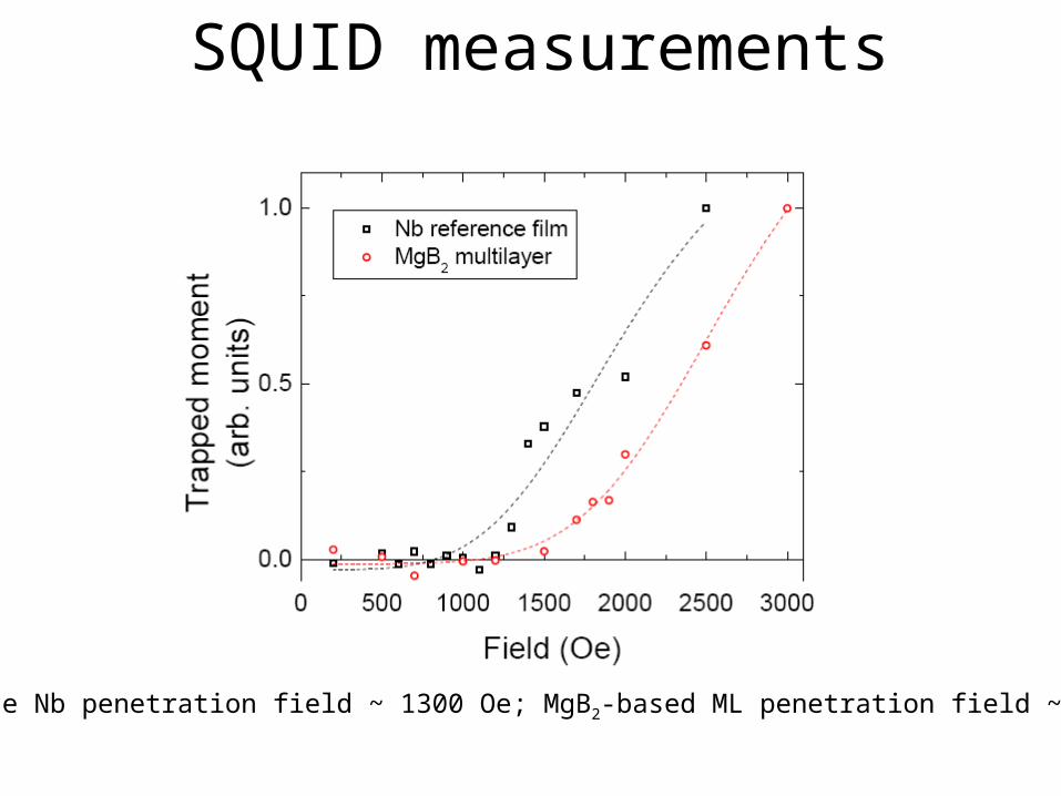
SQUID measurements
Reference Nb penetration field ~ 1300 Oe; MgB2-based ML penetration field ~ 1700 Oe

Surface impedance characterizations (SIC)
• The ultimate performance test of the films and multilayers for this application is a measurement of their surface impedance, Rs.
• We note that Rs can be written as:Rs = RBCS (T) + Ri,
where RBCS = (Aw2/T) exp[-D/(kBT)]
Note: Rs decreases strongly for higher-Tc materials with larger superconducting gap Δ = 1.86Tc, implying that materials with Tc > 20K, could have the RBCS at 4.2 K comparable to RBCS of Nb at 2K. However, small Rs also implies small residual resistance Ri and no nodes in the superconducting gap, which rules out the d-wave high-Tc cuprates for which Rs T∝ 2
• JLab’s SIC system is uniquely capable of making temperature-dependent RF surface impedance measurements on 2inch-sized thin film samples.
• Summary of 2 inch samples studied:
o Nb thin films grown under various conditions
o Epitaxial MgB2 filmso NbN-based trilayer on coppero NbTiN-based multilayers deposited
on sapphire

Nb thin films grown under different conditions
Nb films were grown atJlab at different T, and bias conditions, etc. using ECR

MgB2 films epitaxially grown on sapphire

At the SRF 2011 the surface impedance of a MgB2-based multilayer was reported, and the residual resistance was found ~ 181 mW

Samples grown on Cu substrates contained large grains (on the order of millimeters) that were visible to the naked eye. The surfaces of these samples are dominated by rough features as seen with SEM and optical microscopy. After annealing 10 nm of MgO and 60 nm of NbN were deposited (W&M).
NbN-based ML Samples deposited on Cu substrates

SIC for NbN/MgO/Nb trilayer on Copper
We note that the residual resistance (Ri) around 2K is approximately 35 mOhm.

2 3 4 5 61
10
100
1000
10000 NbN/MgO/Nb/Cu Nb/Cu-ECR70-360°C/360°C, -180V(7')+0V(23') Nb/Cu-ECR64-360C/360C, -180V (30') Large grain Niobium
RS()
T(K)
SIC comparison
We notice that the residual resistance of these thin film samples is one order larger thanthat of bulk Nb around 2K but in general lower than that of MgB2-based ML samples.

Cu
NbTiNAlN
Nb
NbTiN
AlN NbTiN
N2/Ar 0.33 0.23
Total pressure [Torr] 2x10⁻³ 2x10⁻³
Sputtering Power [W] 100 300
Deposition rate [nm/min] ~ 5 ~ 18
Thickness [nm] 10 100
Tc [K] N/A 14
NbTiN-based SIS structures on bulk Nb and Nb/Cu substrates
NbN-based multilayers have been very promising regarding magnetic shielding, but we notethat this material suffers from a higher resistivity due to the presence of both metallic and gaseous vacancies randomly distributed while the ternary nitride NbTiN presents all the advantages of NbN and also exhibits increased metallic electrical conduction properties with higher titanium (Ti) percentage.
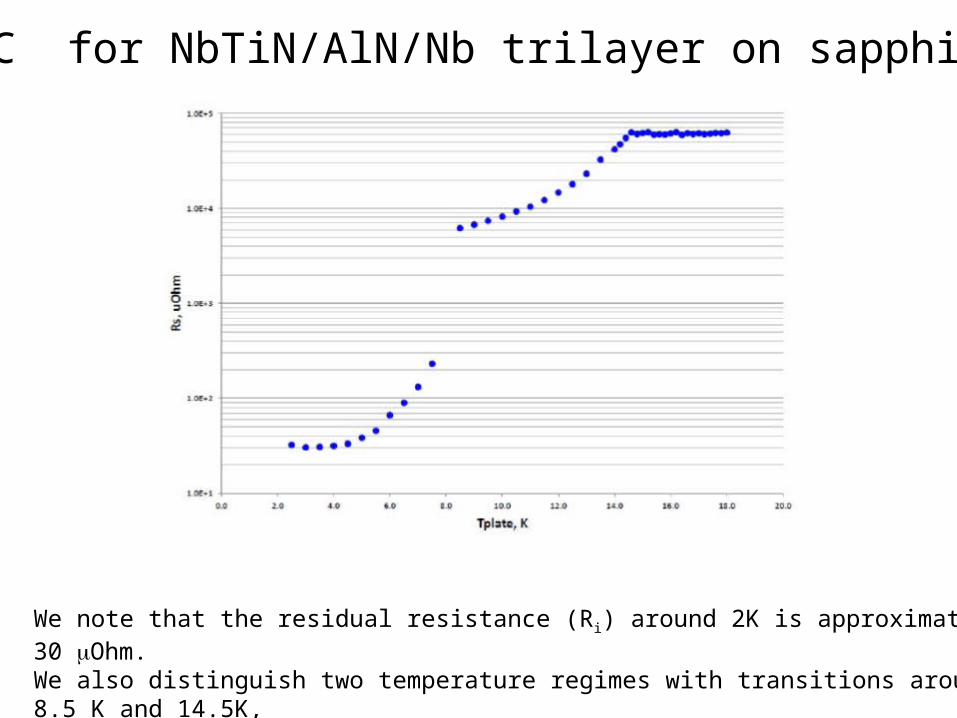
We note that the residual resistance (Ri) around 2K is approximately 30 mOhm. We also distinguish two temperature regimes with transitions around 8.5 K and 14.5K, related to Nb and NbTiN respectively.
SIC for NbTiN/AlN/Nb trilayer on sapphire

Conclusions• Multilayers incorporating NbN and following the “Gurevich
model” were shown to shield niobium in the pioneer work by Antoine et al. using SQUID magnetometry as well as third harmonic analysis.
• By tailoring thin film growth parameters, our own work also using SQUID magnetometry was able to demonstrate shielding beyond the critical field of Nb also using NbN-based trilayers.
• We have demonstrated that other suitable superconductors also show promise for SRF applications, but further studies to optimize thin film deposition conditions must be undertaken in this case.
• This work is supported by the Defense Threat Reduction Agency (DTRA) under grant # HDTRA1-20- 1-0072.