Embed Size (px)
Citation preview

10kV/30kA Unipolar Arbitrary Voltage Source for Hardwarein- the-Loop Simulation Systems for HVDC Circuit Breakers
C. Carstensen and J. Biela
Laboratory for High Power Electronic Systems ETH Zurich, Physikstrasse 3, CH-8092 Zurich, Switzerland
Email: [email protected], URL: http://www.hpe.ee.ethz.ch
„This material is posted here with permission of the IEEE. Such permission of the IEEE does not in any way imply IEEE endorsement of any of ETH Zürich’s products or services. Internal or personal use of this material is permitted. However, permission to reprint/republish this material for advertising or promo-tional purposes or for creating new collective works for resale or redistribution must be obtained from the IEEE by writing to [email protected]. By choosing to view this document you agree to all provisions of the copyright laws protecting it.”

10kV/30kA Unipolar Arbitrary Voltage Source for Hardware-in-the-Loop Simulation Systems for HVDC Circuit Breakers
C. Carstensen and J. BielaLaboratory for High Power Electronic Systems
ETH Zurich, Physikstrasse 3, CH-8092 Zurich, SwitzerlandEmail: [email protected], URL: http://www.hpe.ee.ethz.ch
KeywordsMultilevel Converters, HVDC, HV Power Converters, Pulsed Power Converter, Interleaved Converters, ZVS Converters
AbstractIn this paper a novel topology for an unipolar arbitrary voltage source for high power Hardware-in-the-Loop SimulationSystems is presented. The maximal output voltage is 10 kV and a maximal output current of 30 kA can be providedfor a duration of 20 ms with a maximal current gradient of 200 A/µs. The system enables in-depth research and futuredevelopments of circuit breakers for future multi-point DC transmission systems.
1 IntroductionThe change from centralised conventional electrical power generation to distributed and fluctuating renewable energysources requires a change in power transmission and distribution system technology. Currently existing AC grids reachtheir limits when dealing with these new power sources, necessitating more high voltage DC transmission systems (HVDC)in the future. This could finally be enhanced to a HVDC super grid (see e.g. DESERTEC project, [1]).
In multi-point DC transmission systems, new circuit breaker concepts are required for isolating faulty grid parts in caseof a failure. Thus far, switches for AC grids, which are enhanced to handle DC currents of up to 4 kA [2, 3, 4] are utilisedfor this task. However, research on DC grids has shown, that much higher failure currents (up to 30 kA) have to be expected,so that further investigations on new DC circuit breaker concepts are required [5].
For investigating / testing DC circuit breakers two different kinds of energy sources have been used up to now. Duringthe tests a current pulse with a high peak amplitude is flowing through the circuit breakers simulating a short circuit.Simple test setups use a capacitor for energy storage and connect the capacitor through a switch to a serial combination ofan inductance and a resistor to provide a smooth current, which is then interrupted by the analysed circuit breaker [6]. Thisis a very simple solution, which is easy to control, but the drawback is a limited influence on the current/voltage waveformsexcept by changing the circuit elements.
More advanced setups use power electronic converters to provide a high current at low voltage. This simulates theconduction time of the circuit breaker during a fault situation. The high voltage, which occurs while interrupting thecurrent, is generated by a spark gap that is triggered to connect a pre-charged capacitor parallel to the circuit breaker[7, 8, 9]. This is called synthetic test setup and is a typical approach in high voltage engineering because no high powersupply is needed. However, based on this setup the current and voltage cannot arbitrarily be shaped in order to investigatethe circuit breaker during the turn-off process in detail.
Device under testHVDC Circuit Breaker
LF
CF
VC
Modular Multi Level Marx Type ConverterM³TC
based on Half-Bridge Submodules
- Staircase Voltage -
PolaritySwitch
3-Level Converter
Charging Unit 1
VO2
VO1
VArc
VStVout
- Linear Voltage -
Charging Unit 2
Figure 1: Basic concept of the proposed Unipolar Arbitrary Voltage Source(UnAVoSo) consisting of 21 parallel sources, which each is a combination of astair case voltage source (M3TC) and a low voltage linear source.
Table I: Specifications of the Unipolar ArbitraryVoltage Source (UnAVoSo).
Output voltage Vout 10 kV
Output current Iout 30 kA
Max. current gradient di /dt |max 200 A/µs
Operation period TPulse 20 ms
Charging period 5 min

The latest research uses a buck converter to create arbitrary current/voltage waveforms [5] . A small buck inductanceenables high current rise rates and the possibility to simulate the behaviour of a HVDC grid during fault conditions. Thus,this setup combines the good controllability of a synthetic test setup and the realistic conditions of the capacitor based so-lution. However, the switching losses of the semiconductor restricts the operation to several hundred switching transitions,limiting the maximum current amplitude and current shaping possibilities.
In order to overcome these limitations, a novel concept for an advanced Unipolar Arbitrary Voltage Source (UnAVoSo)for a Hardware-in-the-Loop Simulation System (HiLSS) as shown in Fig. 1 is presented in this paper. Based on previousstudies on circuit breakers and faults in HVDC transmission systems, the maximal output voltage of the new system is setto 10 kV, with the system able to provide output currents of up to 30 kA for a period of up to 20 ms (cf. Table I). Duringthe turn-off process of the circuit breaker, high transient voltages and currents can occur, and as a result the system mustbe able to generate signals with a current rise rate of up to 200 A/µs. A typical current shape of UnAVoSo is depicted inFig. 15e).
The energy required during one turn-off process of the circuit breaker is provided by capacitors in order to avoiddisturbances of the supplying grid. In the HiLSS the current through the circuit breaker is measured and the voltage acrossthe inductance LF is adjusted so that a predefined current flows. However, it is also possible to control the voltage shapeVArc. After each turn-off action, the energy storage capacitors can be recharged during 5 minutes.
In section 2, a detailed description of the operating principle of the unipolar arbitrary voltage source is given. The twosubsystems of the converter – the voltage submodules and the 3-level converter – are investigated in section 3 and 4. Thecontrol of the system is described in section 5 and the results are shown in section 6 by simulation models, and finally aprototype system is discussed in section 7.
2 Operating PrincipleConsidering the challenging specifications listed in Table I, conventional linear amplifier concepts and also hybrid conceptsbased on a switch-mode power supply combined with a linear amplifier as presented in [10], cannot be applied to generatethe required voltage/current. This approach would result in high conduction/switching losses that would prevent highefficiency due to the high operating voltage/current. Therefore, in [5] a buck converter is used, which applies 4.5 kV IGBTsto generate a single 3 kV arbitrary shape voltage pulse. For increasing the output voltage to 10 kV a series connection ofIGBTs would be necessary. However, even in the basic 3 kV source the switching losses are too high, so that only a limitednumber of switching transitions can be performed before the junction temperature hits the thermal limit.
Therefore, the presented arbitrary voltage source is based on a series connection of half bridge-submodules (Fig. 3,Modular Multi-Level Marx-Type Converter, M3TC) generating a staircase output voltage VO1 as shown in Fig. 2d withvoltage steps VSt = 1.1kV. In order to fill up the gaps between the voltage steps and generate a smooth output voltage,continuous voltage source is connected in series to the staircase voltage generator. Based on this approach the operatingvoltage of the continuous voltage source is significantly reduced, so that fast switching IGBTs can be used. This incombination with the lower operation voltage results in drastically lower switching losses and boosts the efficiency. Becauseof the large output currents, the converter system is split up into 21 parallel connected modules, that each provides a currentof up to 1.4 kA.
The detailed operating principle can be seen in Fig. 2, where the generation of a linearly rising output voltage VOut(Fig. 2e) is shown. Starting at VOut = 0V (t = t1), all submodules are turned off, i.e. VO1 = 0V and the continuous voltage
t2t1 t3
e)
VOut
t0
1
2
3
4VSt
t2t1 t3
b)
0
1
-1
Sign
t
VO1VSt
d) 0
1
2
3
4
t
a) 0
0.5
VC
t
VSt
0
-0.5
0.5
c)
VSt
VO2
tX
- Continuous Source -
- Staircase Source -
Figure 2: Output voltages of the different converter sys-tems related to the step voltage VSt : a) Output voltage VO1of the 3-level inverter, b) sign of the Polarity Change Unit,c) output voltage VO2 of the Polarity Change Unit, d) out-put voltage of M3TC and e) total system output voltageVOut .
SC n
SC 1
Sd n
Sd 1
Cn
VO1
VSt
IO1
C1
VC1
D1Marx Type Converter Cell
- Submodule -
Charging Unit
DCPFCRectifier
DC
VCn
Figure 3: Modular Multi-Level Marx-Type Converter (M3TC) withcharging circuit for capacitors Cn.
source generates a linearly rising output voltage VC. This voltage is connected via the Polarity Change Unit with a positivesign to VO2. As soon as VO2 is VSt
2 = 550V (t = t2), the first submodule is turned on, so that VO1 =VSt = 1.1kV. At the sametime the polarity of VO2 is changed from +550 V to -550 V (Fig. 2b and c), so that the sum of the two voltages VO1 and VO2is equal to 550 V. Then, because of the negative sign of the Polarity Changer, the amplitude of VO2 is linearly decreased to0 V, so that the sum VO1 +VO2 increases to 1.1 kV. When VO2 becomes 0 V (t = t3), the polarity of VO2 is changed again andVO2 rises with VC again.
Consequently, for a linear rising voltage, VC has to be a triangle voltage, which in the considered case of VOut,max = 10kVhas to have a nine times (VOut,max
VSt= 9) higher frequency than VOut and an amplitude of VSt
2 (Fig. 2a). The Polarity Changerperforms a periodic sign change (Fig. 2b), so a saw tooth signal with an amplitude between -550 V and +550 V is generated(Fig. 2c).
3 Modular Multi-Level Marx-type ConverterThe M3TC is a combination of a modular multi-level (M2C) converter ([11], [12]) and the charging concept applied inMarx generators. The M3TC consists of nine stages, that each could provide a voltage of 1.1 kV (Fig. 3). A stage consistsof a capacitor Cn for energy storage, two IGBTs SCn/Sdn and a charging diode. By turning on IGBT SCn, capacitor Cn isconnected in series to the main circuit so that VCn = 1.1kV is added to VO2. In case SCn is turned off, current IO1 flowsthrough the free-wheeling diode of Sdn and the stage adds≈ 0 V to VO2. Each stage can be turned on/off separately allowingthe output voltage to change in 1.1 kV increments.
As a result of this topology the used IGBTs have to perform less than ten switching actions during one pulse in theoperation period TPulse (c.f. Fig. 15e). Thus they can be chosen with a low forward voltage drop in the on-state.
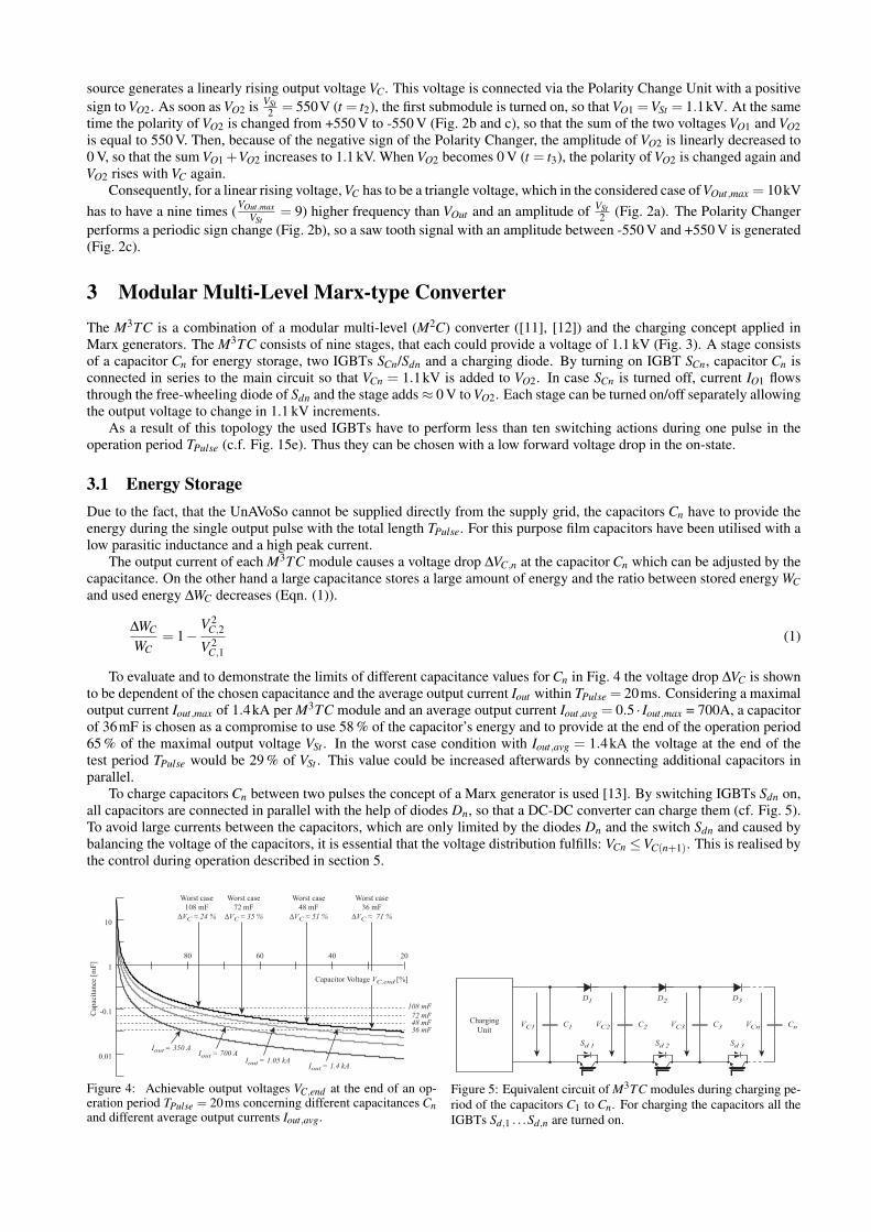
3.1 Energy StorageDue to the fact, that the UnAVoSo cannot be supplied directly from the supply grid, the capacitors Cn have to provide theenergy during the single output pulse with the total length TPulse. For this purpose film capacitors have been utilised with alow parasitic inductance and a high peak current.
The output current of each M3TC module causes a voltage drop ∆VC,n at the capacitor Cn which can be adjusted by thecapacitance. On the other hand a large capacitance stores a large amount of energy and the ratio between stored energy WCand used energy ∆WC decreases (Eqn. (1)).
∆WC
WC= 1−
V 2C,2
V 2C,1
(1)
To evaluate and to demonstrate the limits of different capacitance values for Cn in Fig. 4 the voltage drop ∆VC is shownto be dependent of the chosen capacitance and the average output current Iout within TPulse = 20ms. Considering a maximaloutput current Iout,max of 1.4kA per M3TC module and an average output current Iout,avg = 0.5 · Iout,max = 700A, a capacitorof 36mF is chosen as a compromise to use 58 % of the capacitor’s energy and to provide at the end of the operation period65 % of the maximal output voltage VSt . In the worst case condition with Iout,avg = 1.4kA the voltage at the end of thetest period TPulse would be 29 % of VSt . This value could be increased afterwards by connecting additional capacitors inparallel.
To charge capacitors Cn between two pulses the concept of a Marx generator is used [13]. By switching IGBTs Sdn on,all capacitors are connected in parallel with the help of diodes Dn, so that a DC-DC converter can charge them (cf. Fig. 5).To avoid large currents between the capacitors, which are only limited by the diodes Dn and the switch Sdn and caused bybalancing the voltage of the capacitors, it is essential that the voltage distribution fulfills: VCn ≤VC(n+1). This is realised bythe control during operation described in section 5.
Worst case108 mF
∆VC ≈ 24 %
Worst case72 mF
∆VC ≈ 35 %
Worst case48 mF
∆VC ≈ 51 %
Worst case36 mF
∆VC ≈ 71 %
Iout = 1.4 kA Iout = 1.05 kA
Iout = 700 A Iout = 350 A
Capacitor Voltage VC,end [%]
Cap
acita
nce
[mF]
108 mF72 mF48 mF36 mF
80 60 40 20
0.01
-0.1
1
10
Figure 4: Achievable output voltages VC,end at the end of an op-eration period TPulse = 20ms concerning different capacitances Cnand different average output currents Iout,avg.
Sd 1 Sd 2 Sd 3
ChargingUnit
C1
D1 D2 D3
VC1 C2 C3 CnVC2 VC3 VCn
Figure 5: Equivalent circuit of M3TC modules during charging pe-riod of the capacitors C1 to Cn. For charging the capacitors all theIGBTs Sd,1 . . .Sd,n are turned on.

4 3-Level Inverter & Polarity Change UnitThe continuous voltage source (Fig. 6) consists of an asymmetrical 3-level inverter and a H-bridge circuit for polaritychanging. As shown in Fig. 6 the capacitor Cout is charged respectively discharged by six interleaved 3-level inverterswhich are coupled by using separate output inductors (L1, ...,L6). The Polarity Change Unit (PCU) connects this capacitorCout with positive (using switches SPS,1 and SPS,4) or negative (using switches SPS,2 and SPS,3) polarity to VO2.
Due to the voltage adding concept as presented in section 2 the continuous voltage source requires a high output signalfrequency and a high slew rate. This can be achieved by using a high switching frequency, but with the disadvantage oflarge switching losses. To solve this, the converter uses zero-voltage-switching (ZVS) to reduce the switching losses andinterleaving to reduce the current ripple.
An asymmetrical 3-level inverter is chosen because only positive voltages VC must be generated. To enable fast switch-ing IGBTs with VCE,max = 600V are chosen, so that with an operating voltage range of 400 V per IGBT an output voltagerange of 800V of the 3-level inverter results. To control the inductor current IL, it is necessary to apply positive and neg-ative voltages VL. Considering the range of VC from 0 V to 550 V the 3 output levels are chosen as V3L,neg = −125V,V3L,MP = 275V and V3L,pos = 675V = 550V+125V. Thus it is possible to apply at least VL =±125V across the inductor.
To enable ZVS it is necessary to use a discontinuous current mode (DCM) to generate both a positive and a negativecurrent during a switching cycle (cf. Fig. 10 and [14]). Therefore, the output inductance of the 3-level inverter has to bechosen to provide fast current gradients.
Concerning the maximal output current of a M3TC module with Iout,max = 1.4kA, a projected switching frequencyof f3L,period = 10kHz and a minimal voltage across Ltotal of VL = 125V, which is caused by the difference between themaximal output capacitor voltage VC,max = 550V and the maximal positive voltage V3L,pos, the value of Ltotal can becalculated. Ltotal represents the inductance of the 3-level inverter, if the system is realised without interleaving and onlyone 3-level inverter (c.f. section 5).
dIL = 2 · Iout,max + IC,change = 3kA dt =1
f3L,period= 100µs
VL =VC,max−V3L,pos = 150V Ltotal = 5µH (2)
Because of using 6 interleaved inverter, the output current has to be divided equally to all inverters. By choosingLn = 6 ·Ltotal the maximal current gradients are reduced to 1/6 and the output current is also reduced by a factor of six. Thechoice of parameter for a 3-level inverter is listed in Table II.
L1
IL,1 Polarity Change Unit
3-Level Converter
CoutVC
0 .. 550 VVO2
S3L, 1
SPS, 1
SPS, 3
SPS, 2
SPS, 4
S3L, 2
CS5
CS1
CS2
CS3
CS4
S3L, 3
S3L, 4
C3L, 1
C3L, 2
C3L, 3
MP
C3L, 4
D3L, 1
D3L, 2
200 V
200 V
275 V
125 V
IL,2
IL,3
IL,4
IL,5
IL,6
VL
Figure 6: 6 times interleaved 3-level inverter with Polarity Change Unit(PCU) for generating a continuous arbitrary voltage VO2.
Table II: Components of the 3-level inverter.
Name Value Condition
C3L,1, ... , C3L,4 53mF -
CS1, ... , CS4 40nF VCSn = 200V
CS5 1µF VCS5 = 200V
Cout 600µF Vout = 550V
L1, ... , L6 30µH VL = 800V
5 Control of UnAVoSoThe control of UnAVoSo, depicted in Fig. 7, consists of a controller part, a stage selector, the M3TC stages, 3-level inverterplus Polarity Change Unit (PCU) and the main output inductor.
The controller (1) is consists of three elements: To compensate the error between the reference value Ire f and thereal output current Iout a PI controller is utilised. To improve the response time of the system for current gradients a PDcontroller is additionally used as pre control to deviate the reference value. Thus a gradient of Iout,re f generates immediatelya voltage step of Vout,re f . The third part of the controller adds the arc voltage VArc to Vout,re f as a pre control to avoid largechanges of the output current Iout affected by a change of load voltage VArc.

M3TCstageselect
M3TC
measuredVC1 , ... , VC9
Switching States of M3TC
Output Inductance
Xsignum
abs
Stage ControllerController1
Inverter
Error Compensation
Pre Control
Polarity Switch Unit
Iref
VArcVArc, pre
Idiff
Iout
Vout, ref
VO1
VSum
VC, ref VC
VO2
Vout
VL
VArc
Polarity(± 1)
Vcontrol
Vpre
9
-
-
-
2 3
3-levelinverter
Figure 7: Control of UnAVoSo consisting of a controller part, a stage selector to convert the reference value Vout,re f to switch states ofM3TC and PCU and VC,re f for the 3-level inverter.
5.1 Model of the 3-Level InverterThe use of a variable length of the switching period Tperiod in combination with interleaving the six 3-level inverters requiresthe prediction of the output currents ILn and voltage VC for a whole period in advance to allow the synchronisation of theinverters. Thus the control of the 3-level inverter system is based on a mathematical model of an inverter module, which isapproximated using Taylor series expansion.
To identify the model’s description the equivalent circuit shown in Fig. 9 is used based on a voltage source V3L describingthe inverter output voltage VCon, the total inductance and a constant output current Iout,0. Because of the relatively largemain inductance LF and the switching period Tperiod ≈ 100µs this current can be assumed constant.
VL = LtotaldIL
dtIC =Cout
dVC
dt(3)
VL =VCon−VC IL = IC + Iout (4)
Differential Eqn. (3) and Eqn. (4) have been combined and solved by using initial values IL = IL,0 and VC = VC,0 att = 0 (Eqn. (5)).
IL(t) =
√Cout
Ltotalsin( t√
LtotalCout
)(VCon−VC,0
)+ cos
( t√LtotalCout
)(IL,0− Iout,0
)+ Iout,0 (5)
The stage selector (2) converts the continuous voltage signalVout,re f to switching states of the M3TC and the PCU and cal-culates a reference signal for the 3-level inverter system. Thedetailed stage selection of M3TC is shown in Fig. 8. In thebeginning of the calculation all M3TC stages are assumedto be switched off, so the output voltage VO1 = Vsum = 0V.Based on the measured capacitor voltages VCn of M3TC,there is a comparison, if the difference between the refer-ence value Vout,re f and the voltage Vsum, which representsthe voltage of the turned on M3TC stages, is larger than halfthe capacitor voltage VCn. If this statement is false, it is pos-sible to generate this difference by using the 3-level inverter.Otherwise an additional stage has to be turned on and thatvoltage VCi is added to Vsum. At the end of a calculation cy-cle there is a delay of 50 µs to avoid fast oscillations. Byalways starting with the first M3TC stage to be turned on, itis secured, that the condition for recharging VCn ≤VC(n+1) isfulfilled at every time.Corresponding to Fig. 2 the sign of the difference betweenVO1 = Vsum and Vout,re f is used to control the state of thePolarity Switch Unit, while the reference signal VC,re f forthe 3-level inverter is the absolute value of this difference.The 3-level inverter includes an additional control and mod-ulation part, which is depicted in Fig. 13 and will be de-scribed in the following subsections.
yes
no
Delay 50 µs
Store the MT3C switching state as ON
Set new MT3C switching states
( Vout, ref - Vsum ) > 0.5 · VC, i
Vsum = Vsum + VC,i
Vsum = 0
i = i + 1
i = 0
Start
Initialise
Figure 8: Algorithm to convert the voltage control signal Vout toswitching states of M3TC and of the Polarity Switch and calculatethe value VC,target for the 3-Level Inverter System.

VConV3L VC Iout,0Cout
Ltotal IL Iout
IC+-
Figure 9: Equivalent circuit diagram of the combined 3-level in-verter with inverter output voltage VCon, inductance Ltotal =
16 Li,
capacitor Cout and the output current Iout,0, which is assumed to beconstant.
S23
Tperiod
S2 S3
State S1 State S2
Time t
State S3 State S5
State S4tS4 = 0
Inductor Current IL
IPeak
V3L = V3L, pos V3L = V3L, posV3L = V3L, MP V3L = V3L, neg
(1 - k) IPeak
(1 + k) IPeak
-IL,min
Figure 10: Inductor current IL with a positive Ipeak value usingDCM to provide ZVS with VC > V3L,MP because of reaching IL =(1− k)IPeak at the end of state S2.
To achieve a high dynamic, capacitor Cout is chosen to be as small as possible. Thus a voltage ripple ∆VC is expecteddue to the non constant current IC (Eqn (6)).
VC(t) =VCon−LtotaldIL
dt(6)
To realise the calculation in a digital controller system, the equations are approximated by a Taylor series expansion.The current IL is approximated by a 3rd degree Talor polynomial and the voltage VC by a 2nd degree polynomial.
5.2 Modulation of the Master 3-Level InverterTo enable interleaving the modulation of the 3-level inverter system is divided into a master inverter and 5 slave inverters,which are synchronised and time shifted to the master.
To provide ZVS it is necessary to use a discontinuous current mode (DCM) and generate at each switching period botha positive and a negative inductor current IL with an amplitude of at least IL,min (see Fig. 10). This is necessary to dischargethe capacitors CSn before turning on the IGBTs. The peak current IPeak is used as control variable.
DCM is realised by a state machine, depicted in Fig. 11, that can generate both positive and negative current peakvalues. For positive peak currents IPeak state S1 is used to generate this current by using V3L =V3L,pos. S2 uses V3L =V3L,MPand IL will reach for V3L,neu >VC the upper respectively for V3L,neu <VC the lower limit of a range defined around IPeak bythe factor k. The following state S3 is used to generate a negative current peak with an amplitude of −IL,min. State S4 is notused with positive peak currents. The last state S5 uses V3L =V3L,pos and decreases the negative current IL to zero.
Switching DelaySwitching Delay
Switching Delay Switching Delay
( IL ≥ IPeak ) and (IL ≥ IL, min)
Intial State for Slave ConvertersAll IGBTs turned off
IL = 0
( IL ≤ IPeak ) and
(IL ≤ -IL, min)
( IL ≥ (1 + k) IPeak ) or ( IL ≤ (1 - k) IPeak )
( IL ≥ (1 + k) IPeak ) or ( IL ≤ (1 - k) IPeak )
V3L = V3L, pos
V3L = V3L, MP
V3L = V3L, MP
V3L = V3L, neg
V3L = V3L, pos
State S1
State S0
State S12
State S2
State S23
State S3 State S34
State S4
State S45
State S5
Figure 11: State machine to control the interleaved, ZVS, fre-quency variable 3-Level inverter System including the start stateS0.
a) b)t2
MasterSlave
∆tn ∆tn ∆tnT
Inductor current IL
Time t
∆t ∆tet1
Proposed Slave
Master
Real Slave
Figure 12: Interleaving and synchronisation of the 3-level inverterwith a) adjusted offset of ∆tn and b) error calculation ∆te.

Error Compensation
Pre ControlTime
Calculation
Time controlled
Time controlled
Time controlled
Adaptingswitching
timesSlave
Master
StateMachine
StateMachine
9 4
-
-
-
V3L,1 VL1 I3L,1 IL, total
Switching States
IC
Iout,0
VCVC
VC, ref
VC, diff
IPre
IControl
IPeaktsn
49
VC
3 LevelInverter
3 LevelInverter
-
V3L,2 VL2 I3L,2
Inductor L2
Inductor L1 Capacitor Cout
VC
Adaptingswitching
timesSlave
StateMachine
49
3 LevelInverter -
V3L,3 VL3 I3L,3
Inductor L3VC
Polarity
Figure 13: Control of the 3-level inverter system consisting of a PI- and a PD-controller, a module to calculate the times for the differentstates, a master inverter system and 5 slave inverter systems.
For negative peak currents, caused by a negative polarity of the PCU, the states S1 and S3 are used to generate thecurrent ripple of +IL,min for ZVS, while state S4 is used instead of S2. States S12, ...,S45 are for the interlock delay.
For achieving interleaving, at beginning of state S1, a whole cycle of the state machine is calculated in advance basedon the mathematical model. For this purpose the Talyor approximation of Eqn. (5) has been transformed to calculatethe time tSn, that is needed to reach a certain current IL(tSi), based on the initial conditions at the beginning of each state(VC,0 = VC,S(i−1), IL,0 = IL,S(i−1), VCon, Iout,0). By using the time tSi and the approximated equations of (5) and (6), IL,Siand VC,Si at the end of the state are calculated. This is done for all states (i = 1, ...,5), so that the time of the period isapproximately Tperiod = ∑ tSi +4 · tInterlock.
The master 3-level inverter is controlled by these calculated times. To compensate current offset errors at the end of aperiod (i.e. IL(Tperiod) 6= 0), the time tS5 is recalculated at entering state S5 using real measurements as initial conditionsIL,0 and VC,0.
5.3 Modulation of the Slave 3-Level InvertersEach of the five interleaved converter has its own time-based state machine SMS, j ( j = 1, ...,5) and as soon as they enterstate S1 the switching times are copied from the time calculation unit (cf. Fig. 13). For interleaving it is necessary, that thebeginning of a cycle of the slave state machines j is time shifted to the beginning of the master cycle by
∆t = j ·∆tn =jn
TPeriod . (7)
To adjust the time offset between the single inverters for a positive peak current Ipeak, the time tS2 of state S2 is addi-tionally recalculated by using Eqn. (8) (see Fig. 12).
tS2,new = tS2−∆te = tS2− (t2− t1−∆t) = tS2− (t2− t1−jn
Tperiod) (8)
Because of changing the time for S2 an current offset error is generated. This error is compensated by adapting thetimes for state S3. Using the new times tS2,new, IL(tS2,new) and VC(tS2,new) are recalculated and based on this new initialconditions, the time tS3 is computed.
For negative peak currents the times for the states S4 and S5 are used in the same way to synchronise interleaving.The complete control of the 3-level inverter system is depicted in Fig. 13. The reference value Ipeak for the modulation
part is generated by a PI controller for error compensation and a PD controller to improve the step response time.By changing the state of the PCU the sign of the output current Iout,0 is inverted. In order to enable a fast response
to this large current gradient, the polarity signal is monitored. As soon as the polarity is switched, the times tSn of bothmaster and slave state machines, beginning with the current state, are recalculated. Due to this interruption of the normalmodulation process, interleaving is disturbed and has to be synchronised again.
6 Simulation ResultsFor designing the system and evaluating the performance, the proposed system has been modelled in detail in GeckoCircuitT M .There, also the thermal design of the system considering switching and conduction losses is included in the simulationmodel.
The simulation results of the prototype system, which is described in section 7, are shown in Fig. 15. A typical currentwave form (see Fig. 15e) consists of an arc ignition period (1) between 0ms and 10ms, a constant current (3) between12ms and 22ms and typically a fast current gradient (4) at 22ms to 22.07ms to the peak current.

3-Level-Inverter
36 mF Film Capacitor889 mm
1330 mm
2882 mm
M3TC Stage
Polarity Change Unit
Figure 14: 3D Model of one UnAVoSo module, including nineM3TC stages, six 3-Level Inverters including supply capacitorsin the bottom part and in between the Polarity Change Unit.
Pulse Duration 50 µs
Vout
Vout, ref
Iout
TPulse
Iref
b)
a)
c)
d)
e)
Num
ber o
f tur
ned-
on
M3
TC m
odul
esSt
ate
of
Pola
rity
Switc
hVo
ltage
VC
[V]
Volta
ge V
ou
t [V]
Cur
rent
I ou
t [A]
Time t [ms]
Time t [ms]
Time t [ms]
Time t [ms]
Time t [ms]
0 10 20 30 40
0123456
-1
0
1
0
100
200
300
400
500
600
0
1000
2000
3000
4000
5000
0
300
600
900
1200
15000 10 20 30 40
0 10 20 30 40
0 10 20 30 40
0 10 20 30 40
1 2 3 4 5 6
Figure 15: Simulation result of the prototype system generatinga typical current shape, showing (a) the numbers of switched onM3TC modules, (b) the state of the Polarity Change Unit, (c) theoutput voltage VC of the 3-Level Inverter System, (d) the voltagecontrol signal Vout and the real output voltage VUnAVoSo and (e) thetarget current signal Itarget and the real output current Iout .
During the arc ignition (1) the current Iout is controlled only by the 3-level inverter system due to low arc voltage andlow current. By adjusting the arc, the current is increased to a constant current (2), using the combination of M3TC, PCUand 3-level inverter system (see Fig. 15a), b) and c). During period (3) the voltage drop ∆VCn of the M3TC stages has to becompensated by increasing the voltage VC of the continuous source. The fast current gradient (4) is mainly generated byswitching two additional M3TC stages, while the 3-level inverters system remains almost at the same output level.
Period (5) provides again a constant current Iout = Iout,max, causing a voltage drop ∆VCn and this has to be compensatedby adding more M3TC stages.
The more detailed simulation result of the 3-level inverter system, shown in Fig. 16, presents a triangle output voltageVC with an amplitude of 550V and a constant output current Iout,0 = 800A which polarity must be changed when thegradient of VC,re f changes. The ripple of the output current ∑ IL,n after switching Iout,0, shows, that the inverter control hasto synchronise the interleaving again. Furthermore, the adaptation of the inverter output current requires approximately100µs which causes a voltage ripple on the output voltage VC, which will be reduced by optimising the controller in thenext steps.
In Fig. 17 the synchronised interleaving of the 3-level inverter is shown. The currents of the separate inverters aredistributed equally (Fig. 17b) and adjusted in every single cycle by readjusting the switching times (Fig. 17a). Due tointerleaving, the ripple of the total output current is very small and the voltage ripple on VC (Fig. 17c) is minimised. Furtherthe output voltage VCon,1 of one inverter (Fig. 17c) rises relatively slow during switching due to ZVS conditions.

Iout, 0
∑ ILn
IPeak
VC, refVC
Indu
ctor
cur
rent
s [A
]Vo
ltage
VC
To
tal c
urre
nts [
A]
-600
-400
-200
0
200
400
600
800
-3000
-2000
-1000
0
1000
2000
3000
-110
0
110
220
330
440
550
5 7.5 102.50
5 7.5 102.5
5 7.5 102.5
Time t [ms]
Time t [ms]
Time t [ms]
a)
b)
c)Figure 16: Simulation result of the 3-level inverter system, show-ing (a) the six interleaved inductor currents ILn, (b) the sum of thesecurrents and the for control purposes used peak current value IPeakand (c) the reference voltage VC,re f and the real capacitor voltageVC for an output current Iout,0 = 800A.
VCon, 1
a)
b)
c) Time t [µs]
Time t [µs]
Time t [µs]
Adjustment of the times
Slow voltage risedue to ZVS
VC
1 2 3 4 5 6
IL1
0 100 150 200
IL2 IL3 IL4 IL5 IL6
Stat
es o
f the
diff
eren
t inv
erte
rsIn
duct
or c
urre
nts [
A]
Volta
ge [V
]
0
2
4
6
8
10
-50
0
50
100
150
200
250
300
350
-200
0
200
400
600
800
50
100 150 200 50
100 150 200 50
Figure 17: Simulation results of the interleaved 3-Level InverterSystem, showing (a) the states of the six state machines, (b) theinductor currents ILn and (c) the capacitor voltage VC and the in-verter output voltage VCon,1 including slow rising gradients causedby ZVS.
7 Prototype SystemBased on the simulation results a prototype system of one module (Iout,max = 1.4kA, Vout,max = 10kV) has been designed.The main components and the required number of devices are listed in Table III. To minimise overvoltages the parasiticinductance has been reduced by using integrated 3-level switches as well as wide copper bus bars.
The main limitation for generating high dynamic current gradients by switching at high frequencies is the junctiontemperature, so that the switching losses must be reduced and the thermal design of the system is crucial. Based on thesimulation, described in section 6, the thermal losses of the semiconductors have been estimated (see Fig. 19). Due to pulseoperation and the thermal capacitances, the losses could exceed the loss values given for steady state operation.
IL(tS3) IL(tS4) IL(tS5)
IL(tS2)
IL
IL(tS1)
Time [µs]
Indu
ctor
cur
rent
[A]
State S1 State S2 State S3 State S5
0 20 40 60 80 100 120
-50
0
50
100
150
200
250
Figure 18: Validation of the model by simulation results, show-ing the inductor current ILn during one switching period and theestimated currents at the end of the different states IS1, ..., IS5.
S3L, 1 S3L, D1 S3L, 2 S3L, D2 S3L, 3 S3L, D3 S3L, 4 S3L, D4 D3L, 1 D3L, 2
M3TC Modules
Polarity Switch
3-Level Inverter System
2133 W 82 W 2025 W 90 W 1012 W 1108 W 891 W 994 W 288 W 123 W
SC, n DC, n Sd, n Dd, n 7783 W 0 W 178 W 397 W
SPS, 1 DPS, 2 SPS, 3 DPS, 3 SPS, 4 1333 W 2464 W
Thermal Losses [W]
Thermal Losses [W]
Thermal Losses [W]
34 W596.8 W 2194 W
0 1500 3000 4500 6000 7500 9000
0 1500 3000 4500 6000 7500 9000
0 1500 3000 4500 6000 7500 9000
Figure 19: Calculated thermal losses of UnAVoSo with PV,total =
28.73kW for the shown case in Fig. 15, differentiated by M3TC,Polarity Switch and 3-level inverter system.

Table III: Main components of the Unipolar Arbitrary Voltage Source (UnAVoSo).
Circuit Part Quantity Type
M3TC9 36 mF / 1100 V Film Capacitor Electronicon E56.N88-366290
9 Dual-IGBT-Module 1.7 kV 1.4 kA Infineon FF1400 R17 IP4
Polarity Switch 2 Dual-IGBT-Module 1.2 kV 1.4 kA Infineon FF1400 R12 IP4
3-Level Inverter
4 53 mF / 200 V Film Capacitor Electronicon E56.N88
3 600 µF / 600 V Film Capacitor Electronicon E63.L95-184G10
6 3-Level IGBT-Module 600 V 400 A Semikron SKM 300 MLI 066 T
6 30 µH / 800 V Inductance
8 ConclusionIn the paper, a novel concept for an unipolar arbitrary voltage source based on modular submodules generating voltagesteps in combination with a continuous voltage source compensating the voltage steps for high power applications such ashardware-in-the-loop simulation systems of DC circuit breakers is presented. With this concept a high current slew rateand a high efficiency can be achieved. For improving the system efficiency, interleaving and ZVS switching of the 3-levelinverter are implemented. The proposed topology is validated by simulations and a prototype system is designed for anoutput voltage of 10 kV and 1.4 kA.
References[1] DESERTEC Foundation: Red Paper - An Overview of the DESERTEC project. [Online]. Available:
http://www.desertec.org
[2] H. Ito, S. Hamano, K. Ibuki, K. Yoshinaga, K. Yamaji, T. Hasegawa, and H. Irokawa, “Instability of DC arc in SF6circuit breaker,” IEEE Transactions on Power Delivery, vol. 12, no. 4, pp. 1508–1513, 1997.
[3] B. Bachmann, G. Mauthe, E. Ruoss, H. P. Lips, J. Porter, and J. Vithayathil, “Development of a 500 kV airblastHVDC circuit breaker,” IEEE Transactions on Power Apparatus and Systems, no. 9, pp. 2460–2466, 1985.
[4] B. Pauli, G. Mauthe, E. Ruoss, G. Ecklin, J. Porter, and J. Vithayathil, “Development of a high current HVDC circuitbreaker with fast fault clearing capability,” IEEE Transactions on Power Delivery, vol. 3, no. 4, pp. 2072–2080, 1988.
[5] M. M. Walter and C. M. Franck, “Flexible pulsed DC-sourve for investigations of HVDC circuit breaker arc resis-tance,” in Proc. 18th Int. Conf. on Gas Discharges and Their Applications (GD), 2010.
[6] Z. Q. Shi, S. L. Jia, M. Ma, X. C. Song, H. Y. Yang, C. Liu, and L. J. Wang, “Investigation on DC interruption based onartificial current zero of vacuum switch,” in Proc. 24th Int. Discharges and Electrical Insulation in Vacuum (ISDEIV)Symp, 2010, pp. 158–161.
[7] B. Sheng, “A synthetic test circuit for current switching tests of HVDC circuit breakers,” in Proc. T&D Transmissionand Distribution Conf. and Exposition IEEE/PES, 2008, pp. 1–4.
[8] T. Bauer, H. P. Lips, G. Thiele, T. Tylutki, and M. Uder, “Operational tests on HVDC thyristor modules in a synthetictest circuit for the sylmar east restoration project,” IEEE Transactions on Power Delivery, vol. 12, no. 3, pp. 1151–1158, 1997.
[9] B. Sheng, M. Oliveira, and H.-O. Bjarme, “Synthetic test circuits for the operational tests of TCR and TSC thyristorvalves,” in Proc. T&D Transmission and Distribution Conf. and Exposition IEEE/PES, 2008, pp. 1–5.
[10] G. Gong, H. Ertl, and J. W. Kolar, “A multi-cell cascaded power amplifier,” in Proc.25th IEEE Applied Power Elec-tronics Conf. and Exposition (APEC), 2006.
[11] A. Lesnicar and R. Marquardt, “An innovative modular multilevel converter topology suitable for a wide power range,”in Proc. IEEE Power Tech Bologna, vol. 3, 2003.
[12] S. Allebrod, R. Hamerski, and R. Marquardt, “New transformerless, scalable modular multilevel converters forHVDC-transmission,” in Proc. IEEE Power Electronics Specialists Conf. (PESC), 2008, pp. 174–179.
[13] L. M. Redondo, J. F. Silva, P. Tavares, and E. Margato, “High-voltage high-frequency marx-bank type pulse generatorusing integrated power semiconductor half-bridges,” in Proc. European Power Electronics and Applications Conf.(EPE), 2005.
[14] X. Ruan, L. Zhou, and Y. Yan, “Soft-switching PWM three-level converters,” IEEE Transactions on Power Electron-ics, vol. 16, no. 5, pp. 612–622, 2001.


![AAU_ABB_SACO 16D1_2012 [10kV]](https://img.dokumen.tips/doc/110x75/577cd58d1a28ab9e789b16f7/aauabbsaco-16d12012-10kv.jpg)