Embed Size (px)
Citation preview

Majorana Fermion Induced Non-local Current Correlations in Spin-orbit CoupledSuperconducting Wires
Jie Liu1,∗ Fuchun Zhang1, and K. T. Law2†1 Department of Physics, and Center of Theoretical and Computational Physics,
The University of Hong Kong, Hong Kong, China and2Department of Physics, Hong Kong University of Science and Technology,Clear Water Bay, Hong Kong, China
Recent observation of zero bias conductance peaks in semiconductor wire/superconductor heterostructureshas generated great interest, and there is a hot debate on whether the observation is associated with Majoranafermions (MFs). Here we study the local and crossed Andreev reflections of two normal leads attached to thetwo ends of a superconductor-semiconductor wire. We show that, the MFs induced crossed Andreev reflectionshave significant effects on the shot noise of the device and strongly enhance the current-current correlationsbetween the two normal leads. The measurements of shot noise and current-current correlations can be used toidentify MFs.
PACS numbers: 74.45+c, 74.20.Fg, 74.78.Na
Introduction — The search for Majorana fermions (MFs)in condensed matter systems has been an important topic inrecent years as MFs are non-Abelian particles [1, 2] and havepotential applications in quantum computations [3, 4]. Re-cent proposals suggest that MFs can appear as zero energyend states in superconducting wires constructed by induc-ing superconductivity on semiconductor wires with Rashbaspin-orbit coupling through proximity effect [5–11]. Remark-ably, several experimental groups [12–15] recently reportedthe observation of zero bias conductance peaks (ZBCPs) inAndreev reflection experiments by coupling a normal lead tothe end of the aforementioned semiconductor/superconductorheterostructure. These ZBCPs were possibly due to the MFinduced Andreev reflections [16, 17]. However, the origin ofthese ZBCPs remains a subject of debate [18–25].
In this work, instead of studying MF induced local Andreevreflections [18–25], we explore the non-local properties ofMFs. We show that shot noise, which can be used to probe thefractional charges [26–29] and their anyonic statistics [30, 31]in fractional quantum Hall states, can also be used to probeMFs [16, 32] in superconducting wires. To be specific, an ex-perimental setup depicted in Fig.1a is studied, in which twonormal leads are attached to the two ends of a semiconduc-
FIG. 1: (a) A schematic setup of experiment, two normal leads arecoupled to the two ends of a superconductor which supports MFs.(b) A local Andreev reflection process. An electron from one lead isreflected as a hole in the same lead. (c) A crossed Andreev reflectionprocess. An electron from one lead is reflected as a hole in anotherlead and a Cooper pair is injected into the superconductor.
tor wire with Rashba spin-orbit coupling, proximity induceds-wave superconductivity and a magnetic field parallel to thewire. In the topological regime, MFs emerge as end states ofthe superconducting wire.
In the following sections, we show that when MF end statesfrom the two ends of the wire are strongly coupled, local An-dreev reflection processes (as depicted in Fig.1b) can be sup-pressed and the MF end states induce crossed Andreev reflec-tions (CARs), in which an electron from one lead is reflectedas a hole in a different lead (as depicted in Fig.1c). Therefore,each normal lead tunnels one electron with charge e into thesuperconductor in each tunnelling event instead of 2e as in lo-cal Andreev reflection processes. As a result, the Fano factorof a normal lead, which is the ratio of the shot noise to the av-erage current of the lead, is reduced from 2e to e in the CARregime. Moreover, the current of the two spatially separatednormal leads are perfectly correlated in the CAR regime sincethe two electrons from the two leads have to form a Cooperpair in order to tunnel into the fully gapped superconductor.
It has been pointed out that several effects such as dis-order induced Andreev bounded states [18], Kondo effect[15, 33], weak anti-localization [20] and reflectionless tun-nelling [34, 35], may cause zero bias conductance in tun-nelling experiments. However, all these effects are essen-tially the enhancement of local Andreev reflections due to var-ious mechanisms at the interface between a normal lead and asuperconductor. These effects cannot cause perfect current-current correlations between two spatially separated leads.Therefore, the measurement of Fano factors and current-current correlations can be used to identify MFs.
Moreover, an experimental setup similar to Fig.1a has beenfabricated recently [14, 15, 36] and the shot noise of the setup in the topologically trivial regime is measured [36]. There-fore, the measurements of the shot noise in the topologicallynon-trivial regime is experimentally feasible.
Model and Formalism — To model the quasi-one dimen-sional s-wave superconductor with Rashba spin-orbit couplingas shown in Fig.1a, we use the following tight-binding model[11, 18] with Nx, Ny and Nz sites in the x, y and z directions
arX
iv:1
212.
5879
v3 [
cond
-mat
.mes
-hal
l] 3
1 M
ay 2
013

2
respectively:
Hq1D =∑
R,d,α−t(ψ†R+d,αψR,α + h.c.)− µψ†R,αψR,α
+∑
R,d,α,β−iURψ†R+d,αz · (~σ × d)αβψR,β
+∑
R,α,βψ†R,α[(Vxσx)αβ + Vimp(R)δαβ ]ψR,β
+∑
R,α∆ψ†R,αψ
†R,−α + h.c. (1)
Here, R denotes the lattice sites, d denotes the three unit vec-tors dx, dy and dz which connect the nearest neighbor sitesin the x, y and z directions respectively. α, β are the spin in-dexes. t is the hopping amplitude, µ is the chemical potential,UR is the Rashba coupling strength, Vx is the Zeeman energycaused by a magnetic field along the wire in the x-direction. ∆is the superconducting pairing amplitude and Vimp(R) is theon-site random impurity which is Gaussian distributed withvariance Vimp(R)Vimp(R′) = ω2δR,R′ . In this work, we setVx = 2∆ such that the superconducting wire can support MFend states by tuning the chemical potential.
The parameters in the tight-binding model are chosen tomatch the corresponding values in a recent experiment as donein Ref.[18]. Here, ∆ = 250µeV , t = 25∆ and UR = 2.5∆.The dimensions of the wire are Nxa ≈ 1µm, Nya ≈ 100nmand Nza ≈ 60nm. The length of the wire is about twice thesuperconducting coherence length ξ0 ≈ ta/∆ and about halfthe length of the experimental value in Ref.[12]. Due to theshort length of the wire, as shown in Fig.2a, the energy ofthe in-gap states versus the chemical potential exhibits oscil-latory behaviour in the topologically non-trivial regime as thetwo MF end states can couple to each other and the couplingstrength is an oscillating function of the chemical potential[24, 37].
To study the current-current correlation mediated by theMF end states, two semi-infinite normal leads are attached tothe two ends of the superconductor as shown in Fig.1a. Thetwo normal leads are described by Eq.1 by setting ∆ to zero.The tunnelling barriers are simulated by the reduced hoppingamplitudes tL = tR = 0.4t between the leads and the super-conductor where tL (tR) denotes the hopping amplitude fromthe left (right) lead to the superconductor. However, tL/R con-trols the width of the conductance peak and it is chosen thatthe width of the conductance peak is about 0.05∆ as shownin the insert of Fig.2b which is larger than thermal broadeningwidth kBT ≈ 0.02∆ such that the conductance peak cannotbe washed out by finite temperature effects.
We use the recursive Green’s function method to calculatethe scattering matrix of the model [38] where the scatteringmatrix is related to the Green’s functions of the superconduct-ing wire by
Sαβij = −δi,jδα,β + i[Γαi ]1/2 ∗Gr ∗ [Γβj ]1/2. (2)
Here, Sα,βij is an element of the scattering matrix which de-notes the scattering amplitude of a β particle from lead j to anα particle in lead i. i, j = 1 or 2. 1 and 2 denote the left and
0
0.2
0.4
E/∆
µ/∆
E/∆
−132 −130 −128 −126 −124 −1220
0.1
0.2
0.2
0.5
0.8
0 0.20
0.5
E/∆
G1
G1(2e2/h)
(b)
(a)
Top. Region
FIG. 2: (a)The energy eigenvalues of a short quasi-1D wire versuschemical potential, the lowest energy states are indicated in red. Thetopological region is marked out. (b) Contour plot of differentialconductance G1 of the left lead as a function of chemical potentialand electron incident energy E. The insert shows G1 versus incidentenergy at a fixed chemical potential denoted by the vertical dashed
line in (b). The height of the peak at E = EM is 2e2
h
t2Lt2L+t2
R.
the right lead respectively. α, β,∈ {e, h} denotes the electron(e) or hole (h) channels. Gr is the retarded Green’s functionof the superconducting wire. Γαi = i[(Σαi )r − (Σαi )a], where(Σαi )r(a) is the α particle retarded (advanced) self-energy oflead i.
With the scattering matrix, the average current Ii of leadi, the differential shot noise Pij and shot noise Cij can becalculated as:[39, 40]
Ii = eh
∫ eV0
∑j,α
Tr[I−sgn(α)Seαij (E)†Seαij (E)]dE,
Pij(E) = 2e2h
∑α,kβ 6=lβ′
sgn(α)Tr[Seβ′
il†Seβik S
αβjk†Sαβ
′
jl (E)],
Cij =∫ eV0
Pij(E)dE,(3)
where sgn(α) = 1 if α = e and sgn(α) = −1 if α = h. In thiswork, we set the chemical potential of the two normal leads tobe the same and the voltage bias between the leads and the su-perconductor to be V . Physically, Cij =
∫ +∞−∞ δIi(0)δIj(t)dt
measures the current fluctuation of leads i and j, where δIi =Ii(t) − Ii denotes the deviation of the current at time t withrespect to the average current Ii. At low temperatures withkBT � eV , the current fluctuation is dominated by the shotnoise [42] and Cij is reduced to the shot noise. On the otherhand, dCij
dV = ePij is the differential shot noise caused byelectrons with incident energy E.
Current— In this section, we focus on the tunnelling cur-rent near the topological regime where only one transversesubband is occupied and there are MF end states. Due tothe oscillatory nature of the MF wavefunctions, the couplingstrength of the MFs oscillate and the resulting coupling energyoscillates as EM ≈ ~2kF
m∗ξ0e−2Nxa/ξ0 cos(kFNx), where kF is
the Fermi momentum which is a function of chemical poten-tial and magnetic field andm∗ is the effective band mass [37].The energy spectrum of the superconducting wire is shown inFig.2a. The topological regime is marked out in Fig.2a [41].As the chemical potential increases and a second transversesubband is occupied, the superconductor becomes topologi-

3
FIG. 3: (a) Contour plot of Fano factor P11/eG1 for electronswith incident energy E at chemical potential µ. (b) Contour plotof P12/eG. (c) Contour plot of C11/eI1 as a function of voltagebias eV and chemical potential. (d) Contour plot of C12/eI . (e) TheP11/eG1 and P12/eG as a function of incident energy E at a fixedchemical potential denoted by the dashed lines in (a) and (b), respec-tively. (f) The C11/eI1 and C12/eI as a function of voltage bias atfixed chemical potential denoted by the dashed lines in (c) and (d).
cally trivial [11].To study the MF end states, we calculate the differential
conductance dI1/dV using Eq.3. The contour plot of the dif-ferential conductance of the left leadG1 = dI1/dV as a func-tion of electron incident energy E = eV and the chemicalpotential is shown in Fig.2b. As expected, the MFs manifestthemselves by inducing conductance peaks. However, in thepresence of the second lead and if EM is much larger than thewidth of the conductance peak, the height of the conductancepeak is reduced to G1(EM ) = dI1/dV |eV=EM
≈ 2e2
ht2L
t2L+t2R[41] as shown in the insert of Fig.2b. The numerical calcu-lations in Fig.2b correspond to the case with tL = tR. As aresult, G1(EM ) = 0.5 2e2
h .Another interesting point for tunnelling into a supercon-
ductor with two strongly coupled MFs is that at low inci-dent energy E � EM , the differential conductance G1(E) ∝2e2
ht2Lt
2R
E2M
depends on the product of tL and tR [41]. This meansthat an electron from a normal lead cannot tunnel into the su-perconductor unless a second normal lead is present. This isa manifestation of the fact that local Andreev reflection pro-cesses are suppressed and the current is purely caused by CARprocesses.
Differential Shot Noise— To probe the MF induced CARprocesses, we note that the local and CAR processes can bedistinguished experimentally by measuring the Fano factors[42] of the normal leads. The Fano factor is the ratio of theshot noise to the average current. Physically, the Fano factormeasures the electric charge leaving a lead at each tunnelling
event given that the tunnelling amplitude is small.In this section, we first study the energy dependence of
the Fano factors for electrons with incident energy E. Thecontour plot of the Fano factor, F (E) = P11(E)/G1(E), isshown in Fig.3a. Here, P11(E) is the differential shot noise1edCii
dV . Here, P11(E) is caused by electrons with incident en-ergy E from the left normal lead, G1(E) is the differentialconductance of the left normal lead. Similarly, the crossedcurrent-current correlator P12(E), normalized by the averagedifferential conductance G(E) = 1
2 (G1 + G2), is shown inFig.3b. P12(E) measures the current-current correlations be-tween the left and the right leads. Even though Pij are moredifficult to measure experimentally than Cij , they give de-tailed information about different tunnelling processes as afunction of E as shown below.
From Fig.3a and Fig.3e, it is evident that the Fano factorF (E) = P11(E)/G1(E) at E = 0 is the electron charge ein the topological regime. Similarly, it can be shown that theFano factor for the right lead is P22(E = 0)/G2(E = 0) = e.This indicates that for each tunnelling event, each normal leadcontributes one electron in the tunnelling process. Moreover,it is evident from Fig.3b and Fig.3e that P12(E = 0)/G = e.As pointed out in Ref.[32], the cross correlator P12 is boundby the relation 2|P12| ≤ P11 + P22 for any stochastic pro-cess. At E = 0, we have 2|P12(E)| = P11(E) + P22(E).This indicates that the two leads are perfectly correlated witheach other such that a Cooper pair is injected into the super-conductor at each tunnelling event. It is important to note thatthe almost perfect current-current correlation persists as longas E . EM . This is in sharp contrast to the topologicallytrivial regime as shown in Fig.3a in which local Andreev re-flection processes dominate and the Fano factor for each leadis 2e. The tunnelling currents of the two leads are only weaklycorrelated in the absence of MFs as shown in Fig.3b.
It is important to note that the shot noise exhibit strong en-ergy dependence in the topological regime. At E = EM ,the Fano factor reaches a minimum value of t2R
t2L+t2Re [41].
For E � EM , local Andreev reflection processes dominateand the Fano factor approaches 2e. On the contrary, the shotnoise of 2e in the trivial regime is insensitive in the low energyregime.
The cross correlator P12 also exhibits strong energy de-pendence in the topological regime. As shown in Fig.3band Fig.3e, P12/eG ≈ 1 for E . EM . At E = EM ,P12/eG ≈ − 2t2Lt
2R
(t2L+t2R)2[41]. At E � EM , local Andreev
reflections dominate at each lead and the correlations betweenthe two leads drop to zero eventually.
Shot Noise— In this section, we study the shot noise Cij ,which is the integration of the differential shot noise over theincident energy as defined in Eq.3. The contour plots of C11
and C12, normalized by I1 and I = 12 (I1 + I2) respectively,
as a function of chemical potential and voltage bias are shownin Fig.3c and Fig.3d. The Fano factor Cii/Ii gives the chargeleaving lead i at each tunnelling event. As expected, in theCAR regime with E . EM , Cii/Ii ≈ e. In this case, the two

4
FIG. 4: Random disorder with ω = 16∆ is present for all the fig-ures. (a) and (b): The contour plots of the conductance G1 and G2,respectively. (c) and (d): The Fano factors P11/eG1 and P12/eG, re-spectively. (e) The ground state wavefunction |ΨR|2 in the topolog-ical regime with µ = −129.4∆ (indicated by dashed line A in (a)).The dimensions of the wire are Nx = 50a and Ny = 5a. (f) Theground state wavefunction in the trivial regime with µ = −120.8∆(indicated by dashed line B in (a)).
leads are almost perfectly correlated as C12/I ≈ e as shownin Fig.3f.
Outside of the topological regime, Cii/Ii ≈ 2e as localAndreev reflection processes dominate. Moreover, the crosscorrelation between the two leadsC12 is significant only whenthe incident energy of electrons satisfiesE � EM in the topo-logical regime as shown in Fig.3d.
Disorder effect— The observation of the ZBCPs in recenttunnelling experiments is an important step in the search forMFs[12–15]. However, as argued in Ref.[18], fermionic endstates formed by two MF end states in the topologically triv-ial regime can also induce ZBCPs in the presence of disor-der. Therefore, it is important to distinguish the fermionic endstates from the true MF end states. In this section, we showthat the shot noise caused by a localized fermionic end stateand the shot noise caused by two spatially separated MF endstates are different.
On-site random disorder with Gaussian distribution withω = 16∆ is added to the superconducting wire. The contourplots of the differential conductance G1 and G2 for the leftand right leads are shown in Fig.4a and Fig.4b respectively.It is important to note that in the topologically trivial regimewhere two transverse subbands of the wire are occupied, afermionic end state which has energy close to zero is inducedby disorder at µ ≈ −122∆. The ground state wavefunctionat µ = −121.8∆ (projected onto the x-y plane) is shown inFig.4f and it is evident that the ground state is localized at theright end of the wire. As expected, this zero energy fermionicend state induces a strong conductance peak for the right nor-mal lead-superconductor junction. Therefore, it is difficult todistinguish this fermionic state from a true MF end state by
measuring the conductance alone.However, since the fermionic state at µ ≈ −122∆ is a
localized state, the cross current-current correlation C12/eIinduced by this state is small as shown in Fig.4d. On thecontrary, C12/eI is close to 1 in the topological regime atE � EM . Moreover, the Fano factor C11/eI1 at E ≈ 0is close to 1 only in the topological regime. The ground statewavefunction in the topological regime at µ = −129.4∆ isshown in Fig.4e. It is evident that this fermionic end state,which can mediate CARs, is a non-local fermionic state andits wavefunction has significant distribution at both ends of thewire. Therefore, the experimental signatures of C12/eI ≈ 1and C11/eI1 ≈ 1 at E ≈ 0 can be used to distinguish MFsfrom local fermions.
Conclusion — We show that the MF induced CARs changethe shot noise and strongly enhance the cross current-currentcorrelations between two leads. The measurements of theFano factor e of the leads and the strong current-current cor-relation at small voltage bias can be used to detect MFs. Theeffects of different magnetic field strength and sample size aswell as the transport properties in the multi-subband regimeare discussed in the Supplementary Material. It is shown thatthe MF enhanced CAR effect discussed in this work is veryrobust and independent of the details of the parameters used.
Acknowledgement— We thank H. Barranger, D. Feld-man, H. Jiang, P.A. Lee, X.J. Liu, A.C. Potter, Q.F. Sunand especially M. Heiblum for insightful discussions. KTLand JL thank the support of HKRGC through Grant 605512and HKUST3/CRF09. FCZ thanks the support of RGCHKU707211 and AOE/P-04/08.
∗ Correspondence address to: [email protected]† Correspondence address to: [email protected]
[1] D. A. Ivanov, Phys. Rev. Lett. 86, 268 (2001).[2] J. Alicea, Y. Oreg, G. Refael, F. von Oppen, M. P. A. Fisher
Nature Physics 7, 1915 (2011).[3] A. Kitaev, arXiv: cond-mat/0010440 (2000).[4] C. Nayak, S. H. Simon, A. Stern, M. Freedman, S. Das Sarma,
Rev. Mod. Phys. 80, 1083 (2008).[5] J.D. Sau, R.M. Lutchyn, S. Tewari, S. Das Sarma, Phys. Rev.
Lett. 104, 040502 (2010).[6] S. Fujimoto, Phys. Rev. B. 77, 220501(R) (2008).[7] M. Sato, Y. Takahashi, S. Fujimoto, Phys. Rev. B 82,134521
(2010).[8] J. Alicea, Phys. Rev. B 81, 125318 (2010).[9] R.M. Lutchyn, J.D. Sau, S. Das Sarma, Phys. Rev. Lett. 105,
077001 (2010).[10] Y. Oreg, G. Refael, F. von Oppen, Phys. Rev. Lett. 105, 177002
(2010).[11] A. C. Potter and P. A. Lee, Phys. Rev. B 83, 094525 (2011).[12] V. Mourik, K. Zuo, S.M. Frolov, S.R. Plissard, E.P.A.M.
Bakkers, L.P. Kouwenhoven, Science 336, 1003 (2012).[13] M. T. Deng, C.L. Yu, G.Y. Huang, M. Larsson, P. Caroff, H.Q.
Xu, Nano Lett. 12, 6414-6419 (2012).[14] A. Das, Y. Ronen, Y. Most, Y. Oreg, M. Heiblum, H.Shtrikman,
Nature Physics 8, 887 (2012).

5
[15] H. O. H. Churchill, V. Fatemi, K. Grove-Rasmussen, M. T.Deng, P. Caroff, H. Q. Xu, C. M. Marcus, arXiv:1303.2407.
[16] K.T. Law, P.A. Lee, T.K. Ng Phys. Rev. Lett. 103,237001(2009).
[17] M. Wimmer, A.R. Akhmerov, J.P. Dahlhaus, C.W.J. Beenakker,New J. Phys. 13, 053016 (2011).
[18] J. Liu, A. C. Potter, K.T. Law, P. A. Lee, Phys. Rev. Lett. 109,267002 (2012).
[19] D. Bagrets, A. Altland, Phys. Rev. Lett. 109, 227005 (2012).[20] D. I. Pikulin, J. P. Dahlhaus, M. Wimmer, H. Schomerus, C. W.
J. Beenakker, New J. Phys. 14, 125011 (2012).[21] G. Kells, D. Meidan, and P. W. Brouwer, Phys. Rev. B 85,
060507(R) (2012).[22] S. Tewari, T. D. Stanescu, J. D. Sau, S. Das Sarma, Phys. Rev.
B 86, 024504 (2012).[23] F. Pientka, G. Kells, A. Romito, P. W. Brouwer, F. von Oppen,
Phys. Rev. Lett. 109, 227006 (2012).[24] D. Rainis, L. Trifunovic, J. Klinovaja, D. Loss Phys. Rev. B 87,
024515 (2013).[25] E. Prada, P. San-Jose, R. Aguado, Phys. Rev. B 86, 180503 (R)
(2012).[26] L. Saminadayar, D.C. Glattli, Y. Jin, and B. Etienne, Phys. Rev.
Lett. 79, 2526 (1997).[27] R. de Picciotto, M. Reznikov, M. Heiblum, V. Umanski,
G.Bunin,and D. Mahalu, Nature 389,162 (1997).[28] M. Reznikov, R. de Picciotto, T. G. Griffiths, M. Heiblum, V.
Umansky, Nature 389, 238-241 (1999).[29] M. Dolev, M. Heiblum, V. Umansky, Ady Stern, D. Mahalu,
Nature 452, 829 (2008).[30] D. E. Feldman, Yuval Gefen, Alexei Kitaev, K. T. Law, Ady
Stern, Phys. Rev. B 76, 085333 (2007).[31] K. T. Law, Phys. Rev. B 77, 205310 (2008).[32] J. Nilsson, A. R. Akhmerov, and C. W. J. Beenakker, Phys. Rev.
Lett. 101,120403 (2008).[33] E. J. H. Lee, X. Jiang, R. Aguado, G. Katsaros, C. M. Lieber,
S. De Franceschi, Phys. Rev. Lett. 109, 186802 (2012).[34] B. J. van Wees, P. de Vries, P. Magnee and T. M. Klapwijk,
Phys. Rev. Lett. 69, 510 (1992).[35] I. K. Marmorkos, C. W. J. Beenakker and R. A. Jalabert, Phys.
Rev. B 48, 2811 (1993).[36] A. Das, Y. Ronen, M. Heiblum, D. Mahalu, A. V. Kretinin,
H. Shtrikman, Nat. Commun. 3:1165 doi: 10.1038/ncomms2169(2012).
[37] S. Das Sarma, J. D. Sau, T. D. Stanescu, Phys. Rev. B 86,220506 (2012).
[38] P.A. Lee and D.S. Fisher, Phys. Rev. Lett. 47, 882 (1981); D.S.Fisher and P.A. Lee Phys. Rev. B 23, 6851 (1981).
[39] Q.F. Sun and X. C. Xie, J. Phys. Condens. Matter. 21, 344204(2009).
[40] M. P. Anantram and S. Datta, Physical Review B, 53, 16390(1996).
[41] Supplementary Material.[42] Ya. M. Blanter and M. Buttiker, Physics Reports, 366, 1 (2000).
SUPPLEMENTARY MATERIAL
Effective Hamiltonian — When a single transverse sub-band of the superconducting wire is occupied, the wire is inthe topological regime with two Majorana end states, we ex-pect the transport properties of a N/TS/N junction at eV � ∆can be qualitatively described by the effective Hamiltonian
Heff = HL +HM +HT , where
HN = −ivf∑
α∈L/R
∫ +∞−∞ ψ†α(x)∂xψα(x)dx,
HM = iEMγLγRHT = −i[tLγL(ψ†L(0) + ψL(0)) + tRγR(ψ†R(0) + ψR(0))].
(4)Here, HN is the Hamiltonian of the left and right normalleads, ψL/R denotes a fermion operator of the left (right) nor-mal lead. vf is the corresponding Fermi velocity of the leads.HM describes the two coupled Majorana fermions, whereEMis the coupling strength between the two MF end states γLand γR. The coupling between the leads and the MFs are de-scribed by HT , where the coupling strengths are denoted bytL and tR respectively.
This model was first introduced in Refs.[1, 2] and the scat-tering matrix of the Hamiltonian can be found easily usingthe equation of motion approach [3]. We denote the incom-ing states of the electrons and holes with momentum k in theleft and right leads by ψL/Rk(−) and ψ†L/R−k(−), respec-tively. The electron and hole scattering states are denoted byψL/Rk(+) and ψ†L/R−k(+), respectively. The scattering ma-trix S is defined as :
ψLk(+)ψRk(+)
ψ†L−k(+)
ψ†R−k(+)
=
(See Seh
She Shh
)ψLk(−)ψRk(−)
ψ†L−k(−)
ψ†R−k(−)
. (5)
Using the equation of motion method [3] and following thenotations in [2], we have:
S(E) ≡(See Seh
She Shh
)=
(1 +A AA 1 +A
), (6)
where
A = Z−1
−i(E + i2t2Rvf
)2t2Lvf
−2EM tL tRvf
2EM tL tRvf
−i(E + i2t2Lvf
)2t2Rvf
. (7)
and Z = E2M − (E + i2t2R/vf )(E + i2t2L/vf ). From the
scattering matrix, the local Andreev reflection amplitude forthe, say, left lead is −i(E + i
2t2Rvf
)2t2Lvf/Z. When the two Ma-
jorana fermions are not coupled and at zero voltage bias withEM = 0 and E = 0, the local Andreev reflection amplitudeis 1. This is called resonant Andreev reflections in Ref.[3].However, when the two Majorana fermions are strongly cou-pled with EM � E and 4t2Lt
2R/v
2f , the local Andreev re-
flection is strongly suppressed. It is interesting to note thatwhen |E| = |EM | � |tLtR/vf |, the local Andreev reflectionamplitude is t2L/(t
2L + t2R) and results in a conductance peak
of 2e2
h t2L/(t
2L + t2R). All these simple analytic results match
the numerical results in the corresponding regime very well,as shown in Fig.2b of the main text. For example, in the maintext, the effective coupling between the leads to the supercon-ductor are set to be equal such that tL = tR and the effective

6
FIG. 5: (a) Contour plot of C11/eI1 as a function of voltage bias andmagnetic field Vx. (b) Contour plot of C12/eI .
Hamiltonian predicts a conductance peak of 0.5 ∗ 2e2/h atE = EM . This is verified in the insert of Fig.2b.
From the scattering matrix, it is evident that the crossedAndreev reflection amplitude is 2EM tL tR
vf/Z. Therefore,
the crossed Andreev reflection is zero if the two Majoranafermions are not coupled when EM = 0. As shown above,when EM � E and 4t2Lt
2R/v
2f , the local Andreev reflec-
tion is strongly suppressed to the order of Et2L/vfE2M . How-
ever, in this regime, the crossed Andreev reflection is of order2tL tREM
. This results in a conductance of order 2e2
ht2L t
2R
E2M
at zerovoltage bias E = 0. Moreover, in this regime, it can be shownusing the scattering matrix and Eq.3 of the main text thatP11/G1|E�EM
≈ e, as shown by the numerical results. It canalso be verified that atE = 0, 2|P12(E)| = P11(E)+P22(E)such that the two normal leads are perfectly correlated to eachother. This is also consistent with the numerical simulationsas shown in Fig.3 of the main text.
It is interesting to note that the elastic co-tunnelling am-plitudes from the left lead to the right lead equal the crossedAndreev reflection amplitude. However, since the left leadand the right lead have equal chemical potential and electronscan also tunnel from the right lead to the left lead, there is nonet current from the left lead to the right lead and vice versa.Therefore, elastic co-tunnelling processes do not contribute tothe net current of the normal leads.
Current-current correlations as a function of magneticfield — It is important to note that for the short wire geometry,EM oscillates as a functions of magnetic field and chemicalpotential [7, 8]. The energy eigenvalues as a function of themagnetic field strength along the wire are shown in Fig.5. Thechemical potential is µ = −130∆. It is evident that when Vxis smaller than the superconducting gap, there are no in-gapstates. When Vx is larger than the bulk pairing gap, the super-conducting wire is tuned to the topological regime with Majo-rana end states. Due to the short wire geometry, the couplingenergy oscillates as a function of magnetic field. As expected,in when EM � eV , crossed Andreev reflection processesdominate.
Current-current correlations when multiple subbands areoccupied — It is important to note that in realistic experi-
FIG. 6: (a) The energy eigenvalues as a function of chemical poten-tial. The topological regime with Majorana fermion end states aremarked out. (b) Contour plot of C11/eI1 as a function of voltagebias and chemical potential. (c) Contour plot of C12/eI .
ments, it is possible that multi-transverse subbands of the su-perconducting wire are occupied [4, 5]. In the topologicalregime with an odd number of transverse subbands occupied,and if the number of occupied subbands is larger than one,the appearance of Majorana end states is accompanied by theappearance of finite energy fermionic end states [6]. There-fore, it is important to show that the measurement of the shotnoise and current-current correlations can be used to probe thetopological regime even in the presence of other fermionic endstates. In this section, we first identify the topological regimeby plotting the energy eigenstates of a superconducting wire.When the chemical potential is near the band bottom, only oneor two transverse subbands are occupied as shown in the maintext. As the chemical potential increases, more transverse sub-bands of the superconducting wire are occupied. When threesubbands are occupied, the wire is again in the topologicalregime. The energy eigenvalues as a function of chemicalpotential in the regime where three transverse subbands areoccupied are shown in Fig.6a.
The Fano factor of the left lead C11/eI1 and the current-current correlations of the two normal leadsC12/eI are shownin Fig.6a and c respectively. It is evident that in the topologicalregime with eV . EM , we have C11/eI1 ≈ 1 and C12/eI ≈1. Therefore, the Fano factors and current-current correlationscan still be used to probe the topological regime even in themulti-subband cases.
Identifying the topological regime for short wires — Fora wire which is much longer than the superconducting coher-ence length, the topological regime can be easily identified byplotting the energy eigenvalues versus the chemical potentialas done in Fig.2a of the main text. The topological regime isthe region where zero energy modes emerge. However, in theshort wire geometry discussed in this work, the two Majoranafermions from the two ends may couple and the ground stateenergy oscillates as a function of chemical potential. As a re-sult, it is difficult to determine the topological regime exactlyusing the energy eigenvalues.
7
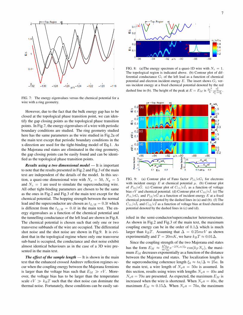
FIG. 7: The energy eigenvalues versus the chemical potential for awire with a ring geometry.
However, due to the fact that the bulk energy gap has to beclosed at the topological phase transition point, we can iden-tify the gap closing points as the topological phase transitionpoints. In Fig.7, the energy eigenvalues of a wire with periodicboundary conditions are studied. The ring geometry studiedhere has the same parameters as the wire studied in Fig.2a ofthe main text except that periodic boundary conditions in thex-direction are used for the tight-binding model of Eq.1. Asthe Majorana end states are eliminated in the ring geometry,the gap closing points can be easily found and can be identi-fied as the topological phase transition points.
Results using a two dimensional model — It is importantto note that the results presented in Fig.2 and Fig.3 of the maintext are independent of the details of the model. In this sec-tion, a quasi-one dimensional wire with Nx = 50, Ny = 5and Nz = 1 are used to simulate the superconducting wire.All other tight-binding parameters are chosen to be the sameas the ones in Fig.2 and Fig.3 of the main text except for thechemical potential. The hopping strength between the normallead and the superconductor are chosen as tL/R = 0.3t whichis different from the tL/R = 0.4t in the main text. The en-ergy eigenvalues as a function of the chemical potential andthe tunnelling conductance of the left lead are shown in Fig.8.The chemical potential is chosen such that only one or twotransverse subbands of the wire are occupied. The differentialshot noise and the shot noise are shown in Fig.9. It is evi-dent that in the topological regime where only one transversesub-band is occupied, the conductance and shot noise exhibitalmost identical behaviours as in the case of a 3D wire pre-sented in the main text.
The effect of the sample length — It is shown in the maintext that the enhanced crossed Andreev reflection regimes oc-cur when the coupling energy between the Majorana fermionsis larger than the voltage bias such that EM � eV . More-over, the voltage bias has to be larger than the temperaturescale eV � kBT such that the shot noise can dominate thethermal noise. Fortunately, these conditions can be easily sat-
FIG. 8: (a)The energy spectrum of a quasi-1D wire with Nz = 1.The topological region is indicated above. (b) Contour plot of dif-ferential conductance G1 of the left lead as a function of chemicalpotential and electron incident energy E. The insert shows G1 ver-sus incident energy at a fixed chemical potential denoted by the red
dashed line in (b). The height of the peak at E = EM is 2e2
h
t2Lt2L+t2
R.
FIG. 9: (a) Contour plot of Fano factor P11/eG1 for electronswith incident energy E at chemical potential µ. (b) Contour plotof P12/eG. (c) Contour plot of C11/eI1 as a function of voltagebias eV and chemical potential. (d) Contour plot of C12/eI . (e) TheP11/eG1 and P12/eG as a function of incident energy E at a fixedchemical potential denoted by the dashed lines in (a) and (b). (f) TheC11/eI1 and C12/eI as a function of voltage bias at fixed chemicalpotential denoted by the dashed lines in (c) and (d).
isfied in the semi-conductor/superconductor heterostructure.As shown in Fig.2 and Fig.3 of the main text, the maximumcoupling energy can be in the order of 0.1∆ which is muchlarger than kBT . Assuming that ∆ = 0.25meV as shownexperimentally and T = 20mK, we have kBT ≈ 0.01∆.
Since the coupling strength of the two Majorana end stateshas the form EM ≈ ~2kF
m∗ξ0e−2Nxa/ξ0 cos(kFNx), the maxi-
mumEM decreases exponentially as a function of the distancebetween the Majorana end states. The localization length isthe superconducting coherence length ξ0 ≈ ta/∆ ≈ 25a. Inthe main text, a wire length of Nxa = 50a is assumed. Inthis section, results using wires with lengths Nxa = 40a andNxa = 70a are presented. As expected, the maximum EM isincreased when the wire is shortened. When Nxa = 40a, themaximum EM ≈ 0.15∆. When Nxa = 70a, the maximum

8
FIG. 10: Nx = 40 for (a) and (b). Nx = 70 for (c) and (d). (a) and(c), Contour plots of C11/eI1 as a function of voltage bias eV andchemical potential. (b) and (d), Contour plots of C12/eI .
EM is reduced to about 0.05∆ and the crossed Andreev re-flection regime is more difficult to observe. Nevertheless, thelength of the wire should not be much shorter than the super-conducting coherence length. Otherwise, the current-current
correlations between the two leads can be significant even inthe absence of Majorana fermions. For example, it is evidentfrom Fig.10b and Fig.10d that C12/I in the topologically triv-ial regime of the shorter wire with Nxa = 40a is much largerthan C12/I in the topologically trivial regime of the wire withNxa = 70a.
∗ Correspondence address to: [email protected]† Correspondence address to: [email protected]
[1] C. J. Bolech and E. Demler, Phys. Rev. Lett. 98, 237002 (2007).[2] J. Nilsson, A. R. Akhmerov, and C. W. J. Beenakker, Phys. Rev.
Lett. 101,120403 (2008).[3] K.T. Law, P.A. Lee, T.K. Ng Phys. Rev. Lett. 103,237001 (2009).[4] V. Mourik, K. Zuo, S.M. Frolov, S.R. Plissard, E.P.A.M.
Bakkers, L.P. Kouwenhoven, Science 336, 1003 (2012).[5] H. O. H. Churchill, V. Fatemi, K. Grove-Rasmussen, M. T. Deng,
P. Caroff, H. Q. Xu, C. M. Marcus, arXiv:1303.2407.[6] A. C. Potter and P. A. Lee, Phys. Rev. B 83, 094525 (2011).[7] D. Rainis, L. Trifunovic, J. Klinovaja, D. Loss Phys. Rev. B 87,
024515 (2013).[8] S. Das Sarma, J. D. Sau, T. D. Stanescu, Phys. Rev. B 86, 220506
(2012).


![[Papercraft] Banco da China, Hong Kong](https://img.dokumen.tips/doc/110x75/55288796550346bc588b484b/papercraft-banco-da-china-hong-kong.jpg)