Embed Size (px)
Citation preview

MOSFET LF NOISE UNDER LARGE SIGNAL EXCITATION
MEASUREMENT, MODELLING AND APPLICATION
Arnoud van der Wel

Samenstelling promotiecommissie:
Voorzitter: prof.dr.ir. J. van Amerongen Universiteit Twente, EWI
Secretaris: prof.dr.ir. A.J. Mouthaan Universiteit Twente, EWI
Promotor: prof.dr.ir. B. Nauta Universiteit Twente, EWI
Assistent Promotor: dr.ing. E.A.M. Klumperink Universiteit Twente, EWI
Referent: dr. R. Woltjer Philips Research, Eindhoven
Leden: prof.dr. H. Wallinga Universiteit Twente, EWIprof.dr.ir. C.H. Slump Universiteit Twente, EWIprof.dr.ir. A.J.P. Theuwissen TU Delftprof.dr. J. Schmitz Universiteit Twente, EWI
Title: MOSFET LF NOISE UNDER LARGE SIGNAL EXCITATION:MEASUREMENT, MODELLING AND APPLICATION
Author: Arnoud van der Wel
ISBN: 90-365-2173-4
This research was supported by the Technology Foundation STW, appliedscience division of NWO and the technology programme of the Ministry ofEconomic Affairs.

MOSFET LF NOISE UNDER LARGE SIGNAL EXCITATION
MEASUREMENT, MODELLING AND APPLICATION
PROEFSCHRIFT
ter verkrijging vande graad van doctor aan de Universiteit Twente,
op gezag van de rector magnificus,prof.dr. W.H.M. Zijm,
volgens besluit van het College voor Promotiesin het openbaar te verdedigen
op 15 april 2005 om 15.00 uur
door
Arnoud Pieter van der Welgeboren op 31 mei 1974
te Bunschoten

Dit proefschrft is goedgekeurd door:
de promotor prof.dr.ir. B. Nauta
de assistent promotor dr.ing. E.A.M. Klumperink

Contents
List of Symbols v
List of Abbreviations ix
Samenvatting xi
1 Introduction 1
1.1 Noise is everywhere . . . . . . . . . . . . . . . . . . . . . 1
1.2 LF noise and analog circuit design . . . . . . . . . . . . . 3
1.3 Scope of this thesis . . . . . . . . . . . . . . . . . . . . . 4
2 Background 7
2.1 Introduction . . . . . . . . . . . . . . . . . . . . . . . . . 7
2.2 Time and frequency domain analysis . . . . . . . . . . . . 7
2.3 Stochastic signals . . . . . . . . . . . . . . . . . . . . . . 9
2.4 MOSFETs . . . . . . . . . . . . . . . . . . . . . . . . . . 17
2.5 LF noise modelling . . . . . . . . . . . . . . . . . . . . . 20
2.6 The future of LF noise in MOSFETs . . . . . . . . . . . . 26
2.7 Conclusion . . . . . . . . . . . . . . . . . . . . . . . . . 29
3 Measurement of LF noise under large signal excitation 31
3.1 Introduction . . . . . . . . . . . . . . . . . . . . . . . . . 31
i

CONTENTS
3.2 Measures for LF noise . . . . . . . . . . . . . . . . . . . 32
3.3 Review of published measurement results . . . . . . . . . 39
3.4 Large signal bias factors and their influence on LF noise . 42
3.5 Device factors and their influence on LF noise . . . . . . . 53
3.6 Spread in LF noise under large signal excitation . . . . . . 55
3.7 Conclusion . . . . . . . . . . . . . . . . . . . . . . . . . 60
4 Modelling 63
4.1 Introduction . . . . . . . . . . . . . . . . . . . . . . . . . 63
4.2 Model . . . . . . . . . . . . . . . . . . . . . . . . . . . . 64
4.3 Analytical . . . . . . . . . . . . . . . . . . . . . . . . . . 66
4.4 Cyclostationary RTS noise Simulator . . . . . . . . . . . . 74
4.5 Conclusion . . . . . . . . . . . . . . . . . . . . . . . . . 90
5 Perspective on application 91
5.1 Introduction . . . . . . . . . . . . . . . . . . . . . . . . . 91
5.2 Time-continuous circuits . . . . . . . . . . . . . . . . . . 93
5.3 Time-discrete circuits . . . . . . . . . . . . . . . . . . . . 100
5.4 Large-signal circuits . . . . . . . . . . . . . . . . . . . . 110
5.5 Novel applications of LF noise under LSE . . . . . . . . . 119
5.6 Characterization of LF noise . . . . . . . . . . . . . . . . 120
5.7 Conclusion . . . . . . . . . . . . . . . . . . . . . . . . . 122
6 Conclusion 125
6.1 Summary of conclusions . . . . . . . . . . . . . . . . . . 125
6.2 Original contributions of this thesis . . . . . . . . . . . . . 127
A Noise performance of CDS circuit. 129
Bibliography 135
ii

List of Publications 143
Dankwoord 147
About the Author 149
iii


List of Symbols
Symbol Explanation Units
1 Heaviside unit step function –
A Area of MOSFET (=WL) m2
B Bandwidth Hz
C Channel capacity bits s−1
Cox Oxide capacitance per square meter Fm−2
Cxx Autocovariance of a stochastic signalx(t)
dc Duty cycle, between 0 and 1 –
f (E, t) Occupancy function of traps at energylevel E and time t
–
fc 1/ f noise corner frequency, whereS1/f = Sth.
Hz
fs Sample frequency (= 1/ts) Hz
gm Transconductance AV−1
h Planck’s constant, 6.62×10⁻³⁴ Js−1
ID Drain current A
k Boltzmann’s constant, 1.38×10⁻²³ JK−1
K Arbitrary constant –
L Length of MOSFET m
m τ change factor between two bias statesof MOSFET (me and mc are for τe and τc
respectively)
–
v

LIST OF SYMBOLS
Symbol Explanation Units
mx Average value of a stochastic signal x
n Electron concentration m−3
N Noise power W
N Total number of free carriers in a sample –
Nc Effective density of states in theconduction band
m−3
Nlin Total number of free carriers inMOSFET in linear region
–
Nsat Total number of free carriers inMOSFET in saturation
–
N Number of free carriers per unit area m−2
P Power W
q Elementary charge, 1.6×10⁻¹⁹ C
QSS Charge stored in surface states C
rc(E, t) Capture rate s−1
re(E, t) Emission rate s−1
R Resistance ΩRxx Autocorrelation of a stochastic signal
x(t)
RRTS Autocorrelation function of RTS
s Scaling factor from current to futureCMOS process generation (> 1)
–
S Signal power W
Sx Power Spectral Density of x W Hz−1
S1/f Power Spectral Density of 1/ f noise W Hz−1
Sth Power Spectral Density of thermal noise W Hz−1
S∆N Power Spectral Density of ∆N Hz−1
S∆N Power Spectral Density of ∆N per unit
areaHz−1m−2
SQSS Power Spectral Density of QSS C2Hz−1
T Period of a periodic signal s
vi

Symbol Explanation Units
Absolute temperature K
ts Sample time (= 1/ fs) s
vth Thermal velocity of electrons ms−1
VDS Drain to Source voltage V
VGT Gate overdrive voltage: VG-VT V
var(x) Variance of a stochastic signal x(t)
W Width of MOSFET m
x( f ) Frequency domain description of signal Hz−1
x(t) Time domain description of signal
α Coupling coefficient between numberand mobility fluctuations used in theHung LF noise model
–
αH Hooge empirical factor –
β Asymmetry factor of RTS; 1 forsymmetric RTS
–
µ Mobility of mobile charge carriers m2 V−1 s−1
σ Conductivity CV−1s−1m−1
σVT Standard deviation of VT V
σ(E,x) Capture cross section of trap m2
τc Mean time before capture event occurs s
τe Mean time before emission event occurs s
τeff,on Time constant of occupancy changewhen device is ’on’
s
τeff,off Time constant of occupancy changewhen device is ’off’
s
ω0RTS RTS corner frequency rad s−1
ξ Channel thermal noise form factor, ≥ 1 –
vii

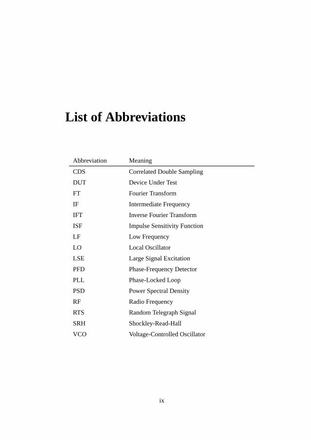
List of Abbreviations
Abbreviation Meaning
CDS Correlated Double Sampling
DUT Device Under Test
FT Fourier Transform
IF Intermediate Frequency
IFT Inverse Fourier Transform
ISF Impulse Sensitivity Function
LF Low Frequency
LO Local Oscillator
LSE Large Signal Excitation
PFD Phase-Frequency Detector
PLL Phase-Locked Loop
PSD Power Spectral Density
RF Radio Frequency
RTS Random Telegraph Signal
SRH Shockley-Read-Hall
VCO Voltage-Controlled Oscillator
ix


Samenvatting
Moderne elektronische schakelingen maken veelal gebruik van CMOS tech-nologie waarin MOSFETs fungeren als actieve elementen. Het gebruik vaneen MOSFET als versterkend element biedt behalve veel voordelen zoalsde lage kosten, de hoge snelheid, en de goede integreerbaarheid ook nade-len, met name de notoire laagfrequente ruis ervan. Het laagfrequent (LF)ruisgedrag van MOSFETs wordt gedomineerd door plaatsgebonden ener-gietoestanden (‘traps’) aan de Si-SiO2 grenslaag die een elektron tijdelijkkunnen invangen en daarmee de geleiding van de MOSFET beınvloeden.In dit proefschrift wordt de LF ruis van MOSFETs bestudeerd onder groot-signaal biascondities.
Onder grootsignaal biascondities vertonen MOSFETs vaak een afname inLF ruis. Bovendien komen grootsignaal biascondities nauw overeen metde manier waarop MOSFETs in echte schakelingen gebruikt worden. Aandrie belangrijke punten wordt in dit proefschrift aandacht besteed. Ten eer-ste: Hoe kan LF ruis onder grootsignaal biascondities gemeten worden, tentweede: Hoe komt het dat de ruis vaak afneemt onder grootsignaal biascon-dities, en tot slot: Is de LF ruisreductie significant en bruikbaar genoeg omtoe te passen bij het ontwerp van analoge schakelingen met MOSFETs?
In hoofdstuk 3 wordt ingegaan op het meten van LF ruis onder grootsig-naal biascondities. Tevens worden daar de belangrijkste meetresultaten ge-presenteerd. Het meten van LF ruis onder grootsignaal condities stelt hogeeisen aan het dynamisch bereik van de meetopstelling omdat de LF ruis veelkleiner is dan de tijdvariante bias. Er worden drie methoden toegepast. Teneerste kan door differentieel te werken, het bias signaal gemeenschappe-lijk aangeboden worden, terwijl de ruis differentieel blijft. Op deze wijzewordt het gemeenschappelijke signaal door de meetopstelling onderdrukt,en wordt het mogelijk de ruis te meten. Ten tweede kan de ruis van hetbias-signaal gescheiden worden in de tijd, dus er wordt eerst een bias-puls
xi

SAMENVATTING
aangeboden en kort daarna wordt de ruis gemeten, en tot slot kan de ruis enhet bias-signaal in frequentie gescheiden worden: de ruis is laagfrequent enhet bias-signaal hoogfrequent.
Met behulp van deze meetmethoden worden metingen gepresenteerd aanverschillende MOSFETs. Waar grote MOSFETs systematisch een afna-me van de LF ruis vertonen in grootsignaal bedrijf, is het gedrag van kleineMOSFETs met een oppervlak van ver onder de 1µm2 veel minder voorspel-baar. Deze transistoren vertonen al in de stationaire toestand veel variatiein hun LF ruis, en bovendien is niet met zekerheid van te voren vast te stel-len hoe ze zullen reageren op grootsignaal biascondities. Meestal neemtde LF ruis af, maar soms neemt deze ook toe. Dit komt omdat het gedragvan deze transistoren door slechts een of enkele ‘traps’ gedomineerd wordt.Zowel n- als p-kanaals MOSFETs vertonen soortgelijk gedrag, hetgeen erop duidt dat het ruisgenererende proces hetzelfde is. Tevens wordt gemetendat het periodiek varieren van zowel de ‘gate’ als de ‘source’ spanning vande MOSFET een vergelijkbaar effect heeft op de LF ruis ervan.
In hoofdstuk 4 wordt een verklaring gepresenteerd voor de meetresultatenaan de hand van de al eerder genoemde ‘traps’, waarvan het gedrag wordtbeschreven door de Shockley-Read-Hall theorie. Aan de hand van dezetheorie, toegepast onder grootsignaal biascondities, wordt aangetoond datde ruis onder grootsignaal biascondities wordt gedomineerd door traps diezich dichter bij het midden van de bandgap bevinden. Aangezien de trap-dichtheid in het midden van de bandgap vaak lager is dan in de buurt vande geleidingsband, kan zo worden uitgelegd dat de ruis gemiddeld gezienafneemt in grootsignaal bedrijf. Om de voorspellingen van het model tetoetsen wordt een simulator beschreven die in staat is het gedrag van detransistoren nauwkeurig te reproduceren. Ook transitief ruisgedrag is goedte begrijpen op basis van het model en de simulator.
Als laatste wordt in hoofdstuk 5 aandacht besteed aan de vraag of groot-signaal excitatie voor circuitontwerpers praktisch toepasbaar is om LF ruisvan MOSFETs tegen te gaan. In tijdcontinue schakelingen blijkt het moge-lijk grootsignaal excitatie als ruisreductietechniek te gebruiken, maar moetvergeleken worden met een modulerende structuur die de LF ruis geheelverwijdert. Het gebruik van grootsignaal excitatie in dit soort situaties isdan ook niet zonder meer aan te bevelen. In tijddiscrete schakelingen is heteveneens mogelijk grootsignaal excitatie nuttig toe te passen als ruisreductietechniek, temeer daar de schakeling tussen de samplemomenten uitgescha-keld kan worden, en er zodoende geen noemenswaardige bezwaren aan hetgebruik ervan kleven. Bij ‘correlated double sampling’ structuren moet er
xii

voor gezorgd worden dat de biasgeschiedenis van beide samplemomentenidentiek is, daar de ruis anders eerder toe dan af zal nemen. Ook hoogfre-quent schakelingen hebben last van LF ruis door ‘opconversie’ van de ruis.Aangezien de LF ruisreductie niet gevoelig blijkt te zijn voor de frequentiewaarmee de MOSFET aan en uit gezet wordt, kan in deze schakelingen ooknuttig gebruik gemaakt worden van grootsignaal excitatie als ruisreductietechniek.
Hoewel ruisreductie door grootsignaal excitatie weliswaar een meetbare af-name van de LF ruis van MOSFETs oplevert, is de winst beperkt en afhan-kelijk van het proces in kwestie. Om grootsignaal excitatie ten behoeve vanruisreductie nuttig toe te kunnen passen moet eerst een voldoende nauw-keurig stationair LF ruismodel beschikbaar zijn. Vervolgens moet het LFruisgedrag van het proces in kwestie onder grootsignaal condities gekarak-teriseerd worden.
xiii

Chapter 1
Introduction
1.1 Noise is everywhere
Whenever people communicate, whether by smoke signals, waving theirhands, shouting, using a satellite phone or an optical fiber, noise limits howwell they can communicate and how much effort is needed to get the messa-ge across. If you are shouting to someone on the other side of a busy road,the noise of the traffic makes it difficult to communicate. You will eitherhave to raise your voice, speak more slowly or repeat yourself if you wantto be understood.
Electronic circuits are limited by noise in much the same way. Goingagainst my firm conviction that equations do not belong in a introducti-on, I will present to you what is perhaps the single most important equationin the field of information theory. Indeed, this is the equation that definesinformation theory and that is therefore at the foundation of our moderninformation society. It was proposed by Claude Shannon in 1948 [58]1:
C = B log2
(1+
SN
)(1.1)
This equation features prominently in the first few pages of any text oninformation or communication theory, so it is not necessary to discuss itin any depth here. The form of the equation is recognizable, however. Itformalizes what was said in the first paragraph, namely that how well you
1It is fortunate that Shannon chose to publish his work at all, since he was reportedly nonetoo impressed with it, and published it only after repeated urging from colleagues.
1

1. INTRODUCTION
can communicate (C) depends on how much effort you spend (S) and whatthe noise level is (N).
Noise then, if you like, is the foundation of the foundation.
Not only in information theory does noise occupy a central position, but al-so in physics. Any dissipative element exhibits thermal noise. This includes(but is not limited to): wires, resistors, transistors, diodes, inductors, capa-citors, transformers, MOSFETs, and opamps. It is a safe bet that if it canbe soldered, requires batteries or can be plugged into the mains, it exhibitsthermal noise.
Thermal noise is not the only type of noise, however. Many componentsexhibit excess noise at low frequencies. The term ‘excess’ indicates ‘mo-re than expected from the theory of thermal noise’. This excess noise isvariously referred to as ‘flicker noise’ or ‘LF noise’, and it includes suchphenomena as 1/ f and Random Telegraph Signal (RTS) noise.
The low frequency (LF) noise of MOSFETs is particularly interesting: amodern MOSFET is so small that the effects of single electrons can beseen. One example of such noise is in figure 1.1.
Time →
Cur
rent
→
Figure 1.1: LF noise of a 0.18 µm2 MOSFET. The abrupt jumps are causedby single electrons. Superimposed on this are other types of noise.
It is remarkable that single electron effects can be observed so easily: the ex-periment takes place at room temperature, and apart from one minimal-areaMOSFET (the CPU in your computer contains tens of millions of these),you only need a preamplifier (e1.50) and an oscilloscope.
LF noise in MOSFETs is not only fascinating for the detailed view it provi-des into the chaotic interior of the MOSFET, but it also gets a lot of attentionbecause it forms a significant limitation to the practical use of the MOSFETin an electronic circuit.
2

LF noise and analog circuit design
1.2 LF noise and analog circuit design
Design of analog CMOS circuits is a complex tradeoff between resourcesand goals. The aim is typically to realize a high speed, high accuracy design,with minimal expenditure of supply power and chip area. In this context,an optimal design is one that expends minimal resources to just achievethe specified goals. If specifications are not met the design is unsuccessfuland if specifications are exceeded, or if the specifications are met whilstexpending more than the minimally required resources, the design is notoptimal. In the search for design optimality, it is extremely useful to knowwhere the physical limits are so one can strive to reach them, and at thesame time ensure that the physically impossible is not attempted.
In CMOS, the smallest signal that can be reliably processed depends onthe noise of the MOSFET. The MOSFET’s dominant sources of noise arethermal noise due to the dissipative character of the conducting channel andLF noise.
LF noise in MOSFETs has been studied for many decades. There is ampledata indicating the presence of a bulk 1/ f noise source in homogenoussemiconductor samples [26]. It it reasonable to assume this is also presentin a MOSFET, however MOSFET LF noise behaviour is dominated by thesilicon surface, at the interface between the silicon and the gate oxide. TheSi-SiO2 interface is imperfect for at least two reasons. First, the crystallinestructure of Si does not fit the amorphous SiO2 and this leads to so-called‘dangling bonds’. Secondly, during processing, impurities are introducedat the interface and in the oxide. Both mechanisms give rise to localizedenergy states known as ‘traps’. These traps generate the RTS noise of figure1.1 that dominates MOSFET LF noise behaviour.
In 1991, it was noted for the first time [6, 7] that MOSFET LF noise isreduced when the device is subjected to large signal excitation (LSE). Inother words, turning it ‘off’ for some time before turning it ‘on’ reduces itsnoise when it is ‘on’. This means that the LF noise of the device not onlydepends on the present bias state of the device but also on the bias historyof the device. Soon afterwards this effect was associated with the emptyingof traps that cause RTS noise [14]. In 1996, the effect was independentlydiscovered by Hoogzaad and Gierkink at the University of Twente [19],leading to a demonstration of the LF noise reduction effect by LSE in a ringoscillator [20] and in a coupled sawtooth oscillator [36].
3

1. INTRODUCTION
1.3 Scope of this thesis
In this thesis, we cover the issues that need to be addressed before LF noisereduction by LSE can be applied to analog circuit design. Detailed physicalmodelling of trap behaviour under LSE is given in [38].
For a long time, Moore’s self-fulfilling prophecy [52] has made MOSFETdimensions go down according to a fairly well described exponential curve.This is not only very important to device physicists who use this curve topredict what process hurdles will need to be overcome and when this willneed to be done, but it is also very interesting for people designing analogcircuitry.
In chapter two, an introduction is given to the mathematics and physics ofLF noise in MOSFETs.
Existing LF noise models are combined with what is known about CMOSprocess downscaling, which allows predictions to be made as to what willbe the dominant problems in future process generations. From this, weshow that LF noise, in contrast to many other problems, is not somethingMoore’s ‘law’ will automatically solve, thereby justifying the work in thisthesis.
Before LF noise under large signal excitation can be understood, data needsto be gathered. LF noise shows considerable spread: different nominallyidentical devices may have LF noise powers that vary by several orders ofmagnitude. For small-area devices, the spread is worse. This makes LFnoise characterization challenging: it is not possible to characterize a singledevice and generalize its behaviour; large numbers of devices are requiredbefore general conclusions can be drawn. LF noise behaviour under LSE isalso very variable: not only the magnitude of the noise change varies, butthe direction as well: sometimes subjecting a device to LSE will increaseits LF noise, while other devices show an LF noise decrease under the sameconditions.
p-Channel devices are sometimes favoured by designers because they ex-hibit less LF noise than n-channel devices. Also, it is often noted thatp-channel devices have LF noise that can best be explained using the ∆µmodel, whereas n-channel devices are often seen to behave in accordancewith the ∆N model. In the light of these discrepancies, it is by no meanscertain that LF noise under LSE will behave in the same manner in bothtypes of devices.
In chapter three, LF noise measurements under LSE for both device types
4

Scope of this thesis
are compared. Another issue that is investigated is the relation between thechange in LF noise under LSE and how the LSE is applied to the device:which device terminals allow the LF noise to be influenced? Finally, largenumbers of nominally identical devices are measured and the spread of theirLF noise and their LF noise under LSE is characterized.
Having characterized the effect, it needs to be removed from the realm of‘just another interesting effect’ to something that can be related to establis-hed device parameters. Initially, not a lot was known about the physicalorigins of the LF noise measured, but it rapidly became apparent in mea-surements that the noise observed was RTS-dominated. Both in the timedomain where the characteristic two-level signal of an RTS was observed,and in the frequency domain, where the shape of the LF noise power spec-tral density was seen to vary between f 0 and f−2.
In chapter four, the experimental observations are related to the vast amountof known data on the subject of interface traps. This allows us to modelwhy the LF noise usually decreases under LSE: LF noise under LSE probestraps nearer the center of the bandgap, and the trap density there is lowerthan near the bandgap edge. With our model, based on Shockley-Read-Halltheory applied under non-steady-state conditions, LF noise behaviour underLSE follows logically from the characteristics of the device, and no addi-tional fitting parameters are required. An LF noise simulator based on thesame model is also presented.
Regarding application of LF noise reduction by LSE, the important questi-on to be answered is of course how it compares to established techniques.Unfortunately, on the whole, the established noise reduction techniques arequite effective at reducing noise, so competing with them is no trivial task.In addition, while LF noise reduction by LSE showed great promise in olderprocesses, the noise reduction in newer CMOS processes is much lower. Incorrelated double sampling circuits, LSE may be applied but only in such away that the bias history for both sample moments is identical. When thisis not the case LSE is shown to be more likely to increase than to decreasethe noise. Only in RF circuits, where other techniques are not applicabledoes LF noise reduction by LSE show some promise, especially since thefrequency of the LSE is not important for the LF noise performance.
In chapter five, the different ways in which LF noise reduction by LSE canbe applied to analog circuit design are explored. Three classes of circuitsare discussed and the applicability of LF noise reduction by LSE in eachclass is treated. Though LF noise reduction by LSE can provide a benefitin specific cases, the accuracy of steady state LF noise models still needs to
5

1. INTRODUCTION
improve a lot before the limited benefits of the LSE technique can becomeuseful.
6

Chapter 2
Background
2.1 Introduction
In this chapter, the mathematical and physical background to the remain-der of this work will be presented. We start with a brief summary of someimportant concepts in time and frequency domain analysis. Having donethat, some important concepts in stochastics are reviewed. Next, the clas-sical MOSFET square law approximation that forms the basis for a lot ofthe classical LF noise modelling work is presented. Finally, the future ofLF noise in MOSFETs is treated. The framework presented in this chapterforms the basis for the modelling work in chapter 4.
2.2 Time and frequency domain analysis
A brief review of some important concepts in frequency domain analysisis presented. More exhaustive treatment of the subject matter can be foundin [12] or other textbooks.
Units of the Fourier Transform.
The Fourier transform is the basis of frequency domain analysis. Using theFourier transform we can analyse signals in the frequency and in the timedomain, however some care is required in the use of units. The Fourier
7
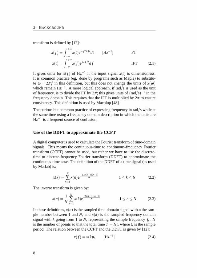
2. BACKGROUND
transform is defined by [12]:
x( f ) =∫ +∞
−∞x(t)e− j2π f tdt [Hz−1] FT
x(t) =∫ +∞
−∞x( f )e j2π f td f IFT (2.1)
It gives units for x( f ) of Hz−1 if the input signal x(t) is dimensionless.It is common practice (eg. done by programs such as Maple) to substitu-te ω = 2π f in this definition, but this does not change the units of x(ω)which remain Hz−1. A more logical approach, if rad/s is used as the unitof frequency, is to divide the FT by 2π; this gives units of (rad/s)−1 in thefrequency domain. This requires that the IFT is multiplied by 2π to ensureconsistency. This definition is used by Machlup [48].
The curious but common practice of expressing frequency in rad/s while atthe same time using a frequency domain description in which the units areHz−1 is a frequent source of confusion.
Use of the DDFT to approximate the CCFT
A digital computer is used to calculate the Fourier transform of time-domainsignals. This means the continuous-time to continuous-frequency Fouriertransform (CCFT) cannot be used, but rather we have to use the discrete-time to discrete-frequency Fourier transform (DDFT) to approximate thecontinuous-time case. The definition of the DDFT of a time signal (as usedby Matlab) is:
x(k) =N
∑n=1
x(n)e− j2π(k−1)(n−1)
N 1 ≤ k ≤ N (2.2)
The inverse transform is given by:
x(n) =1N
N
∑k=1
x(k)ej2π(k−1)(n−1)
N 1 ≤ n ≤ N (2.3)
In these definitions, x(n) is the sampled time-domain signal with n the sam-ple number between 1 and N, and x(k) is the sampled frequency domainsignal with k going from 1 to N, representing the sample frequency fs. Nis the number of points so that the total time T = Nts where ts is the sampleperiod. The relation between the CCFT and the DDFT is given by [12]:
x( f ) = x(k)ts [Hz−1] (2.4)
8

Stochastic signals
The DDFT will cover the frequency range of 0 to fs/2 in N/2 steps. Thefrequency resolution (distance between adjacent samples in the frequencydomain) is 1/T [Hz]. This is also the lowest frequency measurable.
One-and two sided frequency domain description of signals
A common cause of confusion is the indiscriminate mix of one- and two-sided frequency domain descriptions. The Fourier transform, which in es-sence defines the frequency domain, gives rise to a frequency domain de-scription of the signal that goes from f = −∞ . . .+∞, and this is mathe-matically the most complete way of describing a signal in the frequencydomain. If x(t) is real, however, x( f ) will have a negative half that is thecomplex conjugate of the positive half. In these cases, giving the completex( f ) is redundant, and it is sufficient to give only the positive half of x( f ).To preserve the total energy of the signal, x( f ) is then multiplied by
√2.
The resultant x( f ) is known as ‘one-sided’. For real signals, a one-sidedfrequency-domain description is convenient and adequate. However, whentransforming back to the time domain, it is important that the appropriateintegration limits be used: −∞ and +∞ for a two-sided x( f ) and 0 and +∞for a one-sided x( f ).
2.3 Stochastic signals
In describing noise, it is useful to briefly review some important conceptsin stochastics. A stochastic signal is random; i.e. the value of the signal at aparticular time cannot be predicted. The signal can, however, be describedin terms of its stochastic parameters. Some useful stochastic parameters aredefined in this section. Random signals are then examined in the frequencydomain, and finally some important random signals (RTS noise and 1/ fnoise) are discussed in terms of the definitions given.
Describing stochastic signals.
The expected value of a random signal x(t) is its time average. It is givenby
E [x(t)] = limT→∞
1T
∫ T/2
−T/2x(t)dt (2.5)
9

2. BACKGROUND
The nth moment of a signal is the expected value of x(t)n. It is given by:
E[x(t)n] = limT→∞
1T
∫ T/2
−T/2x(t)ndt (2.6)
Some common moments are:
• The 1st moment of x(t) is its average, often denoted by mx.• The 2nd moment of x(t) is the total power of the signal.• The 2nd moment of [x(t)−mx] is its variance, var(x). This is the AC
power of the signal.
Higher order moments may be used for mathematical and formal comple-teness, but they have limited practical significance.
The autocorrelation function of a signal is defined by:
Rxx(t, t + τ) = E [x(t) x(t + τ)] (2.7)
Rxx(t, t) =E [x(t) x(t)]
=E[x(t)2]
=2nd moment of x(t)=total power of the signal (2.8)
In a similar way, the autocovariance is given by:
Cxx(t, t + τ) = E [(x(t)−mx) (x(t + τ)−mx)] (2.9)
Cxx(t, t) =E [(x(t)−mx) (x(t)−mx)]
=E[(x(t)−mx)2]
=var(x) (2.10)
The autocorrelation function and the autocovariance function differ only inthat the autocorrelation function encompasses DC whereas the autocova-riance function does not. The autocorrelation function is therefore morecomplete, and the autocovariance function should only be used in caseswhere the random signal in question has a non-zero mean and the intent isspecifically to disregard this mean.
Ergodicity, stationarity and cyclostationarity
A random signal is said to be stationary if the moments of the random signalare not a function of time. A signal is ‘strictly stationary’ if this is satisfied
10

Stochastic signals
for all its moments. A signal is ‘wide-sense stationary’ if this is satisfied forall moments up to and including the second moment.
If a signal is stationary, the autocorrelation function given in eq. 2.7 will nolonger be a function of the absolute time t but only of the time difference τ:
Rxx(t, t + τ) = Rxx(τ) (2.11)
A random signal is said to be ergodic if the ensemble average (average overa number of realizations) is equal to the time average of one realization ofthe signal. A signal is wide-sense ergodic if the first and second momentsare ergodic, and ergodic in the strict sense if all its moments are ergodic.If a random signal is ergodic, it must also be stationary. A signal whosemoments are periodic in T is said to be cyclostationary in T .
Frequency domain analysis of stochastic signals: the PSD
The PSD and the Wiener-Khinchin theorem
The Power Spectral Density (PSD) of a signal is a plot of the power perunit of bandwidth against frequency. The units of a PSD are W Hz−1. Theunits V2Hz−1 or A2Hz−1 also find common usage, in those cases a constantimpedance is assumed. The Wiener-Khinchin theorem allows us to go fromthe time domain to the frequency domain. It states that the PSD of a signalis the Fourier transform of the autocorrelation function.
Sx( f ) = FT(Rxx(t, t + τ)) (2.12)
The power of the signal in the frequency domain and in the time domainis equal, as shown by equation 2.13. Care must be taken to use the correctunits for Sx( f ). If integrating over f , the units for Sx( f ) must be in terms ofpower per Hertz. ∫ +∞
−∞Sx( f )d f = Psignal = E
[x(t)2] (2.13)
The PSD can also be calculated without first calculating the autocorrelationfunction. This is sometimes referred to as the ‘direct’ way of calculatingthe PSD [12]:
Sx( f ) = limT→∞
|x( f )|2T
(2.14)
The PSD contains less information than the time-domain signal. The firstway of calculating the PSD (eq. 2.12) discards information when the au-tocorrelation function Rxx is computed; different time domain signals may
11

2. BACKGROUND
have the same autocorrelation function. The second way of calculating thePSD (eq. 2.14) discards phase information by taking the magnitude of x( f ).Though the PSD of a random signal is very useful, a time-domain descrip-tion is formally more complete.
The PSD of a cyclostationary signal
A signal which is cyclostationary in T will have moments that are periodicin T . The autocorrelation function of such a cyclostationary signal will alsobe periodic in T ; i.e.
Rxx(t, t + τ) = Rxx(t +T, t +T + τ) (2.15)
Additionally, the autocorrelation function at any particular time t will ha-ve periodic components. Such an autocorrelation function can in theory beused to calculate the time-variant PSD of the cyclostationary signal by ri-gourous application of the Wiener-Khinchin theorem, but this not alwaysnecessary. A more productive approach is often to first ‘stationarize’ thesignal by averaging the moments of the signal over one period, and thenFourier transforming to find the ‘stationarized’ PSD [16]. Stationarizingthe signal may equivalently be done by modelling the time reference as arandom variable that is uniformly distributed over one cycle. The observer,in both cases, has no knowledge anymore of the phase of the signal. Thisapproach is therefore valid whenever the ‘measuring’ system is not synchro-nized with the cyclostationary noise source, for example when a spectrumanalyser is used to measure cyclostationary noise.
Random Telegraph Signals
A Random Telegraph Signal (RTS) is shown in fig. 2.1. It is a time-continuous, amplitude-discrete signal. The conditional probability of a tran-sition from one state to another (given that it is in that particular state) isproportional to dt; this makes the time spent in each state (‘1’ and ‘0’ in thefigure) exponentially distributed.
This can be understood as follows: if the conditional probability of a tran-sition from a state, given that the signal is in that state, per unit time, isconstant, then the absolute probability of a transition from that state is pro-
12

Stochastic signals
0
1
stat
e
Time →
Figure 2.1: A Random Telegraph Signal (RTS)
portional to the probability of being in the state. Mathematically:
P(transition) =P(transition|state) P(state)P(transition|state) ∝ dt
P(transition) ∝ P(state)dt
dP(state) ∝ P(state)dt
dP(state)dt
∝ P(state) (2.16)
Equation 2.16 is a first-order differential equation that can be solved to givean exponential P(state)(t).
The RTS is completely characterized by three parameters: The amplitude,the mean ‘high’ time and the mean ‘low’ time. The autocorrelation functionand PSD of an RTS will be derived. The derivation follows Machlup [48].For mathematical convenience, the amplitude is chosen as 1, and the twostates of the RTS are named ‘0’ and ‘1’. The autocorrelation function of theRTS is given by:
RRTS = E [RTS(t) RTS(t + τ)]
= ∑i j
[xi x j P(x(t) = xi) P(x(t + τ) = x j|x(t)=xi
)]
(2.17)
Since one of the states is called ‘0’, three of the four terms in this sumvanish, and we have:
RRTS = 1×1×P(x(t) = 1)×P(ntrans is even, given a start in state 1)= P(x(t) = 1) P11(τ) (2.18)
13

2. BACKGROUND
If the mean ‘high’ time is denoted by τ1 and the mean ‘low’ time by τ0 thenthe probability of being in state ‘1’ at any particular time is given by
P(x(t) = 1) =τ1
τ0 + τ1(2.19)
and the autocorrelation function is found as
RRTS =τ1
τ0 + τ1P11(τ) (2.20)
P11 can be found by first realizing
P11(τ)+P10(τ) = 1 (2.21)
We can then write:
P11(τ +dτ) = P10(τ)dττ0
+P11(τ)(
1− dττ1
)(2.22)
In words: An even number of transitions in time τ +dτ , given that a start ismade in state ‘1’, is possible in two ways: either an odd number of transiti-ons in time τ followed by a transition from ‘0’ to ‘1’ in time dτ , or an evennumber of transitions in time τ followed by no transition from state ‘1’ to‘0’ in time dτ . If the time dτ is made small enough, the probability of morethan one transition in time dτ is negligible. Substituting eq. 2.21, the limitcan then be taken for dτ → 0 to arrive at the differential equation for P11:
dP11
dτ+
(1τ1
+1τ0
)P11 =
1τ0
(2.23)
This differential equation can be solved using the initial condition P11(0) =1 to arrive at:
P11(τ) =1
τ1 + τ0
[τ0e
−(
1τ0
+ 1τ1
)τ + τ1
](2.24)
This leads to:
RRTS(τ) =τ1
(τ1 + τ0)2
[τ0e
−(
1τ0
+ 1τ1
)τ + τ1
](2.25)
Fourier transforming the autocorrelation function, the spectrum of the RTScan be found:
SRTS(ω) =∫ +∞
−∞RRTSe− jωτdτ [Hz−1]
= 2τ0τ1
(τ0 + τ1)2
(1τ0
+ 1τ1
)ω2 +
(1τ0
+ 1τ1
)2 +2π(
τ1
τ0 + τ1
)2
δ (ω) (2.26)
14

Stochastic signals
100
101
102
103
104
100
101
102
103
104
PS
D [A
rbitr
ary
scal
e]→
Frequency [Hz]→
Figure 2.2: PSD of an RTS; f0RTS = 100 Hz
This is a Lorentzian spectrum. Ignoring the DC term and making two sub-stitutions, the result is:
β =τ0
τ1
ω0RTS =1τ0
+1τ1
[rad/s]
SRTS(ω) = 2β
(1+β )2
1ω0RTS
1
1+ ω2
ω20RTS
[Hz−1] (2.27)
A PSD of an RTS is given in fig. 2.2. The LF power of the RTS is inverselyproportional to the RTS corner frequency, ω0RTS. The final term definesthe frequency dependence of the RTS: flat at low frequencies and decayingwith 1/ω2 above the RTS corner frequency. Note that the spectrum of theRTS is symmetrical with respect to τ1 and τ0; only the DC term is sensitiveto the difference. The power of the PSD depends on the ‘asymmetry factor’β . This is shown in fig. 2.3. If β = 1; i.e. τ0 = τ1, the PSD of the RTS willbe at a maximum.
15

2. BACKGROUND
10−2
10−1
100
101
102
10−2
10−1
β
LF n
oise
PS
D
Figure 2.3: RTS noise power as function of the asymmetry of the RTS.ω0RTS = 1, amplitude = 1. Maximum power for β = 1 (symmetrical RTS).
1/ f noise as a stochastic signal
Pure 1/ f noise is described by a PSD as follows:
S1/f =Kf
(2.28)
In this equation, K is an arbitrary constant. This is a strictly mathematicalconstruction, as pure 1/ f noise cannot be observed in practice, since aninfinite observation time is required to ascertain that the spectrum indeedhas a 1/ f character. Even though ‘pure’ 1/ f noise looks very simple inequation form, and it is therefore tempting to use it to model the physicalphenomena that can be observed, it is problematic in that the integral ofthe PSD is not convergent and therefore ‘pure’ 1/ f noise implies an infinitesignal power (eq. 2.13). This is not physically plausible. If a mathematicalmodel of a physical process that has a 1/ f character in the observable rangeof frequencies is desired, a more complex model is required. A rather prag-matic solution to the problem is given by Hooge and Bobbert [25]. Sincethe integral of pure 1/ f noise does not converge, some lower limit frequen-cy below which the noise PSD gets an f 0 shape must be assumed, as mustsome upper limit frequency above which the noise PSD gets an f−2 shape.Neither of these areas are observable, the lower limit due to the limits onobservation time (see, for example [50]), and the upper limit due to thermal
16

MOSFETs
noise, so these rather practical assumptions suffice. The PSD may now beintegrated in three parts to find the power of the signal:
Psignal = 2[∫ fl
0
Kfl
d f +∫ fh
fl
Kf
d f +∫ +∞
fh
K fhf 2 d f ]
= 2[ K + K ln(fhfl
) + K ] (2.29)
Choosing fl suitably low and fh suitably high, we have a description ofobservable 1/ f noise. A suitable choice for fl and fh is still required butwithin rather wide limits, this is not critical. Moreover, if they are far en-ough apart, the power contribution of the LF and HF part of the integral isnot significant, and this justifies the convenient choice of the shape of thespectrum in those parts.
The problem that the integral of the PSD of pure 1/ f noise does not con-verge is tackled in another way [32, 49] by modelling 1/ f noise as a non-stationary random process. This makes the variance and the PSD time de-pendent. Observing such a process for a limited time always gives a finitevariance.
2.4 MOSFETs
Square law approximation
The current-voltage behaviour of a MOSFET can be described by the squarelaw model, also known as the Sah-model [55]. Though this view of theMOSFET from 1964 does not take into account short-channel effects, itis nevertheless useful because it gives insight into the bias and geometrydependencies of many of the MOSFET noise models.
In strong inversion,
ID =WL
µCox[VGTVDS − 1
2V 2
DS] (2.30)
VGT is the gate-threshold overdrive voltage, VGT =VGS-VT. For low VDS,expression 2.30 reduces to
ID =WL
µCox[VGTVDS] (2.31)
17

2. BACKGROUND
In saturation, the voltage across the channel is VGT and the expression be-comes:
ID =WL
µCox[
12
V 2GT] (2.32)
Transconductance is given by:
gm =WL
µCoxVDS (linear region)
gm =WL
µCoxVGT (saturated region) (2.33)
An estimate for the number of free carriers in the device can be made bytaking the total inversion charge and dividing by the elementary charge q.
Nlin =C
oxVGTWLq
Nsat =23
Nlin (2.34)
The factor 2/3 in saturation comes from the integration of the channel char-ge from source to pinch-off point [45, 63].
Thermal noise in a MOSFET
Before going into 1/ f noise it is relevant to briefly examine the equationsgoverning the thermal noise of a MOSFET. In a resistor, thermal agitationof the electrons gives rise to thermal noise. It can be shown [12] that the(double sided) PSD of thermal noise is given by:
Sth = 2Rh| f |
eh| f |/kT −1[V2Hz−1] (2.35)
For | f | << kT/h, this simplifies to the well known
Sth =2RkT [V2Hz−1] (double sided)
=4RkT [V2Hz−1] (single sided) (2.36)
It is common practice to use single sided spectra and it is the conventionfollowed in this thesis. The channel of a MOSFET behaves as a resistor,and it exhibits corresponding thermal noise.
SID = 4kTgchannelξ [A2Hz−1] (2.37)
18

MOSFETs
gchannel is the conductance of the channel, given by ID/VDS in the linear re-gime, and to a first order approximation by ID/VGT in saturation. The factorξ is 1 for low VDS, and more than 1 when the channel shows non-linearity,as it does for higher VDS and in saturation. [1] On theoretical grounds, ξ canbe shown to be 4/3 in saturation.
In the linear regime with ξ = 1, this leads to:
SID =4kT IDVDS
SVG =4kT IDg2
mVDS
=4kT
µ2C2ox
L2
W 2
IDV 3
DS
=4kTµC
ox
LW
VGT
V 2DS
(2.38)
In saturation:
SID =4kT IDVGT
ξ (2.39)
Filling in the expression for ID and gm leads to the oft-seen1
SID =4kTgmξ2
SVG =4kT ξ
2
gm(2.40)
which is a reasonable approximation but which gives little insight into thephysics of MOSFET noise because it insinuates that: (a) gm is somehowvery important to the thermal noise of the MOSFET, and (b) the MOSFETexhibits ‘less than thermal’ noise, whereas in reality, (a) thermal noise ori-ginates in the channel and (b) the non-linear V/I characteristic of the con-ducting channel makes the noise worse, not better. The familiar form of eq.2.40 is just an unfortunate coincidence (though useful for circuit design asgm is often constrained). gm Can be filled in:
SVG = 4kTξ2
LW µC
oxVGT(2.41)
From which it can be seen that gate-referred thermal noise in a MOSFET isproportional to the absolute temperature T , L/W , and inversely proportional
1In literature, ξ/2 is often denoted as γ
19

2. BACKGROUND
to Cox. In the linear region, it is proportional to VGT/V2
DS, and in saturation,it is inversely proportional to VGT.
2.5 LF noise modelling
MOSFETs not only exhibit thermal noise but also significant LF noise. The-re are different physical models for MOSFET LF noise, which will be de-scribed in this section. In MOSFETs with a small number of free carriers,single-electron trapping-detrapping events generate RTS noise.
In order to better understand the different LF noise models, we will firstderive the dependence of the relative conductivity fluctuation on the freecarrier concentration. This enables us to identify the different physical me-chanisms that cause conductivity fluctuations. Current in the channel of aMOSFET is carried by mobile charge carriers.
σ = nqµ [CV−1s−1m−1] (2.42)
If the conductivity σ fluctuates, this is due to either µ fluctuating, n fluctu-ating, or it could be predominantly due to fluctuations in µ that result fromfluctuations in n.
Externally, only the conductivity can be observed, but we can ascertainwhich parameter is fluctuating by examining the dependence of the rela-tive conductivity fluctuation on the carrier concentration n: If a fluctuationin the conductivity is attributed to a fluctuation in mobility, we may write:
S∆σσ2 =
S∆µ
µ2 (2.43)
which is not dependent on n. If, on the other hand, a fluctuation in theconductivity is attributed to a fluctuation in the concentration of mobilecarriers n,
S∆σσ2 =
S∆n
n2 (2.44)
which can be rewritten as:
S∆σσ2 =
S∆n
n1n
(2.45)
S∆n/n is independent of n if individual ∆n events are considered to be un-correlated, so S∆σ /σ2 is proportional to 1/n. The third possibility is that
20
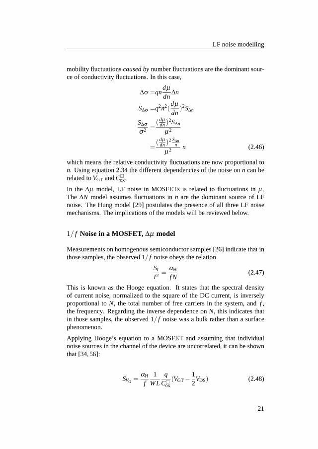
LF noise modelling
mobility fluctuations caused by number fluctuations are the dominant sour-ce of conductivity fluctuations. In this case,
∆σ =qndµdn
∆n
S∆σ =q2n2(dµdn
)2S∆n
S∆σσ2 =
( dµdn )2S∆n
µ2
=( dµ
dn )2 S∆nn
µ2 n (2.46)
which means the relative conductivity fluctuations are now proportional ton. Using equation 2.34 the different dependencies of the noise on n can berelated to VGT and C
ox.
In the ∆µ model, LF noise in MOSFETs is related to fluctuations in µ .The ∆N model assumes fluctuations in n are the dominant source of LFnoise. The Hung model [29] postulates the presence of all three LF noisemechanisms. The implications of the models will be reviewed below.
1/ f Noise in a MOSFET, ∆µ model
Measurements on homogenous semiconductor samples [26] indicate that inthose samples, the observed 1/ f noise obeys the relation
SI
I2 =αH
f N(2.47)
This is known as the Hooge equation. It states that the spectral densityof current noise, normalized to the square of the DC current, is inverselyproportional to N, the total number of free carriers in the system, and f ,the frequency. Regarding the inverse dependence on N, this indicates thatin those samples, the observed 1/ f noise was a bulk rather than a surfacephenomenon.
Applying Hooge’s equation to a MOSFET and assuming that individualnoise sources in the channel of the device are uncorrelated, it can be shownthat [34, 56]:
SVG =αH
f1
WLq
Cox
(VGT − 12
VDS) (2.48)
21

2. BACKGROUND
In the linear region with low VDS this reduces to:
SVG =αH
f1
WLqVGT
Cox
(2.49)
and in saturation (substituting VGT in the place of VDS as the voltage overthe channel) it becomes:
SVG =αH
f1
WLqVGT
2Cox
(2.50)
The ∆µ model predicts that SVG should scale with the inverse of the devi-ce area, should be linearly dependent on VGT and inversely dependent onC
ox. p-Channel devices are often reported to exhibit 1/ f noise behaviour inaccordance with the ∆µ model [10, 56].
Substituting
VGT =
√2IDL
W µCox
(2.51)
it may be concluded that in saturation, with ID kept constant, the gate-referred noise is proportional to W−3/2L−1/2.
Given a measured SVG at a particular frequency, it is always possible to cal-culate αH if the parameters of the device are known. This does not have toimply a ∆µ origin of the LF noise (although αH is often primarily associa-ted with the ∆µ model), but can be useful simply as an empirical measure ofthe LF noise normalized to the drain current, the frequency and the numberof free carriers in the device.
1/ f Noise in a MOSFET, ∆N model
Number fluctuations in a MOSFET can also cause low frequency noise.Number fluctuations are caused by trapping and detrapping of mobile car-riers in traps at the interface or in the oxide. The area, bias and C
ox depen-dency predicted by this so-called ∆N model will be reviewed. In the linearregion,
SVG =SQSS
C2ox W 2L2
=q2S∆N
C2ox W 2L2
(2.52)
22
LF noise modelling
SQSS Is the spectrum of surface state charge fluctuations. Assuming thatthe noise sources in the device are uncorrelated, S∆N = S
∆NWL may besubstituted to derive:
SVG =q2
C2ox WL
S∆N
(2.53)
The spectrum of number fluctuations per unit area (S∆N) is independent
of the size of the device if the device is uniform. This means, that likethe ∆µ model, the ∆N model predicts that the gate referred PSD of noiseshould scale with the inverse of the device area. To a reasonable approxi-mation, S
∆N is not bias dependent. This is because the trapping processis rate-limited by the number of available traps, not the number of availa-ble free carriers. Hence, the ∆N model predicts that the gate-referred noisePSD should be independent of VGT and proportional to C−2
ox . n-ChannelMOSFETs are often seen to exhibit 1/ f noise behaviour in accordance withthe ∆N model.
Equation 2.53 is equally valid in the linear region and in saturation [18].Since SVG is not dependent on VGT, eq. 2.53 gives the correct scaling re-gardless of whether VGT or ID is kept constant.
McWhorter’s ∆N model
So far, the area and bias dependence of ∆N fluctuations has been addressedwithout discussing what the shape of the spectrum described by S
∆N is.McWhorter was the first to show that a trapping/detrapping process canlead to a 1/ f type spectrum [51]. His derivation will be briefly summarizedhere.
A single trap gives rise to a Lorentzian PSD, as shown in section 2.3 above.If a MOSFET contains a ‘large’ number of such traps, and these traps donot interact, their PSD’s may be added. If the traps all generate an RTS withthe same amplitude, and their time constants are exponentially distributed,the summation of their PSD’s will have a 1/ f shape. This is shown infig. 2.4. An exponential distribution of time constants may result froma uniform distribution of the distance from the channel to the traps in theoxide, if tunnelling is the mechanism by which charge carriers from thechannel interact with the traps [23].
There are some issues regarding the McWhorter model that deserve menti-on:
23

2. BACKGROUND
100
101
102
103
104
100
101
102
103
104
105
106
PS
D [A
rbitr
ary
scal
e]
Frequency [Hz]→
← 1/f
Lorentzian spectra →
Figure 2.4: Addition of Lorentzian spectra results in a 1/ f spectrum
• The McWhorter model describes sufficient conditions for the emer-gence of a 1/ f spectrum, not necessary conditions. For example,in [53], far less stringent conditions for the emergence of a 1/ f spec-trum from RTS noise are derived.
• If the RTS time constants are solely due to the distance of the trap inthe oxide, one would expect a low frequency cutoff for the 1/ f noisein devices with very thin oxides. Such a cutoff has not been observed.
• The McWhorter model was derived in a time when devices were ‘lar-ge’, and the postulate of a ‘large’ number of traps seemed reasonable.In very small area devices, (eg Brederlow [9] measures 30..300 trapsper µm2 in a 0.25 µm process) averaging does not occur and the Mc-Whorter model is not directly applicable.
• Measurements of RTS noise on small devices indicate that traps mayin fact interact with one another. [33].
Hung 1/ f noise model
The Hung 1/ f noise model [28, 29] is often used in circuit simulators. Itis based on a model of number fluctuations and correlated mobility fluctu-ations. With suitable parameters, it is able to achieve excellent correlationwith measured results [71]. The basic form of the Hung 1/ f model for
24

LF noise modelling
small VDS is given in [29]:
SVG ∝kTq2
γ fWLC2ox
(1+αµN)2 (2.54)
This equation expresses that the capture of a mobile charge carrier causes acorrelated fluctuation in mobility due to Coulomb scattering at the interfa-ce. Depending on the strength of the coupling coefficient α , it predicts theexistence of three regions2.
For αµN << 1, the model reduces to the simple ∆N model, predictingSVG to be independent on VGT, and C−2
ox .
For αµN ≈ 1, the model states
SVG ∝kTq2N
WLC2ox
=kTqVGT
WLCox
(2.55)
Which is equivalent to the ∆µ model, predicting a dependency of SVG onVGT C−1
ox .
The third area of the Hung model is for αµN >> 1, this is when mobilityfluctuations resulting from number fluctuations dominate. In this area, SVG
is proportional to V 2GT.
RTS noise in MOSFETs
In MOSFETs with a small number of free carriers, RTS noise rather than1/ f noise is observed. A useful review of the history of RTS observationsin MOSFETs is given in [33]. Assuming that:
• 1/ f Noise is caused by mobility fluctuations with a given αH,• The RTS noise is pure ∆N, i.e. there is no mobility fluctuation as a
result of the Coulomb scattering from trapping,• The RTS noise is visible if the amplitude of the RTS is larger than the
RMS value of the 1/ f noise in the observation bandwidth,
a simple condition can be derived [35] for the visibility of the RTS noise:
N ≤ 1αH ln( fm(τc + τe))
(2.56)
αH is the Hooge empirical 1/ f noise factor, fm is the bandwidth of themeasurement setup, and τe and τc are the parameters of the RTS.
2Note that this α is not the same as αH used in the context of the ∆µ LF noise model.
25

2. BACKGROUND
Noise sourceScaling
W and L Cox (∝ 1/tox) VGT
Thermal W−1L C−1ox VGT (lin) V−1
GT (sat)
∆µ W−1L−1 C−1ox VGT
∆N W−1L−1 C−2ox V 0
GT
Correlated ∆N and ∆µ W−1L−1 C0ox V 2
GT
Table 2.1: Overview of LF noise models
The visibility of the RTS improves with smaller αH, smaller measurementbandwidth and higher RTS corner frequency.
Overview
The important scaling properties of the different models are given in table2.1. W and L scaling is given, as is the C
ox and VGT dependency. Scalingrules for the 1/ f corner frequency fc can be derived if so desired. Notethat whereas thermal noise is always present in the channel of a MOSFET,and SID,th is non-zero for any VDS, this is not the case for LF noise. Aspredicted by the different noise models, SID = 0 when ID = 0. Regardingthe ∆µ model, this is immediately obvious from equation 2.47. Regardingthe ∆N model, SVG does not go to 0 for VDS =0 (equation 2.53) but gm does,thereby reducing SID to 0 for VDS =0.
2.6 The future of LF noise in MOSFETs
CMOS downscaling is expected to continue for a number of process gene-rations [30]. A change in gate dielectric from SiO2 to a so-called ‘High-κ’dielectric is expected by 2006 or 2007 [30]. This is expected to aggravatetrapping and associated LF noise problems, as high-κ gate dielectrics arereported to have interface state densities one or two orders of magnitudehigher than SiO2 [69].
To investigate the effect of downsizing MOSFETs on their LF noise, a nextprocess generation is modelled by a shrink factor s. We discuss how this
26

The future of LF noise in MOSFETs
Current process generation Next process generation
tox tox/s
Cox s C
ox
VDD VDD/s
VGT VGT
Table 2.2: Simple model for CMOS scaling
affects 1/ f noise. The upcoming change to high-κ gate dielectrics shouldbe considered in isolation.
The main difference between one process generation and the next (table2.2) is the decreasing tox, leading to an increase in C
ox. To prevent oxidebreakdown, this mandates an equivalent decrease of VDD. VT scales downfrom one process generation to the next, but analog CMOS design over thepast few process generations has shown that VGT in typical analog circuitsdoes not change much from one generation to the next [2], so VGT is model-led as constant. To evaluate how the 1/ f noise changes from one processgeneration to the next, boundary conditions have to be selected. Several canbe chosen, and some are mutually exclusive. Some possibilities are:
• Keep σVT , the spread in VT, constant. This is realistic in the lightof the observation that VGT does not change much from one processgeneration to the next. Using the relation for the spread in VT:
σVT =AVT√WL
(2.57)
where AVT is a constant proportional to tox, this means WL will haveto decrease by a factor s2 from one process generation to the next.
• Keep Atot, the total area, constant. This means WL will remain thesame from one process generation to the next. Keeping the total areaconstant is equivalent to keeping the relative spread in VT; σVT/VDD
constant.• Keep SNRth, the signal-to-thermal noise-ratio, constant. At con-
stant VT, keeping SNRth constant means keeping SVth constant. Fromequation 2.40, this means L/W should increase by s from one processgeneration to the next.
• Keep PDD, the supply power, constant. Since VDD is dropping bya factor s, this means increasing ID by a factor s. Making use of
27

2. BACKGROUND
PDD constant SNRth constant
Atot constant W 1 s−1/2
L 1 s1/2
WL 1 1
SVG (C0ox/C−1
ox /C−2ox ) 1/s−1/s−2 1/s−1/s−2
fc (C0ox/C−1
ox /C−2ox ) s/1/s−1 1/s−1/s−2
σVT constant W s−1 s−3/2
L s−1 s−1/2
WL s−2 s−2
SVG (C0ox/C−1
ox /C−2ox ) s2/s/1 s2/s/1
fc (C0ox/C−1
ox /C−2ox ) s3/s2/s s2/s/1
Table 2.3: The future of 1/ f noise. Downscaling by factor s under givenconstraints. C0
ox/C−1ox /C−2
ox refers to ‘correlated ∆N and ∆µ’, ∆µ and ∆N1/ f noise models respectively
equation 2.32, this means keeping W/L constant from one processgeneration to the next.
Either σVT or Atot can be kept constant, in combination with either PDD orSNRth. This leads to the scaling rules for W and L as given in table 2.3.It is up to the designer to decide which of the four possibilities is mostapplicable to the situation in question. SVG Is probably the fairest indicatorof whether the 1/ f noise is becoming more or less in absolute terms whilefc, the 1/ f noise corner frequency, indicates the relative importance of 1/ fnoise compared to thermal noise.
The most realistic approach to scaling is to keep (a) SNRth and (b) σVT
constant (the lower right hand corner in table 2.3). In this way, we are (a)comparing the LF noise to the thermal noise, and (b) keeping the matchingproperties of the circuit the same. Under these conditions, fc will increasefor the correlated ∆N and ∆µ model and the ∆µ model, and remain unchan-ged for the ∆N model. Other boundary conditions may be chosen to makethis evaluation (eg. in [71] a simulation-based rather than an analytical ap-proach is used), but similar conclusions result.
28

Conclusion
2.7 Conclusion
In this chapter, we have reviewed frequency and time domain analysis ofstochastic signals, and common LF noise models for MOSFETs and theirimplications are discussed.
The dependence of the relative conductivity fluctuation (S∆σ /σ2) on thefree carrier concentration n is derived. This is the basis on which the diffe-rent LF noise models for MOSFETs, namely the ∆µ , ∆N and the correlated∆µ and ∆N models are distinguished.
It is expected that LF noise in small-area devices will continue to be RTS-dominated. For future CMOS process generations, the relative importanceof LF noise compared to thermal noise is not expected to decrease. (table2.3). The expected change in future CMOS processes from SiO2 to a high-κ gate dielectric is expected to increase LF noise problems as trap densitiesin high-κ gate dielectrics are much higher than in SiO2.
29


Chapter 3
Measurement of LF noise underlarge signal excitation
3.1 Introduction
In our study of LF noise under Large Signal Excitation (LSE) numerousmeasurements of MOSFET LF noise behaviour under LSE have been per-formed. In this chapter, the most important experiments and their resultswill be presented. First, LF noise measures will be briefly discussed so thatthese can be used to describe the results of the experiments. We reviewthe published data on the subject. Next, the most important measurementresults are presented. Factors that influence LF noise are presented; mostimportantly: what is the waveform and amplitude of the large signal thatthe device is subjected to and to what terminal of the device is it applied.Device factors that influence noise and noise under LSE will be described;such as process factors (in particular: tox, device size, and device polarity (nor p-channel). There is a significant difference between measurements onsingle selected ‘golden samples’, which exhibit spectacular behaviour whensubjected to LSE, and ‘real-world’ performance of randomly selected setsof devices. Though both types of measurement are valuable, it is importantto be aware of this distinction. To investigate spread of LF noise and LFnoise under LSE, measurements of LF noise under LSE on large sets ofunselected devices are presented. Finally, we will summarize.
31

3. MEASUREMENT OF LF NOISE UNDER LARGE SIGNAL EXCITATION
101
102
103
104
10−2
10−1
100
101
f−1
Frequency [Hz]
PS
D [W
/Hz]
Figure 3.1: 1/ f Spectrum
3.2 Measures for LF noise
LF noise may be examined in the frequency domain and in the time domain.The two, though fundamentally related, give quite different insights in noisebehaviour. Both are useful.
LF noise in the frequency domain
Noise can be characterized by a plot of its Power Spectral Density (PSD).The PSD gives the noise power per unit of bandwidth as a function of fre-quency. The units of the PSD are W/Hz. This is often plotted on a loga-rithmic scale by converting to decibels, using a suitable reference power.In many practical experiments, the noise voltage or the noise current ratherthan the noise power is measured. A constant load impedance is assumed,and the relative noise power is simply expressed as V2/Hz, or as A2/Hz.Again, decibels are commonly used, leading to the oft-seen dBV2/Hz (whe-re the 0 dB reference is 1V2/Hz) or dBA2/Hz (where the 0 dB reference is1 A2/Hz).
1/ f Noise derives its name from the 1/ f shape of its PSD as in fig. 3.1.
S1/f =Kf
f γ (3.1)
32

Measures for LF noise
101
102
103
104
10−2
10−1
100
101
f−2
Frequency [Hz]
PS
D [W
/Hz]
↑ f0,RTS
Figure 3.2: Spectrum of a Lorentzian signal
where Kf is a constant and γ is close to 1. A common limit for noise to beclassified as 1/ f noise is 0.9 < γ < 1.1 [27]. When examining LF noisein small MOSFETs, a more complex spectrum with γ frequency dependentand varying between 0 and 2 is often observed. This type of spectrum isusually considered to consist of a summation of various so-called ‘Lorent-zian’ spectra. A single Lorentzian has the following PSD:
SLorentzian =Kl
1+( f/ f0)2 (3.2)
In which Kl is a constant and f0 is the corner frequency of the Lorentzi-an. Below f0, the PSD of the Lorentzian is flat; above f0 it it has a f−2
characteristic. A Lorentzian PSD is given in fig. 3.2.
When studying LF noise, it is often desired to compare the LF noise in thesteady state to the LF noise under LSE. Whereas the steady state spectrumwill generally have a reasonably regular form similar to that in fig. 3.1or fig. 3.2, the measured noise spectrum under large signal excitation ismore complex: Not only will it contain the LF noise of interest, but alsoharmonics of the excitation signal and associated modulated LF spectra. Inmany cases, these modulated spectra are not of primary interest, as it is onlydesired to quantify whether the large signal excitation has changed the LFnoise, and if so, in which direction and by how much.
33

3. MEASUREMENT OF LF NOISE UNDER LARGE SIGNAL EXCITATION
101
102
103
104
105
Frequency [Hz]
PS
D [5
dB
/div
]Steady StateLSE
Figure 3.3: Spot noise measurement is suitable if PSD’s to be comparedhave the same slope
Spot noise measurement
The difference between two spectra may be quantified in terms of the dis-tance between them at a particular frequency. The ‘spot’ frequency at whichthe noise measurement is made should be given, but the spot noise measure-ment is only really suitable if the PSDs have the same slope for a significantfrequency range as, for example, in figure 3.3, so this is often not very criti-cal. A spot frequency should be selected that is free from spurs (undesiredharmonic components in the PSD). The most obvious spur frequencies inthe lab that should be avoided are multiples of 50 Hz; several are visible infig. 3.3. The spot noise measurement is simple and insightful and is usefulfor rapid noise estimates in the lab. However, being a measurement at a sin-gle frequency, the spot noise measurement gives only limited information,and it gives no information on the shape of the spectrum at all.
Integrated noise measurement
When the PSD’s to be compared are not parallel, for example in fig. 3.4in which a significant Lorentzian component is seen in the steady statemeasurement, the spot noise measurement will give very variable resultsdepending on the frequency at which it is applied, and it is no longer a
34

Measures for LF noise
101
102
103
104
Frequency [Hz]
PS
D [5
dB
/div
]
n−channelW/L=0.2/0.18 µmtox
=4 nmV
T=0.35 V
Steady StateLSE
Figure 3.4: Steady state and LSE noise
representative estimate of the difference between the two PSD’s. In suchcases, a better approach is to integrate the noise over some bandwidth andcompare the integrated noise of the PSD’s. Care should again be taken toavoid spurs in the integration interval, and to give the best measure of noise,the integration interval should be as wide as reasonable.
Systematic effects and ‘net noise reduction’
In some experiments, when comparing LF noise measurements in the steadystate to those under LSE, a correction needs to be made for the fact thatthe device is ‘off’ for some of the time when it is subjected to LSE. Onesuch example will be treated here. In this experiment [65], the device isperiodically turned ‘off’ and ‘on’ in an abrupt manner and with a 50% dutycycle. The two signals of which the PSD’s will be compared are given infig. 3.5.
If the steady-state noise is described by
n(t) (3.3)
the modulated signal can be described by
C(t) = n(t)B(t) (3.4)
35

3. MEASUREMENT OF LF NOISE UNDER LARGE SIGNAL EXCITATION
a) steady state bias
b) LSE.
t0 T/4 T/2- /4T- /2T
n(t)
C(t)
Figure 3.5: Systematic noise decrease under LSE: comparing equation 3.3and 3.4
Where B(t) is a square wave varying between 0 and 1, and C(t) is cyclo-stationary. Its PSD can be calculated by first calculating its cyclostationaryautocorrelation function RCC(t, t + τ), ‘stationarizing’ it by averaging theautocorrelation function over one period [16], (this discards phase informa-tion which is not important for the PSD), and finally Fourier transformingit to obtain the PSD.
RCC(t, t + τ) = E[n(t)B(t)×n(t + τ)B(t + τ)] (3.5)
Since n(t) and B(t) are uncorrelated, this can be rewritten as:
RCC(t, t + τ) =E[n(t)n(t + τ)×B(t)B(t + τ)]=E[n(t)n(t + τ)]×E[B(t)B(t + τ)]=Rnn(t, t + τ)×RBB(t, t + τ) (3.6)
Rnn(t, t +τ) is the autocorrelation function of the noise. If the noise is stati-onary, Rnn(t, t + τ) = Rnn(τ). RBB(t, t + τ) is not stationary (it is a functionof both t and τ) and needs to be stationarized first. Referring to fig. 3.5, wefirst write:
RBB(t, t + τ) =1(t + τ +T/4)×1(−(t + τ)+T/4) for | t |< T/4
=0 for T/4 <| t |< T/2 (3.7)
In this equation, t is the time at which the autocorrelation function is cal-culated, and τ is the time offset that describes the autocorrelation functionat that time. To stationarize this signal, the autocorrelation function is aver-aged over one cycle. The stationarized autocorrelation function is denoted
36

Measures for LF noise
by RBBs.
RBBs(τ) =1T
∫ T/2
−T/2RBB(t, t + τ)dt
=12
1(T2
+ τ)+τT
1(T2
+ τ)− 2τT
1(τ)
−12
1(−T2
+ τ)+τT
1(−T2
+ τ) (3.8)
This is a triangular function of τ with height 0.5 and width (−T/2..T/2).The Fourier transform can now be performed. The autocorrelation functionis a multiplication of
RCCs(τ) = Rnn(τ) RBBs(τ) (3.9)
This will give a convolution of the PSD of the noise and the PSD of thesquare wave in the frequency domain. The relative amplitude of the base-band alias and the first alias is most interesting. The baseband alias willhave a power of 1/4 relative to the steady state case and the nth alias willhave an power of 2/(nπ)2 relative to the steady state case. In the PSD, thisis -6.0 dB for the baseband alias and -6.9 dB for the first alias. The 3rd
alias will be at -16.5 dB. This is illustrated in fig. 3.6. Assuming that thebaseband alias of the PSD can be validly interpreted if the first alias is somedistance below the baseband alias of the PSD, the maximum frequency upto which the baseband alias can be correctly interpreted can be derived ifwe assume a 1/ f shape of the PSD:
fex
fmax= 1+
41
2π2 10
d10 (3.10)
In this equation fmax is the highest frequency for which the baseband aliascan be validly interpreted, fex is the frequency of excitation, and d is thedistance in dB that is required between the baseband alias and the first alias.If a 3 dB distance between the baseband and the first alias is required, thebaseband alias is free from aliasing up to a maximum frequency of 0.38 fex,as can be seen in fig. 3.6.
LF noise in the time domain
In the time domain, the most obvious way to characterize a stochastic sig-nal is by its autocorrelation function. If the signal is cyclostationary, it can
37

3. MEASUREMENT OF LF NOISE UNDER LARGE SIGNAL EXCITATION
3 dB (’d ’)
Baseband Alias(−6.0 dB)
1st Alias(−6.9 dB)
3rd Alias(−16.5 dB)f
ex0.38 fex
Frequency →
PS
D [5
dB
/div
]
Figure 3.6: 1st Alias limits measurement of baseband alias
be stationarized first and the PSD can then be calculated using the stationa-rized autocorrelation function. However, stationarizing the autocorrelationfunction (as is done when a PSD is examined) is not always desirable. Forexample, in switched capacitor circuits, a noisy transistor that is subjectedto a large (on-off) bias transient is used to take a sample of a signal. Thecyclostationarity of the noise is relevant because the noise of the transistorat a particular time in the period is relevant, and stationarizing the noiseby averaging the statistical parameters over the whole period is not approp-riate [42]. For these sorts of situations a measure of noise at a particulartime following a bias transient will be defined. This will be called the time-dependent noise.
Time-dependent noise
If the period of large-signal excitation is T , the time-dependent noise isdefined as the series of samples taken at time instants nT + toffset. n is thenumber of the period (n = 1..nmax), and toffset is the time offset in the periodrelative to the start of the period (fig. 3.7). The noise being subjected to LSEis cyclostationary so the time-dependent noise series is stationary, but itsstatistical parameters (including its mean and variance) may be dependenton toffset. Extracting the time-dependent noise is equivalent to subsamplingthe original noise with a sampling frequency of fex, so the variance of the
38

Review of published measurement results
Figure 3.7: Time-dependent noise
time-dependent noise is equal to the integrated noise PSD from 1/nmaxT tothe bandwidth of the noise at a particular point in the period. Referring tofig. 3.7, if toffset > T/2 the time-dependent noise will be 0.
The time-dependent noise is an appropriate noise measure in systems wherethe use of the noisy device is synchronous with the large signal that thedevice is subjected to. Switched-capacitor circuits are an obvious example.In these systems, the variance of the time-dependent noise is of primaryimportance. The average value of the time dependent noise may also be afunction of toffset. This is important if the device is used at different timesfollowing a bias transient. A good example of this is the correlated doublesampling circuit discussed in section 5.3
3.3 Review of published measurement results
In this section, previously published LF noise measurements under LSEare presented. The first observation of the fact that LF device behaviourdepends on the bias history as well as on the bias state of the MOSFET datesfrom around 1985, however this was not published until much later [70].First published measurement results are from 1991 [7]; later we presentedmore extensive measurement results on large-area HEF 4007 MOSFETs[65].
In [70], Eric Swanson discusses the design of the Crystal SemiconductorCS5016, a 50 kHz, 16 bit AD converter, which took place around 1985. Aslow tail in a comparator offset voltage was observed following a compara-tor overdrive. Measurements were done on a 3 µm process from Orbit Se-miconductor. It was also found (‘5x worse’) in 3N169 discrete MOSFETs.
39

3. MEASUREMENT OF LF NOISE UNDER LARGE SIGNAL EXCITATION
The problem was solved by periodically pulling the source of the compa-rator transistors up to VDD. A few ns of such ‘flush time’ was found to besufficient to cure the effect, which was attributed to slow trapping and de-trapping in the oxide. This is the first mention of the use of LSE to combatlow-frequency effects in MOSFETs. No mention is made of improved LFnoise characteristics of the transistors involved, though it is entirely possiblethat this happened as a side effect.
In [6,7], Bloom and Nemirovsky present an experimental setup for and me-asurement results of LF noise in Si-MOSFETs subjected to LSE at the gate.Large MOSFETs were used (100/8 and 80/8 µm from a CMOS processfrom ‘Technion’ in Israel), biased in the linear region and in saturation. Theswitching frequency was 600 Hz, and noise measurements were done bet-ween 1 and 100 Hz. A noise power reduction by a factor 3 was observed at1 Hz. The effect was found to be independent of duty cycle for duty cyclesbetween 25% and 88%. Various other transistors were measured, and a noi-se power reduction by a factor between 1.2 and 3.7 was observed at 1 Hz.The observed noise power reduction showed little sensitivity to the positionof the sampling pulse within the ‘on’ period.
In [14], more noise measurements under LSE are presented by Dierickx andSimoen. A noise reduction was found ‘Systematically on large-area devi-ces’. It was observed that when subjected to LSE, ‘RTS noise disappears’,and the suggestion is made that subjecting the device to LSE could be ‘apossibility to separate the contributions of different sources of 1/ f noise inMOSFETs.’ Experimental results are presented on 3.5/3.5 µm MOSFETsfrom a 3 µm process from IMEC in Belgium. tox = 60 nm, And the deviceshave no LDD. For four n-channel devices, an average noise decrease by afactor 8.4 at 1 Hz was found. For four p-channel devices, this was a fac-tor 3.9. The devices were in saturation. RTS noise was measured on four0.4/0.8 µm MOSFETs with a total of 8 traps. This measurement was donein the linear region. In steady state, τe was found to be independent of VGS,while τc decreased with increasing VGS. Under LSE, the same behaviourwas observed, except for very low VGS, where τe was seen to decrease withdecreasing VGS. This is associated with accumulation.
In [20], Gierkink shows that the phase noise of a discrete ring oscillatorequipped with HEF 4007 MOSFETs depends on the amplitude of oscilla-tion. Varying the amplitude of oscillation varies almost everything in theoscillator, so measurements of upconversion were made using a pilot-toneto calibrate the measurement setup. The remaining LF noise change aftercalibration is attributed to the LF noise change of the devices. An 8 dB
40

Review of published measurement results
VDD
VC
VSS
R RD D
Cascode transistors
DUT (2x)
Signal generator
Differential preamp
Oscilloscope SpectrumAnalyser
Figure 3.8: Noise measurement setup to measure LF noise in steady stateand under LSE
reduction in LF noise is noted. This is reported for one sample, thoughmeasurements on devices from different manufacturers were performed.
In [65], we present measurements of HEF 4007 MOSFETs. A noise reduc-tion due to LSE of 6. . . 8 dB was systematically found in these devices. Thedevices are not specified for analog applications, and the process used is notspecified either. Hence, exact device size and oxide thickness is not known.It is clear however that these devices are large-area (input capacitance of ann-channel device is typically 5.5 pF) and that they have a thick gate oxide(VT = 1.9 V, and the gate oxide breakdown voltage is > 18 V).
Figure 3.8 shows the measurement setup used to measure LF noise underLSE as used in [65]. The cascode transistors serve to keep VDS constantduring the measurement, and the differential nature of the circuit (the twoDUTs are driven in-phase) helps make this setup immune to external noisesources such as supply noise and noise from the signal generator. One ofthe two resistors RD is variable to adjust for mismatch between the twoDUTs. The LSE applied to the gates of the device is typically a 50% squarewave with the high level of the square wave identical to the bias level of thesteady state measurement; in this way the steady state measurement may bedirectly compared to the LSE measurement; bias dependency of LF noisedoes not influence the measurement.
A typical measurement is shown in fig. 3.9. At low frequencies, 6 dBbetween the LSE and the steady state curve is expected on mathematical
41

3. MEASUREMENT OF LF NOISE UNDER LARGE SIGNAL EXCITATION
101
102
103
104
105
Frequency [Hz]
PS
D [5
dB/d
iv]
n−channelV
T=1.9 V , I
D,ON=140 µA
VGS
=0 V/2.5 V,10 kHz, 50%
Steady StateLSE
Figure 3.9: LF noise measurement on HEF 4007 device
grounds; the observed difference is 14 dB of which 8 dB is attributed to thedecrease of LF noise due to LSE. Several devices were measured and an LFnoise decrease of this magnitude was consistently observed.
A measurement was also performed in which the frequency of excitationwas varied (fig. 3.10). The measurement results show that the frequencyof excitation is not important for the LF noise as long as the frequency ofexcitation is high compared to the frequency of LF noise.
Finally, the ‘off’ voltage of the switching waveform was varied. It wasobserved that the devices needed to be cycled well below threshold before asignificant noise reduction was seen. These results are plotted in fig. 3.11.
3.4 Large signal bias factors and their influence on LFnoise
Introduction
In this section experimental results are presented that show how MOSFETLF noise under large signal excitation is influenced by different parametersof the large signal waveform. We will review the dependence of LF noiseunder LSE on:
42

Large signal bias factors and their influence on LF noise
101
102
103
104
105
DC
100 Hz
1 kHz
10 kHz
100 kHz
1 MHz
Frequency [Hz]
PS
D [5
dB
/div
]
n−channelV
T=1.9 V , I
D,ON=140 µA
VGS
=0 V/2.5 V, 50%
Figure 3.10: LF noise under LSE as a function of the frequency of excitation
101
102
103
104
105
Frequency [Hz]
PS
D [5
dB
/div
]
n−channel, VT=1.9 V
ID
=140 µA, VGS,ON
=2.5 V
Steady StateV
off=1.5 V
Voff
=1 VV
off=0.5 V
Voff
=0 VV
off=−0.5 V
Figure 3.11: Device needs to be switched to well below threshold for noisereduction
43

3. MEASUREMENT OF LF NOISE UNDER LARGE SIGNAL EXCITATION
• The circuit configuration,• The duty cycle,• How far the device is turned ‘off’.
Circuit configuration
In a circuit, a MOSFET may encounter LSE in several ways. Dependingon the design of the circuit, either VG or VS may be periodically time va-riant. VD is not critical to the behaviour of the MOSFET as long as it ishigh enough to keep the device in saturation, and VB is not always availableas a separate terminal, or it may be shared between several devices. It istherefore relevant to examine the effect of periodic LSE at the gate and atthe source. In particular, we want to find out whether there is a significantdifference between these two modes of excitation as far as the LF noiseperformance of the MOSFET is concerned.
Comparative measurement method
To compare the effect of LSE at the gate and LSE at the source, the deviceis turned off periodically by either:
• varying VG periodically between an ‘on’ value and an ‘off’ value whi-le keeping VS at a constant voltage, or
• varying VS periodically between a low ‘on’ value and a high ‘off’value, while keeping VG at a constant voltage.
The LF noise in each of these situations is compared to the LF noise in stea-dy state. The three states to be compared are shown in fig. 3.12. To makethe steady state measurements directly comparable to the LSE measure-ments, the ‘on’ bias state in each of the three situations is made identical:the current is kept at 20 µA exactly. Depending on the W/L of the device,this results in a device that is more or less strongly inverted.
In each of the three situations, the noise at the source terminal of the devi-ce is measured using the measurement setup of fig. 3.13. Details of eachoperating condition are given in table 3.1. The first half of the setup is fullydifferential; i.e. all parts including the DUTs are duplicated and the pream-plifier is differential. The large periodic signal is common-mode, and istherefore attenuated by the common mode rejection ratio of the differentialdifference amplifier. This reduces the dynamic range requirements of theremainder of the measurement setup. Working differentially also helps to
44

Large signal bias factors and their influence on LF noise
Figure 3.12: Comparison of three different bias conditions: (a) Steady state,(b) LSE at gate, (c) LSE at source.
suppress interference from the measurement setup and the different voltagesources such as Vext. The device noise of the two DUTs is uncorrelated andtheir noise powers therefore add at the output.
The operating conditions of the different sources and switches is given intable 3.1. Note that switches B and C are also operated for the constant-biasmeasurement to make the operating conditions of the amplifiers as closeas possible to the switched gate or switched source case. In this way, thepossibility that the measurement results are caused by some transient effectin the amplifier can be precluded since all the measurements drive the am-plifier in the same way. Vext is an external voltage approximately equal tothe common-mode input voltage of the differential amplifier, that preventsthe amplifier from saturating when the device is disconnected from its input(when switch B is open). It is also used to prevent VS from changing whenVG is varied.
Since ID is determined by the gate-source voltage VGS, the gate-referredvoltage noise (which is of interest) is equal to the source-referred volta-ge noise (which is measured). The steady-state measurement is repeatedtwice for each device to check whether the measurement is consistent andreproducible. To further preclude possible effects of drift and temperaturedifferences, the steady state and the switched measurements on each deviceare done in an alternate fashion.
For the LSE measurements, the device is turned on and off with a frequencyof 100 Hz. The noise is sampled for 5 µs immediately following the turn-on
45

3. MEASUREMENT OF LF NOISE UNDER LARGE SIGNAL EXCITATION
I =20 A
DUT
Differential
50
DigitalOscilloscope
Differentialdifferenceamplifier(AD8130)
100xPreamplifier(BW=40 MHz)
SW'A'
SW'B'
SW'C'
V
V =3.3 V V =2 V
V
G
D Soff
ext
S
Figure 3.13: Measurement setup for LSE at gate and LSE at source
Steady state LSE at gate LSE at source
VG 2 V DC 0 V/2 V 50%100 Hz
2 V DC
SW ‘A’ OPEN OPEN 50% 100 Hz
SW ‘B’ 50 % 100 Hz CLOSED Out of phasewith SW ‘A’
SW ‘C’ Out of phasewith SW ‘B’
CLOSED whenVG = 0 V
In phase withSW ‘A’
Table 3.1: Operating conditions for the measurement setup for steady state,LSE at gate and LSE at source
46

Large signal bias factors and their influence on LF noise
Steady state LSE at gate LSE at source
VG 2.0 V (DC) Square wave, 0V / 2 V, 50%,100 Hz
2.0 V (DC)
VS Determined byID
Vext / determinedby ID
Square wave, 2.0V / determinedby ID, 50%, 100Hz
VD 3.3 V (DC) 3.3 V (DC) 3.3 V (DC)
ID 20 µA perdevice
0 / 20 µA perdevice
0 / 20 µA perdevice
Table 3.2: Bias conditions for Steady state bias conditions, LSE at the gateand LSE at the source.
transient. The sampling frequency is 200 MHz, giving 1000 data points foreach turn-on transient. After storage of the data (this takes approximately1 second), the experiment is repeated. The experiment is repeated a totalof 500 times for each bias condition (steady state, LSE at gate, LSE atsource) for each sample. We want to determine the time-dependent noise(see page 38). To this end, the time-domain records are first passed througha lowpass filter with a cutoff frequency of 4 MHz to improve the LF noiseto broadband noise ratio. After that, a sample is taken of the time domaindata 0.5 µs after the turn-on transient. The variance of these 500 samplesis an empirical measure for the LF noise in a frequency range up to about0.5 Hz in all three bias conditions.
Measurement results
Measurements in all three bias conditions were carried out on a set of42 n-channel devices from one wafer. The devices are from an industri-al 0.35 µm process. Several different device sizes were available, with aW/L ratio of 0.8/0.35, 1.025/0.475, 1.125/0.525, 1.25/0.575, 0.5/0.35and 5/0.35 µm. To assign equal weight to the different size devices, thevariance of the time dependent noise is multiplied by the device area to nor-malize for the theoretical dependence of the LF noise on the area at constantID (see section 2.5). The bias conditions are given in table 3.2 below.
47

3. MEASUREMENT OF LF NOISE UNDER LARGE SIGNAL EXCITATION
10−6
10−5
10−4
10−3
10−2
10−6
10−5
10−4
10−3
10−2
Normalized steady state noise power [arbitrary scale]
Nor
mal
ized
LS
E n
oise
pow
er [s
ame
scal
e as
x−
axis
]n−channelV
T=0.65 V
tox
=7.5 nm
various W/LID,ON
=20 µA
LSE at GateLSE at Source
Figure 3.14: Noise under LSE at gate and LSE at source
An overview of the ‘LSE at gate’ and the ‘LSE at source’ measurementsis given in figure 3.14 below. Along the x-axis, the LF noise power in thesteady state is given, and along the y-axis, the LF noise power for LSE isgiven. Different symbols differentiate between the measurements with LSEat the gate and LSE at the source.
It is immediately apparent that the noise is very variable: the sample-to-sample spread is over 2 orders of magnitude. The noise under LSE showssimilar spread. For reference, a dotted line signifying ‘LSE noise=steadystate noise’ has been included in the figure. It can be seen that the majorityof points lie below the line; indicating that on average, LF noise decreaseswhen a device is subjected to LSE.
To investigate more closely the relation between LSE at the gate and LSEat the source, figure 3.15 was plotted. Along the x-axis the noise change forLSE at the source has been plotted. This is the LF noise under LSE at thesource divided by the steady state LF noise for the same device. A valuelarger than 1 indicates an increase in noise for the LSE case; conversely, avalue smaller than 1 indicates a decrease in noise for the LSE case. Alongthe y-axis, the same quantity is plotted for the ‘LSE at gate’ experiment.For reference, a line y = x is also included in the figure. It is immediatelyapparent the noise change for LSE at the source correlates closely with thenoise change for LSE at the gate. There is one data point that is far-removedfrom the 45o line. On further investigation, it was found that this device had
48

Large signal bias factors and their influence on LF noise
10−2
10−1
100
101
102
10−2
10−1
100
101
102
(← decrease) LSE at source noise change (increase →)
(← d
ecre
ase)
LS
E a
t gat
e no
ise
chan
ge (
incr
ease
→)
n−channelV
T=0.65 V
tox
=7.5 nm
various W/LID,ON
=20 µA
Figure 3.15: Switched Gate compared to Switched Source
a very slow RTS, with time constants of the order of the measurement-time(approx. 500 s), which influenced the measurement. A longer measurementon this device would give better results.
Conclusion
Subjecting the device to LSE at its gate and at its source is largely equivalentin terms of LF device noise.
Duty cycle
When subjecting a device to LSE, it is interesting to examine the effect ofduty cycle on the LF noise. The duty cycle is the fraction of the period thatthe device is ‘on’ and generating noise. In terms of LF noise under LSE,it is important to know whether the device needs to be turned ‘off’ for alarge percentage of the time to influence its LF noise, or whether subjectingthe device to a brief ‘off’ pulse is sufficient to influence the LF noise ofthe device. Obviously turning a device ‘off’ for a large percentage of timereduces its average output noise, but the LF output noise is examined aftercorrecting for such systematic effects.
49

3. MEASUREMENT OF LF NOISE UNDER LARGE SIGNAL EXCITATION
The first report of an LF effect under LSE [70] notes that accumulating thesurface of the device ‘for a few ns’ had significant effect, and removed theLF transient present in the device. Later, LSE experiments were carriedout [7] where the duty cycle was found to be unimportant for duty cyclesbetween 25 and 88%.
LF noise measurements were carried out [17] on p-channel devices with 10and 20 nm tox. W/L was 10/0.3 and 10/1 µm. 16 samples were measuredin total; out of these, 5 showed an LF noise decrease as the duty cycle wasdecreased; the other 11 showed the duty cycle to be largely unimportant forthe LF noise change that was observed when subjecting the device to LSE.
Next, measurements were carried out on a number of RTS-dominated de-vices [24]. These devices were n-channel MOSFETs from a 0.18 µm pro-cess1. Three devices were selected for their very visible RTS behaviour.The LF noise of these devices (integrated from 1 to 20 Hz and corrected forsystematic effects) is plotted as a function of the duty cycle in fig. 3.16. Inthis figure, one can clearly see that the behaviour of the RTS is strongly de-pendent on the duty cycle. Depending on the characteristics of the RTS, thebehaviour is very different. RTS 1 has the lowest LF noise, and it decreasesas the duty cycle decreases. RTS 2 has a maximum LF noise at a duty cycleof around 40..60%, and RTS 3 shows a maximum in LF noise for a dutycycle of 90%. Time domain measurements confirm that this behaviour is incorrespondence with the ‘effective τ’s’ of the RTS (see section 4.3). Theseare selected devices and the results may not be typical of all MOSFETs.
Conclusion
We have shown that whether or not the duty cycle of the switching wave-form is important depends on the parameters of the RTS in the device inquestion. The LF noise power behaves in accordance with the RTS parame-ters in the ‘on’ and the ‘off’ state, more detail of which is given in chapter 4.When the RTS parameters are not influenced by LSE, the duty cycle of theswitching waveform is not important; in other cases, turning the MOSFET‘off’ for a brief period of time can be sufficient to reduce the LF noise of thedevice, and turning it off for longer does not produce additional LF noisebenefits [7, 70].
1This is nominally a 0.18 µm process, but the use of phase-shift masks allows minimumdevice lengths of 0.13 µm
50

Large signal bias factors and their influence on LF noise
0 10 20 30 40 50 60 70 80 90 100
10−8
10−7
n−channel, tox
=7 nm, W/L=1/0.13 µmSelected RTS, Linear region, V
DS=40 mV
Duty Cycle [%]
LF n
oise
pow
er [a
rbitr
ary
scal
e]
n−channel, tox
=7 nm, W/L=1/0.13 µmSelected RTS, Linear region, V
DS=40 mV
n−channel, tox
=7 nm, W/L=1/0.13 µmSelected RTS, Linear region, V
DS=40 mV
RTS 1RTS 2RTS 3
Figure 3.16: LF noise as a function of duty cycle of the LSE
Waveform
Several measurements indicate that in order to influence the LF noise, theLSE the device is subjected to has to cycle the gate-source voltage to wellbelow threshold, eg. as observed in [65]. In this section, experimental datawill be presented.
Measurements were performed on p-channel devices. A number of deviceswith different oxide thickness were measured. The devices were biased insaturation and LSE was applied at the gate of the device as a 10 kHz, 50%square wave. The measurement results are given in fig. 3.17 below. Clearly,cycling the device to well below threshold is beneficial in reducing the LFnoise of the device.
Further research was done on RTS-dominated devices. Measurements in thetime domain [24] indicate that the RTS time constants change significantlyif the device is cycled to a voltage well below threshold. Measurements ofthe LF PSD (figure 3.18) of these devices are in agreement with this result.
Conclusion
In order to influence the LF noise of a MOSFET by subjecting it to LSE,the gate-source voltage needs to be cycled to ‘well below’ threshold.
51

3. MEASUREMENT OF LF NOISE UNDER LARGE SIGNAL EXCITATION
−3 −2.5 −2 −1.5 −1 −0.5 04
6
8
10
12
14
16
VT V
GS,OFF [V]
LF n
oise
red
uctio
n [d
B]
Expected 6 dB reduction
p−channel, tox
=20 nm
W/L=10/0.1 µmV
T=−2.2 V, V
DS=2.4 V
ID
=17 µA
Figure 3.17: Device needs to be cycled to well below threshold for noisereduction
−0.8 −0.6 −0.4 −0.2 0 0.2 0.4 0.610
−11
10−10
10−9
10−8
10−7
’Off’ voltage for LSE [V]
LF n
oise
pow
er (
1..2
0 H
z)
n−channel, tox
=7 nm, W/L=1/0.13 µmSelected RTS, Linear region, V
DS=40 mV
n−channel, tox
=7 nm, W/L=1/0.13 µmSelected RTS, Linear region, V
DS=40 mV
RTS 1RTS 2RTS 3
Figure 3.18: Device needs to be switched to well below threshold for noisereduction
52

Device factors and their influence on LF noise
The exact bias conditions under which a significant LF noise change is ob-served depends on the device parameters. In early literature [7, 70] it wasnoted that the device needs to be ‘cycled to accumulation’ for any signi-ficant change in the LF noise of the device to occur. For the n-channelMOSFETs used, this was done by making the gate-bulk voltage negative [7]or by pulling the source up to VDD [70]. Later measurements [65] showedthat cycling the device to accumulation was not always necessary: cyclingVGS to 0 V was sufficient. This is supported by later measurements, whereturning the device ‘off’ by pulling VS up to VG was also found to influencethe LF noise of the device.
3.5 Device factors and their influence on LF noise
Introduction
In this section, measurements are presented of LF noise under large sig-nal excitation on a variety of MOSFETs. It will be shown that p-channeldevices behave in the same way that n-channel devices do. Measurementresults are given that show how LF noise scales with device area and oxidethickness.
Device type
The difference in LF noise behaviour in steady state and under LSE wasmeasured for p-channel devices and n-channel devices. Fig. 3.19 showsthe results for a large number of p-channel devices, and fig. 3.20 shows thesame for a number of n-channel devices. We conclude that the p-channeldevices show the same trends in noise behaviour as the n-channel devices.
Device size
To investigate the dependence of LF noise on device size, measurementswere carried out on a set of devices with varying W and L. The devices arefrom a 0.18 µm process, and the measurement is carried out at constant ID.The result is plotted in fig. 3.21; LF noise power is seen to scale inverselywith the area of the device, which is in accordance with the ∆N model forLF noise (see section 2.5).
53

3. MEASUREMENT OF LF NOISE UNDER LARGE SIGNAL EXCITATION
4
6
8
10
12
14
16
Expected 6 dB noise reduction
Steady state noise level [2 dB/div]
LSE
noi
se r
educ
tion
[dB
]
p−channelW/L=10/0.3 µmID
=17 µA
tox
=2 nmtox
=3.6 nmtox
=7.5 nmtox
=10 nmtox
=20 nm
Figure 3.19: p-channel LF noise behaviour in steady state and under LSE
10−12
10−11
10−10
10−9
10−8
0
6
12
18
24
30
Expected 6 dB reduction
gate−referred steady−state noise power [V2/Hz]
LSE
noi
se r
educ
tion
[dB
]
n−channelW/L=0.2/0.18 µmtox
=4 nmV
T=0.35 V
ID
=80 µA
Figure 3.20: n-channel LF noise behaviour in steady state and under LSE
54

Spread in LF noise under large signal excitation
10−1
100
101
102
10−5
10−4
10−3
10−2
Area [µm2]
Ste
ady
stat
e LF
noi
se p
ower
[arb
itrar
y sc
ale] n−channel
tox
=7.5 nmV
T=0.65 V
ID
=20 µA
Individual devicesAverage
Figure 3.21: Noise power scales inversely with area
Technological factors
Measurements on a large number of different processes were carried out.An LF noise change under LSE was observed in almost all cases. Mea-surements were performed on: HEF 4007 devices (large devices from whatis probably a 10 µm CMOS process), 0.35 µm CMOS processes, 0.25 µmCMOS processes and 0.18 µm CMOS processes. Additionally, measure-ments were performed on a special wafer set (nominal 0.18 µm process)that was processed with varying tox. In this way, the effect of the oxidethickness can be investigated in isolation.
The results in fig. 3.22 show that the LF noise power at the drain increaseslinearly with oxide thickness. The measurement is done at constant ID. Thisis in accordance with the ∆N model (section 2.5).
Measurement results of LF noise reduction under LSE are given in fig. 3.23.The LF noise reduction is seen to increase as tox increases.
3.6 Spread in LF noise under large signal excitation
It was found that the LF noise performance of small MOSFETs (both insteady state and under LSE) shows great spread. As far as the steady stateLF noise measurements are concerned, this has been reported before in li-
55

3. MEASUREMENT OF LF NOISE UNDER LARGE SIGNAL EXCITATION
1 2 5 10 2010
−22
10−21
Gate oxide thickness [nm]
Ste
ady
Sta
te L
F n
oise
PS
D [A
2 /Hz]
p−channelW/L=10/1 µmID
=17 µA
LF noiseLinear fit (t
ox0.94)
Figure 3.22: LF noise power increases with increasing tox. Measurementsfrom special wafer set with varying oxide thickness; all devices same no-minal size.
1 2 5 10 20
4
6
8
10
12
14
16
18
20
Expected 6 dB noise reduction
Gate oxide thickness [nm]
LSE
noi
se r
educ
tion
[dB
]
p−channelW/L=10/0.3 µmID
=17 µA
Individual device
Figure 3.23: LF noise decrease under LSE as a function of tox. Measure-ments from special wafer set with varying tox; all devices same nominalsize.
56

Spread in LF noise under large signal excitation
10−12
10−11
10−10
10−9
10−8
10−12
10−11
10−10
10−9
10−8
gate−referred steady−state noise power [V2/Hz]
gate
−re
ferr
ed L
SE
noi
se p
ower
[V2 /H
z]
n−channelW/L=0.2/0.18 µmtox
=4 nmV
T=0.35 V
ID
=80 µA
Figure 3.24: Results of 21 n-channel devices
terature [9]. As far as the LSE noise measurements are concerned, this datawas published for the first time in [66]. If LF noise reduction by LSE is to beapplied in circuit design, statistical behaviour of the effect is of paramountimportance.
The first measurement on a large number of nominally identical devicesis given in fig. 3.24. These are results of 21 n-channel devices from a0.18 µm process. Noise is measured in a bandwidth of 10 Hz-150 Hz. LSEis a square wave of 50% duty cycle, 10 kHz, applied at the gate.
In fig. 3.25 results for 41 n-channel devices from a 0.35 µm process aregiven. These devices were of varying sizes (W/L from 0.5/0.35 µm to5/0.35 µm). The LSE is a 50% square wave of 100 Hz, applied at the gate.The LF noise quantity measured is the variance of the time dependent noisemeasured 0.5 µs after turn-on of the device.
In fig 3.26 results for 24 n-channel devices are given. These devices arefrom a 0.25 µm process. The LSE is a 10 kHz square wave with a 50% dutycycle and Voff = −0.6 V. The LF noise is integrated between 10 Hz and1 kHz for this measurement. Devices were in saturation. This measurementwas repeated on 56 devices from the same process, but with VGS cycled to0 V rather than -0.6 V. The results are plotted in fig. 3.27. A group of 30p-channel devices was also measured. The results are plotted in fig. 3.28.ID is constant for this measurement, and tox varies between 2 and 20 nm.
57

3. MEASUREMENT OF LF NOISE UNDER LARGE SIGNAL EXCITATION
10−10
10−9
10−8
10−7
10−10
10−9
10−8
10−7
Normalized steady state noise power SVG
[V2 µm2]
Nor
mal
ized
LS
E n
oise
pow
er S
VG
[V2 µ
m2 ] n−channel
tox
=7.5 nmV
T=0.65 V
ID
=20 µA
n−channeltox
=7.5 nmV
T=0.65 V
ID
=20 µA
n−channeltox
=7.5 nmV
T=0.65 V
ID
=20 µA
Figure 3.25: Results of 41 n-channel devices
10−13
10−12
10−13
10−12
Steady state LF noise SVG
[V2/Hz] →
LF n
oise
und
er L
SE
S
VG
[V2 /H
z] →
n−channeltox
=5 nm, VT=0.45 V
W/L=50/0.24 µm, ID
=80 µA
Figure 3.26: Results of devices from a 0.25 µm process cycled toVGS = −0.6 V
58

Spread in LF noise under large signal excitation
10−13
10−12
10−13
10−12
Steady state LF noise SVG
[V2/Hz] →
LF n
oise
und
er L
SE
S
VG
[V2 /H
z] →
n−channeltox
=5 nm, VT=0.45 V
W/L=50/0.24 µm, ID
=80 µA
Figure 3.27: Results of devices from a 0.25 µm process cycled to VGS =0 V
10−11
10−10
10−9
10−11
10−10
10−9
steady−state noise at output of probe [V2/Hz]
LSE
noi
se a
t out
put o
f pro
be [V
2 /Hz]
p−channel, various tox
W/L=10/0.3 µm, ID
=17 µA
Figure 3.28: Results of > 30 p-channel devices
59

3. MEASUREMENT OF LF NOISE UNDER LARGE SIGNAL EXCITATION
Measurementfrom
Average noise power Spread in noise power (σ )
Steady State LSE LSE / S.State Steady State LSE LSE / S.State
fig. 3.24(0.18 µm n)
2.4×10⁻¹⁰ 3.6×10⁻¹¹ 0.15 6.5×10⁻¹⁰ 4.3×10⁻¹¹ 0.07
fig. 3.25(0.35 µm n)
7.3×10⁻⁹ 5.3×10⁻⁹ 0.73 7.8×10⁻⁹ 7.4×10⁻⁹ 0.95
fig. 3.26(0.25 µm n)
7.4×10⁻¹³ 3.8×10⁻¹³ 0.51 4.5×10⁻¹³ 2.7×10⁻¹³ 0.6
fig. 3.27(0.25 µm n)
7.7×10⁻¹³ 7.6×10⁻¹³ 0.99 6.2×10⁻¹³ 6.2×10⁻¹³ 1
fig. 3.28(0.18 µm p)
1.7×10⁻¹⁰ 4.6×10⁻¹¹ 0.27 1.6×10⁻¹⁰ 3×10⁻¹¹ 0.19
Table 3.3: Measurements of spread
Table 3.3 gives a summary of the measurement results as far as spread isconcerned. It is seen that in almost every case LSE makes the averageLF noise go down, and in some cases this is accompanied by a significantreduction in the LF noise spread. For the 0.25 µm process (fig. 3.26 and3.27), the devices need to be turned ‘off’ to -0.6 V before any significanteffect is noticed. The larger devices (0.25 µm n in the table; A = 12 µm2)show less spread than the smaller devices. The spread in LF noise mandatescorrect use of statistics when designing close to the LF noise limit. Careshould be taken since the distribution of the LF noise is not well known; σis not much smaller than the average, so it is clearly not Gaussian.
3.7 Conclusion
In this chapter, measurements of LF noise under LSE have been presented.The majority of devices measured showed RTS-dominated LF noise. Inall measurements, subjecting the devices to LSE decreased the average LFnoise of the devices.
As far as bias factors are concerned, turning the device ‘off’ by varying VS
changes the LF noise in the same way as by varying VG. However, in allcases, VGS needs to be cycled well below VT before any significant effect on
60

Conclusion
the LF noise is observed. The voltage below which this happens dependson the parameters of the process in question.
A reduction in LF noise when the device is subjected to LSE is observedin all processes that were measured, ranging from very old processes (HEF4007) to new (0.18 µm) processes, from experimental to mature industrialprocesses. In all cases, subjecting the MOSFET to LSE was seen to in-fluence its LF noise. This was observed for both n-channel and p-channeldevices. Measurements on similar devices with varying oxide thicknesses(a special wafer set with varying tox but with otherwise identical deviceswas used) were performed; no significant deviation from existing LF noisemodels (∆N) was observed.
Also, for the first time, measurements of spread of LF noise under LSEare presented. LF noise of the devices is not normally distributed, so careshould be taken when using such devices in noise-limited applications, asthe distribution of the noise is not, in general, known. While it is as yet im-possible to predict the LF noise behaviour of a single device when subjectedto LSE, the average LF noise of a group of devices as well as the spread ofthe LF noise will go down when the devices are subjected to LSE.
61


Chapter 4
Modelling
4.1 Introduction
The low frequency noise observed in n-channel MOSFETs, especially insmall-area devices is caused predominantly by Random Telegraph Signals(RTS). RTS noise (see section 2.3) is always observed in small devices witha low number of free carriers as shown in section 2.5. It may also be obser-ved in larger devices.
An RTS in a MOSFET is caused by a so-called ‘trap’ which is a localizedenergy state. Trapping behaviour in a MOSFET is governed by Fermi-Diracstatistics, as described in the classical Shockley-Read-Hall (SRH) model fortrapping and detrapping [60]. The SRH model is commonly applied understeady state conditions to derive the effective occupancy of a trap. As is wellnoted in the original paper by Shockley and Read and in [54], it is equallyvalid under transient conditions, which is the case treated here.
In this chapter, a model is presented that explains how the RTS noise chan-ges in a MOSFET subjected to large signal excitation (LSE). It is basedon the Shockley-Read-Hall model for capture and emission of electrons bytraps. Earlier models to predict the behaviour of RTS noise under LSE[19, 62] cannot account for the experimental observations that in some ca-ses, the LF noise of the device increases when subjected to LSE, and thatnot all of the LF noise of the device disappears when the device is subjectedto LSE.
This chapter is organized as follows: First, the SRH model for capture and
63

4. MODELLING
emission will be briefly reviewed. Next, the predictions made by SRH mo-del under transient conditions will be treated analytically. This leads toclosed-form expressions for some limiting cases, which explain why an LFnoise decrease is often observed when a MOSFET is subjected to LSE.Next, a simulator is presented [68] for more complex cases where the ana-lytical approach is unpractical. The simulator is seen to produce resultsin excellent accordance with measurement results. Finally, the model isdiscussed. In this chapter we focus on the macroscopic properties of themodel; a more detailed description of the physics involved is given in [40]and [38]. Though the model works well in an experimental setting, the mainshortcoming is that it cannot predict in advance what the parameters of thetraps in MOSFETs are.
4.2 Model
Shockley-Read-Hall statistics
A trap is a localized energy state in the bandgap that has an energy levelbetween the conduction band energy level (Ec) and the valence band energylevel (Ev). Traps occur at the Si-SiO2 interface or in the oxide and areattributed to dangling bonds or impurities. Traps that are close in energyto the conductance band edge interact with the conductance band, and trapsthat are close to the valence band edge will interact with the valence band.In the following section, the behaviour of traps near the conductance bandedge is discussed; these are the traps that dominate the LF noise behaviourof n-channel MOSFETs. For p-channel devices, an analogous derivationcan be made for traps near the valence band edge.
A trap (fig. 4.1) near the conductance band edge can interact with the con-ductance band by capturing or by releasing an electron. Capture or emissionof an electron from the conduction band causes RTS noise (observed in thedrain current of the device) in two ways: First of all, the electron that is cap-tured from the channel does not take further part in the conduction processin the device; this is known as the ∆N effect. Secondly, capture of an elec-tron in a trap changes the charge of the trap. Capture of an electron in a trapwill make the trap more negatively charged, regardless of its initial chargestate. This has the effect of modulating the position of the channel; and isknown as ‘Coulomb scattering’ or as a ∆µ effect caused by and correlatedto the capture of an electron (∆N). This second effect [57] often causes amuch larger drain current fluctuation than can be explained on the basis of
64

Model
Figure 4.1: In n-channel MOSFETs, traps near the conduction band edgecause RTS noise
the simple ∆N effect.
The parameters of the RTS noise are: (1): Its amplitude, (2): The mean timebefore capture of an electron (τc), and (3): The mean time before emissionof an electron (τe). This is discussed in detail in section 2.3.
On the basis of Fermi-Dirac statistics, it can be shown that:
τc =[σ(E,x)vthn]−1
τe =[σ(E,x)vthNce
−(E)/kT]−1
(4.1)
σ(E,x) Is the capture cross section of the trap, which is dependent on theenergy level of the trap below the conduction band edge (E = Ec −ET) andits depth in the oxide away from the channel (x). vth Is the thermal velocityof the electrons, n is the electron density in the conduction band, and Nc isthe effective density of states in the conduction band.
The rates of capture and emission are given by:
rc(E, t) =1− f (E, t)
τc[s−1]
re(E, t) =f (E, t)
τe[s−1] (4.2)
In these equations, f (E, t) is the occupancy of a trap: it is the probability offinding a trap with energy level E filled at time t. The net rate of capture isgiven by:
d f (E, t)dt
= rc(E, t)− re(E, t) (4.3)
65

4. MODELLING
This equation is central in the study of traps, since it is valid in the steadystate as well as during a transient. It is a first order differential equation inf (E, t) and can be solved [54] to give:
f (E, t) =τe
τe + τc+Ke−( 1
τe+ 1
τc)t (4.4)
K is an integration constant that will depend on the initial condition. Inequilibrium (t → ∞), equation 4.4 reduces to the well known form:
f (E) =τe
τc + τe(4.5)
Bias dependence of τe and τc
According to basic SRH-theory (eq. 4.1), τc is bias dependent via the biasdependency of n. τe should not be dependent on bias, only on the energy le-vel E of the trap. If the trap is situated some distance in the oxide, however,E may depend on VGS. As a result of this, τe may also be bias dependent.
This is consistent with measurements of RTS time constants done understeady state conditions. Measurements of the bias dependency of RTS timeconstants in n-channel MOSFETs are given in [24, 33, 41, 47, 59] and [38].In all cases, it is found that as VGS is decreased τc increases and τe decreases,(the probability of a trap being full decreases and the probability of a trapbeing empty increases). The change in τ is commonly up to two orders ofmagnitude, though even more is observed in selected devices [24].
τc increases with decreasing VGS
τe decreases with decreasing VGS (4.6)
RTS noise under LSE is modelled by making the following assumptions:
• The LF noise of the MOSFET is dominated by a single RTS with aparticular energy level E and location in the oxide x.
• The behaviour of the RTS is governed by Shockley-Read-Hall statis-tics. This is true in steady state and also under transient conditions.
• τe And τc exhibit bias dependence in accordance with 4.6.• τe And τc are instantaneous functions of the bias of the device.
4.3 Analytical
The occupancy of a trap with a given energy level as a function of time, f (t),is derived for the simple case where the bias voltage alternates abruptly and
66

Analytical
time0 T·dc T
Device state 'ON' 'OFF'
Time constant ofoccupancy change
Final occupancyconeon
eon
c o f fe o f f
e o f f
coneoneffon
111
coffeoffeffoff
111
Occupancy
f initial,on
finitial,off
Figure 4.2: Occupancy of trap
periodically between two states. This is analytically the simplest case. Forinsight, the hypothetical case where the RTS amplitude does not dependon the bias state of the device is treated, and only the RTS time constantsare time-variant. Under the condition that the excitation frequency is highcompared to the RTS corner frequency, it is seen that a cyclostationary RTScan be modelled by an equivalent stationary RTS; the time constants of thisequivalent stationary RTS will be derived. The fact that in the measurement,the RTS is invisible during a fraction of the period can be considered inisolation and will be accounted for separately.
In deriving the occupancy f (t), reference is made to fig. 4.2.
dc Is the duty cycle of the cyclostationary RTS, which varies between 0 and1 and expresses the fraction of the period in which the device is in the ‘on’state. During the first part of the period, from t = 0 . . .Tdc, the device is‘on’ During this time, RTS behaviour is governed by τe,on and τc,on. Duringthe second part of the period, from t = Tdc . . .T , the device is ‘off’, andRTS behaviour is governed by τe,off and τc,off. The occupancy is given byeq. 4.4 at all times, with the addition that in eq. 4.4 there were only twotime constants, τe and τc, and now there are four: τe,on,τe,off,τc,on and τc,off.
Making the substitutions
τeff,on =[
1τe,on
+1
τc,on
]−1
τeff,off =[
1τe,off
+1
τc,off
]−1
(4.7)
67
4. MODELLING
we may write, for the first half of the period,
f (t) =τe,on
τe,on + τc,on−
[τe,on
τe,on + τc,on− finitial,on
]e−t/τeff,on
for t = 0..Tdc
(4.8)
In the same way, during the second half of the period,
f (t) =τe,off
τe,off + τc,off−
[τe,off
τe,off + τc,off− finitial,off
]e−(t−Tdc)/τeff,off
for t = Tdc..T
(4.9)
Since the occupancy of the trap is continuous in time, and the behaviour iscyclostationary, f (Tdc) as given by the first equation must equal fintital,off,and f (T ) as given by the second equation must equal finitial,on. In this way,we can solve for finitial,on and finitial,off:
finitial,on = f (T )
=
τe,offτe,off+τc,off
(1− e
−T (1−dc)τeff,off
)+ τe,on
τe,on+τc,one−T (1−dc)
τeff,off
(1− e
−Tdcτeff,on
)
1− e−Tdcτeff,on e
−T (1−dc)τeff,off
(4.10)
finitial,off can be found in a similar way.
It is useful to examine what happens if the switching frequency is madevery high compared to the RTS corner frequency. To this end, the limit istaken for T → 0. In this limit, the frequency can be considered so high thatany analysis interval dt will contain an integer number of periods of theswitching signal, and since the signal is cyclostationary, it becomes statio-nary in the limit for T → 0. If it is stationary, the probability of a transitionper unit time is constant, i.e. it is an RTS. This equivalent stationary RTSwill be described in terms of the parameters of the cyclostationary RTS.The amplitude of the RTS is the same as that of the original RTS. We willcall the equivalent capture and emission time constants for this equivalentstationary RTS τc,eff and τe,eff. They are derived below:
The ‘effective occupancy’ of the equivalent stationary RTS is found by exa-mining finitial,on and finitial,off, which, in the limit for T → 0 converge to the
68

Analytical
same value:
feffective =1/
[dc
τe,on+ 1−dc
τe,off
]1/
[dc
τe,on+ 1−dc
τe,off
]+1/
[dc
τc,on+ 1−dc
τc,off
] (4.11)
Since this describes the effective occupancy of the equivalent stationaryRTS, it can be seen from eq. 4.5 that this is equal to:
feffective =τe,eff
τe,eff + τc,eff(4.12)
It follows that:
τe,eff = 1/
[dc
τe,on+
1−dcτe,off
]× τc,eff
1/[
dcτc,on
+ 1−dcτc,off
] (4.13)
In the limit for dc → 1, τe,eff must obviously equal τe,on, which is onlysatisfied in eq. 4.13 if
1τc,eff
=dc
τc,on+
1−dcτc,off
(4.14)
τe,eff is therefore given by
1τe,eff
=dc
τe,on+
1−dcτe,off
(4.15)
Conclusion
A cyclostationary RTS with a constant amplitude and two states, an ‘on’state from t = 0 . . .Tdc, in which behaviour is governed by τe,on and τc,on,and an ‘off’ state from t = Tdc . . .T in which behaviour is governed byτe,off and τc,off, can, in the limit for T → 0 be described by an equivalentstationary RTS with parameters τe,eff and τc,eff. The parameters τe,eff andτc,eff are given by equations 4.14 and 4.15.
Modulating a cyclostationary RTS
In actual measurements, the cyclostationary RTS is not visible when thedevice is ‘off’. This can be modelled mathematically by a modulation witha square wave of period T and width Tdc.
69

4. MODELLING
In the limit for T → 0, the occupancy of the RTS is constant, and the cy-clostationary RTS is described by an equivalent stationary RTS. This equi-valent stationary RTS is modulated by a square wave with a period T and aduty cycle dc, so it will have an LF PSD corresponding to that of the equi-valent stationary RTS, but a factor 1/dc2 lower due to the modulation of theRTS by the square wave.
Since the equivalent RTS is stationary, it has no phase relation with theexcitation signal, and therefore it does not matter what the phase of themodulating signal is. In other words, it does not matter in which part of theperiod the RTS is visible. This can be understood because the number ofRTS transitions in one period of the excitation waveform is 0 in the limitfor T → 0.
Noise power of an RTS
The PSD of an RTS is given by eq. 2.27. τ0 Is replaced by τc, τ1 by τe andthe amplitude of 1 is replaced by an amplitude ∆I to come to:
β =τc
τe(4.16)
ω0RTS =1τe
+1τc
[rad/s] (4.17)
SRTS(ω) = 2(∆I)2 β(1+β )2
1ω0RTS
1
1+ ω2
ω20RTS
[A2Hz−1] (4.18)
This will also hold for the stationary ‘effective RTS’ that results from thelimit for T → 0 of a cyclostationary RTS that is periodically and abruptlyswitched between two states. The PSD behaviour for that case can now beinvestigated. For simplicity, we will consider the case for dc = 0.5.
In fig. 4.3, the RTS parameters βon and ω0,on are plotted as a function ofτe,on and τc,on. The logarithm of τe,on and τc,on are plotted along the x and yaxes respectively, and contour lines for each factor 10 difference in βon andω0,on are plotted. In this way, we can easily visualize the RTS parametersof any RTS given τe,on and τc,on. Since τ’s have an exponential dependenceon the energy E of the trap and the distance x in the oxide, a plot in the logτdomain makes sense. A log axis for τ is also convenient for a multiplicativechange in τ since it becomes a shift along a logτ axis. Making use of eq.4.1, it is noted that a decade change in τe at constant τc corresponds to achange in trap energy of approximately 60 meV.
70

Analytical
−2 −1 0 1 2−2
−1
0
1
2
log τe,on
log
τ c,on
log ω0,on=−1
log ω0,on =−0.5
log ω0,on =0
log ω0,on =0.5
log ω0,on =1log ω
0,on =1.5log ω0,on =2 log β on
=−3
log β on=−2
log β on=−1
log β on=0
log β on=1
log β on=2
log β on=3
∆ Etrap
=60 meV
Deeper into bandgap (E)
Deeper into oxide (x)
Figure 4.3: Parameters of RTS as a function of τe,on and τc,on
To illustrate which RTS are the dominant contributors to the LF noise atthe output, the PSD of the RTS at a particular frequency (in this case atω = 1 rad/s) can be plotted as a function of τe,on and τc,on. This is done infig. 4.4. The contour lines in the plot denote the τ’s of traps with a relativenoise power of 80, 60, 40 and 20% compared to the dominant RTS whichis at the heart of the contours.
It is immediately obvious that the RTS’es with βon and ω0,on close to 1 givethe dominant noise contribution to the PSD at ω = 1 rad/s. The traps withlarge βon are mostly empty and do not contribute significantly to the noise.The traps with small βon are mostly full and do not contribute significantlyeither. If the RTS corner frequency is too low or too high, the contributionof the RTS is insignificant as well. In fact, fig. 4.4 is nothing but a graphicalrepresentation of eq. 4.18.
We are now in a position to examine the LSE RTS behaviour. To this end, asimple but effective and insightful model for the bias dependency of τe andτc is used:
τe,off =τe,on/me
τc,off =τc,on ×mc (4.19)
It might be physically more realistic to model τc,off as ∞, since capture of anelectron in a trap is very unlikely when the device is ‘off’, but for the results
71

4. MODELLING
−2 −1 0 1 2−2
−1
0
1
2
βon
=1
Maximum contribution to PSD at ω=1 rad/s
log τe,on
log
τ c,on
Figure 4.4: Contribution to PSD at ω = 1 rad/s for different RTS’es, steadystate
of the model, the difference is not important as the significant effect ofsubjecting the device to LSE lies in the change in τe, not τc. From equation4.19, 4.15 and 4.14, it follows that:
τe,eff =2
me +1τe,on
τc,eff =2mc
mc +1τc,on (4.20)
This immediately explains why a change in τc is not as important as a chan-ge in τe: even in the limit for mc → ∞, τc,eff only changes by a factor of 2compared to τc,on. τe,eff, on the other hand, can change by several orders ofmagnitude compared to τe,on.
The parameters (β , ω0 and the PSD at 1 rad/s) of the effective RTS for theLSE case can now be plotted. Since the relation between the on-state τ’sand the effective τ’s (given in eq. 4.20) is known, the plot of the effectiveRTS parameters can be made as a function of τe,on and τc,on. This is done infig. 4.5 for me = mc = 10.
This figure shows that the main contribution to the PSD is now from diffe-rent RTS’es. Traps that were mostly full in the steady state case now havean occupancy of 50% and a β of 1, and they dominate the output noise con-
72

Analytical
−2 −1 0 1 2−2
−1
0
1
2
βeff
=1
Maximum contribution to PSD at ω=1 rad/s
log τe,on
log
τ c,on
Figure 4.5: Contribution to PSD at PSD at ω = 1 rad/s for different RTS’es,LSE
tribution. In fact, the whole figure has simply been shifted down by a factor2mc/(mc +1) and has been shifted to the right by a factor (me +1)/2.
The question of whether subjecting a device to LSE leads to a decrease inthe LF noise PSD as observed in measurements can now be addressed. Tothis end, the distribution of τ’s is examined. This can be the distribution ofτ’s in a ‘large’ device with very ‘many’ traps, but it can also be the distri-bution of τ’s over an ensemble of small devices, each with only a limitednumber of traps. In the latter case, an individual device will show behavi-our depending on the traps it happens to contain, but the ensemble averageof the noise performance will be the same as for a single large device withmany traps, under the assumption that individual traps make uncorrelatedcontributions to the output noise power.
Since the shape of the noise contribution curve in fig. 4.4 and 4.5 is thesame, and it has only been shifted in the log t domain, it may be concludedthat the noise PSD will not change if the distribution of τ’s is uniform inlog t (exponential in t).
A uniform distribution in log t results if two conditions are satisfied. Firstof all, the distribution of trap depth in the oxide, x, should be uniform. Thisis the basis of McWhorter’s model [51] and responsible for the emergence
73

4. MODELLING
of a 1/ f spectrum1. If, additionally, the trap energy level E is uniformlydistributed, a uniform distribution of traps in logτe and logτc results.
Since in measurements it is observed that subjecting the device to LSE re-duces its LF noise, we conclude that the distribution of time constants is notuniform in the log t domain.
One explanation for the non-uniformity of the distribution of traps in thelog t domain is that the trap density near the center of the bandgap is lower.This is often reported in literature, eg. [72]. Comparing τe,eff to τe,on, adecrease is noted, and comparing τc,eff to τc,on, an increase is observed (eq.4.20). This means that the traps nearer the center of the bandgap are theones contributing LF noise under LSE, and if there are fewer traps, thisexplains why LSE is observed to lower the LF noise. Like this, LF noisemeasurements under LSE can be used as a trap density characterization tool.
4.4 Cyclostationary RTS noise Simulator
For those cases where the analytical approach does not suffice, a numericalsimulator to simulate cyclostationary RTS noise was made. It can be usedto simulate cases that are too complex to for the analytical approach andit can also be used to validate the limiting case described by the analyticalmodel.
Principle
The generation of RTS noise in a MOSFET that is operated under cyclosta-tionary bias conditions is simulated. The basic assumption is again that τe
and τc vary instantaneously with VGS. The simulator can easily be used fora variety of non-trivial situations that are not easily tackled analytically. Forexample, it is not only able to simulate discrete, two-state cyclostationaryRTS’es, but can handle any time-dependent RTS, and it can cope with anybias dependency of τe and τc. Also, it can be used for transient simulati-on, where the observation interval immediately follows a single bias tran-sient. In this section, a comparatively simple case will be treated in-depthto show that the simulation results are in direct agreement with measure-ment results: we will examine measurements carried out on 0.2/0.18 µm
1The mechanism by which the electrons from the channel interact with traps is assumedto be direct tunnelling, making the capture cross section a negative exponential function of x.
74

Cyclostationary RTS noise Simulator
Figure 4.6: Cyclostationary RTS has periodically varying τc and τe thatdirectly depend on VGS. This is the case in MOSFETs where the gate biasis periodically cycled between two values VGS1 and VGS2.
n-channel MOSFETs [66] that are dominated by RTS noise. In these me-asurements, the gate bias VGS is periodically switched between two states(an ‘on’ state φ1 and an ‘off’ state φ2) with a 50% duty cycle. Both thedrain-source voltage VDS and the bulk-source voltage VBS are kept constant.The two bias states that are periodically alternated between correspond totwo different gate voltages and hence, different τc and τe for the RTS noisegenerating traps in the device. This is shown in fig. 4.6; VGS1 correspondsto the ‘on’ state of the device, and VGS2 corresponds to the ‘off’ state of thedevice. The steady state RTS time constants are τc,on and τe,on and the ‘off’state time constants are modelled as τc,off = τc,on ×mc and τe,off = τe,on/me
where mc and me are parameters that are to be determined. When mc andme are unequal to 1, the parameters of the RTS vary periodically, and theRTS is therefore cyclostationary.
Obviously, when cycling the gate bias, the drain current ID of the devicealso changes, and with it, the visibility of the trap at the terminals of thedevice: When the device is ‘on’, the effect of the trap is visible as a fluctu-ation in ID and when the device is ‘off’, ID is negligible and the behaviourof the trap is not visible in the drain current. This is shown in fig. 4.7a: Thecyclostationary RTS is modulated by a square wave. The drain current ofthe device, ID, (fig. 4.7a), can be considered as a superposition of two sig-
75

4. MODELLING
nals: a large square wave with an amplitude of IL (deterministic; fig. 4.7b),and a small modulated cyclostationary RTS with an amplitude IH− IL. (sto-chastic; fig. 4.7c). The crucial point is that the RTS continues to ‘exist’even at times when it cannot be directly observed! The deterministic cur-rent component of fig. 4.7b contributes a series of δ -functions in the outputpower spectrum. (At 0 Hz, ± fswitch, ±3 fswitch, ±5 fswitch, etc...) In mea-surements, this current component is suppressed as much as possible, andit is therefore not simulated. The stochastic current component of fig. 4.7c,however, is interesting: it is the modulated, cyclostationary RTS noise thatis responsible for the LF noise that is observed. In the frequency domain,it contributes a series of aliases around harmonics (again: around 0 Hz,± fswitch, ±3 fswitch, ±5 fswitch, etc...) of the modulating frequency. In me-asurements, the baseband alias of this signal is measured using a spectrumanalyser.
The simulator produces the signal of fig. 4.7c. This is done by first ge-nerating a cyclostationary RTS. This models the internal stochastic process;using a single factor m = mc = me to model the change in τc and τe producesexcellent agreement with measurement results. The cyclostationary RTS isthen modulated by a square wave. This models the effect of switching onthe visibility of the RTS. The modulated DC drain current (fig. 4.7b) is notsimulated as it is uninteresting.
This method of simulation is more subtle than the method suggested by Tianand El Gamal [62]. Their calculation is based on the assumption that whenthe MOSFET is turned ‘off’, τc → ∞ and τe → 0; or in terms of our model:m → ∞. They correctly note that their method underestimates the noisecoming from the device in actual measurements. In contrast, our model canaccount for the very variable noise reduction that is observed in differentsmall-area devices, and it can explain that the LF noise of some devicesincreases when they are subjected to large signal excitation.
Implementation
The simulator is implemented in MATLAB. In general, the transition pro-babilities per unit time are defined as [48]:
Pcapture(VGS(t)) =dt
τc(VGS(t))
Pemission(VGS(t)) =dt
τe(VGS(t))(4.21)
76

Cyclostationary RTS noise Simulator
Figure 4.7: Cyclostationary, modulated RTS. (a) Shows the total drain cur-rent of the device that is cycled between VGS1 and VGS2. (b) And (c) isolatethe deterministic and stochastic components of this current, respectively.
77

4. MODELLING
Since the simulator is time-discrete, (with a constant sample time tsample),tsample needs to be substituted in place of dt:
Pcapture(VGS(t)) =tsample
τc(VGS(t))[sample−1]
Pemission(VGS(t)) =tsample
τe(VGS(t))[sample−1] (4.22)
Due care is taken that the time-discrete nature of the simulation does notintroduce significant errors: Pcapture and Pemission 1 [sample−1]. For eachsimulation run a large number of transitions is generated to produce statisti-cally significant results. For consistency with the measurements, the lowerfrequency is chosen to be 10 Hz, and the switching frequency is 10 kHz.The sample rate of the simulation is an order of magnitude larger than thehighest frequency of interest. To produce a smoother plot, the simulation iscarried out a number of times with different seeds for the random generatorand the results are averaged.
Validation
The effect of various parameters on the spectrum of the cyclostationary RTScan now be explored. Some simulation results are plotted in fig. 4.8: ‘A’is the PSD of a stationary RTS for β = 1. ‘B’ shows the effect of onlymodulating this RTS (m = mc = me = 1). As predicted by basic modulationtheory [61], the PSD below the switching frequency has decreased by afactor 4 (6 dB). Apart from the clearly visible LF spectrum, an alias of thisspectrum is visible around the switching frequency and its odd multiples, asexpected. The modulated RTS is now made cyclostationary: mc and me = 1.Curve ‘C’ shows the PSD of the cyclostationary RTS with mc = me = 10.Curve ‘D’ shows the PSD for mc = me = 50 and curve ‘E’ shows the PSDwhen mc and me → ∞. This is the limiting case, where in the ‘off’ stateτc → 0 and τe → ∞. Curve ‘E’ has the lowest LF PSD. It corresponds to themethod of [19] and [62]. For comparison, the solid lines in the figure arethe results from the analytical expression which are seen to be in excellentagreement with the simulator output. Direct comparison is possible becausethis is a simple case. The analytical expression for curve ‘E’ is not plottedin the figure, as the requirement that the switching frequency be ‘very high’is not adequately satisfied for this case.
Our model and our simulator are able to explain the variable noise reductionthat is seen in measurements. They can also account for increased LF noise
78

Cyclostationary RTS noise Simulator
101
102
103
104
105
10−8
10−7
10−6
10−5
10−4
10−3
10−2
Frequency [Hz] →
Noi
se P
SD
[Arb
itrar
y U
nits
] →
SimulatorAnalytical
A (Stationary RTS)
B (m=1)
C (m=10)
D (m=50)
E (m→∞)
Figure 4.8: Simulation highlights the difference between simply modula-ting an RTS and making it cyclostationary. Modulating the RTS gives a6 dB decrease in LF noise PSD; making it cyclostationary gives a far larger(and variable) decrease.
in a MOSFET under large signal excitation. To illustrate this, a simulationis performed with an asymmetric RTS; β = 0.02. The results are shown infig. 4.9. The stationary RTS looks much like any other stationary RTS, andthe modulated RTS (mc = me = 1) brings no surprises either. The interestingcurve here is the one where mc = me = 10, for which the LF PSD is seen torise above the PSD of the stationary RTS. For much larger values of mc andme, the LF PSD drops once more.
In the next section, we will show that the simulator can reproduce the mea-surement results by fitting β , mc and me to the measurement results. Beforethat, however, the measurement results will be examined in more detail.
Comparison between simulator and measurement results
Our cyclostationary RTS generation model can reproduce a number of mea-surement results. First of all, a measurement with a varying β is carried outby varying the VGS of a single device, and secondly a number of randomlyselected devices from the same wafer, exhibiting widely varying noise per-formance, are measured. Noise measurements are carried out on minimal-
79

4. MODELLING
101
102
103
104
105
10−8
10−7
10−6
10−5
10−4
10−3
10−2
Frequency [Hz] →
Noi
se P
SD
[Arb
itrar
y U
nits
] →
m=10 stationary RTS (β=0.02)
m=1
m→∞
Figure 4.9: Generation of cyclostationary RTS starting with asymmetricRTS. An asymmetric RTS can give an LF noise increase when the RTS ismade cyclostationary.
size n-channel MOSFETs from a 0.18 µm process. Device size (W/L) was0.2/0.18 µm.
• Steady state noise measurements are performed by applying a con-stant bias voltage to the gate.
• Large signal noise measurements are carried out by subjecting thedevice to a 50% duty cycle square wave; i.e. 50% of the time ‘on’,(VGS same as in the steady state case),and 50% of the time ‘off’(VGS = 0 V). The switching frequency is 10 kHz.
For details of the measurement, the reader is referred to chapter 3 or refe-rences [65] and [66].
Measurement with variable VGS
First of all, a measurement was carried out on a single device that was selec-ted for having a very visible RTS. VGS Of this device was stepped throughthree different values:
• One where the trap was observed to be approximately half-filled (τc ≈τe, figure 4.10 b),
• one where it was observed to be mostly full (β ≈ 0.3, figure 4.10 a),
80

Cyclostationary RTS noise Simulator
• and one where it was observed to be mostly empty (β ≈ 10, figure4.10 c).
For each VGS, a steady state bias and a large signal measurement was carriedout. For all measurements, the RTS amplitude at the drain was observed toremain constant in the steady state case as well as in the large signal case.Hence, the difference in the amplitude of the measured spectra is attributedto differences in the time domain behaviour of the RTS.
The simulator can correctly model this measurement. First of all, the steadystate simulations are fitted to the steady state measurement results. Corres-pondence between simulation and measurement is achieved when, in thesimulator, f0RTS is set to 1.5 kHz and β is chosen as 0.3, 1 and 10 for mea-surements (a), (b) and (c) respectively. The simulated steady state results areshown as ‘’ in the figure. To fit the model to the LSE results, mc = me = 12was chosen. The simulated LSE results are shown as ‘’ in the figure. Ascan be seen, the steady state spectra are not as sensitive to variation in β asthe LSE spectra. Thus, after fitting the steady state results with varying β ’s,a single assumption (m = 12) is adequate to coarsely model all three LSEresults. The only difference between the simulation results for fig. 4.10 a,b, and c is in the β of the RTS that is being modelled. In the measurements,the spectrum is observed to rise again at low frequencies. This is due toadditional slow traps that are not modelled in the simulator.
Measurement of 21 different devices
Next, 21 nominally identical devices, selected randomly from the wholewafer were measured. These devices were found to exhibit widely varyingRTS noise, in terms of amplitude, f0RTS and β .
The measurement results are plotted in fig. 4.11, which shows steady sta-te noise along the x-axis versus the LSE noise reduction along the y-axis.The steady state noise (x-axis) is expressed as average gate-referred noise[V Hz−1/2] in a measurement band from 10 to 150 Hz. The net LSE noisereduction (y-axis) is measured by subjecting the device to large signal con-ditions. In this state, the average LF noise power is again measured from 10to 150 Hz. The difference between the steady state noise measurement andthe LSE noise measurement, corrected for the modulation effect (6 dB), isthe noise reduction2 that is plotted along the y-axis.
2this is comparable to the LF difference between curve ‘B’ and curve ‘C’, ‘D’ or ‘E’ infig. 4.8.
81

4. MODELLING
102
103
104
105
10−22
10−21
10−20
10−19
10−18
←1/f, αH
=10−6
Frequency [Hz] →
Out
put n
oise
PS
D [A
2 /Hz]
→
(a) mostly full trap: β=0.3
Measured steady stateMeasured switched biasSimulated steady stateSimulated switched bias
102
103
104
105
10−22
10−21
10−20
10−19
10−18
←1/f, αH
=10−6
Frequency [Hz] →
Out
put n
oise
PS
D [A
2 /Hz]
→
(b) trap that is filled half of the time: β=1
Measured steady stateMeasured switched biasSimulated steady stateSimulated switched bias
102
103
104
105
10−22
10−21
10−20
10−19
10−18
←1/f, αH
=10−6
Frequency [Hz] →
Out
put n
oise
PS
D [A
2 /Hz]
→
(c) mostly empty trap: β=10
Measured steady stateMeasured switched biasSimulated steady stateSimulated switched bias
Figure 4.10: Different types of RTS noise in a single MOSFET can also beexplained very well using the cyclostationary RTS noise model.
82

Cyclostationary RTS noise Simulator
10−6
10−5
10−4
−10
−5
0
5
10
15
20
25
Gate−referred steady state voltage noise [V Hz−1/2] (average 10..150 Hz)
Net
LS
E n
oise
red
uctio
n [d
B]
a
b
c
Figure 4.11: Net LSE noise reduction vs. steady state noise power forrandomly selected devices: Noise reduction varies and in some cases noiseincreases.
In fig. 4.11, three different classes of devices, ‘a’, ‘b’ and ‘c’ can be identi-fied. The LF noise properties of these different devices are summarized intable 4.1. In figures 4.12-4.14, the noise spectrum of one device from eachcategory is examined, and in each case, a stationary RTS noise simulationand a corresponding cyclostationary RTS noise simulation is shown to co-me into close qualitative agreement with the measured data for the steadystate noise measurement and the large signal noise measurement respecti-vely. The parameters of the RTS noise simulation for each case are given intable 4.1.
In each of the figures 4.12-4.14, a calculated line for the bulk silicon 1/ fnoise is shown, with αH chosen as 10−6. This is a realistic value for bulkSi [11], and represents the level of bulk 1/ f noise expected in the me-asurement. It can be seen that the RTS noise level is much higher thanthe bulk 1/ f noise. In each figure, the output-referred noise PSD is plot-ted. This can be referred to the gate by dividing by the g2
m of the device(gm = 130 µA/V). In fig. 4.13 and 4.14, the measured LSE spectrum ex-hibits a rise at low frequencies. As in fig. 4.10, this is probably due toadditional slow traps in the device or bulk 1/ f noise and is not modelled.In fig. 4.14, both the LSE measurement result and the simulation show arise in the PSD close to the switching frequency. This is the first alias of the
83

4. MODELLING
Device Category ‘a’ ‘b’ ‘c’
LF noise under LSE Decrease > 3 dB No change Increase > 3 dB
Location in fig. 4.11 Upper right Middle Lower left
RTS simulation:fo [Hz]
150 5 k 1.5 k
RTS simulation: β 1 0.3 0.02
RTS simulation:mc (= me)
50 10 50
Measurement andsimulation shown infig.
4.12 4.13 4.14
Table 4.1: Devices of figure 4.11 can be grouped into three categories
noise spectrum around the switching frequency, which is clearly visible infig. 4.8 as well.
Simulating transient noise
The simulator can also be used to simulate noise under transient bias con-ditions. By this the noise briefly after turn-on of a device is meant. Forexample, in a sampled system, a device may be off for a relatively longtime, and then be turned on and immediately used to take a sample of theinput signal. If the time between turn-on and the sample moment is shortrelative to the time constants of the device noise, then a steady state ap-proach to noise is obviously not appropriate. The cyclostationary limit forhigh frequencies treated analytically in section 4.3 is also not applicable ina case like this. The simulator, however, can aid in describing such noisebehaviour.
As an example, consider the noise measurement in fig. 4.15 (a) and (b).This measurement was carried out on a 0.5/0.35 µm n-channel MOSFETfrom a 0.35 µm process.
Fig. 4.15 (a) shows the steady state noise measurement. Time is plottedalong the x-axis, and the trial# is plotted along the y-axis. The device noise
84

Cyclostationary RTS noise Simulator
101
102
103
104
10−20
10−19
10−18
10−17
10−16
10−15
←1/f, αH=10−6
Frequency [Hz] →
Out
put n
oise
PS
D [A
2 /Hz]
→
Measured steady stateMeasured switched biasSimulated steady stateSimulated switched bias
Figure 4.12: Measurement and simulation result showing strong decreasein LF noise under LSE
101
102
103
104
10−21
10−20
10−19
10−18
10−17
10−16
←1/f, αH=10−6
Frequency [Hz] →
Out
put n
oise
PS
D [A
2 /Hz]
→
Measured steady stateMeasured switched biasSimulated steady stateSimulated switched bias
Figure 4.13: Measurement and simulation result showing no change in LFnoise PSD when the device is subjected to LSE
85

4. MODELLING
101
102
103
104
10−21
10−20
10−19
10−18
10−17
10−16
1/f, αH=10−6 →
Frequency [Hz] →
Out
put n
oise
PS
D [A
2 /Hz]
→Measured steady stateMeasured switched biasSimulated steady stateSimulated switched bias
Figure 4.14: Measurement and simulation result showing an increase in LFnoise when the device is subjected to LSE
is dominated by an RTS; the figure is colour coded so that one state of theRTS is white and the other state of the RTS is black. The RTS in questionis clearly strongly asymmetric.
Fig. 4.15 (b) shows the noise of the same device, but now immediately afterturn-on of the device: immediately preceding the measurement interval of4 µs the device was ‘off’ for 5 ms. It is clear that the trap starts in the‘black’ state immediately after turn-on, and after some time relaxes intothe ‘white’ state, after which steady state behaviour is observed. Since the‘black’ state is the one the trap is found in immediately after turn-on, it maybe associated with an empty trap, and the ‘white’ state with a full trap.
The simulator is able to reproduce this steady state and transient behaviourby suitable selection of τc,on (6× 10⁻⁷ s) and τe,on (4× 10⁻⁵ s). τe,off ismade very small to ensure that the trap is mostly empty at the instant ofturn-on, just as in the measurement. The simulation results are plotted infig. 4.15 (c) and (d).
It is clear that the simulation results are very similar to the measurementresults, but further validation is desired. To this end, the average of the noisevoltage over all trials is plotted as a function of time, as is the variance of thenoise voltage over all trials as a function of time. This is done in fig. 4.16.
86

Cyclostationary RTS noise Simulator
Figure 4.15: Comparison between measurement (a and b) and simulation(c and d) of an RTS under steady state (a and c) and transient (b and d)conditions.
Once again, it is clear that the simulation results are in close agreement withthe measurement results.
In fig. 4.16 (a), it is seen that for a steady state RTS, the average noise vol-tage is constant. The steady state variance (c) of the noise is also constant,though the strongly asymmetric nature of this particular RTS means that thevariance is low, and the curve looks noisy. In fig. 4.16 (b), the average noisevoltage immediately following turn-on of the device is shown, and in (d),the variance of the noise immediately following the bias transient is shown.The variance exhibits a very characteristic ‘hump’; at t = 0 the variance islow because the trap is mostly empty, at t = 4 µs the variance is low becausethe trap is mostly full, and in between, around t = 0.5 µs after turn-on, thevariance is at a maximum due to the large number of transitions occurringat that time.
87

4. MODELLING
0 1 2 3 4
x 10−6
−0.01
−0.005
0
0.005
0.01
time [s]
Ave
rage
noi
se v
olta
ge [V
]
(a) Steady state
measurementsimulation
0 1 2 3 4
x 10−6
−0.02
0
0.02
0.04
0.06
0.08
0.1
time [s]
Ave
rage
noi
se v
olta
ge [V
]
(b) Transient
measurementsimulation
0 1 2 3 4
x 10−6
0
1
2
3
4
5x 10
−4
time [s]
Var
ianc
e of
noi
se v
olta
ge [V
2 ]
(c) Steady state
measurementsimulation
0 1 2 3 4
x 10−6
0
1
2
3
4
5x 10
−3
time [s]
Var
ianc
e of
noi
se v
olta
ge [V
2 ]
(d) Transient
measurementsimulation
Figure 4.16: Comparison between measurement and simulation of averagenoise voltage and variance of noise voltage in steady state and after biasingtransient
Summary
When a large signal bias voltage is applied to a transistor in which noisebehaviour is dominated by the effect of a single trap, several different typesof behaviour are seen.
In one experiment, different β ’s are generated in a single MOSFET by va-rying VGS. The variation in β has an influence on the steady state noisespectrum, and a strong effect on the LSE noise spectrum. In the simula-tion, the same β as observed in the experiments is used, after which onlythe appropriate m needs to be chosen to fit the model to the experimentalresults.
In another experiment, different β ’s are found in different nominally iden-tical devices on the same wafer. In the same way as in the first experiment,
88

Cyclostationary RTS noise Simulator
cyclostationary RTS noise simulation is able to model the measurement re-sults. Depending on the parameter β of the trap in question, the LF noiseof the device is seen to go down, go up or not change significantly. The twoextreme possibilities are:
• If β is close to 1 in the steady state, (upper righthand corner of fig.4.11) then subjecting the device to LSE will strongly reduce the noisecoming from the device.
• If β is much smaller than 1 in the steady state, (lower left-hand cornerof fig. 4.11) large signal excitation can cause an increase in the noisecoming from the device. Such a device contains a trap that is mostlyfilled in the steady state, and applying LSE to the device will cause itto be periodically emptied, thereby increasing its contribution to theLF noise PSD. The traps with β deviating far from 1 are those with arather low steady state LF noise PSD. The simulation corresponds tothe measurements in this respect.
The strength of the simulation presented here is that a wide range of ob-servations can be explained using a single, physically realistic assumption,namely that the τc and τe of a trap in a MOSFET are bias dependent. In mo-delling the experimental results, in each case it was assumed that mc = me.
For demonstration of the model, the reasonable assumption was made thatmc = me which works well but for which there is no strong physical basis.The power of the model, however, is that it can handle any bias dependencyof τe and τc. For example, in [40] and [38], a more detailed characterizationof τe and τc as a function of VGS is given. Such characterization effort caneasily be incorporated.
In summary:
• The model explains why the LF noise of a device can go up, remainthe same or decrease.
• If the additional assumption of a lower density of traps in the centerof the bandgap is made, the model explains why the LF noise of largedevices containing ‘many’ traps decreases when they are subjected toLSE.
• When a distribution of traps is mentioned, this can equivalently referto a distribution of traps in a large device or to a distribution of trapsover many small devices each containing only a few traps.
• In the limit for high enough switching frequencies, the switching fre-quency is not important for the LF noise of the device. τe,eff And τc,eff
are not a function of frequency.
89

4. MODELLING
4.5 Conclusion
In this chapter, Shockley-Read-Hall theory in conjunction with a bias de-pendent trap energy level is used to model RTS noise in MOSFETs undernonstationary conditions. In this way, the various experimental results weremodelled.
The simple case where the device is periodically and abruptly switched bet-ween two states, and where the switching frequency is made very high rela-tive to the RTS corner frequency is treated analytically. Under the assumpti-ons of this analysis, a cyclostationary RTS can be modelled by an equivalentstationary RTS. It is shown that under large signal conditions device noiseis dominated by different traps compared to the steady state situation. Anon-exponential distribution of trap time constants (either in a single largedevice or over an ensemble of small devices) can lead to a reduction in LFnoise when the device is subjected to large signal excitation. For example,if the trap density near the center of the bandgap is lower than near theconduction band edge, subjecting the device to LSE will lower its LF noise.
To analyse more complex situations, a numerical simulator is presented thatgenerates cyclostationary random telegraph signals. This simulator is usefulin more complex situations, for example where the bias of the device isvaried in a continuous manner or where we are interested in device noisebriefly following a single bias transient. The simulator produces results thatare in excellent agreement with a wide variety of measurement results.
The predominant limitation of the modelling work is that we do not, ingeneral, know what the distribution of traps in a device is. This holds forboth the distribution of the energy level of the trap and for the distributionof the distance of the trap from the channel in the oxide. Alternatively, LFnoise measurement under LSE may be used as a characterization methodfor the trap distribution in energy. This can provide independent validationof other trap characterization methods.
90

Chapter 5
Perspective on application
5.1 Introduction
In this chapter LF noise is treated from a designer’s point of view. A reviewof literature is presented, as is a discussion in what ways scaling can beused to improve the LF noise performance of circuits. Next, we will discusshow LF noise reduction by large signal excitation (LSE) can be applied toanalog CMOS circuits. Rather than discussing every possible applicationof LSE in detail, three classes of circuits will be examined. In the first, timecontinuous circuits, a transistor is periodically switched out of the circuit,and replaced by another. This technique can be applied to single devicesor to whole (sub) circuits. The second class of circuits are sampled datacircuits. The time-discrete nature of these circuits allows, in principle, theuse of LSE to reduce LF device noise when the devices are not used. Anexample of this type of circuit is an imager pixel in a CMOS image sensor,which will be covered in some detail. The third class of circuits are circuitswhere large signal excitation is present by virtue of the operation of thecircuit. Examples of this type of circuit include VCO’s and mixers. In thesecircuits, it is sometimes possible to incorporate LSE against LF noise byensuring that devices in the circuit experience bias excursions to well belowthreshold. Next, some novel uses of LF noise under LSE will be brieflydiscussed. Finally, we will review LF noise modelling work and how thisimpacts the application of LF noise under LSE.
91

5. PERSPECTIVE ON APPLICATION
Review of literature
In literature, some applications of LF noise reduction by LSE have appea-red. Unfortunately, much of the work is lacking in important ways. Manyauthors mistakenly believe that the LF noise reduction through LSE is mo-delled in current circuit simulators, and therefore mistake device-physicaleffects of LSE with circuit effects of LSE. Not many authors present me-asurement results of LF noise under LSE, and none present any measure-ments of spread of the effect on a group of devices.
• Several authors mistakenly believe the change in LF noise by LSEcan be simulated, which is, to the best of my knowledge, incorrect atthis time [3, 8].
• The distinction between a change in upconversion factor and a changein LF noise level is not made [3, 8].
• It is not always clear that LF noise limits the performance of the ap-plication in question [43].
• Noise measurements are not always given [8, 43].• A comparison between simulation and measurement results is not al-
ways made [43].• Measurements are given but only from a single device [73].
Scaling to combat 1/ f noise
Faced with a circuit that does not meet the required performance due toLF noise, a designer can scale the circuit up to improve performance. Thescaling rules given here can always be applied to the whole circuit, but theconclusions are equally valid if only part of the circuit is scaled up. Theresources that a designer can expend to achieve his goals are power (P)and area (A), and the goals he can achieve are a higher SNRth (directlyproportional to P) and a higher SNR1/f (directly proportional to A). Scalingboth A and P up at the same time is commonly known as W -scaling orconductance-scaling [37].
To give an overview of scaling possibilities, the simple quadratic MOSFETmodel is applied, i.e. short-channel effects are ignored. Keeping VGT con-stant during scaling is a reasonable approach since almost all parameters ofthe circuit depend on VGT in a non-linear fashion. It makes sense, therefore,to first optimize the performance of the circuit, and once all performancecriteria are met, the designer can scale the circuit to meet noise require-ments without changing VGT. Specifying a specific 1/ f noise model is not
92

Time-continuous circuits
Original Increase only A Increase only P Increase A and P.
W n1/2W n1/2W nW
L n1/2L n−1/2L L
WL(∝ A, Cin) nWL WL nWL
W/L(∝ P, Isignal, gm) W/L nW/L nW/L
VGT VGT
Psignal Psignal n2Psignal n2Psignal
SVG signal SVG signal
SVG th SVG th n−1SVG th n−1SVG th
SVG 1/f n−1SVG 1/f SVG 1/f n−1SVG 1/f
SNRth SNRth n SNRth n SNRth
SNR1/f n SNR1/f SNR1/f n SNR1/f
BW (∝ gm/Cin) n−1BW nBW BW
Table 5.1: Scaling by a factor n to reduce thermal and LF noise
required since all 1/ f noise models have the same geometry dependence.The scaling overview is given in table 5.1
The bandwidth of the circuit is assumed to be proportional to gm/Cin. Sincegm scales with P and Cin scales with A, the bandwidth of the circuit scaleswith P/A. Hence, the required bandwidth fixes the ratio P/A. The onlyremaining liberty the circuit designer has is increasing A and P proportio-nally until the noise targets are met.
5.2 Time-continuous circuits
Introduction
One rather simple way of combating LF noise is to simply duplicate anentire circuit a number of times. If switches and a multi phase clock sourceare added, the circuit of fig. 5.1 results.
93

5. PERSPECTIVE ON APPLICATION
SNR-limitedcircuit [ , ] (a)P A
SNR-limitedcircuit [ , ] (b)P A
Source Load
n-phase clock
Repeat timesn
Figure 5.1: Multipath scaling to combat noise
The principle of operation of the circuit in fig. 5.1 is that at any instant intime, one of the available circuits is active, and the others are turned off.The inactive circuits do not draw any power when they are off and noise-limiting devices in the inactive circuits are (or can easily be) subjected to alarge signal (eg. VGS is made ‘0’), in order to reduce their LF noise in thesubsequent phase, when they are active. This schematic is representative ofa large class of circuits, and represents either a complete circuit or a noise-limited part of a larger circuit. In the analysis, it is assumed that the additionof switches before and after the circuit in question is feasible and withoutsignificant penalty in terms of area and power spent. This is not alwaysthe case, of course, but is nevertheless a useful assumption that enables abaseline comparison of different noise reduction strategies.
Comparison between multipath and area scaling
Since the multipath topology spends die area and not power, the most ap-propriate comparison is to area scaling as described in table 5.1. For this,the systematic effect on the noise performance of the multipath topologyneeds to be considered first. The comparison will be made under the condi-tions that the original circuit is simply duplicated twice.
Thermal noise
In terms of thermal noise, the performance of the circuit has not changedin any significant way. During the first half of the period, circuit (a) iscontributing thermal noise to the output, and during the second half of theperiod, circuit (b) is contributing thermal noise to the output. The PSD of
94

Time-continuous circuits
Figure 5.2: Noise performance of two-path system
102
103
104
105
−50
−40
−30
−20
Frequency [Hz] (logarithmic scale)
PS
D [d
BW
/Hz]
LF noise spectrumModulated by square wave
1 2 3 4 5 6 7 8 9 10
x 104
−50
−40
−30
−20
Frequency [Hz] (linear scale)
PS
D [d
BW
/Hz]
LF noise spectrumModulated by square wave
Figure 5.3: Noise PSD of two-path system
thermal noise at the output is at all times equal to the PSD of thermal noiseof one of the two circuits. Since circuits (a) and (b) are nominally identical,the thermal noise performance of the multipath topology is the same as thatof a single circuit.
LF noise
The output noise of the multipath topology is given in fig. 5.2. It can be seenas the addition of two LF noise sources, that of circuit (a), modulated by asquare wave, and that of circuit (b), modulated by a phase shifted versionof the same square wave.
95

5. PERSPECTIVE ON APPLICATION
In the frequency domain (fig. 5.3), the noise contribution of circuit (a)consists of aliases of the original LF noise spectrum around DC and oddmultiples of the switching frequency. Following the derivation of section3.2, the relative power of the aliases is 1/4 for the baseband alias (-6 dB),and 2/(nπ)2 for the higher order odd aliases (-6.9, -16.5 and -20.9 dB forthe first, third and fifth harmonic respectively). Summing the power of thebaseband and all odd aliases, exactly half the power of of the original LFnoise spectrum (-3 dB) results, as is immediately obvious from the time-domain view of fig. 5.2 where it is seen that one circuit is active for half ofthe total time.
Since the output noise contribution of circuit (b) is not correlated to the out-put noise contribution of circuit (a), the PSD’s of both noise contributionsmay simply be added. This means that at the output, we get a relative am-plitude of the aliases of the LF noise of -3.0 dB around DC, and -3.9 dB,-13.5 dB, and -17.9 dB around the first, third and fifth harmonic, respecti-vely. Summing the power of the baseband and all odd aliases, the result istwice the noise power contribution of a single circuit, i.e. exactly the sametotal noise power as the original LF noise spectrum.
The performance of the multi-path topology can now be compared to thearea-scaled version. This is done in table 5.2 where increasing the area ofa circuit n times is compared to duplicating the circuit n times and peri-odically switching between them. A distinction is made between simplyswitching between the different circuits (‘Multipath scaling, unfiltered’),and including a lowpass filter at the output. (‘Multipath scaling, lowpassfiltered’).
Considering only the LF part of the output noise PSD, the multipath topolo-gy works as well as area scaling. Area scaling has the disadvantage that thebandwidth of the circuit is reduced, whereas the multipath topology has thedisadvantage that the higher aliases of the LF noise need to be removed byfiltering at the output. This effectively limits the bandwidth of the multipathtopology as well.
There is one other point in the comparison between area scaling and multi-path scaling, and that is that if the two circuits in the multipath topology arepurposely made different, then the multipath topology opens the possibili-ty of tuning the parameters of the circuit by varying the duty cycle of theswitching waveform. An example of this approach is treated below.
In conclusion, area scaling and multipath scaling will attain the same noiseperformance to a first order approximation, and area scaling will do so wit-
96

Time-continuous circuits
Original Area scalingMultipath scaling
unfiltered lowpass filtered
A nA nA, switches nA, switches, filter
P P
SVG sig SVG sig
SVG th SVG th
SVG 1/f n−1SVG 1/f SVG 1/f n−1SVG 1/f
SNRth SNRth
SNR1/f nSNR1/f SNR1/f nSNR1/f
Table 5.2: Comparison between area scaling and multipath scaling
hout the added complexity of a clock source, switches and a lowpass filter.On the other hand, multipath scaling allows the LF noise of the circuit tobe reduced by subjecting the devices to LSE, and enables tuning of circuitparameters if the two circuits are not identical. How the benefits of LF noi-se reduction by LSE, available in the multipath topology, weigh against theimplementation problems (switches, a filter and a clock source) will dependto a large degree on the LF noise reduction by LSE available in a particulartechnology as given in table 3.3.
Comparison between multipath scaling and a chopper structure
In comparison to area scaling, the multipath topology may seem to be acompetitive approach, the only significant disadvantages being the addedswitches, clock source and lowpass filter. However, in situations wheresuch additions are feasible there is often a much better approach to combatLF noise, namely making a chopper structure.
In order to implement a chopper structure, the circuit first needs to be madedifferential.
According to table 5.1, each half of the differential circuit can be madeusing half the area and half the power of the original circuit, so that thecomplete differential circuit occupies the same area and draws the same po-wer as the original circuit. Each half will have the same bandwidth, but
97

5. PERSPECTIVE ON APPLICATION
Figure 5.4: Tunable current source with LF noise reduction due to LSE
half the SNR of the original circuit. Since the output is defined as the dif-ference between the outputs of the two signal paths, and the noise power ofthe two halves is uncorrelated, the SNR of the differential structure is equalto that of the original circuit. So, to a first order approximation, makinga circuit differential is without penalty in terms of area and power spent.Next, a clock source, switches and a lowpass filter are required, just as forthe multipath topology.
Detailed analysis of the chopper structure [15] shows that a chopper structu-re removes the 1/ f noise completely, without increasing the thermal noiselevel. This is often a much better approach, since all the desired benefitsare obtained while the only added area is for a clock source, switches and afilter.
Example of a multipath circuit: current source
One example of a multipath topology that combines LF noise reduction byLSE and tunability by unequal design of the different paths is the tunablecurrent source in fig. 5.4. The two MOSFETs are driven in antiphase.Because they are driven with the same VGS, and they differ by a factor 2 intheir W/L ratio, the output current varies periodically in time between I and2I. The average output current is continuously variable between I and 2I bychanging the duty cycle.
A prototype of this circuit was realized on a breadboard using HEF 4007n-channel MOSFETs. VT is approximately 1.9 V. To make a 2W/L device,two devices were placed in parallel. VGS was 2 V when the device was‘on’ and 0 V when the device was ‘off’. The average output current wasmeasured to vary linearly between 140 µA and 280 µA depending on theduty cycle of the driving signal. These devices were observed to exhibit an
98

Time-continuous circuits
0 0.1 0.2 0.3 0.4 0.5 0.6 0.7 0.8 0.9 1−8
−6
−4
−2
0
2
4
LF o
utpu
t PS
D r
elat
ive
to 1
00%
dut
y cy
cle
[dB
]
Duty cycle
AnalyticalMeasurement
Figure 5.5: Systematic LF noise behaviour of tunable current source
LF noise reduction of 6 to 8 dB when subjected to LSE (see section 3.3 fordetails), so the same reduction in this circuit application is expected.
Apart from the noise reduction due to LSE, there is also a systematic effectthat needs to be considered. dc = 0 (0% Duty cycle) is the case where the2W/L device is ‘on’, and dc = 1 is the case where the W/L device is ‘on’.Looking at the output LF noise PSD of both devices:
PSDW/L ∝ (dc)2
PSD2W/L ∝ 2(1−dc)2
PSDtotal = PSDW/L +PSD2W/L ∝ dc2 +2(1−dc)2 (5.1)
Taking the output noise for dc = 1 (where the W/L device is ‘on’) as thereference, the expected output noise power as a function of the duty cyclecan be plotted. This is the solid line in fig. 5.5. In the absence of any device-physical effects, the same LF output noise PSD for a duty cycle of 0.33 asfor a duty cycle of 1 is expected. Any difference observed between the LFoutput noise for those two duty cycles is attributed to the reduction of LFdevice noise due to LSE. The measured data is also plotted in the figure forseveral different duty cycles; it is noted that the LF noise for dc = 0.33 isapproximately 6 dB lower than for dc = 1.
99

5. PERSPECTIVE ON APPLICATION
Conclusion
Whereas the multipath technique to combat 1/ f noise is feasible, and al-lows use of the LF-LSE technique to reduce LF device noise, it comparesunfavourably in terms of power and area spent to the ‘classical’ chopperstructure, which, unlike the multipath technique, not only reduces in-bandLF noise but eliminates it altogether. Like the multipath technique, a chop-per structure allows parameter tuning by designing both ‘halves’ of the cir-cuit differently. In situations where addition of a clock, switches and a low-pass filter is not possible, area scaling offers a viable alternative to the mul-tipath topology. Though area scaling reduces the bandwidth of the circuit,the multipath technique requires lowpass filtering to achieve a systematicadvantage in the first place, as shown in table 5.2.
In this light, use of the multipath technique to combat 1/ f noise by the LSEeffect cannot be recommended in general.
5.3 Time-discrete circuits
Introduction
An important function of digital computers is signal processing involvinginputs from analog sensors and outputs to analog actuators of many sorts.Computers perform signal processing in a time-discrete fashion, and thismandates conversion from the time-continuous to the time-discrete domainand back again. This is done by a sampling system in the ADC at the input,and a reconstruction filter in the DAC at the output.
A generic system is shown in fig. 5.6. It consists of an analog sensor,followed by some analog signal processing/preamplification circuitry, anADC, a processor, and an output via a suitable DAC to some actuator.
Before the ADC, filtering is required to limit the bandwidth of the inputsignal to prevent aliasing, and amplification is required to alleviate the noiseand dynamic range requirements of the ADC. Noise plays an importantrole in such a preamp as signal levels may be very low. MOSFET 1/ fnoise is also important in such a preamp since it is often desired to integratethe preamp with the digital CMOS core for single-chip solutions to signal-processing tasks.
The time-discrete nature of the digital signal processor means that thereis some design freedom in the analog front-end. In particular, since the
100

Time-discrete circuits
Figure 5.6: Generic signal processing system with digital core
ADC does not require the input signal to be valid at all times, but onlyaround its sample instants, the transfer function of the preamp does notneed to be continuous in time. Designing an analog front-end that operatesdiscontinuously in time in synchronism with the system clock will be shownto bring benefits in terms of noise performance.
In simple sampled circuits, LF noise of the active devices may limit the noi-se performance of the circuit. Since the circuit does not have to operate ina time-continuous fashion, the noise limiting devices in the circuit can besubjected to LSE to reduce their 1/ f noise. This does not require expen-diture of significant area or power. In fact, power consumption may evengo down because devices in the preamp do not draw power when they areturned ‘off’.
Correlated double sampling
One well-known technique that can be applied in time-discrete systems be-fore sampling to reduce the LF noise of the preamp before the sampler is‘Correlated Double Sampling’ (CDS). Despite the positive effect it has onLF input noise, the LF noise may still play a significant role at the output ofthe CDS circuit. In this section, the conditions under which this is the casewill be derived. A generic CDS system is shown in fig. 5.7.
We assume a signal source, followed by a preamp of bandwidth ψ fs thatsuffers from additive white and 1/ f noise. The circuit samples the signalat a frequency fs. The two-phase sampling clock allows us, in phase φ2,to make the input ‘0’ and take a sample of the noise of the preamp beforetaking a sample of the input signal in phase φ1.
The sample of the noise is then subtracted from the sample of the sig-nal+noise. In figure 5.7 this is done in the digital domain, though it isalso possible (and advantageous with respect to quantization noise) to im-
101

5. PERSPECTIVE ON APPLICATION
Figure 5.7: Correlated double sampling
plement the subtraction in the analog domain. It is important to note that theCDS can only be applied ‘around’ an amplifier if its input can be accessed;noise originating from before the first switch is in no way influenced.
Intuitively, the operation of the CDS is obvious: If the noise is stronglycorrelated in time (i.e. it has a significant component that is LF comparedto fs), the two samples of the noise from phase φ1 and φ2 will be almostidentical and the noise will be largely cancelled by the CDS operation. If,on the other hand, the two noise samples are uncorrelated in time, subtrac-ting them is equivalent to adding their powers. Because of this, the CDSoperation will double the output noise power if the noise is white.
Despite the attenuation of LF noise by CDS, LF input noise may still bedominant at the output. In appendix A, the condition for which 1/ f noiseis the dominant noise source despite the CDS is derived.
For the realistic case ψ = 5; i.e. an amplifier bandwidth 5 fs,
fc ≥ 1.5 fs (5.2)
is found as the condition for which 1/ f noise dominates despite the CDS. Inthis equation, fc is the 1/ f ‘corner frequency’ where S1/f equals Swhite, andfs is the CDS sampling frequency, i.e. the frequency at which the CDS cir-cuit generates output samples. Numeric solutions for other amplifier band-widths are given in table 5.3.
If 1/ f noise is the dominant noise source at the output of the CDS circuit,LF components of the 1/ f noise are adequately suppressed, but the HF partof the 1/ f noise contributes noise at the output. From fig. A.5 it is notedthat the dominant 1/ f noise contribution comes from a frequency around0.74 fs. One example of a circuit where 1/ f noise is typically the dominantnoise source despite the use of CDS is an imager pixel. In the followingsection, we will discuss how subjecting the devices in an imager pixel to
102

Time-discrete circuits
Relative BW (ψ) 1/ f noise dominates if fc >
1 0.61 fs
2 0.82 fs
5 1.50 fs
10 2.48 fs
Table 5.3: Smaller BW of amplifier in CDS system increases sensitivity to1/ f noise
Iext
RowSelect
Columnbus
VDD
M1
M2
M3
M4
TX
pinnedphotodiode
floatingdiffusion
Dominant LFnoise source
Figure 5.8: CMOS imager pixel
LSE influences their LF noise.
Example of a CDS circuit: Imager
One well known application of CDS is in a CMOS imager pixel. In fig.5.8, an imager pixel is shown. After a certain integration period duringwhich light is incident on the photodiode, transistor M1 is switched on andresets the floating diffusion to a high potential. This reset voltage is readout by asserting the Row Select line, which connects transistor M2 to thecurrent source Iext that is external to the pixel. After the read-out of this
103

5. PERSPECTIVE ON APPLICATION
Figure 5.9: Sample positions for CDS in imager
reset voltage, the photo-charge is transferred to the floating diffusion viatransfer gate M4, and read-out in the same way. By subtracting both read-out signals a correlated double sampling operation is performed, allowingremoval of offset and kT/C noise of the photodiode. M1 to M4 have to bevery small to maximize the photosensitive area in the pixel. M1, M3 andM4 are switches and do not exhibit much LF noise, leaving the noise ofM2 as the dominant LF noise source in the front-end, despite the correlateddouble sampling (see table 5.3 above).
LSE can be applied to M2 to influence its LF noise. Applying LSE at thegate of M2 is not possible as parasitic charge injection (if LSE is appliedbetween the two sampling moments of the CDS) would corrupt the photocharge at its gate. Also, this would mean addition of circuitry to every pixel,thereby increasing the pixel size or decreasing the size of the photodiodeand thereby the sensitivity. LSE can however be applied at the source ofM2 via the column bus. This has the additional advantage that the circuitryto pull ‘up’ the column bus only needs to be replicated once per column,not once per pixel.
To investigate whether this is beneficial, measurements were performed ona number of devices that were subject to the same bias conditions as M2would be in a real circuit. In the noise measurements, CDS operation ofthe actual circuit is replicated so that precisely the noise that is interestingto us is observed. This is illustrated in fig. 5.9. The simplest way to applyLSE is to first keep the device ‘off’ for a relatively long time, and 0.5 µsafter its turn-on transient, a first sample of the noise can be taken (s1). 3 µslater, a second sample of the noise is taken (s2). The mean square differen-ce between these two samples is calculated: (s2 − s1)2. This is the outputnoise power of the CDS, and by measuring it directly and comparing it to(s2 − s1)2 in the steady state, a judgement can be made on whether subjec-ting M2 to LSE in this manner is useful.
104

Time-discrete circuits
10−6
10−5
10−4
10−3
10−2
10−6
10−5
10−4
10−3
10−2
Mean of (s2−s1)2 for steady state biasing [V2]
Mea
n of
(s2
−s1
)2 for
LSE
at s
ourc
e [V
2 ]
Figure 5.10: Noise measurement when applying CDS
In fig. 5.10, measurement results obtained in this way for 35 devices withareas between 0.175 µm2 and 1.75 µm2 are given. In the figure, the noiseunder steady state bias conditions is plotted along the x-axis, and the noisewhen the device is turned ‘off’ briefly before the sampling instants by pul-ling the source terminal up to VDD is plotted along the y-axis. The 45o line isthe boundary between those devices showing more, and those showing lessnoise when subjected to LSE. The majority of devices in this plot lie abo-ve the 45o line: on average, (s2 − s1)2 rises from 1.5× 10⁻⁴ to 3.2× 10⁻⁴
when the device is subjected to LSE. Spread in the results is considerable;over two orders of magnitude for both the steady state and the LSE mea-surement. This is a rather disappointing result for the LSE technique whichwas seen to reduce the LF noise of the same devices in chapter 3.
Explanation of the measurement results
These measurement results can be explained by assuming that the inputnoise of the CDS circuit is predominantly RTS noise. We will show thatthe measurement results are in line with the predictions made by the non-steady-state SRH model of chapter 4.
From the analysis of the operation of the CDS circuit, it was found that thedominant noise contribution at the output comes from around 0.74 fs. To
105
5. PERSPECTIVE ON APPLICATION
facilitate analysis, it will be assumed that there is only a single RTS presentat the input of the CDS, and that it has an f0,RTS of 0.74 fs. RTS noisewith a much lower corner frequency is suppressed by the CDS action, andRTS noise with a much higher corner frequency is suppressed by the limitedbandwidth of the amplifier. It will further be assumed that the trap causingthis RTS is emptied by turning the device ‘off’ prior to the CDS operation.The time between the two CDS samples is ts/2, which in this application is3 µs, so ts =6 µs, fs =167 kHz and 0.74 fs is 123 kHz.
When the device is turned ‘on’, the RTS exhibits transient behaviour. Fromeq. 4.4, the occupancy of the trap as a function of time can be calculated:
f (t) = fsteady state
[1− e−t/τeff
](5.3)
where τeff = 1/ω0RTS. This is a simple exponential function starting from0 and ending at fsteady state for t → ∞. From eq. 4.18, it is known that thesteady state variance of a steady state RTS is given by
varsteady state =β
(1+β )2
= fsteady state(1− fsteady state) (5.4)
This not only holds for the steady state but also during a transient:
var(t) = f (t)(1− f (t)) (5.5)
In fig. 5.11, the transient variance of an RTS is plotted as a function oft/τeff for three different RTS’es with a steady state β of 0.1, 1 and 10. Thecharacteristic ‘hump’ in the variance for β = 0.1 that is here predicted bytheory is the same that is observed in the transient measurement of section4.4.
The CDS operation when the input is the transient occupancy and varianceof fig. 5.11 can now be examined. The output noise of the CDS operation is(s2 − s1)2. A useful simplification can be made by assuming that s1 and s2
are not correlated. This simplification is justified by the fact that the RTS inquestion is so fast that its contribution to the output noise is significant, i.e.as far as CDS is concerned, s1 and s2 show little correlation. Under theseconditions,
Poutput CDS =(s2 − s1)2
=var(t2)+var(t1)+ [ f (t2)− f (t1)]2 (5.6)
106

Time-discrete circuits
0 1 2 3 4 5 60
0.5
1
t /τeff
f(t)
β=0.1β=1β=10
0 1 2 3 4 5 60
0.1
0.2
t /τeff
var(
t)
β=0.1β=1β=10
Figure 5.11: Transient occupancy and variance of RTS
In the steady state, Poutput CDS is simply given by var(t1)+var(t2) since theoccupancy f (t) is constant. Under transient conditions, the first sample istaken almost instantly after turn-on, as fig. 5.11 shows that the variance islow at that time. In this way, it is hoped var(t1) will be minimal. This seemsbeneficial, however reducing var(t1) comes at the expense of a differencebetween f (t1) and f (t2). Taking the extreme case where the first sample istaken at the turn-on instant, and the second sample is taken in steady state,(This condition is not entirely satisfied as the second sample will be takenafter approximately 2.3τeff, but it is a fair approximation for the insightwe desire), the output noise of the CDS operation in steady state can becompared to the output noise for the LSE case1.
In steady state:
Poutput CDS =var(t1)+var(t2)=2varsteady state
=2 fsteady state(1− fsteady state)(5.7)
1If it is indeed possible to take the first sample at the turn-on instant when the variance ofthe LF noise is 0, taking a second sample seems rather pointless since we already have a noise-free sample, however the CDS operation is still required to combat offset and kT/C noise ofthe photodiode.
107

5. PERSPECTIVE ON APPLICATION
Immediately after turn-on:
Poutput CDS =var(t2)+var(t1)+ [ f (t2)− f (t1)]2
=varsteady state +0+( fsteady state −0)2
= fsteady state(1− fsteady state)+ f 2steady state
= fsteady state (5.8)
The CDS output noise for the steady state case and the LSE case as a func-tion of fsteady state is plotted in fig. 5.12. In the top figure, the CDS outputnoise is given as a function of the steady state occupancy for both the stea-dy state case and the LSE case. The steady state curve shows a maximumoutput noise for an occupancy of 0.5. This is twice the variance of the RTS,which is the result expected since it was assumed that the two samples ofthe RTS were uncorrelated. The LSE curve is linear; as the variance of s1
decreases, the average difference between s1 and s2 increases. Since theaverage difference between s1 and s2 is due to a shift in DC level of thenoise, it may seem strange to group it under ‘noise’. However, since thereis no a priori knowledge of the trap, it is not known what the size of thisDC component is and it must consequently be treated as undesired noise.In the lower figure, the ratio between the CDS output noise power for theLSE case and the CDS output noise power for the steady state case is plot-ted. This figure is central in understanding the measurement results: whensubjecting a device to LSE, a small decrease in the output noise (a factor 2at most) may result; this will happen for traps that have a very low steadystate occupancy. For traps that have an occupancy of 0.5, the output noisepower is the same for the LSE and the steady state case. For traps with anoccupancy of more than 0.5, the ratio between the LSE output noise and thesteady state output noise grows rapidly and is not limited.
This is in excellent correspondence with the measurement results of fig.5.10, where some devices were seen to exhibit a slight decrease in CDSoutput noise under LSE, many were observed not to be influenced at all,and some showed a strong increase in CDS output noise when subjectedto LSE. As further support for this conclusion, it is noted that the transientoccupancy and variance as predicted by eq. 5.3 and 5.5 have been observedexperimentally in the transient noise measurement presented in section 4.4.
The important question that remains to be answered is whether an LSEbiasing scheme can be devised that gives an LF noise benefit in combinationwith CDS. From the above analysis, one characteristic of such a biasingscheme is clear, namely that it should ensure that the bias history of bothsample instants is the same. An on/off square wave with a duty cycle that
108

Time-discrete circuits
0 0.1 0.2 0.3 0.4 0.5 0.6 0.7 0.8 0.9 10
0.2
0.4
0.6
0.8
1
fsteady state
Out
put n
oise
pow
er o
f CD
S LSESteady State
0 0.1 0.2 0.3 0.4 0.5 0.6 0.7 0.8 0.9 110
−1
100
101
102
fsteady state
LSE
/Ste
ady
Sta
te o
utpu
t noi
se r
atio
Figure 5.12: Output noise of CDS operation for steady state biasing andLSE
is as low as possible would satisfy this requirement, where the two samplesfor the CDS are taken in subsequent ‘on’ periods of the square wave, aslong as possible after the start of the square wave.
Conclusion
Simple preamps for time-discrete systems suffer from LF noise, and a re-duction in the LF noise is welcome and possible. With minimal area ex-penditure, it is often possible to turn noise-limiting devices in the preampoff, and this reduces their LF noise. If done in synchronism with the systemclock, it can be entirely transparent from a signal processing point of view:the circuit behaves exactly as before with the exception that the LF noiseperformance of the circuit is improved. Power consumption of the circuitmay also decrease.
109

5. PERSPECTIVE ON APPLICATION
In correlated double sampling systems, one can, despite the use of CDS,still have a dominant LF noise contribution at the output. Though the lowfrequency part of the LF noise spectrum is well filtered out by the CDS ope-ration, the high-frequency part of the LF noise spectrum can still contributesignificantly to the output noise.
The case where the device is turned off once prior to using it for CDS isanalysed. Making the realistic assumptions that the device noise is predo-minantly RTS noise and that the traps causing the RTS noise are emptied byturning the device off, it was shown that the transient SRH model developedin chapter 4 explains the measurement results. In view of the predictionsmade by the model, which are in correspondence with the measurement re-sults, subjecting the device to LSE in this manner in order to reduce its LFnoise is not recommended in CDS circuits as the disadvantages outweighthe potential benefits. For CDS circuits it is important that the bias historyof both sample moments is made as similar as possible.
5.4 Large-signal circuits
Introduction
Large-signal circuits are an important class of circuits where the devicesare operated under large-signal conditions. In RF-CMOS design, the sup-ply voltage drops for each next process generation, while at the same timehigh demands are placed on the required signal to noise ratio or the outputpower. This mandates large signal operation of the circuit: rail to rail sig-nal swing is not uncommon. Examples of RF circuits where the LF devicenoise is important and the signal swing is large include VCO’s, mixers andPLL’s. The high frequency of operation of these circuits means that it is notpractical to apply techniques such as correlated double sampling or chop-ping. Expending power to reduce the LF noise (see sec. 5.1) is not desirableas it increases the often already significant power consumption of the cir-cuit, and a reduction in bandwidth by area-scaling is often not acceptableeither. In these circuits, simple measures can sometimes be taken to ensurethat the noise limiting devices are cycled to well below threshold, therebyreducing their LF noise.
110

Large-signal circuits
Upconversion mechanisms
Before solutions to LF noise problems in RF circuits can be considered, wemust consider how LF noise comes to play an important role in RF circuitsin the first place.
If the circuit is a baseband circuit, the signal is in direct competition withthe LF device noise. Whereas traditionally, LF device noise has been a phe-nomenon relevant at very low frequencies, it is not uncommon for typicaldevices used in CMOS circuit design to have an LF noise corner frequency,fc, of up to several MHz. From table 2.3 it can be seen that the corner fre-quency is expected to rise further in future process generations. As a resultof this, LF noise is a factor of importance in virtually all baseband circuits.
LF noise also plays an important role in RF circuits that operate far abovethe LF noise corner frequency. A brief review of how this happens in somecommon circuits is presented.
• VCO’sIn VCO’s, LF device noise is upconverted to reappear as phase noiseclose to the carrier. Upconversion mechanisms are discussed in detailin [21]. The analysis is linear, time-variant; using an ‘Impulse Sensi-tivity Function’ (ISF) the sensitivity of the oscillator to disturbancessuch as LF noise is modelled. The model explains that white noise re-appears as 1/∆ f 2 phase noise, and 1/ f noise appears as 1/∆ f 3 phasenoise. In theory, a perfectly symmetrical waveform gives a DC-freeISF which should prevent upconversion of LF noise to phase noise al-together. Upconversion mechanisms in ring oscillators are discussedin [22] and [19].
• MixersIn an active mixer as given in fig. 5.13, a simple analysis might leadto the false conclusion that there is no LF device noise at the output.After all, LF noise of the input transconductor M1 is upconvertedby the mixer to appear around multiples of the LO frequency at theoutput, where it is filtered out by an IF lowpass filter. The switch tran-sistors M2 and M3 might be assumed to switch in an instantaneousfashion, so the switch transistor is either off or in series with the inputtransconductor. If the output impedance of the input transconductoris high, no LF switch noise is expected at the output.A more detailed analysis of the active mixer [13] reveals that thereare in fact several mechanisms by which LF device noise appears atthe output in direct competition with the desired IF signal. The most
111

5. PERSPECTIVE ON APPLICATION
Figure 5.13: Active mixer
important contributions to LF noise at the output are: (1) Gate re-ferred LF noise of the switches that modulates the switching instant;(2) Input transconductor LF noise that leaks to the output via offsetof the switches, and (3) LF switch noise that charges and dischargesthe parasitic capacitor at the source of the switch pair. This current isrectified by the mixer to appear in baseband at the output.Driving the mixer with an ideal rail-to-rail square wave at the LO port(this is not possible in practice due to limits on LO drive capabilityand power dissipation) could in theory eliminate output LF noise dueto effect (1) and (2), however effect (3) can never completely be eli-minated. The problem of LF noise at the output is obviously moreacute if the mixer is used in a low or zero-IF topology as is commonpractice in RF-CMOS front-ends.Passive mixers are sometimes favoured for their good linearity, thefact that they have no static power consumption and, since they areoperated at VDS =0, the promise that they will be free from LF noise.Detailed analysis [46], however, shows that the amplifiers followingsuch mixers contribute significant LF noise to the output.
• Phase-Locked Loop (PLL)A typical function of a PLL (fig. 5.14) is to multiply a reference fre-quency by an integer factor to produce a HF output signal that is pre-cisely locked in phase and frequency to the reference frequency. Thereference frequency is typically generated by a quartz crystal, and isof the order of several tens of MHz at most. In its simplest form, thePLL consists of a Phase Frequency Detector (PFD), a charge pumpand loop filter driving a VCO and a frequency divider.Jitter performance of the PLL is very important. At offset frequen-
112

Large-signal circuits
Figure 5.14: Phase Locked Loop
cies larger than the loop bandwidth of the PLL, jitter performance isdominated by the characteristics of the VCO. For smaller offset fre-quencies (the ‘in-band’ performance of the PLL), jitter is dominatedby contributions from the charge pump, the PFD and the frequencydivider. Detailed jitter analysis of PLL’s is given in [44], [5] and [4],as well as [64].
Measurement of LF noise under LSE at high frequencies
To verify that subjecting the devices to LSE can usefully reduce their LFnoise in applications as those mentioned above, LF device noise was mea-sured while the devices were subjected to LSE at a high frequency [67]. TheLF noise of the MOSFET is reduced by subjecting it to LSE at frequenciesup to 3 GHz. The experimental method and results are given below.
Method
The easiest way to measure the LF noise of the MOSFET under LSE isto bias it with a square wave. In this way, the LF noise of the MOSFETunder LSE can easily be compared to the LF noise of the MOSFET understeady-state bias conditions. A correction needs only to be made for thesystematic effect of the device not being ‘on’ continuously (see section 3.2,page 35). If care is taken that the ‘on’ state of the square wave bias is iden-tical to the steady state bias, then it is not necessary to measure or take intoaccount a possible bias dependency of the LF noise. This method is usefulfor frequencies of excitation up to a few MHz. For higher frequencies adifferent approach is required. Generating a well-behaved square wave at
113

5. PERSPECTIVE ON APPLICATION
0 0.1 0.2 0.3 0.4 0.5 0.6 0.7 0.8 0.9 1−0.8
−0.6
−0.4
−0.2
0
0.2
0.4
0.6
0.8
VG
S [V
]
time [µs]
←VT
Figure 5.15: Excitation voltage waveform with a variable minimum voltage
RF is more difficult than generating a sine wave at the same frequency asfast square waves place extreme demands on the bandwidth of the circuit-ry. Moreover, typical fast square wave signal generators are not low-noise.(Equivalent noise resistance values as high as 1 MΩ are no exception for50 Ω pulse-generators.) In contrast, low noise sine wave generators for RFfrequencies are readily available, so this is a much more suitable choice forRF measurements.
While using a sine instead of a square wave is much more feasible at RF,it makes interpretation of the measurement results more difficult: The de-vice passes through many biasing points each period and comparison to aDC-bias noise measurement is not straightforward. The solution is foundby realizing that the MOS device only contributes significant noise duringthe time the gate-source voltage is above threshold (and ID = 0). Also, itis known from other experiments (see section 3.4) that the device noise re-duction is a function of the minimum off-voltage. Hence, the minimumoff-voltage can be varied while keeping the waveform above threshold thesame: Such a waveform is shown in fig. 5.15. The threshold voltage of thedevice under test is shown in the figure. As long as the waveform abovethreshold does not change, neither does the DC drain current of the devi-ce, and simulators using existing MOSFET noise models (see section 2.5)predict that the LF noise does not change either.
To produce the waveform of fig. 5.15, the circuit of fig. 5.16 is used. The
114

Large-signal circuits
Figure 5.16: Circuit to produce the waveform of fig. 5.15
Figure 5.17: The complete measurement setup
diode in this circuit conducts during the negative half-period of the RF sinewave, limiting the negative excursion of the waveform. An RF Choke ‘L’in combination with a variable resistor ensures that the positive half of thewaveform does not shift as the minimum off-voltage is varied. The variableresistor needs to be adjusted only once. This waveform is applied to thegates of the devices under test (see fig. 5.17). Two identical DUTs aredriven in-phase. This allows us to use the common mode rejection of adifferential probe to filter out the RF driving signal and measure the LFnoise of the devices. A low pass filter at the drains (not shown; cutofffrequency is 100 kHz) helps to keep the drain voltage of the devices constantduring the measurement.
The diode in the circuit has to have a large current handling capacity; around
115

5. PERSPECTIVE ON APPLICATION
1 V from a 50 Ω source is driven into it; this is approximately 20 mA. At thiscurrent, a low forward voltage drop is desired. These demands are fulfilledby a relatively large, slow diode, which means the setup will not function atvery high frequencies. Fortunately, this is not required and the measurementcan be carried out in two steps: First, at 2 MHz, we show that varying theminimum ‘off’ voltage reduces the LF noise of the devices. Next, we showthat the LF noise of the device does not change as the frequency of sinewave excitation is varied.
The first part of the measurement is carried out at 2 MHz. The variableresistor is adjusted so that the top part of the sine wave is not influencedby a variation in the minimum off-voltage, as witnessed by the fact thatthe DC drain current of the devices does not change as the minimum off-voltage is varied. For additional verification that varying the minimum off-voltage does not influence the effective transconductance of the devices,a small pilot tone (150 µV at 5 kHz) is injected into the gate of one ofthe devices under test and its amplitude at the drain is measured. By thismethod, the time-average transconductance of the devices was indeed foundto be independent of the minimum off-voltage. The LF noise of the devicesas a function of the minimum off-voltage of the driving waveform can nowbe measured. Having carried out this varying off-voltage measurement wecan proceed to RF sine wave measurements. These are carried out with anunmodified sine wave driving the gates of the DUTs. (The full sine wavewith an amplitude of 600 mV appears at the gate of the DUTs.) As thefrequency of excitation is varied, the bias voltage trajectory of the devicesdoes not change, and neither the average drain current nor the effectivetransconductance of the device changes. Again, injecting a pilot tone andmeasuring its amplitude at the drain verifies that this assumption is correct.
Summing up the two-step measurement method:
• At an excitation frequency of 2 MHz, it is demonstrated that the LFnoise of the devices is reduced if the device is cycled to accumulation.
• It is then shown that the LF noise remains low for excitation frequen-cies of up to 3 GHz.
RF measurement results
Measurements were carried out on n-channel devices from a mature indu-strial 0.35 µm process: tox =7.5 nm, VT =0.35 V and W/L = 50/0.35 µm. 6pairs of devices from the same wafer were measured. Devices were contac-
116

Large-signal circuits
−800 −600 −400 −200 0 200 400
LF N
oise
(10
..300
0 H
z) [2
dB/d
iv]
minimum Voff
[mV]
1 nArms
6 nominally identical devicesW/L=50/0.35 µmtox
=7.5 nm, VT=0.35 V
ID,average
=50 µA
Figure 5.18: Measurement at 2 MHz showing that cycling the device wellbelow threshold reduces its LF noise relative to cycling just below threshold
ted using a wafer prober and coaxial probes. The RF signal path is a 50 Ωline terminated at the DUTs. VDS =2 V and the amplitude of the drivingsignal is 600 mV at the DUT gate. VS =VB =0 V. Average current througheach device is 50 µA for all measurements.
For each measurement, the LF noise spectrum is measured using a spectrumanalyser. The spectrum is integrated from 10 Hz to 3 kHz, and the integratednoise is plotted in fig. 5.18 and fig. 5.19. The results for six nominallyidentical device pairs are shown. For reference, 1 nArms drain current noise(in the same bandwidth) is shown in both figures. All devices show thesame trend. Fig. 5.18 shows that as the minimum off-voltage is reduced,without changing the effective transconductance of the device, the LF noiseof the device is reduced. The reduction (just as the absolute noise level)shows spread from device to device. It is in the range of 4-10 dB. This isin accordance with the results from section 3.6 where a large spread in thesteady state noise level and the noise reduction from device to device wasalso observed.
Fig. 5.19 shows that, when driving the DUTs with an unmodified sine wa-ve, the noise reduction observed at 2 MHz is retained as the frequency ofexcitation is increased. The accuracy of the measurements is estimated atbetter than +/- 0.5 dB at frequencies up to 500 MHz, and slightly less for
117

5. PERSPECTIVE ON APPLICATION
101
102
103
LF N
oise
(10
..300
0 H
z) [2
dB/d
iv]
LSE frequency [MHz]
1 nArms
6 nominally identical devicesW/L=50/0.35 µmtox
=7.5 nm, VT=0.35 V
ID,average
=50 µA
Figure 5.19: Measurement results at higher frequencies showing that LFnoise is not a function of the frequency of excitation for frequencies up to3 GHz
higher frequencies. In summary, it is shown using a two-step measurementmethod that cycling a MOSFET to well below threshold at 2 MHz reducesits LF noise by up to 10 dB, and that the noise reduction observed by thisLSE is essentially independent of the frequency of excitation for excitationfrequencies of up to at least 3 GHz.
Conclusion
The measurement results show that subjecting the devices to LSE reducestheir LF noise. This effect can be usefully applied in RF circuits like theones discussed in this section. In these circuits, three distinct phenomenaneed to be distinguished: First of all, upconversion of LF noise is a sensitivefunction of the signal waveform. Secondly, LF noise is bias dependent.Finally, subjecting the device to LSE reduces its LF noise. On the basisof experimental data, it is not always possible to make a clear distinctionbetween these three effects, however taking measures to ensure that thedevices are cycled to well below threshold to reduce their LF noise is agood idea.
118

Novel applications of LF noise under LSE
101
102
103
104
Frequency [Hz]
Rel
ativ
e no
ise
pow
er [5
dB
/div
]
n−channel, VT=1.9 V
fex
=10 kHz, 50% duty cycle
Steady State BeforeLSE BeforeSteady State AfterLSE After
Figure 5.20: LF noise under LSE is a sensitive detector of radiation damage
5.5 Novel applications of LF noise under LSE
Apart from normal circuit design, in which subjecting a device to LSE canreduce its LF noise, there are some novel applications of LF noise underLSE in device characterization. These applications stem from the fact thatunder LSE, a different set of traps is contributing to the LF noise of thedevice compared to the steady state case.
One novel application is of LF noise under LSE as a sensitive detector ofradiation damage to CMOS devices. To illustrate this, an LF noise mea-surement in steady state and under LSE was carried out. The device wasthen subjected to ionizing radiation. This causes defects in the device. Af-terwards, the LF noise was measured again. Results are shown in fig. 5.20.Whereas there is no large difference in the steady state measurement beforeand after damaging the device, the LSE measurement has changed signifi-cantly. Integrating the noise from 10 to 500 Hz, the steady state noise powerhas increased by 2 dB. At the same time, the LSE noise power has increasedby 8.5 dB. It is clear that the LSE noise measurement is far more sensitiveto this kind of device damage than the DC noise measurement.
A very similar outcome is observed from an experiment in which devicesare damaged by hot carrier degradation [39]. LF noise measurements insteady state and under LSE before and after stressing the devices are shown
119

5. PERSPECTIVE ON APPLICATION
100
101
102
103
104
Frequency [Hz]
Rel
ativ
e no
ise
pow
er [5
dB
/div
]
n−channelID
=10 µAfex
=10 kHztox
=7 nm
W/L=2/0.5 µm
Steady State BeforeLSE BeforeSteady State AfterLSE After
Figure 5.21: LF noise under LSE is a sensitive detector of hot carrier dama-ge; average of 12 devices
in fig. 5.21. Considering the integrated noise power up to 500 Hz, it is notedthat the steady state noise has gone up by 0.95 dB, whereas the LSE noisehas increased by 7 dB in the same time. Here, too, LSE noise is a muchmore sensitive detector of device damage than steady-state LF noise.
Both results can be explained using the model of chapter 4. In steady state,LF noise is generated by traps near the conduction band edge and underLSE, LF noise is generated by traps deeper in the bandgap (see figures 4.3,4.4 and 4.5). Before damage the trap density deep in the bandgap is ap-parently lower than near the conduction band edge; hence the differencebetween the steady state and the LSE noise measurement. After damagingthe device, the trap distribution in energy is much more uniform which ex-plains the fact that the LF noise reduction by LSE is almost absent afterdamaging the device.
5.6 Characterization of LF noise
In this chapter, we have discussed in what cases LF noise reduction by LSEcan be exploited in circuit design. Measurement results were presented inchapter 3. In all measurements, it was found that the LF noise in nominally
120

Characterization of LF noise
identical devices exhibits considerable spread; in minimal-area devices ofmodern processes, the variation is over two orders of magnitude.
In the characterization of LF noise for compact modelling, a rather prag-matic approach is often followed: it is better to overestimate the LF noiserather than underestimate it, so parameters are set rather high to ensure thatthe model never underestimates the LF device noise [56]. While it is cer-tainly true that overestimating is better than underestimating LF noise, it iseven better to accurately predict the LF noise, since overestimation of LFnoise leads to unnecessary expenditure of area as shown in section 5.1.
Though in small-area devices LF noise is dominated by RTS, and the LFnoise spectrum may show significant deviation from a 1/ f shape, this doesnot detract from the aim of accurate modelling: The model should accurate-ly predict the noise level that the required percentage of devices fall below(eg. 99.7% for the commonly used 3σ limit). In a production environment,individual device behaviour is hardly ever relevant; more important is whatthe average and spread of a parameter is over a large number of devices.
If practical use is to be made of noise reduction by subjecting the devicesto LSE, it is imperative first to accurately characterize the LF noise of thedevices in steady state.
Only when correspondence between LF noise simulation and measurementis within a dB or so, as is presently the case for thermal noise modelling,will a reduction in LF noise by LSE offer a useful advance in performance.The difference between the steady state LF noise model and the actual LFnoise performance of the devices should be less than the anticipated LFnoise improvement from LSE, since otherwise, the benefits of the effect arenot significant.
This means that when a process is characterized, a sufficient number ofdevices needs to be measured to accurately predict a noise level that therequired percentage of devices will fall below (eg. 99.7%). Furthermore,wafer-to-wafer spread of LF noise needs to be considered, and the charac-terization should be repeated to ensure that the LF noise does not changesignificantly during production.
In terms of modelling, it is a good idea to express LF noise and bias de-pendence of LF noise in terms of Nt(E,x): the trap density as a function ofthe energy level and the distance to the channel. In this way, the effects ofLSE on LF noise can be incorporated in future models with a minimum ofeffort, as an accurate description of Nt(E,x) is sufficient to model LF noisebehaviour under LSE as shown in chapter 4.
121

5. PERSPECTIVE ON APPLICATION
5.7 Conclusion
In this chapter application of LF noise reduction by LSE was discussed.A comparison was made to traditional methods of tackling the LF noiseproblem, such as scaling, CDS and chopping.
In time-continuous circuits, LF noise reduction by LSE may be applied. Thebenefits are limited in comparison to simple area scaling. If bandwidth isnot important and lowpass filtering at the output is viable, then LSE compa-res unfavourably to a differential structure with a chopper. In some specificcases (eg. bias current sources) making the circuit differential may not bepossible and in those cases subjecting the devices to LSE may offer a bene-fit.
In time-discrete circuits, the transfer function of the circuit does not need tobe continuous in time, and LF noise reduction by LSE may be convenientlyapplied. There is no significant penalty in terms of area spent, and powerconsumption of the circuit may even go down. A common technique toreduce the LF noise of analog front-ends to digital systems is correlateddouble sampling (CDS).
If LF noise reduction by LSE is to be applied in combination with CDS, caremust be taken that the bias history of both sample moments is as similar aspossible, since when this is not the case, LSE is more likely to increase thanto decrease the CDS output noise.
In RF circuits, devices are often subjected to LSE by virtue of the operationof the circuit. In these circuits, it is sometimes easy to ensure that the noise-limiting devices are cycled well below threshold, thereby reducing their LFnoise. We show that LF noise reduction by LSE works for frequencies ofexcitation of up to at least 3 GHz. This is in line with the model presentedin chapter 4, which predicts that the LF noise under LSE is not a functionof the frequency of excitation, as long as the frequency of excitation is highcompared to the LF noise in question. When analysing such circuits, itis important to attribute observed changes in LF noise performance to theappropriate mechanism: changing the signal waveform in general changesthree things: the bias dependence of the noise, the upconversion, and theLF noise due to LSE.
A novel application of LF noise under LSE is presented; namely that it isan extremely sensitive detector of device damage, eg. by ionizing radiationor by hot carrier stress. This is understood because LF noise under LSE isattributed to a different group of traps than the ones responsible for LF noise
122

Conclusion
in the steady state. Whilst this is useful for trap characterization, it is alsoimportant to realize that as a result of device damage, LF noise reductiondue to LSE may disappear.
Finally, it is noted that while in certain cases, subjecting a device to LSEcan usefully lower its LF noise, the attainable benefit is limited and the LFnoise does not disappear completely when the device is subjected to LSE.For LF noise reduction under LSE to be useful in analog circuit design, itis first necessary that steady state LF noise models be made more accurate.Once steady state LF noise models can accurately predict LF noise, LSEcan be applied as a technique to further reduce LF noise. LF noise modelsbased on an accurate characterization of the distribution of traps in energyand position, Nt(E,x) are beneficial since they not only allow prediction ofsteady state LF noise but also of LF noise under LSE.
123


Chapter 6
Conclusion
6.1 Summary of conclusions
A summary of the most important conclusions of this thesis is given below.
Regarding LF noise in MOSFETs, it is noted that the MOSFET is a surfa-ce channel device. Both n and p-channel devices exhibit similar low fre-quency (LF) noise behaviour that can be explained by a carrier numberfluctuation model (section 3.5). LF noise in MOSFETs is predominantlycaused by Random Telegraph Signals (RTS). This is the case for small de-vices, but also in larger devices with an area as large as 10 µm2, LF noiseis dominated by RTS.
Regarding the relevance of the topic, it is expected that LF noise inMOSFETs will remain an important issue in future process generations (ta-ble 2.3 in chapter 2). In the most realistic scenarios, the LF noise cornerfrequency will remain the same or increase as CMOS processes are down-scaled which means that in many applications (both baseband and RF), LFnoise will continue to be or will become a significant problem. Though animportant question in this context is what kind of gate dielectric will be usedfor future CMOS generations, much of the work in this thesis is applicableto any gate dielectric as long as it contains traps. High-κ gate dielectrics arerenowned for their high trap densities.
Regarding the influence of LSE on LF noise in MOSFETs, it is notedthat biasing a device to an ‘off’ state prior to turning it on for use reducesits LF noise on average (table 3.3 in chapter 3). Also, the spread of the LF
125

6. CONCLUSION
noise is reduced. For this to happen, the device needs to be turned off to wellbelow threshold. LF device noise is sensitive to VGS, so the device can beturned off by either increasing VS or decreasing VG. LF noise in MOSFETsis a function of the time-average VGS; the frequency of excitation is notimportant as long it is high relative to the frequency of LF noise (fig. 5.19).
The influence on LF noise by LSE is explained by a model based onthe Shockley-Read-Hall (SRH) model in chapter 4. It explains LF noisebehaviour in a device under LSE. Only one assumption (which is supportedby experimental data) is made, namely that the emission time constant ofa trap (τe) is dependent on VGS. With this assumption, the SRH-modelpredicts that LF noise under LSE comes from a different group of trapscompared to the steady state case. Making the additional assumption (whichis again validated experimentally by several authors) that the distribution oftraps in energy is non-uniform, it can be explained that the LF noise underLSE changes. In this way, we can account for all measurement results ofLF noise under LSE.
LF noise reduction by LSE can be applied in circuit design, but it is byno means a cure-all solution to LF noise problems. Only in specific casesdoes it bring some benefit. In time-continuous circuits, LF noise reductionby LSE competes with established noise reduction methods such as areascaling or modulating techniques that separate the LF noise and the signal infrequency. The comparison in section 5.2 indicates that LF noise reductionby LSE is only competitive in very specific cases. Whether or not it iscompetitive depends on the process in question. In simple time discretecircuits, subjecting devices to LSE is without penalty so there is no reasonnot to do so. If LF noise reduction by LSE is to be successfully applied inconjunction with correlated double sampling, care must be taken that thebias history for both samples is identical, as otherwise LSE will degrade thenoise performance of the circuit. In RF applications, LF noise reduction byLSE is most promising since other techniques are not applicable there.
Regarding recommendations for future work, the further developmentof noise models based on the distribution of traps in energy and position;Nt(E,x); is to be recommended. If the characterization of trap densities inposition and energy level is correct and complete, such models can explainLF noise in steady state and under LSE (chapter 4). To this end, it is benefi-cial if trap densities are characterized by some technique orthogonal to LFnoise measurements. In creation of parameter sets, large numbers of devi-ces need to be characterized to ensure that models accurately and reliablypredict LF noise and spread in LF noise. Only in this way can designers
126

Original contributions of this thesis
produce optimal designs.
6.2 Original contributions of this thesis
Chapter 2:
• The dependence of the relative conductivity fluctuation (S∆σ /σ2) onthe free carrier concentration n is derived. This is the basis on whichthe ∆µ , ∆N and correlated ∆N and ∆µ LF noise models are distin-guished.
Chapter 3:
• It is shown that LF noise in MOSFETs is influenced by the historyof VGS and that VGS may be changed by changing VG and keeping VS
constant or equivalently by changing VS and keeping VG constant.
• LF noise in p- and n-channel devices is shown to behave in the sameway when the device is subjected to LSE.
• LF noise reduction by LSE is shown to be a very variable effect.Subjecting a device to LSE is seen to make its LF noise go up or godown, but on average, the LF noise of a device is reduced if the deviceis subjected to LSE.
Chapter 4:
• LF noise behaviour under LSE is modelled using the Shockley-Read-Hall model applied under non-steady-state conditions.
• A cyclostationary RTS is described by an equivalent stationary RTSin the limit for T → 0, and the time constants for this equivalent RTSare derived.
• Under LSE, the LF noise of a MOSFET is shown to be caused by adifferent group of traps compared to the steady state bias situation.If traps are not uniformly distributed in energy level, the LF noise ofthe device will change when the device is subjected to LSE.
127

6. CONCLUSION
Chapter 5:
• ‘Multipath scaling’, where multiple circuits are alternately used forsignal processing is presented as a technique to reduce LF noise.
• LF noise reduction by LSE used in conjunction with correlated dou-ble sampling (CDS) is shown to be disadvantageous if the bias historyof both sample instants is not identical.
• A measurement method is presented that allows measurement of LFnoise under LSE for high excitation frequencies without making anyassumptions about the bias dependency of LF noise. Using this mea-surement method, it is shown that LF noise under LSE is not depen-dent on the frequency of excitation, thereby validating the model ofchapter 4.
• LF noise under LSE is seen to be an extremely sensitive detector ofdevice defects, eg. due to radiation damage or hot electron damage.
128

Appendix A
Noise performance of CDScircuit.
Despite the attenuation of LF noise by Correlated Double Sampling (CDS),LF input noise may still be dominant at the output. The conditions for whichthis is the case will be derived below. For noise analysis, we assume a zeroinput signal, which reduces the circuit of fig. 5.7 to that of fig. A.1 (a). Theanalog equivalent of this circuit is given in fig. A.1 (b) [31]. For analysispurposes it is further assumed that A = 1.
The transfer function of the CDS circuit with regards to noise performancecan be derived. The impulse response and transfer function of the circuit of
Figure A.1: Equivalent CDS circuit with regards to noise performance
129

A. NOISE PERFORMANCE OF CDS CIRCUIT.
0.2 0.4 0.6 0.8 1 1.2 1.4 1.6 1.8 2
0.5
1
1.5
2
2.5
f/fs →
|Hcd
s|
0 0.2 0.4 0.6 0.8 1 1.2 1.4 1.6 1.8 2
−1
0
1
f/fs →
arg(
Hcd
s) [r
adia
ns]
Figure A.2: Transfer function of CDS circuit
fig. A.1 (b) are given by:
hcds =δ (t)−δ (t − ts/2)Hcds(ω) =FT(hcds)
=1− e− jωts
2
Hcds( f ) =1− e− jπ f
fs (A.1)
In fig. A.2, the transfer function of the CDS circuit is given as a function off/ fs. This transfer function is periodic in frequency; only the first period(from f = 0 to f = 2 fs) is shown. The output noise PSD is given by:
Soutput( f ) = Sinput( f ) |Hcds( f )|2 (A.2)
The integrated noise at the output of fig. A.1 (b) is given by:
Poutput =∫ ψ fs
0Soutput( f )d f
=∫ ψ fs
0Sinput( f ) |Hcds( f )|2d f (A.3)
130

0 1 2 3 4 5 60
1
2
3
4
5
f/fs →
Sou
tput
,whi
te /
|Sin
put,w
hite
|
Figure A.3: Output PSD of CDS circuit when input noise is white.
For white noise, this is
Poutput,white =Swhite
∫ ψ fs
0|Hcds( f )|2d f
=Swhite
∫ ψ fs
0|1− e
− jπ ffs |2d f
(A.4)
The output noise PSD due to white noise is given in fig. A.3. Along thex-axis, the frequency, normalized to fs is plotted, and along the y-axis, theoutput noise PSD, normalized to the input noise PSD is plotted.
In fig. A.4, the relative bandwidth of the amplifier, ψ , is plotted alongthe x-axis, and the ratio between the integrated output noise power and theintegrated input noise power is plotted along the y-axis. It is noted that thepower gain of the CDS for integrated noise is exactly 2 if the bandwidth ofthe white noise is n fs, with n an integer ≥ 1. If the bandwidth of the whitenoise is much larger than 2 fs, the power gain of the CDS approaches 2, ascan be understood intuitively.
For 1/ f noise, the same approach is followed: The 1/ f input PSD is givenby:
Sinput,1/f =Swhite fc
f(A.5)
in which fc is the 1/ f ’corner frequency’, at which the 1/ f noise PSD
131

A. NOISE PERFORMANCE OF CDS CIRCUIT.
0 1 2 3 4 5 60
0.5
1
1.5
2
2.5
Relative bandwidth of white noise (ψ) →
Pou
tput
,whi
te /
Pin
put,w
hite
Figure A.4: Noise power gain of CDS circuit for band-limited white noise.
equals the white noise PSD.
Poutput,1/f =∫ ψ fs
0S1/f( f ) |Hcds( f )|2d f
=∫ ψ fs
0
Swhite fcf
|Hcds( f )|2d f
=Swhite fc
∫ ψ fs
0
|Hcds( f )|2f
d f
(A.6)
There are two things that should be noted. First, this integral is convergentdespite the lower limit of f = 0 because |Hcds( f )|2 goes to 0 faster than 1/ fgoes to infinity, and secondly, the integral depends on ψ and fc but not onfs. This is because the integration limit and Hcds both contain fs terms thatcancel.
The output PSD due to 1/ f noise is given in fig. A.5. Along the x-axis,the frequency, normalized to the sample frequency is plotted, and alongthe y-axis, the output noise PSD normalized to Swhite fc is plotted. Thisnormalization is derived from the definition of S1/f by equation A.5.
The integrated output noise due to band-limited 1/ f noise is given in fig.A.6. Along the x-axis, the relative bandwidth of the amplifier, ψ , is plotted.Along the y-axis, the output noise power relative to the input noise power isplotted.
To derive under what conditions the 1/ f noise is dominant at the output,a comparison is made between Poutput,white and Poutput,1/f, and a condition is
132

0 1 2 3 4 5 60
1
2
3
4
5
f / fs →
PS
Dou
tput
,1/f /
|Sw
hite
⋅ fc|
Figure A.5: Output noise PSD of CDS circuit due to 1/ f noise
0 1 2 3 4 5 60
0.2
0.4
0.6
0.8
Relative bandwidth of 1/f noise (ψ) →
Pou
tput
,1/f /
Pin
put,1
/f
Figure A.6: Noise power gain of CDS circuit for band-limited 1/ f noise
derived for fc in terms of fs.:
Poutput,white ≤Poutput,1/f
Swhite
∫ ψ fs
0|Hcds( f )|2d f ≤Swhite fc
∫ ψ fs
0
|Hcds( f )|2f
d f
∫ ψ fs
0|Hcds( f )|2d f ≤ fc
∫ ψ fs
0
|Hcds( f )|2f
d f
2 fs
[ψ − sinψπ
π
]≤2 fc [lnπ + lnψ −Ci(ψπ)+ γ]
fcfs
≥ ψ − sinψππ
lnπ + lnψ −Ci(ψπ)+ γ(A.7)
In this expression, Ci is the cosine integral, which can be computed numeri-
133

A. NOISE PERFORMANCE OF CDS CIRCUIT.
cally, and γ is Euler’s constant, numerically equal to 0.577. For the realisticcase ψ = 5; i.e. an amplifier bandwidth 5 fs, it is found that
fc ≥ 1.5 fs (A.8)
is the condition for which 1/ f noise dominates despite the CDS.
134

Bibliography
[1] A. J. Annema. Personal communication.
[2] A. J. Annema, B. Nauta, R. van Langevelde, and H. Tuinhout. Analogcircuits in ultra-deep-submicron CMOS. IEEE Journal of Solid-StateCircuits, 40(1):132–143, Jan. 2005.
[3] D. Baek, T. Song, E. Yoon, and S. Hong. 8-GHz CMOS quadratureVCO using transformer-based LC tank. IEEE Microwave and WirelessComponents Letters, 13(10):446–448, Oct. 2003.
[4] R. C. H. van de Beek. High-Speed Low-Jitter Frequency Multiplica-tion in CMOS. PhD thesis, University of Twente, 2004.
[5] R. C. H. van de Beek, E. A. M. Klumperink, C. S. Vaucher, andB. Nauta. Low-jitter clock multiplication: a comparison betweenPLLs and DLLs. IEEE Transactions on Circuits and Systems II: Ana-log and Digital Signal Processing, 49(8):555–566, Aug. 2002.
[6] I. Bloom and Y. Nemirovsky. 1/ f noise reduction by interfering withthe self correlation of the physical noisy process. Proceedings of theNational Convention of Electrical and Electronics Engineers in Israel,17:69–72, 1991.
[7] I. Bloom and Y. Nemirovsky. 1/ f noise reduction of metal-oxide-semiconductor transistors by cycling from inversion to accumulation.Applied Physics Letters, 58(15):1664–1666, Apr. 1991.
[8] C. C. Boon, M. A. Do, K. S. Yeo, J. G. Ma, and X. L. Zhang. RFCMOS low-phase-noise LC oscillator through memory reduction tailtransistor. IEEE Transactions on Circuits and Systems II: Analog andDigital Signal Processing, 51(2):85–90, Feb. 2004.
135

BIBLIOGRAPHY
[9] R. Brederlow, W. Weber, D. Schmitt-Landsiedel, and R. Thewes.Fluctuations of the low frequency noise of MOS transistors and theirmodeling in analog and RF-circuits. In IEDM Technical Digest, pages159–162, 1999.
[10] J. Chang, A. A. Abidi, and C. R. Viswanathan. Flicker noise in CMOStransistors from subthreshold to strong inversion at various temperatu-res. IEEE Transactions on Electron Devices, 41(11):1965–1971, Nov.1994.
[11] R. H. M. Clevers. Volume and temperature dependency of the 1/ fnoise parameter α in Si. Physica B, 154(2):214–224, Apr. 1989.
[12] L. W. Couch. Digital and Analog Communication Systems (6th editi-on). Prentice Hall, 2001.
[13] H. Darabi and A. A. Abidi. Noise in RF-CMOS mixers: A simplephysical model. IEEE Journal of Solid-State Circuits, 35(1):15–25,Jan. 2000.
[14] B. Dierickx and E. Simoen. The decrease of ’random telegraph sig-nal’ noise in metal-oxide-semicondutor field-effect transistors whencycled from inversion to accumulation. Journal of Applied Physics,71(4):2028–2029, Feb. 1992.
[15] C. C. Enz, E. Vittoz, and F. Krummenacher. A CMOS chopper ampli-fier. IEEE Journal of Solid-State Circuits, 22(3):335–342, June 1987.
[16] W. A. Gardner and L. E. Franks. Characterization of cyclostationaryrandom signal processes. IEEE Transactions on Information Theory,IT-21(1):4–14, Jan. 1975.
[17] J. Geerlings. LF noise measurements under switched bias conditionswith different duty cycles. IOO report, University of Twente, 2003.
[18] G. Ghibaudo. On the theory of carrier number fluctuations in MOSdevices. Solid-State Electronics, 32(7):563–565, 1989.
[19] S. L. J. Gierkink. Control Linearity and Jitter of Relaxation Oscilla-tors. PhD thesis, University of Twente, 1999.
[20] S. L. J. Gierkink, E. A. M. Klumperink, A. P. van der Wel, G. Hoog-zaad, A. J. M. van Tuijl, and B. Nauta. Intrinsic 1/ f device noise re-duction and its effect on phase noise in CMOS ring oscillators. IEEEJournal of Solid-State Circuits, 34(7):1022–1025, July 1999.
136

[21] A. Hajimiri and T. H. Lee. A general theory of phase noise in electricaloscillators. IEEE Journal of Solid-State Circuits, 33(2):179–194, Feb.1998.
[22] A. Hajimiri, S. Limotyrakis, and T. H. Lee. Jitter and phase noise inring oscillators. IEEE Journal of Solid-State Circuits, 34(6):790–804,June 1999.
[23] F. P. Heiman and G. Warfield. The effect of oxide traps on the MOScapacitance. IEEE Transactions on Electron Devices, ED-12:167–178, Apr. 1965.
[24] E. Hoekstra. Random telegraph noise in MOSFETs- time domain ana-lysis under transient conditions. Master’s thesis, University of Twente,Aug. 2004. Report No. 068.109.
[25] F. Hooge and P. Bobbert. On the correlation function of 1/ f noise.Physica B, 239(3-4):223–230, 1997.
[26] F. N. Hooge. 1/ f noise is no surface effect. Physica, 29A(3):139–140,Apr. 1969.
[27] F. N. Hooge. 1/ f noise sources. IEEE Transactions on Electron De-vices, 41(11):1926–1935, Nov. 1994.
[28] K. K. Hung, P. K. Ko, C. Hu, and Y. C. Cheng. A physics-basedMOSFET noise model for circuit simulators. IEEE Transactions onElectron Devices, 37(5):1323–1333, May 1990.
[29] K. K. Hung, P. K. Ko, C. Hu, and Y. C. Cheng. A unified model forthe flicker noise in metal-oxide-semiconductor field-effect transistors.IEEE Transactions on Electron Devices, 37(3):654–665, Mar. 1990.
[30] ITRS roadmap, 2003 edition, and 2004 update. International Techno-logy Roadmap for Semiconductors, http://public.itrs.net, 2003,2004.
[31] R. J. Kansy. Response of a correlated double sampling circuit to 1/ fnoise. IEEE Journal of Solid-State Circuits, SC-15(3):373–375, June1980.
[32] M. S. Keshner. 1/ f noise. Proceedings of the IEEE, 70(3):212–218,Mar. 1982.
[33] M. J. Kirton and M. J. Uren. Noise in solid-state microstructures:A new perspective on individual defects, interface states and low-frequency (1/ f ) noise. Advances In Physics, 38(4):367–468, 1989.
137
BIBLIOGRAPHY
[34] F. M. Klaassen. Characterization of low 1/ f noise in MOS transistors.IEEE Transactions on Electron Devices, 18(10):887–891, Oct. 1971.
[35] T. G. M. Kleinpenning. On 1/ f noise and random telegraph noise invery small electronic devices. Physica B, 164:331–334, Apr. 1990.
[36] E. A. M. Klumperink, S. L. J. Gierkink, A. P. van der Wel, and B. Nau-ta. Reducing MOSFET 1/ f noise and power consumption by switchedbiasing. IEEE Journal of Solid-State Circuits, 35(7):994–1001, July2000.
[37] E. A. M. Klumperink and B. Nauta. Systematic comparison of HFCMOS transconductors. IEEE Transactions on Circuits and SystemsII: Analog and Digital Signal Processing, 50(10):728–741, Oct. 2003.
[38] J. S. Kolhatkar. Steady-state and Cyclo-stationary RTS noise inMOSFETs. PhD thesis, University of Twente, 2005.
[39] J. S. Kolhatkar, E. Hoekstra, A. J. Hof, C. Salm, J. Schmitz, andH. Wallinga. Investigating hot-carrier degradation in MOSFETs usingconstant and switched biased low-frequency noise measurements. InProceedings of the SAFE, pages 700–703, Veldhoven, The Nether-lands, Nov. 2004. STW Technology Foundation.
[40] J. S. Kolhatkar, E. Hoekstra, C. Salm, A. P. van der Wel, E. A. M.Klumperink, J. Schmitz, and H. Wallinga. Modelling of RTS noisein MOSFETs under steady-state and large-signal excitation. In Pro-ceedings of the IEEE International Electron Devices Meeting (IEDM),San Francisco, Dec. 2004.
[41] J. S. Kolhatkar, A. P. van der Wel, E. A. M. Klumperink, C. Salm,B. Nauta, and H. Wallinga. Measurement and extraction of RTS para-meters under ’switched biased’ conditions in MOSFETS. In J. Sikula,editor, Proceedings of the 17th international Conference on Noise andFluctuations (ICNF), pages 237–240, Prague, Czech Republic, Aug.2003. CNRL s.r.o. ISBN: 80-239-1005-1.
[42] K. S. Kundert. Introduction to RF simulation and its application. IEEEJournal of Solid-State Circuits, 34(9):1298–1319, Sept. 1999.
[43] P. Larsson. A 2-1600 MHz CMOS clock recovery PLL with low-Vddcapability. IEEE Journal of Solid-State Circuits, 34(12):1951–1960,Dec. 1999.
138

[44] D. C. Lee. Analysis of jitter in phase-locked loops. IEEE Transactionson Circuits and Systems II: Analog and Digital Signal Processing,49(11):704–711, Nov. 2002.
[45] T. H. Lee. The Design of CMOS Radio Frequency Integrated Circuits.Cambridge University Press, 1998.
[46] D. Leenaerts, J. van der Tang, and C. S. Vaucher. Circuit Design forRF Transceivers. Kluwer Academic Publishers, 2001. ISBN 0-7923-7551-3.
[47] N. B. Lukyanchikova, M. V. Petrichuk, and N. P. Garbar. Asymmetryof the RTSs capture and emission kinetics in nMOSFETS processedin a 0.35µm CMOS technology. In C. Claeys and E. Simoen, editors,Proceedings of the 14th International Conference on Noise in PhysicalSystems and 1/ f Fluctuations (ICNF), pages 232–235, Leuven, July1997. World Scientific. ISBN 981-02-3141-5.
[48] S. Machlup. Noise in semiconductors: Spectrum of a two-parameterrandom signal. Journal of Applied Physics, 25(3):341–343, Mar.1954.
[49] B. B. Mandelbrot. Some noises with 1/ f spectrum, a bridge betweendirect current and white noise. IEEE Transactions on InformationTheory, IT-13(2):289–298, 1967.
[50] J. A. McNeill. Jitter in ring oscillators. IEEE Journal of Solid-StateCircuits, 32(6):870–879, June 1997.
[51] A. L. McWhorter. 1/ f noise and related surface effects in germanium.PhD thesis, MIT, Cambridge, MA, 1955.
[52] G. E. Moore. Cramming more components onto integrated circuits.Electronics, 38(8):114–117, Apr. 1965.
[53] A. Nemirovsky and A. Ron. A new approach to carrier trapping-detrapping 1/ f noise. In Proceedings of the 14th International Con-ference on Noise in Physical Systems and 1/ f Fluctuations (ICNF),pages 85–88, 1997.
[54] R. G. M. Penning de Vries. Charge Transfer Inefficiency in Surfa-ce Channel Charge-Coupled Devices. PhD thesis, Technische Hoge-school Twente, 1984.
139

BIBLIOGRAPHY
[55] C. T. Sah. Characteristics of the metal-oxide-semiconductor transistor.IEEE Transactions on Electron Devices, ED-11:324–345, July 1964.
[56] A. J. Scholten and D. B. M. Klaassen. New 1/ f noise model in MOSmodel 9, level 903. Unclassified Report 816/98, Philips Research Nat.Lab., 1998.
[57] M. Schulz and H. H. Mueller. Single-electron trapping at semicon-ductor interfaces. Advances in Solid State Physics, 35:229–241, 1996.
[58] C. E. Shannon. A mathematical theory of communication. Bell SystemTechnical Journal, 27:379–423 and 623–656, July and October 1948.
[59] Z. Shi, J. Mieville, and M. Dutoit. Random telegraph signals in deepsubmicron n-MOSFETs. IEEE Transactions on Electron Devices,41(7):1161–1168, July 1994.
[60] W. Shockley and W. T. Read, Jr. Statistics of the recombinations ofholes and electrons. Physical Review, 87(5):835–842, Sept. 1952.
[61] H. Taub and D. L. Schilling. Principles of communication systems,chapter 1-3 and 1-6. McGraw-Hill Book Company, 1986.
[62] H. Tian and A. El Gamal. Analysis of 1/ f noise in switched MOSFETcircuits. IEEE Transactions on Circuits and Systems II: Analog andDigital Signal Processing, 48(2):151–157, Feb. 2001.
[63] L. K. J. Vandamme, X. Li, and D. Rigaud. 1/ f noise in MOS devi-ces, mobility or number fluctuations? IEEE Transactions on ElectronDevices, 41(11):1936–1945, Nov. 1994.
[64] C. S. Vaucher. Architectures for RF frequency synthesizers. PhD the-sis, University of Twente, 2001. Also available as a book in the ”Klu-wer International Series in Engineering and Computer Science”, ISBN0-306-47955-9.
[65] A. P. van der Wel, E. A. M. Klumperink, S. L. J. Gierkink, R. F.Wassenaar, and H. Wallinga. MOSFET 1/ f noise measurement underswitched bias conditions. IEEE Electron Device Letters, 21(1):43–46,Jan. 2000.
[66] A. P. van der Wel, E. A. M. Klumperink, and B. Nauta. Effect ofswitched biasing on 1/ f noise and random telegraph signals in deep-submicron MOSFETs. Electronics Letters, 37(1):55–56, Jan. 2001.
140

[67] A. P. van der Wel, E. A. M. Klumperink, and B. Nauta. Measure-ment of MOSFET LF noise under large signal RF excitation. In E. G.G. Baccarani and M. Rudan, editors, Proceedings of the 32nd Eu-ropean Solid-State Device Research Conference (ESSDERC), pages91–95, Florence, Italy, Sept. 2002. University of Bologna.
[68] A. P. van der Wel, E. A. M. Klumperink, L. K. J. Vandamme, andB. Nauta. Modeling random telegraph noise under switched bias con-ditions using cyclostationary RTS noise. IEEE Transactions on Elec-tron Devices, 50(5):1378–1384, May 2003.
[69] G. D. Wilk, R. M. Wallace, and J. M. Anthony. High-κ gate dielec-trics: Current status and materials properties considerations. Journalof Applied Physics, 89(10):5243–5275, May 2001.
[70] J. Williams, editor. The Art and Science of Analog Circuit Design. TheEDN Series for Design Engineers. Butterworth-Heinemann, 1998.
[71] P. H. Woerlee, M. J. Knitel, R. van Langevelde, D. B. M. Klaassen,L. F. Tiemeijer, A. J. Scholten, and A. T. A. Zegers-van Duijnhoven.RF-CMOS performance trends. IEEE Transactions on Electron Devi-ces, 48(8):1776–1782, Aug. 2001.
[72] X. L. Xu, R. T. Kuhn, J. J. Wortman, and M. C. Ozturk. Rapid thermalchemical vapor deposition of thin silicon oxide films using silane andnitrous oxide. Applied Physics Letters, 60(24):6063–6065, June 1992.
[73] S. Ye, L. Jansson, and I. Galton. Techniques for in-band phase noi-se suppression in re-circulating DLL’s. In Proceedings of the 2003Custom Integrated Circuits Conference, pages 13.2.1–13.2.4. IEEE,2003.
141


List of Publications
Journal papers
1. S. L. J. Gierkink, E. A. M. Klumperink, A. P. van der Wel, G. Hoog-zaad, A. J. M. van Tuijl and B. Nauta. Intrinsic 1/ f device noise re-duction and its effect on phase noise in CMOS ring oscillators. IEEEJournal of Solid-State circuits 34(7):1022-1025, July 1999.
2. E. A. M. Klumperink, S. L. J. Gierkink, A. P. van der Wel and B.Nauta. Reducing MOSFET 1/ f noise and power consumption byswitched biasing. IEEE Journal of Solid-State circuits 35(7):994-1001, July 2000.
3. A. P. van der Wel, E. A. M. Klumperink, S. L. J. Gierkink, R. F.Wassenaar and H. Wallinga. MOSFET 1/ f noise measurement underswitched bias conditions IEEE Electron Device Letters 21(1):43-46,Jan. 2000.
4. A. P. van der Wel, E. A. M. Klumperink and B. Nauta. Effect ofswitched biasing on 1/ f noise and random telegraph signals in deep-submicron MOSFETs. Electronics Letters 37(1):55-56, Jan. 2001.
5. A. P. van der Wel, E. A. M. Klumperink, L. K. J. Vandamme andB. Nauta. Modelling random telegraph noise under switched biasconditions using cyclostationary RTS noise. IEEE Transactions onElectron Devices 50(5):1378-1384, May 2003.
6. A. P. van der Wel, S. L. J. Gierkink, R. C. Frye, V. Boccuzzi, andB. Nauta. A Robust 43-GHz VCO in CMOS for OC-768 SONETapplications. IEEE Journal of Solid-State Circuits 39(7):1159-1163,July 2004.
143

LIST OF PUBLICATIONS
Conference papers
1. S. L. J. Gierkink, A. P. van der Wel, G. Hoogzaad, E. A. M. Klum-perink and A. J. M. van Tuijl. Reduction of the 1/ f noise inducedphase noise in a CMOS ring oscillator by increasing the amplitude ofoscillation. IEEE International Symposium on Circuits and Systems(ISCAS) Monterey, California, USA, May 31 - June 3, 1998.
2. A. P. van der Wel, E. A. M. Klumperink and B. Nauta. SwitchedBiasing’ reduces 1/ f noise in n-channel MOSFETs. Proceedings ofthe ProRISC, Veldhoven, The Netherlands, 2000.
3. A. P. van der Wel, E. A. M. Klumperink, B. Nauta, L. K. J. Van-damme and S. L. J. Gierkink. Simulation and measurement of RTSnoise in N-channel MOSFETs under switched bias conditions. InProceedings of the 16th International Conference on Noise in Physi-cal Systems and 1/ f Fluctuations (ICNF), Gainesville, Florida, USA,pp. 391-394, Oct. 2001.
4. A. P. Van der Wel, E. A. M. Klumperink and B. Nauta. Simulationand measurement of n-channel MOSFET RTS noise under switchedbias conditions. Proceedings of the ProRISC, Veldhoven, The Ne-therlands, 2001.
5. A. P. van der Wel, E. A. M. Klumperink and B. Nauta. Measure-ment of MOSFET LF noise under large signal RF excitation. In Pro-ceedings of the 32nd European Solid-State Device Research Confe-rence (ESSDERC), Florence, Italy, pp. 91-95, Sept. 2002.
6. A. P. van der Wel, E. A. M. Klumperink and B. Nauta. Measure-ment of the Low Frequency Noise of MOSFETs Under Large SignalRF Excitation. Proceedings of the ProRISC, Veldhoven, The Nether-lands, 2002.
7. J. S. Kolhatkar, A. P. van der Wel, E. A. M. Klumperink, C. Salm,B. Nauta and H. Wallinga. Measurement and extraction of RTS pa-rameters under ‘switched biased’ conditions in MOSFETs. In Pro-ceedings of the 17th International Conference on Noise and Fluctua-tions (ICNF), Prague, Czech Republic, 2003.
8. A. P. van der Wel, S. L. J. Gierkink, R. C. Frye, V. Boccuzzi andB. Nauta. A robust 43 GHz VCO in standard CMOS for OC-768
144

SONET applications. In Proceedings of the 29th European Solid-State Circuits Conference (ESSCIRC), Estoril, Portugal, pp. 345-348,Sept. 2003.
9. A. P. van der Wel, S. L. J. Gierkink, R. C. Frye, V. Boccuzzi and B.Nauta. A 43 GHz 1-V VCO in standard CMOS with high output drivecapability. Proceedings of the ProRISC, Veldhoven, The Netherlands,2003.
10. J. S. Kolhatkar, E. Hoekstra, C. Salm, A. P. van der Wel, E. A. M.Klumperink, J. Schmitz and H. Wallinga. Modelling of RTS noi-se in MOSFETs under steady-state and large-signal excitation. InProceedings of the International Electron Devices Meeting (IEDM),2004.
11. A. P. van der Wel, E. A. M. Klumperink, J. S. Kolhatkar, E. Hoekstraand B. Nauta. Visualization techniques for random telegraph signalsin MOSFETs. Proceedings of the ProRISC, Veldhoven, The Nether-lands, 2004.
145


Dankwoord
Promoveren is een erg leuke bezigheid. Dat komt voor een groot deel omdatje zo veel capabele, enthousiaste en interessante mensen tegenkomt. Ik wileen aantal van hen hier bedanken.
In de eerste plaats mijn dagelijks begeleider Eric. Eric, je energie, drive,professionalisme en enthousiasme is wonderbaarlijk en heel inspirerend. Jeweet als geen ander waar je het over hebt, waar we zijn en waar we naar toewillen. Je vraagt altijd de juiste dingen op de juiste momenten. Als ik danweer in het weekend of om 00:30 een mailtje van je krijg met de mededeling‘Ik heb er nog eens over nagedacht, en ik denk dat. . . ’ weet ik het weer: alsik weer zou promoveren zou ik je zo weer als begeleider kiezen.
Iets meer op de achtergrond maar zeker niet minder belangrijk is mijn pro-motor Bram. Bram, je bent een inspirerend figuur en ik vind het heel gaafdat ik een aantal jaar samen met je heb mogen werken. Je bent niet alleenzeer betrokken bij de technisch-inhoudelijke kant van het werk, maar ookhet managen van de vakgroep doe je met veel enthousiasme en overgave. Jebent een fijne ‘baas’ om voor te werken en ik hoop dat we de samenwerkingin een of andere vorm nog lang voort zullen zetten.
Het werk in dit proefschrift heb ik niet alleen gedaan. Meer dan een beetjebetrokken waren Jay, Cora en Hans. Als er zinnige dingen in dit proefschriftstaan, zijn jullie daar medeverantwoordelijk voor.
De gebruikerscommissie kwam twee keer per jaar bijeen. Die bijeenkom-sten heb ik als heel constructief en nuttig ervaren, en dat is primair te wijtenaan de betrokkenheid en kunde van de leden. Jan-Wim Eikenbroek, PeterKamp, Frank Karelse, Eduard Stikvoort, Lode Vandamme, Reinout Woltjeren Paul van Zeijl: bedankt!
Sander Gierkink en Mihai Banu wil ik bedanken voor een geweldige stagebij Agere in New Jersey. Het was niet alleen erg leerzaam maar ook nog
147

DANKWOORD
eens heel erg leuk!
Martijn Snoeij heeft de IC’s gemaakt waar veel van de metingen in ditproefschrift op uitgevoerd zijn. Martijn, ik denk dat je een heel signifi-cante meerwaarde aan het geheel hebt gegeven door langs te komen met devraag ’Kunnen we wat met LSE in een imager?’.
Ondersteuning bij het onderzoek kwam van vele kanten. Verschillende stu-denten hebben bijdragen geleverd die indirect of direct in dit proefschriftterug te vinden zijn. Bij het meetwerk was het altijd handig om Henk in debuurt te hebben, en computerproblemen werden altijd tijdig en kundig (nietaltijd met een glimlach van mijn kant, vrees ik. . . ) opgelost door Frederiken Cor. Organisatorische hulp was altijd ruim voorhanden van de vele men-sen die door de jaren heen het secretariaat van de vakgroep geleid hebben:Altijd kreeg ik goede antwoorden op mijn vele vragen: ‘Waar is. . . ?’, ‘Hoedoen we. . . ?’, ’Hebben we. . . ?, ‘Kunnen jullie regelen dat. . . ?’ Margie,Marie-Christine, Miranda, Joke, Annemiek en Gerdien: Bedankt!
Wat promoveren op ‘vloer 3’ meerwaarde geeft zijn de enthousiaste colle-ga’s waar je dat mee mag doen. In de eerste plaats natuurlijk mijn kamerge-noten: Svetoslav, David en Sasa, en recenter: Rameswor en Eric. De andereAIO’s wil ik ook bedanken voor de vele constructieve en creatieve uurtjesdie we voor het whiteboard in de koffiekamer hebben doorgebracht. Mijnparanimfen Vincent en Simon: bedankt voor jullie hulp! Op het grensvlakvan ADC’s, software-defined radio en motorfietsen kunnen we vast nog veelleuke dingen doen! Anne-Johan, ik vond het heel plezierig samenwerkenmet je; ik hoop in de toekomst net zulke enthousiaste en toegewijde colle-ga’s als jij te ontmoeten. Ook de eerstejaars moet ik bedanken voor hun tochaltijd weer inspirerende aanwezigheid in de collegezaal; jullie zorgden voorde broodnodige afwisseling naast het wetenschappelijke werk. Ik hoop datjullie het ook leuk vonden. . .
Ook naast het werk zijn er veel mensen die veel betekend hebben voor me.Kampvuren stoken, prachtige reizen maken in en buiten Europa en heel veeldom ouwehoeren over techniek en mooie bochtjes doe ik met mijn vriendenvan de Motorsportgroep. Arthur, Frans, Jelle, Wijnand: Ik hoop nog velemooie reizen met jullie te maken!
Tot slot wil ik nog drie ‘direct betrokkenen’ bedanken. Aat en Gabi, julliewaren niet altijd direct in de buurt, maar ik geloof dat ons contact er kwa-litatief nooit onder geleden heeft. Bedankt voor alles! Als allerlaatste enallerbelangrijkste wil ik mijn lieve vriendin Irma bedanken. Irma, je hebtgeen idee hoe veel je voor me betekent.
148

About the Author
Arnoud van der Wel was born on the 31st of May, 1974. In 1992, he obtai-ned his International Baccalaureate diploma from the International SchoolMoshi in Moshi, Tanzania. He went on to study Electrical Engineering atthe University of Twente in Enschede, The Netherlands, where he gradua-ted with honours in 1997. In 2000, he graduated from the teacher’s trainingcollege at the same university, making him a qualified physics teacher. Inthe past five years, he has been working towards the PhD degree in the IC-Design group of the University of Twente. The results of his research arecontained in this thesis.
149