Embed Size (px)
Citation preview

®

2
DLLs

3
The Need for Clock Management
As system speeds increase, we can no longer ignore clock skew and noise problems— A 2ns clock skew matters more with a 6ns clock, than it
does with a 20ns clock
Need a way to control clock skew and decrease the effect of noise on the clock

4
Ways to Manage the Clock
PLLs— Uses analog VCO— Can suppress
incoming clock jitter— Adds undefined output
jitter— Susceptible to analog
noise— Not easily transferable
from one process technology to another
DLLs— All digital— Triggered by incoming
clock edge— Creates output jitter
less than 50ps— Less susceptible to
analog noise— Easily transferable
from one process technology to another

5
DLL Basics
A DLL works by inserting delay on the clock net until the next clock input rising edge is in phase with the clock feedback rising edge.
Requires a well designed low-skew clock distribution network so that the clock edges arrive simultaneously everywhere in the part.
Delay Delay Delay DelayCLKIN
Phase Delay Control
CLKOUT
CLKFB
Clock DistributionNetwork

6
DLL Functions
Clock Phase SynthesisFor Use Internally Or Externally
Clock MirrorZero-Delay Board Clock Buffer
Virtex
Speedup Tc2o
Zero-Delay Internal Clock Buffer
Virtex
Clock Multiplication & DivisionFor Use Internally Or Externally

7
DLL Tclock-to-out Speedup
Nullify clock delay - fast Tc2o on XCV1000—External CLKext pin and internal CLKint pin are aligned—2.5ns setup/0.0ns hold & 3.5ns Tc2o on all devices
Optional Duty Cycle correction—50/50 Duty Cycle correction applied when specified
DLL
Tclock = 0ns
CLKext
CLKint
Tc2q + Tout = Tc2o
OUTD Q>

8
DLL Multiplication
Generate 2x & 4x clocks— Reduce board EMI and trace concerns by routing low frequency clocks
externally and multiplying internally
Cross clock domains without worry— Multiplied & divided clocks have synchronized edges— No external clock drift & minimal external clock skew
DLLCLK
16 16 32
2x
x
IODataBuffer
InternalLogic

9
DLL Division
Selectable Division Values— 1.5, 2, 2.5, 3, 4, 5, 8, or 16 — 50/50 Duty Cycle
correction available— Use DLL pair to combine
functions
Input
180
2X
DV230 MHz - 180° Phase Shift
30 MHz
15 MHz (Divide by 2)
30 MHz 180° Phase Shift - Clock Multiply & Clock Divide
30 MHz(180° Shift)
60 MHz (Multiply by 2)
30 MHz (180° Shift)
30 MHzUsed for FB
DLL
DLL

10
System Synchronization
Synchronize all devices— Eliminate board clock skew— Nullifies clock input & board delay
in addition to internal distribution delay
— Removes chip to chip race conditions
— Increases chip to chip interface speed - 240MHz for Virtex-E
DLL
FPGA 3
DLL
FPGA N
DLL
DLL
CLK
FPGA 1
DLL
FPGA 2

11
DLL Applications
Clock to out Speedup — High Speed Memory interfaces— High Speed chip to chip requirements
Clock Multiplication/Division— Multiply clock internally, so that the external clock is slower, thus
decreasing the signal integrity problems on the board
Clock Phase Shift and Duty Cycle Correction— Double Data Rate applications— Generation of multiple clocks
Clock Mirroring— Generate extra external clocks for fanout issues— Board level clock management

12
Virtex-E DLL Modes Low Frequency
— Input Frequency Range - 25 MHz to 160 MHz— Maximum Output Frequency - 320 MHz— Minimum High/Low Time - 2.0 ns*— All 6 Outputs Available for use Internally & Externally
– CLK0, CLK90, CLK180, CLK270, CLK2X, CLKDV
High Frequency— Input Frequency Range - 60 MHz to 320 MHz— Maximum Output Frequency - 320 MHz— Minimum High/Low Time - 1.3 ns*— 3 Outputs Available for use Internally & Externally
– CLK0, CLK180 & CLKDV
Both Modes Supported with Simple Design Primitives— VHDL & Verilog Simulation Support Available
* Varies with frequency

13
DLL Software Support
Use BUFGDLL macro for common clock usage
Build complex structures using clkdll primitive
CLKDLL
CLKIN
CLKFB
RST
CLK0
CLK90
CLK180
CLK270
CLK2X
CLKDV
LOCKED
DLLFB
IBUFG
BUFGPAD
To distributedclock network
0ns
BUFGDLL
Equivalent Structure

14
What happens if the CLKIN phase shifts?
The outputs will phase shift 1-4 clock edges after the CLKIN shifts.— Due to this delay inter-chip communication could
have problems since the clock sources are not aligned.
LOCKED will stay asserted and the control logic will remain at the previous setting
Advice: Keep the phase shift to a longer LOW pulse.

15
What happens if the CLKIN changes frequency?
The control logic is may not able to catch period changes of 1.0ns or more
The outputs may start to destabilize as the control logic tries to adjust the delay lines to compensate.
What to do: Make sure that a change of frequency is followed by a reset of the CLKDLL.
16
What happens if the operating temperature changes?
The DLL will automatically adjust for temperature variance
DLL specs are guaranteed for chip temperatures between 0ºC and 85ºC

17
Why can’t I mux the CLKIN line?
The CLKIN input must come from an IBUFG, a BUFG driven from another CLKDLL, or DLLIOB
If a LUT or other route is placed in the circuit the CLKDLL can not adjust for this unknown delay
What to do: Route the net out of the chip and into an IBUFG or DLLIOB

18
DLL Information
XAPP132: Using the Virtex DLL
XAPP400: DLL usage in Software
http://www.xilinx.com/apps/virtexapp.htm

19
Differential Signaling
LVDS, LVPECL, BusLVDS

20
Moore’s Law at WorkBlasting Thru the 100M Transistor Barrier
XCV100075M Transistors
XCV2000E125M Transistors
XCV3200E211M Transistors
100M
200M
1998 1999 2000

21
I/O Bandwidth Trends
1986 1988 1990 20021992 1994 1996 1998 2000
Ban
dw
idth
(M
B/s
)
SCSI
Internet Backbone
Ethernet
PC
I-X
PC
I
1,000
100
10
10,000

22
I/O Signaling
TTL HSTL SSTL
Single-EndedI/O Signaling
LVDS BLVDS LVPECL
DifferentialI/O Signaling
I/O Signaling

23
The Problem
As the process shrinks, the absolute I/O noise margin shrinks as well
5V CMOS 3.3V CMOS 1.8V CMOS
1V
2V
3V
4V
5V
1.6 V1.0 V
0.86 V
Logic 1
Logic 0
Logic 1
Logic 0 Logic 0
Logic 1

24
Differential Signaling The Solution
Differential I/O signaling has a higher noise immunity
The data is transmitted in the voltage difference of two lines
The noise effects both lines, but the voltage difference stays about the same, which means that the data is not effected by the noise

25
Differential SignalingThe Benefits
The benefits:— High Noise Immunity… Huge Benefit— Low Power— High Speed I/O transfer— Low EMI
– Noise due to switching cancels between the two lines, since both lines switch at the same time, in the opposite direction

26
Differential Configurations
MultidropPoint to Point
Multi-Point

27
Signal Interconnect Classification Dual-Pin Differential
Point-to-Point LVDS
LVPECL
Multi-Drop Bus LVDS
LVPECL•Typically found in backplanes
Multi-Point Bus LVDS
LVPECL•Typically foundin backplanes
30 Transmission Lines
+ _ + _
30 Transmission Lines
+_
50 Transmission Lines

28
VIRTEX-E as a Differential ReceiverPoint-to-point configuration
VIRTEX-E can be driven by any standard LVDS or LVPECL driver
VIRTEX-E receiver complies with the LVDS or LVPECL specs
Data out Data in
LVDS/LVPECL Line driver
Virtex-E FPGA
Rt
Q
QB
IN
INX
Zo = 50
Zo = 50

29
VIRTEX-E as an Differential Driver Point-to-point configuration
Capable of driving any standard LVDS or LVPECL receiver
Zo = 50
Zo = 50
Data out
Data in
Standard LVDS or LVPECL receiver, or VIRTEX-E LVDS or LVPECL receiver
Virtex-E FPGA
Q
QB
OUT
OUTX
Rs
Rs
Rdiv Rt

30
LVDS LVDS stands for:
— Low Voltage Differential Signaling.
It’s a way of communication using low voltage — Swing (~350 mV) over two differential
connections.
The Big motivation for developing LVDS is the need for noise immunity for board to board communication
31
BLVDS
BLVDS stands for:— Bus LVDS
Bidirectional LVDS— The device can transmit and receive
LVDS signals through the same pins
Requires different termination than LVDS

32
Virtex-E LVDS Signaling
+/- 175 mV Swing @ 1.25V Midpoint
Computed SignalDifferential 2 x (Q-QB)
Q
Q_1.5V
1.0V
0.5V
0.0V

33
LVDS Standards
Parameter RS-422 PECL LVDS
Driver output voltage ~2 - 5 V ~600 - 1.000 mV ~250 - 450 mVReceiver input threshold ~200 mV ~200 - 300 mV ~100 mVData Rate <30 Mbps > 400 Mbps > 400 MbpsDynamic Power Low High LowNoise Low Low LowCost Medium High Low

34
LVDS Characteristics
Termination— The transmission medium must be terminated with a 100 +
20 .— The resistor is placed across the differential inputs— With this termination as LVDS driver can drive signals over
several meters at speeds in excess of 155.5 Mbps (77.7 MHz).
— The real limitation of speed is:– How fast can data be delivered to the driver.– Bandwidth performance of the selected media.
— The simple LVDS termination is easy to implement — ECL and PECL require more complex termination schemes.

35
LVDS Advantages
Saving Power— LVDS technology saves power in several important
way’s.— Power dissipation at the terminator is ~1.2 mW
– RS-422 driver delivers 3 V across a termination of 100 , for 90 mW power consumption... 75 times more than LVDS!
— Due to the current mode driver design, the frequency component of Icc is greatly reduced.– Compared to TTL / CMOS transceivers where the dynamic
power consumption increases exponentially with the frequency.

36
LVDS Advantages
Save Money— High performance can be achieved using off the shelf
FPGA’s— LVDS consumes less power, therefore one can use
cheaper power supplies, or fewer fans— LVDS is low noise, so no more EMI headaches (save
time).— Since LVDS is much faster than CMOS / TTL, LVDS
signals can be serialized. This results in smaller packages, simpler connectors, etc
38
LVPECL
LVPECL stands for — Low Voltage Positive Emitter Coupled Logic
Well known industry standard for fast clocking Voltage swing (~750 mV) over two differential
connections. Virtex-E offers easy interface with other standard
LVPECL chips

39
LVPECL Clocking TTL is not the most desired clocking technique
for clock frequencies higher than 150 MHz
System Clock Speed
150 MHz
TTL LVPECL
40
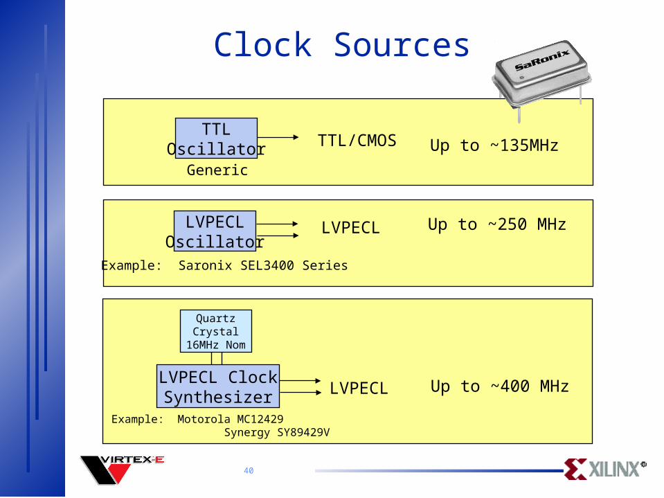
Clock Sources
TTLOscillator
LVPECLOscillator
QuartzCrystal
16MHz Nom
LVPECL ClockSynthesizer
Example: Motorola MC12429 Synergy SY89429V
Up to ~135MHz
Up to ~250 MHz
Up to ~400 MHz
Example: Saronix SEL3400 Series
Generic
LVPECL
TTL/CMOS
LVPECL

41
Virtex-E 300+ MHz LVPECL Clocking
Virtex-E Eliminates PECL-to-TTL Converters -- Eliminates 2ns Delay & SkewTypical Discrete Solution: Motorola MC100EPT23 Dual Differential PECL to TTL Translator, TPD = 2.0ns
LVPECL Clock Source
LVPECL Clock Source
LVPECL Clock
Distributor
LVPECL Clock
Distributor
2 2
2
Virtex-E 1Virtex-E 1
Virtex-E nVirtex-E n
Virtex-E 2Virtex-E 22
Example Devices:Motorola MC10/100E111
Synergy SY10E111LEVirtex-E
No LVPECL-TTL Translator
Equal-Length Point-to-Point LVPECL PCB Clock Traces

42
Virtex-E LVPECL Clock Conversion Receive and convert high speed clocks with zero delay
ExternalRAM, etc.
ExternalRAM, etc.
ExternalRAM, etc.
ExternalRAM, etc.
Zero-Delay Local Clock Generation to Any of Virtex-E I/O Standards
SSTL
TTL
DLL
DLL
Virtex-E
LVPECL Clock
43
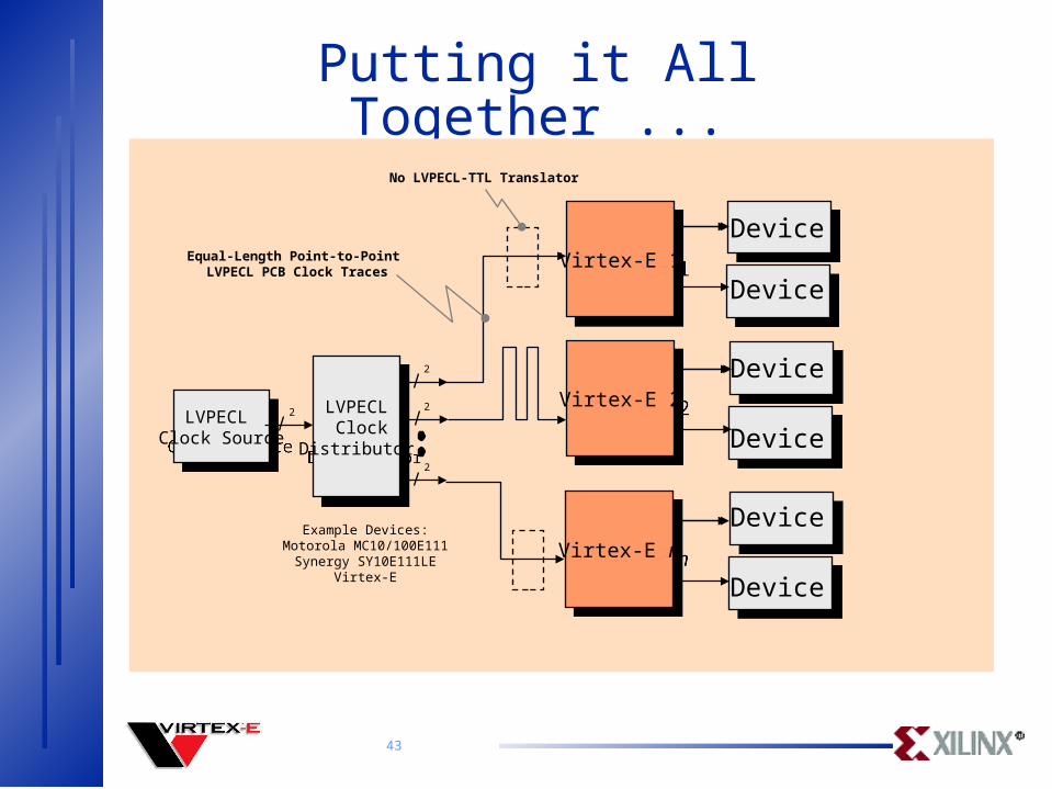
Putting it All Together ...
LVPECL Clock Source
LVPECL Clock Source
LVPECL Clock
Distributor
LVPECL Clock
Distributor
2 2
2
Virtex-E 1Virtex-E 1
Virtex-E nVirtex-E n
Virtex-E 2Virtex-E 2
2
Example Devices:Motorola MC10/100E111
Synergy SY10E111LEVirtex-E
No LVPECL-TTL Translator
Equal-Length Point-to-Point LVPECL PCB Clock Traces
Device
Device
Device
Device
Device
Device

44
Designing With LVDS and LVPECL
Some Facts— Impedance Matching is VERY important — Discontinuities in impedance WILL create
reflections.— Reflections degrade signals and show up as
Common Mode Noise.— Common Mode Noise cancels the magnetic shield
effect of differential lines and radiates as EMI.— Do not make sharp turns since this causes
impedance discontinuities.— Keep stubs and uncontrolled tracks < 10 mm.

45
Designing With LVDS and LVPECL (Continued)
PCB guidelines:— Use at least 4 PCB layers (LVDS signals, ground, power, TTL/CMOS
signals)
— Separate TTL/CMOS signals from the LVDS signals— Keep LVDS driver/receiver connections as close to the
connectors as possible.— Decouple the power supply as good as possible.— Connect all the VCC and Ground pins of the
component.— Make power and ground tracks as wide as possible.— Connect to power and ground tracks with multiple vias.
46
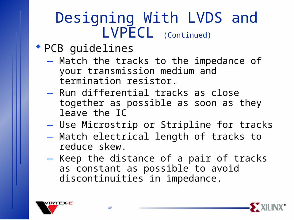
Designing With LVDS and LVPECL (Continued)
PCB guidelines— Match the tracks to the impedance of your
transmission medium and termination resistor.— Run differential tracks as close together as
possible as soon as they leave the IC — Use Microstrip or Stripline for tracks — Match electrical length of tracks to reduce skew.— Keep the distance of a pair of tracks as constant
as possible to avoid discontinuities in impedance.

47
Designing With LVDS and LVPECL (Continued)
R
R/2
R/2C
PCB guidelines— Use a good matching termination resistor.
– LVDS will not work without resistor termination.
— Typically a single resistor at the receiver is OK.— Surface mount resistors are best.
– Stubs are short.– Distance between receiver and termination is short.– No component leads.
— At extra cost you can use the center tap capacitance termination scheme.

48
More LVDS and LVPECL Info
Look at AppNotes XAPP230, XAPP231, XAPP232
At Xilinx’ website:http://www.xilinx.com/apps/xapp.htm

49
Memory Interfaces
ZBT RAM, SDRAM, DDR SDRAM

50
Virtex-E and High Speed Memory Interfaces
Features needed for interface to high speed memory— Fast I/Os— Clock management capabilities
Virtex-E has both:— SSTL2, HSTL, LVDS, LVPECL and many more— 8 on-chip DLLs - use for Clk-to-Out speed up,
clock deskew, clock multiplication/division

51
Benefits of using an FPGA for the Memory Interface
Easy to implement
Can add functionality in the future easily— ASIC is a one-time-deal
Combine multiple discrete devices into the FPGA— Save space, money, and power

52
High Speed Memory Interfaces
ZBT RAM Interface
SDRAM Interface
DDR SDRAM Interface

53
Zero Bus Turn-around SRAM
Extremely high bandwidth — Other non-cache applications in telecom, test equipment, DSP
and embedded memory applications
ZBT stands for “Zero Bus Turnaround” — No idle cycles between read-to-write and write-to-read — 100% bus use — Previous architectures had a Turnaround Cycle
Completely Deterministic Timing - Simplifies System Design— Any cycle can perform any operation

54
ZBT SRAM Parameters
Densities 2, 4 and 8 Mbits
Data bus widths 18, 32, and 36-bit
IO Voltage and standards 2.5V, 3.3V, LVTTL
Flow thru speed 8, 10ns (Clock cycle time)
Pipeline speed 5, 6, 7.5ns (Clock cycle time)

55
ZBT Flow-ThroughTiming
Write Operation - “Late Write” data to be written is presented on next clock
Read Operation - data available after single clock latency
Control
Data
Address
Clk 1 2
Control
Data
Address
Clk 1 2

56
ZBT Pipelined Timing
Read Operation - data available after two clock latency
Write Operation - “Late Write” data is written 2 cycles later
Control
Address
Clk 1 2 3
Data
Control
Address
Clk 1 2 3
Data

57
ZBT 100% Bus UseWrite/Write/Read/Write/Read/Burst Read
Write1 WRITE3Write2 Read1 Read2 RdBrst
Addw1 Addw3Addw2 AddR1 AddR2
Doutw3
DinR1
T4T1 T3T2 T5 T6 T8T7
Clock
Command
Address
DQDoutw1
Doutw2
DinR2
DinR2+1
Pipelined part’s timing is illustrated above

58
Virtex-E ZBT Bandwidth 800 Mbytes/sec @ 32bits wide
DeviceFrequency
(MHz)CycleTime(nS)
MAX*Bandwidth(MByte/sec)
READ/WRITECycle
Bandwidth
READ/WRITEBurst of 4Bandwidth
ZBT Pipelined 200 5 800 800 800ZBT Pipelined 166 6 666 666 666ZBT Pipelined 143 7 572 572 572ZBT Pipelined 133 7.5 533 533 533
SyncBurst Pipelined 133 7.5 533 267 426ZBT FlowThrough 100 10 400 400 400
SyncBurst Flow-Through 83 12 332 221 295
NOTE:The bandwidth figures presented in this table are for a 32 bit data path, theraw bandwidth is 12.5% higher if a 36 bit data path is used.
Very High Performance Synchronous, Static Memory

59
ZBT Interface Reference Design
CLKin
Data
Error
Reset
DLL 2
DLL 1
Tester
Data out
Data in
Addr
RW#
Clk2x
XCV300-E
Clk2x
ZBT SRAM
AddrController

60
ZBT Interface Application Note
•7.2 Giga-bits/s @ 36 bits wide
•200 MHz Synthesisable HDL Controller Design
•XCV300-E, -6 speed grade
ZBT Controller Interface with tester resource utilisation93 Logic Cells502 Flip Flops
71 IO
PartLogicCell
Utilisation
Totalavailable
LogicCells
Flip FlopUtilisation
TotalavailableFlip Flops
IOUtilisation
Totalavailable
IO
XCV50-E 5.38% 1,728 32.68% 1536 39.44% 180XCV100-E 3.44% 2,700 20.92% 2400 39.44% 180XCV200-E 1.76% 5,292 10.67% 4704 25.00% 284XCV300-E 1.35% 6,912 8.17% 6144 22.47% 316XCV400-E 0.86% 10,800 5.23% 9600 17.57% 404XCV600-E 0.60% 15,552 3.63% 13824 13.87% 512XCV1000-E 0.34% 27,648 2.04% 24576 13.87% 512

61
ZBT Bus Contention - Real World
143 MHz Clock
R/W
Address [0]
Data [0]
Scope shot taken directly from the ZBT controller reference board.

62
Virtex-E High Speed SDRAM Interface
SDRAM Overview— Features
Virtex-E SDRAM controller— Features— Block diagram— Timing
63
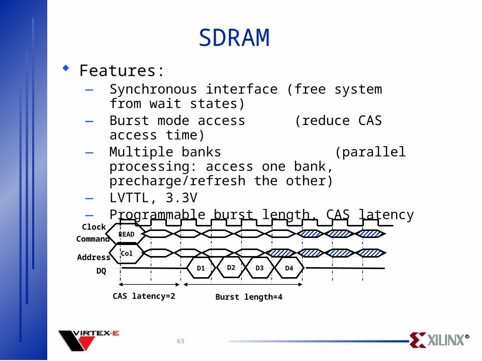
SDRAM Features:
— Synchronous interface (free system from wait states)— Burst mode access (reduce CAS access time)— Multiple banks (parallel processing: access one bank,
precharge/refresh the other)— LVTTL, 3.3V— Programmable burst length, CAS latency
CAS latency=2 Burst length=4
READ
Col
D4D3
Clock
Command
Address
DQ D1 D2

64
SDRAM Controller Application Note
Synthesizable Verilog/VHDL
Programmable burst length (1, 2, 4, 8)
Programmable CAS latency (2, 3)
Automatically issues refresh commands
Supports LOAD_MR, AUTO_REFRESH, PRECHARGE, ACT_ROW, READA, WRITEA, BURST_STOP, NOP
Interfaces with SDRAM at 125MHz (Virtex-E, -6 speed)
Uses 2 DLLs and 165 CLB slices (5% of XCV300E)

65
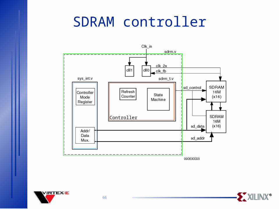
SDRAM controller
XCV300-E-6
SDRAM16M(x16)
125MHz clock
controls
addr
data
11
32
controls
data_addr_n
AD
32
system
62.5MHz clock
66
SDRAM controller
Controller

67
SDRAM controller IO timing
Read Cycle is the critical timing:— SDRAM-8 clk-to-out = 6.0ns— Virtex-6 setup = 1.7ns— 125 MHz operation (8ns cycle), 300ps left for board routing on
data lines
Write Cycle:— Virtex-6 clk-to-out = 3.9ns— SDRAM-8 setup = 2.0ns— 125 MHz operation (8ns cycle), 2.1ns left for board routings

68
Virtex-E DDR-SDRAM Interface
DDR SDRAM Overview— Features— Differences from SDRAM
Virtex-E SDRAM controller— Features— Block diagram— Timing— Board layout guideline

69
DDR SDRAM Features:
— Next generation SDRAM— DDR data I/O (twice the bandwidth at the same
clock frequency as SDRAM)— Peak bandwidth: 1.6 GBytes/s (64-bit @ 100MHz)— 2.5V, SSTL2, 100/133MHz— Advantages over RDRAM cost, package, open
industry spec, compatible with existing spec— Supported by major vendors Micron, Samsung, IBM,
Fujitsu, Hitachi, Huyndai, Toshiba,...

70
DDR SDRAM
Differences compared to standard SDRAM:— All IOs are SSTL2, 2.5V (reduce power and noise)— Differential clock (CLK and CLKB). Positive edge
clock is the crossing of CLK going high and CLB going low.
— Bidirectional data strobe (clock-to-data skew is eliminated)
— Double Data Rate data transfer

71
Write Cycle
ACT NOP WRITE
ROW COL
D1 D2 D4D3
ACT NOP WRITE
ROW COL
D1 D3D2 D4
DDR SDRAM:
SDRAM:
clk
cmd
addrdata
cmd
addrdqs
data
clkbclk

72
Read Cycle
DDR SDRAM:
SDRAM:
ACT NOP READ
ROW COL
D1 D2 D4D3
clk
cmd
addrdata
ACT NOP READ
ROW COL
cmd
addrdqs
data
clkbclk
D1 D3D2 D4

73
DDR SDRAM controller Application Note
Synthesizable Verilog
Virtex-E, -6 speed grade: 100 MHz Clk — 200 MHz Data rate— 1.6 Giga-Bytes/S bandwidth @ 64 bits wide
Programmable CAS latency, burst length
2 DLLs, 474 slices (15% of XCV300-E)
Uses “Logic Accessible Clock” technique
Uses Clock to latch Read Data, instead of DQS

74
DDR SDRAM controller
Virtex-E

75
DDR SDRAM IO timingData Lines: Read Cycle
Data Lines— Read cycle is critical. Data is strobed by clk,
instead of DQS
ddr_clk
-0.8nsminimum DDR clk-out
-0.4ns minimum Virtex-E hold time
Minimum trace delay on data = 0.8ns - 0.4ns - clock skew between ddr_clk & fpga_clk = 0.4ns- clock skew

76
DDR SDRAM IO timingAddr/Cntrl Lines
Address and Control lines are generated on the negative edge of the clock, to guarantee DDR hold time
Maximum trace delay on Addr/Cntrl = 5ns - 2.4ns - 1.2ns - clock skew
= 1.4ns - clock skew
ddr_clk
2.4ns
1.2ns
Virtex-E clk_out (max)
DDR setup time
5ns

77
DDR SDRAM IO timingSummary
The I/O spec for DDR is very tight
Carefully calculate data and address trace delays to guarantee setup and hold times
The minimum trace delay on the data lines can be eliminated by delaying the ddr_clk— Since DDR has negative tAC(min), delaying the ddr_clk
helps meet Virtex-E’s hold time requirement

78
Board Layout Guideline All high speed memory interfaces
— Virtex device and the memory chips must be placed close to each other
— Consider/Simulate board level signal integrity and timing, pay particular attention to clocks
— Use matched impedance traces
DDR — All bi-directional signals use IOBUF_SSTL2_II (data & data strobes)
other output signals use OBUF_SSTL2_I— DQ lines must be closely matched, and kept short to minimize cross
talk— DQS trace lengths should match DQ— CLK and CLKB delays and loads should match (CLKB can also be
routed back to an unused IOB near the feedback pin)
79
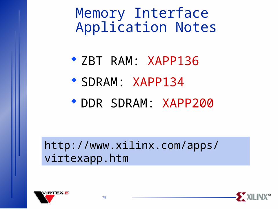
Memory Interface Application Notes
ZBT RAM: XAPP136
SDRAM: XAPP134
DDR SDRAM: XAPP200
http://www.xilinx.com/apps/virtexapp.htm

80
CAM in Virtex-E

81
CAM Overview
Content Addressable Memory
Storage Array (like RAM)
Find a location of a particular stored value
Compare input against data in memory– If Match found, output the Address– Maximum performance, if match in a single
clock cycle

82
CAM Overview
Simple RAM and CAM compared
Add [9:0] 1024 x 8
RAM
Dout [7:0]
1024 x 8
CAM
Din [7:0]
Add [9:0]
Match
83
CAM Applications
Telecommunications
Networking
Ethernet
ATM
Protocol

84
CAM Overview
CAM features:— Word Size (width)— Number of Words (depth)— Match or Compare Time (read)— Significance of Write Speed— Clock Frequency— Masks— Decoded and/or Encoded Address (outputs)

85
CAMs in Virtex-E
Flexible CAM designs in Virtex and Virtex-E— CAM implemented in a LUT— CAM implemented in a Block SelectRAM
Depth Width Size Match Device Logic32 8 256 bits 4.5 ns XCV50-6 BRAM
256 8 2Kbits 8.5 ns XCV50E-6 BRAM32 16 512 bits 8 ns XCV50-6 SRL16
128 40 5Kbits 12 ns XCV300-6 SRL164096 16 64Kbits 16 x 20 ns XCV400-6 RAM16x1

86
Designing CAM in Virtex slices
XAPP203: “Designing Flexible, Fast CAMs with Virtex Family FPGAs”:— VHDL and Verilog Reference Designs available
Features— 4 bits per LUT— 16-word x 4-bit organization— Match in one clock cycle— 16 Write clock cycles— Decoded address output— Generic word width from 4 bits up to any multiple by 4— Generic number of 16 words CAM blocks— Cascadable— Address Encoder in logic or tri-state buffers (TBUF)

87
CAM in a LUTMatch Operation
DATA_IN
Reconfigurable 8-bit Word Comparator
8
LUT
LUT
SRL16
D Q
A[0:3]
SRL16
D Q
A[0:3]
“1”
Wide AND
FF
D Q
CLK
MATCH_SIGNAL
1 slice
4
4

88
Match Waveforms for CAM in a LUT
CAM16WORDS
ENCODEMATCHDATA_IN
MATCH_ENABLE
R_MATCH_ADDR
R_MATCH_OK
DATA_IN “…1001”
MATCH “xxxx xxxx xxxx xxxx” “0000 0000 0000 0100”
MATCH_ENABLE
R_MATCH_OK
R_MATCH_ADDR “xxxx” “0010”
CLK
Match_cycle Encode_cycle

89
CAM in a LUTWrite Operation
Counter
4-bit Compare
4-bit Compare
Reconfigurable 8-bit Word Comparator
4
8DATA_IN
LUT
LUT
SRL16
D Q
A[0:3]
SRL16
D Q
A[0:3]
1 slice
MSB
4
LSB
4

90
Cascading CAMs in LUTs CAM match path (1 CLK) & encode (1 CLK)
MATCH_ENABLE
DATA_IN
CLK
CAM_16WORDS Encode4 LSB
Encode4 LSB
Encode4 LSB
EncodeMSB
FF
D Q
FF
D Q
16 FFs
MATCH_ADDR
MATCH_OK
CAM_16WORDS
CAM_16WORDS
CAM_16WORDS Encode4 LSB
16
Array of N x 16_WORDS8

91
CAM in Block SelectRAM
XAPP204: “Using Block SelectRAM+ for High-Performance Read/Write CAMs”:— VHDL and Verilog Reference Designs available
Features— 128 bits per Block SelectRAM+— 16-word x 8-bit organization— Match in one clock cycle— Write in one clock cycle (and Erase in one clock cycle)— Decoded address output— Fully synchronous match and write ports (Independent)— Cascadable— Address Encoder in logic or tri-state buffers (TBUF)

92
CAM in a Block SelectRAM+
CAM 16x8 Macro in 1 Block SelectRAM+
MATCH[15:0]
DATA_WRITE[7:0]
ADDR[3:0]
ERASE_WRITE
CLK_WRITE
DATA_MATCH[7:0]
WRITE_ENABLE
MATCH_ENABLE
MATCH_RST
CLK_MATCH
RAMB4_S1_S16
DOB[15:0]
DOA N.C.
DIA[0]
ADDRA[11:0]
WEA
ENA
RSTA
CLKA
DIB[15:0]
ADDRB[7:0]
WEB
ENB
RSTB
CLKB
“0000….0000”
“0”
“0”
128
4
PORT A
PORT B

93
Cascading Block SelectRAM+ CAMs for bigger depth
CAM 64-word x 8-bit in Read Mode
CAM (16x8)
CAM (16x8)
CAM (16x8)
CAM (16x8)
16
32
48
64
MATCH[63:0]
DATA_MATCH[7:0]
CLK_MATCH
8
[15:0]
[31:16]
[47:32]
[63:48]
8
8
8

94
Cascading Block SelectRAM+ CAMs for higher width
CAM 16-word x 16-bit in Read Mode
CAM (16x8)
DATA_MATCH[15:0]
CLK_MATCH[15:0]
[15:0]
[15:8]
[7:0]
MATCH[15:0]
[0]
[0][0]
[1]
[1][1]
[15]
[15][15]
CAM (16x8)

95
CAM in Block SelectRAM+The final picture
CAM16x8 Macro— Match flag and encoded outputs
DATA[7:0]
Write port A(4096 x 1)
Read port B(256 x 16)
MATCH[15:0]
CLKBCLK_MATCH
ADDRB[7:0]
DOB[15:0]
Decoded Address
16
FF
D Q
ENCODEMATCH_ADDR[3:0]
4
MATCH_SIGNAL
CLK_MATCH
96
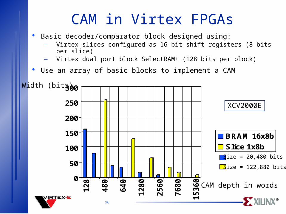
CAM in Virtex FPGAs Basic decoder/comparator block designed using:
— Virtex slices configured as 16-bit shift registers (8 bits per slice)— Virtex dual port block SelectRAM+ (128 bits per block)
Use an array of basic blocks to implement a CAM
0
50
100
150
200
250
300128
480
640
1280
2560
7680
15360
BRAM 16x8b
Slice 1x8b
CAM depth in words
Width (bits)
XCV2000E
Size = 20,480 bits
Size = 122,880 bits

97
XILINX CAMs comparison
Device VIRTEX & VIRTEX-E VIRTEX & VIRTEX-E VIRTEX & VIRTEX-EImplementation Slices RAM16x1 based Slices SRL16 based Block SelectRAMMin. CAM size 10 bits per LUT 4 bits per LUT 128 bits per BlockMax CAM size ~ 500 Kbits (XCv3200E) ~200 Kbits (XCV3200E) 26 Kbits (XCV3200E)MATCH (# of clock) 16 cycles 1 cycle 1 cycleWRITE (# of clock) 1 cycle 16 cycles 1 cycle (+1 erase cycle)Min. CAM width 1 bit 4 bits 8 bitsMin. CAM depth 16 words 1 word 16 wordsMax. CAM depth ~64 K 8-bit words ~25 K 8-bit words 3,328 8-bit wordsFastest Match 16 x 12 ns 7.5 ns 4.5 nsDecoded Address yes (by 16) yes yesDesign Ref. Design 202 Ref. Design 203 Ref. Design 204

98
SRL16

99
SelectShift
D QCE
D QCE
D QCE
D QCE
LUT
INCE
CLK
ADDR[3:0]
OUT
Slice
LUT
LUT
Slice
LUT
LUT
CLB
0
1
2
15
Dynamically addressable Shift Registers, implemented in one LUT

100
SelectShift Features
Serial In, Serial Out
Does not require an address counter
Programmable cycle delay from 1 to 16— Addr[3:0] specifies the desired delay
Cascade for cycle delays greater than 16
CLB Flip-Flops can be used to add depth

101
Software Support
Primitives available in software
Positive or negative clock edge triggered
Clock Enable optional
Available for VHDL or Verilog instantiations
DCLK
A3A2A1A0
QSRL16
16-bit Shift Register Look-Up-Table
D
CLK
A3A2A1A0
QSRL16ECE
16-bit Shift Register Look-Up-Table with Clock Enable
102
SRL16 Applications
Shift Registers
Delayed Signal Generation
Linear Feedback Shift Registers (LFSRs)
CRC circuits

103
Virtex- E Configuration

104
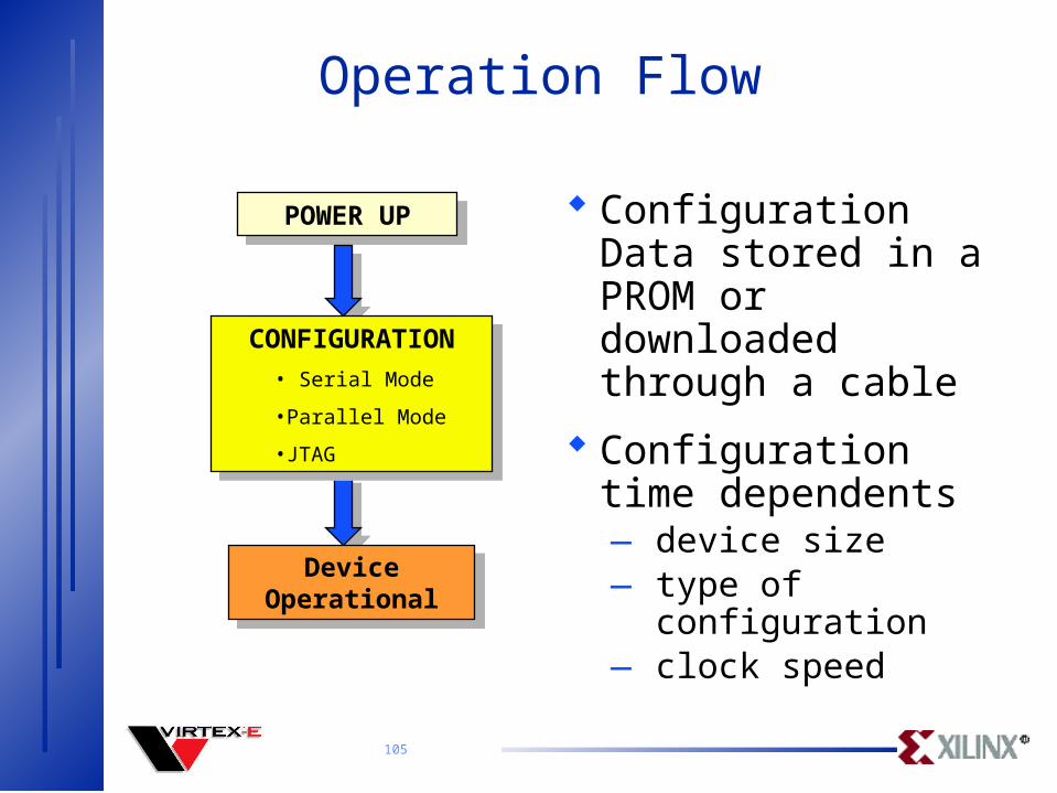
Agenda Review of configuration Modes
— Serial, Parallel, JTAG
Startup Sequence
XC1800 PROM interfacing
Daisy Chaining
Tips in debugging configuration issues
JTAG Configuration
105
POWER UPPOWER UP
Device Operational
Device Operational
CONFIGURATION
• Serial Mode
•Parallel Mode
•JTAG
CONFIGURATION
• Serial Mode
•Parallel Mode
•JTAG
Operation Flow
Configuration Data stored in a PROM or downloaded through a cable
Configuration time dependents — device size — type of configuration — clock speed
106
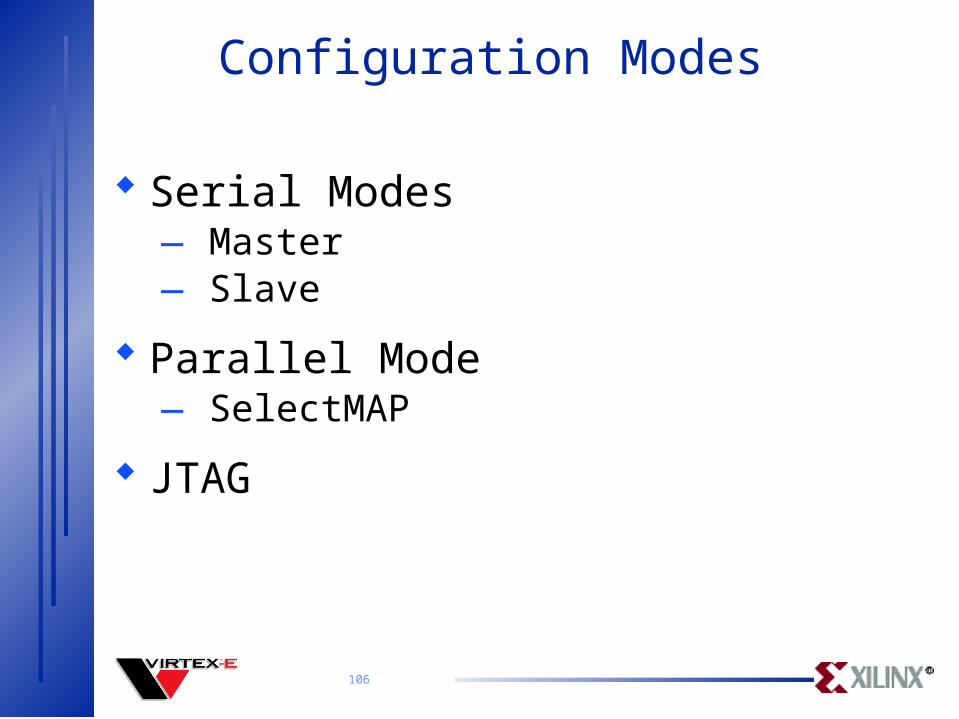
Configuration Modes
Serial Modes— Master— Slave
Parallel Mode— SelectMAP
JTAG

107
Serial Mode Configuration
PROM
CLK
DATA
/CE
/RESET/OE
Virtex-E
CCLK
DIN
DONE
/INIT
Serial Configuration— Master mode: the Virtex-E device is initiating the
configuration— Slave mode: the Virtex-E device is waiting for
some other device to start the configuration
Master Serial Configuration Mode

108
Serial Mode Configuration
Data is loaded serially- one bit per CCLK
A Virtex-E device in Master Serial Mode produces it’s own CCLK— CCLK rate is controllable in software— Mode used with a PROM
In a Slave Serial Mode, Virtex-E device needs a CCLK provided by another device— All download cables do this
109
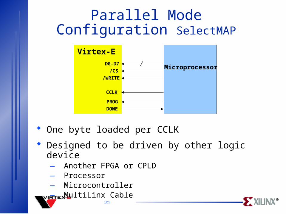
Parallel Mode Configuration SelectMAP
One byte loaded per CCLK
Designed to be driven by other logic device— Another FPGA or CPLD— Processor— Microcontroller— MultiLinx Cable
Microprocessor
Virtex-E
CCLK
D0-D7
DONE
/CS
/WRITE
PROG

110
Important Signals in SelectMAP
Data(D0-D7)- bi-directional data bus— D0 is the MSB
/WRITE- direction of data on the bus — Low for configuration (Write)— High for readback
/CS- enable for the data bus— a High will ignore CCLK transitions
BUSY- output that indicates when data can be received— Not needed for CCLK < 50 MHz
111
SelectMAP- Things to Know
Initialization needed after /INIT goes high— 3 CCLKs needed— If /CS and /WRITE are asserted early , no data
will be transferred on the first CCLK
To strobe data, use /CS, not /WRITE— If a CCLK rising edge occurs when /CS is
asserted and /WRITE is de-asserted, an ABORT will occur– Need to reload Sync Word and redo last
packet

112
Virtex-E Bitstream Format
10 internal configuration registers
Bitstream is actually a set sequence of writes into those registers
Configuration data still broken into frames
All data is encapsulated into packets- Type I and Type II
When migrating from Virtex to Virtex-E a new bitstream is needed

113
Configuration Registers
RegisterSymbol
Register Name/Description
CMD Command Register- executes commands to control read/write, CRC, etc.
FLR Frame Length- indicates frame size (available in XAPP138)
COR Configuration Option Register- some user selected options from Bitgen
MASK Mask Register- masks out bits of CTL register for security
CTL Control Register- handles internal functions like Port Persistence
FAR Frame Address Register- sets the starting frame address
FDRI Frame Data Input- pipelined input register that receives frame data
CRC Cyclic Redundancy Check- loaded with CRC value that checks for errors
FDRO Frame Data Output- pipelined output register for reading frame data
LOUT Legacy Data Output- pipelines data to the DOUT pin
Each register has a 5-bit address
Detailed information in XAPP 138

114
Configuration Startup Sequence
Four signals to control— GWE (Global Write Enable)— GSR (Global Set/Reset)— GTS (Global 3-State)— DONE (External Done Pin)
Six phases to select assertion/de-assertion (1-6)
Sequencer will wait in the DONE phase until DONE goes high
Can create “Sync-To-Done” behavior by setting GTS, GSR, and GWE to same cycle as DONE

115
Startup Sequence
StartupClk
Phase 0 1 2 3 4 5 6 7
DONE
GTS
GSR
GWE
DefaultPhase in
Bold

116
Virtex-E and XC1800 PROM’s
Can program via serial or SelectMAP mode— serial vs. parallel controlled in software
117
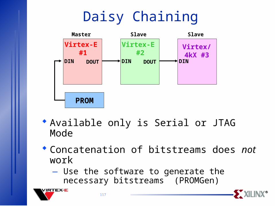
Daisy Chaining
Available only is Serial or JTAG Mode
Concatenation of bitstreams does not work— Use the software to generate the necessary
bitstreams (PROMGen)
Virtex-E #1
Virtex-E #2
Virtex/4kX #3
PROM
DIN DIN DINDOUT DOUT
Master Slave Slave

118
Debugging Tips and Info
What causes /INIT to go low? — CRC check fails— Internal error, e.g. data loaded too fast
When will an error stay undetected?— A bit is missed or added- this will misalign the
instructions, and the CRC check won’t happen
Mode pin considerations— Internal pullups are guaranteed— Make sure pulldown is strong enough (4.7k)

119
JTAG Configuration

120
JTAG - Joint Test Action Group— Developed as standard testing interface— Boundary Scan, IEEE STD 1149.1
Four Dedicated Pins Required:— TDI, TDO, TMS, and TCK — TRST is an optional 5th pin that Xilinx does not
use
What is JTAG?

121
JTAG Standard
JTAG Standard - 16 State, State Machine— TAP (Test Access Port)— IR (Instruction Register) — DR (Data Register)— Bypass Register

122
JTAG Tap Controller
0
Test-Logic-Reset
Exit2-DR
Capture-DR
Shift-DR
Exit1-DR
Select-IR-Scan
Capture-IR
Shift-IR
Exit1-IR
Pause-DR
Pause-DR
Run-Test/Idle Select-DR-Scan
Update-IR
Exit2-DR
Update-DR
1 1 1
1
1
11
1
1
1
1
1
1
0
0
0
0
0
0
0
0
0
0
1
0
0
1
0

123
JTAG TAP Controller:Architecture

124
BSDL Files
Boundary Scan Description Language
BSDL Files define the hardware— Description of the die, with pins and scan chain
order— Information about the size of the various chip
specific registers (e.g. instruction register length)
Unconfigured BSDL files are provided— Assumes all I/Os are bidirectional

125
Files on the web are continuously updated— Current software does not always have most
recent BSDL file
HTTP://support.xilinx.com -> Software
BSDL Availability

126
JTAG Programmer Software Support for Virtex-E
JTAG Software Support in M2.1i SP3 — Non invasive: Idcode, Bypass, Usercode— SVF file generation
Stay current with the download tools — Service packs— Web Pack (pc only)
Foundation or Alliance software updates at: http://support.xilinx.com/support/techsup/sw_updates/
Foundation or Alliance software updates at: http://support.xilinx.com/support/techsup/sw_updates/
JTAG Programmer at:http://www.xilinx.com/sxpresso/webpack.htm
JTAG Programmer at:http://www.xilinx.com/sxpresso/webpack.htm

127
Cables
Provided by Xilinx
Multilinx— Supported in 2.1i sp2 JTAG Programmer— USB or Serial ports— Win 98 only
Parallel Cable III
XChecker

128
Cables: JTAG Connections
* If there is a TRST trace on the board, it should be tied high

129
JTAG Debugging Tips
Debug Chain Software Tool (Logic Probe)
/TRST pin should be tied high on 3rd party chips
Noise or bad parallel port
ISP Checklist app note XAPP104
Know all devices in chain and the order
Virtex-E does not tolerate 5V signals directly

130
Good References Virtex-E Datasheet- basic information on configuration modes
XAPP138- Configuration modes, packets and readback
XAPP151- Detailed bitwise explanation of configuration registers, partial reconfiguration hints and advanced concepts in readback
XAPP139 - Detailed information on JTAG configuration and readback for VIRTEX devices
XAPP153 - Status and Control register information for partial reconfiguration information
http://www.xilinx.com/apps/virtexapp.htm