Embed Size (px)
Citation preview
To our customers,
Old Company Name in Catalogs and Other Documents
On April 1st, 2010, NEC Electronics Corporation merged with Renesas Technology
Corporation, and Renesas Electronics Corporation took over all the business of both companies. Therefore, although the old company name remains in this document, it is a valid Renesas Electronics document. We appreciate your understanding.
Renesas Electronics website: http://www.renesas.com
April 1st, 2010 Renesas Electronics Corporation
Issued by: Renesas Electronics Corporation (http://www.renesas.com)
Send any inquiries to http://www.renesas.com/inquiry.
Notice 1. All information included in this document is current as of the date this document is issued. Such information, however, is
subject to change without any prior notice. Before purchasing or using any Renesas Electronics products listed herein, please confirm the latest product information with a Renesas Electronics sales office. Also, please pay regular and careful attention to additional and different information to be disclosed by Renesas Electronics such as that disclosed through our website.
2. Renesas Electronics does not assume any liability for infringement of patents, copyrights, or other intellectual property rights of third parties by or arising from the use of Renesas Electronics products or technical information described in this document. No license, express, implied or otherwise, is granted hereby under any patents, copyrights or other intellectual property rights of Renesas Electronics or others.
3. You should not alter, modify, copy, or otherwise misappropriate any Renesas Electronics product, whether in whole or in part. 4. Descriptions of circuits, software and other related information in this document are provided only to illustrate the operation of
semiconductor products and application examples. You are fully responsible for the incorporation of these circuits, software, and information in the design of your equipment. Renesas Electronics assumes no responsibility for any losses incurred by you or third parties arising from the use of these circuits, software, or information.
5. When exporting the products or technology described in this document, you should comply with the applicable export control laws and regulations and follow the procedures required by such laws and regulations. You should not use Renesas Electronics products or the technology described in this document for any purpose relating to military applications or use by the military, including but not limited to the development of weapons of mass destruction. Renesas Electronics products and technology may not be used for or incorporated into any products or systems whose manufacture, use, or sale is prohibited under any applicable domestic or foreign laws or regulations.
6. Renesas Electronics has used reasonable care in preparing the information included in this document, but Renesas Electronics does not warrant that such information is error free. Renesas Electronics assumes no liability whatsoever for any damages incurred by you resulting from errors in or omissions from the information included herein.
7. Renesas Electronics products are classified according to the following three quality grades: “Standard”, “High Quality”, and “Specific”. The recommended applications for each Renesas Electronics product depends on the product’s quality grade, as indicated below. You must check the quality grade of each Renesas Electronics product before using it in a particular application. You may not use any Renesas Electronics product for any application categorized as “Specific” without the prior written consent of Renesas Electronics. Further, you may not use any Renesas Electronics product for any application for which it is not intended without the prior written consent of Renesas Electronics. Renesas Electronics shall not be in any way liable for any damages or losses incurred by you or third parties arising from the use of any Renesas Electronics product for an application categorized as “Specific” or for which the product is not intended where you have failed to obtain the prior written consent of Renesas Electronics. The quality grade of each Renesas Electronics product is “Standard” unless otherwise expressly specified in a Renesas Electronics data sheets or data books, etc.
“Standard”: Computers; office equipment; communications equipment; test and measurement equipment; audio and visual equipment; home electronic appliances; machine tools; personal electronic equipment; and industrial robots.
“High Quality”: Transportation equipment (automobiles, trains, ships, etc.); traffic control systems; anti-disaster systems; anti-crime systems; safety equipment; and medical equipment not specifically designed for life support.
“Specific”: Aircraft; aerospace equipment; submersible repeaters; nuclear reactor control systems; medical equipment or systems for life support (e.g. artificial life support devices or systems), surgical implantations, or healthcare intervention (e.g. excision, etc.), and any other applications or purposes that pose a direct threat to human life.
8. You should use the Renesas Electronics products described in this document within the range specified by Renesas Electronics, especially with respect to the maximum rating, operating supply voltage range, movement power voltage range, heat radiation characteristics, installation and other product characteristics. Renesas Electronics shall have no liability for malfunctions or damages arising out of the use of Renesas Electronics products beyond such specified ranges.
9. Although Renesas Electronics endeavors to improve the quality and reliability of its products, semiconductor products have specific characteristics such as the occurrence of failure at a certain rate and malfunctions under certain use conditions. Further, Renesas Electronics products are not subject to radiation resistance design. Please be sure to implement safety measures to guard them against the possibility of physical injury, and injury or damage caused by fire in the event of the failure of a Renesas Electronics product, such as safety design for hardware and software including but not limited to redundancy, fire control and malfunction prevention, appropriate treatment for aging degradation or any other appropriate measures. Because the evaluation of microcomputer software alone is very difficult, please evaluate the safety of the final products or system manufactured by you.
10. Please contact a Renesas Electronics sales office for details as to environmental matters such as the environmental compatibility of each Renesas Electronics product. Please use Renesas Electronics products in compliance with all applicable laws and regulations that regulate the inclusion or use of controlled substances, including without limitation, the EU RoHS Directive. Renesas Electronics assumes no liability for damages or losses occurring as a result of your noncompliance with applicable laws and regulations.
11. This document may not be reproduced or duplicated, in any form, in whole or in part, without prior written consent of Renesas Electronics.
12. Please contact a Renesas Electronics sales office if you have any questions regarding the information contained in this document or Renesas Electronics products, or if you have any other inquiries.
(Note 1) “Renesas Electronics” as used in this document means Renesas Electronics Corporation and also includes its majority-owned subsidiaries.
(Note 2) “Renesas Electronics product(s)” means any product developed or manufactured by or for Renesas Electronics.
APPLICATION NOTE
REJ05B0800-0100/Rev.1.00 March 2006 Page 1 of 36
H8SX Family Using the Average Transfer Rate Generator in Transmission and Reception via the SCI (Serial Communications Interface): DMAC Volume
Introduction In the H8SX/1653, an average transfer rate generator can be selected as the clock source for serial communications interfaces 5 and 6 (SCI_5 and 6) in the asynchronous mode. In this sample task, the average transfer rate generator is used to drive the transfer of data at a rate of 921.569 kbps in operation at Pφ = 16 MHz.
Target Device H8SX/1653
Contents
1. Specifications.................................................................................................................................... 2
2. Applicable Conditions ....................................................................................................................... 3
3. Description of Modules Used............................................................................................................ 4
4. Description of Operation ................................................................................................................. 10
5. Description of Software................................................................................................................... 14
H8SX Family
Using the Average Transfer Rate Generator in Transmission and Reception via the SCI (Serial Communications Interface): DMAC Volume
REJ05B0800-0100/Rev.1.00 March 2006 Page 2 of 36
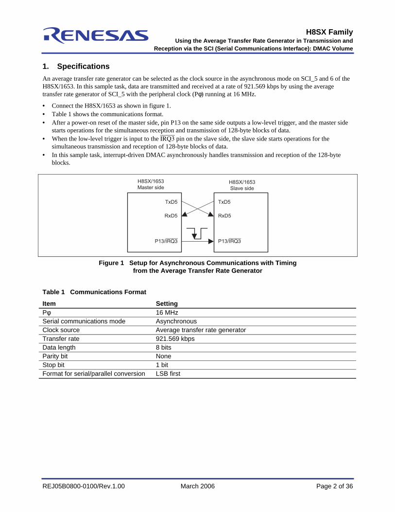
1. Specifications An average transfer rate generator can be selected as the clock source in the asynchronous mode on SCI_5 and 6 of the H8SX/1653. In this sample task, data are transmitted and received at a rate of 921.569 kbps by using the average transfer rate generator of SCI_5 with the peripheral clock (Pφ) running at 16 MHz.
• Connect the H8SX/1653 as shown in figure 1. • Table 1 shows the communications format. • After a power-on reset of the master side, pin P13 on the same side outputs a low-level trigger, and the master side
starts operations for the simultaneous reception and transmission of 128-byte blocks of data. • When the low-level trigger is input to the IRQ3 pin on the slave side, the slave side starts operations for the
simultaneous transmission and reception of 128-byte blocks of data. • In this sample task, interrupt-driven DMAC asynchronously handles transmission and reception of the 128-byte
blocks.
H8SX/1653
Master sideH8SX/1653
Slave side
TxD5
RxD5
P13/IRQ3
TxD5
RxD5
P13/IRQ3
Figure 1 Setup for Asynchronous Communications with Timing from the Average Transfer Rate Generator
Table 1 Communications Format
Item Setting Pφ 16 MHz Serial communications mode Asynchronous Clock source Average transfer rate generator Transfer rate 921.569 kbps Data length 8 bits Parity bit None Stop bit 1 bit Format for serial/parallel conversion LSB first
H8SX Family
Using the Average Transfer Rate Generator in Transmission and Reception via the SCI (Serial Communications Interface): DMAC Volume
REJ05B0800-0100/Rev.1.00 March 2006 Page 3 of 36
2. Applicable Conditions Table 2 Applicable Conditions
Item Description Operating frequency Input clock: 16 MHz
System clock (Iφ): 16 MHz Peripheral module clock (Pφ): 16 MHz External bus clock (Bφ): 16 MHz
Operating mode Mode 6 (MD2 = 1, MD1 = 1, MD0 = 0) MD_CLK = 0
Development tool High-performance Embedded Workshop Ver. 4.00.02 C/C++ compiler Renesas Technology Corp.
H8S, H8/300 Series C/C++ Compiler Ver. 6.01.00 Compiler options -cpu = h8sxa:24:md, -code = machinecode, -optimize = 1, -regparam = 3,
-speed = (register, shift, struct, expression) Table 3 Section Settings
Address Section Name Description P Program area H'001000 C Data table storage
H'FF7000 B Non-initialized data area (RAM area)
H8SX Family
Using the Average Transfer Rate Generator in Transmission and Reception via the SCI (Serial Communications Interface): DMAC Volume
REJ05B0800-0100/Rev.1.00 March 2006 Page 4 of 36
3. Description of Modules Used
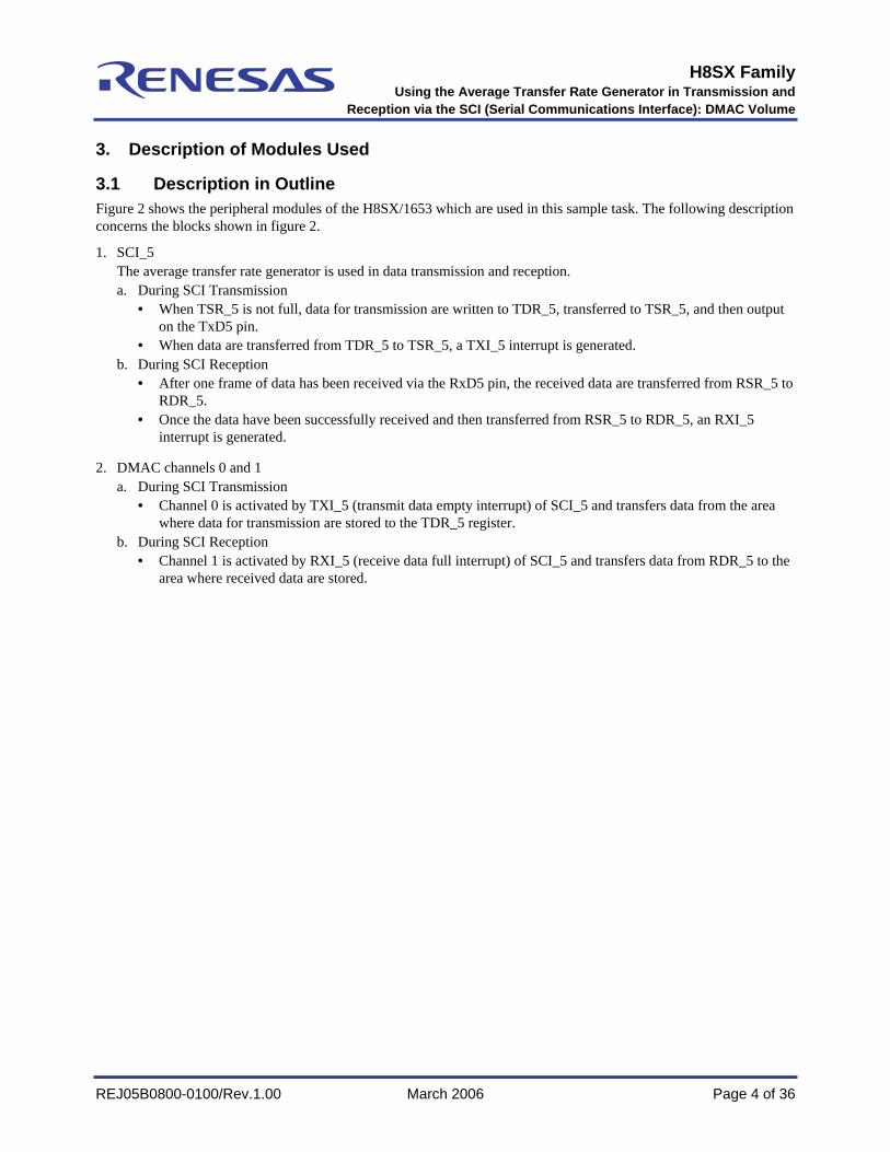
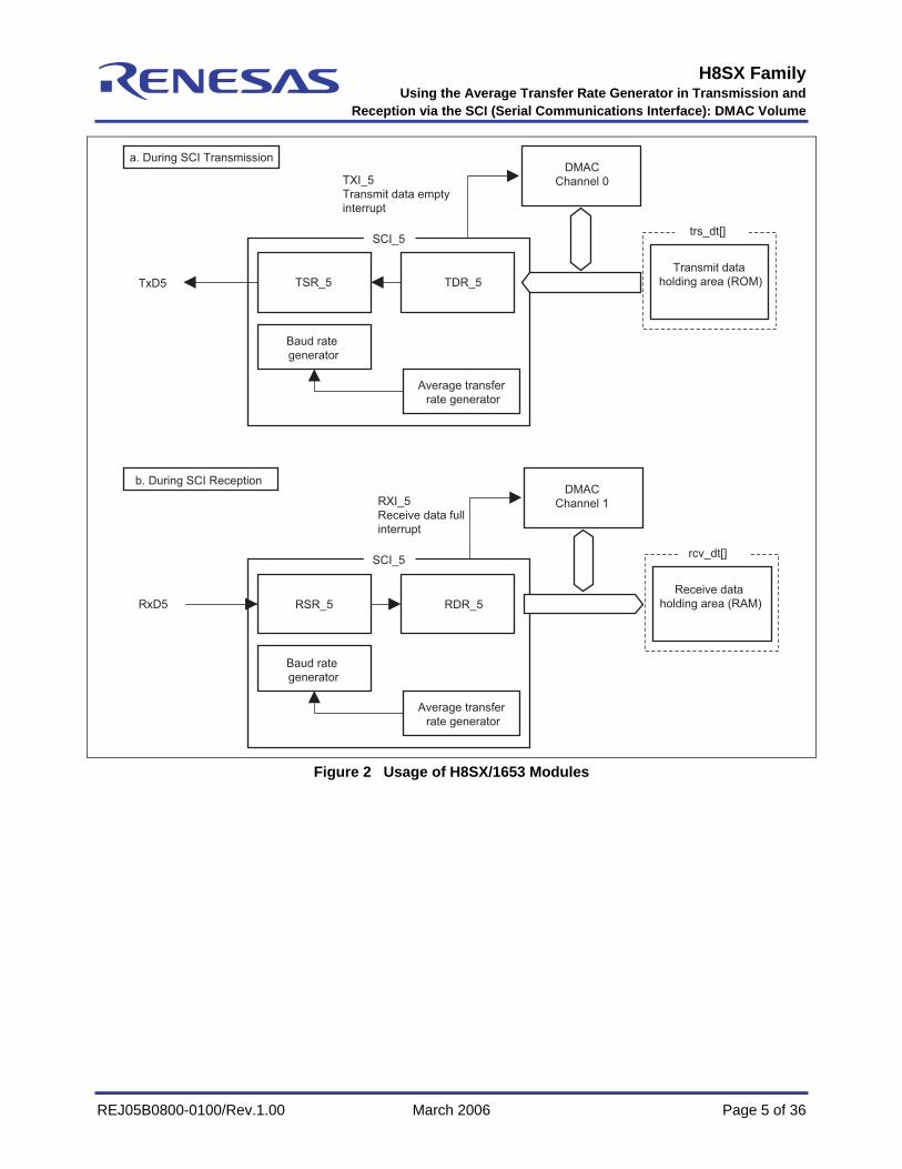
3.1 Description in Outline Figure 2 shows the peripheral modules of the H8SX/1653 which are used in this sample task. The following description concerns the blocks shown in figure 2.
1. SCI_5 The average transfer rate generator is used in data transmission and reception. a. During SCI Transmission
• When TSR_5 is not full, data for transmission are written to TDR_5, transferred to TSR_5, and then output on the TxD5 pin.
• When data are transferred from TDR_5 to TSR_5, a TXI_5 interrupt is generated. b. During SCI Reception
• After one frame of data has been received via the RxD5 pin, the received data are transferred from RSR_5 to RDR_5.
• Once the data have been successfully received and then transferred from RSR_5 to RDR_5, an RXI_5 interrupt is generated.
2. DMAC channels 0 and 1
a. During SCI Transmission • Channel 0 is activated by TXI_5 (transmit data empty interrupt) of SCI_5 and transfers data from the area
where data for transmission are stored to the TDR_5 register. b. During SCI Reception
• Channel 1 is activated by RXI_5 (receive data full interrupt) of SCI_5 and transfers data from RDR_5 to the area where received data are stored.
H8SX Family
Using the Average Transfer Rate Generator in Transmission and Reception via the SCI (Serial Communications Interface): DMAC Volume
REJ05B0800-0100/Rev.1.00 March 2006 Page 5 of 36
TxD5
RxD5
TSR_5 TDR_5
Baud rate
generator
Average transfer
rate generator
DMAC
Channel 0
trs_dt[]
Transmit data
holding area (ROM)
RSR_5 RDR_5
Baud rate
generator
Average transfer
rate generator
DMAC
Channel 1
rcv_dt[]
Receive data
holding area (RAM)
SCI_5
SCI_5
TXI_5
Transmit data empty
interrupt
RXI_5
Receive data full
interrupt
a. During SCI Transmission
b. During SCI Reception
Figure 2 Usage of H8SX/1653 Modules
H8SX Family
Using the Average Transfer Rate Generator in Transmission and Reception via the SCI (Serial Communications Interface): DMAC Volume
REJ05B0800-0100/Rev.1.00 March 2006 Page 6 of 36
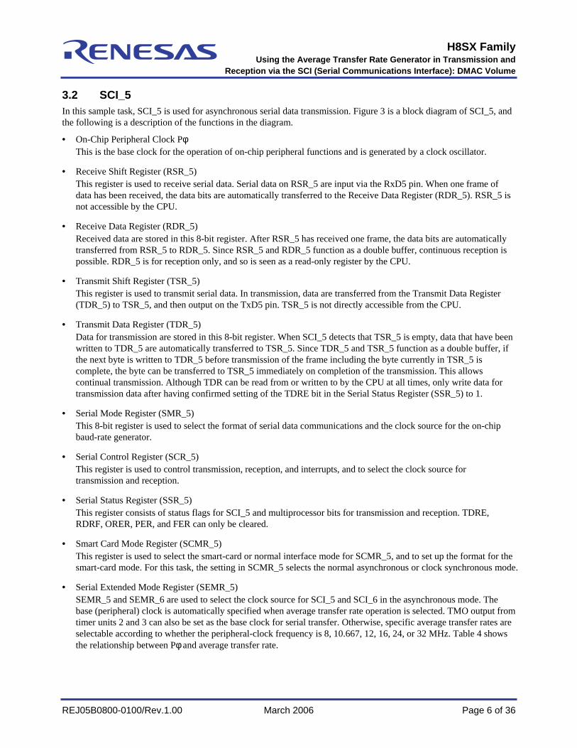
3.2 SCI_5 In this sample task, SCI_5 is used for asynchronous serial data transmission. Figure 3 is a block diagram of SCI_5, and the following is a description of the functions in the diagram.
• On-Chip Peripheral Clock Pφ This is the base clock for the operation of on-chip peripheral functions and is generated by a clock oscillator.
• Receive Shift Register (RSR_5)
This register is used to receive serial data. Serial data on RSR_5 are input via the RxD5 pin. When one frame of data has been received, the data bits are automatically transferred to the Receive Data Register (RDR_5). RSR_5 is not accessible by the CPU.
• Receive Data Register (RDR_5)
Received data are stored in this 8-bit register. After RSR_5 has received one frame, the data bits are automatically transferred from RSR_5 to RDR_5. Since RSR_5 and RDR_5 function as a double buffer, continuous reception is possible. RDR_5 is for reception only, and so is seen as a read-only register by the CPU.
• Transmit Shift Register (TSR_5)
This register is used to transmit serial data. In transmission, data are transferred from the Transmit Data Register (TDR_5) to TSR_5, and then output on the TxD5 pin. TSR_5 is not directly accessible from the CPU.
• Transmit Data Register (TDR_5)
Data for transmission are stored in this 8-bit register. When SCI_5 detects that TSR_5 is empty, data that have been written to TDR_5 are automatically transferred to TSR_5. Since TDR_5 and TSR_5 function as a double buffer, if the next byte is written to TDR_5 before transmission of the frame including the byte currently in TSR_5 is complete, the byte can be transferred to TSR_5 immediately on completion of the transmission. This allows continual transmission. Although TDR can be read from or written to by the CPU at all times, only write data for transmission data after having confirmed setting of the TDRE bit in the Serial Status Register (SSR_5) to 1.
• Serial Mode Register (SMR_5)
This 8-bit register is used to select the format of serial data communications and the clock source for the on-chip baud-rate generator.
• Serial Control Register (SCR_5)
This register is used to control transmission, reception, and interrupts, and to select the clock source for transmission and reception.
• Serial Status Register (SSR_5)
This register consists of status flags for SCI_5 and multiprocessor bits for transmission and reception. TDRE, RDRF, ORER, PER, and FER can only be cleared.
• Smart Card Mode Register (SCMR_5)
This register is used to select the smart-card or normal interface mode for SCMR_5, and to set up the format for the smart-card mode. For this task, the setting in SCMR_5 selects the normal asynchronous or clock synchronous mode.
• Serial Extended Mode Register (SEMR_5)
SEMR_5 and SEMR_6 are used to select the clock source for SCI_5 and SCI_6 in the asynchronous mode. The base (peripheral) clock is automatically specified when average transfer rate operation is selected. TMO output from timer units 2 and 3 can also be set as the base clock for serial transfer. Otherwise, specific average transfer rates are selectable according to whether the peripheral-clock frequency is 8, 10.667, 12, 16, 24, or 32 MHz. Table 4 shows the relationship between Pφ and average transfer rate.
H8SX Family
Using the Average Transfer Rate Generator in Transmission and Reception via the SCI (Serial Communications Interface): DMAC Volume
REJ05B0800-0100/Rev.1.00 March 2006 Page 7 of 36
Pφ
SCI_5
Setting of transfer rate
Baud rate generator
Average transfer rate generator*1
Clock
Transmission and
reception control
SEMR_5
Serial Extended Mode Register_5
SSR_5
Serial Status Register_5
SCR_5
Serial Control Register_5
SMR_5
Serial Mode Register_5
SCMR_5
Smart Card Mode Register_5
TSR_5
Transmit Shift Register_5
RSR_5
Receive Shift Register_5
TDR_5
Transmit Data Register_5
RDR_5
Receive Data Register_5
TxD5
RxD5
TMR unit 2
Interrupt requests
TEI_5
TXI_5
RXI_5
ERI_5
*1: Example of transfer rate for a given peripheral clock frequency
Operation at 16 MHz: 921.569 kbps
Figure 3 SCI_5 Block Diagram
Table 4 Transfer Rates of Average Transfer Rate Generators on SCI_5 and 6
Pφ (MHz) Average Transfer Rate (kbps) 8 460.784 10.667 115.152
460.606 12 230.263
460.526 16 115.196
460.784 720 921.569
24 115.132 460.526 720 921.053
32 720
H8SX Family
Using the Average Transfer Rate Generator in Transmission and Reception via the SCI (Serial Communications Interface): DMAC Volume
REJ05B0800-0100/Rev.1.00 March 2006 Page 8 of 36
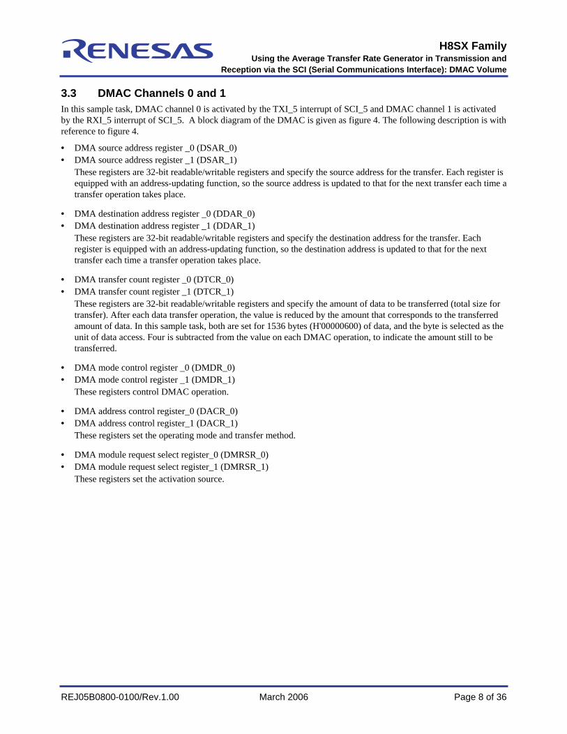
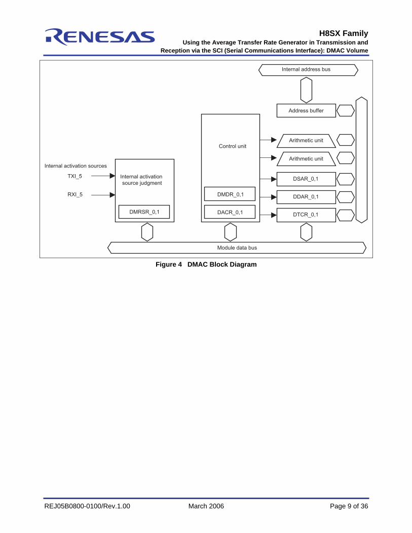
3.3 DMAC Channels 0 and 1 In this sample task, DMAC channel 0 is activated by the TXI_5 interrupt of SCI_5 and DMAC channel 1 is activated by the RXI_5 interrupt of SCI_5. A block diagram of the DMAC is given as figure 4. The following description is with reference to figure 4.
• DMA source address register _0 (DSAR_0) • DMA source address register _1 (DSAR_1)
These registers are 32-bit readable/writable registers and specify the source address for the transfer. Each register is equipped with an address-updating function, so the source address is updated to that for the next transfer each time a transfer operation takes place.
• DMA destination address register _0 (DDAR_0) • DMA destination address register _1 (DDAR_1)
These registers are 32-bit readable/writable registers and specify the destination address for the transfer. Each register is equipped with an address-updating function, so the destination address is updated to that for the next transfer each time a transfer operation takes place.
• DMA transfer count register _0 (DTCR_0) • DMA transfer count register _1 (DTCR_1)
These registers are 32-bit readable/writable registers and specify the amount of data to be transferred (total size for transfer). After each data transfer operation, the value is reduced by the amount that corresponds to the transferred amount of data. In this sample task, both are set for 1536 bytes (H'00000600) of data, and the byte is selected as the unit of data access. Four is subtracted from the value on each DMAC operation, to indicate the amount still to be transferred.
• DMA mode control register _0 (DMDR_0) • DMA mode control register _1 (DMDR_1)
These registers control DMAC operation. • DMA address control register_0 (DACR_0) • DMA address control register_1 (DACR_1)
These registers set the operating mode and transfer method. • DMA module request select register_0 (DMRSR_0) • DMA module request select register_1 (DMRSR_1)
These registers set the activation source.
H8SX Family
Using the Average Transfer Rate Generator in Transmission and Reception via the SCI (Serial Communications Interface): DMAC Volume
REJ05B0800-0100/Rev.1.00 March 2006 Page 9 of 36
Internal address bus
Address buffer
Arithmetic unit
Arithmetic unit
DSAR_0,1
DDAR_0,1
DTCR_0,1
DMDR_0,1
DACR_0,1DMRSR_0,1
TXI_5
RXI_5
Internal activation
source judgment
Control unit
Module data bus
Internal activation sources
Figure 4 DMAC Block Diagram
H8SX Family
Using the Average Transfer Rate Generator in Transmission and Reception via the SCI (Serial Communications Interface): DMAC Volume
REJ05B0800-0100/Rev.1.00 March 2006 Page 10 of 36
4. Description of Operation
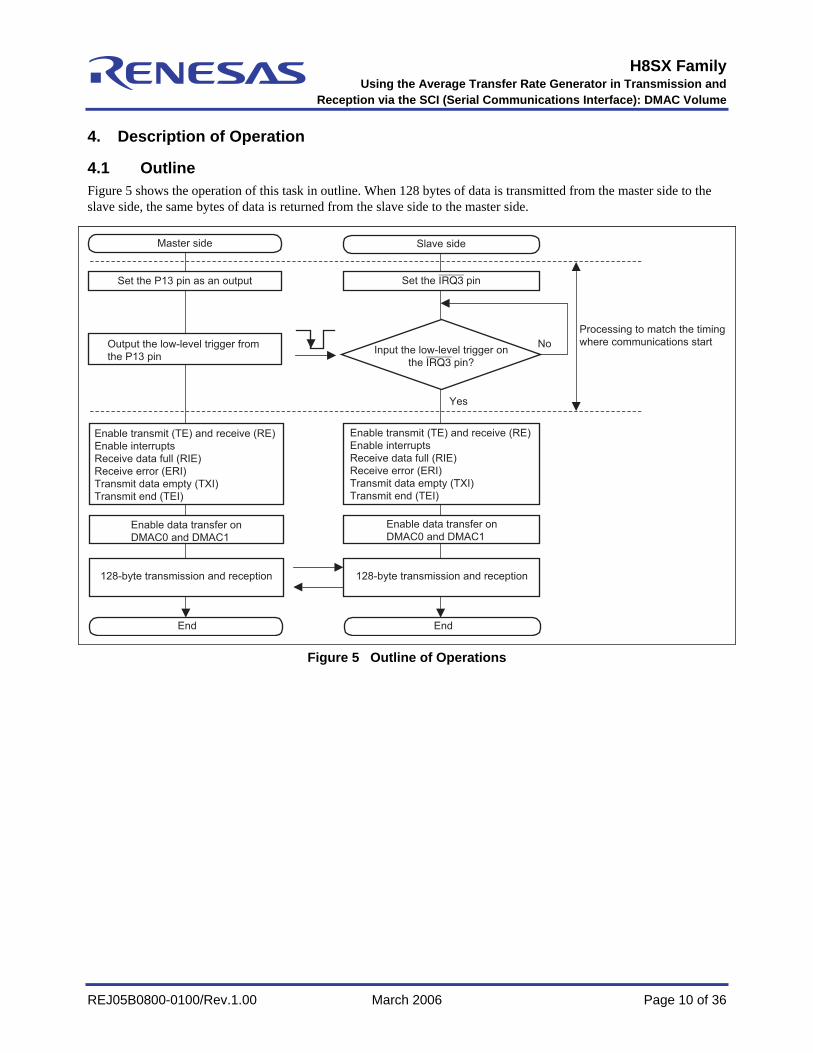
4.1 Outline Figure 5 shows the operation of this task in outline. When 128 bytes of data is transmitted from the master side to the slave side, the same bytes of data is returned from the slave side to the master side.
End End
Yes
No
Master side Slave side
Set the P13 pin as an output Set the IRQ3 pin
Input the low-level trigger on
the IRQ3 pin?
Output the low-level trigger from
the P13 pin
Processing to match the timing
where communications start
Enable transmit (TE) and receive (RE)
Enable interrupts
Receive data full (RIE)
Receive error (ERI)
Transmit data empty (TXI)
Transmit end (TEI)
Enable data transfer on
DMAC0 and DMAC1
Enable transmit (TE) and receive (RE)
Enable interrupts
Receive data full (RIE)
Receive error (ERI)
Transmit data empty (TXI)
Transmit end (TEI)
Enable data transfer on
DMAC0 and DMAC1
128-byte transmission and reception 128-byte transmission and reception
Figure 5 Outline of Operations
H8SX Family
Using the Average Transfer Rate Generator in Transmission and Reception via the SCI (Serial Communications Interface): DMAC Volume
REJ05B0800-0100/Rev.1.00 March 2006 Page 11 of 36
4.2 Transmission The timing of transmission operations is shown in figure 6. Table 5 is a list of the hardware and software processing at the numbered points in figure 6.
0 D0 D1 D2 D3 D4 D5 D6 D7 1 01D7 1D0 D1 D2 D3 D4 D5 D6 D7
(1)
0
128128
0
(2) (1) (3) (4)
TxD5
TDRE
TEND
Bus cycle
DMAC0
DTE_0
DTCR_0
DTIF_0
126th byte 127th byte 128th byte
Stop bit Stop bit Stop bit
Start bit Start bit
DM0 DM0
Figure 6 Timing of Transmission
Table 5 Processing
Hardware Processing Software Processing (1) a. Set TDRE to 1.
b. Activate DMAC_0, and transfer data for transmission from RAM to TDR_5. c. Clear TDRE to 0.
None
(2) a. Decrement DTCR_0. b. Transfer the contents of TDR_5 to TSR_5. c. Output the contents of TSR_5 on the TxD5 pin.
None
(3) a. Decrement DTCR_0 (producing DTCR_0 = 0). b. Transfer the contents of TDR_5 to TSR_5. c. Output the contents of TSR_5 on the TxD5 pin.
DMA transfer end interrupt processing a. Disable transmission and transmit end interrupts.
(4) a. Set TEND to 1. TEI interrupt processing a. Clear TE to 0. b. Disable TEI interrupts.
H8SX Family
Using the Average Transfer Rate Generator in Transmission and Reception via the SCI (Serial Communications Interface): DMAC Volume
REJ05B0800-0100/Rev.1.00 March 2006 Page 12 of 36
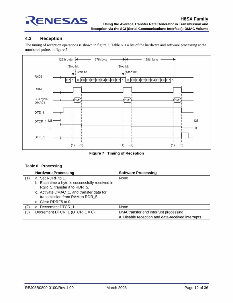
4.3 Reception The timing of reception operations is shown in figure 7. Table 6 is a list of the hardware and software processing at the numbered points in figure 7.
0
128128
0
0 D0 D1 D2 D3 D4 D5 D6 D7 1 01D7 1D0 D1 D2 D3 D4 D5 D6 D7
(1) (2) (1) (2) (1) (3)
DM1DM1DM1
126th byte 127th byte 128th byte
RxD5
RDRF
Bus cycle
DMAC1
DTCR_1
DTE_1
DTIF_1
Stop bit
Start bit Start bit
Stop bit
Figure 7 Timing of Reception
Table 6 Processing
Hardware Processing Software Processing (1) a. Set RDRF to 1.
b. Each time a byte is successfully received in RSR_5, transfer it to RDR_5. c. Activate DMAC_1, and transfer data for transmission from RAM to RDR_5. d. Clear RDRF5 to 0.
None
(2) a. Decrement DTCR_1. None (3) Decrement DTCR_1 (DTCR_1 = 0). DMA transfer end interrupt processing
a. Disable reception and data-received interrupts.
H8SX Family
Using the Average Transfer Rate Generator in Transmission and Reception via the SCI (Serial Communications Interface): DMAC Volume
REJ05B0800-0100/Rev.1.00 March 2006 Page 13 of 36
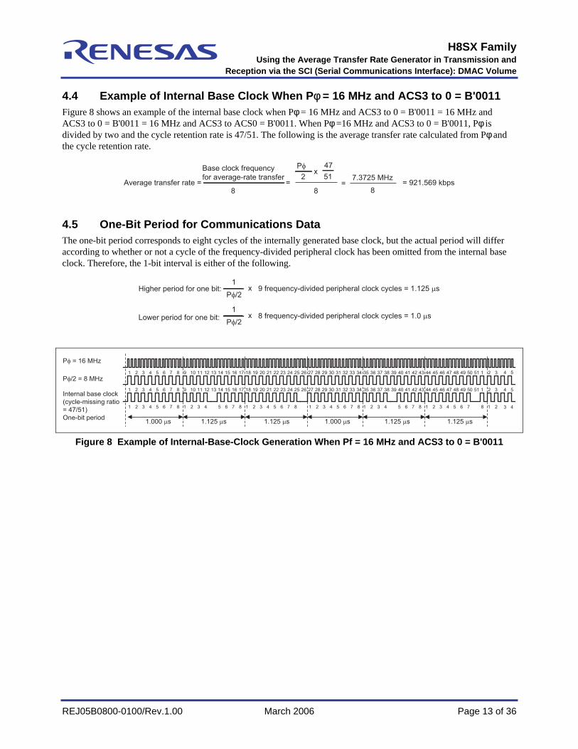
4.4 Example of Internal Base Clock When Pφ = 16 MHz and ACS3 to 0 = B'0011 Figure 8 shows an example of the internal base clock when Pφ = 16 MHz and ACS3 to 0 = B'0011 = 16 MHz and ACS3 to 0 = B'0011 = 16 MHz and ACS3 to ACS0 = B'0011. When Pφ =16 MHz and ACS3 to 0 = B'0011, Pφ is divided by two and the cycle retention rate is 47/51. The following is the average transfer rate calculated from Pφ and the cycle retention rate.
Average transfer rate =8
Base clock frequency
for average-rate transfer= = 921.569 kbps
8
7.3725 MHz
Pφ
2x
51
47
=8
4.5 One-Bit Period for Communications Data The one-bit period corresponds to eight cycles of the internally generated base clock, but the actual period will differ according to whether or not a cycle of the frequency-divided peripheral clock has been omitted from the internal base clock. Therefore, the 1-bit interval is either of the following.
Higher period for one bit: Pφ/2
1x 9 frequency-divided peripheral clock cycles = 1.125 µs
Lower period for one bit: Pφ/2
1x 8 frequency-divided peripheral clock cycles = 1.0 µs
4 5
4 5
3 4
1 2 3 4 5 6 7 8 9 10 11 12 13 14 15 16 17 18 19 20 21 22 23 24 25 26 27 28 29 30 31 32 33 34 35 36 37 38 39 40 41 42 43 44 45 46 47 48 49 50 51 1 2
1 2 3 4 5 6 7 8 9 10 11 12 13 14 15 16 17 18 19 20 21 22 23 24 25 26 27 28 29 30 31 32 33 34 35 36 37 38 39 40 41 42 43 44 45 46 47 48 49 50 51 1 2 3
1 2 3 4 5 6 7 8 1 2 3 4 5 6 7 81 2 3 4 5 6 7 8 1 2 3 4 5 6 7 8 1 2 3 4 5 6 7 8 1 2 3 4 5 6 7 8 1 2
3
1.000 µs 1.125 µs 1.125 µs 1.000 µs 1.125 µs 1.125 µs
Pφ = 16 MHz
Pφ/2 = 8 MHz
Internal base clock
(cycle-missing ratio
= 47/51)
One-bit period
Figure 8 Example of Internal-Base-Clock Generation When Pf = 16 MHz and ACS3 to 0 = B'0011
H8SX Family
Using the Average Transfer Rate Generator in Transmission and Reception via the SCI (Serial Communications Interface): DMAC Volume
REJ05B0800-0100/Rev.1.00 March 2006 Page 14 of 36
5. Description of Software
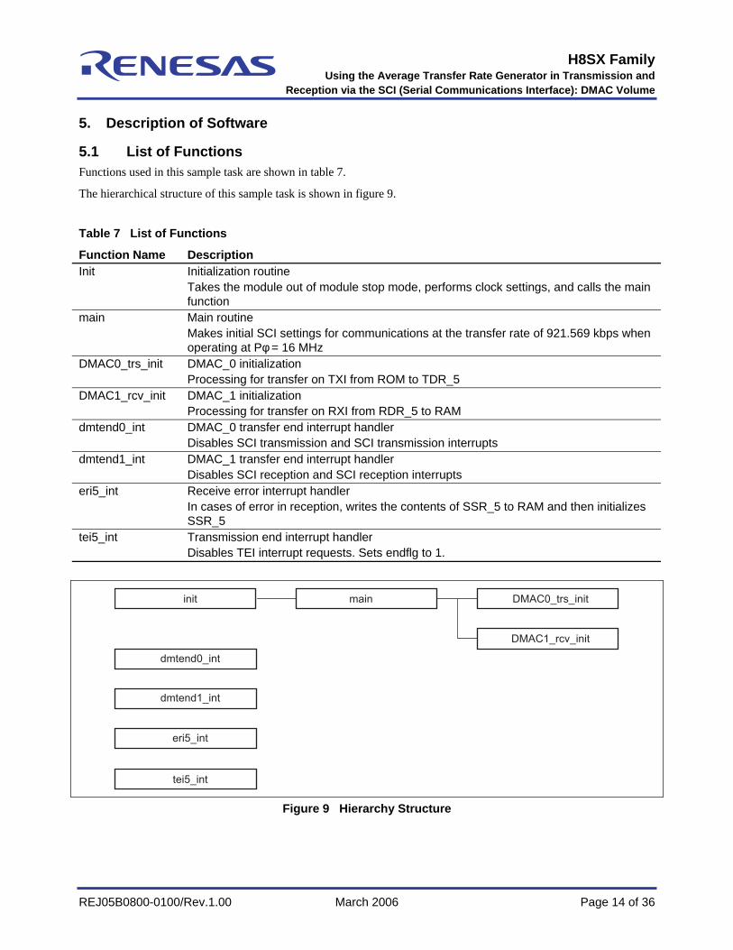
5.1 List of Functions Functions used in this sample task are shown in table 7.
The hierarchical structure of this sample task is shown in figure 9.
Table 7 List of Functions
Function Name Description Init Initialization routine
Takes the module out of module stop mode, performs clock settings, and calls the main function
main Main routine Makes initial SCI settings for communications at the transfer rate of 921.569 kbps when operating at Pφ = 16 MHz
DMAC0_trs_init DMAC_0 initialization Processing for transfer on TXI from ROM to TDR_5
DMAC1_rcv_init DMAC_1 initialization Processing for transfer on RXI from RDR_5 to RAM
dmtend0_int DMAC_0 transfer end interrupt handler Disables SCI transmission and SCI transmission interrupts
dmtend1_int DMAC_1 transfer end interrupt handler Disables SCI reception and SCI reception interrupts
eri5_int Receive error interrupt handler In cases of error in reception, writes the contents of SSR_5 to RAM and then initializes SSR_5
tei5_int Transmission end interrupt handler Disables TEI interrupt requests. Sets endflg to 1.
init main DMAC0_trs_init
DMAC1_rcv_init
dmtend0_int
dmtend1_int
eri5_int
tei5_int
Figure 9 Hierarchy Structure
H8SX Family
Using the Average Transfer Rate Generator in Transmission and Reception via the SCI (Serial Communications Interface): DMAC Volume
REJ05B0800-0100/Rev.1.00 March 2006 Page 15 of 36
5.2 Vector Table Table 8 Exception Handling Vector Table
Exception Handling Source
Vector Number
Address in Vector Table
Vector Table Address Handling Function
Reset 0 H'000000 Init DMAC_0 DMTEND0 128 H'000200 dmtend0_int DMAC_1 DMTEND1 129 H'000204 dmtend1_int SCI_5 ERI5 222 H'000378 eri5_init SCI_5 TEI5 223 H'00037C tei5_init
5.3 RAM Usage Table 9 RAM Usage
Type Variable Name Contents Used In unsigned char endflg Transmission end flag
0: Transmission in progress 1: Transmission ended
main, tei5_int
unsigned char errbuf Reception error buffer The contents of SSR_5 are stored here when an overrun error, flaming error, or parity error occurs.
main, eri5_int
unsigned char tcnt Transmission counter main, txi5_int unsigned char rcnt Reception counter main, rxi5_int unsigned char rcv_dt[128] RAM area for storing received data main, rxi5_int
5.4 Data Table Table 10 Data Table
Type Variable Name Contents Used In unsigned char trs_dt[128] ROM area where data for transmission are
stored. 128 bytes of data: H'00, H'01, …, H'7F
main, txi5_int
5.5 Defined Macros Table 11 Defined Macros
Identifier Contents Used In MASTER If this is defined, compilation generates the master-side program. main SLAVE If this is defined, compilation generates the slave-side program. main
H8SX Family
Using the Average Transfer Rate Generator in Transmission and Reception via the SCI (Serial Communications Interface): DMAC Volume
REJ05B0800-0100/Rev.1.00 March 2006 Page 16 of 36
5.6 Description of Functions 5.6.1 init Function 1. Overview
Initialization routine. Takes the module out of module stopped mode, sets the clock, and calls the main function. 2. Arguments
None 3. Return value
None 4. Description of internal register usage
Usage of internal registers in this task is described below. The given settings are those used in the task and differ from the initial settings.
• System Clock Control Register (SCKCR) Address: H'FFFDC4 Bit Bit Name Setting R/W Description 10 9 8
ICK2 ICK1 ICK0
0 1 0
R/W R/W R/W
System clock (Iφ) select Selects the frequency of the CPU, DMAC, DTC module and system clock 010: Input clock x 1
6 5 4
PCK2 PCK1 PCK0
0 1 0
R/W R/W R/W
Peripheral module clock (Pφ) select Selects the frequency of peripheral module clock 010: Input clock x 1
2 1 0
BCK2 BCK1 BCK0
0 1 0
R/W R/W R/W
External bus clock (Bφ) selection Selects the frequency of the external bus clock 010: Input clock x 1
• Registers MSTPCRA, MSTPCRB, and MSTPCRC control the module stop mode. Setting a bit to 1 makes the
corresponding module enter the module stop mode, while clearing the bit to 0 takes the module out of stop mode. • Module Stop Control Register A (MSTPCRA) Address: H'FFFDC8 Bit Bit Name Setting R/W Description 15 ACSE 0 R/W All-Module-Clock-Stop Mode Enable
Enables/disables all-module-clock-stop mode for reducing current drawn by stopping the bus controller and I/O port operations when the CPU executes the SLEEP instruction after the module stop mode has been set for all the on-chip peripheral modules controlled by MSTPCR 0: All-module-clock-stop mode disabled 1: All-module-clock-stop mode enabled
13 MSTPA13 1 R/W DMA controller (DMAC) 12 MSTPA12 1 R/W Data transfer controller (DTC) 9 MSTPA9 1 R/W 8-bit timers (TMR_3, TMR_2) 8 MSTPA8 1 R/W 8-bit timers (TMR_1, TMR_0) 5 MSTPA5 1 R/W D/A converter channels 1, 0 3 MSTPA3 1 R/W A/D converter (unit 0) 0 MSTPA0 1 R/W 16-bit timer pulse unit (TPU channels 5 to 0)
H8SX Family
Using the Average Transfer Rate Generator in Transmission and Reception via the SCI (Serial Communications Interface): DMAC Volume
REJ05B0800-0100/Rev.1.00 March 2006 Page 17 of 36
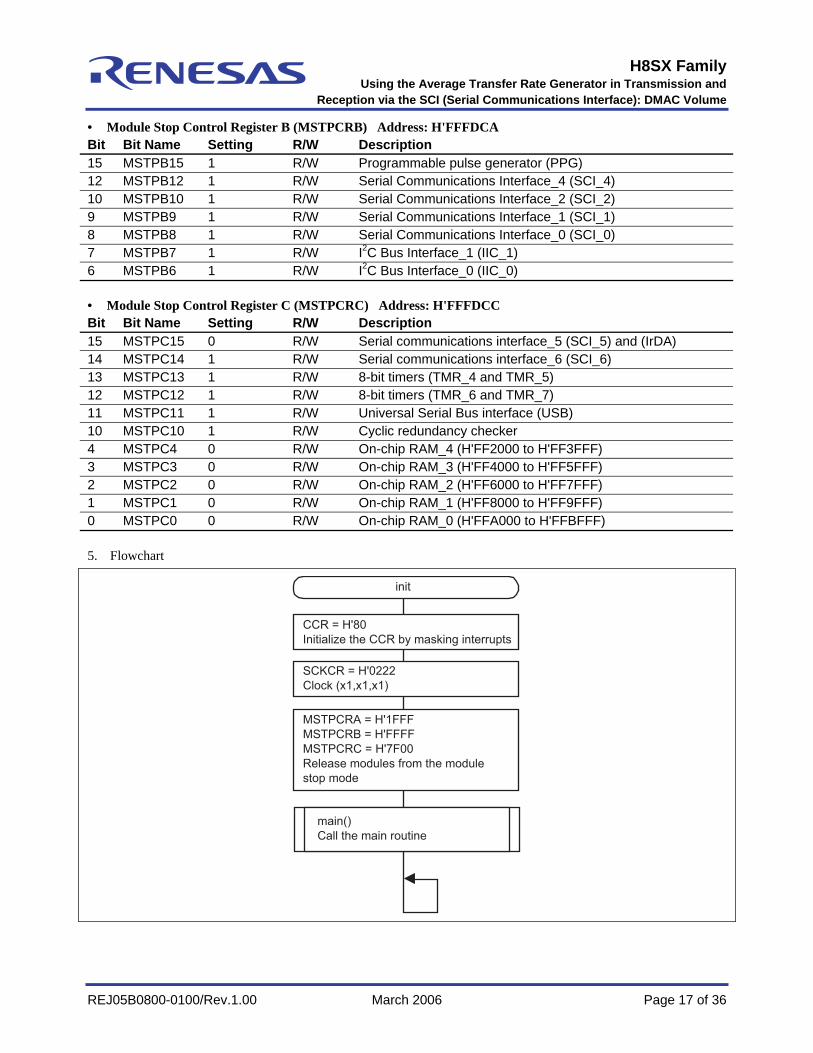
• Module Stop Control Register B (MSTPCRB) Address: H'FFFDCA Bit Bit Name Setting R/W Description 15 MSTPB15 1 R/W Programmable pulse generator (PPG) 12 MSTPB12 1 R/W Serial Communications Interface_4 (SCI_4) 10 MSTPB10 1 R/W Serial Communications Interface_2 (SCI_2) 9 MSTPB9 1 R/W Serial Communications Interface_1 (SCI_1) 8 MSTPB8 1 R/W Serial Communications Interface_0 (SCI_0) 7 MSTPB7 1 R/W I2C Bus Interface_1 (IIC_1) 6 MSTPB6 1 R/W I2C Bus Interface_0 (IIC_0) • Module Stop Control Register C (MSTPCRC) Address: H'FFFDCC Bit Bit Name Setting R/W Description 15 MSTPC15 0 R/W Serial communications interface_5 (SCI_5) and (IrDA) 14 MSTPC14 1 R/W Serial communications interface_6 (SCI_6) 13 MSTPC13 1 R/W 8-bit timers (TMR_4 and TMR_5) 12 MSTPC12 1 R/W 8-bit timers (TMR_6 and TMR_7) 11 MSTPC11 1 R/W Universal Serial Bus interface (USB) 10 MSTPC10 1 R/W Cyclic redundancy checker 4 MSTPC4 0 R/W On-chip RAM_4 (H'FF2000 to H'FF3FFF) 3 MSTPC3 0 R/W On-chip RAM_3 (H'FF4000 to H'FF5FFF) 2 MSTPC2 0 R/W On-chip RAM_2 (H'FF6000 to H'FF7FFF) 1 MSTPC1 0 R/W On-chip RAM_1 (H'FF8000 to H'FF9FFF) 0 MSTPC0 0 R/W On-chip RAM_0 (H'FFA000 to H'FFBFFF) 5. Flowchart
init
CCR = H'80
Initialize the CCR by masking interrupts
SCKCR = H'0222
Clock (x1,x1,x1)
MSTPCRA = H'1FFF
MSTPCRB = H'FFFF
MSTPCRC = H'7F00
Release modules from the module
stop mode
main()
Call the main routine
H8SX Family
Using the Average Transfer Rate Generator in Transmission and Reception via the SCI (Serial Communications Interface): DMAC Volume
REJ05B0800-0100/Rev.1.00 March 2006 Page 18 of 36
5.6.2 main Function 1. Overview
Main routine. Sets the average transfer rate in SCI, makes DMAC0_trs_init function and DMAC1_rcv_init function calls, transmits and receives a total of 256 bytes of data.
2. Arguments None
3. Return value None
4. Description of internal register usage Usage of internal registers in this task is described below. The given settings are those used in the task and differ from the initial settings.
• Port 1 Data Direction Register (P1DDR) Address: H'FFFB80 Bit Bit Name Setting R/W Description 3 P13DDR 1 W 0: P13 pin is an input
1: P13 pin is an output • Port 1 Input Buffer Control Register (P1ICR) Address: H'FFFB90 Bit Bit Name Setting R/W Description 5 P15ICR 1 R/W 0: P15 pin input buffer is disabled. Input signal is fixed to the
high level. 1: P15 pin input buffer is valid. The pin state reflects the peripheral modules.
3 P13ICR 1 R/W 0: P13 pin input buffer is disabled. Input signal is fixed to the high level. 1: P13 pin input buffer is valid. The pin state reflects the peripheral modules.
• Port Function Control Register (PFCRC) Address: H'FFFBCC Bit Bit Name Setting R/W Description 3 ITS3 1 R/W IRQ3 Pin Select
0: Selects IRQ3-A input on pin P13 1: Selects IRQ3-B input on pin P53
• IRQ Sense Control Register L (ISCRL) Address: H'FFFD6A Bit Bit Name Setting R/W Description 7 6
IRQ3SR IRQ3SF
0 1
R/W R/W
IRQ3 Sense Control Rise IRQ3 Sense Control Fall 01: Interrupt requests are sensed on falling edges of IRQ3 input
H8SX Family
Using the Average Transfer Rate Generator in Transmission and Reception via the SCI (Serial Communications Interface): DMAC Volume
REJ05B0800-0100/Rev.1.00 March 2006 Page 19 of 36
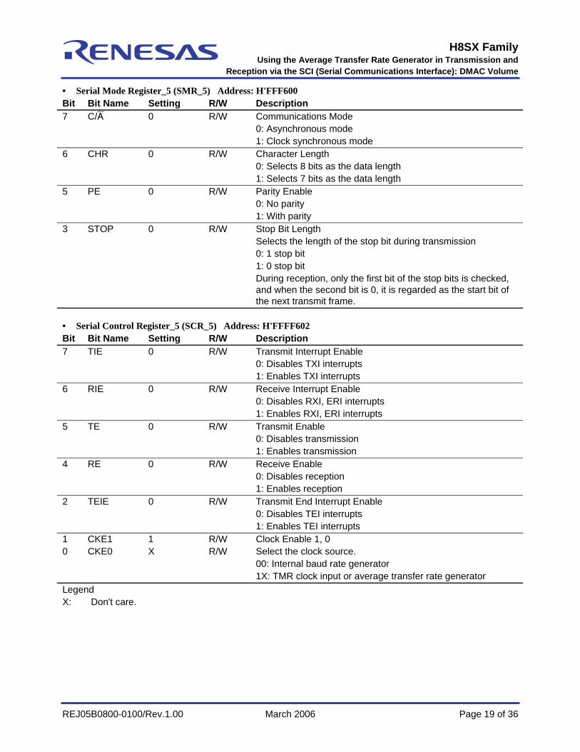
• Serial Mode Register_5 (SMR_5) Address: H'FFF600 Bit Bit Name Setting R/W Description 7 C/A 0 R/W Communications Mode
0: Asynchronous mode 1: Clock synchronous mode
6 CHR 0 R/W Character Length 0: Selects 8 bits as the data length 1: Selects 7 bits as the data length
5 PE 0 R/W Parity Enable 0: No parity 1: With parity
3 STOP 0 R/W Stop Bit Length Selects the length of the stop bit during transmission 0: 1 stop bit 1: 0 stop bit During reception, only the first bit of the stop bits is checked, and when the second bit is 0, it is regarded as the start bit of the next transmit frame.
• Serial Control Register_5 (SCR_5) Address: H'FFFF602 Bit Bit Name Setting R/W Description 7 TIE 0 R/W Transmit Interrupt Enable
0: Disables TXI interrupts 1: Enables TXI interrupts
6 RIE 0 R/W Receive Interrupt Enable 0: Disables RXI, ERI interrupts 1: Enables RXI, ERI interrupts
5 TE 0 R/W Transmit Enable 0: Disables transmission 1: Enables transmission
4 RE 0 R/W Receive Enable 0: Disables reception 1: Enables reception
2 TEIE 0 R/W Transmit End Interrupt Enable 0: Disables TEI interrupts 1: Enables TEI interrupts
1 0
CKE1 CKE0
1 X
R/W R/W
Clock Enable 1, 0 Select the clock source. 00: Internal baud rate generator 1X: TMR clock input or average transfer rate generator
Legend X: Don't care.
H8SX Family
Using the Average Transfer Rate Generator in Transmission and Reception via the SCI (Serial Communications Interface): DMAC Volume
REJ05B0800-0100/Rev.1.00 March 2006 Page 20 of 36
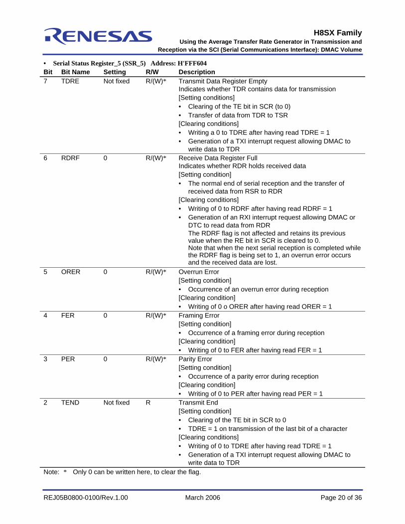
• Serial Status Register_5 (SSR_5) Address: H'FFF604 Bit Bit Name Setting R/W Description 7 TDRE Not fixed R/(W)* Transmit Data Register Empty
Indicates whether TDR contains data for transmission [Setting conditions] • Clearing of the TE bit in SCR (to 0) • Transfer of data from TDR to TSR [Clearing conditions] • Writing a 0 to TDRE after having read TDRE = 1 • Generation of a TXI interrupt request allowing DMAC to
write data to TDR 6 RDRF 0 R/(W)* Receive Data Register Full
Indicates whether RDR holds received data [Setting condition] • The normal end of serial reception and the transfer of
received data from RSR to RDR [Clearing conditions] • Writing of 0 to RDRF after having read RDRF = 1 • Generation of an RXI interrupt request allowing DMAC or
DTC to read data from RDR The RDRF flag is not affected and retains its previous value when the RE bit in SCR is cleared to 0. Note that when the next serial reception is completed while the RDRF flag is being set to 1, an overrun error occurs and the received data are lost.
5 ORER 0 R/(W)* Overrun Error [Setting condition] • Occurrence of an overrun error during reception [Clearing condition] • Writing of 0 o ORER after having read ORER = 1
4 FER 0 R/(W)* Framing Error [Setting condition] • Occurrence of a framing error during reception [Clearing condition] • Writing of 0 to FER after having read FER = 1
3 PER 0 R/(W)* Parity Error [Setting condition] • Occurrence of a parity error during reception [Clearing condition] • Writing of 0 to PER after having read PER = 1
2 TEND Not fixed R Transmit End [Setting condition] • Clearing of the TE bit in SCR to 0 • TDRE = 1 on transmission of the last bit of a character [Clearing conditions] • Writing of 0 to TDRE after having read TDRE = 1 • Generation of a TXI interrupt request allowing DMAC to
write data to TDR Note: * Only 0 can be written here, to clear the flag.
H8SX Family
Using the Average Transfer Rate Generator in Transmission and Reception via the SCI (Serial Communications Interface): DMAC Volume
REJ05B0800-0100/Rev.1.00 March 2006 Page 21 of 36
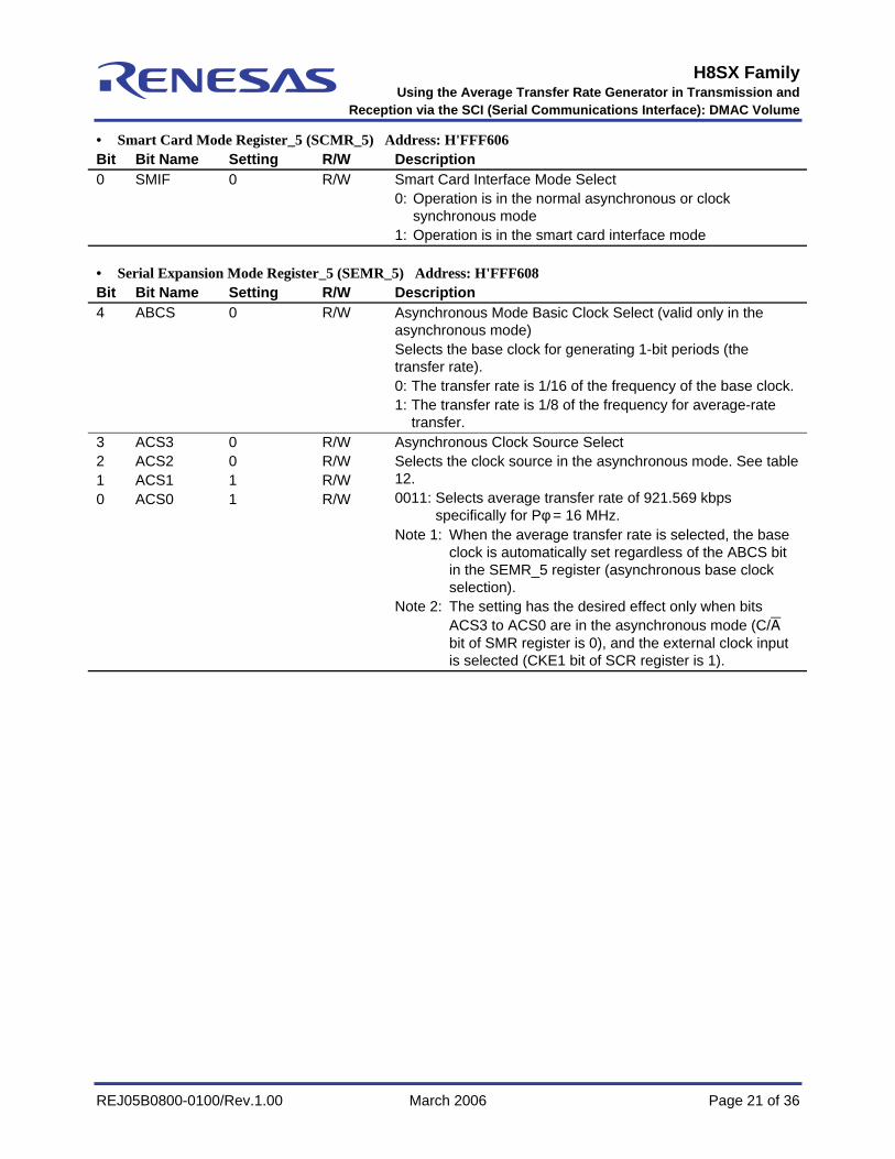
• Smart Card Mode Register_5 (SCMR_5) Address: H'FFF606 Bit Bit Name Setting R/W Description 0 SMIF 0 R/W Smart Card Interface Mode Select
0: Operation is in the normal asynchronous or clock synchronous mode 1: Operation is in the smart card interface mode
• Serial Expansion Mode Register_5 (SEMR_5) Address: H'FFF608 Bit Bit Name Setting R/W Description 4 ABCS 0 R/W Asynchronous Mode Basic Clock Select (valid only in the
asynchronous mode) Selects the base clock for generating 1-bit periods (the transfer rate). 0: The transfer rate is 1/16 of the frequency of the base clock.1: The transfer rate is 1/8 of the frequency for average-rate transfer.
3 2 1 0
ACS3 ACS2 ACS1 ACS0
0 0 1 1
R/W R/W R/W R/W
Asynchronous Clock Source Select Selects the clock source in the asynchronous mode. See table 12. 0011: Selects average transfer rate of 921.569 kbps specifically for Pφ = 16 MHz. Note 1: When the average transfer rate is selected, the base
clock is automatically set regardless of the ABCS bit in the SEMR_5 register (asynchronous base clock selection).
Note 2: The setting has the desired effect only when bits ACS3 to ACS0 are in the asynchronous mode (C/A bit of SMR register is 0), and the external clock input is selected (CKE1 bit of SCR register is 1).
H8SX Family
Using the Average Transfer Rate Generator in Transmission and Reception via the SCI (Serial Communications Interface): DMAC Volume
REJ05B0800-0100/Rev.1.00 March 2006 Page 22 of 36
Table 12 List of Setting for Asynchronous Clock Source Select
ACS3 to 0 Transfer Rate Pφ (MHz) Functions 0000 (Set by the ABCS bit) - The average rate transfer generator is not used.0001 1/16th of the base clock
frequency for average-rate transfer
10.667 Average transfer rate 115.152 kbps
0010 1/8th of the base clock frequency for average-rate transfer
10.667 Average transfer rate 460.606 kbps
16 Average transfer rate 921.569 kbps 0011 1/8th of the base clock frequency for average-rate transfer 8 Average transfer rate 460.784 kbps
0100 (Set by the ABCS bits) - Selects TMR-clock input: compare-match output of TMR provides the base clock for transfer
0101 1/16th of the base clock frequency for average-rate transfer
16 Average transfer rate 115.196 kbps
0110 1/16th of the base clock frequency for average-rate transfer
16 Average transfer rate 460.784 kbps
0111 1/8th of the base clock frequency for average-rate transfer
24 Average transfer rate 720 kbps
1000 1/16th of the base clock frequency for average-rate transfer
24 Average transfer rate 115.132 kbps
24 Average transfer rate 460.526 kbps 1001 1/16th of the base clock frequency for average-rate transfer 12 Average transfer rate 230.263 kbps
1010 1/8th of the base clock frequency for average-rate transfer
24 Average transfer rate 720 kbps
24 Average transfer rate 921.053 kbps 1011 1/8th of the base clock frequency for average-rate transfer 12 Average transfer rate 460.526 kbps
1100 1/16th of the base clock frequency for average-rate transfer
32 Average transfer rate 720 kbps
H8SX Family
Using the Average Transfer Rate Generator in Transmission and Reception via the SCI (Serial Communications Interface): DMAC Volume
REJ05B0800-0100/Rev.1.00 March 2006 Page 23 of 36
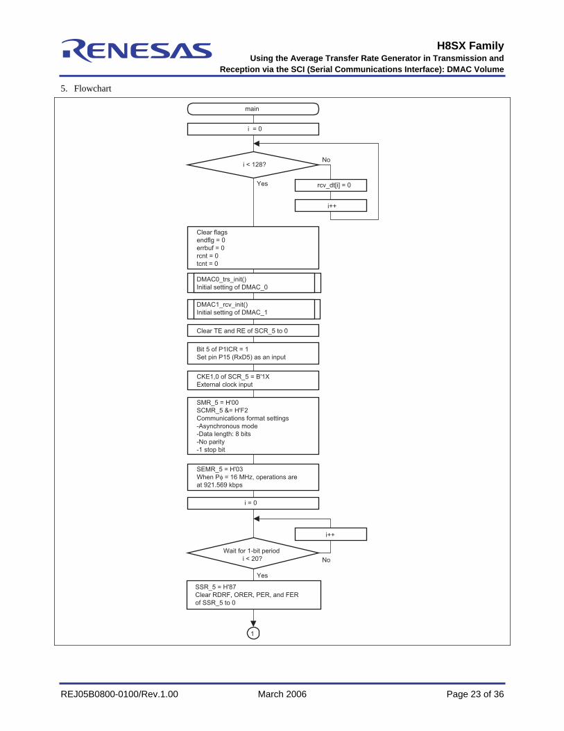
5. Flowchart
i = 0
Yes
No
i++
1
Yes
No
i = 0
i++
SSR_5 = H'87
Clear RDRF, ORER, PER, and FER
of SSR_5 to 0
Wait for 1-bit period
i < 20?
SEMR_5 = H'03
When Pφ = 16 MHz, operations are
at 921.569 kbps
SMR_5 = H'00
SCMR_5 &= H'F2
Communications format settings
-Asynchronous mode
-Data length: 8 bits
-No parity
-1 stop bit
CKE1,0 of SCR_5 = B'1X
External clock input
Bit 5 of P1ICR = 1
Set pin P15 (RxD5) as an input
Clear TE and RE of SCR_5 to 0
DMAC1_rcv_init()
Initial setting of DMAC_1
DMAC0_trs_init()
Initial setting of DMAC_0
Clear flags
endflg = 0
errbuf = 0
rcnt = 0
tcnt = 0
rcv_dt[i] = 0
i < 128?
main
H8SX Family
Using the Average Transfer Rate Generator in Transmission and Reception via the SCI (Serial Communications Interface): DMAC Volume
REJ05B0800-0100/Rev.1.00 March 2006 Page 24 of 36
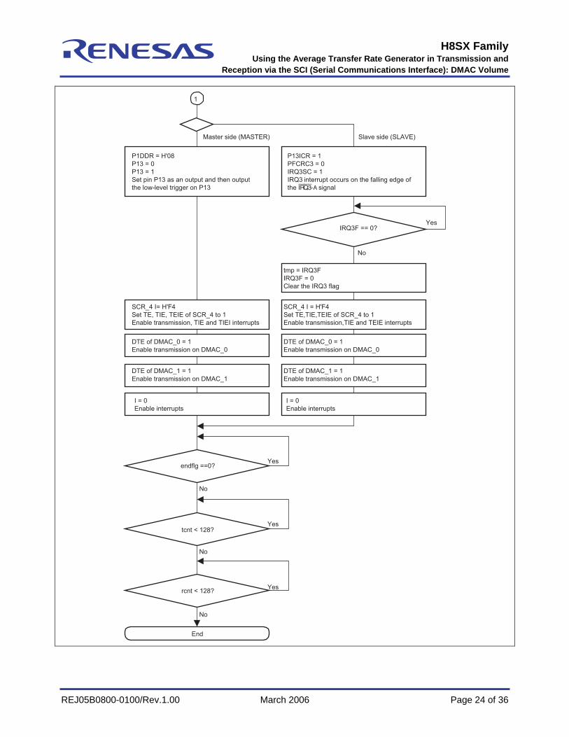
1
Yes
No
Yes
End
No
No
Yes
No
Yesrcnt < 128?
tcnt < 128?
endflg ==0?
I = 0
Enable interrupts
DTE of DMAC_1 = 1
Enable transmission on DMAC_1
DTE of DMAC_0 = 1
Enable transmission on DMAC_0
SCR_4 I= H'F4
Set TE, TIE, TEIE of SCR_4 to 1
Enable transmission, TIE and TIEI interrupts
I = 0
Enable interrupts
DTE of DMAC_1 = 1
Enable transmission on DMAC_1
DTE of DMAC_0 = 1
Enable transmission on DMAC_0
SCR_4 I = H'F4
Set TE,TIE,TEIE of SCR_4 to 1
Enable transmission,TIE and TEIE interrupts
tmp = IRQ3F
IRQ3F = 0
Clear the IRQ3 flag
P1DDR = H'08
P13 = 0
P13 = 1
Set pin P13 as an output and then output
the low-level trigger on P13
P13ICR = 1
PFCRC3 = 0
IRQ3SC = 1
IRQ3 interrupt occurs on the falling edge of
the IRQ3-A signal
Master side (MASTER) Slave side (SLAVE)
IRQ3F == 0?
H8SX Family
Using the Average Transfer Rate Generator in Transmission and Reception via the SCI (Serial Communications Interface): DMAC Volume
REJ05B0800-0100/Rev.1.00 March 2006 Page 25 of 36
5.6.3 DMAC0_trs_init Function 1. Overview
DMAC_0 initial settings. 2. Arguments
None 3. Return value
None 4. Description of internal register usage
Usage of internal registers in this task is described below. The given settings are those used in the task and differ from the initial settings.
• DMA source address register_0 (DSAR_0) Address: H'FFFC00
Function: Specifies the source address for the transfer. Setting: &trs_dt
• DMA destination address register_0 (DDAR_0) Address: H'FFFC04
Function: Specifies the destination address for the transfer. Setting: &TDR_5
• DMA transfer count register_0 (DTCR_0) Address: H'FFFC0C
Function: Selects the amount of data to be transferred as 128 bytes. Setting: 128
H8SX Family
Using the Average Transfer Rate Generator in Transmission and Reception via the SCI (Serial Communications Interface): DMAC Volume
REJ05B0800-0100/Rev.1.00 March 2006 Page 26 of 36
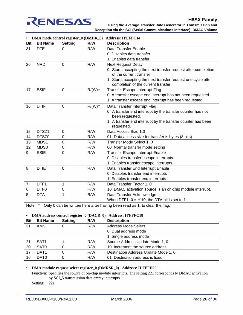
• DMA mode control register_0 (DMDR_0) Address: H'FFFC14 Bit Bit Name Setting R/W Description 31 DTE 0 R/W Data Transfer Enable
0: Disables data transfer 1: Enables data transfer
26 NRD 0 R/W Next Request Delay 0: Starts accepting the next transfer request after completion of the current transfer 1: Starts accepting the next transfer request one cycle after completion of the current transfer.
17 ESIF 0 R/(W)* Transfer Escape Interrupt Flag 0: A transfer escape end interrupt has not been requested. 1: A transfer escape end interrupt has been requested.
16 DTIF 0 R/(W)* Data Transfer Interrupt Flag 0: A transfer end interrupt by the transfer counter has not been requested. 1: A transfer end interrupt by the transfer counter has been requested.
15 14
DTSZ1 DTSZ0
0 0
R/W R/W
Data Access Size 1,0 01: Data access size for transfer is bytes (8 bits)
13 12
MDS1 MDS0
0 0
R/W R/W
Transfer Mode Select 1, 0 00: Normal transfer mode setting
9 ESIE 0 R/W Transfer Escape Interrupt Enable 0: Disables transfer escape interrupts. 1: Enables transfer escape interrupts.
8 DTIE 0 R/W Data Transfer End Interrupt Enable 0: Disables transfer end interrupts 1: Enables transfer end interrupts
7 6
DTF1 DTF0
1 0
R/W R/W
Data Transfer Factor 1, 0 10: DMAC activation source is an on-chip module interrupt.
5 DTA 1 R/W Data Transfer Acknowledge When DTF1, 0 = H'10, the DTA bit is set to 1.
Note * Only 0 can be written here after having been read as 1, to clear the flag. • DMA address control register_0 (DACR_0) Address: H'FFFC18 Bit Bit Name Setting R/W Description 31 AMS 0 R/W Address Mode Select
0: Dual address mode 1: Single address mode
21 20
SAT1 SAT0
1 0
R/W R/W
Source Address Update Mode 1, 0 10: Increment the source address
17 16
DAT1 DAT0
0 0
R/W R/W
Destination Address Update Mode 1, 0 01: Destination address is fixed
• DMA module request select register_0 (DMRSR_0) Address: H'FFFD20
Function: Specifies the source of on-chip module interrupts. The setting 221 corresponds to DMAC activation by SCI_5 transmission data empty interrupts. Setting: 221
H8SX Family
Using the Average Transfer Rate Generator in Transmission and Reception via the SCI (Serial Communications Interface): DMAC Volume
REJ05B0800-0100/Rev.1.00 March 2006 Page 27 of 36
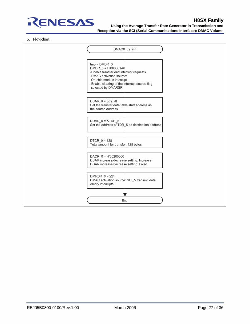
5. Flowchart
End
DMAC0_trs_init
tmp = DMDR_0
DMDR_0 = H'000001A0
-Enable transfer end interrupt requests
-DMAC activation source:
On-chip module interrupt
-Enable clearing of the interrupt source flag
selected by DMARSR
DSAR_0 = &trs_dt
Set the transfer data table start address as
the source address
DDAR_0 = &TDR_5
Set the address of TDR_5 as destination address
DTCR_0 = 128
Total amount for transfer: 128 bytes
DACR_0 = H'00200000
DSAR increase/decrease setting: Increase
DDAR increase/decrease setting: Fixed
DMRSR_0 = 221
DMAC activation source: SCI_5 transmit data
empty interrupts
H8SX Family
Using the Average Transfer Rate Generator in Transmission and Reception via the SCI (Serial Communications Interface): DMAC Volume
REJ05B0800-0100/Rev.1.00 March 2006 Page 28 of 36
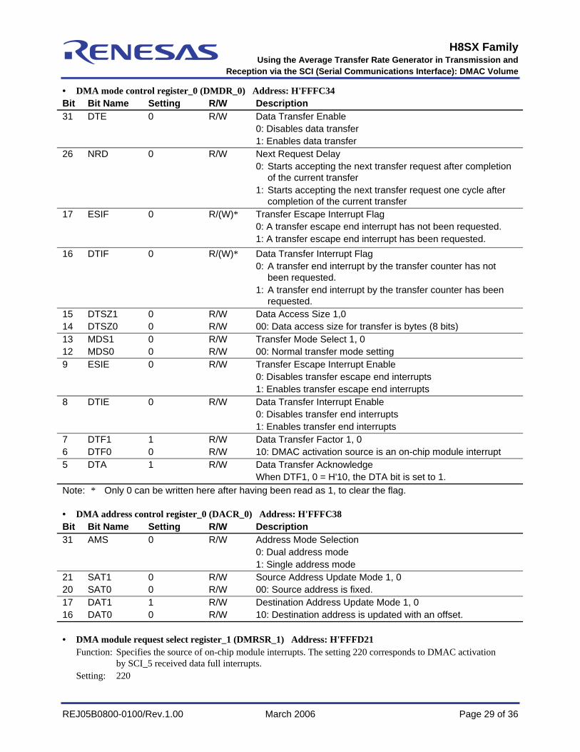
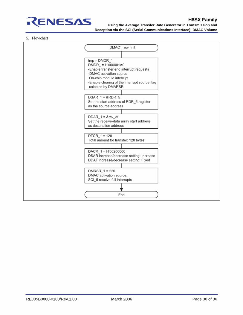
5.6.4 DMAC1_rcv_init Function 1. Overview
DMAC_1 initialization. Sets up the registers of DMAC channel for the transfer of received data from SCI_5. 2. Arguments
None 3. Return value
None 4. Description of internal register usage
Usage of internal registers in this task is described below. The given settings are those used in the task and differ from the initial settings.
• DMA source address register_1 (DSAR_1) Address: H'FFFC20
Function: Specifies the source address for the transfer. Setting: &RDR_5
• DMA destination address register_1 (DDAR_1) Address: H'FFFC24
Function: Specifies the destination address for the transfer. Setting: &rcv_dt
• DMA transfer count register_1 (DTCR_1) Address: H'FFFC2C
Function: Selects the amount of data to be transferred as 128 bytes. Setting: 128
H8SX Family
Using the Average Transfer Rate Generator in Transmission and Reception via the SCI (Serial Communications Interface): DMAC Volume
REJ05B0800-0100/Rev.1.00 March 2006 Page 29 of 36
• DMA mode control register_0 (DMDR_0) Address: H'FFFC34 Bit Bit Name Setting R/W Description 31 DTE 0 R/W Data Transfer Enable
0: Disables data transfer 1: Enables data transfer
26 NRD 0 R/W Next Request Delay 0: Starts accepting the next transfer request after completion of the current transfer 1: Starts accepting the next transfer request one cycle after completion of the current transfer
17 ESIF 0 R/(W)* Transfer Escape Interrupt Flag 0: A transfer escape end interrupt has not been requested. 1: A transfer escape end interrupt has been requested.
16 DTIF 0 R/(W)* Data Transfer Interrupt Flag 0: A transfer end interrupt by the transfer counter has not been requested. 1: A transfer end interrupt by the transfer counter has been requested.
15 14
DTSZ1 DTSZ0
0 0
R/W R/W
Data Access Size 1,0 00: Data access size for transfer is bytes (8 bits)
13 12
MDS1 MDS0
0 0
R/W R/W
Transfer Mode Select 1, 0 00: Normal transfer mode setting
9 ESIE 0 R/W Transfer Escape Interrupt Enable 0: Disables transfer escape end interrupts 1: Enables transfer escape end interrupts
8 DTIE 0 R/W Data Transfer Interrupt Enable 0: Disables transfer end interrupts 1: Enables transfer end interrupts
7 6
DTF1 DTF0
1 0
R/W R/W
Data Transfer Factor 1, 0 10: DMAC activation source is an on-chip module interrupt
5 DTA 1 R/W Data Transfer Acknowledge When DTF1, 0 = H'10, the DTA bit is set to 1.
Note: * Only 0 can be written here after having been read as 1, to clear the flag. • DMA address control register_0 (DACR_0) Address: H'FFFC38 Bit Bit Name Setting R/W Description 31 AMS 0 R/W Address Mode Selection
0: Dual address mode 1: Single address mode
21 20
SAT1 SAT0
0 0
R/W R/W
Source Address Update Mode 1, 0 00: Source address is fixed.
17 16
DAT1 DAT0
1 0
R/W R/W
Destination Address Update Mode 1, 0 10: Destination address is updated with an offset.
• DMA module request select register_1 (DMRSR_1) Address: H'FFFD21
Function: Specifies the source of on-chip module interrupts. The setting 220 corresponds to DMAC activation by SCI_5 received data full interrupts. Setting: 220
H8SX Family
Using the Average Transfer Rate Generator in Transmission and Reception via the SCI (Serial Communications Interface): DMAC Volume
REJ05B0800-0100/Rev.1.00 March 2006 Page 30 of 36
5. Flowchart
End
DMAC1_rcv_init
tmp = DMDR_1
DMDR_ = H'000001A0
-Enable transfer end interrupt requests
-DMAC activation source:
On-chip module interrupt
-Enable clearing of the interrupt source flag
selected by DMARSR
DSAR_1 = &RDR_5
Set the start address of RDR_5 register
as the source address
DDAR_1 = &rcv_dt
Set the receive-data array start address
as destination address
DTCR_1 = 128
Total amount for transfer: 128 bytes
DACR_1 = H'00200000
DSAR increase/decrease setting: Increase
DDAT increase/decrease setting: Fixed
DMRSR_1 = 220
DMAC activation source:
SCI_5 receive full interrupts
H8SX Family
Using the Average Transfer Rate Generator in Transmission and Reception via the SCI (Serial Communications Interface): DMAC Volume
REJ05B0800-0100/Rev.1.00 March 2006 Page 31 of 36
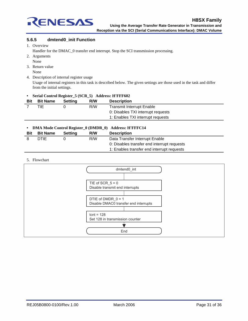
5.6.5 dmtend0_init Function 1. Overview
Handler for the DMAC_0 transfer end interrupt. Stop the SCI transmission processing. 2. Arguments
None 3. Return value
None 4. Description of internal register usage
Usage of internal registers in this task is described below. The given settings are those used in the task and differ from the initial settings.
• Serial Control Register_5 (SCR_5) Address: H'FFF602 Bit Bit Name Setting R/W Description 7 TIE 0 R/W Transmit Interrupt Enable
0: Disables TXI interrupt requests 1: Enables TXI interrupt requests
• DMA Mode Control Register_0 (DMDR_0) Address: H'FFFC14 Bit Bit Name Setting R/W Description 8 DTIE 0 R/W Data Transfer Interrupt Enable
0: Disables transfer end interrupt requests 1: Enables transfer end interrupt requests
5. Flowchart
End
dmtend0_int
TIE of SCR_5 = 0
Disable transmit end interrupts
DTIE of DMDR_0 = 1
Disable DMAC0 transfer end interrupts
tcnt = 128
Set 128 in transmission counter
H8SX Family
Using the Average Transfer Rate Generator in Transmission and Reception via the SCI (Serial Communications Interface): DMAC Volume
REJ05B0800-0100/Rev.1.00 March 2006 Page 32 of 36
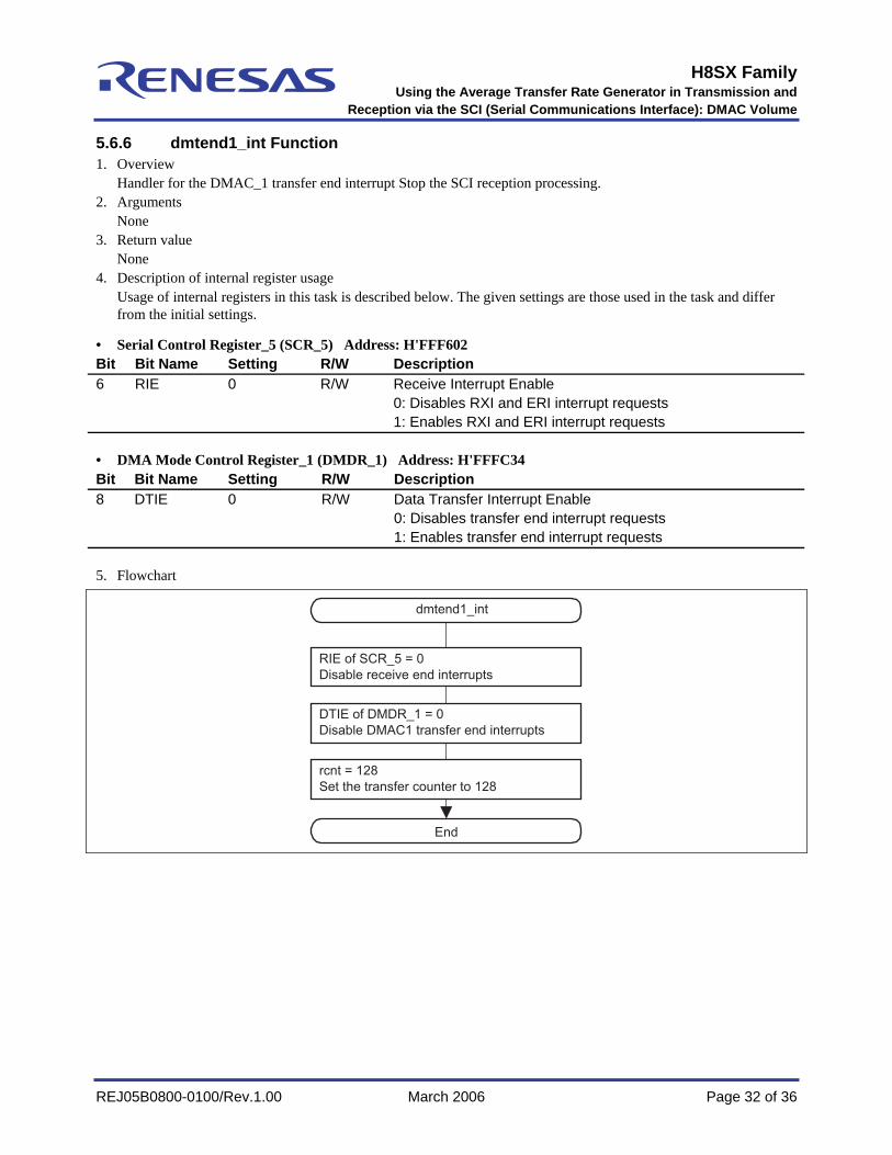
5.6.6 dmtend1_int Function 1. Overview
Handler for the DMAC_1 transfer end interrupt Stop the SCI reception processing. 2. Arguments
None 3. Return value
None 4. Description of internal register usage
Usage of internal registers in this task is described below. The given settings are those used in the task and differ from the initial settings.
• Serial Control Register_5 (SCR_5) Address: H'FFF602 Bit Bit Name Setting R/W Description 6 RIE 0 R/W Receive Interrupt Enable
0: Disables RXI and ERI interrupt requests 1: Enables RXI and ERI interrupt requests
• DMA Mode Control Register_1 (DMDR_1) Address: H'FFFC34 Bit Bit Name Setting R/W Description 8 DTIE 0 R/W Data Transfer Interrupt Enable
0: Disables transfer end interrupt requests 1: Enables transfer end interrupt requests
5. Flowchart
End
dmtend1_int
RIE of SCR_5 = 0
Disable receive end interrupts
DTIE of DMDR_1 = 0
Disable DMAC1 transfer end interrupts
rcnt = 128
Set the transfer counter to 128
H8SX Family
Using the Average Transfer Rate Generator in Transmission and Reception via the SCI (Serial Communications Interface): DMAC Volume
REJ05B0800-0100/Rev.1.00 March 2006 Page 33 of 36
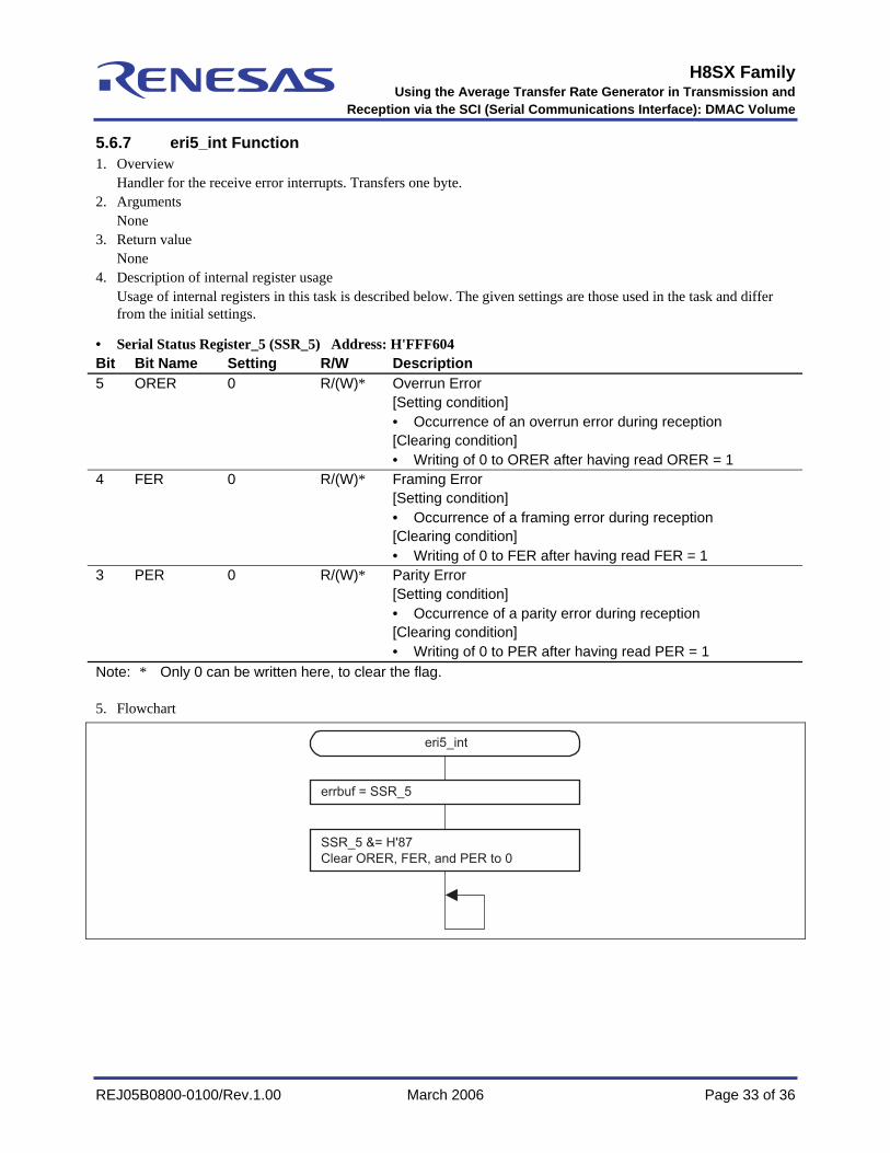
5.6.7 eri5_int Function 1. Overview
Handler for the receive error interrupts. Transfers one byte. 2. Arguments
None 3. Return value
None 4. Description of internal register usage
Usage of internal registers in this task is described below. The given settings are those used in the task and differ from the initial settings.
• Serial Status Register_5 (SSR_5) Address: H'FFF604 Bit Bit Name Setting R/W Description 5 ORER 0 R/(W)* Overrun Error
[Setting condition] • Occurrence of an overrun error during reception [Clearing condition] • Writing of 0 to ORER after having read ORER = 1
4 FER 0 R/(W)* Framing Error [Setting condition] • Occurrence of a framing error during reception [Clearing condition] • Writing of 0 to FER after having read FER = 1
3 PER 0 R/(W)* Parity Error [Setting condition] • Occurrence of a parity error during reception [Clearing condition] • Writing of 0 to PER after having read PER = 1
Note: * Only 0 can be written here, to clear the flag. 5. Flowchart
eri5_int
errbuf = SSR_5
SSR_5 &= H'87
Clear ORER, FER, and PER to 0
H8SX Family
Using the Average Transfer Rate Generator in Transmission and Reception via the SCI (Serial Communications Interface): DMAC Volume
REJ05B0800-0100/Rev.1.00 March 2006 Page 34 of 36
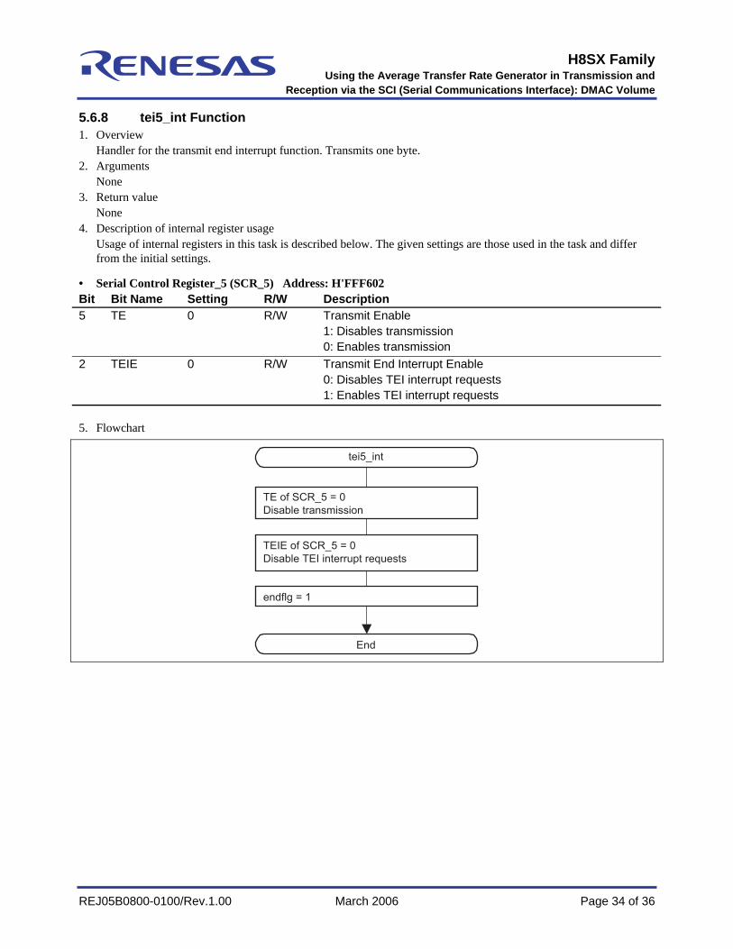
5.6.8 tei5_int Function 1. Overview
Handler for the transmit end interrupt function. Transmits one byte. 2. Arguments
None 3. Return value
None 4. Description of internal register usage
Usage of internal registers in this task is described below. The given settings are those used in the task and differ from the initial settings.
• Serial Control Register_5 (SCR_5) Address: H'FFF602 Bit Bit Name Setting R/W Description 5 TE 0 R/W Transmit Enable
1: Disables transmission 0: Enables transmission
2 TEIE 0 R/W Transmit End Interrupt Enable 0: Disables TEI interrupt requests 1: Enables TEI interrupt requests
5. Flowchart
End
tei5_int
TE of SCR_5 = 0
Disable transmission
TEIE of SCR_5 = 0
Disable TEI interrupt requests
endflg = 1
H8SX Family
Using the Average Transfer Rate Generator in Transmission and Reception via the SCI (Serial Communications Interface): DMAC Volume
REJ05B0800-0100/Rev.1.00 March 2006 Page 35 of 36
Revision Record Description
Rev. Date Page Summary
1.00 Mar.10.06 — First edition issued
H8SX Family
Using the Average Transfer Rate Generator in Transmission and Reception via the SCI (Serial Communications Interface): DMAC Volume
REJ05B0800-0100/Rev.1.00 March 2006 Page 36 of 36
1. These materials are intended as a reference to assist our customers in the selection of the Renesas
Technology Corp. product best suited to the customer's application; they do not convey any license
under any intellectual property rights, or any other rights, belonging to Renesas Technology Corp. or
a third party.
2. Renesas Technology Corp. assumes no responsibility for any damage, or infringement of any third-
party's rights, originating in the use of any product data, diagrams, charts, programs, algorithms, or
circuit application examples contained in these materials.
3. All information contained in these materials, including product data, diagrams, charts, programs and
algorithms represents information on products at the time of publication of these materials, and are
subject to change by Renesas Technology Corp. without notice due to product improvements or
other reasons. It is therefore recommended that customers contact Renesas Technology Corp. or
an authorized Renesas Technology Corp. product distributor for the latest product information
before purchasing a product listed herein.
The information described here may contain technical inaccuracies or typographical errors.
Renesas Technology Corp. assumes no responsibility for any damage, liability, or other loss rising
from these inaccuracies or errors.
Please also pay attention to information published by Renesas Technology Corp. by various means,
including the Renesas Technology Corp. Semiconductor home page (http://www.renesas.com).
4. When using any or all of the information contained in these materials, including product data,
diagrams, charts, programs, and algorithms, please be sure to evaluate all information as a total
system before making a final decision on the applicability of the information and products. Renesas
Technology Corp. assumes no responsibility for any damage, liability or other loss resulting from the
information contained herein.
5. Renesas Technology Corp. semiconductors are not designed or manufactured for use in a device or
system that is used under circumstances in which human life is potentially at stake. Please contact
Renesas Technology Corp. or an authorized Renesas Technology Corp. product distributor when
considering the use of a product contained herein for any specific purposes, such as apparatus or
systems for transportation, vehicular, medical, aerospace, nuclear, or undersea repeater use.
6. The prior written approval of Renesas Technology Corp. is necessary to reprint or reproduce in
whole or in part these materials.
7. If these products or technologies are subject to the Japanese export control restrictions, they must
be exported under a license from the Japanese government and cannot be imported into a country
other than the approved destination.
Any diversion or reexport contrary to the export control laws and regulations of Japan and/or the
country of destination is prohibited.
8. Please contact Renesas Technology Corp. for further details on these materials or the products
contained therein.
1. Renesas Technology Corp. puts the maximum effort into making semiconductor products better and
more reliable, but there is always the possibility that trouble may occur with them. Trouble with
semiconductors may lead to personal injury, fire or property damage.
Remember to give due consideration to safety when making your circuit designs, with appropriate
measures such as (i) placement of substitutive, auxiliary circuits, (ii) use of nonflammable material or
(iii) prevention against any malfunction or mishap.
Keep safety first in your circuit designs!
Notes regarding these materials