Embed Size (px)
Citation preview
UNIVERSITY OF CALIFORNIA
Lawrence Radiation Laboratory Berkeley, California
AEC Contract No. W-7405-eng-48
UCRL-3307 (Rev. 3)
LAWRENCE RADIATION LABORATORY COUNTING HANDBOOK
Edited by
Nuclear Instrumentation Groups
October 1, 1966

UCRL-3307 (Rev. 3)
PREFACE
The Counting Handbook is a compilation of operational techniques and performance specifications on counting equipment in use at the Lawrence Radiation Laboratory, Berkeley. Counting notes have been written from the viewpoint of the user rather than that of the designer or maintenance man. The only maintenance instructions that have been included are those that can easily be performed by the experimenter to assure himself that the equipment is operating properly.
Suggestions for additional notes to be included in :fUture revisions of the Handbook are most welcome.
Mary Lou Rentler and Mary Thibideau were responsible for the final typing of the counting notes; we greatly appreciate their patience and fine work.
October 1, 1966
Lawrence Radiation Laboratory, University of California, Berkeley
COUNTING HANDBOOK
CHECK LIST
NOTE: Circle the Counting Note number which is missing, fill in your name at the bottom of Page 2, and return to Dick A. Mack.
------·-FILE NUMBER
Contents
cc 1-2A Pages 1 -
cc 1-4 Pages 1 -
--·------cc 1-6
Pages 1 -
cc 1-7 Pages 1 -
cc 1-8 Pages 1 -
CC 2-lB Pages 1 -
CC 2-2C Pages 1 -
CC 2-6B Pages 1 -
CC 3-5B Pages 1 -
. -DATE
-· ... 0
-----12-15-63
2. ...
1-10-56 10
1-14-64 2.
...
2-6-64 8.
2-15-66 1.
7-26-66 13. ...
5-31-66 19. --·-
5-28-64 15.
3-11-64 2.
----CC 3-lOA
Pages 1 -
cc 3-11 Pages 1 -
12-15-63 8.
----······· 11-21-60
7.
·-FILE NUMBER DATE
--cc 3-12 1-10-64
Pages 1 - 2.
cc 3-13 1-13-64 Pages 1 - 2.
cc 3-14 1-10-64 Pages 1 - 2.
cc 3-15 3-11-64 Pages 1 - 11.
cc 3-16 2-15-66 Pages 1 - 2.
cc 4-6 6-8-64 Pages 1 - 4.
-cc 5-6 4-10-56
Pages 1 - 5. -
cc 5-7 4-10-56 Pages 1 - 2.
CC 5-8A 11-5-63 Pages 1 - 11.
CC 5-9A 9-3-66 Page 1.
CC 6-5A 6-30-66 Pages 1 - 10.
--
Check List (Continued) -2- October 1, 1966
FILE NUMBER DATE
cc 6-6 6-10-64 Pages 1 - 12.
cc 6-7 2-10-64 Pages 1 - 5.
-cc 6-8 8-10-64
Pages 1 - 4. -
CC 8-2C 12-21-64 Pages 1 - 13.
CC 8-3B 7-21-66 Pages 1 - 5.
CC 8-4A 3-5-64 Pages 1 - 14.
CC 8-5A 6-30-66 Pages 1 - 11.
cc 8-20 12-29-58 Pages 1 - 8.
cc 8-30 1-21-59 Pages 1 - 11.
cc 8-31 3-16-61 Pages 1 - 11. --
CC 9-5C 8-2-66 Pages 1 - 2.
CC 9-8A 2-15-66 Pages 1 - 8.
cc 9-9 1-13-64 Pages 1 - 2.
-·
Circle any missing notes and return list to:
Mr. Dick A. Mack University of California Lawrence Radiation Laboratory Berkeley, California, U.S.A. 94720
Name
FILE NUMBER
cc 9-10 Pages 1 - 8.
cc 9-11 Pages 1 - 3.
cc 10-1 Pages 1 - 6.
cc 10-3 Pages 1 - 9.
cc 10-4 Pages 1 - 8.
cc 10-5 Pages 1 - 6.
cc io-6 Pages 1 - 3.
cc 10-7 Pages 1 - 4.
cc 10-8 Pages 1 - 4.
cc 10-9 Pages 1 - 3.
cc 10-lOA Pages 1 - 8.
cc 10-11 Pages 1 - 3.
cc 10-12 Pages 1 - 3.
cc 10-13 Pages 1 - 3.
Index
~~~~~--~~~~~~~~~~
Address ~~~~~~~~~~~~~~~~
DATE
4-2-64
2-15-66
1-10-59
12-24-58
3-15-61
6-20-62
1-13-64
1-14-64
1-13-64
1-14-64
6-30-66
2-15-66
3-15-66
8-3-66
TABLE OF CONTENTS
AMPLIFIERS
Summary of Nanosecond Pulse Amplifiers Evaluation of HP-460A and B Amplifiers Logic Amplifier 20 V Output Pulse Amnlifier Dual lNs - DCxlO Amplifier
CABLES AND COAXIAL COMPONENTS
Pulse Response of Coaxial Cables Physical Characteristics of Coaxial Cables Nanosecond - Pulse Transformers, Attenuators
and Terminators
COINCIDENCE SYSTEMS AND DISCRIMINATORS
Radiation Laboratory Amplitude Discriminators Dual 3-Channel Positive Input Coincidence and
Anti-Coincidence Unit, Model 3 Pulse-Amplitude Discriminator Model 2 and 3 4-Way "AND", 1 "INHIBIT" Circuit 5-Way "OR" Circuit 5-Way Fanout Time-to-Height Conversion System 5-Way Fanout
COMPONENTS FOR AMPLITUDE ANALYSIS . .
Summary of Pulse Height Analyzer Manufacturer's Data
DEFINITIONS AND STANDARDS ----Definition of Performance Measurement Definition of Pulse Terms Definitions of Terms Related to Phototubes Logical Voltage Levels
ELECTRONIC CIRCUITS FOR SPARK CHAMBERS
Spark Gap Trigger Amplifier Spark Chamber Energy Distribution Box A High Voltage Probe for Nanosecond Pulses 15 Kv 20 ma Spark Chamber Booster Supply
OSCILLOSCOPES & MONITORING
October 1, 1966
Section
cc 1
CC l-2A cc 1-4 cc 1-6 cc 1-7 cc 1-8
cc 2
CC 2-lB CC 2-2C CC 2-6B
cc 3
cc 3-5B cc 3-lOA
cc 3-11 cc 3-12 cc 3-13 cc 3-14 cc 3-15 cc 3-16
cc 4
cc 4-6
cc 5
cc 5-6 cc 5-7 cc 5-8A cc 5-9A
cc 6
cc 6-5A cc 6-6 cc 6-7 cc 6-8
cc 7
Table of Contents (Continued) -2-
PHOTOMULTIPLIERS AND SCINTILLATORS
Multiplier Phototube, Manufacturers' Data Phototube Measuring Techniques 6810 Class Photomultiplier Special Character-
istics Particle Detection by Scintillation Counters Electrical Gating of Multiplier Phototubes A Generator of Fast Light Pulses for
Photomultiplier Tube Testing Corona Light Pulsers
SCALER~ AND READOUT EQUIPMENT
Radiation Laboratory Scalers Operating Characteristics
Decade Scaler, Model 5 Register Unit A Decade Scaler and Readout System 10 MHz Decade Scaler
WAVEFORM GENERATORS AND POWER SUPPLIES
Mercury Pulsers Nanosecond Pulse Generator Gated Pulse Generator Del-a-gate Delay Gate Relay Driver Pulse Generators Pulse Generator High-Voltage Power for Multiplier Phototubes Dual Delay Gate Pulse Generator Nuclear Instrument Module Bin
October 1, 1966
cc 8
CC 8-2C CC 8-3B CC 8-4A
CC 8-5A cc 8-20 cc 8-30
cc 8-31
cc 9
CC 9-5C
CC 9-8A cc 9-9 cc 9-10 cc 9-11
cc 10
cc 10-1 cc 10-3 cc 10-4 cc 10-5 cc 10-6 cc 10-7 cc 10-8 cc 10-9 CC 10-lOA cc 10-11 cc 10-12 cc 10-13

File No. CC l-2A (1) December 15, 1963 D. A. Mack
Lawrence Radiation Laboratory, University of California, Berkeley
COUNTING NOTE
SUMMARY OF NANOSECOND PULSE AMPLIFIERS
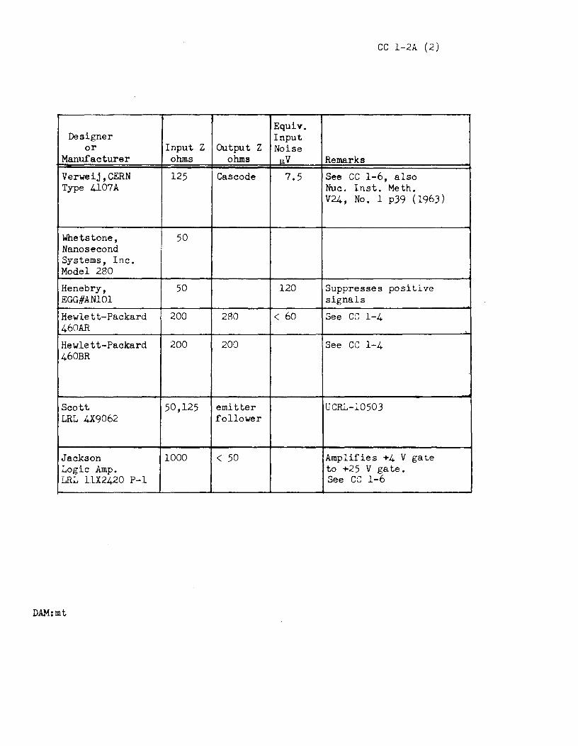
I. SUMMARY Listed below are several amplifiers which are useful primarily for
preserving timing information in nuclear instrumentation.
Designer Rise Fall Max. or Time Time Output Delay
Manufacturer Gain nsec nsec Signal nsec
Verweij,CERN 10 2.2 + sig. ±6 v 6. 5 +in +out Type 4107A xo. 5,xo. 25 ,xo.1 2.5 - sig. into 7.5 +in -out
step atten. 125 Q 7.5 -in +out invert & non- 8.5 -in -out invert
Whetstone, 10 2 ±1.5 v Nanosecond non-invert into 50Q Systems, Inc. Model 280 Henebry, 4.0 ± 10% 2.2 2.5 0.4 v 2.5 EGG#ANlOl non-invert into 50Q Hewlett-Packard 10 ±4 V into 18 460AR non-invert 200 Q Hewlett-Packard 5. 6 "Linear "Opr. 2.6 2.6 ±8 v 21 460BR 16 'Pulse 11 Opr. 2.6 2.6 into 200Q
inverting -125 v into open circuit
Scott 3-10 for 50Q 3 3 ±1.5 v LRL 4X9062 input into 50Q
1. 2-4 for 125 Q input
Jackson 5 45 < 15 Logic Amp. non-invert LRL 11X2420P-l
I
--
I
CC l-2A (2)
Equiv. Designer Input
or Input z Output Z Noise Manufacturer ohms ohms uV Remarks Verweij,CERN 125 Cascode 7.5 See CC 1-6, also Type 4107A Nuc. Inst. Meth.
V24, No. 1 p39 (1963)
Whetstone, 50 Nanosecond Systems, Inc. Model 280 Henebry, 50 120 Suppresses positive EGG#ANlOl signals Hewlett-Packard 200 280 < 60 See cc 1-4 460AR Hewlett-Packard 200 200 See cc 1-4 460BR
Scott 50,125 emitter UCRL-10503 LRL 4X9062 follower
Jackson 1000 < 50 Amplifies +4 V gate Logic Amp. to +25 V gate. LRL llX2420 P-1 See CC 1-6
DAM: mt

Radiation Laboratory, University of California, Berkeley.
COUNTING NOI'E
DISTRIBUTED AMPLIFIERS
File No• CC 1-4 Page 1 .ran. 10, 1956 Frank Evans
ABSTRACT: Distributed amplifiers may be used to amplify pulses having rise times less than lO_g sec. The output pulses will be produced with negligible overshoots if the frequency response at the high end closely approxinntes a Gaussian charac-teristic. Saturation and cutoff characteristics of most distributed amplifiers nermit their use as limiters• The Hewlett-Packard 460A and 460B, having individ-ual rise times of 2.6 x lo-9 sec., are good examples of these amplifiers.
TEXT: By the cascading of individual stages, amplifiers can be designed to give appreciable gain over bandwidths of the order of tens of megacycles• The limita-tion here is the ratio of transconductance to the sum of input and output capaci-tances available in vacuum tubes at present. The distributed amplifier design, (1), (2), furnishes means of isolating the effects of individual tube capacitances, and, at the same time, of taking advantage of the transconductance in an additive manner for many tubes in parallel• The input circuit consists of grids tapped in spacially along an artificial, or lumped, transmission line of which the tube input capacitances form a part. Similarly the plates are tapped into a second trans-mission line. An input pulse will travel down the first line, and cause each tube to conduct in sequence. Current pulses from the plates will travel in both direc-tions in the second line. In one direction these pulses add together and travel toward the output or load. The pulses traveling in the reverse direction are absorbed by an internal resistive termination. In this manner sizeable gains may be achieved over bandwidths of hundreds of megacycles.
The Hewlett-Packard 460A and 460B distributed amplifiers are designed primarily as pulse amplifiers but under some restrictions they may be used for cw. In general the 460B is intended for higher signal levels than the 460A. Both units have rise times of 2.6 x lo-9 sac., although the 460A has more gain into a matched load. Fre-quently the 460A is used to amplify pulses directly from the anode of a photomulti-plier, while the 460B, because of its greater output capabilities, might be used to drive directly the vertical deflection plates of a high speed cathode ray tube·
The front panel of the 460A is shown below in Fig• l•
Fig. 1 Hewlett Packard 460A - Front view•
Aside from the ON-OFF power switch, the only control accessible is the GAIN. This control determines the grid bias, and consequently the transconductance, of the five 6AK5 (or 5654, in late models) tubes comprising the first stage• Since the 460A is a two stage distributed amplifier (the second stage consists of 7 tubes) there is no inversion of an input pulse. The input and output connectors shown are to be used with 200 ohm Transradio C3-T cable assemblies• If it should be desired
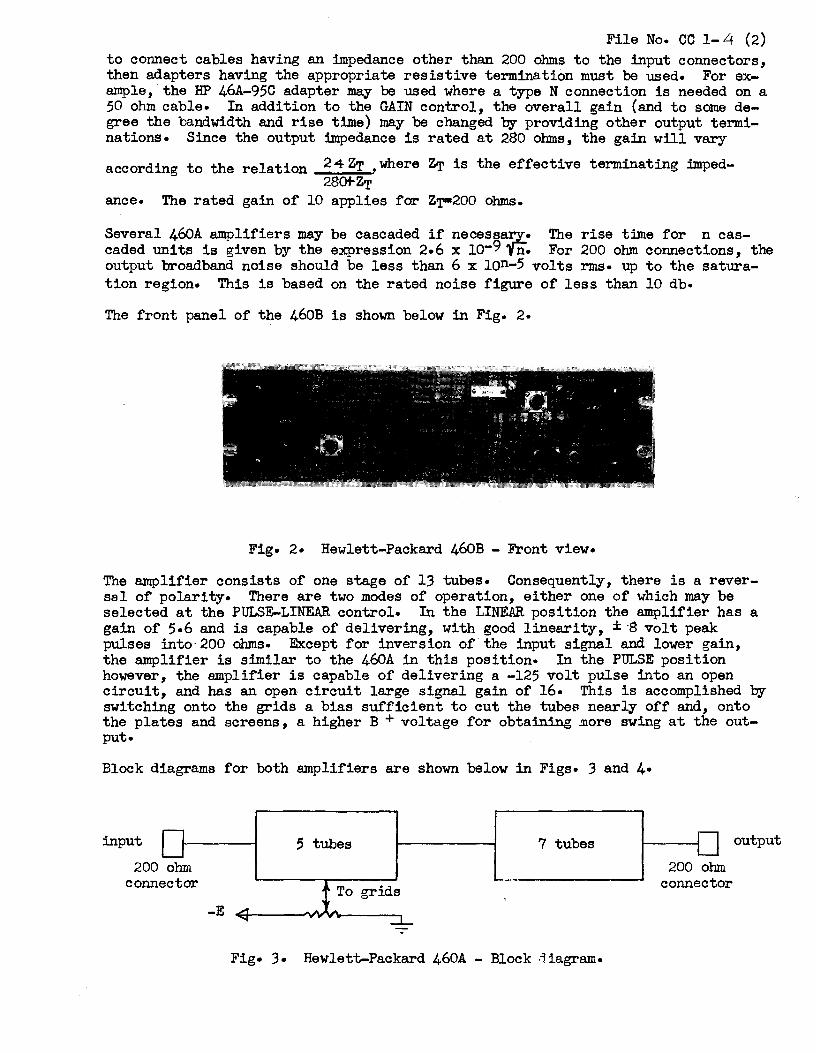
File No. CC 1- 4 (2) to connect cables having an impedance other than 200 ohms to the input connectors, then adapters having the appropriate resistive termination must be used. For ex-ample, the HP 46A-95C adapter may be used where a type N connection is needed on a 50 ohm cable. In addition to the GAIN control, the overall gain (and to some de-gree the bandwidth and rise time) may be changed by providing other output termi-nations. Since the output impedance is rated at 280 ohms, the gain will vary
according to the relation 24 ZT where ZT is the effective terminating imped-2SOf-ZT
ance. The rated gain of 10 applies for. ZT•200 ohms.
Several 460A amplifiers may be cascaded if necessru:.:z.• The rise time for n cas-caded units is given by the expression 2.6 x lo-9vn. For 200 ohm connections, the output broadband noise should be less than 6 x lon-5 volts rms• up to the satura-tion region. This is based on the rated noise figure of less than 10 db·
The front panel of the 460B is shown below in Fig. 2·
Fig• 2• Hewlett-Packard 460B - Front view.
The amplifier consists of one stage of 13 tubes. Consequently, there is a rever-sal of polarity• There are two modes of operation, either one of which may be selected at the PULSF.-LINEAR control. In the LINEAR position the amplifier has a gain of 5.6 and is capable of delivering, with good linearity, ± ·B volt peak pulses into·200 ohms. Except for inversion of the input signal and lower gain, the amplifier is similar to the 460A in this position• In the PULSE position however, the amplifier is capable of delivering a -125 volt pulse into an open circuit, and has an open circuit large signal gain of 16. This is accomplished by switching onto the grids a bias sufficient to cut the tubes nearly off and, onto the plates and screens, a higher B +voltage for obtaining ~ore swing at the out-put.
Block diagrams for both amplifiers are shown below in Figs• 3 and 4•
input
200 ohm connector.
-E
5 tubes 7 tubes
grids
Fig• 3· Hewlett-Packard 460A - Block diagram•
200 ohm connector
output
input
200 ohm connector
13 tubes
To grids
"Pulse"
t -1·9v· -10v. llOv.
To plates and screens
'l.
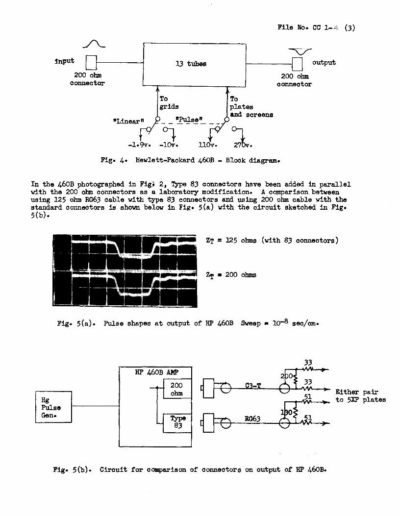
File No. CC 1-4 (3)
200 ohm connector
output
Fig. 4• Hewlett-Packard 46oB - Block diagram.
In the 460B photographed in Fig• 2, Type 83 connectors have been added in parallel with the 200 ohm connectors as a laboratory modification. A comparison between using 125 ohm RG63 cable with type 83 connectors and using 200 ohm cable with the standard connectors is shown below in Fig• 5(a) with the circuit sketched in Fig• 5(b).
ZT = 125 ohms (with 83 connectors)
ZT • 200 ohms
Fig• 5(a)• Pulse shapes at output or HP 460B Sweep • 10-8 sec/cm•
33 HP 460B AMP
- - 200 ohm
Hg Pulse Gen. Type RG63 - 83
Fig• 5(b)• Circuit £or comparison or connectors on output or HP 460B.
Either pair to 5XP plates
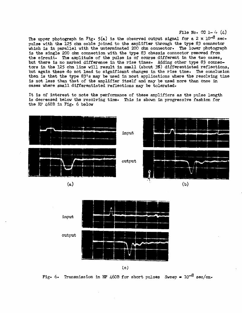
File No. CC 1-4 (4) The upper photograph in Fig· 5(a) is the observed output signal for a 2 x 10⁻⁸ sec• pulse with the 125 ohm cable joined to the amplifier through the type 8.3 connector which is in parallel with the unterminated 200 ohm connector• The lower photograph is the single 200 ohm connection with the type 8.3 chassis connector removed .from the circuit. The amplitude of the p'lilse is of course different in the two cases, but there is no marked difference in the rise times. Adding other type 83 connec-tors in the 125 ohm line will result in small (about 3%) differentiated reflections, but again these do not lead to significant changes in the rise time. The conclusion then is that the type 8J 1s may be used in most applications where the resolving time is not less than that of the amplifier itself and may be used more than once in cases where small differentiated reflections may be tolerated.
It is of interest to note the performance of these amplifiers as the pulse length is decreased below the resolving time• This is shown in progressive fashion for the HP 460B in Fig. 6 below
input
output
(a) (b)
input
output
(c)
Fig• 6. Transmission in HP 460B for short pulses Sweep • 10-8 sec/cm•
File No. CC 1-4 (5)
The input pulse, shown in the upper half of ~ach photograph, was adjusted in amplitude for an output of approximately 1 cmo Fig. 6(2) shows a flat top pulse for both input and output, indicating the rated pulse gain and rise time• In 6(b) the pulse has been narrowed down to about the rise time of the amplifier, and more amplitude is required for the same output• In addition, products due to phase distortion are beginning to appearo In 6(c) the pulse has been fUrther narrowed so that there is about unity gain on the peak amplitude and a consider-able increase in the relative amplitudes of the distortion products.
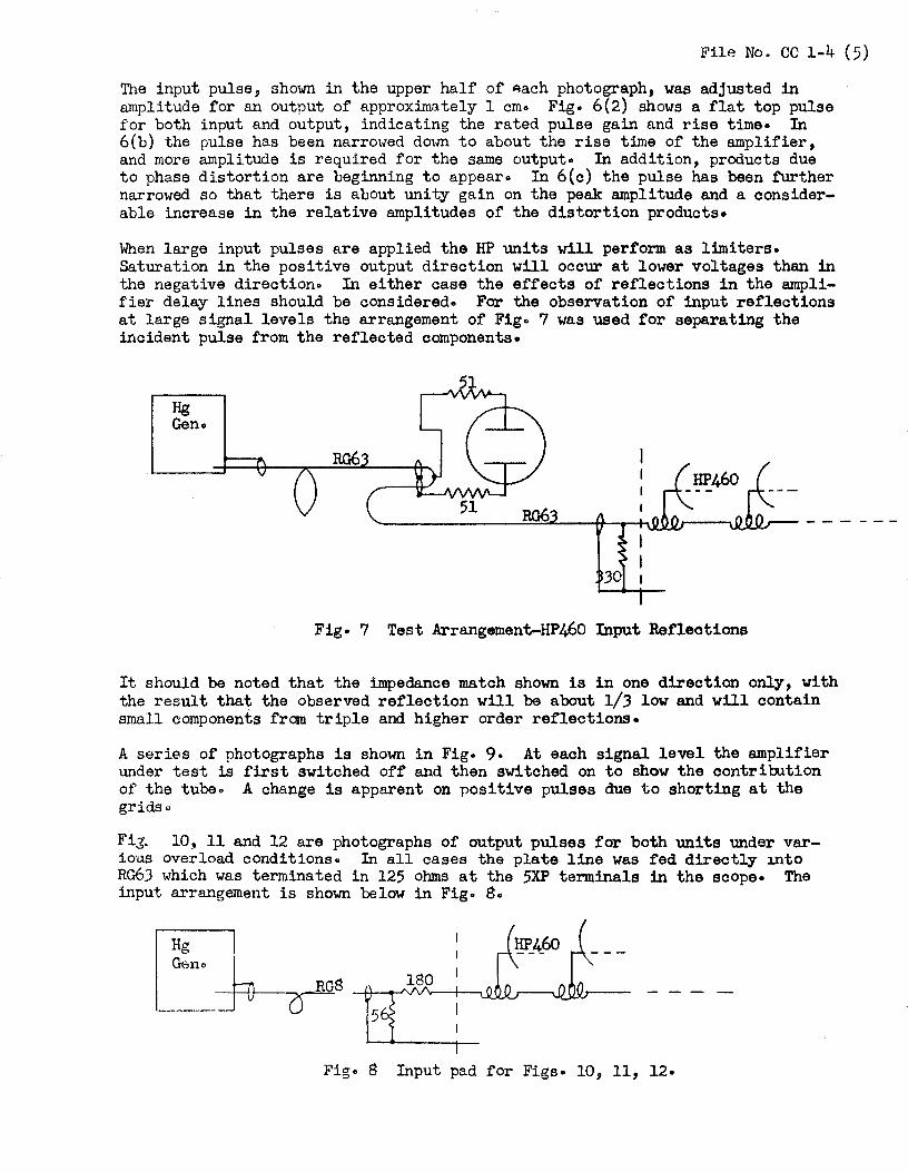
When large input pulses are applied the HP units will perform as limiters. Saturation in the positive output direction will occur at lower voltages than in the negative directiono In either case the effects of reflections in the ampli-fier delay lines should be considered. For the observation of input reflections at large signal levels the arrangement of Fig. 7 was used for separating the incident pulse from the reflected components•
Hg Geno
30 I
Fig• 7 Test Arrangement-HP460 Input Reflections
It should be noted that the impedance match shown is in one direction only, with the result that the observed reflection will be about 1/3 low and will contain small components from triple and higher order reflections•
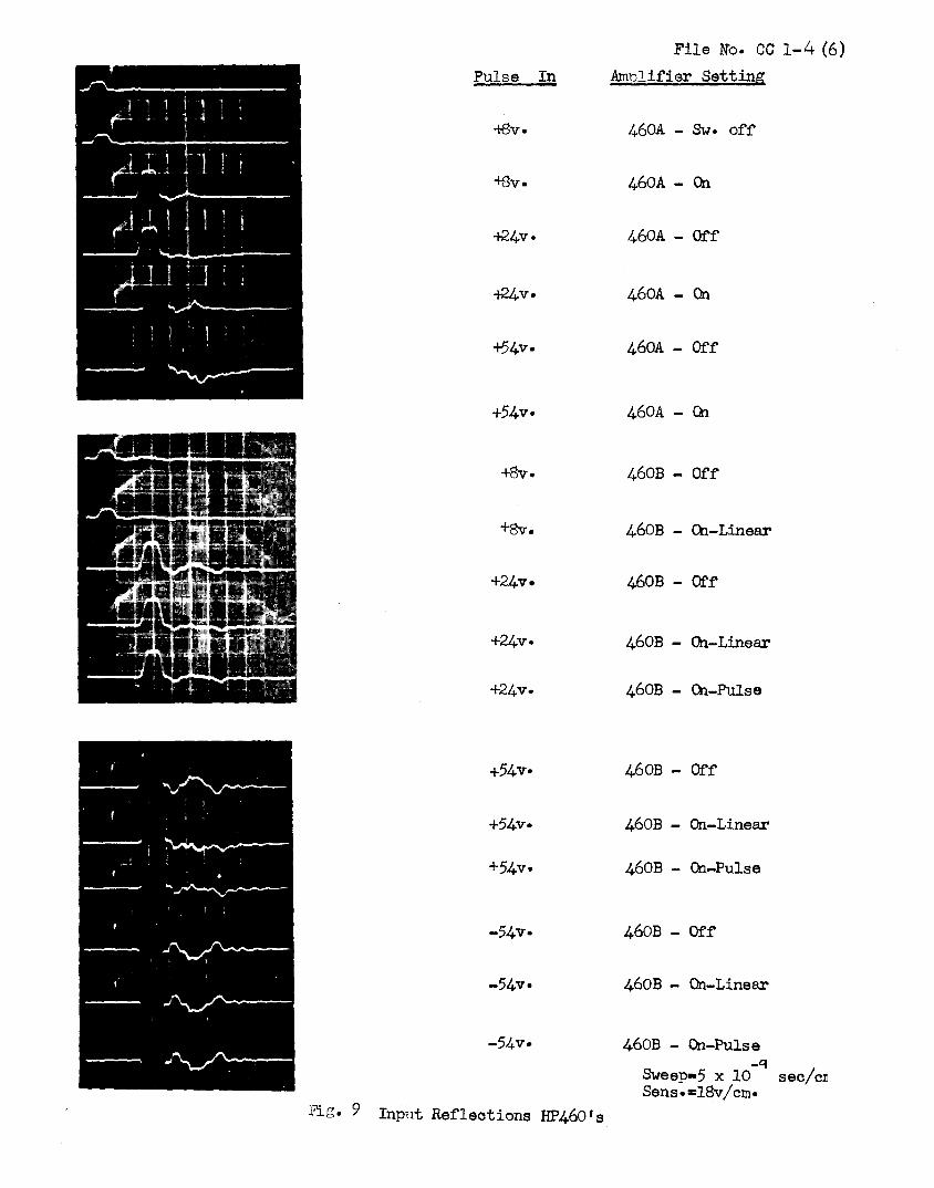
A series of photographs is shown in Fig· 9. At each signal level the amplifier under test is first switched off and then switched on to show the contribution of the tubeo A change is apparent on positive pulses due to shorting at the gridso
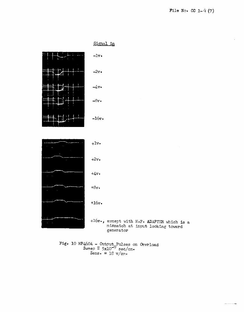
Fig. 10, 11 and 12 are photographs of output pulses for both units under var-ious overload conditions. In all cases the plate line was fed directly into RG6J which was terminated in 125 ohms at the 5XP terminals in the scope• The input arrangement is shown below in Fig. 80
5
Fige 8 Input pad for Figs• 10, 11, 12·
Pulse In
-t8v.
-t$v.
+24V•
-1-24v•
+?4v•
+54v•
+8v.
+8v.
+24v•
+24v•
+24v.
+54V•
+54v•
-54V•
-54V•
-54V•
Pig. 9 Input Reflections HP460•s
File No. CG 1-4 (6) Amolifier Setting
460A - Sw. off
460A - On
460A - Off
460A - On
460A - Off
460A - Ch
460B - Off
460B - On-Linear
460B - Off'
460B - On-Linear
460B - On-Pulse
460B - Off
460B - On-Linear
460B - Ch-Pulse
460B - Off'
460B - On-Linear
460B - On-Pulse -ct
Sweep•5 x 10 sec/cD Sens·=l8v/cm•
File No. CC 1-4 (7)
Signal in
-lv•
-2v·
-4V•
-8v.
-16v.
+lv.
+2v.
+4V•
+8v.
+16v.
+l6v., except with H.p. ADAPTER which is a mismatch at input looking toward generator
Fig. 10 HP460A - Output Pulses on Overload Sweep = 5xlo-9 sec/cm.
Sens. = 18 v/cm.
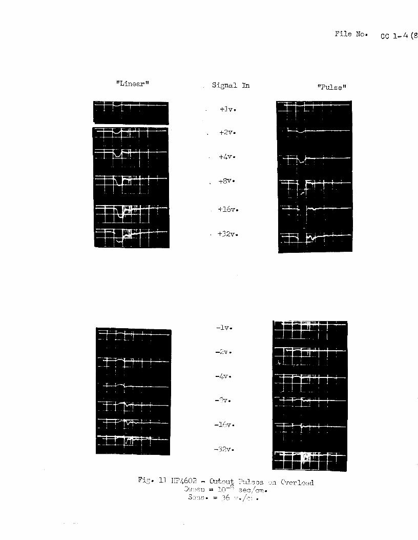
File No. cc 1-4 (8
"Line2-r 11 Signal In "Pulse"
+lv.
+2V•
+SV•
. +16v.
. +32v.
-lv.
-2V•
-16v.
-32V•
Fit;• 11 IIP!;.60B - Oub'!uX Fn1ses cm Overload = 10-c :Jee/err;.
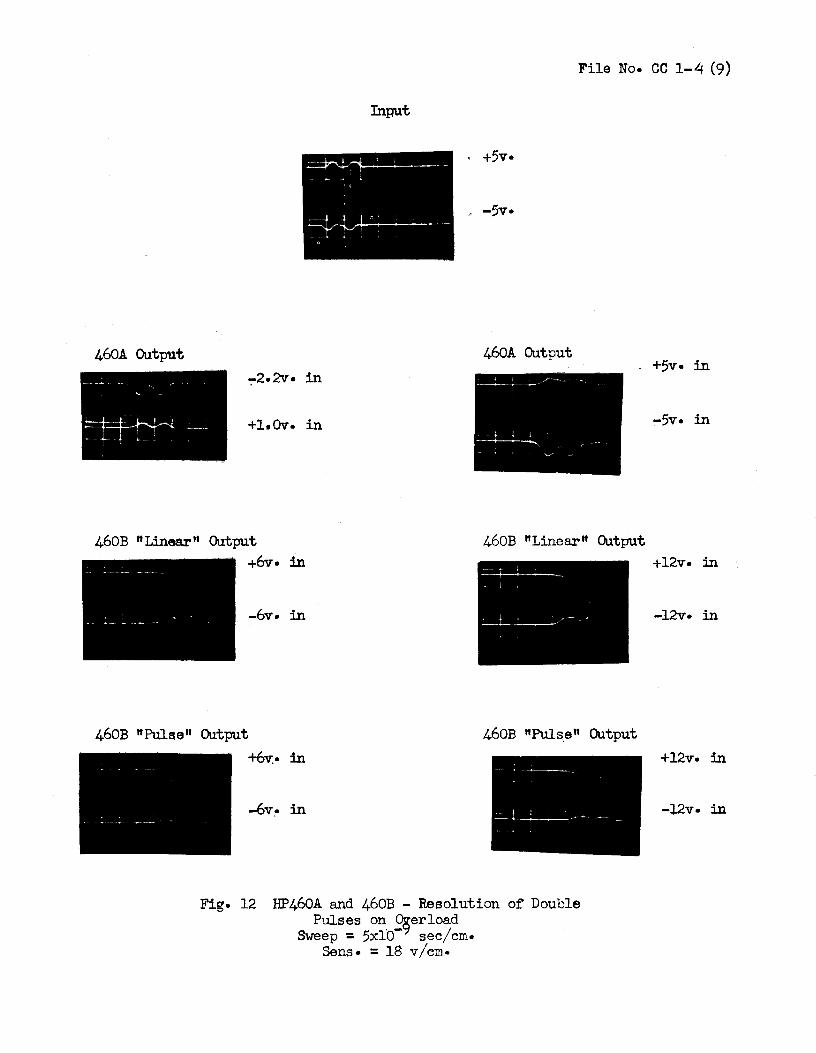
File No. CC 1-4 (9)
Input
· +5v•
460A Output 460A Output . +5v• in
+1.0v· in -5V• in
460B "Linear" Output 460B "Linear" Output +6v· in
-6v. in
460B "Pulae" Output 460B "Puls.a" Output +6v.• in
-6v.• in
Fig. 12 HP460A and 460B - Resolution of Double Pulses on ~erload
Sweep = 5xlb- sec/cm• Sens• = 18 v/cm•
+12V• in
-12v· in
+12v· in
-l2V• in
File No. CCl-l~ (10)
As shown in Figs. 10 and 11 there are peaks occurring after the pulse• In addi-tion, if there is an input mismatch the pulse may be lengthened due to reflections in the grid line. This is illustrated in the bottom trace of Fig. 10.
In Fig• 12 two pulses of duration 2 x lo-9 seo and separated by 7 x lo-9 seo• were fed in to show the deterioration of resolution ti~ as the amplitude is increased. In all cases both amplifiers are capable of handling larger pulses in the negative direction at the output.
lhnufaoturers ratings for the time delays in the HP460A and 460B are 12 and 14 x lo-9 seo. respectively. These are apparently in error, for repeated measure-ments on unite stocked at UCRL indicate time delays of 18 and 21 x 10-9 seo•
The specifications of various distributed amplifiers available, including the 460A and 460B, are given in Table I on page 11·
CONCLUSION: The HP 460A may be used effectively as a preamplifier after a photo-multiplier in the experimental area, as a line amplifier, or as a driver amplifier leading into osoillosoopes, scalers, discriminators, eto. provided proper atten-tion is given to rise time restriction, dynamic range, and load termination• The 460B, with less gain, is probably most effective when used as the last amplifier in the chain where large output swing may be needed. In particular reference to terminations, it is important to provide a close impedance match at the output terminals of either amplifier if there is a subsequent mismatch at the end of the cable leading away from the output terminals• This may be relaxed if the mis-match at the output terminals is the only mismatch in the output link, i.e., if the cable is matched at the far end. Individual gains should be determined fre-quently if accuracy here is required· These units do ~ have any gain stabil-ization.
When the amplifiers are expected to limit care should be exercised to see that input amplitudes are not so large as to produce extra pulses or to lose resolu-tion on peaks•
REFERENCES: l· Ginzton, Hewlett, Jasberg, and Noe
Distributed Amplification Proo. I.R.E. 1948 J.2, 956-969 (Original pap~r).
2· Lewis and Wells Mill:llnooroseoond Techniques McGraw-Hill Co. 1954 (Contains short discussion and most re£erenoes through 1952).
3• Talkin and Cuneo Optimum Tube Utilization in Cascaded Distributed Amplifiers Proo. I.R.E. 1955 ~' 166S-1669 (Extension of Ref. 1 to include bandwidth considerations).
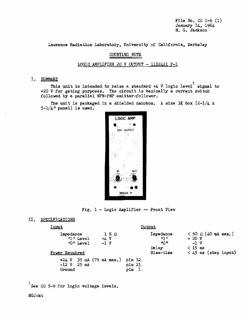
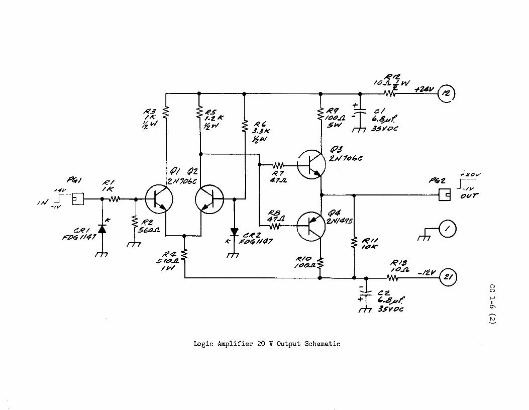
File No. CC 1-6 (1) January 14, 1964 H. G. Jackson
Lawrence Radiation Laboratory, University of California, Berkeley
COUNTING NOTE
LOGIC AMPLIFIER 20 V OUTPUT - 11X2421 P-1
I. SUMMARY This unit is intended to raise a standard +4 V logic level1 signal to
+20 V for gating purposes. The circuit is basically a current switch followed by a parallel NPN-PNP emitter-follower.
The unit is packaged in a shielded nanobox. A size JX box (2-1/4 x 5-1/4 11 panel) is used.
LOGIC AMP . '. 20V OUTPUT
. .., llX2420 Pl
Fig. 1 - Logic Amplifier -- Front View
II. SPECIFICATIONS Input
Impedance 1 K Q +4 v -1 v
Output Impedance
"l" "0"
Delay
< 50 Q ( 40 mA max. ) + 20 v 111 11 Level
110" Level
Power Required +24 V 35 mA (75 mA max.) -12 v 25 mA Ground
1 See CC 5-9 for logic voltage levels.
HGJ:mt
pin 12. pin 21. pin 1.
Rise-time
-1 v < 15 ns < 45 ns (step input)
~I
C/</ FPt;/147
R4 s it7..IJ. /W
l
4J4 V/14?5
Logic Amplifier 20 V Output Schematic
Y'20V
0 0
I-' I
°'
*
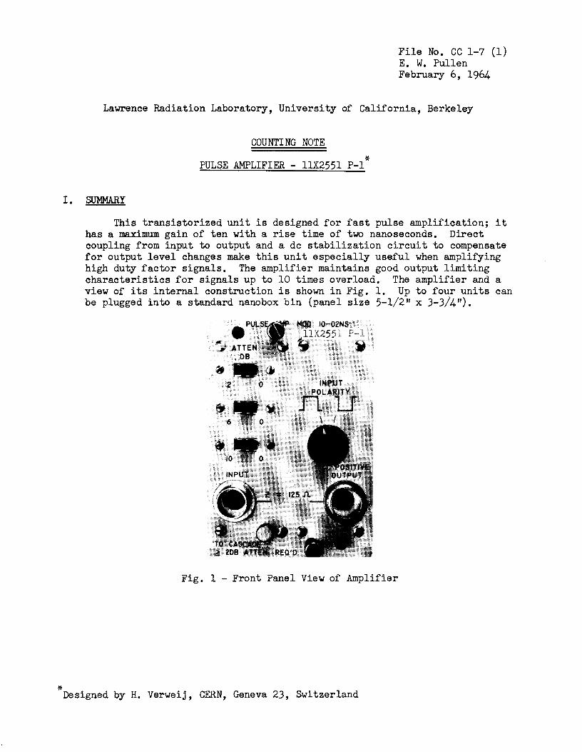
File No. CC 1-7 (1) E. W. Pullen February 6, 1964
Lawrence Radiation Laboratory, University of California, Berkeley
COUNT! NG NOTE
* PULSE AMPLIFIER - 11X2551 P-1
I. SUMMARY
This transistorized unit is designed for fast pulse amplification; it has a maximum gain of ten with a rise time of t'WO nanoseconds. Direct coupling from input to output and a de stabilization circuit to compensate for output level changes make this unit especially useful when amplifying high duty factor signals. The amplifier maintains good output limiting characteristics for signals up to 10 times overload. The amplifier and a view of its internal construction is shown in Fig. 1. Up to four units can be plugged into a standard nanobox bin (panel size 5-1/2 11 x 3-3/4").
.PULS
fl '.:,I ATTEN. DB •
2
~.,:MOD I0-02NS :., 11X2551 · ... :~ fj
INPUT POLARITY nu
Fig. 1 - Front Panel View of Amplifier
Designed by H. Verweij, CERN, Geneva 23, Switzerland

cc 1-7 (2)
II. SPECIFICATIONS
A. Input. 1. Positive or negative input pulses - ± 0.5 V for linear operation.
Maximum input amplitude ± 5.0 V. 2. Input impedance - 125 ohm. 3. Pulse polarity selected by a front panel control.
B. Output. 1. Positive pulses only. Maximum output + 5.0 V into 125 ohm load.
Overshoot is adjusted to less than 5% on both leading and trailing edges. A typical output waveform is shown in Fig. 2.
---+--
C. Gain.
-,-
a) Positive Input: Vert. - 200 mV/cm Hor. 5 ns/cm
b) Positive Input: Vert. - 200 mV/cm Hor. 1 ns/cm
c) Negative Input: Vert. - 200 mV/cm Hor. 5 ns/cm
Fig. 2 - Output Waveforms
1. Maximum gain: 10. Slide switch attenuators insert loss in the input giving the discrete gains shown in Table 1.
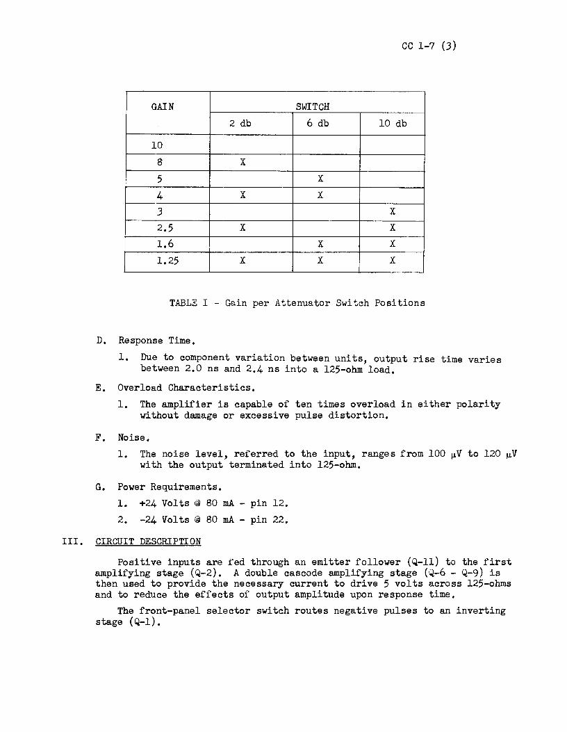
III.
cc 1-7 (J)
GAIN SWITCH 2 db 6 db 10 db
10 8 x 5 x 4 x x J x 2.5 x x 1.6 x x 1.25 x x x
TABLE I - Gain per Attenuator Switch Positions
D. Response Time. 1. Due to component variation between units, output rise time varies
between 2.0 ns and 2.4 ns into a 125-ohm load.
E. Overload Characteristics. 1. The amplifier is capable of ten times overload in either polarity
without damage or excessive pulse distortion.
F. Noise.
G.
1. The noise level, referred to the input, ranges from 100 µV to 120 µV with the output terminated into 125-ohm.
Power Requirements. 1. +24 Volts @ 80 mA - pin 12. 2. -24 Volts @ 80 mA - pin 22.
CIRCUIT DESCRIPTION
Positive inputs are fed through an emitter follower (Q-11) to the first amplifying stage (Q-2). A double cascade amplifying stage (Q-6 - Q-9) is then used to provide the necessary current to drive 5 volts across 125-ohms and to reduce the effects of output amplitude upon response time.
The front-panel selector switch routes negative pulses to an inverting stage ( Q-1).
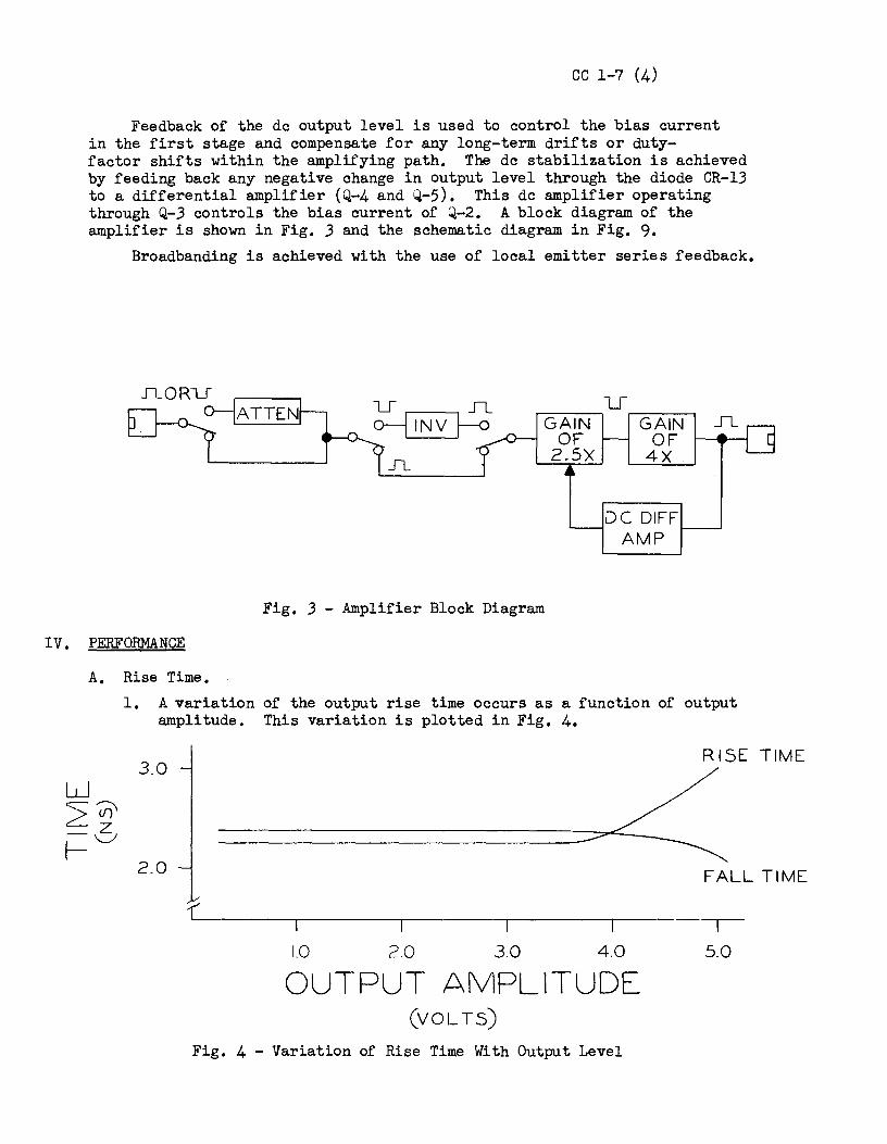
cc 1-7 (4)
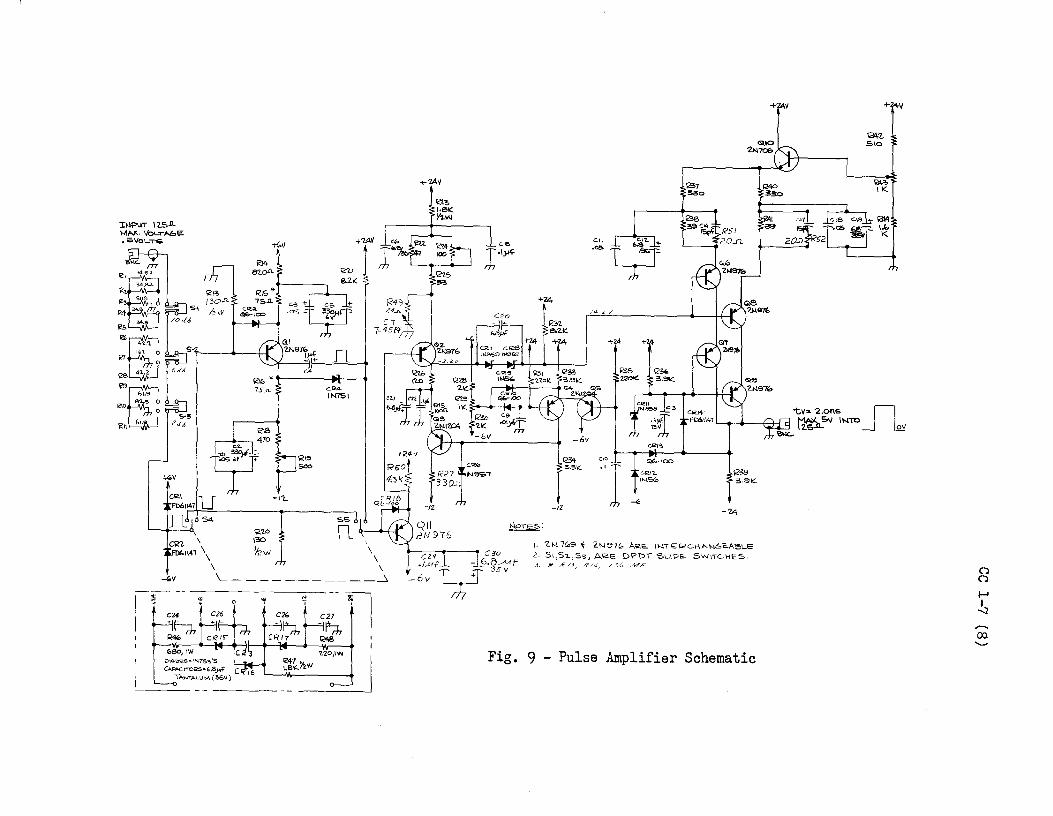
Feedback of the de output level is used to control the bias current in the first stage and compensate for any long-term drifts or duty-factor shifts within the amplifying path. The de stabilization is achieved by feeding back any negative change in output level through the diode CR-13 to a differential amplifier (Q-4 and ~-5). This de amplifier operating through Q-3 controls the bias current of Q-2. A block diagram of the amplifier is shown in Fig. 3 and the schematic diagram in Fig. 9.
Broadbanding is achieved with the use of local emitter series feedback.
ATTEN
Fig. 3 - Amplifier Block Diagram
IV. PERFORMANCE
A. Rise Time.
GAIN OF
4X
DC DIFF AMP
1. A variation of the output rise time occurs as a function of output amplitude. This variation is plotted in Fig. 4.
3.0
2.0
1.0 2.0 3.0 4.0
OUTPUT AMPLITUDE (VOL TS)
Fig. 4 - Variation of Rise Time With Output Level
RISE TIME
FALL TIME
--~
5.0
cc 1-7 (5)
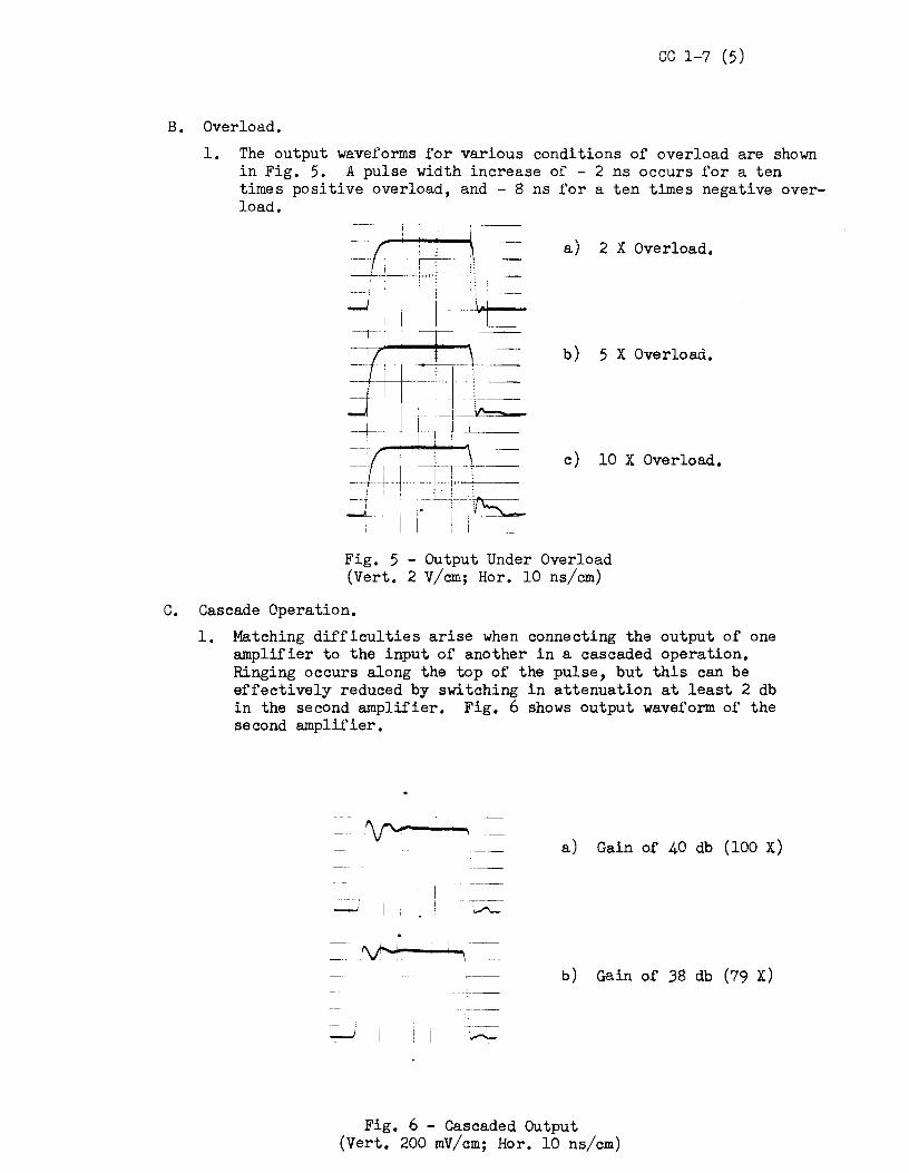
B. Overload. 1. The output waveforms for various conditions of overload are shown
in Fig. 5. A pulse width increase of - 2 ns occurs for a ten times positive overload, and - 8 ns for a ten times negative over-load.
a) 2 X Overload.
b) 5 X Overload.
c) 10 X Overload.
Fig. 5 - Output Under Overload (Vert. 2 V/cm; Hor. 10 ns/cm)
c. Cascade Operation. 1. Matching difficulties arise when connecting the output of one
amplifier to the input of another in a cascaded operation. Ringing occurs along the top of the pulse, but this can be effectively reduced by switching in attenuation at least 2 db in the second amplifier. Fig. 6 shows output waveform of the second amplifier.
a) Gain of 40 db (100 X)
b) Gain of 38 db (79 X)
! i
Fig. 6 - Cascaded Output (Vert. 200 mV/cm; Hor. 10 ns/cm)

cc 1-7 (6)
D. Duty Factor. 1. Fig. 7 shows the output for a burst of pulses at 20 MC pulse
rate. The burst length is 100 ms and burst rate is 50 cps.
a) Vert. 1 V/cm; Hor. 50 ns/cm.
b) Vert. lV/cm; Hor. 20 µs/cm
Fig. 7 - Output for a Burst Input
E. Pulse Width. 1. The output waveform for very long pulses experiences a droop due
to the feedb&ck effects of the de stabilization circuit. Fig. 8 shows this droop for a 15 µs input pulse.
Fig. 8 - Long Pulse Output (Vert. 1 V/cm; Hor. 2 µs/cm)

cc 1-7 (7)
REFERENCES
1. H. Verweij, "A Nanosecond Pulse Amplifier", Nuclear Instruments and Methods, Vol. 24 #1, p. 39 (July 1963)
2. UCLRL Drawing No. 11X2553 S-1.
EWP:mt
J:l-lf'\.IT \'2.5.IL I-JIM, \foL.-r"6E • 6VOL.\""S
-fOV
\ \ \
-11..
\ \
\ \ \__ ----------~
~24 ! C25 o
I µf=--J, I ~
G,801 tW
-12
q11 2N976
~
"e Cli t;:t r·IJA .. ·""'
+24
czo /¢.2 v R32
;µf e.21::: -t1'!- +211- -t24 ...
"""'
~-100
-12
J. '2.N 7(,,9 ' 2NS7G,, A12.e. \NTl<:l2C:l-\A.N6E.ABLE 2. s,,s.,_,s,., A12.E. Dl"PT SL.IDE. SWJTC-1-\E.S. 3. :It ft' /5_. h.'/6, /';'/a /WF.
Fig. 9 - Pulse Amplifier Schematic
+ v
tvs'2.ons n MA.>l SV IN.TO i'is.ll.. CV
'8WC..
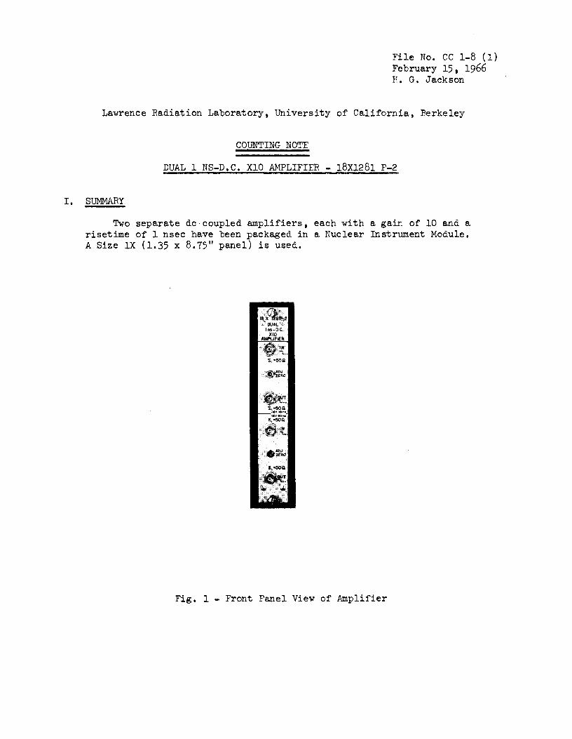
File No, CC 1-8 (1) February 15, 1966 H. G, Jackson
Lawrence Radiation Laboratory, University of California, Berkeley
COUNTING NOTE
DUAL 1 NS-D,C. XlO AMPLIFIER - 18Xl281 P-2
I, SUMMARY
Two separate de coupled amplifiers, each with a gain of 10 and a risetime of l nsec have been packaged in a Nuclear Instrument Module, A Size lX (l.35 x 8,75" panel) is used,
Fig, l - Front Panel View of Amplifier
II. SPECIFICATIONS
Gain Risetime Input impedance Input polarity Output polarity Maximum output amplitude Delay, input to output Equivalent noise level at input Thermal drift of output level
Power Required
+12 v 30mA -12 v 90mA Ground
III. CIRCUIT DESCRIPTION
pin 16. pin 17. pin 34.
10 1 nsec 50 ohms Negative Negative 1 V in 50 ohms 3 nsec 50 uV rms 1 mV/°C
cc 1-8 (2)
A schematic diagram is shown in Fig. 2. Two transistors are used in a feedback configuration to give a typical closed-loop gain of 11. The open loop gain is about 66.
The trimmer capacitor (C-3) provides high-frequency compensation. The potentiometer (R-6) is a front panel control used to adjust the output level tc 0 V.
With the negative input signals the currert in Q-1 decreases and that in Q-2 increases. The 1N753A (CR-3) is quiescently conducting 20mA, which decreases as the current in Q-2 increases. With zero current in CR-3, its impedance is very large, thereby substantially reducing the gain of 0.-2. In this way the amplifier output current is limited to about 20mA or 1 V into a 50-ohm load. In practice the saturated output is about 1.5 V,
Inclusion of CR-1 is an attempt to perform some temperature compensation for the base-emitter junction of Q-1. Its effect is to hold the output de level change with temperature to less than 1 mV/°C. Typically, over the temperature range 20 to 75°c, the output level changes less than 25 mV.
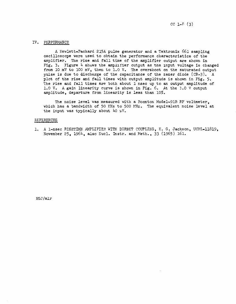
cc 1-8 (3)
IV, PERFORMANCE
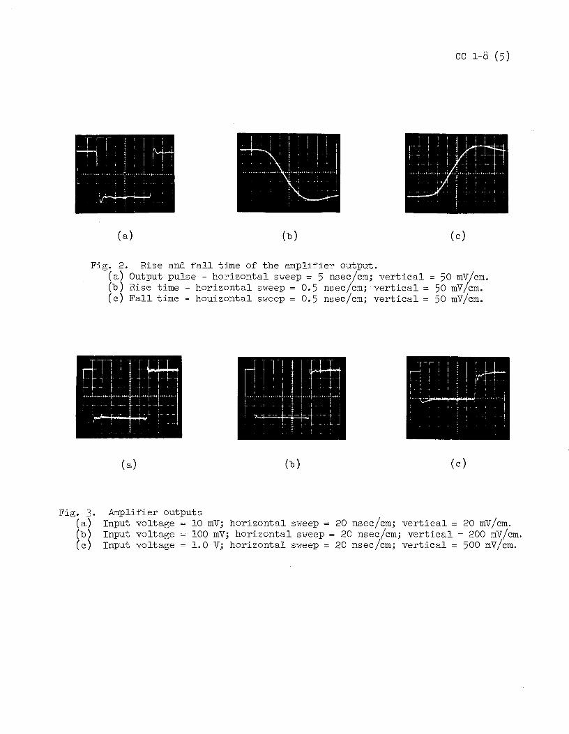
A Hewlett-Packard 215A pulse generator and a Tektronix 661 sampling oscilloscope were used to obtain the performance characteristics of the amplifier, The rise and fall time of the amplifier output are shown in Fig, 3, Figure 4 shuws t.he ampJ.11'1er output as the input voltage is changed from 10 mV to 100 mV, then to 1.0 V. The overshoot on the saturated output pulse is due to discharge of the capacitance of the zener diode (CR-3). A plot of the rise and fall times with output amplitude is shown in Fig. 5, The rise and fall times are both about 1 nsec up to an output amplitude of 1.0 V. A gain linearity curve is shown in Fig, 6. At the 1.0 V output amplitude, departure from linearity is less than 10%,
The noise level was measured with a Boonton Model-91B RF voltmeter, which has a bandwidth of 50 KHz to 500 MHz. The equivalent noise level at the input was typically about 40 JJV.
REFERENCES
1. A 1-nsec RISETIME .AMPLIFIER WITH DIRECT COUPLING, H, G. Jackson, UCRL-11819, November 25, 1964, also Nucl. Instr. and Meth., 33 (1965) 161,
HGJ/mlr
PGI BNC
Input L_ __ _
RG-174/U
+12 v
2N2857
-12 v
LI Iµ. H
R2 820.0.
Trim aeon R5 511.0. MF
R9 2.7K
cc 1-8 (4)
PG2 RS RG-174/U
348.\1 ...-~1:-+~~~~~~-t:::H BNC
Output MF
CR2 IN959B
L2 10µ.H
RIO 220 .a
CR3 IN753A
L_ __ _
MU B-4895
Fig. 2 - Schematic of the Amplifier
cc 1-8 (5)
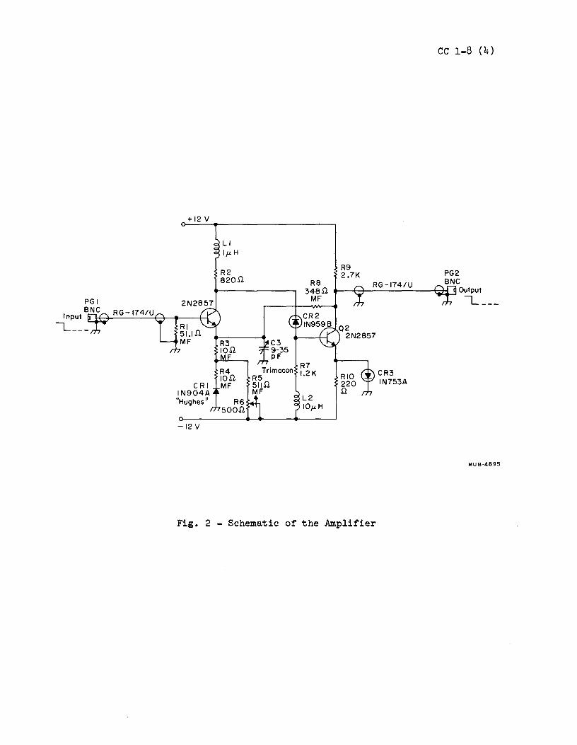
Ff-Tl 1 l-r.·--.--1 r • 1 1 r F11 . - • t • f * t 1 • • • '-·• • • • • ··~ • < '·•·H 1 ,.., ' •·I·!·.• t ! ' :.; ' • l ; l f*·• • • •·' •
t
(a) (b) (c)
Fig. 2. Rise and fall time of the amplifier output. (a) Output pulse - horizontal sweep= 5 nsec/cm; vertical = 50 mV/cm. (b) Rise time - horizontal sweep= 0.5 nsec/cm; vertical= 50 mV/cm. (c) Fall time - houizontal sweep= 0.5 nsec/cm; vertical= 50 mV/cm.
rt_-_-·-·r·1 1 r .. ~ ·J f I 4-l rt~1
I . I I l I I I /+H+i+HHH..;++Htt->H •+t_+--H~t+H+j+H+fH·H
I' I I j 1 : i
1,. ·- ' T -: : _( • I -~ •~- -I t. l
' j
,_ .. t
(a) (b) (c)
Amplifier outputs Fig. 3. (a) (b) (c)
Input voltage 10 mV; horizontal sweep= 20 nsec/cm; vertical= 20 mV/cm. Input voltage = 100 mV; horizontal sweep= 20 nsec/cm; vertical = 200 mV/cm. Input voltage = 1.0 V; horizontal sweep= 20 nsec/cm; vertical= 500 mV/cm.
cc 1-8 (6)
4.0
3.0 - Rise (.) Q.) (/) c -Q.) 2.0 E r
I. 0
0 ---~~-'-~~-'-~~--1.~~~.._~~~~~-'-~~~..__~~~ 0 0.2 0.4 0.6 0.8 1.0 1.2 1.4 1.6
Vout (V)
MU B-4894
Fig. 5 - Rise and Fall Time vs Output Voltage

cc l-8 (7)
/ I. 2 /
/ /
/ /
/ 1.0 /
/ /
0.8
-> 0.6
+-::J 0
> 0.4
0.2
0 ,.__~~..__~~....I...-~~ ........ ~~--'-~~--'~~~'--~~.....__~~_._~~-' 0 20 40 60 80 100 120 140 160 180
Vin (mV) MU B-4893
Fig. 6 - Gain Linearity Curve
File No. CC 2-lB (1) Q. Kerns; F. Kirsten; C. Winningstad Rev. July 29, 1966 F. Kirsten and R. Wallace
Lawrence Radiation Laboratory, University of California, Berkeley
COUNTING NOTE
PULSE RESPONSE OF COAXIAL CABLES
I. ABSTRACT
For most cables useful in counting work, attenuation below approximately 1000 me is due mainly to skin-effect losses and varies as the square root of frequency. For such cables the step-function response has a rise time that varies as the square of the attenuation at a given frequency. Curves are given to aid in the selection of cables for transmitting nanosecond pulses.
II. STEP FUNCTION RESPONSE Mathematically ideal, lossless coaxial cables can be shown to transmit
electrical pulses in the TEM mode without attenuation or distortion. How-ever, all physically realizable cables have losses, the magnitude of which changes with frequency. Pulses transmitted through such cables suffer both attenuation and distortion. By means of the Laplace transform, the nature of the distortion can be calculated if the attenuation and phase-shift are known at all frequencies. In most of the cables presently useful in count-ing work, skin effect losses in the conductors are the predominate losses below about 1000 me. Skin-effect losses produce an attenuation whose magnitude in decibels varies as the square-root of frequency. This results in a step function response of:
where E out
j b
A
erf
b ,e Eout = Ein (l - erf V 2 (t-'f))
= voltage at dista~ce J. from input end of semi-infinitely long uniform cable,(lJ at time t (seconds).
= amplitude of step of voltage applied to input of cable at time t = o.
= distance from input end in feet, • constant for the particular cable in question.
-8 -1 l = 1.45 x 10 A - feet sec 2
= attenuation of cable at 1000 me - db/100 feet (attenuation figures for coaxial cables are commonly quoted in these units).
= error function( 2 ) = transit time of cable defined as the value of t at which the
voltage at..Q first begins to change (considering only the step function occurring at t = o, of course).
(l)With negligible error in most cases E t can be taken as the response at the receiving end of a cable of length1, 0 ¥erminated in a resistor equal to its characteristic impedance.
(2)As defined in Reference l, p 256.
cc 2-lB (2)
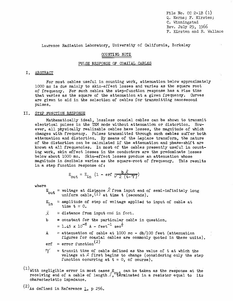
Fig. 1 may clarify the nomenclature involved in this relation.
Fig. 1 - This illustrates the space relation between E. and E t• l.n OU
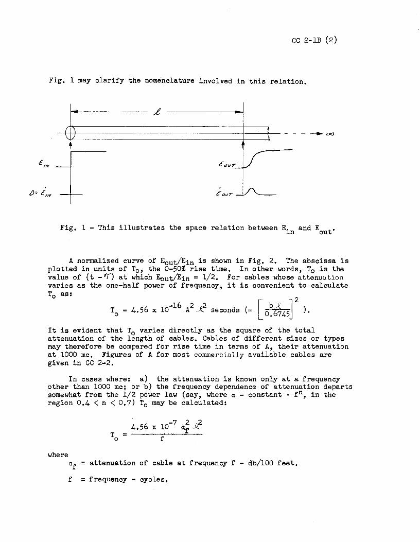
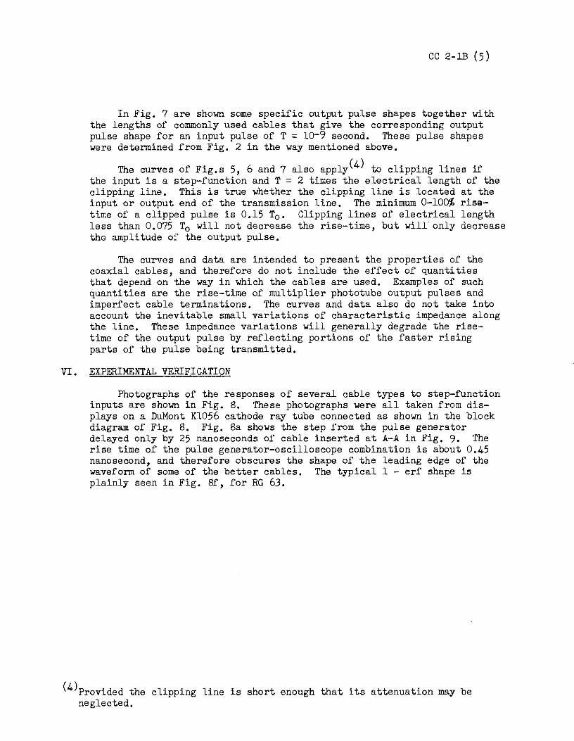
A normalized curve of Eout/Ein is shown in Fig. 2. The abscissa is plotted in units of T0 , the 0-50% rise time. In other words, T0 is the value of (t -d/) at which Eout/Ein = 1/2. For cables whose attenuation varies as the one-half power of frequency, it is convenient to calculate T0 as:
[ ~2
-16 2 2 b.J T0
= 4.56 x 10 A .)( seconds (= 0 •6745 ).
It is evident that T0 varies directly as the square of the total attenuation of the length of cables. Cables of different sizes or types may therefore be compared for rise time in terms of A, their attenuation at 1000 me. Figures of A for most commercially available cables are given in CC 2-2.
In cases where: a) the attenuation is known only at a frequency other than 1000 me; or b) the frequency dependence of attenuation departs somewhat from the 1/2 power law {say, where a = constant • fn, in the region 0.4 < n < 0.7) T0 may be calculated:
where af = attenuation of cable at frequency f - db/100 feet.
f = frequency - cycles.
cc 2-lB (3)
In case a) the nomogra.m of Sec. VII CC 2-2 may be useful• In case b), it has been empirically determined that reasonably accurate results are obtained where f is the frequency at which the total attenuation (i.e., af J'/100) of the cable is 6 decibels, Substituting af .f/100 = 6 db into the above gives the useful relation
where f 6 =frequency at which the total attenuation of the length of
cable in question is 6 db.
The times to reach other precentages of the input step amplitude are given in Table I.
TABLE I RISE TIME CONVERSION FACTORS
0 to X ~ rise time x To
10 0.17 20 0.28 50 1.0 70 3.1 80 7.3 90 29. 95 110.
The 10 to 90% rise time is thus (29 - 0.17) T = 28.83 T0
• 0
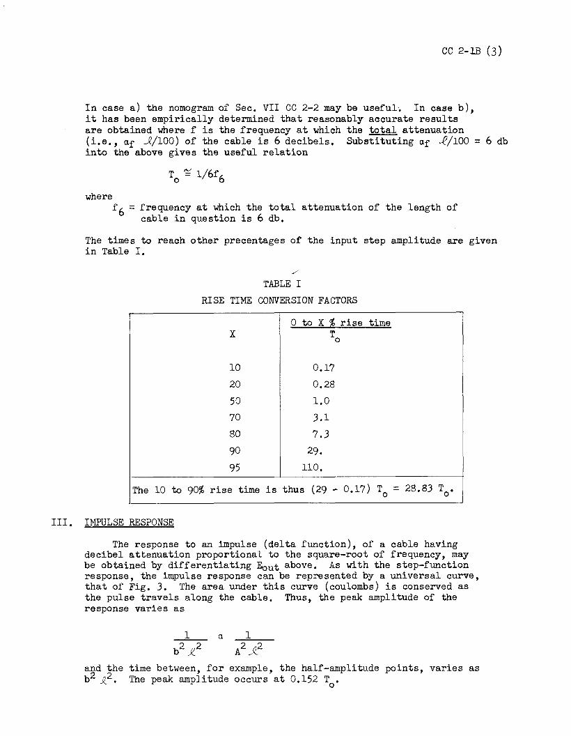
III. IMPULSE RESPONSE
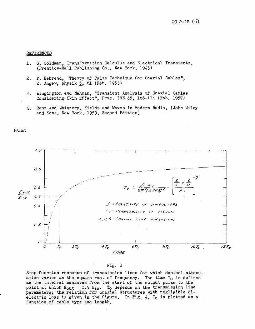
The response to an impulse (delta function), of a cable having decibel attenuation proportional to the square-root of frequency, may be obtained by differentiating Eout above. As with the step-function response, the impulse response can be represented by a universal curve, that of Fig. J. The area under this curve (coulombs) is conserved as the pulse travels along the cable. Thus, the peak amplitude of the response varies as
1
and the time between, for example, the half-amplitude points, varies as b2 f!._2. The peak amplitude occurs at 0.152 T •
0
cc 2-lB (4)
IV. fiESPONSE TO OTHER PULSE SHAPES
It will be noted that, since the rise time T is proportional to ...R....2 , if two equal lengths of a given type of cable are0 cascaded, the rise time of the combination is four times the rise time of either length alone. This is in contrast to the well-known case of amplifiers of "Gaussian" frequency response, in which the rise time varies as the square root of the number of identical sections. For this reason, and also because the characteristic step-or impulse-function responses of cables and of "Gaussian" amplifiers are so different, the rule-of-thumb that the over-all rise time= .}sum of squares of individual rise times is not applicable either with cables alone, or where cables are combined with Gaussian elements. Instead, the overall response of a system with cables and other elements may b~ obtained graphically or with the standard con-volution integrals(3J using either the step-or impulse-function response of the cables.
V. RECTANGULAR PULSE RESPONSE, CLIPPING LINES
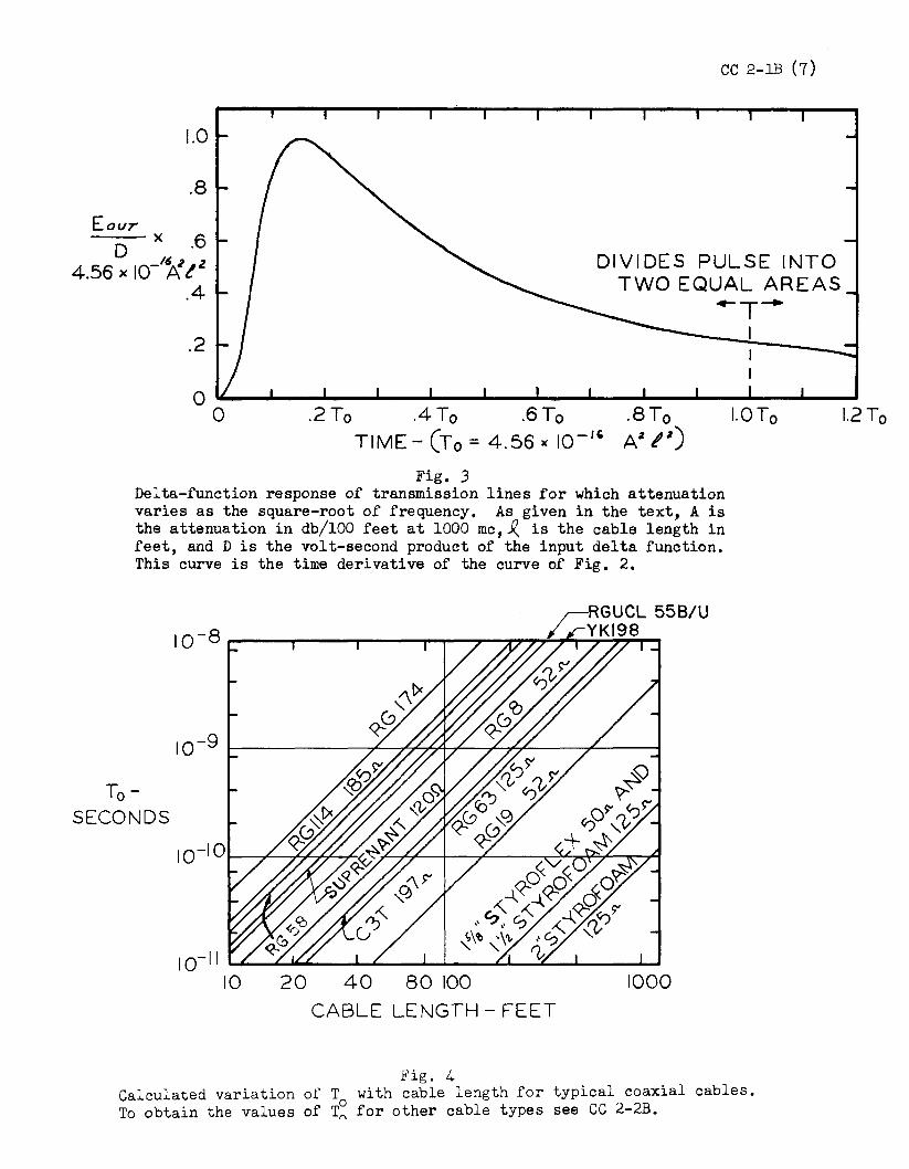
The response of a cable to a rectangular pulse of a duration T can be found by a simple application of superposition. The rectangular pulse is considered to consist of a positive step-function at t = O, followed by a negative step-function at t = T. The amplitude reduction of such a pulse as a function of the distance it has traveled along the selected coaxial cables is shown in Fig.s 5, 6 and 7. Fig. 5 includes a curve showing the time-stretching of the output pulse with respect to the input pulse. ·By suitably changing the length scale in the way indicated on the figure, the two curves of Fig. 5 can be applied to any pulse duration and any cable for which attenuation varies as the square root of frequency. The amount of time-stretching of any output pulse can therefore be deter-mined from Fig. 5 by knowing the value E0 ut/Ein for the pulse, where E t is the peak amplitude of the output pulse, and Ein is the amplitude ou of the input pulse.
The relative merits of various coaxial cables as conductors of pulses from multiplier phototubes or other current generators can be estimated from the curves of Fig. 6 which are replotted from Fig. 5. Use Fig. 6a for pulses of T = l0-8 second; 6b for T = l0-9; 6c for T = lo-10. Note that the input is a rectangular current pulse of 1 ampere amplitude. At the input end of the cable, therefore, the voltage amplitude of the rectangular pulse is Zo volts, where Z0 is the characteristic impedance of the line. The curves show, for example, that for an input current pulse of T = 10-9 second, the peak voltage of the output pulse at the end of a 75 foot run of RG 114 would be the same as that at the output end of a 75 foot run of RG 63, even though the voltage developed at the input end of the RG 114 would be 185/125 times the voltage at the input of the RG63.
(J)Reference 1, pp 112-120
cc 2-lB (5)
In Fig. 7 are shown some specific output pulse shapes together with the lengths of commonly used cables that give the corresponding output pulse shape for an input pulse of T = 10-9 second. These pulse shapes were determined from Fig. 2 in the way mentioned above.
The curves of Fig.s 5, 6 and 7 also apply(4 ) to clipping lines if the input is a step-function and T = 2 times the electrical length of the clipping line. This is true whether the clipping line is located at the input or output end of the transmission line. The minimum 0-100% rise-time of a clipped pulse is 0.15 T0 • Clipping lines of electrical length less than 0.075 T0 will not decrease the rise-time, but will only decrease the amplitude of the output pulse.
The curves and data are intended to present the properties of the coaxial cables, and therefore do not include the effect of quantities that depend on the way in which the cables are used. Examples of such quantities are the rise-time of multiplier phototube output pulses and imperfect cable terminations. The curves and data also do not take into account the inevitable small variations of characteristic impedance along the line. These impedance variations will generally degrade the rise-time of the output pulse by reflecting portions of the faster rising parts of the pulse being transmitted.
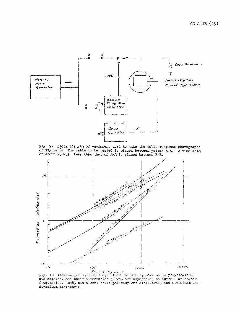
VI. EXPERIMENTAL VERIFICATION
Photographs of the responses of several cable types to step-function inputs are shown in Fig. 8. These photographs were all taken from dis-plays on a DuMont Kl056 cathode ray tube connected as shown in the block diagram of Fig. 8. Fig. 8a shows the step from the pulse generator delayed only by 25 nanoseconds of cable inserted at A-A in Fig. 9. The rise time of the pulse generator-oscilloscope combination is about 0.45 nanosecond, and therefore obscures the shape of the leading edge of the waveform of some of the better cables. The typical 1 - erf shape is plainly seen in Fig. 8f, for RG 63.
(4)Provided the clipping line is short enough that its attenuation may be neglected.
cc 2-lB ( 6)
REFERENCES
1. s. Goldman, Transformation Calculus and Electrical Transients, (Prentice-Hall Publishing Co., New York, 1945)
2. P. Behrend, "Theory of Pulse Technique for Coaxial Cables", z. Angew, physik ~' 61 (Feb. 1953)
3. Winging ton and Nahman, "Transient Analysis of Coaxial Cables Considering Skin Effect", Proc. IRE !t2., 166-174 (Feb. 1957)
4. Ramo and Whinnery, Fields and Waves in Modern Radio, (John Wiley and Sons, New York, 1953, Second Edition)
FK:mt
/,()
08
06 Eour E IN 0 s-
04
0 2
0
I I
- -------·
I
.1
6To BTo /()7;, TIME
Fig. 2 Step-function response of transmission lines for which decibel attenu-ation varies as the square root of frequency. The time T0 is defined as the interval measured from the start of the output pulse to the point at which E0 ut = 0.5 Ein• T0 depends on the transmission line parameters; the relation for coaxial structures with negligible di-electric loss is given in the figure. In Fig. 4, T0 is plotted as a function of cable type and length.
cc 2-lB (7)
1.0
.8
Eovr D x .6
4.56 x 10-'~2 l z .4
DIVIDES PULSE INTO TWO EQUAL AREAS
~T_.
.2
0 0 .2To .4To .6To .8To
TIME - (To= 4.56 >< 10-" Az !z) Fig. J
Delta-function response of transmission lines for which attenuation varies as the square-root of frequency. As given in the text, A is the attenuation in db/100 feet at 1000 me,~ is the cable length in feet, and D is the volt-second product of the input delta function. This curve is the time derivative of the curve of Fig. 2.
To-SECONDS
10-ll --~,__--~----~--'--~--~----~~........-10 20 40 80 100 1000
CABLE LENGTH - FEET
Fig. 4
I
l.OTo
Calculated variation of T with cable length for typical coaxial cables, To obtain the values of T~ for other cable types see CC 2-2B.
l.2To
i.o
0.8
0.6 EouT
E1N 0.4
cc 2-lB (8)
4
3
2
0.21--------------------------
r..-~--a.--~~-'-----i.--~-------~..1..-~--11....-------.....-----,,__~~ 0
T1 -T
0 40 100 200 400 800 lOOO
A f_ v'io-9/T 10,000 40,000
Fig. 5
The time-stretching and amplitude-reduction of an originally rectangular pulse plotted as a function of A, the attenuation of the cable at 1000 me in db/100 ft.;~' the length in feet; and T, the duration of the input pulse in seconds. Attenuation figures may be obtained from CC 2-2B. As an example, for RG63, A is 7 db/100 ft. Thus if T were lo-9 sec, and..e were 100 feet, the chart should be entered at an abcissa of 700.

cc 2-lB (9)
200 IA~nT=I0-8 C3T
w 160 l.9 <t I-_J STYROFOAM 0 120 > I-::) Q.. I-::) 0
80
~ RGl9 <t w
0... 40 RGUCL55B
0 100 150 200 250 0 50
CABLE LENGTH - FEET
Fig. 6(a)
200 _j_ T=-10-9 SEC
!AMP-fl
T w 160 <..9 <t: .._ _J 2" ST YR0FOAM 0 > 120 .._ ::::> (L .._ ::> 80 0
:::s::: <t: w ANDREW a_ 40
RGl9
RGUCL55
0 0 50 100 150 200 250
CABLE LENGTH - FE ET

cc 2-1.B (10)
200 IA~fl T= 10-IOSEC
w <.9 160 <( I-_J 0 > STYROFOAM I- 120 :::::> 0.. I-:::::> 0 80 ::s:: <( w 0..
40
0 0 50 100 {50 200 250
CABLE LENGTH - FEET
Fig. 6(c)
Peak amplitude or the output voltage pulse from some typical coaxial cables as a function of cable length. The assumed inputs are rec-tangular current pulses of 1 ampere amplitude and durations of 10-8 1 io-9 and io-10 seconds. These curves are all replotted from Fig. 5 with suitable scale changes.

~ T f-,- -1 ,-, i-- -, i-- -,
I I I I I I I I I I I I
I I I I I I I I
I I J '- I_ L ~ ~ INPUT PULSE (a} (b} (c} (d} (e}
For T = 10-9 sec., the output pulse will have the shape and amplitude shown for the following cable lengths.
CABLE TYPE (a) (b) (c) (d) (e)
RG174 23 41 67 90 110 RG58 30 56 93 136 156 RG8 77 145 240 350 400 RG63 95 180 290 430 500 2"Styrofoam 1200 2300 3700 5500 6400 C3T 90 170 280 4oo 470 RG114 37 70 110 170 200 RGUCL 55B/U 39 73 118 174 203 YK198 46 88 142 211 245
Fig. 7 The above waveforms show the deterioration of an originally rectangular pulse as it travels along a transmission line for which the decibel attenuation varies as the square root of frequency. For comparison purposes, the input pulse is also shown with each output wave-form. The figures listed above give the cable lengths that will cause the distortion shown when T= lo-9 second. To find the cable lengths for which the output pulse will have the same form relative to the input pulse for other input pulse durations, multiply the above lengths by T, where T is the input pulse duration in millimicroseconds. 0
0 I\) I
bj
I-' I-'

cc 2-lB ( 12)
mus •
•
IFfPtl I
ot Ll<.LLHt::;a
GU~>t!LLO!:l'-''-'"'U ... _.,,.,.,. used tube. a) Pulse "".!JJ1J.i..1.1:1u.
output end ot • Frequency ot
.,...,,, ... .., same time sea.le as cathode-ray tube d.istortion. made by
a zero reference.
- ; d = mus.
M,.rr;U"'1 f"v/IHI t:;-rnft.f'<>f,,.,.
A
L 8 B
cc 2-lB (13)
A 0 ~'I"----<.------ --·1
Cablu /c,,..,,,,.111>f'A,,
Trl.
J,__ .5w,.r.,o : . c;,~, .. ,~,.,...,,Jor •--------
Tr'9· =----
·-· 1
CaT/1A:.1J:1 - C.1y 'Tub~
L'u,,,o,,f 7!1,c>e K /0$"6
Fig. 9. Block diagram of equipment used to take the cable response photograph::; of Figure 8. The cable to be tested is placed between points A-A. A time dela, of about 25 mus. less than that of A-A is placed between B-B.
10 10(; /C)~10 /Cl,000
,.::-1· .;:,_">; .'I .: i - / ..; Fig. 10 Attenuation vs frequency. · Eotn RG6 anc 19 nave sol id polye'thylene dielectrics, and their attenuation cuc1es are asympt.otic to cu:ve ,, at higher frequencies. RG63 has a se:ni-colid poL·etnylene diele;c.ric, and Styrofoam usei Styrofoam dielectric.
File No. CC 2-2C (1) F. Kirsten and L. Proehl Rev. May 31, 1966 F. Kirsten and R. Wallace
Lawrence Radiation Laboratory, University of California, Berkeley
GOU NTING NOTE
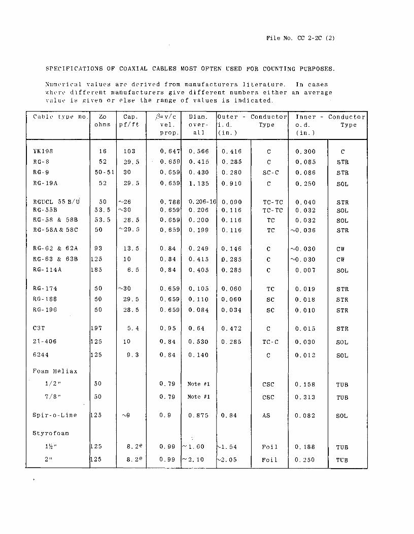
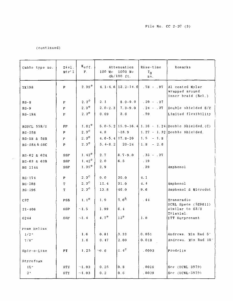
PHYSICAL CHARACTERISTICS OF COAXIAL CABLES
Listings of some of the physical properties of certain commercially available coaxial cables and delay lines are given. The cables listed are those considered to be most probably applicable to counting work. Most of the numbers are taken from manuf acturer 1s literature.
Following the cable listings is a section in which other properties and characteristics of dielectrics and coaxial transmis~ion lines are given.
TABLE OF CONTENTS
I. Cable types most often used for counting purposes. Brief specifications included •••••••••••••••••••••••••••••••••••• 2
II. Cable types of possible use for counting purposes.
III. IV. v.
VI. VII.
VIII.
A. Listed by RG n\llD.bers • • • • • • • . • • • • • • • . • • • • • • • • • • • • • • • • • • • • • • • • • 7 B. Miniature types, (o.d. less than 0.191 inches) • • • • • • • • • • • • • • • 10 c. Rigid and Semi-Rigid types•••·••••••••••••••••••••••••••••••• 11 D. Delay cables . . . . . . . . . . . . . . . . . . . . . ... . . . . . . . . . . . . . . . . . . . . . . . . . . 12
Properties of dielectrics used in coaxial cables••••••••••••••••• Temperature coefficient of length of certain cables •••••••••••••• Noise characteristics of cables •••••••••••••••••••••••••••••••••• Chart for converting attenuation data to risetime . .............. . Nomograph for computing coaxial transmission-line impedance •••••• Transmission line formulas •••••••••••••••••••••••••••••••••••••••
1.3 14 14 15 16 17
File No. CC 2-2C (2)
SPECIFICATIONS OF COAXIAL CABLES MOST OFTEN USED FOR COUNTING PURPOSES.
Numerical values are derived from manufacturers literature. In cases where different manufacturers give different numbers either an average value is given or else the range of values is indicated.
Cable type no. Zo Cap. ,B= vi c Diam. Outer - Conductor Inner - Conductor ohms pf/ft vel. over- i. d. Type 0. d. Type
prop. all (in. ) (in. )
YK198 16 103 o. 647 0. 566 0. 416 c 0. 300 c RG-8 52 29. 5 0. 659 0. 415 0. 285 c 0.085 STR RG-9 50-51 30 0.659 0. 430 0. 280 SC-C 0.086 STR RG-19A 52 29. 5 0.659 1. 135 0.910 c 0. 250 SOL
RGUCL 55 B/U 50 "-'26 o. 788 0.206-16 0.090 TC-TC 0.040 STR RG-55B 53. 5 "-'30 0. 659 0. 206 0. 116 TC-TC 0.032 SOL RG-58 & 58B 53. 5 28. 5 0.659 0.200 0. 116 TC 0.032 SOL RG- 58A & 58C 50 "-'29. 5 0.659 0. 199 0. 116 TC "-'0.036 STR
RG-62 & 62A 93 13. 5 0. 84 0. 249 0. 146 c "-'0.030 cw RG-63 & 63B 125 10 0.84 0. 415 0. 285 c "-'0.030 CW RG-114A 185 6. 5 0.84 0. 405 0. 285 c 0.007 SOL
RG-174 50 "-'30 0. 659 0. 105 0. 060 TC 0.019 STR RG-188 50 29. 5 o. 659 0. 110 0.060 SC 0.018 STR RG-196 50 28. 5 0. 659 0.084 0.034 SC 0.010 STR
C3T 197 5. 4 0.95 0. 64 0.472 c 0.015 STR
21-406 125 10 0.84 0. 530 0. 285 TC-C 0.030 SOL
6244 125 9. 3 0.84 0. 140 c 0.012 SOL
Foam Heliax
1/2" 50 0.79 Note #1 csc 0. 158 TUB
7 /8" 50 0. 79 Note #1 csc 0. 313 TUB
Spir-o-Line 125 -v9 0.9 0.875 0.84 AS 0.082 SOL
Styrofoam
1 \12" 125 8. 2e 0.99 ~ 1. 60 tvl. 54 Foil 0. 188 TUB
2" 125 8. 2e 0.99 ~ 2. 10 ~2.05 Foil 0. 250 TUB
File No. CC 2-2C (3)
(continued)
Cable type no. Diel. Keff. Attenuation Rise-time Remarks Mtr' 1 F. 100 Mc 1000 Mc To
db/100 ft. ns.
YK198 p 2. 39 e 4.1-4.6 13.2-14.6 .78 - . 97 Al coated Mylar wrapped around inner braid (Bel.)
RG-8 p 2. 3e 2. 1 8. 0-9. 0 . 29 - . 37
RG-9 p 2. 3 e 2. 0-2. 3 7.3-9.0 . 24 - . 37 Double shielded 8/U
RG-19A p 2. 3e 0.69 3. 6 . 59 Limited flexibility
RGUCL 55B/U FP 1. 61 e 5. 0-5. 2 15.9-16.4 1. 16 - 1. 24 Double Shielded, (C)
RG-55B p 2. 3e 4.8 "'16.9 1. 27 - 1. 32 Double Shi el ded.
RG-58 & 58B p 2. 3e 4.6-5.4 17.8-20 1. 5 - 1. 8
RG- 58A & 58C p 2. 3e 5.4-6.2 20-24 1 . 8 - 2.6
RG-62 & 62A SSP 1. 42e 2.7 8. 7-9. 0 . 35 - . 37
RG-63 & 63B SSP 1. 42e 2.0 6. 5 . 19
RG- ll 4A SSP 1. 35e 2.9 .39 Amphenol
RG- 17 4 p 2. 3e 9.0 30.0 4. 1
RG-188 T 2. 3e 11. 4 31. 0 4. 4 Amphenol
RG-196 T 2. 3e 13. 8 46.0 9.6 Amphenol & Microdot
C3T PSB 1. 1 e 1. 9 7.6-k .44 Transradio UCRL Specs ( 5Z9611)
21-406 SSP "'l. 5 1.99 6.4 similar to 63/U Tri axial.
6244 SSP <vl. 4 4.7e 15e 1. 0 ITT Surprenant
Foam Heliax
1/2" 1. 6 0. 81 3. 33 0.051 Andrews. Min Rad 5"
7/8" 1. 6 0. 47 2.00 0. 018 Andrews. Min Rad 10"
Spir-o-Line PT 1. 2 5 "'0. 6 1. 4e . 0093 Prodelin
Styrofoam
1 Yz" STY 'Vl. 0 3 0. 25 0. 8 . 0016 See (UCRL-3579) 2" STY "'l.03 0. 2 0.6 .0029 See (UCRL-3579)
DIELECTRIC MATERIAL CODING
FP --------- Polyethylene foam P ---------- Polyethylene PC --------- Polyvinyl chloride PS --------- Polystyrene PSB -------- Polystyrene beads PT --------- Polyethylene tubes SP --------- Polyethylene spiral SSP -------- Semi-solid polyethylene ST --------- Teflon Spiral STY -------- Styrofoam T ---------- Teflon TPS -------- Polystyrene tape TT --------- Teflon tape
INNER AND OUTER CONDUCTOR CODING
Al ------- Aluminum AS ------- Solid aluminum C -------- Copper CSC ------ Corrugated solid copper Cu ------- Copper CW ------- Copper weld Foil ----- Tin Cu foil wrapped & over-
lapped SC ------- Silvered copper SOL ------ Solid STR ------ Stranded TC ------- Tinned copper TUB ------ Copper tubing
Note # 1. Without jacket With jacket
Note # 2. Without jacket With jacket
o.d. 0.540 o. d. 0.660
o. d. 0.980 o. d. 1. 100
File No. CC 2-2C (4)
MANUFACTURERS CODING
Amp -- - - Amphenol-Borg Electronics Corp. An - - - - - Andrew Corp. c ------ Chester Cable Corp. ITTR -- - Inter. Tele. & Tele. Royal ITTS - -- Inter. Tele. & Tele. Surprenant M ------ Microdot Inc. Prod - -- Prodelin TR -- - - - Transradio Ltd. Bel - -- - Belden
NOTE CODING
e -------f -------h -------j -------k
Calculated Effective dielectric constant, 1//32 Measured at 400 Mc. Measured in micromicrofarad per foot. Measured at 600 Mc.
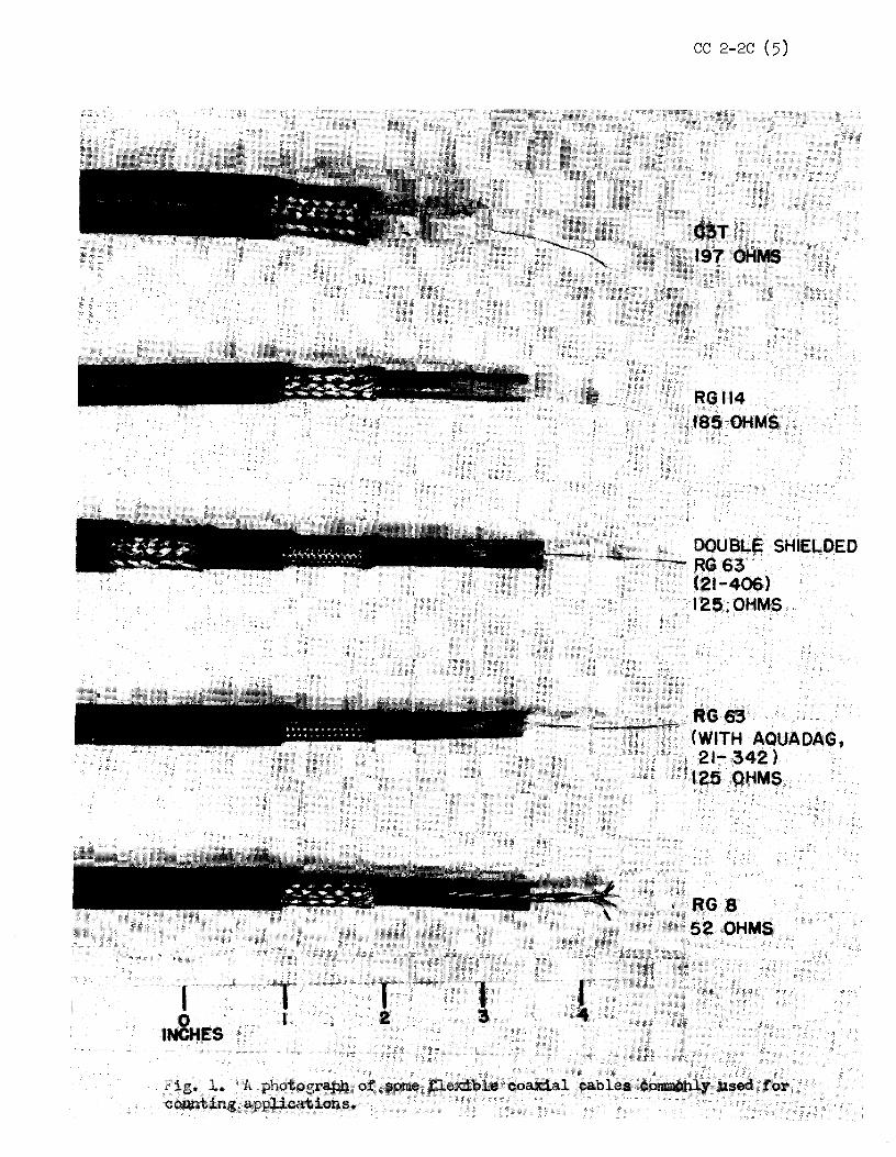
CC 2-2C (5)
RGl14 t85 OHMS
DOUBLE SHIELDED ~'."~···""'....,.,, __ .....::.:::.., RG 63
' '
··1 1r&Es
... l I
·r·· · .... -.4"········~···1 .. ······· ··· · · · ·· ............. l ............ . 2 3 4
l. A photograph sotlle counting. applie.s;t..iona.
(21-406) 125 OHMS
RG63 (WITH AQUAOAG, 21- 342)
125 OHMS
, RG 8 · 52 OHMS
··;

. ' 0 I I 2 ' s ' 4
INCHES
l I I •
CC 2-2C (6)
STYROFOAM 125 OHMS
RG 19 52 OHMS
STYROFLEX 50 OHMS
Fig. 2. Photographs showir..g the construction of some rigid and semi-rigid coaxial transmission lines.
File No. CC 2-2C 17)
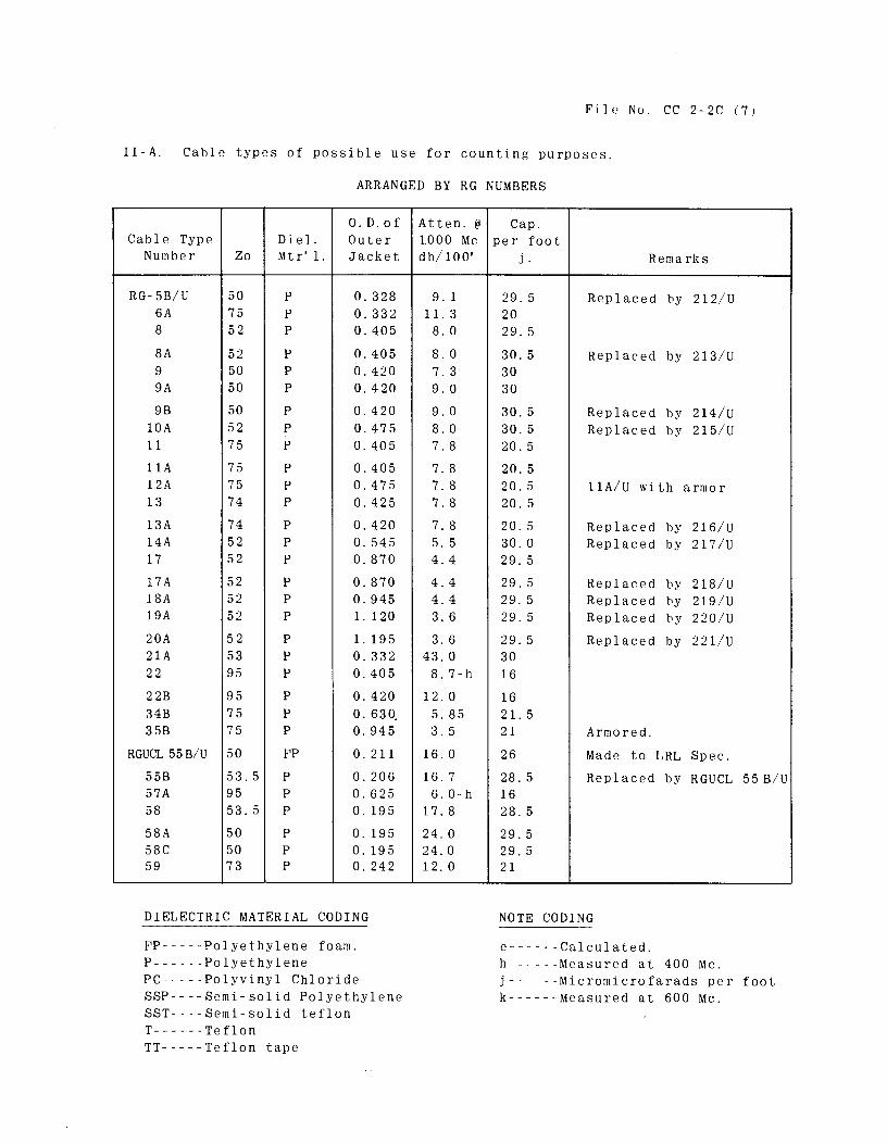
II-A. Cable types of possible use for counting purposes.
ARRANGED BY RG NUMBERS
0. D. of Cable Type Die 1. Outer
Number Zo Mt r' 1. Jacket
RG-5B/U 50 p 0. 328 6A 75 p 0. 332 8 52 p 0.405 SA 52 p 0.405 9 50 p 0.420 9A 50 p 0.420 9B 50 p 0.420
lOA 52 p 0.475 11 75 p 0.405 llA 75 p 0.405 12A 75 p 0.475 13 74 p 0.425 13A 74 p 0.420 14A 52 p 0. 545 17 52 p 0.870 17 A 52 p 0.870 18A 52 p 0.945 J.9A 52 p 1. 120 20A 52 p 1. 19 5 21A 53 p 0. 332 22 95 p 0.405 22B 95 p 0. 420 34B 75 p 0. 630. 35B 75 p 0.945
RGUCL 55B/U 50 FP 0. 211 55B 53.5 p 0. 206 57A 95 p 0.625 58 53. 5 p 0. 195 58A 50 p 0. 195 58C 50 p 0. 19 5 59 73 p 0. 242
DIELECTRIC MATERIAL CODING
FP-----Polyethylene foam. ?------Polyethylene PC-----Polyvinyl Chloride SSP----Semi-solid Polyethylene SST----Semi-solid teflon T------Teflon TT-----Teflon tape
Atten. @ 1000 Mc db/J.00'
9. 1 11. 3 8.0 8.0 7. 3 9.0 9.0 8.0 7.8 7.8 7. 8 7.8 7. 8 5. 5 4.4 4.4 4.4 3.6 3.6
43.0 8. 7-h
12. 0 5. 85 3.5
16.0 16. 7
6. 0- h 1 7. 8 24.0 24.0 12. 0
Cap. per foot
j . Remarks
29. 5 Replaced by 212/U 20 29. 5 30. 5 Replaced by 213/U 30 30 30. 5 Replaced by 214/U 30. 5 Replaced by 215/U 20.5 20. 5 20.5 llA/U with armor 20. 5 20. 5 Replaced by 216/U 30. 0 Replaced by 217/U 29. 5 29. 5 Replaced by 218/U 29. 5 Replaced by 219/U 29. 5 Replaced by 220/U 29. 5 Replaced by 221/U 30 16 16 21. 5 21 Armored. 26 Made to LRL Spec. 28. 5 Replaced by RGUCL 55 B/U 16 28. 5 29.5 29.5 21
NOTE CODING
e------Calculated. h------Measured at 400 Mc. j------Micromicrofarads per foot k------Measured at 600 Mc.
II-A. (Continued)
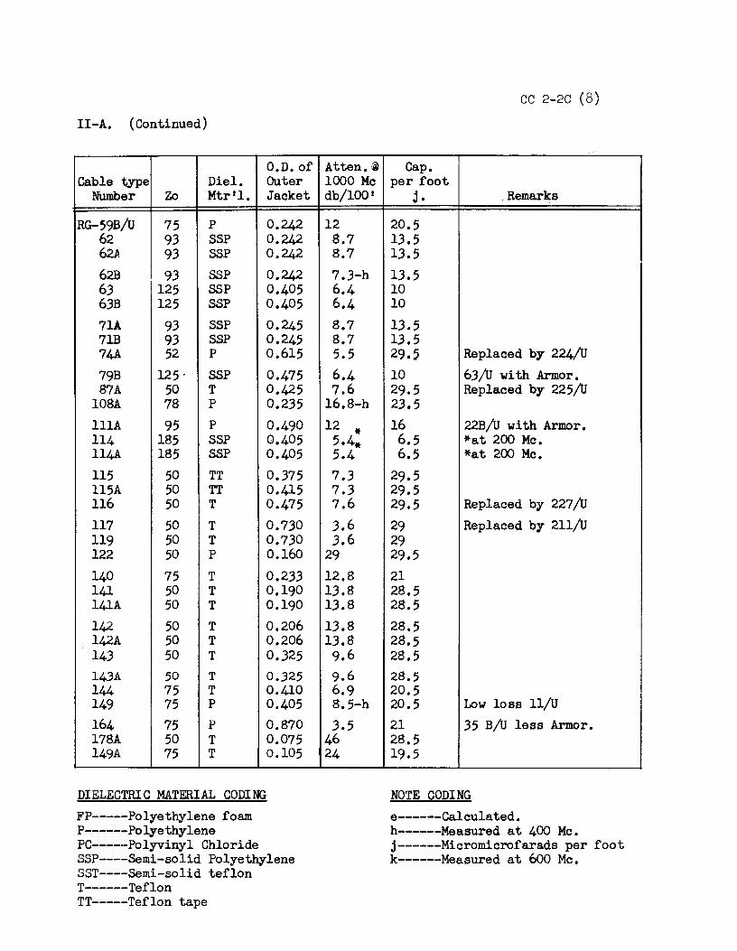
O.D. of Cable t.,ype Diel. Outer
Number Zo Mtr'l. Jacket
RG-59B/U 75 p 0.242 62 93 SSP 0.242 62.A 93 SSP 0.242 62B 93 SSP 0.242 63 125 SSP 0.405 63B 125 SSP 0.405 71A 93 SSP 0.245 71B 93 SSP 0.245 74A 52 p 0.615 79B 125. SSP 0.475 87A 50 T 0.425
108A 78 p 0.235 lllA 95 p 0.490 114 185 SSP 0.405 114A 185 SSP 0.405 115 50 TT 0.375 115A 50 TT 0.415 116 50 T 0.475 117 50 T 0.730 119 50 T 0.730 122 50 p 0.160 140 75 T 0.233 141 50 T 0.190 141A 50 T 0.190 142 50 T 0.206 142A 50 T 0.206 143 50 T 0.325 14JA 50 T O.J25 144 75 T 0.410 149 75 p 0.405 164 75 p 0.870 178A 50 T 0.075 149A 75 T 0.105
DIELECTRIC MATERIAL CODING FP-----Polyethylene foam P------Polyethylene PC-----Polyvinyl Chloride SSP----Semi-solid Polyethylene SST----Semi-solid teflon T------Teflon TT-----Tef lon tape
Atten.@ 1000 Mc db/100 1
12 8.7 8.7 7.3-h 6.4 6.4 8.7 8.7 5.5 6.4 7.6
16.8-h 12 * 5.4* 5.4 7.3 7.3 7.6 3.6 3.6
29 12.8 13.8 13.8 13.8 13.8 9.6 9.6 6.9 8.5-h 3.5
46 24
CC 2-2C (8)
Cap. per foot
j. . Remarks
20.5 13.5 13.5 13.5 10 10 13.5 13.5 29.5 Replaced by 224/U 10 63/U with Armor. 29.5 Replaced by 225/U 23.5 16 22B/U with Armor. 6. 5 *at 200 Mc. 6.5 *at 200 Mc.
29.5 29.5 29.5 Replaced by 227/U 29 Replaced by 211/U 29 29.5 21 28.5 28.5 28.5 28.5 28.5 28.5 20.5 20.5 Low loss 11/U 21 35 B/U less Armor. 28.5 19.5
NOTE CODING e------Calculated. h------Measured at 400 Mc. j------Micromicrofarads per foot k------Measured at 600 Mc.
II-2. (Continued)
0. D. of Cable type Di el. Outer
Number Zo Mtr' 1. Jacket
RG-180 93 T 0. 141 180A 95 T 0. 145 187 75 T 0. 110 188 50 T 0. 110 195 95 T o. 155 196 50 T 0.080 209 50 SST 0.750 210 95 SST 0. 242 211 50 T 0. 730 212 50 p 0. 332 213 50 p 0.405 214 50 p 0. 425 215 50 p 0.475 216 75 p 0. 425 217 50 p 0. 545 218 50 p 0.870 219 50 p 0.945 220 50 p 1. 120 221 50 p 1. 19 5 222 50 p 0. 332 223 50 p 0. 216
225 50 T 0.430 226 50 TT 0. 500 227 50 T 0. 490
K-113 35 FP 0. 195 60-3905 30 PC 0.045
YK 198 16 p 0.566
DIELECTRIC MATERIAL CODING
FP-----Polyethylene foam P------Polyethylene PC-----Polyvinyl Chloride SSP----Semi-solid Polyethylene SST----Semi-solid teflon T------Teflon TT-----Teflon tape
Atten. @
1000 Mc db/100'
17 17 24
31 17 46
2. 5-h 7.0-h 3. 6 9. 1 8.0 9.0 8.0 7.8 5.5 4.4 4.4 3.6 3. 6
43.0 16. 7
7. 6 3. 5-h 7. 6
12-h
13. 2
File No. CC-2-2C (9)
Cap. per foot
j . Remarks
15 15 19. 5 29 15 28. 5 26. 5 13. 5 Formerly 62C/U 29 Formerly 117/U 29. 5 Formerly 5B/U 29. 5 Formerly 8A/U 29. 5 Formerly 9B/U 29. 5 Formerly lOA/U 20. 5 Formerly 13A/U 29.5 Formerly 14A/U 29. 5 Formerly 17A/U 29. 5 Formerly 18A/U 29. 5 Formerly 19A/U 29. 5 Formerly 20A/U 29 Formerly 2 lA/U 29.5 Formerly 55A/U 29. 5 Formerly 87A/U 29. 5 Formerly 94A/U 29.5 Formerly 116/U 39 65
103 Mfr: Belden
NOTE CODING
e------Calculated. h------Measured at 400 Mc. j------Micromicrofarads per foot k------Measured at 600 Mc.

CC 2-2C (10)
II-B. Cable types of possible use for counting purposes.
MINIATURE TYPES (Those with o.d. less than or equal to 0.190 inches.l
CABLE TYPE NUMBER MFR.
RG-122/U RG-141/U RG-141A/U RG-174/U RG-178A/U RG-179A/U RG-180/U RG-180A/U RG-187/U RG-188/U RG-195/U RG-196/U
21-597 Amp. 60-3905 M.
MANUFACTURER CODING Amp. ------Amphenol M.---------Microdot
Zo
50 50 50 50 50 75 93 95 75 50 95 50 75 30
DIELECTRIC MATERIAL CODING P----------Polyethylene T----------Tef lon
Diel. Mtr 11.
p T T p T T
T T T T T T p T
NOTE CODING h----------Measured at 400 Mc.
O.D. of Atten.@ Cap. Outer 1000 Mc per foot Jacket db/100 1 j.
0.160 29 29.5 0.190 14 28.5 0.190 14 28.5 0.100 18-h 29.5 0.075 46 28.5 0.105 24 19.5 0.141 17 15.5 0.145 17 15 0.110 24 19.5 0.110 31 29 0.155 17 15 0.080 46 28.5 0.150 12-h 20 0.045 65
j----------Capacity is in ndoromicrofarad per foot.
REMARKS
CC 2-2C (11)
II-C. Cables types of possible use for counting purposes.
RIGID AND SEMI-RIGID CABLE TYPES
Cable Type Number Mfr. Zo
21-592 Amp. 50 21-606 Amp. 50 21-607 Amp. 75 421-608 Amp. 50 421-609 Amp. 75 FH4 An. 50
FHJ4 An. 50
FH5 An. 50
FHJ5 An. 50
RG-268/U H3-50 An. 50
RG-269/U H5-50 An. 50
RG-285/U H5-100 An. 100
RG-270/U H7-50 An. 50
H7-100 An. 100
-- Prod 125 Styroflex P-D 50 Styroflex P-D 50 Styrofoam UCRL 125 Styrofoam UCRL 125
DIELECTRIC MATERIAL CODING FP-----Polyethylene foam. P------Polyethylene. PT-----Polyethylene tubes. SF-----Styrofoam SP-----Polyethylene spiral. ST-----Teflon spiral T------Teflon TPS----Polystyrene
NOTE CODING
Diel. Mtr'l.
p p p
T T FP
FP
FP
FP
SP
SP
ST
SP
SP
PT TPS TPS SF SF
e------Calculated j------Micromicrofarads per foot
O. D. of Outer Jacket
0.325 0.325 0.325 0.325 0.325 0.540
0.660
0.980
1.100
0.500
1.005
1.005
1.830
1.830
0.875 0.875 3.125 1.500 2.000
Atten.@ Cap. 1000 Mc per foot db/100 1 j. Remarks
7.6 29.5 8/U with solid Cu Shield. 7.6 29.5 8/U with solid Al shield. 7.5 11/U with solid Al shield. 6.2 87A/U with solid Al shield. 6.0 144/U with solid Al shield. 3.33 Corrugated solid CU shield.
Minimum radius 5 ". 3.33 Corrugated solid Cu shield.
Minimum radius 5 ". 2.00 Corrugated solid CU shield.
Minimum radius 10 11 •
2.00 Corrugated solid Cu shield. Minimum radius 10 "·
5.00 Corrugated solid Cu shield. Minimum radius 5 ".
1.07 Corrugated solid CU shield. Minimum radius 10 "·
1.07 Corrugated solid CU shield. Minimum radius 10 11 •
0.79 Corrugated solid Cu shield. Minimum radius 20 11 •
0.79 Corrugated solid Cu shield. Minimum radius 20 1'.
1.4-e 9 Solid Al shield. 1.6 22 Minim.um radius 10 11 •
0.5 22 Minimum radius 50 11 •
0.8 UCRL Spec. (3597). 0.6 UCRL Spec. (3597).
MANUFACTURERS CODI:OO Amp----Amphenol-Borg Electronics Corp. An-----Andrew Corp. P-D----Phelps-Dodge Electronics Products Corp. PROD---Prodelin Inc. UCRL---u.c. Radiation Laboratory Specs.
INNER & OUTER CONDUCTOR CODING Al-----Aluminum Cu-----Copper
CC 2-2C (12)
II-D. Cable types of possible use for counting purposes.
1. DELAY CABLES
Band- D.C. Inner Loss Min. Zo Delay width ohms O.D. Cond. Insert. Max. Radius
Cable Type Number Mfr. ± 10% a. b. ft. inch AWG c. volts inches
RG-266/U alil500A CTC 1500 0.08 15 JO 0.40 29 0.20 5000 2 WU600 CTC 1700 1.0 6 80 0.28 JS 0.40 JOO J
RG-176/U HH2000 CTC 2400 0.11 15 70 0.40 32 0.25 5000 2 HH2500 CTC 3000 0.60 s 125 0.28 JS O.JO 500 J
HH4000 CTC 3900 1.0 6 85 0.32 J8 0.20 1000 4
65A Royal 950 0.04J 0.415 J2 JOOO
a) Microsecond per foot, plus or minus 10%. b) Band-width at one microsecond delay. c) db loss per microsecond delay.
MANUFACTURER CODI NG
CTC) Columbia Technical Corporation. Royal) Inter. Tele. & Tele. Royal

III. PROPERTIES OF DIELECTRICS USED IN COAXIAL CABLES
Dielectric constant at 108 cps
Dissipation factor at 108 cps
Polyethylene
2.25
L0.0005
Temperature variation of -0.0007d dielectric constant per 0 c {at constant pres sure of 1 atmos. )
Dielectric strength, short-time 460a 1/8" thickness, volts/mil Volume resistivity, ohm-cm, 50% humidity, 2 3 °c Refractive index, nd
Coefficient of linear thebmal expansion, parts per 10 / 0 c
1.5 la
160-180a
Mechanical distortion temp., 0 c 41-50a
Brittleness temperature, 0 c -70
Effect of sunlight
Effect of dielectric on metal inserts
Specific gravity
Moisture absorption, 24-hr immersion, 1/8" thick., %
surface crazing-a
inert
0.92a
L.0.015a
Teflon (polytetra-
fluoroethylene)
2.0b
L0.0003b
-0.0003c
480a
,.
L35a
100
J135g l @66 psi -76
none-a
inert
2.l-2.3a
0.005a
Polystyrene
2.4 - 2.65a
0.0001-0.0004a @ 106 cps
-0.0005d
500-700a
1. 59-1.60a
60-80a
70-lOOa
yellows slightly-a
1.04-1.065a
0.03-0.05a
Styrofoam 22 (foamed poly-styrene}
1.025
70f
80f
yellows-£
Air
1.00059e
1.00029e
0.021-0.027£
0.20 lb H 20/ft2
surface area in a week
References: - a) Modern Plastics Encyclopedia, 1955; b) DuPont specs; c) National Bureau of Standards Journal of Research, vol 51, p. 185; d) Calculated; e) Chem. Rubber Hdbk.; f) Dow Chem. Co. specs.; g) Ethylene Chem. Corp.
0 0 [\) I
[\) 0

CC 2-2C (14)
IV. Temperature coefficient of length of certain cables.
RG 8, 63, 87A. The temperature coefficient of electrical length is a function of temperature, but near room temperatures, the coefficient is essentially a constant. Measured values are tabulated below.
Cable type
RG 8 63 87A
0 *Not measured below + 20 C.
Temp. coeff.
-2x10- 4 - 1x10- 4 - 1x10- 4
In temp. range
+ 20° to + so 0 c* - 20° to + so 0 c - 60° to + so 0 c
A 100 foot length of RG 63 will therefore change its electrical length about 0.012 millimicroseconds per degree antigrade.
UCRL Styrofoam: Measurements showed the temperature coefficient to be within ± 2 X 10⁻⁵ ~arts per 0 c. (The linear expansion of the copper conductors is + 2X 10- parts per 0 c).
V. Noise
"Internal noise" - Owing to manufacturing tolerancea the characteristic impedance of a coaxial cable varies along its length. When a pulse travels along the line, reflections are generated by the changing impedance levels. The signal at the output, then, consists of the original pulse followed by a series of smaller, internally generated pulses, the latter referred to as _ 10 "internal noise." When a pulse from a mercury pulse of risetime -< SX 10 is transmitted along a cable such as RG8 or RG 63, the amplitude of the in-ternal-noise pulses observed is of the order of 1% of the amplitude of the initial pulse, when the observing instrument has a risetime of ,,._ 10-9 seconds (517' scope-direct connections to deflecting plates). Cables having closer mechanical tolerances (e. i. Styroflex) exhibit internal noise of smaller am-plitude relative to the signal pulse.
VI.
0 ~
CC 2-2C ( 15)
10-81.-~~~~~~~~~1--~~~~~~~~~1-r-~~-r~~~t--~~1
8
I I I I __J_ ~~.~1-a-h-7-1-0-o~r-t~~...__~~...__1~.~o~~....._~~..._~~---1~0..--~--'-~~__..~- so
@400 MC
a. - - A TTENU AT ION AT IN DIC A TED FREQUENCIES {db/100 feet)
RISE TIME CONVERSION FACTORS
For pulses of the shape shown in Fig. 5 of CC2-l, the rise times from 0 to x% can be expressed as multiples of T , where T
0 is the 0 to 50% rise
time:- Pulses of this shape are generated $hen step-function waveforms are applied to th/ inputs of transmission lines for which attenuation varies as (frequency) 1 2 • (See CC2-l)
~ 0 to ~rise time To
10 0.17 20 0.28 50 1.0 70 3.1 80 7.3 90 29 95 110
The 10 to 90% rise time is thus (29 - 0.17) T0
~ 28.83 T0
;
CC 2-2C (16)
.3
I/I a:: .2 .... INNER CONOUCTOR "' 0 .... 0
DIELECTRIC ;300 "' ... 2 2
~ 6 s a:: 2 Q "' ;;) 0 IL ;;) ... I 200 ~ u 4 "' >-z j a:: :I:
0 "' u g ... ~
IL 6 z I e c Q - Q ~ "' ::a. 8 "' .10 u f ::a. 10 ~ 100 u z o= 1.00 I";" ... j! IE • ¥ 80 0 4 u .90 "' u .... u t:= 0 .08 ;;)
~e .... z 20 60 fi Q
.80 z c I/I ~ >- ::i
2i .... ii: a:: u "' 3 I ....... . 70 f .... I ..J -o u 40
9~ 0 ~
40 c ~ .06 u a:: .60 30 ~ Q
~c:; I 60 30 ..,o ii: u 80 > iil .... I
~ 0 -> N 2 ~- ...I .04 ...I "' "' iS a:: I I ¥ CQ,
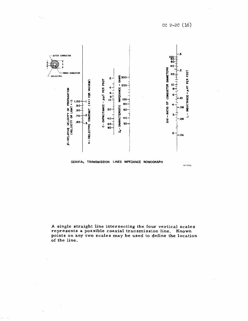
COAXIAL TRANSMISSION LINES IMPEDANCE NOMOGRAPH MU-12192
A single straight line intersecting the four vertical scales represents a possible coaxial transmission line. Known points on any two scales may be used to define the location of the line.
CC 2-2C (17)
VIII. Transmission line formulas
1. Z - characteristic impedance of coaxial lines with perfectly conducting cgnductors
=P. D d ohms
For dielectrics for which µ. = µ. 0 (this includes the commonly used dielectrics)
where
= 377 .ln J2. 2rr,/K E d = ~ .tn -1L ./K E d
138 .lL = ,fK loglO d
µ. = permeability of dielectric - henriaf'meter
....,0
E
= permeability of vacuum
:' 4'1t' x 10- 7 henry/meter
= permittivity of dielectric - farads/meter E
0 = permittivity of vacuum
"t 3 ~'1t' x 10- 9 farads/meter K = dielectric constant
E = Eo D = inside diameter of outer conductor d = outside diameter of inner conductor
The impedance of a transmission line having distributed inductance (L - henries per unit length) and distributed capacitance (C - farads per unit length) is, neglecting the effects of conductor resistance,
z = Ck 0 "'c
2. v - Velocity of propagation of transmission-line waves (TEM mode)
1 v = f7i7 meters/second 'V J.LE
where µ., E are respectively the permeability and permittivity of the dielectric. For dielectrics for which µ. = µ. ,
0
v = B':c
3xl0 K meters/second
f3 = L = _l_ c -.JK
c = velocity of propagation in vacuum.
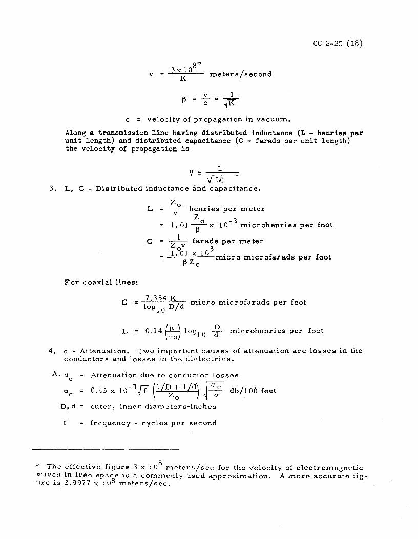
CC 2-2C (18)
Along a transmission line having distributed inductance (L - henries per unit length) and distributed capacitance (C - farads per unit length) the velocity of propagation is
1 v = -----v LC 3. L, C - Distributed inductance and capacitance.
L = =
c = =
For coaxial lines:
Zo -- henries per meter
v z 1. 01 Tx 10- 3 microhenries per foot
-z;-1-- farads per meter ov 3
1.01x10 . . f d f t f3 Zo micro micro ara s per oo
c = 7 ·· 354 K micro microfarads per foot log 10 D/d
L = 0.14(~10)1og 10 ~ rnicrohenriesper foot
4, a - Attenuation. Two important ca.uses of attenuation are losses in the conductors and losses in the dielectrics.
A. a. - Attenuation due to conductor losses c (7. = 0.43 x 10 -3 ./f (l/D + l/dj ~ a c db/l 00 feet c· Z 0 a
D, d = outer 0 inner diameters-inches
f = frequency - cycles per second
':' The effective figure 3 x 10⁸ meters/sec for the velocity of electromagnetic w,1vcs in fr ec eipace. is a commonly •.u;cd a.pproximation. A . .norc accurate fig-ure is 2.9977 x 10⁸ meters/sec.
CC 2-2C (19)
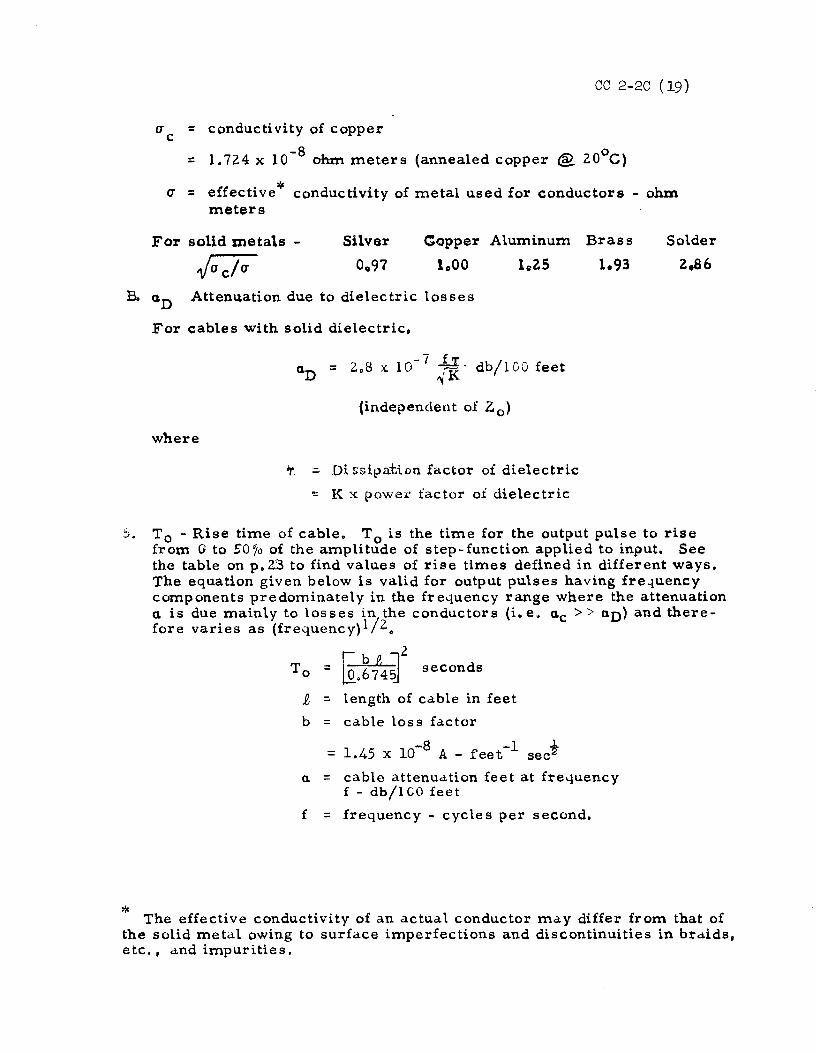
u = conductivity of copper c = 1. 724 x 10-S ohm mete-rs (annealed copper @. 20°C)
u = effective* conductivity of metal used for conductors - ohm meters
For solid metals - Silver
Oa97 Copper Aluminum
Jac/u i.oo i~is
B. a.D Attenuation due to dielectric losses
For cables with solid dielectric,
where
- 1 f... I a.D = 2..8 x 10 {R-· db 100 feet
(independent of Z 0 )
'r =- Di ssi.pati.on factor of dielectric
'!:: K x powei· factor oi dielectric
Brass
1.93 Solder
z.a6
S. T 0 - Rise time of cable. T 0 is the time for the output pulse to rise from 0 to 50~o of the amplitude of step-function applied to input. See the table on p. 23 to find values of rise times defined in different ways. The equation given below is valid for output pulses having fre-iuency components predominately in the freyuency range where the attenuation a. is due mainly to losses in/the conductors (i.e. a.c >> a.n) and there-fore varies as (frequency)! z..
To = lli b g ~2 .6745 seconds
p, = length of cable in feet b = cable loss factor
= -8 -1 t 1.45 x 10 A - feet sec Q = cable attenuation feet at frequency
f - db/1 CO feet f = frequency - cycles per second.
The effective conductivity of an actual conductor may differ from that of the solid metal owing to surface imperfections and discontinuities in braids, etc., and impurities.
File No. CC 2-6B (1) c. N. Winningstad Rev. May 28, 1964 L. Wagner
Lawrence Radiation Laboratory, University of California, Berkeley
COUNTING NOTE
NANOSECOND - PULSE TRANSFORMERS, ATTENUATORS, AND TERMINATORS
I. ABSTRACT The combination of high-frequency response and good sensitivity
inherent in most nuclear instrumentation equipment gives rise to the need for close attention to impedance matching between various units and to terminating coaxial cables. The variety of impedance discon-tinuities encountered can usually be eliminated by the use of pulse transformsers, attenuators, and/or terminators. The type of matching most appropriate in a given circumstance will depend upon considerations and possibly compromises involving relative energy transfer, range of frequencies involved and available signal levels.
This note describes a variety of pulse transformers, terminators, and attenuators in use at LRL, Berkeley.
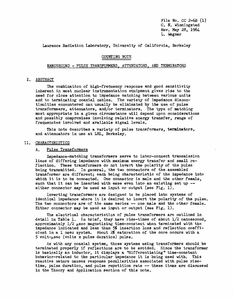
II. CHARACTERISTICS A. Pulse Transformers
Impedance-matching transformers serve to inter-connect transmission lines of differing impedance with maximum energy transfer and small re-flection. These transformers do not invert the polarity of the pulse being transmitted. In general, the two connectors of the assembled transformer are different; each being characteristic of the impedance into which it is to be connected. One connector is male and the other female, such that it can be inserted with ease even into an existing set up --either connector may be used as input or output (see Fig. 1).
Inverting transformers are designed to be placed into systems of identical impedance where it is desired to invert the polarity of the pulse. The two connectors are of the same series -- one male and the other female. Either connector may be used as input or output (see Fig. 1).
The electrical characteristics of pulse transformers are outlined in detail in Table 1. In brief, they have rise-times of about 1/2 nanosecond, approximately 1/2 µsec magnetizing time-constant when terminated with the impedance indicated and less than 5% insertion loss and reflection coeffi-cient in a 1 nsec system. About 2% saturation of the core occurs with a 5 volt-µsec (volts x pulse duration) pulse.
As with any coaxial system, those systems using transformers should be terminated properly if reflections are to be avoided. Since the transformer is basically an inductor, it displays a ''differentiating" time-constant behavior-related to the particular impedance it is being used with. This reactive nature causes response peculiarities associated with pulse rise-time, pulse duration, and pulse repetition rate -- these items are discussed in the Theory and Application section of this note.
CC 2-6B (2}
B. Uni-direction and Bi-direction Matching Units These are impedance-matching resistive networks that properly termin-
ate a coaxial line of one impedance when coupled through the matching unit to a line of a different impedance. By means of the matching unit, reflec-tions at the junction of the two impedances are reduced to low values.
Two types of matching units are made, uni-directional matching units (UDM), which provide an impedance match at only one connector, and bi-direc-tional matching units (BDM), which provide an impedance match at both connectors.
The disadvantage of matching units over transformers is that a power loss or attenuation is incurred. The advantage is that the response is constant down to zero frequency. The amount of attenuation is listed in its reciprocal form as voltage transmission coefficient in Table II. In general, the UDM units have lower attenuation than the BDM.
Capacitive or inductive reflection components are less than 2% of the original signal in a 1 nsec rise-time system. The maximum resistive reflection coefficient which arises because of the 5% tolerances of the resistors is listed in Table II.
1. Uni-direction Matched (UDM): Uni-directional matched units pro-vide a low-reflection impedance match at only one of its two connectors when used as recommended. As an example, when a 125-ohm cable is connected to connector 2 of UDMlA, its 125-ohm impedance in parallel with the 82-ohm resistor Rl, provides a 50-ohm input impedance at connector 1, thereby matching a 50-ohm cable. However, with a 50-ohm cable connected to connector 1, the input impedance at connector 2 is 50-ohms paralleled with 82-ohms, or 31-ohms, which does not match the 125-ohm cable. Thus, the uni-directional matched series is primarily designed to be used with signals traveling into connector 1 and out of connector 2 (left to right as the diagram is shown - accompanying Table II).
2. Bi-directional Matched (BDM): Bi-directional units provide a low-reflection impedance match at both of its connectors when cables of impedances z1 and z2 are connected respectively to connectors 1 and 2.
c. Non-matched Adapters (NM) These provide convenient me'ins of connecting coaxial cables having
different types of connectors. If the two cables are not of the same im-pedance, reflections will occur at the adapter and the voltage transmission coefficient will be other than unity. The transmission and reflection coefficients for various combinations of impedances z1 and z2 are listed in Table IV. D. Attenuators
These may be inserted into coaxial lines of the specified lmpedance to attenuate pulses. At either connector an impedance match to within 2$ is provided for lines of the specified impedance. The same attenuation is obtained for signals traveling in either direction. E. Terminators
These units contain one or more resistors to properly terminate coaxial transmission lines of the specified impedance z. Capacitive or inductive reflections from the terminators are held to less than 2$ in a 1 nsec rise-time system. Resistor values are held to within 2$ of the figures quoted, therefore the resistive reflection coefficient is less than 1%.
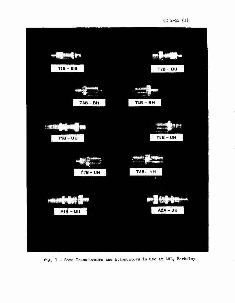
CC 2-6B (J)
Fig. 1 - Some Transformers and Attenuators in use at LRL, Berkeley
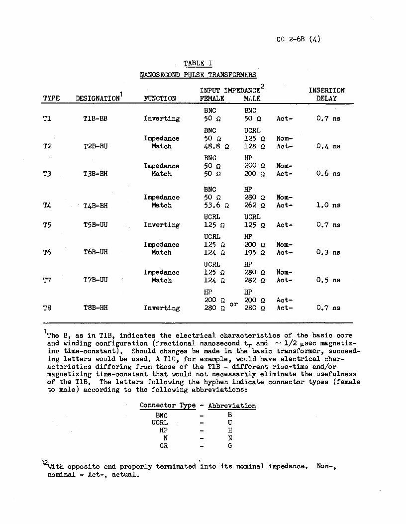
CC 2-6B (4)
TABLE I NANOSECOND P!.!LSE TRANSFORMERS
DESIGNATION 1 INPUT IMPEDANCE2 INSERTION TYPE FUNCTION FEMALE MALE DELAY
BNC BNC Tl TlB-BB Inverting 50 Q 50 Q Act- 0.7 ns
BNC UCRL Impedance 50 Q 125 Q Nom-
T2 T2B-BU Match 48.8 Q 128 Q Act- 0.4 ns BNC HP
Impedance 50 Q 200 Q Nom-TJ TJB-BH Match 50 Q 200 Q Act- 0.6 ns
BNC HP Impedance 50 Q 280 Q Nom-
T4 T4B-BH Match 53.6 Q 262 Q Act- 1.0 ns UCRL UCRL
T5 T5B-UU Inverting 125 Q 125 Q Act- 0.7 ns UCRL HP
Impedance 125 Q 200 Q Nom-T6 T6B-UH Match 124 Q 195 Q Act- O.J ns
UCRL HP Impedance 125 Q 280 Q Nom-
T7 T7B-UU Match 124 Q 282 Q Act- 0.5 ns HP HP 200 Q 200 Q Act-
T8 T8B-HH Inverting 280 Q or 280 Q Act- 0.7 ns
1The B, as in TlB, indicates the electrical characteristics of the basic core and winding configuration (fractional nanosecond tr and ~ 1/2 µsec ma.gnetiz-in~ time-constant). Should changes be made in the basic transformer, succeed-ing letters would be used. A TlC, for example, would have electrical char-acteristics differing from those of the TlB - different rise-time and/or magnetizing time-constant that would not necessarily eliminate the usefulness of the TlB. The letters following the hyphen indicate connector types {female to male) according to the following abbreviations:
Connector Type -BNC
UCRL HP
N GR
Abbreviation B u H N G
12with opposite end properly terminated into its nominal impedance. Non-, nominal - Act-, actual.
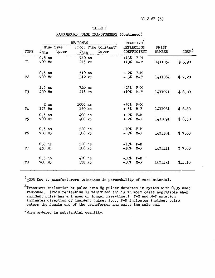
CC 2-6B (5)
TABLE I NANOSECOND PULSE TRANSFORMERS (Continued)
RESPONSE Constant3 REACTiw4
Rise Time Droop Time REFLECTION PRINT TYPE fJdb Upper fJdb Lower COEFFICIENT NUMBER cosT5
0.5 ns 740 ns +13% F-M Tl 700 Mc 215 kc +13% M-F 14Xl051 $ 6.80
0.5 ns 510 ns - 21, F-M T2 700 Mc 312 kc - 3% M-F 14Xl061 $ 7.20
1.5 ns 740 ns -25% F-M T3 230 Mc 215 kc +10% M-F 14Xl071 $ 6.80
2 ns 1000 ns +30% F-M T4 175 Mc 159 kc + 5% M-F 14X1081 $ 6.80
0.5 ns 400 ns + 21, F-M T5 700 Mc 400 kc + 2$, M-F 14X1091 $ 6.50
0.5 ns 520 ns -10% F-M T6 700 Mc 306 kc - 8% M-F 14Xll01 $ 7.60
o.8 ns 520 ns -15% F-M T7 440 Mc 306 kc -10% M-F 14Xllll $ 7.60
0.5 ns 410 ns -30% F-M T8 700 Mc 388 kc -30% M-F 14Xl121 $11.10
3±20% Due to manufacturers tolerance in permeability of core material. 4Transient reflection of pulse from Hg pulser detected in system with 0.35 nsec
response. (This reflection is minimized and is in most cases negligible when incident pulse has a 1 nsec or longer rise-time.) F-M and M-F notation indicates direction of incident pulse; i.e., F-M indicates incident pulse enters the female end of the transformer and exits the male end.
5When ordered in substantial quantity.
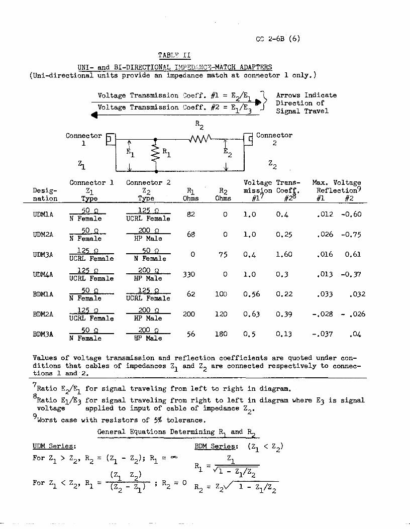
CC 2-6B (6)
TABLr: II UNI- and BI-DIRECTIONAL IMPEDM~CE-MATCH ADAPTF,RS
(Uni-directional units provide an impedance match at connector 1 only.)
Voltage Transmission C:oeff. #1 = E2/E1 } Arrows Indicate Voltage Transmission Coeff'. - . Direction of #2 - E1/E3 Signal Travel
~ R2
Conn~ctor ~;l ~-. Connector !Rl 2
2 21 l z2
Connector 1 Connector 2 Voltage Trans- Max. Voltage Ref'lection9 Desi.g- Z1 Z2 R1 R2 mission Coeff.
nation Type Type Ohms Ohms #17 #28 #1 #2
UDMlA ~o ~ 122 Q 82 0 1.0 0.4 .012 -0.60 N Female UCRL Female
UDM2A 20 ~ 200 ~ 68 0 1.0 0.25 .026 -0.75 N Female HP Male
UDM3A 122 ~ ~o £2 0 75 0.4 1.60 .016 0.61 UCRL Female N Female
UDM4A 122 ~ 200 ~ 330 0 1.0 0.3 .013 -0.37 UCRL Female HP Male
BDMlA 20 ~ 122 ~ 62 100 0.56 0.22 .033 .032 N Female UCRL Female
BDM2A 122 ~ 200 Q 200 120 o.63 0.39 -.028 - .026 UCRL Female HP Male
BDM3A 20 ~ 200 ~ 56 180 0.5 0.13 -.037 .04 N Female HP Male
Values of' voltage transmission and ref'lection coef'f'icients are quoted under con-ditions that cables of impedances z1 and z2 are connected respectively to connec-tions 1 and 2.
7Ratio E2/E1 for signal traveling from left to right in diagram. 8Ratio E1/E3 f'or signal traveling f'rom right to lef't in diagram where EJ is signal voltage applied to input of cable of' impedance z2•
9worst case with resistors of 5% tolerance.
UDM Series:
General Equations Determining R1 and R2
(Zl - Z2); Rl = oc:.
(Zl Z2) (Z2 - Zl)
BDM Series: (z1 < z2)
Ri = v1 - Z /Z 1 2
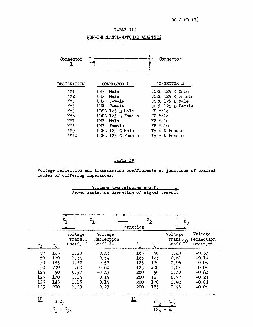
Connector 1
DESIGNATION NMl NM2 NMJ NM4 NM5 NM6 NM7 NM8 NM9 NMlO
CC 2-6B (7)
TABLE III NON-IMPEDANCE-MATCHED ADAPTERS
~I-------~ Connector 2
CONNECTOR 1
UHF Ma.le UHF Ma.le UHF Female UHF Female UCRL 125 Q Male UCRL 125 Q Female UHF Male UHF Female UCRL 125 Q Male UCRL 125 Q Female
TABLE IV
CONNECTOR 2 UCRL 125 Q Male UCRL 125 Q Female UCRL 125 Q Male UCRL 125 Q Female HP Male HP Male HP Male HP Male Type N Female Type N Female
Voltage reflection and transmission coefficients at junctions of coaxial cables of differing impedances.
Voltage transmission coeff. ~ Arrow indicates direction of signal travel.
,. c- qr -- -------;.rT E I zl Z2 I E 1 .2
~unction L___o!.. --··
Voltage Voltage Voltage Voltage Trans10 Reflection Trans.10 Reflect{fn
z1 z2 Coeff. Coeff.11 z1 z2 Coeff. Coeff. ·-
50 125 1.43 0.43 185 50 0.43 -0.57 50 170 1.54 0.54 185 125 0.81 -0.19 50 185 1.57 0.57 185 170 0.96 -0.04 50 200 1.60 0.60 185 200 1.04 0.04
125 50 0.57 -0.43 200 50 0.40 -0.60 125 170 1.15 0.15 200 125 0.77 -0.23 125 185 1.15 0.15 200 170 0.92 -0,08 125 200 1.23 0.23 200 185 0.96 -0.04
10 2 z2 11
(Z2 - Zl) (Zl + Z2) (Z2 + zl)
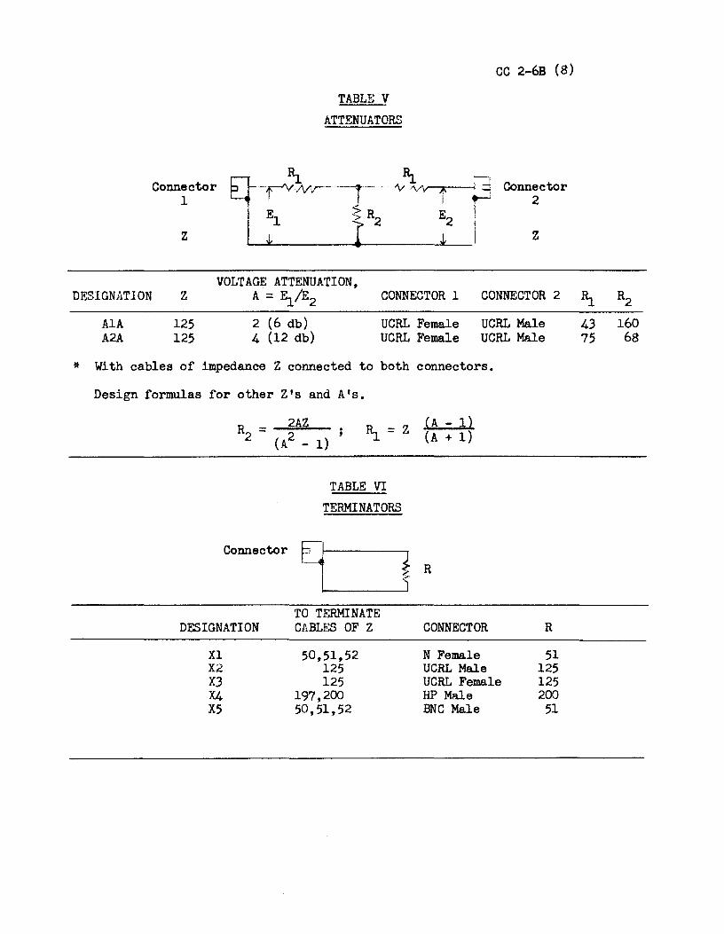
Connector 1
z
TABLE V ATTENUATORS
VOLTAGE ATTENUATION,
CC 2-6B (8)
Connector 2
z
DESIGNATION Z A = E1/E2 CONNECTOR 1 CONNECTOR 2 Hi_ R2 AlA 125 2 (6 db) UCRL Female UCRL Male 43 160 A2A 125 4 (12 db) UCRL Female UCRL Male 75 68
* With cables of impedance Z connected to both connectors.
Design formulas for other Z's and A's.
R _ 2AZ • 2 - (A2 - 1) ,
Connector
TABLE VI
TERMINATORS
TO TERMINATE DESIGNATION CABLES OF Z
Xl 50,51,52 X2 125 XJ 125 X4 197,200 X5 50, 51, 52
(A - 1) (A + 1)
CONNECTOR
N Female UCRL Male UCRL Female HP Male BNC Male
R
51 125 125 200
51
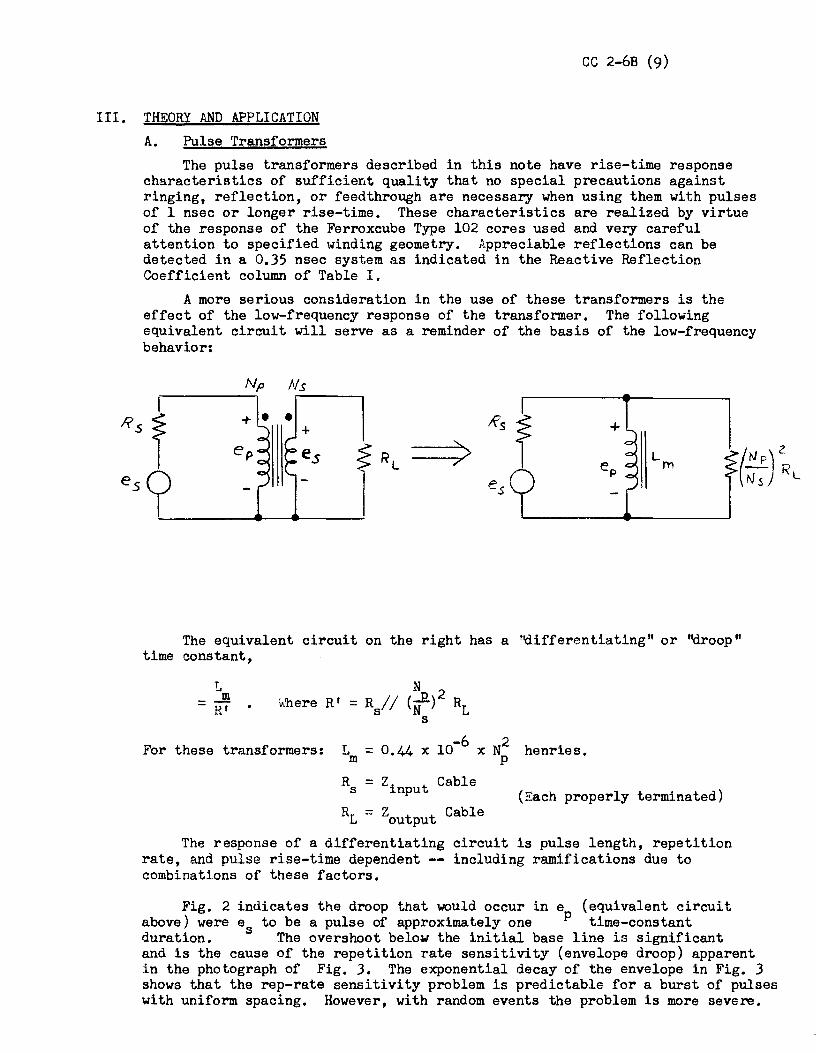
CC 2-6B (9)
III. THEORY AND APPLICATION A. Pulse Transf orrners
The pulse transformers described in this note have rise-time response characteristics of sufficient quality that no special precautions against ringing, reflection, or feedthrough are necessary when using them with pulses of 1 nsec or longer rise-time. These characteristics are realized by virtue of the response of the Ferroxcube Type 102 cores used and very careful attention to specified winding geometry. Appreciable reflections can be detected in a 0.35 nsec system as indicated in the Reactive Reflection Coefficient column of Table I.
A more serious consideration in the use of these transformers is the effect of the low-frequency response of the transformer. The following equivalent circuit will serve as a reminder of the basis of the low-frequency behavior:
Np Ns
Rs f + Rs + ep > (~pr es RL L
eP m Ns RL es e .s
The equivalent circuit on the right has a 'tiifferentiating" or "droop" time constant,
For these transformers: L -6 x N2 henries. = 0.44 x 10 m p R = Zinput Cable s
(~ach properly terminated) RL = Zoutput Cable
The response of a differentiating circuit is pulse length, repetition rate, and pulse rise-time dependent including ramifications due to combinations of these factors.
Fig. 2 indicates the droop that would occur in e (equivalent circuit above) were e to be a pulse of approximately one p time-constant duration. s The overshoot below the initial base line is significant and is the cause of the repetition rate sensitivity (envelope droop) apparent in the photograph of Fig. 3. The exponential decay of the envelope in Fig. 3 shows that the rep-rate sensitivity problem is predictable for a burst of pulses with uniform spacing. However, with random events the problem is more severe.
CC 2-6B (10)
Fig. 4 is a photograph of a single trace which is displaying a gated burst of randomly spaced pulses. Fig. 5 is a multiple trace exposure of the same condition -- it too is predictable, but only on an average basis with random extremes far outside the excursion of the fixed burst rate of Fig. 3. The photograph of Fig. 6 displays a similar circumstance when the pulses are of a considerably narrower width, thereby diminishing the degree of envelope droop.
The multiple exposure photograph of Fig. 7 displays the effect of input pulse rise-time on output pulse peak amplitude. The photograph is comparison of three pairs of input-output comparisons. Each pair has a common initial rate of rise, but the output quickly droops off in each case while the inputs all rise to the 4 om level, each at its own rise-time. Since the same circuit {differentiating time-constant) applies to all three pairs, the varying outputs in the three oases are attributable to the differing rise-times of the inputs. An exponential type rise-time is used for this illustration and for a graph which follows. The output pulse reaches its maximum value before the 9lf%, point on the input pulse, which results in this approximation being independent of the input pulse width, provided the leading edge has the exponential rise characteristic.
Figures 8 and 9 make it possible to determine at a glance if low-frequenoy response problems are likely to be troublesome in a given situation. In order to use these graphs, it is necessary to know only the pulse shapes involved (usually known for p.m. tube bases or eleotroni~ circuits), circuit time constant (Droop Time Constant under Response column in Fig. 1), and an estimate of the average frequency within the burst of the pulse source.
From Fig. 8, the peak output amplitude can be established as a function of the rise-time of the input pulse. From Fig. 9, the possibil-ity of envelope droop as a function of input pulse width and the average frequency within the burst can be determined.
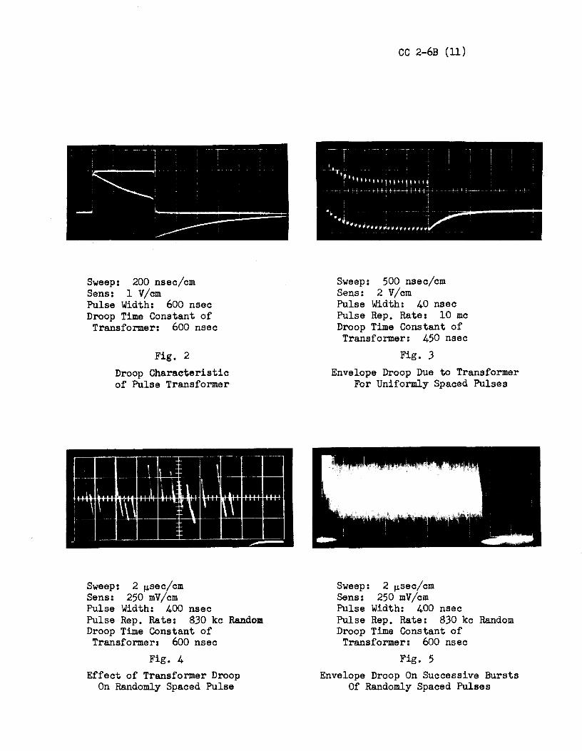
Sweep: 200 nsec/cm Sens: 1 V/cm Pulse Width: 600 nsec Droop Time Constant of Transformer: 600 nsec
Fig. 2 Droop Characteristic of Pulse Transformer
Sweep: 2 µsec/cm Sens: 250 mV/cm Pulse Width: 400 nsec Pulse Rep. Rate: 830 kc Random Droop Time Constant of Transformer: 600 nsec
Fig. 4 Effect of Transformer Droop
On Randomly Spaced Pulse
CC 2-6B (11)
Sweep: 500 nsec/cm Sens: 2 V/cm Pulse Width: 40 nsec Pulse Rep. Rate: 10 me Droop Time Constant of Transformer: 450 nsec
Fig. 3 Envelope Droop Due to Transformer
For Uniformly Spaced Pulses
Sweep: 2 µsec/cm Sens: 250 mV/cm Pulse Width: 400 nsec Pulse Rep. Rate: 830 kc Random Droop Time Constant of
Transformer: 600 nsec Fig. 5
Envelope Droop On Successive Bursts Of Randomly Spaced Pulses
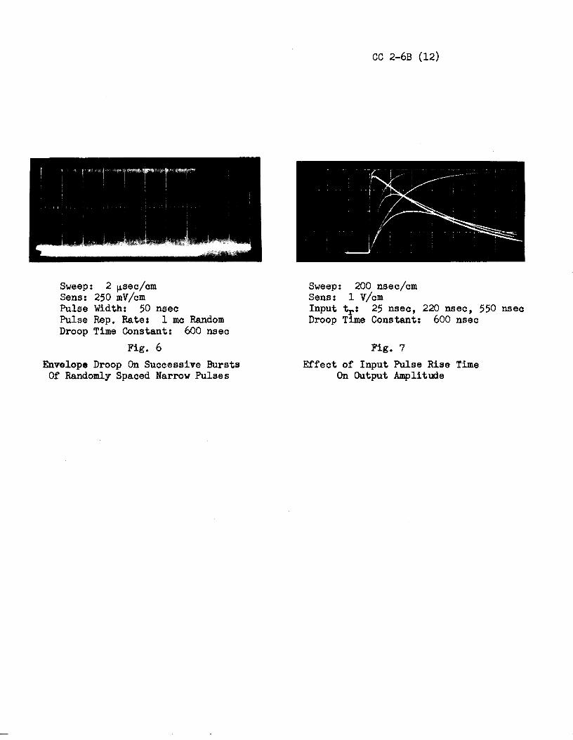
Sweep: 2 µsec/cm Sens: 250 mV/cm Pulse Width: 50 nsec Pulse Rep. Rate: 1 me Random Droop Time Constant: 600 nsec
Fig. 6 Envelope Droop On Successive Bursts
Of Randomly Spaced Narrow Pulses
CC 2-6B (12)
Sweep: 200 nsec/cm Sens: 1 V/cm Input tr: 25 nsec, 220 nsec, 550 nsec Droop Time Constant: 600 nsec
Fig. 7 Effect of Input Pulse Rise Time
On Output Amplitude
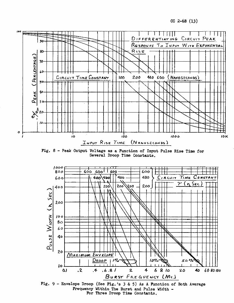
/00
0
CC 2-6B (13)
- I I I I I I I II I I I I I I I ---= --t-- D IF= FE' R ~ N,. ,, ... .,.. ING- c IR c. u IT Pt: AK -- --- -..:::::----_9.; \ ......
~ --....
r----...... r--..... R1;; s PO~ S' E' ........ ;-....... :--.. Io I NP1.17' W 1Tw fxPorH:NTIA&,.. ~ r---. r-.... "'r--,.._
" ~ ..... R•s.i= v- """ ..... r--" ........ f'-..-~~ """--~ !'-...
ll1 10 I'... "' ~
...... I' I'
~~ "" ""' f'-r--..
""" ""' .., ,-v " ' ' .... a:: C1Rcu1T T1Mc C'oNSTAAl"T 100 200 40lJ ~OD ( NAt-it>SH.O•Jl>S) ~ 5- .... '-
"""' ~ ~ "'r--., I'\
~ ...... "" ~ 'lb
'"" I"- I'-, ~ ct w !'-... 0.. 3.
'""' I'" 1 r--.. "!'--~ ~ r--... ~~=
I'..
"'r-.. "" ......... ...., I'-.
<I> ' r--,... !"'-.. ~ I"'--. !"...... r---. ,.._ r-.. I 'o --r-- ~ r-. ~
r--- ,.....
10 IOD 1000
I"' PUT R I~ t: T1 IY'I£. (N AN() s. c C.0"1 bS. )
Fig. 8 - Peak Output Voltage as a Function of Input Pulse Rise Time for Several Droop Time Constants.
~
v II.I \I'
~ .....,,,,
~ 0
~ UJ If\ ..J a:
/000 806
Goo
400
2.00
/00
Bo 60
40
20
I ... 600 .~oo I I 600 600 I I I I I I I I I I I I I I
I I I I I I I I I I I I I
\ 40_~ ~l>l{) ttoo > (I RC.LJl'"T Ti NII: C 0 NS"TAAI T 4{)() '\'
2.ooJ y ( t'\.. Si:<-) \ ' 2.o'~ 2o~oo _ \ \.' \ \ ~
\ ' \\ I~ \ \\ l\. \ \\ \~ ~
~ \ 0-' ' ' \ ' '\ ~
\ \ \. \. '\ "~
' ' \ '\.\. \ ''-' \ \ ~ \ "~
\ ~ \ ~ I\ \ \ '"'\ \ ~ .\. I'\
'~\ \ ~ \ ~
' ~ \ MA'l..llf)IJk1 fNV£LoP~ \ \ \ ~~'.\ ~
I I 0RooP I '61~ ~ \. -y lb'7 ... -~ so~~ I 1 I I II ~ \ I I I I 1 I I I
r-.;:::: ..........
IOK
lo 0.1 • 2. .4 • I:. .B I 2. 4 6 g /{J 40 UJ i() /(JO
BuR.':)Y' Fl\.EGIJE:WC.'1 (McJ Fig. 9 - Envelope Droop {See Fig. 's 3 & 5) As A Function of Both Average
:Frequency Within The Burst and Pulse Width -For Three Droop Time Constants.

CC 2-6B {14)
B. Signal Transmission
Fig. 10 summarizes the signal transmission characteristics specified in the earlier tables. Since the various other coupling methods {Direct, UDM and BDM of Fig. 10) do not have low-frequency response problems, they may sometimes be preferred to the transformer for coupling between systems of differing impedance. Notably, the straight-through method usually gives close to the same transmitted signal as the transformer -- however, it usually results in a large reflection which must be back-terminated to avoid multiple pulsing. The specific circumstances will allow one to decide which method of coupling to use.
c. Attenuators
When the load impedance driven by AlA and A2A attenuators is some-thing other than the intended 125 ohms, the attenuation likewise varies from the intended 2:1 and 4:1. For the usual case where a slight mis-match is encountered, a -2/l relationship {% impedance mis-match/% deviation in attenuation) exists.
A +2% impedance mis-match thereby results in a -1% deviation in attenuation. This relationship is practical {within a percent) for impedance mis-matches up to 10%.
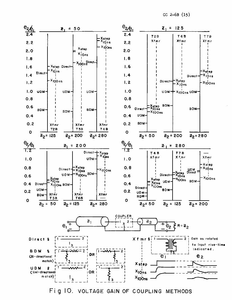
e~, 2.4
2.2
2.0
1.8
1.6
1.4
1.2
1.0 0.8
0.6
0.4
0.2
0
~I 1.2
1.0
0.8
0.6
0.4 0.2
0
Direct
VDM
BDM
Direct
UD"M
BDM
~ :: 5 0
Xstep Direct Xidns
I
I I
X100 ns I
I
Xfmr T2B
UDM
BDM
Xstep
Xians I I 0' X1oons trect I I I I I I I I UDM I I I : SOM I I I
Xfmr T3B
~2= 200
ti = 20 0
Direct
UDM ~step
1qns Xroons BDM
' I xtrrir T3B
Direct
UDM
Xstep x1ons XIOonsBDM
I Xfmr T6B
~st,ep IQns
x1dons I I I
I I
I Xfmr T4B
~Stj'p IOcis
I
I I I
X19ons I I I I I I
Xfmr
~ = 50 ~=125 ~2= 280
e~ --1 2.4
2.2
2.0
1.8
1.6
1.4 I. 2
1.0 0.8
0.6
0.4
0.2
0
~~I T.2
1.0
0.8
0.6
0.4 0.2
0
COUPLER
Direct
UDM
BDM
Direct UOM BOM
CC 2-6B (15)
l1 = 12 5
128 T 6 'B Xf m r >tf mr
I I I I I
I I
Direct I Direct Xstep
X16ns I I
UDM. Xtoons UDM
I Xxstep BDM
IOns X1oons
~2 = 200
ti= 280
BDM
T4B T7B Xf mr
'
: Direct Xstep Xrons UDM X1oons
BDM
X f,mr I I I I UDM
~tep Direct IOns
><icons BDM
T7B Xf mr
I I I I I I I I
Xstep X1ons
' I X1oons
Xfmr I 1
Xst,ep X1ons
' I I
X1oons
~2= 50 ~ = 125 ~2= 200
e~ [ j i-, r-,-:234{ ~2 ) +9R=~2 L- -t--' = I '- I
r---------i Direct' 1 1 2 1
I I I L----~---.J
BDM \ l-,------2; lj-------2~
CBl-dtrectional I ~ I OR: ~ : match)~--5~---- ~ i_ __ --1~-~
~U~i~irec~onaf 1-~2:0R :-,-T-----2:
match)' I 1 I I I 3 I I 3 I L - - - - - - _ 1 I_ - - - - - - J
r--------'--"'1 Xfi'gi '~11~2! I I~ I I I __ - ---~- - _J I e, I I
X st,ep '
X1o'ns '
X1obns
Gain as related
to Input rise-time indicated.
Fig 10. VOLTAGE GAIN OF COUPLING METHODS
File No. CC 3-5B (1) D. A. Mack, J. Mey Rev. March 11, 1964 D. L. Wieber
Lawrence Radiation Laboratory, University of California, Berkeley
COUNTING NOTE
RADIATION LABORATORY AMPLITUDE DISCRIMINATORS
Units at this Laboratory which are called amplitude discriminators can be divided into two general catagories, those used primarily for pulse shap-ing and timing applications and those used for amplitude analysis.
Discriminators to be used for pulse shaping should ideally produce out-put pulses of uniform amplitude and shape for any input signal above the threshold level for wide ranges of input amplitude, shape, frequency, duty factor, and ambient temperature. Those to be used for timing should have the additional features of low charge sensitivity and minimum variation in inser-tion delay under all operating conditions.
Discriminators to be used for pulse-height analysis require a higher order of threshold stability and linearity while speed and delay-variation requirements are much less severe.
DLW:mt
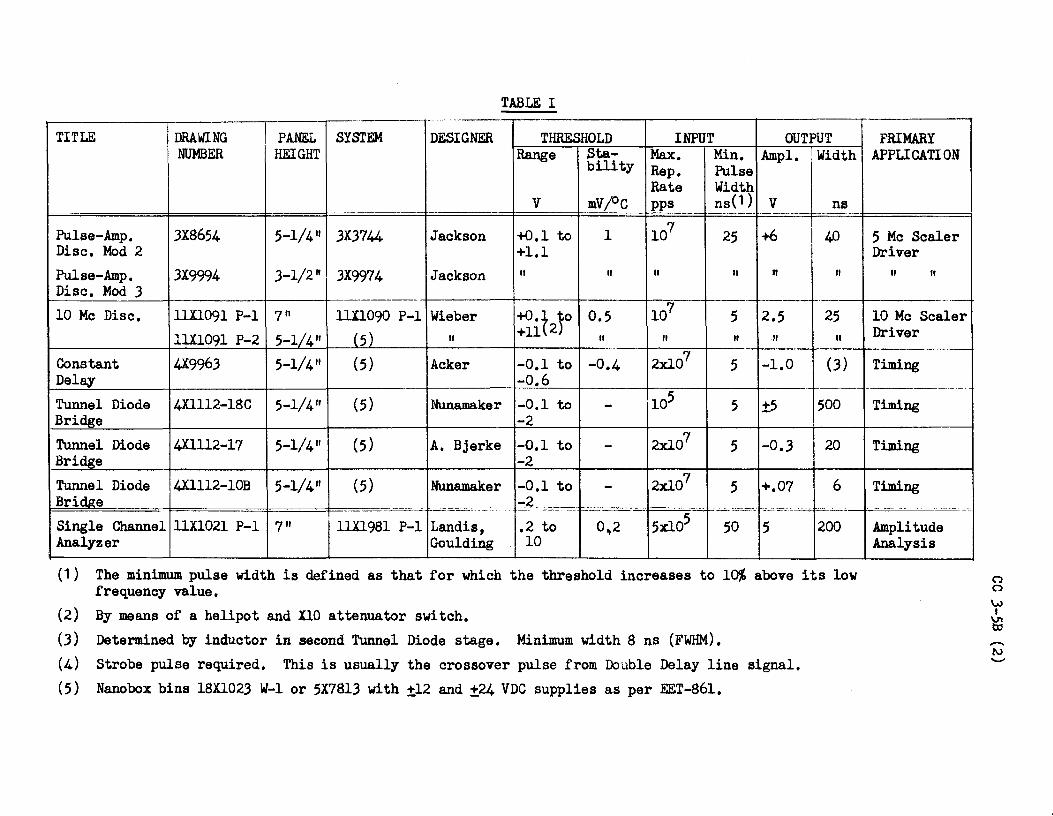
TABLE I --------r------.-----.,--------·-T-···· ·---------------~------,.--------.---------T
TITLE
Pulse-Amp. Disc. Mod 2 Pulse-Amp. Disc. Mod J
DRAWING NUMBER
JX8654
JX9994
PANEL SYSTEM HEIGHT
5-1/4 11 JXJ744
J-1/2 1' JX9974
DESIGNER
Jackson
Jackson
THRESHOLD INPUT OUTPUT Range Sta- Max. Min. Ampl. Width
bility Rep. Pulse
v +o.l to +1.1 II
Rate Width mV/OC pps ns(1) V
1
II II II "
ns --- -
II
PRIMARY APPLICATION
5 Mc Scaler Driver
II II
1--------+-------+----+-------+------t----+----+-----,~------ -----~----+------- -· ----
10 Mc Disc. 11Xl091 P-1 7" 11Xl090 P-1 Wieber +o.i to 0.5 107 5 2.5 +11{2)
II
25 II
10 Mc Scaler Driver 11Xl091 P-2 5-1/4 11 (5) II II "
1--------+---'----+--''---'-'--+---'-"'-'----+-----+----+-----+---=--+---~---+--~--1-----~--~
Constant 4X996J 5-1/4 11 (5) Acker -0.1 to -0.4 2xl07 5 -1.0 (J) Timing Delay -0.6 1---.:..__----+-------+----+------+------t--~---+-----t----,---+----r--------------·--
Tunnel Diode 4Xlll2-18C 5-1/4 11 (5) Nunamaker -0.1 to - 105 Bridge -2 Tunnel Diode 4Xlll2-17 5-1/4" Briruze Tunnel Diode 4Xlll2-10B 5-1/4 11
Bridae Single Channel 11Xl021 P-1 7" Analyzer
(5) A. Bjerke -0.1 to -2
5 ±5 500
2xJ.07 5 -0.J 20
2x10⁷ 5 +.07 6
(1) The minimum pulse width is defined as that for which the threshold increases to 10% above its low frequency value.
(2) By means of a helipot and XlO attenuator switch. (J) Determined by inductor in second Tunnel Diode stage. Minimum width 8 ns (FWHM). (4) Strobe pulse required. This is usually the crossover pulse from Double Delay line signal. (5) Nanobox bins 18Xl02J W-1 or 5X7813 with ±12 and ±24 VDC supplies as per EET-861.
Timing
Timing
Timing .----·- - ·--·
Amplitude Analysis
-I\) -

File No. CC 3-lOA (1) H. G. Jackson Rev. December 15, 1963 E. W. Pullen
Lawrence Radiation Laboratory, University of California, Berkeley
I. SUMMARY
COUNTING NOTE
DUAL 3 CHANNEL POSITIVE INPUT COINCIDENCE AND
ANTI-COINCIDENCE UNIT MODEL 3
This unit is a transistor version of the Model 2 coincidence and anti-coincidence unit, and reference should be made to Counting Note CC 3-9A regarding the detail of the operation of this type of coincidence circuit.
Fig. 1 - Coincidence Unit Front View
II. SPECIFICATIONS
*
**
A. Inputs. 1. Three channel coincidence, positive pulses*, 3.0 V > E in> 0.25 V. 2. One channel anti-coincidence, positive pulses, 3.0 V > E in > 1.0 V. 3. Impedance = 125 ohms.
B. Outputs. 1. 300 millivolts negative for 250 millivolt input pulses with 5 ns
clipping (double delay time, ~ ns long line). 2. 600 millivolts negative for clipping greater than 10 ns.
3. Pulse width determined by clipping lines.** 4. Output impedance from emitter follower about 20 ohms. Emitter load
resistor = 125 ohms. 5. Time delay input to output is about 4 ns.
c. Sigma pulse width about 5 ns. Coincidence time about 4 ns.
Earlier models of this unit employed inverting pulse transformers in the coin-cidence inputs for operation with negative pulses.
Clipping time = 2 X electrical length of line.
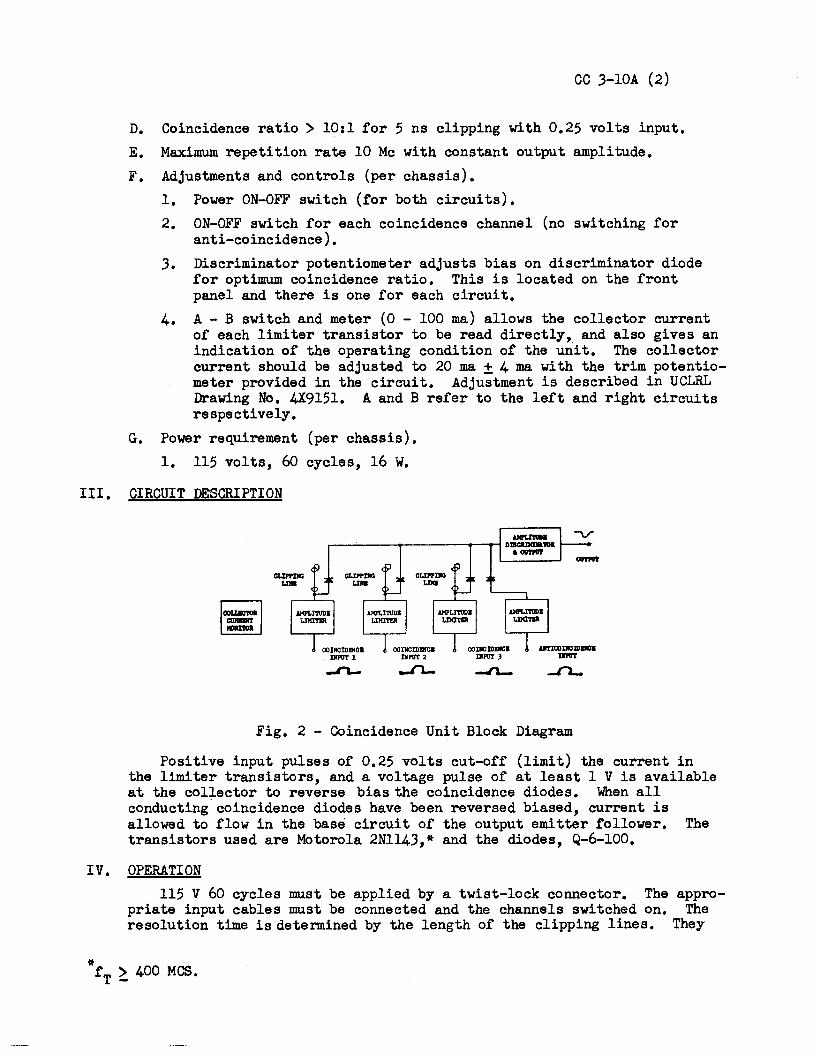
CC 3-lOA (2)
D. Coincidence ratio > 10:1 for 5 ns clipping with 0.25 volts input. E. Maximum repetition rate 10 Mc with constant output amplitude. F. Adjustments and controls (per chassis).
1. Power ON-OFF switch {for both circuits). 2. ON-OFF switch for each coincidence channel {no switching for
anti-coincidence). 3. Discriminator potentiometer adjusts bias on discriminator diode
for optimum coincidence ratio. This is located on the front panel and there is one for each circuit.
4. A - B switch and meter (0 - 100 ma) allows the collector current of each limiter transistor to be read directly,_ and also gives an indication of the operating condition of the unit. The collector current should be adjusted to 20 ma ± 4 ma with the trim potentio-meter provided in the circuit. Adjustment is described in UCLRL Drawing No. 4X9151. A and B refer to the left and right circuits respectively.
G. Power requirement {per chassis). 1. 115 volts, 60 cycles, 16 W.
III. CIRCUIT DESCRIPTION
.&1G'U11111 ~~~~.-~~~-.---.-IDlllCRJIGlll'IO& ·-
Fig. 2 - Coincidence Unit Block Diagram
Positive input pulses of 0.25 volts cut-off {limit) the current in the limiter transistors, and a voltage pulse of at least 1 V is available at the collector to reverse bias the coincidence diodes. When all conducting. coincidence diodes have been reversed biased, current is allowed to flow in the base circuit of the output emitter follower. The transistors used are Motorola 2Nll43,* and the diodes, Q-6-100.
IV. OPERATION 115 V 60 cycles must be applied by a twist-lock connector. The appro-
priate input cables must be connected and the channels switched on. The resolution time is determined by the length of the clipping lines. They
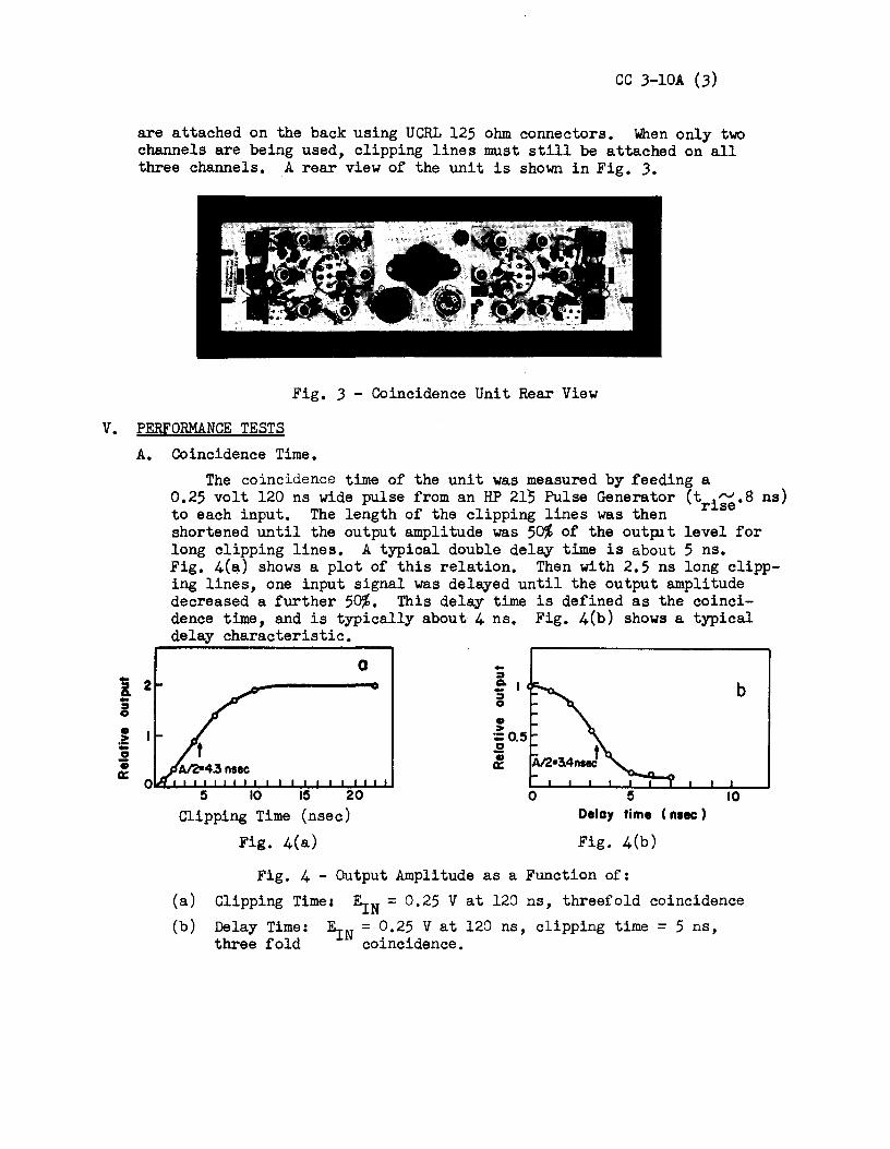
CC 3-lOA (3)
are attached on the back using UCRL 125 ohm connectors. When only two channels are being used, clipping lines must still be attached on all three channels. A rear view of the unit is shown in Fig. 3.
Fig. 3 - Coincidence Unit Rear View
V. PERfORMANCE TESTS A. Coincidence Time.
i 2 .. : : ;: 0 .. a:
The coincidence time of the unit was measured by feeding a 0.25 volt 120 ns wide pulse from an HP 21' Pulse Generator (t .""'.8 ns) rise to each input. The length of the clipping lines was then shortened until the output amplitude was 50% of the outpit level for long clipping lines. A typical double delay time is about 5 ns. Fig. 4(a) shows a plot of this relation. Then with 2.5 ns long clipp-ing lines, one input signal was delayed until the output amplitude decreased a further 50%. This delay time is defined as the coinci-dence time, and is typically about 4 ns. Fig. 4(b) shows a typical delay characteristic.
0
5 10 15 20 Clipping Time (nsec)
Fig. 4(a)
.. ::t Q. .. ::t 0
• > :;: 0.5 .S! t l. A/'l•3.4nsec
0 Delay time ( naec )
Fig. 4(b)
Fig. 4 - Output Amplitude as a Function of:
b
10
(a) Clipping Time: EIN = 0.25 V at 120 ns, threefold coincidence (b) Delay Time: EIN = 0.25 V at 120 ns, clipping time = 5 ns,
three fold coincidence.
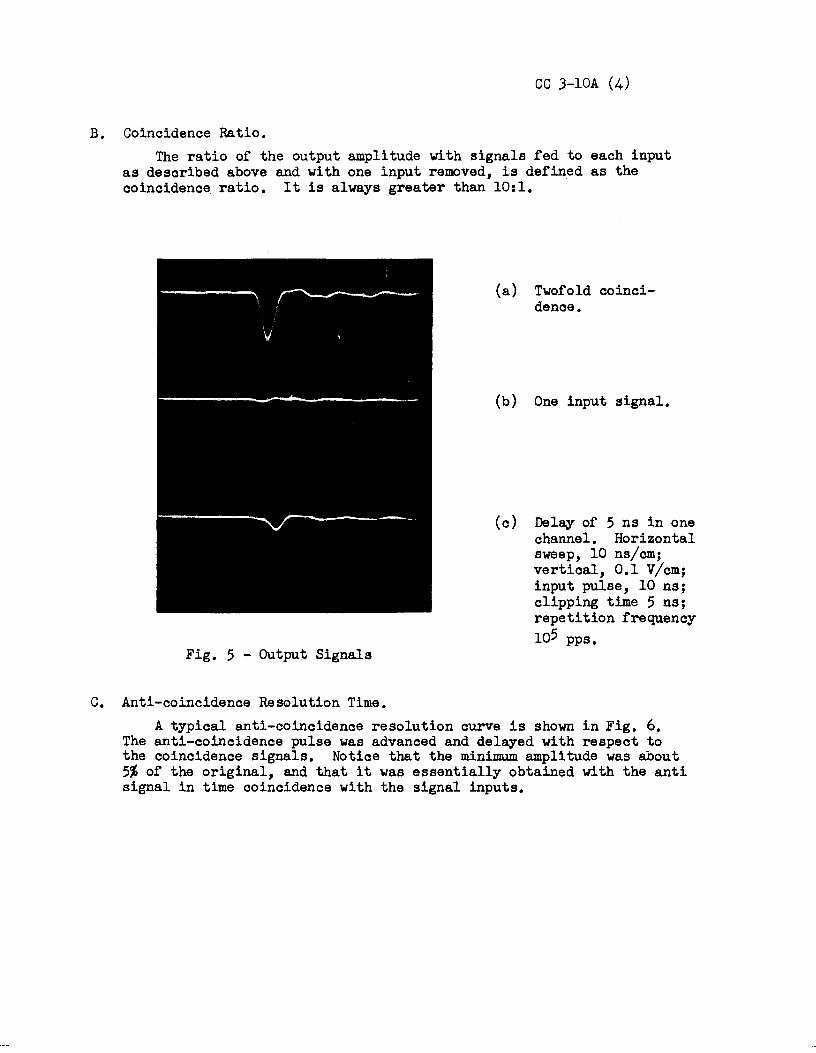
CC J-lOA (4)
B. Coincidence Ratio. The ratio of the output amplitude with signals fed to each input
as described above and with one input removed, is defined as the coincidence ratio. It is always greater than 10:1.
Fig. 5 - Output Signals
c. Anti-coincidence Resolution Time.
(a) Twofold coinci-dence.
(b) One input signal.
(c) Delay of 5 ns in one channel. Horizontal sweep, 10 ns/cm; vertical, 0.1 V/cm; input pulse, 10 ns; clipping time 5 ns; repetition frequency io5 pps.
A typical anti-coincidence resolution curve is shown in Fig. 6. The anti-coincidence pulse was advanced and delayed with respect to the coincidence signals. Notice that the minimum amplitude was about 5% of the original, and that it was essentially obtained with the anti signal in time coincidence with the signal inputs.

CC 3-lOA (5)
w 100~
0 90 ~ ~ 80 -_J 70 Q__
? 60
<( 50
f- 40 ~ Q_ 30 r-~ 20
0 10
-6 -4 -2 0 +2 +4 +6 +8 +10 +12 +14 +16 +18
DELAY-N SEC. Fig. 6 - Anti-coincidence Resolution.
Input pulse 1 V at 18 ns; clipping time 5 ns; repetition frequency 60 pps.
D. Effects of High Repetition Rates. A curve showing the change in the output pulse amplitude with
various input repetition rates is shown in Fig. 7. It will be noted that the maximum continuous repetition rate is, for practical pur-poses, about 25 Mc. For repetition rates below 10 Mc, the Nanosecond Pulse Generator was used with 20 ns clipping lines. Above 10 Mc, the Hewlett-Packard 608A oscillator was utilized, with the output amplified and limited by means of a H. P. 460A and 460B amplifier. The output of the 460B was then attenuated to the required amplitude.
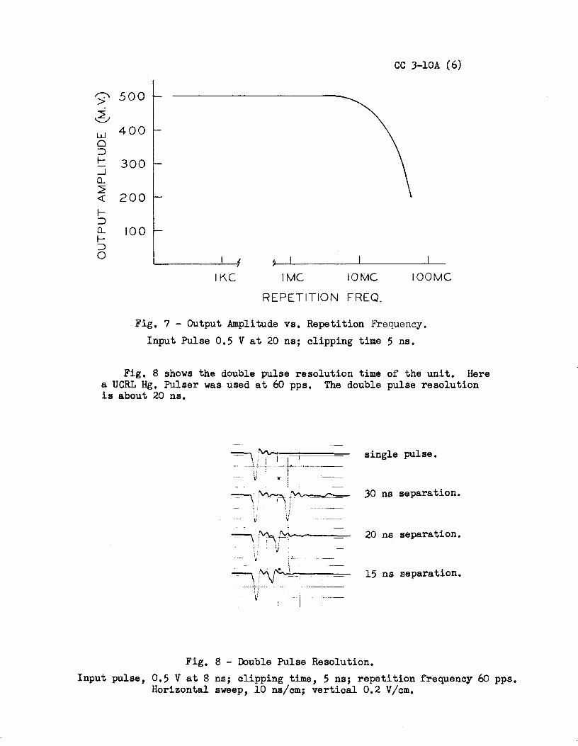
CC 3-lOA (6)
~ 500
6 w 400 0 ~ f- 300 _J CL ~ 4'. 200 r-~ CL 100 f-~ 0
IKC IMC IOMC IOOMC
REPETITION FREQ.
Fig. 7 - Output Amplitude vs. Repetition Frequency. Input Pulse 0.5 V at 20 ns; clipping time 5 ns.
Fig. 8 shows the double pulse resolution time of the unit. Here a UCRL Hg. Pulser was used at 60 pps. The double pulse resolution is about 20 ns.
M.. c -=--"'\ .• • IJI --+ I -'~-1 c ____ _
v ~ r--1 'V\.--!~ -=--'\ ' . '17 '' ----
J v i I
~ '~11~=-....-:, .. ·-=-=~ v v
-- •·I I --
-:-\.~ - v
single pulse.
30 ns separation.
20 ns separation.
15 ns separation.
Fig. 8 - Double Pulse Resolution. Input pulse, 0.5 Vat 8 ns; clipping time, 5 ns; repetition frequency 60 pps.
Horizontal sweep, 10 ns/cm; vertical 0.2 V/cm.

CC J-lOA (7)
E. Coincidence Resolution Curve. A test was made to determine the resolution time of the unit
operating in a two-fold coincidence system. Two 6810A photo-multiplier tubes were illuminated by a pulsed mercury light source. The pulse repetition frequency was 60 pps. Phototube signals were fed directly to the coincidence unit. The output signal was ampli-tude discriminated and the resultant output was counted on a scaler.
Fig. 9 shows a typical time resolution curve of one unit. Notice that on the sides of the curve the counting rate drops about a factor of 100 for l ns increase in delay.
_3000 c: ·e ... 1000 • Q. .. • ..!! 500 :I Q. -• 100 0 -0 ... -c: :I :so 8
-5 -3 -I 0 I 3 0
Delay ( nsec)
Fig. 9 - Resolution Time of Coincidence Circuit. Pulsed mercury light source; light level 1850 photons
at photocathode of tW'O 6810A photomultipliers.
REFERENCES 1. Counting Note CCJ-9, Fast J Channel Coincidence and Anti-Coinci-
dence Unit. 2. Transistor Counting Systems for Scintillation Detectors, Baker, etc.
UCRL 9000 February 17, 1960, also IRE Trans. on Nuclear Science, Vol. NS-7, June-September, 1960.
J. Schematic 4X85JJ. 4. Checkout and Adjustment Procedure - 4X9151. 5. Negative input model JX687J
EWP:mt

'ANj! Ct>INC" /AtPVT
-6..ZV
A B
-B.ZI/
ETCHED BOARo-i'i.1177Z BOARD OUTLINE 4}(gz.zz
4X~3Z
Fig. 10 - Schematic Circuit Diagram
-8.Zv'
~.LIV&./'' /Nevr
'.'~~11\/,C, 'Z ~ /1VPvr
"AIVT! C~1N.C ,. L'N.*vr

Iawrence Radiation laboratory, University of California, Berkeley
COUNTING NOTE
PULSE AMPLITUDE DISCRIMINATOR MODEL 2 AND 3
'S-Jt File No. C~ Page l November 211 1960 H. G. Jackson
ABSTRACT: This is an all semi-conductor modular unit capable of amvlitude discrimina-tion of pulses in the range O.l - 2.lv at repetition rates up to 10 p.p.s. The output signal is constant in amplitude, at approximately 8v1 and in rectangular shape, about 40 ns wide. The unit is primarily intended for driving the Decade Scaler Models 3141 or 5.1
The Model 2 and 3 Pulse Amplitude Discriminators are similar in function, the only difference being in physical size. The Model 2 is intended to fit a 5!11 card bin, along with the Model 3 or 4 Decade Scaler. The Model 3 plugs into the Jft' card bin, with the Model 5 Decade Scaler.
Fig. l Pulse Amplitude Discriminator Model 3
1 Decade Scaler Model 3 - l.Oµs resolution time, 5-i'' card bin. (Counting Note CC9-7A) II II II 4 - 0.2µs II II II tt 11 11 11 11
II 11 II 5 _ 0. 2p.s 11 11 J~ll II 11
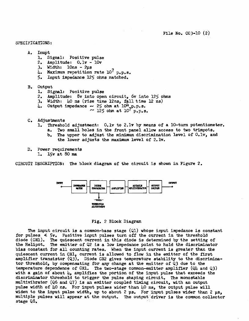
File No. CC3-10 (2}
SPECIFICATIONS:
A. Inupt 1. Signal: Positive pulse 2. Amplitude: O. lv - lOv 3. Width: lOns - 2µs 4. Maximum repetition rate 107 p.p.s. 5. Input impedance 125 ohms matched.
B. Output 1. Signal: Positive pulse 2. Amplitude: 8v into open circuit, 6v into 125 ohms 3. Width: 40 ns (rise time 12ns, ffi.ll time 12 ns) 4. Output impedance - 25 ohm at 104 p.p.s •
.- 125 ohm at 107 p.p.s.
c. Adjustments 1. Threshold adjustment: O.lv to 2.lv by means of a 10-turn potentiometer.
a. Two small holes in the front panel allow access to two trimpots. b. The upper to adjust the minimum discrimination level of O.lv, and
the lower adjusts the maximum level of 2.lv.
D. Power requirements 1. 15v at 80 ma
CIRCUIT DESCRIPTION: The block diagram of the circuit is shown in Figure 2.
DCl'ID&JIZ DKl>S .ASTABLI OllTFUT lllTCll OOMl'IJl&toR AHPLD'Illl llJLTIVIBR.t.TOR Dlll'nll
Fig. 2 Block Diagram
The input circuit is a common-base stage (Ql) whose input impedance is constant for pulses < 5v. Positive input pulses turn off the current in the threshold diode (CRl). The quiescent current in this diode is determined by the setting of the Helipot. The emitter of Q2 is a low impedance point to hold the discriminator bias constant for all counting rates. When the input current is greater than the quiescent current in CRl current is allowed to flow in the emitter of the first amplifier transistor (Q3). Diode CR2 gives temperature stability to the discrimina-tor threshold, by compensating for any change at the emitter of Q3 due to the temperature dependence of CRl. The two-stage common-emitter amplifier (Q4 and Q3) with a gain of about 4, amplifies the portion of the input pulse that exceeds the discriminator threshold to trigger the pulse shaping circuit. The monostable multivibrator (Q6 and Q7) is an emitter coupled timing circuit, with an output pulse width of 40 ns. For input pulses wider than 40 ns, the output pulse will widen to the input pulse width, up to about 2 µs. For input pulses wider than 2 µs, multiple pulses will appear at the output. The output.driver is the common collector stage QB.
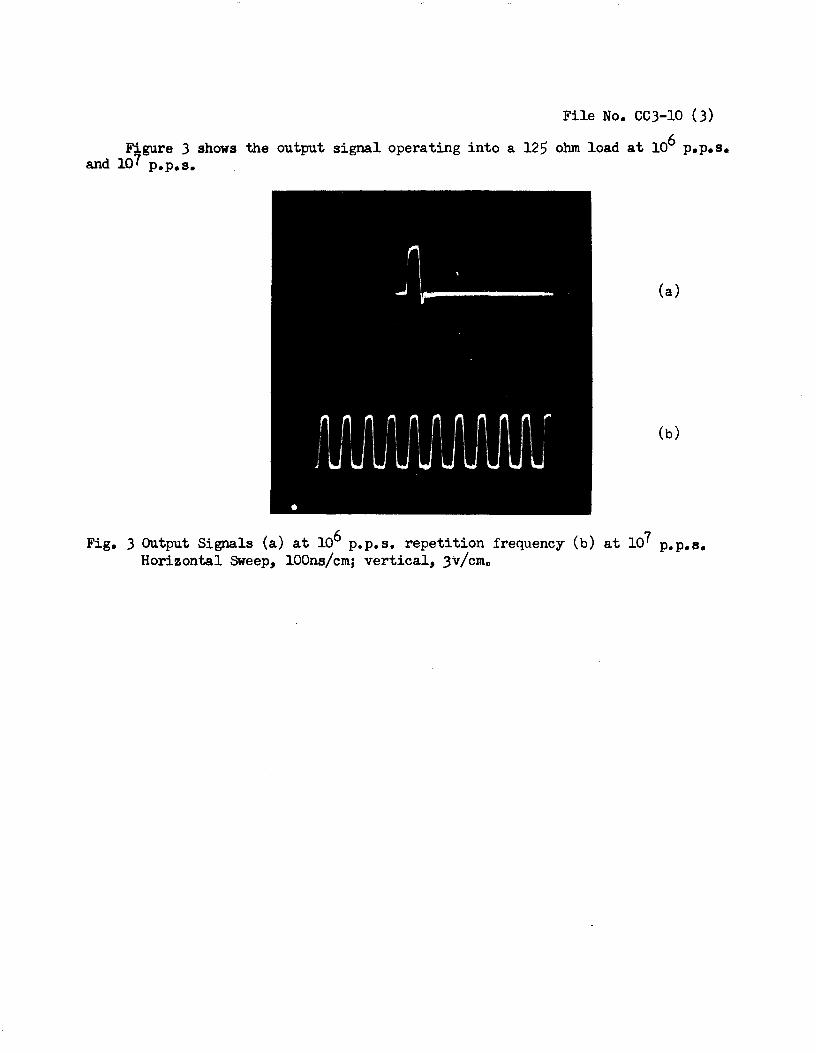
File No. CCJ-10 (3)
Figure 3 shows the output signal operating into a 125 ohm load at 106 p.p.s. and io7 p.p.s.
(a)
(b)
Fig. 3 Output Signals (a) at 106 p.p.s. repetition frequency (b) at 107 p.p.s. Horizontal Sweep, lOOns/cm; vertical, 3v/cmo
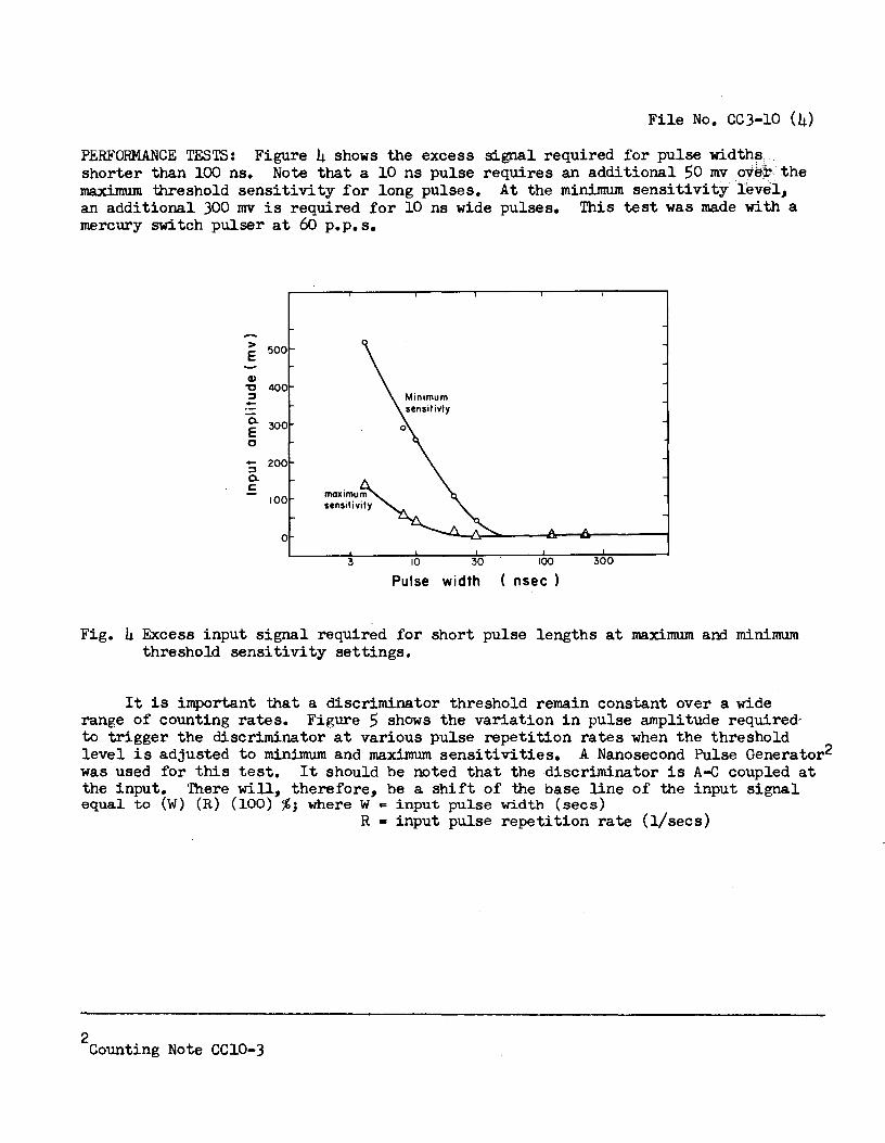
File No. CC3-10 (4)
PERFORMANCE TESTS: Figure 4 shows the excess signal required for pulse widths .. shorter than 100 ns. Note that a 10 ns pulse requires an additional 50 mv o:Ve:r the maximum threshold sensitivity for long pulses. At the minimum sensitivity level, an additional 300 mv is required for 10 ns wide pulses. This test was made with a mercury switch pulser at 60 p.p. s.
> 500 E Cl> "O 400 ::3
0. 300 E 0 - 200 ::3 0. c
100
0
3 10 30 100 300
Pulse width nsec )
Fig. 4 Excess input signal required for short pulse lengths at maximum and minimum threshold sensitivity settings.
It is important that a discriminator threshold remain constant over a wide range of counting rates. Figure 5 shows the variation in pulse amplitude required, to trigger the discriminator at various pulse repetition rates when the threshold level is adjusted to minimum and maximum sensitivities. A Nanosecond Pulse Generator2 was used for this test. It should be noted that the discriminator is A-C coupled at the input. There will, therefore, be a shift of the base line of the input signal equal to (W) (R) (100) %; where W • input pulse width (secs)
R • input pulse repetition rate (1/secs)
2 Counting Note CCl0-3
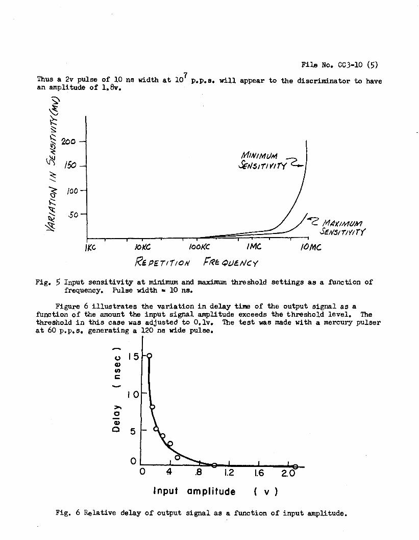
File No. CC3-10 (5) Thus a 2v pulse of 10 ns width at 107 p.p.s. will appear to the discriminator to have an amplitude of l.Bv.
~ ~ ~ ~ ~ ~ 200 ~
~ 15o ~ ..........
JOKC JooKC IMC
Re. Pf 711/0N ;:~~ t)t.JE.NCy
? /Y/IJtlMt/M Se1Vs1r1v1r'(
/OMC
Fig. 5 Input sensitivity at minimum and maximum threshold settings as a function of frequency. Pulse width • 10 ns.
Figure 6 illustrates the variation in delay time of the output signal as a function of the amount the input signal amplitude exceeds the threshold level. The threshold in this case was adjusted to O.lv. The test was made with a mercury pulser at 60 p.p.s. generating a 120 ns wide pulse.
-(J 15 Q) fl)
c: - 10 ~
0 Q)
0 5
Input om pl itude ( v )
Fig. 6 Relative delay of output signal as a function of input amplitude.
File No. CCJ-10 (6)
'IHRESHOLD STABILITY: The variation of threshold level with temperature is about l mv / 0c. This figure was checked by using a decade scaler card bin power supply. The temperature coefficient can be improved by as much as five times by using a power supply with improved temperature stability.
The threshold level should also drift not more than l mv/day at constant temperature.
0 The maximum operating temperature should be limited to 55 c.
REFERENCES:
1. Transistor Counting Systems for Scintillation Detectors, Baker, et al, UCRL 9000, February 17, 1960, also IRE Trans. on Nuclear Science, Vol. NS-7, June-September, 1960.
2. Schematic 3X8654 Pulse Amplitude Discriminator Model 2. Schematic 3X9994 Pulse Amplitude Discriminator Model J.

Q3 .?N 1143
04 2J\: !143
as 2N 1143
06 2N 1143
Q7 2N 1143
08 2N 706
't::: ~' ~11 20n jeT '::!:'.'. .1µro
7-45~FDr 06~~ Tl~~:v
Q6:J I .~,,, ki I !
__ .. t-------© I IL
O? 4.7K . 33Dil l ~:~r-%TM I 2N34 ·--l--1-TR-IMPO--T-1----l-------JL-__ .___ ____ ..._ __ _._ _____ __.,__ __ .__ __________ _._;_:_~p-H---~~~5V
MUB-402
Fig. 7 - Pulse Amplitude Discriminator
Q Q I w I
1--' 1--'
File No. CC 3-12 (1) January 10, 1964 H. G. Jackson
Lawrence Radiation Laboratory, University of California, Berkeley
COUNTING NOTE
4-WAY "AND II' 1 "INHIBIT II CIRCUIT - 11X2401 P-1
I. SUMMARY This unit is a direct-coupled 4-way diode "AND" circuit followed by
transistor amplification. One "INHIBIT" input is also provided, inhibiting any output. Standard +4 V logic levels are used. 1 Except for the parallel NPN-PNP output emitter-followers, all transistors are either off, or sat-urated on.
Provision is made for turning any of the 4 11AND 11 inputs off by means of toggle switches. 110 11 indicates the channel is off, inoperative.
The unit is packaged in a shielded nanobox. A size JX box (2-1/4 x 5-1/4" panel) is used.
Fig. 1 - 4-WAY AND, 1 INHIBIT, Circuit -- Front View II. SPECIFICATIONS
Input Impedance
"l" Level 110 11 Level
Power Reguired
1 K Q +4 v -1 v
Output Impedance
"l'' "0"
Delay
Rise-time +12 V 40 mA (90 mA max.) pin 10. -12 V 8 mA pin 21. Ground pin 1.
1 See CC 5-9 for logic voltage levels.
HGJ:mt
< 50 Q (50 rnA max.) +4 v -1 v
< 15 ns for pulse rise < 15 ns for pulse fall < 15 ns for step input
t/NLESS A/dT6.0 -/, A~L. R6.$1.$n:l~S
ARE" Y4 Wl4rr. 2. ""IL£. Ple:JOG~ C~6
"4R£ ~Pc:; 1147,
INPUTS
R// /OK
4-Way "AND 11 , 1 "INHIBIT 11 Circuit Schematic
R2.o /2.0...12 iw'
+ Cl =T 6.1},µf rh 35V
~~&j~ .__ ........ ---1 -I//
RI'/ 47.IZ q?.5 2Nll4~
R£2. /OK
ovr
0 0
\..v I ....,,
I\)

File No. CC 3-13 (1) January 13, 1964 H. G. Jackson
Lawrence Radiation Laboratory, University of California, Berkeley
COUNTING NOTE
5 WAY "OR 11 CIRCUIT - 11X2441 P-1
I. SUMMARY This unit is a basic 5 way diode "OR" circuit1followed by transistor
amplification; it uses standard 4 V logic levels. Except for the parallel NPN-PNP output emitter-followers, all transistors are either off or saturated on.
The unit is packaged in a shielded nanobox. A size 3X box (2-1/4 x 5-1/4 11 panel) is used.
Fig. 1 - 5 Way "OR" Circuit -- Front View
II. SPECIFICATIONS Input
Impedance 1 K Q +4 v -1 v
Output Impedance
"l" "0"
Delay Rise-time
< 50 Q ( 50 mA max. ) +4 v 111 11 Level
•'() 11 Level
Power H.eguired +12 V 40 mA (90 mA max.) -12 v 1 mA Ground
1 See CC 5-9 for logic voltage levels.
HGJ:mt
pin 10. pin 21. pin 1.
-1 v < 15 ns < 15 ns for step
input
(+4:r--,q;~/--~,Mf---l~K~~ I -;y CR/
~;I'<' P&-2 ,.4j-
-IV
~7
5./.k
4)1 ~z 2/'/&.!4 ......_____, 2N~34
DIOP.GS FPt; //<17 EXCcPT AS NIJTEP
5 Way "OR" Circuit Schematic
11? II /20.../l.. IW
t;4 f/l/114J
-/2V
File No. CC 3-14 (1) January 10, 1964 H. G. Jackson
Lawrence Radiation Laboratory, University of California, Berkeley
COUNTING NOTE
5-WAY FANOUT - ll.XZ781 P-1
I. SUMMARY This unit is intended to make more signal current available at the
standard +4 V logic level} The circuit is basically a current switch, with an emitter-follower driving five similar parallel NPN-PNP emitter-followers.
The unit is packaged in a shielded nanobox. A size JX box (2-1/4 x 5-1/4 11 panel) is used.
5 WAY FAN-OUT Cl: s
llX 2180PI
Fig. 1 - 5-WAY FANOUT -- Front View II. SPECIFICATIONS
Input Impedance
Output (5 similar outputs)
111 11 Level 110 11 Level
Power Required
1 KO +4 v -1 v
+12 V 50 mA (250 mA max.) pin 10. -12 V 20 mA pin 21. Ground pin 1.
1See CC 5-9 for logic voltage levels.
HGJ:mt
Impedance < 50 a (40 mA max. ) "l" +4 v 110 11 -1 v
Delay < 15 ns Rise Time < 15 ns (step input)
o _r+4-v
IN
/<IS 120..a. IW
t;J.5
Rl1 /OK
t/)I, Z,3, ~ ~ '1,,11,,1.1 : 2#8.14 - AIP/'/ 4)4, <.,8, 1q IZ, 14 : ZN 114~ - P/l/P ~R ~ z> a~+ = ,,:-p(I 114-,
V/llL£s_, N4T£P :-
1?4 I Ir(
"""" z. a(.l'T :4'
0 _r+9-J/
1. Rc51.S7"t::'Rs A.e& Y4W"9"T7: Clll<'4.tJA/ C<'MP.-.51o
~' S.t.k
rn
+4.3V
/?2.o 12.o.n. IW
t;J7
q:JLI
R2Z IOI<:
p~~
ot.rr 8' oI~""
+1211' 10
R'I R/£ Cl + IZ.o..rz. .,H~.../Z ~.$,.ul."1-th' ~w -f4.3j/ .J5/IPC
tf/3 (;';fl 5-/N14,4 rr;-0
4J4-
CZ ~ RI/ l"K 6.a,.,.,f'
3$VPC- - /Z y Z./
+/2V
RZ5 /<3o ~JS /20..IZ. 12.o...12. 1204. /W tW tW ~? ~II '115
,PIO 4)12. i$}/4
RZ7 R32 R37 /OK 10/f: '"K
-12V' .P<S-4 PcS!> ..... ~~
o_r-14 pvr c· or '~"'ovr o· oJ_,,.,.pvr c·
5-Way Fanout Schematic
File No. CC 3-15 (1) March 11, 1964 D. L. Wieber
Lawrence Radiation Laboratory, University of California, Berkeley
COUNTING NOTE
TIME-TO-HEIGHT CONVERSION SYSTEM - 11Xl5Bl P-1
I. SUMMARY This system converts the time interval, between the negative going edge
of a "start" pulse and the negative going edge of a "stop" pulse, into a linearly related pulse amplitude. See Fig. l. The output pulse is amplified and shaped so as to properly drive most pulse-height analyzers in use at LRL. With minor modifications this system can be used to measure time intervals ranging from 10 psec to 200 µsec.
Fig. 1 - Time-to-Height Converter System
II. SPECIFICATIONS All specifications are given with the unit as initially constructed for
a 100 nsec maximum time range. They are negligible functions of the maximum time range, except where noted. A. SYSTEM
1.
2.
J.
4.
Noise, FWHM
Stability
Linearity a. Integral
b. Differential Duty Cycle
4 psec jitter due to discriminator-shapers plus 20 mV amplifier noise, when driven by a mercury pulser through fixed delays. 2 psec/OC due to discriminator-shapers and con-verter, after 15 minutes warm up.
± 1% from 1 nsec to 100 nsec, see Section IIIA and Fig. 2. 1 ± 3%, as measured on a Delay Sweep unit (10Xl080P-l) lW, maximum.
10
~8 1--_J 06 2'
54 a.. I-:> 02
A 0
5
'(/)' 1--4 _J 0 ~
3 I-:> a.. 2 I-=> 0
0
0
0
B.A. GAJN : x I THRESH: O.O
20 40 60 80 100 TIME (ns)
8.A. GAIN : x 20
THRESH: O.O
A
0.4 0.8 1.2 TIME (ns)
0-2nS
1.6 2 .0
5
'W 4 I-_J 0 3 ~
I- 2 :::> a.. I-=> 0
0
5
~ I- 4 _J 0 2'
3
0
0
cc 3-15 (2)
B.A. GAIN : x 20 THRESH : 8.18
B
0.4 0.8 1.2 1.8 2.0 TIME (hS)
76-78hS
B.A. GAIN : x 20
THRESH : 10.0
0.4 0.8 1.2 1.6 2.0 TIME (n s) 95- 97ns
Fig. 2 - Discriminator Linearity. A, B, and C show 2 nsec windows expanded through the Biased Amplifier.
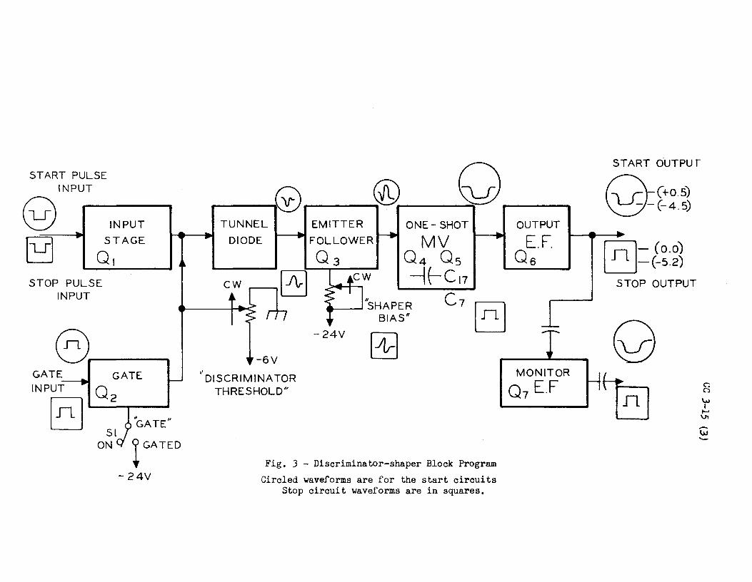
START PULSE INPUT
@ ~
INPUT STAGE
01 STOP PULSE
INPUT
GATE _.....,. INPUT
~ GATE
02
Sl ON ! GATED
-24V
•'
@ Q ----- ____ __,.. -----TUNNEL
DIODE
-6V
DISCRIMINATOR THRESHOLD"
EMITTER FOLLOWER
Q3
ONE- SHOT
MV Q4 Os -1t-C11
__ ____.'SHAPER C 7 BIASN
-24V
Fig. 3 - Discriminator-shaper Block Program Circled waveforms are for the start circuits
Stop circuit waveforms are in squares.
OUTPUT
E.F. Q6
MONITOR
01 E.F
ST ART OUT PU r
0-c+o.s) ~-(-4.5)
~- (o.o) L_J-(-5.2)
STOP OUTPUT
-w -
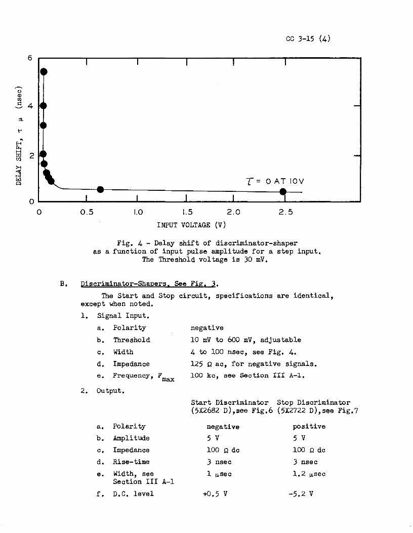
6
C) Q) tll s::: 4 ........
:i
~
... E-t Ii. H
2 :::z:: ti)
9 r:q 0
0 0
cc 3-15 (4)
T= OAT IOV
0.5 1.0 l.5 2.0 2.5
INPUT VOLTAGE (V)
Fig. 4 - Delay shift of discriminator-shaper as a function of input pulse amplitude for a step input.
The Threshold voltage is JO mV.
B. Discriminator-Shapers. See Fig. 3. The Start and Stop circuit, specifications are identical,
except when noted. 1. Signal Input.
a. Polarity b. Threshold c. Width d. Impedance e, Frequency, F max
2. Output.
a. Polarity b. Amplitude c. Impedance d. Rise-time e. Width, see
Section III A-1 f. D. C. level
negative 10 mV to 600 mV, adjustable 4 to 100 nsec, see Fig. 4. 125 Q ac, for negative signals. 100 kc, see Section III A-1.
Start Discriminator Stop Discriminator (5X2682 D),see Fig.6 (5X2722 D),see Fig.7
negative positive 5 v 5 v 100 Q de 100 Q de 3 nsec 3 nsec 1 µsec 1. 2 µsec
+o.5 v -5.2 v
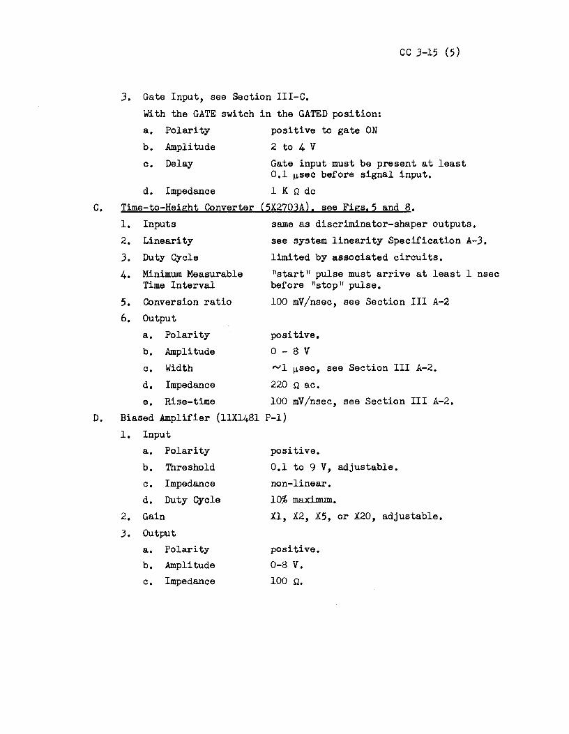
3. Gate Input, see Section III-C. With the GATE switch in the GATED position: a. Polarity b. Amplitude
positive to gate ON 2 to 4 V
cc 3-15 (5)
c. Delay Gate input must be present at least 0.1 µ.sec before signal input.
d. Impedance 1 K Q de c. Time-to-Height Converter (5X270JA), see Figs.5 and 8,
D.
1. Inputs 2. Linearity 3. Duty Cycle 4. Minimum Measurable
Time Interval 5. Conversion ratio 6. Output
a, Polarity b. Amplitude c. Width d, Impedance e. Rise-time
same as discriminator-shaper outputs. see system linearity Specification A-3. limited by associated circuits. "start" pulse must arrive at least 1 nsec before "stop" pulse, 100 mV/nsec, see Section III A-2
positive, 0 - 8 v Nl µ.sec, see Section III A-2. 220 Q ac. 100 mV/nsec, see Section III A-2.
Biased Amplifier (11Xl481 P-1) 1. Input
a. Polarity positive. b. Threshold 0.1 to 9 V, adjustable. c. Impedance non-linear. d. Duty Cycle 10% maximum.
2. Gain Xl, X2, X5, or x20, adjustable. 3. Output
a. Polarity positive. b. Amplitude 0-8 v. c. Impedance 100 Q.

FROM START SHAPER
@ FROM STOP SHAPER
+24V
-24V
CONSTANT CURRENT SOURCE
I I
~ . BOOTSTRAPPED
WHITE E.F. Q3,Q4
LINEAR GATE
Q6
®ROM STOP _...J
SHAPER
AMPLIFIERS . -. . GAIN :X3
H Q5,Q7,Q8,Q9
?X r LINK
y
Fig. 5 - Block Diagram of Time-to-Height Converter
.._ -- TO BIASED AMPLIFIER
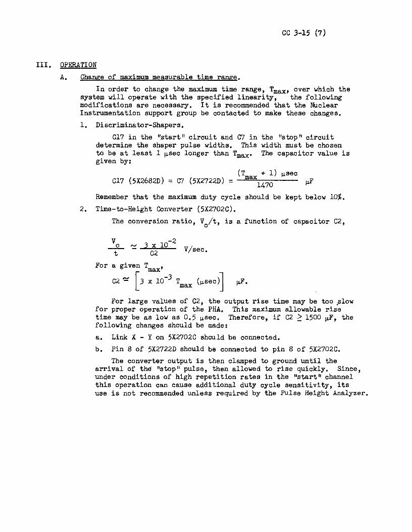
cc .3-15 (7)
III. OPERATION A. Change of maximum measurable time range.
In order to change the maximum time range, Tmax' over which the system will operate with the specified linearity, the following modifications are necessary. It is recommended that the Nuclear Instrumentation support group be contacted to make these changes. 1. Discriminator-Shapers.
Cl 7 in the "start" circuit and C7 in the "stop 11 circuit determine the shaper pulse widths. This width must be chosen to be at least 1 µsec longer than Tmax• The capacitor value is given by:
Cl? (5X2682D) = C7 (5X2722D) = (Tma:x: + 1) µsec 1470 µF
Remember that the maximum duty cycle should be kept below 10%. 2. Time-to-Height Converter (5X2702C).
The conversion ratio, V /t, is a function of capacitor C2, 0
v _o_ t
-2 ~ 3 x 10
C2 V/sec.
For a given T , max
C2 ~ [3 x 10⁻³ Tmax (µsec)] µF.
For large values of C2, the output rise time may be too fllow for proper operation of the PHA. This maximum allowable rise time may be as low as 0.5 µsec. Therefore, if C2 ~ 1500 µF, the following changes should be made: a. Link X - Y on 5X2702C should be connected. b. Pin 8 of 5X2722D should be connected to pin 8 of 5X2702C.
The converter output is then clamped to ground until the arrival of the "stop 11 pulse, then allowed to rise quickly. Since, under conditions of high repetition rates in the "start" channel this operation can cause additional duty cycle sensitivity, its use is not recommended unless required by the Pulse Height Analyzer.
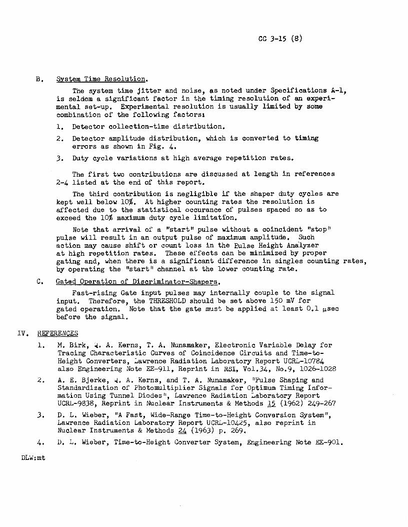
cc J-15 (8)
B. System Time Resolution. The system time jitter and noise, as noted under Specifications A-1,
is seldom a significant factor in the timing resolution of an experi-mental set-up. Experimental resolution is usually limited by some combination of the following factors: 1. Detector collection-time distribution. 2. Detector amplitude distribution, which is converted to timing
errors as shown in Fig. 4. J. Duty cycle variations at high average repetition rates.
The first two contributions are discussed at length in references 2-4 listed at the end of this report.
The third contribution is negligible if the shaper duty cycles are kept well below 10%. At higher counting rates the resolution is affected due to the statistical occurance of pulses spaced so as to exceed the 10% maximum duty cycle limitation.
Note that arrival of a "start 11 pulse without a coincident "stop" pulse will result in an output pulse of maximum amplitude. Such action may cause shift or count loss in the P.ulse Height Analyzer at high repetition rates. These effects can be minimized by proper gating and, when there is a significant difference in singles counting rates, by operating the "start" channel at the lower counting rate.
C. Gated Operation of Discriminator-Shapers. Fast-rising Gate input pulses may internally couple to the signal
input. Therefore, the THRESHOLD should be set above 150 mV for gated operation. Note that the gate must be applied at least 0.1 µsec before the signal.
IV. REFERENCES 1. M. Birk, ~. A. Kerns, T. A. Nunamaker, Electronic Variable Delay for
Tracing Characteristic Curves of Coincidence Circuits and Time-to-Height Converters, Lawrence Radiation Laboratory Report UCRL-10784 also Engineering Note EE-911, Reprint in RSI, Vol.34, No.9, 1026-1028
2. A. E. Bjerke, "Ii. A. Kerns, and T. A. Nunamaker, "Pulse Shaping and Standardization of Photomultiplier Signals for Optimum Timing Infor-m.a tion Using Tunnel Diodes'', Lawrence Radiation Laboratory Report UCRL-9838, Reprint in Nuclear Instruments & Methods 12. (1962) 249-267
J. D. L. Wieber, "A Fast, Wide-Range Time-to-Height Conversion System", Lawrence Radiation Laboratory Report UCRL-10425, also reprint in Nuclear Instruments & Methods ~ (1963) p. 269.
4. D. L. Wieber, Time-to-Height Converter System, Engineering Note EE-901.
DLW:mt
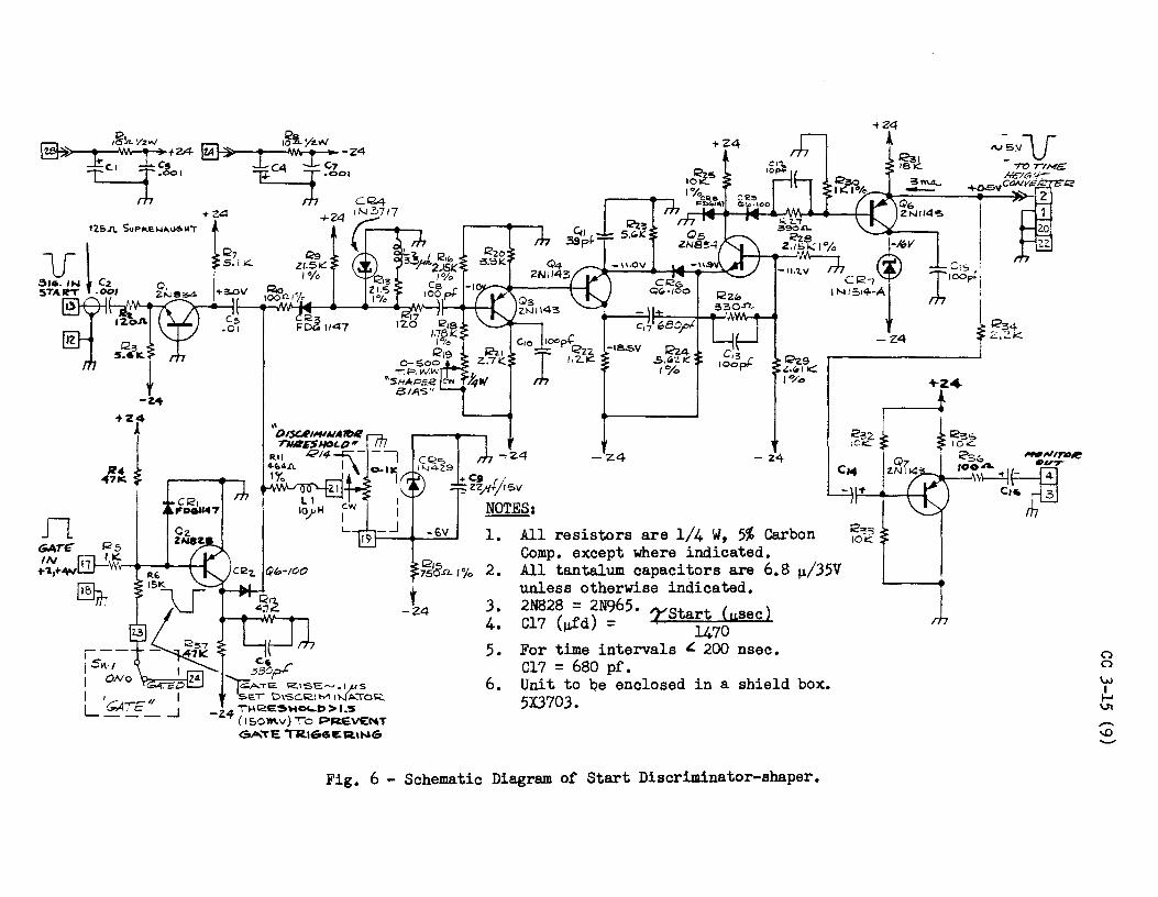
fl GATE '25 :~~.,~~·-r-e----4~-+-~
~
,--1s ... n I ONO
F~~ 1147
CQ<:;, f"J4Z9
-24
_,z4 t -Z4
Qz4 ,S,4Z."
l'Y'o 12-29 <::.i~ I IC l"Xco
- Z4 +C9 ' _ ZZfil/isv
NOTES: 1.
2.
3. 4. 5.
6.
All resistors are 1/4 W, 5% Carbon Comp. except where indicated. All tantalum capacitors are 6.8 µ/35V unless otherwise indicated. 2N828 = 2N965. Cl? (µfd) = ?"Sta~76usec) For time intervals £ 200 nsec. Cl?= 680 pf. Unit to be enclosed in a shield box. 5X3703.
Fig. 6 - Schematic Diagram of Start Discriminator-shaper.
-+24 !
rh

-Z.4
C.121 F061147
.+-Z.4
123 5.11::.
CZ 0.01
+ZA
QI Zt.5K. 1,-0
I !
3T
127 'Ll.S 1%
+Z4-
C5 CR4 -Z2t# tN4Z5 /SV
+24 +Z4
rZ4
122.5 5.i;.2.K lo/o
-2.4
- ... Cl/ ~.8f1./
~5V
-24 NOTES:
-Z4
1.
2.
3. 4.
5.
All resistors are 1/4 w, 5% Carbon Composition except where indicated. All tantalum capacitors are 6.8 µf /35V except where indicated. 2N828 = 2N965. C7 ( .. f'd) - Tstart (usec)/Stop (µsec) ....... - 1470 Start + .2 x lo-6 (µsec) For time intervals L. 200 nsec. C7 ~ 680 pf. Unit to be enclosed in a shield box 5X3703.
=
Fig. 7 - Schematic Diagram of Stop Discriminator-shaper.
0 0 w I ......
\.1l
......... ...... 0 '-'

11\lPUT FRo'""' STOP SHA.P~~· 5x~72.}
+?.4
124 615.!L 'o/o
R'5 z2r1.. ,_cJ,.;J -Z4V
+ 4v
c1<5 FD61147
CRE. FD.::.1147
NOTES:
+ '2.4v ~----....----)~ ...h~1a i..erif
I I
PL.A.C.E t:.18,1!:1, ?.o,z1, <'.:.LOSE 61o..10. "'IO PINS.
R'Z.7.. 'Z7 I(.
IU; \OIC'..
-l'Z.V
-Z4V
I
-2AV L ____ _ _J
5.
.. C"Zr i:;:;i T"'·S).\~ ei--....... ---->~
+74V
R. '2.'5 Cl'L + 1<!1 <\"70 "91SllK 1%
12'2." \,47~
'"· .. c13
'224 G.e)"& I.Bk::.
-Z.4V
CI" ~e,/A;- OUTPUT
__ ..;;+'-11-----~22
R31,n@J 4.71:'-
-12
1. 2. 3.
All resistors are 1/4 w, 5% unless noted. All tantalum capacitors are 6.8 µf/35V. 2N828 = 2N964 6.
7.
Connect X to Y and pin 8 of stop shaper to pin 8 of time height converter for C2>.0lµf. Unit to be enclosed in shield box 5X3703. Grounded pins are: 1,3,4,5,7,9,ll,13,15, 17,18,21,26. 4. Max mica. C2 = 300
Fig. 8 - Schematic Diagram of Time-to-Height Converter.
0 0 w I I-' 1..1\ -I-' I-' .........
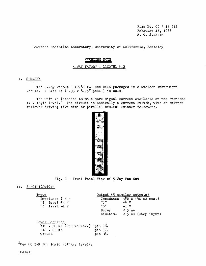
File No. CC 3-16 (1) February 15, 1966 H. G. Jackspn
Lawrence Hadiation Laboratory, University of California, Berkeley
COUNTING NOTE
5-WAY FANOUT - 11X2781 P-2
I. SUMMARY
The 5-Way Fanout 11X2781 P-1 has been packaged in a Nuclear Instrument Module. A Size lX (1.35 x 8.75" panel) is used.
The unit is intended to make more signal current available at the standard +4 V logic level. The circuit is basically a current switch, with an emitter follower driving five similar parallel NPN-PNP emitter followers.
Fig. 1 - Front Panel View of 5-Way Fan-Out
II. SPECIFICATIONS
Input Impedance 1 K n "l" level +4 V "o" level -1 V
Power Required +12 V 50 mA (250 mA max.) -12 V 20 mA Ground
1see CC 5-9 for logic voltage levels.
HGJ/mlr
Out ut (5 similar out uts Impedance <50 n O mA max.) "l" +4 v "O" -1 V Delay <15 ns Risetime <15 ns (step input)
pin 16. pin 17. pin 34.
0 J"~
IN
NOTES:
,t{/7 /(),/(
.I. ?/, 2, 3, _s; 7, ~It/~ = 2N8$1'- N..PN 2. 4>-9;~8,~/~.¥ =./IV//~3 ..PN..P .3. CR/.2,3,~ =.&~tS/N7
R~ /,I(
P~2 dur~H s+~v
0
.f.. _,,LL ~7#ER RE~Td;T5 A'RE 4 W CAR8t:w SJ' PN~&SS #&17',£4
R22 /{JI(.
R9 120..a.. /W
~
~
,It// /Ole
R27 /()/(.
Fig. 2 - Schematic 5-Way Fanout
/UZ 330.12.. /iw
~-l.3V
CHS IN7~9A
~12Y /6
-+ C1 -J~.84
3Sl/i)C.
r -/.2V
0 0
w I
~
File No. CC 4-6 (1) June 8, 1964 D. O. Hale
Lawrence Radiation Laboratory, University of California, Berkeley
COUNTING NOTE
SUMMARY OF PULSE HEIGHT ANALYZER MANUFACTURERS' DATA
The following table lists manufacturers' specifications for several Pulse Height Analyzers. Only those modes of operation that are considered somewhat standard have been listed, and special application features such as peak detection, area integration and time of flight have been ignored, The information was obtained from instruction manuals and advertising brochures.
Since all the units have not been evaluated, the table is for informational purposes only and does not constitute approval or disapproval.
DOH:mt

COUNT RANDOM ACCESS INPUTS PHA NUMBER CAPACITY EXTERNAL EXTERNAL MEMORY
MANUFACTURER OF PER DATA ADDRESS SUBGROUPS & MODEL CHANNELS CHANNEL ACCESS ACCESS TRANSFER
ND-101 256 105 Serial Serial 2 or 4 Parallel Manual or
Pulse ND-180FMR 512 106 Serial Serial 2 or 4
Manual or Pulse
PACKARD 400 105-106 Serial Serial 2 or 4 15 - 16 Manual or
Pulse RIDL 34-12 400 105-106 Serial Serial 2 or 4
Parallel Manual or Pnlco"'
RIDL 34-12B 400 105-106 Serial Serial 2 or 4 Parallel Manual or
p,,1 ~~
RCL 20631 400 105-106 Not Not 2 or 4 Listed Listed Manual or
Pulse TMC 401 400 106 Serial Serial 2 or 4
Manual or Pulse
VICTOREEN 200 105 Parallel Parallel 2 or 4 ST200 Manual or
Pulse VICTOREEN 400 106 Serial Serial 2 or 4 ST400uc Parallel Parallel Manual or
Pulse VICTOREEN 800 106 Serial Serial 8-4-2
ST800 Parallel Parallel Manual or Pulse
1Dead Time Varies (12 µ.sec plus 12 µ.sec per data decade shift). 2Signal jack labels indicated where possible.
ZERO MEMORY SUPPRESSION DATA ACCESS
CONTROL LOGIC TIME Yes Add Min 12 µ.sec
Sub Max 60 µ.sec 1
Yes Add 25 µ.sec Sub
Yes Add 12 µ.sec Sub Ext
Yes Add 12 µ.sec Sub
Yes Add 12 µ.sec Sub Rvt.
Yes Add 12 µ.sec Sub
Yes Add 39 µ.sec Sub
Yes Add 15 µ.sec Sub
Yes Add 15 µ.sec Sub
Yes Add 15 µ.sec Sub
DEAD TIME
.5 µ.sec per channel + Memory Access
Time .5 µ.sec per channel + Memory Access
Time .5 µ.sec per channel ± Memory Access
Time .5 µ.sec per channel + Memory Access
Time .5 µ.sec per channel + Memory Access
'T'i mo
.5 µ.sec per channel + 10 µ.sec + Memory Access Time .2 µ.sec per channel + Memory Access
Time .5 µ.sec per channel + Memory Access
Time .5 µ.sec per channel + Memory Access
Time .5 µ.sec per channel + Memory Access
Time
DEAD TIME
METER No
Yes
Yes
Yes
Yes
No
No
No
Yes
No
I l\) I
-l\)
STORE MODES READOUT MODES PHA MULTI- MULTI- SINGLE
MANUFACTURER CHANNEL CHANNEL CHANNEL SERIAL PARALLEL MODEL ANALYZER SCALER ANALYZER CRT PRINTERS PRINTERS RECORDERS
ND-101 Yes Yes No External Yes No Yes
ND-180FMR Yes Yes No External Yes Yes Yes
PACKARD Yes Yes No Internal Yes Yes Yes 15 - 16 RIDL 34-12 Yes Yes Yes Internal Yes Yes Yes
RIDL 34-12B Yes Yes Yes Internal Yes Yes Yes
RCL 20631 Yes Yes Yes External Yes Yes Yes TMC 401 Yes Yes No Internal Yes Yes Yes VICTOREEN Yes No No Internal Yes Yes Yes ST200 VICTOREEN Yes Yes Yes Internal Yes Yes Yes ST400uc
VICTOREEN Yes Yes No Internal Yes Yes Yes ST800uc
PUNCHED MAG TAPE TAPE No No
Yes No
Yes Yes
Yes Yes
Yes Yes
Yes No Yes -Yes No
Yes No
Yes Yes
INPUTS MULTI-SCALER MODE2
ADDRESS DATA ADVANCE INPUT GATE +4 V+O Amp or Co inc. -4 v Direct (Data 100 µsec only) -4 + 0 Ext is --+ 1 v -4 v + 0
+4 v -10 v -10 v --osc DET DET GATE -10 v -10 v -15 (off)
DC osc DET DET GATE -10 v -10 v -15 (off)
DC -10 v +10 v --+4 v -- ---- -- --
Scaler Strobe Advance -2 v ---5 v -8 v Same as Coinc. 25 µsec PHA (Data
Modes only)
I
0 0
.f:--1
°'
INPUTS PHA MODE2
PHA MANUFACTURER ANTI-
MODEL AMPLIFIER DIRECT GOING GOING
ND-101 -2 mV -J -JV (Off} Same as Full Scale +lOOV +JV (On} Coinc. @ Max Gain DC
ND-180FMR 0-100 mV -JV -4V (Off) Same as +lOV +4V (On) Co inc. +lOOV
PACKARD +20 mV +8V Prompt Prompt 15 - 16 Full Scale Delayed Delayed
@ Max Gain -8V +8V RIDL J4-12 +25 mV +6V Prompt Prompt
Full Scale +60V Delayed Delayed @ Max Gain -lOV +lOV
RIDL J4-12B +25 mV +6V Prompt Prompt Full Scale +60V Delayed Delayed (fll Max Gain -lOV +lOV
RCL 206Jl -10 mV +5V Single -Full Scale +15V Channel @ Max Gain +60V Mode
TMC 401 50 mV +15 v +4 v +4V Full Scale @ Max Gain
VICTOREEN Requires - - -ST200 Pre-amp
VICTOREEN -.5V +8V Pulse Pulse ST400uc Full Scale +80V Coinc. Coinc.
@ Max Gain -5V +5V VICTOREEN Requires - Prompt Prompt ST800 Pre-amp Delayed Delayed
-5V +5V
DC GATE ROUTING
Same as -4V + 0 Coinc. +4V
DC Same as +4V Coinc. DC
Blocking Not +8 (Off} Listed
Blocking +8V (Off)
+lOV
Blocking +lOV +8 (Off}
- Not Listed
- +4V
- Auto
- +lOV
- Auto
SINGLE CHANNEL MODE MULTI-
LOWER LEVEL UPPER LEVEL CHANNEL RANGE RANGE INPUT
- - -
- - -
- - -
15% of 80% of Same as Full Scale Full Scale PHA Mode
100% of 80% of Same as Full Scale Full Scale PHA Mode
100% of 100% of Same as Full Scale Full Scale PHA Mode
- - -
- - -
100% of 100% of Same as Full Scale Full Scale PHA Mode
- - -
PHYSICS POOL
EQUIPMENT
No
No
No
Yes
Yes
No
No
No
Yes
No
(") (")
t
Radiation Laboratory, University of California, Berkeley
COUNTING NOTE
DEFINITIONS OF PERFORMANCE MEASUREMENT
File No. CC5-6 Page 1 April 10, 1956 Frank Evans Quentin Kerns Dick Mack Revised Jan. 1, 1959
There is a need for conveniently evaluating the performance of equipment for which the rise time is an important factor. The definitions need to be characteristic of the equipment itself and not of the input signal. The following definitions are suggested as a way of quantitatively measuring the performance of circuits with available equipment. The ratios in signal levels are defined in terms that lend themselves to convenient measurement. The shortest usei'ul pulse for a piece of equipment is taken as a characteristic of the equipment. Two such pulses are de-fined below. However, none of the definitions are meant to exclude measurements which owing to suitable statistical techniques, may yield results that are a small fraction of times defined here.
A ~ Pulse is a pulse of constant amplitude which when applied to a circuit pro-duces an output whose peak amplitude is 50% of the output for a long input pulse.
LO:OO PULSE
SIGMA PULSE
INPUT
A
-0~ %
OUTPUT
f\ 2~ __ __,/ ~ _i_
The sigma pulse is specified by two numbers: (a) the length'!" in seconds and (b) the amplitude A, in volts. The time or occurrence "{'0 is taken as that instant on the rise when the amplitude reaches 50% peak amplitude.
For an amplifier the amplitude (A) is chosen as the value of the long input signal required to produce maximum unsaturated output (2B).
For a coincidence circuit the amplitude (A) is the minimum value of a long input signal required for normal maximum output (2B).
A Lambd.a ~ is defined for a triggered device and is a pulse whose amplitude (A) is twice the amplitude of the long pulse required to just trigger, and whose length is short enough so the device triggers on just half the input pulses, on the average.
INPUT OUTPUT
LO:OO ~J\ \_ PULSE
If\! 'l' /-\ ___ LAMBDA --~7~\ A
PULSE t rro
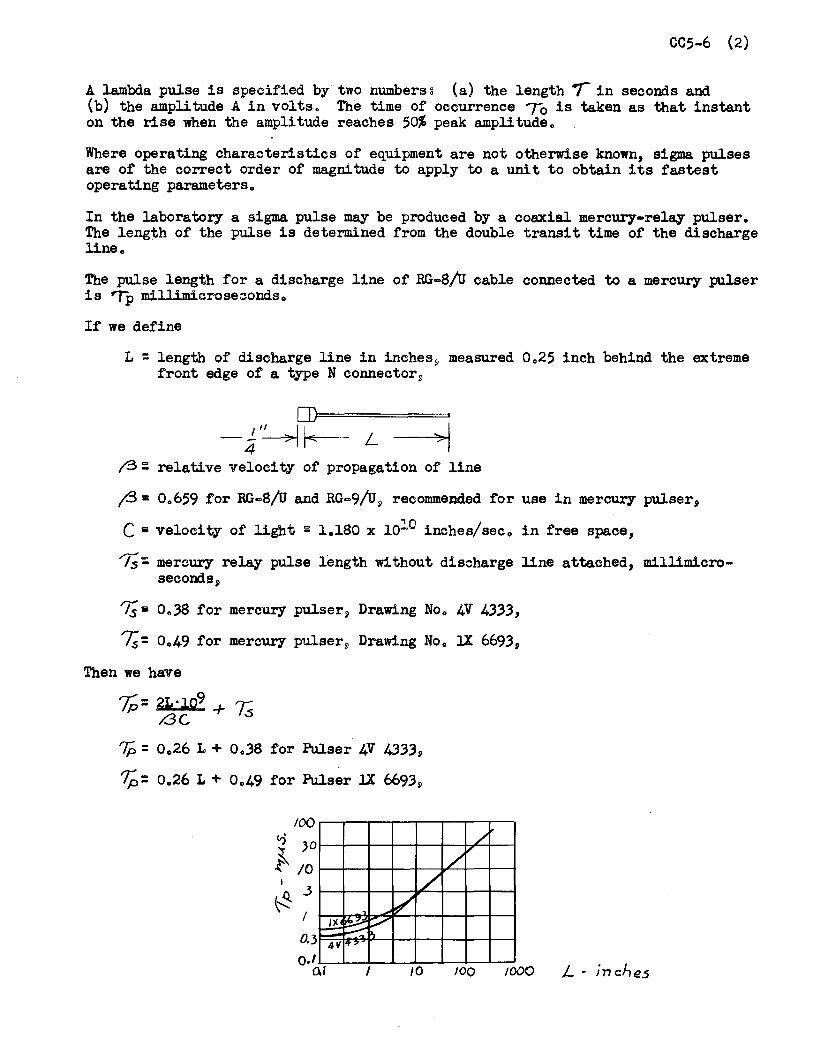
CC5-6 (2)
A lambda pulse is specified by two numbers 3 (a) the length "r in seconds and (b) the amplitude A in volts. The time of occurrence To is ta.ken as that instant on the rise when the amplitude reaches 50% peak amplitudeo
Where operating characteristics of equipment are not otherwise known, sigma pulses are of the coITect order of magnitude to apply to a unit to obtain its fastest operating parameterso
In the laboratory a sigma pulse may be produced by a coaxial mercury-relay pulser. The length of the pulse is determined from the double transit time of the discharge line.
The pulse length for a discharge line of RG-8/U cable connected to a mercury pulser is rrp millimicrosecondso
If we define
L = length of discharge line in inches 9 measured Oo25 inch behind the extreme front edge of a type N connector9
/3:: relative velocity of propagation of line
/3 = Oo659 for RG-8/U and RG-9/u~ recommended for use in mercury pulser,
C • velocity of light ~ 1.180 x io10 inches/seco in free space,
'7;:: mercury relay pulse length without discharge line attached, millimicro-seconds,
1°;; • 0.,.38 for mercury pulser~ Drawing Noo 4V 4.3.3.3,
rr;: 0.49 for mercury pulser~ Drawing Noo lX 669.3,
Then we have
%_,-::. 21·109 + ,,(3(, Ts
1P= Oo26 L + Oo.38 for Pulser 4V 4.3.3.3,
rp: 0.26 L + Oo49 for Pulser lX 669.3,
100
II) JO ~ 10
I
~ .3 I
0.3 0.1
-.fl'' ~
41/
O.I
/ - ~/ ~ v
I>. 1'1"7
I 10
/"' /'
JOO 1000 L - in ch~5
CC5-6 (3)
~ ~ is the interval between the sigma pulse applied to a circuit and the leading edge (at 50% amplitude) of the unsaturated output signal.
INPUT OUTPUT
DELA'( T//'v'f
Coincidence ~ is the ratio of the amplitude of output signal of a coincidence circuit when all inputs are fed sigma pulses in time coincidence, to the amplitude of the output signal when one of the input signals is absent.
For a coincidence -,anticoincidence circuit the coin~idence ratio is the ratio of the amplitude of the output signal when all coincidence input signals are in time coincidence, and anticoincidence signals are absent, to the amplitude when one coincidence signal is absent or one anticoincidence signal is present.
/, 2.
/.
2.
INPUT __/\ _ _/\_
~
OUTPUT _/\_L~A
COINCIDENCE lfA TIO::. A t B
~~r-
Coincidence ~ of a coincidence circuit is the minimum time delay required between one input sigma pulse and the remaining input sigma pulses to reduce the output amplitude response to 50% of the amplitude for zero delay, or, for a coincidence circuit, including an amplitude discriminator, the coincidence time is the minimum time delay required to reduce the counting rate of the output pulse to 50%. Resolu-tion time of a coincidence system is often defined as the time delay required between input pulses to produce a change in counting rate by one or two decades.
INPUTS OUTPUT
/. l
2. f
/.
2. ~ i ~INCIDENC.E TIME _/~--Q-lSr-~A
CC5-6 (4)
*Anticoincidence ~ of an anticoincidence circuit is the time delay required be-tween an input sigma pulse in the anticoincidence channel and input sigma pulses in the coincidence channels to reduce the output amplitude response to 50% of the amplitude for a very large delayo
INPUT OUTPUT
COINC, ~"' T >> 7Ac~ /NPUT(S) ANT/ C~O-l_N_C_.--+i-./'-\___ - -!/VPUT __,-· __ _
COINC, ~
//\/f::UT{5) ___/I \....
ANT' [QINC. I I INPUT I
~ 'fAc ANT/CO/fl/C1DENCE TIME
Recovery ~ is the minimum interval between the leading edges of two consecutive sigma pulses such that the trough between the output pulses is 50% or less of the peak amplitude Ai of the first pulse~ and the peak amplitude of the second pulse A2 is at least equal to the amplitude of the first pulse Ai.
INPUT OUTPUT
*Recoyerx ~ of an anticoincidence circuit is the minimum interval between input sigma pulses (one in the anticoincidence channel and the others all applied at the same time to the coincidence channels) which gives essentially the same output signal (A) as when the anticoincidence signal is absent.
* In general two figures will arise (one when the anti signal is early, and one when it is late); both of these figures should be specifiedo
CO!NCtQE/\/CE INPUT(5)
ANTI COl/\fC. INPUI
CO/NCID£NC£ //llPUT(5)
ANT!CO!NC, //VDUT
CC5-6 ( 5)
INPUT OUTPUT
l-o"-- TAR -----.ANTI C01NC. RECOVEI?'( TIME
Radiation Laboratory, University of California, Berkeley
COUNTING NOTE
DEFINITION OF PULSE TERMS
File No. CC5-7 Page 1 April 10, 1956 Quentin Kerns Dick Mack
The following definitions have been compiled from accepted sources covering pulse terminology commonly encountered at the laboratoryo
Background counts2 are counts caused by radiation corning from sources external to the counter tube other than the source being measured, or by radioactive contam-ination of the counter tube itself o
A clipping ~2 is a circuit for eliminating the tail of an electrical pulse after a predetermined time.
Counting ~ is the average number of pulses per unit of tirneo
A linear amplifier is a pulse amplifier in which the output pulse height is propor-tional to an input pulse height for a given pulse shape up to a point at which the amplifier overloadso Most linear amplifiers only approximately fulfill this de-finition.
A pulse is a momentary flow of energy.
A ~ am:glifier2 is an amplifier, designed specifically to amplify the intennittent signals incorporating appropriate pulse-shaping characteristics.
Pulse amplitudel is a term indicating the largest magnitude attained during the pulseo
Pulse dee~ time is the time required for an exponentially decaying pulse to fall t;"J7e of the peak amplitudeo
f!!.lse fall tirne2 is the time required for the instantaneous amplitude to fall from 90% to 10% of the peak amplitude.
A pulse·-·height discrirninator2 is a circuit designed to select and pass voltage pulses of a certain minimum amplitudeo
A pJJ.lse-heiJrot e~l.ecii.o.r2 is a circuit designed to select and pass voltage pulses in a certain range of arnplitudeso
~ .r.1Jag 11m~2 is the time required for the amplitude to rise from 10% to 90% or the peak amplitudeo
A randa.m .c.o..in..c.i~2 is one that is due to the fortuitous occurrence of unrelated counts in the separate detectors"
A register2 is an electromechanical device for recording or registering counts.
Saturation £urrent2 is the current which results when the applied potential is sufficient to collect all electrons.
Satu!Q.j!!,Q.~ YQ!!.§.G.~2 is the minimum value of applied potential required to produce saturation current.
~ . A scnler~ is a device thRt produces an output pulse whenever a prescribed number of input pulses hnve been received,, The number of input pulses per output pulse of

File No. CC5-7 (2)
a scaling circuit is termed the scaling factor. A binar:v scaler is a scaler whose scaling factor is two. A decade scaler is a scaler whose scaling factor is ten.
(_l) Standards on Pulses: Definition of Terms, Proc. I .R.E., Vol • .39, p. 624, June 1951.
(2)A Glossary of Terms in Nuclear Science and Technology, Published by A.S.M.E., 1955.
File No. CC 5-8B (1) F. Kirsten, Q. Kerns Rev. November 25, 1966 C. Kerns
Lawrence Radiation Laboratory, University of California, Berkeley
COUNTING NOTE
DEFINITIONS OF TERMS RELATED TO PHOTOTUBES
PART I
(1) IRE Standards on Electron Devices: Definitions of Terms Related to Phototubes, 1954, as published in the Proc. IRE, 42, 1277, August 1954.
(2) IRE Standards on Electron Tubes: Methods of Testing, 1962,as publishe~ in the 11 IRE Standards No. 62 IRE 7 .Sl. t1
PHOTOTUBE (1) An electron tube that contains a photocathode, and has an output depending
at every instant on the total photoelectric emission from the irradiated area of the photocathode. MULTIPLIER PHOTOTUBE (1) 1~
A phototube with one or more dynodes between its photocathode and the output electrode. PHOTOCATHODE (1)
An electrode used for obtaining photoelectric emission when irradiated. SEMI-TRANSPARENT PHOTOCATHODE (1)
A photocathode in which radiant flux incident on one side produces photo-electric emission from the opposite side. QUANTUM EFFICIENCY (Of a Phototube) (1)
The average number of electrons photoelectrically emitted from the photo-cathode per incident photon of a given wavelength. SENSITIVITY (Of a Photosensitive Electron Device) (2)
The quotient of the output quantity (such as current, voltagey etc.) by the incident radiant flux or flux density under stated conditions of irradiation. Note 1: This term is general and the measured value depends on many factors
such as spectral distribution of incident light, units used for measuring incident radiation, electrode under consideration, and output quantity, In several specific types of sensitivity the conditions of the test are more restricted. Where a well-defined specific sensitivity term is not applicable, caret must be taken to state all the pertinent conditions under which sensitivity is measured.
Note 2: If the output has some value in the dark, the dark value is subtracted from the output when irradiated.
* The terms Multiplier Phototube and Photomultiplier are equivalent and are used interchangeably.

CC 5-8B (2)
SENSITIVITY, Dn:IAMIC (Of a Phototube) (2) The quotient of the modulated component of the output current by the
modulated component of the incident radiation at a stated frequency of mod-ulation. Note: Unless otherwise stated the modulation waveshape is sinusodial. SENSITIVITY, RADIANT (Camera Tubes or Phototubes) (2)
The quotient of signal output current by incident radiant flux under specified conditions of irradiation. Note 1: Radiant sensitivity is usually measured with a collimated beam at
normal incidence. Note 2: The incident radiant flux is usually monochromatic at a given wave-
length. If the radiant flux is ·not monochromatic, its source must be described.
LUMINOUS SENSITIVITY (Of a Phototube) (1) The quotient of output current by incident luminous flux at constant
electrode voltages. Note 1: The term output current as here used does not include the dark current. Note 2: Since luminous sensitivity is not an absolute characteristic but
depends on the spectral distribution of the incident flux, the term is commonly used to designate the sensitivity to light from a tungsten-filament lamp operating at a color temperature of 2870oK.
CATHODE LUMINOUS SENSITIVITY (Of a Multiplier Phototube) (1) The quotient of photocathode current by incident luminous flux.
Note 1: The term photocathode current as here used does not include the dark current.
SPECTRAL CHARACTERISTIC (Of a Phototube) (1) A relation, usually shown by a graph, between the radiant sensitivity and
the wavelength of the incident radiant flux. ELECTRODE DARK CURRENT (Of a Phototube) (1)
The electrode current ·that flows when there is no radiant flux incident on the photocathode. Note 1: Since dark current may change considerably with temperature, temperature
should be specified. EQUIVALENT DARK-CURRENT INPUT (1)
The equal to Note 1:
incident luminous flux that would be required to give an output current the dark current. Since dark current may change considerably with temperature, temperature should be specified.
EQUIVALENT NOISE INPUT (Of a Phototube) (2) The value of incident luminous (or radiant) flux which, when modulated in a
stated manner, produces an rms signal output current equal to the rms dark-current noise both in the same specified bandwidth (usually 1 ·cps).
CC 5-8B (3)
CURRENT AMPLIFICATION (Of a Multiplier Phototube) (1) The
electric Note 1:
Note 2:
ratio of the output current to the photocathode current due to photo-emission at constant electrode voltages, Terms output current and photocathode current as here used do not include dark current. This characteristic is to be measured at levels of operation that will not cauae saturation.
GAS AMPLIFICATION FACTOR (Of a Gas Phototube) (1) The ratio of radiant or lruninous sensitivities with and without ionization
of the contained gas, TRANSIT TIME (Of a Multiplier Phototube) (2) (See also Part II LRL definitions.)
The time interval between the arrival of ljl. delta function light pulse at the entrance windo.w of the tube and the time at which the output pulse at the anode terminal reaches peak amplitude, TRANSIT TIME SPREAD (2) (See also Part II LRL definitions.)
The time interval between the half-amplitude points of the output pulse at the anode terminal, arising from a delta function of light incident on the entrance window of the tube.
PART II
LRL MULTIPLIER PHOTOTUBE DEFINITIONS
The definitions contained in Part II are divided into three groups. Group 1 of the definitions and standards is intended to provide a convenient way of estimating the usefulness of multiplier phototubes for precision timing applications. It defines quantities which when evaluated for a particular tube, give a measure of its spread or uncertainty in delay time. The spread or uncertainty in the delay time of a phototube pulse is a function of the size of the light signal as well as of parameters of the tube. Group 1 definitions refer to the overall tube.
In Group II, we consider separately:
a) the cathode to first dynode region (input electron optics)
b) the multiplier (set of dynodes)
c) the output structure (consists of signal-carrying leads from the anode and adjacent structures to the output pins or connector).
The function of the input electron optics (a) is to cause electrons emitted from the relatively large photocathode, to be directed into the multiplier. The multiplier (b) and output structure (c) are often considered together as a unit but should be considered separately in the case of multiplier tubes with coaxial output structures er slow-wave, i.e., (TW) output structures. The output structure forms the output signal pulse by extracting energy from the moving cloud of electrons leaving the last dynode.
To apply tbese definitions and standards to a particular tube, the operating voltage and voltage distribution must be specified.
Group I definitions are adequate for many users. Group II definitions added to Group I form a set intended for detailed discussion and evaluation of phototubes.
To aid in understanding these definitions related to phototubes, a brief outline is given to place them in one of six general categories of expressions directly concerned with time,

TIME CATEGORIES* ** PHOTOTUBE TERMS
CC 5-8B (5)
~DEVICE RISE TIME (DRT)
Rise Time ------- MULTIPLIER RISE TIME (MRT) OUTPUT STRUCTURE RISE TIME (ORT)
MULTIPLIER FALL TIME (MFT)
JDEVICE DELAY TIME (DDT) Delay Time -------1 MULTIPLIER DELAY TIME (MDT)
Fall Time --------
~DEVICE TRANSIT TIME (DTT)
Transi ~ Time------ CATHODE TRANSIT TIME ( CTT) MULTIPLIER TRANSIT TIME (MTT) OUTPUT STRUCTURE TRANSIT TIME (OTT)
DEVICE TIME SPREAD (DTS) Time Spread----------- PULSE TIME SPREAD (PTS)
CATHODE TIME SPREAD (CTS) MULTIPLIER TIME SPREAD (MTS)
JcATHODE TRANSIT TIME DIFFERENCE (CTTD) Transit-Time ------11 INTERDYNODE TRANSIT TIME DIFFERENCE (DTTD)
Rise Time as defined in CC 5-7 is the time required for the amplitude to rise from 10% to 90% of the peak amplitude. Fall Time as defined in CC 5~7 is the time required for the instantaneous amplitud~ to fall from 90% to 10% of the peak amplitude. Delay Time, in accordance with the usage of CC 5-6 is defined as the time interval between input and output as measured on the leading edge (at 50% amplitude) for an individual event. For the user, Transit Iime is a much more useful quantity than Delay Time, which is of interest primarily in photo-tube measurement technique. Transit Time is the average of the Delay Times measured for many events. It should be noted that transit times add linearly to get overall transit time and are independent of the number of electrons. Time Spread is the standard deviation of the distribution o~ Delay Times. Time Spreads add in an RMS fas hi on to get overall time spreads. ,Time Spreads vary in proporation to the inverse square root of the number of photoelectrons. They are given for single photoelectron ~vents.
Ari alternative method of expressing Time S;pread, is one which does not assume a Gaussian curve, but considers how the area under the time-spread curve is distributed. Using this method, one would define as the significant para-meter the minimum width of time slot which (properly centered), permits some percentage (e.g., 50%) of all output pulses to be counted. (For more information and actual values measured see UCRL-16540, Photomultiplier Single-Electron Time-Spread Measurements, by Cordon R. Kerns, October 3, 1966.)
**
Note differences between LRL definitions and the IRE Standards in Part I of this report. It is assumed that one is discussing a phototube which is not allowed to current saturate unless otherwise stated.
CC 5-8B (6)
Time Spread (Continued)
A certain freedom is taken in assuming that the distributions referred to in the phototube definitions may be approximated by Gaussian curves. However, the relative ease in combining Gaussian distributions compensates for this. The deviation of a distribution is often specified in terms of its full width at half maximum (FWHM) •. For a Gaussian distribution the FWHM is equal to 2.36 times the standard deviation. Transit-Time Difference expresses a systematic relationship between Transit-Time and position of illumination by photons or electrons. If we let (X,Y,Z) express the Cartesian coordinates of a point X, Y, Z on the photocathode or dynode, as the case may be:
Transit-Time Difference at point (X,Y,Z) =Transit Time at point (X,Y,Z) -Transit Time at point (X0,Y0,z0 )
where point Xo,Y0,zo is the reference position, and point (X,Y,Z) is the position where illumination strikes.
Transit-Time Difference may apply to electron trajectories in the photo-cathode-to-first dynode region or to electron trajectories in the region from one dynode to the next dynode. Although the Transit-Time Difference is found as the average of many events and is~therefore, independent of the number of electrons, the effect of Transit-Time Difference on the overall tube time spread varies as (number of electrons)-1/2. For simplicity, the transit-time differences may be included in the time-spreads, e.g. CTTD is included in CTS.
Group III of these definitions and standards covers aspects of tube operations other than terms involving timing.
GROUP I
DEVICE RISE TIME (DRT) The device rise time is the mean time difference between the 10% and 90%
points on the rise of the output voltage pulse for full cathode illumination by a short pulse of light. DRT includes the effects of Output Structure Rise-Time, Multiplier Rise-Time, time spreads, and time differences.
DEVICE DELAY TIME (DDT) The delay time from the instant at which a light pulse strikes the
envelope of the tube on its way to a given area of the cathode until the corresponding output pulse appears at the output connector of the tube is the device delay time for that area of the cathode. In accordance with tne other definitions, the output pulse is timed with respect to the 50% point of its leading edge. Unless otherwise stated, it is assumed that figures quoted for this quantity refer to the geometrical center of the useful cathode area.
GROUP I (Continued) DEVICE TRANSIT TIME (DTT)
CC 5-8B (7)
The average difference between the time at which an impulse of light strikes the envelope of a phototube on its way to the cathode and the time at which some specified point on the output pulse from the anode appears at the base pins or output connector of the tube. Neglecting the time of flight of light through the entrance window:
(DTT) = (CTT) + (MTT) + (OTT) Quotations of transit time should include specification of the point
on the output pulse to which the time measurements are made, such as the 50% peak amplitude point of the leading edge, centroid of the pulse, etc. Unless otherwise stated, all transit-time figures given in the Counting Handbook are referred to the 50% of peak amplitude point on the leading edge of the pulse.
DEVICE TIME SPREAD (DTS) When light signals result in the production of single photoelectrons from
randomly chosen areas of the photocathode, the corresponding anode delay times have a distribution about some mean value. The standard deviation of this distribution is the device time spread.
The device time spread may be measured by allowing light signals to produce single photoelectrons at known times, and to measure by means of an appropriate time coincidence circuit, the relative number of output pulses that occur in each unit interval following the light signal. Alternatively, the figures for cathode time spread (CTS) and multiplier time spread (MTS) may be combined (assuming that the distributions are Gaussian) to give the DTS of the tube as:
DTS + J CTS2 + MTS2
PULSE TIME SPREAD (PTS) When light signals producing other than one photoelectron are used, the
standard deviation of a Gaussian curve fitted to the distribution of delay times is approximately:
PTS = l/v1r° DTS = l//N MT '"'2 + 0
where N = the number of photoelectrons emitted per light pulse.
The purpose of the Group I terms is to describe the overall phototube in compact fashion. Where more detail is necessary, the Group II terms may be employed.

CC 5-8B (8)
GROUP II
CATHODE TRANSIT TIME (CTT) The mean delay time fro~ the cathode to the first dynode of photoelectrons
emitted from a given area of the photocathode is the cathode transit time for that particular area. Unless otherwise specified, it will be assumed that figures quoted for this quantity refer to the geometrical center of the useful cathode area.
CATHODE TRANSIT-TIME DIFFERENCE (CTTD) In general, the transit time for electrical output pulses resulting from
light pulses striking small areas of the photocathode is a function of the position on the cathode at which the light pulses strike. The cathode transit-time difference for a certain specified area of the cathode is the transit time for light pulses striking that area minus the transit time for light pulses striking a reference area of the cathode. When applicable, the reference ar~a is at the geometrical center of the useful photocathode area as specified by the manufacturer.
A note on technique:
I~ ma.king CTTD measurements, the diameter of the area illuminated is ·to be small compared to the distance over which an appreciable change in CTTD occurs. Normally CTTD is influenced primarily by the voltages applied .to the cathode, 'cathode focusing electrodes (if any), and the first few dynodes. These voltages should be specified since CTTD varies as the inverse square root of voltage.
Of course, a large value of CTTD is undesirable. The cathode shape and cathode to dynode optics are important parameters .for the manufacturers to optimize in order to minimize .CTTD over the range of operating voltage.
CATHODE TIME SPREAD (CTS) When single,photoelectrons are emitted from randomly chosen areas of the
photocathode, their respective delay times from the cathode to the first dynode have a distribution about some mean value, The standard deviation of a Gaussian curve fitted to this distributiqn is the cathode time spread.
The CTS results from two separate effects: cathode transit time differences, q.v., and spread in the initial emission velocities of photo-electrons~ The spread in initial velocity depends upon the wavelength of the incident illumination, the photoelectric work function, and the temperature,
If the cathode transit-time difference is large, the approximate value of cathode time spread may be derived from the cathode transit-time difference curves (by neglecting possible dynode 1 - dynode 2 transit-time differences.which are implicit in the cathode transit time differences, and effects due to velocities of emission).
CC 5-BB (9)
GROUP II (Continued)
MULTIPLIER RISE TIME (MRT) The multiplier rise time is the mean time difference between the 10% and
90% points on the rise of the current pulses entering the anode region and correlated with the entrance of single electrons into t.he multi plier, If the ORT << MRT, (as is commonly the case) the .MRT can be directly observed at the base pins or output connector of the tube,
MULTIPLIER FALL TIME (MFT) The multiplier fall time is the mean time difference between the 90% and
10% points on the fall C?_f the current pulses entering the anode region and correlated with the entrance of single electrons into the multiplier, If i,;he ORT << MFT, the MFT can be directly observed at the base pins or output connector of the tube,
MULTIPLIER DELAY TIME (MDT) The delay time from the instant an electron strikes dynode one until the
resulting pulse of charge appears at the anode of the multiplier is the multiplier delay time, In accordance with other definitions the delay is measured to the 50% point on the leading edge of the charge pulse,
MULTIPLIER TRANSIT-TIME (MTT) The mean value of the multiplier delay time is the multiplier transit
time, INTERDYNODE TRANSIT TIME_:DIFFERENCE (DTTD)
In general, the transit time for electrons leaving the nth dynode and striking the nth + 1 dynode depends on the position from which electrons leave the nth dynode. The interdynode transit time difference is the transit time for electrons leaving a given position minus the transit time for electrons leaving a reference position, Considering a cartesian coordinate system fixed in the dynode, we identify X, Y, Z as the point of emission and (X0,Y0,z0 ) as the reference point. Then: Transit-time difference at point (X,Y,Z) =Transit time at point (X;Y,Z) - Transit-time at point (X0,Y0,z0).
MULTIPLIER TIME SPREAD (MTS) When single photoelectrons, spaced in time, strike dynode one, the
corresponding output pulses have respective multiplier .delay times that are distributed about some mean value, The standard deviation of this distribution is the multiplier .time spread,
OUTPUT STRUCTURE RISE TIME (ORT) The output-structure rise time is the time difference between the 10% and
90% points on the rise of· the output voltage pulse arising from a narrow pulse of current striking the last dynode,
It depends on the transit time of electrons across the last-dynode to anode gap, and on the electrical pulse response of the anode-dynode output circuit, The dynode-anode transit time is calculated from geometry and voltage, while the electrical pulse response may be measured by applying pulses to the output ci:rcuit of the tube, or on a time-scaled analogue of the output circuitry, The output-structure rise time may be approximated by measuring the response of an illuminated phototube to a fast gating pulse applied to the latter dynode stages. (See CC 8-20,) The output-

CC 5-8B (10)
GROUP II (Continued)
structure rise time is essentially immune to statistical fluctuations from pulse to pulse, and for most present tubes is short compared to the time spreads CTS and MTS.
OUTPUT STRUCTURE TRANSIT TIME (OTT) The mean time interval between the entrance of a pulse of charge into the
anode region and the appearance of the corresponding electrical pulse at the . output connector or pins of the tube is the output structure transit time, In accordance with other definitions, the time interval is measured between the 50% points on the leading edge of the input and output pulses.
GROUP III
DC CURRENT GAIN OF A MULTIPLIER PHOTOTUBE Identical to definition of Current Amplification, Part I, of this Counting
Note,
PULSE CURRENT GAIN The mean ratio of the ~harge in the anode (or other, specified, output
electrode) current pulse to the charge in photoelectron current pulse leaving the cathode following a pulse of light that uniformly illuminates the useful area of the cathode as specified by the manufacturer,
The time duration of the pulse of light should not be greater than the transit time spr,ead of the phototube. Where the current gain is high enough, it is convenient t.o make the measurement with single photoelectrons.
In measuring the anode pulse charge, the effects of afterpulses should be disregarded ins0far as they can be distinguished from the main pulse.
It is important to note that the pulse current gain, on a pulse to pulse basis, unlike the current amplification, q.v., is a statistically varying quantity.
SATURATED OUTPUT CURRENT The maximum attainable value of anode (or other, specified, output electrode)
current as limited by space-charg~ saturation between one or more pairs of electrodes. According to Child's Law, this value of current varies as the three-halves power of voltage between the electrodes at which space-charge saturation occurs. Therefore, the saturated output current depends on the voltage distri-bution in the tubes which must be specified,
The measurement is usually made with a pulsed source of input current to the multiplier, such as a light pulser illuminating the cathode, The intensity of the current from the pulsed source is incr~ased until further increase in input current results in a negligible increase of output current, This level of output current is the saturated output current.
For the purposes of the counting notes, the point of "negligible" increase in output current is that level at which the rate of change of output current with input current is 1% or less of the maximum rate at any other input current.
CC 5-8B (ll)
GROUP III (Continued)
* MAXIMUM NON-SATURATED OUTPUT CURRENT The saturation of a multiplier phototube is not sudden ,or abrupt but
manifests itself as a gradual process. As saturation progresses, the output pulse amplitude tends to stop increasing, and insteaq the pulse width increases. For definit~ness, the peak pulse current at a 25% increase in pulse width (for a narrow light pulse) at th~ half-height is taken as the maximum non-satruated output current.
AFTERPULSES When an externally generated lighB pulse strikes the photocathode, a pulse
of photoelectrons leaves .. the phototcahode, is successively amplified at each succeeding dynode, and results in an output current pulse at the anode. Follow-ing this initial pulse, there may occur other pulses, called afterpulses, which are not caused by any externally generated light pulses, but rather by certain processes initiated by the original pulse.
NOISE PULSES (DARK) The portion of the Electrode Dark Current, q.v., which appears as
individual current pulses. Electrons r~leased from the cathode by thermionic emission and ion
feedbapk processes are major contributors to the noise pulse rate in multiplier tubes, Additional contributions to the noise pulse rate come from light generated within the tube, thermionic emission from ionization currents, and internal or external radioactivity.
COLLECTION EFFICIENCY. The ratio of the number of photoelections which actually contribute to
an anode (or other, specified, output electrode) current pulse to the total number of photoelectrons liBera_ted iS'·called the collection efficiency.
CK:mt
*
Not all photoelectrons released from the cathode necessarily reach the first dynode. The major contributing causes are chromatic aberration (initial velocity effects) in the 'photocathode - dynode one electron lens system, and other lens distortions particularly at the photocathode maximum diameter.
Some photoelectr9ns which do arrive at the first dynode do not necessarily result in an anode current pulse since secondary multiplication is a statistical process.
See LRL - Engineering Note.EE-795 for more information,
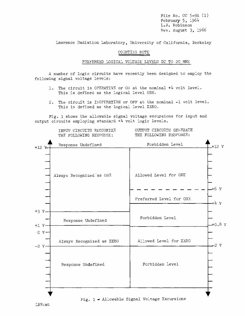
File No. CC 5-9A (1) February 5, 1964 L.B. Robinson Rev. August 3, 1966
Lawrence Radiation Laboratory, University of California, Berkeley
COUNTING NOTE
PREFERRED LOGICAL VOLTAGE LEVELS DC TO 20 MHZ
A number of logic circuits have recently been designed to employ the following signal voltage levels:
1. The circuit is OPERATIVE or ON at the nominal +4 volt level. This is defined as the logical level ONE.
2. The circuit is INOPERATIVE or OFF at the nominal -1 volt level. This is defined as the logical level ZERO.
Fig. l shows the allowable signal voltage excursions for input and output circuits employing standard +4 volt logic levels.
INPUT CIRCUITS RECOGNIZE THE FOLLOWING RESPONSE:
OUTPUT CIRCUITS GENERATE THE FOLLOWING RESPONSE:
+12 Y--t--~R_e_s_p_o_n_s_e~U_n_d_e_f_i_·n_e_d~~~~~~-r--~~~F_o_r_b_i_d_d_e_n~L_e_v_e_l~~~~~--l--'+l2 V
Always Recognized.as ONE Allowed Level for ONE
+6 v
Pref erred Level for ONE
Response Undefined Forbidden Level
0 v
Always Recognized as ZERO Allowed Level for ZERO
Response Undefined Forbidden Level
Fig. l • Allowable Signal Voltage Excursions LBR:mt
File No. CC 6-5B (1) Quentin Kerns f~ Harold Miller Revised: November 21, 1966 Harold Miller
Lawrence Radiation Laboratory, University of California, Berkeley
COUNTING NOTE
SPARK GAP TRIGGER AMPLIFIER
I. ABSTRACT
II.
The following trigger amplifier was designed to be used as a building block between low level logic circuits and spark chamber pulse modulators.
Described below is a 4-stage nonlinear amplifier which, when triggered by a 1 V signal, provides with minimum delay, an output pulse of sufficient energy to simultaneously trigger several spark gaps. The output pulse is produced by discharging a 1000 pF capacitance charged to 10 kV into a load. The pulse has a rise time of 10 ns and begins 32 ± 4 ns after the application of the 1 V input pulse. The trigger amplifier will operate at an average repetition rate of 0 to 50 pps and can be triggered in pulse bursts with a minimum of 5 msec between pulses.
SPECIFICATIONS
A.
B.
Ini::ut. 1. Impedance: .. "'5 Ort shunted by 2.8µH • 2. Connector: ENC. 3. Pulse Amplitude: 1 to 10 v. 4. Pulse Width: :::::. 1 nsec.
5. Rise Rate: ~ 1 V/nsec. -Out~uts.
1. Impedance: ·50r2. 2. Connectors:, Two Type HN. 3. Pulse Amplitude: -10 kV. 4. Pulse Rise Time: 10 nsec. 5. Pulse Decay Time: 25 nsec with both outputs terminated.
50 nsec with one output terminated. 6. Delay time between the input pulse and the beginning of the output
pulse: 32 ± 4 nsec @ 1 pps 35 ± 5 nsec @ 50 pps 38 ± 8 nsec @ 100 ppsl 50 pulse bursts. 45 ± 10 nsec @ 200 pps J

CC 6-SB (2)
c. Repetition Hate. 1. SO pps maximum average rate; any slower rate is acceptable. 2. Up to SO pulse bursts with a minimum of S msec. between pulses
with the average rate not exceeding SO pps. r~ the average pulse rate exceeds SO pps for an excessively long interval of time, the SGTA will automatically turn itself off. (See Section III, B 3). (See UCID-260S H. W. Miller 7-12-6S for complete description of overload-trip circuit).
D. DP-30 Monitor (PG-2). 1. Impedance: son. 2. Connector: BNC. 3. Pulse Amplitude: -lS V.
E. Output Monitor (PG-3). 1. Impedance: son. 2. Connector: BNC. 3. Amplitude: -10 V (Approximately 0.1% of the output pulse.)
F. Controls. a.c. on-off-overload reset switch located on the front panel. G. H.
Electrical Shielding. Power Requirements.
~ 120 db. 9S - 12S V rms 60 42 watts @ 0 pps. S4 watts @ SO pps.
cps.
III. DESCRIPTION
Figure 1 shows a front and rear vjew of the Spark-Gap Trigger Amplifier.
Fig. 1 - Spark-Gap Trigger Amplifier a) Rear View. b) Front Panel.
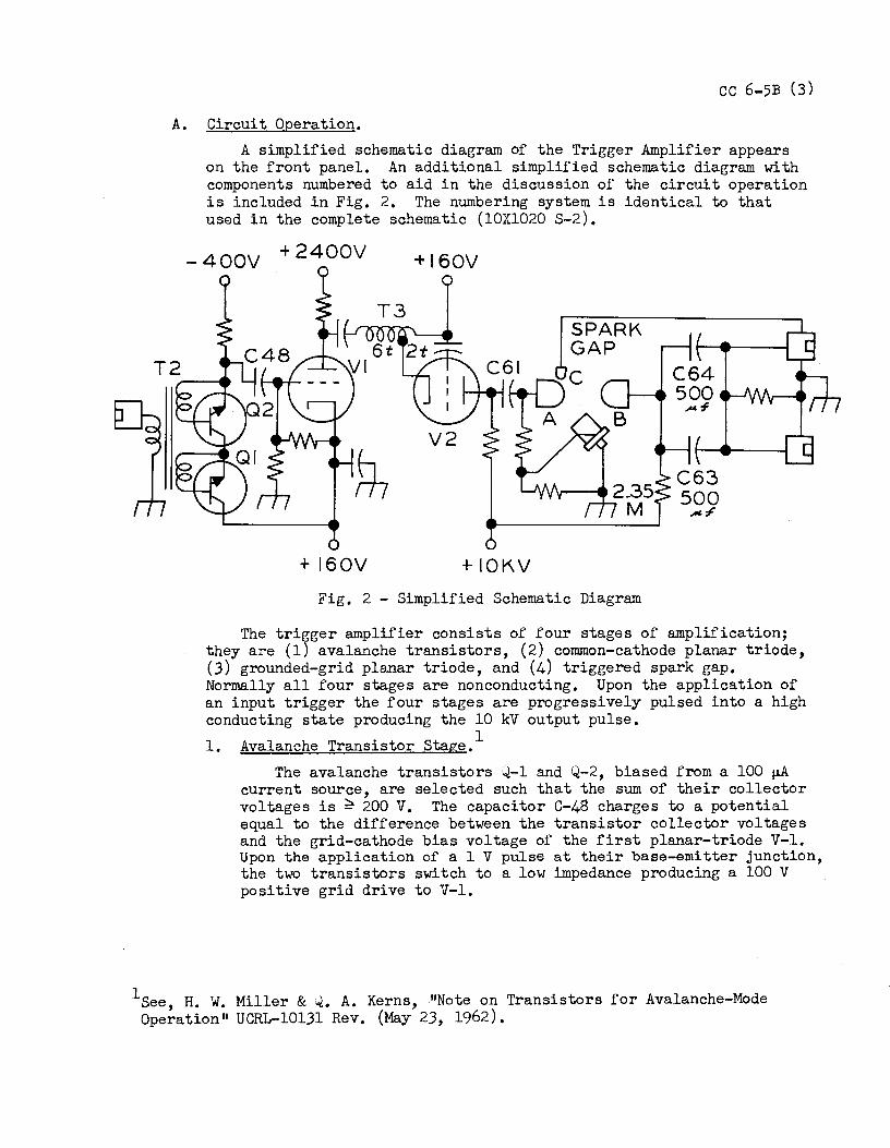
CC 6-5B (3)
A. Circuit Operation. A simplified schematic diagram of the Trigger Amplifier appears
on the front panel. An additional simplified schematic diagram with components numbered to aid in the discussion of the circuit operation is included in Fig. 2. The numbering system is identical to that used in the complete schematic (10Xl020 S-2).
+2400V
+ 160V +IOKV
SPARK GAP c
Fig. 2 - Simplified Schematic Diagram
The trigger amplifier consists of four stages of amplification; they are (1) avalanche transistors, (2) common-cathode planar triode, (3) grounded-grid planar triode, and (4) triggered spark gap. Normally all four stages are nonconducting. Upon the application of an input trigger the four stages are progressively pulsed into a high conducting state producing the 10 kV output pulse. 1. Avalanche Transistor Stage. 1
The avalanche transistors Q-1 and Q-2, biased from a 100 µA current source, are selected such that the sum of their collector voltages is ~ 200 V. The capacitor C-48 charges to a potential equal to the difference between the transistor collector voltages and the grid-cathode bias voltage of the first planar-triode V-1. Upon the application of a 1 V pulse at their base-emitter junction, the two transistors switch to a low impedance producing a 100 V positive grid drive to V-1.
1see, H. w. Miller & -t. A. Kerns, "Note on Transistors for Avalanche-Mode Operation" UCRL-10131 Rev. (May 23, 1962).
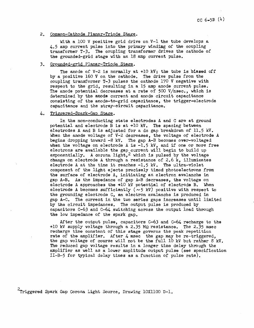
CC 6-5B (4)
2. Common-Cathode Planar-Triode Stage. With a 100 V positive grid drive on V-1 the tube develops a
4.5 amp current pulse into the primary winding of the coupling transformer T-3. The coupling transformer drives the cathode of the grounded-grid stage with an 18 amp current pulse.
3. Grounded-grid Planar-Triode Stage. The anode of V-2 is normally at +10 kV; the tube is biased off
by a positive 160 V on the cathode. The drive pulse from the coupling transformer T-3 pulses the cathode 170 V negative with respect to the grid, resulting in a 15 amp anode current pulse. The anode potential decreases at a rate of 500 V/nsec., which is determined by the anode current and anode circuit capacitance consisting of the anode-to-grid capacitance, the trigger-electrode capacitance and the stray-circuit capacitance.
4. Triggered-Spark-Gap Stage. In the non-conducting state electrodes A and C are at ground
potential and electrode B is at +10 kV. The spacing between electrodes A and B is adjusted for a de gap breakdown of 11.5 kV. When the anode voltage of V-2 decreases, the voltage of electrode A begins dropping toward -8 kV. The gap A-B becomes over-voltaged when the voltage on electrode A is -1.5 kV, and if one or more free electrons are available the gap current will begin to build up exponentially. A corona light,2 which is pulsed by the voltage change on electrode A through a resistance of 2.6 k, illuminates electrode A at the time it reaches -1.5 kV. The ultra-violet component of the light ejects precisely timed photoelectrons from the surface of electrode A, initiating an electron avalanche in gap A-B. As the impedance of gap A-B decreases, the voltage on electrode A approaches the +10 kV potential of electrode B. When electrode A becomes sufficiently (""5 kV) positive with respect to the grounding electrode c, an electron avalanche is produced in gap A-C. The current in the two series gaps increases until limited by the circuit impedances. The output pulse is produced by capacitors C-63 and C-64 switching across the output load through the low impedance of the spark gap.
After the output pulse, capacitors C-63 and C-64 recharge to the +10 kV supply voltage through a 2.35 Mn resistance. The 2.35 msec recharge time constant of this stage governs the peak repetition rate of the amplifier. After 4 msec the gap may be re-triggered, the gap voltage of course will not be the full 10 kV but rather 8 kV. The reduced gap voltage results in a longer time delay through the amplifier as well as a lower amplitude output pulse (see specification II-B-5 for typical delay times as a function of pulse rate).
2Triggered Spark Gap Corona Light Source, Drawing lOXllOO D-1.
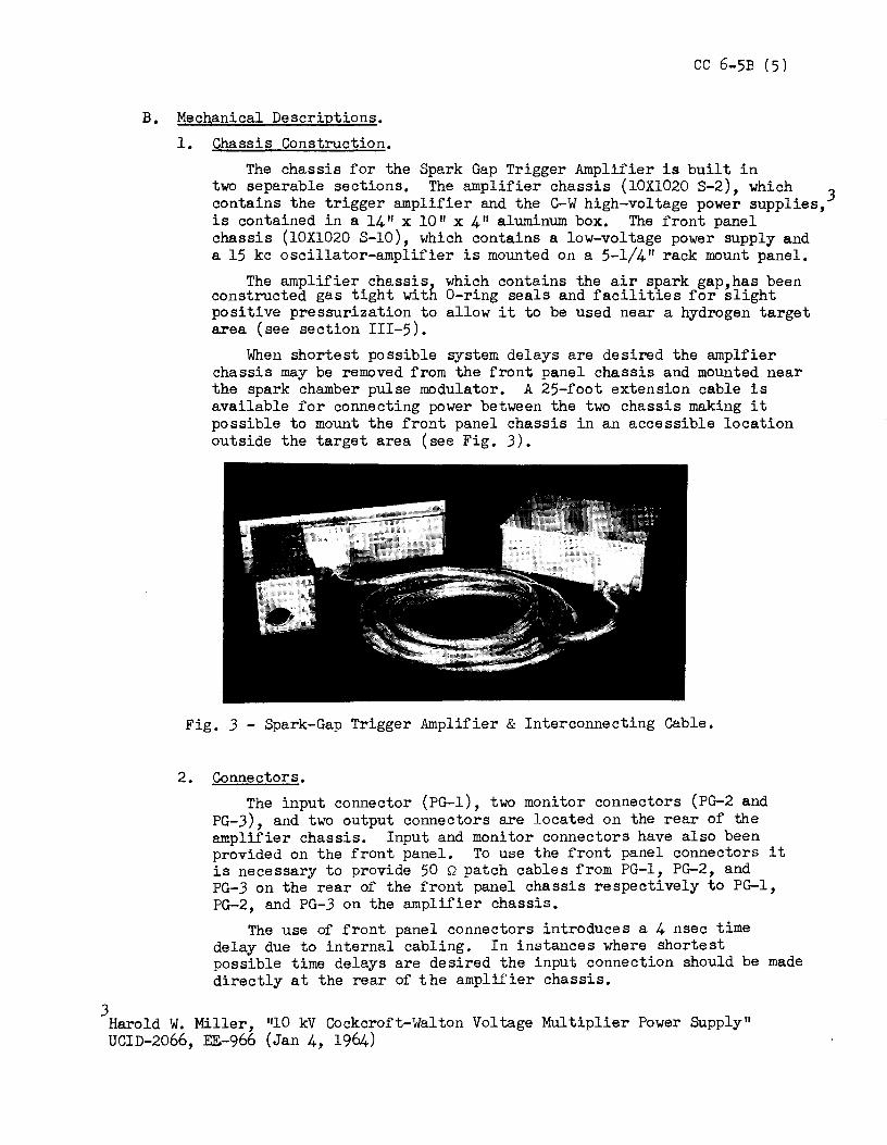
3
B. Mechanical Descriptions. 1. Chassis Construction.
CC 6-5B (5)
The chassis for the Spark Gap Trigger Amplifier is built in two separable sections. The amplifier chassis (10Xl020 S-2), which contains the trigger amplifier and the C-W high-voltage power supplies, 3 is contained in a 14 11 x 10 11 x 4 11 aluminum box. The front panel chassis (10Xl020 S-10), which contains a low-voltage power supply and a 15 kc oscillator-amplifier is mounted on a 5-1/4" rack mount panel.
The amplifier chassis which contains the air spark gap,has been constructed gas tight with 0-ring seals and facilities for slight positive pressurization to allow it to be used near a hydrogen target area (see section III-5).
When shortest possible system delays are desired the amplfier chassis may be removed from the front panel chassis and mounted near the spark chamber pulse modulator. A 25-foot extension cable is available for connecting power between the two chassis making it possible to mount the front panel chassis in an accessible location outside the target area (see Fig. 3).
Fig. 3 - Spark-Gap Trigger Amplifier & Interconnecting Cable.
2. Connectors. The input connector (PG-1), two monitor connectors (PG-2 and
PG-3), and two output connectors are located on the rear of the amplifier chassis. Input and monitor connectors have also been provided on the front panel. To use the front panel connectors it is necessary to provide 50 Q patch cables from PG-1, PG-2, and PG-3 on the rear of the front panel chassis respectively to PG-1, PG-2, and PG-3 on the amplifier chassis.
The use of front panel connectors introduces a 4 nsec time delay due to internal cabling. In instances where shortest possible time delays are desired the input connection should be made directly at the rear of the amplifier chassis.
Harold W. Miller, 1110 kV Cockcroft-Walton Voltage Multiplier Power Supply" UCID-2066, EE-966 (Jan 4, 1964)
CC 6-5B (6)
3. On-Off Switch
The on-off switch is located on the front panel. This switch is in series with the 117 V - 60 cps power line and the primary winding of the input power transformer. The power transformer is a Sola constant-voltage transformer. The input power can be from any 95 - 125 V, 60 cps power source. In instances where power is supplied from racks with line voltage regulators it is necessary that the regulated output be zeasonably near a sine wave.
The SGTA is nrotected from damage by an overload-trip circuit which turns off the high-voltage circuits if there is an overload condition (for example, an excessive input pulse rate.) The circuit can be reset by removing the cause of the overload condition and momentarily turning the front panel switch to reset and then back on. (See UCID-2605 H. w. Miller 7-12-65 for complete description of over-load circuit).
4. Indicator Lights.
The following two indicator lights are on the front panel:
(a) Green "on" light - when on, it indicat. es the presence of the 25.6 V from the low voltage power supply.
(b) Red "+10 kV" - this light when on indicates the +10 kV Cockcroft-Walton power supply is operating.
5. Gas Fittings.
Two 1/8" LRL gas fittings are located on the rear of the amplifier chassis. If the trigger amplifier is used in an area away from an explosive atmosphere the two fittings should be left vented to the atmosphere. In the event the amplifier is used near a hydrogen target area, air lines, one input and one exhaust, must be provided. Dry filtered air at a rate of 1 to 10 cc/min must be circulated through the spark gap compartment to remove contaminated air. This is especially true at high pulse rates.
IV. OPERATION.
A. Voltage Waveforms.
The voltage waveforms present at the input, the two monitors and the output are shown in Fig. 4. All impedance levels are 5on. The photographs are multiple exposures taken at 60 pps.
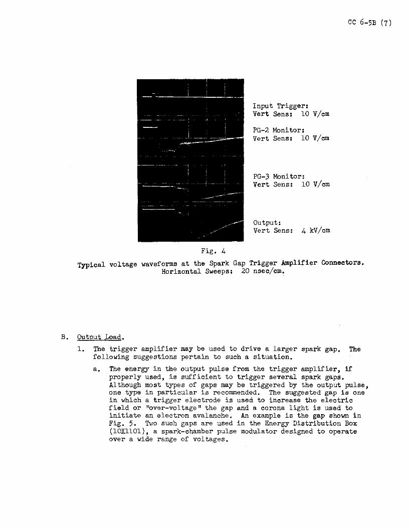
CC 6-5B (7)
Input Trigger: Vert Sens: 10 V/cm
PG-2 Monitor: Vert Sens: 10 V/cm
PG-.3 Monitor: Vert Sens: 10 V/cm
Output: Vert Sens: 4 kV/cm
Fig. 4 Typical voltage waveforms at the Spark Gap Trigger Amplifier Connectors.
Horizontal Sweeps: 20 nsec/cm.
B. Output Load. 1. The trigger amplifier may be used to drive a larger spark gap. The
following suggestions pertain to such a situation. a. The energy in the output pulse from the trigger amplifier, if
properly used, is sufficient to trigger several spark gaps. Although most types of gaps may be triggered by the output pulse, one type in particular is recomm.ended. The suggested gap is one in which a trigger electrode is used to increase the electric field or "over-voltage" the gap and a corona light is used to initiate an electron avalanche. An example is the gap shown in Fig. 5. Two such gaps are used in the Energy Distribution Box (lOXllOl), a spark-chamber pulse modulator designed to operate over a wide range of voltages.
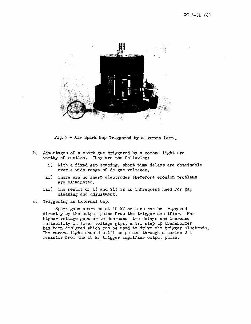
CC 6-5B (8)
Fig.5 - Air Spark Gap Triggered by a Corona Lamp.
b. Advantages of a spark gap triggered by a corona light are worthy of mention. They are the following:
i) With a fixed gap spacing, short time delays are obtainable over a wide range of de gap voltages.
ii) There are no sharp electrodes therefore erosion problems are eliminated.
iii) The result of i) and ii) is an infrequent need for gap cleaning and adjustment.
c. Triggering an External Gap. Spark gaps operated at 10 kV or less can be triggered
directly by the output pulse from the trigger amplifier. For higher voltage gaps or to decrease time del~s and increase reliability in lower voltage gaps, a 3:1 step up transformer has been designed which can be used to drive the trigger electrode. The corona light should still be pulsed through a series 2 k resistor from the 10 kV trigger amplifier output pulse.
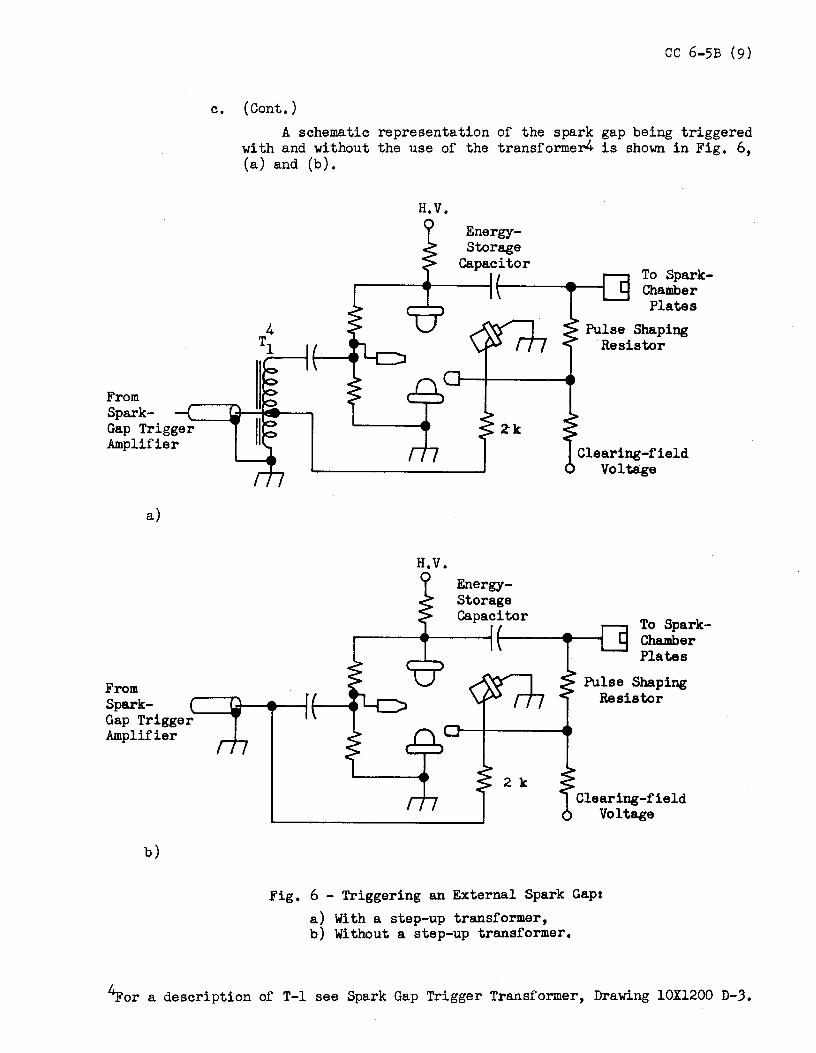
From Spark-Gap Trigger Amplifier
a)
From Spark-Gap Trigger Amplifier
b)
CC 6-5B (9)
c. (Cont.) A schematic representation of the spark gap being triggered
with and without the use of the transformer4 is shown in Fig. 6, (a) and (b).
H.V. Energy-Storage
Capacitor
H.V. Energy-Storage Capacitor
To Spark-Chamber Plates
Pulse Shaping Resistor
Clearing-field Voltage
To Spark-Chamber Plates
Pulse Shaping Resistor
Clearing-field Voltage
Fig. 6 - Triggering an External Spark Gap: a) With a step-up transformer, b) Without a step-up transformer.
~or a description of T-1 see Spark Gap Trigger Transformer, Drawing 10Xl200 D-3.
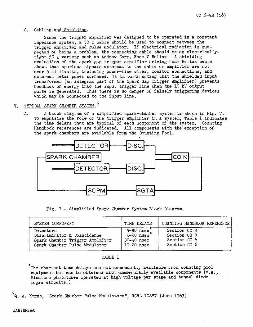
5
CC 6-5B (16)
C. Cabling and Shielding. Since the trigger amplifier was designed to be operated in a constant
impedance system, a 50 Q cable should be used to connect between the trigger amplifier and pulse modulator. If electrical radiation is sus-pected of being a problem, the connecting cable should be an electrically-tight 50 Q variety such as Andrew Corp. Foam V Heliax. A shielding evaluation of the spark-gap trigger amplifier driving foam Heliax cable shows that spurious signals external to the cable or amplifier are not over 5 millivolts, including power-line wires, monitor connections, and external metal panel surfaces. It is worth noting that the shielded input transformer (an integral part of the Spark Gap Trigger Amplifier) prevents feedback of energy into the input trigger line when the 10 kV output pulse is generated. Thus there is no danger of falsely triggering devices which may be connected to the input line.
V. TYPICAL SPARK CHAMBER SYSTEM. 5
A. A block diagram of a simplified spark-chamber system is shown in Fig. 7.
*
To emphasize the role of the trigger amplifier in a system, Table 1 indicates the time delays that are typical of each component of the system. Counting Handbook references are indicated. All co~ponents with the exception of the spark chambers are available from the Counting Pool.
c:::===IDETECTOR----DISC.
SPARK CHAMBER COIN.___-
i=======t DETECTOR.....______. DISC .
.__ ___________ SCPM1--------SGTA1----------~
Fig. 7 - Simplified Spark Chamber System Block Diagram.
SYSTEM COMPONENT TIME DELAYS COUNTING HANDBOOK REFERENCE Detectors 5-80 * Section cc 8 nsec* Discriminator & Coincidence 2-20 nsec Section cc 3 Spark Chamber Trigger Amplifier J0-40 nsec Section cc 6 Spark Chamber Pulse Modulator 10-20 nsec Section cc 6
TABLE 1
The shortest time delays are not necessarily available from counting pool equipment but can be obtained with commercially available components (e.g., Minature phototubes operated at high voltage per stage and tunnel diode logic circuits.)
Q. A. Kerns, "Spark-Chamber Pulse Modulators", UCRL-1ogg7 (June 1963)
QAK:HM;mt
File No. CC 6-6 (1) June 10, 1964 Q. A. Kerns H. W. Miller
Lawrence Radiation Laboratory, University of California, Berkeley
COUNTING NOTE
SPARK CHAMBER ENERGY DISTRIBUTION BOX
I. ABSTRACT The Spark Chamber Energy Distribution Box is a pulse generator designed
to provide high voltage pulses for energizing spark chambers. The important parameters of the circuit can be easily adjusted and/or changed for the best operation of spark chambers having a wide range of plate sizes, gap spacings, and filling gas mixtures,
Ten simultaneous output pulses are produced at ten type HN output connec-tors approximately 15 nsec after the applicati~n of a suitable input trigger (e.g., the output pulse from the Spark Gap Trigger Amplifier, CC 6-5).
An energy storage capacitor is in series, and a pulse shaping resistor is in parallel with each output connector, The storage capacitors are switched across their respective output loads by triggered spark gaps to produce the output pulses,
The amplitude of the output pulses can be varied from 0 to 20 kV by adjusting the spark gap spacings and the voltage of an external de power supply. The rise time of the output pulses, which is a function of the voltage and current switched, is typically 15 nsec. The pulse voltage is made to decay exponentially to prevent spurious sparks from forming in the spark chambers. Typical decay time constants, which range from 100 nsec to 800 nsec, can be varied at each connector by chosing the value of the pulse shaping resistors.
The present repetition rate and burst rate is 0 to 40 pulses per second, The container in which the components are placed is provided with "0-ring''
gaskets and LRL fittings to allow a slight pressurization of the box, thus allowing it to be used safely near a hydrogen target area. The container is an aluminum box which is electrically a complete shield.
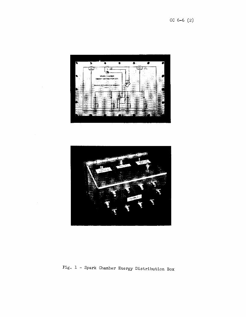
cc 6-6 (2)
Fig. 1 - Spark Chamber Energy Distribution Box
cc 6-6 (3)
II. SPECIFICATIONS A. Input Trigger Pulse.
1. Amplitude: ~ 5 kV negative. 2. Impedance: 50 Q.
3. Connector: HN.
4. Pulse Shape: a) Rise Time: ~ 10 nsec. b) Pulse width at half amplitude: ~ 20 nsec.
5. The modulator was designed to be triggered by an output pulse from the spark gap trigger amplifier (Counting Handbook CC 6-5); however, any other trigger source producing a pulse with the above charac-teristics can be used.
B. Outputs. The shape and amplitude of the output pulses are dependent on several
load and circuit parameters. For flexibility, the energy distribution box has been designed so that the main parameters can be easily changed or adjusted. Typically, the pulse rise time is 15 nsec (e.g., When, for each output connec-tor, the load is 50 Q, pulse amplitude is 10 kV, energy storage capacitor is 4000 pF, and the discharge resistor is 88 Q.)
1. Adjustable parameters: Refer to Fig. 2 for clarification of the circuit parameters. a) b)
c)
Charging voltage: External supply needed, 20 kV maximum. Spark gaps: i) Number: Two, each switches 5 outputs.
ii) Gap Spacing: Adjustable to 20 kV. Both gaps must be set for the same voltage.
t . 1 Energy s orage capacitors : 180 pF rated at 40 kV to 16,000 pF rated at 6 kV.
d) Discharge Resistors: Adjustable by plug-in units. 2. Non-adjustable Parameters: related to each output.
a) Series inductance L : 50 nHy. s b) Series resistance Rs: Mainly the spark impedance which is time
varying and is a function of the load currents. Typically, the resistance changes from an open circuit to a few ohms in about 10 nsec.
C. Delay Time. The time delay measured between the 10% amplitude points on the leading
edges of the input and the output pulses is 15 nsec. D. Repetition Rate.
0 - 40 pulses per second. The repetition rate of 40 pps is limited by the 8 msec RC recharge time constant necessary to allow the spark gaps to de-ionize when using air at 1 atmosphere.
1 See Sprague Engineering Bulletin #6311-A for an example of available capacitors. A sheet of standard ratings is printed in Fig. 7 at the end of this note.
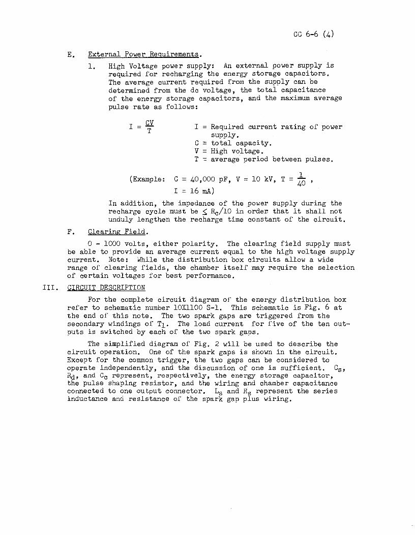
cc 6-6 (4)
E. External Power Requirements. 1. High Voltage power supply: An external power supply is
required for recharging the energy storage capacitors. The average current required from the supply can be determined from the de voltage, the total capacitance of the energy storage capacitors, and the maximum average pulse rate as follows:
I _ CV - T
(Example:
I = Required current rating of power supply.
c = total capacity. v = High voltage. T = average period between pulses.
C = 40,000 pF, V = 10 kV, T I = 16 mA)
= .1... 40 ,
In addition, the impedance of the power supply during the recharge cycle must be ~ Rc/10 in order. that it shall not unduly lengthen the recharge time constant of the circuit.
F. Clearing Field. 0 - 1000 volts, either polarity. The clearing field supply must
be able to provide an average current equal to the high voltage supply current. Note: While the distribution box circuits allow a wide range of clearing fields, the chamber itself may require the selection of certain voltages for best performance.
III. CIRCUIT DESCRIPTION For the complete circuit diagram of the energy distribution box
refer to schematic number lOXllOO S-1. This schematic is Fig. 6 at the end of this note. The two spark gaps are triggered from the secondary windings of T1. The load current for five of the ten out-puts is switched by each of the two spark gaps.
The simplified diagram of Fig. 2 will be used to describe the circuit operation. One of the spark gaps is shown in the circuit. Except for the common trigger, the two gaps can be considered to operate independently, and the discussion of one is sufficient. Cs, J\i, and Cc represent, respectively, the energy storage capacitor, the pulse shaping resistor, and the wiring and chamber capacitance connected to one output connector. Ls and Rs represent the series inductance and resistance of the spark gap plus wiring.
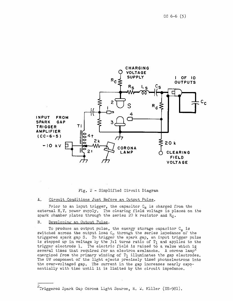
INPUT FROM SPARK GAP TRIGGER AMPLIFIER (CC-6-5)
-10 kV
Tl
CHARGING VOLTAGE SUPPLY
4
CORONA LAMP
Fig. 2 - Simplified Circuit Diagram
A. Circuit Conditions Just Before an Output Pulse.
cc 6-6 (5)
I OF 10 OUTPUTS
20 k
CLEARING FIELD
VOLTA GE
Prior to an input trigger, the capacitor Cs is charged from the external H.V. power supply. The clearing field voltage is placed on the spark chamber plates through the series 20 k resistor and Ra· B. Developing an Output Pulse.
To produce an output pulse, the energy storage capacitor Cs is switched across the output load Cc through the series impedance of the triggered spark gap S. To trigger the spark gap, an input trigger pulse is stepped up in voltage by the 3:1 turns ratio of T1 and applied to the trigger electrode 1. The electric field is raised to a value which is several times that required for an electron avalanche. A corona lamp2 energized from the primary winding of T1 illuminates the gap electrodes. The UV component of the light ejects precisely timed photoelectrons into the over-voltaged gap. The current in the gap increases nearly expo-nentially with time until it is limited by the circuit impedance, ·
2Triggered Spark Gap Corona Light Source, H. W, Miller (EE-981).
When the pulse switched across the electrodes 3 and 4. constant ~ = Ra. (Cs
cc 6-6 (6)
voltage rises across Cc, the resistor Rd is load through the spark gap consisting of
Ra. discharges the chamber voltage with a time. +Cc)•
In general, a fast rising pulse is produced which decays expo-nentially. The damping, however, is adjustable. Note that the firing of the spark chamber produces an additional transient which clips off the tail of the above exponential decay and substitutes a damped oscillation. C. Recharge Cycle.
After the output pulse is produced, the energy storage capacitors are recharged on a RC time constant determined by the total parallel capacitance of the energy storage capacitors and the series charging resistor Re. The RC time constant can be adjusted by selecting a suitable value for the series charging resistor Re. An RC time con-stant of at least 8 msec is necessary to allow sufficient time for air spark gaps to de-ionize. A longer recovery time constant is permissible providing pulse rates do not present a problem.
IV. MECHANICAL DESCRIPTION Fig. 3 (a) and (b) shows an internal view of the box in various
stages of assembly.
(a) (b)
Fig. 3 - Energy Distribution Box, Top View (a) Complete assembly. (b) View (a) with T1 , energy storage capacitors
and a pulse shaping resistor mount removed.
cc 6-6 (7)
The photograph, Fig. 3 (b) shows the pulse shaping resistors and the energy storage capacitors. To facilitate changing of values, both are fitted with "banana plug" type connections as are most of the inter-connections. One output connector is located on the bottom of the con-tainer directly under each of the energy storage capacitors. (The two spark gaps may be removed for gap setting by unplugging their connections and removing three screws from around the base of the spark gap mount. Spark gap adjustments should be made by the Counting Pool personnel in Bldg. 14.) The container has been provided with "0-ring" gaskets to make a gas-tight seal. Two LRL fittings are provided to allow some circulation of air or selected gas atmosphere. For safety reasons, when the distri-bution box is used near a hydrogen target it is necessary to flow dry filtered air at the rate of 1 to 10 cc/min. through the container. This action replaces air (or whatever atmosphere is used) which has been con-taminated by the spark gap firing. This is especially true at higher pulse rates,
At low pulse rates and away from hydrogen targets, the LRL fitting can be left open; the natural air circulation is then sufficient.
Electrical contact to preserve shielding is accomplished between the lid and the container by a ,005° ridge milled around the container flange. Care should be taken when the lid is removed not to damage this ridge.
V. OPERATION A. The Output Pulse Shape,
The output pulse shape and amplitude depend upon the circuit parameters including the spark chamber and the interconnecting cables between the pulse generator and spark chamber. Due to the current rise time in the spark gaps and the possible range of circuit parameters involved, the exact voltage wave shape across the chamber should be measured if exact information is required, The wave shape for a particular system can be estimated from circuit theory. The following comments will aid in the selection of variable parameters.
1, Cs is chosen to be several times the capacitance of Cc. This reduces the capacitive split of voltage which occurs across the spark chamber.
2. The cable connecting the generator and the spark chamber should be as short as possible to preserve a fast pulse rise time. For an electrically short length of coaxial transmission line, the inductance added per foot is given by L = Z ~ when 20 is the characteristic impedance of the line and ~ ~s the one way transit time. For one foot of RG 9/u cable L = 50 x 1. 5 x lo-9 = 75 nHy. which is comparable to the 50 nHy internal inductance of the distribution box. If necessary, several outputs from the same gap can be connected in parallel to decrease the series inductance and the rise time of the pulse.
3. To minimize spurious sparking of a chamber, the pulse voltage is made to decay exponentially by selecting a suitable discharging resistor Rct· The time constant is given by ~ = Rd (Cs + Cc) and usuaHy is from 100 to 800 nsec. (See section VI for an example of the effect of discharge time constant upon spark chamber efficiency.)
cc 6-6 (8)
B. Shielding. 1. Use double-shielded cable (RG 9/u) to connect the distri-
bution box to the spark chamber. VI. PARJUv!ETERS USEFUL WITH A TYPICAL CHAMBER.
The 4,000 pF ceramic capacitors and the 88 Q pulse shaping resis-tors supplied with the energy distribution box were found to be reason-able component values for operation with 90% neon - 10% helium filled spark chambers with the following dimensions: Plate spacing= 0.8 cm, plate areas ranged from 3'.J cm x 30 cm to 30 cm x 90 cm. Optimum chamber operation was secured when the high voltage supplied to the energy storage capacitors was between 7 kV and 9 kV. A 2 ft. 50 Q transmission line (RG 9/u)was used to connect the distribution box to the spark chamber. Fig. 4 shows the spark cha.~ber efficiency as a function of the high voltage supplied to the energy storage capaci-tors. The efficiency is plotted for the following two conditions: (1) when ionizing particles are known to have passed through the chamber plates, and (2) spurious sparking resulting when particles have not passed through the chamber. In both cases, a plot is shown for three different discharge time constants, (i.e., three different values of the pulse shaping resistor).
As an example of the use of Fig. 4, one can see that of the three time constants, ~ = 400 nsec gives the greatest latitude in H. V. gap spacing and that for ~ = 400 nsec, 7 kV/cm is a favorable choice of field.
Other chambers exhibit similar characteristics; an appropriate graph for them facilitates selection of a discharge resistor and a high voltage which will result in nearly 100% track detection efficiency while producing a negligible percentage of spurious spark-ing in the absence of tracks.
SPARK CHAMBER
EFFICIENCY (PERCENT)
0 T : 60 µsec WITH IONIZING PARTICLES
A T : 800 nsec JI
----- WITHOUI' IONIZING PARTICLES ( SPURIOUS SPARKS)
• T : 400 nsec
too
50
o+-~....q.~~f-'-~-+~~.__~-+-~~~-=;;.+.~~~~-1-~--&.~~+--~-+~~+-~-'-~----1
3 4
PLATE SPACING = o.a cm .010 in. ALUMINUM PLATES
HIGH VOLTAGE SUPPLY - kV/ cm CHAMBER SPACING
PLATE AREA = 1 ft. x 3 ft. FILLING GAS: 90% NEON 10% HELIUM
Cs= 4000 pF
GRAPH SHOWING THE EFFECT OF PULSE RC DECAY TIME CONSTANT UPON THE EFFICIENCY OF A LUCITE FRAME SPARK CHAMBER
FIGURE 4
0 0
°' I
°'

cc 6-6 (10)
VII. TYPICAL SPARK CHAMBER SYSTEM5
To emphasize the role of the energy distribution box (SCPM) in a system, a block diagram of a simplified spark-chamber system is shown in Fig. 5. Table 1 indicates the time delays that are typical of each component of the system. Counting Handbook references are indicated. All components with the exception of the spark chambers are available from the Counting Pool.
====1 DETECTOR
SPARK CHAMBER __ ____. COi N . .....__
DETECTOR i------41 DI SC.
~------- SCPM 1-------1 SG TA 1---------.....J
Fig. 5 - Simplified Spark Chambe.r System Block Diagram.
SYSTEM COMPONENT TIME DELAYS COUNTING HANDBOOK
Detectors 5-80 nsec ~· Section cc 8 Discriminator & Coincidence 2-20 nsec~~ Section cc 3 Spark Chamber Trigger Amplifier 30-40 nsec Section cc 6 Spark Chamber Pulse Modulator 10-20 nsec Section cc 6
TABLE 1
~< The shortest time delays are not- necessarily available from counting pool equipment but can be obtained with commercially available components (e.g., Minature phototubes operated at high voltage per stage and tunnel diode logic circuits.)
REFERENCE
5Q. A. Kerns, "Spark-Chamber Pulse Modulators", UCRL-10887 (June 1963)
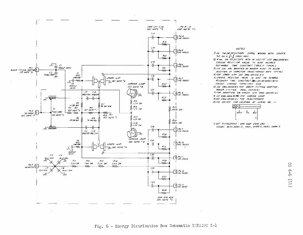
8AK£R r1rrlM6 AM~ .[{'£NOT£ '6
P6l t/6-36.J/I/
.JC[ A/drC •7
P6.1 V6·65T/t/
Tl !-<~---- •10.J CORc
fr< N07< •9
~JUl.J/..Jlr-----+-~f------j (j/ uz
100,HSKY ll!/J1f 51(V
,-fl JP4RK 6AP '-lflhfcc NOT< •4
CORONA lAAIP ..fee NOT< •4
CORONA LAMP Jc£ NOT<• 8
FOR C/3- czi Ice NOT< "J
CIJ
R/9
CIT
l pc; 4-13
JEE NOTE "'T
P6 4 (k;-560/t/
P66 f/6-560/f/
P6T t/6-S6o/v
R29 .JOO.fl 2W
RJo J00.12 lW
P6 9 '16-560/V
1'610 f/6-S60/V
.P61/ V6·360/V
P& !l L/6-560/1/
P61.J t/6-560/v
FOR Rl9·R_l8 I f<£ wore •z
NOTCf
1) i4 zu 2111 RcSIITORI SPIRAL 11101/N/) fJllTI-/ COITcR T'AP t})./ A I"' i EPOXY POST
2)4ea. 2/V RcS/3ToR3 MT/J. IN ll/CITc-fcE/JIV&!lJKJI02·11-5 Cl-/OOSC Rcf!STOR llAll/c TO &IVC PCJIRclJ OlfCl-/AR&c TIMc CONfT-4NT ( 881! II Trp1CAL)
J) Cl3·C2L AR£ Mt:JVNTCD OAI 8AAIANA PU/6.J" TO AL.LOW f€L€CTl~A/ OF CAPACITOR VALVC (""1000,Pr ftJKV Tl'/llCAl)
4)rOR JPARI( 6AP Sec /)H/6. IOl(IJOO-A--3 3) Cl-/00.ff RCS!fTOR I/AUK ro 6/Vc TllC Pc.uli'cP
RcCOl/cRY T!Mc - CONfTANT fa-.r<e.ORtlOR<) WITN £A/£R&Y .ITCJRA6€ CAPACITORS Vf£P
6) fee /)H/6.!0XllONf-6 FOR BAKcR FITT!N6 A/JAP/OR: 8AK£.e F/TT/A./6 PW&. /OAZ041
r) rtJR .Wt:JP/F/C~ t/6 -~60/u S[£ OJV6. /OK/IS2·A-I
8) f<E" CU&. NOT£ EE-?81 roR CORONA LAUP 9)..fcc PU/6 IOX/100-A-I FOR TRAl./JFORMcR
IO) fee fKc TCH roR LOCATION or fcRIAl Ala -
0 0 0 "4AK£R" "HJ..r •INC#
0
!J f<< Ph'OT06RAP#I : 5P.t"'. 4AP Z910, ;911 : 4SI'1Y. ~479, Z""140·C, 2~41, 2482·C, 244..f, 2464·C
Fig. 6 - Energy Distribution Box Schematic lOXllOO S-1
0 0
°' I
°'
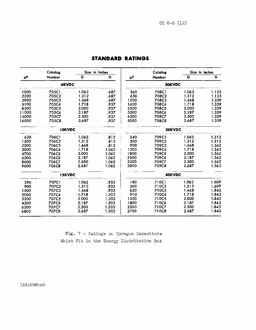
cc 6-6 (12)
STANDARD RATINGS
Catalog Size in Inches Catalog pf Number D H pf Number
6KVDC 20KVDC ~· ·-------- ---
1000 705C1 1.062 .687 360 708C1 2200 705C2 1.312 .687 650 708C2 3900 705C3 1.468 .687 1200 708C3 5100 705C4 1.718 .937 1600 708C4 8200 705C5 2.000 .937 2500 708C5
11000 705C6 2.187 .937 3300 708C6 15000 705C7 2.500 .937 4300 708C7 16000 705C8 2.687 .937 5000 708C8 ------ ---·- ----------
lOKVDC 30KVDC ---------- - --------------·--- -----
620 706C1 1.062 .812 240 709C1 1200 706C2 1.312 .812 500 709C2 2200 706C3 1.468 .812 900 709C3 3000 706C4 1.718 1.062 1200 709C4 4700 706C5 2.000 1.062 1800 709C5 6200 706C6 2.187 1.062 2500 709C6 8600 706C7 2.500 1,062 3300 709C7 9600 706C8 2.687 1.062 3900 709C8
------------- -------------- ---------- -------15KVDC 40KVDC
-~-·-·------ -- -- - ----------~-
390 707C1 1.062 .953 180 710C1 900 707C2 1.312 .953 360 710C2
1500 707C3 1.468 .953 620 710C3 2000 707C4 1.718 1.203 910 710C4 3300 707C5 2.000 1.203 1300 710C5 4300 707C6 2.187 1.203 1800 710C6 6200 707C7 2.500 1.203 2500 710C7 6800 707C8 2.687 1.203 2700 710C8
Fig. 7 - Ratings on Sprague Capacitors Which Fit in the Energy Distribution Box
QAK:HWM:mt
Size in lpches D H
1.062 1.125 1.312 1.125 1.468 1.359 1.718 1.359 2.000 1.359 2.187 1.359 2.500 1.359 2.687 1.359
--------1.062 1.312 1.312 1.312 1.468 1.562 1.718 1.562 2.000 1.562 2.187 1.562 2.500 1.562 2.687 1.562
1.062 1.609 1.312 1.609 1.468 1.843 1.718 1.843 2.000 1.843 2.187 1.843 2.500 1.843 2.687 1.843

File No. CC 6-7 (1) Q. A. Kerns A. K. Wolverton February 10, 1964
Lawrence Radiation Laboratory, University of California, Berkeley
COUNTING NOTE
A HIGH-VOLTAGE PROBE FOR NANOSECOND PULSES I. INTRODUCTION
This note describes a 'Wide-band oscilloscope probe developed for monitoring the waveforms of high-voltage nanosecond pulse modulators such as spark-chamber drivers and Kerr-cell shutters. The probe meets three design objectives. The initial goal was a voltage attenuating device that would put a minim.um load on the voltage source and deliver an output voltage to a 50 ohm transmission line. This 50 ohm output voltage amplitude also had to be sufficient for a 'Wide-band oscilloscope like the Tektronix 519 (about 10 volts/cm deflection sensitivity), either directly or through 'Wide-band 50 ohm attenuators.* The third objective was to optimize the probe band 'Width to utilize as much of the band 'Width of these oscilloscopes as possible,
These requirements led to the development of a series of high impedance, compensated probes for 20, 40, and 80 kV. The output, matched to a 50 ohm coaxial line through a type N connector, has a rise time of less than 0.5 nseo. Furthermore, the probe has do response; there is no droop imposed on a flattop pulse.
II. INPUT IMPEDANCE Units can be made 'With various input resistances and voltage division
ratios under the constraint that for a 50 ohm output: (input resistance) = 50 x (voltage division ratio)
For example, a division ratio of 200:1 sets input R at 10 k. The voltage division ratios were selected to make the probe usable over a 'Wide range of input voltages in conjunction with the Tektronix 519, whose sensitivity is approximately 10 volts/om. For instance, with a 200:1 probe used directly, 2 kV input to the probe will give 1 om deflection. This enables the user to view small details on larger peak amplitude waveforms. To view a larger pulse 'With the same probe, one simply inserts a suitable number of 50 ohm attenuators (such as General Radio 874-G) in the outp.it coaxial line.
*
The input shunt capacitance of the probe is as follows:
MODEL 20 kV 40 kV 80 kV
INPUT C
1.5 pF 3 pF 6 pF
For example, General Radio 874-G attenuators.
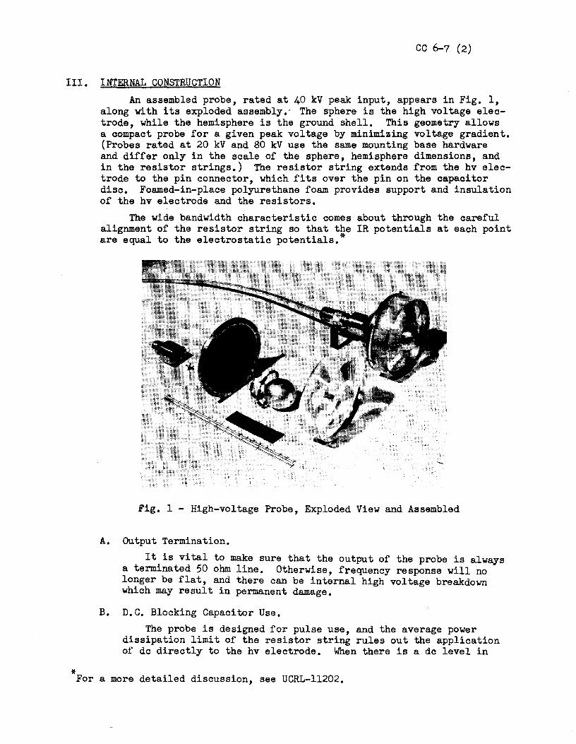
cc 6-7 (2)
III. INTERNAL CONSTRUCTION
*
An assembled probe, rated at 40 kV peak input, appears in Fig. 1, along with its exploded assembly.- The sphere is the high voltage elec-trode, while the hemisphere is the ground shell. This geometry allows a compact probe for a given peak voltage by minimizing voltage gradient. (Probes rated at 20 kV and 80 kV use the same mounting base hardware and differ only in the scale of the sphere, hemisphere dimensions, and in the resistor strings.) The resistor string extends from the hv elec-trode to the pin connector, which fits over the pin on the capacitor disc. Foamed-in-place polyurethane foam provides support and insulation of the hv electrode and the resistors.
The wide bandwidth characteristic comes about through the careful alignment of the resistor string so that the IR potentials at each point . * are equal to the electrostatic potentials.
Fig. 1 - High-voltage Probe, Exploded View and Assembled
A. Output Termination. It is vital to make sure that the output of the probe is always
a terminated 50 ohm line. Otherwise, frequency response will no longer be flat, and there can be internal high voltage breakdown which may result in permanent damage.
B. D.C. Blocking Capacitor Use. The probe is designed for pulse use, and the average power
dissipation limit of the resistor string rules out the application of de directly to the hv electrode. When there is a de level in
For a more detailed discussion, see UCRL-11202.
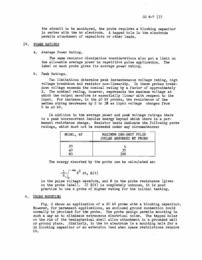
cc 6-7 (3)
the circuit to be monitored, the probe requires a blocking capacitor in series with the hv electrode. A tapped hole in the electrode permits attachment of capacitors or other leads.
IV. POWER RATINGS
A. Average Power Rating. The same resistor dissipation considerations also put a limit on
the allowable average power in repetitive pulse application. The label on each probe gives its average power rating.
B. Peak Ratings. Two limitations determine peak instantaneous voltage rating, high
voltage breakdown and resistor non-linearity. In these probes break-down voltage exceeds the nominal rating by a factor of approximately 2. The nominal rating, however, represents the maximum voltage at which the output waveform is essentially linear with respect to the input. For instance, in the 40 kV probes, the resistance of the series string decreases by 2 to 3% as input voltage changes from 0 to 40 kV.
In addition to the average power and peak voltage ratings there is a peak nonrecurrent impulse energy beyond which there is a per-manent resistance change. Resistor tests indicate the following probe ratings, which must not be exceeded under any circumstances:
MODEL, kV MAXIMUM ONE-SHOT PULSE JOULES ABSORBED BY PROBE
20 4 40 35 80 300
The energy absorbed by the probe can be calculated as:
~i GO E2 dt, E(t)
0 is the pulse voltage waveform, and R is the probe resistance (given on the probe label). If E(t) is completely unknown, it is good practice to use a probe of higher rating for the initial testing.
V. PROBE MOUNTING
Fig. 2 shows an application of a 20 kV probe with a blocking capacitor. However, for permanent applications, an enclosed ground connection could normally be provided for the probe. The probe design permits mounting in such a way as to eliminate extraneous electrical noise. The tapped holes on the rim of the hemispherical shell allow attachment to a grounded wall or ground plane. Similarly, in the hv electrode is a mounting hole for a de blocking capacitor or an extension lead when space restrictions require it.
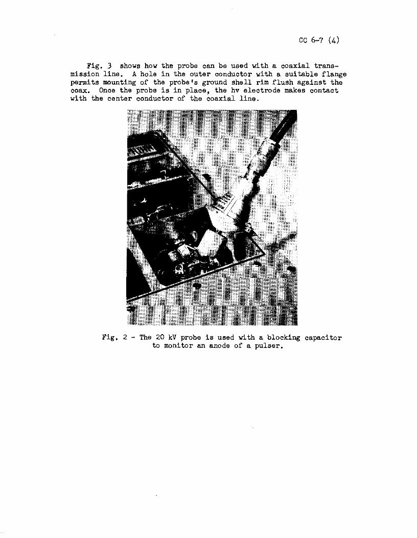
cc 6-7 (4)
Fig. 3 shows how the probe can be used with a coaxial trans-mission line. A hole in the outer conductor with a suitable flange permits mounting of the probe 1s ground shell rim flush against the coax. Once the probe is in place, the hv electrode makes contact with the center conductor of the coaxial line.
Fig. 2 - The 20 kV probe is used with a blocking capacitor to monitor an anode of a pulser.

cc 6-7 (5)
Fig. 3 - The 40 kV probe mounted in a coaxial transmission line.
QAK:AKW:mt
File No. CC 6-8 (1) G. Constantin and
C. Anderson August 10 • 1966
Lawrence Radiation Laboratory. University of California. Berkeley
COUNTING NOTE
15kV 20mA SPARK CHAMBER BOOSTER SUPPLY
I. PURPOSE
An unregulated high voltage de power s\:pply operating from regulated ac input power is often a satisfactory voltage source for spark chamber capacitor banks. The high internal impedance of available unregulated power supplies at high spark repetition rates, however, can result in a drop in output voltage.
The 15kV • 20mA power units used at the Laboratorr show a significantly varying internal impedance from no-load to full-load conditions. With the input voltage set to give an output of 15kV at 20mA, the impedance varies from 270K at 2.5mA load to 96K at 20mA load.
If a 99 percent recovery of the capacitor bank voltage is needed, it may be necessary to impose a costly dead time on the entire system. The purpose of the booster circuit is to recharge capacitor banks at a higher rate than is possible with an un-aided power supply.
II. PRINCIPLE OF OPERATION
An 80 percent recovery of a simple R-C circuit requires approximately 1.6 time constants, while a 99 percent recovery would require 4.6 time constants. The object of the booster circuit is to immediately boost the ac input to the power supply by 20 to 25 percent following a spark discharge, thereby forcing the capacitor bank to charge up to the full quiescent voltage level in the time normally required to charge up to the 80 percent level. In practice the power supply is used to recharge spark chamber capacitors through current limiting resistors of sufficient value to allow the sparks to quench. Since the power supply contains stored energy in the filter capacitors, the voltage drop seen at its output is often less than the nearly 100 percent drop on the capacitor side of the current limiting resistor during a spark. Therefore, the boost is effectively much greater than the 20 to 25 percent voltage rise would seem to indicate. As seen in the comparisons shown in Table I, the improvement in recovery time can be close to a factor of 10. The times listed are for recovery within 1 percent of the initial value.
cc 6-8 (2)
III. THE CIRCUIT
The ac input to the power supply is dynamically stepped by means of a switchable series impedance element. The impedance element is a two-winding reactor. The impedance of the primary is controlled by switching the load on the secondary winding between short circuit and open circuit; thereby switching the primary impedance from nearly zero to L , the mag-netizing inductance of the control transformer. During the q~iescent intervals between capacitor recharge, when there is little or no output load, sufficient reduction in input voltage to the H-V power supply is ensured by an extra load following the series impedance. Manual adjustment of output high voltage is made by means of a variable transformer during the quiescent period.
A resistive divider (the high-voltage meter series resistance) is used to sample the high-voltage output. Silicon controlled recitifiers between the center tap and each half of the control transformer secondary are fired by this control voltage to effectively reduce the reactor imped-ance to a low value during the boost cycle, thereby providing full line voltage to the variable-transformer input for boost action.
IV. OPERATING INSTRUCTIONS
An auxiliary meter on the front panel of the power supply indicates the control current to the SCR gate. The adjacent adjustment control should be in the extreme counter-clockwise position while setting the high voltage. Once the main-voltage control (the variable transformer setting) has been set to deliver the desired voltage to the capacitor bank, the auxiliary control should be adjusted to bring the meter pointer just to the red line. The high-voltage meter will be seen to rise as this control is rotated further clockwise. This is caused by the boosting circuit cycling periodically.
Since the boost varies by half-cycle increments at the power-line frequency, the control accuracy is thereby limited to approximately 1 percent.
Line.voltage regulation ahead of the supply is highly recommended since none is built in.
GC/mlr
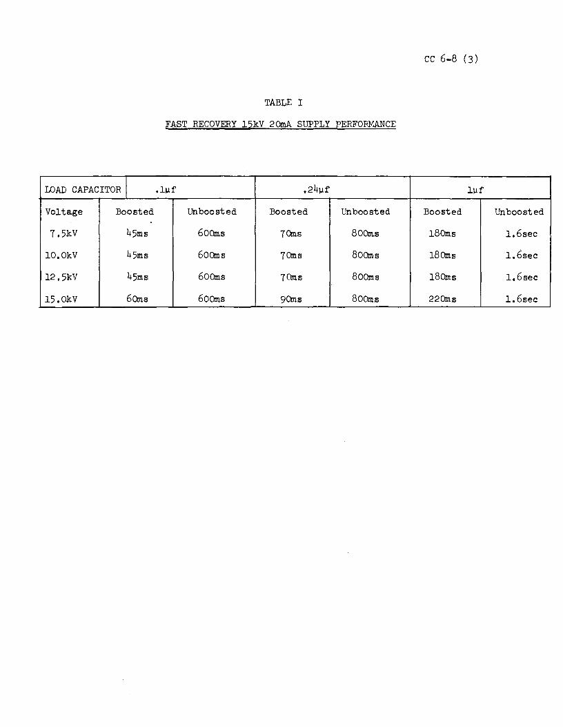
cc 6-8 (3)
TABLE I
FAST RECOVERY 15kV 20mA SUPPLY PERFORMANCE
LOAD CAPACITOR I .lµf .24µf lµf
Voltage Boosted Un boosted Boosted Un boosted Boosted Un boosted . 7 ,5kV 45ms 600ms 70ms 800ms 180ms l.6sec
10,0kV 45ms 600ms 70ms 800ms 180ms l.6sec
12. 5kV 45ms 600ms 70ms 800ms 180ms l.6sec
15.0kV 60ms 600ms 90ms 800ms 220ms l.6sec
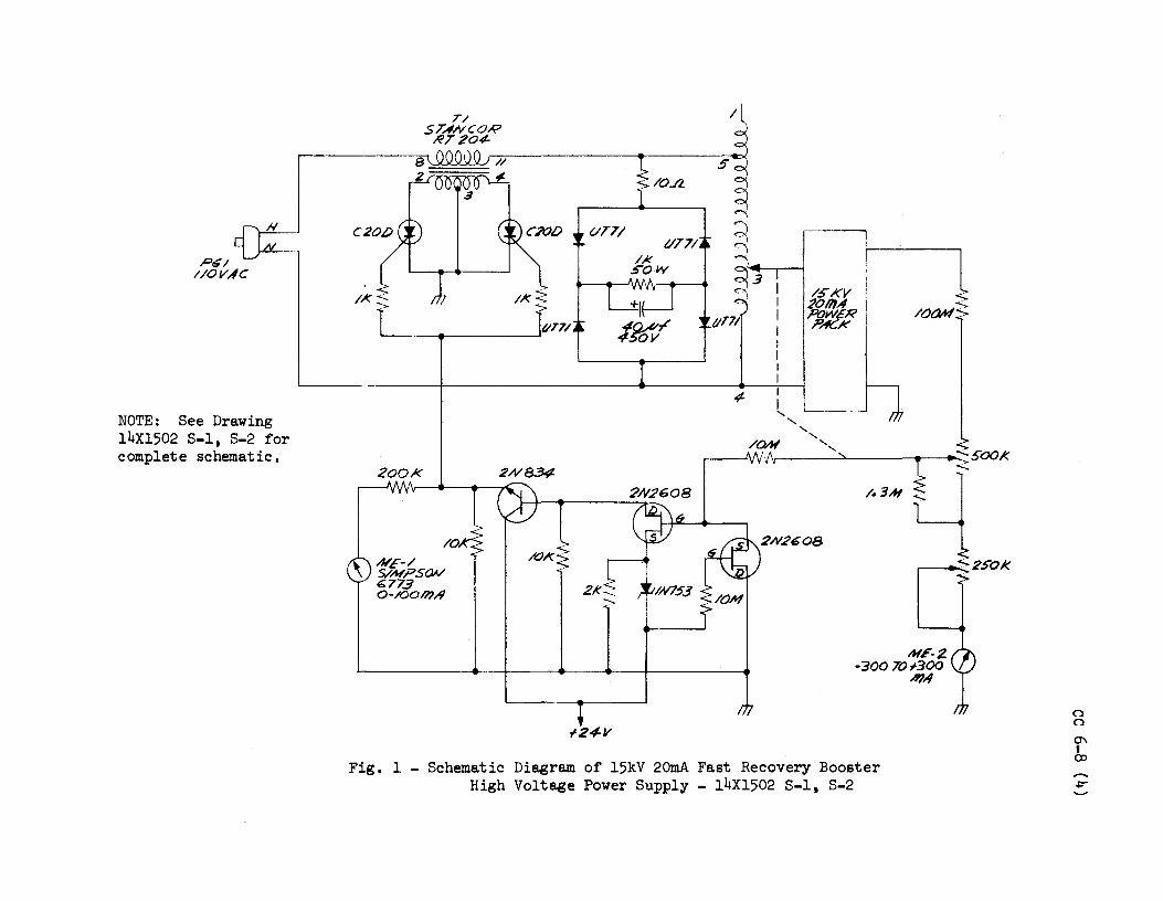
P~I l/OV,/C
NOTE: See Drawing 14Xl502 S-1, S-2 for complete schematic,
200K
Tl ST.l'INCOR
.RT 204-
NE-/ S/NPSCW 6773 o-/OomA
/0.A.
t1T7.
I I ' '
/5KV 11 20/hA I "'-,. POWER 1 /OOM ?ACK
/ON '....._,, ---"". /\ '
.______________ -------*-----+-----____. ME-2
-300 TOt-300 /11"9
Fig, 1 - Schematic Diagram of 15kV 20mA Fast Recovery Booster High Voltage Power Supply - 14Xl502 S-1, S-2
0 0
O'\ I
°'

File No. CC 8-2C (1) D. Mack Rev. December 21, 1964 D. A. Mack, M. Thibideau
Lawrence Radiation Laboratory, University of California, Berkeley
CQUN'l'ING,.NOTE
MULIIPLIER PHOTOTUBE - MANUFACTURER'S DATA
ABSTRACT A survey has been made of the multiplier phototubes suitable for scintJll-
ation and Cerenkov counting generally available in this·'cquntry including the characteristics of most interest to the experimenter. Many other photo-sensitivs devices which may occasionally be used for scintillation counting have not been listed, The quantum efficiency was calculated from manufacturers' data; all other items were compiled from manufacturers' information. 1,2,3,4,5,6,7,8. PHOTOTUBE TYPES
Phototubes with 3 or 4 digit designation numbers (e.g. 7046), issued by the Joint Electron Devices Engineering Council (JEDEC), are in commercial pro-duction in the U,S,A« Developmental and specialized phototubes produced by DuMont-are designated by the letter "K" followed by four digits. The RCA Lancaster, Pennsylvania plant identifies its developmental tubes with a letter "C 11 followed by 4 or 5 digits. CBS developmental tubes are listed as "CL1' followed by 4 digits. Westirighouse developmental tubes are identified with letters 11WX 11 , Developmental tubes are not in high quantity production, the electrical characteristics are subject to change, and usually no guarantee is made a~ to future availability. CATHODE QUANTUM EFFICIENCY
The cathode quantum efficiency, the ratio of emitted photoelectrons to incident photons, as defined here includes the transmissionandreflection losses of the window and thus becomes a value for the tube and not the photosurface alone.9, The quantum efficiency is given for the wavelength of maximum response, i.e., the spectral region of greatest photosensitivity. Quantum effictency has been calculated as the product of the cathode radiant sensitivity in microamperes per microwatt and the photon energy in electron volts for the.wavelength of maximum response. PULSE RISE TIME
Two figures are often given by the manufacturer: measured between 10% and 90% of maximum anode signal. by transit time variations in the multiplier and with (e.g. 1 mm) centered on the photocathode,
Anode pul~e rise time is It is determined primarily
a small incident light spot
Cathode transit time difference for a certain specified area of the cathode is the transit time for light pulses striking that area minus the transit time for light pulses striking a reference a+ea (center) of th~ cathode,
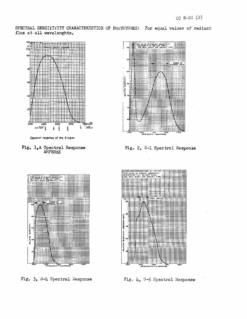
CC 8-2C (2)
SPECTRAL SENSITIVITY CHARACTERISTICS OF PhUTOTUBES: flux at all wavelenghts.
For equal values of radiant
120
Rllativt $ptttral rts
100
80
40-Spectral response of the A-types.
Fig. l,A Spectral Response AMPEREX
F'DR VALUE Of',RADIANT SENSITIVITY ~A/JjWATT) AT 100-UNIT POINT, SEE DATA SHEET FOR SPECIFIC TYPE.
100
eo
60
20
0 3000
RANGE OF MAXIMUM VALUE
~000 7000 9000 WAVELENGTH-ANGSTROMS
11000
Fig. 3, S-4 Spectral Response
140
120
100
eo
60
40
20
RANGE OF MAXIMUM VALUE
!1000 7000 9000 11000 WAVELENGTH- ANGSTROMS
Fig. 2, S-1 Spectral Response
FOR VALUE OF RADIANT SENSITIVITY ~AMP/~WATT) AT 100-UNIT POINT, SEE DATA SHEET FOR SPECIFIC TYF'E
100
1000
RANGE or MAX. VALU
3000 5000 7000 WAVELENGTH-ANGSTROMS
9000
Fig. 4, S-5 Spectral Response
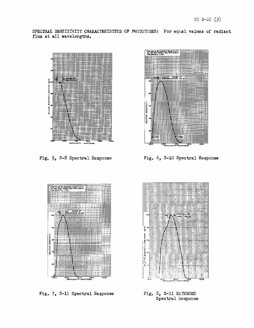
CC 8-2C (3)
SPECTRAL SENSITIVITY CHARA.C'IERISTICS OF PHOTOTUBES: flux at all wavelengths.
For equal values of radiant
"o
eo
•o
WAVELENGTH - ANGSTROMS
Fig. 5, S-8 Spectral Response
Fig.
FOR VALUE OF RADIANT SENSITIVITY AT IOO-UNIT POINT, SEE DATA SHEET FOR SPECIFIC TYPE.
RANGE DF MAXIMUM VALUE
100
80
00
40
20
0 3000 5000 7000 9000
WAVELENGTH-ANGSTROMS
7, S-11 Spectral
11000
Response
f'OR VALUE OF' RADIANT SENSITIVITY AT 100-UNIT POINT, SEE DATA SHEET f'OR SPECIFIC TYPE.
100
zo
0 3000
3200 tl50
RANGE OF MAXIMUM VALUE
5000 7000 9000 WAVELENGTH-ANGSTROMS
11000
Fig. 6, S-10 Spectral Response
I ttt~iTMtMtttttTtttHIMlrtHrt+l!itiii
100.
Fig. 8, S-11 EXTENDED Spectral Response
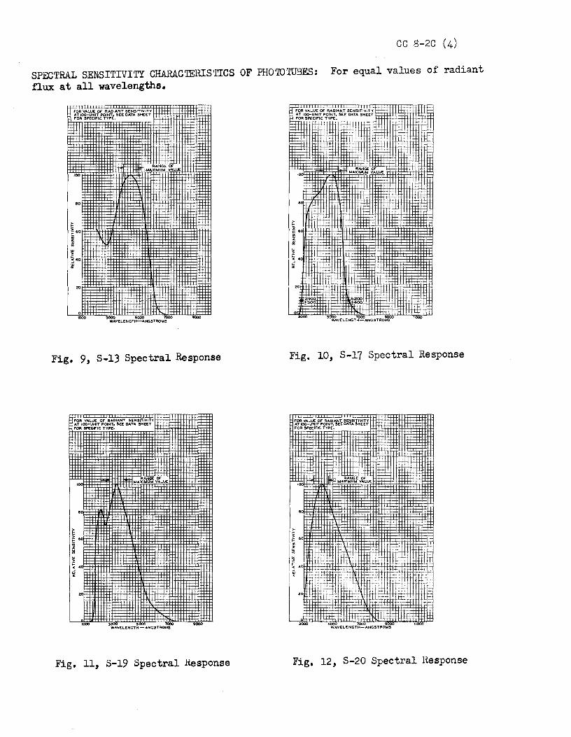
CC 8-2C (4)
SPECTRAL SENSITIVITY CHARA.C'l'ERISTICS OF PHO'IOTUBES: flux at all wavelengths.
For equal values of radiant
FOR VALUE OF RADIANT SENSITIVITY ~~ogp~~iVir?'~iJ"E.SEE CATA SHEET
RANGE OF MAXIMUM VALUE
100
80
60
40
20
0 1000 3000 5000 7000 9000
WAVELENGTH-ANGSTROMS
Fig. 9, S-13 Spectral Response
l'OR VALUE OF RADIANT SENSITIVITY AT 100-UNIT POINT, SEE DATA SHEET l'OR SPEc;.lrlC TYPE·
IOO
••
••
1000
RANGC Of" MAXIMUM VALUE:
3 5000 7000 WAVELENGTH- ANG.STROMS
Fig. 11, S-19 Spectral Response
FOR VALUE OF RADIANT SENSITIVITY AT 100 UNIT POINT, SEE DATA SHEET FOR SPECIFIC TYPE.
RAN GE or MAXlMU M VALUE
80
•o
is! ~ 40
20
100()
Fig. 10, S-17 Spectral Response
FOR VALUE OF RADIANT SENSITIVITY AT 100-UNIT POINT, SEE: DATA SHE:E:T FOR SPEClnc TYPE:.
100
. .
3000
RANGE: Of MA.XIMUM VALUE
5000 7000 9000 WAVE:LENGTH-ANGSTROMS
11000
Fig. 12, S-20 Spectral H.esponse
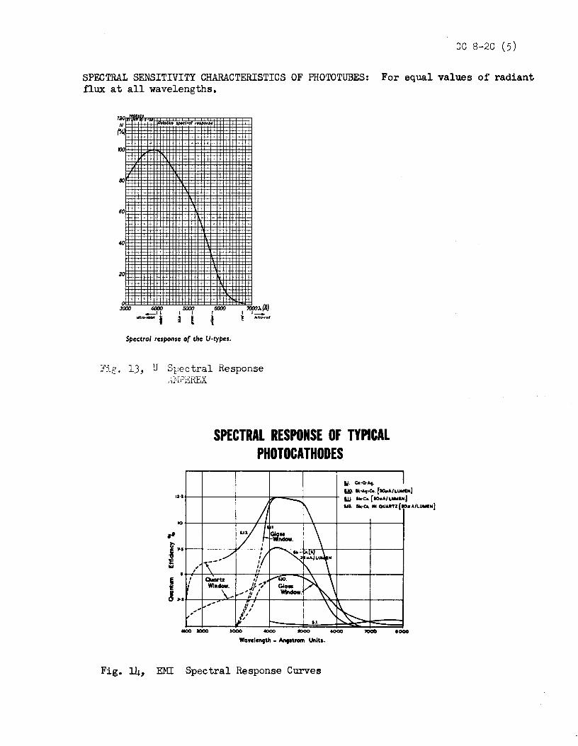
'.JC 8-2C (5)
SPECTRAL SENSITIVITY CHARACTERISTICS OF PHOTOTUBES: For equal values of radiant. flux at all wavelengths.
,. (°!.
100
lJO
60
20·-Jlx,o 4000 sooo 6000 mo~ (A)
,.__I I I I I I I ___.., "1,..._,., I I l l l infro..,•-
Spectra/ response af the U-types.
Fis. 13, U S1Jec tral Response .the EH.EX
SPECTRAL RESPONSE OF TYPICAL PHOTOCATHODES
!!· c.,a-.,. '9· IHt..C.. (-A/LUMINJ
12·1t--j----t-----t.l-o;;;;;;:=-t----t- W '°'C1. (IO•A/LUMINj IJI. 9'·~ IN QUAaTI (IO•A/LU .. Nj
IO ,.. f,.. 'O : "' , ,
I , ,
I
~ ...
S.I.
1000 IOOO 6000 1000
Wavelength - Anptrom Utlita.
Fig. 14, EMI Spectral Response Cll!I'Ves
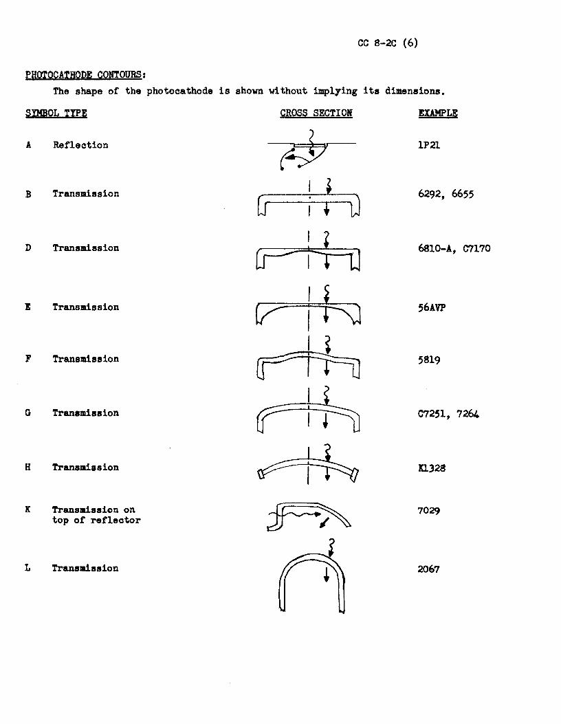
CC 8-2C (6)
PHOTOCATHODE CONTOURS: The shape of the photocathode is shown without impl7ing its dimensions.
SIMBOL TypE CROSS SECTION EXAMPLE
A Reflection 1P21
B Transmission 6292, 6655
D Transmission 6810-A, C7170
E Transmission 56AVP
, Transmission 5819
G Transmission C7251, 7264
H Transmission I ll.328
K Transmission on
~ 7029 top of reflector
L Transmission 2067
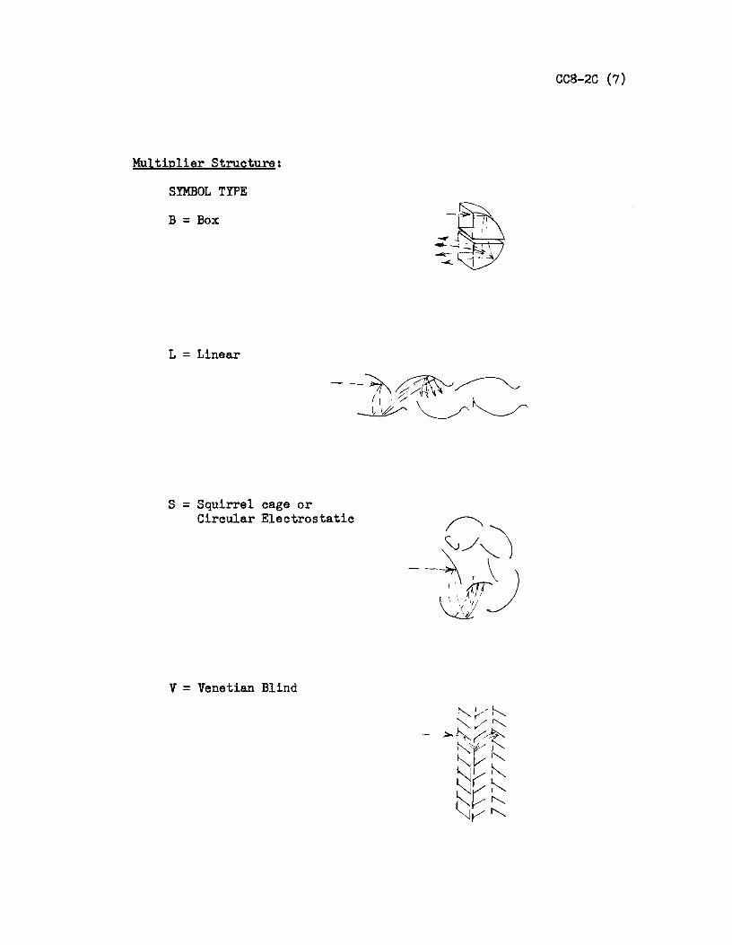
Multiplier Structure:
SYMBOL TYPE
B = Box
L = Linear
S = Squirrel cage or Circular Electrostatic
V = Venetian Blind
CC8-2C (7)
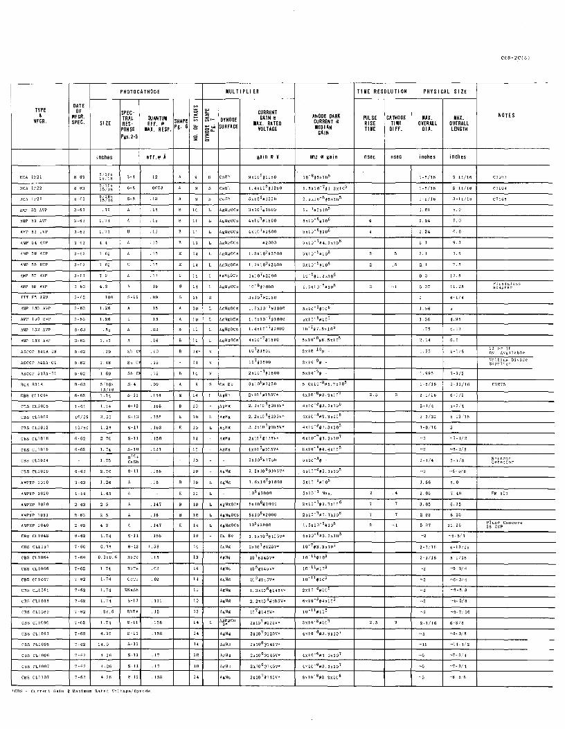
TYPE &
MFGR.
RCA 1P21
RCA 1P22
RCA 1P28
AMP 52 AVP
AMP 53 AVP
AMP 53 UVP
AMP 54 AVP
A~lP 56 AVP
AMP 56 UVP
AMP 57 AVP
AMP 58 AVP
ITT Fii' 129
AMP 150 AVP
AMP 150 UVP
AMP 152 AVP
AMP 153 AVP
ASCOP 541A-08
ASCOP 542A-01
ASCOP 543A-01
R.CA 931A
CBS CLl 004
CBS CL1008
CBS CL1009
CBS CL1012
CBS CL1016
CBS CL1018
CBS CL1024
CBS CL1029
AMPXP 1010
AMPXP 1020
AMPXP 1030
AMPXP 1031
AMPXP 1040
CBS CLl 048
CBS CL1050
CBS CL1064
CBS CL1066
CBS CLl 067
CBS CL1081
CBS CL1 088
CBS CL1089
CBS CL1090
CBS CL1093
CBS CLl 095
CBS CLl 096
CBS CL1097
CBS CLl 107
OATE OF
MFGR. SPEC.
8-63
8-63
8-63
3-63
3-63
3-63
3-63
3-63
3-63
5-62
3-63
3-63
3-63
3-63
5-62
5-62
5-62
B-63
6 - 62
1-61
10/59
10/59
6-62
6-62
6-62
3-63
1-64
2-63
2-63
2-63
6-62
7-60
7-60
7-62
7-62
7-62
7-62
7-62
7-62
7-62
7-62
7-62
7-62
7-62
SIZE
inches
5/ 16x 15/16
5/16x 15/16
5/16x 15/16
. 79
1.73
1.73
4.4
1. 65
1. 65
7. 9
4.3
. 100
1.26
1.26
.55
1.73
. 39
1.46
1. 69
5/16x 15116 1. 74
1. 74
2. 50
1.25
2. 70
1. 74
1. 75
2. 70
1.26
1. 65
2.5
2.5
4.3
1. 74
0. 75
0. 3x0. 6
1. 74
1. 74
1. 74
3x.6
1. 7 4
4. 36
14. 0
4.36
4. 36
4. 36
PHOTOCATHOOE
SPEC-TRAL RES·
PON SE Pgs.2-5
S-4
6-8
S-5
S-11
Sb Cf
Sb Cf
Sb CE
S-4
S-11
S-13
S-13
S-11
S-11
S-10
BlO+ Cs Sb
S-11
S-11
S-13
Rb Te
RbTe
Ce Te
KNaSb
S-13
RbTe
S-11
S-11
S-11
S-11
S-11
S-11
~ w "'
~~~~T~I SHAPE E; MAX. RESP. Pg. ~
•ff.@ l
. 12
0078
18
15 10
. 15 11
. 15 11
. 15
15
. 15 14
13
. 15
. 09 16
. 15 10
. 15 10
. 88 10
. 16
. 10 14'
. 15 14
. 15 14
09
158
. 15B 10
.158 10
.158 10
.158
. 127 10
10
. 158 10
. 15 10
. 147 10
. 16 10
. 147
. 158 10
1.58 14
15 13
. 02 14
. 02
10
.131 10
.15
. 158 14
. 158 14
14
. 17 10
.17 lO
. 158 14
*CBS Current Gain @Maximum Rated Voltage/O:ynode.
w ... ...
MULTIPLIER
ili ~ DY NOOE CURRENT GAIN@
IAX. RATEO VOLTAGE ~ b. SURFACE
~~
gain @ V
CsSb
CsSb
c~sb
AgMgOCs
AgMgOCs
AgMgOCs
AgMgOCs @2000
AgMgOCs
Ag~gOCs
AgMgOCs 3xl o7112soo
AgMgOCs
AgMgOCs
AgMgOCs
AgMgOCs
AgMgOCs
Cs Sb
AgMg 2x10 i025V*
AgMg 2. 2x10 5 @105V*
AgMg 2. 2x10 5 @105V*
AgMg 2. 2x10 5 @105V*
AgMg 2x 10 7 @125V*
AgMg
AgMg 2. 2x10 5 @105V*
AgMg
AgMgOCs 6x 10 6@2000
AgMgOCs sx106 nooo
AgMgOCs
Cu Be
AgMg
AgMg
AgMg
AgMg
AgMg
Ag Mg
AgMg
AgMgCu Be
AgMg
AgMg
AgMg
AgMg
AgMg
2x10 7 @125V*
10 7 @145V*
10 5 @145V*
1. 3x10 6 @145V*
2. 2x 10 5 @10 5V*
10 7 @145V*
2xl07 @125V*
2xl0 6 @145V*
2x10 7 @145V*
ANODE DARK CURRENT @ IEOI AN
GAIN
amp @ gain
5xI0- 3 Max.
TIME RESOLUTION
PULSE RISE Tl ME
nsec
2. 5
2. 5
CATHOOE TIME
DI FF.
nsec
.5
~1
.4
PHYSICAL SIZE
MAX. OVERALL
01 A.
inches
1-5/16
1-5/16
1-5/16
1. 01
2. 24
2. 24
5. 1
2.1
2.1
9.3
5.37
1. 56
L56
.75
2. 14
1.25
1. 995
1-5/16
2-1/16
2-1/4
3-3/32
1-9/16
2-1/4
~3
1. 56
2. 05
3. 05
2. 93
5. 37
2-1/16
2-1/16
2-1/16
~5
~5
MAX. OVERALL LENGTH
inches
3-11/16
3-11/16
3-11/16
5. 9
6. 0
6. 0
9. 3
7.5
7. 5
12.8
11. 25
4. 96
4.13
6.0
5-1/8
7-1/2
3-11/16
6-1/2
5-3/4
6-13/16
-7- 1/2
-5-3/8
5-7 /8
-6- 5/8
5.0
7. 40
6. 25
6. 25
11. 25
-5- 5/8
6-13/16
5- 9/16
-6- 3/ 4
-6- 3/ 4
-5-5/8
-5- 5/8
-5-7/ 16
6-3/8
-8- 5/8
-14-1/2
-7-3/4
-7- 3/ 4
-8-5/8
CC8-2C(8)
NOTES
C7073
C7104
C7045
Plexiglass adapter
12 or 18 O:y. Available
Vol tagp Divide Supp 1 i ed
C7075
Neutron Detector
PM 507
Plane Concave 58 AVP
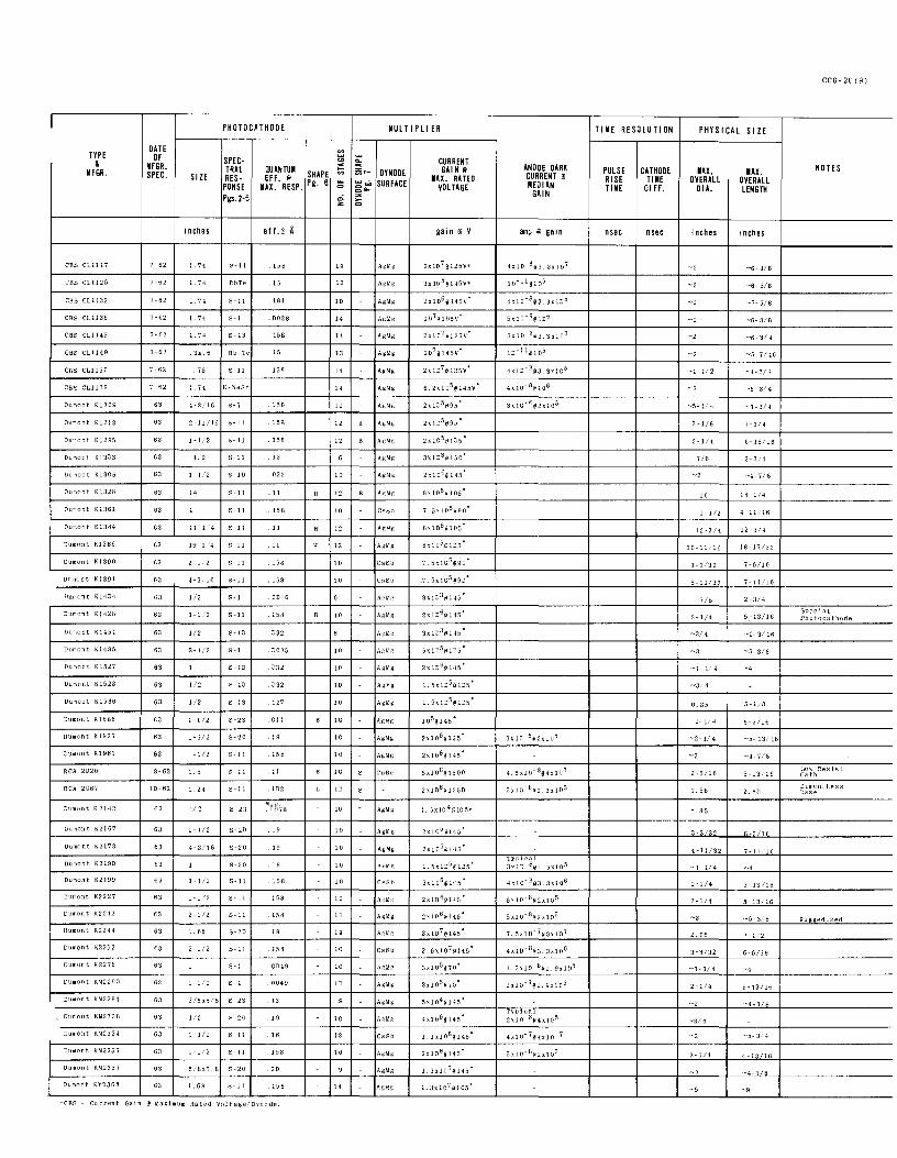
I TYPE
& MFSR.
CBS CL1117
CBS CL1125
CBS CLl 132
CBS CL1136
CBS CLl 145
CBS CL1149
CBS CLIISO
CBS CL1158
Dumont Kl209
Dumont Kl213
Duman t Kl295
Dumont KI3D3
Duman t Kl305
Dumont Kl328
Dumont Kl361
Dumont Kl384
Dumont Kl386
Dumont Kl390
Dumont Kl391
Dumont KI4D4
Dumont Kl428
Dumont Kl451
Dumont Kl485
Dumont Kl527
Dumont Kl528
Dumont Kl566
Dumont Kl6B8
Dumont Kl927
Dumont K1961
RCA 2D20
RCA 2067
Dumont K2142
Duman t K2167
Dumont K2173
Dumont K219D
Duman t K2 l 99
Dumont K2227
Duman t K2242
Dumont K2244
Dumont K2253
Duman t K2276
Dumont KM229D
Duman t KM2294
Dumont KM2328
Dumont KM2334
Dumont KM2356
Dumont KM2357
Dumont KM2368
DATE OF
MFGR. SPEC.
7-62
7-62
7-62
7-62
7-132
7-62
7-62
7-132
63
63
63
63
63
63
63
63
63
63
63
53
63
63
63
63
63
63
63
63
63
8-63
lD-62
63
63
63
63
63
63
63
63
63
63
63
63
63
63
63
PHOTO CATHODE
SIZE
inches
1.74
1. 74
1. 74
1.74
1. 74
3x. 6
.75
1. 74
SPEC· TRAL RES·
PON SE Pgs.2-5
S-11
Rb Te
S-11
S-J
S-13
Rb Te
S-11
K-NaSb
4-3/16 S-7
2-11/16 S-11
1-1 2 S-11
S-11
l-L2 S-10
14 S-11
S-11
11 l, 4 S-11
19-1 4 S-11
2-1; 2 S-11
4-3/16 S-11
1/2 S-1
1-1,'2 S-11
1/2 S- lD
2-1,2 S-1
S- lD
112 S-lD
1/2 S-13
1-1/2 S-23
1-1/2 S-20
1-112 S-11
1.5 S-11
1.24 S-11
1/2 s- 23
2-1/2 S-2D
4-3, 16 S-20
S-20
1-112 S-11
1-1!2 S-11
2- l/2 S-11
1. 68 S-2D
2-1/2 S-11
S-1
1-1/2 S-1
5/8x5/B S-23
1/2 S-20
1-1/2 S-11
1-1/2 S-11
5/8x5' 8 S-20
1.68 S-11
~~~~~· SHAPE IAX. RESP. Pg. :;
er f.@ l
158 J4
15 13
lSJ JD
. 0028 14
158 J4
15 13
158 14
14
156 12
158 12
158 J2
.13
032 IO
II 12
158 IO
II 12
II 12
158 IO
.158 JO
OD16
158 JO
D32
. D025 JO
D32 JO
D32 ID
127 JO
Oil JO
.!9 JO
158 IO
II IO
. 1D2 ID
Min. OD7B IO
.19 JD
.!9 IO
.18 IO
158 IO
158 JO
158 10
.19 14
.158 IO
OD49 IO
. 0049 ID
13
.!9 IO
16 13
158 IO
2D
158 14
*CBS Current Gain @Maximum Rated Voltage, D.ynode.
MULTIPLIER
OYNODE SURFACE
AgMg
AgMg
AgMg
AgMg
AgMg
AgMg
Ag Mg
AgMg
AgMg
Ag Mg
Cs sh
Ag Mg
AgMg
Cs Sb
Cs Sb
Ag Mg
AgMg
AgMg
AgMg
AgMg
AgMg
AgMg
AgMg
AgMg
AgMg
Cu Be
AgMg
AgMg
AgMg
AgMg
Cs Sh
AgMg
AgMg
AgMg
Cs Sb
AgMg
AgMg
AgMg
AgMg
Cs Sb
AgMg
Ag Mg
AgMg
CURRENT SAi N @
IAX. RATED VOLTAGE
gain @ V
2xlD 7 @125V*
3x lD 5 @145V*
ANODE DARK CURRENT @ MEDIAN
GAIN
amp @ gain
Typical 3x lD- 8 @1. sx10 5
Typical 2xl o- 8 ~4x 10⁵
4xl0- 7 @4xl0+ 7
TIME RESOLUTION
PULSE RISE TIME
nsec
CATHODE TllE
01 FF.
nsec
PHYSICAL SIZE
IAX. OVERALL
DI A.
inches
-1-1/2
-5-1/4
3-116
2-114
7/8
16
1-1/2
12-3/4
20-11/16
3-3/32
5-11/32
7 /B
2-1/4
-3/4
~3/4
0. 85
2-1/4
-2-1/ 4
2-5/16
1. 56
-.85
4-11/32
-1 114
2-1/4
2-1/4
2.06
3-3/32
-1-1/4
2-1/4
-3/4
2-1/4
-5
IAX. OVERALL LENS111
inches
-6- 3/8
-6- 5/8
-5-5/8
-6-3/8
-6 3/4
-5 7/ 16
-6-3/4
-7-3/4
7-1/4
6-15/16
2-3/4
-4-7/8
14-1/4
4-11/16
12-3/4
18-17/32
7-5/16
7-11/16
2-3/4
5-13/16
-2- 3/ 16
-5 3/8
5-1/8
6-3/16
-5- 13/ 16
-4-7/8
5-13116
2. 8D
7-11116
5-13/16
5-13/16
-5- 3/8
7-1/2
6-5/16
5-13/16
-4- 7/8
-5-3/4
4-13/16
CC8-2C(9)
NOTES
Special Photocathode
Low Resist. ca th.
Dimen. Less base
Rugged1zed
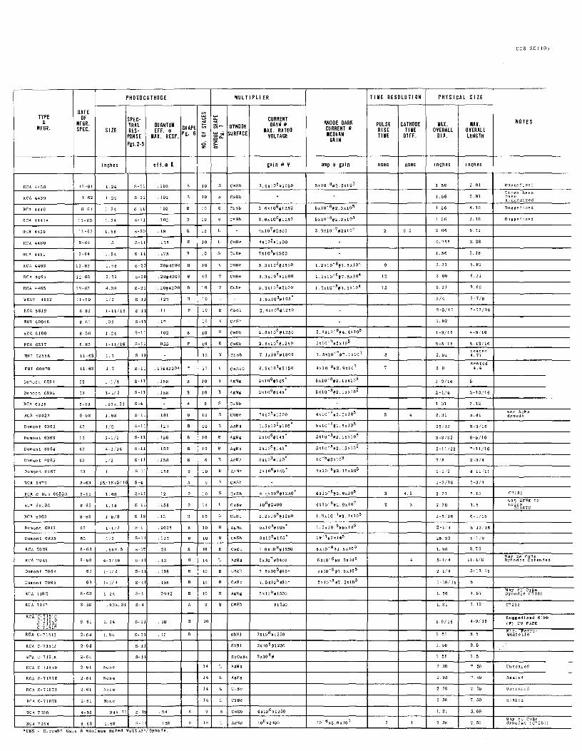
TYPE &
MFGR.
RCA 4438
RCA 4439
RCA 4440
RCA 4441A
RCA 4459
RCA 4460
RCA 4461
RCA 4463
RCA 4464
RCA 4465
\\'EST. 4582
RCA 5819
EMI 60948
RCA 6199
RCA 6217
EMI 62558
EMI 60978
Dumont 6291
oumon t 6292
RCA 6328
RCA 6342A
Dumont 6362
Duman t 6363
Dumont 6364
Duman t 6365
Oumont 6467
RCA 6472
RCA & Oum 6655A
RCA 6810A
RCA 6903
Dumont 6911
Dumont 6935
RCA 70 29
RCA 7046
Dumont 7064
Duman t 706 5
RCA 710 2
RCA 7117
RCA C- 7151C C-71510 c- 715 lE C-7151F
RCA C-71511
RCA C-7151J
RCA C-7151K
RCA C-71870
RCA C-71B7E
RCA C-7187J
RCA C-7187K
RCA 7200
RCA 7264
DATE OF
MFGR. SPEC.
12-61
1-62
8-61
11-63
11-63
2-64
2-64
12-63
12-63
12-63
11-60
8-63
8-61
8. 56
8. 63
11-63
63
8-63
9-58
63
63
63
63
63
PHOTO CATHODE
SIZE
inches
1. 24
1 24
1 24
1. 24
1. 68
1. 24
1. 68
2.59
4. 38
1/2
SPEC-TRAL RES-
PONSE Pgs.2-5
S-11
S-11
S-11
S-11
S-20
S-11
S-11
S-20
S-20
S-20
S-11
1-11/16 S-11
. 39 S-11
1. 24 8-11
elf.@ l
. 102
. 102
. 102
. 102
.19
. 175
. 175
20@4200
. 20@4200
. 20@4200
. 127
.11
17
. 102
055
1. 7 S-11 .17@4200A
1-1/4 S-11 . 158
l- 1/ 2 S-11 . 158
. 93x- 31 S-4
1. 68 S-11 .1a1
1/2 S-11 .127
2-1/2 S-11 . 158
4-3/16 S-11 .158
1/2 S-11 158
S-11 158
8-63 15/16x5/16 S-4
8-63 1. 68 S-11 .12
8-63 1. 68 S-11 . 158
8-63 1-5/8 S-13 .13
63 1-1/2 S-1 . 0025
63 1/2 S-11 .127
8-63 .65X 5 21
8-63 4-7/ 16 s- 11 .13
63 1-112 s- 11 . 158
63 1-1/ 4 s- 11 . 158
1.24 S-1 0042
3-58 . 93X. 31 8- 4
9-61 1.24 S-11 10
2-64 1.24 S- 11 .10
2-64 s- 11
2-64 s- 11
2-61 None
2-61 None
2-61 None
2-61 None
4- 58 , 94X. 31 S-1! .24
8-63 I. 68 S-1 158
*CBS - current Gain @Maximum Rated Voltage/Oynode.
10
10
10
10
12
10
10
10
10
10
10
10
10
10
10
13
11
10
10
10
10
10
10
10
10
14
10
10
10
10
14
10
10
10
10
14
14
14
14
14
MULTIPLIER
0.. ~
~~ OYNDDE ~ o0 SURFACE ~D.
cssb
cs Sb
cs Sb
cssb
cu Be
Cu Be
cu Be
cu Be
Cu Be
cs Sb
cssb
cs Sb
cs Sb
cs Sb
CsSbO
AgMg
cs Sb
Cu Be
AgMg
AgMg
Ag Mg
AgMg
AgMg
cs Sb
cs Sb
cu Be
Cs Sb
AgMg
Cs Sb
Cs Sb
AgMg
Cs Sb
Cs Sb
AgMg
cs Sb
SbNl
CURRENT GAIN @
IAX. RATED VOLTAGE
gain @ V
2x10 7 @3400
7. 5x10 5 @90*
@1250
SbNi 3x10 6 @1250
AgMg
AgMg
Cu Be
Cu Be
CsSb
AgMg 10 8 @2400
ANODE DARK CURRENT @ MEDIAN
GAIN
amp @ gain
1. 2x10⁻⁸@7. sx104
5x10⁻⁸@7. 5xlo 5
TIME RESOLUTION
PULSE RISE TIME
nsec
12
15
CATHODE TIME
DI FF.
nsec
0. 5
4.5
PHYSICAL SIZE
MAX. OVERALL
DI A.
inches
1.56
1.56
1. 56
1. 56
2. 06
0. 755
1. 56
2. 31
3. 06
5.31
3/4
2-5/16
1.92
2-5/16
2. 02
2. 0
1-9/16
2-1/4
1. 31
2. 31
25/32
3-3/32
5-11/32
7 /8
1-1/2
1-3/16
2. 31
2. 38
2-5/16
2-1/4
25/32
1.56
5-1/ 4
1-19/ 16
1.56
1.31
1-9/ 16
1.56
1. 56
1.56
2. 38
2. 38
2. 38
2.38
1.31
2. 38
MAX. OVERALL LENGTH
inches
3.91
3. 91
4.12
3.18
6. 31
3. 38
3. 18
5. 81
6.31
7. 69
3-7 /8
5-13/16
4-9/16
seated 4.77
seated 4. 4
5-13/16
3. 12
5. 81
5-3/16
6-5/16
7-11/16
2-3/4
4-11/16
2-3/4
5. 81
7.5
6-9/16
5-13/16
6-1/8
3.75
11-1/8
5-13/ 16
4.57
3.12
4-9/ 16
3.5
3.5
3.5
7. 50
7. 50
7. 50
7. 50
5. 69
7. 50
CC8-2C(l0)
NOTES
Ruggedized
Di men. Less base Rugged1zed
RuggedizPd
Ruggedized
was AgMg dynode
C7189
was AgMg dy-nodes
C7187C
May be cuse Dynodes Extended
May be CuBe Oynodes C7160
C7253
Ruggedlzed 6199 (F) UV FACE:
~in. Ferro-Magnetlc
Unsealed
Sealed
Unsealed
Sealed
May be CuBe dynodes (C7251)
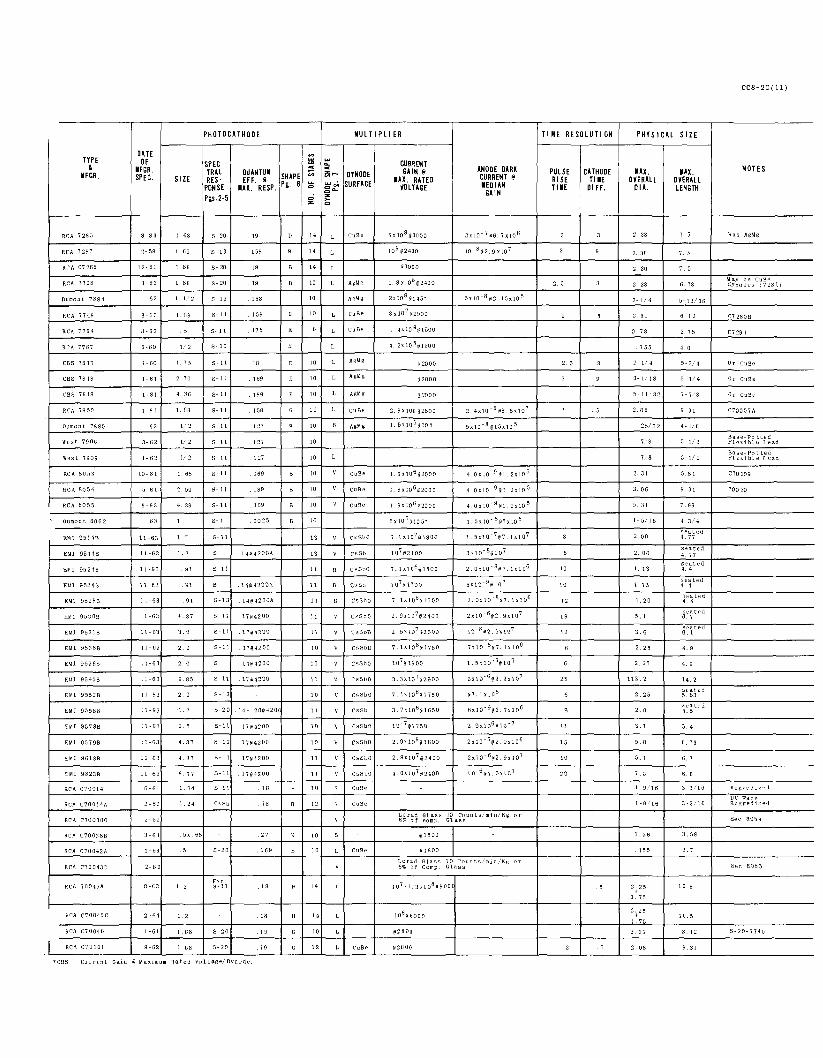
TYPE &
MFSR.
RCA 7285
RCA 7287
RCA C7268
RCA 7328
Dumont 7884
RCA 7748
RCA 7784
RCA 7787
CBS 7817
CBS 7818
CBS 7819
RCA 7850
Oumon t 7880
\\'est 7906
West 7909
RCA 80.53
RCA 8054
RCA 8055
oumont 8062
EMl 95148
EMI 95145
EMI 95248
EMI 95245
EMl 9528B
EMI 95308
EMI 95318
EMI 95388
EMI 95365
EMI 95458
EMI 95528
EMI 95588
EMI 95788
EMI 95798
EMI 96188
EMI 98238
RCA C70014
RCA C70014A
RCA C700300
RC!\ C700388
RCA C70042A
RCA C70043D
RCA 70045A
RCA C70045C
RCA C70048
DATE OF
IFSR. SPEC.
8-83
2-59
t:l-81
63
8-63
8-83
8-80
9- 60
1-61
1-81
63
3- 62
1-62
10- 81
5-61
8-83
83
11-63
11-83
11-S:J
11 63
11 63
11 63
11-63
11-63
l I-63
l l 63
11-83
11-83
11 63
11·63
11 63
11 63
6-61
2·62
2-62
3-63
I-G3
2-82
8-63
2-64
1-61
9-82
SIZE
I. 68
l. 69
l 88
1.88
I - II 2
1 68
L'2
1.75
2 70
4. 36
1 68
1 2
1"2
L 2
I 68
2. 59
4 :1s
1.7
1.7
91
. 91
4.37
3. 0
2.0
2. 0
9.85
2.0
"1.7
2 . .\
4.37
4.37
8.77
1. 24
1.24
5x.65
I.2
1.2
1.68
1. 68
PHOTOCATHOOE
SPEC· TRAL RES·
PON SE Pgs.2-5
s- 20
S-13
s- 20
s- 20
s- 13
s- 11
5- 11
s- 11
5- 11
s- 11
s- 11
s- 11
s- 11
S-11
s- 11
S-11
s- 11
S-11
S· I
S-11
S-11
19
158
19
l9
.158
158
.175
.IS
.169
189
I58
127
127
127
169
189
IGO
0025
l4@4200A
14(114200A
S-13 l4@4200A
5-11 17@4200
S-11 l 7(i4200
5- l l 17@4200
. l 7@4200
s-11 17@4200
S-13
S-20 14-. 20(0420(
S-11 17@4200
5-11 l 7@4200
S-11 l 7@4200
S-11 . l 7@4200
S-11
Cs Sb
5-20
Ext. S-11
S-20
5-20
.I8
18
27
.169
.I8
I8
. I 9
.19
14
14
14
IO
IO
IO
IO
IO
IO
12
IO
IO
IO
IO
IO
IO
IO
13
13
11
11
lI
lI
11
IO
IO
11
IO
11
10
IO
11
II
10
12
IO
IO
14
14
IO
12
MULTIPLIER
OYNOOE SURFACE
Cu Be
AgMg
AgMg
Cu Be
cu Be
AgMg
AgMg
cu Be
cu8e
Cu Be
cu Be
C,,;SbO
cssb
C~SbO
cr;Sb
CsShO
CsSbO
CsSbD
CsSbD
Cr;SbO
CsSbO
c~sbo
Cs Sb
CsSbO
Cs5b0
c~5bO
CsSbO
Cu Be
Cu BP
Cu Be
Cu8e
CURRENT SAIN @
IAX. RATED VOL TASE
2x 10 8 @3000
10 8 @2400
t s :no 8 @2400
8xI0 7 (02500
4. 2x 10 5 .~ 1500
(02000
:nooo
,'02000
2. 8Xl08@28QQ
1. Sx 10 8 ~2000
3. 3Y..10 7 @2900
7. lx.10 6 @1750
2. 9x.Io 8 @ I 800
2. 9x10 7 @2400
ANODE DARK CURRENT @ IEOI AH
SAIN
2 x 10- 7 (i6. 7 x io 6
2 4xto- 8 ros 8xto 7
5xl0- 8 @15x10 5
4. Ox.10 9 liVl 2xl0 5
Lorad Glass 10 Counts/min/Kg or 63 of comp. Glass
@1500
@1800
Lorad Glass 10 Counts/min/Kg 63 of Comp. Glass
@28Do
(<i2800
TIME RESOLUTION
PULSE RI SE TllE
2 5
2.5
IO
10
I2
18
12
25
11
1.1
10
20
CA THO OE Tl IE
DI FF.
. .\
PHYSICAL SIZE
IAX. OVERALL
DIA.
2. 38
2. 38
2 30
2 38
2-1/ 4
2.31
0. 78
755
2-1 1 4
3- L 18
5- 11/32
2. 08
25/32
7/8
7/8
2.31
3 06
5 31
1-5/18
2. 00
2. 00
1.13
Ll3
1.20
.1.1
3. 6
2.25
2.25
112. 2
2.25
2.0
3 .l
.; . 0
.I.I
7.5
1-9/16
l -9/16
1. 56
.155
3+ 25 1.75
3+25 I. 75
2.31
2. 08
MAX. OVERALL LEHSTH
7.5
7 5
7 5
6.78
5-13/18
6 12
2.75
40
5-3/4
6-1/ 4
8.31
4- 118
5- II 2
5- 11 2
.; 8I
8.31
7.89
4-3;4
seated 4.77
seated 4.77 seated 4.4
seated 4. 4
seated 4.4
seat pd 6.7
spated 6.1
4.9
4.9
14. 2 seated 5.83
i:;eated .\.5
5.4
6. 73
6.7
5. 8
3-3/16
3-3/16
3.58
3.7
10.5
10.5
8.12
8.31
CC8-2C(ll)
NOTES
\\'as AgMg
May be CuBe dYnodes ( 7 28l)
C7 280B
C729 l
Or CuBc
Or CuBe
Or CuBe
C70007A
Bast>- PO tted Flcxi ble Lead
Base-Potted E"l exibl e Lead
C70 109
70030
Rugged1zf'd
UV Facp Rui:;gedized
Sec 8054
Sec 8055
S-20-7740
I RCA C70I0l -~~~~~~--'-~~~-L-~~~~.....__,_~~~~~----'-~~~~-'--~-'-~--'~~-'-~~i.__~~~~~
*CBS Current Gain @Maximum Rated Voltage/Dynode.
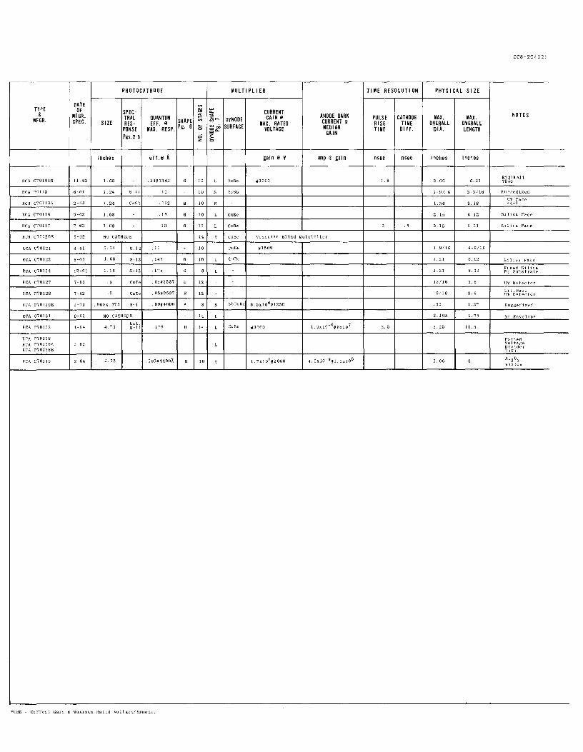
CC8-2C(!2)
PHOTOCATHOOE MULTIPLIER TIME RESOLUTION PHYSICAL SIZE
OATE ~
TYPE OF ~
CURRENT SPEC- "' Q. & MFGR. TRAL QUANTUM r;; ... GAi N @ ANODE DARK PULSE CATHODE MAX. MAX. ND TES MFGR. SPEC. SHAPE i!'i~ OYNODE CURRENT @ SIZE RES- EFF. @ MAX. RATED RISE TIME OVERALL OVERALL
PDNSE MAX. RESP. Pg. 6 ~ ~ °" SURFACE VOLTAGE MEDI AN TIME DI FF. DIA. LENGTH ="" GAIN Pgs.2-5 g ~
inches et f.@ A gain @ V amp @ gain nsec nsec inches inches
RCA C70101B 11-63 1 68 24@3342 G 12 L cu Be @3000 1. 8 2. 06 6. 31 BiAlkal i 7850
RCA 70113 6-61 l. 24 S-11 10 10 s cs Sb 1-9/1 6 3-3/16 Ru ggedizPd
UV Face RCA C70l 13A 2-62 l. 24 Cs Sb . 102 B 10 s 1.56 3.18 4441
RCA C70116 9-62 1. 68 . 18 G 10 L cu Be 2.15 6. 12 Si lie a Face
RCA C70117 7-63 1. 68 . 18 G 12 L cu Be 2 .5 2. 15 6.31 Silica Face
RCA C70120E 9-62 NO CATHODE 14 v Cu Be Venetian Blind Multiplier
RCA C70121 8-61 1.24 S. 11 . 11 10 cu Be @1500 1-9/16 4-9/16
RCA C70122 6-62 1.68 S-13 .147 G 10 L Cu Be 2.31 6. 12 Si lie a Face
RCA C70124 12-61 1.68 S-13 175 G 8 L 2.31 6.12 Fused Silica Pt. Substrate
RCA C70127 7-62 .5 Cs Te .05@2537 8 12 13/16 3.8 UV Detector
RCA C70128 7-62 .5 Cs Te . 05@2537 8 12 13/16 3. 8 Li f. Face UV OPtector
RCA C70129B 2-64 .060x.375 S-4 . 09@4000 A 8 s SbCuBe 6. 5xl0 6 @1250 . 51 1.37 Ruggedized
RCA C70131 9-62 NO CATHODF.: 14 L 3. 105 1. 75 No Envelope Ext.
RCA C70133 4-64 4.75 s-11 176 H 14 L cu Be @3000 1. 9x10- 6 @sx10 7 3.5 5. 25 10.5
RCA C70136 Potted RCA C70136A 2-62 L Voltage
01 vider RCA C70136B 7767
RCA C70145 2-64 2. 75 .183@4400X B 10 v 1.7x10⁶ @2000 4, Ox10- 9 @1. lxl0 5 3.06 8 Al 2 0 3 window
*CBS - current Gain @ Maximum Rated Voltage/Dynode.
File No. CC 8-3B (1) F. Kirsten Rev. March 5, 1964 C. Kerns Rev. May 5, 1966 C. Dumm
Lawrence Radiation Laboratory, University of California, Berkeley
COUNTING NOTE
PHOTOTUBE MEASURING TECHNIQUES
I. ABSTRACT
This note *describes the testing methods used at UCLRL to determine the suitability of multiplier phototubes for nuclear counting applications. It also explains the code in which the results of the tests are placed on each tube. These tests are performed on all newly purchased tubes of the type numbers enumerated below, as well as on tubes returned to stock.
II. TUBE MARKINGS
B c
The types of multiplier phototubes listed below are presently being tested in the way described in this note. The results of the tests are recorded on white stickers which are then placed on the keys on the bases of the tubes. The method of coding is illustrated below.
1. Tube Types
2067. 6655. 6655A, 6342A
A
2. Code Index
D B E c
CL1090, 6810A C7251, 7 26 4.
A I
24
. 77
F
7046. C-70133 7 265. 8 57 5 A
13 . 14 D 2300 3200 E c . 1 14 . 87
D E
G
H
A. UCRL serial number. This number should be referred to in requesting further information regarding the tube from Physics Technical Support, Electronics Engineering.
B. Standard gain supply voltage. The supply voltage required to obtain the standard anode-pulse current gain using the voltage dividers listed in Table I. Standard current gains: 6655A, 6342A, 2067 . . . . . . . . . . . . . . . . 2.5 x 10 5
6810A, C7251, 7 264. CL1090, 7046, 7 265 ................. 3.0 x 10 7 857 5, C-70133
C. Anode dark current (in microamps) at the Voltage of Code B. D. Maximum operating supply voltage - the voltage giving the maximum
useful gain, beyond which voltage the operating characteristics of the tube become impaired.
These methods were initially described by Bill Jackson, "Checking Multiplier Phototubes for Nuclear Counting Applications•, Engineering Note EE-494.
CC 8-3B (2)
2. (Continued) E.
F.
G.
H.
Quantum efficiency (in per cent) of the photocathode measured at a wavelength of 4200 ~.
Optimum focus electrode (Gl) voltage - the ratio VK-Gl/VK-Dl at which the maximum anode pulse amplitude is obtained with the entire cathode illuminated by a mercury-capsule light pulser. Optimum Gl voltage (7046). The ratio VK-Gl;VK-G2 at which the con-dition of Code F is fulfilled. Optimum G2 voltage (7046). The ratio VK-G2/VK-Dl at which the con-dition of Code F is fulfilled.
These quantities are described in more detail below. III. TESTING PROCEDURE
The testing methods described below were developed to test multiplier phototubes for characteristics important to counting applications. 1. Impedance Check.
A check is made for open leads and short circuits between the tube electrodes using the interelectrode impedance checker. 1 In making these short and open tests, an ac voltage whose peak value is approximately the rated interelectrode voltage is impressed in turn between each electrode and all other electrodes. This is done with the tube at rest and when it is subjected to an acceleration of about 5g.
2. Standard Gain Supply Voltage2 (Code B). The applied voltage necessary to obtain a specified pulse curren]
gain is measured. The light source is a mercury-capsule light pulser and the output current is read as the deflection of the trace on a 5XP-type CRT. The dynode voltage distributions employed in this test are listed in Table I along with the values of the pulse gain to which test results refer.
In the case of tubes for which optimum focus electrode voltages (Codes F or G and H) are listed, the standard gain supply voltage is measured with the focus electrodes set at these voltages.
The light pulses are short enough so that after pulsing does not affect the results of the pulse gain measurements.
1F. Kirsten, "A Study of Defective RCA-6810 Multiplier Phototubes" UCRL 3430 Rev. 2Due to some ferromagnetic parts in tubes they may become permanently magnetized when carried or left in high ambient magnetic fields. This magnetism can deflect electron paths in the tube and thereby reduce the gain by several orders of magnitude. Tubes which may have been exposed are degaussed before gain measure-ments are made.
3~. Kerns, F. Kirsten, G. C. Cox, "A Generator of Fast-rising Light Pulses for Phototube Testing" UCRL 8227 (March 1958), also Review of Scientific Instru-ments, Vol. 30, No. 1, 31-36 (Jan. 1959)
CC 8-2C (13)
REFERENCES
1, Allen B. DuMont LaboratoTies, "DuMont Multiplier Phototubes", 1963. 2. ASCOP Division of Electro-Mechanical Research, Inc. "Preliminary
Specifications - Photomultiplier Tubes 11 ,
3. CBS Laboratories, "Photomultiplier Tubes n, 1962 and revised by private commuhication 1963.
4. EoMoio/US Electron Tube Division, Photomultiplier Tubes, 5, L, T 0 T, Industrial Laboratories, Multiplier Photo tubes, "Data Sheets 11 ,
6, Philips Electron Tube Division, Philips Photomultiplier Tubes, 1963. 7. Radio Corporation of America, RCA ~~be Handbook HB-3 Photosensitive
Device Section, also data sheets. 8. Westinghouse Electric Corp., Electronic Tube Division, "Westinghouse
Tentative Data Sheets". 9. Q. A. Kerns, Phototube Measurements I - Photocathode Sensitivity, Eng,
Note EE-4311-03, E-9.
DAM:mt
CC 8-3B (3)
3. Anode Dark Current (Code C). The anode dark current is measured at the voltage at which the
standard pulse gain is obtained. The main component of this dark current consists of thermionic electrons released by the cathode and amplified by the multiplier. The magnetic shield surrounding the tube is electrically tied to the cathode potential during this measurement.
4. Maximum Operating Supply Voltage (Code D). This is the maximum de supply voltage at which it is recommended
that the tube be operated while using the voltage distribution listed in Table I. In determining this figure, the supply voltage is gradually raised until: a) the tube reaches a regenerative condition at which the dark current rises spontaneously until limited by the voltage divider; or b) the anode dark current exceeds approximately O.l mA. It will generally be found that if the tube is operated at voltages greater than this value, the performance (i.e., pulse gain, dark current) will be erratic and unreliable.
With the lower gain specimens of a given tube type, the value of maximum operating supply voltage determined in the way described above may exceed the maximum supply voltage as specified by the manufacturer.
5. Photocathode Quantum Efficiency (Code E). The quantum efficiency of the photocathode is determined by measuring
its response to a calibrated light source that emits light of wavelengths centered about 4200 X, which is near the wavelength of maximum response of S4, S8, Sll, 513 and S20 photocathodes. The frequency spectrum of this light is determined by
0a blue filter (Corning No. 5113) having its maximum
transmittance at 4200 A, with a bandwidth at half-maximum of 840 A.. The tube is connected as a photodiode in making this test: 200 V is applied between the cathode and all other electrodes, the latter constituting an anode. The area of the photocathode exposed to the light source is limited by a circular aperture of area as specified by the manufacturer as being the useful cathode area. The photocurrents are of the order of one micro-ampere. Interelectrode leakage currents do not affect the results.
The sensitivity of the photocathode in microamps per microwatt of 4200 A light may be found by dividing the quantum efficiency (in decimal form) by 2.95, the energy of 4200 A photons in electron volts. Thus a tube of 15% quantum efficiency has a radiant cathode sensitivity of 0.15/2.95 = 0.051 mioroamp/microwatt @ 4200 A.
6. Optimum Focus-electrode Voltages (Codes F. G. H). The values of focus-electrode voltages giving maximum anode sensitivity
are determined for certain tube types where these voltages are critical, or where pronounced variations among tubes of the ~a.me type have been found. These voltages are expressed as ratios. For exampl~, the figures for Gl, the focus electrode of a 7264 are given as the optimum ratio of VK-Gl' the voltage between cathode and Gl, to VK-Dl' the voltage between cathode and Dl.
In making these detenninations, the entire cathode is illuminated. It is sometimes true that other values of these voltages give better tube perf'ormance where only portions of the cathode are to be used.
CC 8-3B (4)
By using the values of focus-electrode voltages quoted on the stickers, it is possible to design and build voltage dividers for the individual tubes with the focus-electrode voltages correctly proportioned, without the neces-sity for potentiometers or other means of adjustment.
IV. GENERAL COMMENTS Owing to differences in processing, etc., there is, in general, a wide
variation in anode current gains among tubes of the same type measured at a given supply voltage. For example, 6at 1900 volts, the current gains of individual 6810 1s may range from 10 to 108. Tube "A" with lower gain will have marked on it a higher value of "Standard gain supply voltage" than tube B, since it requires more voltage to obtain a given gain. However, the two tubes may be equally satisfactory in service, tube A simply requiring higher supply voltages than tube B. In most multiplier phototubes, the maximum obtainable useful gain is limited by regeneration due to light or ion-feedback, rather than voltage breakdowns. Thus there is no general reason why tube A may not have as high a maxi.mum useful gain as tube B. Of the several known sources of noise (i.e. undesired light) within multiplier photo-tubes, some are more prone to appear at higher voltages, and for this reason the 1011rer gain tube may be at a disadvantage, but this question can be resolved by comparing the dark currents: if they are about the same, one can expect about equal numbers of noise pulses.
* Another consideration is time spread in the multiplier and in the cathode region. In general, the magnitude of time spread is inversely proportional to:
voltagen , where t < n < 1.
Thus, in this respect, the lower gain tube has an advantage: at a given gain, it should have the lower value of time spread.
The testing facilities, presently located in Building 14, are also avail-able for rechecking of tubes already in use. Specialized tests, not routinely performed, may be made either at Building 14 or by the Physics Instrumentation Research Group, Electronics Engineering.
CK:mt
* See CC 5-8 for definition.
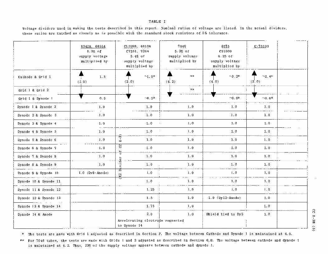
I
I
I
I
I
TABLE I Voltage dividers used in making the tests described in this report. Nominal ratios of voltage are listed. In the actual dividers, these ratios are matched as closely as is possible with the standard stock resistors of 5% tolerance.
6342A, 6655A CL1090, 6810A 7046 8575 C-70133 8.3% Of C7251, 7264 5.3% of C31000
supply voltage 5.4% Of supply voltage 6.1% Of multiplied by supply voltage multiplied by supply voltage
multiplied by multiplied by
Cathode & Grid 1 t 1. 5 t "'1.5* t ** t rv3. 2* t "'2. 4* ( 2. 0) (2. 0) ( 4. 2) ( 4. 0) (3. 0)
Grid 1 & Grid 2 ** ·- .. ·-Grid 1 & 1 ~ Dynode 0. 5 ~' rvo. 5* rvo. 8* rvo. 6*
Dyndde 1 & Dynode 2 I 1. 0 1. 0 1. 0 1. 0 1. 0
Dynode 2 & Dynode 3 1. 0 1. 0 1. 0 1. 0 1. 0
Dynode 3 & Dynode 4 1. 0 1. 0 1. 0 1. 0 1. 0
Dynode 4 & Dynode 5 1. 0 1. 0 1. 0 1. 0 1. 0 ~
M
Dynode 5 & Dynode 6 1. 0 I 1. 0 l. 0 1. 0 1. 0 00
I u Dynode 6 & Dynode 7 1. 0 u 1. 0 1. 0 1. 0 1. 0
"""" 0 Dynode 7 & Dynode 8 1. 0
~ 1. 0 1. 0 1. 0 1. 0
'"Cl Dynode 8 & Dynode 9 1. 0 ..... 1. 0 1. 0 1. 0 1. 0 >
.~
0 Dynode 9 & Dynode 10 1. 0 (Dy9-Anode)
;j 1. 0 1. 0 1. 0 1. 0
~
Dynode 10 & Dynode 11 1. 0 1. 0 1. 0 1. 0
Dynode 11 & Dynode 12 1. 25 1. 0 1. 0 1. 0
Dynode 12 & Dynode 13 1. 5 1. 0 1. 0 (Dy12-Anode) 1. 0
Dynode 13 & Dynode 14 1. 75 1. 0 1. 0
Dynode 14 & Anode 2.0 1. 0 Shield tied to Dy5 1. 0
Accelerating electro je connected
I to Dynode 14
* Tbe tests are made with Grid 1 adjusted as described in Section F. Tbe voltage between Cathode and Dynode 1 is maintained at 4. 0.
** For 7046 tubes, the tests are made with Grids 1 and 2 adjusted as described in Section G,H. The voltage between cathode and dynode 1 is maintained at 4. 2. Thus, 23% of the supply voltage appears between cathode and dynode 1.
I
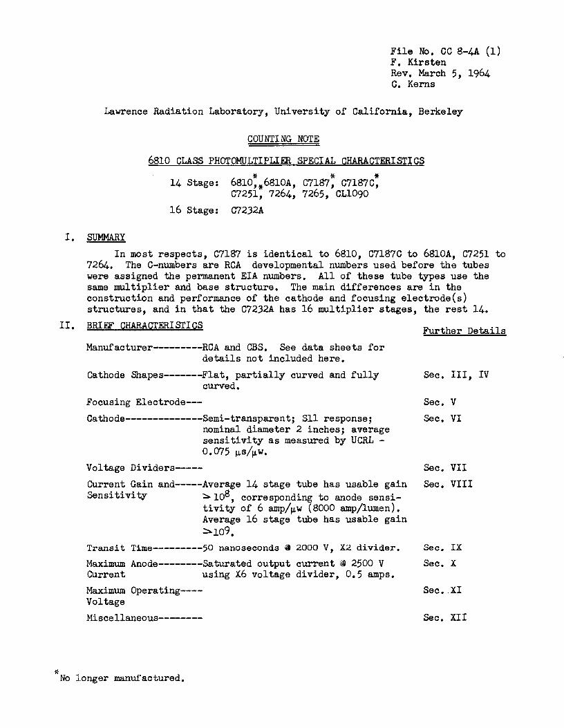
*
I.
II.
File No. CC 8-4A (1) F. Kirsten Rev. March 5, 1964 c. Kerns
Lawrence Radiation Laboratory, University of California, Berkeley
COUNTING NOTE
6810 CLASS PHOTOMULTIPLIER SPECIAL CHARACTERISTICS
14 Stage:
16 Stage:
SUMMARY
* 6810,*6810A, C7251, 7264, C7232A
* * C7187, C7187C, 7265, cL1090
In most respects, C7187 is identical to 6810, C7187C to 6810A, C7251 to 7264. The C-numbers are RCA developmental numbers used before the tubes were assigned the permanent EIA numbers. All of these tube types use the same multiplier and base structure. The main differences are in the construction and performance of the cathode and focusing electrode(s) structures, and in that the C7232A has 16 multiplier stages, the rest 14. BRIEF CHARACTERISTICS
Manu.f acturer---------RCA and CBS. See data sheets for details not included here.
Further Details
Cathode Shapes-------Flat, partially curved and fully Sec. III, IV curved.
Focusing Electrode--- Sec. V Cathode--------------Semi-transparent; Sll response; Sec. VI
nominal diameter 2 inches; average sensitivity as measured by UCRL -0.075 µs/µw.
Voltage Dividers----- Sec. VII Current Gain and-----Average 14 stage tube has usable gain Sec. VIII Sensitivity :::=i..108, corresponding to anode sensi-
tivity of 6 amp/µw {8000 amp/lumen). Average 16 stage tube has usable gain ~w9.
Transit Time---------50 nanoseconds @ 2000 v, X2 divider. Sec. IX
Maximum Anode--------Saturated output current ® 2500 V Sec. X Current using X6 voltage divider, 0.5 amps. Maximum Operating---- Sec •. XI Voltage Miscellaneous-------- Sec. XII
No longer manufactured.
cc 8-4A (2)
III. CATHODE SHAPES The various curvatures used in the cathodes of these tubes represent
efforts to minimize cathode transit-time difference, see Section IV.
INCIDENT LIGHT
Dashed line shows approx-imate limits of semi-transparent cathode area.
FLAT Used
Focusing Electrode
Square hole. --...,..__ Dynode 1
CATHODE-Shape B on: C7187
6810-before 1/57 C7232
0 "Molded 11 partially curved cathode-Shape D Used on: C7187C, 6810A,
C7232A after"" 6/51, 7265
'~round" partially curved cathode-Shape C
Used on: 6810 after 1/57 C7232A before ~ 6/57
Fully curved cathode-Shape G Used on: C7251
7264
Fig. 1 - Cross-sectional views showing the various cathode shapes.
IV. CATHODE TRANSIT-TIME DIFFERENCE In Fig. 2, curves of cathode transit-time difference (CTTD) are
shown for typical samples of each of the cahode shapes illustrated in Fig. 1. These curves of CTTD are typical. Variations may be expected among tubes of the same type, particularly among tubes of the C7251, fully curved cathode type. Fig. 2c is a typical curve for the C7251 type. Fig. 2d shows the extremes in CTTD characteristics that have been observed in C7251 tubes. The curves were all measured with cathode-dynode 1 voltages of 250-300 volts. Estimates of the characteristic for other voltages can be made using the relation that the magnitude of CTTD varies inversely as the square root of the voltage.
In general, CTTD curves recorded for tube diameters perpendicular to the long dimension of the dynodes are different from curves for parallel diameters. The CTTD curves for most of these tubes have a hook near the base-pin 4 edge of the cathode; the photoelectron collection efficiency is usually relatively poor in this same region. The measured CTTD includes the effect of differences in transit-time from dynode 1 to dynode 2. In general, photoelectrons from different parts of the cathode are focused onto different parts of dynode 1.
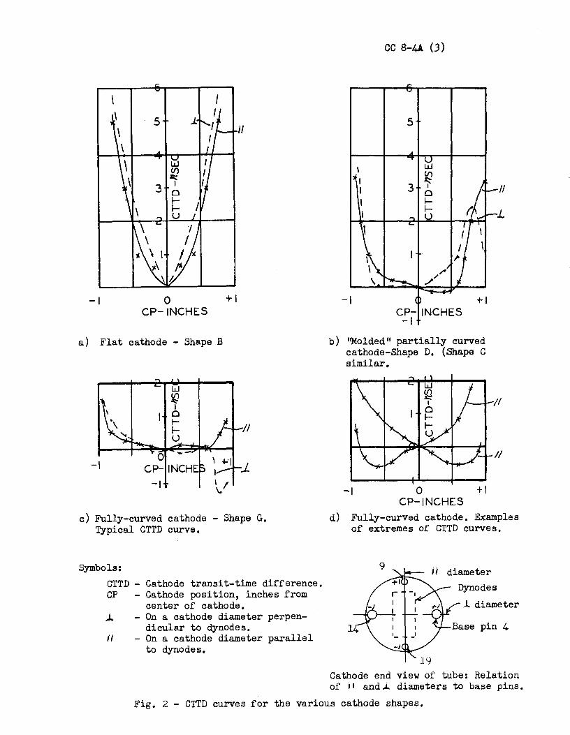
-I 0 CP-INCHES
JI
+I
a) Flat cathode - Shape B
---I \ +·1
I J. -1 '1 \.
c) Fully-curved cathode - Shape G. Typical CTTD curve.
Symbols: CTTD - Cathode transit-time difference. GP Cathode position, inches from
center of cathode. ).. - On a cathode diameter perpen-
dicular to dynodes. II - On a cathode diameter parallel
to dynodes.
-I
cc 8-4A (3)
5
w iQ 3 I 0 I-I-u
CP- INCHES -I
+I
b) "Molded 11 partially curved cathode-Shape D. (Shape C similar.
-I 0 +I CP-INCHES
II
II
d) Fully-curved cathode. Examples of extremes of CTTD curves.
diameter
l. diameter
1
Cathode end view of tube: Relation of i 1 and ...i.. diameters to base pins.
Fig. 2 - CTTD curves for the various cathode shapes.
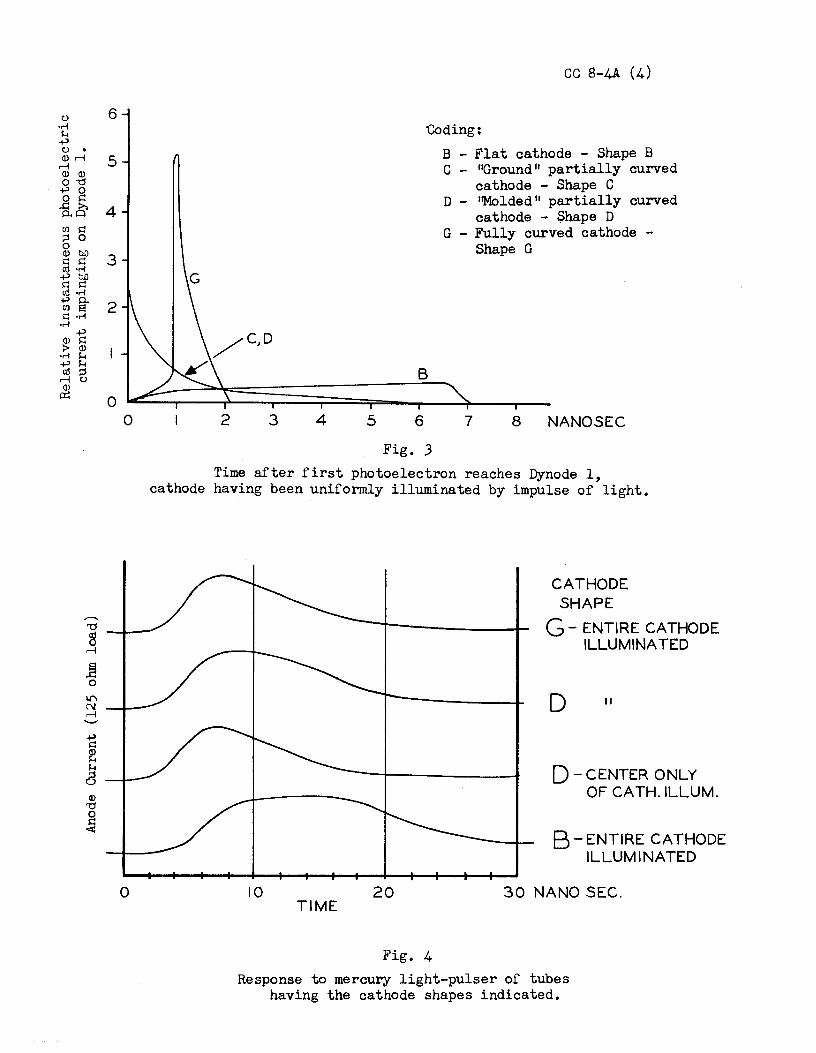
6
5
0 0
0
2 3 4 5
cc 8-4A (4)
'Coding:
B
6
Fig. 3
B - Flat cathode - Shape B C - "Ground" partially curved
cathode - Shape C D - ''Molded" partially curved
cathode - Shape D G - Fully curved cathode -
Shape G
7 8 NANOSEC
Time after first photoelectron reaches Dynode 1, cathode having been uniformly illuminated by impulse of light.
10 20 TIME
Fig. 4
CATHODE SHAPE
G - ENTIRE CATHODE ILLUMINATED
D II
D-cENTER ONLY OF CATH. ILLUM.
8 - ENTIRE CA THODE ILLUMINATED
30 NANO SEC.
Response to mercury light-pulser of tubes having the cathode shapes indicated.
cc 8-4A (5)
IV. CATHODE TRANSIT TIME DIFFERENCE (Continued) The curves in Fig. 3 show the response of the cathode-dynode 1 systems
of the 6810-class phototubes to an impulse (delta function) of light. These curves are derived from the CTTD curves of Fig. 2 using the assumptions that the cathode sensitivities and photoelectron collection efficiencies are uniform over the cathodes. If the input pulses were reduced in amplitude to the point where single photoelectrons were emitted from the cathode, the curves of Fig. 3 indicate the "time jitter" that may be expected in the delay between the light pulse and the anode output pulse.
The shapes of the anode pulses are modified from those of Fig. J by the multiplier transit-time spread. Fig. 4 shows anode pulses from tubes having these cathode shapes and illuminated by light pulses from a mercury-capsule light pulser. The light pulses rise and fall to 20% amplitude in about 1.5 nanosec, followed by a gradual decay, and thus roughly approximate an impulse compared to the response time of the tubes. Recent work with the mercury capsule light pulser has shown that light flashes as narrow as 300 picosec. can be realized by using low voltage on the mercury capsule.1
V. FOCUSING ELECTRODE The focusing electrode (Gl) and cathode (including the aluminized coat-
ing) form an electrostatic lens whose purpose is to focus photoelectrons onto dynode 1. The cross-sectional drawings of Fig. 1 show the physical relation of these parts. The potential of the focusing electrode affects not only the focusing of photoelectrons from the cathode onto dynode 1, but also the focusing of secondary electrons from dynode 1 onto dynode 2. The optimum operating voltage for the focusing electrode therefore depends upon both the voltage between cathode and dynode 1 (VK-Dl) and between dynode 1 and dynode 2 (VDl-D2). All figures quoted herein are based upon a voltage distribution of VK-Dl = 2 x VD1-D2' see Section VII.
The variation of anode sensitivity with the ratio of VK-FEIVK-Dl is shown in Fig. 4A, for two typical tubes. These curves are for the entire cathode illuminated. The value of this ratio giving the maximum anode sensitivity is called the optimum ratio, and varies from tube to tube. The statistical dis-tribution of the optimum ratios for a sample of 200 tubes is shown in Fig. 4B. The optimums range from 0.7 to 0.9.2 Most tubes give> 80% of the maximum anode sensitivity when operated at VK-F.EIVK-Dl of 0.8, but to obtain best per-formance from the tubes it is necessary to adjust the voltage dividers indi-dividually. Values of optimum ratio are marked on the tube base3 or are avail-able from the Physics Technical Support Group.
Type C7251 has an additional electrode, the "focus ring", mounted above the focus electrode, Fig. 1. In all but some of the earliest serial numbered tubes (made before 12/57) received to date, the focus ring is internally tied to the cathode.
Magnetic fields as low as one gauss may affect the optimum operating voltage for the focusing electrode; therefore all such determinations should be carried out after degaussing and with a magnetic shield in place.
1. M. Birk, 'II. A. Kerns, & R. F. Tusting, "Evaluation of' the C-70045H High Speed Photomultiplier", UCRL-11147 (Feb. 19, 1964)
2. Note disagreement with RCA data sheets. 3. Refer to CC 8-JA.

>-I-> I-C/) z w CJ)
w 0
~ <(
w > I-<( _J w ex:
CJ) w
cc 8-4A (6)
0.2 ...... --...... ~
0 ... ~-------"'-----....__ ___ ....__ __ ___. 0 0.2 0.4 0.6 0.8 1.0 tcATHODE RATIO- VK-FE tDYNODE I POTENTIAL
POTENTIAL VK-DI
Fig. 4A The variation of anode sensitivity with
focus-electrode (Gl) voltage with entire cathode illuminated.
70
60
50
cf) 40 ~ 1--1.J... 30 0 0:: ~ 20 L ~ z
10
0.70 0.80
VK-FE/VK-Dl
Fig. 4B
0.90
Distribution of optimum ratios of VK-FE/VK-Dl for 200 6810A tubes (1962-63)
CJ) w co :J I-
40
30
~ 20 er w co ~ :J z
10
0
..
...
-
..
A .. 10
cc 8-4A (7)
- 40 ... -
... 30 i-- -
... --- 20 - --- --
- .. -10 -- -- -- -r- 1-n,
30 o/o l5 20 25 A n- -.. 0
10 25% 15 20 6810A (19~ Samples) 7264 (190 Samples)
Fig. 5 - Cathode ~uantum Efficiency
VI. CATHODE SENSITIVITIES Fig. 5 shows the distribution of cathode quantum efficiencies measured
by Physics Technical Support Group on tubes received at UCRL in the year ending 12/63. The quantum efficiency is measured with radiation centered about 4200 Angstroms. It is the ratio of the number of photoelectrons emitted to the number of photons incident on the cathode. Cathode sensitivity and quantum efficiency are related by: Cathode sensitivity (µA/µWatt) x photon energy (electron volts) x 100 = quantum efficiency (per cent). Photons of 4200 Angstrom wavelength have an energy of 2.95 e.v.
VII. VOLTAGE DIVIDERS Voltage ratios and typical resistor values for three voltage dividers
are given in Table I. Of the tQree dividers, Xl gives the highest current gain for a given tube voltage, !6 the lowest. Divider X6 gives the highest saturated output current, Xl the lowest. (See Section VIII, X.)
Aside from the cathode-dynode 1 voltage: in divider Xl, all interdynode voltages are equal; in X2, higher voltages are applied to the last few stages, with the highest being twice (X2) the dynode 1 - dynode 2 voltage; in X6, the highest interdynode voltage is six times (X6) the dynode 1 - dynode 2 voltage.
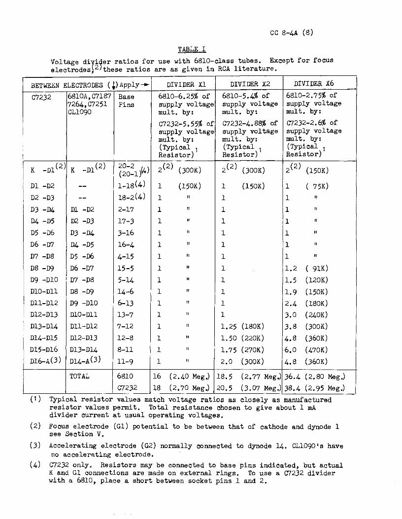
cc 8-4A (8)
TABLE I Voltage diyicter ratios for use with 6810-class tubes. Except for focus electrodes~2Jthese ratios are as given in RCA literature.
BETWEEN ELECTRODES ( t) Apply_... DIVIDER Xl DIVIDER X2 DIVIDER X6
C72.32 6810A, C7187 Base 6810-6.25% of 6810-5.4% of 6810-2.75% of 7264,C7251 Pins supply voltage supply voltage supply voltage CL1090 mult. by: mult. by: mult. by:
C72.32-5.55% of C72.32-4.88% of C72.32-2.6% of supply voltage supply voltage supply voltage mult. by: mult. by: mult. by: (Typical 1 (Typical 1 (Typical 1 Resistor) Resistor) Resistor)
K -Dl( 2) K -Dl( 2) 20-2 (4) (20-1)
2(2) (JOOK) 2(2) (.300K) 2(2) (150K)
Dl -D2 -- 1-18(4) 1 (150K) 1 (150K) 1 ( 75K) D2 -D.3 -- 18-2(4) 1 II 1 1 II
D.3 -D4 Dl -D2 2-17 1 " 1 1 " D4 -D5 D2 -D.3 17-.3 1 If 1 1 II
D5 -D6 D.3 -D4 .3-16 1 II 1 1 II
D6 -D7 D4 -D5 16-4 1 II 1 1 " D? -D8 D5 -D6 4-15 1 II 1 1 II
D8 -D9 D6 -D7 15-5 1 II 1 1.2 ( 91K) D9 -DlO D7 -D8 5-14 1 " 1 1.5 (120K) DlO-Dll D8 -D9 14-6 1 II 1 1.9 (150K) Dll-Dl2 D9 -DlO 6-1.3 1 II 1 2.4 (180K) Dl2-Dl.3 DlO-Dll lJ-7 1 II 1 .3. 0 (240K) Dl.3-Dl4 Dll-Dl2 7-12 1 II 1.25 (180K) .3. 8 (.300K) Dl4-Dl5 Dl2-Dl.3 12-8 1 II 1.50 (220K) 4.8 (.360K) Dl5-Dl6 Dl.3-Dl4 8-11 1 II 1.75 (270K) 6.0 (470K) Dl6-A(.3) Dl4-A(.3) 11-9 1 II 2.0 (.300K) 4.8 (J60K)
TOTAL 6810 16 (2.40 Meg.) 18.5 (2.77 Meg.) .36.4 (2.80 Meg.) C72.32 18 (2.70 Meg.) 20.5 (.3. 07 Meg.) .38. 4 ( 2 • 9 5 Meg .)
(1) Typical resistor values match voltage ratios as closely as manufactured resistor values permit. Total resistance chosen to give about 1 mA divider current at usual operating voltages.
(2) Focus electrode (Gl) potential to be between that of cathode and dynode 1 see Section V.
(.3) Accelerating electrode (G2) normally connected to dynode 14. CL1090's have no accelerating electrode.
(4) C72.32 only. Resistors may be connected to base pins indicated, but actual K and Gl connections are made on external rings. To use a C72.32 divider with a 6810, place a short between socket pins 1 and 2.

z 10 7 <{ 0 1-z w a:: a:: '.:)
cc 8-4A (9)
u 181- POINT AT WHICH REGENERATION OCCURRED
10
500 1000 1500 2000 2500 V AK -ANODE- CATHODE VOLTAGE_, VOL TS
Fig. 6 Anode current gain and sensitivity of a typical 14 stage 6810-class tube. This tube has a "standard sensi ti vi ty 11 of 1. 6 a/µ. W at 1860 vol ts and would the re-f ore have 111860 11 marked on the tag attached to it by Physics Technical Support Group, see CC 8-3)
(/) w
40
en 30 '.:)
I-LL 0 20 er: w ((}
~ 10 :::::> z
1600 1800 2000 2200 2400 ANODE- CATHODE VOLTAGE (X2 DIVIDER)
Fig. 7 Distribution of anode-cathode voltages required to obtain "standard sensitivity" of 1.6 a/µ.W in 228 6810's received in 1962 - 1963.
3000
cc 8-4A (10)
VIII. ANODE CURRENT GAIN AND SENSITIVITY In Fig. 6 are curves of anode sensitivity and current gain for a typical
14-stage tube of the 6810 class. For a given divider, the maximum operating voltage of such a tube is usually determined by light feedback; thus, as shown, the maximum gains obtained with the three dividers are about the same. This maximum gain varies less than an order of magnitude from tube to tube.
The voltage at which the sensitivity of 1.6 amps/µwatt ~ 4200 ~ (2000 amps/lumen or gain of l'V 3 x 10⁷) is obtained with an X2 divider is marked on the tube base by Physics Technical Support Group (see CC 8-3 for code). The statistical distribution of such voltages on recent 6810A tubes is shown in Fig. 7. Near this voltage, the gain and anode sensitivity change about an order of magnitude per JOO volts.
When space-charge saturation effects, see Section IX, are absent, the dynode-14 gain (dynode 16 in C7232) is the anode gain times (S-1)/S, where S is the secondary emission ratio of dynode-14. ~depends on the voltage and is typically of the order of 3.5 at a sensitivity of 1.6 a/µW.
For several reasons, the "local" anode sensitivity measured by illuminating small parts of the cathode is a function of the area illuminated. Typically, these, local variations amount to ± 20% of the mean sensitivity, except that the cathode area opposite base pin 4 usually has much lower sensitivity than the mean. This latter effect is apparently associated with the portion of dynode-1 at which photoelectrons from this area strike.
Fig. 8 gives gain and sensitivity curves for a C7232A. The maximum usable gains have been found to range from 4 x 10⁹ to 5 x 10¹⁰ in a sample of 5 tubes.
10 11
1o'O
109
z <( 108 C>
I-JO 7 z
w 0:: 0::
106 ::::> u
105
SPACE-CHARGE SATURATES WITH SINGLE PHOTOELECTRON:S -
RANGE OF MAX.
1000
OPERATING VOLTAGES FOUND IN SAMPLE OF 5
C7232
1500 2000 2500 3000 VOLTS-ANODE-CATHODE
Fig. 8 - Gain-voltage curves of C7232.
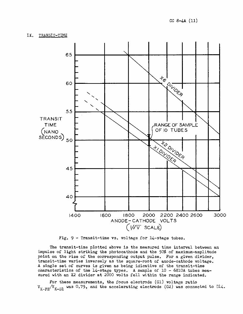
IX. TRANSIT-TIME
TRANSIT TIME
65
60
cc 8-4A (11)
+6' to-~~~~-+-~~~-+~~~ ...... ~~ <'.)/i.-'.
0 ~~
' '
RANGE OF SAMPLE OF 10 TUBES (NANO
SECOND s) 5 O t------t-----+--..,,,,_--11~----+---+---t---1
1400 1600 1800 2000 2 200 2400 2600 3000 ANODE-CATHODE VOLTS
(VIV SCALE)
Fig. 9 - Transit-time vs. voltage for 14-stage tubes.
The transit-time plotted above is the measured time interval between an impulse of light striking the photocathode and the 50% of maximum-amplitude point on the rise of the corresponding output pulse. For a given divider, transit-time varies inversely as the square-root of anode-cathode voltage. A single set of curves is given as being idicative of the transit-time characteristics of the 14-stage types. A sample of 10 - 6810A tubes mea-sured with an X2 divider at 2000 volts fell within the range indicated.
For these measurements, the focus electrode (Gl) voltage ratio VK-FE/vK-Dl was 0.75, and the accelerating electrode (G2) was connected to Dl4.
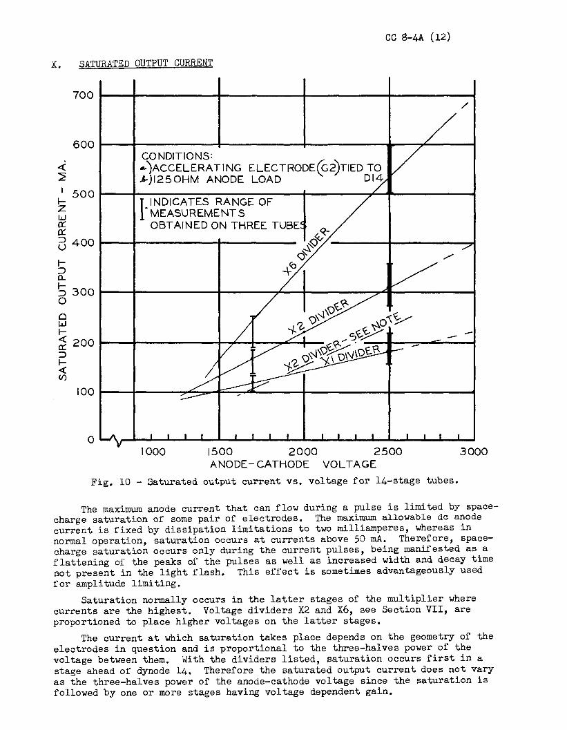
cc 8-4A (12)
X. SATURATED OUTPUT CURRENT
700
600
<( ~ I
I-500
z w 0::: 0::: ::> 400 u t-:::> a.. f- 300 :::> 0 0 w f-<( 200 0::: :::> f-<( Cf)
100
0
CONDITIONS: ... )ACCELERATING ELECTRODE(G2)TIED TO ..4-)1250HM ANODE LOAD Dl4
I_ INDICATES RANGE OF MEASUREMENTS OBTAINED ON THREE TUBE
1000 1500 2000 ANODE-CATHODE
2500 VOLTAGE
--
Fig. 10 - Saturated output current vs. voltage for 14-stage tubes.
/
-
3000
The maximum anode current that can flow during a pulse is limited by space-charge saturation of some pair of electrodes. The maximum allowable de anode current is fixed by dissipation limitations to two milliamperes, whereas in normal operation, saturation occurs at currents above 50 mA. Therefore, space-charge saturation occurs only during the current pulses, being manifested as a flattening of the peaks of the pulses as well as increased width and decay time not present in the light flash. This effect is sometimes advantageously used for amplitude limiting.
Saturation normally occurs in the latter stages of the multiplier where currents are the highest. Voltage dividers X2 and X6, see Section VII, are proportioned to place higher voltages on the latter stages.
The current at which saturation takes place depends on the geometry of the electrodes in question and is proportional to the three-halves power of the voltage between them. With the dividers listed, saturation occurs first in a stage ahead of dynode 14. Therefore the saturated output current does not vary as the three-halves power of the anode-cathode voltage since the saturation is followed by one or more stages having voltage dependent gain.
cc 8-4A (13)
One may choose to define saturation as occurring at the current for which there is an appreciable widening in the output pulse. This method is described in EE-795 and is there defined as the current at which there is a 25% increase in pulse width at the half-height.
Note: Some tubes have an altered Dl4-anode configuration which saturates at a lower value of current as indicated by the dashed curve for the X2 divider above. This new configuration has been built into some tubes made after April, 1958, bearing serial numbers starting with 4.8.XXXX. These tubes may be identified by a vacant hole in the side support insulator at the old anode position.
XI. MAXIMUM OPERATING VOLTAGE The maximum operating voltage is the maximum voltage that may be
applied to a tube without causing harmful effects either to the tube or to the operation of the following circuits. As the voltage is increased, the anode dark current (amplified cathode dark current) likewise increases; in tubes where regenerative effects are present, at some voltage the dark current will suddenly increase to the limit determined by the divider. If the divider allows the anode current to exceed one milliampere, excessive power dissipation within the tube may degrade certain of its properties. Even if the divider limits the current to a layer value, the interelectrode currents flowing in the divider cause a redistribution of voltages which usually lowers the tube gain and the saturated output current.
Experimental evidence indicates that, in most 6810 1 s light feedback * within the tube determines the maximum gain that may be attained. Refer to Fig. 6 where it is seen that the maximum gain available from the parti-cular tube shown is very nearly the same regardless of the divider used. Thus, low-gain tubes will, in general, have higher maximum operating voltages than high-gain tubes.
The use of reflecting materials (aluminum foil, etc) next to the glass envelope of the tube may enhance the light feedback, lowering the maximum attainable gain and tending to increase the noise. Electrostatic shielding should be constructed in a way that does not provide a path for light to be transmitted from the anode to the cathode.
The maximum operating voltage is measured for each tube and is marked on the round sticker on the tube base by Counting Maintenance, see CC 8-3.
* Approximately 50 nanoseconds (one transit-time) after a light pulse strikes the cathode, a pulse of electrons reaches the last few dynodes. Light is produced by these inter-dynode electrons. Some of the light leaks back to the cathode resulting in afterpulses at multiples of one transit-time after the original pulse. When the gain is increased to the point that the first such afterpulse is greater than the original pulse, a regenerative condition is reached.
cc 8-4A (14)
XII. MISCELLANEOUS 1. Magnetization
Certain parts of the tubes (e.g. the focus electrode and the sealing ring at the base end) may become permanently magnetized upon exposure to a strong enough magnetic field. Tubes known to have been exposed to a 100 gauss field in the Bevatron building have been found to give 1/10 their normal gain at a given voltage. The minimum field required to cause magnetization has not been measured. Normal operation is recovered upon being demagnetized; no permanent after effects have been noted.
It is recommended that tubes be mounted in their magnetic shields before being carried into locations where magnetic fields greater than the order of ten gauss are to be encountered.
2. Sources of Excess Noise Within the Tube (cf. Section XI - light feedback).
CK:mt
A common source of tube failure has been found to be the "glowing filament"· It consists of a small whisker or filament of semi-conducting material which may become lodged between two electrodes, thereby shorting the associated voltage divider resistors. The whiskers usually glow visibly at currents of the magnitude flowing in voltage dividers. The symptoms of a tube with a glowing filament, therefore, are: reduced gain, owing to the shorted electrodes; a higher cathode dark current, owing to the light produced by the fila-ment.
Methods of evaporating the filament and returning the tube to its normal condition are covered in Engineering Note EE-521, or refer to Physics Instrumentation Research Group, Bldg. 80, Room 13.
Discharges may occur between various electrodes in certain tubes because of sharp points, rough surfaces, etc. When present, such discharges often increase the dark current (noise) by several times. In cases where these sources can be located (e.g. visually), they may often be burned off by establishing the glow with a current of a few µA, then discharging a suitable pulse of electrical energy ,,.., 5 millijoules through the discharge.
The excess noise which is produced by effects other than cathode thermionic emission often is not materially reduced by lowering the temperature of the tube.
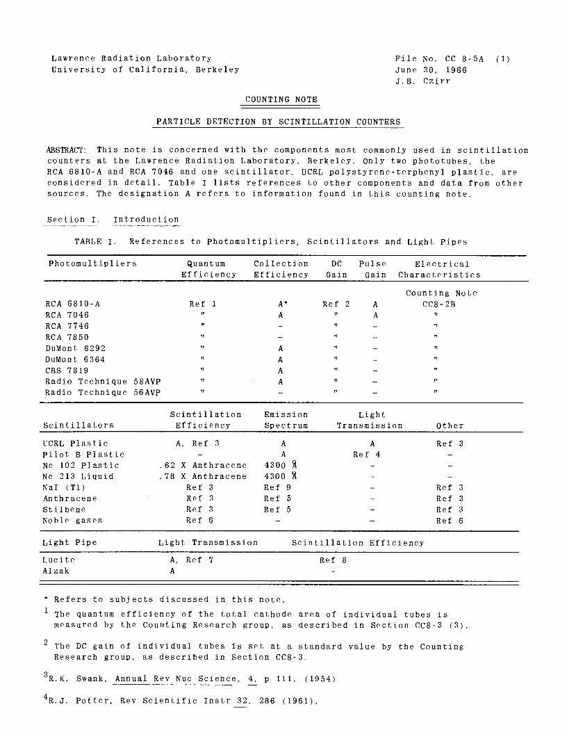
Lawrence Radiation Laboratory University of California, Berkeley
COUNTING NOTE
File No. CC 8-5A (1) June 30, 1966 J.B. Czirr
PARTICLE DETECTION BY SCINTILLATION COUNTERS
ABSTRACT: This note is concerned with the components most commonly used in scintillation counters at the Lawrence Radiation Laboratory, Berkeley. Only two phototubes, the RCA 6810-A and RCA 7046 and one scintillator, UCRL polystyrene-terphenyl plastic, are considered in detail. Table I lists references to other components and data from other sources. The designation A refers to information found in this counting note.
Section I. Introduction
TABLE I. References to Photomultipliers, Scintillators and Light Pipes
Photomultipliers Quantum Efficiency
RCA 6810-A RCA 7046 RCA 7746 RCA 7850 DuMont 6292 DuMont 6364 CBS 7819 Radio Technique Radio Technique
Scintillators
UCRL Plastic Pilot B Plastic Ne 102 Plastic Ne 213 Liquid Na! (Tl) Anthracene Stilbene Noble gases
Ref 1 " " " " " "
58AVP " 56AVP "
Scintillation Efficiency
A, Ref 3
.62 x Anthracene
.78 x Anthracene Ref 3 Ref 3 Ref 3 Ref 6
Collection Efficiency
A* A
A A A A
Emission Spectrum
A A
4300 ~ 4300 ~ Ref 9 Ref 5 Ref 5
Pulse Electrical DC Gain Gain Characteristics
Ref 2 A " A " " " " " " "
Light Transmission
A Ref 4
Counting Note CC8-2B
" " " " " " " "
Other
Ref 3
Ref 3 Ref 3 Ref 3 Ref 6
Light Pipe Light Transmission Scintillation Efficiency
Lucite Alzak
A, Ref 7 A
* Refers to subjects discussed in this note.
Ref 8
1 The quantum efficiency of the total cathode area of individual tubes is measured by the Counting Research group, as described in Section CC8-3 (3).
2 The DC gain of individual tubes is set at a standard value by the Counting Research group, as described in Section CC8-3.
3R.K. Swank, Annual Rev Nuc Science, 4, p 111. (1954)
4R.J. Potter, Rev Scientific Instr 32, 286 (1961).

CC8-5A (2)
The following general relation may be used to arrive at an estimate of the signal magnitude to be expected from a given evento It should be noted in applying this relation that there are,at present, 20% uncertainties in some of the measured quantities which p.lace a limit on the precision of the resulto It is for this reason that the approximations used below ar8 admissable.
Let
N (£0
,m) =fixd°i • df'.'. • d\ A(£,m,\) 0 B(\) • c(l,\) · D(7,\) • E(x) • F = average number of electrons at anode per incoming particle of energy
e and mass m. 0
Where A=
B = c =
D = E = F =
number of photons detectable by the phototube/MeV lost/unit wave-length (for scintillator in use). fraction of photons striking cathode (for scintillator and light pipe in use). -) quantum efficiency at position r and wavelength \ (for tube in use) or number of electrons leaving per photon striking cathode. collection efficiency at position --f and wavelength >.. from cathode to dynode 1 (for tube in use). collection efficiency from dynode 1 to anode as a function of dynode positions x (for tube in use). pulse gain of tube used = gain of the tube for those pulses which yield a detectable anode pulse.
Note~ D 0 E • F = G = de gain = anode current cathode current
or i = DE = probability of successf·cllly obtaining an anode pulse per
photoelectron. 1. Let A(e,m,:>..)-;:-A'(El'm) •A"(\). See Ref. 10 for evidence that the
emission spectrum is independent of the type of exciting particle. A'(e,m) =number of photons/MeV lost (at all wavelengths detected by the photomultiplier). l/A 1 (E,me) = 100 ± 20 ev/photon for all e in plastic scintillator. or A'(e,m) = (1±0.2)x104 photons/MeV. See Ref. 3 for anthracene, NaI, etc.eev/photon. See Ref. 6 for plastic scintillator to anthracene ratio. Form Im see Ref. 11~ or Section II.
~F. D. Brooksl' Prog i: Nuclear Phys, 5, p. 252 (1956). Methods of Experimental Phys, p. 127 (Academic Press), (1961).
7P. R. Bell and C.C. Harris, IRE NS-3 9 Transactions on Nuclear Science 4, p. 87 (1956).
8 R. Madey and L. Leipuner~ Nucleonics lit p. 51 (April 1956).
9 W. J. Van Sciverj Nucleonics lit~ p. 50 (April 1956). 10
11
W. L. Buck and R. Ko Swank, Nucleonics 11, p 48 (Nov. 1953), W.S. Koski and C. O. Thomas, Phys Rev 7.51~ p. 217. J. M. Fowler, C. Eo Roos~ Phys Rev~' p. 996 (1955), C. J. Taylor, W. K. Jentsch~e, M. E. Remley~ F. S. Eby, and P. G. Kruger Phys Rev 84 p. 1034 (1951), M. Gettner ana W, Selovej Rev. Scio Instr. ll, 450 (190IT~.

2.
J.
4.
5.
CC 8-5A (3)
A"(>..) = fraction of photons at >.. per unit wavelength. See Section III. (Also the net output curve of Ref. 12 can be divided by 1P21 phototube response to get scintillator output spectrum. This applies to Livermore scintillator only.) See Ref. 5 for other scintillators.
B(\k See Section IV and Ref o 7. For calculations of the fraction of light produced in a scintillator which strikes a photo-cathode see Ref. J4.
C(2n f'Rrdr, 4400 1) for R = R is given with each tube at Lawrence Radiaftion Laboratory. For otfi~ :>-., the information~ in the tuby., data sheet and Section V. Q. A. Kerns has measured C(21:-6 ~· rdr, 4400 A ) for a few tubes of several types for various R < R (unpublished). max
(R o D(2n--b rdr, 4400 A~ for most tube ~YPcflEift~~t~}ned in Ref. 13 in another form. What is really ghown is CDE (Du Mont 6292 ) as a function of subtended area and at 4400 A. See Section VI for DE curves for several tube types. The authors of Ref. 13 state that C is constant enough in radius that the average C given may be used for all radii. They used a small central cathode area of a Du Mont 6292 as the closest thing to 100% photoelectron collection efficiency available. However, for this tube, D is probably less than 95% from statistics alone and could be even less. D could vary somewhat with >.. -- how much is unknown.
E(x). See 4 above" E (x) for the Du Mont 6292 may again be considerably less than 100%. We therefore have an upper limit on the absolute value of D • E (type i) from UCRL-9980.
Note: Q. Kerns estimates that D • E is greater than 0.80 for the central region of the Du Mont 6292 used as a standard.
6. See Section VII for a technique used to experimentally determine the number of detected photoelectrons.
12L. lcgne-w, Transmission Properties of Lucite Samples in the Photo-Multiplier :tesponse Il.egion, Lawrence Radiation Laboratory Report, UCID 889.
l3Fc •. f. Tusting, '~. A. Kerns, H. K. Knudsen, Photomultiplier Single-Electron Jtatistics, Lai,:rence Radiation Laboratory Report, UCRL-9980.
14'1 .3 . . Pl' 0 R' d' d T V . N c· t II .. . rin1, '" e i, • imon i, an • erones1, uovo 1men o, _, .Series i, ]. 4, Supp., P 1043, (1955)

Jcctfon Il. Scintillator l'~i'f lciency vs. Particle tlia.ss CC 8-5A (4)
•• .. i:;; •• ,.
, .. oO
1...=;:=.::~:--...._-:,± •• :--'---:l, .. :;;--...1--:.-!a.oo'--7',o~o--"--7 ••• NOTO. 1.NUl'f'
•••
{a) Pulse heights from anthracene and stilbene as a t'unct.ion of proton energy.
10 ..
10
100 zoo ... 100 ••• ... (c) K-ray energy versus proton energy for equal pulse heights.
10.---.-...... --...... --..---.......... --...... --,........,--..,
.. = ;30 - .. .. -z z ~
. zo .. . .. 0: ..... ~-• 10
0 I 10 11 ZO U.. 10 31 40 41 10 X· NAY lNlNCIY
UV
{b) Pulse heights from anthracene and stilbene as a function of x-ray energy.
-!.•o ·;; J: . l
t 1-~ ·0
f -1 ~
-r-=--r--c-T---l~!. -~ • ,:o I '
~' 1.0 J.O [ n•91 i11 MeY
(d) Pulse heights versus proton energy for stilbene. Experimental data oi'
Chagnon normalized to the curve at J.J MeV.
l•'igure 1. Pulse Ileir;h t vorsus energy (From Fowler and Roos).

Section III. Scintillator Spectral Response
Joo--- ----1 ----- --- - -;r-i\ -- ---~--· ---r--- ·- ----i----~-
CC 8-5A (5)
NOTE: For ~>38ooR, the light is rapidly atten-uated by transmission through the scintillator. The dashed curve shows the effective cut off for transmitted light.
Figure 3. Pilot Scintillator B Characteristics. Pulse Height: 90% of stilbene. Decay time: 2 x lQ-9 sec. Color: Clear, exhibits a blue daylight fluor-escence. Light Transmission: At peak fluorescence wavelength, transmission through a 1 foot length is 90~. Specific Gravity: 1.02. Composition: 100% hydrocarbon. Atomic Ratio: c=l.10. Softening Temperature: 70-75°C. Refractive Index: 1.58. Solubility: Insoluble in water and lower alcohols, soluble in numerous aromatic solvents. Information from Scintillation Grade Fluors, Pilot Plastic Scintillators, Pilot Chemicals, Inc., 36 Pleasant Street, Watertown, Massachusetts.
Section IV. Light P_!i>es
1. The transmission of various light pipes was measured within a dark box using a UCRL Mercury pulser light source. The data obtained are shown.
15L. F. Wouters, the UCRL Plastic Fluor, University of California, Lawrence Radiation Laboratory Report UCRL-4516, September 16, 1955.
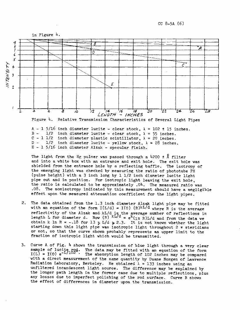
1 B 7 (,
5
~
"'--
CC 8-5A (6)
in Figure 4. -- -~
f'..._ -- B ~ -==-- "A
['--.._ 0 --- ,___
~ --r-----_
~ -~ c I--" -~
~~ t'----_£
? ID 12 14 16 18 '20 L£11c;rH - !N'<HeS
2t 2.4 .. 6
Figure 4. Relative Transmission Characteristics of Several Light Pipes
A 1 5/16 inch diameter lucite - clear stock, >. = 102 ± 15 inches. B 1/2 inch diameter lucite - clear stock, I. = 55 inches. c 1 1/2 inch diameter plastic scintillator, I. = 29 inches. D - 1/2 inch diameter lucite - yellow stock, I. = 28 inches. E - 1 5/16 inch diameter Alzak - specular finish.
The light from the Hg pulser was passed through a 4200 ± R filter and into a white box with an entrance and exit hole. The exit hole was shielded from the entrance hole by a reflecting baffle. The isotropy of the emerging light was checked by measuring the ratio of phototube PH (pulse height) with a 3 inch long by 1 1/2 inch diameter lucite light pipe out and in position. For isotropic light leaving the exit hole,
" .c.8
the ratio is calculated to be approximately .04. The measured ratio was .08. The nonisotropy indicated by this measurement should have a negligible effect upon the measured attenuation coefficient for the light pipes.
2. The data obtained from the 1.3 inch diameter Alzak light pipe may be fitted with an equation of the form I(L/d) = I(O) (R)kL/d where R is the average reflectivity of the Alzak and·.kL/d i~ the average number of reflections in length L for diameter d. Now (R) kL/d = ek(ln R)L/d and from the data we obtain k ln R = -.18 for 13 } L/d 7 2.3. It is not known whether the light starting down this light pipe was isotropic light throughout 2 w steridians or not, so that the curve shown probably represents an upper limit to the fraction of isotropic light which would be transmitted.
3. Curve A of Fig. 4 shows the transmission of blue light through a very clear sample of lucit~ ro~. The data may be fitted with an equation of the form I(L) = I(O) e-L/l02 • The absorption length of 102 inches may be compared with a direct measurement of the same quantity by Duane Norgen of Lawrence Radiation Laboratory, Berkeley. He obtained I. = 133 inches using an unfiltered incandescent light source. The difference may be explained by the longer path length in the former case due to multiple reflections, plus any losses due to imperfect polishing of the rod surface. Curve B shows the effect of differences in diameter upon the transmission.
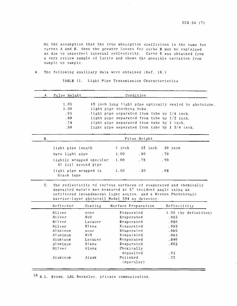
CC8- 5A ( 7)
On the assumption that the true absorption coefficient is the same for curves A and B, then the greater losses for curbe B may be explained as due to imperfect internal reflectivity. Curve D was obtained from a very yellow sample of lucite and shows the possible variation from sample to sample.
4. The following auxiliary data were obtained (Ref. 16.)
TABLE II. Light Pipe Transmission Characteristics
A. Pulse Height Condition
1. 05 15 inch long light pipe optically sealed to phototube. 1. 00 light pipe touching tube. .95 light pipe separated from tube by 1/4 inch. . 89 light pipe separated from tube by 1/2 inch. . 74 light pipe separated from tube by 1 inch. . 50 light pipe separated from tube by 1 3/ 4 inch.
B. Pulse Height
light pipe length bare light pipe tightly wrapped specular
Al foil around pipe light pipe wrapped in
black tape
1 inch 1. 00
1. 00
1. 00
15 inch 30 inch . 90 . 70
. 75 . 70
. 20 . 08
C. The reflectivity of various surfaces of evaporated and chemically deposited metals was measured at 5° incident angle using an unfiltered incandescent light source, and a Weston Phototronic barrier-layer photocell Model 594 as det~ctor.
Reflector Coating 'Surface Preparation Reflectivity
Silver none Evaporated 1. 00 (by definition) Silver SiO Evaporated .985 Silver Lacquer Evaporated .980 Silver Glass Evaporated . 99 3 Aluminum none Evaporated .895 Aluminum SiO Evaporated . 895 Aluminum Lacquer Evaporated . 840 Aluminum Glass Evaporated .862 Silver Glass Chemically
deposited .92 Aluminum Alzak Polished . 73
(specular)
l6 R. L. Brown, LRL Berkeley, private communication.

CC 8-5A (8)
/00
80 6tJ 40 -
20 0
3000 4000 5000 WAV£ l£NtiTH
7000
Figure 5. Spectral Sensitivity of Photronic Cells
Sectiop~~· Spectral Sensitivity Characteristics
Figures 6 and 7 give the spectral sensitivity characteristics for the types 6810-A and 7046 phototubes respectively. For other types see Counting Note CC8-2.
').., }UC f-. ~--;; t Bo ·--v) <::
- RAJ./(,£ Of MAX'- VAWE
c}) 60
~ I f"• 4-C· .--1·---+---I ~ I ~- 201/ ---+ ---+ l __ j_.~: __ _j __ ___.___,
~OU S6r10 7~0 qfJtj() 11,ox WA1 1[ t.ENOH - AtMSTROMS
Figure 6. Spectral Sensitivity Characteristic Type 6810-A which has S-11 Response. Curve is shown for Equal Values of Radiant Power at All Wavelengths.
~ \::: 4CJ1--~++-~---<f---<•--+-~--t--1
'S ~~bl----'1-+-~--'~~-+--~--f--j
0/000 ,3060 SOfXJ 'lOOO Cl30 WAV£L£Nf/rH -/-llKiSTR.OMS
Figure 7. Tentative Spectral Sensitivity Characteristic of Type 7046. Curve is shown for Equal Values of Radiant Flux at All Wavelengths.
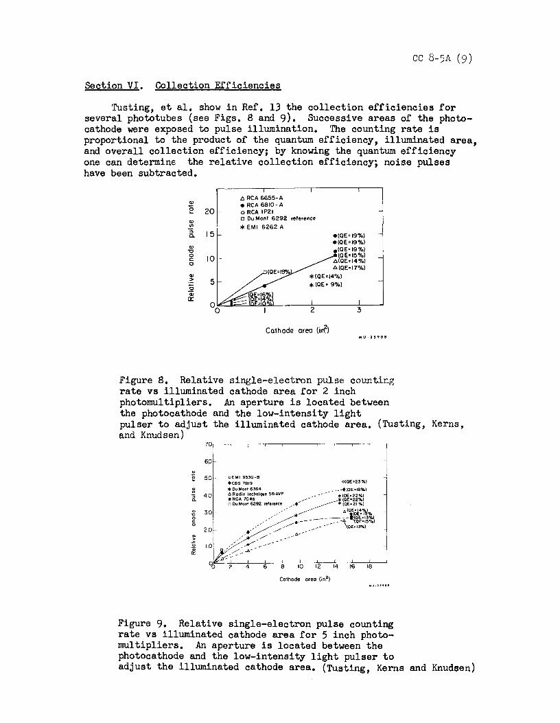
CC 8-5A (9)
Section VI. Collection Efficiencies
Tusting, et al. show in Ref. 13 the collection efficiencies for several phototubes (see Figs. 8 and 9). Successive areas of the photo-cathode were exposed to pulse illumination. The counting rate is proportional to the product of the quantum efficiency, illuminated area, and overall collection efficiency; by knowing the quantum efficiency one can determine the relative collection efficiency; noise pulses have been subtracted.
ti. RCA 6655-A <ll eRCA6810-A "§ 20 o RCA IP21
<ll o Du Mont 6292 reference
I/) * EMI 6262 A :; 15 e(QE= 19%) c. e(QE=19%)
<ll elQE=19%) "O 0 10 (QE=15%) c: ti.(QE=l4%) 0
fl.(QE=17%) <ll *lQE=14%) > 5 0 *(QE• 9%) Qi a::
2 3
Cathode area (irfl MU. 2 S 9 08
Figure 8. Relative single-electron pulse counting rate vs illuminated cathode area for 2 inch photomultipliers. An aperture is located between the photocathode and the low-intensity light pulser to adjust the illuminated cathode area. (Tusting, Kerns, and Knudsen)
60
"' ~ 5.0
:i: -,; 4.0 c.
oEMI 9530-8 +ces 1e19 O(QE•23%)
*Ou Mont 6364 ----+tOE=IB%) 6 Radio technique 5BAVP ------ •tQE=22•4)
o Ou Mont 6292 reference /~+- (QE•21 %)
~ 3.0
e RCA 7046 ~-- (0E•22%)
__ ,,, ,,1a~<ik'!."n/,.. ,» ,.--->!< - - - _1!,'aE•13%) 0
<: 0
2.0 .. ...- " ,.......-•- - - _ ... - - -, 9i:OE" 15°!.)
+' ' /- ---- OE•l3%) ~ ,. / 6---
~ 1.0 /_:>:-:-----ct: ~----
q) 2 4 6 8 10 12 >4 16 18
Cathode area (i n2)
Figure 9. Relative single-electron pulse counting rate vs illuminated cathode area for 5 inch photo-mul tipliers. An aperture is located between the photocathode and the low-intensity light pulser to adjust the illuminated cathode area. (Tusting, Kerns and Knudsen)
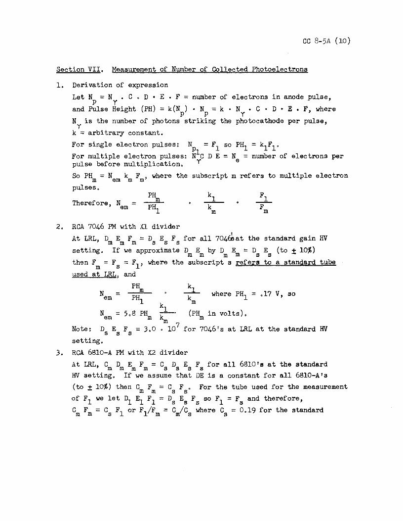
CC 8-5A (10)
Section VII. Measurement of Number of Collected Photoelectrons
1. Derivation of expression Let N = N • C • D • E • F = number of electrons in anode pulse,
p y and Pulse Height (PH) = k(N ) • N = k • N • C • D • E • F, where p p y N is the number of photons striking the photocathode per pulse, y k = arbitrary constant. For single electron pulses: For multiple electron pulses: pulse before multiplication. So PH = N k F Y where the m em m m pulses.
Therefore, N = em
N = F1 so PH1 = k1F1 • pl N C D E = N = number of electrons per y e
subscript m refers to multiple electron
2. RCA 7046 PM with Xl divider
3.
' At LRLj D E F = D E F for all 704Esat the standard gain HV m m m s s s setting. If we approximate D E by D E = D E (to ± 10%) m m m m s s then F = F = F19 where the subscript s refers to a standard tube m s used at LRLj and
N = em PH m
N = 5.8 PH em m Note: D E F = 3.0 s s s setting. RCA 6810-A PM with X2
~ k where PH1 = .17 V, so m
(PH in volts). m
for 7046's at LRL at the standard HV
divider At LRL, C D E F = C D E F for all 6810 1s at the standard m m m m s s s s HV setting. If we assume that DE is a constant for all 6810-A's (to + 10%) then C F = C F • For the tube used for the measurement - m m s s of F1 we let D1 E1 F1 = Ds Es Fs so F1 = Fs and therefore, C F = C F1 or F1/F = C /C where C = 0.19 for the standard mm s m ms s
4.
tubep so
N em PH m
Now PH1 = 0.076 V, so
Measurement of Pulse Height
(PH in V m C in decimals) m
(PH).
CC 8-5A (11)
Using the ~roper phototube divider, the anode signal (not back terminated) was fed through a short length df RG 63/U 125 O cable into a Tektronix B 170-A, 170 Q scope attenuator :in parallel with 470 Q to ground. In both cases the phototube HV was ~et such that the quantity D • E • F (de gain) was equal to 3.0 x 10⁷. The Tektronix 517 A scope w~s calibrated on the 0.5 V (10 Q) scale at 1/5 full scale using the 170 Q signal cable directly from calibration output to signal input. The sensitivity with no attenuation was then 0.10 V/cm. Any further attenuation should be obtained from the 170 Q attenuator box. The scope trigger was obtained from the Hg pulser light source used to obtain the single photoelectrons. The light repetition rate was 60 per second and the intensity was attenuated until only approximately 6 pulses per second were detected. In this condition only 1/20 of the pulses were due to 2 or more photoelectrons. The values given for PH1 in section 2 and 3 have been corrected for multiple electron pulses. The factor of 2 difference from 6810 A to 7046 PH1 is a reflection of the lower collection efficiency of the 7046. The assumption is made in this measuring technique that there is no contribution to many electron pulse heights from very small but numerous pulses which would have been invisible in the ab~ve method.
5. Measurement of k1/km.
A rough determination of k1/kro was made under the assumption that the charge contained in an anode pulse is proportional to the product of PH and full width at half maximum. The values for the RCA 6810 A are:
PH number of e kl/km
.076 v 1 1.00 2.82 v 37 1.46
and for the RCA 7046
PH number of e kl/km
.173 v 1 1.00 3.6 v 21 1.27

Radiation Laboratory, University of California, Berkeley
COUNTING NOTE
ELECTRICAL GATING OF MULTIPLIER PHOTOTUBF.s
I. Introduction:
File No. cc8-20 Page 1 December 29,· 1958 F. Kirsten
Several useful methods of gating multiplier phototubes are available. This note is primarily concerned with gating by means of controlling the voltages on the phototube electrodes. Several advantages of this method make it attractive for Ill8.Dy applications:
(1) A relatively high speed - most tubes may be turned on or off in a few nano-seconds with appropriate circuitry. This permits using the phototubes as coincidence detectors in some applications.
(2) Very small ratios of off-to-on gain can be achieved. For example, control-ling three c'zy'nodes in a 6810 gives a gain ratio of < io-6, and much smaller ratios are easily available.
(3) Light-or ion-fe~dback afterpulsing induced by large unwanted light pulses may be eliminated. This is especially useful where one desires to detect a small light signal following a much larger light signal. Under some conditions, after-pulsing following the large signal might obscure the small one, unless the larger were gated out. Note that gates following the phototube will not remove the after-pulsing.
II. High-Vol tye Supply Control
The method of gating by turning the supply voltage on and off bas been used* and is quite useful in some cases. It .bas, however, several disadvantages: (a) Where capacitors of unequal value are used across voltage-divider resistors, the quiescent voltage distribution is not achieved until all capacitors have charged. In general, the gain of the tube will not be constant during the charging time. (b) Excess noise ( 1. e. light) is generated when charging currents are required to flow on insulating surfaces such as the glass envelope. This excess noise dies down with a time con-stant characteristic of the particular tube after the voltages have been changed.
This method also bas an advantageous feature, in common with the method in Sec. III below. Owing to light feedback and other regenerative process, in most tubes there is found, as the supply voltage is raised, a maximum usable gain, above which the anode dark-current increases spontaneou.ely until limited by the voltage divider. The time required tor regeneration to build up amounts to at least one transit time in the case of light feedback,** or much lollger in the case of ion feedback. Thus, if the tube is gated on tor the order of one transit time, a higher gain may be achieved during the on-time than if the tube is on continuously.
* Post and Shiren, Peys. Rev. 78, 81., April 1950· ** The intensity of light emitted when a step of multiplier current occurs appears
to build up with a time constant of alx>ut one microsecond.
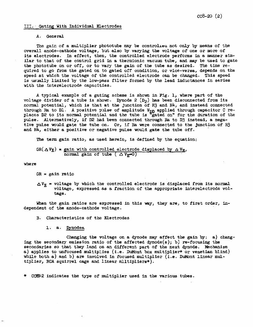
cc8-20 (2)
IIIo · Gating With Individual. Electrodes
Ao General
The gain of a multiplier phototube may be controliea not only by means of the overall anode~cathode voltage, but also by varying the voltage of one or more of its electrodeso In effect, then, the controlled electrode performs in a manner sim-ilar to that of the control grid in a thermionic vacuum tube)> and may be used to gate the phototube on or off, or to vary the gain of the tube as desiredo The time re-quired to go from the gated on to gated off condition~ or vice-versa, depends on the speed at which the voltage of the controlled electrode can be changed. This speed is usually limited by the low-pass filter formed by the lead inductances in series with the interelectrode capacitieso
A typical example of a gating scheme is shown in Fig. 1, where part of the voltage divider of a tube is showno Dynode 2 (D2) bas been disconnected from its nomal. potential, which is tbat at the junction of R3 and R4, and instead connected through Ra to Dl. A positive pulse of amplitude V~D applied through capacitor C re-places D2 to its normal potential and the tube is gated on'9 for the duration of the pulse. Alternatively, if D2 bad been connected through Ra to D3 instead, a nega-tive pulse would gate the tube on. Or, if Ra were connected to the Junction of R3 and R4, either a positive or negative pulse would gate the tube offo
where
The term gain ratio 9 as used herein, is defined by the equation~
GR( A VE) c ain with controlled electrode normal gain of tube 6 VrO
GR = gain ratio
oVE =voltage by ~hich the controlled electrode is displaced from its normal voltage)> expressed as a fraction of the appropriate interelectrode vol-tage.
When the gain ratios are expressed in this way~ they are~ to first order)> in-dependent of the anode-cathode voltage.
Bo Characteristics of the Electrodes
1. ao Dynodes.
Changing the voltage on a d;ynode may affect the gain byg a) cha.ng= 1ng the secondary emission ratio of the affected dynode(s); b) re-focusing the secondaries so that they land on an different part of the next d;ynode. Mechanism a) applies to unfocused multiplies (i.e. DuMont box multiplier* or venetian blind) while both a) and b) are involved in focused multiplier (i.e. Du.M:>nt linear mul-tiplier, RCA squirrel cage and linear mlltipliers*).
* CCBr2 indicates the type of multiplier used in the various tubes.
cc8-20 (3)
2. b. Cathode
The voltage between the cathode and focusing electrode may be con-trolled in head-on phototubes so as to cause photoelectrons to return to the cathode. The relatively high resistance of the semi-transparent cathode material in head~on tubes and the distributed capacity between the film and the glass face may slow the propagation of a gating pulse across the face of the tube unless the potential of the glass is simultaneously changed by a guard circuit.**
c. Stray Coupling
There is inevitably some capacitive or inductive electrical coupling between the gated electrode and the output electrode, represented by cD2-A in Fig. 1. This stray coupling us'IUJally amounts to from a few tenths to a few micro-microfarads, and usually results in a differentiated version of the gating signal appearing in the output. The spurious signal may be cancelled by deliberately introducing signals of the opposite polarity into the output circuitry.
Experience indicates that the 6810 is one of the better tubes for gating service, .having less stray coupling than most tube types, and is capable of giving high gain ratios.
III. Gain Ratios* of Various Tubes
Because of the large number of ways tubes may be gated, no attempt is made to present all the possible ways. Rather) the available data,.ha.s been collected in sufficient quantity to indicate a reasonable method of gating each of the tube types listed.
A. RCA Squirrel-Cage Multiplier Types
1. Nine stage.types: 1P21, 1P28, 931, etc.
a) JJynode: Typical dynode characteristics are shown in Fig. 2. A gain ratio of lo-2 is obtained with one inter-dynode displacement (i.e. Dn connect-ed to Dn-1 or Dn+l). When two dynodes are gated simultaneously, the overall gain ratio is not the product of the individual gain ratios unless the dynodes are well separated (e.g. Dl and D7, but not Dl and D3).
b) Cathode~ Displacing cathode by one inter-dynode voltage increment gives gain ratio of approximately lo-1. Displacing cathode and dynode 4 one inter-dynode voltage increment gives gain ratio of lo-3.
2. 10 stage types: 5819, 6199, 6655, etc.
a) Dynodes: See Fig. 2. Same comments as for 9 stage types.
b) Focus electrode: See Fig. 3. Photoemission of dynode 1 prevents gain ratio from being lower than about lo-3
** Fa.rinello and Ma.lvano, Rev. Sci. Instr. 29, 699, 1958. * Defined on page 2.

cc8-20 (4)
B. DuMont Box Types 6291, 6292~ 6364~ etc,
a) Dynodes: In many tubes, interdynode voltage breakdown may occur at voltage displacements of > 150 volts. Fig. 4.
b) Shield (focus electrode)~ See Fig. 5 for 6364. Photoemission from dynode 1 gives lower limit to ga.in ratio of about lo-4. Many 6292 shields ex-perience voltage breakdo...m before gain is reduced by factor of 10.
C. RCA Linear Multiplier 6810, 7046 3 7264, C7232 etc.
a) Dynodes: See Fig. 6. When several dynodes controlled, gain rati.os are multiplicative if controlled dynodes are all odd or all even-numbered.
IV. Circuitry
A pulse which is intended to gate on a normally-off phototube should have its amplitude regulated in proportion to the phototube supply voltage in order to always have the controlled electrode at the optimum voltage during the on period. Two circuits to accomplish this are given in Fig. 7 and 8.
In Fig. 7, the transistor is cut-off by the posdtive gate pulse at PG-1. Point A then initially jumps negative by Rc/Rb+Rc x supply voltage, If the time constant RbC2 is chosen to be approximately equal to Cl/2 Ra, the rate of change of voltage across C2 will c.ancel the rate of change of voltage across the c1vs. (See Waveforms.) Rise and fall times of about 0.1 microsec. can be achieved with 2N247 transistors,
Wh.ere the gate lengths are such that the size of the coupling capacitors Cl becomes unwieldy 3 a scheme such as is in Fig. 8 may be useful. Here the bistable circuit draw its operating power from the divider string. Short pulses at PG-1 alternately turn the phototube on and off.
·----8 I I
CC8-20 (5) Cathod<1.
Di
on JI node
J:t'ig. 1 - Simplified ischemb.tlc of 6ated pb0tutube Jn which the put..ential oi' dynode 2 is cunLrulled. 'J.'he tulJe :L:... ,~ated on during tne positive pulse.
I
1cr' Thig lio<i k i$ ,,,o e., ~Ol'IOUrlc..ed I ,, ,r-;,.-1---+---\---I------+---~
~me d':)"t>d'!. a..a 1
lllQ '1 ltGC<.A f' cd 11 j
,di: +I 1 riAteo4 .-- ~
--(-1 Dn-t
6AIN /O~t--~~-+-~~-i!O~~~~~
RATI0-
6R
!ds..._ ____ ~.__----~-------4--------+------.....L..----~~ -3 -2 -/ 0 I 2
(l/D,,-1) (l/V"t 1) tt;VDn- Di~p/o,:en-eni o~ ol'-j•1c:id~ n
3
V V1 .6 D,,-= -V
2..
Fig. 2 - Typical d.Ynode gati~ cnaracteristic of RCA squirrel-cage multipliers (1P2l, 931, 5819, 6342, 6655, etc.)

CCS-20 ( 6) I ... --~
i------ I !---·-----~,-.--
I I I
I -6/llN !?.I/TIO·
---~·--1 i
!
) I I
6R i /tr3 ---+-
I
I j
! Da~ +it.l:::t.11 1JJ 1 -Hi Vi ... 2oov.
j l l 1crt
10-s -/ o I
.6Vff - Di5plac.ement of foCM~ electrode.
Fig. 3 - T,ypical focus electrode gating characteristic of a head-on photo-tube with squirrel cage multiplier ()819,. 6655, 6199, etc.)
I
10· 1
f V2 -
;0-2 -· t+ V2 1+
10-3
Data.. + ... l'jf,. o.+ V ::. 1z.s 11.
3
1<-.ig. 4 - 'I'ypical dynode gating cnaracteristic of DuMont box-type multipliers (62~1, 6292, 6364, etc.)
Dn-1
Dn+1
CiAIN F?ATIO
GR
I
/(f I
10· 2.
J 10·
-~
,--! 10
·-(
'
____,-
Do.ia. ~~e" Q.t Iii.: Z~O\f,
I l I ~ O I ~'l.s - Dis-pkl.cernenf' of shield
Fig. 5 ~ Typical shield gating characteristic of 6364.
I
10·5 ------+-__ _... ____ .Ao.-. __ _._ ________ ___.
-3 -2. .. , 0 I-/ 2 (On~) ( Dn-+1')
6VDri - Dispuce111e."'t oF d'!flode Vl
CCS-20 (7)
- v, + C,oJftoekl
.,__tU1'1t-- - - - Shie.\d
,/ v. AvDn~ -Vi..
DI
02
Fig. 6 - Typical dynode gating characteristic of RCA linear multiplier (6810 1
7046, 7264, 726~, 7326, (11.232, etc.)
Prrt
0J
@_]
008-20 (8)
-L C:O.fll:
R, H.V.Su.pply --- Foe..
€4'. +l Rb R1
I 01
I - R, . C..n~'cl
02. d'l"ode
R4
Re c, 03
r- c, Czl A (I on
-t~·-Wave~ rrn~
Pr?·! £ia7'11 1,,pur
Fig. 7 - Transistor gate circuit in which magnitude of gate vo.ltage is a wroportion of the supply voltage.
--------~
E]~:11 L_-3,11 I
.l.
Fig. b - A circuit alternate to that of Fig. 7, ei;pecie.l.ly adapt,able to long gatill8 times.
Lawrence Radiation Laboratory University of California, Berkeley
File No. CC8-JO Page 1
COUNTING NOTE
A GENERATOR OF FAST-RISING LIGHT PULSES FOR PHOTOTUBE TESTING
January 21, 1959 Q. A. Kerns F. A. Kirsten G. c. Cox
ABSTRACT: The UCRL light-pulse generator provides flashes of light accompanied by electrical pulses generated at an impedance level of 50 ohms. The usual repetition rate is 60 per second. The light pulse rises and then falls to 50% peak amplitude in less than 1.5 x lo•9 seconds. The time relation between the light and electrical pulses is fixed.
Time resolution of lo·lO second is typical of measurements made with this light pulser, using conventional fast oscilloscopes (e.g. Tektronix 517), while elabora-tion of technique permits relative time measurements that are better in some cases by at least three orders of magnitude.
The light is emitted from a region a few mils in diameter, and thus may often be considered to come from a point source. The maximum light amplitude is great enough to current-saturate low-gain multipliers, or it may be so reduced as to re-lease an average of one photoelectron or less per pulse from a photocathode.
In conjunction with an oscilloscope, the lightr-pulse generator has proved use-ful in testing and evaluating the high-speed aspects of light-sensitive devices. These devices include multiplier phototubes used in scintillation and Cherenkov counters and in coincidence detectors, and low-light-level image tubes. With this pulser, tests and measurements of afterpulsing, transit time, multiplier transit.-time spread, cathode transi t•time spread, multi plier current saturation, pulse gain, etc. , can be made. A photograph of the light pulser is shown in Figure l.
OPERATING SPECIFICATIONS:
Outputs: 1. Light pulses
(a) The 10 to 90% rise time is less than 5 x lo·lO seconds. (b) They rise and then fall to 50% of peak amplitude in less than
1.5 x 10•9 seconds. (e) Light is emitted from a region a few mils in diameter. (d) Light intensity is adjustable with an attenuation ratio of ap-
proximately 100 to l without disturbing a:ny electrical settings, by means of a Polaroid attenuator •
(e) Li~ht intensity is adjustable with a ratio of approximately 10 to l by changing the applied voltage.
2. Electrical pulses (a) The electrical pulse is g~nerated simultaneously with the
light pulse, therefore can be used as a time reference for the light pulse•
(b) The 10 to 90% rise time is less than 5 x lo-lO seconds. (c) There is one monitor•signal, two 52 ohm trigger outputs, and
one 125 ohm trigger output.
Repetition Rate: Usually 60 per second, although it may be operated at rates of O to 100 per second.
File No. CCS-30 (2)
Power Requirements: 1.. A high voltage supply, adjustable from 100 to 5000 volts de. Current
drain is less than 20 microamperes~ Either polarity is permissible. The polarity of the electrical trigger pulses will be the same as the polarity of this supplyo ·
2. An adjustable source of about 3 volts at half an ampere at 60 cps for the driving coil.
A suitable supply containing both of these power sources is shown in Figure 4.
Operating Position: Vertical, with FG-5 and PG-6 up, and PG-1, PG-2, PG-3, and PG-4, down.
Opera ting Environment~ Operates most satisfactorily in a region free from strong magnetic fields or mechanical vibrations.
The temperature of the capsule enclosure should not exceed 150 degrees F.
LIGHT AND ELECTRICAL PULSE GENERATION~ The light pulses are produced in a mercury-wetted-contact relay capsule such as is used in Clare HG 1003 relays (Clare type RP-5480). The source of light is the arc formed at the contacts of the capsule. The magnetic field of a driving loop actuates the switch oontact. The contacts are normally open and when driven toward the closed posi tiO"n w1 th voltage applied, an arc forms, producing the lighto The re.sulting electrical pulse .is ,propagated down the transmission line~ GH, (Figure 2) to the resistive attenuators at Plugs 1, 2, and 4o
Energy for both the light pulse and the electrical trigger pulse is stored in the capacitance of the stationary contact of S-1 and the short lead of the 500-megohm resistor~ R-13, as indicated by DE in Figure 2.
The pulse data given for both light and electrical pulses refer to the first or primary pulse in the group. Below about 1 kv ~ usually only the primary pulse occurs. Above this voltage a group of light and electrical pulses is produced on each mechanical cycle.
The secon~ pulse of the group is delayed 2 microseconds or more after the first pulse, and may be used to trigger separate oscilloscope sweeps. The groups have been used in various ways in conjunction with a"llXiliary circuits to form gates, etc. Alternatively all signals after those derived from the first pulse may be gated out.
TR!GGER PULSE: Figure 5 shows the trigger pulse from PG-1, PG-2, or PG-4 as viewed on a 5XP11 cathode-ray tube adapted for coaxial cable connections direct to the vertical plates. The pulse has been delayed through 110 x lo-9 seconds of RG 63/u. The actual trigger pulse is shorter and higher than Figure 5 would indicate. Figure 6 gives the measured peak voltage of the trigger pulse as a function of the high-voltage power-supply setting. This setting for Figure 5 is 2400 volts. The actual peak pulse voltage for Figure 5 is about 40 volts, whereas the scope picture (which is a.J.most the impulse response of the scope) indicates about one-fifth this amplitude and a broader pulse.
The trigger pulse is short enough so that its amplitude decays to1about 1/2 the initial amplitude after traversing 100 ft of RG-9/u coaxial cable.
File No. GC8-JO (3)
i.ior~ITOR ;.;>IGN.tU.: The signal at FG-5 is the output of a capacity divider which con-sists of the 0.002?lf capacitor (C-1 of Figure 3) and the capacity (apJ;roximately 0.1 J.>Uf) between the unshielded end of the cable attached to lG-5 and the energy storage circuit, DE of Figure 2, which is not accessible otherwise. 'lhe ratio of the divider is thus about 0.1.JJ,Uf divided by 0.002).lf, or 1:20,000 for an open circuit at PG-5. Gate signals required to occur a few microseconds or less in advance of the light pulse can be generated from the monitor signal.4
LIGET OUTPUT: Figure 7 shows the light output in terms of the response of an S-11 photocathode as a function of the high voltage for several units of the present design. Figure 8 (upper trace) shows the approximate li~ht-pulse wave shape as measured by a special phototube with control grid gated.
The spectrum of the light emitted from the pulser shows some output throughout the visible range but is predominantly in the blue region.5
The fraction of the emitted light having vertica~ polarization ranges from .6 for a 5000 volt setting to .9 for a 200 volt setting.
POLAHOID A'i'TENUA'l'OR: The light attenuator consists of a stationary and a rotatable disc of f'olaroid film, providing a way of adjusting the light amplitude. It may be attenuated by means of the adjustment handle, (E of Figure 1) by a factor of 100 over mininnm1 attenuation.
'l'YllG.AL H10TOT1JBE-TE;:>T SETUP: Figure 9 shows a typical test setup. Jeveral tubes may view the light source through various optical paths if desired. One of the trit:~ger tubes may appear as a fiducial mark on the oscilloscope sweep (Cable B) , another may be used for Li-axis modulation, etc.
Purther details on the use of the light pulser together wi tb constructional· drawing nu.11bers and accessory equipment drawings are available.3
1. UChL Counting Handbook, Counting Note CC2-l. 2. Frederick A. Kirsten, Measurement of the .Stape of the Light :r:ulse Gener-
ated by foercury Light Pulser 4V5572, Engineering Note EE548, April 1958. J. Q. A. Kerns, F. A. Kirsten, G. C. Cox, A Generator of Fast-Rising Light
Pulses for Fhototube Testing. UCRL-8227, i'ltarch 1958. 4. San~e, l;age 15. 5. Same, Fage 27. 6. Same, Page 26.
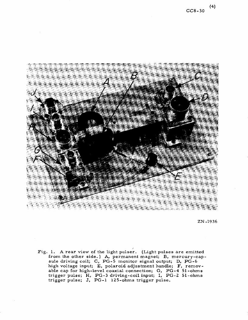
(4) CCB-30
ZN -1936
Fig. 1. A rear view of the light pulser. (Light pulses are emitted from the other side.) A, permanent magnet; B, mercury-cap-sule driving coil; C, PG-5 monitor signal output; D, PG-6 high voltage input; E, polaroid adjustment handle; F, remov-able cap for high-level coaxial connection; G, PG-4 51-ohms trigger pulse; H, PG-3 driving-coil input; I, PG-2 51-ohms trigger pulse; J, PG-1 125-ohms trigger pulse.
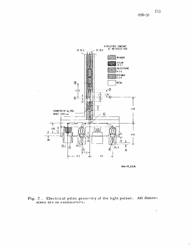
K•OIELECTRIC CONSTANT TO PG-5 .--- TO PG-C AT 1or CYCLES /SEC .
®r 3 .0 5
(DL-=t 25
DIAMETER OF H, POOL "'I. . ABOUT 0 64 cm. --- -- - ~ ~'-
1.95 __ L_ j _lj_.
-r-----.60
---- -------- \
...... ~MERCURY
TEFLON K" 2 I
POLYSTYRENE M.5
~BEESWAX ~M4
DMETAL
--------T(D ·-----,-·--1.0 1pfi'\
-----~------w-·-----···--· -I 0 __ L
-T-·-···1_ __
- -®
4 5
5.02
MU-15,266
(5) cc8-30
Fig. 2 . Electrical pulse geometry of the light pulser. All dimen-sions are in centimeters.
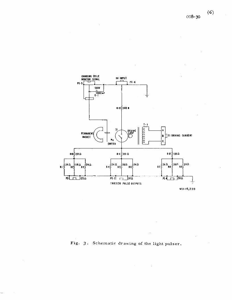
R-1
ccB-30
CHARCINC CYtlE HV INPUT MONITOR SIGNAL ,--=.-
PC-5 Tu-_L.___~-6 SOOY --i
002onf l C-1 -=-
R-13 500 II
T- I
PERllANENTr? NACUT \S
H9 SWITCH
WTI "'"" "'"" A-II 130 Sl R-12 130Sl
24Sl R-4
·~---~~' :·~·:~t· J TRICCER PULSE OUTPUTS
MU-15,239
Fig. 3. Schematic drawing oft.he light. pulser.
(6)
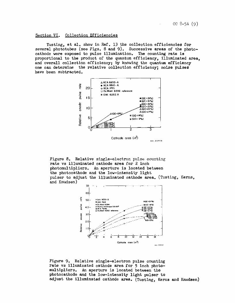
CC 8-5A (9)
Section VI. Collection Efficiencies
Tusting, et al, show in Ref, 13 the collection efficiencies for several phototubes (see Figs, 8 and 9). Successive areas of the photo-cathode were exposed to pulse illumination. The counting rate is proportional to the product of the quantum efficiency, illuminated area, and overall collection efficiency; by knowing the quantum efficiency one can determine the relative collection efficiency; noise pulses have been subtracted,
Q)
~ 20 Q) (/)
:J 15 a. Q)
"t:l 0 10 c: 0
Q) > 5 0 a; 0:
00
A RCA 6655-A e RCA 6810-A o RCA IP21 o Du Mont 6292 reference
* EMI 6262 A e(QE=19%) e(QE=19%) elQE=19%)
(QE=15%) A(QE=l4%) A(QE=17%)
*lQE=l4%) *(QE• 9%)
2 3
Cathode area (irf.l MU-25908
Figure 8. Relative single-electron pulse counting rate vs illuminated cathode area for 2 inch photomultipliers. An aperture is located between the photocathode and the low-intensity light pulser to adjust the illuminated cathode area, (Tustlng, Kerns, and Knudsen)
6.0.
~ -;; 4.0 Q.
~ 3.0 0 c: 0
2.0
oEMI 9~30-B +ces 7819 O(QE•23%)
10 12 14 16 18
Cathode area (in2 ) MU·15f0f
Figure 9. Relative single-electron pulse counting rate vs illuminated cathode area for 5 inch photo-mul tipliers. An aperture is located between the photocathode and the low-intensity light pulser to adjust the illuminated cathode area. (Tusting, Kerns and Knudsen)
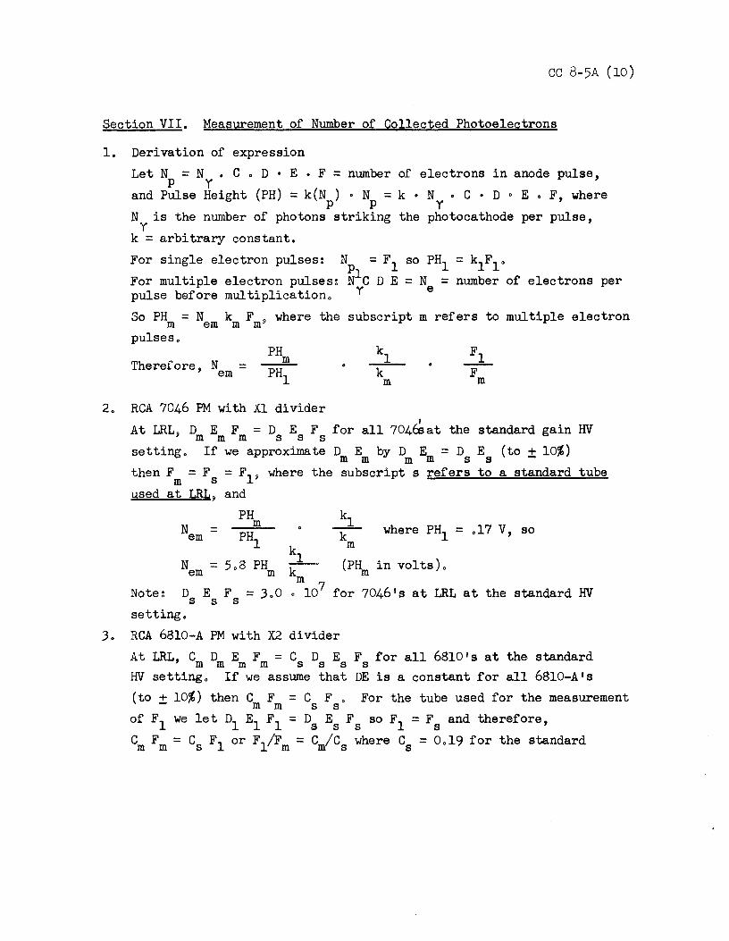
CC 8-5A (10)
Section VII. Measurement of Number of Collected Photoelectrons
1. Derivation of expression Let N = N • C • D • E • F = number of electrons in anode pulse, p y and Pulse Height (PH) = k(N ) • N = k • N • C • D • E • F, where p p y
number of photons striking the photocathode per pulse, N is the y k = arbitrary constant. For single electron pulses: For multiple electron pulses~ pulse before multiplication.
N = F1 so PH1 = k1F1 • P1 N C D E = N = number of electrons per
Y e
So PH = N k F 9 where the subscript m refers to multiple electron m em m m pulses.
Therefore, N = em
2. RCA 7046 PM with Xl divider
3.
I At LRLj D E F = D E F for all 704tsat the standard gain HV m m m s s s setting. If we approximate D E by D E = D E (to ± 10%) m m m m s s then F = F = F1 ~ where the subscript s refers to a standard tube m s used at LRLj and
N = em PH m ~ k where PH1 = .17 V, so
m
N = 5.8 PH em m (PHm in volts).
Note~ D E F = 3.0 s s s for 7046's at LRL at the standard HV setting. RCA 6810-A PM with X2 divider At LRL, C D E F = C D E m m m m s s s HV setting. If we assume that (to + 10%) then C F = C F • - m m s s
F for all 6810 1 s at the standard s DE is a constant for all 6810-A's For the tube used for the measurement
of F1 we let D1 E1 F1 = D8 Es Fs so F1 = Fs and therefore, C F = C F1 or F1/F = C /C where C = 0.19 for the standard mm s m ms s
4.
tubep so
N em PH m
Now PH1 = 0.076 V, so k
N = 69 (PH ) • (Cm) • k:::l • em m (PH in V m m
Measurement of Pulse Height C in decimals) m
(PH).
CC 8-5A (11)
Using the ~roper phototube divider, the anode signal (not back terminated) was fed through a short length of RG 63/u 125 Q cable into a Tektronix B 170-A, 170 Q scope attenuator in parallel with 470 Q to ground. In both cases the phototube HV was set such that the quantity D • E • F (de gain) was equal to 3.0 x 10⁷. The Tektronix 517 A scope w~s calibrated on the 0.5 V (10 Q) scale at 1/5 full scale using the 170 Q signal cable directly from calibration output to signal input. The sensitivity with no attenuation was then 0.10 V/cm. Any further attenuation should be obtained from the 170 Q attenuator box. The scope trigger was obtained from the Hg pulser light source used to obtain the single photoelectrons. The light repetition rate was 60 per second and the intensity was attenuated until only approximately 6 pulses per second were detected. In this condition only 1/20 of the pulses were due to 2 or more photoelectrons. The values given for PH1 in section 2 and 3 have been corrected for multiple electron pulses. The factor of 2 difference from 6810 A to 7046 PH1 is a reflection of the lower collection efficiency of the 7046. The assumption is made in this measuring technique that there is no contribution to many electron pulse heights from very small but numerous pulses which would have been invisible in the ab~ve method.
5. Measurement of k1/km.
A rough determination of k1/km was made under the assumption that the charge contained in an anode pulse is proportional to the product of PH and full width at half maximum. The values for the RCA 6810 A are:
PH number of e kl/km
.076 v 1 1.00 2.82 v 37 1.46
and for the RCA 7046
PH number of e kl/km
.173 v 1 1.00 3.6 v 21 1.27
Radiation Laboratory, University of California, Berkeley
COUNTING NOTE
ELECTRICAL GATING OF MULTIPLIER PHOTOTUBES
I. Introduction:
File No. CC8-20 Page l December 29 ,· 1958 F. Kirsten
Several use:f'ul. methods of gating multiplier phototubes are available. This note is primarily concerned with gating by means of controlling the voltages on the phototube electrodes. Several advantages of this method make it attractive for ma.Dy applications:
(l) A relatively high speed - most tubes may be turned on or off in a few nano-seconds with appropriate circuitry. This permits using the pbetotubes as coincidence detectors in some applications.
(2) Very small ratios of off-to-on gain can be achieved. For example, control-ling three dynodes in a 6810 gives a gain ratio of < io-6, and much smaller ratios are easily available.
(3) Light-or ion-feedback afterpulsing induced by large unwanted light pulses may be eliminated. This is especially usef'Ul. where one desires to detect a small light signal following a much larger light signal. Under some conditions, after-pulsing following the large signal might obscure the small one, unless the larger were gated out. Note that gates following the phototube will not remove the after-pulsing.
II. High-Voltage Supp!y Control
The method of gating by turning the supply voltage on and off has been used* and is quite usef'Ul. in some cases. It bas, however, several disadvantages: (a) Where capacitors of unequal value are used across voltage-divider resistors, the quiescent voltage distribution is not achieved until all capacitors have charged. In general, the gain of the tube will not be constant during the charging time. (b) Excess noise (i.e. light) is genera·ted when charging currents are required to flow on insulating surfaces such as the glass envelope. This excess noise dies down with a time con-stant characteristic of the particular tube after the voltages have been changed.
This method also bas an advantageous feature, in common with the method in Sec. III below. Owing to light feedback and other regenerative process, in most tubes there is found, as the supply voltage is raised, a maximum usable gain, above which the anode dark-current increases spontaneously until limited by the voltage divider. The time required tor regeneration to build up amounts to at least one transit time in the case of light feedback,** or much longer in the case of ion feedback. Thus, if the tube is gated on for the order of one transit time, a higher gain may be achieved during the on-time than if the tube is on continuously.
* Post and Shiren, Pb;ys. Rev. 78, 81, April 1950· ** The intensity of light emitted when a step of multiplier current occurs appears
to build up with a time constant of alx>ut one microsecond.

cc8-20 (2)
III. · Gating With Individual Electrodes
A. General
The gain of a multiplier phototube may be controlled not only by means of the overall anode-cathode voltage, but also by varying the voltage of one or more of its electrodeso In effect, then, the controlled electrode performs in a manner sim-ilar to that of the control grid in a thermionic vacuum tube~ and may be used to gate the phototube on or off, or to vary the gain of the tube as desired. The time re-quired to go from the gated on to gated off conditionp or vice-versa, depends on the speed at which the voltage of the controlled electrode can be cbangedo This speed is usually limited by the low-pass filter formed by the lead inductances in series with the interelectrode capacities.
A typical example of a gating scheme is shown in Fig. 1, where part of the voltage divider of a tube is shown. Dynode 2 (n2 ) has been disconnected from its non!!al potential, which is that at the junction of R3 and R4, and instead connected through Ra to Dl. A positive pulse of amplitude V~D applied through capacitor C re-places D2 to its normal potential and the tube is gated on'9 for the duration of the pulse. Alternatively, if D2 bad been connected through Ra to D3 instead, a nega-tive pulse would gate the tube on. Or, if Ra were connected to the junction of R3 and R4, either a positive or negative pulse would gate the tube off,
where
The term gain ratio~ as used herein, is defined by the equation~
GR( A VE) c ain with controlled electrode normal gain of tube 6 Vr0
GR = gain ratio
6VE = V?ltage by which the controlled electrode is displaced from its normal voltage~ expressed as a fraction of the appropriate interelectrode vol-tage.
When the gain ratios are expressed in this wayp they are~ to first order, in-dependent of the anode-cathode voltageo
Bo Characteristics of the Electrodes
lo a. o Pynodes.
Changing the voltage on a dynode may affect the gain by~ a) chang= ing the secondary emission ratio of the affected dynode(s); b) re-focusing the secondaries so that they land on an different part of the next dynode. Mechanism a) applies to unfocused multiplies (i.e. DuMont box multiplier* or venetian blind) while both a) and b) are involved in focused multiplier (Le. DuM:>nt linear mul-tiplier, RCA squirrel cage and linear mlltipliers*)o
* CC8f2 indicates the type of multiplier used in the various tubes.
cc8-20 (3)
2. b. Cathode
The voltage between the cathode and focusing electrode may be con-trolled in head-on phototubes so as to cause photoelectrons to return to the cathode. The relatively high resistance of the semi-transparent cathode material in head-on tubes and the distributed capacity between the film and the glass face may slow the propagation of a gating pulse across the face of the tube unless the potential of the glass is simultaneously changed by a guard circuit.**
C. Stray Coupling
There is inevitably some capacitive or inductive electrical coupling between the gated electrode and the output electrode, represented by CD2-A in Fig. l. This stray coupling us1Ulal.ly amounts to from a few tenths to a few micro-microfarads, and usually results in a differentiated version of the gating signal appearing in the output. The spurious signal may be cancelled by deliberately introducing signals of the opppsite polarity into the output circuitry.
Experience indicates that the 6810 is one of the better tubes for gating service, having less stray coupling than most tube types, and is capable of giving high gain ratios.
III. Gain Ratios* of Various Tubes
Because of the large number of ways tubes may be gated, no attempt is made to present all the possible ways. Rather) the available data,has been collected in sufficient quantity to indicate a reasonable method of gating each of the tube types listed.
A. RCA Squirrel-Cage Multiplier Types
l. Nine stage.types: 1P2l, 1P28, 931, etc.
a) :Qynode: Typical dynode characteristics are shown in Fig. 2. A gain ratio of lo-2 is obtained with one inter-dynode displacement (i.e. Dn connect-ed to Dn•l or Dn+l). When two dynodes are gated simultaneously, the overall gain ratio is not the product of the individual gain ratios unless the dynodes are well separated (e.g. Dl and D7, but not Dl and D3).
b) Cathode: Displacing cathode by one inter-dynode voltage increment gives gain ratio of approximately lo-1. Displacing cathode and dynode 4 one inter-dynode voltage increment gives gain ratio of lo-3.
2. 10 stage types: 5819, 6199, 6655, etc.
a) Dynodes: See Fig. 2. Sa.Ine comments as for 9 stage types.
b) Focus electrode: See Fig. 3. Photoemission of dynode 1 prevents gain ratio from being lower than about lo-3.
** Farinello and .Malvano, Rev. Sci. Instr. 29, 699, 1958. * Defined on page 2.

cc8-20 (4)
B. DuMont Box Types 6291i 6292~ 6364, etc.
a) Dynodes: In many tubes, interdynode voltage breakdown may occur at voltage displacements of > 150 volts. Fig. 4.
b) Shield (focus electrode): See Fig. 5 for 6364. Photoemission from dynode 1 gives lower limit to gain ratio of about lo-4. Many 6292 shields ex~ perience voltage breakdo"Wn before gain is reduced by factor of 10.
C. RCA Linear Multiplier 6810, 7046, 7264, C7232 etc.
a) Dynodes: See Fig. 6. When several dynodes controlled, gain ratios are multiplicative if controlled dynodes are all odd or all even-numbered.
IV. Circuitry
A pulse which is intended to gate on a normally-off phototube should have its amplitude regulated in proportion to the phototube supply voltage in order to always have the controlled electrode at the optimum voltage during the on period. Two circuits to accomplish this are given in Fig. 7 and 8.
In Fig. 7, the transistor is cut-off by the posdtive gate pulse at PG-1. Point A then initially jumps negative by Rc/Rb+Rc x supply voltage. If the time constant RbC2 is chosen to be approximately equal to Cl/2 Ra., the rate of change of voltage across C2 will cancel the rate of change of voltage across the c1vs. (See Waveforms.) Rise and fall times of about 0.1 microsec. can be achieved with 2N247 transistors.
Where the gate lengths are such that the size of the coupling capacitors Cl becomes unwieldyi a scheme such as is in Fig. 8 may be useful. Here the bistable circuit draws its operating power from the divider string. Short pulses at PG-1 alternately turn the phototube on a.::id off.

t Voo
i
E I
CCB-20 (5) CathodlJ.
I
I
01
on /,;node
ovfp""f
J:t'ig. l - Simpli:t'ied i:;chemu.tic 01' f5ated pllotutube Jn w11icll the put:,ential of dynode 2 is cunLrulled. The tutJe :i.:.; r~ated on during tne positive pulse.
I
Thig ~oti le i$ mo e 1cr' pt'0111our1c.ed I n 1 ,_ ......... t----i.--4-----4----__._---~
.some d'j"t>d'$ a>'ld 1
"'1l '1 OC:.Ct.I .,. td ,' I di= +I •ri•teo4 ~- ~
--+(-ti Dn-t
6AIN /Cflt-~~-+-~~--.i~~~-1-~
RATI0-
6R
I
1o"S .__--~---~----t-----4------'-----' -:.3 -2 -/ 0 I 2
(l/o.,_,j {Yrhit •> .t.Vpn- D1~pb.::e1·,-oer'li of- r)'-jr1c:.d~ n
3
V V1 .a D,, = -V 2..
Fig. 2 - Typical d,Ynode gati~ cnara.cteristic of RCA squirrel-cage multipliers (1P21, 931, 581~, 6342, 6655, etc.)
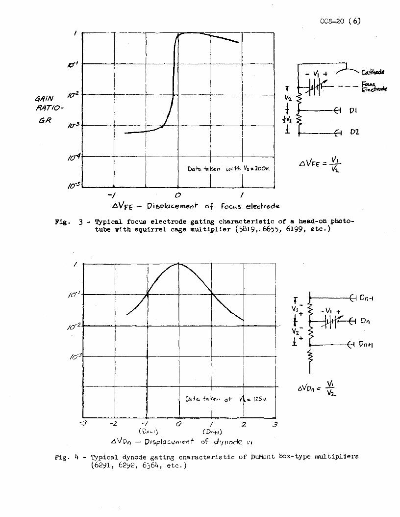
CCS-20 ( 6)
61/IN l?ATIO· 6R
I
----
i---·--I
i J i ---+-:
-~ I -----
~1-.--- Vj 4
I I
I ! I I DI
i D2
1crt t:)Q ~ +ra. ic e.11 t>J• Hi Vi .. 2oov.
10-s l l -! o I
L1Vff - D'1&plac.ement of foCM~ electrode.
Fig. 3 - Typical focus electrode gating characteristic of a head-on photo-tube with squirrel cage multiplier ()819 1 .6655, 6199, etc.)
I
10·1
f V2-t+
;0-2 . - .. Vi.-1+
10·3
-2 -/ 0 I 2 3 ( Dt>-t1)
1',ig. 4 - 'I'ypical dynode gating cnaracteristic of DuMont box-type multipliers (62~1, 6292, 6364, etc.)
DrH
Dn+r
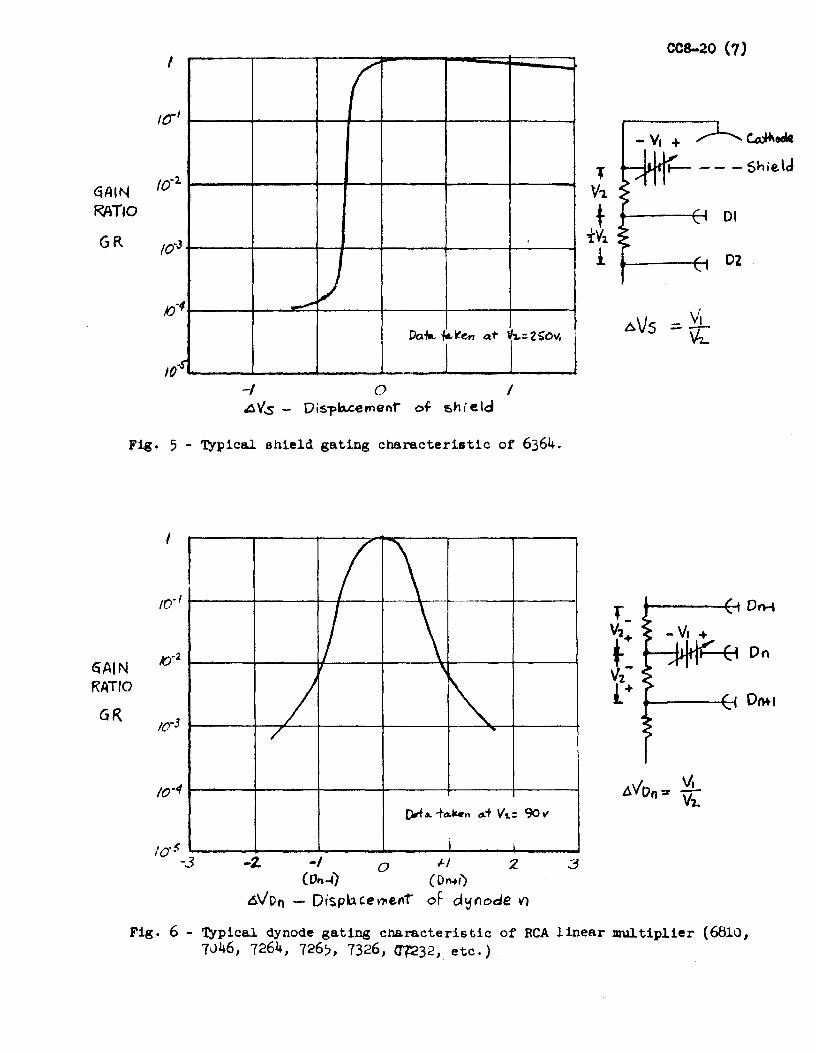
qAIN RATIO
GR
I
I
10· l
J 10·
-4
. ..r 10
·-(
'
__,,,.,. l) Do.~ .,_li.'en at Ill.: Z~C>v,
- J I I -I O I &l'ls - Dis-pb.cernent" of shield
Fig. 5 - Typical shield gating characteristic of 6364.
I
1o·S '-----+-----"---.i.-.---..i..-----__.. -3 -2. ·I o 1-1 2. (On~) ( D~1)
oVDri - Dispbce111e.nt oF dyflode VJ
CCS-20 (7)
-V1 + ~odll
--tU'I t-- - - - Shie.\d
,/ v, AVDn::r -v,_
DI
02
Fig. 6 - Typical dynode gating characteristic of RCA linear multiplier (6810, 7046, 7264, 726), 7326, ~32, etc.)

P4·1
0
@]
CC8-20 (8)
-L C.o:lltt
R, H.V.StA.pply --- Foe.
€4<.
~l Ro R'l
I DI
I - R, . c.,,,~-J
02. d'J,.ode
R4 Re c, 03
7- c, c~l A (I Dn
-tR•~ Wavefo r111~
~-I Ga'ftt ,,.,P"r
Fig. 7 - Transistor gate circuit in which magnitude of gate vo.l tage is a ~roportion of the supply volt.age.
1=3.<:11 ,., - I
I _i_
--------"*'
Fig. b - A circuit alternate to that uf Fig. 7, ei;pecie.lly adaptable to long gating times.
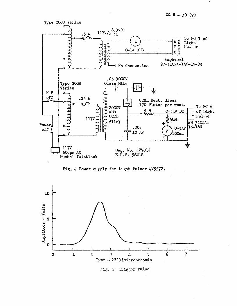
cc a - 30 (7) Type 200B Varinc
Power of£
10
., ...., .4 0
I> i ~
t>
11 ...., ..... .4 p.
!2 0
0
~
117V 60cpa AC
• 5 A
Hubbel Twistlock
ll7V /. 6.JVCT /~~ lA c----0--c 0-lA H.HS
To PG-J of Lir,ht Puloer
~ No Connection Arn.phenol
97-Jl02A-14S-1S-02
UCRL H.ect. diecs 170 Plates per reot. To PG-6
or IA1!~1t Pul1:>er
M 0-KVDC
.005 10 KV
Dwg. No. 4V7E312 E.P.S. 5S:21S
AN Jl02A-0..5KV 18-163 OOua
Fig. 4 Power supply for Light Pulser 4v5572.
1 2 J 4 5 6 7 Ti.lne - !Qllimicroscconde
Fig. 5 Trieeor Pu.16~
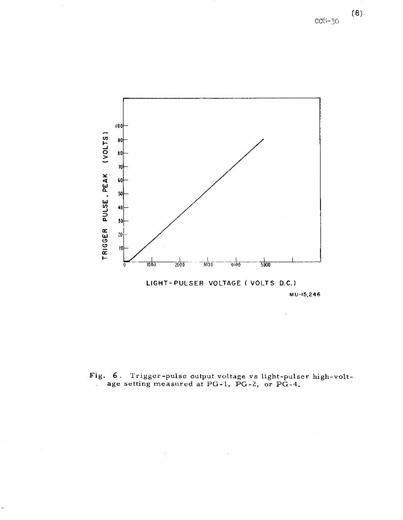
(8) ccD-30
100
en 90 t-...J 0 > 80
70 ~ <( 60 I.LI a. 50 I.LI en 40 ...J ::> a. 30 cc I.LI <.!> <.!> cc ~ __ J - -- ___ J ______ l___ __ ~--~
0 .~000 4000 5000
LIGHT-PULSER VOLTAGE (VOLTS D.C.)
MU-15,246
Fig. 6. Trigger -pulse output voltage vs light-pulser high-volt-age setting measured at PG-1, PG-2, or PG-4.
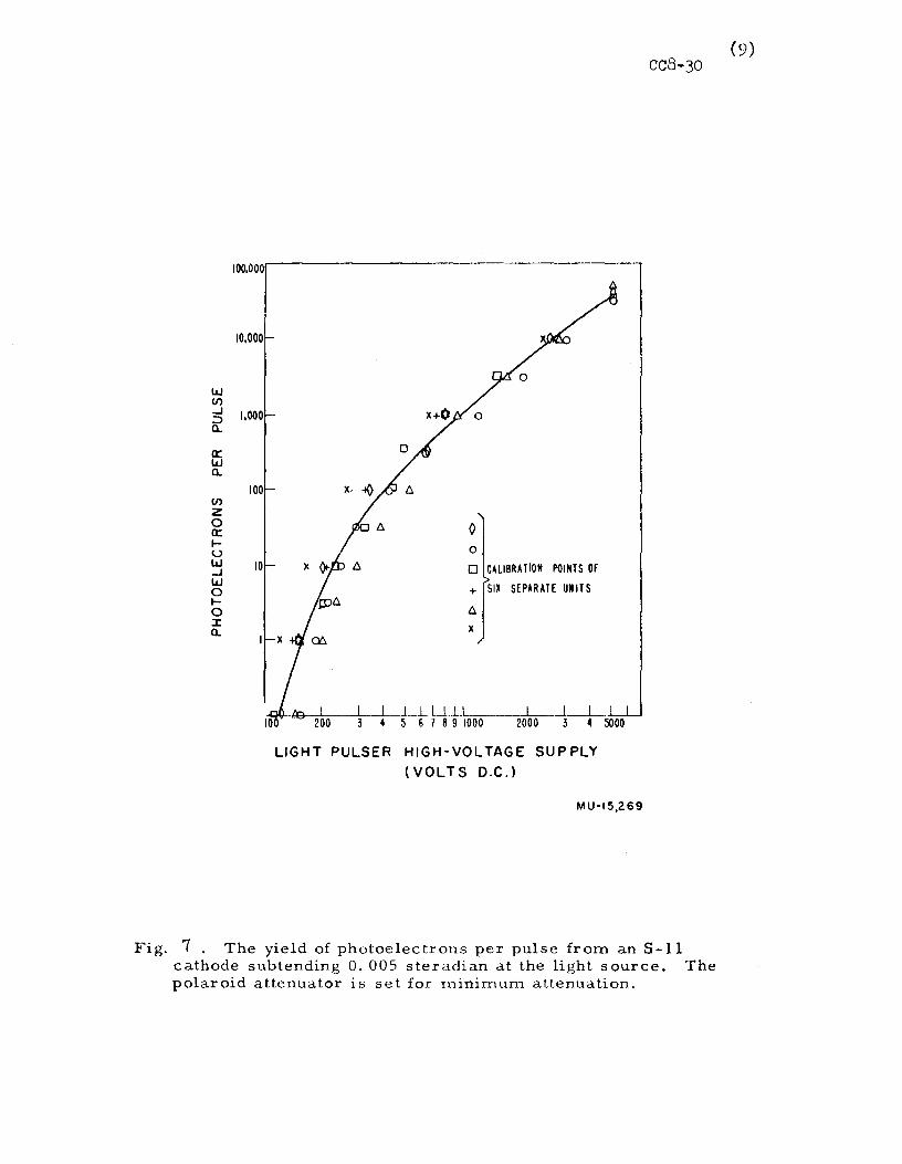
w (/) ....J ::> a_
a: w a_
(/) z 0 a: I-u w ....J w 0 I-0 :c a_
100,000
10,000
1,000 -
100
() 0
10 0 CALIBRATION POINTS OF
+ SIX SEPARATE UNITS
t:,. x
.~-"9---::-':-:--~-_l__J __ l U.lL _____ ~-~~-~~ 200 4 5 6 7 8 9 1000 2000 4 sooo
LIGHT PULSER HIGH-VOLTAGE SUPPLY (VOLTS D.C.)
MU-15,269
cc8 .. 30
Fig. 7 . The yield of photoelectrons per pulse from an S-11 cathode subtending 0. 005 steradian at the light source. The polaroid attenuator is set for n1inimum attenuation.
(9)
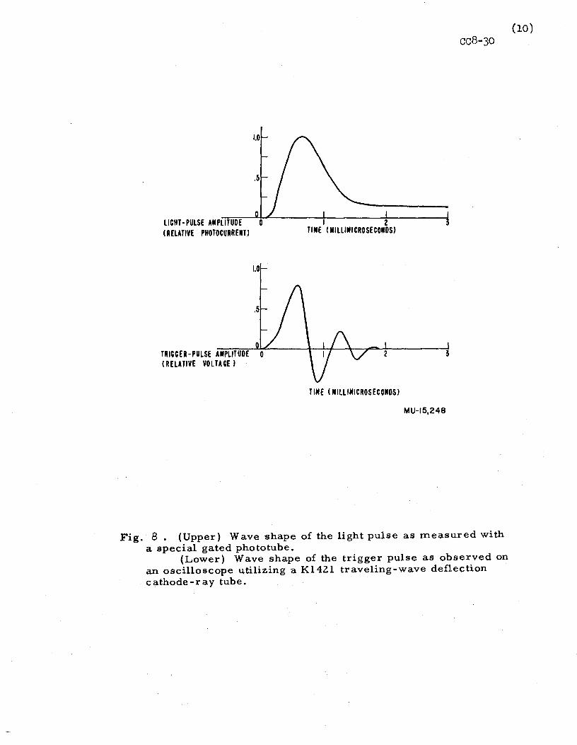
LICHT· PULSE AMPLITUDE I RELATIVE PHOTOCURRENTJ
1.0
TRICCER-PULSE AMPLITUDE 0 I RELATIVE VOLTAGE l
2 TINE ( lllLLllll CROSECONDS)
2
TIME ( NILLIMICROSECONDSl
cc8-30
3
MU-15,248
Fig. 8 . (Upper) Wave shape of the light pulse as measured with a special gated phototube.
(Lower) Wave shape of the trigger pulse as observed on an oscilloscope utilizing a Kl42.l traveling-wave deflection cathode-ray tube.
(10)
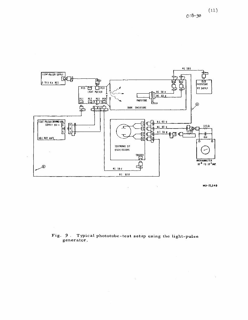
LICHT-PULSER SUPPLY
0 TO 5 KV REC_
ADJ REP. RATE
_/_r' ~ ......... ~_,..-_....--..... '-~
PHOTO TUBE
DARK ENCLOSURE
TEKTRONIX 511 OSCILLOSCOPE
RC 58 U
RC 63 U
R.C. 63 U
cc8-30
PHOTO TUBE HY. SUPPLY
(ll)
MICR OAMM E TE R 10- 8 TO 10'3 AMP.
MU-15,249
Fig. 9 . Typical phototube-test setup using the light-pulse generator.
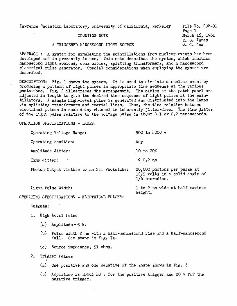
Lawrence Radiation Laboratory, University of California, Berkeley File Noo CC8-31 Page 1
COUNTING NOTE
A TRIGGERED NANOSECOND LIGHT SOURCE
March 16, 1961 To G. Innes G. Co Cox
ABSTRACT : A system for simulating the scintillations from nuclear events has been developed and is presently in use. This note describes the system, which includes nanosecond light sources, coax cables, splitting transformers, and a nanosecond electrical pulse generatoro Special considerations when employing the system are describedo
DESCRIPTION: Fig. 1 shows the system. It is used to simulate a nuclear event by producing a pattern of light pulses in appropriate time sequence at the various phototubeso Fig. 2 illustrates the arrangement. The cables at the patch panel are adjusted in length to give the desired time sequence of light pulses at the scin-tillatorso A single high-level pulse is generated and distributed into the lamps via splitting transformers and coaxial lines. Thus, the time relation between electrical pulses in each delay channel is inherently jitter-free. The time jitter of the light pulse relative to the voltage pulse is about Ool or 0.2 nanoseconds.
OPERATION SPECIFICATIONS - LAMPS:
Operating Voltage Range:
Operating Position:
Amplitude Jitter:
Time Jitter:
Photon Output Visible to an Sll Phototube:
Light Pulse Width:
OPERATING SPECIFICATIONS - ELECTRICAL PULSER:
Outputs:
1. High Level Pulse
(a) Ampli tude..--J kv
500 to 4000 v
Any
10 to 20%
201 000 photons per pulse at 1275 volts in a solid angle of 1/6 steradian ..
1 to 2 ns wide at half maximum heigh to
(b) Pulse width 2 ns with a half-nanosecond rise and a half-nanosecond fall. See shape in Fig. 7a.
(c) Source impedance, 51 ohms.
2o Trigger Pulses
(a) One positive and one negative of the shape shown in Figo 8
(b) Amplitude is about 40 v for the positive trigger and 20 v for the negative triggero

File Noo CCB-31(2)
Repetition Rateg
The adjustment range is 70 to 150 pps, usually set to 100 pps by front panel screwdriver adjustmento This is the repetition rate at which the panel voltmeter is calibratedo
Power Requirements~
Operating Position~
Usually vertical, (any position that keeps the contacts from becoming bridged by the contained mercury is satisfactory)o
Operating Environment~
Free from strong mechanical vibrations and strong magnetic fields (shaking of the mercury surface on the pulse generating gap increases the pulse height jitter) o
Pulse Height Stabilityg
Pulse to pulse jitter is less than 5%o There are long-term drifts which can be corrected using the front panel meter. as a relative indicator of pulse heighto Pulse heights can be re-established to within t 3%o (See section on "Electrical Pulse Operation".)
BARIUM TITANATE LAMPSg A small pulsed-light source has been developed using field-emitted electrons to initiate a discharge in hydrogen. 'Ihe discharge is obtained by applying a voltage to the junction of a tungsten wire and a dielectric, in this case a barium-titanate ceramic. 'Ibis ceramic exhibits a high dielectric con-stant~ typically greater than 40000 The voltage is generated by the 3-kv nanosecond pulse generator, which will be described later. The lamp is shown in Fig. 3o
The tungsten lead is grounded and a positive pulse is applied to the titanateo This results in electrons being emitted from the tungsten due to the high field concentration at the junctiono Ari avalanche is started in the hydrogen and con-tributes to the total current through the device. The gas pressure is 1/2 atmos-phere9 hence, the avalanche is quickly quenched upon removal of the electrical pulseo The light. pulse is 1 to 2 nanoseconds in length.
Figo 4 shows the electrical output from a 1P21 multiplier phototube when illumina-ted with the lamp. 'lhe photo was taken from a HP-185A sampling oscilloscope. The phototube is not saturatedo Fig. 5 shows samples of seven lamps operating under identical conditions of pulse voltage. 'lhe phototube voltage is held constant. Four lamps have about 20% amplitude difference while lamps 4 and 5 have a factor of 2 greater outputo Lamp 2 is an old style and would not be used in a system comprised of the other sixo 'lhese figures represent about 20,000 photoelectrons incident on the photocathodeo
The operating voltage range extends from 500 to }¥:00 volts. The best operating range in terms of amplitude stability and time jitter is at the higher voltageso Amplitude jitter is on the order of 10 to 20% more than one would estimate from the photon statistics aloneo
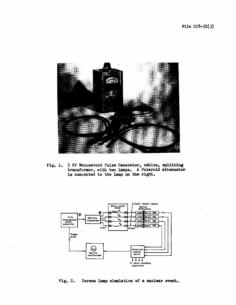
File cc8-3l(J)
Fig. 1. 3 KV Nanosecond Pulse Generator, cables, splitting trans.former, with two lamps. A Polaroid attenuator is connected to the lamp on the right.
3-k• Nano11cond
pul11 a•n•rator
Trl991r pulH
Spllttln9 tran1former
g Monitor
01cl1101cape
Equal len9th cablH
a~f~~cu°c:tor1
Phototube ------' --------1 monitor board
To data-recording apparatus
Corona lamp simulation o.f a nuclear event.
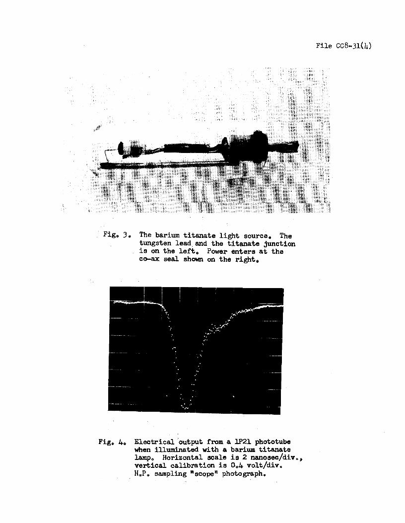
Figo 3. The barium titanate light source. The tungsten lead.and the titanate junction is on the lefto Power enters at the co-ax seal shown on the right 0
Figo 40 Electrical output from a 1P21 phototube when illuminated with a barium titanate lampo Horizontal scale is 2 nanosec/div o, vertical calibration is 0.4 volt/divo HoPo sampling ttscope" photograph.
File ccB-31(4)
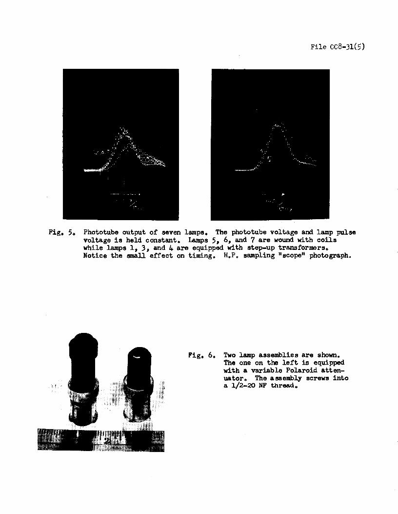
File ccB-31(5)
Fig. 5o Phototube output of seven lamps. The phototube voltage and lamp pulse voltage is held constant. Lamps 5, 6, and 7 are wound with coils while lamps 1, 3, and 4 are equipped with step-up transformerso Notice the small effect on tim.i.ngo HoPo sampling "scope" photograph.
Fig. 60 Two lamp assemblies are shown. The one on the left is equipped with a variable Polaroid atten-uator o The assembly screws into a 1/2-20 NF threado

File Noo CC8-31(6)
OPTICAL ATTENUATOHS ~ Optimum light levels for a particular phototube can be achieved by optical attenuationo Pieces of film or drafting tape can be usedo In Figo 6!1 a variable optical attenuator is showno. This attenuator provides adjust-ment of the light amplitude without disturbing any of the electrical settingso An adjusting ring moves an inner Polaroid film with respect to the outer Polaroid film and the lampo Indexing lines are spaced to give attenuation steps of two up to an attenuation factor of 640 Stops are at minimum and maximum attenuationo The maximum is greater than lOOX the minimumo
Drafting tape is an economical attenuatoro One layer of tape corresponds to a loss of about 50Xo In quantities of one to five, the variable optical attenuator requires one day of shop time to fabricateo If sufficient interest is shown in the variable attenuator, to justify making a large number, the price per unit would be reasonable 11 about that of a 125 ohm connector. It should be kept 'in mind that the added cost of a variable attenuator may be justified in terms of the added flexibili tyo
LIMITATIONS IN TI:fE: NUMBER OF LAMPS: The attenuation of the cables used to connect the lamps will limit the number of lamps that can be run in a single arrayo The amplitude and time jitter one can tolerate is a factor one must considero The lamps have a threshold or minimum voltage necessary to initiate the discharge. In order to insure a discharge with minimum amplitude and time fluctuations, a high-amplitude fast-rise pulse must be used. Pulse amplitude of two times threshold is adequate. Therefore, attenuation introduced by cables must be considered along with distortion of the pulseo The distortion will slow the rate of rise of the voltageo Threshold voltages vary from 300 to 500 voltso Consequently, cable runs of several feet will allow one to use two splitting transformers for a total of sixteen lampso When enough cable is used to introduce 4 to 6·db loss11 (lo6 to 2X loss) only one splitting transformer should be usedo A long cable with 10 to 12-db ( 3 to 4 times loss) attenuation will light one lampo However, it should be kept in mind that the number of lamps and cable lengths are dependent upon the requirements of the experimento Over 100 lamps can be pulsed in a single array if one can tolerate the amplitude jittero
A step-up transformer is usually packaged with the lampo 'Ibis will double the voltage at the lamp, thereby increasing the number of lamps lit in any arrayo 1he effect upon timing is small. In Figo 5 lamps 1, 3, and 4 have transformers, while 511 6, and 7 are wound with peaking coilso
Better performance is obtained with a step-up transformer than with a coilo The step-up transformer will, therefore, be offered as an optiono 'Ihe transformers (or coils) will slow the rise time of the applied voltage 10 to 20%0 This will add to the time jitter of the light pulseo The amount of time jitter of the light may not be as important as the amplitude jitter of the light. Vfuere cable loss is a factor and/or a large number of lamps are to be lit by a single electrical pulse, the transformer should be included. Amplitude jitter of the lamps will generally cause time jitter in the electronics that follow. Again, it must be stressed that the optimum combination of lamps:J transforrners 9 and cables will be dependent upon the requirements of the experimento Lamps with transformers will be color-coded red when viewed from the end with the GR connector.,
If the applied voltage to the lamp is increased indefinitely, arcing occurs in the lampo If only one lamp is to be used9 a 6.-db pad (2X loss) or splitting trans-former should be in series with the lampo 1be lamps are terminated by 51 ohms inside the packageo Fifty-ohm cables should, of course, be usedo There are high electric fields around the lamp so the package helps reduce stray electrical radiationo
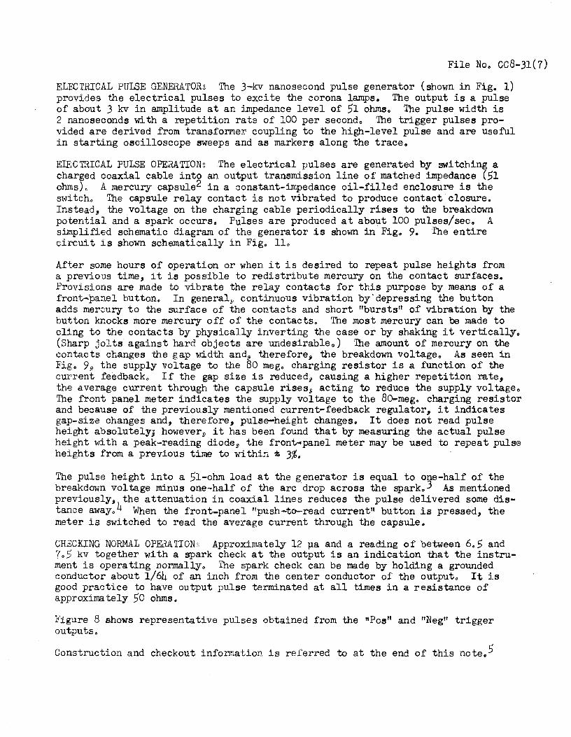
File No. cc8-31(7)
ELECTRICAL PULSE GEN&'i.ATORg The 3-kv nanosecond pulse generator (shown in Fig. 1) provides the electrical pulses to excite the corona lamps. The output is a pulse of about 3 kv in amplitude at an impedance level of 51 ohmso The pulse width is 2 nanoseconds with a :repetition rate of 100 per secondo The trigger pulses pro-vided are derived from transformer coupling to the high-level pulse and are useful in starting oscilloscope sweeps and as markers along the trace.
ELECTRICAL PULSE OPEH.ATION~ The electrical pulses are generated by switching a charged coaxial cable into an output transmission line of matched impedance (51 ohms)o A mercury capsule2 in a constant-impedance oil-filled enclosure is the switch. The capsule relay contact is not vibrated to produce contact closure. Instead, the voltage on the charging cable periodically rises to the breakdown potential and a spark occurs. Pulses are produced at about 100 pulses/sec. A simplified schematic diagram of the generator is shown in Fig. 9. 1be entire circuit is shown schematically in Fig. llo
After some hours of operation or when it is desired to repeat pulse heights from a previous time, it is possible to redistribute mercury on the contact surfaces. Provisions are made to vibrate the relay contacts for this purpose by means of a front-panel button. In general9 continuous vibration by'depressing the button adds mercury to the surface of the contacts and short "bursts" of vibration by the button knocks more mercury off of the contacts. The most mercury can be made to cling to the contacts by physically inverting the case or by shaking it verticallyo (Sharp jolts against hard objects are undesirablea) 1he amount of mercury on the contacts changes the gap width and9 therefore, the breakdown voltage. As seen in Figo 99 the supply voltage to the 80 meg. charging resistor is a function of the current feedback. If the gap size is reduced9 causing a higher repetition rate, the average current through the capsule rises9 acting to reduce the supply voltageo The front panel meter indicates the supply voltage to the 80-meg. charging resistor and because of the previously mentioned current~feedback regulator, it indicates gap-size changes and, therefore, pulse-height changes. It does not read pulse height absolutely; however, it has been found that by measuring the actual pulse height with a peak-reading diode 9 the front-.panel meter may be used to repeat pulse heights from a previous time to within z 3%.
The pulse height into a 51-ohm load at the generator is equal to one-half of the breakdown voltage minus one-half of the arc drop across the spark.3 As mentioned previously, 4the attenuation in coaxial lines reduces the pulse delivered some dis-tance awayo When the front-panel npush-to-read current" button is pressed, the meter is switched to read the average current through the capsule.
CHECKING NORMAL OPERATIONg Approximately 12 µa and a reading of between 6.5 and 7.5 kv together with a spark check at the output is an indication that the instru-ment is operating normally. The spark check can be made by holding a grounded conductor about 1/64 of an inch from the center conductor of the output. It is good practice to have output pulse terminated at all times in a resistance of approximately 50 ohms.
Figure 8 shows representative pulses obtained from the 11Pos" and "Neg" trigger outputs.
Construction and checkout information is referred to at the end of this note.'
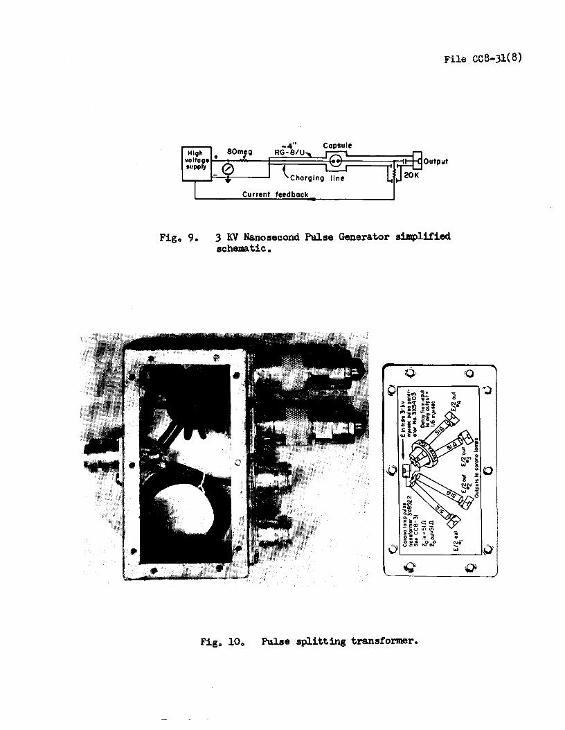
File ccS-31(8)
Capsule
Current feedback
3 KV Nanosecond Pulse Generator simplified schematico
O·
N
-~· !?CD ~x .. ..,_ a. "' e~· c:c: ..!:! ECD - -'-UL(') II) ~J?U II M
~:., .s ~ 0 0., 0 0
0, Ul:Ul l'\.I l'\.I
Pulse splitting transformer.
IQ
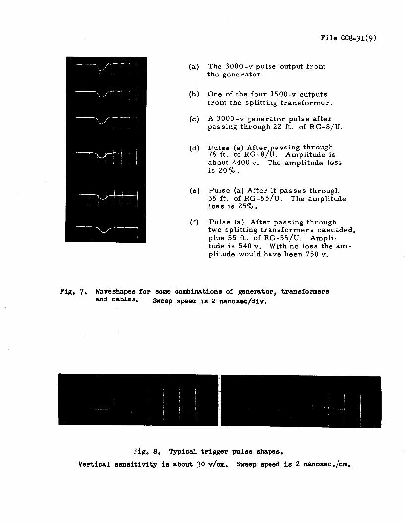
{a)
(b)
(c)
(d)
(e)
(f)
File CCS-31(9)
The 3000-v pulse output from the generator.
One of the four 1500-v outputs from the splitting transformer.
A 3000 -v generator pulse after passing through 22 ft. of RG-8/U.
Pulse (a) After passing through 76 ft. of RG-8/U. Amplitude is about 2400 v. The amplitude loss is 20 % .
Pulse (a) After it passes through 55 ft. of RG-55 /U. The amplitude loss is 25%.
Pulse (a) After passing through two splitting transformers cascaded, plus 55 ft. of RG-55/U. Ampli-tude is 540 v. With no loss the am -plitude would have been 750 v.
Fig. 7. Wavesha.pes for some combinations of generator, transformers and cableso SWeep speed is 2 nanosec/div.
Figo 80 Typical trigger pulse shapeso
Vertical sensitivit1 is about 30 v/cm. Sweep speed is 2 nanosec./cm.
File Noo CC8=31(10)
SPLITTING TRANSFORMERSg The input and output impedance of the splitting transformer is 51 ohmso Four equal and synchronous outputs are provided at just half the input voltageo Thus, one transformer can feed four others to produce sixteen identical signals at 1/4 the voltage level of the primary pulse generatoro The rise time of the transformers is adequate for an additional cascade9 from which there would be 64 output channels at 1/8 the voltageo There is some loss in rise time and amp= litude in the transformers 9 but it is less than the loss in cables that are used to delay and distribute the pulseso The transformers are constructed of four equal lengths (lo6 nsec) of miniature 51-ohm coaxial cable (RG174/U)o The series-parallel connection of the four cables may be seen in the photograph of the transformerj Figo 10. Two of the four cables have a voltage pulse along the shield length9 and are wound on a ferroxcube 102 toroid 1 ino in diameter to raise the impedance of this shunt patho
Figure 7 shows wave shapes for some combinations of generators9 transformers» and cableso RG9/U has been used for moderate delay9 RG55/U for short delays or patch cableso Styroflex cable 1-in diameter has been used for 150·nsec delay and would be satisfactory for delay up to a microsecondo GR874 cable connectors can be used with both RG/U cable typeso Type N connectors can be used with RG9/U and BNC connectors with RG55/Uo The generator, transformers9 and cabling systems have been maintained in coaxial configuration throughout in order to keep spurious radia-tion from other circuitryo (RG9/U and RG55/U are the double shielded versions of RG8/U and RG58/Uo)
REFERENCESg
lo Qo Ao Kerns and Go C. Cox, UCRL 92699 A Triggered Nanosecond Light Source» October 109 19600
2o The capsules used were obtained from the Western Electric 275C and from Co Po Clare and Company HG 1003 mercury-wetted contact relayso
3o Lewis and Wells.11 Millimicrosecond Pulse Techniques9 McGraw-Hill Co. 9 1954» Page 1000
4. Counting Handbook9 File Noo CC2-l.
5o 3-kv Nanosecond Pulse Generator 3X5403 and 3X5413. Engineering Note-~Assembly Details EET-747 Engineering Note--Checkout Procedure EET-770
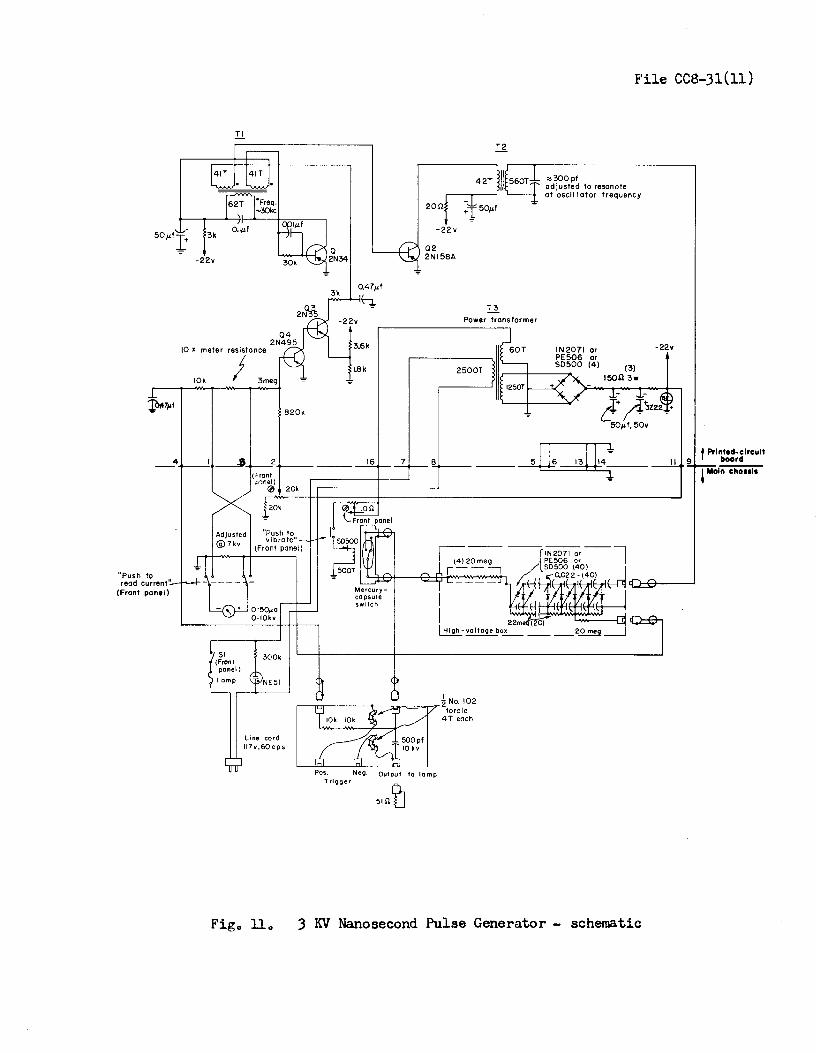
__ 4
1'Push to read current"
(Front panel)
File CCS-31(11)
10 x
.!.!
04 2N495
meter resistance
3k
I.Bk
20.n
-22v
02 2Nl58A
:::300pf adjusted to resonate at oscil later frequency
T3 Power trans former
2500T I Ok ! 3meg
I~ 2 (Front p'1nel)
820k
16 7 8 ~,._ __ ----~ 0 20k ~~---t-t------,----,---t---------------------------_J
Adjusted @7kv
"Push to vibrate"
(Front panel)
Line cord lt7v,60cps
Neg. Output fa lamp Trigger
3 KV Nanosecond Pulse Generator - schema.tic
f Prln~::;:lrcult ~ Main cha11l1
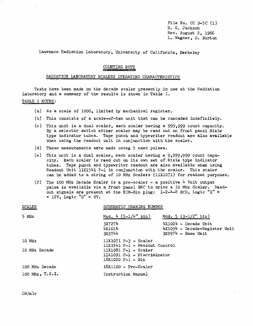
File No. CC 9-5C (1) H. G. Jackson Rev. August 2, 1966 L. Wagner, D. Burton
Lawrence Radiation Laboratory, University of California, Berkeley
COUNTING NOTE
RADIATION LABORATORY SCALERS OPERATING CHARACTERISTICS
Tests have been made on the decade scaler presently in use at the Radiation Laboratory and a summary of the results is shown in Table I. TABLE I NOTES:
(a) As a scale of 1000, limited by mechanical register. (b) This consists of a scale-of-ten unit that can be cascaded indefinitely. (c) This unit is a dual scaler, each scaler having a 999,999 count capacity.
By a selector switch either scaler may be read out on front panel Nixie type indicator tubes. Tape punch and typewriter readout are also available when using the readout unit in conjunction with the scaler.
(d) These measurements were made using 5 nsec pulses. (e) This unit is a dual scaler, each scaler having a 9,999,999 count capa-
city. Each scaler is read out on its own set of Nixie type indicator tubes. Tape punch and typewriter readout are also available when using Readout Unit 11Xl541 P-1 in conjunction with the scaler. This scaler can be added to a string of 10 MHz Scalers (11Xl071) for readout purposes.
( f) The 100 MHz Decade Scaler j s a pre-scaler - a positive 4 Volt output pulse is available via a front panel BNC to drive a 10 MHz Scaler. Read-out signals are present at the NIM-Bin plug: 1-2-4-8 BCD, Logic 111 11 = + 12V, Logic 11 011 = ov.
SCALER SCHEMATIC DRAWING NUMBER
5 MHz
10 MHz
10 MHz Decade
100 MHz Decade loo MHz, T.s.r.
LW/mlr
Mod. 4 (5-1/4" bin) 3x7274 4Xl014 3X3744 11Xl071 P-3 - Scaler 11Xl541 P-1 - Readout 11Xl081 P-1 - Scaler
Mod. 5 (3-1/2" bin) 4Xl024 - Decade Unit 4Xl034 - Decade-Register Unit 3X9974 - Base Unit
Control
11Xl091 P-1 - Discriminator 18Xl020 P-1 - Bin 18Xll00 - Pre-Scaler Instruction Manual
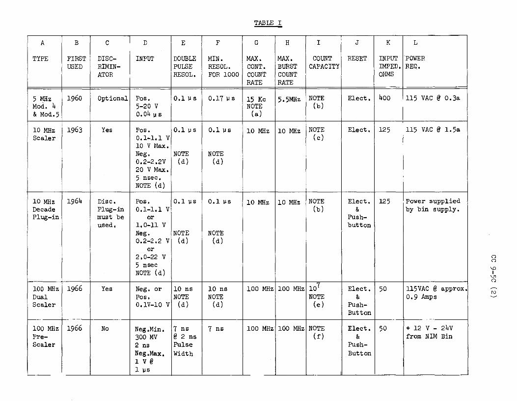
A B c D E F
TYPE FIRST DISC- INPUT DOUBLE MIN. USED RIMIN- PULSE RESOL.
ATOR RESOL. FOR 1000
5 MHz 1960 Optional Pos. 0.1 µ s o.17µs Mod. 4 5-20 v & Mod.5 o.o4 µ s
10 MHz 1963 Yes Pos. 0.1 µ s 0.1 µ s Scaler 0.1-1.1 v
10 V Max. Neg. NOTE NOTE 0.2-2 .2v (d) (d) 20 V Max. 5 nsec. NOTE (d)
10 MHz 1964 Disc. Pos. 0.1 µs 0.1 l.IS Decade Plug-in 0.1-1.1 v Plug-in must be or
used. 1.0-11 v Neg. NOTE NOTE 0.2-2 .2 v (d) (d)
or 2.0-22 v 5 nsec NOTE (d)
100 MHz 1966 Yes Neg. or 10 ns 10 ns Dual Pos. NOTE NOTE Scaler O. lV-10 v (d) (d)
100 MHz 1966 No Neg.Min. 7 ns 7 ns Pre- 300 MV @ 2 ns Scaler 2 ns Pulse
Neg.Max. Width 1 v@ 1 µs
TABLE I
G H I
MAX. MAX. COUNT CONT. BURST CAPACITY COUNT COUNT RATE RATE
15 Kc 5.5MHz NOTE NOTE (b)
(a)
10 MHz 10 MHz NOTE (c)
10 MHz 10 MHz NOTE (b)
100 MHz 100 MHz 107 NOTE
(e)
100 MHz 100 MHz NOTE (f)
I
J K
RESET INPUT IMPED. OHMS
Elect. 400
Elect. 125
Elect. 125 &
Push-button
Elect. 50 &
Push-Button
Elect. 50 &
Push-Button
L
POWER REQ,.
115 VAC @ 0.3a
115 VAC @ 1. 5a
Power supplied by bin supply.
115VAC @ approx. 0.9 Amps
+ 12 V - 24V from NIM Bin
0 0
\0 I
\J1 0
[\)
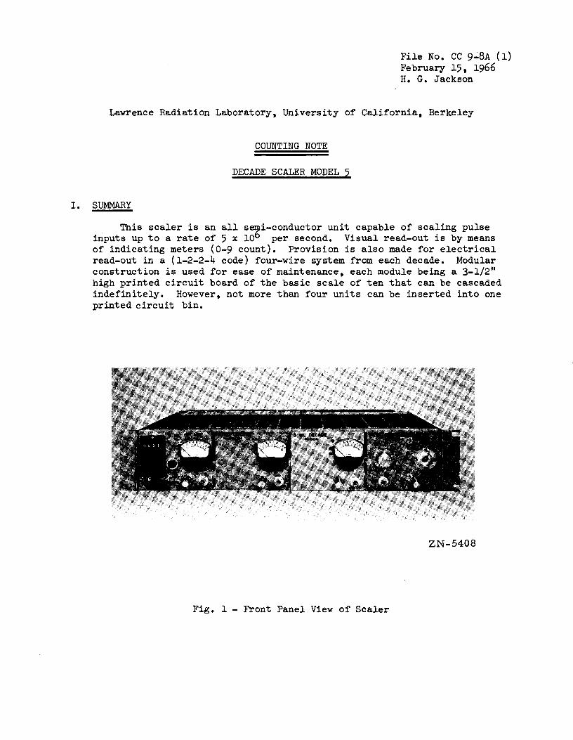
File No. CC 9-8A (1) February 15, 1966 H. G. Jackson
Lawrence Radiation Laboratory, University of California, Berkeley
COUNTING NOTE
DECADE SCALER MODEL 5
I. SUMMARY
This scaler is an all se~i-conductor unit capable of scaling pulse inputs up to a rate of 5 x 10 per second. Visual read-out is by means of indicating meters (0-9 count). Provision is also made for electrical read-out in a (1-2-2-4 code) four-wire system from each decade. Modular construction is used for ease of maintenance, each module being a 3-1/2" high printed circuit board of the basic scale of ten that can be cascaded indefinitely. However, not more than four units can be inserted into one printed circuit bin.
ZN-5408
Fig. 1 - Front Panel View of Scaler
CC 9-BA (2)
II. SPECIFICATIONS
Minimum resolution time Maximum counting rate Register speed
0.2 µs6 5 x 10 per second 15 per second (4-digit register)
Input Requirements
a)
b)
c)
Minimum amplitude - +5 V peak for pulses with rise time less than 20 ns. For pulses with rise times greater than 20 ns the required sensitivity is approximately 150 volts per micro second of rise time.
* Maximum amplitude - Approximately 4 times minimum amplitude of a).
Minimum pulse width - 0.04 µs.
Count Switch
a) In STOP position scaler does not count. b) In COUNT position scaler will count continually. c) In GATE position scaler will count only during the interval that
a +4 - +20V gate pulse is applied to the gate input.
Reset to Zero
Electrical and register reset obtained simultaneously by pushing reset button. Provision is also made for resetting remotely through an external reset connector on the rear chassis. This also allows for any number of units to be reset by one reset button.
Presentation - Visual by.means of indicating meters (0-9 counts).
Readout
By means of a 4-wire system from each decade (1-2-2-4 code). Open circuit voltage is -7 volts for "O" state and -13 volts for "l" state with an internal impedance of 10 kilohms.
* Memory time of the first flip-flop is about 200 ns. Input pulses of 200 ns width with the trailing edge of the pulse falling faster than 150 volts per micro second may cause double counting. This problem does not occur for input pulses with widths appreciably shorter or longer than 200 ns.

cc 9-BA (3)
Input Impedance - Scaler input 400 ohms; Gate input 7.4 kohms.
Note It is recommended that in general the first decade be preceeded by the 10 MHz discriminator. (See Counting Note No. CC 3-11).
Power Requirement - 115 V AC at 0.3 A.
A picture of the front panel is shown in Fig. 1. A block diagram of the unit as a scale of 1000 is shown in Fig. 2.
Gate 4
Ext. Reset
Decade Register Unit
4
Decade Unit
3
Decade Unit
2
Decade Unit
Fig. 2 - Block Diagram - As a Scale of 1000
Rear Chassis
Front Panel
Bin No.
MU B-9894
The modular construction allows for a selection of scaling units in the printed circuit bin:
a) Four decade units arranged as a scale of 10,000. b) Three decade units arranged as a scale of 1,000 with one spare
position available. c) Four decade units arranged as two scales of 100. d) Two decade units arranged as two scales of 10 with two spare
positions available. e) Four decade units arranged as four scales of 10.
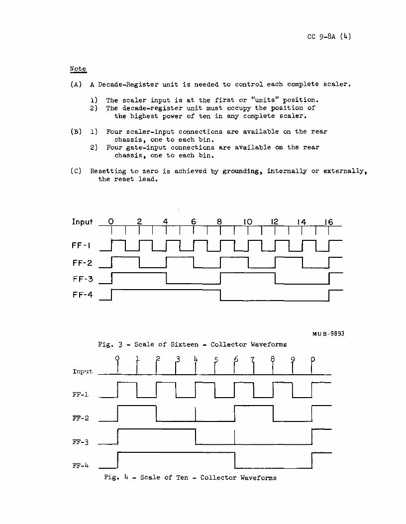
CC 9-8A (4)
Note -(A) A Decade-Register unit is needed to control each complete scaler.
1) The scaler input is at the first or "units" position. 2) _The decade-register unit must occupy the position of
the highest power of ten in any complete scaler.
(B) 1) Four scaler-input connections are available on the rear chassis, one to each bin.
2) Four gate-input connections are available on the rear chassis, one to each bin.
(C) Resetting to zero is achieved by grounding, internally or externally, the reset lead.
Input
FF-I
FF-2
FF-3
FF-4
Inp'.lt
FF-.1
FF-2
FF-3
FF-4
0 2 4 6 8 10 12 I I I I I I I
_J _J _J
Fig. 3 - Scale of Sixteen - Collector Waveforms
0
' _J _J _J
t L t i
Fig. 4 - Scale of Ten - Collector Waveforms
14 16 I I
MUB-9893
r r
CC 9-BA (5)
III. CIRCUIT DESCRIPTION
1. 5-MHz Decade Unit (4Xl024) The collector waveforms of a scale of sixteen are shown in Fig. 3. These are the waveforms of a scaler without feedback using four flip-flops connected in the usual binary fashion. The waveforms show that sixteen input pulses are required to obtain a complete cycle in which all the collector-waveform voltages are returned to the initial state. A scale of sixteen may be converted into a scale of ten by using feedback and then it requires only ten input pulses to obtain a complete cycle in which all the collector-waveform voltages are reverted to their initial state.
Figs. 4 and 5 show the collector waveforms and the block diagram for a scale of ten, respectively.
Input I ---.. 9'4: FF - I I .. 1 FF - 2 .____...I FF - 3 I ·I FF - 4
...__.,........ .. I I .. I
Fig. 5 - Scale of Ten - Block Diagram
I Outpu!
MUB-9895
In this unit the scale of sixteen is reduced by a count of six to a decade scale, through a feedback network, in two operations. Fig. 5 shows the block diagram of the decade scale and indicates the feedback. Referring to Fig. 4, with the fourth pulse FF-2 is reset by a pulse from FF-3 and the count is reduced by a count of 2. Then with the sixth pulse FF-3 is reset by a pulse from FF-4, and the count is further reduced by a count of 4. It may be noted that FF-2 must be reset on the fourth pulse but remain undisturbed ·on the sixth. On the sixth pulse FF-3 is reset before it is completely set, then after differentiation the unwanted pulse is about one-third the amplitude of the wanted pulse. A biased diode is used in the feedback network to discriminate against this small signal.
The visual readout is achieved by means of a meter which reads the sum of four currents, one from each flip-flop. The deflection of the meter is proportional to the residual count in the decade.
CC 9-8A (6)
The electrical readout is by means of a 4-wire system (1-2-2-4 code). Each of the four flip-flop outputs from each decade is connected through a 10 kilohm resistor and brought out to a connector labeled "Scaler Pr int-Out • 11
A small hole in the front panel, in approximately the middle of the panel, allows access to a small trimming potentiometer located on the printed circuit board of each decade unit. With no power applied to the scaler, the pointer on the meter should indicate zero. If not, adjust the mechanical zero-adjust screw on thP meter. On the ninth pulse, the pointer should indicate nine. If not, adjust the potentiometer.
2. Decade Register Unit (4Xl034) This unit is identical with the Decade Unit except for the addition of a) the register; b) the count switch and c) the reset button.
The input to each scaling unit takes the form of a diode AND circuit. With the count switch on STOP, one diode (CR-2) is conducting and signals at the scaler input will not trigger the unit. With the switch on COUNT, the diode is rendered non-conducting, and the signals will now trigger the unit. In the GATE position, this diode is normally conducting and is rendered non-conducting with the presence of a gate signal. A zero volt signal gates the scaler off; a +4 volt signal allows the scaler to count.
The reset push button energizes the register reset coil which resets the register to zero and opens two contacts which allows the flip-flops in the scaling units to reset to zero. Provision is also made for operating the register reset coil remotely through an external reset connector located on the rear chassis.
3. Base Unit (3X9974) This unit is a 3-1/2" high type printed circuit bin and contains the permanent wiring associated with the printed-circuit connectors, and also the power supply. The power supply is located on the hinged panel at the rear of the base unit. The power supply supplies 15 volts @ 450 ma, and each decade with registers draws 75 ma, and decade without registers draw 60 ma.
CC 9-8A (7)
ZN-5407 Fig. 6 - Rear Panel of Base Unit
Fig. 6 shows a picture of the rear panel of the base unit. The two "EXT. RESET" connectors are paralleled so that several scalers can be reset at the same time. The "PRINT" connector contains the connections to each decade for the ( 1-2-2-l+) code to a scaler print-out unit.
The "GATE" inputs are only connected to the decades with registers (only one gate input needed for each register unit in the bin).
The four other connectors labeled "SCALER" are the outputs of each decade.
Engineering Schematics
5-MHz Decade Scaler 5-MHz Decade Scaler with Reg. Base Unit
HGJ/mlr
4X1024 4Xl034 3x9974
JK
-1.rv
l7 K
.?.!'O !:: /K
' -;;1
.!'?.< ~o ; /K /K' ;7'so ,,
" /.tY.fffA
=l /K ~o /K
/N"N
"
! /:.-(J //Ji::>. A /IV 1#121 /N
~~---+--+--'-"'-+-"""~,,,,.~~'------>-----+---------+~''~"-+------------J
52 "6ATC
,.,,.., I . .Jthf/1>61l5 A/IE IND1f.,ATEP 1IY D z. C1t1~ 'Cll/6 ARE HOVNrED ON rN£ /lE61'5T1ili!. .!. lt!S2, C~/.C21 AttHOl.HffED ON THE All11LIA.f'Y 80Ai!D "' ALL llESIST1JllS AR£.Jf4wm EXCLPT AS Nt>T'ED
FF·/
1-;~; -;R-;;f/IT-; -;;lf'HI-;; ;;,ED- - -I LINE IS ON JI,/ AJ./XILIAIZY llCAflD I
I I I L _____ _
·I.FY
,. K
Fr-.J
2NIH3
~·------------------------
/Ok F,C--f/l
- I I
I I I I
~N'//tlJ 1.::,0,,..~ fV' -1.f'"£1__ I ,,
~.r I K
~ ~ >---
1 0, I
: ;/ ""-1.::>0~
~' r7 rh IN"?&
I I
- -- - - _I
Fig. 7 - Decade Scaler Model 5 Schematic
I
-/#38
>---
f_, _, I
_, -/.r-
o/r
I
~tr.JET
1,
£7elf~P ~Jep ~142! 6'Ml!D Ourl.l#tl~ 4.f 1105- 2C
-t=~ 6NP. e;.,,,re
" ,. -/5V
Li: -JSV .
/ ovr . , ' ,,,
c " - _,, " _,. . .
A"Esrr ,t:"'_,e--'fl , ,.,..._,
' r.r-c ' ' _, ovr
F!ZHE'D ./IOA!i!O ~Ul'f~I
MAIUJ OVTLll(E" 4%4/H-/
0 n \0 I g' co

File No. CC 9-9 (1) January 13, 1964 H. G. Jackson
Lawrence Radiation Laboratory, University of California, Berkeley
COUNTING NOTE
REGISTER UNIT - 11X2411 P-1
I. SUMMARY A 4-digit register is operated by a +4 V logic level applied to a
monostable multivibrator. The register is reset manually or by appli-cation of a standard +4 V logic level1 to another monostable multi-vibrator. A pair of relay contacts (normally closed) are operated by the reset coil. Connection to these contacts is by the rear connector.
The unit is packaged in a shielded nanobox. A size 4X box (3 x 5-1/4") is used.
REGISTER
• •
•• UX24IO Pl
Fig. 1 - Register Unit -- Front View II. SPECIFICATIONS
Input (Count and Re set) Impedance 1 K Q
111 11 Level +4 V 110 11 Level -1 V
Min. trigger width 100 ns Max. count rate 24 pps Relay Contacts pins 16 - 17
Power Required +24 V 320 mA pin 12. +12 V 40 mA pin 10. -12 V 4 mA pin 21. Ground pin l.
1 See CC 5-9 for logic voltage levels.
HGJ:mt
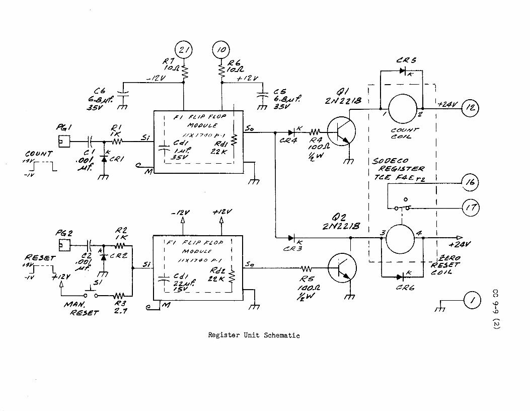
R.3 Z.1
.Si
r12Y
-12V +IZV
I Fl Ft. l.P FL OP I MOCVLE
I /IX/7st0 P-1 .So
Register Unit Schematic
~/ 2/'1221.8
~2 2/'122.1.S
I
IStJPG~o l RGG-l.S76R T~E /:4£ rz.
I 0
4
+24// _ !.ceA?o l'<G.$€7'"
k t! I!) ,I/.
0 0 .,J;) I
.,J;) -I\)
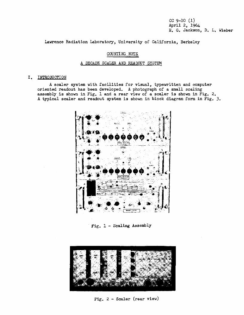
cc 9-10 (1) April 2, 1964 H. G. Jackson, D. L. Wieber
Lawrence Radiation Laboratory, University of California, Berkeley
COUNTING NOTE
A DECADE SCALER AND READOUT SYSTEM
I. INTROWCTION A scaler system with facilities for visual, typewritten and computer
oriented readout has been developed. A photograph of a small scaling assembly is shown in Fig. 1 and a rear view of a scaler is shown in Fig. 2. A typical scaler and readout system is shown in block diagram form in Fig. 3.
Fig. 1 - Scaling Assembly
Fig. 2 - Scaler (rear view)

EX T GATE- STATION GATE -·~ I , 1 ENABLE
PRINT COMMAND ART ·-ST
R/ FIRST TRANSFFR SECOND lRA~ ADVANCE 0 RESET - STATION CONTROL
CONSOLE DISPLAY SELECT ONE -8-LINE CODE - 1
j f & STOP R/0 TRANSFER FROM FINAL STATION
I I
PAPER TAPE TYPEWRITER PUNCH
cc 9-10 (2)
- -
,
STATION TWO
- I - ----------
Fig. 3 - Scaler and Readout System Block Diagram
Each scaler chassis contains two six-decade scalers capable of count-ing pulse inputs up to a rate of 107 per second. Visual readout is provided by six Nixie tubes, so that contents of either-scaler may be visually dis-played. Each scaler has its own discriminator with a front panel sensitivity control.
The readout control console accepts binary coded decimal (BCD) infor-mation from the scalers in serial form, processes the data and records it on a typewriter and/or a paper-punch. The Control provides for remote gating, reset, and selection of display mode. It can operate on an unlimited number of scalers, since all control signals are regenerated in each scaler chassis. The control cables are connected in series between scalers. The BCD infor-mation from the decades is fed to the Control Console on 4 wires. An addit-ional 4 wires are provided so that parity check, end of line, and alphabet codes can also be transmitted.
II. DUAL SCALER (11Xl071 P-3) A block diagram of the Dual Scaler is shown in Fig. 4. The twelve decade cards have a common reset line. Both manual and
automatic reset facilities are available. In the automatic mode, a switch allows the stored count to be either erased or retained after a Count-Readout cycle. Another switch provides for the carry output from any decade to be applied to the Decade Out connector. A light indicating that a carry output has been made.
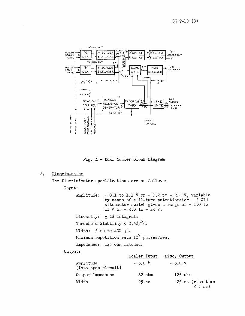
POS. IN NEG. IN
GATE
POS. IN NEG. IN
GATE
0 u Ill
"' z :;; "'
"A" DISC. OUT
I _L RESET STORE RESET
~
"' .... <( l!)
a: ":l <( u "'
.... 0"' z ... ~ r2 ~ ~ w
ffi ~ ~ ~ ;;! ~ ~ Ei iii Q. ... <(
READOUT SEQUENCE
B-LINE BCD
NOTE: W= WIRE
Fig. 4 - Dual Scaler Block Diagram
cc 9-10 (3)
TOIO CATHODES
T06
A. Discriminator The Discriminator specifications are as follows:
Input: Amplitude: + 0.1 to 1.1 V or - 0.2 to - 2.2 V, variable
by means of a 10-turn potentiometer. A XlO attenuator switch gives a range of + 1.0 to 11 V or - ~.o to - ~~ v.
Linearity: ± 1% integral. Threshold Stability < 0.5%;°c. Width: 5 ns to 200 µs.
7 Maximum repetition rate 10 pulses/sec. Impedance: 125 ohm matched.
Output:
Amplitude (Into open circuit) Output Impedance Width
Scaler Input + 5.0 v
82 ohm 25 ns
Disc. Output + 5.0 v
125 ohm 25 ns (rise time
< 5 ns)
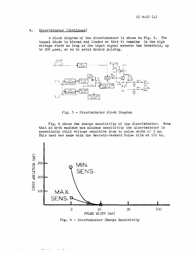
cc 9-10 (4)
A. Discriminator (Continued)
A block diagram of the discriminator is shown in tunnel diode is biased and loaded so that it remains voltage state as long as the input signal exceeds the to 200 µsec, so as to avoid double pulsing.
4 TO IOV _J--1_ GATE INPUT ___ .,
-12v
pF
l._ _ _f
Fig. 5 - Discriminator Block Diagram
Fig. 5. The in the high threshold, up
Fig. 6 shows the charge sensitivity of the discriminator. Note that at both maximum and minimum sensitivity the discriminator is essentially still voltage sensitive down to pulse width of 5 ns. This test was made with the Hewlett-Packard Pulse 215A at 100 kc.
~ JOO
~ H ,_::i
~ 200 E-;
~ H 100 MAX.
SENS.
J
MIN. SENS.
10 PULSE WIDTH ( ns )
JO
Fig. 6 - Discriminator Charge Sensitivity
100
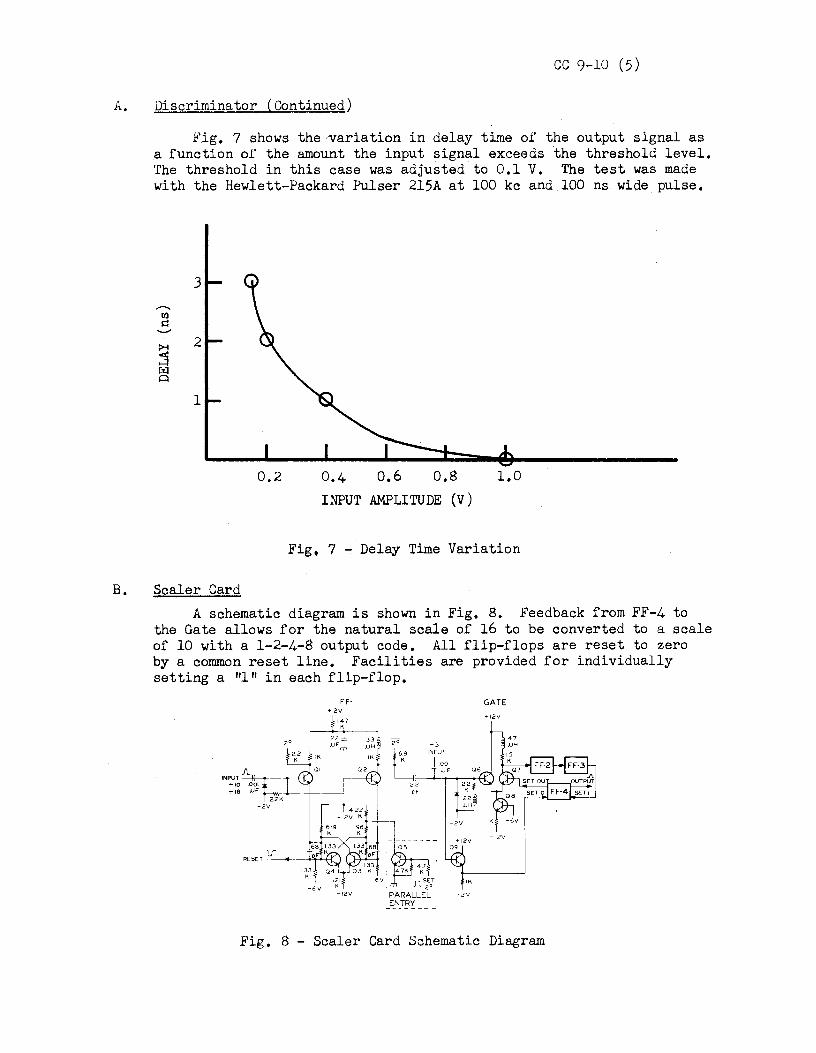
cc 9-10 (5)
A. Discriminator (Continued)
Fig. 7 shows the variation in delay time of the output signal as a function of the amount the input signal exceeds the threshold level. The threshold in this case was adjusted to 0.1 V. The test was made with the Hewlett-Packard Pulser 215A at 100 kc and 100 ns wide pulse.
3
2
1
0.2 0.4 o.6 o.8 1.0 INPUT AMPLITUDE (V)
Fig. 7 - Delay Time Variation
B. Scaler Card A schematic diagram is shown in Fig. 8. Feedback from FF-4 to
the Gate allows for the natural scale of 16 to be converted to a scale of 10 with a 1-2-4-8 output code. All flip-flops are reset to zero by a common reset line. Facilities are provided for individually setting a "l" in each flip-flop.
FF-I GATE +12V
I 47 + 12V
K
22 33 25 47 JJFJ; JJH
_, JJH
~ INPUT IK 1001
}\_ Q2
~ INPUT~ -:-10 .001 22 -:-16 JjF pF
-2V
1--------, + 12V -12V
I as 09 1.)
RESET
-6V I IK
-12V -2V
Fig. 8 - Scaler Card Schematic Diagram

cc 9-10 (6)
c. Display and Scan Circuits. Referring to Fig. 4; the Scan Gates are logical "AND" circuits
and allow for the 4-line BCD code from each decade to be presented, in turn, to the Nixie Decoder, and also to the Central Console. Twelve such gates are used, one for each decade.
The Nixie Decoder card decodes the 4-line BCD input to a 10-line decimal output. Connection is then made to the appropriate Nixie tube cathode. Selection of a particular Nixie tube is made by gating the anode through the Nixie Gate card. By the use of diodes in the 10-line output, both odd and even parity check bits are generated on this card.
D. Program Card The routing of the gate pulses/is done through a Program Card.
The program card is essentially a 30 x 30 matrix with diodes being used to route any of the JO output positions of a Sequence Generator to any of the JO program output lines.
Only 12 output positions are needed for decade readout, with two additional positions to identify the two scalers. This allows fixed information such as; day, run number, computer instructions, etc., to be loaded by means of diodes into the Program card in BCD code and appear on the print out along with the scaler stored count.
E. Sequence Generator and Station Control. The source of the gate pulses in the Sequence Generator card
which is a ring counter with JO positions. Except during remote read-out, the Sequence Generator is driven by a 2 kc clock to allow continuous visual display. The clock signals are generated by the Station Control card which also contains the logical control circuits used in the automatic print out of the scaler.
III. CONTROL CONSOLE (11Xl541 P-1)
As a part of the Decade Scaler and Readout System, the Control Console performs the following functions:
i) controls the scaler visual display. ii) controls the scaler data accumulation gates, provides for preset
count or preset time operation. iii) operates through the Station Control card of each scaler to generate
control logic and handle data for automatic scaler readout onto a Tally Series 420 Tape Perferator and/or an IBM Series 73 Selectric Typewriter.
A. Control Logic. A simplified Control Console block diagram is shown in Fig. 9. The
chronological sequence of events in a normal automatic read-out operation, in which both a papertape punch and a typewriter are recording is shown below.
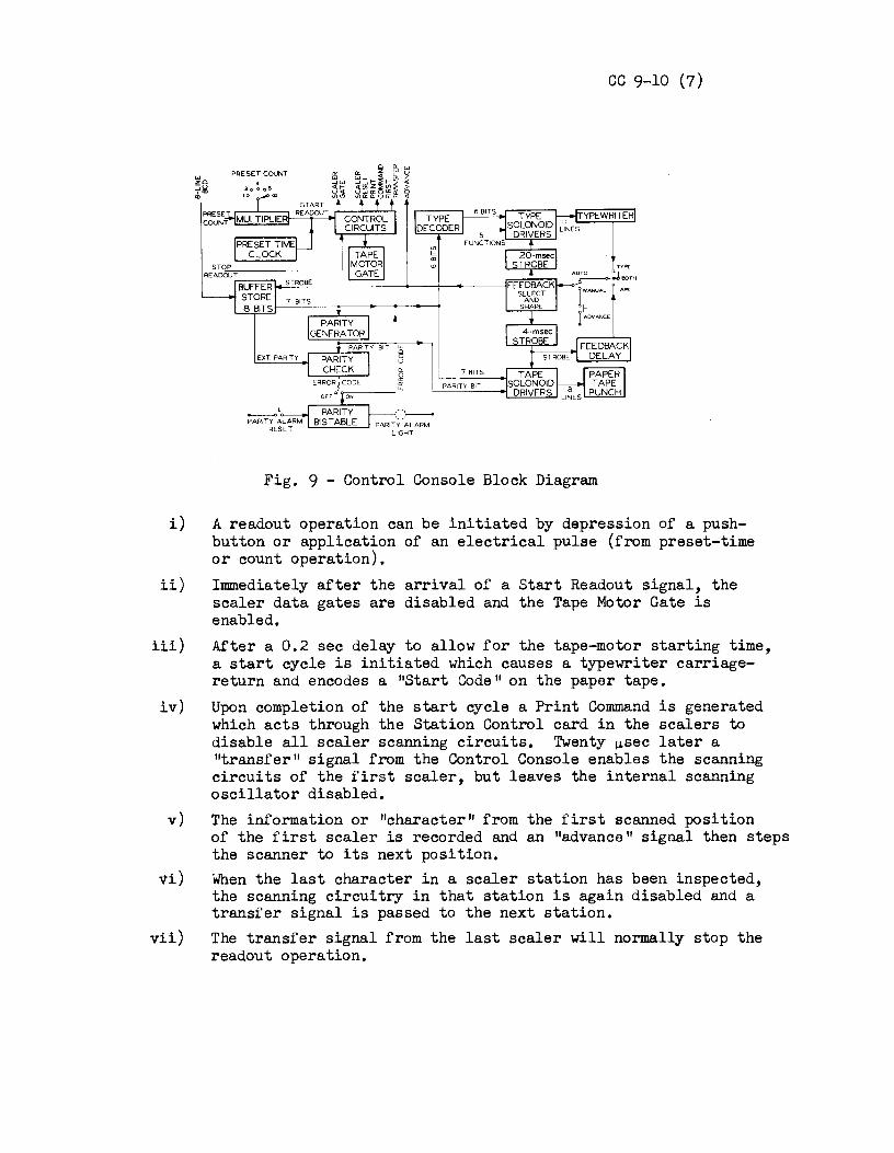
i)
ii)
iii)
iv)
PRESET COUNT . 2 0 o 08 ,.
EXT PARITY -~-P-AR-ITY BIT 8
u
~ "' .,..,_~-w
~-'- PARITY PARITY ALARM BISTABLE
RESET
TYPE DECODER
Fig. 9 - Control Console Block Diagram
cc 9-10 (7)
A readout operation can be initiated by depression of a push-button or application of an electrical pulse {from preset-time or count operation). Immediately after the arrival of a Start Readout signal, the scaler data gates are disabled and the Tape Motor Gate is enabled. After a 0.2 sec delay to allow for the tape-motor starting time, a start cycle is initiated which causes a typewriter carriage-return and encodes a "Start Code" on the paper tape. Upon completion of the start cycle a Print Command is generated which acts through the Station Control card in the scalers to disable all scaler scanning circuits. Twenty µsec later a "transfer" signal from the Control Console enables the scanning circuits of the first scaler, but leaves the internal scanning oscillator disabled.
v) The information or "character" from the first scanned position
\ti)
vii)
of the first scaler is recorded and an "advance" signal then steps the scanner to its next position. When the last character in a scaler station has been inspected, the scanning circuitry in that station is again disabled and a transfer signal is passed to the next station. The transfer signal from the last scaler will normally stop the readout operation.
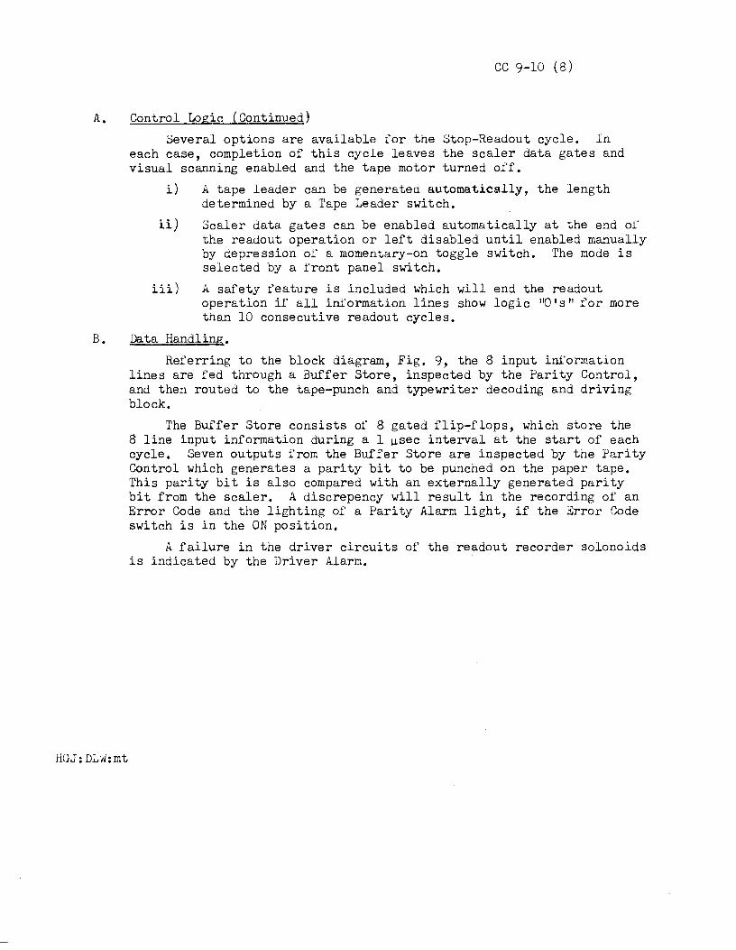
cc 9-10 (8)
A. Control Logic (Continued) Several options are available for the Stop-Readout cycle. In
each case, completion of this cycle leaves the scaler data gates and visual scanning enabled and the tape motor turned oi'f.
i) A tape leader can be generated automatically, the length determined by a Tape Leader switch.
ii) Scaler data gates can be enabled automatically at the end or the readout operation or left disabled until enabled manually by depression of a momentary-on toggle switch. The mode is selected by a front panel switch.
iii) A safety feature is included which will end the readout operation if all information lines show logic "O's" for more than 10 consecutive readout cycles.
B. Data Handling.
HGJ:DLw:mt
Referring to the block diagram, .Fig. 9, the 8 input information lines are fed through a Buffer Store, inspected by the Parity Control, and then routed to the tape-punch and typewriter decoding and driving block.
The Buffer Store consists of 8 gated flip-flops, which store the 8 line input information during a 1 µ.sec interval at the start of each cycle. Seven outputs from the Buffer Store are inspected by the Parity Control which generates a parity bit to be punched on the paper tape. This parity bit is also compared with an externally generated parity bit from the scaler. A discrepency will result in the recording of an Error Code and the lighting of a Parity Alarm light, if the Error Code switch is in the ON position.
A failure in the driver circuits of the readout recorder solenoids is indicated by the Driver Alarm.
Lawrence Radiation Laboratory, University of California, Eerkeley
COUNTING NOTE
GENERATORS OF FAST-RISING ELECTRICAL PULSES
File No. CCl0-1 Page l Jan. 10, 1959 G.C. Cox
ABSTRACT: Two UCRL mercury-capsule electrical-pulse generators are described which provide rectangular pulses with a 10 to 90~ rise time of less than 5 x lo·lO seconds at a repetition rate of 6o per second, one per second or single pulse.
The first generator Fig. 3, called the "mack Box Mercury Pulser", Dwg. No. 4V 4333, has been in use at UCRL since 1955.1 It has been re-packaged, resulting in Model lX 6693, Fig. 2. This second version conveniently momits in the Tektronix 517 "scope" cart, and is available with an output impedance of 52 ohms or 125 ohms. These pulse generators aire usefUl in measurements of transient response in the lo-9 second re-gion.
CHARACTERISTICS CC>!MON TO BOTH GENERATORS: Rectangular pulses of either polarity with a rise time of less than 5 x lo-10 seconds are generated by closing the con-tacts of a mercury-capsule switch,2 connecting the center c2nductors of two coaxial transmission lines which are charged to different voltages.j One, called the charg-ing line, which has an impedance of 52 ohms, is usually a length of RG8/u. The center conductor of the charging line returns to a voltage source through a 51K ohm charging resistor. When the switch closes, a pfll.se is obtained across the tennin-ated output whose width is twice the transit time of the charging line. The pulse amplitude is one half the voltage that is across the switch prior to closing.
The generators have a charging voltage sU,PPly which is adjustable from zero to 200V, thus the pulse amplitude is adjustable from zero to lOOV. The pulse amplitude is correctly indicated by the dial setting if the output is tenninated. If the output lines are not terminated, the output pulse amplitude then does not agree with the dial setting.
The pulse width depends upon the length of cable connected to the "Charging Line" connector. The minimum pulse width obtainable is determined by the transit time of charging line included inte:rnally between the switch contacts and the "charging line" connector. This is 0.19 millimicroseconds :for the "BJ.ack Box Pulser" and 0.245 millimicrseconds for lX 6693. Thus the pul.se width is 2 (L + 0.19) millimi-croseconds and 2 (L + 0.245) mill1microseconds for the two pulsers respectiveky, where L is the transit time o:f the charging cable used, in millimicroseconds. For long pulses, 1. e., a microsecond or more,, the charging line voltage, which rises on an RC time constant equal to 51K X the charging line capacitance, may reach significantly less than the supply voltage. In this case, the actual pul.se height will be somewhat below that indicated on the dial. The difference depends on the "open time" of the mercury switch• ''Open times" :for the two types of pul.sers and :for the various rep. rates are given in Table I.
l. Val Fish, Jr. , A Coaxial Mercury Relay :for Fast Pulse Genera ti on, UCRL 3062, July 1955·
2 • C .p • Clare and Co. , Type RP- 548o (same as used in Clare Type HG 1003 relays) • 3· Lewis and Wells, Millimicrosecond Pulse Teclmiques, McGraw-Hill Co., 1954,
Page 100. 4. Comiting Note, File No. CC 5-6, Page 2.
CClO-l (2)
TABLE I
OPRN TIME3 - Length of time available for re-charging the charging line preceding each pulse.
60 Per Second
"Black Box Pulser 10 Milliseconds
Pulser lX 6693 5 Milliseconds
l Per Second
1.iO Milliseconds
2 Milliseconds
Sipgle Pulse
Open Until The Button is Pressed
2 Milliseconds
A trigger output is available which is isolated from the main coaxial path and is su.fficientJ.y energetic to trigger the sweep circuits of the Tektronix 517. See Fig. 4 and 5.
Fig. 6 shows the output of a mercury capsule pulse generator connected to the vertical plates of the 5XPll CRT. This CRT limits the rise time to about one millimicrosecond; also, the pulse has traveled through about 100 millimicrosecond s (65 ft.) of RG8/U, slowing the rise and causing the top of the pulse to slope5 which would otherwise be "flat-topped". This length is used to give the sweep cir-cuits of the 517 "scope", time to start the trace.
The generators operate in an upright position. If tilted sufficiently, the switch becomes bridged by the contained mercury.
MODEL lX 6693: The pulse generator Model lX 6693, Fig. l and 2, has four features not found in the "Black Box Mercury Pulse Generator".
(1) With the case removed as seen in Fig. 2, the instrument will mount in the Tektronix "Scope Mobile" which carries the 517 oscilloscope.
(2) The pulse amplitude control has been decaded to allow vernier control of the lower pulse heights.
(3) The capsule enclosure has been redesigned. Two enclosures are available, with 52 ohm or 125 ohm outputs, Fig. l and 2 respectively. Th~y are interchange-able. Fig. 2 shows the 125 ohm pulser with an extra capsule enclosure. There are two 125 ohm outputs. If only one output is needed the other should be terminated to absorb the pulse energy which goes down the unused coaxial path.
(4) The mercury capsule switch utilizes the "normally closed" set of contacts. Thus a cycle of operation starts with the contacts closed. The contacts open after current flows in the driving coil, during which time the charging line volt-age builds up. The contacts then close, producing the output pUlse. When the generator is used in "single pulse" operation the normally closed condition re-sults in a newly-generated mercury surface on the contacts just prior to closing, hence, a more repeatable output pulse, regardless of the time between pulses.
>· Counting Notey File No. CC2-l.
Fig. 1 Model lX6693 with 52 ohm output.
File No. CCl0-1 (3)
Fig. 2 Model lX6693 with 125 ohm output and an extra capsule enclosure
Fig. 3 "Black Box Mercury Pulser"
A- Charging cable connector
B- Output
C- Trigger output

Power supply
Dwg. no. 1X6693
52 ohm Charging cable
o----__,
Trigger output 52 ohm output
File '.'Jo. CCl0-1 (4.)
Fig. 4 52 ohm capsule enclosure for Model 1X6693,
Power supply
Dwg. no. 1X6693
52 ohm Charging cable
+o--' - I 0
~ 0-····-·
1 12 ;ohms
! ~ --=;11 _.__L-iJd, 125 ohm output
125 ohm output
Trigger output
Fig. 5 125 ohm capsule enclosure for Model 1X6693.
Sweep Speed
l"O musec./crn.
lO musec./cm.
20 musec./cmo
File No. CCl0-1 (5)
Length of RG8/U charging cable used.
6 inches
30 inches
27 feet
Fig. 6 Waveforms from a "Mercury Capsule Pulse Generator".
v-1 082
V-2 082 /
ADJUST R-4 FOR 200V !. 2V ACROSS R5 (APPROX. IK, 2W)
r--------------------------, • I II VOLTAGE SELECTOR /K I PULSE AMPLITUDE AT MAX S-2A
.---------=--.,_~ ~P_G<4: ... 5H-i-7...,2'11\w,__,....._....--11t--. VERN 1 E R s ET T 1 NG 11 ............ ..., s-2
5 XTAL-/ /N/58
K XTAL-2 /N/58
XTAL-3 INl58
K
+
+
470K 25 K /OW
I I I
251 + Ml D' " I WW POWER od
PG4, 5-6
NE5/ v
ADJUST NORMAL OPEN CONTACT OF RE- I FOR ONE BOUNCE
ADJUST ARMATURE SPRING TENSION OF RE-I FOR 20VOLTS
P. P.
VIEW ACROSS C-l
l, ',
'
/OOV /OV /.V 90K /% _, I llK
LAR/T II
/%
"OUTPUT PULSE-AMPLITUD
VERNIER"
O/V /OOK /%
IOO.f1. 1%
', I
PG 4,5-3 c
SIGMA 8000 39K LG-SIL PG4,5-I IW
18K 2W
3K IW
PG 4,5 -5
''-------------------'
PG-3
NOTE-/% RESISTORS ARE DEPOSITED GARF' RESISTORS
SHIELD /X6762
RELAY ASSEMBLY IX6743 (125.f1. TERM) IX6753 ( 52 .0 " )
__.TO PG-5 S-f B / '------------------i'r--t
I I "PULSE REPETITION RATE" AMPHENOL I I 80-MC2FI L-------------------------J INSERT
lozJ ..... ...... (1)
z 0 . () ()
MUB-268 '""'
Fig. 7. Pulse Generator IX6693. Power Supply Circuit Diagram.
0 I ...... -O"
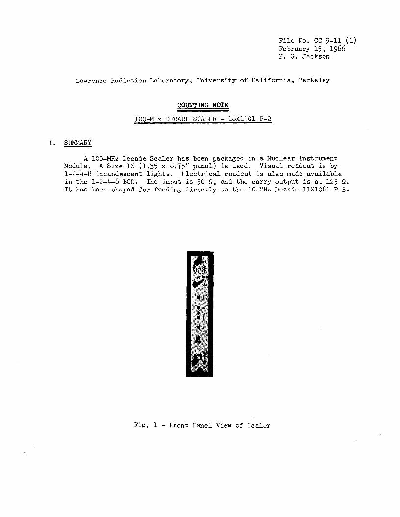
File No. CC 9-11 (1) February 15, 1966 H. G. Jackson
Lawrence Radiation Laboratory, University of California, Berkeley
COUNTING NOTE
100-MHz DECADE SCALER - 18Xll01 P-2
I. SUMMARY
A 100-MHz Decade Scaler has been packaged in a Nuclear Instrument Module. A Size lX (1.35 x 8.75" panel) is used. Visual readout is by 1-2-4-8 incandescent lights. Electrical readout is also made available in the 1-2-4-8 BCD. The input is 50 n, and the carry output is at 125 n. It has been shaped for feeding directly to the 10-MHz Decade 11Xl081 P-3.
Fig. 1 - Front Panel View of Scaler I
II. SPECIFICATIONS
Input Min • Amplitude Min. Width Impedance Max. Repetition Rate
Output Amplitude Width
Visual Readout Electrical Readout
Reset to Zero
Power Hequired +12 V 160 mA -24 v 160 mA Ground
III. CIRCUIT DESCRIPTION
pin 16. pin 29. pin 34.
cc 9-11 (2)
-200 mV (internally adjustable to -500 mV). 2 ns. 508~. 10 pulses/sec.
+3.5 V into 125 ~ (+7 into open circuit). 20 ns (risetime <10 ns). filamentary lamps (1-2-4-8). 1-2-4-8 BCD, at standard 4 V logic level. 1 "l" pin 20. "4" pin 22. "2" pin 21. "8" pin 23. manual by front panel push-button. electrical a) at standard 4 V logic level, 1
pin 35. b) by grounding line, pin 37.
A simplified schematic diagram is shown in Fig. 2. A simple de-coupled amplitude discriminator at the input allows for maximum sensitivity and still discriminates against noise. It also allows for pulse shaping independent of input pulse shape. Following the tunnel-diode discriminator the pulse is shaped, amplified and fed to the first binary.
2 The binary circuit follows the design of v. Radeka. A tunnel diode is used to switch the common-base transistors on and off. Steering diodes at the input obtain their bias from the transistor collectors. The fast-carry output from the binary is shaped and amplified before being fed to the second binary which is similar to the first. A slow output is also taken from each binary to drive the indicating light and the electrical readout lines.
The decade output is from a blocking-oscillator circuit triggered by the fourth binary.
~See CC 5-9 for logic voltage levels. V. Radeka. A Tunnel Diode and Common-Base Transistor Complementary Bistable., Nuclear Inst. Method g_ 123.
HGJ/mlr

IN
FDG114'1
LED 9!023 OR 21-1"70a,
FOG 114"'1 OR IN90+
LRL2021 OR htic!..2005
MA'\i?1
~ t;IA41Zl rso.n_ (>.81K. MF
i7.7.pH
12.K.
-7.4V
4.'1 K
i&.811<. MF
.001r.F
17 1
'2.K. SK. "2. z
~
-'2.4V
Fig. 2 - Schematic Scaler Diagram
MA41'Z.I
~1pF
'\I FOG 1147
-24-V,._. ____ _..._
'ZN 834
0 0
\0 I I-' I-'
w
Law~.:nce Radia-cion Labora.to:ry,, University of California.? Berkeley File No o CClO·~ 3 Page 1
COUNTING NOTE
NANOOECOND PULSE GENERATOR
December 24, 1958 Mo Nakamura
ABSTRACT: The Nanosecond Pulse Generator is an instrument designed primarily for testing counting equipment o Equi.pment requiring narrow input pulses of fast rise time at high repetition rates ma.y be tested with this generator, Three output channels (coincident in time) are availableo The output pulses are negative in polarity, 0 ~ 12 volts 9.mplitude with a rise timr:: of less than 2,5 nanoseconds, (10~9 seconds) and pulse widths adj".lstable from 2,5 to 2.5 nanosecondso The gen-erator output may be cont.rolled by single pulse operation, an external source, or by means of an internal generatoro The internal generator is capable of repe-tition rates of 10 cps to 10 Meo Provisions for gating the instrument allow bursts of pulses simulating operation with pulsed ace;elerators, Its high repe-tition rate capabilities make t.he instro.unen+. useful for checking equipment for such items as repetition rate sensitivity, base line shift, and pile up,
SPECIFICATIONS:
Repetition rate
Internal
External
Rise time~
10 cps to 10 Mc
lOcps to 10 Mc (sine -wave Input) 0 to 107 pulses per sec (pulse input)
less than 2o5 nanoseconds
O.itput pulse into terminated 125 ohm cable (3 channels independently adjustable for the following)~
Negative output pulse:
Pulse widths (by external clipping l.rne-s)
Trigger output;
Gate Input (gated operation)
External drive input:
Power requirements:
Weight:
0 to 12 volts
2, 5 1:,0 25 nanoseconds
20 volts positive, 50 nano-seconds wide
0 volt to close gate, +20 volt to open gateo
Positive pulse greater than 5 voltso Sine -wave input, see Fig. L
117 vol ts ac, approximately 200 -watts
Approximately 4o lbs,
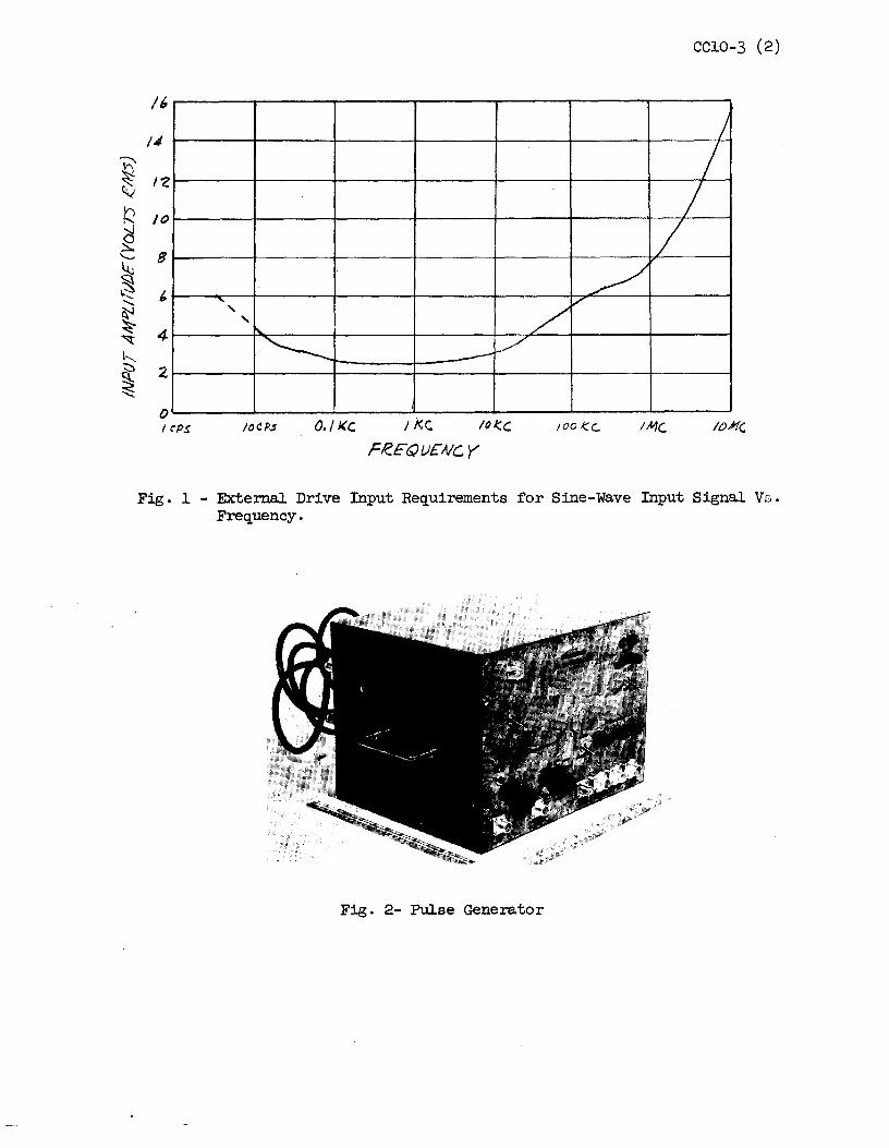
CCl0-3 (2)
16 /
I 1-1
7 I
/ ... v ' / ' "" '---- ---v
0 I ('PS /OCP~ ~/~c /KC Ntc ;ooJ::.c. I MC. IO#'!G
rR.FQ V£ lv'C Y
Fig. 1 - External Drive Input Requirements for Sine-Wave Input Signal vs. Frequency.
Fig. 2- Pul.se Generator
cc10~3 (3) OPERATING IR3TRUCTIONS~ The Nanosecond Pulse Generator is equipped with both an AC and a DC power switcho When the generator is not in immediate use, the ac power may be left on to maintain the filaments at operating temperature a See Figo 2o
The functions of the contr:ols and connectors is explained below:
Frequency~ The coarse frequency is selected by a 7 position switch on which the lower frequency limit is indicatedo The uncalibrated fine frequency control mul-tiplied by this lower frequency limit gives the approximate repetition rate of the internal generatoro The fine frequency control gives an over-lapping frequency control over the six decade positions on the coarse frequency range switch. When the coarse freg,uency control is in the "Ext./S ,p." position; the output pulse is controlled by either the Single Pulse push button or the External Drive Input Sig-naL
S!_l;gle Pulse: This push button allows single pulse operation when the coarse fre-quency range switch is in the "Ext .• /S , P. " position o
Externa.l Drive Input: When the coarse frequency range switch is in the "Ex.t./S.P. 0
positdonJ positive pulses of at least 5 volts amplitude will trigger the instrument at any repetition rate up to 10 Mc. If sine wave input is used for the external drive input s'ignal., the input amplitude required to trigger the instrument will vary as indicated in Figo l,
Positive Trigger Output: A positive 20 volt pulse, 50 nanoseconds wide precedes the ou.tput pulse by approximately 10 :nanoseconds for initiating timing or trigger-ing an oscilloscope,
Gate = Ungated Switch: In the "ungated" position.9 the gate allows all pulses (external» single pulse.~ and internal) througho In the "gated" position a pcsi-tive 20 volt signal at the '1Gate Input" connector is required to open the gate allowing pulses througho A gate signal of 0 volt will close the gateo
Gate Input: In the "gated" position a positive 20 volt signal will open the gate and all.owe-pulses througho A gate signal of 0 volt will close the gate. Because the :i.nput signal is direct=coupled" to the gate~ the lepgth of the gate signal may be any desired lengtho There is no provision within the instrument to synchronize th~ gate signal with the internal gener&tor. Turn-on and turn-off times of tlie gate are less than Q,l microsecond for a step f'Unction input. Fig. 3 shows some 10 Mc bursts of pulses obtainable when the gating feature is used in conjimction with the internal genera.tore
Outputs: Three ou.tputs are available based on the same source but independently variabl.e in pul.se ampl.itude and pul.se widtho The pul.se width is controlled by ex-ternal clipping at the rear of the instrumento· The output amplitudes are controlled at the front panel o The output pulse rise time is less than 2. 5 nanoseconds and pulse widths are adjustable from 2. 5 to 25 nanoseconds. The output pulse is vari-able from 0 to 12 volts negative when terminated into 125 ohm cable. Because of the use of clipping lines (or shorting stubs) to control the output pulse widths, there is no reverse tenninating resistor; therefore, it is mandatory that the load present a constant 125 ohm impedance to the genera.tor if spurious signals caused by .reflections are to be eliminated.
CCl0-3 l"i·) .
output Amplitide: These controls adjust the output arnplitude of each of the three output channels independently from 0 to 12 volts negative when terminated in 125 ohms. Fig. 4- shows the range of output amplitudes available.
Shorting Stubs (at rear of instrument): The output pulse widths of the three out-put channels are controlled independently by the insertion of the proper length of' shorting stub (or clipping line) in each of the three channels. The shorting stub must be 125 ohm cable, such as RG63/U. The output pulse width may be deter-mined by calculating the double transit t:illle for signals in the cable. The aver-age velocity of propagation in RG63/u is 9.9 inches per nanosecond. Fig. 5 shows the range in pulse widths available.
I -ml
I .. I -
l' • • • ' • • . (A) (B)
Fig. 3 - Bursts of 10 Mc pulses obtained when gating feature is used (vertical sensitivity = 16 v/c:m.; horizontal sweep = 0.25 usec/c:m.)
Fig. 4 output pulse amplitude varia-tions using multiple exposures. (Vertical sensitivity = 16 v/cm, horizontal sweep = 5 nsec/cm)
Fig. 5 - output pulse width var-iations using multiplie exposures. {vertical sen-sitivity = 16 v/cm; hori-zontal sweep = 5 nsec/cm)
CIRCUIT DESCRIPTION: A simplified block diagram of the instrument is shown in Fig. 6. The tubes associated with each function are indicated. The power su;pply in the instrument is omitted from the block diagram for s:implicity. The schematic cir-cuit diagram number 3X 2214 may be referred to for more detail.
The Single Pulse and External Drive Input signals_ trigger a Square Wave Generator (Vl, V2 and V3A) when the coarse frequency range switch is in the "E.xt./S.P.n position. In this switch position the Square Wave Generator is a monostable multi-vibrator whose pulse width and frequency are determined by the External Drive Input
CCl0-3 (5)
signal or Single Pulseo The External Drive Input may be either positive pulses or sine wave signalso The triggering level of the monostable multivibrator varies with sine wave input signal frequency. Fig. 1 shows the triggering level required as a function of the frequency of the sine wave input. Input pulse requirement is a positive pulse greater than 5 voltso
In the remaining six positions of the coarse frequency range switch, the Square Wave Generator is an astable multivibrator whose coarse frequency is determined by RC timing networkso The fine frequency adjustment returns the grid resistor to a variable potential that controls the frequency over a 10 to 1 range for axry selected coarse frequency range switch position.
The Gate (V3B) employs a cathode fol.lower coupling the differentiated signal from the Square Wave Generator to the first amplifier V4. When the Gate switch is in the 11 ungated" position, the cathode follower biases V 4 just beyond cut-off. In this 11ungated11 position the signals from the Square Wave Generator are sufficient to bring V 4 into conduction. When the Gate switch is in the "ga ted11 position~ V 4 is biased well beyond cut-off and signals from the Square Wave Generator are insuf-ficient to bring the grid of V4 into conduction. A positive 20 volt signal to the Gate {V.3B) is required to bring the grid of V4 to a bias level such that signals from the Square Wave Generator are sufficient to bring V4 into conduction.
The amplifiers V5 through V7 are each biased beyond cut-off and are driven into conduction by the signal. Signal inversion between amplifier stages is accomplished by pulse ·transformers. The signal drives each amplifier stage into conduction from cut-off, progressively steepening the rise time of the signal.
The llPositive Trigger Output" signal is taken from the grid of V5 and isolated f'rom the amplifier stages by Vl4 which is an output pulse amplifier with pulse transformer output.
Output amplifiers V9~ Vll9 and Vl3 are fed from the same source and driven into conduction from cut-off. The output amplitude of each amplifier is determined by its plate and screen voltages. Tubes V8$ VlO and Vl2 are cathode followers that control the plate and screen voltages o£V9, Vll, and Vl3, respectively. The po-tentials of the cathode follower are controlled by the potentiometer settings ad-justable at the front panel. These potentiometer controls are labelled "Amplitude" for the respective output channels.
The output pulse widths are determined by the length or 125 ohm cable inserted between PG-8 and -11;; PG-9 and -12~ and PG-10 and -13 for output channels 1, 2, and 3 respe~tively. If RG63/U is used for the shorting stub {or clipping line), the output pulse width will be equal to
P.w. = 21 I 9.9
where P.W. = the output pul~e width in nanoseconds,
L = the length of the shorting stub in inches measured from external ends of connectors 9
9.9 = the average velocity of signal propagation in RG63/U in inches per nanosecond.
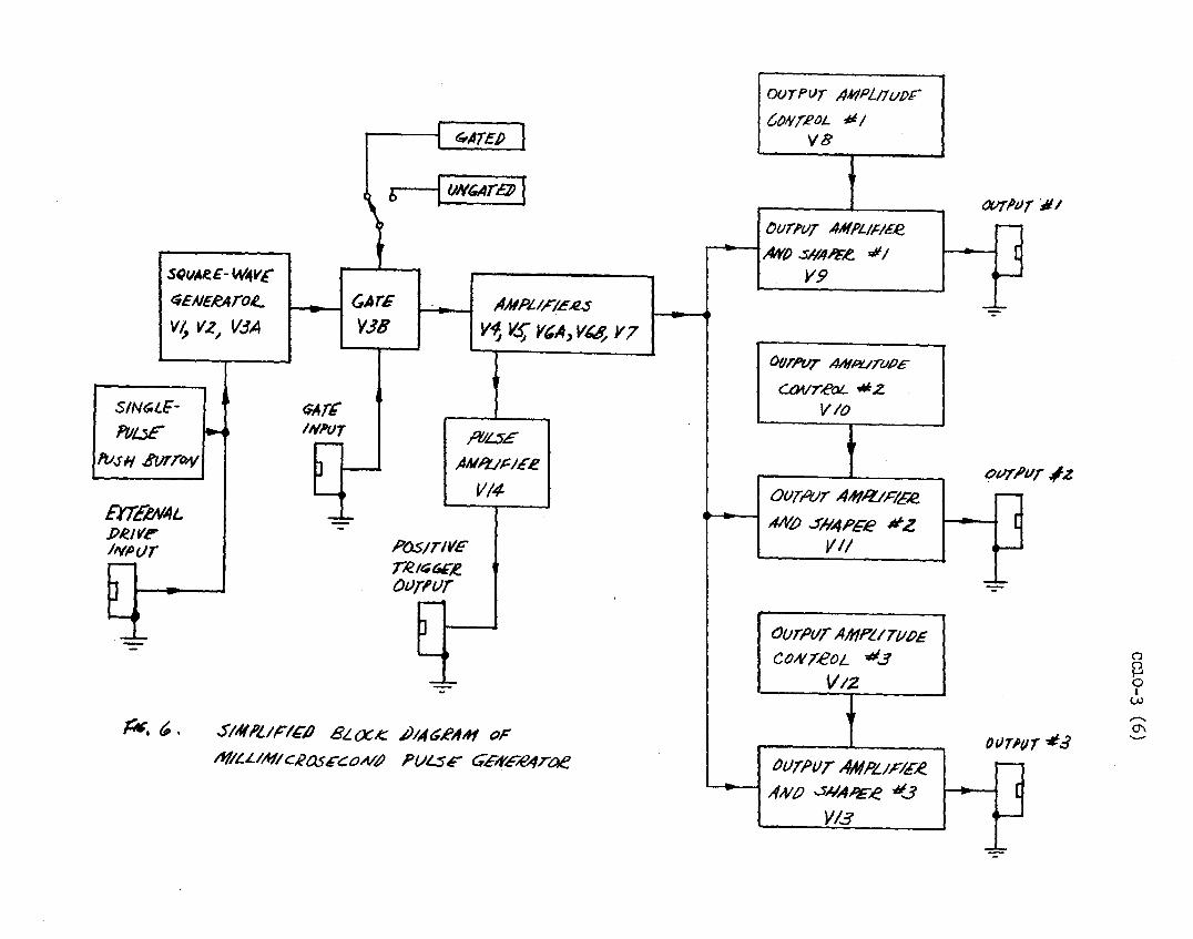
SQVA~£-fN.4Vl'
tiENE~TOl_
v~ v.z.1 V3A
S/Nt:.L~
Pf)LJE
-_,
---...1~ t;,ATEJ) I
' 6--[ IJN"ATO) ,,
.......... _~ GArG V.38
. - ANPL.l/"/EAZS
v~ ~ V,A, v~ Y7
-] ----
,Pl/L.SE ,4Alfl./~IEI!
POSITIVE rR.1t; 6«"K. 01)fftJT
0
V/4
S!Afl'LIFIG/) BLOCK ~IA6RA/lf OF 11!/LLIA11CRQ5ECOA//) !'VI.Sr GEIYER,it/rae
OUTPUT AMPL/TUPE'" tONTROL "'I
VB
I
OVrl'l/T AAIPL/!=1£12 MP S#A.PFe Ji I
V9
OurPV,- A/J/PUTVPE
c::ovreaL _. z. VIO
If
ovrmr 4.#!ll/FIER.. AN..O ..fllAPER "".Z
VII
OUTPtlT All/PL.I TllP£ COAITROL .-1.,s
V12 , t
OVTf>VT AAIPLJ,,&"IE-'!. ~--t AAltJ J#APEe *..3
V/3
-[
I.,__
-[
I..__
--
[ I~
---
(")
p 0 I w
CCl0-3 (7)
The output pulse must be terminated in 125 ohm cable if spurious signals caused by reflections in the output system are to be eliminated. These reflections could be serious where systems employ amplifiers and limiters in which the reflected signal may cause undesired operation.
SUMMARY: The Nanosecond Pulse Generator is an instrument designed primarily for testing counting eqµipment such as scalers, discriminators, coincidence units, and entire systems employing various pieces of counting equipment. The three-channel output of the instrument with variable repetition rate, ind~pendently adjustable output widths and amplitude, coupled with a gating feature make the instrument useful for simulating signals from experimental set-ups with pulsed accelerators. The narrow pulses with fast rise times simulate signals obtained from photomul-tiplier tubes. The specifications of the instrument will suggest many other uses for the instrument.
Inverting and coupling transformers described in CC2-4 may be used in conjunction with the generator to obtain positive pulses and to couple the signal from the gen-erator into systems employing other impedance levels.
BEFEBENCE: UCRL Drawing 3X 2214.

+ 150 GHIA
GATE~ INPUT 831R
IOOµ.µ.f
V> 6858
Fig. 7. Pulser Circuit Diagram.
File No. CC 10-3(8)
V7 7044
OUTPUT NO I
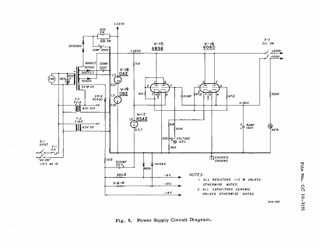
S-1 DPST F-I
2A
+225V
20K 2W
20K 2W
2XSD500 + -/OMF 450V
soov.c.r 125MF 350V V-18 + -
OA2
CR-9 T-2 SD500 F2/A
0 f 6.3V /OA X .__ _ ___J
2,4,7
T-3 F16X
--+----,,-6-.3-V_3_A_y
10!2 500MF 50 v
6BOJ2
51!2 /W
+220V
5/K
/OK
V-17 t,5 85A2
2,4,7
Nl591
V-15 6858
7
43
50K
IN/594
- 6 v.
-1211.
-14 v.
5/0K
0.IMF
V-16 6080
CHASSIS GROUND
47.{2
+150V
+ 40MF 150V
NOTES: I. ALL RESISTORS 1/2 W UNLESS
OTHERWISE NOTED.
2. ALL CAPACITORS CERAMIC UNLESS OTHERWISE NOTED.
Fig. 8. Power Supply Circuit Diagram.
S-2 D.C. ON
+220V .. +150V
300K
NE51
MUB-266
l%j ..... ...... CD
z 0 0
() () ...... 0 I l,J.) -'° -

Lawrence P.a.diation Laboratory, University of' California, Berkeley File No. CCl0-4 Page 1 March 15, 1961
COUNTING NOTE Designed by M. Nakamura
GATED PlJISE GENERATOR Note by T. Lawson
Fig. 1 - Gated Pulse Generator
AJETRACT: The Gated Pulse Generator is designed primarily f'or testing counting equipment. Its high repetition rate makes it usef'ul for checking equipment for such things as repetition-rate sensitivity, base-line shif't, and pile up. Internal or external gating provide bursts of' pulses simulating operation with pulsed ac-celerators. The instrument includes the following features:
(1) An output-pulse generator with a frequency range from 10 cps to 10 Mc. (2) A gate generator with a frequency range f'rom .1 to 100 cps. (3) Single pulsing of' either of these t"WO generators. ( 4) External drive of' the output-pulse genera tor. (5) A f'ast output, positive or negative, with a rise time of 25 to 50 ns. (6) A slow output, positive or negative, with a rise time of .6 µ.s. (7) A variable amplitude control f'or the f'ast and slow outputs. (8) Variable pulse-width control·s f'or the output pulse and for the gate pulse. (9) Internal or external gating of the output pulse. (10) Selection of' either on-gate or off-gate operation. (11) Internal gate output for gating other equipment. (12) Positive trigger output.
SPECIFICATIONS:
Output-pulse generator: Frequency: 10 cps to 10 Mc . Fast output:
Amplitude, no load, 1 Mc: 10 Mc:
± 16V, .5 µ.s wide. + 16V (17V peak-to-peak), 50 ns wide. - lOV (12V peak-to-peak), 50 ns wide.
125 ohm load, 1 Mc: + 8v, .5 µs wide. - 6v, .5 µs wide.
10 Mc: + 6v (8V peak-to-peak), 50 ns wide. - 4v (6v peak-to-peak), 50 ns wide.
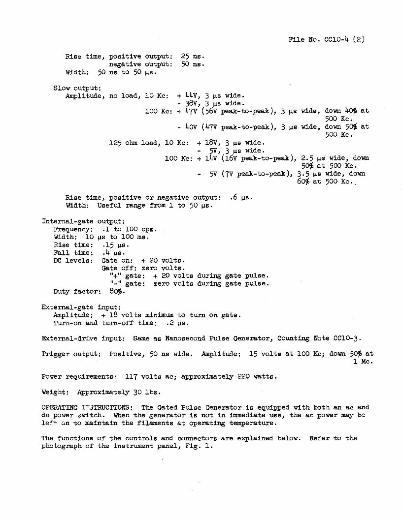
Rise time, positive output: negative output:
Width: 50 ns to 50 µs.
SJ.ow output:
25 ns. 50 ns.
File No. CCl0-4 (2)
Amplitude, no load, 10 Kc: + 44V, 3 µs wide. - 38V, 3 µs wide.
100 Kc: + 47V (56v peak-to-peak), 3 µs wide, down 4o<{o at 500 Kc.
- 40V (47V peak-to-peak), 3 µ.s wide, down 5o;, at 500 Kc.
125 ohm load, 10 Kc: + 18V, 3 µs wide. 5V, 3 µs wide.
100 Kc: + 14V (16V peak-to-peak), 2.5 µ.s wide, down 5o;, at 500 Kc.
5V (7V peak-to-peak), 3.5 µs wide, down 6o<{o at 500 Kc. ,
Rise time, positive or negative output: .6 µ.s. Width: Useful range from l to 50 µs.
Internal-gate Frequency: Width: 10 Rise time: Fall time: DC levels:
output: .1 to 100 cps.
µs to 100 ms. .15 µs • . 4 µs. Gate on: + 20 volts. Gate off: zero volts.
"+" gate: + 20 volts during gate pulse. "-
0 gate: zero volts during gate pulse. Duty factor: So;,.
External-gate input: Amplitude: + 18 volts minimum to turn on gate. Turn-on and turn-off time: .2 µs.
External-drive input: Same as Nanosecond Pulse Generator, Counting Note CCl0-3.
Trigger output: Positive, 50 ns wide. Amplitude: 15 volts at 100 Kc; down 5ocf, at l Mc.
Power requirements: 117 volts ac; approximately 220 watts.
Weight: Approximately 30 lbs.
OPERATING p·JTRUCTIONS: The Gated Pulse Generator is equipped with both an ac and de power .;;witch. When the generator is not in immediate use, the ac power may be lef'i". ;:.in to maintain the filaments at operating temperature.
The fUnctions of the controls and connectors are explained below. Refer to the photograph of the instrument panel, Fig. l.
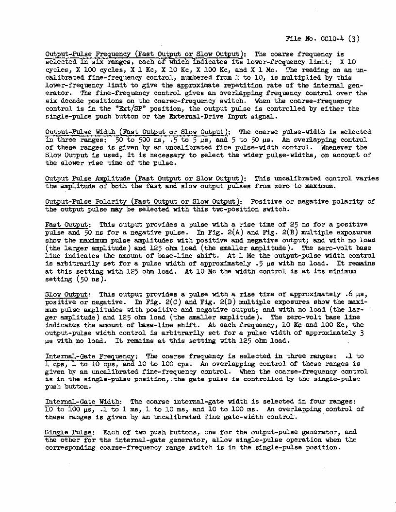
File No. CCl0-4 (3)
Output-Pulse Frequency (Fast output or Slow output): The coarse frequency is selected in six ranges, each of which indicates its lower-frequency limit: X 10 cycles, X 100 cycles, X l Kc, X 10 Kc, X 100 Kc, and X l Mc. The reading on an un-ca.J.ibrated fine-frequency control, numbered from l to 10, is multiplied by this lower-frequency limit to give the approximate repetition rate of the internal gen-era.tor. The fine-frequency control gives an overlapping frequency control over the six decade positions on the coarse-frequency switch. When the coarse-frequency control is in the "Ext/SP" position, the output pulse is controlled by either the single-pulse push button or the External-Drive Input signal.
_Qut;put-Pulse Width (Fast Output or Slow Output): The coarse pulse-width is selected in. three ranges: 50 to 500 ns, • 5 to 5 µs, and 5 to 50 µs. An overlapping control of these ranges is given by an uncalibrated fine pulse-width control. Whenever the Slow Output is used, it is necessary to select the wider pulse-widths, on account of the slower rise time of the pulse.
Output Pulse Amplitude (Fast Output or Slow output): This uncalibrated control varies the amplitude of both the fast and slow output pulses from zero to maximum.
Output-Pulse Polarity (Fast OUtput or Slow Output): Positive or negative polarity of the output pulse may be selected with this two-position switch.
Fast Output: This output provides a pulse with a rise time of 25 ns for a positive pulse and 50 ns for a negative pulse. In Fig. 2(A) and Fig. 2(B) multiple exposures show the maximum pulse amplitudes with positive and negative output; and with no load (the larger amplitude) and 125 ohm load (the smaller ampli tu.de). The zero-volt base line indicates the amount of base-line shift. At l Mc the output-pulse width control is arbitrarily set for a pulse width of approximately .5 µs with no load. It remains at this setting with 125 ohm load. At 10 Mc the width control is at its minimum setting ( 50 ns ) •
Slow Output: This output provides a pulse with a rise time of approximately .6 µs, positive or negative. In Fig. 2(C) and Fig. 2(D) multiple exposures show the maxi-mum pulse amplitudes with positive and negative output; and with no load (the lar-ger amplitude) and 125 ohm load (the smaller amplitude). The zero-volt base line indicates the amount of base-line shift. At each frequency, 10 Kc and 100 Kc, the output-pulse width control is arbitrarily set for a pulse width of approximately 3 µs with no load. It remains at this setting with 125 ohm load.
Internal-Gate Frequency: The coarse frequency is selected in three ranges: .1 to l cps, 1 to 10 cps, and 10 to 100 cps. An overlapping control of these ranges is given 'by an uncalibrated fine-frequency control. When the coarse-frequency control is in the sing1e-puJ.se position, the gate pulse is contro11ed by the sing1e-pu1.se push button.
Internal-Gate Width: The coarse internal-gate width is selected in four ranges: 10 to 100 µs, .l to l ms, l to 10 ms, and 10 to 100 ms. An overlapping control of' these ranges is given by an uncalibrated fine gate-width control.
Single Pulse: Each of two push buttons, one for the output-pulse genera.tor, and the other for the internal-gate generator, allow single-pulse operation when the corresponding coarse-frequency range switch is in the single-pulse position.
File No. CCl.0-4 (4)
Gate-Function Switch: When the gate is "on", it permits pulses to pass through f'rom the output-pulse generator to the output circuit. When it is "of'f'"', it blocks these pulses. · When the Gate-Function Switch is in the "Internal Gate" poEU.tion, the width and repetition rate of' the gate pul.se are determined by the settings of' the internal-gate width and frequency controls. When the Function Switch is in the "Ungated" position, the gate allows all pulses to pass through. In the "External Gate" position, a positive pulse of 18 volts minim:mn at the External-Gate Input connector is required to turn on the gate.
Gate-Polarity Switch: On-gate or off'-gate operation may be selected with this two-position switch. In the "+" position, the gate is on during the gate pulse. In the "-" position, the gate is off' durill$ the gate pulse.
Internal-Gate Out: This connector provides a gate pulse f'rom the internal-gate gen-era.tor for gating other equipment. When the gate is on, the de level is positive 20 volts. When the gate is off', the de level is zero volts. When the Gate-Polarity Switch is in the "+It position, the de level is positive 20 volts during the gate pulse. When the Gate-Polarity Switch is in the 11
-11 position, the de level. is zero
volts during the gate pulse.
External-Gate In: In the "External Gate'' position of' the Gate-Function Switch, a positive pulse of' 18 volts minimum at this connector w1l.l turn on the gate. Because the input signal is direct coupled to the gate, the length of the gate signal may be any desired length. There is no provision within the instrument f'or synchroniziDg the gate signal with the internal output~pulse genera.tor. Turn-on and turn-of'f' times of' the gate are approximately .2 µs f'or a step-function input.
External-Drive In: A positive signal at this connector will trigger the output-pulse genera.tor when the output-pulse coarse-frequency range switch is in the "Ext7SP" position. Specifications for this input are the same as for the Nanosecond Pulse Genera.tor in Counting Note CCl0-3.
Positive-Trigger OU.t: This output provides a positive pul.se f'or initiating timing or triggering an oscilloscope. Its amplitude is positive 15 volts at 100 Kc; down 5~ at l Mc. Its width is 50 ns. It precedes the output pulse by 30 ns at the lowest frequency and by 10 ns at the highest frequency.
CIRCUIT DESCRIPTION: See Fig. 3 and Fig. 4 for a schematic circuit diagram. The power supply and some details have been omitted f'or simplicity. For the complete schematic circuit dia.gram3 refer to print number 3X 5894.
The single-pulse and external.~drive signals trigger a square-wave genera.tor (Vl and V2) when the output-pulse coarse-frequency range switch is in the '*Ext/SP1
• position. In this position the square-wave generator is a monostable multivibrator,.whose pulse width and frequency are determined by the External-Drive Input, or singl.e-pulse signal. In the remaining six positions of' the coarse-frequency range switch, the square-wave generator is an astable multivibrator, whose coarse frequency is determined by the RC timing network. The fine-frequency adjustment returns the grid resistor to a variable potential that controls the frequency over a 10 to l range for any position of' the coarse-frequency range switch.
(A)
(C)
Fast output at l Mc. Top: positive output. Bottom: negative output. (Vertical sensitivity = 10 volts/cm; horizontal sweep = .1 µsec/cm).
Slow output at 10 Kc. Top: positive output. Bottom: negative output. (Vertical sensitivity = 20 volts/cm; horizontal sweep = .5 µsec/cm).
(B)
(D)
File No. CCl0-4 (5)
Fast output at 10 Mc. Top: positive output. Bottom: negative output. Minimum width control setting. (Vertical sensi-tivity = 5 volts/cm; hori-zontal sweep = .1 µsec/cm).
' Slow output at 100 Kc. Top: positive output . Bottom: negative output. (Vertical sensitivity = 20 volts/cm; horizontal sweep = .5 µsec/cm).
Fig. 2 - Output pulses. In each photograph, multiple exposures superimpose the following three conditions: no load (the larger amplitude), 125 ohm load (the smaller amplitude), and the zero-volt base line.
I 1.0I r~ I I GATE FREQUENCY GEN. I L _____ - -- - ____ _J
Fig. 3 - Circuit Diagram of the Gated Pulse Generator - Part 1
(,21<. IW
~ ...... CD
z 0 • (") (") ...... 0 I ~ -O' -
I - - - - - +1sov - - - - - - -1
FROM FIG. (3) A___.,,_....,....,._~~~-+
.001
I +ISOV I
V7A I Va6922 I
I I
,- - - +; ov- -I t-JSOV I I I I I I I I
1irso•• 1 J'ts' I
I I I
I 2sof'f I I 200.n I I - TRIGGER I L - - - - ~ - - - - - _ _J
+1sov
510 n 2.W -
1 - - -+iSov - - - - - - --, I I I I I .I
IM
IM
IMG13
1Nb'l3
f (FA!!T
; OUT) 10UTPUT 1POLARITY I SWliCM I I I
t--~~~--+~+------jr-+-0..'~ s B (s~
our) ,--~---- - - - +lov - - - - -, 1 +15011 I I
y../1 5--\ I
I I I I I I
L---~----
I I I
)\__I -v: ~~f ISLGWI .,__..___, OUT I
~~ -;- I SLOW I
OUTPUT 1 _________ J
Figo 4 - Circuit Diagram of the Gated Pulse Generator - Part 2
C1 C1 ...... 0 I ~ ---.I
File No. CCl0-4 (8) Similarly, the internal.-gate generator (Vl4) is a monostable multivibrator in the single-pulse position. Otherwise, it is an astable multivibrator. This generator triggers a monostable multivibrator which determines the gate-pulse width. On-gate or off-gate operation is selected after the phase inverter (V3), and the signal is passed on to a cathode follower output (V12).
The differentiated output of the square-wave generator is applied to the gate circuit (V4 and transistor 2N447). When the Gate-Function Switch is in the '~ngated't position, the base of the NPN transistor is returned to the collector and to a positive vol-tage. The transistor turns on a.lid allows V4 to conduct. In this state the gate is turned on. When the Gate-Function Switch is in either the "Internal. Gate" or 'tEx-ternal. Ga.te 0 positions, the transistor is biased -~JOnd cutoff by a fixed negative bias. The gatep then, is turned off. A positive gate signal from the internal.-gate generator, or from an external. source, will overcome this bias and turn on the tran-sistor and the gate.
The positive-trigger pulse is isolated and shaped by the circuit of v5.
The output-pulse width control (V6 and V7) is a monostable multivibrator which is triggered by the pulses passing through the gate from the output-pulse ge~erator.
Control of the output-pulse amplitude is achieved in the cathode of v9.
The polarity of the output pulse is selected after phase inverter V8, and the sig-nal is passed to both the fast output circuit (VlO and VlO .1) and to the slow out-put stage, where it is first amplified (Vll) and then coupled to cathode-follower V2C
REFEBENCES:
1. UCRL Drawing 3X 5894. 2. UCRL Counting Handbook, Counting Note CClO-3. 3. Personnel at UCRL, Berkeley Site, familiar with this unit: J. Hazelwood
(Counting Group ) •
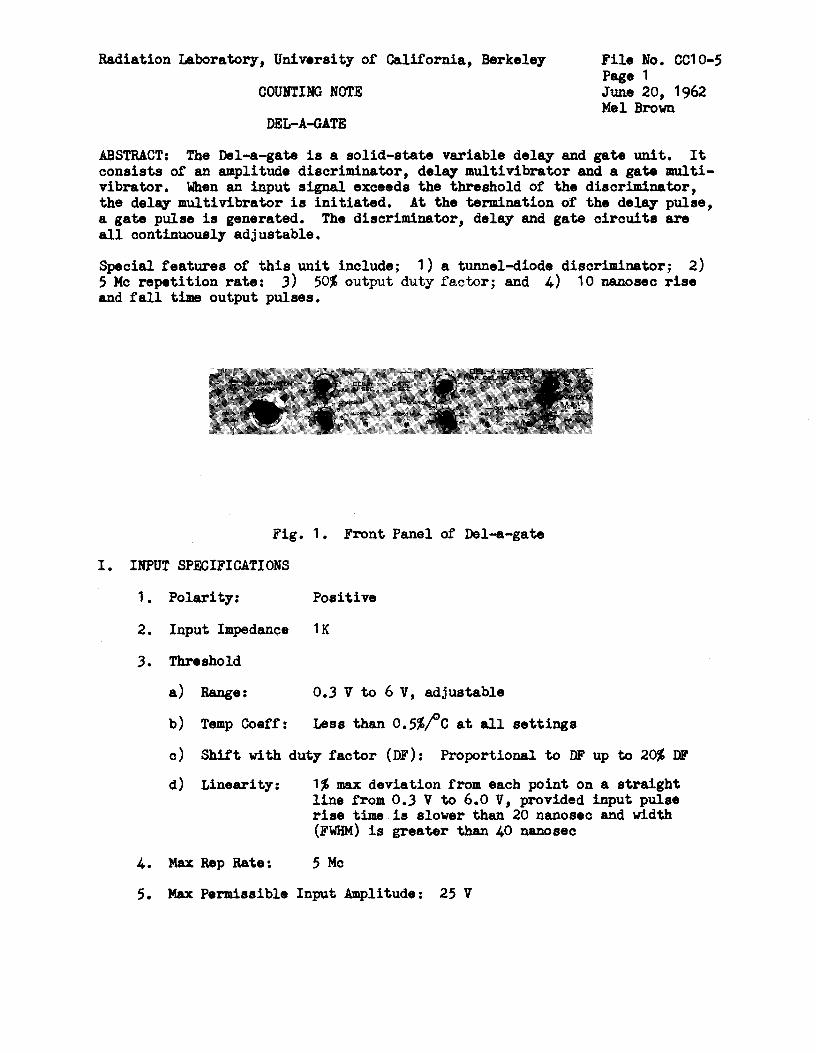
Radiation Laboratory, University of California, Berkeley
COUNTING NOTE
DEL-A-GATE
File No. CC10-5 Page 1 June 20, 1962 Mel Brown
ABSTRACT: The Del-a-gate is a solid-state variable delay and gate unit. It consists of an amplitude discriminator, delay multivibrator and a gate multi-vibrator. When an input signal exceeds the threshold of the discriminator, the delay multivibrator is initiated. At the termination of the delay pulse, a gate pulse is generated. The discriminator, delay and gate circuits are all continuously adjustable.
Special features of this unit include; 1) a tunnel-diode discriminator; 2) 5 Mc repetition rate: 3) 50% output duty factor; and 4) 10 nanosec rise and fall time output pulses.
Fig. 1. Front Panel of Del-a-gate
I. INPUT SPECIFICATIONS
1. Polarity: Positive
2. Input Impedance 1 K
3. Threshold
a) Range: 0.3 V to 6 V, adjustable
b) Temp Coaff: Less than 0.5%/'C at all settings
c) Shift with duty factor ( DF) : Proportional to DF up to 20% DF
d) Linearity:
4. Max Rep Rate:
1% max deviation from each point on a straight line from 0.3 V to 6.0 V, provided input pulse rise time is slower than 20 nanosec and width (FWHM) is greater than 40 nanosec
5 Mc
5. Max Permissible Input Amplitude: 25 V

II. OUTPUT SPECIFICATIONS
1 • Polarities: 2. Amplitude:
3. Output Impedance 4. Rise anf Fall Time: 5o Delay:
6. Gate: 7. Duty Factor: 8. Jitter:
III. POWER
1 • 105 - 125 VAC, 25 watts
IVo OPERATING INSTRUCTIONS
Pos and Neg simultaneously 6 V open circuit 3 V into 50 ohms 50 ohms
File No. CC10-5 (2)·
10 nanosec when terminated in 50 ohms 40 nanosec - 100 p.sec, continuously adjustable. Also zero delay position. 40 nanosec - 100 µsec, continuously adjustable 50% max (delay and gate multivibrators) Less than 0.1%
1. Input: The input impedance is set at 1 K ohms to avoid loading the input pulses. However, if the input rise time is less than 100 nanosec, reflections may occur and it may be necessary to terminate with a lower impedance.
The input is capacitively coupled so there will be a base line shift and change of threshold with increasing duty factor. The change of threshold, in percent, is proportional to duty factor up to 20%, beyond which the threshold changes more rapidlyo
2. Discriminator helipot: The helipot is calibrated in 0 - 10 major divisions. The 0 position corresponds to 0.3 v threshold, the 10 position to 6 v threshold. A calibration chart may easily be made · to translate helipot settings into volts. The accuracy of the Oo3 v and 6 v limits should not be considered better than + 5%, unless checked.
3. Controls: The COARSE delay and gate dials are marked to correspond to the approximate center of the range. The FINE controls provide continuous adjustment and overlap.
4. Delay monitor: A front panel delay MONITOR connector permits observation or use of the delay one-shot multivibrator waveform without interfering with the circuit timing. Its output impedance is 50 ohmso
5. Output connectors: To obtain clean .3 v pulses, with 10 nanosec rise and fall times~ it is necessary to use 50 ohm cable from the output connectors and ter-minate them in 50 ohms.
With unterminated outputs, the unit will supply 6 v pulses. The rise time will still be 10 nanosec; however there will be about 15% overshoot, and a fall time of about 70 nanosec, depending on the cable capacitance.
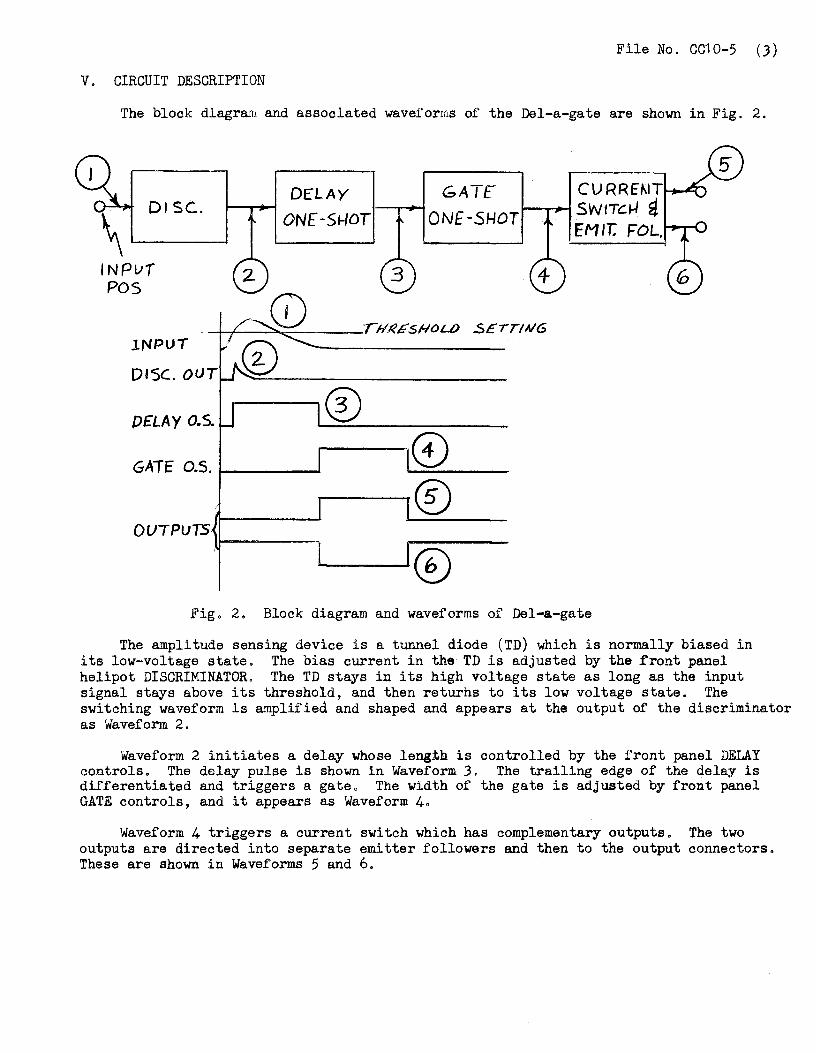
File No. CC10-5 (3)
V. CIRCUIT DESCRIPTION
The block diagram and associated waveforms of the Del-a-gate are shown in Fig. 2.
DI SC.. \......._ INPLlf POS
lNPUT
DISC. OUT
f)ELAY 0.5.
DELAY ONf-SHOT
GATE 0.5. ----
.------® OUTPUTS
Fig. 2. Block diagram and waveforms of Del•a-gate
The amplitude sensing device is a tunnel diode (TD) which is normally biased in its low-voltage state. The bias current in the TD is adjusted by the £rant panel helipot DISCRIMINATOR, The TD stays in its high voltage state as long as the input signal stays above its threshold, and then returhs to its low voltage state. The switching waveform is amplified and shaped and appears at the output of the discriminator as Waveform 2.
Waveform 2 initiates a delay whose length is controlled by the front panel DELAY controls. The delay pulse is shown in Waveform J. The trailing edge of the delay is differentiated and triggers a gate. The width of the gate is adjusted by front panel GATE controls, and it appears as Waveform 4.
Waveform 4 triggers a current switch which has complementary outputs. The two outputs are directed into separate emitter followers and then to the output connectors. These are shown in Waveforms 5 and 6.
File No. CC10-5 (4)
REFERENCES:
1 • DEL-A-GATE SCHEMATICS
a) Front Panel 4X540J
b) Power Regulator 4X5412
c) Timing Circuits 4X5424
d) Discriminator 4X543.3.
e) Assembly 4X6184
f) Block Diagram 5X4051
g) Check-Out Information 5X4041

~' '5\t:iiNA.L v INPUT" (Bt.tC..)
·~
~81,11>.."S +3.~"""'"" ~ se~s -~MA..MIN SENS
A¥ il&'1-.... "
1.e~ '""
'°"" ~~v
Fig. J.
.L IV
t
+n.v
e.1"-
IE5TP01tJT'"@ -. 7V MAX. 'S&.NS. -9.4VMIN.S&.NS
...,,,_ 1w,cc..
.....
\
.,...MAXIMUM SEN51T\VITY
~1---~ Jll.S:>J."
Discriminator Schematic Diagram
~--t-:r-t1-~~$~ ,...,
CR.I lN/&94 rtv 1sw
"""*~
0 0 ~
0 I
Vt -Vt -

\
r--------
-z.1 v
lOJ'+: 25V
-Z!V
750.!l.
' 3:-;/J.fl '
CJ::..1 iN/";, ..
L_.
ir1::r~ ·~ ~=t' •w
-ZIV
-ZIV
Fig. 4 - Delay and Gate Schematic Diagram
TGl·OffN - 1-fl. C\<::'.T. '
~l _J~ --:--E.1--.M,NA.T\ ';.-\lq S<).l
...... ;; __ ':_,
100-''
\ 0 0 ...... 0 I
\.1\ >
File No. CC 10-6 (1) January 13, 1964 H. G. Jackson
Lawrence Radiation Laboratory, University of California, Berkeley
COUNTING NOTE
DELAY GATE - 11X2461 P-1
I, SUMMARY This unit is useful for generating delay or gate signals using standard
4 V logic levels, 1 It takes the form of a multivibrator with complementary inputs and outputs. A selector switch allows the multivibrator to be oper-ated in the bistable mode; or one of six monostable positions covering the range 1 i1s to 1 s in decade steps. Fine control of the pulse width is obtained from a potentiometer mounted concentric with the selection switch.
Dual 110R 11 inputs are provided on both the SET a:id RESET inputs. The multivibrator may also be manually SET or RESET by means of a push-button. A light indicates when the multivibrator is in the SET position. A toggle switch is provided to inhibit signals into the -unit; in the OFF position the multivibrator is automatically RESET.
The unit is packaged in a shielded nanobox. A size 4X box (3 x 5-1/4" panel) is used.
DELAV GATE , ... ,.., .. 1
ON R
OFF
~ • • R
s
IN
llX2460PI
Fig. 1 - Delay Gate -- Front View
1See CC 5-9 for logic voltage levels.
II. SPEQIFICATIONS Inout
HGJ:mt
Impedance 111 11 Level 110 11 Level
Min. Width Max. duty cycle
Delay/Gate Widths Bistable
1 K Q +4 v -1 v 30 ns 90 %
1 µS - 10 µs 10 µs - 100 µs
100 µs - 1 ms 1 ms - 10 ms
10 ms - 100 ms 100 ms - 1 s
Power Reauired +12 V 70 mA (120 mA max.) -12 v 20 mA Ground
Output Impedance
"l ti 110 II
Delay Rise-time
pin 10. pin 21. pin 1.
cc 10-6 (2)
< 50 Q (50 mA max.) +4 v -1 v
< 15 ns < 15 ns for step input
Pt:?.s/?/P/11 I 81.S7"48L£ C/ = 41,,,r. - 111/C,q % .t.u.s •N/,.,S CZ. : .tlll$s.,µT. · MJ't.4.R .3 /Ops - /t?~' ~,! : .t?,3Jpr 4 /Pftvs - /ms : C4 = '°·'J,u~ 3SY. rA. .s ;,.,.,. ... /'7"7,s : C5 : .3 . .Jpr. 6 ltl>hs • /OP-,,,,s: It" : .S.J,.uf: /OK 7i4. 1 /Ptl "".S - /.soc..; ,, ::' .3Jq.,.,£ 6Y. rA
~12 //
~I
-1.Z //
~It. 330./L
~4 2#4.H·
,ti!/.$ 820..0.. ~,..,,
-. /2 JI
,R/5 25k
RI? azoA. ~
t:.7
-7
a
I
- - - -' S4·'4
Delay Gate Schematic
}
..s 4- I/I#:/"!,, 7 ~IT/oA/
.SWl?"CH (3 5.-¥ow"") COARSE DELAY
+l2V
-+IZV
+
-/2¥' '-------1>
0 0
....... 0 I O'
1
File No. CC 10-7 (1) January 14, 1964 H. G. Jackson
Lawrence Radiation Laboratory, University of California, Berkeley
COUNTING NOTE
RELAY DRIVER - 11X2431 P-1
I. SUMMARY A bistable circuit is used to operate a mercury-wetted contact relay
in two modes: 1. The relay is energized by application of a standard +4 V logic
level1 to the SET input. The relay will stay energized until the bistable circuit is reset by a +4 V logic level at the RESET input.
2. The relay can also be energized by applying a +4 V logic level at the INPUT. Here the relay will stay energized only during the interval of time that the 111 11 input is present.
The relay contacts (SPDT) are brought to the front panel and also to the rear connector.
The relay contacts should be protected in accordance with the chart sho'Wil in Fig. 2. Information from c. P. Clare Co., Catalog 201-A. The maximum contact rating is 2 A or 500 V.
The unit is packaged in a shielded nanobox. A size 3X box (2-1/4 x 5-1/4" panel) is used.
• •• 11X24H P1
Fig. 1 - Relay Driver -- Front View
See CC 5-9 for logic voltage levels.
cc 10-7 (2)
II. ~PEQIFICATIONS
Input Bistable InmJ.t Impedance 1 K Q 1 K Q
"l" Level +4 v +4 v 110 11 Level -1 v -1 v
Min. width 100 ns 3 ms Max. rate 180 pps 180 pps Relay Contacts Common pin 16.
NC pin 17. NO pin 18.
Power Reguireg +12 v 60 mA pin 10. -12 v 4 mA pin 21. Ground pin 1.
HGJ:mt
cc 10-7 (3)
90o----+~+-~-+'l~~~......,-Hif-Hi-\--+--t--t~--+--t--+--t--+-li-t+--H-++-+++-l---+--ll--l--l---+---,lf.-l--+-+-ll,9
800 .8 roo J 600 ~
500 .5
300---+-
I 0 0 l=:::::i::=:;l:::=11=t=f::::t=1=!= 90t:==t:::::::1=1~=1=+=1=t= BOl==f:::::::il==ir=f=F=Fi=t=:F
Cf) 70l==l:==t=t=t::=t:::t:::t=t:::t=t: ::::E60----+-+-~-+-+-i-+-+++-t++-+H~-+--t-+-+--+-~~
::c: 050
.4
.I .09 .08 .o·r .06
.05
Cf)
Cl <( a::: <( LL. 0 a::: 0
::::E
I 40
w 30 0 :z <(
MERCURY WETTED CONTACT RELAY .04 w 0
-1--1--+-+-.0 3 :z
..... 20 Cf)
Cf) 15 w a:::
10 9 e
6
4
1.5
CONTACT PROTECTION NETWORK
<( ..... -i--i--+-+-11.02 0
<( a..
-+-+-H--+--+-¥-t1-l-~+-l-~~1---1---1---+--l---+--+--+--i--..015 <(
I 2 C = 10 MFD
FOR E < 10, R MAY BE 3X INDICATED
70< E < 100, R MAY BE ::!:50% 100< E < 150, R MAY BE ± 10%
E > 150, R MAY BE ± 5%
RMINIMUM =0.5 OHM CMINIMUM =.001 MFD.
.008
-H*'+l'lr+-'r--+--"r+--t--+--+--+--+--+-+-... 006 ++~--t--+-+-+-+-+-++-ttv+l~~-+--'\-
+-+--+-+-+-+-++-++++t-H-+-~-+T+-+---!-+-+--+-+-9 .00 5
0
, ..... _ ................................. _ .............. _ ...... _...... ... ....... _ ........................ 001 .02 .03 .04 .05 .06 .07.08.09.1 .15 .2 .3 .4 .5 .6 .7 .8 .9 1.0 1.5 2.0 3.0 4.0 5.0
CURRENT AMPERES Courtesy of C. P. Clare & Co. (IMMEDIATELY PRIOR TO CONTACT OPENING)
Fig 2. - Contact Protection Network
@--~
A'7 /O,.,
+ CJ -T.6.s..f ,+,35¥
"' Sil--------'
.r1 1 .rl.IPl/.r>P
M,OPVI.£
Relay Driver Schematic
0 0
...... 0 .!:i

1
File No. CC 10-8 (1) January 13, 1964 H. G. Jackson
Lawrence Radiation Laboratory, University of California, Berkeley
COUNT! NG NOTE
PULSE GENERATORS 11X2451 P-1 and 11X2451 P-2
I. SUMMARY These units are useful in simulating the 184" Cyclotron and Bevatron
repetition rates as well as a 1 pps and a 106 pps rate. The 11X2451 P-2 unit has an improved oscillator; the operating specifications are the same on both units.
The pulse frequency is determined by an astable multivibrator, and the pulse width by a monostable multivibrator. These are followed by a pulse amplitude control and parallel NPN-PNP output emitter-followers.
Selection is made on one of four pulse frequency positions. A fine control concentric with this selector switch allows the frequency to be varied at least ± 50%. An EXTERNAL frequency source may also be used.
Pulse width selection is from 100 ns to 1 s in seven decade steps. Fine control of the pulse width is by a potentiometer mounted concentric with the pulse width switch.
The amplitude control allows the pulse amplitude to be varied from 0 to +4 V. When
1set to maximum amplitude, the unit generates a standard
+4 V logic level. The unit is packaged in a shielded nanobox. A size 4X box (3 x 5-1/4"
panel) is used.
Fig. 1 - Pulse Generator -- Front View
See CC 5-9 for logic voltage levels.
cc 10-8 (2)
II. SPECIFICATIONS
HGJ:mt
Ext, Input Impedance Trigger Level Rise-time
Pulse Frequency Off External 10 ppm
1 pps 606pps 10 pps
Power Required
1 K Q +4 v
< 1 µs
Output Impedance Amplitude Rise-time
Pulse Width
< 50 Q (50 mA max.) Variable 0 to +4 V < 15 ns
100 ns - 1 µs 1 µs - 10 µs
10 µs - 100 µs 100 µs - 1 ms
1 ms - 10 ms 10 ms - 100 ms
100 ms - 1 s
+12 V 70 mA (120 mA max.) pin 10. -12 V 35 mA pin 21. Ground pin 1.
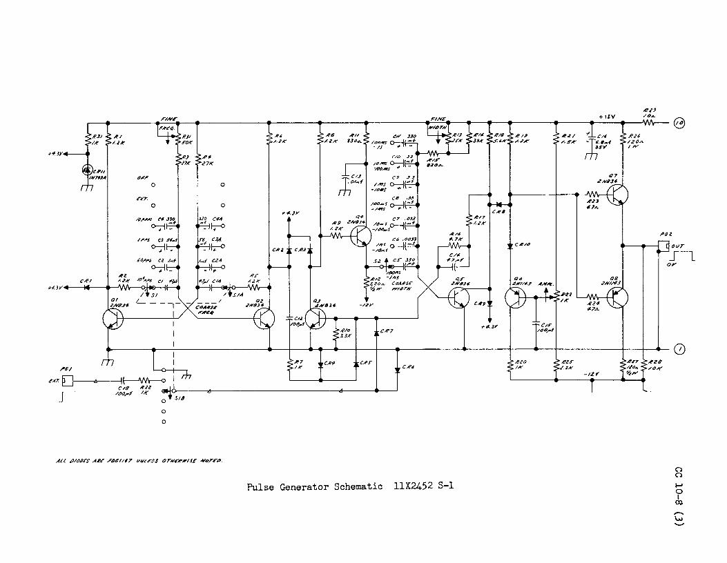
l'GI
It I /.lK
0
0
exr. D--.,.,,ti---llf;----AM--o C/ll A!.12
/OO,,.:f ht' 0
0
0
0
0
SIB
QZ .?NB.14
.('I /.2K
RB /.ZK
A!I/ 3.14.A
C/O .13
/""" o-:-l f "AIOA1$ 'fll -
C9 J.3 / AIS o-::.1 ,,.,. 7
-/"""' ~ -cs .3.$
~°:'~r o-;-1 -_~ e7 .DV
::~ro---i --F
C6 .oo,1 _:;:r o--1 -:1
COAA'SC WIP7".H
-/ZY
RIO J.3K
CR7
CR«
Pulse Generator Schematic 11X2452 S-1
+IZV
CA!B
l'O Z
0
(') (')
....... 0 I
CXl
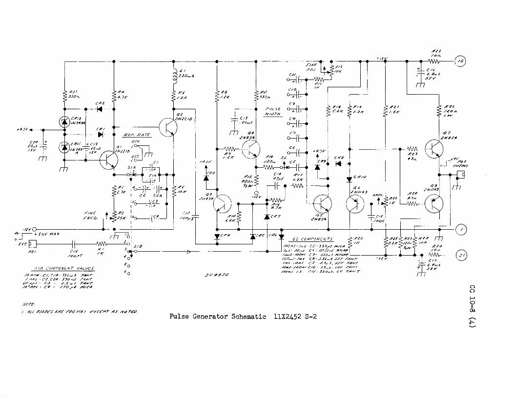
Ci!O t-<i'i!~f r /ff r-h
F//VC: FR€Q.
SIA COMPOIVCNT VALVcS
/0,1/'-"·C/,Cl-4-530~.7 TA,vT / ,P',,••s - Ci?, C2A - 330.-:f T,,,.A/T
60//f · CJ .?.2.-J TANT /t? ",,P"'1'f - C9 - /.5"0 /4- M/t"A
#OTc."
/ AU P/CJPcS .-IA'e .FPG/1117 E¥CC/T ,,,_, ,Yt:JT<!"P.
C/I
~-ft'I/
C/0 R8 o-;;-j /.<'A: 5.Jo.,..
C9 Pl/L 5 E: 0--;L-j JYJiJTH
C1J ca ~.Ol~i o-;;-J
(;?q
~ .?A/831-
C6
£/? .Si! o-j
Pulse Generator Schematic 11X2452 S-2
CR8 c "!9._--4.-•
0 0 I-' 0 I
00
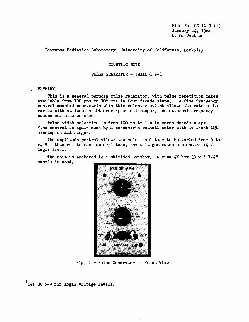
File No. CC 10-9 (1) January 14, 1964 H. G. Jackson
Lawrence Radiation Laboratory, University of California, Berkeley
COUNTING NOTE
PULSE GENERATOR - 18Xl051 P-1
I. SUMMARY This is a general purposg pulse generator, with pulse repetition rates
available from 100 pps to 10 pps in four decade steps. A fine frequency control mounted concentric with this selector switch allows the rate to be varied with at least a 10% overlap on all ranges. An external frequency source may also be used.
Pulse width selection is from 100 ns to 1 s in seven decade steps. Fine control is again made by a concentric potentiometer with at least 10% overlap on all ranges.
The amplitude control allows the pulse amplitude to be varied from 0 to +4 V. When set to maximum amplitude, the unit generates a standard +4 V logic level.1
The unit is packaged in a shielded nanobox. A size 4X box (3 x 5-1/4" panel) is used.
PULSE GEN.
Fig. 1 - Pulse Generator -- Front View
1See CC 5-9 for logic voltage levels.
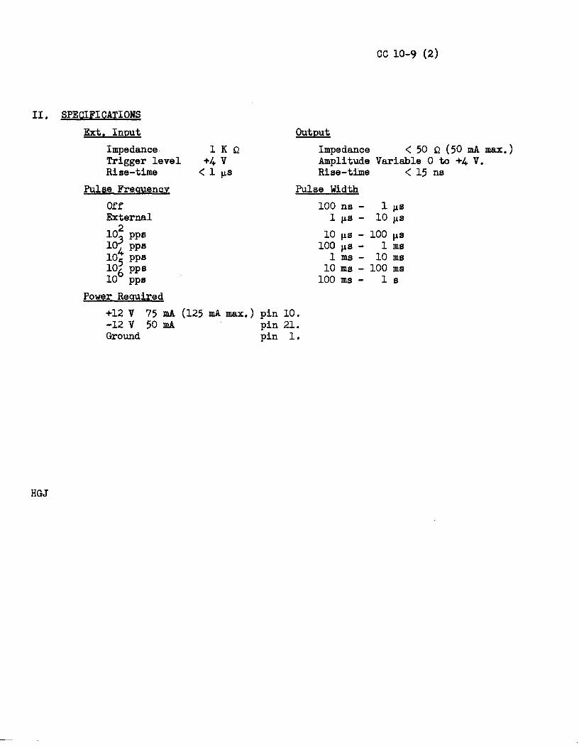
cc 10-9 (2)
II. SPECIFICATIONS
HGJ
Ext. In.wt Impedance Trigger level Rise-time
Output 1 K Q
+4 v < l µs
Impedance < 50 Q (50 mA max.) Amplitude Variable 0 to +4 V. Rise-time < 15 ns
Pulse Frequency Off
Pulse Width
External 2 103 pps
104 pps 105 pps io6 pps 10 pps
Power Required +12 V 75 mA (125 mA max.) pin 10. -12 V 50 mA pin 21. Ground pin 1.
100 ns - 1 µ.s 1 µs - 10 µs
10 µs - 100 µs 100 µs - 1 ms
1 ms - 10 ms 10 ms - 100 ms
100 ms - 1 s
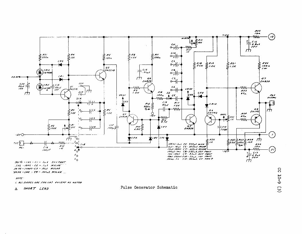
IKC -IOKC - CZ -./_f' MY.tA~
/0 A'C - /dt>A""C- CJ - . Ol~f' M Y•AA'
'OOA'C -h'•IC - c• - ,Ool-f MY'-AK
lltJT[
/, A.!( ,P/0.PcS ~,Pe FPG/lft7 r.;cr,,T A.S ,YQT<,P
.SHORT LEAIJ
R.>
RI(
l.2A'
<./'2 /oo,...
~ C/O
R8 ,(',// o-;-1 /ht,' JSOJL
C!I
~ Cll ce l.0/-i ~
<11-~ .!Nl/Jf.
H.3Y
CRS
Pulse Generator Schematic
- A!'/S-/K
.-.~JY
CK!I
Q.r ~N6'J~
,t'/J
,t'/6 S:'"f
'"'"
,t';f
1-l'f
(") (")
....... 0 I -.c
File No. CC 10-lOA (1) June 30, 1966 George Constantian
and Ken Bregger
Lawrence Radiation Laboratory, University of California, Berkeley
COUNTING NOTE
HIGH-VOLTAGE POWER FOR MULTIPLIER PHOTOTUBES
I. POWER SUPPLIES
Table I indicates the manufacturers' specifications for high-voltage power supplies in current use at LRL. These units are checked to meet LRL specifications in effect at the time of purchase.
II. POWER DISTRIBUTION
A. Resistive Dividers.
Where load regulation is not a problem, resistive dividers may be used in distributing power from one source to several phototube bases.
Fig. 1 indicates a typical 5 kV, 4-channel high-voltage divider panel. At 5 kV, no load, it permits a 600 V adjustment in hv outputs. Each output may be switched off individually. Up to 3 milliampers may be taken from each output without damage to the unit. Each divider panel draws 4 mA from the supply at 5 kV, no load. A switched meter output permits the monitoring of any output with an external meter.
A 3 kV, 4-channel divider is also available. At 3 kV, no load, the output may be varied by 500 v. Up to 3 milliamperes may be taken from each output without damage to the unit. Each divider panel draws 4 mA from the supply at 3 kV, no load. A switched meter output permits the monitoring of any output with an external meter.
B. Zener Dividers.
For better load regulation a zener diode divider is available (Fig. 2, 3). This high-voltage divider has twenty separate outputs, each individually adjustable by increments of 20 volts from the power supply voltage to 580 volts below the supply voltage. The divider is designed to supply currents from 0 to 40 ma. A 50 ma meter is mounted on the front of the unit for continuous monitoring of total load current (Red-lined at 40 ma as a limit reminder).

CC 10-lOA (2)
Either positive or negative high voltage can be used by plugging the positive or negative voltage source into the appropriately marked input jack on the rear of the unit, and inserting a pair of shorting pins at the proper level in the ammeter reversing circuit. The load can be distributed in any desired combination totaling 0 to 40 ma, provided no single output exceeds 15 ma. This is a reasonable limit for the dissipation level in the 1/2 watt lK ohm surge limiting resistor in series with each output. The power source must, of course, match the polarity• maximum voltage• and maximum current requirements of any intended usage. A 3 KV• 40 ma supply is recommended; 6KV is max.
Output voltages are supplied to an array of twenty marked high voltage connectors on the rear of the unit. The twenty columns of the front panel matrix correspond to the outputs. The thirty rows of this front panel matrix correspond to the supply voltage and successive 20 volt increments below the supply voltage. Output voltage selection is accomplished by "Switching In" the proper voltage by means of a shorting pin with an insulated handle inserted into a hole with the appropriate coordinates on the matrix board. Adjustment is accomplished by moving vertically in the column corresponding to the output to be adjusted by the desired number of 20 V increments (Rows). It is recOlllillended that output voltage adjustment be made by using two shorting pins in a "leap frog" manner in order to avoid disconnecting the load entirely whenever a pin is pulled. Note, however, that while two pins are inserted in the same column the zener diode between the two is shorted out - the voltage being that of the higher (absolute value) of the two. Thus in adjusting one output in a "leap frog" manner• momentary 20 volt changes will occur in all other outputs set to levels below the higher (absolute value) of the two "leap frog" pins.
Provision is made on the front panel for externally monitoring the voltage supplied to any selected output by "Switching In" an external voltmeter. This is accomplished by connecting an app~opriate meter to the external meter jack and inserting a pin in the receptacle directly below the column for which the voltage is to be monitored.
Output load regulation can be estimated for any circumstance by use of the following relationship. !:J.E/ma/row zener diode = 0.035 volts." This results in a worst case !:J.E of approximately 1 volt ma load change in row 30.
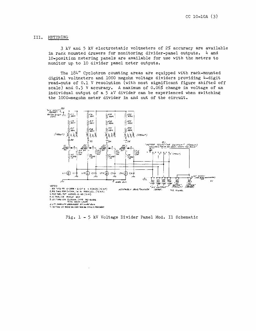
CC 10-lOA (3)
III. METERING
3 kV and 5 kV electrostatic voltmeters of 2% accuracy are available in rack mounted drawers for monitoring divider-panel outputs. 4 and 10-position metering panels are available for use with the meters to monitor up to 10 divider panel meter outputs.
The 184" Cyclotron counting areas are equipped with rack-mounted digital voltmeters and 1000 megohm voltage dividers providing 4-digit read-outs of 0.1 V resolution (with most significant figure shifted off scale) and 0.5 V accuracy. A maximum of 0.06% change in voltage of an individual output of a 5 kV divider can be experienced when switchin~ the 1000-megohm meter divider in and out of the circuit.
LT[ • C~ LTZ.
NOTE'S: l. 1<15 Tl-H<:u RB 41138.::IK + 6ic511 K IN 5E.RIE'5.(1Yo M.f.) Z,RI?> now R.?4 e11t96K, lW IN PARALLE.L. (l"i.M.~.)' 3, PG2 T"RU P67 A~SI02· IO·l"S (10 KV) 4.Cl n.i~u C4 1500pf 6KV 5. LTl T~l'.U LT4 E.LDE.MA TYPE IBZ-b096
WITM NC.2H LAMP, ~LT"/ 7"N4-'~N 41t:'UNPI£) LSYw,,,ec LSVS 7. SZ. TH~U '.>4 ~ADIO SW. CORP: MOD.9'..IST'l'LE A NOl.J.SHORT
Fig. l - 5 kV Voltage Divider Panel Mod. II Schematic
SU
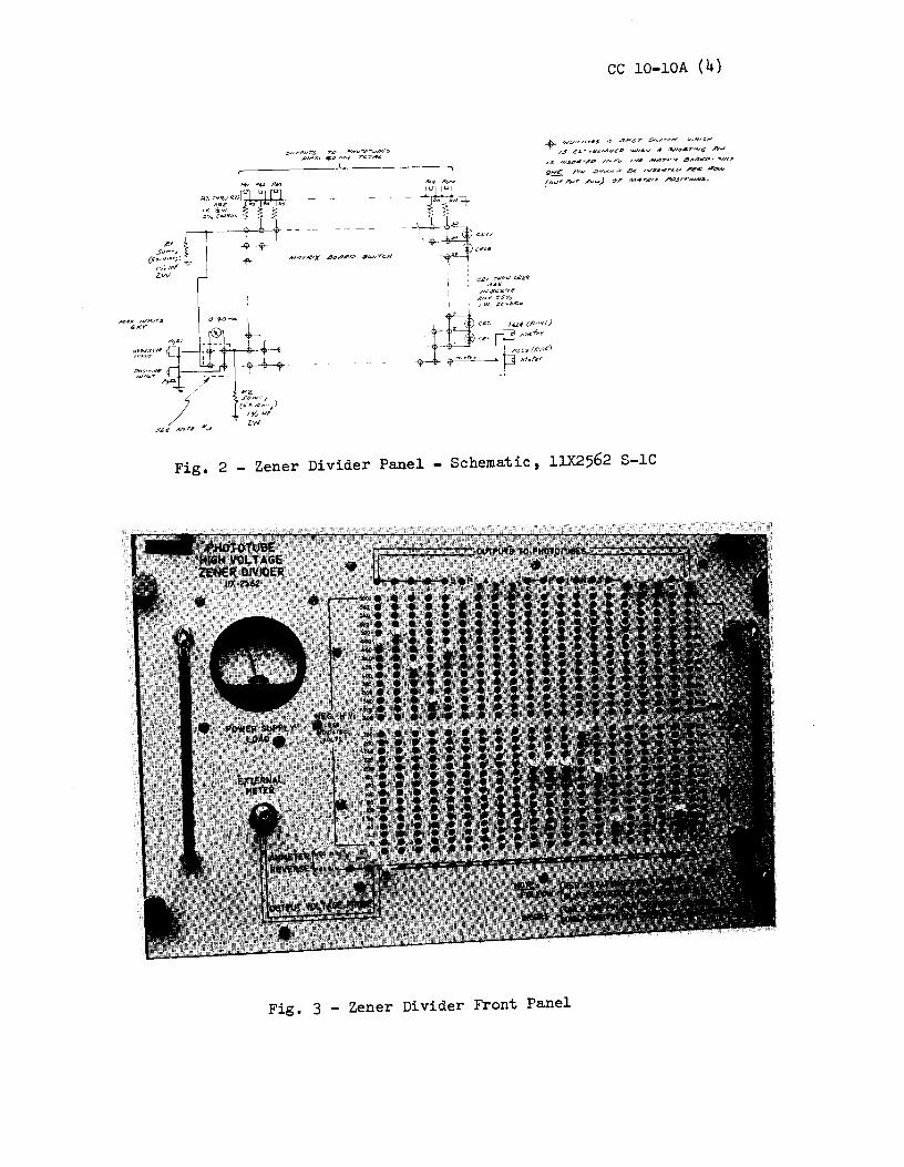
,el 50-·;
(.SJ<l0"'4~) 1%1"/ 2W
Fig,
"'" ..ro-'r (JtX ,10,._,.))
tY., VIF
' Zw
7<:; P#,;>TPT~4'65 4-,;;N/,-/ T"()TAL
CC 10-lOA (4)
+ /;</0H""HT£S "1 .:5P.::;r S4>17t:"I¥' "'-'''hC;.I
/..$ L:!-- ,/,UJ.S#C-D WN~V ;f $).lt;U~ . .,../IV(; Pl-.J
1.S /A./.$4~"'Ji£,D /Nro:> 7,N.G MA?A"'-f' $,;;A.-!'P· e>;</,&Y
Q!:t!E. P1-v .::;•1~.t P B<t! ;,.;54~r~.o ~JI! ~
(01J1"PJJr ~,., ..... ) or M,.,.,.,eo1 ,Pr;l~/r,~.
2 - Zener Divider Panel - Schematic, 11X2562 S-lC
Fig, 3 - Zener Divider Front Panel

N.E. SCIENTIFIC MFR. & MODEL MOD. RE-3002.EW
VOLTAGE ± 0.5 kV to ± 3 kV
CURRENT 0-20 mA
LINE REGULATIO~ ± .005%
LOAD REGULATI O; ± .005%
STABILITY ± .005%/Hr. ± .05%/Day
TEMP. COEFFICIENT
RIPPLE & NOISE 2 millivolts p-p
4-500 V Steps VOLTAGE CONTROLS 10-50 V Steps
1-60 V Vernier
VOLTAGE RESOLUTION3
VOLTAGE ACCURAcx4 + 2%
INPUT 105-125 V ao 60 CPS 130 W
PANEL HEIGHT 8-3/4"
CHASSIS DEPTH 12-1/2 11
REMARKS
TABLE I
1105 V to 125 V. 2 No Load to Full Load Except as Noted.
N.E. SCIENTIFIC MOD. RE-5001EW
± 0. 5 kV to ± 5 kV
0-10 mA
+ .005%
+ .005%
± .005%/Hr. ± .05%/Day
2 millivolts p-p
8-500 V Steps 10-50 V Steps 1-60 V Vernier
± 2%
105-125 V ac 60 CPS 125 W
8-3/4"
12-1/2 11
3The guaranteed minimum increment of output voltage adjustment.
CC 10- lOA ( 5 )
2X6314
± 0. 5 kV to ± 3 kV
0-20 mA
± .005%
+ .005%
± .005%/Hr. ± .05%/Day
2 millivolts p-p
4-500 V Steps 10-50 V Steps 1-60 V Vernier
+ 2%
105-125 V ac 60 CPS 130 W
8-3/4"
12-1/2 11
4The aoouraoy of the output voltage indicated by the sum of the dial settings.
·-

CC 10-lOA ( 6)
JOHN FLUKE MFR. & MODEL MOD. 408 A/U NJE MOD. 64H40 CARAD MOD. 1524A
VOLTAGE ± 0.5 kV to ± 6 kV ± 0.5 kV to ± 5 kV ± 0.5 kV to ± 3 kV
CURRENT 0-20 mA 0-20 mA 0-20 mA
LINE REGULATION ± .01% ± .01% + .0001%
LOAD REGULATION ± ,01i + .005% 10 mA Step
± .001% + 20 mV .
.005!1>/Hr. ± .005%/Hr ± .005%/Hr. STABILITY ± ± .03%/Day ± .05%/8 Hr. ± .05%/10 Hr.
TEMP. COEFFICIENT .
RIPPLE & NOISE 5 millivolts rms 5 millivolts p-p 1 millivolt rms
5-1000 V Steps VOLTAGE CONTROLS 9-100 V Steps 8-500 V_Steps 4-500 V Steps
10-10 V Steps 9-50 V Steps 10-50 V Steps 1-10 V Vernier 1-60 V Vernier 1-60 V Vernier
VOLTAGE RESOLUTION 10 millivolts
VOLTAGE ACCURACY + 0.25% + 2% ± 1% of Dial Setting
INPUT 117 v 50/60 CPS 105-125 V ac 105-125 V ac 250 w 60 CPS 350 W 60 CPS 210 W
PANEL HEIGHT 8-3/4" 8-3/4" 8-3/4"
CHASSIS DEPTH 15" 17-3/4" 14-5/8 11
Interlock latching Units must be relay prevents mounted to allow starting the instru- 1-3/4 11 (one W.E.
REMARKS ment with the XlOOO rack unit) above & switch in other thar below for air cir-the 500 or 1000 culation. positions.
TABLE I (Cont. )

CC 10-lOA (7)
MFR. & MODEL CA RAD MOD. 1522 POWER DESIGNS POWER DESIGNS MOD. 1544 MOD. 1556
VOLTAGE ±.5 kV to ±5kV ±lV to ±3kV ±lV to ±6kV
CURRENT 0-20 mA 0-20 mA 0-20 mA
LINE REGULATION ±.001% ±.001% + 2mV ±.001% + 2mV
LOAD REGULATION 10 mA Step ±.001% + 20mV ±.001% + 2mV ±.001% + 2mV
STABILITY ±.005%/Hr. ±,005%/Hr. ±. 005%/Hr. ±.05%/10 Hr. ±.03%/24 Hr. ±.03%/24 Hr.
TEMP. COEFFICIENT 25 ppm/QC 25 ppm/QC
RIPPLE & NOISE 1 millivolt rms 2 millivolts PP 2 millivolts p-p
8-500 V Steps 5-500 v Steps 5-1000 V Steps VOLTAGE CONTROLS 10-50 V Steps 4-100 v Steps 9-100 V Steps
1-60 V Vernier 10-10 v Steps 10-10 V Steps 1- 12 V Vernier 1-12 V Vernier
VOLTAGE RESOLUTION 10 millivolts 10 millivolts
VOLTAGE ACCURACY ±1% of Dial Setting 0. 25% above 250 v 0. 25% above 250 v
INPUT 105-125 v ac 105-125 v ac 105-125 v ac 60 CPS 300 •w 50 to 400 CPS 130 w 50 to 400 CPS 200W
PANEL HEIGHT 8-3/4" 5-1/4" 8-3/4"
CHASSIS DEPTH 14- 5/8" 16" 16"
Electronic overload Electronic overload REMAR~S protection protects protection protects
supply in case of supply in case of momentary or indef- momentary or in def-inite overload or inite overload or short circuit. short circuit. Reset not required. Reset not required.
TABLE I (Cont.)
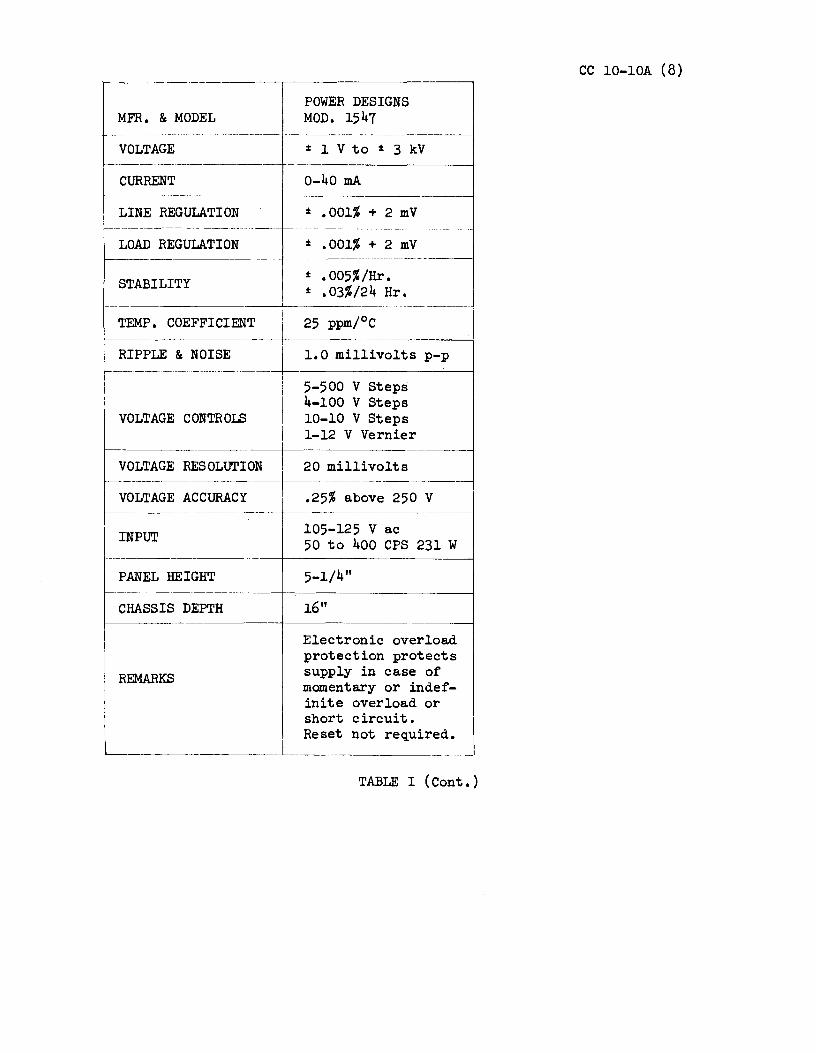
------··-----·----,--·
MFR. & MODEL POWER DESIGNS MOD. 1547
---·------- -----------------------;
VOLTAGE :t 1 V to :t 3 kV
CURRENT 0-40 mA
LINE REGULATION :t .001% + 2 mV
LOAD REGULATION :t .001% + 2 mV ----------
STABILITY :t • 005%/Hr. :t .03%/24 Hr. j
------------------'---~ 25 ppmf-~~-------------1 TEMP. COEFFICIENT
------- ---------- --------
!SE I 1.0 millivolts I RIPPLE & NO p-p --------·· ------+--
! 5-500 v Steps I
I 4-100 v Steps
TROLS 10-10 V Steps I 1-12 V Vernier
VOLTAGE CON
OLUT;~---t-20 millivolts --
VOLTAGE RES ------·-----
VOLTAGE ACC URA CY ---
I INPUT
T -·
[
PANEL HEIGH -----·- ·------·--
CHASSIS DEPT
I I
REMARKS
H
-------------------.25% above 250 v
-------
105-125 V ac 50 to 400 CPS 231 w 5-1/4"
16"
Electronic overload protection protects supply in case of momentary or indef-inite overload or short circuit. Reset not required. ______ L __________ ~ -- - -~---------
TABLE I (Cont.)
CC 10-lOA (8)
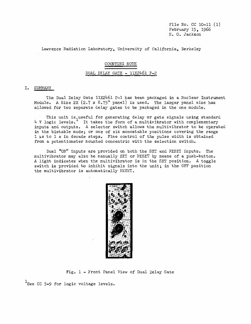
File No. CC 10-11 (1) February 15, 1966 H. G. Jackson
Lawrence Radiation Laboratory, University of California, Berkeley
COUNTING NOTE
DUAL DELAY GATE - 11X2461 P-2
I. SUMMARY
1
The Dual Delay Gate 11X2461 P-1 has been packaged in a Nuclear Instrument Module. A Size 2X (2.7 x 8.75" panel) is used. The larger panel size has allowed for two separate delay gates to be packaged in the one module.
This unit is1useful for generating delay or gate signals using standard 4 V logic levels. It takes the form of a multivibrator with complementary inputs and outputs. A selector switch allows the multivibrator to be operated in the bistable mode; or one of six monostable positions covering the range 1 µs to 1 s in decade steps. Fine control of the pulse width is obtained from a potentiometer mounted concentric with the selection switch,
Dual "OR" inputs are provided on both the SET and RESET inputs. The multivibrator may also be manually SET or RESET by means of a push-button. A light indicates when the multivibrator is in the SET position. A toggle switch is provided to inhibit signals into the unit; in the OFF position the multivibrator is automatically RESET.
Fig. 1 - Front Panel View of Dual Delay Gate
See CC 5-9 for logic voltage levels.
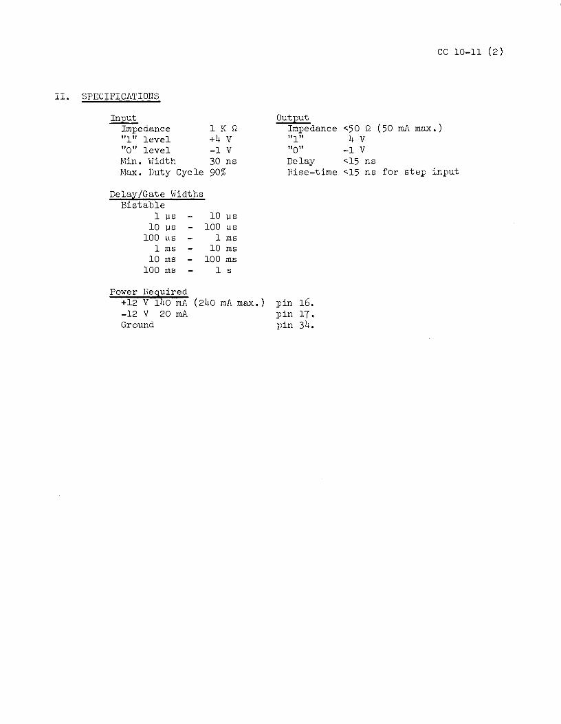
II. SPECIFICA'l'IONS
Input Impedance "l" level "O" level Min. Width Max. Duty Cycle
Dela~/Gate Widths Bistable
1 µs 10 µs
100 µs 1 ms
10 ms 100 ms
Power Required
1 K S1 +4 v -1 v 30 ns 90%
10 µs 100 µs
1 ms 10 ms
100 ms 1 s
+12 V 140 mA (240 mA max.) -12 v 20 mA Ground
Output Impedance "l" "O"
cc 10-11 (2)
<50 S1 (50 mA max.) 4 v
-1 v Delay <15 ns Rise-time <15 ns for step input
pin 16. pin 17. pin 34.
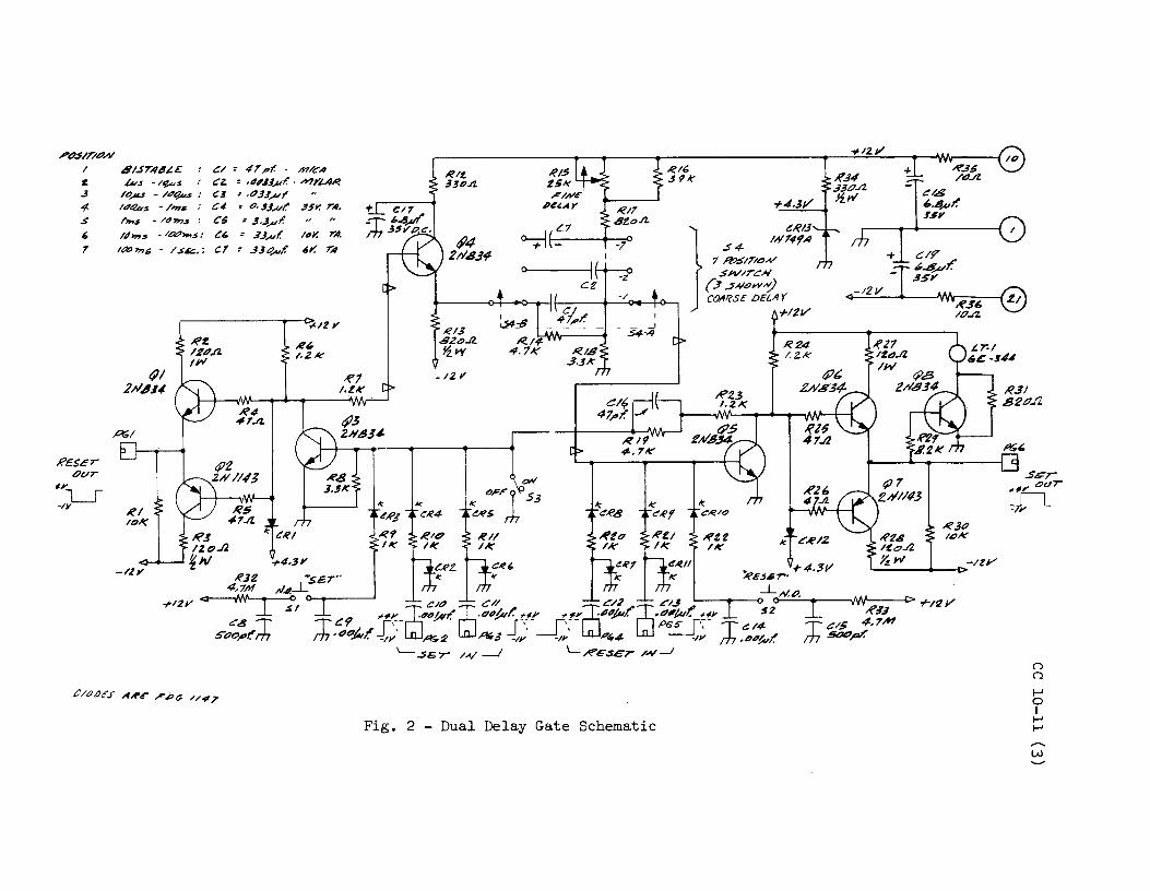
Pt7S/7/PAI I $/.S/46L.C z. .3 4 .s 6 1'
.tu.s /O,u.s 1"14,qs /,.,,s
111>,,,. /PO >n$
p;;
~/ ID.I(
-/211'
.. 1q,,,us - /"14Ms :
- /ms : .. /d7'n.s :
- la::>,..,.s: - /ssc..:
C/ = 47_,.t: - m/C4 CZ. : dlll.J.l_µf. · MJ'.t./J~ C.J : .'7.3.J,,u I' C4 = o . .JJ,.vt' .3SY. 7'19. C5 : .J,.J~I: C'- : s..J,,.,f. lo//. 7'11. ,, : 3317,uf.' 6Y. 1:<I
,li?lt. ~;JOA.
~4 ~ 2/YB.H·
0
~I~ 25k
C7
I - _I 54·-4
Fig. 2 - Dual Delay Gate Schematic
}
.s 4 //1;41-; 7 /l?SITIDA/ sw1rc.H
(J ..5#ow"") COARSE DELAY
+121/
-/2Y '------t>
w

File No. CC 10-12 (1) March 15, 1966 H. G. Jackson
Lawrence Radiation Laboratory, University of California, Berkeley
COUNTING NOTE
PULSE GENERATOR - 18Xll10l P-1
I. SUMMARY
A general-purpose pulse generator has been packaged in a Nuclear Instrument Module. A Size 2X (2.70 x 8.75" panel) is used.
The basic circuit consists of three dual-two input NOR gates of RTL integrated circuits operated as astable or monastable multivibrators.
Fig. l - Front Panel View of Pulse Generator 6 Pulse repetition rates. are available from O.l pps to 10 pps in
seven decade steps. A fine-frequency control mounted concentric with the selector switch allows the rate to be varied with at least 10% overlap on all ranges. Single-pulse operation can be selected or an external-frequency source can be used.
Two extirnal inputs are provided. One is for the standard +4 V logic level. The other is a 5on terminated input for fast narrow negative pulses of 200mV or more in amplitude.
The output pulse can be delayed from lOOns to ls in seven decade steps. Fine control is made by a concentric potentiometer with at least 10% overlap on all ranges. A toggle switch is provided so that the delay can be easily switched in or out.
1see CC 5-9 for logic voltage levels.
cc 10-12 (2)
The output pulse width selection is also from 100 ns to 1 s in seven decade steps. Fine control is again made by a concentric potentiometer with at least 10% overlap on all ranges.
The trigger output and the output pulse generate the standard +4 V logic level. A complementary output pulse is also provided that is coincident with the normal output pulse. It too generates the standard +4 V logic level, but goes from +4 V to O v.
II. SPECIFICATIONS
HGJ/mlr
Ext. Input (1) Impedance Trigger level Pulse width Rise-time
1 K rl +4 v >20 ns <100 ns
Ext. Input (2) Impedance Trigger level Pulse width Rise-time
50 n -200 mV >2 ns <20 ns
Trigger Output Impedance <500 (20 mA max.) Amplitude +4 V Rise-time <30 ns
Complementary Output Pulse Output Impedance Amplitude Rise-time
<50 0 (33 mA max.) +4 V (from Gnd) <15 ns
Impedance <50 n (33 mA max.) Amplitude -4 V (from +4 V) Rise-time <15 ns
Pulse Frequency Off
Single Pulse 0.1 Hz - 1.0 Hz 1.0 Hz - 10 Hz
10 Hz - 100 Hz 100 Hz - 1 KHz
1 KHz - 10 KHz 10 KHz - 100 KHz
100 KHz - 1 MHz External
Power Required
+12 V 200rnA pin 16. Ground pin 34.
Pulse Delay lOOns - lµs
lµs - lOµs lOµs - lOOµs
lOOµs - lms lms - lOms
lOms - lOOms lOOms - ls
Pulse Width lOOn s - lµs
lµs - lOµs lOµs - lOOµs
lOOµs - lms lrns - lOms
lOms - lOOms lOOms - ls
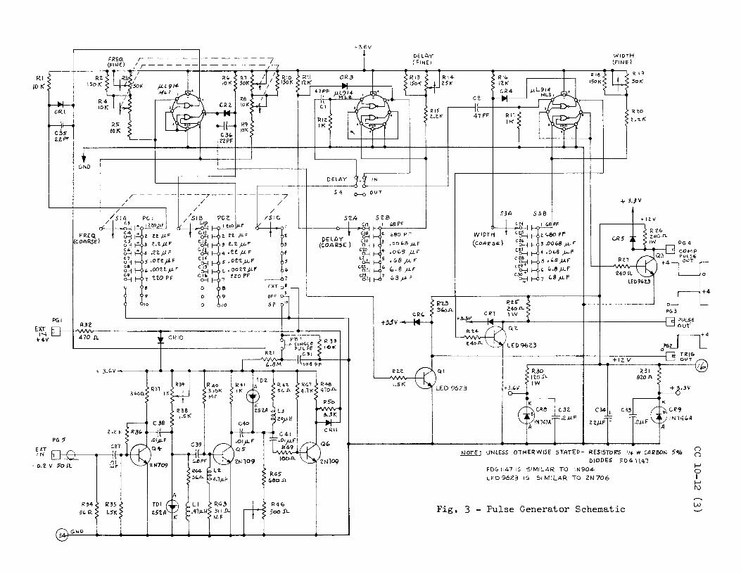
RI 10 I(
EXT IN
+4-V
CRI
C3S ZZ.Pf
PG :Y
RZ 15oK
GND
FREQ COARSE)
:14- G>IO
FREQ lFl~E)
r - ---- - - - - - - - - -7 ,1 ,-- - - -- -------,1
1<10 1501<
r- ____ T ___ ------7 /
/ /
/s1A / C3
f05 1.51(
PC I I a?DµF
t ZZ µF + 3 LZµ.F + 4 .nµF
~ ,OttjJ-F
' ,OO'lt fl- F 7 '1.tO PF
10
TDI tS'l.A
CRIO
A
K
/ /
0 0
PCZ
5 • Ot1._µ,F
b • OOZ1.JJ-F fZO PF
9 10
/ /SIC
+3 6V
Rll
DELAY (FINE!
l'Z.K,__ ______ --+-~
DELAY IN
54 0-0 OUT
S'lA- SUI c11 I '8 PF
CJ!.J L €>80 PF DtltlY C/9 3 • OD '-8 µ,F (COARSE) 0--I
C'Ul + ,0<08 J.LF 0--I CZI 5 ,(p8p.F o.!j G'&i '" ~.e µ.r c~ 7 i;,8 )>- F
CR'-+3.5V
CZ r----1f--+-~~.-----'
41 PF
S3A $38
cu WIDTH c~
(COAl<'S&:) c2' D--j
c.u
~~ c~
°+1
1?"1.3 f{Z/;"
3'°.n. 240.<l.. c 111 \W
WIDTH lFl'-'E)
R 19
501(
+ 3.JV
+ ltV -----1---CR5
+IZ V
C.32. 04 + C33 .2µF
Z Z.JJ.f -
PG 4 COMP
Q3 PUL5t +4-cr I
' ) '+4
o___r--1L PG3
NOTE: UNlESS OTHERWISE STATED - RESISTORS '/4 W CARBON 5% DIODES FDGl\41
0 0
I-' 0 I I-' I\)
FDG 1147 IS SIMILAR TO IN904 LED 96Z3 1S 51 Ml lAR TO ZN 706
Fig. 3 - Pulse Generator Schematic w

File No. CC 10-13 (l) D. A. Mack August 3, 1966
Lawrence Radiation Laboratory, University of California, Berkeley
COUNTING NOTE
NUCLEAR INSTRUMENT MODULE BIN
A number of pieces of laboratory and commercial equipment are constructed in Nuclear Instrument Modules (NIM). The 8-3/4" Nuclear Instrument Module Bin is designed to accept any 8-3/4" module and supply essentially all of its power requirements. Fig. l shows a front view of the bin.
Fig. l - Nuclear Instrument Module Bin
Table I lists the power capabilities of supplies presently in use at the Laboratory. Table II lists the buses that have been wired to bins in various stages of progress. Eventually all bins will be modified to correspond to the latest schedule (Type C). The actual voltages available will, of course, de-pend upon the power supplies t.hat are attached. At present one can depend upon ± 12 and ± 24 volts being available from any of the rear-mounting bin supplies. All other voltages must be supplied from either external or modular supplies.
REFERENCES :
l. TID-20893 (Rev.) Standard Nuclear Instrument Modules 2. UCRL-11702 Instrumentation Module System 3. Power Supply Specifications LRL-98-87
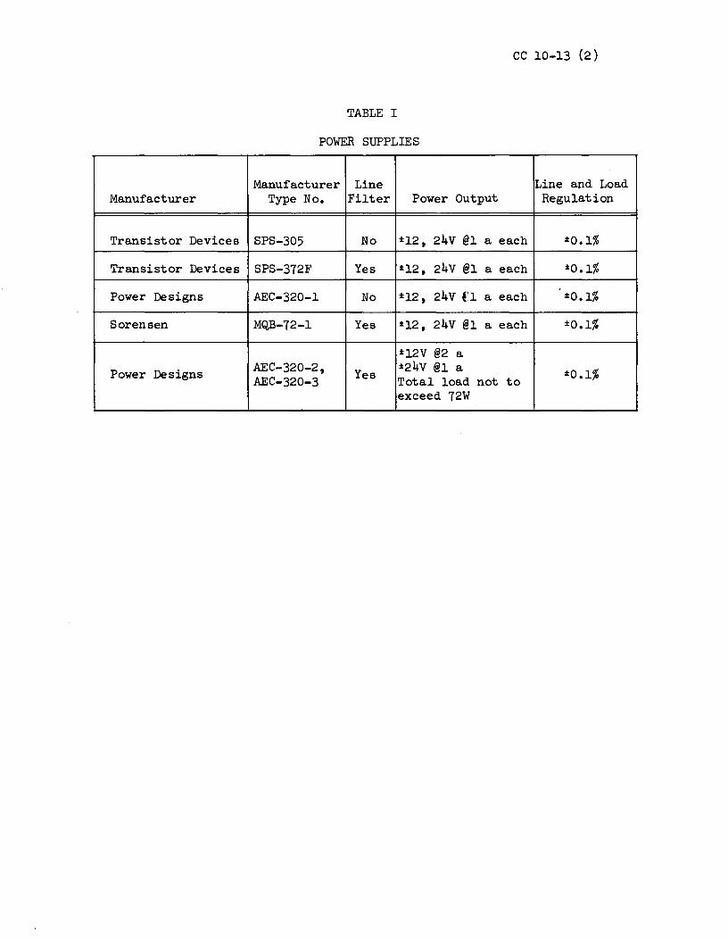
cc 10-13 (2)
TABLE I
POWER SUPPLIES
Manufacturer Line Line and Load Manufacturer Type No. Filter Power Output Regulation
Transistor Devices SPS-305 No ±12, 24V @l a each ±0.1%
Transistor Devices SPS-372F Yes ±12, 24V @l a each ±0.1%
Power Designs AEC-320-1 No ±12, 24V fl a each ±0.1%
Sorensen MQB-72-1 Yes ±12, 24V @l a each ±0.1%
±12V @2 a Power Designs AEC-320-2, Yes ±24V @l a ±0.1% AEC-320-3 Total load not to
exceed 72W
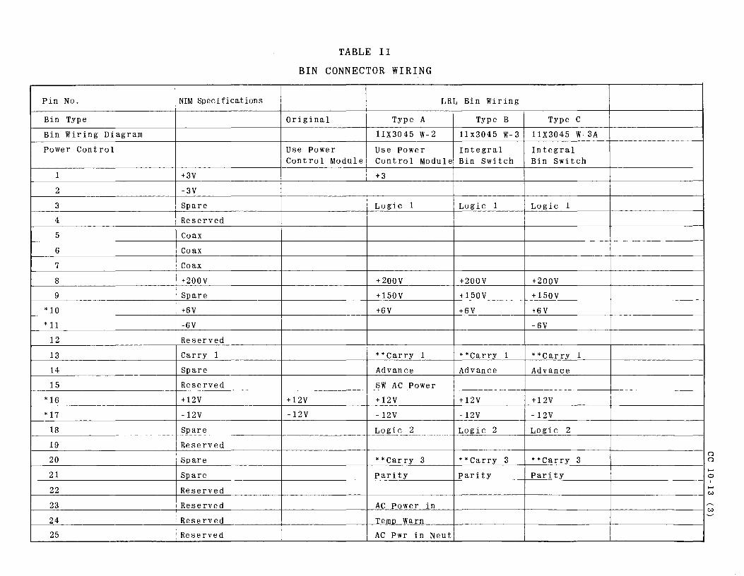
TABLE II
BIN CONNECTOR WIRING
Pin No. NIM Specifications LRL
Bin Type Original Type A
Bin Wiring Diagram l 1X30 45 W-2 Power Control Use Power Use Power
Control Module Control Module 1 +3V +3 2 -3V 3 Spare Logic 1 4 Reserved 5 Coax 6 Coax
7 Coax
8 +200V + 200V 9 Spare + 150V
*10 +6V +6V * 11 -6V
12 Reserved
13 Carry 1 **Carry 1 14 Spare Advance 15 Reserved SW AC Power
*16 +12V +12V +12V * 17 -12V -12V -12V
18 Spare Logic 2 19 Reserved 20 Spare **Carry 3 21 Spare Parity 22 Reserved 23 Reserved AC Power in 24 Reserved Temn Warn 25 Reserved AC Pwr in Neut
Bin Wiring
Type B 11 x3045 w- 3 Integral Bin Switch
Logic 1
+200V + 150V
+6V
**Carry 1 Advance
+12V
-12V Logic 2
**Carry 3 parity
Type c 11X3045 W-3A
Integral Bin Switch
Logic 1
+200V + 150V +6V -6V
**Carry 1
Advance
+12V -12V Logic 2
**Carry 3 Parity
...... 0
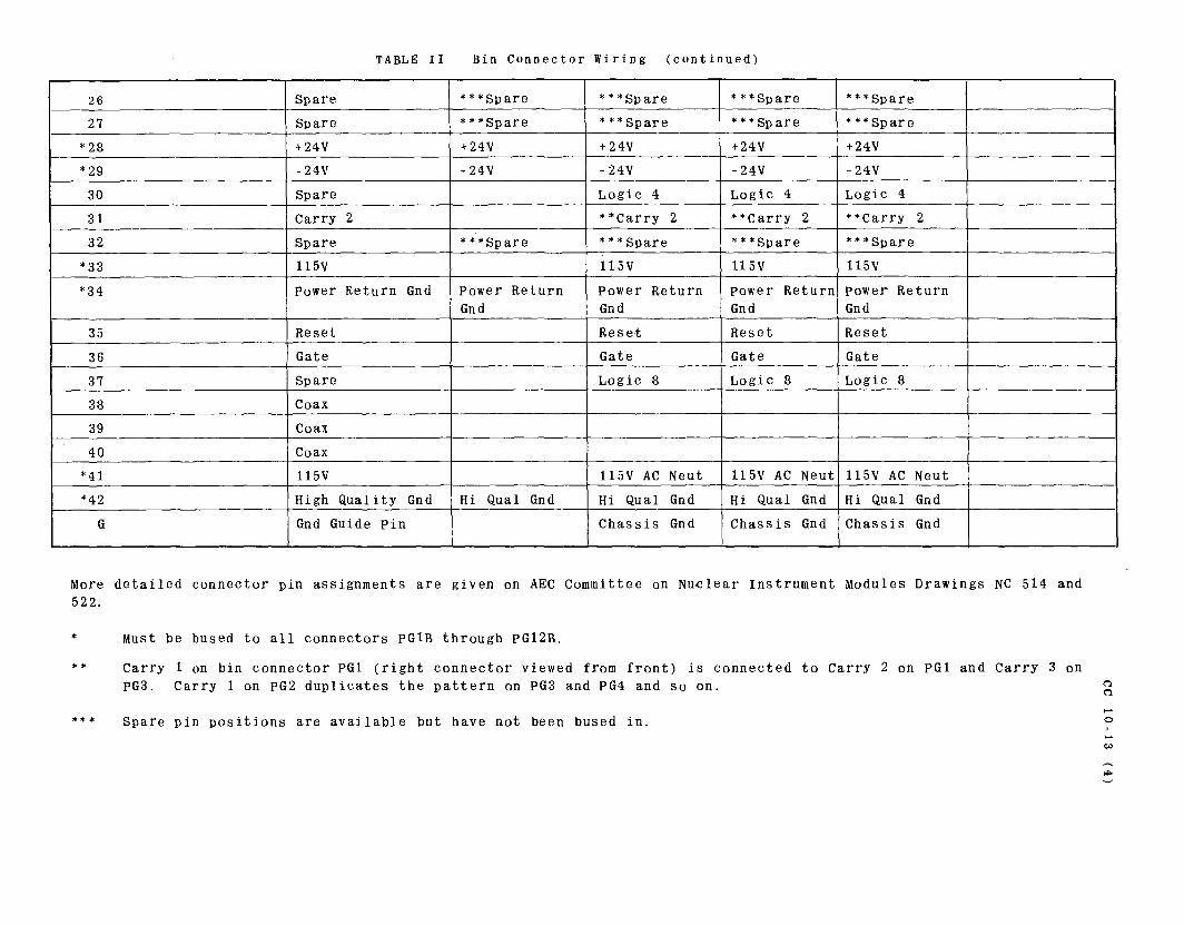
TABLE I I Bin Connector Wiring (continued)
26 Spare ***Spare ***Spare ***Spare ***Spare
27 Spare ***Spare ***Spare ***Spare ***Spare
* 28 +24V +24V +24V +24V +24V
* 29 -24V -24V -24V -24V -24V 30 Spare Logic 4 Logic 4 Logic 4
31 Carry 2 **Carry 2 **Carry 2 **Carry 2
32 Spare ***Spare ***Spare ***Spare ***Spare
*33 115V 115V 115V 115V
*34 Power Return Gnd Power Return Power Return rower Return Power Return Gnd Gnd Gnd Gnd
35 Reset Reset Reset Reset
36 Gate Gate Gate Gate
37 Spare Logic 8 Logic 8 Logic 8
38 Coax 39 Coax 40 Coax
*41 115V 115V AC Neut ll 5V AC Neut 115V AC Neut *42 High Quality Gnd Hi Qual Gnd Hi Qual Gnd Hi Qual Gnd Hi Qual Gnd
G Gnd Guide Pin Chassis Gnd Chassis Gnd Chassis Gnd
More detailed connector pin assignments are given on AEC Committee on Nu~lear Instrument Modules Drawings NC 514 and 522.
*
**
* * *
Must be bused to all connectors PGlB through PG12B.
Carry 1 on bin connector PGl (right connector viewed from front) is connected to Carry 2 on PGl and Carry 3 on PG3. Carry 1 on PG2 duplicates the pattern on PG3 and PG4 and so on.
Spare pin positions are available but have not been bused in. ..... 0
..... w
INDEX
Amplifiers
Nanosecond Pulse Amplifiers, Summary Evaluation of HP 460A and B Logic Amplifier 20 V Output Pulse Dual lns DCxlO Amplifier Spark Gap Trigger Amplifier
Attenuators ------Nanosecond
Cables
Coaxial, Pulse Response Coaxial, Physical Characteristics
Coincidence Systems
Dual 3-Channel, Model 3 Time-to-Height 4-Way "AND", l" INHIBIT 5-Way "OR" 5-Way Fanout 5-Way Fanout
Components for Amplitude Analysis
Summary, Pulse Height Analyzer Manufacturers' Data
Definitions
Logical Voltage Levels Performance Phototubes Pulse Terms
Del-a-gate
Delay Units
Delay Gate
Discriminators
Pulse Amplitude, Models 2 and 3 Radiation Laboratory Types
October 1, 1966
Section
CC l-2A cc 1-4 cc 1-6 cc 1-7 cc 1-8 CC 6-5A
CC 2-6B
CC 2-lB CC 2-2C
CC 3-lOA cc 3-15 cc 3-12 cc 3-13 cc 3-14 cc 3-16
cc 4-6
CC 5-9A cc 5-6 CC 5-8A cc 5-7 cc 10-5
cc 10-6
cc 3-11 CC 3-5B
Index (Continued) -2-
Electronic Circuits for Spark Chambers
Energy Distribution Box High Voltage Probe for Nanosecond Pulses Spark Gap Trigger Amplifier 15kv 20ma Spark Chamber Booster Supply
Gate and Delay Units
Delay Gate
Liggt Pulser
Corona
Photomul ti pliers
Corona Light Pulsers Gating, Electrical Light Pulses for Manufacturers' Data Measuring Techniques 6810 Class, Special Characteristics
Probe
High Voltage Probe for Nanosecond Pulses
Pulse He~ght Analyzers
Summary of Manufacturers' Data
Pulser
Corona Light Gated Light, for Photomultiplier Tube Testing Mercury Nanosecond Pulse Generators Pulse Generators
Scalers
Decade Scaler, Model 5 Decade Scaler and Readout System Operating Characteristics 10 MHz Decade Scaler
October 1, 1966
Section
cc 6-6 cc 6-7 CC 6-5A cc 6-8
cc 10-6
cc 8-30
cc 8-31
cc 8-31 cc 8-20 cc 8-30 CC 8-2C CC 8-3B CC 8-4A
cc 6-7
cc 4-6
cc 8-31 cc 10-4 cc 8-30 cc 10-1 cc 10-3 cc 10-8 cc 10-9
cc 9-9
CC 9-8A cc 9-10 CC 9-5C cc 9-11
Index (Continued) -3-
Scintillation Counters
Particle Detection by Scintillation Counters
Terminators
Nanosecond
Transformers 2 Pulse
Nanosecond
Waveform Generators & Power Supplies
Del-a-gate Delay Gate Gated Pulse Generator High-Voltage Power for Multiplier Phototubes Mercury Pulsers Nanosecond Pulse Generator Pulse Generators Pulse Generator Relay Driver Dual Delay Gate Pulse Generator Nuclear Instrument Module Bin
October 1, 1966
Section
CC 8-5A
CC 2-6B
CC 2-6B
cc 10-5 cc 10-6 cc 10-4 CC 10-lOA cc 10-1 cc 10-3 cc 10-8 cc 10-9 cc 10-7 cc 10-11 cc 10-12 cc 10-13


