Embed Size (px)
Citation preview

The present document has been developed within the 3rd Generation Partnership Project (3GPP TM) and may be further elaborated for the purposes of 3GPP.The present document has not been subject to any approval process by the 3GPP Organisational Partners and shall not be implemented.This Specification is provided for future development work within 3GPP only. The Organisational Partners accept no liability for any use of this Specification.Specifications and reports for implementation of the 3GPP TM system should be obtained via the 3GPP Organisational Partners' Publications Offices.
TS 25.102 V3.0.0 (1999-10)
Technical Specification
RP-99570
3rd Generation Partnership Project (3GPP);Technical Specification Group (TSG) RAN WG4;
UTRA (UE) TDD; Radio Transmission and Reception

3GPP
TS 25.102 V3.0.0 (1999-10)2
Reference<Workitem> (<Shortfilename>.PDF)
Keywords<keyword[, keyword]>
3GPP
Postal address
Office address
Individual copies of this deliverablecan be downloaded fromhttp://www.3gpp.org

3GPP
TS 25.102 V3.0.0 (1999-10)3
Contents
Intellectual Property Rights .......................................................................................................................... 6
Foreword...................................................................................................................................................... 6
1 Scope ................................................................................................................................................. 7
2 References.......................................................................................................................................... 7
3 Definitions, symbols and abbreviations ............................................................................................... 83.1 Definitions...................................................................................................................................................83.2 Symbols.......................................................................................................................................................83.3 Abbreviations ..............................................................................................................................................9
4 General ............................................................................................................................................ 104.1 Measurement uncertainty...........................................................................................................................10
5 Frequency bands and channel arrangement ........................................................................................ 115.1 General......................................................................................................................................................115.2 Frequency bands ........................................................................................................................................115.3 TX–RX frequency separation.....................................................................................................................115.4 Channel arrangement ................................................................................................................................115.4.1 Channel spacing...................................................................................................................................115.4.2 Channel raster......................................................................................................................................115.4.3 Channel number...................................................................................................................................11
6 Transmitter characteristics................................................................................................................ 136.1 General......................................................................................................................................................136.2 Transmit power .........................................................................................................................................136.2.1 User Equipment maximum output power..............................................................................................136.3 UE frequency stability................................................................................................................................136.4 Output power dynamics .............................................................................................................................146.4.1 Open loop power control ......................................................................................................................146.4.2 Inner loop power control ......................................................................................................................146.4.3 Power control steps...............................................................................................................................146.4.3.1 Minimum Requirements .................................................................................................................146.4.4 Power control cycles per second............................................................................................................146.4.4.1 Minimum Requirement ...................................................................................................................146.4.5 Minimum transmit output power ..........................................................................................................146.4.5.1 Minimum requirement ....................................................................................................................156.5 Transmit OFF power ................................................................................................................................156.5.1 Minimum Requirement ........................................................................................................................156.6 Output RF spectrum emissions..................................................................................................................156.6.1 Occupied bandwidth.............................................................................................................................156.6.2 Out of band emission............................................................................................................................156.6.2.1 Spectrum emission mask.................................................................................................................156.6.2.1.1 Minimum Requirement..............................................................................................................156.6.2.2 Adjacent Channel Leakage power Ratio (ACLR) ............................................................................166.6.2.2.1 Minimum requirement...............................................................................................................166.6.3 Spurious emissions...............................................................................................................................166.6.3.1 Minimum Requirement ..................................................................................................................166.7 Transmit intermodulation ..........................................................................................................................176.7.1 Minimum requirement .........................................................................................................................176.8 Transmit Modulation.................................................................................................................................176.8.1 Transmit pulse shape filter ...................................................................................................................176.8.2 Modulation Accuracy ...........................................................................................................................176.8.2.1 Minimum Requirement ...................................................................................................................176.8.3 Peak Code Domain Error......................................................................................................................176.8.3.1 Minimum Requirement ...................................................................................................................18

3GPP
TS 25.102 V3.0.0 (1999-10)4
7 Receiver characteristics .................................................................................................................... 197.1 General......................................................................................................................................................197.2 Diversity characteristics.............................................................................................................................197.3 Reference sensitivity level..........................................................................................................................197.3.1 Minimum Requirements.......................................................................................................................197.4 Maximum input level.................................................................................................................................197.4.1 Minimum Requirements.......................................................................................................................197.5 Adjacent Channel Selectivity (ACS) ..........................................................................................................207.5.1 Minimum Requirement ........................................................................................................................207.6 Blocking characteristics .............................................................................................................................207.6.1 Minimum Requirement ........................................................................................................................207.7 Spurious response ......................................................................................................................................217.7.1 Minimum Requirement ........................................................................................................................217.8 Intermodulation characteristics ..................................................................................................................217.8.1 Minimum Requirements.......................................................................................................................227.9 Spurious emissions ....................................................................................................................................227.9.1 Minimum Requirement ........................................................................................................................22
8 Performance requirement .................................................................................................................. 238.1 General......................................................................................................................................................238.2 Demodulation in static propagation conditions...........................................................................................238.2.1 Demodulation of DCH..........................................................................................................................238.2.1.1 Minimum requirement ....................................................................................................................238.2.2 Demodulation of BCH..........................................................................................................................238.2.2.1 Minimum requirement ....................................................................................................................248.3 Demodulation of DCH in multipath fading conditions ...............................................................................248.3.1 Multipath fading Case 1 .......................................................................................................................248.3.1.1 Minimum requirement ....................................................................................................................248.3.2 Multipath fading Case 2 .......................................................................................................................248.3.2.1 Minimum requirement ....................................................................................................................248.3.3 Multipath fading Case 3 .......................................................................................................................248.3.3.1 Minimum requirement ....................................................................................................................258.4 Demodulation of BCH in multipath fading conditions................................................................................258.4.1 Multipath fading Case 1 .......................................................................................................................258.4.1.1 Minimum requirement ....................................................................................................................258.5 Rx synchronisation characterisitics ............................................................................................................268.5.1 Synchronization Performance...............................................................................................................268.5.1.1 Search of other Cells .......................................................................................................................268.5.1.1.1 Minimum requirements .............................................................................................................268.5.2 Inter-Frequency Handover. ...................................................................................................................268.5.2.1 Minimum Requirements .................................................................................................................268.6 Timing requirements .................................................................................................................................268.6.1 Synchronization ...................................................................................................................................268.6.1.1 Minimum Requirements .................................................................................................................26
Annex A (normative): Measurement channels............................................................................................. 27A.1 General......................................................................................................................................................27A.2 Reference measurement channel ................................................................................................................27A.2.1 UL reference measurement channel (12.2 kbps)....................................................................................27A.2.2 DL reference measurement channel (12.2 kbps) ...................................................................................28A.2.3 DL reference measurement channel (64 kbps) ......................................................................................29A.2.4 DL reference measurement channel (144 kbps) ....................................................................................30A.2.5 DL reference measurement channel (384 kbps) ....................................................................................31A.2.6 BCH reference measurement channel ...................................................................................................32
Annex B (normative): Propagation conditions ............................................................................................. 33B.2 Static propagation condition ......................................................................................................................33B.2 Multi-path fading propagation conditions ..................................................................................................33
Annex C (normative): Environmental conditions.......................................................................................... 34C.1 General......................................................................................................................................................34

3GPP
TS 25.102 V3.0.0 (1999-10)5
C.2 Environmental requirements for the UE.....................................................................................................34C.2.1 Temperature.........................................................................................................................................34C.2.2 Voltage ...............................................................................................................................................34C.2.3 Vibration.............................................................................................................................................35
Annex D (informative): Open items............................................................................................................. 36
ANNEX E (INFORMATIVE): Terminal Capabilities (TDD)...................................................................... 37E.1 Baseline Implementation Capabilities ........................................................................................................37E.2 Service Implementation Capabilities ..........................................................................................................37
History....................................................................................................................................................... 38

3GPP
TS 25.102 V3.0.0 (1999-10)6
Intellectual Property RightsIPRs essential or potentially essential to the present document may have been declared to ETSI. The informationpertaining to these essential IPRs, if any, is publicly available for ETSI members and non-members, and can befound in ETR 314: "Intellectual Property Rights (IPRs); Essential, or potentially Essential, IPRs notified to ETSI inrespect of ETSI standards", which is available free of charge from the ETSI Secretariat. Latest updates are availableon the ETSI Web server (http://www.etsi.fr/ipr).
Pursuant to the ETSI Interim IPR Policy, no investigation, including IPR searches, has been carried out by ETSI. Noguarantee can be given as to the existence of other IPRs not referenced in ETR 314 (or the updates onhttp://www.etsi.fr/ipr) which are, or may be, or may become, essential to the present document.
ForewordThis Technical Specification has been produced by the 3GPP.
The contents of the present document are subject to continuing work within the TSG and may change followingformal TSG approval. Should the TSG modify the contents of this TS, it will be re-released by the TSG with anidentifying change of release date and an increase in version number as follows:
Version 3.y.z
where:
x the first digit:
1 presented to TSG for information;
2 presented to TSG for approval;
3 Indicates TSG approved document under change control.
y the second digit is incremented for all changes of substance, i.e. technical enhancements, corrections,updates, etc.
z the third digit is incremented when editorial only changes have been incorporated in the specification;

3GPP
TS 25.102 V3.0.0 (1999-10)7
1 ScopeThis document establishes the minimum RF characteristics of the TDD mode of UTRA for the User Equipment (UE).
2 ReferencesThe following documents contain provisions, which, through reference in this text, constitute provisions of the presentdocument.
• References are either specific (identified by date of publication, edition number, version number, etc.) ornon-specific.
• For a specific reference, subsequent revisions do not apply.
• For a non-specific reference, subsequent revisions do apply.
• A non-specific reference to an ETS shall also be taken to refer to later versions published as an EN with thesame number.

3GPP
TS 25.102 V3.0.0 (1999-10)8
3 Definitions, symbols and abbreviations
3.1 DefinitionsFor the purposes of the present document, the following definitions apply:
Power Setting The value of the control signal, which determines the desired transmitter, outputPower. Typically, the power setting would be altered in response to power controlcommands
Maximum Power Setting The highest value of the Power control setting which can be used.Maximum output Power This refers to the measure of power when averaged over the transmit timeslot at the
maximum power setting.Peak Power The instantaneous power of the RF envelope which is not expected to be exceeded
for [99.9%] of the timeMaximum peak power The peak power observed when operating at a given maximum output power.Average transmit power The average transmitter output power obtained over any specified time interval,
including periods with no transmission.<Editors: This definition would be relevant when considering realistic deploymentscenarios where the power control setting may vary. >
Maximum average power The average transmitter output power obtained over any specified time interval,including periods with no transmission, when the transmit time slots are at themaximum power setting. <Editors: The average power at the maximum power setting would also beconsistent with defining a long term average power>
Received Signal CodePower (RSCP)
Given only signal power is received, the average power of the received signal afterdespreading and combining.
Interference Signal CodePower (ISCP)
Given only interference power is received, the average power of the received signalafter despreading to the code and combining. Equivalent to the RSCP value butnow only interference is received instead of signal
3.2 SymbolsFor the purposes of the present document, the following symbols apply:
<symbol> <Explanation>

3GPP
TS 25.102 V3.0.0 (1999-10)9
3.3 AbbreviationsFor the purposes of the present document, the following abbreviations apply:
ACIR Adjacent Channel Interference RatioACLR Adjacent Channel Leakage power RatioACS Adjacent Channel SelectivityBS Base StationCW Continuous wave (unmodulated signal)DL Down link (forward link)DPCH Dedicated physical channelDPCH_Ec Average energy per PN chip for DPCH
orI
DPCH_Ec The ratio of the average energy per PN chip of the DPCH to the total transmit powerspectral density of the forward link at the BS antenna connector
EIRP Effective Isotropic Radiated PowerFDD Frequency Division DuplexingFER Frame Error RateIor The total transmit power spectral density of the Forward link at the BS antenna
connector
orI The received power spectral density of the Forward link as measured at the UEantenna connector
PPM Parts Per MillionRSSI Received Signal Strength IndicatorSIR Signal to Interference ratioTDD Time Division DuplexingTPC Transmit Power ControlUE User EquipmentUL Up link (reverse link)UTRA UMTS Terrestrial Radio Access

3GPP
TS 25.102 V3.0.0 (1999-10)10
4 General
4.1 Measurement uncertaintyThe requirements given in these specifications are absolute. Compliance with these requirements are determined bycomparing the measured values with the specified limits, without making allowance for measurement uncertainty.

3GPP
TS 25.102 V3.0.0 (1999-10)11
5 Frequency bands and channel arrangement
5.1 GeneralThe information presented in this section is based on a chip rate of 3.84 Mcps.
Note
1. Other chip rates may be considered in future releases.
5.2 Frequency bandsUTRA/TDD is designed to operate in the following bands;
a) 1900 – 1920 MHz: Uplink and downlink transmission2010 – 2025 MHz Uplink and downlink transmission
b)* 1850 – 1910 MHz: Uplink and downlink transmission 1930 – 1990 MHz: Uplink and downlink transmission
Note: Appropriate adjustment is required for the parameters in the specified band
c)* 1910 – 1930 MHz: Uplink and downlink transmissionNote: Appropriate adjustment is required for the parameters in the specified band
* Used in ITU Region 2
Additional allocations in ITU region 2 are FFS.
Deployment in other frequency bands is not precluded.
The co-existence of TDD and FDD in the same bands is still under study in WG4.
5.3 TX–RX frequency separationNo TX-RX frequency separation is required as Time Division Duplex (TDD) is employed. Each TDMA frame consistsof 15 timeslots where each timeslot can be allocated to either transmit or receive.
5.4 Channel arrangement
5.4.1 Channel spacing
The nominal channel spacing is 5 MHz, but this can be adjusted to optimise performance in a particular deploymentscenario.
5.4.2 Channel raster
The channel raster is 200 kHz, which means that the carrier frequency must be a multiple of 200 kHz.
5.4.3 Channel number
The carrier frequency is designated by the UTRA absolute radio frequency channel number (UARFCN). The value ofthe UARFCN in the IMT2000 band is defined as follows:

3GPP
TS 25.102 V3.0.0 (1999-10)12
Lower IMT 2000 band:
Nt = 5 ∗ ( F – 1885.2) 1885.2 ≤ F ≤ 2024.8 where F is the carrier frequency in MHz

3GPP
TS 25.102 V3.0.0 (1999-10)13
6 Transmitter characteristics
6.1 GeneralUnless detailed the transmitter characteristic are specified at the antenna connector of the UE. For UE with integralantenna only, a reference antenna with a gain of 0 dBi is assumed. Transmitter characteristics for UE(s) with multipleantennas/antenna connectors are FFS.
The UE antenna performance has a significant impact on system performance and minimum requirements on theantenna efficiency are therefore intended to be included in future versions of this specification. It is recognised thatdifferent requirements and test methods are likely to be required for the different types of UE.
All the parameters in section 6 are defined using the UL reference measurement channel (12.2 kbps) specified inAnnex A.2.1.
6.2 Transmit power
6.2.1 User Equipment maximum output power
The following Power Classes define the maximum output power;
Table 6.1: UE power classes
Power Class Maximum output power Tolerance
1 +30 dBm +1dB /-3dB
2 +24 dBm +1dB /-3dB
3 +21 dBm +2dB /-2dB]
4 +10 dBm +4dB /-4dB
Note1. The maximum output power refers to the measure of power when averaged over the useful part of the transmit
timeslot at the maximum power control setting.2. For multi-code operation the maximum output power will be reduced by the difference of peak to average ratio
between single and multi-code transmission. The error of the maximum average power is below the prescribedvalue even at the multi-code transmission mode <new text is required to clarify this sentence>
3. Power class 4 is envisaged for licensed exempt operation.4. For UE using directive antennas for transmission, a class dependent limit will be placed on the maximum EIRP
(Equivalent Isotropic Radiated Power)..
6.3 UE frequency stability
The UE modulated carrier frequency shall be accurate to within ±0.1 PPM compared to carrier frequency receivedfrom the BS. These signals will have an apparent error due to BS frequency error and Doppler shift. In the later case,signals from the BS must be averaged over sufficient time that errors due to noise or interference are allowed forwithin the above ±0.1PPM figure.
Table 6.2: Frequency stability
AFC Frequency stability
ON within ± 0.1 PPM

3GPP
TS 25.102 V3.0.0 (1999-10)14
6.4 Output power dynamicsPower control is used to limit the interference level.
6.4.1 Open loop power control
Open loop power control is the ability of the UE transmitter to sets its output power to a specified value. For the TDDmode the reciprocity of the channel allows accurate estimation of the required open loop transmit power.
The UE open loop power control error shall be less than +/-9dB under normal conditions and +/- 12dB under extremeconditions.
6.4.2 Inner loop power control
Inner loop power control is the ability of the UE transmitter to adjust its output power in accordance to the TPCsymbols received in the downlink.
6.4.3 Power control steps
The power control step is the step change in the UL transmitter output power in response to a TPC message. A set ofpower control steps is defined.
6.4.3.1 Minimum Requirements
The mobile station transmitter shall have the capability of setting power with a step of 1, 2 and 3dB. tolerance of thetransmitter output power and the greatest average rate of change in mean power due to the power control step shall bewithin the range shown in Table 6.3.
Table 6.3: Power control step size tolerance
Range of average rate of change inmean power per 10 steps
Step size Tolerance
minimum maximum
1dB +/-0.5dB +/-8dB +/-12dB
2dB +/-1dB +/-16dB +/-24dB
3dB +/-1.5dB +/-24dB +/-36dB
6.4.4 Power control cycles per second
The maximum and minimum rate of change for the UL transmitter power control step.
6.4.4.1 Minimum Requirement
The rate of change for the UL transmitter power control step is a s follows: 100 – 800 Hz.
The minimum rate of 100 Hz is to ensure that every frame is power controlled. The maximum rate may differ for openand closed loop power control due to the used frame configuration.
6.4.5 Minimum transmit output power
The minimum controlled output power of the UE is when the power control setting is set to a minimum value. This iswhen both the closed loop and open loop power control indicates a minimum transmit output power is required.

3GPP
TS 25.102 V3.0.0 (1999-10)15
6.4.5.1 Minimum requirement
The minimum transmit power shall be better than–44 dBm measured with a filter that has a root-raised cosine (RRC)filter response with a roll-off-factor α = 0.22 and a bandwidth equal to the chip rate.
6.5 Transmit OFF power
The transmit OFF power state is when the UE does not transmit. This parameter is defined as the maximumoutput transmit power within the channel bandwidth when the transmitter is OFF.
6.5.1 Minimum Requirement
The requirement for transmit OFF power shall be better than −65 dBm measured with a filter that has a Root-Raised Cosine (RRC) filter response with a roll off α=0.22 and a bandwidth equal to the chip rate.
6.6 Output RF spectrum emissions
6.6.1 Occupied bandwidth
Occupied bandwidth is a measure of the bandwidth containing 99% of the total integrated power of the transmittedspectrum, centred on the assigned channel frequency. The occupied channel bandwidth shall be less than 5 MHz basedon a chip rate of 3.84 Mcps.
6.6.2 Out of band emission
Out of band emissions are unwanted emissions immediately outside the nominal channel resulting from themodulation process and non-linearity in the transmitter but excluding spurious emissions. This out of band emissionlimit is specified in terms of a spectrum emission mask and adjacent channel power ratio.
6.6.2.1 Spectrum emission mask
The spectrum emission mask of the UE applies to frequencies, which are between 2.5 and 12.5MHz from acarrier frequency. The out of channel emission is specified relative to the UE output power in measured in a 3.84MHz bandwidth.
6.6.2.1.1 Minimum Requirement
The power of the 21dBm power class 3 UE emission shall not exceed the levels specified in table 6.4.
Table 6.4 : Spectrum Emission Mask Requirement
Frequency offset from carrier �f Minimum requirement Measurement bandwidth
2.5 - 3.5 MHz -35 -15*(∆f – 2.5) dBc 30 kHz *
3.5 - 7.5 MHz -35- 1*(∆f-3.5) dBc 1 MHz *
7.5 - 8.5 MHz -39 - 10*(∆f – 7.5) dBc 1 MHz *
8.5 - 12.5 MHz -49 dBc 1 MHz *
Note
1. The first and last measurement position with a 30 kHz filter is 2.515 MHz and 3.485 MHz
2. The first and last measurement position with a 1 MHz filter is 4 MHz and 12 MHz

3GPP
TS 25.102 V3.0.0 (1999-10)16
3. The lower limit shall be –50dBm/3.84 MHz or which ever is the higher
6.6.2.2 Adjacent Channel Leakage power Ratio (ACLR)
Adjacent Channel Leakage power Ratio (ACLR) is the ratio of the transmitted power to the power measured after areceive filter in the adjacent channels(s). Both the transmitted power and the received power are measured with a filterresponse that has a Root-Raised Cosine (RRC) filter response with roll-off α = 0.22 and a bandwidth equal to the chiprate.
6.6.2.2.1 Minimum requirement
The ACLR shall be better than the value specified in Table 6.5.
Table 6.5 :UE ACLR
Power Class UE channel ACLR limit
3 ± 5 MHz -33 dB or –50 dBm which ever is higher
3 ± 10 MHz -43 dB or –50 dBm which ever is higher
Note
1. The ACLR due to switching transients shall not exceed the limits in the above table.
6.6.3 Spurious emissions
Spurious emissions are emissions which are caused by unwanted transmitter effects such as harmonics emission,parasitic emission, intermodulation products and frequency conversion products, but exclude out of band emissions.
The frequency boundary and the detailed transitions of the limits between the requirement for out band emissions andspectrum emissions are based on ITU-R Recommendations SM.329.
6.6.3.1 Minimum Requirement
These requirements are only applicable for frequencies which are greater than 12.5 MHz away from the UE centercarrier frequency.
Table 6.6a : General Spurious emissions requirements
Frequency Bandwidth Resolution Bandwidth Minimum requirement
9 kHz ≤ f < 150 kHz 1 kHz -36 dBm150 kHz ≤ f < 30 MHz 10 kHz -36 dBm
30 MHz ≤ f < 1000 MHz 100 kHz -36 dBm1 GHz ≤ f < 12.75 GHz 1 MHz -30 dBm
Table 6.6b : Additional Spurious emissions requirements
Frequency Bandwidth Resolution Bandwidth Minimum requirement
925 MHz ≤ f ≤ 935 MHz 100 KHz -67 dBm*935 MHz < f ≤ 960 MHz 100 KHz -79 dBm*
1805 MHz ≤ f ≤ 1880 MHz 100 KHz -71 dBm*
Note
* The measurements are made on frequencies which are integer multiples of 200 kHz. As exceptions, up to fivemeasurements with a level up to the applicable requirements defined in Table 6.6b are permitted for each UARFCNused in the measurement.

3GPP
TS 25.102 V3.0.0 (1999-10)17
6.7 Transmit intermodulationThe transmit intermodulation performance is a measure of the capability of the transmitter to inhibit the generation ofsignals in its non linear elements caused by presence of the wanted signal and an interfering signal reaching thetransmitter via the antenna.
6.7.1 Minimum requirement
User Equipment(s) transmitting in close vicinity of each other can produce intermodulation products, which can fallinto the UE, or BS receive band as an unwanted interfering signal. The UE intermodulation attenuation is defined bythe ratio of the output power of the wanted signal to the output power of the intermodulation product when aninterfering CW signal is added at a level below the wanted signal. Both the wanted signal power and theintermodulation product power are measured with a filter response that is root-raised cosine (RRC) with roll-offα=0.22 and with a bandwidth equal to the chip rate.The requirement of transmitting intermodulation for carrier spacing 5 MHz is prescribed in the Table below.
Table 6.7 : Transmit Intermodulation
Interference Signal Frequency Offset 5MHz 10MHz
Interference Signal Level -40 dBc
Minimum Requirement -31dBc -41dBc
Note: This requirement is applicable to the 21 dBm power class 3 UE.
6.8 Transmit Modulation
6.8.1 Transmit pulse shape filter
The transmit pulse-shaping filter is a root-raised cosine (RRC) with roll-off α =0.22 in the frequency domain. Theimpulse response of the chip impulse filter RC0(t) is
( )( ) ( )
−
++
−
=20
41
1cos41sin
CC
CCC
T
t
T
t
T
t
T
t
T
t
tRC
απ
απααπ
Where the roll-off factor α =0.22 and the chip duration: schiprate
TC µ26042.01
≈=
6.8.2 Modulation Accuracy
The modulation accuracy is a measure of the difference between the measured waveform and the theoretical modulatedwaveform (the error vector). It is the square root of the ratio of the mean error vector power to the mean referencesignal power expressed as a %. The measurement interval is one timeslot.
6.8.2.1 Minimum Requirement
The modulation accuracy shall not exceed 17.5 %.
6.8.3 Peak Code Domain Error
This specification is applicable for multi-code transmission only.

3GPP
TS 25.102 V3.0.0 (1999-10)18
The code domain error is computed by projecting the error vector power onto the code domain at the maximumspreading factor. The error power for each code is defined as the ratio to the mean power of the reference waveformexpressed in dB. And the Peak Code Domain Error is defined as the maximum value for Code Domain Error. Themeasurement interval is one timeslot.
6.8.3.1 Minimum Requirement
The peak code domain error shall not exceed [ ] dB.

3GPP
TS 25.102 V3.0.0 (1999-10)19
7 Receiver characteristics
7.1 GeneralUnless detailed the receiver characteristic are specified at the antenna connector of the UE. For UE with an integralantenna only, a reference antenna with a gain of 0 dBi is assumed. UE with an integral antenna may be taken intoaccount by converting these power levels into field strength requirements, assuming a 0 dBi gain antenna. Receivercharacteristics for UE(s) with multiple antennas/antenna connectors are FFS.
The UE antenna performance has a significant impact on system performance, and minimum requirements on theantenna efficiency are therefore intended to be included in future versions of this specification. It is recognised thatdifferent requirements and test methods are likely to be required for the different types of UE.
All the parameters in Section 7 are defined using the DL reference measurement channel specified in AnnexA.2.2.
7.2 Diversity characteristicsA suitable receiver structure using coherent reception in both channel impulse response estimation, and code trackingprocedures is assumed. Three forms of diversity are considered to be available in UTRA/TDD:
Table 6, Diversity characteristics for UTRA/TDD.
Table 7.1 : Diversity characteristics for UTRA/FDD
Time diversity Channel coding and interleaving in both up link and down link
Multi-pathdiversity
Rake receiver or other suitable receiver structure with maximumcombining. Additional processing elements can increase the delay-spreadperformance due to increased capture of signal energy.
Antenna diversity Antenna diversity with maximum ratio combing in the base station andoptionally in the mobile stations. Possibility for downlink transmitdiversity in the base station.
7.3 Reference sensitivity levelThe reference sensitivity is the minimum receiver input power measured at the antenna port at which the BIT ErrorRate BER does not exceed a specific value.
7.3.1 Minimum Requirements
Table 7.2 : Reference sensitivity level
Data rate UE reference sensitivity level (dBm) FER/BER
12.2 kbps -105 dBm BER shall not exceed 0.001
7.4 Maximum input levelThis is defined as the maximum receiver input power at the UE antenna port which does not degrade the specifiedBER performance.
7.4.1 Minimum Requirements
The BER shall not exceed 0.001 for the parameters specified in Table 7.3.

3GPP
TS 25.102 V3.0.0 (1999-10)20
Table 7.3: Maximum input level
Parameter Level Unit
orI
DPCH_Ec -7 dB
orI-25 dBm/3.84 MHz
7.5 Adjacent Channel Selectivity (ACS)Adjacent Channel Selectivity is a measure of a receiver’s ability to receive a wanted signal at its assigned channelfrequency in the presence of adjacent channel signal at a given frequency offset from the centre frequency of theassigned channel. ACS is the ratio of the receive filter attenuation on the assigned channel frequency to the receiverfilter attenuation on the adjacent channel(s).
7.5.1 Minimum Requirement
The BER shall not exceed 0.001 for the parameters specified in Table 7.4.
Table 7.4: Adjacent Channel Selectivity
Power Class ACS Units3 [33] dB
Parameter Level Unit
Data rate 12.2 kbps
Wanted signal [ ] dBm
Interfering signal [ ] dBm
Fuw (Modulated) 5 MHz
7.6 Blocking characteristics The blocking characteristics is a measure of the receiver ability to receive a wanted signal at is assigned channelfrequency in the presence of an unwanted interferer on frequencies other than those of the spurious response or theadjacent channels. The blocking performance shall apply at all frequencies except those at which a spurious responseoccur.
7.6.1 Minimum Requirement
The BER shall not exceed 0.001 for the parameters specified in table 7.5 and table 7.6. For table 13 up to 24exceptions are allowed for spurious response frequencies in each assigned frequency channel when measured using a1MHz step size.
Table 7.5: In-band blocking

3GPP
TS 25.102 V3.0.0 (1999-10)21
Parameter Offset Offset Unit
Wanted SignalLevel
<REFSENS> + 3 dB <REFSENS> + 3 dB dBm/3.84 MHz
Unwanted SignalLevel (modulated)
-56 -44 dBm/3.84 MHz
Blocking offset 10<|f-fo|<15 |f-fo|≥15 MHz
Table 7.6: Out of band blocking
Parameter Band 1 Band 2 Band 3 Unit
Wanted SignalLevel
<REFSENS> + 3 dB <REFSENS> + 3 dB <REFSENS> + 3 dBdBm/3.84 MHz
UnwantedSignal Level(CW)
-44 -30 -15 dBm
Blocking offset 1840 <f <1885
1935 <f <1995
2040 <f <2095
1815 <f <1840
2095 <f <2120
1< f <1815
2120< f <12750
MHz
Note: On frequency regions 1885 <f< 1900 MHz, 1920 <f< 1935 MHz, 1995 <f< 2010 MHz and2025<f< 2040 MHz, the appropriate in-band blocking or adjacent channel selectivity in section 7.5.1 shall beapplied.
7.7 Spurious responseSpurious response is a measure of the receiver’s ability to receive a wanted signal on its assigned channel frequencywithout exceeding a given degradation due to the presence of an unwanted CW interfering signal at any otherfrequency at which a response is obtained i.e. for which the blocking limit is not met.
7.7.1 Minimum Requirement
The BER shall not exceed 0.001 for the parameters specified in Table 7.7.
Table 7.7: Spurious Response
Parameter Level Unit
Wanted Signal Level <REFSENS> + 3 dB dBm/3.84 MHz
Unwanted SignalLevel (CW)
-44 dBm
Fcw Spurious responsefrequencies
MHz
7.8 Intermodulation characteristics Third and higher order mixing of the two interfering RF signals can produce an interfering signal in the band of thedesired channel. Intermodulation response rejection is a measure of the capability of the receiver to receiver a wantedsignal on its assigned channel frequency in the presence of two or more interfering signals which have a specificfrequency relationship to the wanted signal.

3GPP
TS 25.102 V3.0.0 (1999-10)22
7.8.1 Minimum Requirements
The BER shall not exceed 0.001 for the parameters specified in table 7.8.
Table 7.8: Receive intermodulation characteristics
Parameter Level Unit
Wanted Signal Level <REFSENS> + 3 dB dBm/3.84 MHz
Iouw1 -46 dBm
Iouw2 -46 dBm/3.84 MHz
Fuw1 (CW) 10 MHz
Fuw2 (Modulated) 20 MHz
7.9 Spurious emissionsThe Spurious Emissions Power is the power of emissions generated or amplified in a receiver that appear at the UEantenna connector.
7.9.1 Minimum Requirement
The spurious emission shall be:
1. Less than [-60dBm/ 3.84MHz] at the mobile station antenna connector, for frequencies within the UE receiveband.
2. Less than [-57dBm/100kHz] at the mobile station antenna connector, for frequencies band from 9kHz to 1GHz.
3. Less than [-47dBm/100kHz] at the mobile station antenna connector, for frequencies band from 1GHz to12.75GHz.

3GPP
TS 25.102 V3.0.0 (1999-10)23
8 Performance requirement
8.1 GeneralThe performance requirements for the UE in this section are specified for the measurement channels specified inAnnex A and the propagation condition specified in Annex B.
Table 8.1: Summary of UE performance targets
Static Multi-pathCase 1
Multi-pathCase 2
Multi-pathCase 3
TestChs.
InformationData Rate
Performance metric
12.2 kbps
64 kbps
144 kbps
384 kbps
DCH
2048 kbps
BCH
8.2 Demodulation in static propagation conditions
8.2.1 Demodulation of DCH
The performance requirement of DCH in static propagation conditions is determined by the maximum Block ErrorRate (BLER ). The BLER is specified for each individual data rate of the DCH.
8.2.1.1 Minimum requirement
The BLER should not exceed the limit for the Eb/N0 specified in Table 8.2.
Table 8.2: Performance requirements in AWGN channel.
Measurement channel
12.2 kbps
64 kbps
144 kbps
384 kbps
2048 kbps
8.2.2 Demodulation of BCH

3GPP
TS 25.102 V3.0.0 (1999-10)24
8.2.2.1 Minimum requirement
8.3 Demodulation of DCH in multipath fading conditions
8.3.1 Multipath fading Case 1
The performance requirement of DCH is determined by the maximum Block Error Rate (BLER ). The BLER isspecified for each individual data rate of the DCH.
8.3.1.1 Minimum requirement
The BLER should not exceed the limit for the Eb/N0 specified in Table 8.3.
Table 8.3: Performance requirements in multipath Case 1 channel.
Measurement channel
12.2 kbps
64 kbps
144 kbps
384 kbps
2048 kbps
8.3.2 Multipath fading Case 2
The performance requirement of DCH is determined by the maximum Block Error Rate (BLER ). The BLER isspecified for each individual data rate of the DCH.
8.3.2.1 Minimum requirement
The BLER should not exceed the limit for the Eb/N0 specified in Table 8.4.
Table 8.4: Performance requirements in multipath Case 2 channel.
Measurement channel
12.2 kbps
64 kbps
144 kbps
384 kbps
8.3.3 Multipath fading Case 3
The performance requirement of DCH is determined by the maximum Block Error Rate (BLER ). The BLER isspecified for each individual data rate of the DCH.

3GPP
TS 25.102 V3.0.0 (1999-10)25
8.3.3.1 Minimum requirement
The BLER should not exceed the limit for the Eb/N0 specified in Table 8.5.
Table 8.5: Performance requirements in multipath Case 3 channel.
Measurement channel
12.2 kbps
64 kbps
144 kbps
384 kbps
8.4 Demodulation of BCH in multipath fading conditions
8.4.1 Multipath fading Case 1
8.4.1.1 Minimum requirement

3GPP
TS 25.102 V3.0.0 (1999-10)26
8.5 Rx synchronisation characterisitics
8.5.1 Synchronization Performance
8.5.1.1 Search of other Cells
Search of other cells test is used to check whether the UE correctly searches and measures other BS(s) during thespecified operation.
8.5.1.1.1 Minimum requirements
TBD
8.5.2 Inter-Frequency Handover.
The UE has to have the ability to make an Inter-frequency handover. This type of handover can happen within a BS orbetween two BS(s). Currently [ARIB Vol. 3] does not define requirements for Inter-frequency handover. <This item isffs>
8.5.2.1 Minimum Requirements
TBD
8.6 Timing requirements
8.6.1 Synchronization
The timing of the UE is determined during specified operation.
8.6.1.1 Minimum Requirements
TBD

3GPP
TS 25.102 V3.0.0 (1999-10)27
Annex A (normative): Measurement channels
A.1 General
A.2 Reference measurement channel
A.2.1 UL reference measurement channel (12.2 kbps)
ParameterInformation data rate 12.2 kbpsRU´s allocated 2 RUMidamble 512 chipsInterleaving 20 msPower control 2 Bit/userTFCI 16 Bit/userInband signalling DCCH 2 kbpsPuncturing level at Code rate 1/3 : DCH / DCCH 5% / 0%
Information data 244
244CRC attachment
Tail bit attachment
[(260 +8)]x 3= 804
8
Conv. Coding 1/3
1st Interleaving
260 bit/20ms
804 bit/20ms
PuncturingRatemaching
402 bit punct. to 380 bitpuncturing-level: 5%
2 RU→ 244x2 = 488 Bits available
gross 488 bit -TFCI -TPC
-16 bit-2 bit
-Signal. -90 bitpunc. to 380 bit
SF=8 236 234TFCI
TFCI
TPC
8 82512chips
Service Multiplex.
2nd Interleaving
24416 16
244
402 bit punct. to 380 bitpuncturing-level: 5%
2 RU→244x2 = 488 Bits available
gross 488 bit -TFCI -TPC
-16 bit-2 bit
-Signal. -90 bitpunc. to 380 bit
max. 8016
96 16
8 Tail
CRC
L2-Header
112
120 x 3= 360
Conv. Coding 1/3
380 380 380 380
TFCI
16
TPC
2
DCCH
380 380 380 380 90 90 90 90
90 90 90 90
470 470 470
Slot segmentation
470
470 TFCI
16
TPC
2
470 TFCI
16
TPC
2
470 TFCI
16
TPC
2
470TFCI / TPC
Repetition 0%Rate Matching (360)
236 234TFCI
TFCI
TPC
8 82512chips
236 234TFCI
TFCI
TPC
8 82512chips
236 234TFCI
TFCI
TPC
8 82512chips
Radio Frame #1 Radio Frame #2 Radio Frame #3 Radio Frame #4
MA MA MAMA
1st Interleaving (360)
[(260 +8)]x 3= 804
8260 bit/20ms
804 bit/20ms
RF-segmentation 402 402 402 402

3GPP
TS 25.102 V3.0.0 (1999-10)28
A.2.2 DL reference measurement channel (12.2 kbps)
ParameterInformation data rate 12.2 kbpsRU´s allocated 2 RUMidamble 512 chipsInterleaving 20 msPower control 0 Bit/userTFCI 16 Bit/userInband signalling DCCH 2 kbpsPuncturing level at Code rate 1/3 : DCH / DCCH 5% / 0 %
Information data 244
244CRC attachment
Tail bit attachment
[(260 +8)]x 3= 804
8
Conv. Coding 1/3
1st Interleaving
260 bit/20ms
804 bit/20ms
PuncturingRatemaching
402 bit punct. to 382 bitpuncturing-level: 5%
2 RU→244x2 = 488 Bits available
gross 488 bit -TFCI - 16 bit -Signal. -90 bitpunc. to 382 bit
SF=16
114 114TFCI
TFCI
8 8512chips
Service Multiplex.
2nd Interleaving
24416 16
244 max. 8016
96 16
8 Tail
CRC
L2-Header
112
120 x 3= 360
Conv. Coding 1/3
382 382 382 382
TFCI
16
DCCH
382 382 382 382 90 90 90 90
90 90 90 90
472 472 472
Slot segmentation
472
472 TFCI
16
472 TFCI
16
472 TFCI
16
472TFCI
Repetition 0%Rate Matching (360)
114 114TFCI
TFCI
8 8512chips
114 114TFCI
TFCI
8 8512chips
114 114TFCI
TFCI
8 8512chips
Radio Frame #1 Radio Frame #2 Radio Frame #3 Radio Frame #4
MA MA MAMA
1st Interleaving (360)
[(260 +8)]x 3= 804
8260 bit/20ms
804 bit/20ms
122 122 122 122 122 122 122 122MA MA MAMA
RF-segmentation 402 402 402 402
402 bit punct. to 382 bitpuncturing-level: 5%
2 RU→244x2 = 488 Bits available
gross 488 bit -TFCI - 16 bit -Signal. -90 bitpunc. to 382 bit

3GPP
TS 25.102 V3.0.0 (1999-10)29
A.2.3 DL reference measurement channel (64 kbps)
ParameterInformation data rate 64 kbpsRU´s allocated 5 codes SF16 = 5RUMidamble 512 chipsInterleaving 20 msPower control 0 Bit/userTFCI 16 Bit/userInband signalling DCCH 2 kbpsPuncturing level at Code rate : 1/3 DCH / ½ DCCH 41.1% / 10%
Information data 1280
1280CRC attachment
Turbo Coding 1/3[(640 x 2) +16 ]x 2= 3888
33% inner punct.=2592
12 Trellis-Termination
1st
Interleaving
2592 bit/20ms
2604 bit/20ms
PuncturingRatemaching
1302 bit punct. to 1150 bitpuncturing-level: 12%
5 RU→244x5 = 1220 Bits available
gross 1220 bit -TFCI -16 bit -Signal. -54 bitpunc. to 1150 bit
SF=16
114 114TFCI
TFCI
8 8512chips
Service Multiplex.
2nd
Interleaving
128016 16
1280
[(640 x 2) +16 ]x 2= 388833% inner punct.=2592
2592 bit/20ms 12
2604 bit/20ms
max. 8016
96 16
8 Tail
CRC
L2-Header
112
120 x 2= 240
Conv. Coding 1/2
1150 1150 1150 1150
TFCI
16
DCCH
1150 1150 1150 1150 54 54 54 54
54 54 54 54
1204 1204 1204
Slot segmentation
1204
1204TFCI
16
1204TFCI
16
1204TFCI1204TFCI
Puncturing 10%Rate Matching (216)
114 114TFCI
TFCI
8 8512chips
114 114TFCI
TFCI
8 8512chips
114 114TFCI
TFCI
8 8512chips
Radio Frame #1 Radio Frame #2 Radio Frame #3 Radio Frame #4
MA MA MAMA
1st Interleaving (240)
122 122 122 122 122 122 122 122MA MA MAMA 122 122 122 122 122 122 122 122MA MA MAMA
122 122 122 122 122 122 122 122MA MA MAMA
122 122 122 122 122 122 122 122MA MA MAMA
RF-segmentation 1302 1302 1302 1302
1302 bit punct. to 1150 bitpuncturing-level: 12%
5 RU→244x5 = 1220 Bits available
gross 1220 bit -TFCI -16 bit -Signal. -54 bitpunc. to 1150 bit

3GPP
TS 25.102 V3.0.0 (1999-10)30
A.2.4 DL reference measurement channel (144 kbps)
ParameterInformation data rate 144 kbpsRU´s allocated 9 codes SF16 = 9RUMidamble 256 chipsInterleaving 20 msPower control 0 Bit/userTFCI 16 Bit/userInband signalling DCCH 2 kbpsPuncturing level at Code rate: 1/3 DCH / ½ DCCH 44.5% / 16.6%
Information data 2880
2880CRC attachment
Turbo Coding 1/3[(1440 x 2) +16 ] x 2= 8688
33% inner punct.=5792
12 Trellis-Termination
1st
Interleaving
5792 bit/20ms
5804 bit/20ms
PuncturingRatemaching
2902 bit punct. to 2418 bitpuncturing-level: 17%
9 RU→276x9 = 2484 Bits available
gross 2484 bit -TFCI - 16 b it -Signal. -50 bitpunc. to 2418 bit
SF=16
130 130TFCI
TFCI
8 8256chips
138 138
Service Multiplex.
2nd
Interleaving
288016 16
2880
[(1440 x 2) +16 ] x 2=868833% inner punct.= 5792
5792 bit/20ms 12
5804 bit/20ms
2902 bit punct. to 2418 bitpuncturing-level: 17%
9 RU→276x9 = 2484 Bits available
gross 2484 bit -TFCI - 16 b it -Signal. -50 bitpunc. to 2418 bit
max. 8016
96 16
8 Tail
CRC
L2-Header
112
120 x 2= 240
Conv. Coding 1/2
2418 2418 2418 2418
TFCI
16
DCCH
2418 2418 2418 2418 50 50 50 50
50 50 50 50
2468 2468 2468
Slot segmentation
2468
2468TFCI
16
2468TFCI
16
2468TFCI
16
2468TFCI
Puncturing 17%Rate Matching (200)
130 130TFCI
TFCI
8 8256chips
138 138
130 130TFCI
TFCI
8 8256chips
138 138
130 130TFCI
TFCI
8 8256chips
138 138
Radio Frame #1 Radio Frame #2 Radio Frame #3 Radio Frame #4
MA
MA
MA
MA
MA
MA
MA
MA
1st Interleaving (240)
138 138 138 138 138 138 138 138MA MA MA MA
138 138 138 138 138 138 138 138MA MA MA MA
138 138 138 138 138 138 138 138MA MA MA MA
138 138 138 138 138 138 138 138MA MA MA MA
138 138 138 138 138 138 138 138MA MA MA MA
138 138 138 138 138 138 138 138MA MA MA MA
138 138 138 138 138 138 138 138MA MA MA MA
RF-segmentation 2902 2902 2902 2902

3GPP
TS 25.102 V3.0.0 (1999-10)31
A.2.5 DL reference measurement channel (384 kbps)
ParameterInformation data rate 384 kbpsRU´s allocated 8*3TS = 24RUMidamble 256 chipsInterleaving 20 msPower control 0 Bit/userTFCI 16 Bit/userInband signalling DCCH 2 kbpsPuncturing level at Code rate : 1/3 DCH / ½ DCCH 43.4% / 15.3%
Information data 3840
3840CRC attachment
Turbo Coding 1/3[(3840+16) x2 ]x 2= 23136
33% inner punct.=15424
24 Trellis-Termination
1st
Interleaving
15424 bit/20ms
15448 bit/20ms
PuncturingRatemaching
7724 bit punc. to 6557 bitpuncturing-level: 15%
24 RU→276 x 24 = 6624 Bits available
gross 6624 bit -TFCI - 16 b it -Signal. -51 bitpunc. to 6557 bit
SF=163 Timeslots
8 codes per slot
Service Multiplex.
2nd
Interleaving
16
max. 8016
96 16
8 Tail
CRC
L2-Header
112
120 x 2= 240
Conv. Coding 1/2
6557 6557 6557 6557
TFCI
16
DCCH
6557 6557 6557 6557 51 51 51 51
51 51 51 51
6608 6608 6608
Slot segmentation
6608
6608TFCI
16
6608TFCI
16
6608TFCI
16
6608TFCI
Puncturing 15%Rate Matching (204)
Radio Frame #1 Radio Frame #2 Radio Frame #3 Radio Frame #4
1st Interleaving (240)
TS #1..#3
... ...
138 138MA
138 138MA
138 138MA
138 138MA
138 138MA
138 138MA
138 138MA
138 138MA
138 138MA
138 138MA
138 138MA
138 138MA
138 138MA
138 138MA
138 138MA
138 138MA130 130
TFCI
TFCI
MA
138 138MA
138 138MA
138 138MA
138 138MA
138 138MA
138 138MA
138 138MA
8 8256chips
138 138MA
138 138MA
138 138MA
138 138MA
138 138MA
138 138MA
138 138MA
138 138MA
138 138MA
138 138MA
138 138MA
138 138MA
138 138MA
138 138MA
138 138MA
138 138MA130 130
TFCI
TFCI
MA
138 138MA
138 138MA
138 138MA
138 138MA
138 138MA
138 138MA
138 138MA
8 8256chips
TS #1..#3
RF-segmentation 7724 7724
3840
3840 16
3840
3840
[(3840+16) x2 ]x 2= 2313633% inner punct.=15424
2415424 bit/20ms
15448 bit/20ms
7724 bit punc. to 6557 bitpuncturing-level: 15%
24 RU→276 x 24 = 6624 Bits available
gross 6624 bit -TFCI - 16 b it -Signal. -51 bitpunc. to 6557 bit
16
7724 7724
3840
3840 16

3GPP
TS 25.102 V3.0.0 (1999-10)32
A.2.6 BCH reference measurement channel
[mapped to 1 code SF16]
Parameter
Information data rate:
0% puncturing rate at CR=1/2
10% puncturing rate at CR=1/2
2
24244 −+= RM
BCH
NN
11.0 kbps
12.4 kbps
RU´s allocated 1 RUMidamble 512 chipsInterleaving 20 msPower control 0 bitTFCI 0 bit
NBCH = number of bits per TB
Information data 2 x NBCH
2 x NBCHCRC attachment
Tail bit attachment
[(2xNBCH+16 +8)] x 2
8
ConvolutionalCoding 1/2
1st Interleaving
2xNBCH+16
[(2xNBCH+16+8)] x 2
PuncturingRatemaching
SF=16 122 122512
chips
16
RF-segmentation 2xNBCH+24 2xNBCH+24
Slot segmentation
122 122512
chips
Radio Frame #1 Radio Frame #2
MAMA
2xNBCH+24-NRM
= 2442xNBCH+24-NRM
= 244
2nd Interleaving 244 244

3GPP
TS 25.102 V3.0.0 (1999-10)33
Annex B (normative): Propagation conditions
B.2 Static propagation conditionThe propagation for the static performance measurement is an Additive White Gaussian Noise (AWGN) environment.No fading and multi-paths exist for this propagation model.
B.2 Multi-path fading propagation conditionsTable B2 shows propagation conditions that are used for the performance measurements in multi-path fadingenvironment. All taps have classical Doppler spectrum.
Table B2: Propagation Conditions for Multi path Fading Environments
Case 1, speed 3km/h Case 2, speed 3 km/h Case 3, 120 km/hRelative
Delay [ns]Average
Power [dB]Relative Delay
[ns]Average Power
[dB]Relative
Delay [ns]Average
Power [dB]0 0 0 0 0 0
976 -10 976 0 260 -320000 0 521 -6
781 -9

3GPP
TS 25.102 V3.0.0 (1999-10)34
Annex C (normative): Environmental conditions
C.1 GeneralThis normative annex specifies the environmental requirements of the UE. Within these limits the requirements of thisspecifications shall be fulfilled.
C.2 Environmental requirements for the UEThe requirements in this clause apply to all types of UE(s)
C.2.1 Temperature
The UE shall fulfil all the requirements in the full temperature range of:
+15°C – +35° C for normal conditions (with relative humidity of 25 % to 75 %);
-10°C - +55°C for extreme conditions (see IEC publications 68-2-1 and 68-2-2)
Outside this temperature range the UE, if powered on, shall not make ineffective use of the radio frequency spectrum.In no case shall the UE exceed the transmitted levels as defined in S25.102 for extreme operation.
C.2.2 Voltage
The UE shall fulfil all the requirements in the full voltage range, i.e. the voltage range between the extreme voltages.
The manufacturer shall declare the lower and higher extreme voltages and the approximate shutdown voltage. For theequipment that can be operated from one or more of the power sources listed below, the lower extreme voltage shallnot be higher, and the higher extreme voltage shall not be lower than that specified below.
Power source Lower extreme
voltage
Higher extreme
voltage
Normalconditions
voltage
AC mains 0,9 * nominal 1,1 * nominal nominal
Regulated lead acid battery 0,9 * nominal 1,3 * nominal 1,1 * nominal
Non regulated batteries:- Leclanché/lithium- Mercury/nickel
cadmium
0,85 * nominal0,90 * nominal
NominalNominal
NominalNominal
Outside this voltage range the UE if powered on, shall not make ineffective use of the radio frequency spectrum. In nocase shall the UE exceed the transmitted levels as defined in S4.01A for extreme operation. In particular, the UE shallinhibit all RF transmissions when the power supply voltage is below the manufacturer declared shutdown voltage.
3GPP
TS 25.102 V3.0.0 (1999-10)35
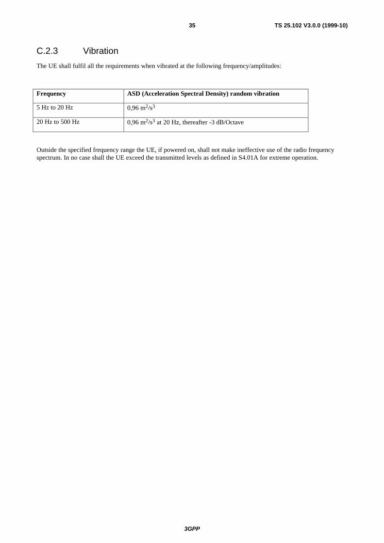
C.2.3 Vibration
The UE shall fulfil all the requirements when vibrated at the following frequency/amplitudes:
Frequency ASD (Acceleration Spectral Density) random vibration
5 Hz to 20 Hz 0,96 m2/s3
20 Hz to 500 Hz 0,96 m2/s3 at 20 Hz, thereafter -3 dB/Octave
Outside the specified frequency range the UE, if powered on, shall not make ineffective use of the radio frequencyspectrum. In no case shall the UE exceed the transmitted levels as defined in S4.01A for extreme operation.

3GPP
TS 25.102 V3.0.0 (1999-10)36
Annex D (informative): Open items
Section number Section description Status
3 Definitions, Symbols,Abbreviations
Update required
5.2 Frequency bands The deployment of TDD in the 1920 MHz to 1980 MHz band isan open item.
6.6.2.2.1 ACLR, Minimum requirement The possibility is being considered of dynamically relaxing theACP requirements for User Equipment(s) under conditions whenthis would not lead to significant interference (with respect toother system scenario or UMTS operators). This would becarried out under network control, primarily to facilitatereduction in UE power consumption.
6.7.2.1 Spectrum emission mask Requirements for other than UE power class 21dBm
6.7.2.2 ACLR Requirements for other than UE power class 21dBm
6.8 Transmit Intermodulation Requirements for other than UE power class 21dBm
6.9.3 Peak Code Domain Error Requirement to be defined.
7.5 ACS Value in square brackets
7.9 Spurious Emissions Values in square brackets
8 Performance Requirement Values are TBD, update of structure needed.
Annex E2 Service ImplementationCapabilities
For further study

3GPP
TS 25.102 V3.0.0 (1999-10)37
ANNEX E (INFORMATIVE): Terminal Capabilities (TDD)This section is based on the LS sent to TSG T2 on baseline terminal capabilities which has been updated to take intoaccount changes in UE radio requirement specifications TS 25.102.
E.1 Baseline Implementation Capabilities
Capability TDD Section UE* Comments
Chiprate 3.84 Mcps 5.1 M
Frequency bands– 1900-1920 MHz– 2010-2025 MHz– Other spectrum
5.2MMO
Declared 1900-1920 MHzDeclared 2010-2025 MHzAs Declared
Carrier raster 5.4 M
UE maximum output power 6.2.1 M At least one power class
(* M = mandatory, O = optional)
E.2 Service Implementation CapabilitiesFor further study.

3GPP
TS 25.102 V3.0.0 (1999-10)38
History
Document history
V0.0.1 1999-02-01 Document created based on S4.01A v0.0.2 “UTRA (UE) FDD, radio transmissionand reception”
V0.0.2 1999-02-25 Editorial update after WG4#2 for distribution on the e-mail reflector.
V1.0.0 1999-03-02 Version presented to TSG RAN for information (identical to version 0.0.2)
V1.0.1 1999-04-13 Update according to decisions at TSG RAN WG4#3 in Tokyo, Japan, sent to WG4e-mail reflector for comments
TS 25.102
V1.0.0
1999-04-23 Noted by TSG-RAN as TS 25.102 V1.0.0
V1.1.0 1999-04-23 Incorporation of agreed changes from WG4#4 Meeting in Kista.
V1.2.0 1999-07-06 Incorporation of agreed changes from WG4#5 Meeting in Miami.
V1.3.0 1999-08-09 Incorporation of agreed changes from WG4#6 Meeting in Edinburgh.
V2.0.0 1999-09-17 Incorporation of agreed changes from WG4#7 Meeting in Tokio.
V2.1.0 1999-10-04 Update after the TSG RAN WG4 AH01 simulation meeting in Noordwijkerhout.Sent to the reflector for comments in advance of TSG RAN#5.
V3.0.0 1999-10-07 Approved by TSG-RAN#5
Editor for TS 25.102 is:
Meik Kottkamp
Siemens AG
Tel: +49 89 722 36223
Fax: +49 89 722 24450
E-Mail: [email protected]
This document is written in Microsoft Word 7