Embed Size (px)
Citation preview
Toshiba Personal Computer
TECRA M1
Maintenance Manual
TOSHIBA CORPORATION
File Number 960-436
ii TECRA M1 Maintenance Manual (960-436)
Copyright
© 2003 by Toshiba Corporation. All rights reserved. Under the copyright laws, this manual cannot be reproduced in any form without the prior written permission of Toshiba. No patent liability is assumed with respect to the use of the information contained herein.
Toshiba Personal Computer TECRA M1 Maintenance Manual
First edition February 2003
Disclaimer
The information presented in this manual has been reviewed and validated for accuracy. The included set of instructions and descriptions are accurate for the TECRA M1 at the time of this manual's production. However, succeeding computers and manuals are subject to change without notice. Therefore, Toshiba assumes no liability for damages incurred directly or indirectly from errors, omissions, or discrepancies between any succeeding product and this manual.
Trademarks
Intel, Intel SpeedStep and Penteium are trade marks or registered trademarks of Intel Corporation or its subsidiaries in the United States and other countries/regions. Windows and Microsoft are registered trademarks of Microsoft Corporation. Photo CD is a trademark owned by its proprietor and used by TOSHIBA under license. Bluetooth is a trademark owned by its proprietor and used by TOSHIBA under license.
TECRA M1 Maintenance Manual (960-436) iii
Preface
This maintenance manual describes how to perform hardware service maintenance for the Toshiba Personal Computer TECRA M1.
The procedures described in this manual are intended to help service technicians isolate faulty Field Replaceable Units (FRUs) and replace them in the field.
SAFETY PRECAUTIONS
Four types of messages are used in this manual to bring important information to your attention. Each of these messages will be italicized and identified as shown below.
DANGER: “Danger” indicates the existence of a hazard that could result in death or serious bodily injury, if the safety instruction is not observed.
WARNING: “Warning” indicates the existence of a hazard that could result in bodily injury, if the safety instruction is not observed.
CAUTION: “Caution” indicates the existence of a hazard that could result in property damage, if the safety instruction is not observed.
NOTE: “Note” contains general information that relates to your safe maintenance service.
Improper repair of the computer may result in safety hazards. Toshiba requires service technicians and authorized dealers or service providers to ensure the following safety precautions are adhered to strictly.
Be sure to fasten screws securely with the right screwdriver. If a screw is not fully fastened, it could come loose, creating a danger of a short circuit, which could cause overheating, smoke or fire.
If you replace the battery pack or RTC battery, be sure to use only the same model battery or an equivalent battery recommended by Toshiba. Installation of the wrong battery can cause the battery to explode.
iv TECRA M1 Maintenance Manual (960-436)
The manual is divided into the following parts:
Chapter 1 Hardware Overview describes the TECRA M1 system unit and each FRU.
Chapter 2 Troubleshooting Procedures explains how to diagnose and resolve FRU problems.
Chapter 3 Test and Diagnostics describes how to perform test and diagnostic operations for maintenance service.
Chapter 4 Replacement Procedures describes the removal and replacement of the FRUs.
Appendices The appendices describe the following:
Handling the LCD module Board layout Pin assignments Keyboard scan/character codes Key layout Wiring diagrams BIOS Rewrite Procedures Reliability
TECRA M1 Maintenance Manual (960-436) v
Conventions
This manual uses the following formats to describe, identify, and highlight terms and operating procedures.
Acronyms
On the first appearance and whenever necessary for clarification acronyms are enclosed in parentheses following their definition. For example:
Read Only Memory (ROM)
Keys
Keys are used in the text to describe many operations. The key top symbol as it appears on the keyboard is printed in boldface type.
Key operation
Some operations require you to simultaneously use two or more keys. We identify such operations by the key top symbols separated by a plus (+) sign. For example, Ctrl + Pause (Break) means you must hold down Ctrl and at the same time press Pause (Break). If three keys are used, hold down the first two and at the same time press the third.
User input
Text that you are instructed to type in is shown in the boldface type below:
DISKCOPY A: B:
The display
Text generated by the computer that appears on its display is presented in the type face below:
Format complete System transferred

vi TECRA M1 Maintenance Manual (960-436)
TECRA M1 Maintenance Manual (960-436) vii
Table of Contents
Chapter 1 Hardware Overview
1.1 Features ...................................................................................................................... 1-1
1.2 System Unit Block Diagram ...................................................................................... 1-9
1.3 3.5-inch Floppy Disk Drive (USB External) ........................................................... 1-16
1.4 2.5-inch Hard Disk Drive......................................................................................... 1-17
1.5 CD-ROM Drive ....................................................................................................... 1-19
1.6 DVD-ROM Drive .................................................................................................... 1-20
1.7 CD-RW/DVD-ROM Drive ...................................................................................... 1-22
1.8 DVD Multi Drive..................................................................................................... 1-24
1.9 Keyboard.................................................................................................................. 1-26
1.10 TFT Color Display................................................................................................... 1-27
1.11 Power Supply ........................................................................................................... 1-29
1.12 Batteries ................................................................................................................... 1-32
Chapter 2 Troubleshooting Procedures
2.1 Troubleshooting ......................................................................................................... 2-1
2.2 Troubleshooting Flowchart........................................................................................ 2-2
2.3 Power Supply Troubleshooting.................................................................................. 2-6
2.4 System Board Troubleshooting................................................................................ 2-16
2.5 FDD Troubleshooting .............................................................................................. 2-30
2.6 HDD Troubleshooting ............................................................................................. 2-33
2.7 Keyboard and Touch pad Troubleshooting.............................................................. 2-38
2.8 Display Troubleshooting.......................................................................................... 2-41
2.9 CD-ROM Drive Troubleshooting ............................................................................ 2-43
2.10 DVD-ROM, CD-RW/DVD-ROM, and DVD Multi Drive Troubleshooting .......... 2-45
2.11 Modem Troubleshooting.......................................................................................... 2-47
2.12 LAN Troubleshooting.............................................................................................. 2-49
2.13 Bluetooth Troubleshooting ...................................................................................... 2-50
viii TECRA M1 Maintenance Manual (960-436)
2.14 Wireless LAN Troubleshooting............................................................................... 2-54
2.15 Sound Troubleshooting............................................................................................ 2-58
2.16 SD Card Slot Troubleshooting................................................................................. 2-61
TECRA M1 Maintenance Manual (960-436) ix
Chapter 3 Tests and Diagnostics
3.1 The Diagnostic Test ................................................................................................... 3-1
3.2 Executing the Diagnostic Test ................................................................................... 3-3
3.3 Subtest Names............................................................................................................ 3-7
3.4 System Test .............................................................................................................. 3-10
3.5 Memory Test ............................................................................................................ 3-13
3.6 Keyboard Test .......................................................................................................... 3-15
3.7 Display Test ............................................................................................................. 3-19
3.8 Floppy Disk Test...................................................................................................... 3-23
3.9 Printer Test............................................................................................................... 3-25
3.10 Async Test ............................................................................................................... 3-27
3.11 Hard Disk Test ......................................................................................................... 3-29
3.12 Real Timer Test........................................................................................................ 3-32
3.13 NDP Test.................................................................................................................. 3-34
3.14 Expansion Test......................................................................................................... 3-35
3.15 CD-ROM/DVD-ROM Test ..................................................................................... 3-36
3.16 Wireless LAN Test (Agere) ..................................................................................... 3-37
3.17 Wireless LAN Test (Atheros) .................................................................................. 3-42
3.18 Wireless LAN Test (Calexico)................................................................................. 3-45
3.19 Sound/Modem Test .................................................................................................. 3-46
3.20 IEEE1394 Test ......................................................................................................... 3-50
3.21 Bluetooth Test.......................................................................................................... 3-52
3.22 Error Code and Error Status Names......................................................................... 3-61
3.23 Hard Disk Test Detail Status ................................................................................... 3-64
3.24 Head Cleaning.......................................................................................................... 3-66
3.25 Log Utilities ............................................................................................................. 3-67
3.26 Running Test ............................................................................................................ 3-69
3.27 Floppy Disk Drive Utilities...................................................................................... 3-71
3.28 System Configuration .............................................................................................. 3-76
3.29 SETUP ..................................................................................................................... 3-78
x TECRA M1 Maintenance Manual (960-436)
Chapter 4 Replacement Procedures
4.1 General ....................................................................................................................... 4-1
4.2 Battery Pack ............................................................................................................... 4-9
4.3 Optional PC Card..................................................................................................... 4-12
4.4 Optional SD Card..................................................................................................... 4-14
4.5 HDD......................................................................................................................... 4-15
4.6 Slim Select Bay Mosule........................................................................................... 4-20
4.7 Modem Daughter Card ............................................................................................ 4-24
4.8 CPU.......................................................................................................................... 4-27
4.9 Keyboard.................................................................................................................. 4-32
4.10 Memory Module ...................................................................................................... 4-36
4.11 Sensor/Switch Board................................................................................................ 4-38
4.12 Touch Pad ................................................................................................................ 4-40
4.13 Wireless LAN Card.................................................................................................. 4-44
4.14 Bluetooth Module .................................................................................................... 4-47
4.15 Display Assembly .................................................................................................... 4-49
4.16 LED Board ............................................................................................................... 4-53
4.17 Sound Board............................................................................................................. 4-55
4.18 System Board/RTC Battery/DC-IN Jack ................................................................. 4-57
4.19 USB Board ............................................................................................................... 4-62
4.20 Fan............................................................................................................................ 4-64
4.21 Display Mask ........................................................................................................... 4-66
4.22 FL Inverter ............................................................................................................... 4-68
4.23 LCD Module ............................................................................................................ 4-70
4.24 Wireless LAN Antenna/Bluetooth Antenna/Display Cover/Speaker ...................... 4-74
4.25 Fluorescent Lamp..................................................................................................... 4-85
TECRA M1 Maintenance Manual (960-436) xi
Appendices
Appendix A Handling the LCD Module ........................................................................... A-1
Appendix B Board Layout ................................................................................................ B-1
Appendix C Pin Assignments............................................................................................ C-1
Appendix D Character Codes ............................................................................................ D-1
Appendix E Key Layout.....................................................................................................E-1
Appendix F Reliability.......................................................................................................F-1
Appendix G BIOS Rewrite Procedures ............................................................................. G-1
Appendix H EC/KBC Rewrite Procedures........................................................................ H-1
Appendix I Reliability........................................................................................................I-1

xii TECRA M1 Maintenance Manual (960-436)
Chapter 1 Hardware Overview

1 Hardware Overview
1-ii TECRA M1 Maintenance Manual (960-436)
1 Hardware Overview
Chapter 1 Contents
1.1 Features.......................................................................................................................1-1
1.2 System Unit Block Diagram.......................................................................................1-9
1.3 3.5-inch Floppy Disk Drive (USB External) ............................................................1-16
1.4 2.5-inch Hard Disk Drive .........................................................................................1-17
1.5 CD-ROM Drive ........................................................................................................1-19
1.6 DVD-ROM Drive .....................................................................................................1-20
1.7 CD-RW/DVD-ROM Drive.......................................................................................1-22
1.8 DVD Multi Drive .....................................................................................................1-24
1.9 Keyboard ..................................................................................................................1-26
1.10 TFT Color Display ...................................................................................................1-27
1.10.1 LCD Module .......................................................................................1-27
1.10.2 FL Inverter Board ...............................................................................1-28
1.11 Power Supply............................................................................................................1-29
1.12 Batteries ....................................................................................................................1-32
1.12.1 Main Battery .......................................................................................1-32
1.12.2 Battery Charging Control....................................................................1-33
1.12.3 RTC battery.........................................................................................1-34
TECRA M1 Maintenance Manual (960-436) 1-iii
1 Hardware Overview
1-iv TECRA M1 Maintenance Manual (960-436)
Figures
Figure 1-1 Front of the computer .....................................................................................1-7
Figure 1-2 System unit configuration...............................................................................1-8
Figure 1-3 System unit block diagram .............................................................................1-9
Figure 1-4 3.5-inch FDD (USB External) ......................................................................1-16
Figure 1-5 2.5-inch HDD ...............................................................................................1-17
Figure 1-6 CD-ROM drive .............................................................................................1-19
Figure 1-7 DVD-ROM drive..........................................................................................1-20
Figure 1-8 CD-RW/DVD-ROM drive ...........................................................................1-22
Figure 1-9 DVD Multi drive ..........................................................................................1-24
Figure 1-10 Keyboard ......................................................................................................1-26
Figure 1-11 LCD module .................................................................................................1-27
Tables
Table 1-1 3.5-inch FDD specifications.........................................................................1-16
Table 1-2 2.5-inch HDD specifications ........................................................................1-17
Table 1-3 CD-ROM drive specifications......................................................................1-19
Table 1-4 DVD-ROM drive specifications...................................................................1-20
Table 1-5 CD-RW/DVD-ROM drive specifications ....................................................1-22
Table 1-6 DVD Multi drive specifications ...................................................................1-24
Table 1-7 LCD module specifications ..........................................................................1-27
Table 1-8 FL inverter board specifications...................................................................1-28
Table 1-9 Power supply output rating...........................................................................1-30
Table 1-10 Battery specifications ...................................................................................1-32
Table 1-11 Time required for quick charges...................................................................1-33
Table 1-12 RTC battery charging/data preservation time...............................................1-34
1.1 Features 1 Hardware Overview
1 Features
1.1 Features
The Toshiba TECRA M1 Personal Computer uses extensive Large Scale Integration (LSI), and Complementary Metal-Oxide Semiconductor (CMOS) technology extensively to provide compact size, minimum weight, low power usage and high reliability. This computer incorporates the following features and benefits: The product configuration is BTO/CTO-compatible so that a system can be designed to suit a specific purpose.
Microprocessor
The TECRA M1 computer is equipped with an Intel Banias Processor, which incorporates a math co-processor, a 32KB L1 cache memory and a 1MB L2 cache memory. The processor runs with one of the following speeds:
Intel Banias Processor 1.30GHz (1.35V) / 1.20GHz (0.85V) •
•
•
•
•
•
•
•
Intel Banias Processor 1.40GHz (1.35V) / 1.20GHz (0.85V)
Intel Banias Processor 1.50GHz (1.35V) / 1.20GHz (0.85V)
Intel Banias Processor 1.60GHz (1.35V) / 1.20GHz (0.85V)
This processor operates at 1.35V-0.8V and 100MHz bus clock. A 32KB level-1 cache memory and a 1MB level-2 cache memory are built in.
Chipset
The TECRA M1 is equipped with Intel Odem, Intel ICH4-M and YEBISU3S.
Video Controller
The computer has a Trident XP4-MCM VGA controller. The internal VRAM is 32MB (64MB is also supported.), DDR250MHz.
Memory
Two expansion memory slots are provided to accommodate 2.5V drive PC2100 DDR-SDRAM memory units with a total capacity of 2GB (2,048MB) maximum.
The following four memory modules are available.
128 MB (16M×16bit×4, 2.5V, SDRAM)
256 MB (16M×16bit×8, 2.5V, SDRAM)
512 MB (32M×8bit×16, 2.5V, SDRAM)
1,024MB (32M×16bit×8, 2.5V, SDRAM)
TECRA M1 Maintenance Manual (960-436) 1-1
1 Hardware Overview 1.1 Features
Built-in HDD
The computer has a 2.5-inch HDD. The following capacities are available.
30/40/50/60GB •
USB FDD
A 3.5-inch FDD accommodates 2HD (1.44MB) or 2DD (720KB) disks.
The FDD is connected to an external USB port.
Slim Select Bay
A CD-ROM, DVD-ROM, CD-RW/DVD-ROM or DVD Multi drive, 2nd HDD or 2nd Battery can be installed in the Slim Select Bay. In addition, a second HDD may be purchased as an option for use in the system.
CD-ROM Drive
A full-size, maximum 24-speed 640MB CD-ROM drive, contains an AT Attachment Packet Interface (ATAPI) controller, and supports the following formats: CD-DA, CD-ROM (Mode 1, Mode 2), CD-ROM XA Mode 2, Photo-CD (Single/multi-session), and Enhanced CD.
DVD-ROM Drive
A full-size and runs either 12cm (4.72-inch) or 8cm (3.15-inch) DVD/CDs without an adaptor. It plays DVDs at maximum 8-speed and reads CDs at maximum 24-speed.
CD-RW/DVD Drive
A full-size, CD-RW/DVD drive that contains an AT Attachment Packet Interface (ATAPI) controller. This drive reads CD-R at maximum 24-speed and reads DVD-ROM at maximum 8-speed.
DVD Multi Drive
This drive is a combination of DVD-ROM and CD-R/RW Drive. It is full-size and runs either 12cm (4.72-inch) or 8cm (3.15-inch) DVD/CDs without an adaptor. It plays DVDs at maximum 8-speed, writes CD-R at maximum 8-speed, writes CD-RW at maximum 4-speed, and reads CDs at maximum 24-speed.
1-2 TECRA M1 Maintenance Manual (960-436)
1.1 Features 1 Hardware Overview
Display
The display comes in the following three types:
14.1” XGA-TFT color display, resolution 1,024×768, 16M colors •
• 14.1” SXGA+-TFT color display, resolution 1,400×1,050, 16M colors
In addition, a video controller and an 32/64MB VRAM enables an external monitor to display 16M colors at a resolution of 1,024×768 pixels or 256 colors at a resolution of 1,400×1,050 pixels.
Keyboard
An-easy-to-use 85(US)/86(UK)-key keyboard provides a numeric keypad overlay for fast numeric data entry or for cursor and page control. The keyboard also includes two keys that have special functions in Microsoft Windows 2000/XP. It supports software that uses a 101- or 102-key enhanced keyboard.
Batteries
The computer has two batteries: a rechargeable Lithium-Ion main battery pack and RTC battery (that backs up the Real Time Clock and CMOS memory).
Universal Serial Bus (USB2.0)
Three USB ports are provided. The ports comply with the USB2.0 standard, which enables data transfer speeds 40 times faster than USB1.1 standard. USB1.1 is also supported.
IEEE 1394 port
The computer comes with one IEEE 1394 port. It enables high-speed data transfer directly from external devices such as digital video cameras.
Parallel port
The parallel port enables connection of parallel printer or other parallel devices. (ECP compatible)
Serial port
A standard, 9-pin, serial port enables connection of such serial devices as a serial printer, mouse or modem. A Universal Asynchronous Receiver/Transmitter (UART) is 16550A equivalent.
TECRA M1 Maintenance Manual (960-436) 1-3
1 Hardware Overview 1.1 Features
External monitor port
The port enables connection of an external monitor, which is recognized automatically by Video Electronics Standards Association (VESA) Display Data Channel (DDC) 2B compatible functions.
PS/2 mouse/keyboard port
Either a PS/2 compatible keyboard or a PS/2 compatible mouse can be connected to the port.
PC card slot
The PC card slot (PCMCIA) accommodates two 5mm Type II card or one Type III card. The slot support 16-bit PC cards and Card Bus PC cards. CardBus supports 32-bit PC cards.
SD Card
An SD Card Slot can accommodate Secure Digital flash memory cards with various capacities. SD cards let you easily transfer data from devices, such as digital cameras and Personal Digital Assistants, that use SD Card flash-memory.
Docking interface port
The docking interface port enables connection of an optional Advanced Port Replicator II. It provides additional features as follows:
RJ-45 LAN jack, RT11 Modem jack •
•
•
•
•
•
•
•
•
External monitor port
Parallel port and Serial port
PS/2 Mouse port and Keyboard port
DC IN socket
Security lock slot
Audio line-in, line out jack
Two USB ports and an IEEE 1394 port
DVI port
TOSHIBA Dual Pointing Device
The TOSHIBA Dual Pointing Device consists of Touch Pad and AccuPoint. The touch pad and control buttons enable control of the on-screen pointer and scrolling of windows. The pointer control stick, AccuPoint enables convenient control of the cuesor.
1-4 TECRA M1 Maintenance Manual (960-436)
1.1 Features 1 Hardware Overview
Infrared port
The infrared port is compatible with Fast InfraRed (FIR) standards enabling cableless 4 Mbps, 1.152 Mbps, 115.2 kbps, 57.6 kbps, 38.4 kbps, 19.2 kbps or 9.6 kbps data transfer with Infrared Data Association (IrDA) 1.1 compatible external devices.
Sound system
The sound system is equipped with the following features:
AC Link and AnalogDeveices AD1981A •
•
•
•
•
•
•
AMP: AN12490 and NSCLM4911
Stereo speakers
Built-in Microphone (Mono)
Volume control knob
Stereo Headphone jack
External microphone jack
Video-out jack
The video jack enables to transfer NTSC or PAL data to external devices connected with S-Video cable.
Internal modem
The internal modem is equipped as a modem daughter card (MDC).
The internal modem provides capability for data and fax communication and supports V.90/92. For data reception it operates at 56,000bps and for data transmission it operates at 33,600bps. For fax transmission it operates at 14,400bps. It is also equipped with Speakerphone and TAM (Telephony Answering Machine) function. The speed of data transfer and fax depends on analog telephone line conditions. It has an RJ11 modem jack for connecting to a telephone line. Both of V.90 and V.92 is supported in USA and Canada. In other regions, only V.90 is available.
Internal LAN
The computer is equipped with LAN circuits that support Ethernet LAN (10 megabits per second, 10BASE-T), Fast Ethernet LAN (100 megabits per second, 100 BASE-Tx) and Gigabit Ethernet LAN (1000megabits per second, 1000BASE-T). It also supports Wakeup on LAN (WOL) and Magic Packet.
TECRA M1 Maintenance Manual (960-436) 1-5
1 Hardware Overview 1.1 Features
Bluetooth (BTO)
The computer is equipped with Bluetooth (V1.1) communications standards enable wireless connection between electronic devices such as computers and printers.
Mini PCI Card slot (1 slot, BTO)
In some models built to order (BTO), a Mini PCI Card with wireless LAN functions is available.
Wireless LAN: The Mini PCI Card for wireless LAN is compatible with other LAN systems based on Direct Sequence Spread Spectrum radio technology that complies with the IEEE 802.11 Standard (Revision B) only, and IEEE 802.11 Standard (Revision A, B). Revision A supports data transfer up to 54Mbit/s. Revision B supports data transfer up to 11Mbit/s. It has Frequency Channel Selection (5GHz: Revision A/2.4GHz: Revision B) and allows roaming over multiple channels.
Presentation button
This button switches the display between internal display, external display, simultaneous display and multi-monitor display.
Brightness sensor
The Brightness sensor adjusts the brightness of LCD to the adequate brightness according to the illuminant of the place where you are using the PC.
1-6 TECRA M1 Maintenance Manual (960-436)
1.1 Features 1 Hardware Overview
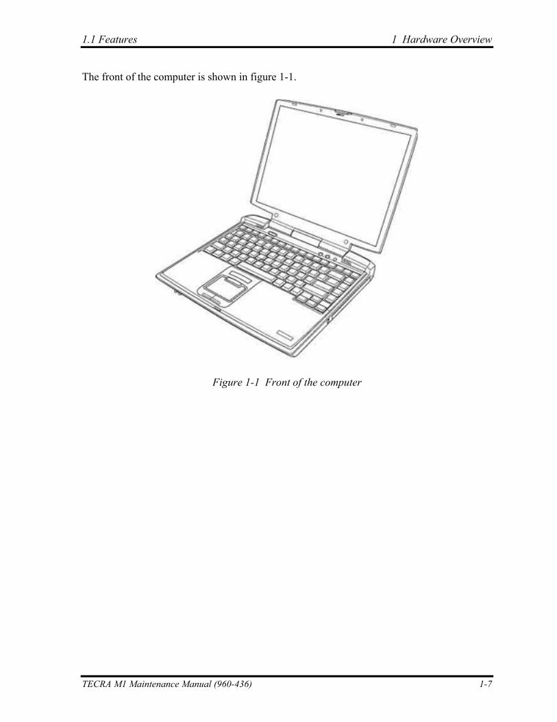
The front of the computer is shown in figure 1-1.
Figure 1-1 Front of the computer
TECRA M1 Maintenance Manual (960-436) 1-7
1 Hardware Overview 1.1 Features
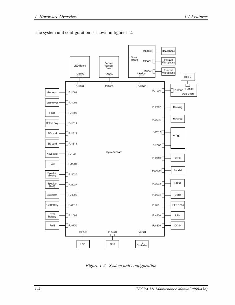
The system unit configuration is shown in figure 1-2.
MDC
Figure 1-2 System unit configuration
1-8 TECRA M1 Maintenance Manual (960-436)
1.2 System Unit Block Diagram 1 Hardware Overview
1.2 System Unit Block Diagram
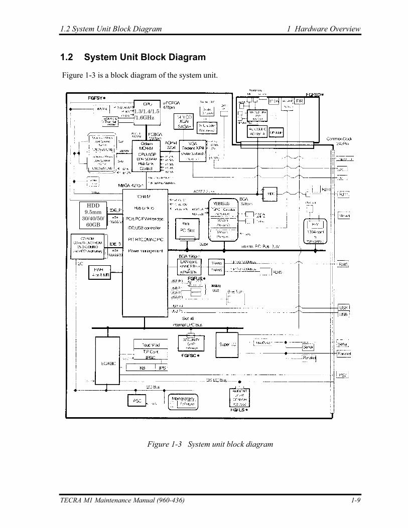
Figure 1-3 is a block diagram of the system unit.
1.3/1.4/1.5/1.6GHz
HDD9.5mm30/40/50/60GB
Figure 1-3 System unit block diagram
TECRA M1 Maintenance Manual (960-436) 1-9
1 Hardware Overview 1.2 System Unit Block Diagram
The system unit is composed of the following major components:
Processor
• Intel Banias Processor 1.30GHz – Processor core speed: 1.30GHz (Performance Mode at 1.35V) and 1.20GHz
(Battery Optimized Mode at 0.85V) – Processor bus speed: 400MHz – Integrated L1 cache memory: 32KB instruction cache and 32KB write-back
data cache, 4-way set associative – Integrated L2 cache memory: 1MB ECC protected cache data array, 8-way set
associative – Integrated NDP
• Intel Banias Processor 1.40GHz – Processor core speed: 1.40GHz (Performance Mode at 1.35V) and 1.20GHz
(Battery Optimized Mode at 0.85V) – Processor bus speed: 400MHz – Integrated L1 cache memory: 32KB instruction cache and 32KB write-back
data cache, 4-way set associative – Integrated L2 cache memory: 1MB ECC protected cache data array, 8-way set
associative – Integrated NDP
• Intel Banias Processor 1.50GHz – Processor core speed: 1.50GHz (Performance Mode at 1.35V) and 1.20GHz
(Battery Optimized Mode at 0.85V) – Processor bus speed: 400MHz – Integrated L1 cache memory: 32KB instruction cache and 32KB write-back
data cache, 4-way set associative – Integrated L2 cache memory: 1MB ECC protected cache data array, 8-way set
associative – Integrated NDP
• Intel Banias Processor 1.60GHz – Processor core speed: 1.60GHz (Performance Mode at 1.35V) and 1.20GHz
(Battery Optimized Mode at 0.85V) – Processor bus speed: 400MHz – Integrated L1 cache memory: 32KB instruction cache and 32KB write-back
data cache, 4-way set associative – Integrated L2 cache memory: 1MB ECC protected cache data array, 8-way set
associative – Integrated NDP
1-10 TECRA M1 Maintenance Manual (960-436)
1.2 System Unit Block Diagram 1 Hardware Overview
Memory
Two BTO-compatible expansion memory slots are provided. Expansion up to 2GB (2,048MB) is available.
• DDR-SDRAM (Double Data Rate - Synchronous DRAM) • 128 MB/256 MB/512 MB/1,024MB(1GB) selectable
– 128 MB (16M×16bit×4) – 256 MB (16M×16bit×8) – 512 MB (32M×8bit×16) – 1,024MB (32M×16bit 8)
• 200 pin, SO Dual In-line Memory Modules (SO-DIMM) • 2.5 volt operation • Supports DDR CL2/2.5 • Supports PC2100 only
Intel Odem (North Bridge)
• One Intel 82845MP is used. • Features:
– Banias Processor System Bus Support – DRAM Controller: DDR200/DDR266 Support, 1GB max – Accelerated Graphics Port Interface: adheres to AGP2.0, AGP×4 mode – Hub Link Interface – 593-ball 37.5×37.5 mm FC-BGA package
Intel ICH4-M (South Bridge)
• One Intel 82801LAM is used. • This gate array has the following features:
– Hub Link Interface – PCI Rev2.2 Interface (6 PCI REQ/GNT Pairs) – BusMaster IDE Controller (Ultra ATA 100/66/33) – USB 1.1/2.0 Controller 6 Prots (EHCI: Enhanced Host Controller) – I/O APIC (ACPI 1.06) – SMBus2.0 Controller – FWH Interface (BIOS) – LPC Interface (EC/KBC, Super I/O) – IRQ Controller – Serial Interrupt Controller – Power Management Controller – Deeper Sleep (C4) Support – Suspend/Resume Control – AC'97 2.2 Interface – Internal RTC
TECRA M1 Maintenance Manual (960-436) 1-11
1 Hardware Overview 1.2 System Unit Block Diagram
– Internal LAN Controller (WfM2.0) – 421-ball 31×31mm BGA Package
PC Card Controller Gate Array
• One YEBISU3S gate array is used. • This gate array has the following functions and components.
– PCI interface (PCI Revision2.2) – CardBus/PC Card controller (Yenta2 Version2.2) – SD memory card controller (SDHC Ver.1.2) – SD IO card controller (Ver.1.0) – SmartMedia controller (SMHC Ver.01/SMIL1.0) – SIO (UART) controller (MS Debug Port Specification Ver.1.0) – Docking station interface – Q switch control, reset control – External device interface
Firmware Hub (FWH)
• One Intel 82802AB8 is used. • This gate array has the following features:
– Intel platform compatibility – Firmware hub hardware interface mode – Industry-standard packages – Two configurable interfaces – 4Mbits of flash memory for platform code/data nonvolatile storage – Address/Address-Multiplexed (A/A Mux) interface/mode – Case temperature operating range – Vcc: 3.3V ± 0.3V – Vpp: 3.3V and 12V for fast programming (80 hours maximum)
• 4Mbits of flash memory are used as shown below: – 64KB are used for VGA-BIOS. – 192KB are used for system BIOS. – 8KB are used for plug and play data area. – 8KB are used for password security. – 16KB are used for boot strap. – 64KB are used for ACPI P code. – 64KB are used for LOGO. – 64KB are reserved for LAN BIOS. – 32KB are reserved.
1-12 TECRA M1 Maintenance Manual (960-436)
1.2 System Unit Block Diagram 1 Hardware Overview
VGA Controller
One Trident XP4-MCM chip is used. The video controller incorporates graphics accelerator, video accelerator. • Internal VRAM, 32MB DDR 250MHz (64MB is also supported.) • Connected to AGP bus R2.0 • LCD Interface LVDS 2ch • TV Encoder: Tvxpress2 • DVI Supported by Dock
Sound Controller
• One AC'97Codec AD1981A chip and AC-Link controller embedded in ICH4-M • SW sound
EC/KBC (Embedded Controller/Keyboard Controller)
• One Mitsubishi M306K9FCLRP micon chip functions as both EC and KBC. • EC This controller controls the following functions:
– Power supply sequence – Thermal conditions – LEDs – Beep – Device ON/OFF – Fan speed – Universal I/O port – Docker Docking Sequence – Battery capacity check – Forced reset – Flash rewriting – EC interface – I2C communication – EC access – Slim Select Bay Control
• KBC
This controller has the following functions: – Scan controller to check status of keyboard matrix – Interface controller between the keyboard scan controller and the system – Control of switching and simultaneous operation of the accupoint/external
PS/2 mouse and of the internal keyboard/external PS/2 keyboard
TECRA M1 Maintenance Manual (960-436) 1-13
1 Hardware Overview 1.2 System Unit Block Diagram
PSC (Power Supply Controller)
• One TMP87PM48U chip is used. • This controller controls the power sources.
RS232 Driver
• One MAXIM3243 chip is used. • This driver converts signals for interface with external equipment.
Clock Generator
• One ICS950810AG-T is used. • This device generates the system clock.
Modem Controller
• One built-in modem card with Xircom Lucent SCORPIO+CSP1037B is used. • This controller has the following functions:
– Digital line protection support – Ring wake up support – AC97 interface – The following communication codes are supported
Data: V.90 (56K bps) data communication control V.92 (56K bps) data communication control V.34 (33.6 K~2400) V.32 bis (14.4K, 12K, 9600) V.22 bis (2400, 1200) V.22 (1200) V.23 (1200, 600, 75) V.21 (300) Fax: V.17 (14.4K, 12K, 9600, 7200) V.29 (9600, 7200, 4800) V.27 ter (4800, 2400) V.21 ch2 (300)
1-14 TECRA M1 Maintenance Manual (960-436)
1.2 System Unit Block Diagram 1 Hardware Overview
Internal LAN Controller
• One MAC incorporated with ICH4-M and PHY (Kinnereth-R 182562EP or Kenai32N) are used for the internal chip, and are connected with RJ11/RJ45 combo connector.
• This controller has the following functions: • Full Duplex support at 10 Mbps/100 Mbps
– WOL support – Magic Packet Support
Wireless LAN
• One Mini PCI card for LAN with TI card bus controller, TI 1410 is used. Super I/O
• One LPC 47N227 chip is used. • This gate array has the following features:
– Floppy Disk Controller – Serial Port Controller – Infrared Communications Controller – Parallel Port Controller
IEEE1394
• One TSB43AB22 is used.
Sensor
• Thermal Sensor: One ADM1032AR chip is used. • LCD Sensor: One NRS-701-1015T chip is used. • Light Sensor: One TSL2550 chip is used.
TECRA M1 Maintenance Manual (960-436) 1-15
1 Hardware Overview 1.3 3.5-inch Floppy Disk Drive (USB External)
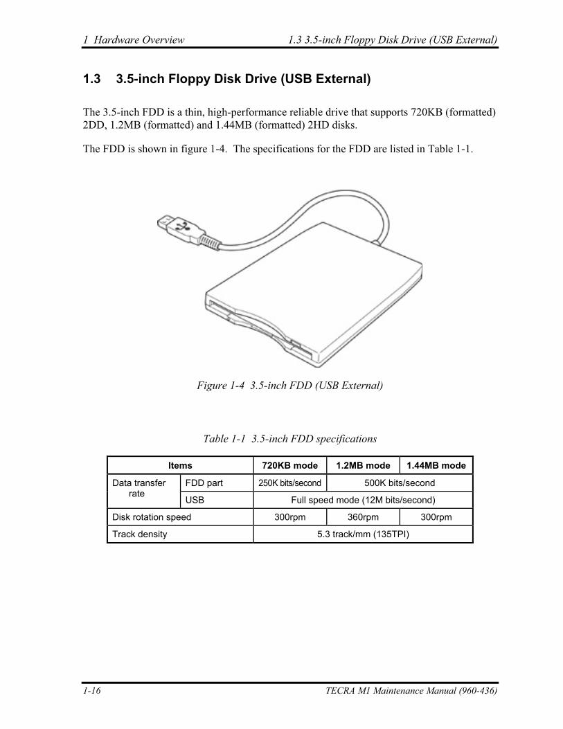
1.3 3.5-inch Floppy Disk Drive (USB External)
The 3.5-inch FDD is a thin, high-performance reliable drive that supports 720KB (formatted) 2DD, 1.2MB (formatted) and 1.44MB (formatted) 2HD disks.
The FDD is shown in figure 1-4. The specifications for the FDD are listed in Table 1-1.
Figure 1-4 3.5-inch FDD (USB External)
Table 1-1 3.5-inch FDD specifications
Items 720KB mode 1.2MB mode 1.44MB mode
FDD part 250K bits/second 500K bits/second Data transfer rate
USB Full speed mode (12M bits/second)
Disk rotation speed 300rpm 360rpm 300rpm
Track density 5.3 track/mm (135TPI)
1-16 TECRA M1 Maintenance Manual (960-436)
1.4 2.5-inch Hard Disk Drive 1 Hardware Overview
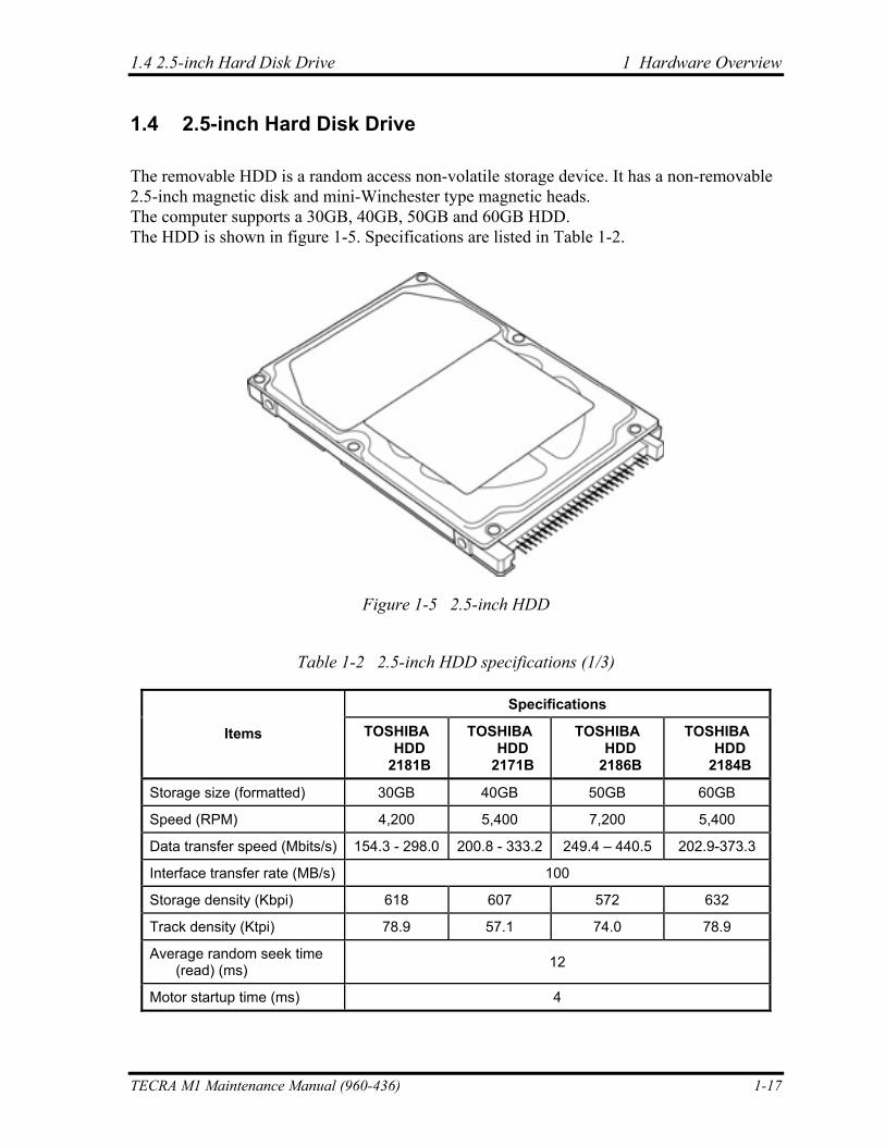
1.4 2.5-inch Hard Disk Drive
The removable HDD is a random access non-volatile storage device. It has a non-removable 2.5-inch magnetic disk and mini-Winchester type magnetic heads. The computer supports a 30GB, 40GB, 50GB and 60GB HDD. The HDD is shown in figure 1-5. Specifications are listed in Table 1-2.
Figure 1-5 2.5-inch HDD
Table 1-2 2.5-inch HDD specifications (1/3)
Specifications
Items TOSHIBA HDD
2181B
TOSHIBA HDD
2171B
TOSHIBA HDD
2186B
TOSHIBA HDD
2184B
Storage size (formatted) 30GB 40GB 50GB 60GB
Speed (RPM) 4,200 5,400 7,200 5,400
Data transfer speed (Mbits/s) 154.3 - 298.0 200.8 - 333.2 249.4 – 440.5 202.9-373.3
Interface transfer rate (MB/s) 100
Storage density (Kbpi) 618 607 572 632
Track density (Ktpi) 78.9 57.1 74.0 78.9
Average random seek time (read) (ms) 12
Motor startup time (ms) 4
TECRA M1 Maintenance Manual (960-436) 1-17
1 Hardware Overview 1.4 2.5-inch Hard Disk Drive
Table 1-2 2.5-inch HDD specifications (2/3)
Specifications Items HITACHI
G8BC0000F310 HITACHI
G8BC00009110
Storage size (formatted) 30GB 40GB
Speed (RPM) 4,200 5,400
Data transfer speed (Mbits/s) 22.1 – 42.8 27.8 – 44.1
Interface transfer rate (MB/s) 100 (MAX Ultra DMA mode)
Storage desnity (Kbpi) 716 612
Track density (Ktpi) 70.0 63.0
Average random seek time (read) (ms) 13
Motor startup time (ms) 5
Table 1-2 2.5-inch HDD specifications (3/3)
Specifications Items IBM
G8BC00004210 IBM
G8BC0000A110
Storage size (formatted) 30GB 40GB
Speed (RPM) 4,200 5,400
Data transfer speed (Mbits/s) 125 – 241 160 – 297
Interface transfer rate (MB/s) 100
Storage desnity (Kbpi) 509 506 (MAX)
Track density (Ktpi) 66.4
Average random seek time (read) (ms) 12
Motor startup time (ms) 5
1-18 TECRA M1 Maintenance Manual (960-436)
1.5 CD-ROM Drive 1 Hardware Overview
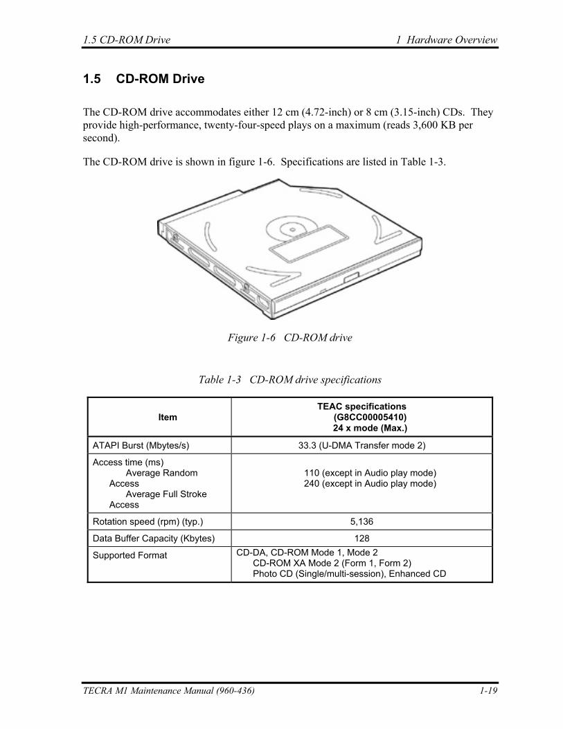
1.5 CD-ROM Drive
The CD-ROM drive accommodates either 12 cm (4.72-inch) or 8 cm (3.15-inch) CDs. They provide high-performance, twenty-four-speed plays on a maximum (reads 3,600 KB per second).
The CD-ROM drive is shown in figure 1-6. Specifications are listed in Table 1-3.
Figure 1-6 CD-ROM drive
Table 1-3 CD-ROM drive specifications
Item
TEAC specifications (G8CC00005410) 24 x mode (Max.)
ATAPI Burst (Mbytes/s) 33.3 (U-DMA Transfer mode 2)
Access time (ms) Average Random Access Average Full Stroke Access
110 (except in Audio play mode) 240 (except in Audio play mode)
Rotation speed (rpm) (typ.) 5,136
Data Buffer Capacity (Kbytes) 128
Supported Format CD-DA, CD-ROM Mode 1, Mode 2 CD-ROM XA Mode 2 (Form 1, Form 2) Photo CD (Single/multi-session), Enhanced CD
TECRA M1 Maintenance Manual (960-436) 1-19
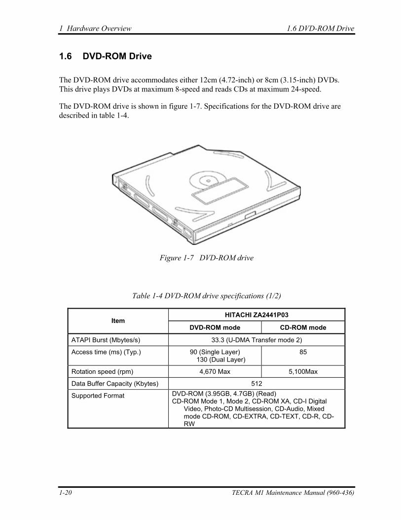
1 Hardware Overview 1.6 DVD-ROM Drive
1.6 DVD-ROM Drive
The DVD-ROM drive accommodates either 12cm (4.72-inch) or 8cm (3.15-inch) DVDs. This drive plays DVDs at maximum 8-speed and reads CDs at maximum 24-speed.
The DVD-ROM drive is shown in figure 1-7. Specifications for the DVD-ROM drive are described in table 1-4.
Figure 1-7 DVD-ROM drive
Table 1-4 DVD-ROM drive specifications (1/2)
HITACHI ZA2441P03 Item
DVD-ROM mode CD-ROM mode
ATAPI Burst (Mbytes/s) 33.3 (U-DMA Transfer mode 2)
Access time (ms) (Typ.) 90 (Single Layer) 130 (Dual Layer)
85
Rotation speed (rpm) 4,670 Max 5,100Max
Data Buffer Capacity (Kbytes) 512
Supported Format DVD-ROM (3.95GB, 4.7GB) (Read) CD-ROM Mode 1, Mode 2, CD-ROM XA, CD-I Digital
Video, Photo-CD Multisession, CD-Audio, Mixed mode CD-ROM, CD-EXTRA, CD-TEXT, CD-R, CD-RW
1-20 TECRA M1 Maintenance Manual (960-436)
1.6 DVD-ROM Drive 1 Hardware Overview
Table 1-4 DVD-ROM drive specifications (2/2)
HITACHI G8CC00015410 Item
DVD-ROM mode CD-ROM mode
ATAPI Burst (Mbytes/s) 33.3 (U-DMA Transfer mode 2)
Access time (ms) Average Random Access
110 (Typ.)
85 (Typ.)
Rotation speed (rpm) 4,594 Max 5,136Max
Data Buffer Capacity (Kbytes) 256
Supported Format DVD-ROM, DVD-R (Read) CD-DA, CD+(E)G, CD-MIDI, CD-TEXT CD-ROM, CD-ROM XA, CD-I CD-I Bridge (Photo-CD, Video-CD) Multisession CD (Photo-CD, CD-EXTRA, CD-R, CD-RW) CD-R (Read), CD-RW (Read)
TECRA M1 Maintenance Manual (960-436) 1-21
1 Hardware Overview 1.7 CD-RW/DVD-ROM Drive
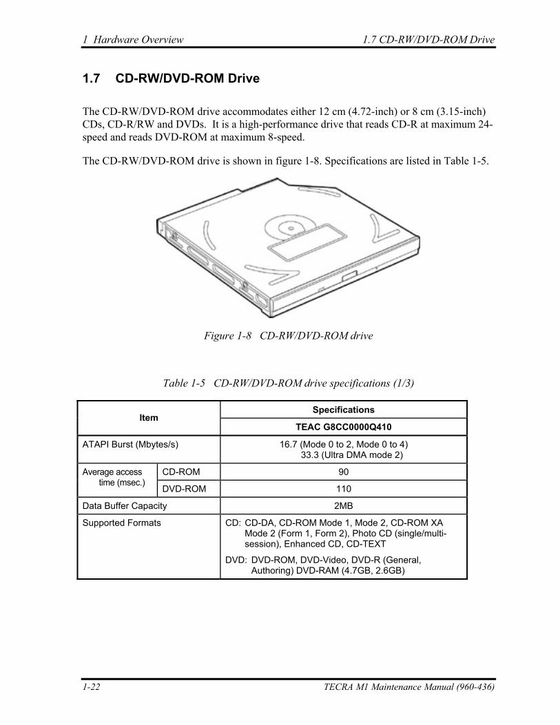
1.7 CD-RW/DVD-ROM Drive
The CD-RW/DVD-ROM drive accommodates either 12 cm (4.72-inch) or 8 cm (3.15-inch) CDs, CD-R/RW and DVDs. It is a high-performance drive that reads CD-R at maximum 24-speed and reads DVD-ROM at maximum 8-speed.
The CD-RW/DVD-ROM drive is shown in figure 1-8. Specifications are listed in Table 1-5.
Figure 1-8 CD-RW/DVD-ROM drive
Table 1-5 CD-RW/DVD-ROM drive specifications (1/3)
Specifications Item
TEAC G8CC0000Q410
ATAPI Burst (Mbytes/s) 16.7 (Mode 0 to 2, Mode 0 to 4) 33.3 (Ultra DMA mode 2)
CD-ROM 90 Average access time (msec.)
DVD-ROM 110
Data Buffer Capacity 2MB
Supported Formats CD: CD-DA, CD-ROM Mode 1, Mode 2, CD-ROM XA Mode 2 (Form 1, Form 2), Photo CD (single/multi-session), Enhanced CD, CD-TEXT
DVD: DVD-ROM, DVD-Video, DVD-R (General, Authoring) DVD-RAM (4.7GB, 2.6GB)
1-22 TECRA M1 Maintenance Manual (960-436)
1.7 CD-RW/DVD-ROM Drive 1 Hardware Overview
Table 1-5 CD-RW/DVD-ROM drive specifications (2/3)
Specifications Item
Panasonic G8CC00010410
ATAPI Burst (Mbytes/s) 16.6 (PIO Mode 4, DMA Mode 2) 33.3 (Ultra DMA Mode2)
CD-ROM 130 Average access time (msec.)
DVD-ROM 180
Data Buffer Capacity 2MB
Supported Formats CD: CD-DA, CD-ROM, CD-ROM XA, CD-R, CD-RW Photo CD, Video CD, CD-EXTRA (CD+), CD-TEXT
DVD: DVD-Video, DVD-ROM, DVD-R (3.9GB, 4.7GB), DVD-RW, DVD-RAM (4.7GB)
Table 1-5 CD-RW/DVD-ROM drive specifications (3/3)
Specifications Item
HITACHI G8CC00016410
ATAPI Burst (Mbytes/s) 16.6 (PIO Mode 4, DMA MW Mode 2) 33.3 (Ultra DMA Mode2)
CD-ROM 120 Average access time (msec.)
DVD-ROM 110
Data Buffer Capacity 2MB
Supported Formats CD: CD-ROM Mode-1, CD-ROM XA, CD-Audio, Mixed Mode CD-ROM, Photo-CD, CD-I DV, Video CD, CD-Plus/CD-EXTRA, CD-TEXT, CD-R, CD-RW
DVD: DVD-ROM (single layer 4.7GB, dual layer 8.5GB) DVD-R (3.95/4.7GB), DVD-RW (4.7GB)
TECRA M1 Maintenance Manual (960-436) 1-23
1 Hardware Overview 1.8 DVD Multi Drive
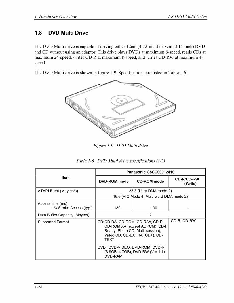
1.8 DVD Multi Drive
The DVD Multi drive is capable of driving either 12cm (4.72-inch) or 8cm (3.15-inch) DVD and CD without using an adaptor. This drive plays DVDs at maximum 8-speed, reads CDs at maximum 24-speed, writes CD-R at maximum 8-speed, and writes CD-RW at maximum 4-speed.
The DVD Multi drive is shown in figure 1-9. Specifications are listed in Table 1-6.
Figure 1-9 DVD Multi drive
Table 1-6 DVD Multi drive specifications (1/2)
Panasonic G8CC00012410 Item
DVD-ROM mode CD-ROM mode CD-R/CD-RW (Write)
ATAPI Burst (Mbytes/s) 33.3 (Ultra DMA mode 2) 16.6 (PIO Mode 4, Multi-word DMA mode 2)
Access time (ms) 1/3 Stroke Access (typ.)
180
130 -
Data Buffer Capacity (Mbytes) 2
Supported Format CD: CD-DA, CD-ROM, CD-R/W, CD-R, CD-ROM XA (except ADPCM), CD-I Ready, Photo CD (Multi session), Video CD, CD-EXTRA (CD+), CD-TEXT
DVD: DVD-VIDEO, DVD-ROM, DVD-R (3.9GB, 4.7GB), DVD-RW (Ver.1.1), DVD-RAM
CD-R, CD-RW
1-24 TECRA M1 Maintenance Manual (960-436)
1.8 DVD Multi Drive 1 Hardware Overview
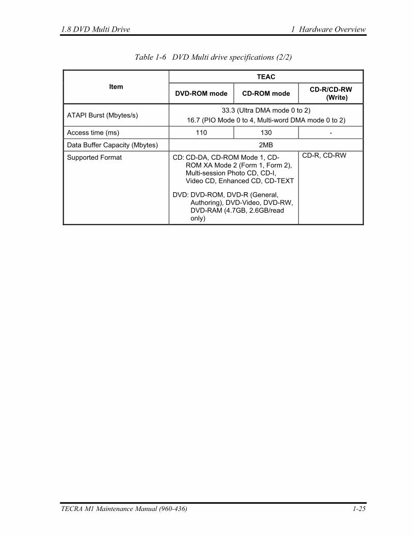
Table 1-6 DVD Multi drive specifications (2/2)
TEAC Item
DVD-ROM mode CD-ROM mode CD-R/CD-RW (Write)
ATAPI Burst (Mbytes/s) 33.3 (Ultra DMA mode 0 to 2)
16.7 (PIO Mode 0 to 4, Multi-word DMA mode 0 to 2)
Access time (ms) 110 130 -
Data Buffer Capacity (Mbytes) 2MB
Supported Format CD: CD-DA, CD-ROM Mode 1, CD-ROM XA Mode 2 (Form 1, Form 2), Multi-session Photo CD, CD-I, Video CD, Enhanced CD, CD-TEXT
DVD: DVD-ROM, DVD-R (General, Authoring), DVD-Video, DVD-RW, DVD-RAM (4.7GB, 2.6GB/read only)
CD-R, CD-RW
TECRA M1 Maintenance Manual (960-436) 1-25
1 Hardware Overview 1.9 Keyboard
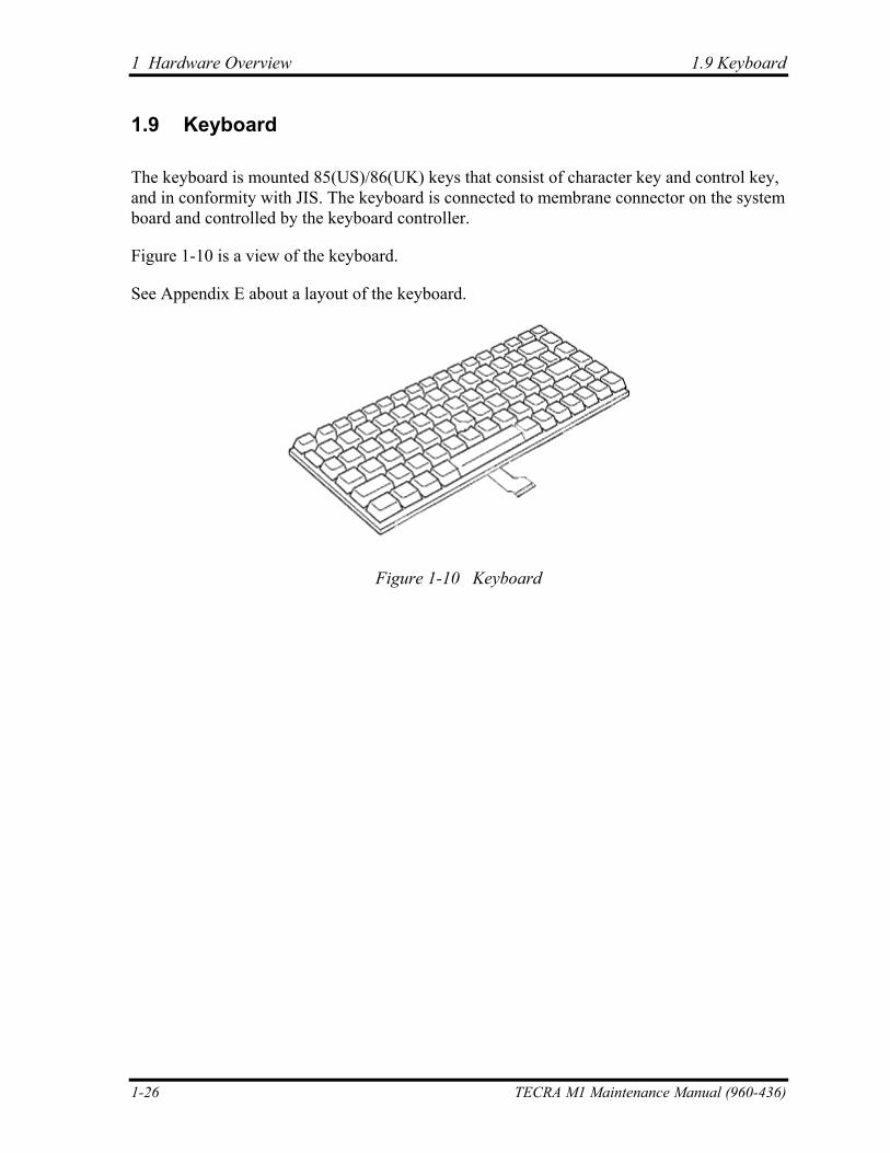
1.9 Keyboard
The keyboard is mounted 85(US)/86(UK) keys that consist of character key and control key, and in conformity with JIS. The keyboard is connected to membrane connector on the system board and controlled by the keyboard controller.
Figure 1-10 is a view of the keyboard.
See Appendix E about a layout of the keyboard.
Figure 1-10 Keyboard
1-26 TECRA M1 Maintenance Manual (960-436)
1.10 TFT Color Display 1 Hardware Overview
1.10 TFT Color Display
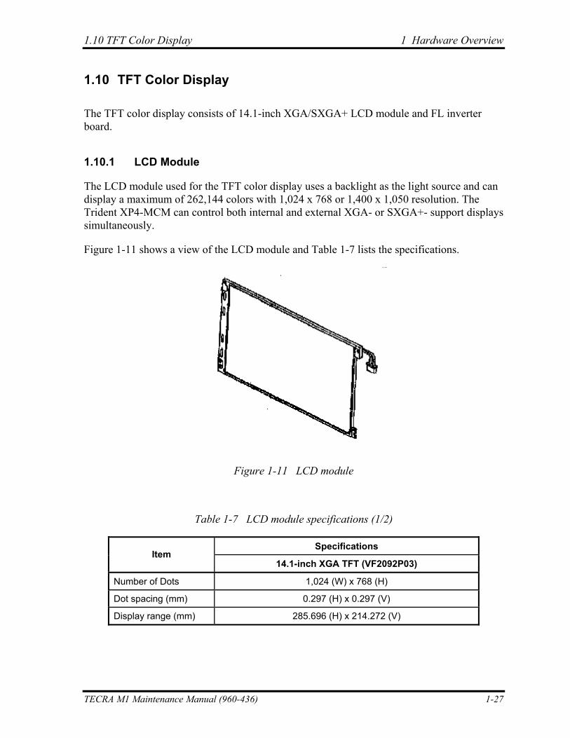
The TFT color display consists of 14.1-inch XGA/SXGA+ LCD module and FL inverter board.
1.10.1 LCD Module
The LCD module used for the TFT color display uses a backlight as the light source and can display a maximum of 262,144 colors with 1,024 x 768 or 1,400 x 1,050 resolution. The Trident XP4-MCM can control both internal and external XGA- or SXGA+- support displays simultaneously.
Figure 1-11 shows a view of the LCD module and Table 1-7 lists the specifications.
Figure 1-11 LCD module
Table 1-7 LCD module specifications (1/2)
Specifications Item
14.1-inch XGA TFT (VF2092P03)
Number of Dots 1,024 (W) x 768 (H)
Dot spacing (mm) 0.297 (H) x 0.297 (V)
Display range (mm) 285.696 (H) x 214.272 (V)
TECRA M1 Maintenance Manual (960-436) 1-27
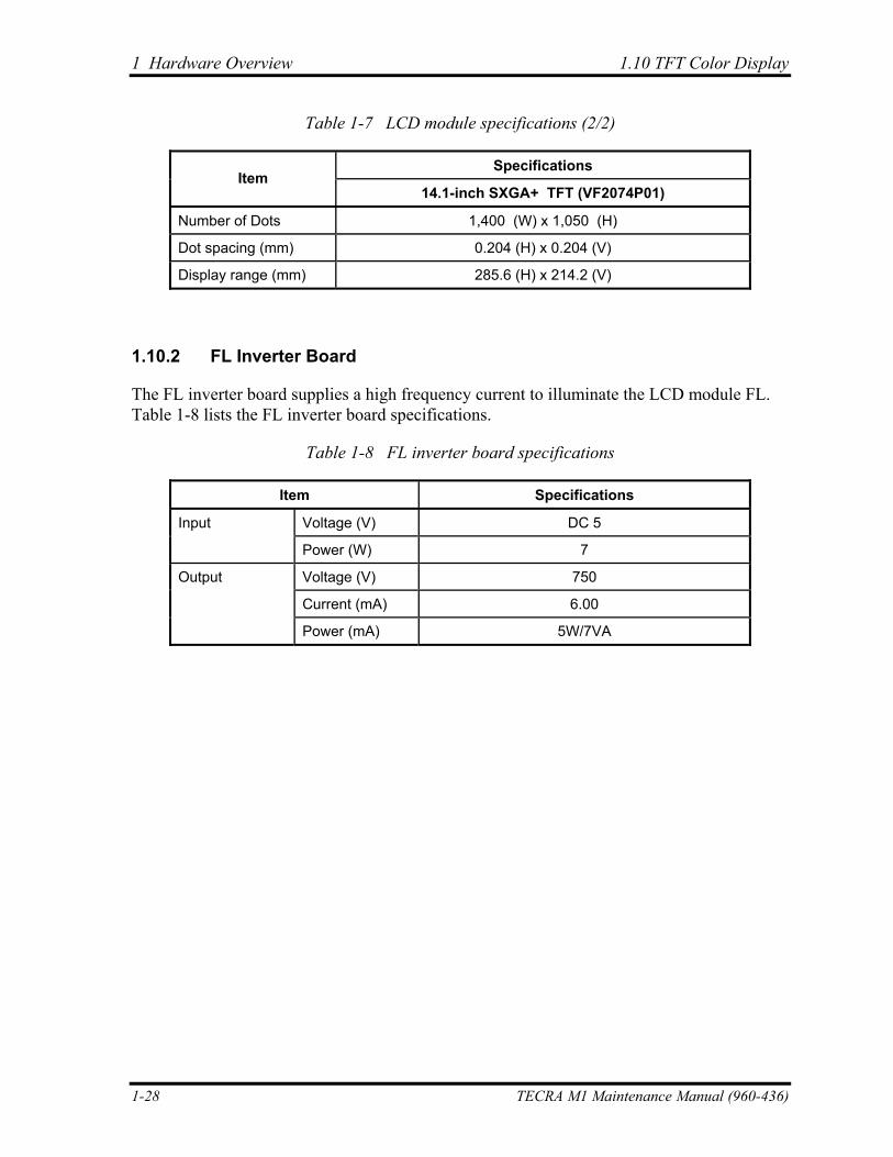
1 Hardware Overview 1.10 TFT Color Display
Table 1-7 LCD module specifications (2/2)
Specifications Item
14.1-inch SXGA+ TFT (VF2074P01)
Number of Dots 1,400 (W) x 1,050 (H)
Dot spacing (mm) 0.204 (H) x 0.204 (V)
Display range (mm) 285.6 (H) x 214.2 (V)
1.10.2 FL Inverter Board
The FL inverter board supplies a high frequency current to illuminate the LCD module FL. Table 1-8 lists the FL inverter board specifications.
Table 1-8 FL inverter board specifications
Item Specifications
Voltage (V) DC 5 Input
Power (W) 7
Voltage (V) 750
Current (mA) 6.00
Output
Power (mA) 5W/7VA
1-28 TECRA M1 Maintenance Manual (960-436)
1.11 Power Supply 1 Hardware Overview
1.11 Power Supply
The power supply supplies many different voltages to the system board and performs the following functions:
1. Checks power input to determine:
• Whether the AC adaptor is connected to the computer • Whether the battery pack is installed and supplying power 2. Checks power supply’s internal controls:
• Battery pack charging: start, stop and voltage supplied to the battery pack • Power supply system: Power supplied from a DC power source (AC adaptor) • Faulty power supply: Executes forced shutdown if needed • Logic: Power supply to various circuits • Charging current to PWM control IC for battery pack charging 3. Controls the following aspects of the logic system
• Power supply to gate arrays • Power on/off
4. Indicates the following:
• DC IN (sets LED to orange or green) • Battery icon (sets LED to orange or green) • Faulty power supply by low battery 5. Interface for the following:
• BIOS via EC/KBC • Function mode of power supply
6. Detects the following:
• Input voltage to logic system • Input voltage, overvoltage and input/output to battery pack • Battery pack’s internal temperature • Input voltage to DC power supply (output from AC adaptor)
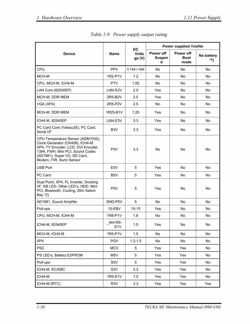
The power supply output rating is specified in Table 1-9.
TECRA M1 Maintenance Manual (960-436) 1-29
1 Hardware Overview 1.11 Power Supply
Table 1-9 Power supply output rating
Power supplied Yes/No
Device Name DC Voltage (V)
Power off Suspen
d
Power off Boot mode
No battery *1)
CPU PPV 0.748-1.468 No No No
MCH-M 1R2-P1V 1.2 No No No
CPU, MCH-M, ICH4-M PTV 1.05 No No No
LAN Cont (82540EP) LAN-E2V 2.5 Yes No No
MCH-M, DDR MEM 2R5-B2V 2.5 Yes No No
VGA (XP4) 2R5-P2V 2.5 No No No
MCH-M, DDR MEM 1R25-B1V 1.25 Yes No No
ICH4-M, 82540EP LAN-E3V 3.3 Yes No No
PC Card Cont (Yebisu3S), PC Card, Serial I/F B3V 3.3 Yes No No
CPU Temperature Sensor (ADM1032), Clock Generator (CK408), ICH4-M, XP4, TV Encoder, LCD, DVI Encoder, 1394, FWH, Mini PCI, Sound Codec (AD1981), Super I/O, SD Card, Modem, FIR, Illumi Sensor
P3V 3.3 No No No
USB Port E5V 5 Yes No No
PC Card B5V 5 Yes No No
Dual Point, XP4, FL Inverter, Docking I/F, KB LED, Other LED’s, HDD, Mini PCI, Bluetooth, Cooling, Slim Select Bay *2)
P5V 5 Yes No No
AD1981, Sound Amplifer SND-P5V 5 No No No
Pull-ups 15-EBV 10-15 Yes No No
CPU, MCH-M, ICH4-M 1R8-P1V 1.8 No No No
ICH4-M, 82540EP _AN1R5-E1V 1.5 Yes No No
MCH-M, ICH4-M 1R5-P1V 1.5 No No No
XP4 PGV 1.2-1.5 No No No
PSC MCV 5 Yes Yes No
PS LED’s, Battery E2PROM M5V 5 Yes Yes No
Pull-ups S5V 5 Yes Yes No
ICH4-M, EC/KBC S3V 3.3 Yes Yes No
ICH4-M 1R5-S1V 1.5 Yes Yes No
ICH4-M (RTC) R3V 3.3 Yes Yes Yes
1-30 TECRA M1 Maintenance Manual (960-436)
1.11 Power Supply 1 Hardware Overview
*1) Both Main battery and Sub Battery are empty, and only RTC Battery is charged.
*2) CD-ROM or DVD-ROM drive Unit is attached.
TECRA M1 Maintenance Manual (960-436) 1-31
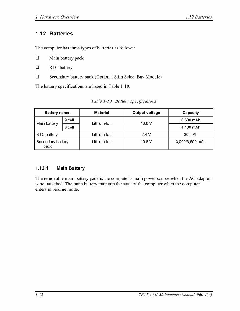
1 Hardware Overview 1.12 Batteries
1.12 Batteries
The computer has three types of batteries as follows:
Main battery pack
RTC battery
Secondary battery pack (Optional Slim Select Bay Module)
The battery specifications are listed in Table 1-10.
Table 1-10 Battery specifications
Battery name Material Output voltage Capacity
9 cell 6,600 mAh Main battery
6 cell Lithium-Ion 10.8 V
4,400 mAh
RTC battery Lithium-Ion 2.4 V 30 mAh
Secondary battery pack
Lithium-Ion 10.8 V 3,000/3,600 mAh
1.12.1 Main Battery
The removable main battery pack is the computer’s main power source when the AC adaptor is not attached. The main battery maintain the state of the computer when the computer enters in resume mode.
1-32 TECRA M1 Maintenance Manual (960-436)
1.12 Batteries 1 Hardware Overview
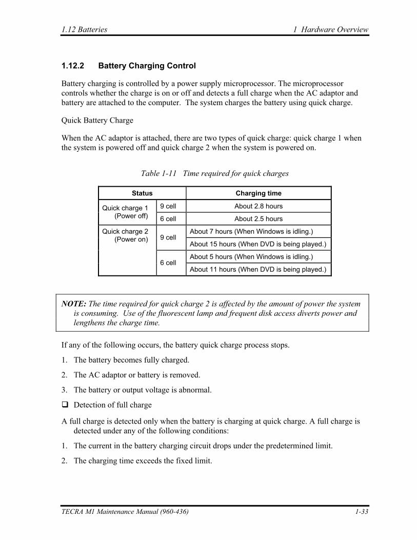
1.12.2 Battery Charging Control
Battery charging is controlled by a power supply microprocessor. The microprocessor controls whether the charge is on or off and detects a full charge when the AC adaptor and battery are attached to the computer. The system charges the battery using quick charge.
Quick Battery Charge
When the AC adaptor is attached, there are two types of quick charge: quick charge 1 when the system is powered off and quick charge 2 when the system is powered on.
Table 1-11 Time required for quick charges
Status Charging time
9 cell About 2.8 hours Quick charge 1 (Power off) 6 cell About 2.5 hours
About 7 hours (When Windows is idling.) 9 cell
About 15 hours (When DVD is being played.)
About 5 hours (When Windows is idling.)
Quick charge 2 (Power on)
6 cell About 11 hours (When DVD is being played.)
NOTE: The time required for quick charge 2 is affected by the amount of power the system is consuming. Use of the fluorescent lamp and frequent disk access diverts power and lengthens the charge time.
If any of the following occurs, the battery quick charge process stops.
1. The battery becomes fully charged.
2. The AC adaptor or battery is removed.
3. The battery or output voltage is abnormal.
Detection of full charge
A full charge is detected only when the battery is charging at quick charge. A full charge is detected under any of the following conditions:
1. The current in the battery charging circuit drops under the predetermined limit.
2. The charging time exceeds the fixed limit.
TECRA M1 Maintenance Manual (960-436) 1-33
1 Hardware Overview 1.12 Batteries
1-34 TECRA M1 Maintenance Manual (960-436)
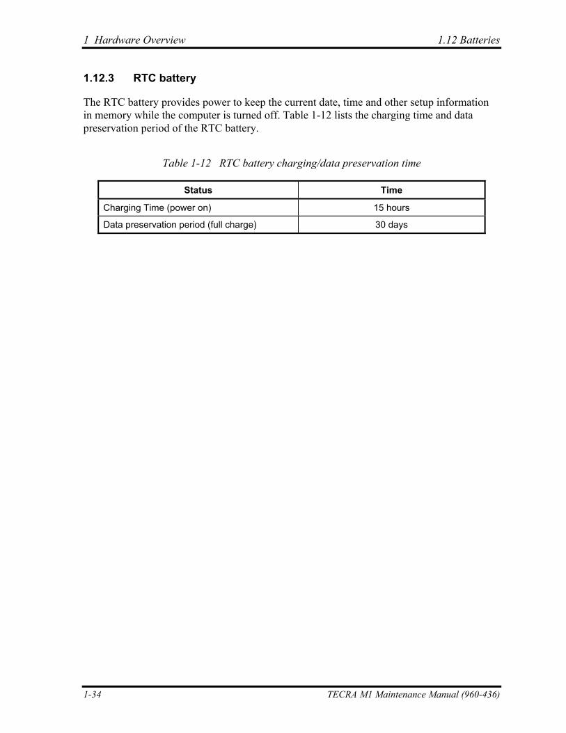
1.12.3 RTC battery
The RTC battery provides power to keep the current date, time and other setup information in memory while the computer is turned off. Table 1-12 lists the charging time and data preservation period of the RTC battery.
Table 1-12 RTC battery charging/data preservation time
Status Time
Charging Time (power on) 15 hours
Data preservation period (full charge) 30 days
Chapter 2 Troubleshooting Procedures
2 Troubleshooting Procedures
2-ii TECRA M1 Maintenance Manual (960-436)
2 Troubleshooting Procedures
Chapter 2 Contents
2.1 Troubleshooting......................................................................................................... 2-1
2.2 Troubleshooting Flowchart ....................................................................................... 2-2
2.3 Power Supply Troubleshooting ................................................................................. 2-6
Procedure 1 Icons in the LCD Check.............................................................. 2-6
Procedure 2 Error Code Check ....................................................................... 2-7
Procedure 3 Connection Check..................................................................... 2-13
Procedure 4 Charge Check............................................................................ 2-14
Procedure 5 Replacement Check................................................................... 2-15
2.4 System Board Troubleshooting ............................................................................... 2-16
Procedure 1 Message Check ......................................................................... 2-17
Procedure 2 Printer Port LED Check on Boot Mode.................................... 2-19
Procedure 3 Diagnostic Test Program Execution Check .............................. 2-28
Procedure 4 Replacement Check................................................................... 2-29
2.5 FDD Troubleshooting.............................................................................................. 2-30
Procedure 1 FDD Head Cleaning Check....................................................... 2-30
Procedure 2 Diagnostic Test Program Execution Check .............................. 2-31
Procedure 3 Connector Check and Replacement Check............................... 2-32
2.6 HDD Troubleshooting ............................................................................................. 2-33
Procedure 1 Message Check ......................................................................... 2-33
Procedure 2 Partition Check.......................................................................... 2-34
Procedure 3 Format Check............................................................................ 2-35
Procedure 4 Diagnostic Test Program Execution Check .............................. 2-36
Procedure 5 Connector Check and Replacement Check............................... 2-37
2.7 Keyboard and Touch pad Troubleshooting ............................................................. 2-38
Procedure 1 Diagnostic Test Program Execution Check .............................. 2-38
Procedure 2 Connector and Replacement Check .......................................... 2-39
2.8 Display Troubleshooting ......................................................................................... 2-41
Procedure 1 Diagnostic Test Program Execution Check .............................. 2-41
Procedure 2 Connector and Cable Check...................................................... 2-41
Procedure 3 Replacement Check................................................................... 2-42
TECRA M1 Maintenance Manual (960-436) 2-iii
2 Troubleshooting Procedures
2.9 CD-ROM Drive Troubleshooting............................................................................ 2-43
Procedure 1 Diagnostic Test Program Execution Check .............................. 2-43
Procedure 2 Connector Check and Replacement Check............................... 2-44
2.10 DVD-ROM, CD-RW/DVD-ROM and DVD Multi Drive Troubleshooting........... 2-45
Procedure 1 Diagnostic Test Program Execution Check .............................. 2-45
Procedure 2 Connector Check and Replacement Check............................... 2-46
2.11 Modem Troubleshooting ......................................................................................... 2-47
Procedure 1 Diagnostic Test Program Execution Check .............................. 2-47
Procedure 2 Connector Check and Replacement Check............................... 2-48
2.12 LAN Troubleshooting ............................................................................................. 2-49
Procedure 1 Connector Check and Replacement Check............................... 2-49
2.13 Bluetooth Troubleshooting...................................................................................... 2-50
Procedure 1 Transmitting-Receiving Check ................................................. 2-50
Procedure 2 Antennas' Connection Check .................................................... 2-51
Procedure 3 Antenna Check.......................................................................... 2-52
Procedure 4 Replacement Check................................................................... 2-53
2.14 Wireless LAN Troubleshooting .............................................................................. 2-54
Procedure 1 Transmitting-Receiving Check ................................................. 2-54
Procedure 2 Antennas' Connection Check .................................................... 2-55
Procedure 3 Antenna Check.......................................................................... 2-56
Procedure 4 Replacement Check................................................................... 2-57
2.15 Sound Troubleshooting ........................................................................................... 2-58
Procedure 1 Diagnostic Test Program Execution Check .............................. 2-58
Procedure 2 Connector Check....................................................................... 2-59
Procedure 3 Replacement Check................................................................... 2-60
2.16 SD Card Slot Troubleshooting ................................................................................ 2-61
Procedure 1 Check on Windows ................................................................... 2-61
Procedure 2 Connector/Replacement Check................................................. 2-61
2-iv TECRA M1 Maintenance Manual (960-436)
2 Troubleshooting Procedures
Figures
Figure 2-1 Troubleshooting flowchart................................................................................. 2-3
Figure 2-2 Printer port LED .............................................................................................. 2-19
Figure 2-3 Antenna Test cable .......................................................................................... 2-52
Figure 2-4 Antenna Test cable .......................................................................................... 2-56
Tables
Table 2-1 Battery Icon.......................................................................................................... 2-6
Table 2-2 DC IN Icon........................................................................................................... 2-6
Table 2-3 Printer port LED boot mode status .................................................................... 2-20
Table 2-4 FDD error code and status ................................................................................. 2-31
Table 2-5 Hard disk drive error code and status ................................................................ 2-36
TECRA M1 Maintenance Manual (960-436) 2-v

2 Troubleshooting Procedures
2-vi TECRA M1 Maintenance Manual (960-436)
2.1 Troubleshooting 2 Troubleshooting Procedures
2
2.1 Troubleshooting
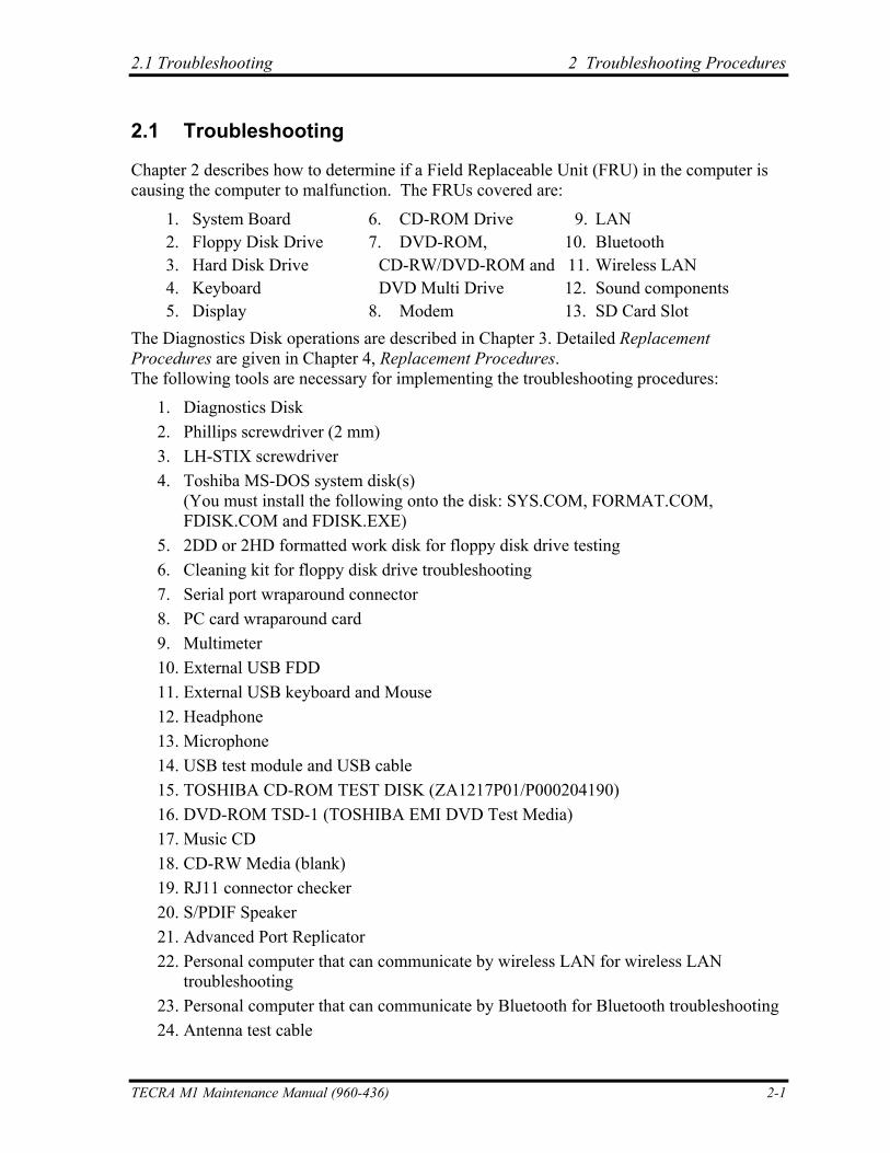
Chapter 2 describes how to determine if a Field Replaceable Unit (FRU) in the computer is causing the computer to malfunction. The FRUs covered are:
1. System Board 6. CD-ROM Drive 9. LAN 2. Floppy Disk Drive 7. DVD-ROM, 10. Bluetooth 3. Hard Disk Drive CD-RW/DVD-ROM and 11. Wireless LAN 4. Keyboard DVD Multi Drive 12. Sound components 5. Display 8. Modem 13. SD Card Slot The Diagnostics Disk operations are described in Chapter 3. Detailed Replacement Procedures are given in Chapter 4, Replacement Procedures. The following tools are necessary for implementing the troubleshooting procedures:
1. Diagnostics Disk 2. Phillips screwdriver (2 mm) 3. LH-STIX screwdriver 4. Toshiba MS-DOS system disk(s)
(You must install the following onto the disk: SYS.COM, FORMAT.COM, FDISK.COM and FDISK.EXE)
5. 2DD or 2HD formatted work disk for floppy disk drive testing 6. Cleaning kit for floppy disk drive troubleshooting 7. Serial port wraparound connector 8. PC card wraparound card 9. Multimeter 10. External USB FDD 11. External USB keyboard and Mouse 12. Headphone 13. Microphone 14. USB test module and USB cable 15. TOSHIBA CD-ROM TEST DISK (ZA1217P01/P000204190) 16. DVD-ROM TSD-1 (TOSHIBA EMI DVD Test Media) 17. Music CD 18. CD-RW Media (blank) 19. RJ11 connector checker 20. S/PDIF Speaker 21. Advanced Port Replicator 22. Personal computer that can communicate by wireless LAN for wireless LAN
troubleshooting 23. Personal computer that can communicate by Bluetooth for Bluetooth troubleshooting 24. Antenna test cable
TECRA M1 Maintenance Manual (960-436) 2-1
2 Troubleshooting Procedures 2.2 Troubleshooting Flowchart
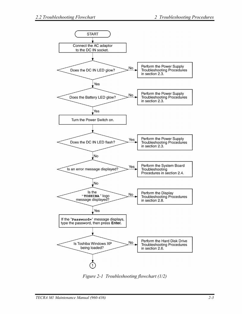
2.2 Troubleshooting Flowchart
Use the flowchart in figure 2-1 as a guide for determining which troubleshooting procedures to execute. Before going through the flowchart steps, verify the following:
Ask the user if a password is registered and, if it is, ask him or her to enter the password. If the user has forgotten the system password, perform the following procedure at the appropriate step in the flowchart in figure 2-1:
Connect the printer port in the Port Replicator, hold down the “P” key and turn the POWER switch on. The computer will override the password function by erasing the current password.
Verify with the customer that Microsoft Windows is installed on the hard disk. Non-Windows operating systems can cause the computer to malfunction.
Make sure all optional equipment is removed from the computer.
Make sure the External USB floppy disk drive is empty.
2-2 TECRA M1 Maintenance Manual (960-436)
2.2 Troubleshooting Flowchart 2 Troubleshooting Procedures
Figure 2-1 Troubleshooting flowchart (1/2)
TECRA M1 Maintenance Manual (960-436) 2-3
2 Troubleshooting Procedures 2.2 Troubleshooting Flowchart
Keyboard/Touch pad
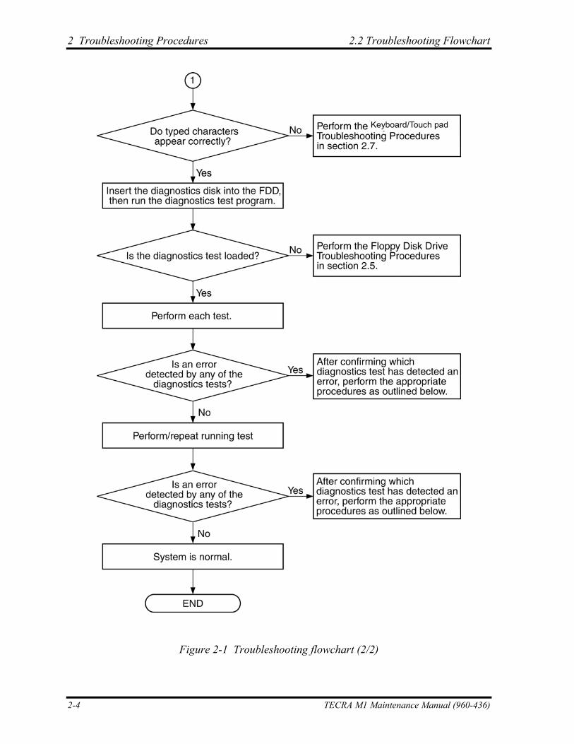
Figure 2-1 Troubleshooting flowchart (2/2)
2-4 TECRA M1 Maintenance Manual (960-436)
2.2 Troubleshooting Flowchart 2 Troubleshooting Procedures
If the diagnostics program cannot detect an error, the problem may be intermittent. The Running Test program should be executed several times to isolate the problem. Check the Log Utilities function to confirm which diagnostic test detected an error, then perform the appropriate troubleshooting procedures as follows:
1. If an error is detected on the system test, memory test, real timer test, perform the System Board Troubleshooting Procedures in Section 2.4.
2. If an error is detected on the floppy disk test, perform the FDD Troubleshooting Procedures in Section 2.5.
3. If an error is detected on the hard disk test, perform the HDD Troubleshooting Procedures in Section 2.6.
4. If an error is detected on the keyboard test, perform the Keyboard and Touch pad Troubleshooting Procedures in Section 2.7.
5. If an error is detected on the display test, perform the Display Troubleshooting Procedures in Section 2.8.
6. If an error is detected on the CD-ROM test, perform the CD-ROM Drive Troubleshooting Procedures in Section 2.9.
7. If an error is detected on the DVD-ROM, CD-RW/DVD-ROM or DVD Multi Drive test, perform the DVD-ROM, CD-RW/DVD-ROM and DVD Multi Drive Troubleshooting Procedures in Section 2.10.
8. If an error is detected on the modem test, perform the Modem Troubleshooting Procedures in Section 2.11.
9. If an error is detected on the Bluetooth test, perform the Bluetooth Troubleshooting Procedures in Section 2.13.
10. If an error is detected on the Wireless LAN test, perform the Wireless LAN Troubleshooting Procedures in Section 2.14.
11. If an error is detected on the sound test, perform the Sound Troubleshooting Procedures in Section 2.15.
12. If an error is detected on the SD card slot test, perform the SD Card Slot Troubleshooting in Section 2.16.
TECRA M1 Maintenance Manual (960-436) 2-5
2 Troubleshooting Procedures 2.3 Power Supply Troubleshooting
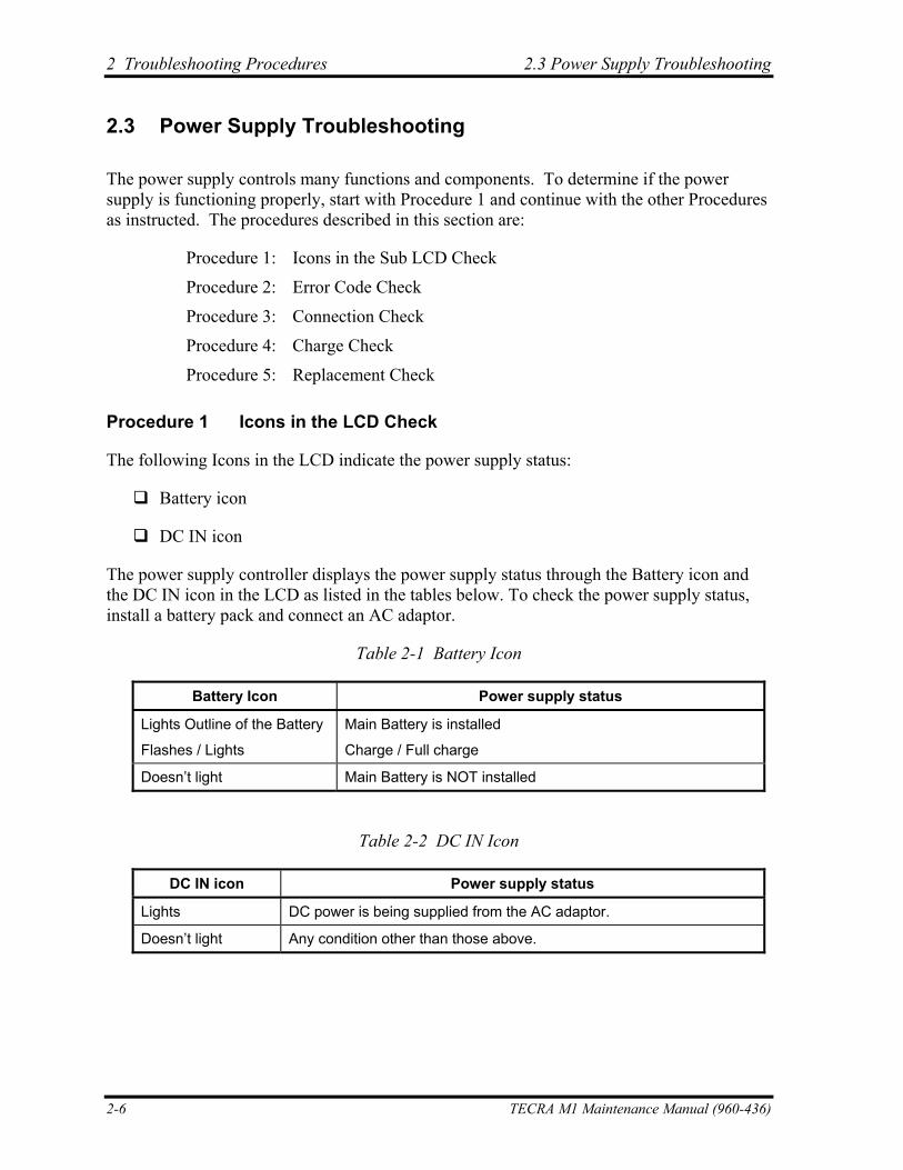
2.3 Power Supply Troubleshooting
The power supply controls many functions and components. To determine if the power supply is functioning properly, start with Procedure 1 and continue with the other Procedures as instructed. The procedures described in this section are:
Procedure 1: Icons in the Sub LCD Check
Procedure 2: Error Code Check
Procedure 3: Connection Check
Procedure 4: Charge Check
Procedure 5: Replacement Check
Procedure 1 Icons in the LCD Check
The following Icons in the LCD indicate the power supply status:
Battery icon
DC IN icon
The power supply controller displays the power supply status through the Battery icon and the DC IN icon in the LCD as listed in the tables below. To check the power supply status, install a battery pack and connect an AC adaptor.
Table 2-1 Battery Icon
Battery Icon Power supply status
Lights Outline of the Battery
Flashes / Lights
Main Battery is installed
Charge / Full charge
Doesn’t light Main Battery is NOT installed
Table 2-2 DC IN Icon
DC IN icon Power supply status
Lights DC power is being supplied from the AC adaptor.
Doesn’t light Any condition other than those above.
2-6 TECRA M1 Maintenance Manual (960-436)
2.3 Power Supply Troubleshooting 2 Troubleshooting Procedures
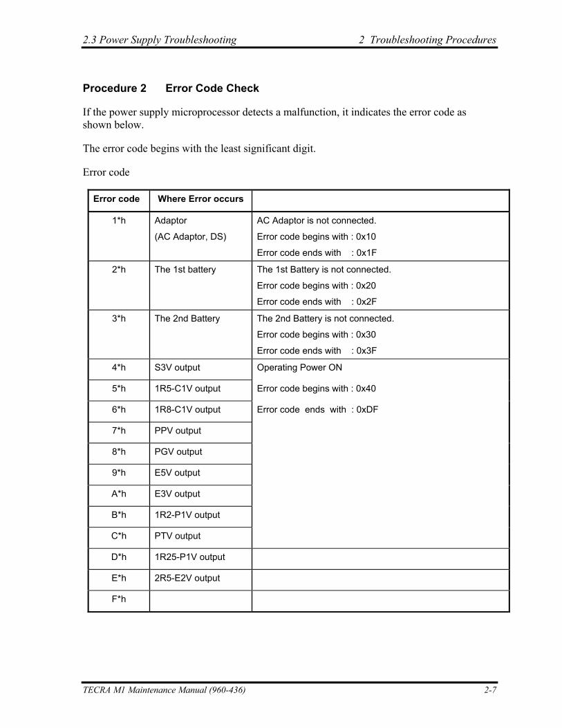
Procedure 2 Error Code Check
If the power supply microprocessor detects a malfunction, it indicates the error code as shown below.
The error code begins with the least significant digit.
Error code
Error code Where Error occurs
1*h Adaptor
(AC Adaptor, DS)
AC Adaptor is not connected.
Error code begins with : 0x10
Error code ends with : 0x1F
2*h The 1st battery The 1st Battery is not connected.
Error code begins with : 0x20
Error code ends with : 0x2F
3*h The 2nd Battery The 2nd Battery is not connected.
Error code begins with : 0x30
Error code ends with : 0x3F
4*h S3V output Operating Power ON
5*h 1R5-C1V output Error code begins with : 0x40
6*h 1R8-C1V output Error code ends with : 0xDF
7*h PPV output
8*h PGV output
9*h E5V output
A*h E3V output
B*h 1R2-P1V output
C*h PTV output
D*h 1R25-P1V output
E*h 2R5-E2V output
F*h
TECRA M1 Maintenance Manual (960-436) 2-7
2 Troubleshooting Procedures 2.3 Power Supply Troubleshooting
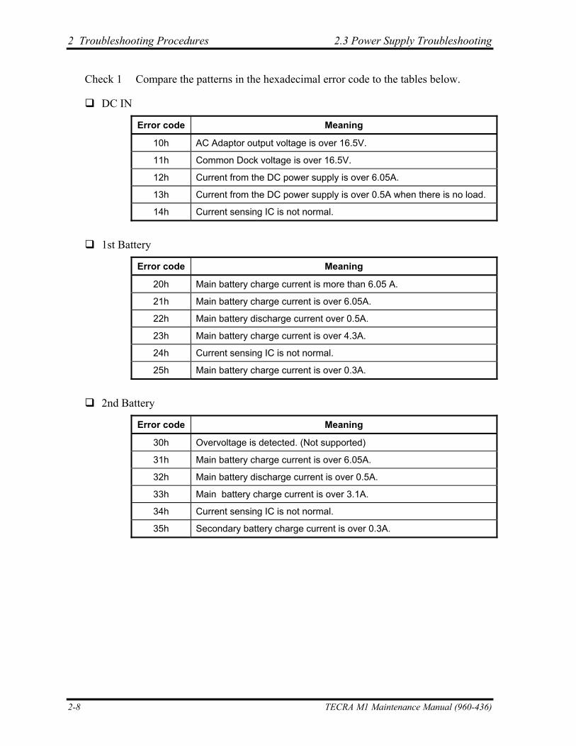
Check 1 Compare the patterns in the hexadecimal error code to the tables below.
DC IN
Error code Meaning
10h AC Adaptor output voltage is over 16.5V.
11h Common Dock voltage is over 16.5V.
12h Current from the DC power supply is over 6.05A.
13h Current from the DC power supply is over 0.5A when there is no load.
14h Current sensing IC is not normal.
1st Battery
Error code Meaning
20h Main battery charge current is more than 6.05 A.
21h Main battery charge current is over 6.05A.
22h Main battery discharge current over 0.5A.
23h Main battery charge current is over 4.3A.
24h Current sensing IC is not normal.
25h Main battery charge current is over 0.3A.
2nd Battery
Error code Meaning
30h Overvoltage is detected. (Not supported)
31h Main battery charge current is over 6.05A.
32h Main battery discharge current is over 0.5A.
33h Main battery charge current is over 3.1A.
34h Current sensing IC is not normal.
35h Secondary battery charge current is over 0.3A.
2-8 TECRA M1 Maintenance Manual (960-436)
2.3 Power Supply Troubleshooting 2 Troubleshooting Procedures
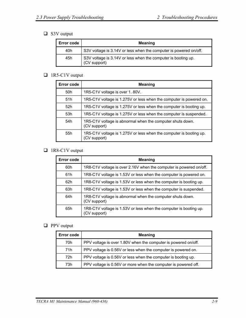
S3V output
Error code Meaning
40h S3V voltage is 3.14V or less when the computer is powered on/off.
45h S3V voltage is 3.14V or less when the computer is booting up. (CV support)
1R5-C1V output
Error code Meaning
50h 1R5-C1V voltage is over 1. 80V.
51h 1R5-C1V voltage is 1.275V or less when the computer is powered on.
52h 1R5-C1V voltage is 1.275V or less when the computer is booting up.
53h 1R5-C1V voltage is 1.275V or less when the computer is suspended.
54h 1R5-C1V voltage is abnormal when the computer shuts down. (CV support)
55h 1R5-C1V voltage is 1.275V or less when the computer is booting up. (CV support)
1R8-C1V output
Error code Meaning
60h 1R8-C1V voltage is over 2.16V when the computer is powered on/off.
61h 1R8-C1V voltage is 1.53V or less when the computer is powered on.
62h 1R8-C1V voltage is 1.53V or less when the computer is booting up.
63h 1R8-C1V voltage is 1.53V or less when the computer is suspended.
64h 1R8-C1V voltage is abnormal when the computer shuts down. (CV support)
65h 1R8-C1V voltage is 1.53V or less when the computer is booting up. (CV support)
PPV output
Error code Meaning
70h PPV voltage is over 1.80V when the computer is powered on/off.
71h PPV voltage is 0.56V or less when the computer is powered on.
72h PPV voltage is 0.56V or less when the computer is booting up.
73h PPV voltage is 0.56V or more when the computer is powered off.
TECRA M1 Maintenance Manual (960-436) 2-9
2 Troubleshooting Procedures 2.3 Power Supply Troubleshooting
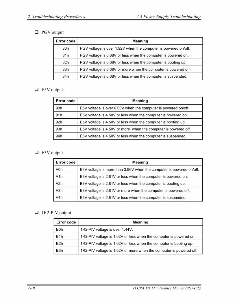
PGV output
Error code Meaning
80h PGV voltage is over 1.92V when the computer is powered on/off.
81h PGV voltage is 0.68V or less when the computer is powered on.
82h PGV voltage is 0.68V or less when the computer is booting up.
83h PGV voltage is 0.68V or more when the computer is powered off.
84h PGV voltage is 0.68V or less when the computer is suspended.
E5V output
Error code Meaning
90h E5V voltage is over 6.00V when the computer is powered on/off.
91h E5V voltage is 4.50V or less when the computer is powered on.
92h E5V voltage is 4.50V or less when the computer is booting up.
93h E5V voltage is 4.50V or more when the computer is powered off.
94h E5V voltage is 4.50V or less when the computer is suspended.
E3V output
Error code Meaning
A0h E3V voltage is more than 3.96V when the computer is powered on/off.
A1h E3V voltage is 2.81V or less when the computer is powered on.
A2h E3V voltage is 2.81V or less when the computer is booting up.
A3h E3V voltage is 2.81V or more when the computer is powered off.
A4h E3V voltage is 2.81V or less when the computer is suspended.
1R2-PIV output
Error code Meaning
B0h 1R2-PIV voltage is over 1.44V.
B1h 1R2-PIV voltage is 1.02V or less when the computer is powered on.
B2h 1R2-PIV voltage is 1.02V or less when the computer is booting up.
B3h 1R2-PIV voltage is 1.02V or more when the computer is powered off.
2-10 TECRA M1 Maintenance Manual (960-436)
2.3 Power Supply Troubleshooting 2 Troubleshooting Procedures
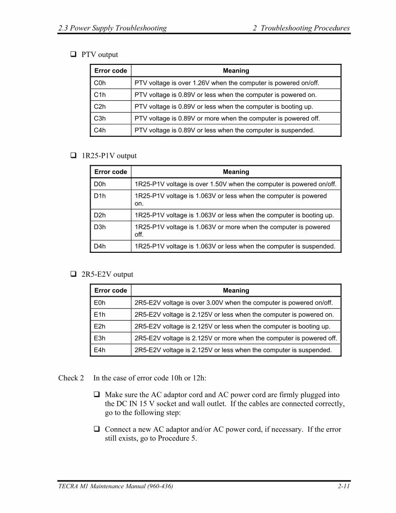
PTV output
Error code Meaning
C0h PTV voltage is over 1.26V when the computer is powered on/off.
C1h PTV voltage is 0.89V or less when the computer is powered on.
C2h PTV voltage is 0.89V or less when the computer is booting up.
C3h PTV voltage is 0.89V or more when the computer is powered off.
C4h PTV voltage is 0.89V or less when the computer is suspended.
1R25-P1V output
Error code Meaning
D0h 1R25-P1V voltage is over 1.50V when the computer is powered on/off.
D1h 1R25-P1V voltage is 1.063V or less when the computer is powered on.
D2h 1R25-P1V voltage is 1.063V or less when the computer is booting up.
D3h 1R25-P1V voltage is 1.063V or more when the computer is powered off.
D4h 1R25-P1V voltage is 1.063V or less when the computer is suspended.
2R5-E2V output
Error code Meaning
E0h 2R5-E2V voltage is over 3.00V when the computer is powered on/off.
E1h 2R5-E2V voltage is 2.125V or less when the computer is powered on.
E2h 2R5-E2V voltage is 2.125V or less when the computer is booting up.
E3h 2R5-E2V voltage is 2.125V or more when the computer is powered off.
E4h 2R5-E2V voltage is 2.125V or less when the computer is suspended.
Check 2 In the case of error code 10h or 12h:
Make sure the AC adaptor cord and AC power cord are firmly plugged into the DC IN 15 V socket and wall outlet. If the cables are connected correctly, go to the following step:
Connect a new AC adaptor and/or AC power cord, if necessary. If the error still exists, go to Procedure 5.
TECRA M1 Maintenance Manual (960-436) 2-11
2 Troubleshooting Procedures 2.3 Power Supply Troubleshooting
Check 3 In the case of error code 2Xh:
Make sure the battery pack is correctly installed in the computer. If the battery pack is correctly installed, go to the following step:
Replace the battery pack with a new one. If the error still exists, go to Procedure 5.
Check 4 For any other error, go to Procedure 5.
2-12 TECRA M1 Maintenance Manual (960-436)
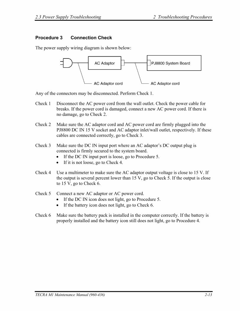
2.3 Power Supply Troubleshooting 2 Troubleshooting Procedures
Procedure 3 Connection Check
The power supply wiring diagram is shown below:
Any of the connectors may be disconnected. Perform Check 1.
Check 1 Disconnect the AC power cord from the wall outlet. Check the power cable for breaks. If the power cord is damaged, connect a new AC power cord. If there is no damage, go to Check 2.
Check 2 Make sure the AC adaptor cord and AC power cord are firmly plugged into the PJ8800 DC IN 15 V socket and AC adaptor inlet/wall outlet, respectively. If these cables are connected correctly, go to Check 3.
Check 3 Make sure the DC IN input port where an AC adaptor’s DC output plug is connected is firmly secured to the system board. • If the DC IN input port is loose, go to Procedure 5. • If it is not loose, go to Check 4.
Check 4 Use a multimeter to make sure the AC adaptor output voltage is close to 15 V. If the output is several percent lower than 15 V, go to Check 5. If the output is close to 15 V, go to Check 6.
Check 5 Connect a new AC adaptor or AC power cord. • If the DC IN icon does not light, go to Procedure 5. • If the battery icon does not light, go to Check 6.
Check 6 Make sure the battery pack is installed in the computer correctly. If the battery is properly installed and the battery icon still does not light, go to Procedure 4.
TECRA M1 Maintenance Manual (960-436) 2-13
2 Troubleshooting Procedures 2.3 Power Supply Troubleshooting
Procedure 4 Charge Check
The power supply may not charge the battery pack. Perform the following procedures:
1. Reinstall the battery pack.
2. Attach the AC adaptor and turn on the power. If you cannot turn on the power, go to Procedure 5.
3. Run the Diagnostic test, go to System test and execute subtest 06 (Quick charge) described in Chapter 3.
4. When charge is complete, the diagnostics test displays the result code. Check the result code against the table below and perform any necessary check.
Result code Contents Check items
0 The battery is charging normally. Normal
1 The battery is fully charged. Normal
2 The AC adaptor is not attached. Check 1
3 The AC adaptor’s output voltage is not normal. Check 1
4 The battery is not installed. Check 2
5 The battery’s output voltage is not normal. Check 3
6 The battery’s temperature is not normal. Check 4
7 A bad battery is installed. Check 2
8 Any other problems. Check 5
Check 1 Make sure the AC adaptor and AC power cord are firmly plugged into the DC IN socket and the wall outlet. If these cables are connected correctly, replace the AC adaptor (and/or AC power cord, if necessary).
Check 2 Make sure the battery is properly installed. If the battery is properly installed, go to Check 3.
Check 3 The battery pack may be completely discharged. Wait a few minutes to charge the battery pack. If the battery pack is still not charged, go to Check 4.
Check 4 The battery’s temperature is too hot or cold. Return the temperature to a normal operating condition. If the battery pack still is not charged, go to Check 5.
Check 5 Replace the battery pack with a new one. If the battery pack still is not charged, go to Procedure 5.
2-14 TECRA M1 Maintenance Manual (960-436)
2.3 Power Supply Troubleshooting 2 Troubleshooting Procedures
Procedure 5 Replacement Check
The system board processor module may be disconnected or damaged. Disassemble the computer following the steps described in Chapter 4, Replacement Procedures. Check the connection between the AC adaptor and system board and connection. After checking the connections, perform the following Check 1:
Check 1 Replace the AC adaptor with a new one. If the AC adaptor is still not functioning properly, perform Check 2.
Check 2 Use a multimeter to make sure that the F800, F810 and F820 fuse are not blown. If fuses are not blown, go to Check 3.
Check 3 Replace the system board with a new one following the steps described in Chapter 4, Replacement Procedures.
TECRA M1 Maintenance Manual (960-436) 2-15
2 Troubleshooting Procedures 2.5 FDD TroubleshootingSystem Board Troubleshooting
2.4 System Board Troubleshooting
This section describes how to determine if the system board and CPU are defective or not functioning properly. Start with Procedure 1 and continue with the other procedures as instructed.
The procedures described in this section are:
Procedure 1: Message Check
Procedure 2: Printer Port LED Check on Resume Mode
Procedure 3: Diagnostic Test Program Execution Check
Procedure 4: Replacement Check
2-16 TECRA M1 Maintenance Manual (960-436)
2.4 System Board Troubleshooting 2 Troubleshooting Procedures
Procedure 1 Message Check
When the power is turned on, the system performs the Initial Reliability Test (IRT) installed in the BIOS ROM. The IRT tests each IC on the system board and initializes it.
If an error message is shown on the display, perform Check 1.
If there is no error message, go to Procedure 2.
If Toshiba MS-DOS or Windows Me is properly loaded, go to Procedure 3.
Check 1 If one of the following error messages appears on the screen, press F1 as the message instructs. These errors occur when the system configuration preserved in the RTC memory (CMOS type memory) is not the same as the actual configuration or when the data is lost. If you press F1 as the message instructs, returns all system settings to their default values. Then the system reboots.
If error message (b) appears often when the power is turned on, replace the RTC battery. If any other error message displays, perform Check 2.
(a) *** Bad HDD type *** Check system. Then press [F1] key ......
(b) *** Bad RTC battery *** Check system. Then press [F1] key ......
(c) *** Bad configuration *** Check system. Then press [F1] key ......
(d) *** Bad memory size *** Check system. Then press [F1] key ......
(e) *** Bad time function *** Check system. Then press [F1] key ......
(f) *** Bad check sum (CMOS) *** Check system. Then press [F1] key ......
(g) *** Bad check sum (ROM) *** Check system. Then press [F1] key ......
TECRA M1 Maintenance Manual (960-436) 2-17
2 Troubleshooting Procedures 2.5 FDD TroubleshootingSystem Board Troubleshooting
Check 2 The IRT checks the system board. When the IRT detects an error, the system stops or an error message appears.
If one of the following error messages (1) through (17), (24) or (25) appears, go to Procedure 5.
If the error message (18) appears, go to the Keyboard Troubleshooting Procedures in Section 2.7.
If the error message (19) or (20) appears, go to the HDD Troubleshooting Procedures in Section 2.6.
If the error message (21) appears, go to the CD-R/RW Drive Troubleshooting Procedures in Section 2.9 or the COMBO Drive Troubleshooting Procedures in Section 2.10
If the error message (22) or (23) appears, go to the FDD Troubleshooting Procedures in Section 2.5.
(1) PIT ERROR (2) MEMORY REFRESH ERROR (3) TIMER CH.2 OUT ERROR (4) CMOS CHECKSUM ERROR (5) CMOS BAD BATTERY ERROR (6) FIRST 64KB MEMORY ERROR (7) FIRST 64KB MEMORY PARITY ERROR (8) VRAM ERROR (9) SYSTEM MEMORY ERROR (10) SYSTEM MEMORY PARITY ERROR (11) EXTENDED MEMORY ERROR (12) EXTENDED MEMORY PARITY ERROR (13) DMA PAGE REGISTER ERROR (14) DMAC #1 ERROR (15) DMAC #2 ERROR (16) PIC #1 ERROR (17) PIC #2 ERROR (18) KBC ERROR (19) HDC ERROR (20) IDE #0 ERROR (21) IDE #1 ERROR (22) NO FDD ERROR (23) FDC ERROR (24) TIMER INTERRUPT ERROR (25) RTC UPDATE ERROR
2-18 TECRA M1 Maintenance Manual (960-436)
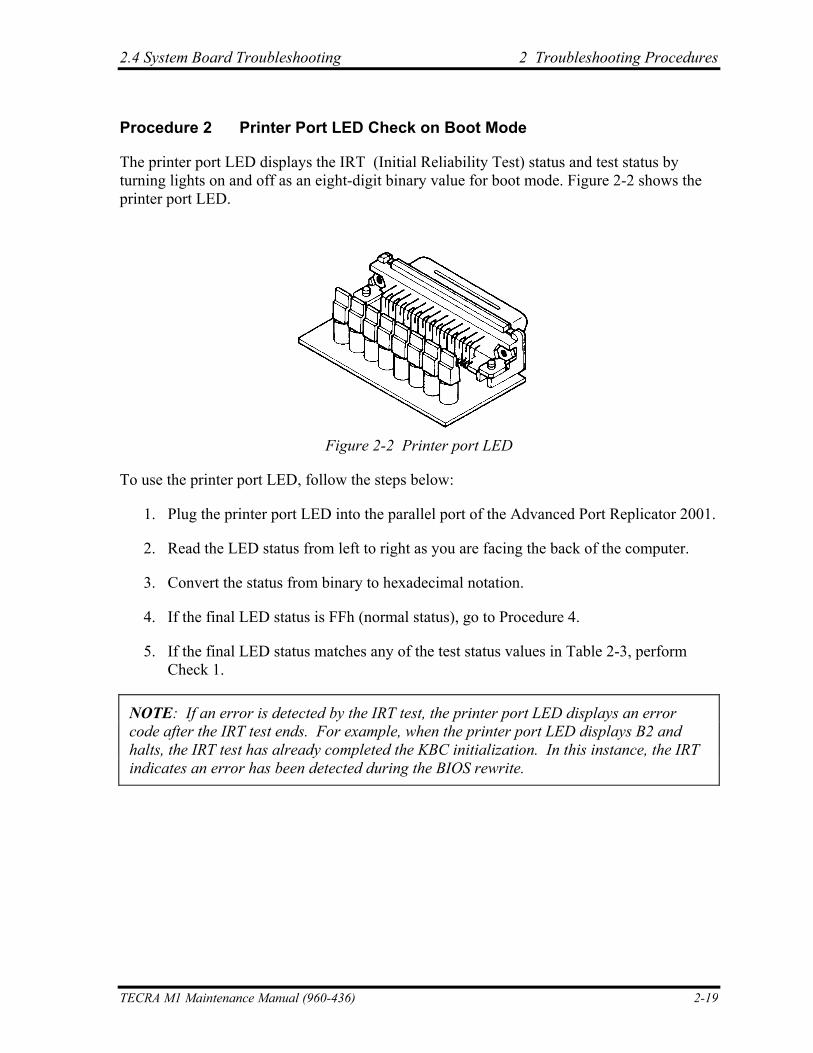
2.4 System Board Troubleshooting 2 Troubleshooting Procedures
Procedure 2 Printer Port LED Check on Boot Mode
The printer port LED displays the IRT (Initial Reliability Test) status and test status by turning lights on and off as an eight-digit binary value for boot mode. Figure 2-2 shows the printer port LED.
Figure 2-2 Printer port LED
To use the printer port LED, follow the steps below:
1. Plug the printer port LED into the parallel port of the Advanced Port Replicator 2001.
2. Read the LED status from left to right as you are facing the back of the computer.
3. Convert the status from binary to hexadecimal notation.
4. If the final LED status is FFh (normal status), go to Procedure 4.
5. If the final LED status matches any of the test status values in Table 2-3, perform Check 1.
NOTE: If an error is detected by the IRT test, the printer port LED displays an error code after the IRT test ends. For example, when the printer port LED displays B2 and halts, the IRT test has already completed the KBC initialization. In this instance, the IRT indicates an error has been detected during the BIOS rewrite.
TECRA M1 Maintenance Manual (960-436) 2-19
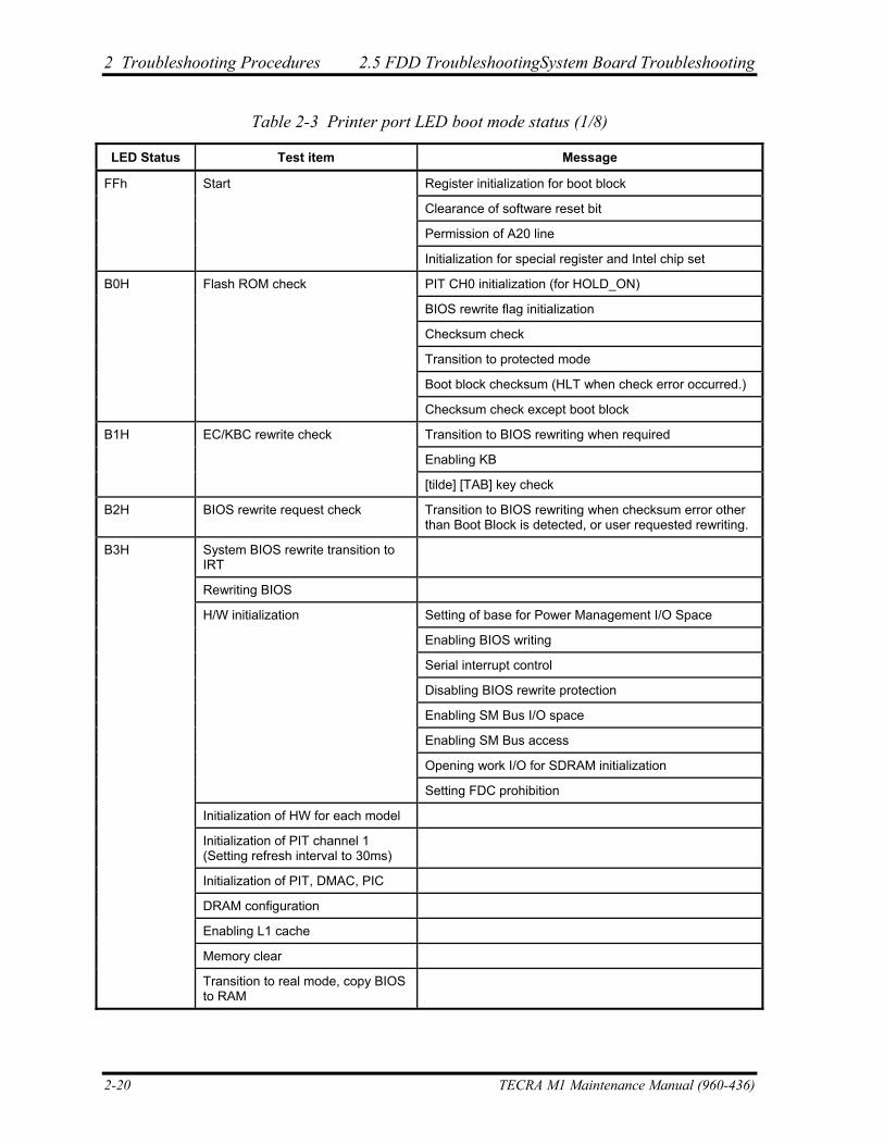
2 Troubleshooting Procedures 2.5 FDD TroubleshootingSystem Board Troubleshooting
Table 2-3 Printer port LED boot mode status (1/8)
LED Status Test item Message
Register initialization for boot block
Clearance of software reset bit
Permission of A20 line
FFh Start
Initialization for special register and Intel chip set
PIT CH0 initialization (for HOLD_ON)
BIOS rewrite flag initialization
Checksum check
Transition to protected mode
Boot block checksum (HLT when check error occurred.)
B0H Flash ROM check
Checksum check except boot block
Transition to BIOS rewriting when required
Enabling KB
B1H EC/KBC rewrite check
[tilde] [TAB] key check
B2H BIOS rewrite request check Transition to BIOS rewriting when checksum error other than Boot Block is detected, or user requested rewriting.
System BIOS rewrite transition to IRT
Rewriting BIOS
Setting of base for Power Management I/O Space
Enabling BIOS writing
Serial interrupt control
Disabling BIOS rewrite protection
Enabling SM Bus I/O space
Enabling SM Bus access
Opening work I/O for SDRAM initialization
H/W initialization
Setting FDC prohibition
Initialization of HW for each model
Initialization of PIT channel 1 (Setting refresh interval to 30ms)
Initialization of PIT, DMAC, PIC
DRAM configuration
Enabling L1 cache
Memory clear
B3H
Transition to real mode, copy BIOS to RAM
2-20 TECRA M1 Maintenance Manual (960-436)
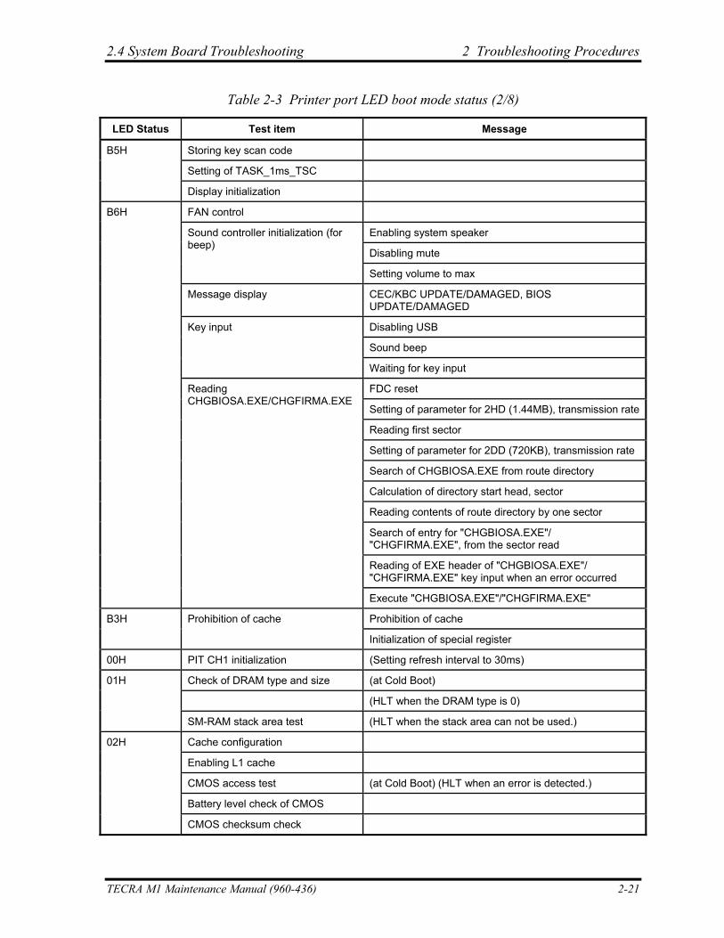
2.4 System Board Troubleshooting 2 Troubleshooting Procedures
Table 2-3 Printer port LED boot mode status (2/8)
LED Status Test item Message
Storing key scan code
Setting of TASK_1ms_TSC
B5H
Display initialization
FAN control
Enabling system speaker
Disabling mute
Sound controller initialization (for beep)
Setting volume to max
Message display CEC/KBC UPDATE/DAMAGED, BIOS UPDATE/DAMAGED
Disabling USB
Sound beep
Key input
Waiting for key input
FDC reset
Setting of parameter for 2HD (1.44MB), transmission rate
Reading first sector
Setting of parameter for 2DD (720KB), transmission rate
Search of CHGBIOSA.EXE from route directory
Calculation of directory start head, sector
Reading contents of route directory by one sector
Search of entry for "CHGBIOSA.EXE"/ "CHGFIRMA.EXE", from the sector read
Reading of EXE header of "CHGBIOSA.EXE"/ "CHGFIRMA.EXE" key input when an error occurred
B6H
Reading CHGBIOSA.EXE/CHGFIRMA.EXE
Execute "CHGBIOSA.EXE"/"CHGFIRMA.EXE"
Prohibition of cache Prohibition of cache B3H
Initialization of special register
00H PIT CH1 initialization (Setting refresh interval to 30ms)
Check of DRAM type and size (at Cold Boot)
(HLT when the DRAM type is 0)
01H
SM-RAM stack area test (HLT when the stack area can not be used.)
Cache configuration
Enabling L1 cache
CMOS access test (at Cold Boot) (HLT when an error is detected.)
Battery level check of CMOS
02H
CMOS checksum check
TECRA M1 Maintenance Manual (960-436) 2-21
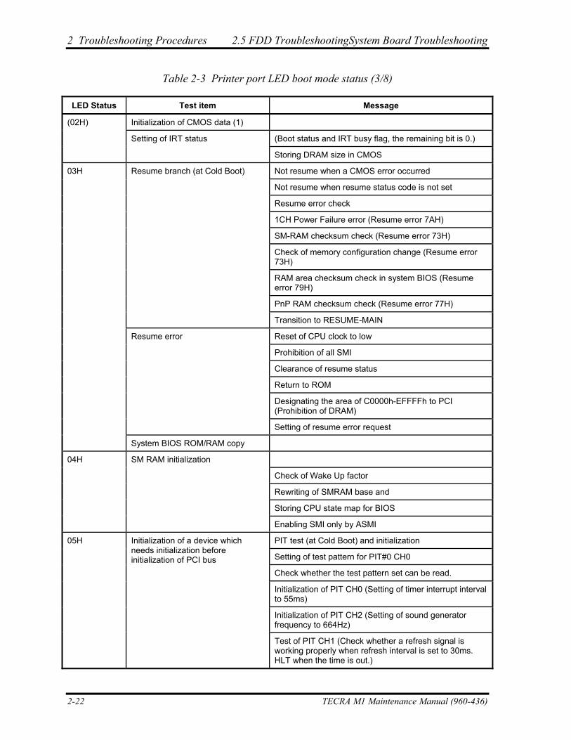
2 Troubleshooting Procedures 2.5 FDD TroubleshootingSystem Board Troubleshooting
Table 2-3 Printer port LED boot mode status (3/8)
LED Status Test item Message
Initialization of CMOS data (1)
(Boot status and IRT busy flag, the remaining bit is 0.)
(02H)
Setting of IRT status
Storing DRAM size in CMOS
Not resume when a CMOS error occurred
Not resume when resume status code is not set
Resume error check
1CH Power Failure error (Resume error 7AH)
SM-RAM checksum check (Resume error 73H)
Check of memory configuration change (Resume error 73H)
RAM area checksum check in system BIOS (Resume error 79H)
PnP RAM checksum check (Resume error 77H)
Resume branch (at Cold Boot)
Transition to RESUME-MAIN
Reset of CPU clock to low
Prohibition of all SMI
Clearance of resume status
Return to ROM
Designating the area of C0000h-EFFFFh to PCI (Prohibition of DRAM)
Resume error
Setting of resume error request
03H
System BIOS ROM/RAM copy
SM RAM initialization
Check of Wake Up factor
Rewriting of SMRAM base and
Storing CPU state map for BIOS
04H
Enabling SMI only by ASMI
PIT test (at Cold Boot) and initialization
Setting of test pattern for PIT#0 CH0
Check whether the test pattern set can be read.
Initialization of PIT CH0 (Setting of timer interrupt interval to 55ms)
Initialization of PIT CH2 (Setting of sound generator frequency to 664Hz)
05H Initialization of a device which needs initialization before initialization of PCI bus
Test of PIT CH1 (Check whether a refresh signal is working properly when refresh interval is set to 30ms. HLT when the time is out.)
2-22 TECRA M1 Maintenance Manual (960-436)
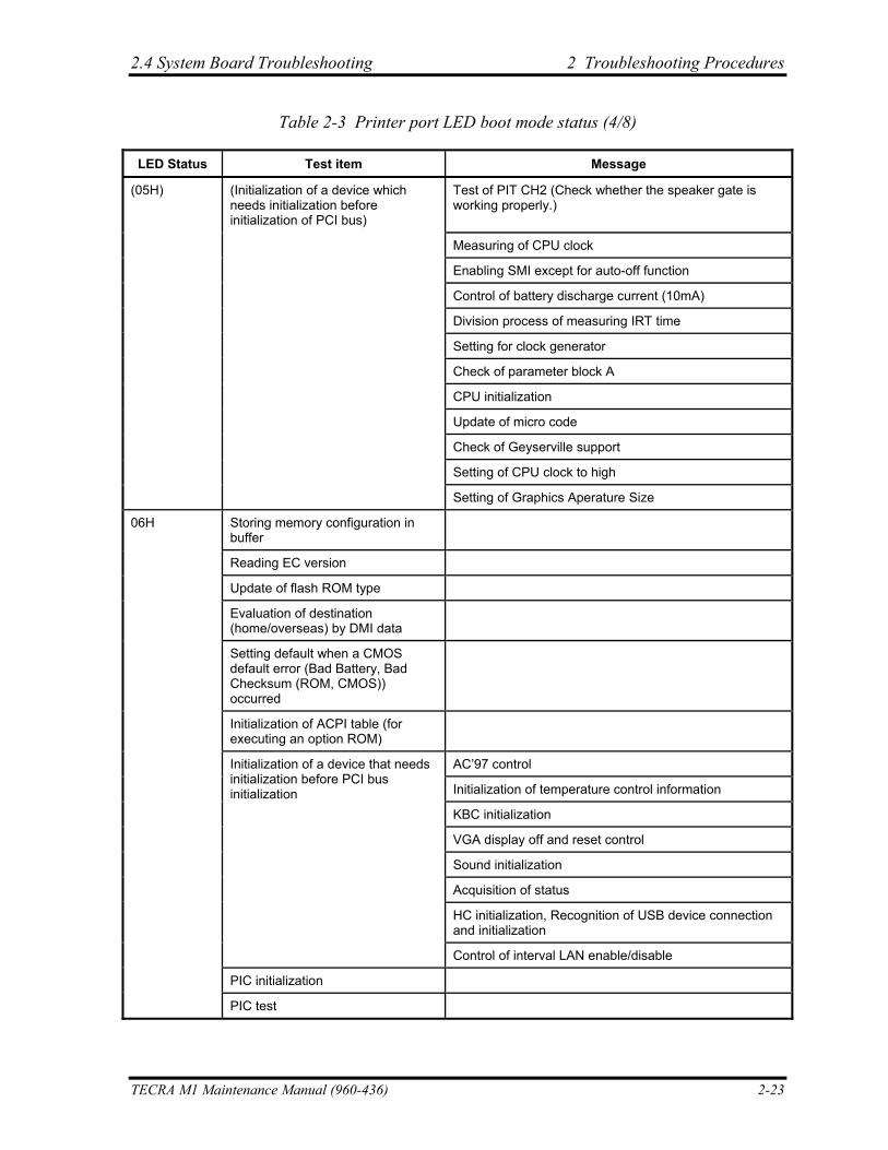
2.4 System Board Troubleshooting 2 Troubleshooting Procedures
Table 2-3 Printer port LED boot mode status (4/8)
LED Status Test item Message
(Initialization of a device which needs initialization before initialization of PCI bus)
Test of PIT CH2 (Check whether the speaker gate is working properly.)
Measuring of CPU clock
Enabling SMI except for auto-off function
Control of battery discharge current (10mA)
Division process of measuring IRT time
Setting for clock generator
Check of parameter block A
CPU initialization
Update of micro code
Check of Geyserville support
Setting of CPU clock to high
(05H)
Setting of Graphics Aperature Size
Storing memory configuration in buffer
Reading EC version
Update of flash ROM type
Evaluation of destination (home/overseas) by DMI data
Setting default when a CMOS default error (Bad Battery, Bad Checksum (ROM, CMOS)) occurred
Initialization of ACPI table (for executing an option ROM)
AC’97 control
Initialization of temperature control information
KBC initialization
VGA display off and reset control
Sound initialization
Acquisition of status
HC initialization, Recognition of USB device connection and initialization
Initialization of a device that needs initialization before PCI bus initialization
Control of interval LAN enable/disable
PIC initialization
06H
PIC test
TECRA M1 Maintenance Manual (960-436) 2-23
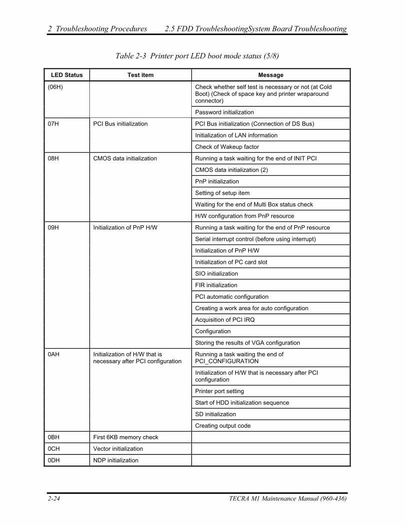
2 Troubleshooting Procedures 2.5 FDD TroubleshootingSystem Board Troubleshooting
Table 2-3 Printer port LED boot mode status (5/8)
LED Status Test item Message
Check whether self test is necessary or not (at Cold Boot) (Check of space key and printer wraparound connector)
(06H)
Password initialization
PCI Bus initialization (Connection of DS Bus)
Initialization of LAN information
07H PCI Bus initialization
Check of Wakeup factor
Running a task waiting for the end of INIT PCI
CMOS data initialization (2)
PnP initialization
Setting of setup item
Waiting for the end of Multi Box status check
08H CMOS data initialization
H/W configuration from PnP resource
Running a task waiting for the end of PnP resource
Serial interrupt control (before using interrupt)
Initialization of PnP H/W
Initialization of PC card slot
SIO initialization
FIR initialization
PCI automatic configuration
Creating a work area for auto configuration
Acquisition of PCI IRQ
Configuration
09H Initialization of PnP H/W
Storing the results of VGA configuration
Running a task waiting the end of PCI_CONFIGURATION
Initialization of H/W that is necessary after PCI configuration
Printer port setting
Start of HDD initialization sequence
SD initialization
0AH Initialization of H/W that is necessary after PCI configuration
Creating output code
0BH First 6KB memory check
0CH Vector initialization
0DH NDP initialization
2-24 TECRA M1 Maintenance Manual (960-436)
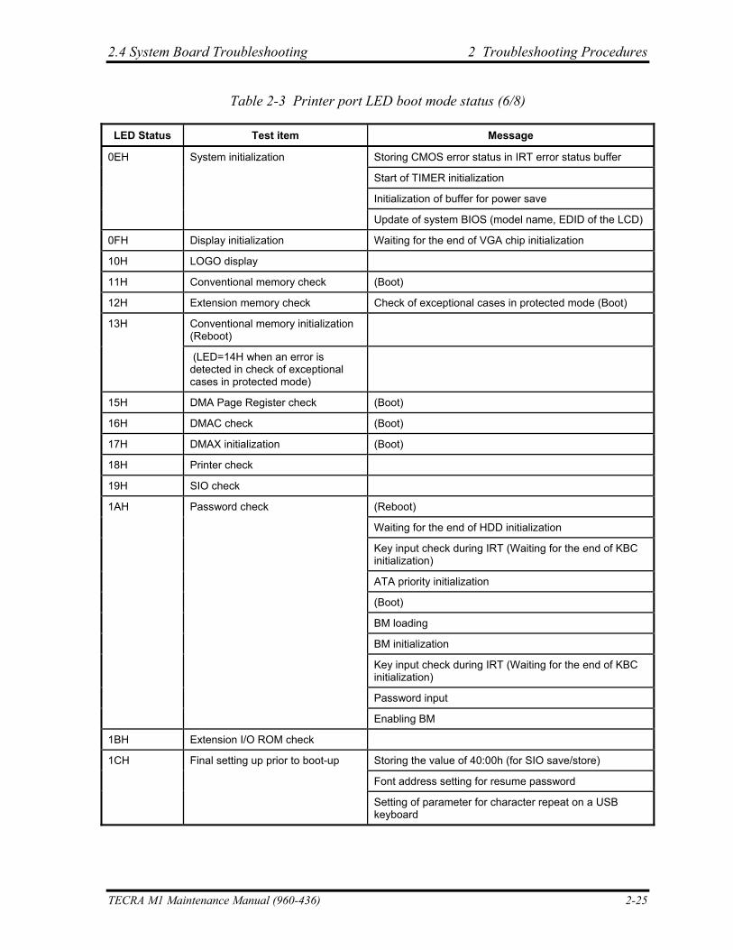
2.4 System Board Troubleshooting 2 Troubleshooting Procedures
Table 2-3 Printer port LED boot mode status (6/8)
LED Status Test item Message
Storing CMOS error status in IRT error status buffer
Start of TIMER initialization
Initialization of buffer for power save
0EH System initialization
Update of system BIOS (model name, EDID of the LCD)
0FH Display initialization Waiting for the end of VGA chip initialization
10H LOGO display
11H Conventional memory check (Boot)
12H Extension memory check Check of exceptional cases in protected mode (Boot)
Conventional memory initialization (Reboot)
13H
(LED=14H when an error is detected in check of exceptional cases in protected mode)
15H DMA Page Register check (Boot)
16H DMAC check (Boot)
17H DMAX initialization (Boot)
18H Printer check
19H SIO check
(Reboot)
Waiting for the end of HDD initialization
Key input check during IRT (Waiting for the end of KBC initialization)
ATA priority initialization
(Boot)
BM loading
BM initialization
Key input check during IRT (Waiting for the end of KBC initialization)
Password input
1AH Password check
Enabling BM
1BH Extension I/O ROM check
Storing the value of 40:00h (for SIO save/store)
Font address setting for resume password
1CH Final setting up prior to boot-up
Setting of parameter for character repeat on a USB keyboard
TECRA M1 Maintenance Manual (960-436) 2-25
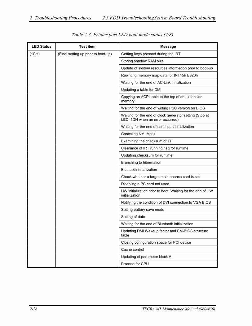
2 Troubleshooting Procedures 2.5 FDD TroubleshootingSystem Board Troubleshooting
Table 2-3 Printer port LED boot mode status (7/8)
LED Status Test item Message
Getting keys pressed during the IRT
Storing shadow RAM size
Update of system resources information prior to boot-up
Rewriting memory map data for INT15h E820h
Waiting for the end of AC-Link initialization
Updating a table for DMI
Copying an ACPI table to the top of an expansion memory
Waiting for the end of writing PSC version on BIOS
Waiting for the end of clock generator setting (Stop at LED=1DH when an error occurred)
Waiting for the end of serial port initialization
Canceling NMI Mask
Examining the checksum of TIT
Clearance of IRT running flag for runtime
Updating checksum for runtime
Branching to hibernation
Bluetooth initialization
Check whether a target maintenance card is set
Disabling a PC card not used
HW initialization prior to boot, Waiting for the end of HW initialization
Notifying the condition of DVI connection to VGA BIOS
Setting battery save mode
Setting of date
Waiting for the end of Bluetooth initialization
Updating DMI Wakeup factor and SM-BIOS structure table
Closing configuration space for PCI device
Cache control
Updating of parameter block A
(1CH) (Final setting up prior to boot-up)
Process for CPU
2-26 TECRA M1 Maintenance Manual (960-436)
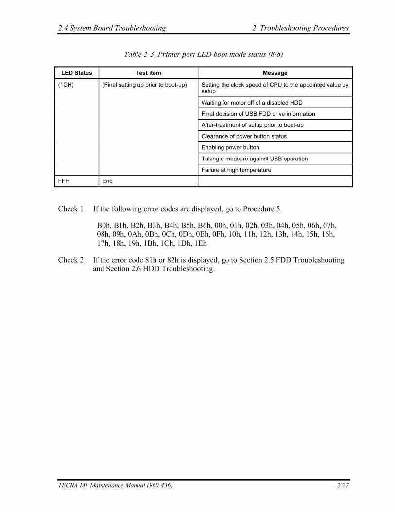
2.4 System Board Troubleshooting 2 Troubleshooting Procedures
Table 2-3 Printer port LED boot mode status (8/8)
LED Status Test item Message
Setting the clock speed of CPU to the appointed value by setup
Waiting for motor off of a disabled HDD
Final decision of USB FDD drive information
After-treatment of setup prior to boot-up
Clearance of power button status
Enabling power button
Taking a measure against USB operation
(1CH) (Final setting up prior to boot-up)
Failure at high temperature
FFH End
Check 1 If the following error codes are displayed, go to Procedure 5.
B0h, B1h, B2h, B3h, B4h, B5h, B6h, 00h, 01h, 02h, 03h, 04h, 05h, 06h, 07h, 08h, 09h, 0Ah, 0Bh, 0Ch, 0Dh, 0Eh, 0Fh, 10h, 11h, 12h, 13h, 14h, 15h, 16h, 17h, 18h, 19h, 1Bh, 1Ch, 1Dh, 1Eh
Check 2 If the error code 81h or 82h is displayed, go to Section 2.5 FDD Troubleshooting and Section 2.6 HDD Troubleshooting.
TECRA M1 Maintenance Manual (960-436) 2-27
2 Troubleshooting Procedures 2.5 FDD TroubleshootingSystem Board Troubleshooting
Procedure 3 Diagnostic Test Program Execution Check
Execute the following tests from the Diagnostic Test Menu. Refer to Chapter 3, Tests and Diagnostics, for more information on how to perform these tests.
1. System test
2. Memory test
3. Keyboard test
4. Display test
5. Floppy Disk test
6. Hard Disk test
7. Real Timer test
8. NDP test
9. Expansion test
10. Sound/Modem test
11. CD-ROM/DVD-ROM test
12. Bluetooth test
13. Wireless LAN test
If an error is detected during these tests, go to Procedure 3.
2-28 TECRA M1 Maintenance Manual (960-436)
2.4 System Board Troubleshooting 2 Troubleshooting Procedures
Procedure 4 Replacement Check
The system board connectors may be disconnected. Disassemble the computer following the steps described in Chapter 4, Replacement Procedures and perform Check 1.
Check 1 Visually check for the following:
a) Cracked or broken connector housing
b) Damaged connector pins
If their connectors are in good condition, but there is still a problem, go to Check 2.
Check 2 The system board may be damaged. Replace the system board with a new one following the steps described in Chapter 4, Replacement Procedures.
TECRA M1 Maintenance Manual (960-436) 2-29
2 Troubleshooting Procedures 2.5 FDD TroubleshootingFDD Troubleshooting
2.5 FDD Troubleshooting
This section describes how to determine if the FDD is functioning properly. Perform the steps below starting with Procedure 1 and continuing with the other procedures as required.
Procedure 1: FDD Head Cleaning Check
Procedure 2: Diagnostic Test Program Execution Check
Procedure 3: Connector Check and Replacement Check
Procedure 1 FDD Head Cleaning Check
FDD head cleaning operation details are given in Chapter 3, Tests and Diagnostics.
Insert the Diagnostics Disk in the computer’s floppy disk drive, turn on the computer and run the test. Clean the FDD heads using the cleaning kit. If the FDD still does not function properly after cleaning, go to Procedure 2.
If the test program cannot be executed, go to Procedure 3.
2-30 TECRA M1 Maintenance Manual (960-436)
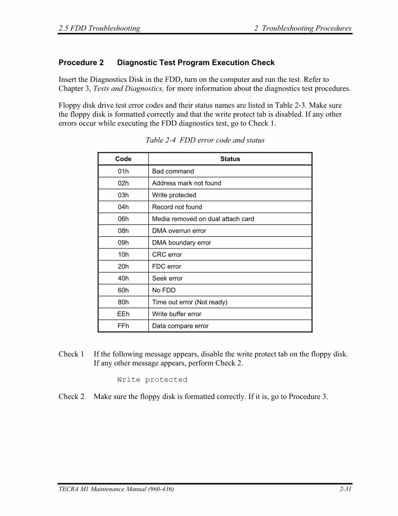
2.5 FDD Troubleshooting 2 Troubleshooting Procedures
Procedure 2 Diagnostic Test Program Execution Check
Insert the Diagnostics Disk in the FDD, turn on the computer and run the test. Refer to Chapter 3, Tests and Diagnostics, for more information about the diagnostics test procedures.
Floppy disk drive test error codes and their status names are listed in Table 2-3. Make sure the floppy disk is formatted correctly and that the write protect tab is disabled. If any other errors occur while executing the FDD diagnostics test, go to Check 1.
Table 2-4 FDD error code and status
Code Status
01h Bad command
02h Address mark not found
03h Write protected
04h Record not found
06h Media removed on dual attach card
08h DMA overrun error
09h DMA boundary error
10h CRC error
20h FDC error
40h Seek error
60h No FDD
80h Time out error (Not ready)
EEh Write buffer error
FFh Data compare error
Check 1 If the following message appears, disable the write protect tab on the floppy disk. If any other message appears, perform Check 2.
Write protected
Check 2 Make sure the floppy disk is formatted correctly. If it is, go to Procedure 3.
TECRA M1 Maintenance Manual (960-436) 2-31
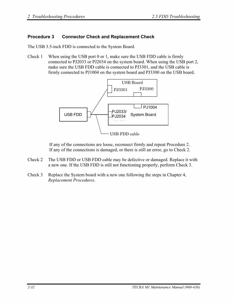
2 Troubleshooting Procedures 2.5 FDD Troubleshooting
Procedure 3 Connector Check and Replacement Check
The USB 3.5-inch FDD is connected to the System Board.
Check 1 When using the USB port 0 or 1, make sure the USB FDD cable is firmly connected to PJ2033 or PJ2034 on the system board. When using the USB port 2, make sure the USB FDD cable is connected to PJ3301, and the USB cable is firmly connected to PJ1004 on the system board and PJ3300 on the USB board.
PJ2033/PJ2034
PJ1004
USB BoardPJ3300PJ3301
USB FDD cable
If any of the connections are loose, reconnect firmly and repeat Procedure 2. If any of the connections is damaged, or there is still an error, go to Check 2.
Check 2 The USB FDD or USB FDD cable may be defective or damaged. Replace it with a new one. If the USB FDD is still not functioning properly, perform Check 3.
Check 3 Replace the System board with a new one following the steps in Chapter 4, Replacement Procedures.
2-32 TECRA M1 Maintenance Manual (960-436)
2.6 HDD Troubleshooting 2 Troubleshooting Procedures
2
2.6 HDD Troubleshooting
This section describes how to determine if the HDD is functioning properly. Perform the steps below starting with Procedure 1 and continuing with the other procedures as required.
Procedure 1: Message Check
Procedure 2: Partition Check
Procedure 3: Format Check
Procedure 4: Diagnostic Test Program Execution Check
Procedure 5: Connector Check and Replacement Check
CAUTION: The contents of the hard disk will be erased when you execute the HDD troubleshooting procedures. Transfer the contents of the hard disk to floppy disks or other storage media.
Procedure 1 Message Check
When the computer’s HDD does not function properly, some of the following error messages may appear on the display. Start with Check 1 below and perform the other checks as instructed.
Check 1 If any of the following messages appear, go to Procedure 5. If the following messages do not appear, perform Check 2.
HDC ERROR (After 5 seconds this message will disappear.) or
IDE #0 ERROR (After 5 seconds this message will disappear.) or
IDE #1 ERROR (After 5 seconds this message will disappear.)
Check 2 If either of the following messages appears, go to Procedure 2. If the following messages do not appear, perform Check 3.
Insert system disk in drive Press any key when ready ..... or Non-System disk or disk error Replace and press any key
Check 3 Make sure the Hard Disk option is set to not used. If it is set to not used, choose another setting and restart the computer. If the problem still exists, go to Procedure 2.
TECRA M1 Maintenance Manual (960-436) 2-33
2 Troubleshooting Procedures 2.6 HDD Troubleshooting
Procedure 2 Partition Check
Insert the Toshiba MS-DOS system disk and restart the computer with U key holding down. Perform the following checks:
Check 1 Type C: and press Enter. If you cannot change to drive C, go to Check 2. If you can change to drive C, go to Check 3.
Check 2 Type FDISK and press Enter. Choose Display Partition Information from the FDISK menu. If drive C is listed, go to Check 3. If drive C is not listed, return to the FDISK menu and choose the option to create a DOS partition on drive C. Restart the computer from the Toshiba MS-DOS system disk. If the problem still exists, go to Procedure 3.
Check 3 If drive C is listed as active in the FDISK menu, go to Check 4. If drive C is not listed as active, return to the FDISK menu and choose the option to set the active partition for drive C. Restart the computer and then go to Procedure 3.
Check 4 Remove the FD and restart the computer. If the problem still exists, go to Procedure 3.
Check 5 Using the SYS command on the Toshiba MS-DOS system disk, install system files on the HDD.
If the following message appears on the display, the system files have been transferred to the HDD. Restart the computer. If the problem still exists, go to Procedure 3.
System transferred
NOTE: If the computer is running Windows 2000, OSR2 or higher and the hard disk has more than 512 MB capacity, the FDISK program will ask if you need support for a partition larger than 2GB. Select Y for large partition support; however, be sure to read the precaution regarding access by other operating systems.
2-34 TECRA M1 Maintenance Manual (960-436)
2.6 HDD Troubleshooting 2 Troubleshooting Procedures
Procedure 3 Format Check
The computer’s HDD is formatted using the low level format program and the MS-DOS FORMAT program. To format the HDD, start with Check 1 below and perform the other steps as required.
Check 1 Format the HDD and transfer system files using FORMAT C:/S/U. If the following message appears on the display, the HDD is formatted.
Format complete
If an error message appears on the display, refer to the Toshiba MS-DOS Manual for more information and perform Check 2.
Check 2 Using the Diagnostics Disk, format the HDD with a low level format option. Refer to Chapter 3, Tests and Diagnostics for more information about the diagnostic program.
If the following message appears on the display, the HDD low level format is complete. Partition and format the HDD using the MS-DOS FORMAT command.
Format complete
If you cannot format the HDD using the Tests and Diagnostic program, go to Procedure 4.
TECRA M1 Maintenance Manual (960-436) 2-35
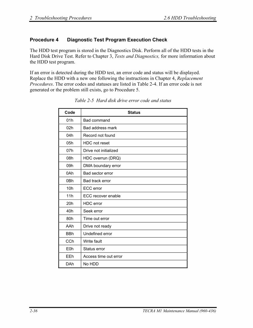
2 Troubleshooting Procedures 2.6 HDD Troubleshooting
Procedure 4 Diagnostic Test Program Execution Check
The HDD test program is stored in the Diagnostics Disk. Perform all of the HDD tests in the Hard Disk Drive Test. Refer to Chapter 3, Tests and Diagnostics, for more information about the HDD test program.
If an error is detected during the HDD test, an error code and status will be displayed. Replace the HDD with a new one following the instructions in Chapter 4, Replacement Procedures. The error codes and statuses are listed in Table 2-4. If an error code is not generated or the problem still exists, go to Procedure 5.
Table 2-5 Hard disk drive error code and status
Code Status
01h Bad command
02h Bad address mark
04h Record not found
05h HDC not reset
07h Drive not initialized
08h HDC overrun (DRQ)
09h DMA boundary error
0Ah Bad sector error
0Bh Bad track error
10h ECC error
11h ECC recover enable
20h HDC error
40h Seek error
80h Time out error
AAh Drive not ready
BBh Undefined error
CCh Write fault
E0h Status error
EEh Access time out error
DAh No HDD
2-36 TECRA M1 Maintenance Manual (960-436)
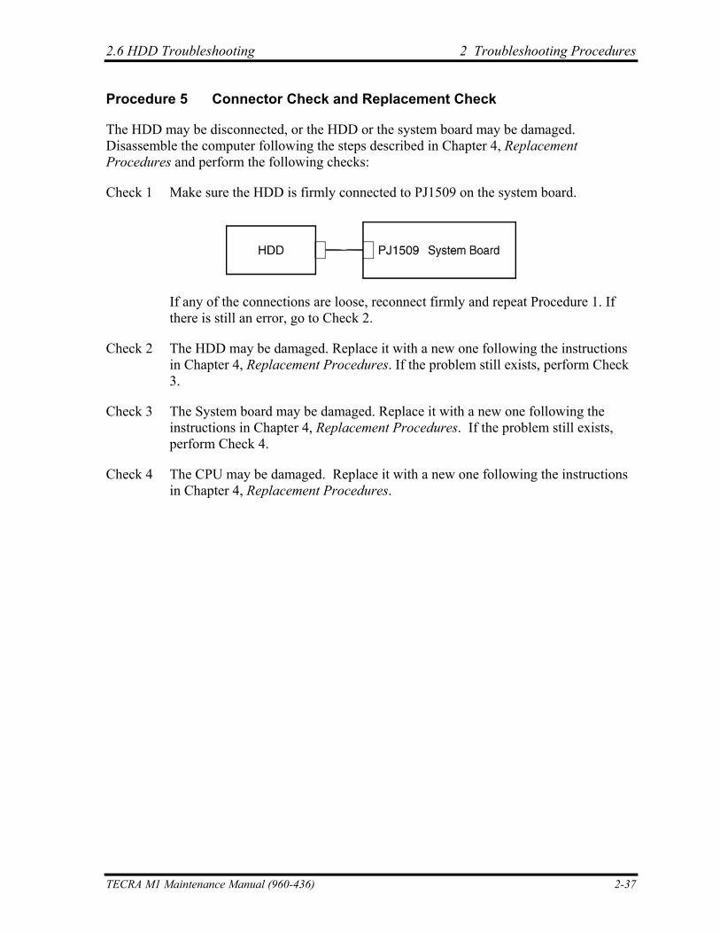
2.6 HDD Troubleshooting 2 Troubleshooting Procedures
Procedure 5 Connector Check and Replacement Check
The HDD may be disconnected, or the HDD or the system board may be damaged. Disassemble the computer following the steps described in Chapter 4, Replacement Procedures and perform the following checks:
Check 1 Make sure the HDD is firmly connected to PJ1509 on the system board.
If any of the connections are loose, reconnect firmly and repeat Procedure 1. If there is still an error, go to Check 2.
Check 2 The HDD may be damaged. Replace it with a new one following the instructions in Chapter 4, Replacement Procedures. If the problem still exists, perform Check 3.
Check 3 The System board may be damaged. Replace it with a new one following the instructions in Chapter 4, Replacement Procedures. If the problem still exists, perform Check 4.
Check 4 The CPU may be damaged. Replace it with a new one following the instructions in Chapter 4, Replacement Procedures.
TECRA M1 Maintenance Manual (960-436) 2-37
2 Troubleshooting Procedures 2.7 Keyboard and Touch pad Troubleshooting
2.7 Keyboard and Touch pad Troubleshooting
To determine if the computer’s keyboard or touch pad is functioning properly, perform the following procedures. Start with Procedure 1 and continue with the other procedures as instructed.
Procedure 1: Diagnostic Test Program Execution Check
Procedure 2: Connector and Replacement Check
Procedure 1 Diagnostic Test Program Execution Check
Execute the Keyboard Test in the Diagnostic Program. Refer to Chapter 3, Tests and Diagnostics, for more information on how to perform the test program.
If an error occurs, go to Procedure 2. If an error does not occur, the keyboard is functioning properly.
2-38 TECRA M1 Maintenance Manual (960-436)
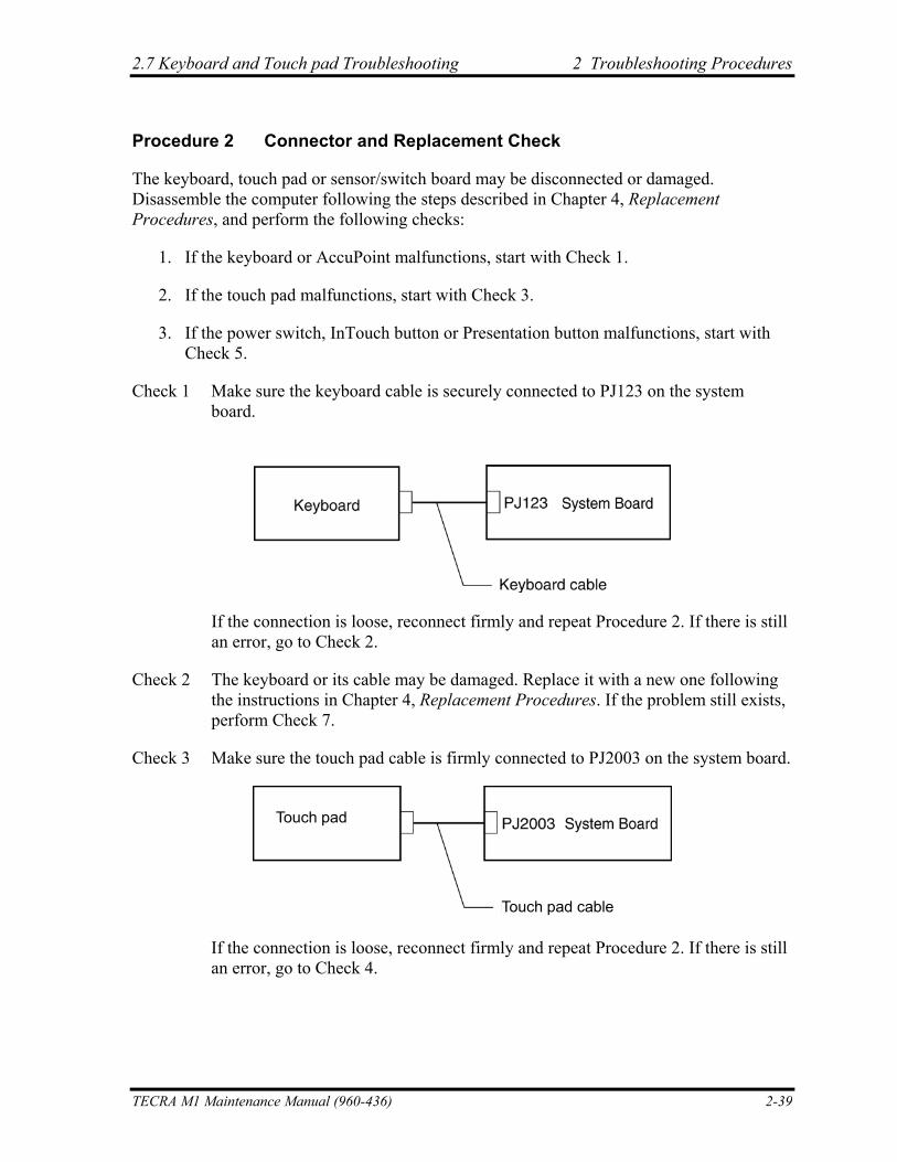
2.7 Keyboard and Touch pad Troubleshooting 2 Troubleshooting Procedures
Procedure 2 Connector and Replacement Check
The keyboard, touch pad or sensor/switch board may be disconnected or damaged. Disassemble the computer following the steps described in Chapter 4, Replacement Procedures, and perform the following checks:
1. If the keyboard or AccuPoint malfunctions, start with Check 1.
2. If the touch pad malfunctions, start with Check 3.
3. If the power switch, InTouch button or Presentation button malfunctions, start with Check 5.
Check 1 Make sure the keyboard cable is securely connected to PJ123 on the system board.
If the connection is loose, reconnect firmly and repeat Procedure 2. If there is still an error, go to Check 2.
Check 2 The keyboard or its cable may be damaged. Replace it with a new one following the instructions in Chapter 4, Replacement Procedures. If the problem still exists, perform Check 7.
Check 3 Make sure the touch pad cable is firmly connected to PJ2003 on the system board.
Touch pad
Touch pad cable
If the connection is loose, reconnect firmly and repeat Procedure 2. If there is still an error, go to Check 4.
TECRA M1 Maintenance Manual (960-436) 2-39
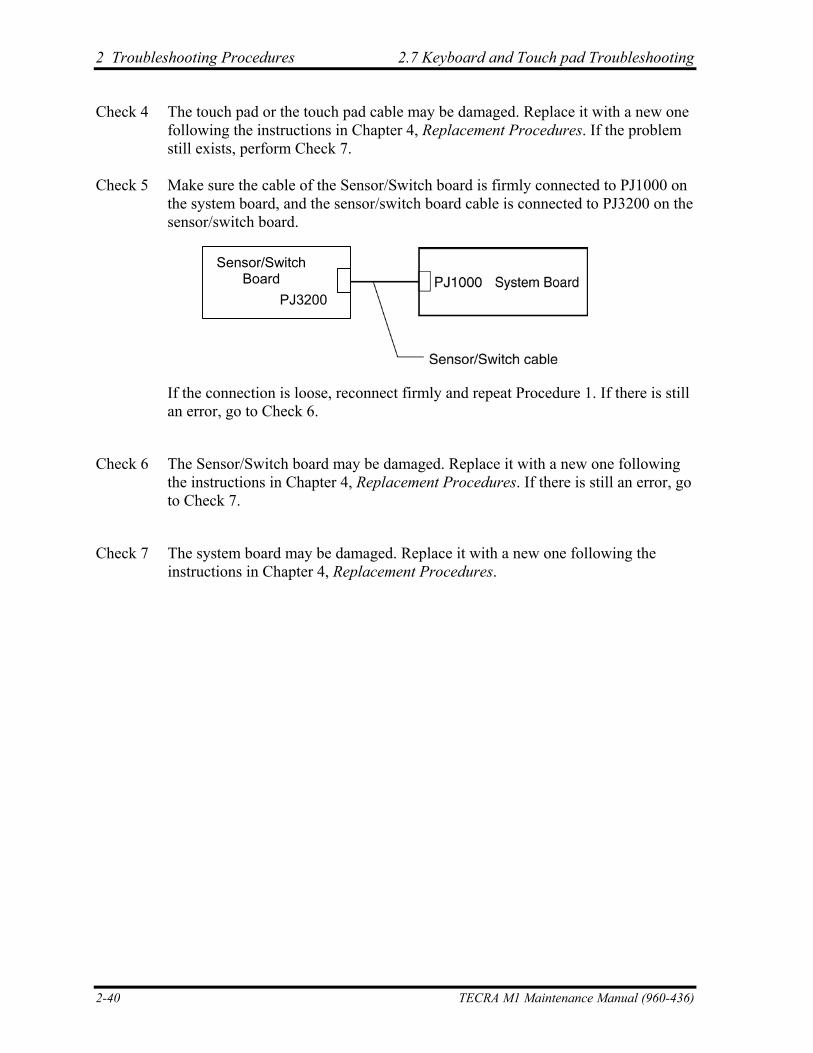
2 Troubleshooting Procedures 2.7 Keyboard and Touch pad Troubleshooting
Check 4 The touch pad or the touch pad cable may be damaged. Replace it with a new one following the instructions in Chapter 4, Replacement Procedures. If the problem still exists, perform Check 7.
Check 5 Make sure the cable of the Sensor/Switch board is firmly connected to PJ1000 on
the system board, and the sensor/switch board cable is connected to PJ3200 on the sensor/switch board.
Sensor/SwitchBoard
PJ3200
If the connection is loose, reconnect firmly and repeat Procedure 1. If there is still an error, go to Check 6.
Check 6 The Sensor/Switch board may be damaged. Replace it with a new one following the instructions in Chapter 4, Replacement Procedures. If there is still an error, go to Check 7.
Check 7 The system board may be damaged. Replace it with a new one following the instructions in Chapter 4, Replacement Procedures.
2-40 TECRA M1 Maintenance Manual (960-436)
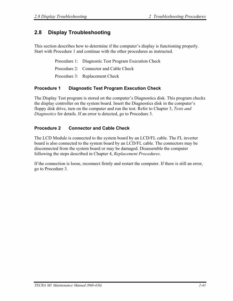
2.8 Display Troubleshooting 2 Troubleshooting Procedures
2.8 Display Troubleshooting
This section describes how to determine if the computer’s display is functioning properly. Start with Procedure 1 and continue with the other procedures as instructed.
Procedure 1: Diagnostic Test Program Execution Check
Procedure 2: Connector and Cable Check
Procedure 3: Replacement Check
Procedure 1 Diagnostic Test Program Execution Check
The Display Test program is stored on the computer’s Diagnostics disk. This program checks the display controller on the system board. Insert the Diagnostics disk in the computer’s floppy disk drive, turn on the computer and run the test. Refer to Chapter 3, Tests and Diagnostics for details. If an error is detected, go to Procedure 3.
Procedure 2 Connector and Cable Check
The LCD Module is connected to the system board by an LCD/FL cable. The FL inverter board is also connected to the system board by an LCD/FL cable. The connectors may be disconnected from the system board or may be damaged. Disassemble the computer following the steps described in Chapter 4, Replacement Procedures.
If the connection is loose, reconnect firmly and restart the computer. If there is still an error, go to Procedure 3.
TECRA M1 Maintenance Manual (960-436) 2-41
2 Troubleshooting Procedures 2.8 Display Troubleshooting
Procedure 3 Replacement Check
The FL, FL inverter board, LCD module, and system board are connected to display circuits. Any of these components may be damaged. Refer to Chapter 4, Replacement Procedures, for instructions on how to disassemble the computer and then perform the following checks:
If the FL does not light, perform Check 1.
If characters or graphics are not displayed clearly, perform Check 1.
If some screen functions do not operate properly, perform Check 3.
If the FL remains lit when the display is closed, perform Check 5.
Check 1 Replace the FL with a new one following the instructions in Chapter 4, Replacement Procedures and test the display again. If the problem still exists, perform Check2.
Check 2 Replace the FL with a new one following the instructions in Chapter 4, Replacement Procedures and test the display again. If the problem still exists, perform Check 3.
Check 3 Replace the LCD module with a new one following the instructions in Chapter 4, Replacement Procedures and test the display again. If the problem still exists, perform Check 4.
Check 4 Replace the display cable (FL cable and LCD cable) with a new one following the instructions in Chapter 4, Replacement Procedures and test the display again. If the problem still exists, perform Check 5.
Check 5 The display controller on the system board may be damaged. Replace it with a new one following the instructions in Chapter 4, Replacement Procedures.
2-42 TECRA M1 Maintenance Manual (960-436)
2.9 CD-ROM Drive Troubleshooting 2 Troubleshooting Procedures
2.9 CD-ROM Drive Troubleshooting
This section describes how to determine if the computer’s internal CD-ROM drive is functioning properly. Perform the steps below starting with Procedure 1 and continue with the other procedures as required.
Procedure 1: Diagnostic Test Program Execution Check
Procedure 2: Connector Check and Replacement Check
Procedure 1 Diagnostic Test Program Execution Check
The CD-ROM/DVD-ROM test program is stored in the Diagnostics Disk.
For the CD-ROM test, prepare a test CD-RW.
Then insert the Diagnostics Disk in the computer’s floppy disk drive, turn on the computer and run the test. Refer to Chapter 3, Tests and Diagnostics, for more information about the diagnostics test procedures.
If any errors occur while executing the CD-ROM/DVD-ROM test, go to Procedure 2.
TECRA M1 Maintenance Manual (960-436) 2-43
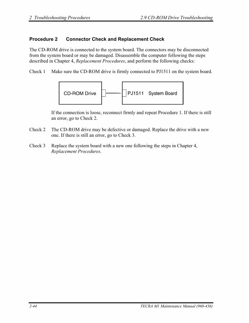
2 Troubleshooting Procedures 2.9 CD-ROM Drive Troubleshooting
Procedure 2 Connector Check and Replacement Check
The CD-ROM drive is connected to the system board. The connectors may be disconnected from the system board or may be damaged. Disassemble the computer following the steps described in Chapter 4, Replacement Procedures, and perform the following checks:
Check 1 Make sure the CD-ROM drive is firmly connected to PJ1511 on the system board.
If the connection is loose, reconnect firmly and repeat Procedure 1. If there is still an error, go to Check 2.
Check 2 The CD-ROM drive may be defective or damaged. Replace the drive with a new one. If there is still an error, go to Check 3.
Check 3 Replace the system board with a new one following the steps in Chapter 4, Replacement Procedures.
2-44 TECRA M1 Maintenance Manual (960-436)
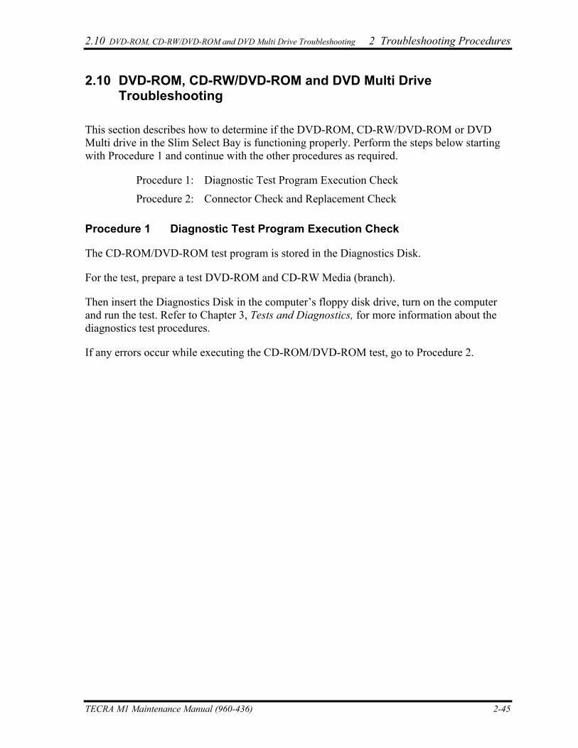
2.10 DVD-ROM, CD-RW/DVD-ROM and DVD Multi Drive Troubleshooting 2 Troubleshooting Procedures
2.10 DVD-ROM, CD-RW/DVD-ROM and DVD Multi Drive Troubleshooting
This section describes how to determine if the DVD-ROM, CD-RW/DVD-ROM or DVD Multi drive in the Slim Select Bay is functioning properly. Perform the steps below starting with Procedure 1 and continue with the other procedures as required.
Procedure 1: Diagnostic Test Program Execution Check
Procedure 2: Connector Check and Replacement Check
Procedure 1 Diagnostic Test Program Execution Check
The CD-ROM/DVD-ROM test program is stored in the Diagnostics Disk.
For the test, prepare a test DVD-ROM and CD-RW Media (branch).
Then insert the Diagnostics Disk in the computer’s floppy disk drive, turn on the computer and run the test. Refer to Chapter 3, Tests and Diagnostics, for more information about the diagnostics test procedures.
If any errors occur while executing the CD-ROM/DVD-ROM test, go to Procedure 2.
TECRA M1 Maintenance Manual (960-436) 2-45
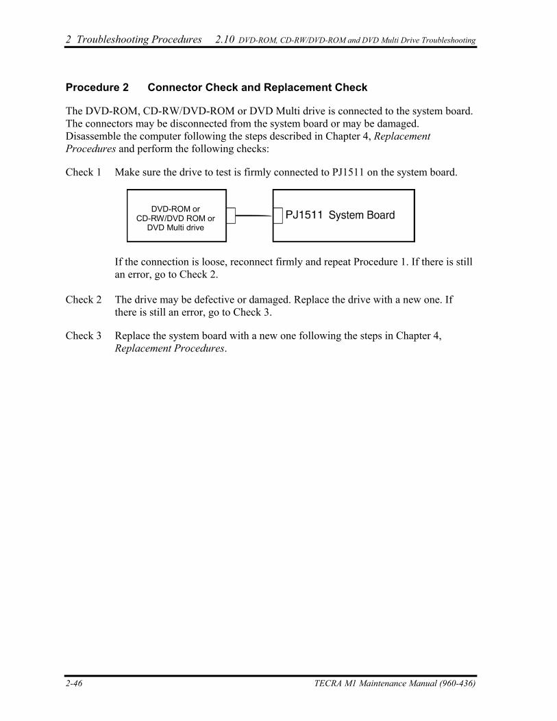
2 Troubleshooting Procedures 2.10 DVD-ROM, CD-RW/DVD-ROM and DVD Multi Drive Troubleshooting
Procedure 2 Connector Check and Replacement Check
The DVD-ROM, CD-RW/DVD-ROM or DVD Multi drive is connected to the system board. The connectors may be disconnected from the system board or may be damaged. Disassemble the computer following the steps described in Chapter 4, Replacement Procedures and perform the following checks:
Check 1 Make sure the drive to test is firmly connected to PJ1511 on the system board.
DVD-ROM orCD-RW/DVD ROM or
DVD Multi drive
If the connection is loose, reconnect firmly and repeat Procedure 1. If there is still an error, go to Check 2.
Check 2 The drive may be defective or damaged. Replace the drive with a new one. If there is still an error, go to Check 3.
Check 3 Replace the system board with a new one following the steps in Chapter 4, Replacement Procedures.
2-46 TECRA M1 Maintenance Manual (960-436)
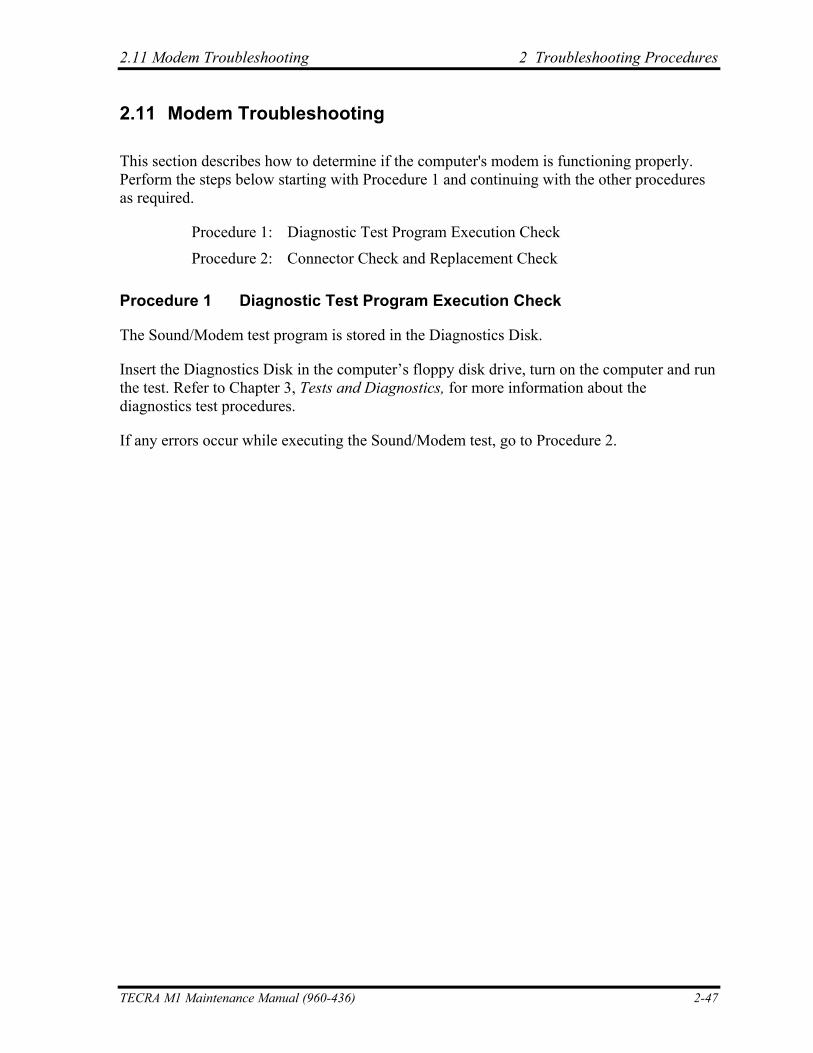
2.11 Modem Troubleshooting 2 Troubleshooting Procedures
2.11 Modem Troubleshooting
This section describes how to determine if the computer's modem is functioning properly. Perform the steps below starting with Procedure 1 and continuing with the other procedures as required.
Procedure 1: Diagnostic Test Program Execution Check
Procedure 2: Connector Check and Replacement Check
Procedure 1 Diagnostic Test Program Execution Check
The Sound/Modem test program is stored in the Diagnostics Disk.
Insert the Diagnostics Disk in the computer’s floppy disk drive, turn on the computer and run the test. Refer to Chapter 3, Tests and Diagnostics, for more information about the diagnostics test procedures.
If any errors occur while executing the Sound/Modem test, go to Procedure 2.
TECRA M1 Maintenance Manual (960-436) 2-47
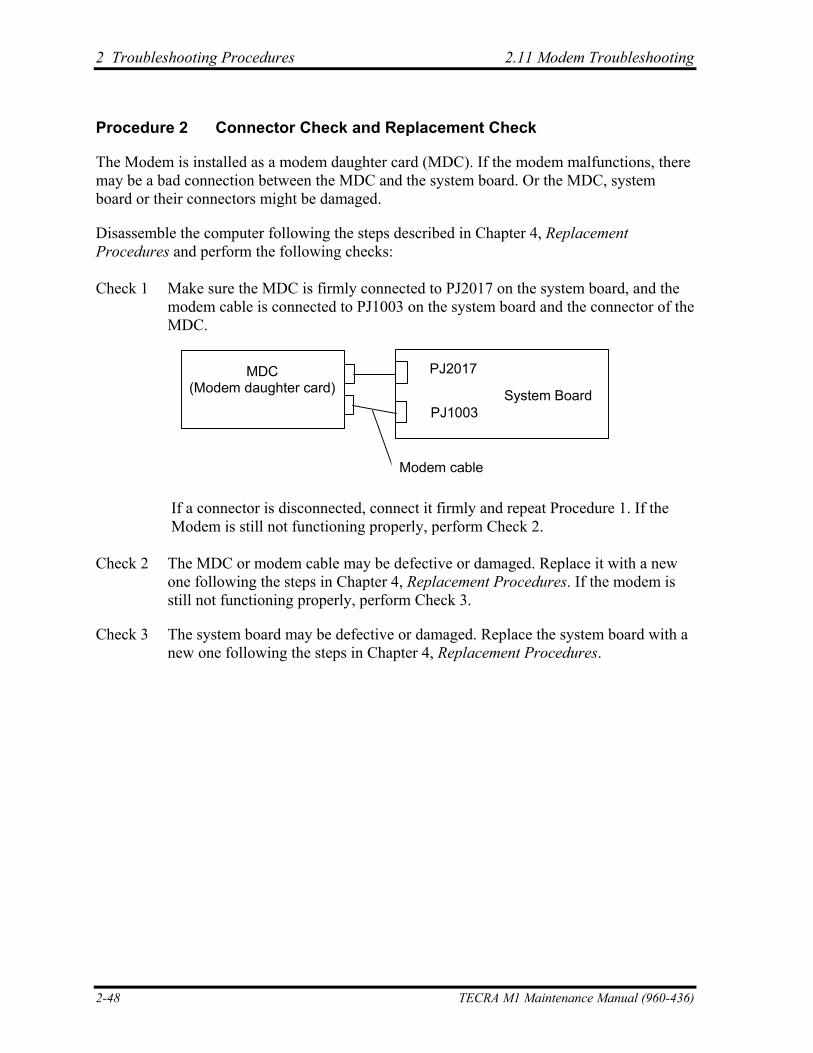
2 Troubleshooting Procedures 2.11 Modem Troubleshooting
Procedure 2 Connector Check and Replacement Check
The Modem is installed as a modem daughter card (MDC). If the modem malfunctions, there may be a bad connection between the MDC and the system board. Or the MDC, system board or their connectors might be damaged.
Disassemble the computer following the steps described in Chapter 4, Replacement Procedures and perform the following checks:
Check 1 Make sure the MDC is firmly connected to PJ2017 on the system board, and the modem cable is connected to PJ1003 on the system board and the connector of the MDC.
MDC(Modem daughter card) System Board
PJ2017
PJ1003
Modem cable
If a connector is disconnected, connect it firmly and repeat Procedure 1. If the Modem is still not functioning properly, perform Check 2.
Check 2 The MDC or modem cable may be defective or damaged. Replace it with a new one following the steps in Chapter 4, Replacement Procedures. If the modem is still not functioning properly, perform Check 3.
Check 3 The system board may be defective or damaged. Replace the system board with a new one following the steps in Chapter 4, Replacement Procedures.
2-48 TECRA M1 Maintenance Manual (960-436)
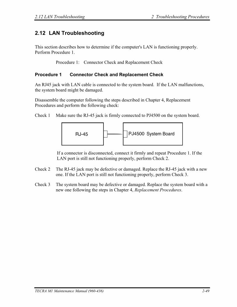
2.12 LAN Troubleshooting 2 Troubleshooting Procedures
2.12 LAN Troubleshooting
This section describes how to determine if the computer's LAN is functioning properly. Perform Procedure 1.
Procedure 1: Connector Check and Replacement Check
Procedure 1 Connector Check and Replacement Check
An RJ45 jack with LAN cable is connected to the system board. If the LAN malfunctions, the system board might be damaged.
Disassemble the computer following the steps described in Chapter 4, Replacement Procedures and perform the following check:
Check 1 Make sure the RJ-45 jack is firmly connected to PJ4500 on the system board.
If a connector is disconnected, connect it firmly and repeat Procedure 1. If the LAN port is still not functioning properly, perform Check 2.
Check 2 The RJ-45 jack may be defective or damaged. Replace the RJ-45 jack with a new one. If the LAN port is still not functioning properly, perform Check 3.
Check 3 The system board may be defective or damaged. Replace the system board with a new one following the steps in Chapter 4, Replacement Procedures.
TECRA M1 Maintenance Manual (960-436) 2-49
2 Troubleshooting Procedures 2.13 Bluetooth Troubleshooting
2.13 Bluetooth Troubleshooting
This section describes how to determine if the computer's Bluetooth is functioning properly. Perform the steps below starting with Procedure 1 and continuing with the other procedures as required.
Procedure 1: Transmitting-Receiving Check
Procedure 2: Antennas' Connection Check
Procedure 3: Antenna Check
Procedure 4: Replacement Check
Procedure 1 Transmitting-Receiving Check
Make sure the wireless switch on the left side of the computer is turned ON. If it is not, slide the switch toward the back of the computer to turn it on.
Check 1 Execute test program ICH_BT73.EXE to check the BD_ADDR of the Bluetooth. Perform the test following the instructions described in Chapter 3, Bluetooth Test Program (ICH_BT73.EXE).
If the computer passes the test, the function is correctly working. If the computer does not pass the test, the Bluetooth board may be disconnected or damaged. Make sure the connector on the Bluetooth board is firmly connected to PJ4900 on the system board. And perform the test program ICH_BT73.EXE again.
If the computer still does not pass the test, go to check 3.
Check 2 Execute test program ICH_BT53.EXE to check the transmitting-receiving function of the Bluetooth. You will need a second computer that can communicate by the Bluetooth. Perform the test following the instructions described in Chapter 3, Bluetooth Test Program (ICH_BT53.EXE).
If the computer passes the test, the function is correctly working. If the computer does not pass the test, go to check 3.
Check 3 The Bluetooth board may be defective or damaged. Replace it with a new one. And perform the test program again.
If the computer still does not pass the test, go to Procedure 2.
2-50 TECRA M1 Maintenance Manual (960-436)
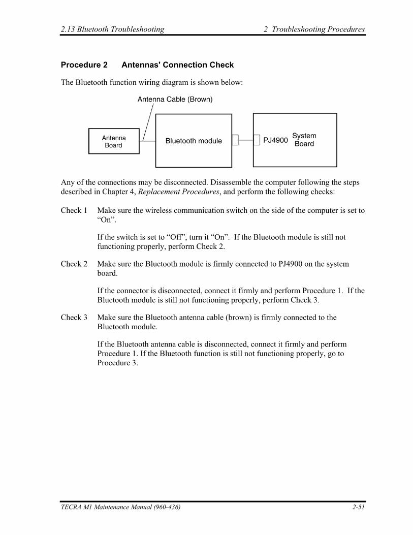
2.13 Bluetooth Troubleshooting 2 Troubleshooting Procedures
Procedure 2 Antennas' Connection Check
The Bluetooth function wiring diagram is shown below:
Any of the connections may be disconnected. Disassemble the computer following the steps described in Chapter 4, Replacement Procedures, and perform the following checks:
Check 1 Make sure the wireless communication switch on the side of the computer is set to “On”.
If the switch is set to “Off”, turn it “On”. If the Bluetooth module is still not functioning properly, perform Check 2.
Check 2 Make sure the Bluetooth module is firmly connected to PJ4900 on the system board.
If the connector is disconnected, connect it firmly and perform Procedure 1. If the Bluetooth module is still not functioning properly, perform Check 3.
Check 3 Make sure the Bluetooth antenna cable (brown) is firmly connected to the Bluetooth module.
If the Bluetooth antenna cable is disconnected, connect it firmly and perform Procedure 1. If the Bluetooth function is still not functioning properly, go to Procedure 3.
TECRA M1 Maintenance Manual (960-436) 2-51
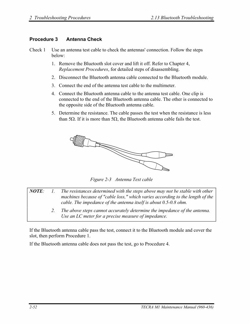
2 Troubleshooting Procedures 2.13 Bluetooth Troubleshooting
Procedure 3 Antenna Check
Check 1 Use an antenna test cable to check the antennas' connection. Follow the steps below:
1. Remove the Bluetooth slot cover and lift it off. Refer to Chapter 4, Replacement Procedures, for detailed steps of disassembling.
2. Disconnect the Bluetooth antenna cable connected to the Bluetooth module.
3. Connect the end of the antenna test cable to the multimeter.
4. Connect the Bluetooth antenna cable to the antenna test cable. One clip is connected to the end of the Bluetooth antenna cable. The other is connected to the opposite side of the Bluetooth antenna cable.
5. Determine the resistance. The cable passes the test when the resistance is less than 5Ω. If it is more than 5Ω, the Bluetooth antenna cable fails the test.
Figure 2-3 Antenna Test cable
NOTE: 1. The resistances determined with the steps above may not be stable with other machines because of "cable loss," which varies according to the length of the cable. The impedance of the antenna itself is about 0.5-0.8 ohm.
2. The above steps cannot accurately determine the impedance of the antenna. Use an LC meter for a precise measure of impedance.
If the Bluetooth antenna cable pass the test, connect it to the Bluetooth module and cover the slot, then perform Procedure 1.
If the Bluetooth antenna cable does not pass the test, go to Procedure 4.
2-52 TECRA M1 Maintenance Manual (960-436)
2.13 Bluetooth Troubleshooting 2 Troubleshooting Procedures
Procedure 4 Replacement Check
Check 1 The Bluetooth module may be defective or damaged. Replace the Bluetooth module with a new one following the steps in Chapter 4, Replacement Procedures. If the Bluetooth is still not functioning properly, perform Check 2.
Check 2 The system board may be defective or damaged. Replace the system board with a new one following the steps in Chapter 4, Replacement Procedures.
TECRA M1 Maintenance Manual (960-436) 2-53
2 Troubleshooting Procedures 2.14 Wireless LAN Troubleshooting
2.14 Wireless LAN Troubleshooting
This section describes how to determine if the computer's Wireless LAN is functioning properly. Perform the steps below starting with Procedure 1 and continuing with the other procedures as required.
Procedure 1: Transmitting-Receiving Check
Procedure 2: Antennas' Connection Check
Procedure 3: Antennas' Capability Check
Procedure 4: Replacement Check
Procedure 1 Transmitting-Receiving Check
Make sure the wireless switch on the left side of the computer is turned ON. If it is not, slide the switch toward the back of the computer to turn it on.
Check 1 Execute the test program to check the transmitting-receiving function of the wireless LAN. You will need a second computer that can communicate by the wireless LAN. Perform the test following the instructions described in Section 3.16-18, Wireless LAN Test Program.
If the computer passes the test, the function is correctly working.
If the computer does not pass the test, perform Procedure 2.
2-54 TECRA M1 Maintenance Manual (960-436)
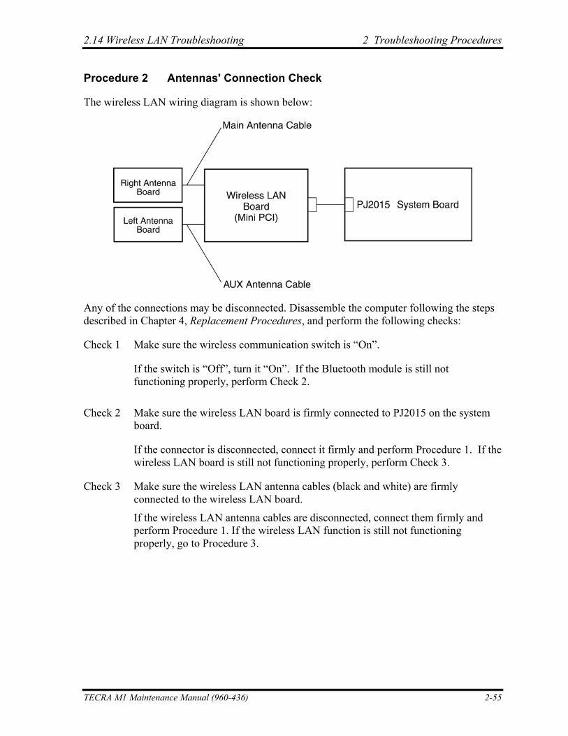
2.14 Wireless LAN Troubleshooting 2 Troubleshooting Procedures
Procedure 2 Antennas' Connection Check
The wireless LAN wiring diagram is shown below:
Any of the connections may be disconnected. Disassemble the computer following the steps described in Chapter 4, Replacement Procedures, and perform the following checks:
Check 1 Make sure the wireless communication switch is “On”.
If the switch is “Off”, turn it “On”. If the Bluetooth module is still not functioning properly, perform Check 2.
Check 2 Make sure the wireless LAN board is firmly connected to PJ2015 on the system
board.
If the connector is disconnected, connect it firmly and perform Procedure 1. If the wireless LAN board is still not functioning properly, perform Check 3.
Check 3 Make sure the wireless LAN antenna cables (black and white) are firmly connected to the wireless LAN board.
If the wireless LAN antenna cables are disconnected, connect them firmly and perform Procedure 1. If the wireless LAN function is still not functioning properly, go to Procedure 3.
TECRA M1 Maintenance Manual (960-436) 2-55
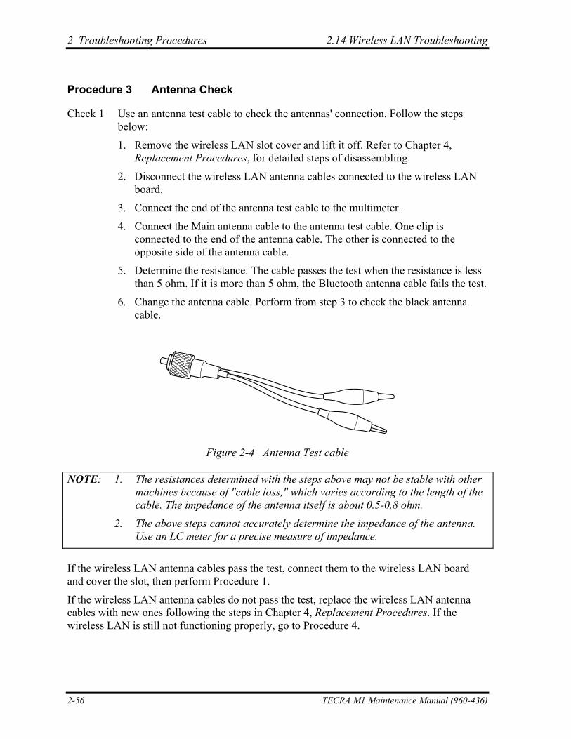
2 Troubleshooting Procedures 2.14 Wireless LAN Troubleshooting
Procedure 3 Antenna Check
Check 1 Use an antenna test cable to check the antennas' connection. Follow the steps below:
1. Remove the wireless LAN slot cover and lift it off. Refer to Chapter 4, Replacement Procedures, for detailed steps of disassembling.
2. Disconnect the wireless LAN antenna cables connected to the wireless LAN board.
3. Connect the end of the antenna test cable to the multimeter.
4. Connect the Main antenna cable to the antenna test cable. One clip is connected to the end of the antenna cable. The other is connected to the opposite side of the antenna cable.
5. Determine the resistance. The cable passes the test when the resistance is less than 5 ohm. If it is more than 5 ohm, the Bluetooth antenna cable fails the test.
6. Change the antenna cable. Perform from step 3 to check the black antenna cable.
Figure 2-4 Antenna Test cable
NOTE: 1. The resistances determined with the steps above may not be stable with other machines because of "cable loss," which varies according to the length of the cable. The impedance of the antenna itself is about 0.5-0.8 ohm.
2. The above steps cannot accurately determine the impedance of the antenna. Use an LC meter for a precise measure of impedance.
If the wireless LAN antenna cables pass the test, connect them to the wireless LAN board and cover the slot, then perform Procedure 1.
If the wireless LAN antenna cables do not pass the test, replace the wireless LAN antenna cables with new ones following the steps in Chapter 4, Replacement Procedures. If the wireless LAN is still not functioning properly, go to Procedure 4.
2-56 TECRA M1 Maintenance Manual (960-436)
2.14 Wireless LAN Troubleshooting 2 Troubleshooting Procedures
Procedure 4 Replacement Check
The wireless LAN board, and the system board are connected to the circuits. Any of these components may be damaged. Refer to Chapter 4, Replacement Procedures, for instructions on how to disassemble the computer and then perform the following checks:
Check 1 The wireless LAN board may be defective or damaged. Replace the board with a
new one following the steps in Chapter 4, Replacement Procedures. If the problem still exists, perform Check2.
Check 2 The system board may be defective or damaged. Replace the board with a new one following the instructions in Chapter 4, Replacement Procedures and test the display again.
TECRA M1 Maintenance Manual (960-436) 2-57
2 Troubleshooting Procedures 2.15 Sound Troubleshooting
2.15 Sound Troubleshooting
This section describes how to determine if the computer's sound functions are functioning properly. Perform the steps below starting with Procedure 1 and continuing with the other procedures as required.
Procedure 1: Diagnostic Test Program Execution Check
Procedure 2: Connector Check
Procedure 3: Replacement Check
Procedure 1 Diagnostic Test Program Execution Check
The Sound/Modem test program is stored on the computer’s diagnostic disk. Insert the Diagnostics disk in the computer's floppy disk drive, turn on the computer and run the test. Refer to Chapter 3, Tests and Diagnostics, for details.
If an error is detected, go to Procedure 2.
2-58 TECRA M1 Maintenance Manual (960-436)
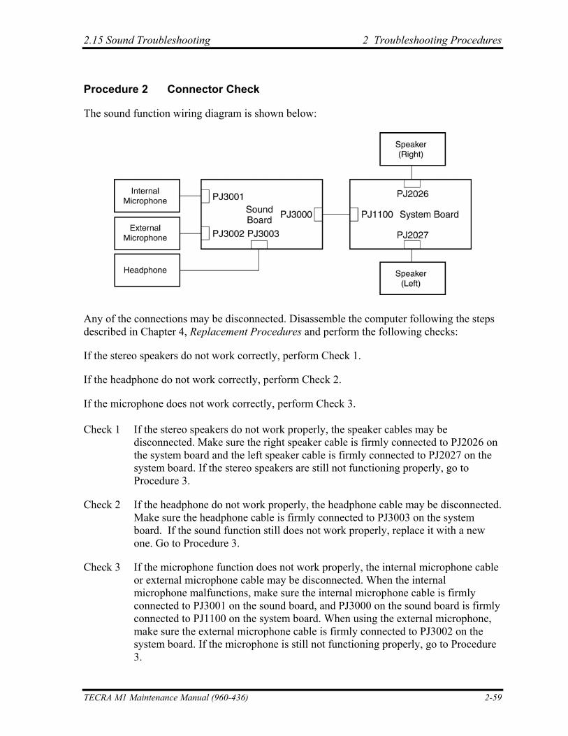
2.15 Sound Troubleshooting 2 Troubleshooting Procedures
Procedure 2 Connector Check
The sound function wiring diagram is shown below:
Any of the connections may be disconnected. Disassemble the computer following the steps described in Chapter 4, Replacement Procedures and perform the following checks:
If the stereo speakers do not work correctly, perform Check 1.
If the headphone do not work correctly, perform Check 2.
If the microphone does not work correctly, perform Check 3.
Check 1 If the stereo speakers do not work properly, the speaker cables may be disconnected. Make sure the right speaker cable is firmly connected to PJ2026 on the system board and the left speaker cable is firmly connected to PJ2027 on the system board. If the stereo speakers are still not functioning properly, go to Procedure 3.
Check 2 If the headphone do not work properly, the headphone cable may be disconnected. Make sure the headphone cable is firmly connected to PJ3003 on the system board. If the sound function still does not work properly, replace it with a new one. Go to Procedure 3.
Check 3 If the microphone function does not work properly, the internal microphone cable or external microphone cable may be disconnected. When the internal microphone malfunctions, make sure the internal microphone cable is firmly connected to PJ3001 on the sound board, and PJ3000 on the sound board is firmly connected to PJ1100 on the system board. When using the external microphone, make sure the external microphone cable is firmly connected to PJ3002 on the system board. If the microphone is still not functioning properly, go to Procedure 3.
TECRA M1 Maintenance Manual (960-436) 2-59
2 Troubleshooting Procedures 2.15 Sound Troubleshooting
Procedure 3 Replacement Check
Check 1 If the stereo speakers do not sound properly, the right or left speaker may be defective or damaged. Replace it with a new one. If the stereo speakers still do not work properly, go to Check 5.
Check 2 If the headphone don't sound properly, the headphone jack may be defective or damaged. Replace it with a new one. If the sound function still does not work properly, go to Check 5.
Check 3 If the microphone does not work properly, the microphone cable may be defective or damaged. Replace it with a new one. If the microphone still does not work properly, go to Check 4.
Check 4 The sound board or system board may be defective or damaged. Replace it with a new one.
2-60 TECRA M1 Maintenance Manual (960-436)
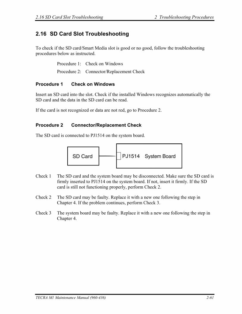
2.16 SD Card Slot Troubleshooting 2 Troubleshooting Procedures
2.16 SD Card Slot Troubleshooting
To check if the SD card/Smart Media slot is good or no good, follow the troubleshooting procedures below as instructed.
Procedure 1: Check on Windows
Procedure 2: Connector/Replacement Check
Procedure 1 Check on Windows
Insert an SD card into the slot. Check if the installed Windows recognizes automatically the SD card and the data in the SD card can be read.
If the card is not recognized or data are not red, go to Procedure 2.
Procedure 2 Connector/Replacement Check
The SD card is connected to PJ1514 on the system board.
Check 1 The SD card and the system board may be disconnected. Make sure the SD card is firmly inserted to PJ1514 on the system board. If not, insert it firmly. If the SD card is still not functioning properly, perform Check 2.
Check 2 The SD card may be faulty. Replace it with a new one following the step in Chapter 4. If the problem continues, perform Check 3.
Check 3 The system board may be faulty. Replace it with a new one following the step in Chapter 4.
TECRA M1 Maintenance Manual (960-436) 2-61
2 Troubleshooting Procedures 2.16 SD Card Slot Troubleshooting
2-62 TECRA M1 Maintenance Manual (960-436)
Chapter 3 Tests and Diagnostics

3 Tests and Diagnostics
3-ii TECRA M1 Maintenance Manual (960-436)
3 Tests and Diagnostics
Chapter 3 Contents
3.1 The Diagnostic Test ................................................................................................... 3-1
3.2 Executing the Diagnostic Test ................................................................................... 3-3
3.3 Subtest Names............................................................................................................ 3-7
3.4 System Test.............................................................................................................. 3-10
3.5 Memory Test............................................................................................................ 3-13
3.6 Keyboard Test.......................................................................................................... 3-15
3.7 Display Test ............................................................................................................. 3-19
3.8 Floppy Disk Test...................................................................................................... 3-23
3.9 Printer Test............................................................................................................... 3-25
3.10 Async Test ............................................................................................................... 3-27
3.11 Hard Disk Test ......................................................................................................... 3-29
3.12 Real Timer Test........................................................................................................ 3-32
3.13 NDP Test.................................................................................................................. 3-34
3.14 Expansion Test......................................................................................................... 3-35
3.15 CD-ROM/DVD-ROM Test ..................................................................................... 3-36
3.16 Wireless LAN Test (Agere) ..................................................................................... 3-37
3.17 Wireless LAN Test (Atheros) .................................................................................. 3-42
3.18 Wireless LAN Test (Caelxico) ................................................................................ 3-45
3.19 Sound/Modem Test.................................................................................................. 3-46
3.20 IEEE1394 Test ......................................................................................................... 3-50
3.21 Bluetooth Test.......................................................................................................... 3-52
3.22 Error Code and Error Status Names ........................................................................ 3-61
3.23 Hard Disk Test Detail Status ................................................................................... 3-64
3.24 Head Cleaning.......................................................................................................... 3-66
3.24.1 Function Description .......................................................................... 3-66
3.24.2 Operations .......................................................................................... 3-66
3.25 Log Utilities ............................................................................................................. 3-67
3.25.1 Function Description .......................................................................... 3-67
3.25.2 Operations .......................................................................................... 3-67
3.26 Running Test............................................................................................................ 3-69
TECRA M1 Maintenance Manual (960-436) 3-iii
3 Tests and Diagnostics
3-iv TECRA M1 Maintenance Manual (960-436)
3.26.1 Function Description .......................................................................... 3-69
3.26.2 Operations .......................................................................................... 3-69
3.27 Floppy Disk Drive Utilities...................................................................................... 3-71
3.27.1 Function Description .......................................................................... 3-71
3.27.2 Operations .......................................................................................... 3-72
3.28 System Configuration .............................................................................................. 3-76
3.28.1 Function Description .......................................................................... 3-76
3.28.2 Operations .......................................................................................... 3-77
3.29 SETUP ..................................................................................................................... 3-78
3.29.1 Function Description .......................................................................... 3-78
3.29.2 Accessing the SETUP Program.......................................................... 3-80
Tables
Table 3-1 Subtest names................................................................................................. 3-7
Table 3-2 Error code for Bluetooth test (BD_ADDR)................................................. 3-55
Table 3-3 Error code for Bluetooth test (BD_ADDR of the DUT).............................. 3-59
Table 3-4 Error codes and error status names .............................................................. 3-61
Table 3-5 Hard disk controller status register contents................................................ 3-64
Table 3-6 Error register contents.................................................................................. 3-65
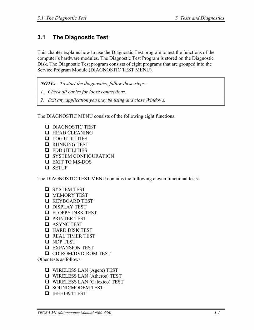
3.1 The Diagnostic Test 3 Tests and Diagnostics
3
3.1 The Diagnostic Test
This chapter explains how to use the Diagnostic Test program to test the functions of the computer’s hardware modules. The Diagnostic Test Program is stored on the Diagnostic Disk. The Diagnostic Test program consists of eight programs that are grouped into the Service Program Module (DIAGNOSTIC TEST MENU).
NOTE: To start the diagnostics, follow these steps:
1. Check all cables for loose connections.
2. Exit any application you may be using and close Windows.
The DIAGNOSTIC MENU consists of the following eight functions.
DIAGNOSTIC TEST HEAD CLEANING LOG UTILITIES RUNNING TEST FDD UTILITIES SYSTEM CONFIGURATION EXIT TO MS-DOS SETUP
The DIAGNOSTIC TEST MENU contains the following eleven functional tests:
SYSTEM TEST MEMORY TEST KEYBOARD TEST DISPLAY TEST FLOPPY DISK TEST PRINTER TEST ASYNC TEST HARD DISK TEST REAL TIMER TEST NDP TEST EXPANSION TEST CD-ROM/DVD-ROM TEST
Other tests as follows
WIRELESS LAN (Agere) TEST WIRELESS LAN (Atheros) TEST WIRELESS LAN (Calexico) TEST SOUND/MODEM TEST IEEE1394 TEST
TECRA M1 Maintenance Manual (960-436) 3-1
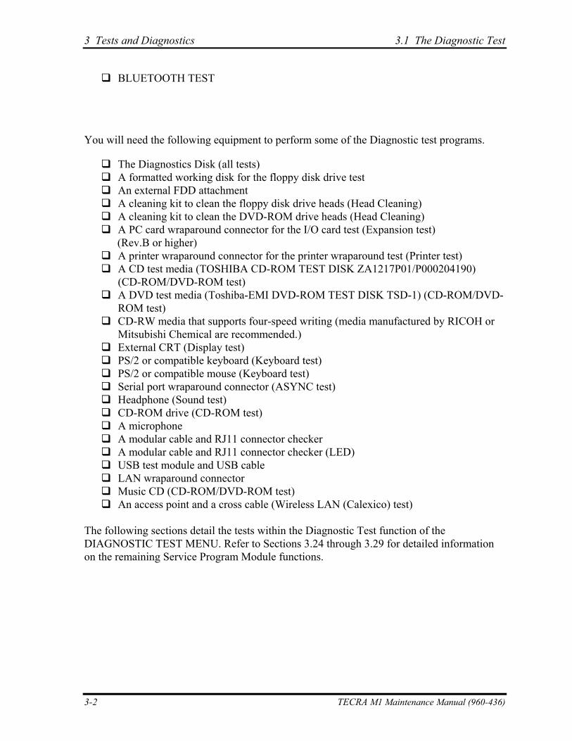
3 Tests and Diagnostics 3.1 The Diagnostic Test
BLUETOOTH TEST
You will need the following equipment to perform some of the Diagnostic test programs.
The Diagnostics Disk (all tests) A formatted working disk for the floppy disk drive test An external FDD attachment A cleaning kit to clean the floppy disk drive heads (Head Cleaning) A cleaning kit to clean the DVD-ROM drive heads (Head Cleaning) A PC card wraparound connector for the I/O card test (Expansion test)
(Rev.B or higher) A printer wraparound connector for the printer wraparound test (Printer test) A CD test media (TOSHIBA CD-ROM TEST DISK ZA1217P01/P000204190)
(CD-ROM/DVD-ROM test) A DVD test media (Toshiba-EMI DVD-ROM TEST DISK TSD-1) (CD-ROM/DVD-
ROM test) CD-RW media that supports four-speed writing (media manufactured by RICOH or
Mitsubishi Chemical are recommended.) External CRT (Display test) PS/2 or compatible keyboard (Keyboard test) PS/2 or compatible mouse (Keyboard test) Serial port wraparound connector (ASYNC test) Headphone (Sound test) CD-ROM drive (CD-ROM test) A microphone A modular cable and RJ11 connector checker A modular cable and RJ11 connector checker (LED) USB test module and USB cable LAN wraparound connector Music CD (CD-ROM/DVD-ROM test) An access point and a cross cable (Wireless LAN (Calexico) test)
The following sections detail the tests within the Diagnostic Test function of the DIAGNOSTIC TEST MENU. Refer to Sections 3.24 through 3.29 for detailed information on the remaining Service Program Module functions.
3-2 TECRA M1 Maintenance Manual (960-436)
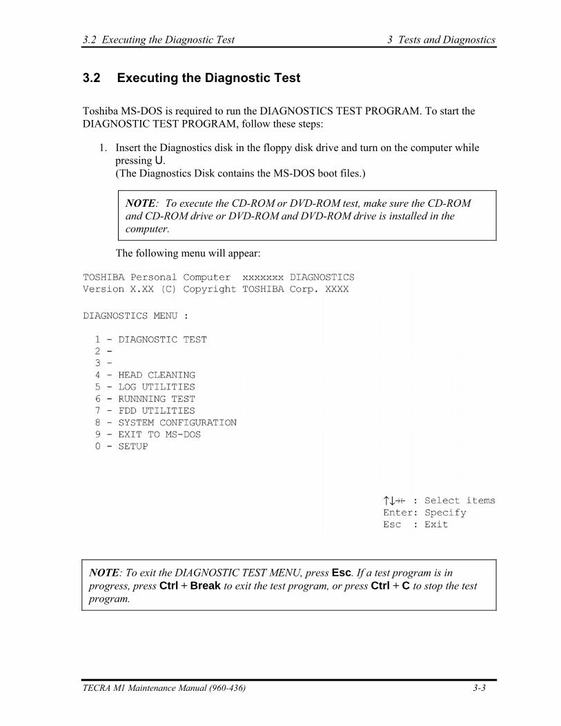
3.2 Executing the Diagnostic Test 3 Tests and Diagnostics
3.2 Executing the Diagnostic Test
Toshiba MS-DOS is required to run the DIAGNOSTICS TEST PROGRAM. To start the DIAGNOSTIC TEST PROGRAM, follow these steps:
1. Insert the Diagnostics disk in the floppy disk drive and turn on the computer while pressing U. (The Diagnostics Disk contains the MS-DOS boot files.)
NOTE: To execute the CD-ROM or DVD-ROM test, make sure the CD-ROM and CD-ROM drive or DVD-ROM and DVD-ROM drive is installed in the computer.
The following menu will appear:
NOTE: To exit the DIAGNOSTIC TEST MENU, press Esc. If a test program is in progress, press Ctrl + Break to exit the test program, or press Ctrl + C to stop the test program.
TECRA M1 Maintenance Manual (960-436) 3-3
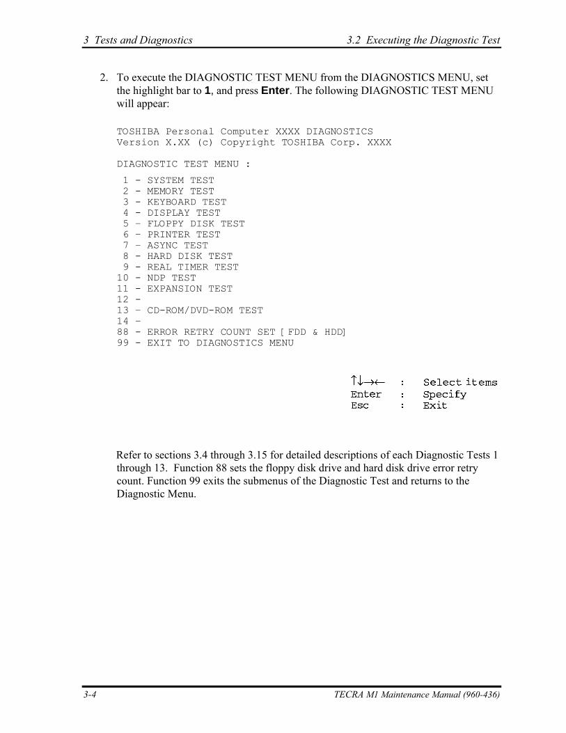
3 Tests and Diagnostics 3.2 Executing the Diagnostic Test
2. To execute the DIAGNOSTIC TEST MENU from the DIAGNOSTICS MENU, set the highlight bar to 1, and press Enter. The following DIAGNOSTIC TEST MENU will appear:
TOSHIBA Personal Computer XXXX DIAGNOSTICS Version X.XX (c) Copyright TOSHIBA Corp. XXXX DIAGNOSTIC TEST MENU :
1 - SYSTEM TEST 2 - MEMORY TEST 3 - KEYBOARD TEST 4 - DISPLAY TEST 5 – FLOPPY DISK TEST 6 – PRINTER TEST 7 – ASYNC TEST 8 - HARD DISK TEST 9 - REAL TIMER TEST 10 - NDP TEST 11 - EXPANSION TEST 12 - 13 – CD-ROM/DVD-ROM TEST 14 – 88 - ERROR RETRY COUNT SET [FDD & HDD] 99 - EXIT TO DIAGNOSTICS MENU
Refer to sections 3.4 through 3.15 for detailed descriptions of each Diagnostic Tests 1 through 13. Function 88 sets the floppy disk drive and hard disk drive error retry count. Function 99 exits the submenus of the Diagnostic Test and returns to the Diagnostic Menu.
3-4 TECRA M1 Maintenance Manual (960-436)
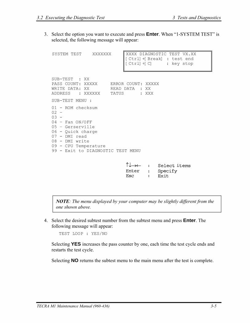
3.2 Executing the Diagnostic Test 3 Tests and Diagnostics
3. Select the option you want to execute and press Enter. When “1-SYSTEM TEST” is selected, the following message will appear:
SYSTEM TEST XXXXXXX XXXX DIAGNOSTIC TEST VX.XX
[Ctrl]+[Break] : test end [Ctrl]+[C] : key stop
SUB-TEST : XX PASS COUNT: XXXXX ERROR COUNT: XXXXX WRITE DATA: XX READ DATA : XX ADDRESS : XXXXXX TATUS : XXX
SUB-TEST MENU :
01 - ROM checksum 02 – 03 - 04 – Fan ON/OFF 05 – Gerserville 06 - Quick charge 07 - DMI read 08 - DMI write 09 - CPU Temperature 99 - Exit to DIAGNOSTIC TEST MENU
NOTE: The menu displayed by your computer may be slightly different from the one shown above.
4. Select the desired subtest number from the subtest menu and press Enter. The following message will appear:
TEST LOOP : YES/NO
Selecting YES increases the pass counter by one, each time the test cycle ends and restarts the test cycle.
Selecting NO returns the subtest menu to the main menu after the test is complete.
TECRA M1 Maintenance Manual (960-436) 3-5
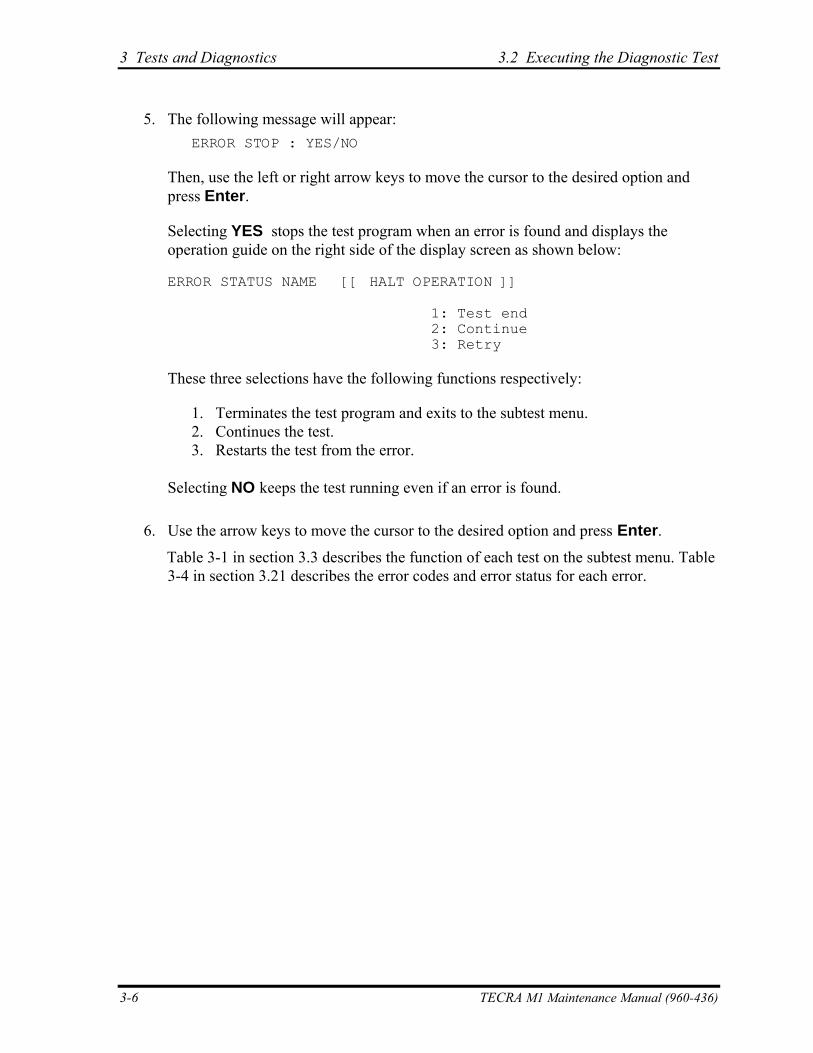
3 Tests and Diagnostics 3.2 Executing the Diagnostic Test
5. The following message will appear: ERROR STOP : YES/NO
Then, use the left or right arrow keys to move the cursor to the desired option and press Enter.
Selecting YES stops the test program when an error is found and displays the operation guide on the right side of the display screen as shown below:
ERROR STATUS NAME [[ HALT OPERATION ]]
1: Test end 2: Continue 3: Retry
These three selections have the following functions respectively:
1. Terminates the test program and exits to the subtest menu. 2. Continues the test. 3. Restarts the test from the error.
Selecting NO keeps the test running even if an error is found.
6. Use the arrow keys to move the cursor to the desired option and press Enter.
Table 3-1 in section 3.3 describes the function of each test on the subtest menu. Table 3-4 in section 3.21 describes the error codes and error status for each error.
3-6 TECRA M1 Maintenance Manual (960-436)
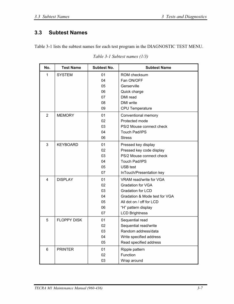
3.3 Subtest Names 3 Tests and Diagnostics
3.3 Subtest Names
Table 3-1 lists the subtest names for each test program in the DIAGNOSTIC TEST MENU.
Table 3-1 Subtest names (1/3)
No. Test Name Subtest No. Subtest Name
1 SYSTEM 01 04 05 06 07 08 09
ROM checksum Fan ON/OFF Gerserville Quick charge DMI read DMI write CPU Temperature
2 MEMORY 01 02 03 04 06
Conventional memory Protected mode PS/2 Mouse connect check Touch Pad/IPS Stress
3 KEYBOARD 01 02 03 04 05 07
Pressed key display Pressed key code display PS/2 Mouse connect check Touch Pad/IPS USB test InTouch/Presentation key
4 DISPLAY 01 02 03 04 05 06 07
VRAM read/write for VGA Gradation for VGA Gradation for LCD Gradation & Mode test for VGA All dot on / off for LCD “H” pattern display LCD Brightness
5 FLOPPY DISK 01 02 03 04 05
Sequential read Sequential read/write Random address/data Write specified address Read specified address
6 PRINTER 01 02 03
Ripple pattern Function Wrap around
TECRA M1 Maintenance Manual (960-436) 3-7
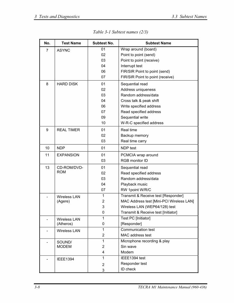
3 Tests and Diagnostics 3.3 Subtest Names
Table 3-1 Subtest names (2/3)
No. Test Name Subtest No. Subtest Name
7 ASYNC 01 02 03 04 06 07
Wrap around (board) Point to point (send) Point to point (receive) Interrupt test FIR/SIR Point to point (send) FIR/SIR Point to point (receive)
8 HARD DISK 01 02 03 04 06 07 09 10
Sequential read Address uniqueness Random address/data Cross talk & peak shift Write specified address Read specified address Sequential write W-R-C specified address
9 REAL TIMER 01 02 03
Real time Backup memory Real time carry
10 NDP 01 NDP test
11 EXPANSION 01 03
PCMCIA wrap around RGB monitor ID
13 CD-ROM/DVD-ROM
01 02 03 04 07
Sequential read Read specified address Random address/data Playback music RW 1point W/R/C
- Wireless LAN (Agere)
1 2 3 0
Transmit & Receive test [Responder] MAC Address test [Mini-PCI Wireless LAN] Wireless LAN (WEP64/128) test Transmit & Receive test [Initiator]
- Wireless LAN (Atheros)
1 0
Test PC [Initiator] [Responder]
- Wireless LAN 1 2
Communication test MAC address test
- SOUND/ MODEM
1 2 4
Microphone recording & play Sin wave Modem
- IEEE1394 1
2 3
IEEE1394 test Responder test ID check
3-8 TECRA M1 Maintenance Manual (960-436)
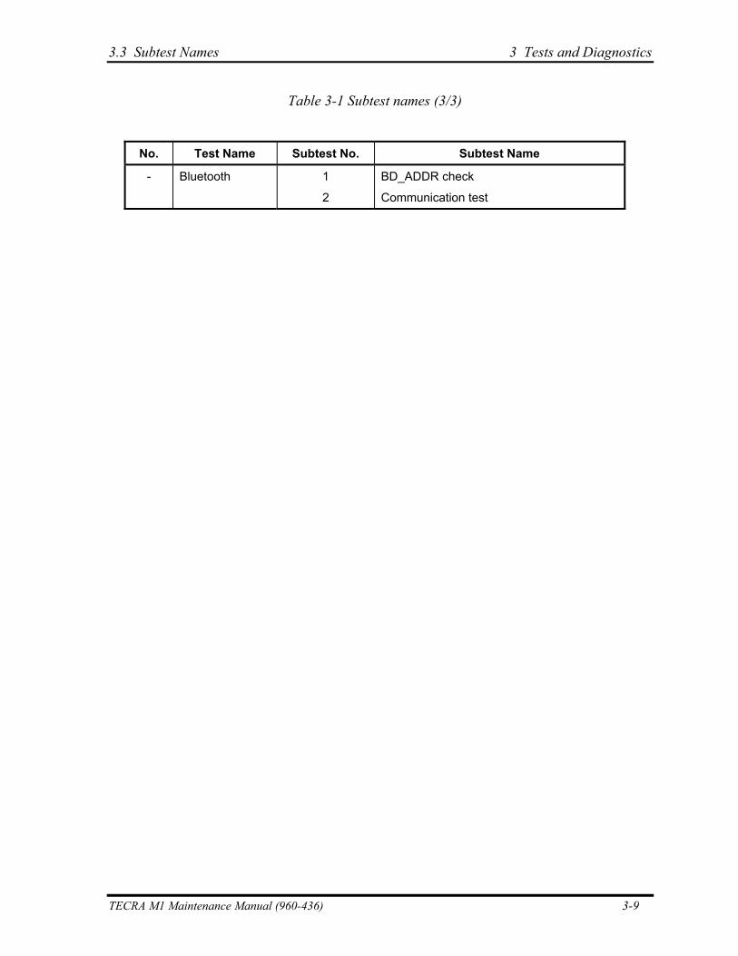
3.3 Subtest Names 3 Tests and Diagnostics
Table 3-1 Subtest names (3/3)
No. Test Name Subtest No. Subtest Name
-
Bluetooth 1
2
BD_ADDR check
Communication test
TECRA M1 Maintenance Manual (960-436) 3-9
3 Tests and Diagnostics 3.4 System Test
3.4 System Test
To execute the System Test select 1 from the DIAGNOSTIC TEST MENU, press Enter and follow the directions on the screen. Move the highlight bar to the subtest you want to execute and press Enter.
Subtest 01 ROM Checksum
This subtest executes a checksum test of the BIOS ROM on the System Board.
Subtest 04 Fan On/Off
This subtest checks CPU fan operation using the on/off command. The following message will appear when this subtest is executed. Make sure the fan does not rotate and press Enter.
*** Test Fan Revolution 0000RPM Start
The following message will appear. Make sure the fan rotates at low speed and press Enter.
*** Test Fan Revolution Low speed start
The following message will appear. Make sure the fan rotates at high speed and press Enter.
*** Test Fan Revolution High speed start
Subtest 05 Gerserville
If the CPU supports Gerserville (SpeedStep), this Subtest checks that the CPU operating clock speed can be changed.
Subtest 06 Quick charge
This subtest checks the status for the quick charge.
Subtest 07 DMI read
Reads the factory setting for the serial and DMI numbers.
Model Name : XXXXXX Version Number : XXXXXX-XXXXX Serial Number : XXXXXXXXXX Model Number : XXXXXX-XXXXX PCN/BND Number : XXXXXXXXXXXXXXXXXXXX UUID Number : XXXXXXXXXXXXXXXXXXXXXXXXX
3-10 TECRA M1 Maintenance Manual (960-436)
3.4 System Test 3 Tests and Diagnostics
To exit this subtest and return to the SYSTEM TEST menu, press Enter.
TECRA M1 Maintenance Manual (960-436) 3-11
3 Tests and Diagnostics 3.4 System Test
Subtest 08 DMI write
The following messages appear in order. When this subtest is executed. Input each information. (If you do not replace the PCB, the DMI information should not be changed.)
1. “Enter Model Name ?” is displayed.
Input the computer’s model name and press Enter. (e.g. TECRA M1)
2. “Enter Version Number ?”
Input the computer’s version number and press Enter. (e.g. PS245U-AAA13)
3. “Enter Serial Number ?”
Input the computer’s serial number and press Enter. (e.g. Z2020855JU)
4. “Enter Model Number ?”
Input the computer’s sales model number and press Enter. (e.g. PS245U-AAA13)
5. “Enter Bundle Number ?”
Input the computer’s PCN/Bundle number and press Enter. (e.g. PCN1190CCZ01/S3A1320D990)
6. “Write data OK (Y/N) ?”
When Y is press, the DMI information is written to the Flash-ROM.
3-12 TECRA M1 Maintenance Manual (960-436)
3.4 System Test 3 Tests and Diagnostics
Subtest 09 CPU Temperature
This subtest measures the CPU temperature to see if the cooling functions of the computer are effectively working.
When the subtest starts, the following message appears on the display:
CPU TEMP = XX deg C Throttling level = XXXXh
The number of the CPU TEMP indicates the CPU temperature at the moment in decimal notation. For example, if the number is 57, the CPU temperature is 57 degrees.
The number of “Throttling level” indicates how much the CPU has slowed. This number takes one of the following three values:
0000h : The CPU is running full speed. 4000h : The CPU has slowed to 75% of its maximum speed. 8000h : The CPU has slowed to 50% of its maximum speed.
The subtest displays the message five times at intervals of one minute; therefore, it takes five minutes to complete the test. The computer passes the test if the CPU temperature is less than 70 degrees at the end of the test. If the temperature is 70 degrees or more, the computer fails the test, and an error message appears on the display.
TECRA M1 Maintenance Manual (960-436) 3-13
3 Tests and Diagnostics 3.5 Memory Test
3.5 Memory Test
To execute the Memory Test, select 2 from the DIAGNOSTIC TEST MENU, press Enter and follow the directions on the screen. Move the highlight bar to the subtest you want to execute and press Enter.
Subtest 01 Conventional memory
This subtest writes constant data to conventional memory (0 to 640 KB), then reads the new data and compares the result with the original data.
Subtest 02 Protected Mode
NOTE: The CONFIG.SYS file must be configured without expanded memory manager programs such as EMM386.EXE, EMM386.SYS or QEMM386.SYS. Also, the HIMEM.SYS must be deleted from the CONFIG.SYS file.
This subtest writes constant data and address data to extended memory (maximum address 100000h) then reads the new data and compares the result with the original data.
The constant data is FFh, AAh, 55h, and 00h.
3-14 TECRA M1 Maintenance Manual (960-436)
3.5 Memory Test 3 Tests and Diagnostics
Subtest 04 Cache Memory
To test the cache memory, a pass-through write-read comparison of ‘5A’ data is run repeatedly to the test area (‘7000’:‘Program’ size to ‘7000’:‘7FFF’ (32 KB)) to check the hit-miss ratio (on/off status) for CPU cache memory. One test takes 3 seconds.
Number of misses < Number of hits → OK Number of misses ≥ Number of hits → Fail
Subtest 05 L2 Cache Memory
To test the L2 cache memory, a test similar to that for the cache memory is performed.
Subtest 06 Stress
The conventional memory is provided with a write/read buffer (size 1b30 h) and creates write data in the write buffer. Subsequent to 1 MB, the data is written in the write buffer and is read into the read buffer, followed by a data comparison up to the maximum memory size.
TECRA M1 Maintenance Manual (960-436) 3-15
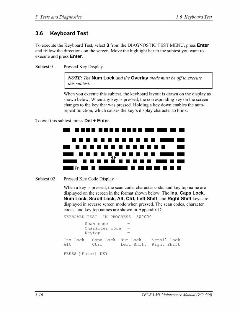
3 Tests and Diagnostics 3.6 Keyboard Test
3.6 Keyboard Test
To execute the Keyboard Test, select 3 from the DIAGNOSTIC TEST MENU, press Enter and follow the directions on the screen. Move the highlight bar to the subtest you want to execute and press Enter.
Subtest 01 Pressed Key Display
NOTE: The Num Lock and the Overlay mode must be off to execute this subtest.
When you execute this subtest, the keyboard layout is drawn on the display as shown below. When any key is pressed, the corresponding key on the screen changes to the key that was pressed. Holding a key down enables the auto-repeat function, which causes the key’s display character to blink.
To exit this subtest, press Del + Enter.
Fn
Subtest 02 Pressed Key Code Display
When a key is pressed, the scan code, character code, and key top name are displayed on the screen in the format shown below. The Ins, Caps Lock, Num Lock, Scroll Lock, Alt, Ctrl, Left Shift, and Right Shift keys are displayed in reverse screen mode when pressed. The scan codes, character codes, and key top names are shown in Appendix D. KEYBOARD TEST IN PROGRESS 302000
Scan code = Character code = Keytop =
Ins Lock Caps Lock Num Lock Scroll Lock Alt Ctrl Left Shift Right Shift PRESS [Enter] KEY
3-16 TECRA M1 Maintenance Manual (960-436)
3.6 Keyboard Test 3 Tests and Diagnostics
Subtest 03 PS/2 Mouse Connect Check
NOTE: To execute the PS/2 mouse connect check, a PS/2 mouse must be connected to the computer before the power is turned on.
This subtest checks whether a PS/2 mouse is connected or not. If this test does not detect an error, it returns to the subtest menu. If this test detects an error, the following message appears.
DATA COMPARE ERROR
[[ HALT OPERATION ]]
1: Test end 2: Continue 3: Retry
Subtest 04 Touch Pad/IPS
This subtest checks the functions of the pointing stick as shown below.
A) Touch Pad/IPS stick pressure sensing direction and parameter. B) Touch Pad/IPS switch function check.
This test reports the pointing stick motion response from the IPS and IPS switch. When the stick is pressed towards the upper left, the <DIRECTION> display changes according to the following illustration. If an IPS switch is pressed, the <LAT> displays appear on the right side one by one. The parameters appear on the center of the display. To exit this subtest, press the four IPS switches at the same time.
TECRA M1 Maintenance Manual (960-436) 3-17
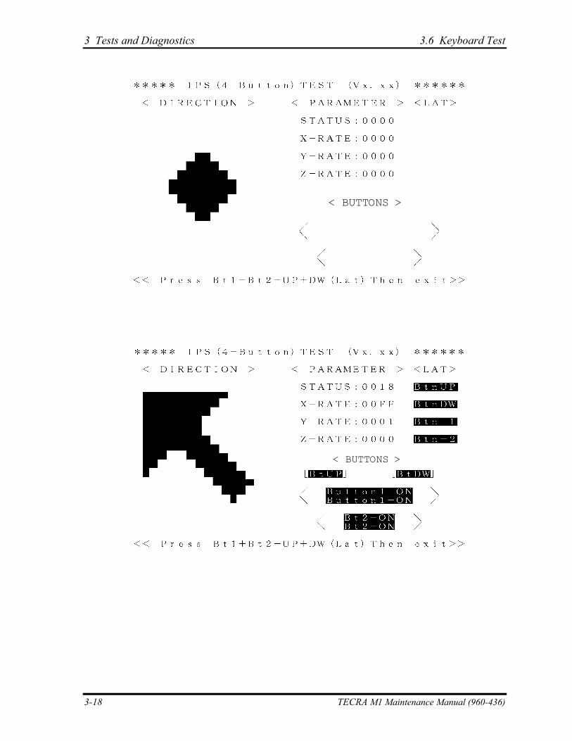
3 Tests and Diagnostics 3.6 Keyboard Test
< BUTTONS >
< BUTTONS >
3-18 TECRA M1 Maintenance Manual (960-436)
3.6 Keyboard Test 3 Tests and Diagnostics
To check only the USB mouse, follow the procedures below:
Connect the USB mouse to the computer’s USB connector.
Next, set up the computer’s hardware as follows:
PERIPHERAL
Internal Pointing Device = Simultaneous USB Legacy Emulation = Enabled
Then, perform the Pointing Stick Diagnostic Test and make sure:
• The cursor moves in the direction that you move the USB mouse. • The display reverses when you click the right button or left button
To stop this test, press the two IPS buttons on the computer at the same time. (You cannot use the USB mouse to stop the test.)
Subtest 05 USB Test
This Subtest checks USB. The USB TEST Module (ZD0003P01) and USB Cable (ZD0003P02) must be connected to the computer.
The following message will appear. Select a port to test and press Enter.
Test port number select (1:Port0, 2:Port1, 3:Port2) ?
If the test ends successfully, OK is displayed. If nothing is displayed, there may be a problem with the USB port. Check the wraparound connection and repeat the test.
Subtest 07 InTouch/Presentation key
When this subtest displays messages shown below in order, press the corresponding button.
NOTE: This subtest must be completed within 10 seconds. Press [ InTouch ] key Press [ Presentation ] key
TECRA M1 Maintenance Manual (960-436) 3-19
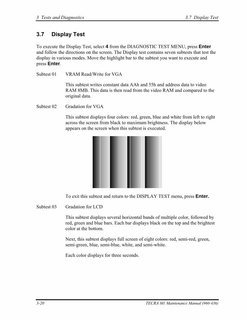
3 Tests and Diagnostics 3.7 Display Test
3.7 Display Test
To execute the Display Test, select 4 from the DIAGNOSTIC TEST MENU, press Enter and follow the directions on the screen. The Display test contains seven subtests that test the display in various modes. Move the highlight bar to the subtest you want to execute and press Enter.
Subtest 01 VRAM Read/Write for VGA
This subtest writes constant data AAh and 55h and address data to video RAM 8MB. This data is then read from the video RAM and compared to the original data.
Subtest 02 Gradation for VGA
This subtest displays four colors: red, green, blue and white from left to right across the screen from black to maximum brightness. The display below appears on the screen when this subtest is executed.
To exit this subtest and return to the DISPLAY TEST menu, press Enter.
Subtest 03 Gradation for LCD
This subtest displays several horizontal bands of multiple color, followed by red, green and blue bars. Each bar displays black on the top and the brightest color at the bottom.
Next, this subtest displays full screen of eight colors: red, semi-red, green, semi-green, blue, semi-blue, white, and semi-white.
Each color displays for three seconds.
3-20 TECRA M1 Maintenance Manual (960-436)
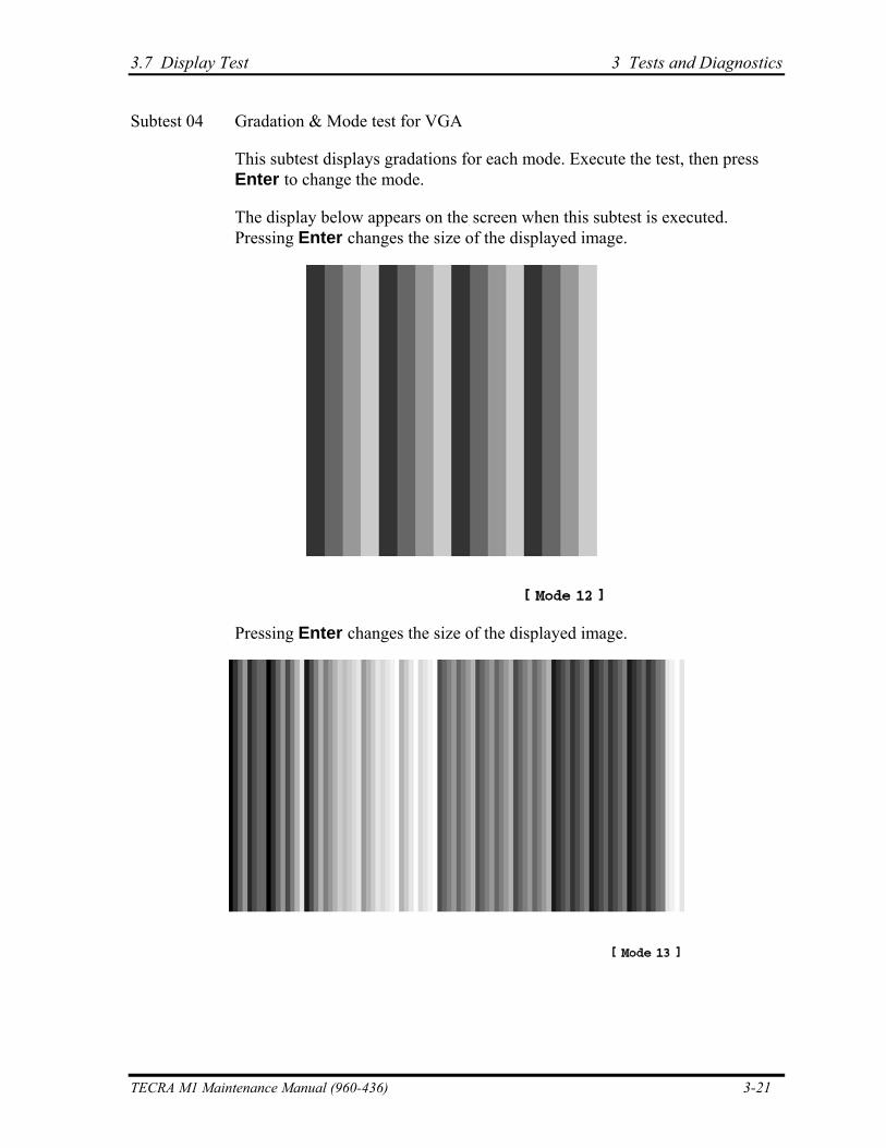
3.7 Display Test 3 Tests and Diagnostics
Subtest 04 Gradation & Mode test for VGA
This subtest displays gradations for each mode. Execute the test, then press Enter to change the mode.
The display below appears on the screen when this subtest is executed. Pressing Enter changes the size of the displayed image.
Pressing Enter changes the size of the displayed image.
TECRA M1 Maintenance Manual (960-436) 3-21
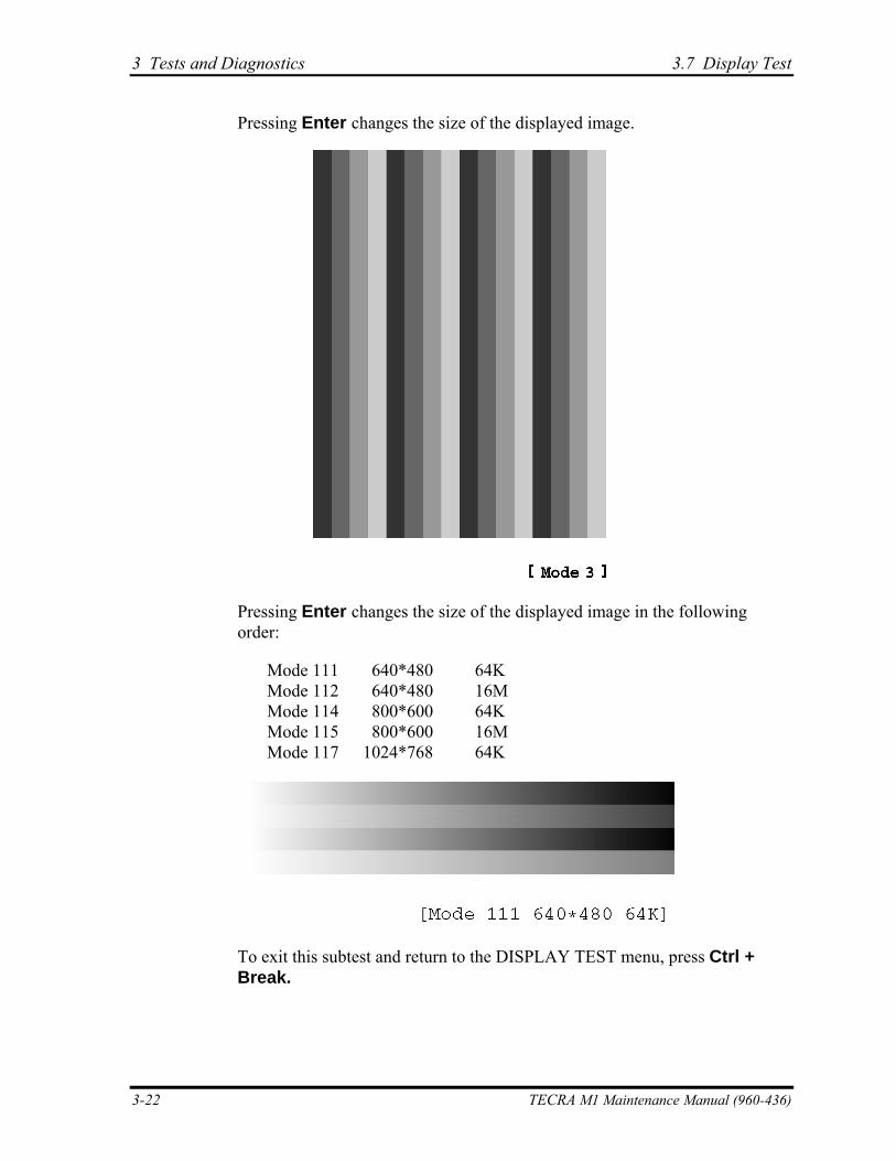
3 Tests and Diagnostics 3.7 Display Test
Pressing Enter changes the size of the displayed image.
Pressing Enter changes the size of the displayed image in the following order:
Mode 111 640*480 64K Mode 112 640*480 16M Mode 114 800*600 64K Mode 115 800*600 16M Mode 117 1024*768 64K
To exit this subtest and return to the DISPLAY TEST menu, press Ctrl + Break.
3-22 TECRA M1 Maintenance Manual (960-436)
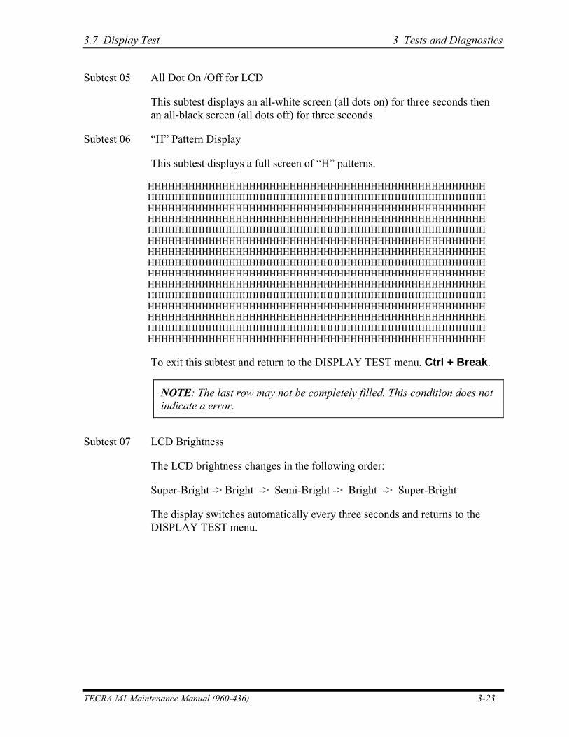
3.7 Display Test 3 Tests and Diagnostics
Subtest 05 All Dot On /Off for LCD
This subtest displays an all-white screen (all dots on) for three seconds then an all-black screen (all dots off) for three seconds.
Subtest 06 “H” Pattern Display
This subtest displays a full screen of “H” patterns.
HHHHHHHHHHHHHHHHHHHHHHHHHHHHHHHHHHHHHHHHHHHHHHHHHH HHHHHHHHHHHHHHHHHHHHHHHHHHHHHHHHHHHHHHHHHHHHHHHHHH HHHHHHHHHHHHHHHHHHHHHHHHHHHHHHHHHHHHHHHHHHHHHHHHHH HHHHHHHHHHHHHHHHHHHHHHHHHHHHHHHHHHHHHHHHHHHHHHHHHH HHHHHHHHHHHHHHHHHHHHHHHHHHHHHHHHHHHHHHHHHHHHHHHHHH HHHHHHHHHHHHHHHHHHHHHHHHHHHHHHHHHHHHHHHHHHHHHHHHHH HHHHHHHHHHHHHHHHHHHHHHHHHHHHHHHHHHHHHHHHHHHHHHHHHH HHHHHHHHHHHHHHHHHHHHHHHHHHHHHHHHHHHHHHHHHHHHHHHHHH HHHHHHHHHHHHHHHHHHHHHHHHHHHHHHHHHHHHHHHHHHHHHHHHHH HHHHHHHHHHHHHHHHHHHHHHHHHHHHHHHHHHHHHHHHHHHHHHHHHH HHHHHHHHHHHHHHHHHHHHHHHHHHHHHHHHHHHHHHHHHHHHHHHHHH HHHHHHHHHHHHHHHHHHHHHHHHHHHHHHHHHHHHHHHHHHHHHHHHHH HHHHHHHHHHHHHHHHHHHHHHHHHHHHHHHHHHHHHHHHHHHHHHHHHH HHHHHHHHHHHHHHHHHHHHHHHHHHHHHHHHHHHHHHHHHHHHHHHHHH HHHHHHHHHHHHHHHHHHHHHHHHHHHHHHHHHHHHHHHHHHHHHHHHHH
To exit this subtest and return to the DISPLAY TEST menu, Ctrl + Break.
NOTE: The last row may not be completely filled. This condition does not indicate a error.
Subtest 07 LCD Brightness
The LCD brightness changes in the following order:
Super-Bright -> Bright -> Semi-Bright -> Bright -> Super-Bright
The display switches automatically every three seconds and returns to the DISPLAY TEST menu.
TECRA M1 Maintenance Manual (960-436) 3-23
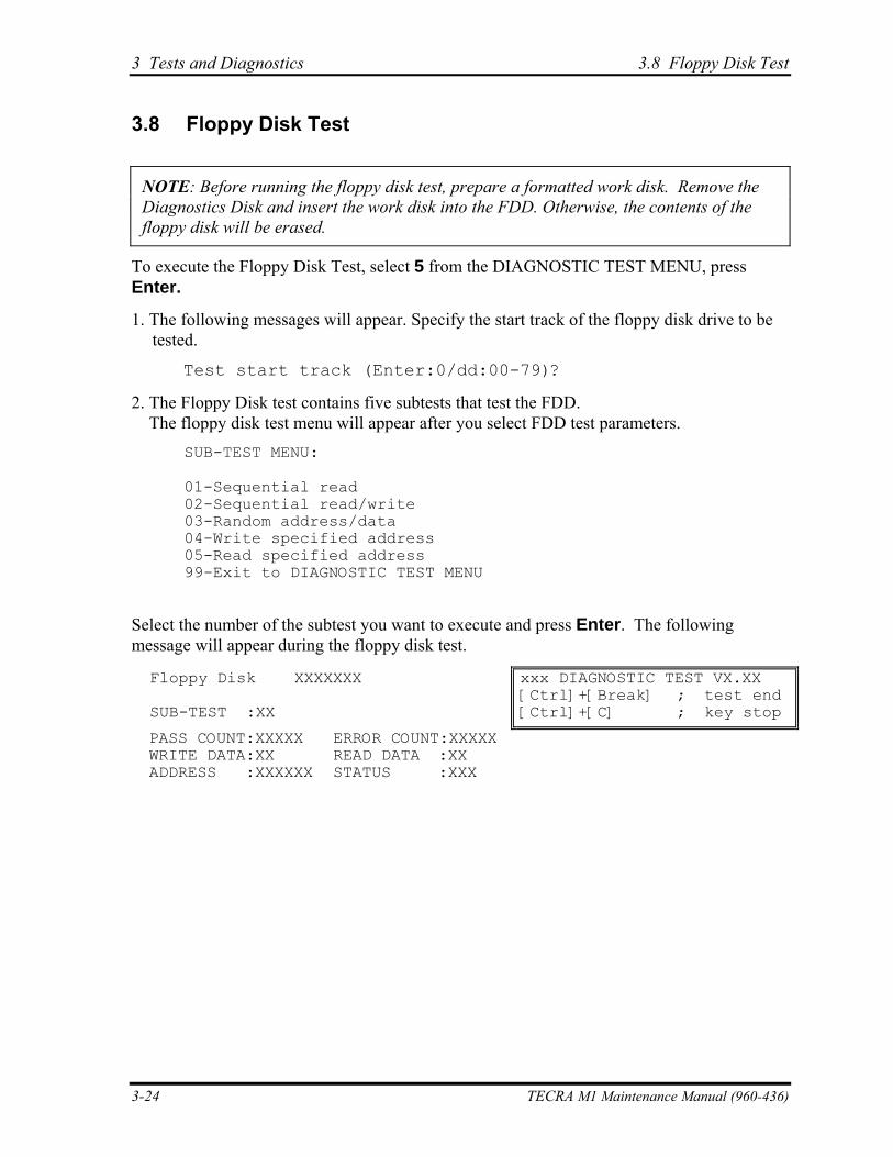
3 Tests and Diagnostics 3.8 Floppy Disk Test
3.8 Floppy Disk Test
NOTE: Before running the floppy disk test, prepare a formatted work disk. Remove the Diagnostics Disk and insert the work disk into the FDD. Otherwise, the contents of the floppy disk will be erased.
To execute the Floppy Disk Test, select 5 from the DIAGNOSTIC TEST MENU, press Enter.
1. The following messages will appear. Specify the start track of the floppy disk drive to be tested.
Test start track (Enter:0/dd:00-79)?
2. The Floppy Disk test contains five subtests that test the FDD. The floppy disk test menu will appear after you select FDD test parameters.
SUB-TEST MENU:
01-Sequential read 02-Sequential read/write 03-Random address/data 04-Write specified address 05-Read specified address 99-Exit to DIAGNOSTIC TEST MENU
Select the number of the subtest you want to execute and press Enter. The following message will appear during the floppy disk test.
Floppy Disk XXXXXXX SUB-TEST :XX
xxx DIAGNOSTIC TEST VX.XX [Ctrl]+[Break] ; test end [Ctrl]+[C] ; key stop
PASS COUNT:XXXXX ERROR COUNT:XXXXX WRITE DATA:XX READ DATA :XX ADDRESS :XXXXXX STATUS :XXX
3-24 TECRA M1 Maintenance Manual (960-436)
3.8 Floppy Disk Test 3 Tests and Diagnostics
Subtest 01 Sequential read
This subtest performs a Cyclic Redundancy Check (CRC) that continuously reads all the tracks (track: 0 to 39/0 to 79) on a floppy disk.
The start track is specified at the start of the FDD test. Refer to 1. in this section.
Subtest 02 Sequential read/write
This subtest continuously writes data pattern B5ADADh to all the tracks (track: 0 to 39/0 to 79) on a floppy disk. The data is then read and compared to the original data.
Subtest 03 Random address/data
This subtest writes random data to random addresses on all tracks (track: 0 to 39/0 to 79) on a floppy disk. The data is then read and compared to the original data.
Subtest 04 Write specified address
This subtest writes the data specified by an operator to a place pointed by track, head, and address.
Subtest 05 Read specified address
This subtest reads data from a place pointed by track, head, and address specified by an operator.
TECRA M1 Maintenance Manual (960-436) 3-25
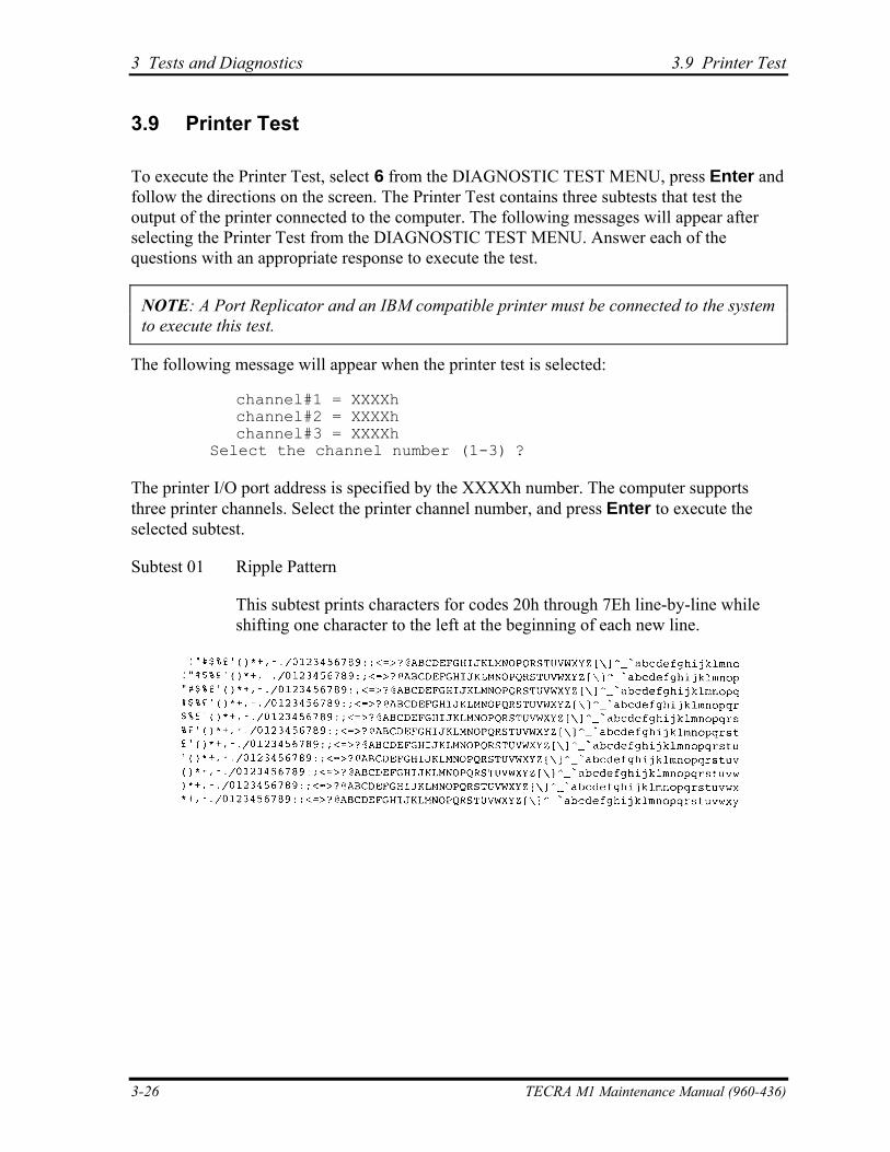
3 Tests and Diagnostics 3.9 Printer Test
3.9 Printer Test
To execute the Printer Test, select 6 from the DIAGNOSTIC TEST MENU, press Enter and follow the directions on the screen. The Printer Test contains three subtests that test the output of the printer connected to the computer. The following messages will appear after selecting the Printer Test from the DIAGNOSTIC TEST MENU. Answer each of the questions with an appropriate response to execute the test.
NOTE: A Port Replicator and an IBM compatible printer must be connected to the system to execute this test.
The following message will appear when the printer test is selected:
channel#1 = XXXXh channel#2 = XXXXh channel#3 = XXXXh
Select the channel number (1-3) ?
The printer I/O port address is specified by the XXXXh number. The computer supports three printer channels. Select the printer channel number, and press Enter to execute the selected subtest.
Subtest 01 Ripple Pattern
This subtest prints characters for codes 20h through 7Eh line-by-line while shifting one character to the left at the beginning of each new line.
3-26 TECRA M1 Maintenance Manual (960-436)
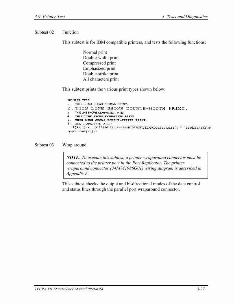
3.9 Printer Test 3 Tests and Diagnostics
Subtest 02 Function
This subtest is for IBM compatible printers, and tests the following functions:
Normal print Double-width print Compressed print Emphasized print Double-strike print All characters print
This subtest prints the various print types shown below:
Subtest 03 Wrap around
NOTE: To execute this subtest, a printer wraparound connector must be connected to the printer port in the Port Replicator. The printer wraparound connector (34M741986G01) wiring diagram is described in Appendix F.
This subtest checks the output and bi-directional modes of the data control and status lines through the parallel port wraparound connector.
TECRA M1 Maintenance Manual (960-436) 3-27
3 Tests and Diagnostics 3.10 Async Test
3.10 Async Test
To execute the Async Test, select 7 from the DIAGNOSTIC TEST MENU, press Enter and follow the directions displayed on the screen. The Async test contains two subtests that test the asynchronous communication functions. Move the highlight bar to the subtest you want to execute and press Enter.
Subtests require the following data format:
Method: Asynchronous Speed: 9600BPS (Subtests 01 to 04)
38400BPS (Subtests 06, 07) Data: 8 bits and one parity bit (EVEN) Data pattern: 20h to 7Eh
The following message will appear at the bottom of the screen when the subtest 01, 02 or 03 are selected.
Channel#1 = XXXXh Channel#2 = XXXXh Channel#3 = XXXXh Select the Channel number (1/2/3)
The serial I/O port address is specified by the XXXXh number. Select the serial port channel number and press Enter to start the subtest.
Subtest 01 Wraparound (board)
NOTE: To execute this subtest an RS-232C wraparound connector (34M741621G01) must be connected to the RS-232C port. The RS-232C wraparound connector wiring diagram is described in Appendix F.
This subtest checks the data send/receive function through the wraparound connector.
Subtest 02 Point to Point (send)
NOTE: To execute this subtest, two machines must be connected with an RS-232C direct cable. One machine should be set as “send”(subtest 02) and the other set as “receive” (subtest 03). The wiring diagram for the RS-232C direct cable is described in Appendix F.
This subtest sends 20h through 7Eh data to the receive side, then receives the sent data and compares it to the original data.
3-28 TECRA M1 Maintenance Manual (960-436)
3.10 Async Test 3 Tests and Diagnostics
Subtest 03 Point to Point (receive)
This subtest is used with subtest 02 described above. This subtest receives the data from the send side, then sends the received data.
Subtest 04 Interrupt Test
This subtest checks the Interrupt Request Level of IRQ 4, 3 and 5 from the send side.
Subtest 06 FIR/SIR Point to Point (send)
NOTE: To execute subtests 06 and 07, each computer must have access to the other computer’s infrared port.
This subtest sends 20h through 7Eh data to the receive side, then receives the sent data and compares it to the original data through the FIR/SIR port.
Subtest 07 FIR/SIR Point to Point (receive)
This subtest is used with subtest 06 described above. This subtest receives the data from the send side, then sends the received data through the FIR/SIR port.
TECRA M1 Maintenance Manual (960-436) 3-29
3 Tests and Diagnostics 3.11 Hard Disk Test
3.11 Hard Disk Test
To execute the Hard Disk Test, select 8 from the DIAGNOSTIC TEST MENU, press Enter, and follow the directions on the screen. The hard disk test contains ten subtests that test the hard disk drive functions.
NOTE: To execute the subtest 02,03,04,06,09 or 10, the system requires you to enter password. The contents of the hard disk will be erased when the subtest 02, 03, 04, 06,09, or 10 is executed. Before running the test, the customer should transfer the contents of the hard disk to floppy disk. If the customer has not or cannot perform the back-up, create back-up disks as described below.
Check to see if the Microsoft Create System Disks Tools (MSCSD.EXE) still exists in the System Tools Folder. (This tool can be used only once.) If it exists, use it to back up the pre-installed software, then use the Backup utility in the System Tools folder to back up the entire disk, including the user’s files.
Refer to the operating system instructions.
After selecting the hard disk test from the DIAGNOSTIC TEST MENU, answer each of the questions with an appropriate response to execute the test.
1. Select the hard disk drive number to be tested.
Test drive number select (1:HDD#1, 2:HDD#2, 0:HDD1&2)
2. This message is used to select the retry operation when the hard disk controller detects an error. Select yes or no.
HDC F/W error retry (1:yes, 2:no) ?
3. This message is used to select the error dump operation when a data compare error is detected. Select yes or no.
Data compare error dump (1:no, 2:yes) ?
4. This message is used to select whether or not the HDD status is displayed on the screen. The HDD status is described in section 3.19. Select yes or no.
Detail status display (1:no, 2:yes) ?
5. The Hard Disk Test message will appear after you respond to the Detail Status prompt. Select the number of the subtest you want to execute and press Enter. The following message will appear during each subtest.
3-30 TECRA M1 Maintenance Manual (960-436)
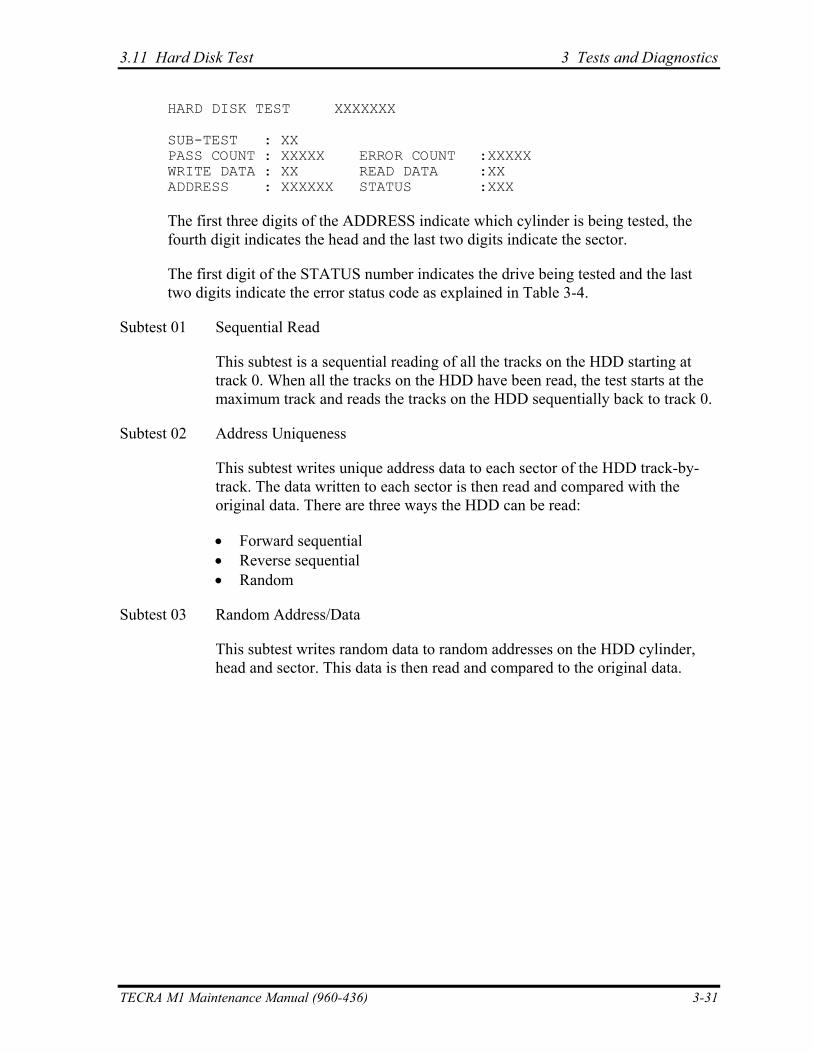
3.11 Hard Disk Test 3 Tests and Diagnostics
HARD DISK TEST XXXXXXX
SUB-TEST : XX PASS COUNT : XXXXX ERROR COUNT :XXXXX WRITE DATA : XX READ DATA :XX ADDRESS : XXXXXX STATUS :XXX
The first three digits of the ADDRESS indicate which cylinder is being tested, the fourth digit indicates the head and the last two digits indicate the sector.
The first digit of the STATUS number indicates the drive being tested and the last two digits indicate the error status code as explained in Table 3-4.
Subtest 01 Sequential Read
This subtest is a sequential reading of all the tracks on the HDD starting at track 0. When all the tracks on the HDD have been read, the test starts at the maximum track and reads the tracks on the HDD sequentially back to track 0.
Subtest 02 Address Uniqueness
This subtest writes unique address data to each sector of the HDD track-by-track. The data written to each sector is then read and compared with the original data. There are three ways the HDD can be read:
• Forward sequential • Reverse sequential • Random
Subtest 03 Random Address/Data
This subtest writes random data to random addresses on the HDD cylinder, head and sector. This data is then read and compared to the original data.
TECRA M1 Maintenance Manual (960-436) 3-31
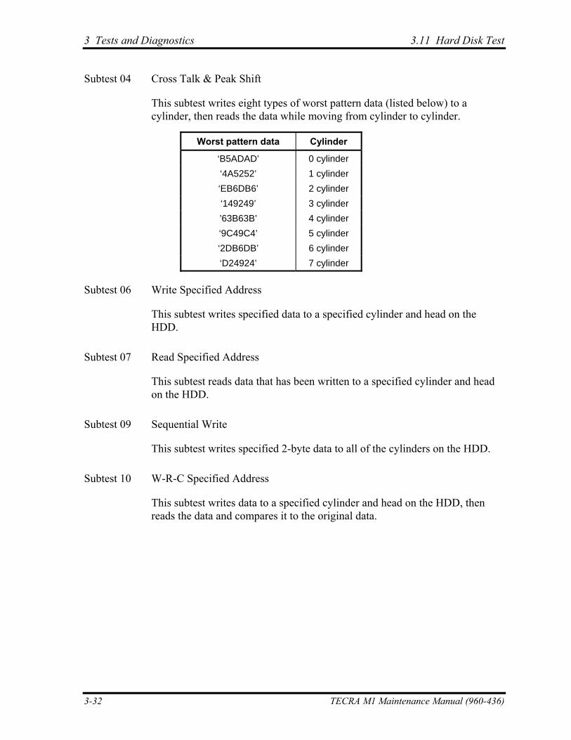
3 Tests and Diagnostics 3.11 Hard Disk Test
Subtest 04 Cross Talk & Peak Shift
This subtest writes eight types of worst pattern data (listed below) to a cylinder, then reads the data while moving from cylinder to cylinder.
Worst pattern data Cylinder
‘B5ADAD’ 0 cylinder ‘4A5252’ 1 cylinder ‘EB6DB6’ 2 cylinder ‘149249’ 3 cylinder ’63B63B’ 4 cylinder
‘9C49C4’ 5 cylinder
‘2DB6DB’ 6 cylinder
‘D24924’ 7 cylinder
Subtest 06 Write Specified Address
This subtest writes specified data to a specified cylinder and head on the HDD.
Subtest 07 Read Specified Address
This subtest reads data that has been written to a specified cylinder and head on the HDD.
Subtest 09 Sequential Write
This subtest writes specified 2-byte data to all of the cylinders on the HDD.
Subtest 10 W-R-C Specified Address
This subtest writes data to a specified cylinder and head on the HDD, then reads the data and compares it to the original data.
3-32 TECRA M1 Maintenance Manual (960-436)
3.12 Real Timer Test 3 Tests and Diagnostics
3.12 Real Timer Test
To execute the Real Timer Test, select 9 from the DIAGNOSTIC TEST MENU, press Enter and follow the directions on the screen. The real timer test contains three Subtests that test the computer’s real timer functions. Move the highlight bar to the Subtest you want to execute and press Enter.
Subtest 01 Real Time
A new date and time can be input during this Subtest. To execute the real time subtest follow these steps:
1. Select the subtest 01 and the following message will appear:
Current date : XX-XX-XXXX Current time : XX:XX:XX
Enter new date:
PRESS [ENTER] KEY TO EXIT TEST
2. If the current date is not correct, input the correct date at the “Enter new date” prompt and press Enter. To enter “:”, press Shift + ;. The date is updated and the following prompt will appear:
Enter new time :
3. If the current time is not correct, input the correct time in 24-hour format and press Enter. The time is updated.
Subtest 02 Backup Memory
This Subtest performs the following backup memory check:
Writes 1-bit of “on” data to address 01h through 80h Writes 1-bit of “off” data to address 0Eh through 80h Writes the data pattern AAh and 55h to the RTC 114-byte memory (address 0Eh to 7Fh)
The Subtest reads and compares this data with the original data.
To exit, press Ctrl + Break.
TECRA M1 Maintenance Manual (960-436) 3-33
3 Tests and Diagnostics 3.12 Real Timer Test
Subtest 03 Real Time Carry
CAUTION: When you execute this Subtest, the current date and time are erased.
This Subtest checks the real time clock increments, making sure the date and time are displayed in the following format:
Current date : 12-31-2001 Current time : 23:59:58
PRESS [Enter] KEY TO EXIT TEST
Press Enter to exit.
3-34 TECRA M1 Maintenance Manual (960-436)
3.13 NDP Test 3 Tests and Diagnostics
3.13 NDP Test
To execute the NDP test, select 10 from the DIAGNOSTICS TEST MENU, press Enter and follow the directions on the screen. The NDP test contains one Subtest that tests the computer’s NDP functions.
Subtest 01 NDP
This test checks the following functions of the coprocessor:
Control word
Status word
Bus
Addition
Multiplication
Press Ctrl + Break to exit.
TECRA M1 Maintenance Manual (960-436) 3-35
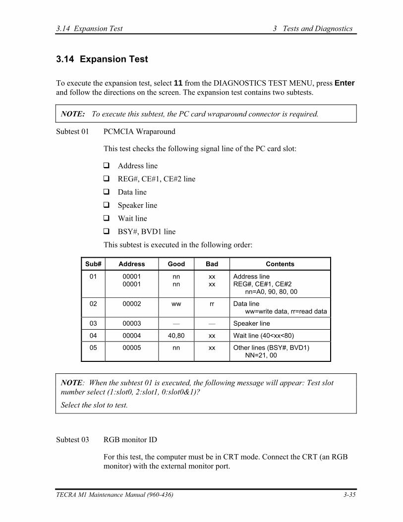
3.14 Expansion Test 3 Tests and Diagnostics
3
3.14 Expansion Test
To execute the expansion test, select 11 from the DIAGNOSTICS TEST MENU, press Enter and follow the directions on the screen. The expansion test contains two subtests.
NOTE: To execute this subtest, the PC card wraparound connector is required.
Subtest 01 PCMCIA Wraparound
This test checks the following signal line of the PC card slot:
Address line
REG#, CE#1, CE#2 line
Data line
Speaker line
Wait line
BSY#, BVD1 line
This subtest is executed in the following order:
Sub# Address Good Bad Contents
01 00001 00001
nn nn
xx xx
Address line REG#, CE#1, CE#2 nn=A0, 90, 80, 00
02 00002 ww rr Data line ww=write data, rr=read data
03 00003 –– –– Speaker line
04 00004 40,80 xx Wait line (40<xx<80)
05 00005 nn xx Other lines (BSY#, BVD1) NN=21, 00
NOTE: When the subtest 01 is executed, the following message will appear: Test slot number select (1:slot0, 2:slot1, 0:slot0&1)?
Select the slot to test.
Subtest 03 RGB monitor ID
For this test, the computer must be in CRT mode. Connect the CRT (an RGB monitor) with the external monitor port.
TECRA M1 Maintenance Manual (960-436) 3-35
3 Tests and Diagnostics 3.15 CD-ROM/DVD-ROM Test
3.15 CD-ROM/DVD-ROM Test
To execute the CD-ROM/DVD-ROM test, select 13 from the DIAGNOSTICS TEST MENU, press Enter and follow the directions on the screen. The CD-ROM/DVD-ROM test contains six Subtests that test the computer’s CD-ROM/DVD-ROM functions.
NOTE: Make sure the CD-ROM driver (CDRNEW.COM) is installed and insert the test menu media CD (TOSHIBA CD-ROM TEST DISK (ZA1217P01/P000204190)). For the DVD-DOM test, insert the media CD (Toshiba-EMI TEST DISK TSD-1).
Subtest 01 Sequential Read
This Subtest is a sequential reading of one-block units (2K bytes) of all the logical addresses.
Subtest 02 Read Specified Address
This Subtest reads one-block data from a specified address.
Subtest 03 Random Address/Data
This Subtest reads one-block data and multi-block data from random addresses 200 times.
Subtest 04 Playback Music (CD only)
NOTE: You cannot use the Toshiba-EMI DVD-ROM TEST DISK TSD-1 for Subtest 04. For this test, use an ordinary music CD.
This Subtest reads track data from a specified track and plays the sound.
Subtest 05 RW 1 point W/R/C
This subtest performs the CD-RW drive test.
NOTE: For the CD-RW drive test, use CD-RW media that supports four-speed writing (media manufactured by RICOH or Mitsubishi Chemical are recommended.)
3-36 TECRA M1 Maintenance Manual (960-436)
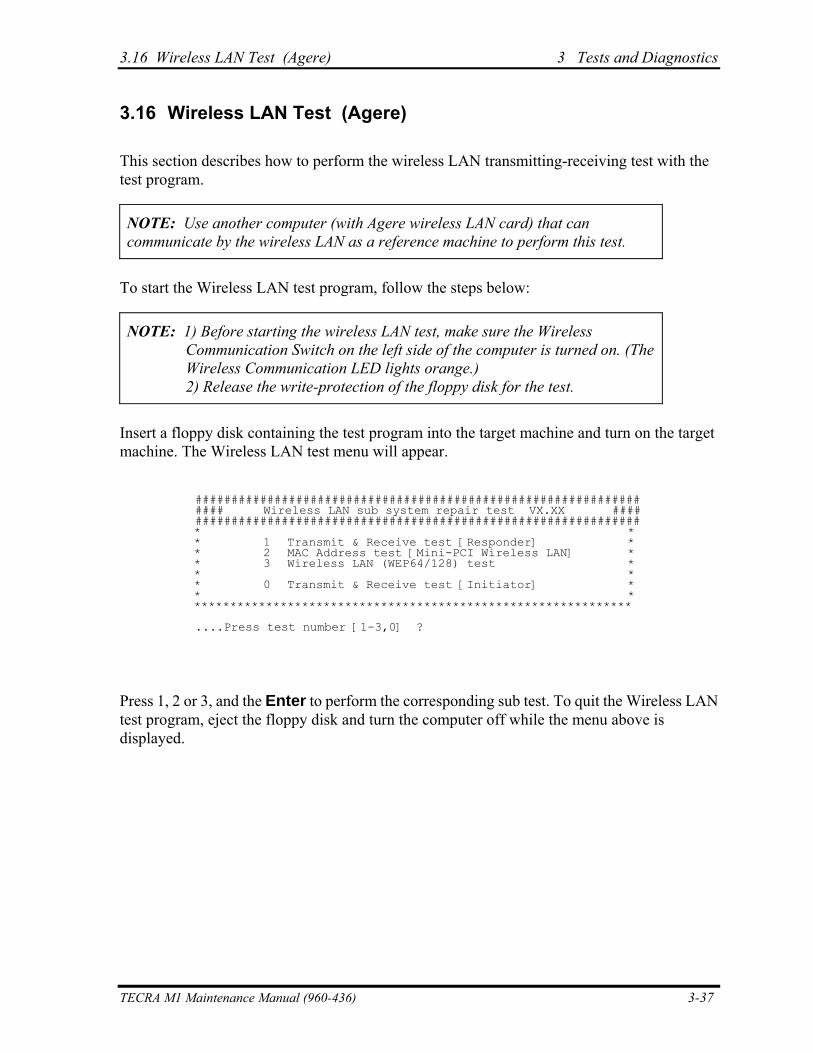
3.16 Wireless LAN Test (Agere) 3 Tests and Diagnostics
3.16 Wireless LAN Test (Agere)
This section describes how to perform the wireless LAN transmitting-receiving test with the test program.
NOTE: Use another computer (with Agere wireless LAN card) that can communicate by the wireless LAN as a reference machine to perform this test.
To start the Wireless LAN test program, follow the steps below:
NOTE: 1) Before starting the wireless LAN test, make sure the Wireless Communication Switch on the left side of the computer is turned on. (The Wireless Communication LED lights orange.) 2) Release the write-protection of the floppy disk for the test.
Insert a floppy disk containing the test program into the target machine and turn on the target machine. The Wireless LAN test menu will appear.
############################################################## #### Wireless LAN sub system repair test VX.XX #### ############################################################## * * * 1 Transmit & Receive test [Responder] * * 2 MAC Address test [Mini-PCI Wireless LAN] * * 3 Wireless LAN (WEP64/128) test * * * * 0 Transmit & Receive test [Initiator] * * * ************************************************************* ....Press test number [1-3,0] ?
Press 1, 2 or 3, and the Enter to perform the corresponding sub test. To quit the Wireless LAN test program, eject the floppy disk and turn the computer off while the menu above is displayed.
TECRA M1 Maintenance Manual (960-436) 3-37
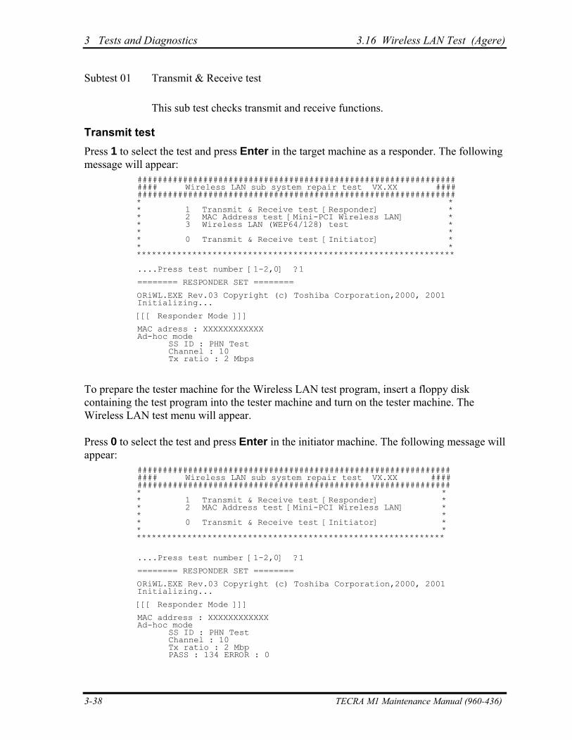
3 Tests and Diagnostics 3.16 Wireless LAN Test (Agere)
Subtest 01 Transmit & Receive test
This sub test checks transmit and receive functions.
Transmit test Press 1 to select the test and press Enter in the target machine as a responder. The following message will appear:
############################################################### #### Wireless LAN sub system repair test VX.XX #### ############################################################### * * * 1 Transmit & Receive test [Responder] * * 2 MAC Address test [Mini-PCI Wireless LAN] * * 3 Wireless LAN (WEP64/128) test * * * * 0 Transmit & Receive test [Initiator] * * * *************************************************************** ....Press test number [1-2,0] ?1
======== RESPONDER SET ========
ORiWL.EXE Rev.03 Copyright (c) Toshiba Corporation,2000, 2001 Initializing...
[[[ Responder Mode ]]]
MAC adress : XXXXXXXXXXXX Ad-hoc mode SS ID : PHN Test Channel : 10 Tx ratio : 2 Mbps
To prepare the tester machine for the Wireless LAN test program, insert a floppy disk containing the test program into the tester machine and turn on the tester machine. The Wireless LAN test menu will appear. Press 0 to select the test and press Enter in the initiator machine. The following message will appear:
############################################################## #### Wireless LAN sub system repair test VX.XX #### ############################################################## * * * 1 Transmit & Receive test [Responder] * * 2 MAC Address test [Mini-PCI Wireless LAN] * * * * 0 Transmit & Receive test [Initiator] * * * *************************************************************
....Press test number [1-2,0] ?1
======== RESPONDER SET ========
ORiWL.EXE Rev.03 Copyright (c) Toshiba Corporation,2000, 2001 Initializing...
[[[ Responder Mode ]]]
MAC address : XXXXXXXXXXXX Ad-hoc mode SS ID : PHN Test Channel : 10 Tx ratio : 2 Mbp PASS : 134 ERROR : 0
3-38 TECRA M1 Maintenance Manual (960-436)
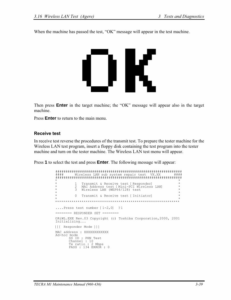
3.16 Wireless LAN Test (Agere) 3 Tests and Diagnostics
When the machine has passed the test, “OK” message will appear in the test machine.
Then press Enter in the target machine; the “OK” message will appear also in the target machine.
Press Enter to return to the main menu.
Receive test In receive test reverse the procedures of the transmit test. To prepare the tester machine for the Wireless LAN test program, insert a floppy disk containing the test program into the tester machine and turn on the tester machine. The Wireless LAN test menu will appear. Press 1 to select the test and press Enter. The following message will appear:
############################################################## #### Wireless LAN sub system repair test VX.XX #### ############################################################## * * * 1 Transmit & Receive test [Responder] * * 2 MAC Address test [Mini-PCI Wireless LAN] * * 3 Wireless LAN (WEP64/128) test * * * * 0 Transmit & Receive test [Initiator] * * * ************************************************************* ....Press test number [1-2,0] ?1
======== RESPONDER SET ========
ORiWL.EXE Rev.03 Copyright (c) Toshiba Corporation,2000, 2001 Initializing...
[[[ Responder Mode ]]]
MAC address : XXXXXXXXXXXX Ad-hoc mode SS ID : PHN Test Channel : 10 Tx ratio : 2 Mbps PASS : 134 ERROR : 0
TECRA M1 Maintenance Manual (960-436) 3-39
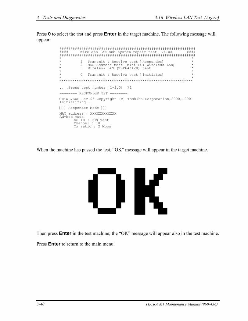
3 Tests and Diagnostics 3.16 Wireless LAN Test (Agere)
Press 0 to select the test and press Enter in the target machine. The following message will appear:
############################################################## #### Wireless LAN sub system repair test VX.XX #### ############################################################## * * * 1 Transmit & Receive test [Responder] * * 2 MAC Address test [Mini-PCI Wireless LAN] * * 3 Wireless LAN (WEP64/128) test * * * * 0 Transmit & Receive test [Initiator] * * * ************************************************************* ....Press test number [1-2,0] ?1
======== RESPONDER SET ========
ORiWL.EXE Rev.03 Copyright (c) Toshiba Corporation,2000, 2001 Initializing...
[[[ Responder Mode ]]]
MAC address : XXXXXXXXXXXX Ad-hoc mode SS ID : PHN Test Channel : 10 Tx ratio : 2 Mbps
When the machine has passed the test, “OK” message will appear in the target machine.
Then press Enter in the test machine; the “OK” message will appear also in the test machine.
Press Enter to return to the main menu.
3-40 TECRA M1 Maintenance Manual (960-436)
3.16 Wireless LAN Test (Agere) 3 Tests and Diagnostics
Subtest 02 Mac Address test
This subtest reads MAC Address. If there is no problem, the “OK” message will appear.
Subtest 03 Wireless LAN (WEP64/128) test
This subtest reads the WEP of the wireless LAN card installed in the target machine. A message similar to the following will appear:
****** This CARD is WEP ****** Press any key to continue
TECRA M1 Maintenance Manual (960-436) 3-41
3 Tests and Diagnostics 3.17 Wireless LAN Test (Atheros)
3.17 Wireless LAN Test (Atheros)
This section describes how to perform the wireless LAN transmitting-receiving test with the test program.
NOTE: Use another computer (with Atheros wireless LAN card) that can communicate by the wireless LAN as a responder machine to perform this test.
In this test, the following items are tested:
* Test PC [Initiator] side (1) SKU (destination code) check (2) Mac Address check (3) Communication test (802.11a Main antenna) (4) Communication test (802.11a Sub antenna) (5) Communication test (802.11b)
* [Responder] side (1) Communication test (802.11b)
This program conducts the above test items continuously and displays results for each item during the test. However, only the last result for the whole test shall be checked. (The message "OK" or "NG" is displayed.)
When an "NG" item is detected during the test, the message "NG" is displayed on the screen and the test stops.
NOTE: This program takes a long time until the test ends.
To start the Wireless LAN test program, follow the steps below:
NOTE: Before starting the wireless LAN test, make sure the Wireless Communication Switch on the left side of the computer is turned on. (The Wireless Communication LED lights orange.)
3-42 TECRA M1 Maintenance Manual (960-436)
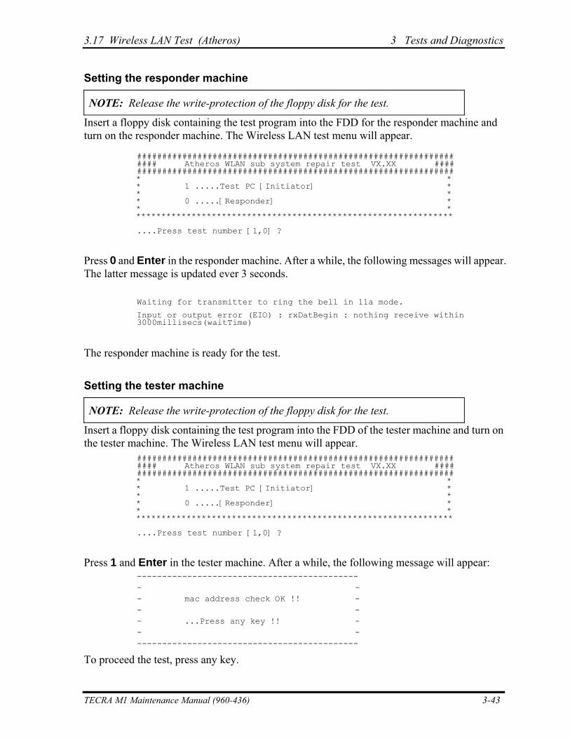
3.17 Wireless LAN Test (Atheros) 3 Tests and Diagnostics
Setting the responder machine
NOTE: Release the write-protection of the floppy disk for the test.
Insert a floppy disk containing the test program into the FDD for the responder machine and turn on the responder machine. The Wireless LAN test menu will appear.
############################################################### #### Atheros WLAN sub system repair test VX.XX #### ############################################################### * * * 1 .....Test PC [Initiator] * * * * 0 .....[Responder] * * * *************************************************************** ....Press test number [1,0] ?
Press 0 and Enter in the responder machine. After a while, the following messages will appear. The latter message is updated ever 3 seconds.
Waiting for transmitter to ring the bell in 11a mode.
Input or output error (EIO) : rxDatBegin : nothing receive within 3000millisecs(waitTime)
The responder machine is ready for the test.
Setting the tester machine
NOTE: Release the write-protection of the floppy disk for the test.
Insert a floppy disk containing the test program into the FDD of the tester machine and turn on the tester machine. The Wireless LAN test menu will appear.
############################################################### #### Atheros WLAN sub system repair test VX.XX #### ############################################################### * * * 1 .....Test PC [Initiator] * * * * 0 .....[Responder] * * * *************************************************************** ....Press test number [1,0] ?
Press 1 and Enter in the tester machine. After a while, the following message will appear:
-------------------------------------------- - - - mac address check OK !! - - - - ...Press any key !! - - - --------------------------------------------
To proceed the test, press any key.
TECRA M1 Maintenance Manual (960-436) 3-43
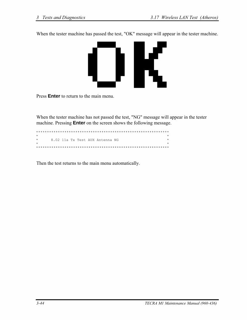
3 Tests and Diagnostics 3.17 Wireless LAN Test (Atheros)
When the tester machine has passed the test, "OK" message will appear in the tester machine.
Press Enter to return to the main menu.
When the tester machine has not passed the test, "NG" message will appear in the tester machine. Pressing Enter on the screen shows the following message.
************************************************************* * * * 8.02 11a Tx Test AUX Antenna NG * * * *************************************************************
Then the test returns to the main menu automatically.
3-44 TECRA M1 Maintenance Manual (960-436)
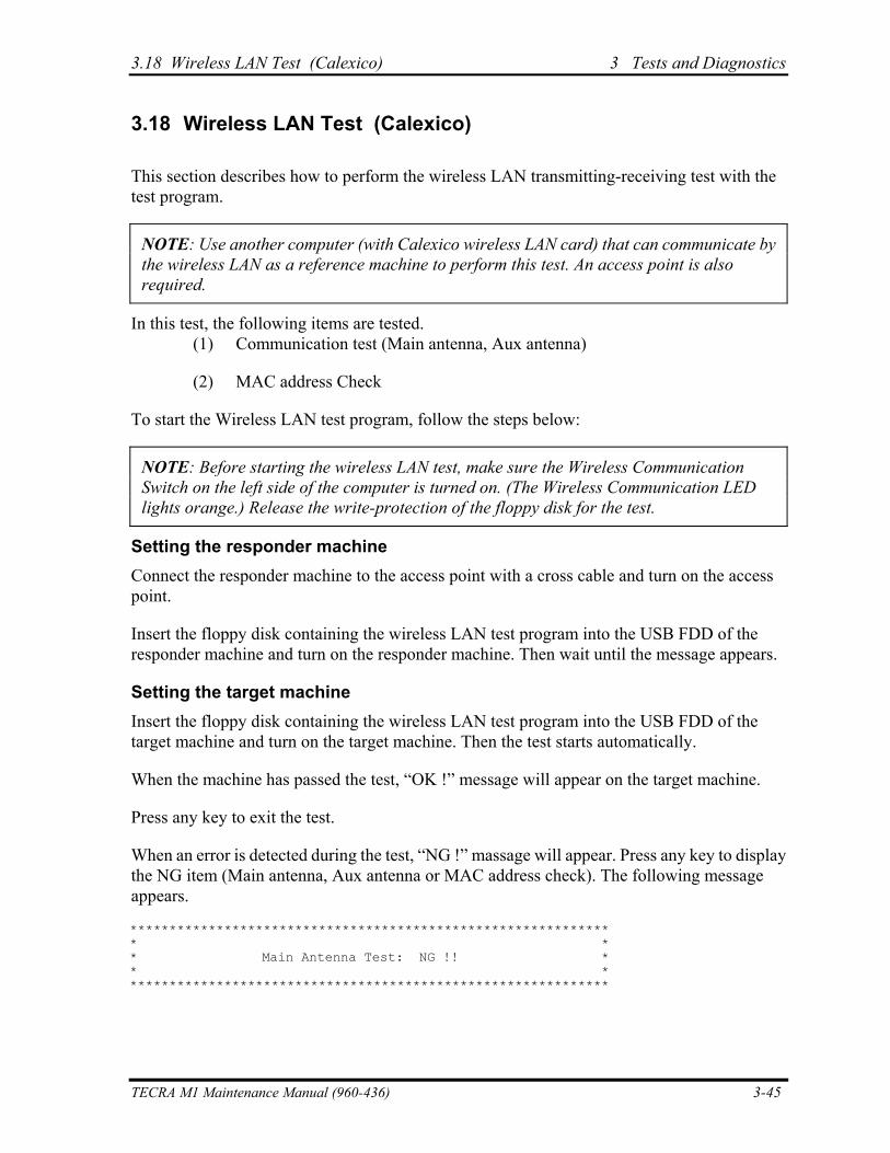
3.18 Wireless LAN Test (Calexico) 3 Tests and Diagnostics
3.18 Wireless LAN Test (Calexico)
This section describes how to perform the wireless LAN transmitting-receiving test with the test program.
NOTE: Use another computer (with Calexico wireless LAN card) that can communicate by the wireless LAN as a reference machine to perform this test. An access point is also required.
In this test, the following items are tested. (1) Communication test (Main antenna, Aux antenna)
(2) MAC address Check
To start the Wireless LAN test program, follow the steps below:
NOTE: Before starting the wireless LAN test, make sure the Wireless Communication Switch on the left side of the computer is turned on. (The Wireless Communication LED lights orange.) Release the write-protection of the floppy disk for the test.
Setting the responder machine Connect the responder machine to the access point with a cross cable and turn on the access point.
Insert the floppy disk containing the wireless LAN test program into the USB FDD of the responder machine and turn on the responder machine. Then wait until the message appears.
Setting the target machine Insert the floppy disk containing the wireless LAN test program into the USB FDD of the target machine and turn on the target machine. Then the test starts automatically.
When the machine has passed the test, “OK !” message will appear on the target machine.
Press any key to exit the test.
When an error is detected during the test, “NG !” massage will appear. Press any key to display the NG item (Main antenna, Aux antenna or MAC address check). The following message appears.
************************************************************* * * * Main Antenna Test: NG !! * * * *************************************************************
TECRA M1 Maintenance Manual (960-436) 3-45
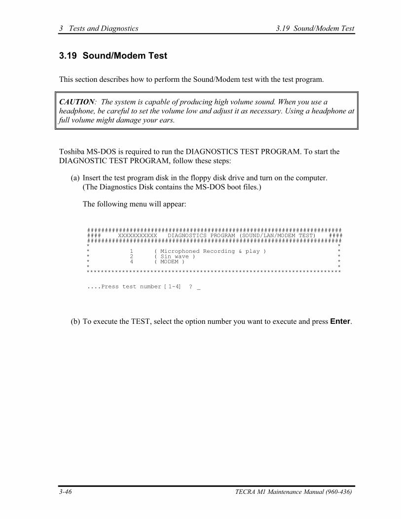
3 Tests and Diagnostics 3.19 Sound/Modem Test
3.19 Sound/Modem Test
This section describes how to perform the Sound/Modem test with the test program.
CAUTION: The system is capable of producing high volume sound. When you use a headphone, be careful to set the volume low and adjust it as necessary. Using a headphone at full volume might damage your ears.
Toshiba MS-DOS is required to run the DIAGNOSTICS TEST PROGRAM. To start the DIAGNOSTIC TEST PROGRAM, follow these steps:
(a) Insert the test program disk in the floppy disk drive and turn on the computer. (The Diagnostics Disk contains the MS-DOS boot files.)
The following menu will appear:
######################################################################## #### XXXXXXXXXXX DIAGNOSTICS PROGRAM (SOUND/LAN/MODEM TEST) #### ######################################################################## * * * 1 ( Microphoned Recording & play ) * * 2 ( Sin wave ) * * 4 ( MODEM ) * * * ************************************************************************
....Press test number [1-4] ? _
(b) To execute the TEST, select the option number you want to execute and press Enter.
3-46 TECRA M1 Maintenance Manual (960-436)
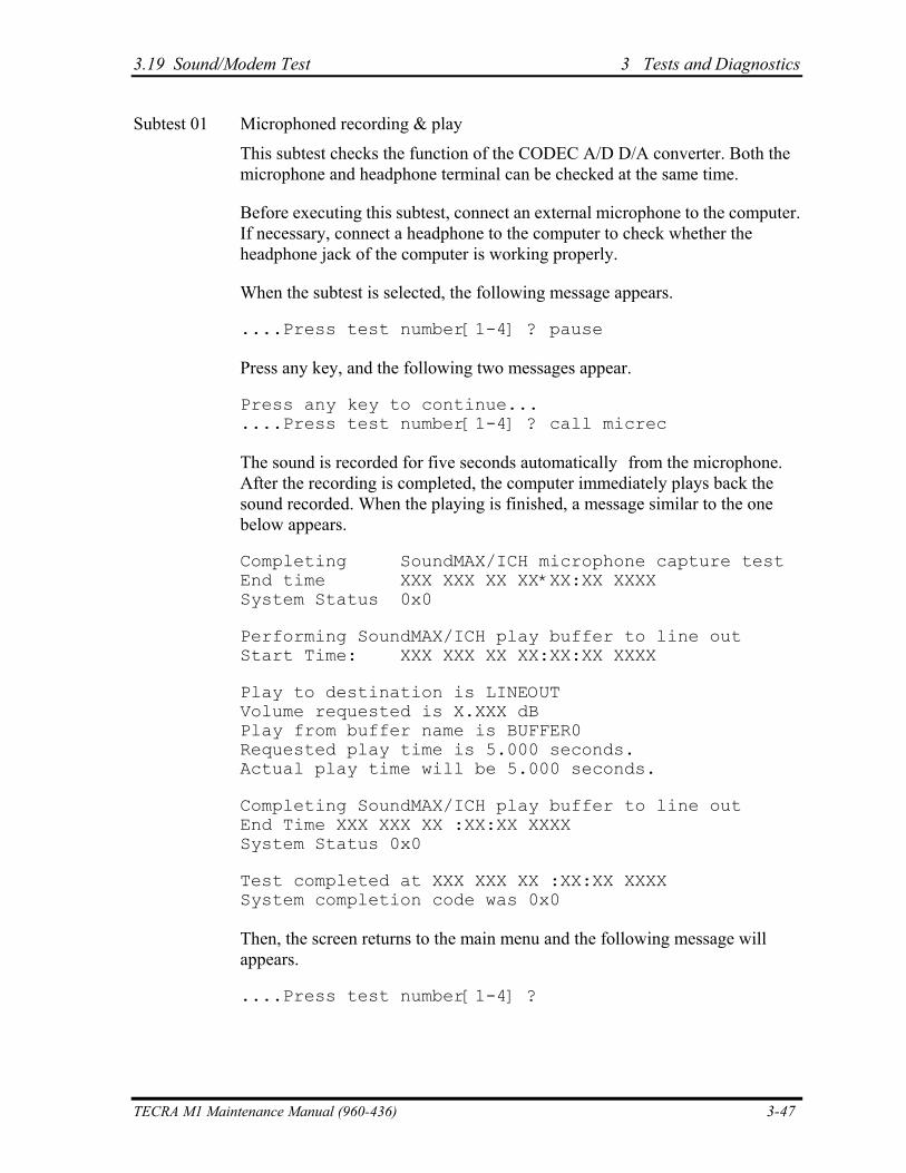
3.19 Sound/Modem Test 3 Tests and Diagnostics
Subtest 01 Microphoned recording & play
This subtest checks the function of the CODEC A/D D/A converter. Both the microphone and headphone terminal can be checked at the same time.
Before executing this subtest, connect an external microphone to the computer. If necessary, connect a headphone to the computer to check whether the headphone jack of the computer is working properly.
When the subtest is selected, the following message appears.
....Press test number[1-4] ? pause
Press any key, and the following two messages appear.
Press any key to continue... ....Press test number[1-4] ? call micrec
The sound is recorded for five seconds automatically from the microphone. After the recording is completed, the computer immediately plays back the sound recorded. When the playing is finished, a message similar to the one below appears.
Completing SoundMAX/ICH microphone capture test End time XXX XXX XX XX*XX:XX XXXX System Status 0x0
Performing SoundMAX/ICH play buffer to line out Start Time: XXX XXX XX XX:XX:XX XXXX
Play to destination is LINEOUT Volume requested is X.XXX dB Play from buffer name is BUFFER0 Requested play time is 5.000 seconds. Actual play time will be 5.000 seconds.
Completing SoundMAX/ICH play buffer to line out End Time XXX XXX XX :XX:XX XXXX System Status 0x0
Test completed at XXX XXX XX :XX:XX XXXX System completion code was 0x0
Then, the screen returns to the main menu and the following message will appears.
....Press test number[1-4] ?
TECRA M1 Maintenance Manual (960-436) 3-47
3 Tests and Diagnostics 3.19 Sound/Modem Test
To execute a subtest continuously, select the test number and press Enter. To exit the Sound/LAN/Modem test, remove the test program disk from the USB FDD and turn the computer off.
Subtest 02 Sin Wave
This subtest is executed by the load format of COM file (ADSIN.COM). The program expands sin wave data table to data in 16-64KB, and creates play data (It sounds like continuous beep). By using wave measuring devices such as an oscilloscope, this program can read sine wave without expanding.
When the subtest is executed, the following message appears.
....Press test number[1-4] ? pause Press any key to continue...
Press any key, and the following message appears. Then sin wave is expanded to 16-64KB data and is played.
....Press test number[1-4] ? call sin
When the beep sound finished, the screen returns to the main menu and the following massage appears.
....Press test number [1-4] ?
To execute a subtest continuously, select the test number and press Enter. To exit the Sound/Modem test, remove the test program disk from the USB FDD and turn the computer off.
3-48 TECRA M1 Maintenance Manual (960-436)
3.19 Sound/Modem Test 3 Tests and Diagnostics
Subtest 04 Modem Test
(a) Select 4 to execute and press Enter. The following message will appear:
ICHX MDC Test Program with Modem Sound ( PCB Interface ) Version X.X
* Scorpio Modem Initialize :OK
* Digital Loopback Test :OK
* Modem Sound Test :( Operator’s Check!! )
(b) After a few seconds, the following message will appear:
...Press Key ( Y = OK , N =NG )
If you hear the modem sound from the speakers, press Y. Otherwise, press N.
NOTE: The menu displayed by your computer may be slightly different from the one shown above.
(c) After you press Y or N, the RJ11 Connection Check (LED) ((Operator’s Check LED)) test will execute, and the following message will appear:
...Press Key ( Y = OK , N =NG )
If the color in the LED of the connection checker is orange, press Y. Otherwise, press N.
Press Enter to return to Main Menu.
TECRA M1 Maintenance Manual (960-436) 3-49
3 Tests and Diagnostics 3.20 IEEE1394 Test Program
3.20 IEEE1394 Test Program
This section describes how to perform the IEEE1394 test with the test program.
Toshiba MS-DOS is required to run the DIAGNOSTICS TEST PROGRAM. To start the DIAGNOSTIC TEST PROGRAM, follow these steps:
(a) Insert the Diagnostics disk in the floppy disk drive and turn on the computer. (The Diagnostics Disk contains the MS-DOS boot files.)
The following menu will appear:
*********************************************************************** * ------------------------------------------------------------ * * IEEE1394 [TSB!”LV28] test menu ( For Repair ) VX.XX * * ------------------------------------------------------------ * * * * ============ Select test No. and [Enter] ============ * * * * 1 : ... Ieee1384 test * * 2 : ... Responder tool * * 3 : ... ID Check * * * ***********************************************************************
Select [1-3]?
(b) To execute the TEST, select the test number you want to execute and press Enter.
3-50 TECRA M1 Maintenance Manual (960-436)
3.20 IEEE1394 Test Program 3 Tests and Diagnostics
Subtest 01 IEEE1394 test
This program checks the data transporting between responder machine and target machine.
NOTE: Use another computer that can communicate by IEEE1394 (i. Link) cable as a reference machine to perform this test.
Subtest 02 Responder tool
This program initializes the machine responder.
Subtest 03 ID Check
This program checks the GUID.
TECRA M1 Maintenance Manual (960-436) 3-51
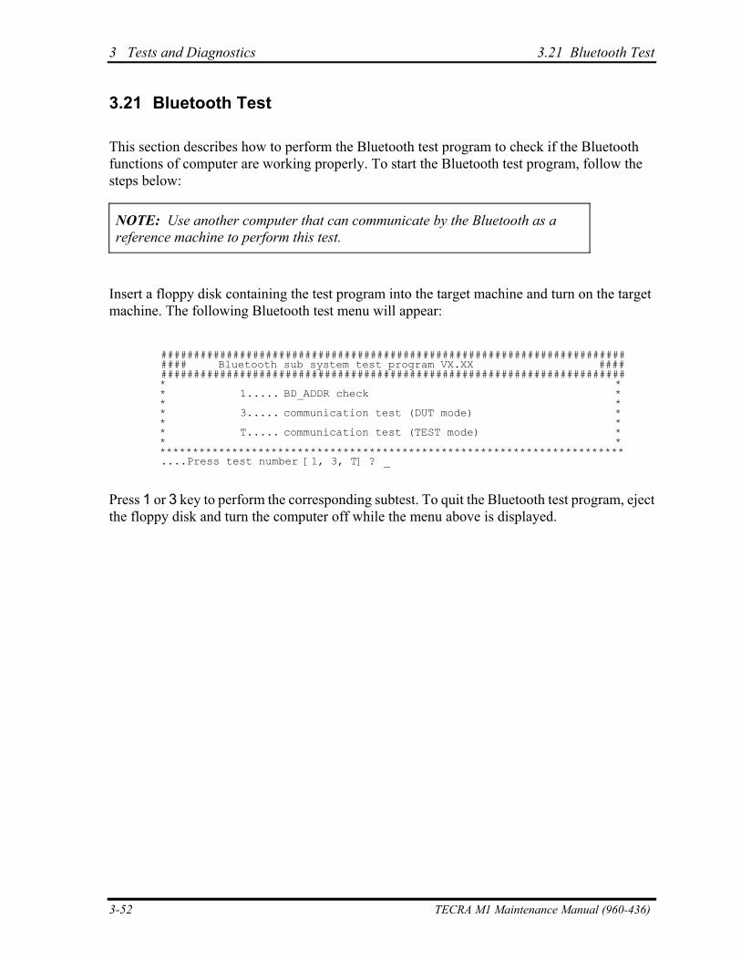
3 Tests and Diagnostics 3.21 Bluetooth Test
3.21 Bluetooth Test
This section describes how to perform the Bluetooth test program to check if the Bluetooth functions of computer are working properly. To start the Bluetooth test program, follow the steps below:
NOTE: Use another computer that can communicate by the Bluetooth as a reference machine to perform this test.
Insert a floppy disk containing the test program into the target machine and turn on the target machine. The following Bluetooth test menu will appear:
####################################################################### #### Bluetooth sub system test program VX.XX #### ####################################################################### * * * 1..... BD_ADDR check * * * * 3..... communication test (DUT mode) * * * * T..... communication test (TEST mode) * * * *********************************************************************** ....Press test number [1, 3, T] ? _
Press 1 or 3 key to perform the corresponding subtest. To quit the Bluetooth test program, eject the floppy disk and turn the computer off while the menu above is displayed.
3-52 TECRA M1 Maintenance Manual (960-436)
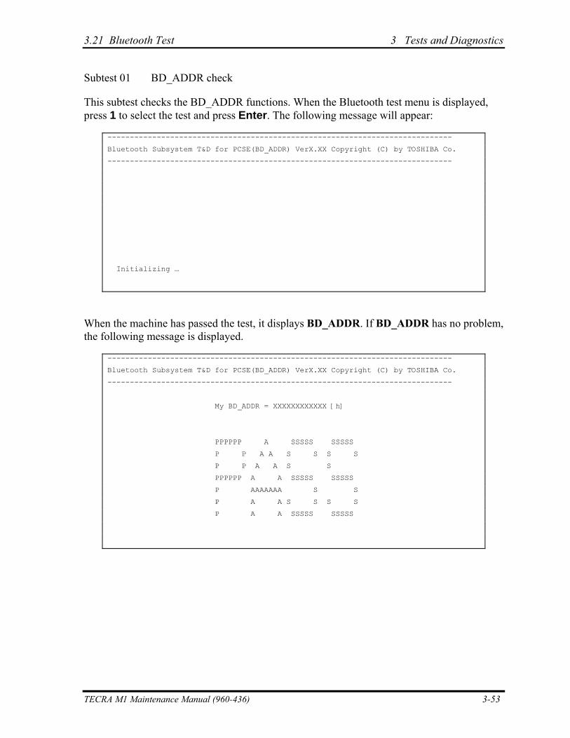
3.21 Bluetooth Test 3 Tests and Diagnostics
Subtest 01 BD_ADDR check
This subtest checks the BD_ADDR functions. When the Bluetooth test menu is displayed, press 1 to select the test and press Enter. The following message will appear:
-----------------------------------------------------------------------------
Bluetooth Subsystem T&D for PCSE(BD_ADDR) VerX.XX Copyright (C) by TOSHIBA Co.
-----------------------------------------------------------------------------
Initializing …
When the machine has passed the test, it displays BD_ADDR. If BD_ADDR has no problem, the following message is displayed.
-----------------------------------------------------------------------------
Bluetooth Subsystem T&D for PCSE(BD_ADDR) VerX.XX Copyright (C) by TOSHIBA Co.
-----------------------------------------------------------------------------
My BD_ADDR = XXXXXXXXXXXX [h]
PPPPPP A SSSSS SSSSS
P P A A S S S S
P P A A S S
PPPPPP A A SSSSS SSSSS
P AAAAAAA S S
P A A S S S S
P A A SSSSS SSSSS
TECRA M1 Maintenance Manual (960-436) 3-53
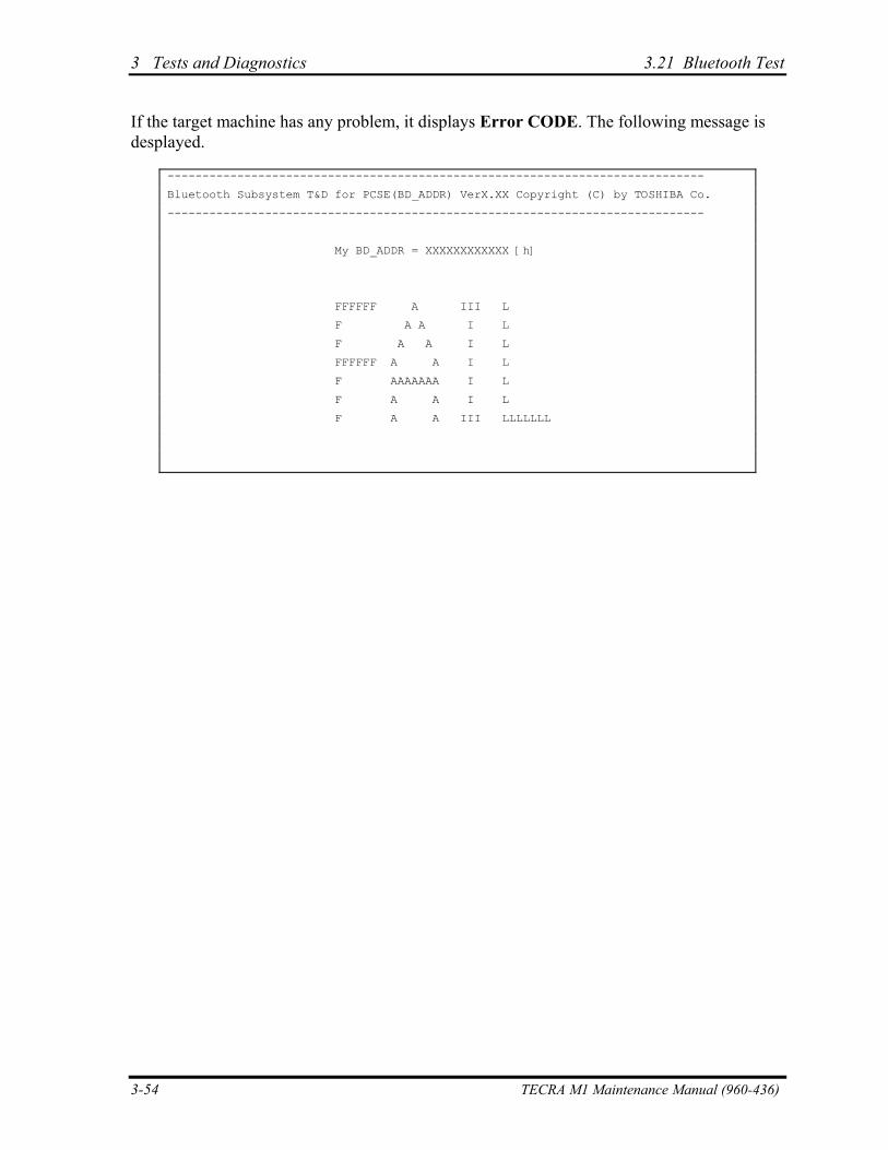
3 Tests and Diagnostics 3.21 Bluetooth Test
If the target machine has any problem, it displays Error CODE. The following message is desplayed.
-----------------------------------------------------------------------------
Bluetooth Subsystem T&D for PCSE(BD_ADDR) VerX.XX Copyright (C) by TOSHIBA Co.
-----------------------------------------------------------------------------
My BD_ADDR = XXXXXXXXXXXX [h]
FFFFFF A III L
F A A I L
F A A I L
FFFFFF A A I L
F AAAAAAA I L
F A A I L
F A A III LLLLLLL
3-54 TECRA M1 Maintenance Manual (960-436)
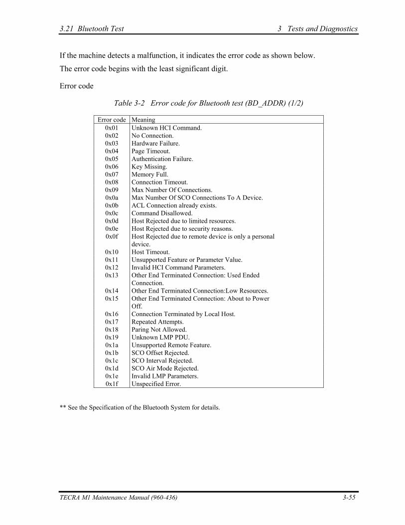
3.21 Bluetooth Test 3 Tests and Diagnostics
If the machine detects a malfunction, it indicates the error code as shown below.
The error code begins with the least significant digit.
Error code
Table 3-2 Error code for Bluetooth test (BD_ADDR) (1/2)
Error code Meaning 0x01 Unknown HCI Command. 0x02 No Connection. 0x03 Hardware Failure. 0x04 Page Timeout. 0x05 Authentication Failure. 0x06 Key Missing. 0x07 Memory Full. 0x08 Connection Timeout. 0x09 Max Number Of Connections. 0x0a Max Number Of SCO Connections To A Device. 0x0b ACL Connection already exists. 0x0c Command Disallowed. 0x0d Host Rejected due to limited resources. 0x0e Host Rejected due to security reasons. 0x0f Host Rejected due to remote device is only a personal
device. 0x10 Host Timeout. 0x11 Unsupported Feature or Parameter Value. 0x12 Invalid HCI Command Parameters. 0x13 Other End Terminated Connection: Used Ended
Connection. 0x14 Other End Terminated Connection:Low Resources. 0x15 Other End Terminated Connection: About to Power
Off. 0x16 Connection Terminated by Local Host. 0x17 Repeated Attempts. 0x18 Paring Not Allowed. 0x19 Unknown LMP PDU. 0x1a Unsupported Remote Feature. 0x1b SCO Offset Rejected. 0x1c SCO Interval Rejected. 0x1d SCO Air Mode Rejected. 0x1e Invalid LMP Parameters. 0x1f Unspecified Error.
** See the Specification of the Bluetooth System for details.
TECRA M1 Maintenance Manual (960-436) 3-55
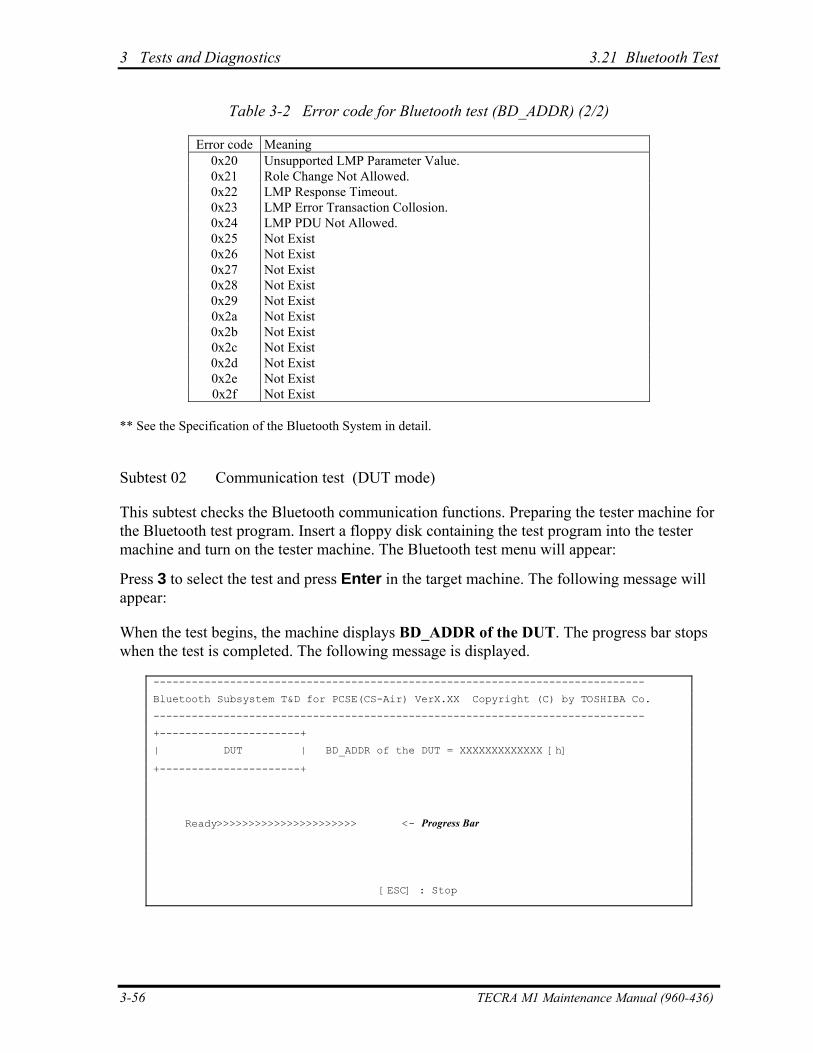
3 Tests and Diagnostics 3.21 Bluetooth Test
Table 3-2 Error code for Bluetooth test (BD_ADDR) (2/2)
Error code Meaning 0x20 Unsupported LMP Parameter Value. 0x21 Role Change Not Allowed. 0x22 LMP Response Timeout. 0x23 LMP Error Transaction Collosion. 0x24 LMP PDU Not Allowed. 0x25 Not Exist 0x26 Not Exist 0x27 Not Exist 0x28 Not Exist 0x29 Not Exist 0x2a Not Exist 0x2b Not Exist 0x2c Not Exist 0x2d Not Exist 0x2e Not Exist 0x2f Not Exist
** See the Specification of the Bluetooth System in detail.
Subtest 02 Communication test (DUT mode)
This subtest checks the Bluetooth communication functions. Preparing the tester machine for the Bluetooth test program. Insert a floppy disk containing the test program into the tester machine and turn on the tester machine. The Bluetooth test menu will appear:
Press 3 to select the test and press Enter in the target machine. The following message will appear:
When the test begins, the machine displays BD_ADDR of the DUT. The progress bar stops when the test is completed. The following message is displayed.
-----------------------------------------------------------------------------
Bluetooth Subsystem T&D for PCSE(CS-Air) VerX.XX Copyright (C) by TOSHIBA Co.
-----------------------------------------------------------------------------
+----------------------+
| DUT | BD_ADDR of the DUT = XXXXXXXXXXXXX [h]
+----------------------+
Ready>>>>>>>>>>>>>>>>>>>>>> <- Progress Bar
[ESC] : Stop
3-56 TECRA M1 Maintenance Manual (960-436)
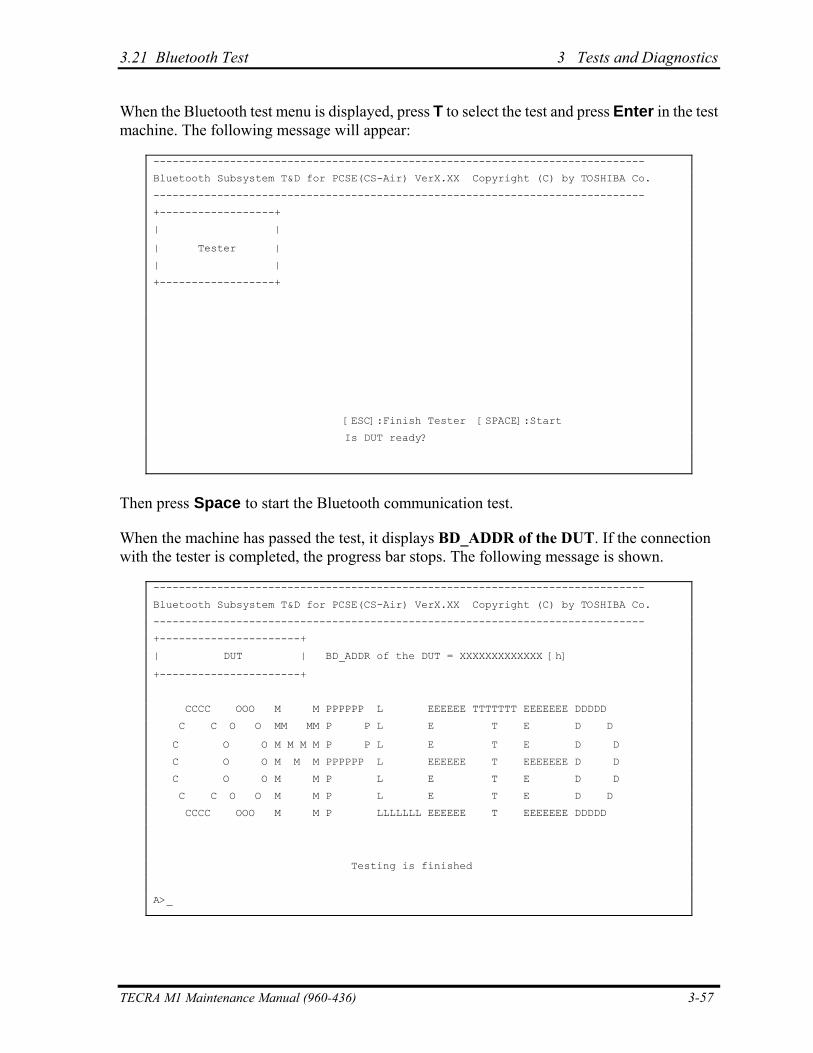
3.21 Bluetooth Test 3 Tests and Diagnostics
When the Bluetooth test menu is displayed, press T to select the test and press Enter in the test machine. The following message will appear:
-----------------------------------------------------------------------------
Bluetooth Subsystem T&D for PCSE(CS-Air) VerX.XX Copyright (C) by TOSHIBA Co.
-----------------------------------------------------------------------------
+------------------+
| |
| Tester |
| |
+------------------+
[ESC]:Finish Tester [SPACE]:Start
Is DUT ready?
Then press Space to start the Bluetooth communication test.
When the machine has passed the test, it displays BD_ADDR of the DUT. If the connection with the tester is completed, the progress bar stops. The following message is shown.
-----------------------------------------------------------------------------
Bluetooth Subsystem T&D for PCSE(CS-Air) VerX.XX Copyright (C) by TOSHIBA Co.
-----------------------------------------------------------------------------
+----------------------+
| DUT | BD_ADDR of the DUT = XXXXXXXXXXXXX [h]
+----------------------+
CCCC OOO M M PPPPPP L EEEEEE TTTTTTT EEEEEEE DDDDD
C C O O MM MM P P L E T E D D
C O O M M M M P P L E T E D D
C O O M M M PPPPPP L EEEEEE T EEEEEEE D D
C O O M M P L E T E D D
C C O O M M P L E T E D D
CCCC OOO M M P LLLLLLL EEEEEE T EEEEEEE DDDDD
Testing is finished
A>_
TECRA M1 Maintenance Manual (960-436) 3-57
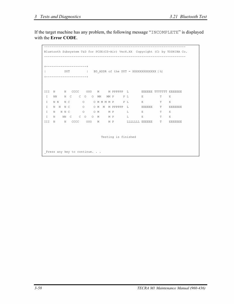
3 Tests and Diagnostics 3.21 Bluetooth Test
If the target machine has any problem, the following message “INCOMPLETE” is displayed with the Error CODE.
-----------------------------------------------------------------------------
Bluetooth Subsystem T&D for PCSE(CS-Air) VerX.XX Copyright (C) by TOSHIBA Co.
-----------------------------------------------------------------------------
+----------------------+
| DUT | BD_ADDR of the DUT = XXXXXXXXXXXXX [h]
+----------------------+
III N N CCCC OOO M M PPPPPP L EEEEEE TTTTTTT EEEEEEE
I NN N C C O O MM MM P P L E T E
I N N N C O O M M M M P P L E T E
I N N N C O O M M M PPPPPP L EEEEEE T EEEEEEE
I N N N C O O M M P L E T E
I N NN C C O O M M P L E T E
III N N CCCC OOO M M P LLLLLLL EEEEEE T EEEEEEE
Testing is finished
_Press any key to continue. . .
3-58 TECRA M1 Maintenance Manual (960-436)
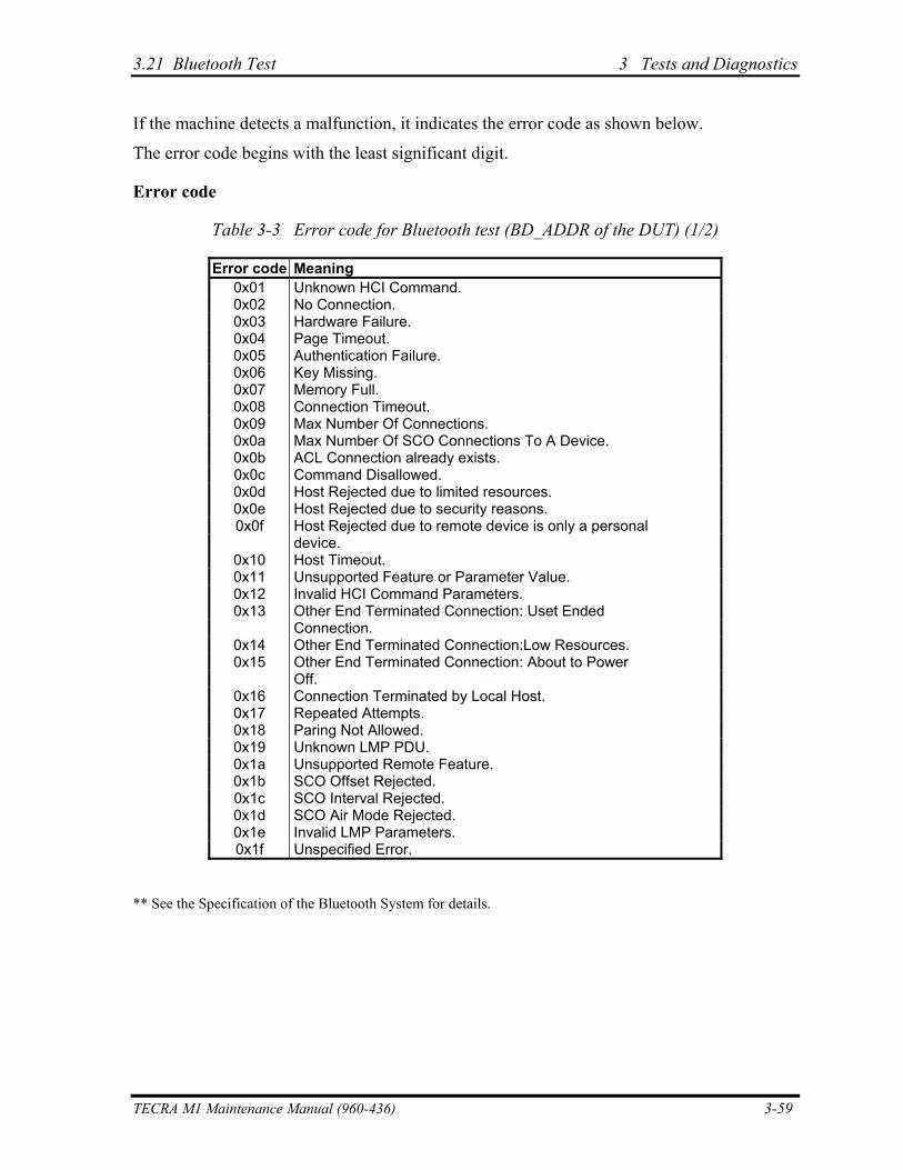
3.21 Bluetooth Test 3 Tests and Diagnostics
If the machine detects a malfunction, it indicates the error code as shown below.
The error code begins with the least significant digit.
Error code
Table 3-3 Error code for Bluetooth test (BD_ADDR of the DUT) (1/2)
Error code Meaning 0x01 Unknown HCI Command. 0x02 No Connection. 0x03 Hardware Failure. 0x04 Page Timeout. 0x05 Authentication Failure. 0x06 Key Missing. 0x07 Memory Full. 0x08 Connection Timeout. 0x09 Max Number Of Connections. 0x0a Max Number Of SCO Connections To A Device. 0x0b ACL Connection already exists. 0x0c Command Disallowed. 0x0d Host Rejected due to limited resources. 0x0e Host Rejected due to security reasons. 0x0f Host Rejected due to remote device is only a personal
device. 0x10 Host Timeout. 0x11 Unsupported Feature or Parameter Value. 0x12 Invalid HCI Command Parameters. 0x13 Other End Terminated Connection: Uset Ended
Connection. 0x14 Other End Terminated Connection:Low Resources. 0x15 Other End Terminated Connection: About to Power
Off. 0x16 Connection Terminated by Local Host. 0x17 Repeated Attempts. 0x18 Paring Not Allowed. 0x19 Unknown LMP PDU. 0x1a Unsupported Remote Feature. 0x1b SCO Offset Rejected. 0x1c SCO Interval Rejected. 0x1d SCO Air Mode Rejected. 0x1e Invalid LMP Parameters. 0x1f Unspecified Error.
** See the Specification of the Bluetooth System for details.
TECRA M1 Maintenance Manual (960-436) 3-59
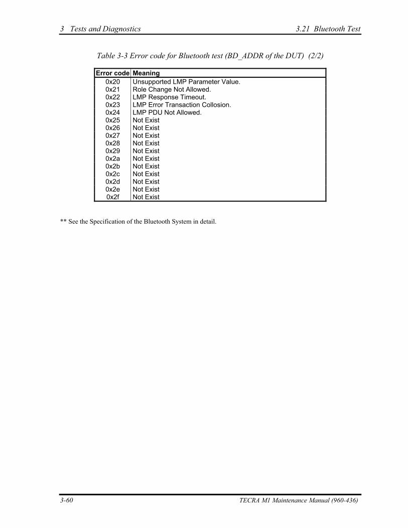
3 Tests and Diagnostics 3.21 Bluetooth Test
Table 3-3 Error code for Bluetooth test (BD_ADDR of the DUT) (2/2)
Error code Meaning 0x20 Unsupported LMP Parameter Value. 0x21 Role Change Not Allowed. 0x22 LMP Response Timeout. 0x23 LMP Error Transaction Collosion. 0x24 LMP PDU Not Allowed. 0x25 Not Exist 0x26 Not Exist 0x27 Not Exist 0x28 Not Exist 0x29 Not Exist 0x2a Not Exist 0x2b Not Exist 0x2c Not Exist 0x2d Not Exist 0x2e Not Exist 0x2f Not Exist
** See the Specification of the Bluetooth System in detail.
3-60 TECRA M1 Maintenance Manual (960-436)
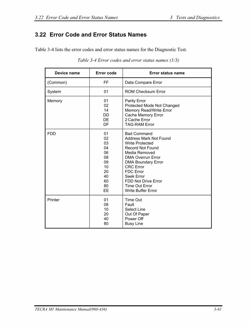
3.22 Error Code and Error Status Names 3 Tests and Diagnostics
3.22 Error Code and Error Status Names
Table 3-4 lists the error codes and error status names for the Diagnostic Test.
Table 3-4 Error codes and error status names (1/3)
Device name Error code Error status name
(Common) FF Data Compare Error
System 01 ROM Checksum Error
Memory 01 02 14 DD DE DF
Parity Error Protected Mode Not Changed Memory Read/Write Error Cache Memory Error 2 Cache Error TAG-RAM Error
FDD 01 02 03 04 06 08 09 10 20 40 60 80 EE
Bad Command Address Mark Not Found Write Protected Record Not Found Media Removed DMA Overrun Error DMA Boundary Error CRC Error FDC Error Seek Error FDD Not Drive Error Time Out Error Write Buffer Error
Printer 01 08 10 20 40 80
Time Out Fault Select Line Out Of Paper Power Off Busy Line
TECRA M1 Maintenance Manual(960-436) 3-61
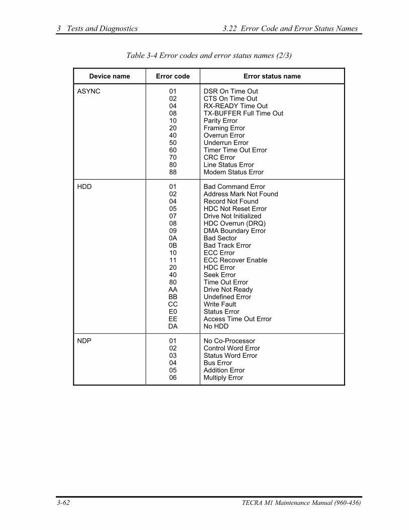
3 Tests and Diagnostics 3.22 Error Code and Error Status Names
Table 3-4 Error codes and error status names (2/3)
Device name Error code Error status name
ASYNC 01 02 04 08 10 20 40 50 60 70 80 88
DSR On Time Out CTS On Time Out RX-READY Time Out TX-BUFFER Full Time Out Parity Error Framing Error Overrun Error Underrun Error Timer Time Out Error CRC Error Line Status Error Modem Status Error
HDD 01 02 04 05 07 08 09 0A 0B 10 11 20 40 80 AA BB CC E0 EE DA
Bad Command Error Address Mark Not Found Record Not Found HDC Not Reset Error Drive Not Initialized HDC Overrun (DRQ) DMA Boundary Error Bad Sector Bad Track Error ECC Error ECC Recover Enable HDC Error Seek Error Time Out Error Drive Not Ready Undefined Error Write Fault Status Error Access Time Out Error No HDD
NDP 01 02 03 04 05 06
No Co-Processor Control Word Error Status Word Error Bus Error Addition Error Multiply Error
3-62 TECRA M1 Maintenance Manual (960-436)
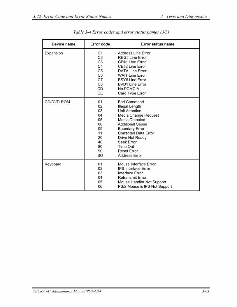
3.22 Error Code and Error Status Names 3 Tests and Diagnostics
Table 3-4 Error codes and error status names (3/3)
Device name Error code Error status name
Expansion C1 C2 C3 C4 C5 C6 C7 C8 CD CE
Address Line Error REG# Line Error CE#1 Line Error CE#2 Line Error DATA Line Error WAIT Line Error BSY# Line Error BVD1 Line Error No PCMCIA Card Type Error
CD/DVD-ROM 01 02 03 04 05 06 09 11 20 40 80 90 BO
Bad Command Illegal Length Unit Attention Media Change Request Media Detected Additional Sense Boundary Error Corrected Data Error Drive Not Ready Seek Error Time Out Reset Error Address Error
Keyboard 01 02 03 04 05 06
Mouse Interface Error IPS Interface Error Interface Error Retransmit Error Mouse Handler Not Support PS/2 Mouse & IPS Not Support
TECRA M1 Maintenance Manual(960-436) 3-63
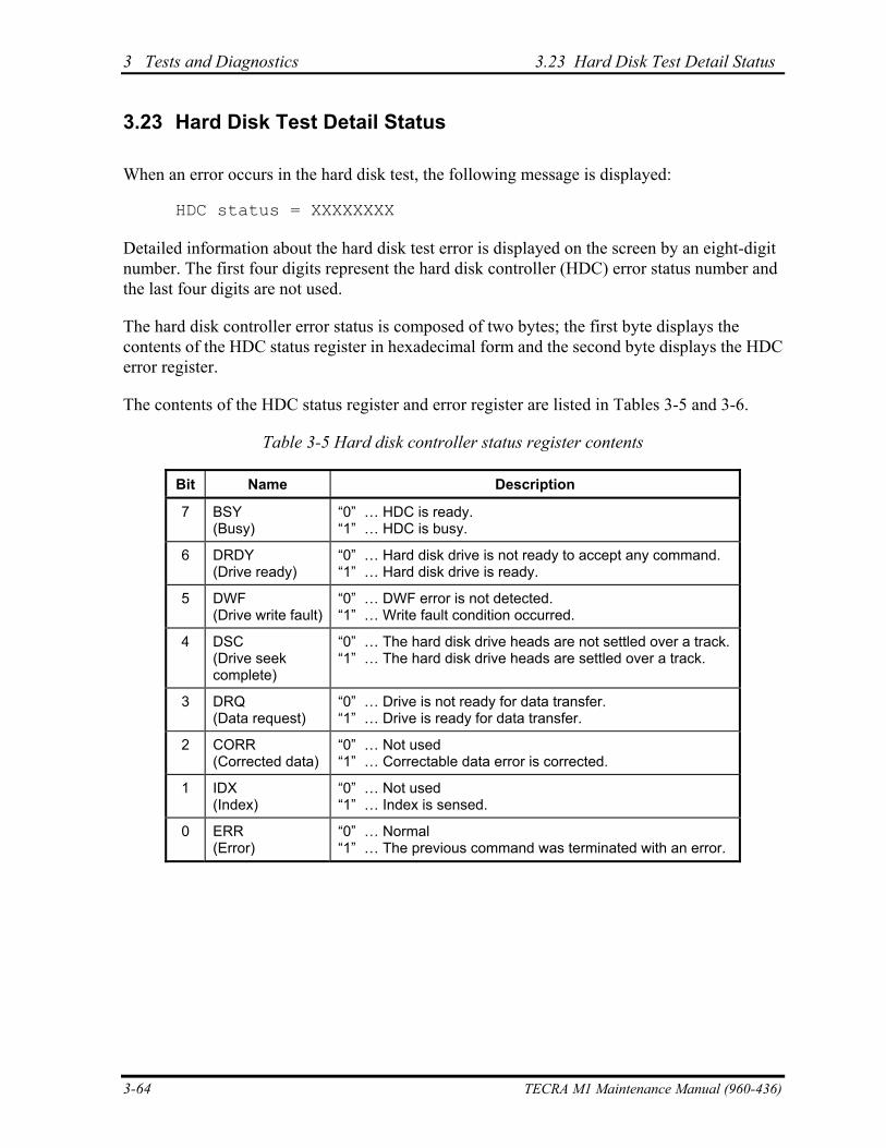
3 Tests and Diagnostics 3.23 Hard Disk Test Detail Status
3.23 Hard Disk Test Detail Status
When an error occurs in the hard disk test, the following message is displayed:
HDC status = XXXXXXXX
Detailed information about the hard disk test error is displayed on the screen by an eight-digit number. The first four digits represent the hard disk controller (HDC) error status number and the last four digits are not used.
The hard disk controller error status is composed of two bytes; the first byte displays the contents of the HDC status register in hexadecimal form and the second byte displays the HDC error register.
The contents of the HDC status register and error register are listed in Tables 3-5 and 3-6.
Table 3-5 Hard disk controller status register contents
Bit Name Description
7 BSY (Busy)
“0” … HDC is ready. “1” … HDC is busy.
6 DRDY (Drive ready)
“0” … Hard disk drive is not ready to accept any command. “1” … Hard disk drive is ready.
5 DWF (Drive write fault)
“0” … DWF error is not detected. “1” … Write fault condition occurred.
4 DSC (Drive seek complete)
“0” … The hard disk drive heads are not settled over a track.“1” … The hard disk drive heads are settled over a track.
3 DRQ (Data request)
“0” … Drive is not ready for data transfer. “1” … Drive is ready for data transfer.
2 CORR (Corrected data)
“0” … Not used “1” … Correctable data error is corrected.
1 IDX (Index)
“0” … Not used “1” … Index is sensed.
0 ERR (Error)
“0” … Normal “1” … The previous command was terminated with an error.
3-64 TECRA M1 Maintenance Manual (960-436)
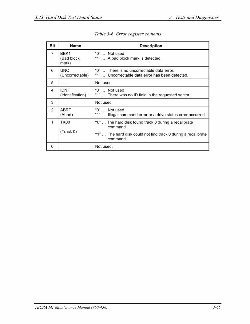
3.23 Hard Disk Test Detail Status 3 Tests and Diagnostics
Table 3-6 Error register contents
Bit Name Description
7 BBK1 (Bad block mark)
“0” … Not used “1” … A bad block mark is detected.
6 UNC (Uncorrectable)
“0” … There is no uncorrectable data error. “1” … Uncorrectable data error has been detected.
5 —— Not used
4 IDNF (Identification)
“0” … Not used “1” … There was no ID field in the requested sector.
3 —— Not used
2 ABRT (Abort)
“0” … Not used “1” … Illegal command error or a drive status error occurred.
1 TK00 (Track 0)
“0” … The hard disk found track 0 during a recalibrate command.
“1” … The hard disk could not find track 0 during a recalibrate command.
0 —— Not used.
TECRA M1 Maintenance Manual (960-436) 3-65
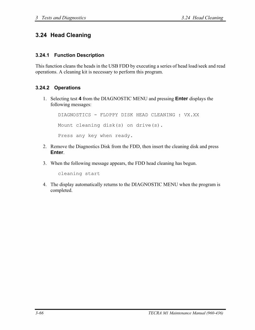
3 Tests and Diagnostics 3.24 Head Cleaning
3.24 Head Cleaning
3.24.1 Function Description
This function cleans the heads in the USB FDD by executing a series of head load/seek and read operations. A cleaning kit is necessary to perform this program.
3.24.2 Operations
1. Selecting test 4 from the DIAGNOSTIC MENU and pressing Enter displays the following messages:
DIAGNOSTICS - FLOPPY DISK HEAD CLEANING : VX.XX
Mount cleaning disk(s) on drive(s).
Press any key when ready.
2. Remove the Diagnostics Disk from the FDD, then insert the cleaning disk and press Enter.
3. When the following message appears, the FDD head cleaning has begun.
cleaning start
4. The display automatically returns to the DIAGNOSTIC MENU when the program is completed.
3-66 TECRA M1 Maintenance Manual (960-436)
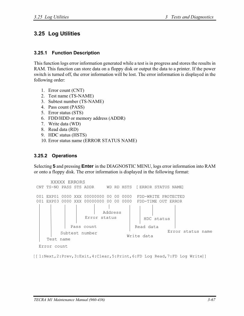
3.25 Log Utilities 3 Tests and Diagnostics
3.25 Log Utilities
3.25.1 Function Description
This function logs error information generated while a test is in progress and stores the results in RAM. This function can store data on a floppy disk or output the data to a printer. If the power switch is turned off, the error information will be lost. The error information is displayed in the following order:
1. Error count (CNT) 2. Test name (TS-NAME) 3. Subtest number (TS-NAME) 4. Pass count (PASS) 5. Error status (STS) 6. FDD/HDD or memory address (ADDR) 7. Write data (WD) 8. Read data (RD) 9. HDC status (HSTS) 10. Error status name (ERROR STATUS NAME)
3.25.2 Operations
Selecting 5 and pressing Enter in the DIAGNOSTIC MENU, logs error information into RAM or onto a floppy disk. The error information is displayed in the following format:
[[1:Next,2:Prev,3:Exit,4:Clear,5:Print,6:FD Log Read,7:FD Log Write]]
XXXXX ERRORSCNT TS-NO PASS STS ADDR WD RD HSTS [ERROR STATUS NAME]
001 EXP01 0000 XXX 00000000 00 00 0000 FDD-WRITE PROTECTED001 EXP03 0000 XXX 00000000 00 00 0000 FDD-TIME OUT ERROR
Error status name
Error count
Pass count
Error status
Subtest number
Address
Test name
Read data
Write data
HDC status
TECRA M1 Maintenance Manual (960-436) 3-67
3 Tests and Diagnostics 3.25 Log Utilities
2. The error information displayed on the screen can be manipulated by the following number keys:
1 scrolls the display to the next page. 2 scrolls the display to the previous page. 3 returns to the Diagnostic Menu. 4 erases all error log information in RAM. 5 outputs the error log information to a printer. 6 reads the log information from a floppy disk. 7 writes the log information to a floppy disk.
3. In the case of “error retry OK”, a capital “R” will be placed at the beginning of the error status. However, it is not added to the error count.
3-68 TECRA M1 Maintenance Manual (960-436)
3.26 Running Test 3 Tests and Diagnostics
3.26 Running Test
3.26.1 Function Description
This function automatically executes the following tests in sequence:
1. System test (subtest 01) 2. Memory test (subtests 01, 02, 04, and 06) 3. Real timer test (subtest 02) 4. Display test (subtest 01) 5. FDD test (subtest 02) 6. HDD test (subtests 01 and 05) 7. Printer test (subtest 03) if selected 8. Async test (subtest 01) (not supported in this model)
3.26.2 Operations
NOTE: Do not forget to load a work disk in the FDD. If a work disk is not loaded, an error will be generated during the FDD testing.
1. Remove the diagnostics disk from the floppy disk drive and insert the work disk.
2. Select 6 from the Diagnostic Menu and press Enter, the following message displays:
Printer wrap around test (Y/N) ?
Selecting Y (yes) executes the printer wraparound test. A printer wraparound connector must be connected to the parallel port of the computer to properly execute this test.
3. Select Y or N and press Enter. The following message will appear:
Serial#A wrap around test (Y/N) ?
Selecting Y (yes) executes the ASYNC wraparound test. An RS-232-C wraparound connector must be connected to the serial port of the computer to properly execute this test.
TECRA M1 Maintenance Manual (960-436) 3-69
3 Tests and Diagnostics 3.26 Running Test
4. Select No and press Enter. The following message will appear:
Mount the work disk(s) on the drive(s), then press [Enter] key. [Warning : The contents of the disk(s), will be destroyed.]
5. This program is executed continuously. To terminate the program, press Ctrl +Break.
3-70 TECRA M1 Maintenance Manual (960-436)
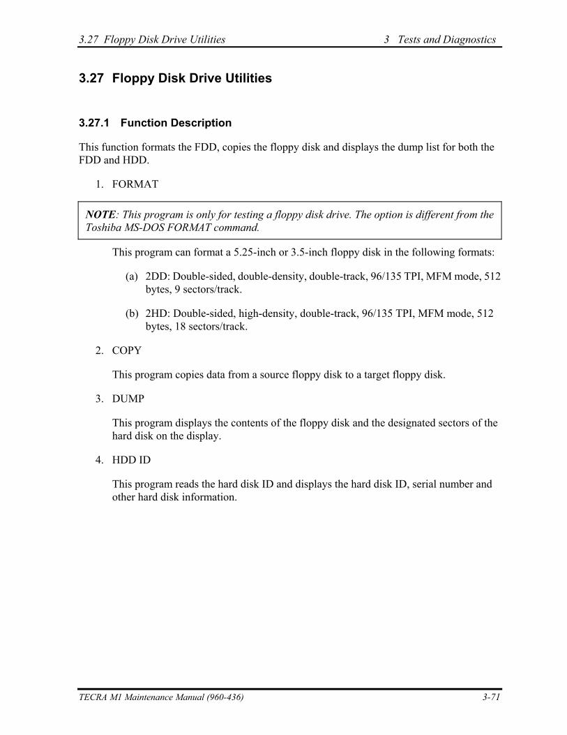
3.27 Floppy Disk Drive Utilities 3 Tests and Diagnostics
3.27 Floppy Disk Drive Utilities
3.27.1 Function Description
This function formats the FDD, copies the floppy disk and displays the dump list for both the FDD and HDD.
1. FORMAT
NOTE: This program is only for testing a floppy disk drive. The option is different from the Toshiba MS-DOS FORMAT command.
This program can format a 5.25-inch or 3.5-inch floppy disk in the following formats:
(a) 2DD: Double-sided, double-density, double-track, 96/135 TPI, MFM mode, 512 bytes, 9 sectors/track.
(b) 2HD: Double-sided, high-density, double-track, 96/135 TPI, MFM mode, 512 bytes, 18 sectors/track.
2. COPY
This program copies data from a source floppy disk to a target floppy disk.
3. DUMP
This program displays the contents of the floppy disk and the designated sectors of the hard disk on the display.
4. HDD ID
This program reads the hard disk ID and displays the hard disk ID, serial number and other hard disk information.
TECRA M1 Maintenance Manual (960-436) 3-71
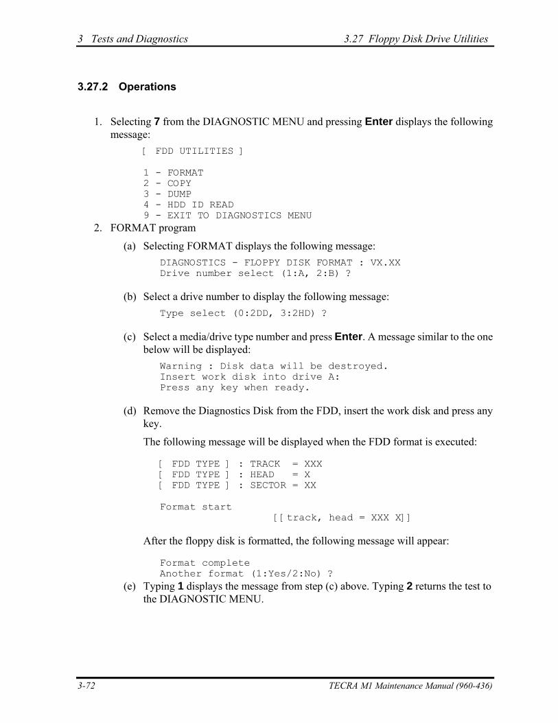
3 Tests and Diagnostics 3.27 Floppy Disk Drive Utilities
3.27.2 Operations
1. Selecting 7 from the DIAGNOSTIC MENU and pressing Enter displays the following message:
[ FDD UTILITIES ]
1 - FORMAT 2 - COPY 3 - DUMP 4 - HDD ID READ 9 - EXIT TO DIAGNOSTICS MENU
2. FORMAT program
(a) Selecting FORMAT displays the following message: DIAGNOSTICS - FLOPPY DISK FORMAT : VX.XX Drive number select (1:A, 2:B) ?
(b) Select a drive number to display the following message: Type select (0:2DD, 3:2HD) ?
(c) Select a media/drive type number and press Enter. A message similar to the one below will be displayed:
Warning : Disk data will be destroyed. Insert work disk into drive A: Press any key when ready.
(d) Remove the Diagnostics Disk from the FDD, insert the work disk and press any key.
The following message will be displayed when the FDD format is executed:
[ FDD TYPE ] : TRACK = XXX [ FDD TYPE ] : HEAD = X [ FDD TYPE ] : SECTOR = XX
Format start [[track, head = XXX X]]
After the floppy disk is formatted, the following message will appear:
Format complete Another format (1:Yes/2:No) ?
(e) Typing 1 displays the message from step (c) above. Typing 2 returns the test to the DIAGNOSTIC MENU.
3-72 TECRA M1 Maintenance Manual (960-436)
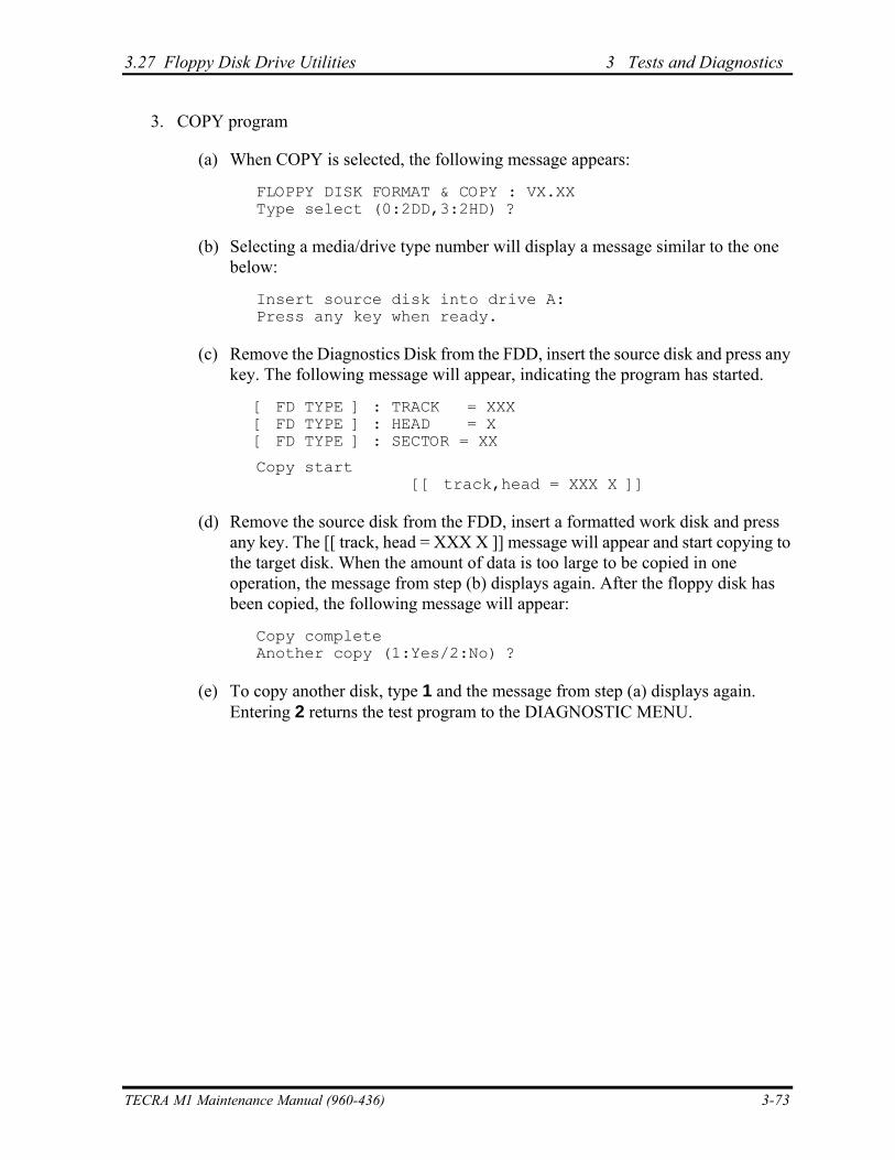
3.27 Floppy Disk Drive Utilities 3 Tests and Diagnostics
3. COPY program
(a) When COPY is selected, the following message appears:
FLOPPY DISK FORMAT & COPY : VX.XX Type select (0:2DD,3:2HD) ?
(b) Selecting a media/drive type number will display a message similar to the one below:
Insert source disk into drive A: Press any key when ready.
(c) Remove the Diagnostics Disk from the FDD, insert the source disk and press any key. The following message will appear, indicating the program has started.
[ FD TYPE ] : TRACK = XXX [ FD TYPE ] : HEAD = X [ FD TYPE ] : SECTOR = XX
Copy start [[ track,head = XXX X ]]
(d) Remove the source disk from the FDD, insert a formatted work disk and press any key. The [[ track, head = XXX X ]] message will appear and start copying to the target disk. When the amount of data is too large to be copied in one operation, the message from step (b) displays again. After the floppy disk has been copied, the following message will appear:
Copy complete Another copy (1:Yes/2:No) ?
(e) To copy another disk, type 1 and the message from step (a) displays again. Entering 2 returns the test program to the DIAGNOSTIC MENU.
TECRA M1 Maintenance Manual (960-436) 3-73
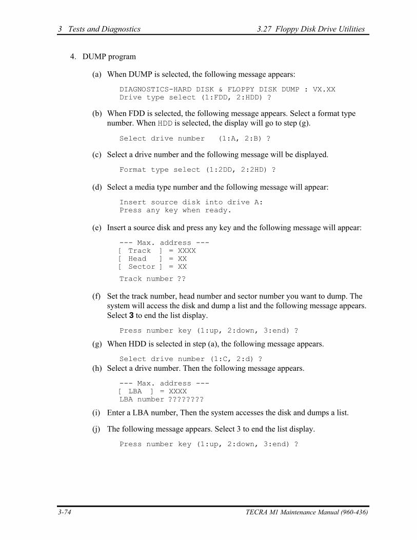
3 Tests and Diagnostics 3.27 Floppy Disk Drive Utilities
4. DUMP program
(a) When DUMP is selected, the following message appears:
DIAGNOSTICS-HARD DISK & FLOPPY DISK DUMP : VX.XX Drive type select (1:FDD, 2:HDD) ?
(b) When FDD is selected, the following message appears. Select a format type number. When HDD is selected, the display will go to step (g).
Select drive number (1:A, 2:B) ?
(c) Select a drive number and the following message will be displayed.
Format type select (1:2DD, 2:2HD) ?
(d) Select a media type number and the following message will appear:
Insert source disk into drive A: Press any key when ready.
(e) Insert a source disk and press any key and the following message will appear:
--- Max. address --- [ Track ] = XXXX [ Head ] = XX [ Sector ] = XX
Track number ??
(f) Set the track number, head number and sector number you want to dump. The system will access the disk and dump a list and the following message appears. Select 3 to end the list display.
Press number key (1:up, 2:down, 3:end) ?
(g) When HDD is selected in step (a), the following message appears.
Select drive number (1:C, 2:d) ? (h) Select a drive number. Then the following message appears.
--- Max. address --- [ LBA ] = XXXX LBA number ????????
(i) Enter a LBA number, Then the system accesses the disk and dumps a list.
(j) The following message appears. Select 3 to end the list display.
Press number key (1:up, 2:down, 3:end) ?
3-74 TECRA M1 Maintenance Manual (960-436)
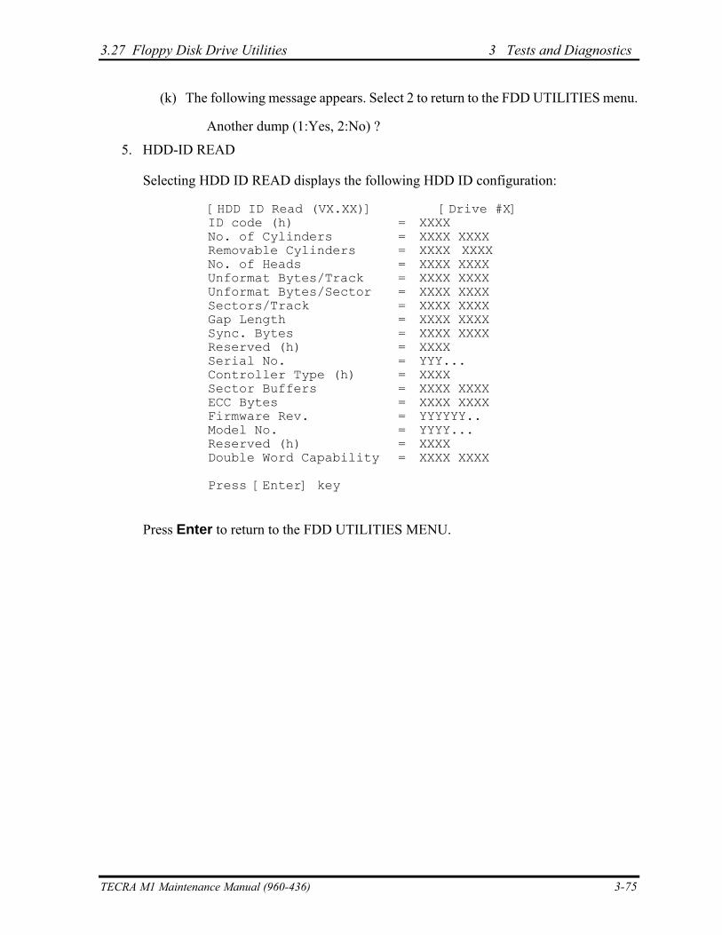
3.27 Floppy Disk Drive Utilities 3 Tests and Diagnostics
TECRA M1 Maintenance Manual (960-436) 3-75
(k) The following message appears. Select 2 to return to the FDD UTILITIES menu.
Another dump (1:Yes, 2:No) ?
5. HDD-ID READ
Selecting HDD ID READ displays the following HDD ID configuration:
[HDD ID Read (VX.XX)] [Drive #X] ID code (h) = XXXX No. of Cylinders = XXXX XXXX Removable Cylinders = XXXX XXXX No. of Heads = XXXX XXXX Unformat Bytes/Track = XXXX XXXX Unformat Bytes/Sector = XXXX XXXX Sectors/Track = XXXX XXXX Gap Length = XXXX XXXX Sync. Bytes = XXXX XXXX Reserved (h) = XXXX Serial No. = YYY... Controller Type (h) = XXXX Sector Buffers = XXXX XXXX ECC Bytes = XXXX XXXX Firmware Rev. = YYYYYY.. Model No. = YYYY... Reserved (h) = XXXX Double Word Capability = XXXX XXXX Press [Enter] key
Press Enter to return to the FDD UTILITIES MENU.
3 Tests and Diagnostics 3.28 System Configuration
3
3.28 System Configuration
3.28.1 Function Description
The System Configuration program contains the following configuration information for the computer:
1. Processor Type
2. VGA Controller
3. MS-DOS Version
4. BIOS ROM version (1st ID, 2nd ID)
5. Boot ROM version
6. KBC version
7. PS Microprocessor Version
8. Total Memory Size
9. Battery code
10. Sound System
11. The number of printer ports
12. The number of ASYNC ports
13. The number of math co-processors
14. The number of PCMCIA Slots
15. Modem Type
16. LAN Type
17. The number of floppy disk drives
18. The number of hard disk drives
19. Date/Time
3-76 TECRA M1 Maintenance Manual (960-436)
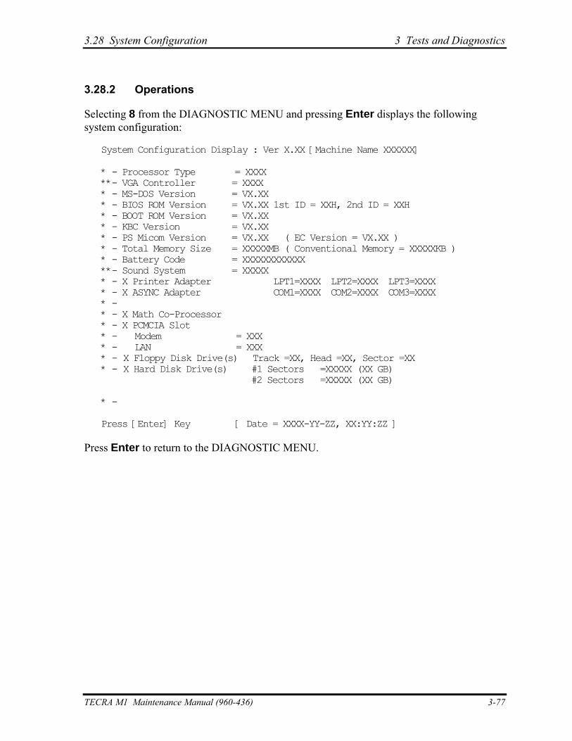
3.28 System Configuration 3 Tests and Diagnostics
3.28.2 Operations
Selecting 8 from the DIAGNOSTIC MENU and pressing Enter displays the following system configuration:
System Configuration Display : Ver X.XX [Machine Name XXXXXX]
* - Processor Type = XXXX **- VGA Controller = XXXX * - MS-DOS Version = VX.XX * - BIOS ROM Version = VX.XX 1st ID = XXH, 2nd ID = XXH * - BOOT ROM Version = VX.XX * - KBC Version = VX.XX * - PS Micom Version = VX.XX ( EC Version = VX.XX ) * - Total Memory Size = XXXXXMB ( Conventional Memory = XXXXXKB ) * - Battery Code = XXXXXXXXXXXX **- Sound System = XXXXX * - X Printer Adapter LPT1=XXXX LPT2=XXXX LPT3=XXXX * - X ASYNC Adapter COM1=XXXX COM2=XXXX COM3=XXXX * - * - X Math Co-Processor * - X PCMCIA Slot * - Modem = XXX * - LAN = XXX * - X Floppy Disk Drive(s) Track =XX, Head =XX, Sector =XX * - X Hard Disk Drive(s) #1 Sectors =XXXXX (XX GB)
#2 Sectors =XXXXX (XX GB) * - Press [Enter] Key [ Date = XXXX-YY-ZZ, XX:YY:ZZ ]
Press Enter to return to the DIAGNOSTIC MENU.
TECRA M1 Maintenance Manual (960-436) 3-77
3 Tests and Diagnostics 3.29 SETUP
3.29 SETUP
3.29.1 Function Description
This program displays the current system setup information as listed below:
1. Memory (a) Total
2. System Date/Time
(a) Date (MM-DD-YYYY) (b) Time (HH:MM:SS)
3. Battery
(a) Battery Save Mode
4. Password
5. Boot Priority (a) Boot Priority (b) HDD Priority
6. Display (a) Power On Display (b) TV Type
7. Others (a) Power-up Mode (b) CPU Cache (c) Level 2 Cache (d) Dynamic CPU Frequency Mode (e) Auto Power On (f) Panel Power On/Off
8. Configuration (a) Device Config.
9. I/O Ports (a) Serial
(b) Parallel
3-78 TECRA M1 Maintenance Manual (960-436)
3.29 SETUP 3 Tests and Diagnostics
10. Drives I/O (a) Built-in HDD
(b) Select Bay
11. PCI Bus (a) PCI Bus
12. PC Card (a) Controller Mode
13. Peripheral (a) Internal Pointing Device (b) Ext keyboard “Fn” (c) Paralla Port Mode (d) Hard Disk Mode
14. Legacy Emulation (a) USB kayboard/Mouse Legacy Emulation (b) USB-FDD Legacy Emulation
15. PCI LAN (a) Built-in LAN
16. HDD Password (a) HDD
(b) HDD Password Mode
(c) User Password
TECRA M1 Maintenance Manual (960-436) 3-79
3 Tests and Diagnostics 3.29 SETUP
3.29.2 Accessing the SETUP Program
Selecting 0 from the DIAGNOSTICS MENU and pressing Enter displays the TSETUP screen. The TSETUP screen is divided into two pages: SYSTEM SETUP (1/2) and SYSTEM SETUP (2/2).
Boot Priority =HDD→FDD→CD-ROM→LANHDD Rriority
=Built-in HDD→Second HDD→PC Card
Power-up mode = BootCPU Cache = EnabledLevel 2 Cache = EnabledDynamic CPU Frequency Mode
= Dynamically SwitchableAuto Power On = DisabledPanel Power On/Off = Disabled
SYSTEM SETUP (1/2) ACPI BIOS version = X.XX
Date (MM-DD-YYYY) =XX-XX-XXXXTime (HH:MM:SS) =XX:XX:XX
Total = XXXXXXKBMEMORY
Not Registerd
BOOT PRIORITY
PASSWORD
Battery Save Mode = Full PowerBATTERY
OTHERS
SYSTEM DATE/TIME
Power On Display = Auto-Selected
TV Type = NTSC
DISPLAY
HDD = Built-in HDDHDD Password Mode = User onlyUser Password = Not Registered
HDD PASSWORD
Controller Mode = Auto-SelectedDevice Config. = Setup by OSCONFIGURATION
PCI BUS = IRQ11
Serial = COM1(3F8H/IRQ4)
Parallel = LPT1(378/IRQ7/ch3)
SYSTEM SETUP (2/2) ACPI BIOS version = X.XX
PC CARD
I/O PORTS
PCI BUS
↑↓→←: Select items Space, BkSp: Change values PgDn, PgUp: Change pagesEsc: Exit without saving Home: Set default values End: Save changes and Exit
Built-in LAN = EnabledPCI LAN
USB KB/Mouse Legacy Emulation= Enabled
USB-FDD Legacy Emulation= Enabled
LEGACY EMULATIONBuilt-in HDD
= Primary IDE(1F0H/IRG14)Select Bay
=Secondary IDE(170H/IRQ15)
DRIVES I/O
Internal Pointing Device =EnabledExt kayboard “Fn” =DisabledParallel Port Mode =ECPHard Disk Mode =Enhanced
PERIPHERAL
3-80 TECRA M1 Maintenance Manual (960-436)
3.29 SETUP 3 Tests and Diagnostics
NOTE: 1) Panel Power On/Off under OTHERS appears only when the Power-up Mode is in Resume mode. 2) USB FDD Legacy Emulation under LEGACY EMULATION appears only when Floppy Disk I/O is set to Disabled.
TECRA M1 Maintenance Manual (960-436) 3-81
3 Tests and Diagnostics 3.29 SETUP
Moving Within the SETUP Menu and Changing Values
1. Press and to move between the two columns. Press PgDn and PgUp to move between the two pages. Press ↑ and ↓ to move between items in a column.
2. Press either the space bar to change the value.
Accepting Changes and Exiting the SETUP Window
1. Press End to accept the changes you made.
The following message is displayed:
Are you sure? (Y/N) The changes you made will cause the system to reboot.
2. To make other changes, press N. Repeat the steps above.
3. To accept the changes, press Y.
NOTE: You can press Esc to quit at any time without saving changes. SETUP asks you to confirm that you do not want to save your changes toward User.
The Factory Preset Configuration
When you access SETUP, the current configuration is displayed.
1. To show the factory preset configuration, press Home.
2. Press End and then press Y to accept the factory preset settings.
NOTE: When you execute the default setting, the following settings are not changed: HDD Mode Password Write Policy in the CPU Cache
3-82 TECRA M1 Maintenance Manual (960-436)
3.29 SETUP 3 Tests and Diagnostics
SETUP Options
The SETUP screen is divided into functionally related groups. This section describes each group and its options.
1. Memory
This group of options displays the computer’s memory.
(a) Total
This field displays the total amount of memory installed and is automatically calculated by the computer. You cannot change this value.
2. System Date/Time
Use this option to set the computer’s system date/time. Press ↓ to move the cursor to the right and press ↑ to move the cursor to the left. Press the space bar to increase the number and press BkSp to decrease the number.
(a) Date
Use this option to set the system date of the computer.
(b) Time
Use this option to set the system time of the computer.
3. Battery
This option is used to select Full Power, Low Power or User Setting of the battery save mode.
(a) Battery Save Mode
When User Setting is selected, the sub-window, BATTERY SAVE OPTION is displayed. The following set of options can be selected in the submenu.
Processing Speed
This feature changes the CPU processing speed.
High CPU operates at high speed. (Default)
Low CPU operates at low speed.
CPU Sleep Mode
Use this option to enable or disable the CPU sleep function.
TECRA M1 Maintenance Manual (960-436) 3-83
3 Tests and Diagnostics 3.29 SETUP
Enabled Enables sleep mode. (Default)
Disabled Disables sleep mode.
Display Auto Off
Use this option to disable or set the duration of the display automatic power off function. This function causes the computer to turn the LCD panel’s illumination off if you make no entry for the set period of time.
Disabled Disables display automatic power off.
xx Min. Automatically turns off power to the LCD panel’s illumination if the panel is not used for the duration set. The duration xx can be set to 1, 3, 5, 10, 15, 20 or 30 minutes.
HDD Auto Off
Use this option to set the duration of the HDD automatic power off function.
xx Min. Automatically turns off power to the hard disk drive if it is not used for the duration set. The duration xx can be set to 1, 3, 5, 10, 15, 20 or 30 minutes.
LCD Brightness
Use this option to set the level of LCD brightness.
Super-Bright Full brightness for maximum visibility.
Bright Full brightness for high visibility.
Semi-Bright Less than full brightness for saving power.
Cooling Method
If the CPU becomes too hot, the fan turns on or the processing speed is lowered automatically. When the CPU temperature falls to a normal range, the fan turns off.
Maximum performance Turns on fan first, then if necessary lowers CPU processing speed.
Battery optimized Lowers the CPU processing speed first, then if necessary turns on the fan.
3-84 TECRA M1 Maintenance Manual (960-436)
3.29 SETUP 3 Tests and Diagnostics
4. Password
This option allows you to set or reset the user password for power on.
Not Registered Change or remove the password. (Default)
For details on setting the user password, refer to the User’s Manual.
5. Boot Priority
This tab sets the priority for booting the computer and the priority for the built-in HDD or optional secondary HDD.
(a) Boot Priority
HDD→FDD→CD-ROM→LAN: The computer looks for bootable files in the following order: HDD,FDD, CD-ROM and LAN. (Default)
FDD→HDD→CD-ROM→LAN: The computer looks for bootable files in the following order: FDD,HDD, CD-ROM and LAN.
HDD→CD-ROM→LAN→FDD: The computer looks for bootable files in the following order: HDD, CD-ROM, LAN and FDD.
FDD→CD-ROM→LAN→HDD: The computer looks for bootable files in the following order: FDD, CD-ROM, LAN and HDD.
CD-ROM→LAN→HDD→FDD: The computer looks for bootable files in the following order: CD-ROM, LAN, HDD and FDD.
CD-ROM→LAN→FDD→HDD: The computer looks for bootable files in the following order: CD-ROM, LAN, FDD and HDD.
NOTE: CD-ROM refers to a CD-ROM, DVD-ROM, CD-RW/DVD or DVD Multi drive.
(b) HDD Priority
This option enables to select the priority for the Built-in HDD, optional second HDD or PC card. Built-in HDD → Second HDD → PC Card (Default) Second HDD → Built-in HDD → PC Card
TECRA M1 Maintenance Manual (960-436) 3-85
3 Tests and Diagnostics 3.29 SETUP
Built-in HDD → PC Card → Second HDD Second HDD → PC Card → Built-in HDD PC Card → Built-in HDD → Second HDD PC Card → Second HDD → Built-in HDD
6. Display
This group of options configures the computer’s display.
(a) Power On Display
This option is used to select the display when booting up.
Auto-Selected Selects an external monitor if one is connected. Otherwise it selects the internal LCD. (Default)
LCD+AnalogRGB Selects both the internal LCD and the external monitor for simultaneous display.
NOTE: 1) When starting the computer in Resume mode, the last configuration is remembered. If data does not appear on the display you are using after starting in Resume mode, pressing Fn+F5. 2) Pressing Fn+F5 changes the display setting in the order of internal LCD to simultaneous to external monitor.
(b) TV Type
This option lets you make settings for television display.
NTSC (Default)
PAL
7. Others
Whether or not you need to configure the computer with these options depends primarily on the kind of software or peripherals you use.
(a) Power-up Mode
Use this option to choose between resume and boot mode. This option can also be set by hotkeys.
Boot Turns on boot mode. (Default)
Resume Turns on resume mode.
(b) CPU Cache
Use this option to enable or disable the CPU cache.
Enabled Enables the CPU cache. (Default)
3-86 TECRA M1 Maintenance Manual (960-436)
3.29 SETUP 3 Tests and Diagnostics
Disabled Disables the CPU cache.
When enabled is selected, a subwindow similar to the one below is displayed to select the cache write policy. The options for this setting are Write-back (default) and Write-through for CPU cache.
Write-back policy provides better system performance, because main memory is accessed only when necessary to update the cache contents with changes in main memory. Write-through policy accesses main memory every time data is handled by the processor.
(c) Level 2 Cache
Use this option to enable or disable the level 2 cache.
Enabled Enables the level 2 cache. (Default)
Disabled Disables the level 2 cache.
(d) Dynamic CPU Frequency mode
Use this option to choose a setting from the followings.
Dynamically Switchable Enables Intel SpeedStep technology. When the computer is in use, the CPU power consumption and clock speed are automatically switched when necessary. (Default)
Always High Disables Intel SpeedStep technology and always runs the processor at its fastest speed.
Always Low Disables Intel SpeedStep technology and always runs the processor at low power consumption and low speed.
(e) Auto Power On
Use this option to set a time and date for automatic power on and enable or disable the ring indicator feature. Ring Indicator appears only when the computer is in Resume mode. Alarm Date Option appears only when Alarm Time is enabled.
Alarm TiAlarm DaRing IndWake-up
TECRA M1 Maintenance Manual (96
OPTIONS
icy
OPTION
Write pol = Write-back
me = 00:00:00 te Option = Disabled icator = Disabled* on LAN = Disabled**
0-436) 3-87
3 Tests and Diagnostics 3.29 SETUP
* only for Modem Model **only for LAN Model
Alarm Time is set in the sequence of hours and minutes. Seconds cannot be changed. Alarm Date Option is set in the sequence of month and day. If Alarm Date is set to Disabled, the computer will be powered on at the same time every day. Press ↓ to move the cursor to the right and ↑ to move the cursor to the left when you set the date and time.
NOTE: 1) Do not remove the AC adaptor and battery pack at the same time when you use this feature. If you do so, data saved by the resume function will be lost. You must also reset this option. 2) If you have set a password and the computer boots by the Auto Power On function and Resume is on, the computer will start with the instant security function enabled. The password = message is not displayed; however, you must enter the password to use the computer.
(f) Panel Power On/Off
This option sets the Panel Power On/Off function. It is effective only when Power-up Mode is set to Resume.
Enabled Enables the Panel Power On/Off.
Disabled Disables the Panel Power On/Off (Default)
8. Configuration
This option displays the configuration method.
The devices are initialized when the PNP OS loads.
Setup by OS First, devices necessary for loading the OS will be initialized. After the PNP OS loads, other devices will be initialized by the OS. In this case, setup of PC Cards will be fixed to “Auto-Selected,” and cannot be changed. (Default)
All Devices All devices will be initialized.
If you are using an OS that does not have PNP capacity, select “All Devices.”
The Display shows the following message:
Device Config. = All Devices
3-88 TECRA M1 Maintenance Manual (960-436)
3.29 SETUP 3 Tests and Diagnostics
9. I/O ports
This option controls settings for the parallel port.
NOTE: Do not assign the same interrupt request level and I/O address to the serial port and PC card.
(a) Serial
Use this option to set the COM level for the serial port. The serial port interrupt request level (IRQ) and I/O port base address for each COM level is shown below:
COM level Interrupt level I/O address COM1 4 3F8H (Serial port default)
COM2 3 2F8H
COM3 4 3E8H
COM3 5 3E8H
COM3 7 3E8H
COM4 3 2E8H
COM4 5 2E8H
COM4 7 2E8H
Not Used Disables port (b) Parallel
This option sets the interrupt request level (IRQ) and I/O port base address for the parallel port. When the Printer Port Mode is set to Std. Bi-direct, the options are:
LPT setting Interrupt level I/O address LPT 1 7 378H
LPT 2 5 278H
LPT 3 7 3BCH
Not Used Disables port
TECRA M1 Maintenance Manual (960-436) 3-89
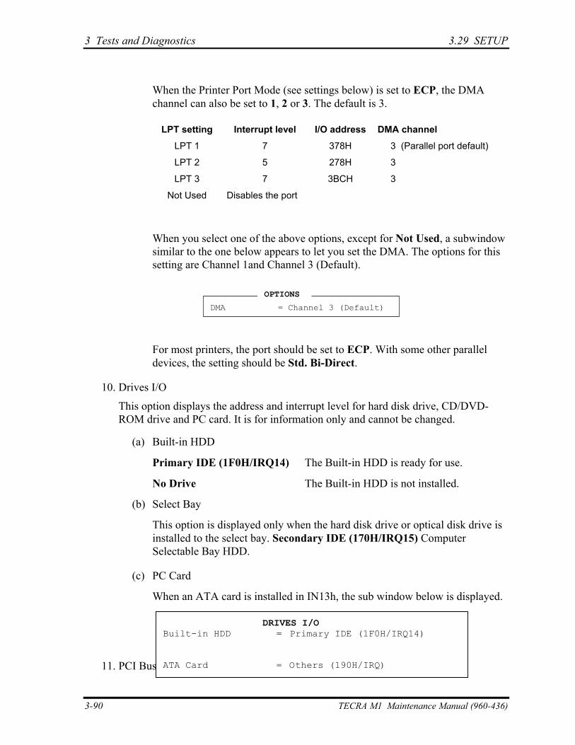
3 Tests and Diagnostics 3.29 SETUP
When the Printer Port Mode (see settings below) is set to ECP, the DMA channel can also be set to 1, 2 or 3. The default is 3.
LPT setting Interrupt level I/O address DMA channel LPT 1 7 378H 3 (Parallel port default)
LPT 2 5 278H 3
LPT 3 7 3BCH 3
Not Used Disables the port
When you select one of the above options, except for Not Used, a subwindow similar to the one below appears to let you set the DMA. The options for this setting are Channel 1and Channel 3 (Default).
DMA = Channel 3 (Default)
OPTIONS
For most printers, the port should be set to ECP. With some other parallel devices, the setting should be Std. Bi-Direct.
10. Drives I/O
This option displays the address and interrupt level for hard disk drive, CD/DVD-ROM drive and PC card. It is for information only and cannot be changed.
(a) Built-in HDD
Primary IDE (1F0H/IRQ14) The Built-in HDD is ready for use.
No Drive The Built-in HDD is not installed.
(b) Select Bay
This option is displayed only when the hard disk drive or optical disk drive is installed to the select bay. Secondary IDE (170H/IRQ15) Computer Selectable Bay HDD.
(c) PC Card
When an ATA card is installed in IN13h, the sub window below is displayed.
11. PCI Bus
3-90
Built-in HDD = Primary IDE (1F0H/IRQ14)
ATA Card = Others (190H/IRQ)
DRIVES I/O
TECRA M1 Maintenance Manual (960-436)
3.29 SETUP 3 Tests and Diagnostics
This item displays the interrupt level for the Card Bus. It is for information only and cannot be changed.
PCI BUS = IRQ11
12. PC Card
This option sets the PC Card Controller mode. This option can be changed when “Device Config.” is set to “All Devices”.
Auto-Selected Use this setting for all PC Cards when OS supports Plug&Play. (Default)
PCIC Compatible Use this setting for PCIC compatible PC card.
CardBus/16-bit Use this setting when CardBus does not work properly in Auto-Selected”, or PC card supports 16-bit.
13. Peripheral
Use this option to select the parallel port mode and hard disk mode.
(a) Internal Pointing Device
This option enables and disables the Touch Pad.
Enabled Enables the Touch Pad. (Default)
Disabled Disables the Touch Pad.
(b) Ext Keyboard "Fn"
Use this option to set the Fn key equivalent when you are using an external keyboard. Selecting this option displays the following subwindow.
Enabled Enables the feature.
Use the Fwill the F
Left Righ
TECRA M1 Maintenan
KEYBOARD
Ext Keyboard "Fn" key equivalent = Left Ctrl + Left Alt
this optin key o
enable yn key.
Ctrl + t Ctrl +
ce Manu
on to set a key combination on an external keyboard to emulate n the computer's internal keyboard. Setting an Fn key equivalent ou to use “Hotkeys” by pressing the set combination in place of
The following items can be selected for this option:
Left Alt* Right Alt*
al (960-436) 3-91
3 Tests and Diagnostics 3.29 SETUP
Left Alt + Left Shift Right Alt + Right Shift Left Alt + Caps Lock
*If these selections are made, you cannot warm boot the system by pressing Ctrl + Alt + Del.
Disabled Disables the feature. (Default)
(c) Parallel Port Mode
The options in this tab are ECP and Standard Bi-directional.
ECP Sets the port mode to Extended Capabilities Port (ECP). For most printers, the port should be set to ECP. (Default)
Std. Bi-Direct. This setting should be used with some other parallel devices.
(d) Hard Disk Mode
Use this item to select the hard disk mode.
Enhanced IDE Select this mode when using an operating system that (Normal) supports Enhanced IDE. (Default)
Standard IDE Select this mode when using an operating system that does not support Enhanced IDE.
NOTE: Formats for Enhanced IDE and Standard IDE are different, so if you change the setting, you will have to reformat the hard disk for the appropriate setting.
14. Legacy Emulation.
(a) USB keyboard/Mouse Legacy Emulation.
Use this option to enable or disable USB KB/Mouse Legacy Emulation. If your operating system does not support USB, you can still use a USB mouse and keyboard by setting the USB KB/Mouse Legacy Emulation item to Enabled.
Enabled USB Legacy Support can be used. (Default)
Disabled USB Legacy Support cannot be used.
(b) USB-FDD Legacy Emulation.
Use this option to enable or disable USB-FDD Legacy Emulation.
3-92 TECRA M1 Maintenance Manual (960-436)
3.29 SETUP 3 Tests and Diagnostics
Enabled USB Legacy Support can be used. (Default)
Disabled USB Legacy Support cannot be used.
15. PCI LAN (Not used)
This option enables/disables the Built-in LAN functions.
(a) Built-in LAN
Enabled Enables Built-in LAN functions. (Default)
Disabled Disables Built-in LAN functions.
16. HDD Password
This option sets HDD password. HDD password is a security function to protect the built-in HDD.
(a) HDD
This item selects the hard disk to set HDD password.
Built-in HDD Sets HDD password for the built-in HDD (Default)
Second HDD Sets HDD password for the second HDD
(b) HDD Password Mode
This item registers HDD password and can be selected only for registering HDD password. To change HDD Password Mode when HDD password is registered, delete the registered HDD password first, and then register new password.
User Only Sets only User HDD Password (Default)
Master+User Sets Master HDD Password and User HDD Password
(c) User Password
This item sets User password. For details on setting user password, refer to the User’s Manual.
TECRA M1 Maintenance Manual (960-436) 3-93
3 Tests and Diagnostics 3.29 SETUP
3-94 TECRA M1 Maintenance Manual (960-436)
Chapter 4 Replacement Procedures
4 Replacement Procedures
4-ii TECRA M1 Maintenance Manual (960-436)
4 Replacement Procedures
Chapter 4 Contents
4.1 General....................................................................................................................... 4-1
4.2 Battery Pack............................................................................................................... 4-9
4.3 Optional PC Card..................................................................................................... 4-12
4.4 Optional SD Card..................................................................................................... 4-14
4.5 HDD......................................................................................................................... 4-15
4.6 Slim Select Bay Module .......................................................................................... 4-20
4.7 Modem Daughter Card ............................................................................................ 4-24 4.8 CPU.......................................................................................................................... 4-27 4.9 Keyboard.................................................................................................................. 4-32 4.10 Memory Module ...................................................................................................... 4-36 4.11 Sensor/Switch Board................................................................................................ 4-38 4.12 Touch Pad ................................................................................................................ 4-40 4.13 Wireless LAN Card.................................................................................................. 4-44 4.14 Bluetooth Module .................................................................................................... 4-47 4.15 Display Assembly .................................................................................................... 4-49 4.16 LED Board ............................................................................................................... 4-53 4.17 Sound Board............................................................................................................. 4-55 4.18 System Board/RTC Battery/DC-IN Jack ................................................................. 4-57
4.19 USB Board ............................................................................................................... 4-62
4.20 Fan............................................................................................................................ 4-64
4.21 Display Mask ........................................................................................................... 4-66
4.22 FL Inverter ............................................................................................................... 4-68
4.23 LCD Module ............................................................................................................ 4-70
4.24 Wireless LAN Antenna/Bluetooth Antenna/Display Cover/Speaker ...................... 4-74
4.25 Fluorescent Lamp..................................................................................................... 4-85
4.25.1 Replacing the 14.1 Inch XGA TOSHIBA Fluorescent Lamp ................................. 4-86
4.25.2 Replacing the 14.1 Inch SXGA+ Sharp Fluorescent Lamp..................................... 4-98
TECRA M1 Maintenance Manual (960-436) 4-iii
4 Replacement Procedures
Figures
Figure 4-1 Releasing the Battery pack .......................................................................... 4-10
Figure 4-2 Removing a PC card .................................................................................... 4-12
Figure 4-3 Removing an SD card .................................................................................. 4-14
Figure 4-4 Removing the HDD cover ........................................................................... 4-16
Figure 4-5 Removing the HDD pack............................................................................. 4-17
Figure 4-6 Removing the HDD bracket......................................................................... 4-18
Figure 4-7 Removing the Slim select bay module......................................................... 4-21
Figure 4-8 Disassembling the Slim select bay module.................................................. 4-22
Figure 4-9 Removing the Modem daughter card cover................................................. 4-24
Figure 4-10 Removing the Modem daughter card........................................................... 4-25
Figure 4-11 Removing the CPU cover ............................................................................ 4-27
Figure 4-12 Removing the Fin......................................................................................... 4-28
Figure 4-13 Unlocking the CPU...................................................................................... 4-29
Figure 4-14 Applying new grease ................................................................................... 4-30
Figure 4-15 Removing the Keyboard brace..................................................................... 4-32
Figure 4-16 Removing the Keyboard .............................................................................. 4-33
Figure 4-17 Removing the Keyboard support plate ........................................................ 4-34
Figure 4-18 Removing the Memory module ................................................................... 4-36
Figure 4-19 Removing the Sensor/Switch board............................................................. 4-38
Figure 4-20 Removing the Palm rest (1) ......................................................................... 4-40
Figure 4-21 Removing the Palm rest (2) ......................................................................... 4-41
Figure 4-22 Removing the Touch pad and Touch pad switch......................................... 4-42
Figure 4-23 Removing the Wireless LAN card cover ..................................................... 4-44
Figure 4-24 Removing the Wireless LAN card............................................................... 4-45
Figure 4-25 Removing the Bluetooth module ................................................................. 4-48
Figure 4-26 Removing the Display assembly (1) ............................................................ 4-49
Figure 4-27 Removing the Display assembly (2) ............................................................ 4-50
Figure 4-28 Removing the Display assembly (3) ............................................................ 4-51
Figure 4-29 Removing the LED board ............................................................................ 4-53
4-iv TECRA M1 Maintenance Manual (960-436)
4 Replacement Procedures
Figure 4-30 Removing the Sound board.......................................................................... 4-55
Figure 4-31 Removing the System board/RTC battery/DC-IN jack (1) ......................... 4-58
Figure 4-32 Removing the System board/RTC battery/DC-IN jack (2) ......................... 4-59
Figure 4-33 Removing the DC-IN jack ........................................................................... 4-60
Figure 4-34 Removing the USB board ............................................................................ 4-62
Figure 4-35 Removing the Fan ........................................................................................ 4-64
Figure 4-36 Removing the Display mask (1) .................................................................. 4-66
Figure 4-37 Removing the Display mask (2) .................................................................. 4-67
Figure 4-38 Removing the FL inverter............................................................................ 4-68
Figure 4-39 Removing the LCD module (1) ................................................................... 4-71
Figure 4-40 Removing the LCD module (2) ................................................................... 4-72
Figure 4-41 Removing the Insulator................................................................................ 4-74
Figure 4-42 Removing the Cable holder ......................................................................... 4-75
Figure 4-43 Removing the cables .................................................................................... 4-76
Figure 4-44 Removing the Hinge (1)............................................................................... 4-77
Figure 4-45 Removing the Wireless LAN/Bluetooth antenna ........................................ 4-78
Figure 4-46 Removing the LCD cable............................................................................. 4-79
Figure 4-47 Removing the Speaker cable........................................................................ 4-80
Figure 4-48 Removing the Speaker and Side cover ........................................................ 4-81
Figure 4-49 Removing the Hinge (2)............................................................................... 4-82
Figure 4-50 Installing the Wireless LAN/Bluetooth antenna.......................................... 4-83
Figure 4-51 Replacing TOSHIBA fluorescent lamp (XGA) (1) ..................................... 4-87
Figure 4-52 Replacing TOSHIBA fluorescent lamp (XGA) (2) ..................................... 4-88
Figure 4-53 Replacing TOSHIBA fluorescent lamp (XGA) (3) ..................................... 4-89
Figure 4-54 Replacing TOSHIBA fluorescent lamp (XGA) (4) ..................................... 4-90
Figure 4-55 Replacing TOSHIBA fluorescent lamp (XGA) (5) ..................................... 4-91
Figure 4-56 Replacing TOSHIBA fluorescent lamp (XGA) (6) ..................................... 4-92
Figure 4-57 Replacing TOSHIBA fluorescent lamp (XGA) (7) ..................................... 4-93
Figure 4-58 Replacing TOSHIBA fluorescent lamp (XGA) (8) ..................................... 4-94
Figure 4-59 Replacing TOSHIBA fluorescent lamp (XGA) (9) ..................................... 4-95
Figure 4-60 Replacing TOSHIBA fluorescent lamp (XGA) (10) ................................... 4-96
Figure 4-61 Replacing TOSHIBA fluorescent lamp (XGA) (11) ................................... 4-97
TECRA M1 Maintenance Manual (960-436) 4-v
4 Replacement Procedures
4-vi TECRA M1 Maintenance Manual (960-436)
Figure 4-62 Replacing Sharp fluorescent lamp (SXGA+) (1)......................................... 4-98
Figure 4-63 Replacing Sharp fluorescent lamp (SXGA+) (2)......................................... 4-99
Figure 4-64 Replacing Sharp fluorescent lamp (SXGA+) (3)....................................... 4-100
Figure 4-65 Replacing Sharp fluorescent lamp (SXGA+) (4)....................................... 4-101
Figure 4-66 Replacing Sharp fluorescent lamp (SXGA+) (5)....................................... 4-102
Figure 4-67 Replacing Sharp fluorescent lamp (SXGA+) (6)....................................... 4-103
Figure 4-68 Replacing Sharp fluorescent lamp (SXGA+) (7)....................................... 4-104
Figure 4-69 Replacing Sharp fluorescent lamp (SXGA+) (8)....................................... 4-105
Figure 4-70 Replacing Sharp fluorescent lamp (SXGA+) (9)....................................... 4-106
Figure 4-71 Replacing Sharp fluorescent lamp (SXGA+) (10)..................................... 4-107
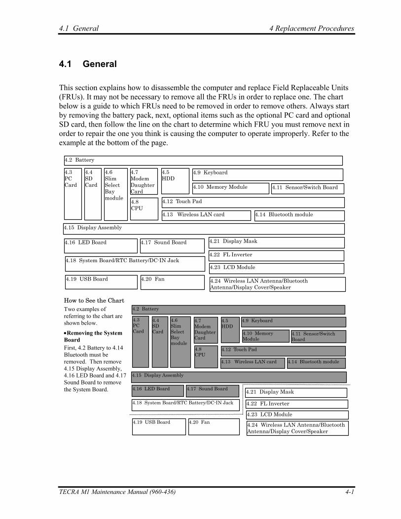
4.1 General 4 Replacement Procedures
4 Replacement Procedures
4.1 General
This section explains how to disassemble the computer and replace Field Replaceable Units (FRUs). It may not be necessary to remove all the FRUs in order to replace one. The chart below is a guide to which FRUs need to be removed in order to remove others. Always start by removing the battery pack, next, optional items such as the optional PC card and optional SD card, then follow the line on the chart to determine which FRU you must remove next in order to repair the one you think is causing the computer to operate improperly. Refer to the example at the bottom of the page.
How to See the ChartTwo examples ofreferring to the chart areshown below.
•Removing the SystemBoardFirst, 4.2 Battery to 4.14Bluetooth must beremoved. Then remove4.15 Display Assembly,4.16 LED Board and 4.17Sound Board to removethe System Board.
4.2 Battery
4.3PCCard
4.4SDCard
4.6SlimSelectBaymodule
4.5HDD
4.7ModemDaughterCard
4.20 Fan
4.8CPU
4.9 Keyboard
4.10 Memory Module
4.13 Wireless LAN card 4.14 Bluetooth module
4.11 Sensor/Switch Board
4.15 Display Assembly
4.12 Touch Pad
4.16 LED Board
4.19 USB Board
4.17 Sound Board 4.21 Display Mask
4.22 FL Inverter
4.23 LCD Module
4.24 Wireless LAN Antenna/BluetoothAntenna/Display Cover/Speaker
4.18 System Board/RTC Battery/DC-IN Jack
4.2 Battery
4.3PCCard
4.4SDCard
4.6SlimSelectBaymodule
4.5HDD
4.7ModemDaughterCard
4.20 Fan
4.8CPU
4.9 Keyboard
4.10 MemoryModule
4.13 Wireless LAN card 4.14 Bluetooth module
4.11 Sensor/SwitchBoard
4.15 Display Assembly
4.12 Touch Pad
4.16 LED Board
4.19 USB Board
4.17 Sound Board 4.21 Display Mask
4.22 FL Inverter
4.23 LCD Module
4.24 Wireless LAN Antenna/BluetoothAntenna/Display Cover/Speaker
4.18 System Board/RTC Battery/DC-IN Jack
TECRA M1 Maintenance Manual (960-436) 4-1
4 Replacement Procedures 4.1 General
Safety Precautions
Before you begin disassembly, read the following safety precautions and observe them carefully as you work.
DANGER: 1) Always use the genuine battery that is authorized by Toshiba or compatible with the unit. Since other battery packs have different specifications, they may be incompatible with the unit, and may burst or explode. Never heat or disassemble the battery pack, as that could cause leakage of alkaline solution. Never throw the battery pack into a fire, as that could cause the battery pack to explode.
2) The power supply, FL inverter and other components carry high voltages. If you need to turn on the power of a partially disassembled computer to check its operation, be very careful not to touch connectors or components, in order to avoid the risk of electric shock. Also, do not disassemble individual components in first-level maintenance.
WARNING: 1) Turn off the power and disconnect the AC adaptor from the power source, to avoid exposure to electric shock.
2) Batteries in the computer retain an electrical charge, so there is danger of electrical shock even when the computer is disconnected from an AC power source. Remove any metal jewelry or accessories such as necklaces, bracelets or rings, in order to reduce the risk of electric shock. Never work with wet or damp hands.
3) Be careful of edges and corners as these may cut.
CAUTION: 1) When you change a component, be sure the replacement component meets the required specifications. Never use foreign parts, to avoid any risk of damage to the computer.
2) To avoid any risk of short-circuit, fire or other internal damage, never allow any metal objects such as screws or paper clips to fall into the unit. Be sure to replace screws with the same size as those removed. Make sure all screws are securely fastened. Loose screws can cause short circuits, resulting in heat, smoke or fire.
3) Before lifting out an FRU or other component, make sure all cables to the component have been disconnected, in order to reduce the risk of accidental electric shock.
4) If you use AC power, be sure to use the cable that came with the computer or one recommended by Toshiba.
5) Make sure that all replacement components meet the specifications for the computer and that all cables and connectors are securely fastened, in order to avoid the risk of electric shock.
6) Some parts inside the computer, such as the CPU and cooling module, become very hot during operation. Conduct repair work after they have cooled. Be careful around the CPU and cooling module to avoid burns.
4-2 TECRA M1 Maintenance Manual (960-436)
4.1 General 4 Replacement Procedures
Before You Begin
Look over the procedures in this section before you begin disassembling the computer. Familiarize yourself with the disassembly and reassembly steps. Begin each procedure by removing the AC adapter and the battery pack as instructed in this section:
1. Do not disassemble the computer unless it is operating abnormally.
2. Use only the correct and approved tools.
3. Make sure the working environment is free from the following elements whether you are using or storing the computer.
• Dust and contaminates • Static electricity • Extreme heat, cold and humidity
4. Make sure the FRU you are replacing is causing the abnormal operation by performing the necessary diagnostics tests described in this manual.
5. Do not perform any operations that are not necessary and use only the described procedures for disassembling and installing FRUs in the computer.
6. After removing parts from the computer, place them in a safe place away from the computer so they will not be damaged and will not interfere with your work.
7. You will remove and replace many screws when you disassemble the computer. When you remove screws, make sure they are placed in a safe place and identified with the correct parts.
8. When assembling the computer make sure you use the correct screws to secure the various pieces in place. Screw sizes are listed in their corresponding figures.
9. The computer contains many sharp edges and corners, so be careful not to injure yourself.
10. After you have replaced an FRU, make sure the computer is functioning properly by performing the appropriate test on the FRU you have fixed or replaced.
TECRA M1 Maintenance Manual (960-436) 4-3
4 Replacement Procedures 4.1 General
Disassembly Procedures
The computer has two basic types of cable connectors:
• Pressure Plate Connectors • Coaxial Cable Connectors • Normal Pin Connectors
To disconnect a Pressure Plate connector, lift up the tabs on either side of the connector’s plastic pressure plate and slide the cable out of the connector. To connect the cable to a Pressure Plate connector, make sure the pressure plate is fully lifted and slide the cable into the connector. Secure the cable in place by pushing the sides of the pressure plate down so the plate is flush with the sides of the connector. Gently pull on the cable to make sure the cable is secure. If you pull out the connector, connect it again making sure the connector’s pressure plate is fully lifted when you insert the cable.
Coaxial cables should be disconnected with an antenna coaxial disconnector.
Standard pin connectors are used with all other cables. These connectors can be connected and disconnected by simply pulling them apart or pushing them together.
Assembly Procedures
After you have disassembled the computer and fixed or repaired the problem that was causing the computer to operate abnormally, you will need to reassemble the computer.
Install all the removed FRUs following the steps described in the corresponding sections in this chapter.
While assembling the computer, remember the following general points:
• Take your time, making sure you follow the instructions closely. Most problems arise when you get in a hurry assembling the computer.
• Make sure all cables and connectors are securely fastened.
• Before securing the FRU or other parts, make sure that screws or the FRU will pinch no cables.
• Check that all latches are closed securely in place.
• Make sure all the correct screws are used to secure all FRUs. Using the wrong screw can either damage the threads on the screw or the head of the screw and may prevent proper seating of an FRU.
After installing an FRU in the computer, confirm that the FRU and the computer are functioning properly.
4-4 TECRA M1 Maintenance Manual (960-436)
4.1 General 4 Replacement Procedures
Tools and Equipment
The use of Electrostatic Discharge (ESD) equipment is very important for your safety and the safety of those around you. Proper use of these devices will increase the success rate of your repairs and lower the cost for damaged or destroyed parts. The following equipment is necessary to disassemble and reassemble the computer:
• One M2 point size 0 Phillips screwdriver to remove and replace screws.
• One 4 mm flat-blade screwdriver.
• Tweezers, to lift out screws that you cannot grasp with your fingers.
• ESD mats for the floor and the table you are working on.
• An ESD wrist strap or heel grounder.
• Anti-static carpeting or flooring.
• Air ionizers in highly static sensitive areas.
• Plastic card of the size of credit card.
• Antenna coaxial cable disconnector
TECRA M1 Maintenance Manual (960-436) 4-5
4 Replacement Procedures 4.1 General
Screw Tightening Torque
When you fasten screws, be sure to follow the torque list below.
CAUTION: Overtightening can damage components and screws; undertightening can result in electrical shorts or other damage if screws or components come loose.
NOTE: Toshiba recommends that you use an electric screw driver for quick and easy operations.
• M2 0.17 N·m (1.7 kgf·cm)
• M2.5 0.30 N·m (3.0 kgf·cm)
• M3 0.57 N·m (5.6 kgf·cm)
NOTE: The computer contains several flat head screws. These screws have less contact area with the screwdriver, so be careful to press firmly enough to prevent the screwdriver from slipping out and damaging the screw head.
4-6 TECRA M1 Maintenance Manual (960-436)
4.1 General 4 Replacement Procedures
Color of Screw Shaft
To avoid mistakes on the screw length, screw shafts are colored as follows:
Even number length screw: brown
Odd number length screw: white
Special length screw: blue Screws whose lengths are indicated to one or more decimal places such as 2.5 mm or 2.8 mm.
Marking of Screws on the Computer Body
To make maintenance of the computer easier, markings of the kinds of the screws including the types and lengths of the screws are indicated on the computer body.
Kind of screws Symbol
BIND screw B
FLAT HEAD screw F
SUPER FLAT HEAD screw S
TAPPING screw T
Other screws U (Unique screws, STUD, etc.)
Examples:
6 mm BIND screw B6
12 mm BIND screw B12
5 mm FLAT HEAD screw F5
(Indicates the screwed length in round number regardless the length of the stud.)
TECRA M1 Maintenance Manual (960-436) 4-7
4 Replacement Procedures 4.2 Battery Pack
4.2 Battery Pack
Removing the Battery Pack
To remove the battery pack, follow the steps below and refer to figure 4-1.
CAUTION: When handling battery packs, be careful not to short circuit the terminals. Also do not drop, hit or apply impact; do not scratch, break, twist or bend the battery pack.
1. Turn off the computer.
2. Disconnect the AC cable and other external devices from the computer.
3. Turn the computer face down.
4-8 TECRA M1 Maintenance Manual (960-436)
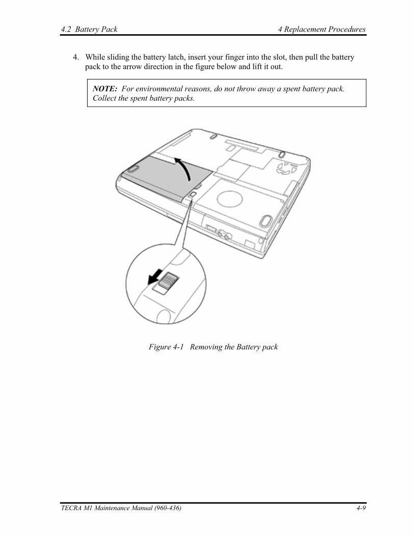
4.2 Battery Pack 4 Replacement Procedures
4. While sliding the battery latch, insert your finger into the slot, then pull the battery pack to the arrow direction in the figure below and lift it out.
NOTE: For environmental reasons, do not throw away a spent battery pack. Collect the spent battery packs.
Figure 4-1 Removing the Battery pack
TECRA M1 Maintenance Manual (960-436) 4-9
4 Replacement Procedures 4.2 Battery Pack
Installing the Battery Pack
To install the battery pack, follow the steps below and refer to figure 4-1.
CAUTION: The battery pack is a lithium ion battery, which can explode if not properly replaced, used, handled or disposed of. For environmental reasons, collect the spent battery packs. Use only batteries recommended by Toshiba as replacements.
NOTE: Check the battery's terminals visually. If they are dirty, wipe them clean with a dry cloth.
1. Insert the battery pack into the opposite side of the battery connector.
2. Push the battery pack toward the connector. Make sure the battery pack is installed securely.
4-10 TECRA M1 Maintenance Manual (960-436)
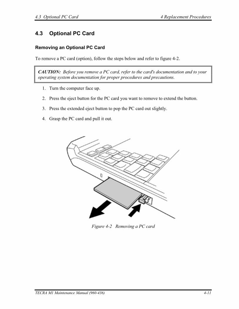
4.3 Optional PC Card 4 Replacement Procedures
4.3 Optional PC Card
Removing an Optional PC Card
To remove a PC card (option), follow the steps below and refer to figure 4-2.
CAUTION: Before you remove a PC card, refer to the card's documentation and to your operating system documentation for proper procedures and precautions.
1. Turn the computer face up.
2. Press the eject button for the PC card you want to remove to extend the button.
3. Press the extended eject button to pop the PC card out slightly.
4. Grasp the PC card and pull it out.
Figure 4-2 Removing a PC card
TECRA M1 Maintenance Manual (960-436) 4-11
4 Replacement Procedures 4.3 Optional PC Card
Installing an Optional PC Card
To install a PC card, follow the steps below and refer to figure 4-2.
1. Insert a PC card.
2. Push it carefully to ensure a firm connection.
4-12 TECRA M1 Maintenance Manual (960-436)
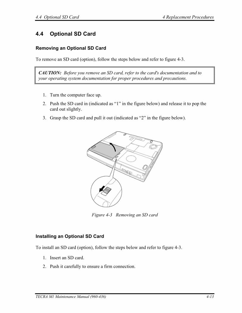
4.4 Optional SD Card 4 Replacement Procedures
4.4 Optional SD Card
Removing an Optional SD Card
To remove an SD card (option), follow the steps below and refer to figure 4-3.
CAUTION: Before you remove an SD card, refer to the card's documentation and to your operating system documentation for proper procedures and precautions.
1. Turn the computer face up.
2. Push the SD card in (indicated as “1” in the figure below) and release it to pop the card out slightly.
3. Grasp the SD card and pull it out (indicated as “2” in the figure below).
Figure 4-3 Removing an SD card
Installing an Optional SD Card
To install an SD card (option), follow the steps below and refer to figure 4-3.
1. Insert an SD card.
2. Push it carefully to ensure a firm connection.
TECRA M1 Maintenance Manual (960-436) 4-13
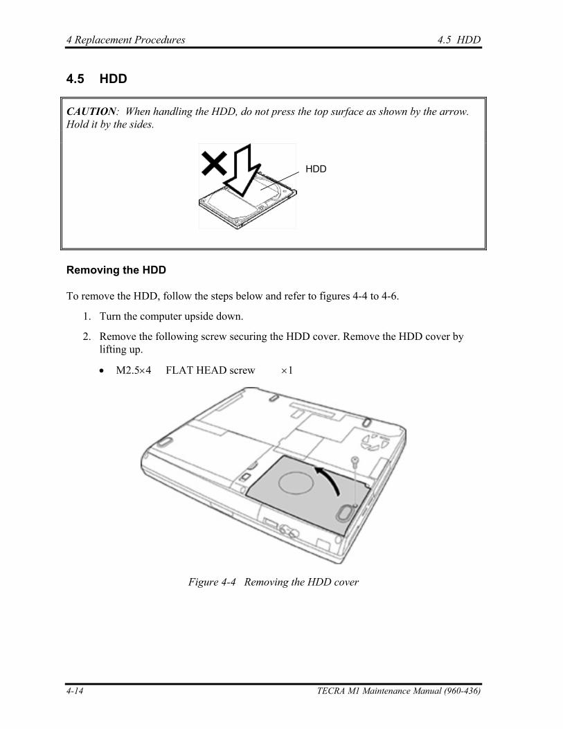
4 Replacement Procedures 4.5 HDD
4.5 HDD
CAUTION: When handling the HDD, do not press the top surface as shown by the arrow. Hold it by the sides.
HDD
Removing the HDD
To remove the HDD, follow the steps below and refer to figures 4-4 to 4-6.
1. Turn the computer upside down.
2. Remove the following screw securing the HDD cover. Remove the HDD cover by lifting up.
• M2.5×4 FLAT HEAD screw ×1
Figure 4-4 Removing the HDD cover
4-14 TECRA M1 Maintenance Manual (960-436)
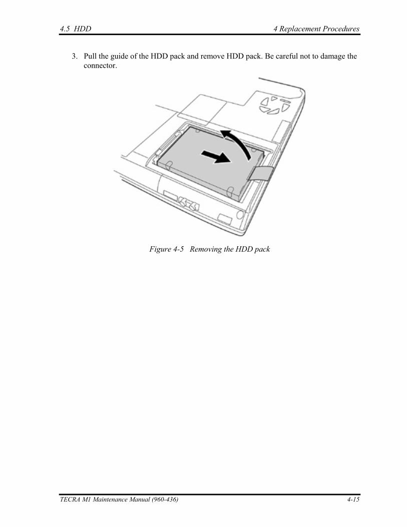
4.5 HDD 4 Replacement Procedures
3. Pull the guide of the HDD pack and remove HDD pack. Be careful not to damage the connector.
Figure 4-5 Removing the HDD pack
TECRA M1 Maintenance Manual (960-436) 4-15
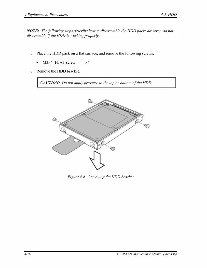
4 Replacement Procedures 4.5 HDD
NOTE: The following steps describe how to disassemble the HDD pack; however, do not disassemble if the HDD is working properly.
5. Place the HDD pack on a flat surface, and remove the following screws.
• M3×4 FLAT screw ×4
6. Remove the HDD bracket.
CAUTION: Do not apply pressure to the top or bottom of the HDD.
Figure 4-6 Removing the HDD bracket
4-16 TECRA M1 Maintenance Manual (960-436)
4.5 HDD 4 Replacement Procedures
Installing the HDD
To install the HDD, follow the steps below and refer to figures 4-4 to 4-6.
CAUTION: Do not hold the HDD by its top and bottom flat surfaces. It may damage the HDD.
1. Seat the HDD in the bracket.
2. Secure the HDD to the HDD bracket with the following screws.
• M3×4 FLAT screw ×4
CAUTION: Do not apply pressure to the middle of the HDD pack. It may damage the HDD pack. Hold the HDD pack by its corners.
3. Hold the HDD pack by its corners and place it in the dent. Slide the HDD pack to the connector of the computer to connect. Press to ensure a firm connection.
4. Fold the guide not to cover the screw hole on the HDD cover. Seat the HDD cover and secure it with the following screw.
• M2.5×4 FLAT HEAD screw ×1
TECRA M1 Maintenance Manual (960-436) 4-17
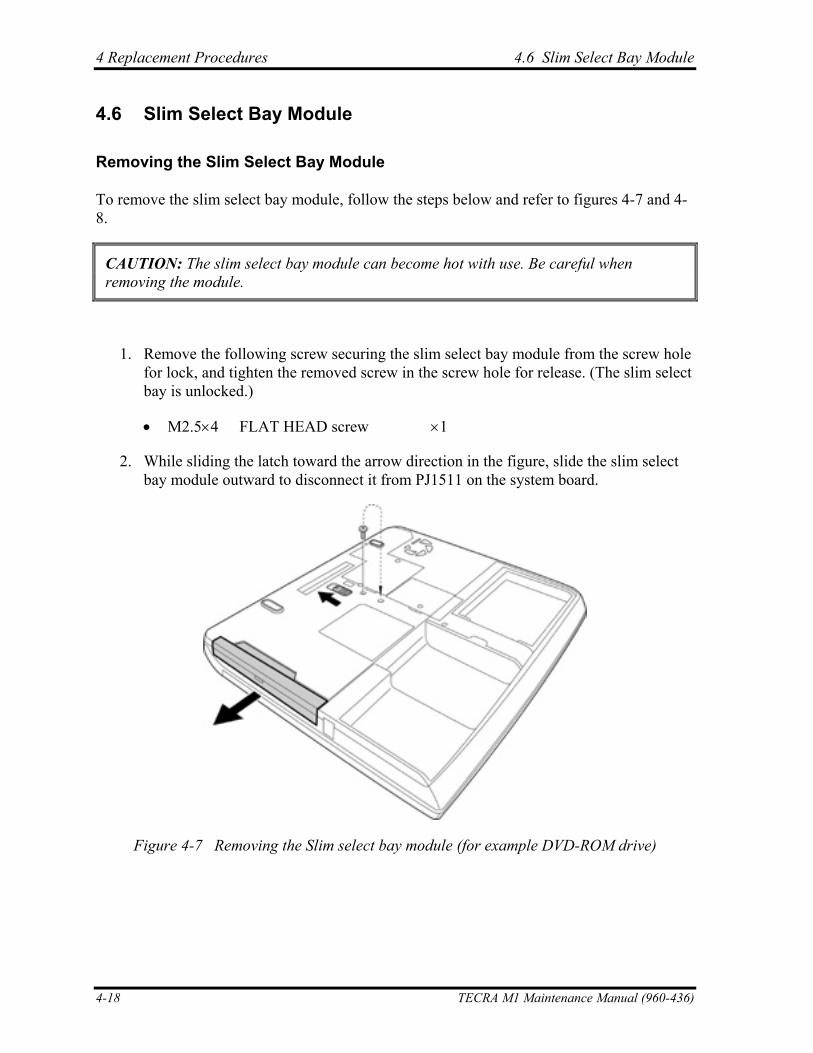
4 Replacement Procedures 4.6 Slim Select Bay Module
4.6 Slim Select Bay Module
Removing the Slim Select Bay Module
To remove the slim select bay module, follow the steps below and refer to figures 4-7 and 4-8.
CAUTION: The slim select bay module can become hot with use. Be careful when removing the module.
1. Remove the following screw securing the slim select bay module from the screw hole for lock, and tighten the removed screw in the screw hole for release. (The slim select bay is unlocked.)
• M2.5×4 FLAT HEAD screw ×1
2. While sliding the latch toward the arrow direction in the figure, slide the slim select bay module outward to disconnect it from PJ1511 on the system board.
Figure 4-7 Removing the Slim select bay module (for example DVD-ROM drive)
4-18 TECRA M1 Maintenance Manual (960-436)
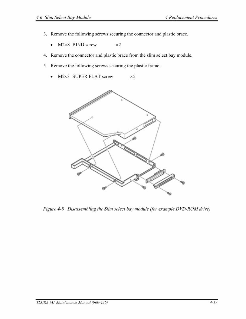
4.6 Slim Select Bay Module 4 Replacement Procedures
3. Remove the following screws securing the connector and plastic brace.
• M2×8 BIND screw ×2
4. Remove the connector and plastic brace from the slim select bay module.
5. Remove the following screws securing the plastic frame.
• M2×3 SUPER FLAT screw ×5
Figure 4-8 Disassembling the Slim select bay module (for example DVD-ROM drive)
TECRA M1 Maintenance Manual (960-436) 4-19
4 Replacement Procedures 4.6 Slim Select Bay Module
Installing the Slim Select Bay Module
To install the slim select bay module, follow the steps below and refer to figures 4-7 and 4-8.
1. Seat the plastic frame on the side of the slim select bay module, and secure it with the following screws.
• M2×3 SUPER FLAT screw ×5
2. Install the connector and plastic brace and secure them with the following screws.
• M2×8 BIND screw ×2
3. Slide the slim select bay module into the computer to connect it to PJ1511 on the system board.
4. Remove the following screw tightened when removing the slim select bay module. Then secure the removed screw in the next screw hole. (The slim select bay is locked.)
• M2.5×4 FLAT HEAD screw ×1
4-20 TECRA M1 Maintenance Manual (960-436)
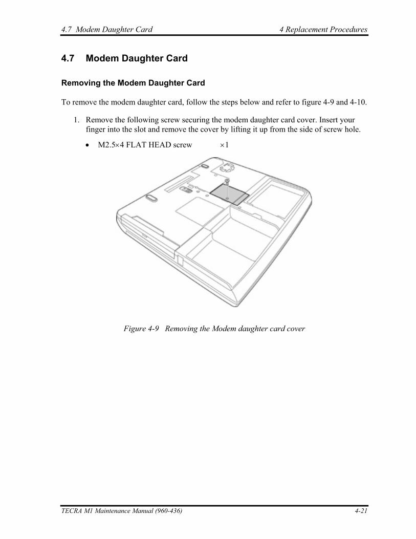
4.7 Modem Daughter Card 4 Replacement Procedures
4.7 Modem Daughter Card
Removing the Modem Daughter Card
To remove the modem daughter card, follow the steps below and refer to figure 4-9 and 4-10.
1. Remove the following screw securing the modem daughter card cover. Insert your finger into the slot and remove the cover by lifting it up from the side of screw hole.
• M2.5×4 FLAT HEAD screw ×1
Figure 4-9 Removing the Modem daughter card cover
TECRA M1 Maintenance Manual (960-436) 4-21
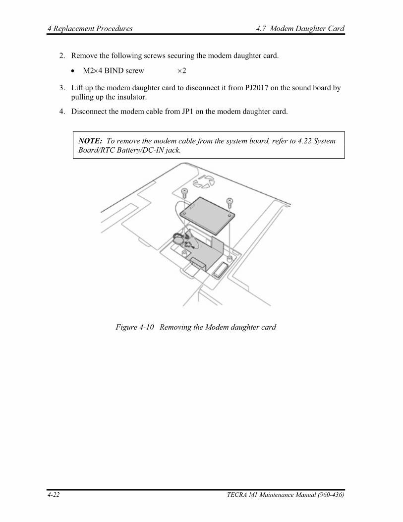
4 Replacement Procedures 4.7 Modem Daughter Card
2. Remove the following screws securing the modem daughter card.
• M2×4 BIND screw ×2
3. Lift up the modem daughter card to disconnect it from PJ2017 on the sound board by pulling up the insulator.
4. Disconnect the modem cable from JP1 on the modem daughter card.
NOTE: To remove the modem cable from the system board, refer to 4.22 System Board/RTC Battery/DC-IN jack.
Figure 4-10 Removing the Modem daughter card
4-22 TECRA M1 Maintenance Manual (960-436)
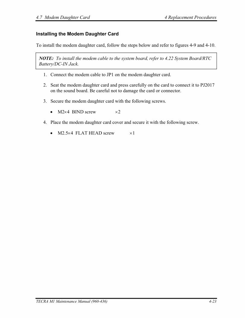
4.7 Modem Daughter Card 4 Replacement Procedures
Installing the Modem Daughter Card
To install the modem daughter card, follow the steps below and refer to figures 4-9 and 4-10.
NOTE: To install the modem cable to the system board, refer to 4.22 System Board/RTC Battery/DC-IN Jack.
1. Connect the modem cable to JP1 on the modem daughter card.
2. Seat the modem daughter card and press carefully on the card to connect it to PJ2017 on the sound board. Be careful not to damage the card or connector.
3. Secure the modem daughter card with the following screws.
• M2×4 BIND screw ×2
4. Place the modem daughter card cover and secure it with the following screw.
• M2.5×4 FLAT HEAD screw ×1
TECRA M1 Maintenance Manual (960-436) 4-23
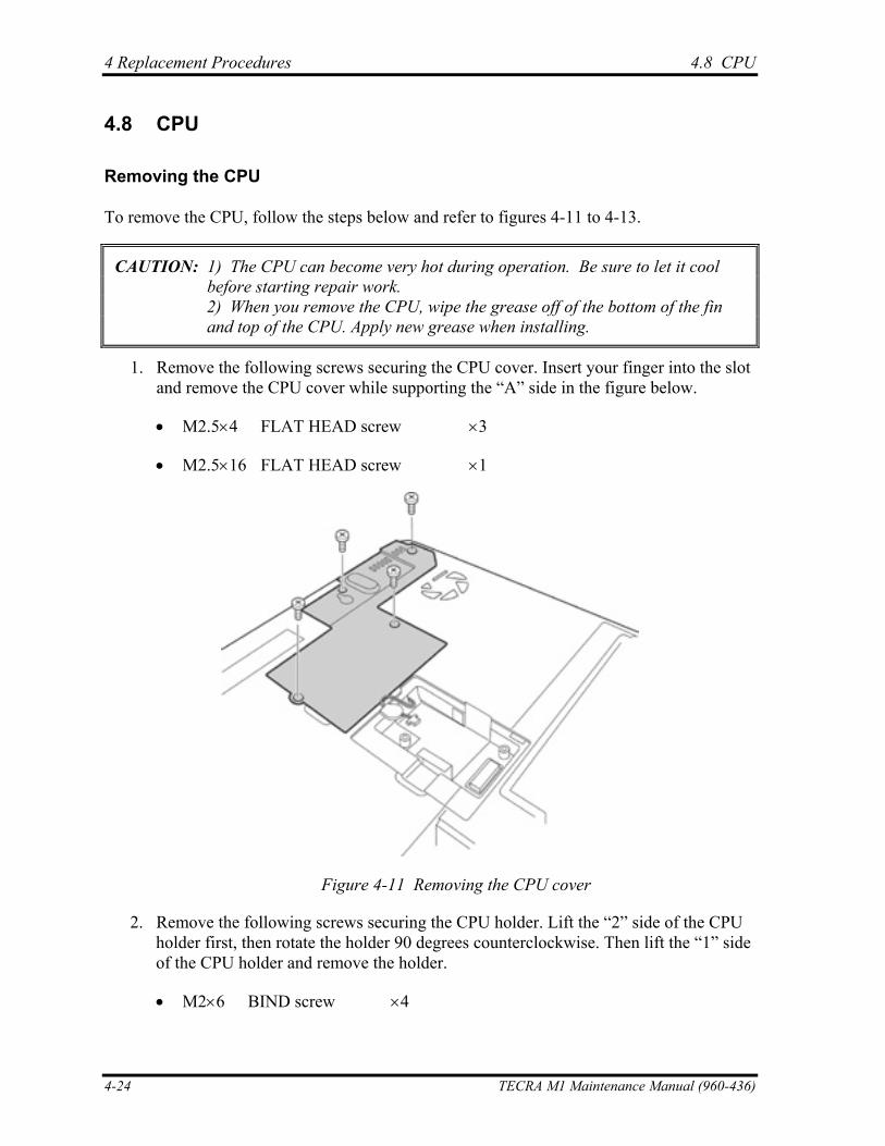
4 Replacement Procedures 4.8 CPU
4.8 CPU
Removing the CPU
To remove the CPU, follow the steps below and refer to figures 4-11 to 4-13.
CAUTION: 1) The CPU can become very hot during operation. Be sure to let it cool before starting repair work. 2) When you remove the CPU, wipe the grease off of the bottom of the fin and top of the CPU. Apply new grease when installing.
1. Remove the following screws securing the CPU cover. Insert your finger into the slot and remove the CPU cover while supporting the “A” side in the figure below.
• M2.5×4 FLAT HEAD screw ×3
• M2.5×16 FLAT HEAD screw ×1
Figure 4-11 Removing the CPU cover
2. Remove the following screws securing the CPU holder. Lift the “2” side of the CPU holder first, then rotate the holder 90 degrees counterclockwise. Then lift the “1” side of the CPU holder and remove the holder.
• M2×6 BIND screw ×4
4-24 TECRA M1 Maintenance Manual (960-436)
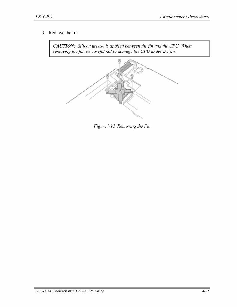
4.8 CPU 4 Replacement Procedures
3. Remove the fin.
CAUTION: Silicon grease is applied between the fin and the CPU. When removing the fin, be careful not to damage the CPU under the fin.
Figure4-12 Removing the Fin
TECRA M1 Maintenance Manual (960-436) 4-25
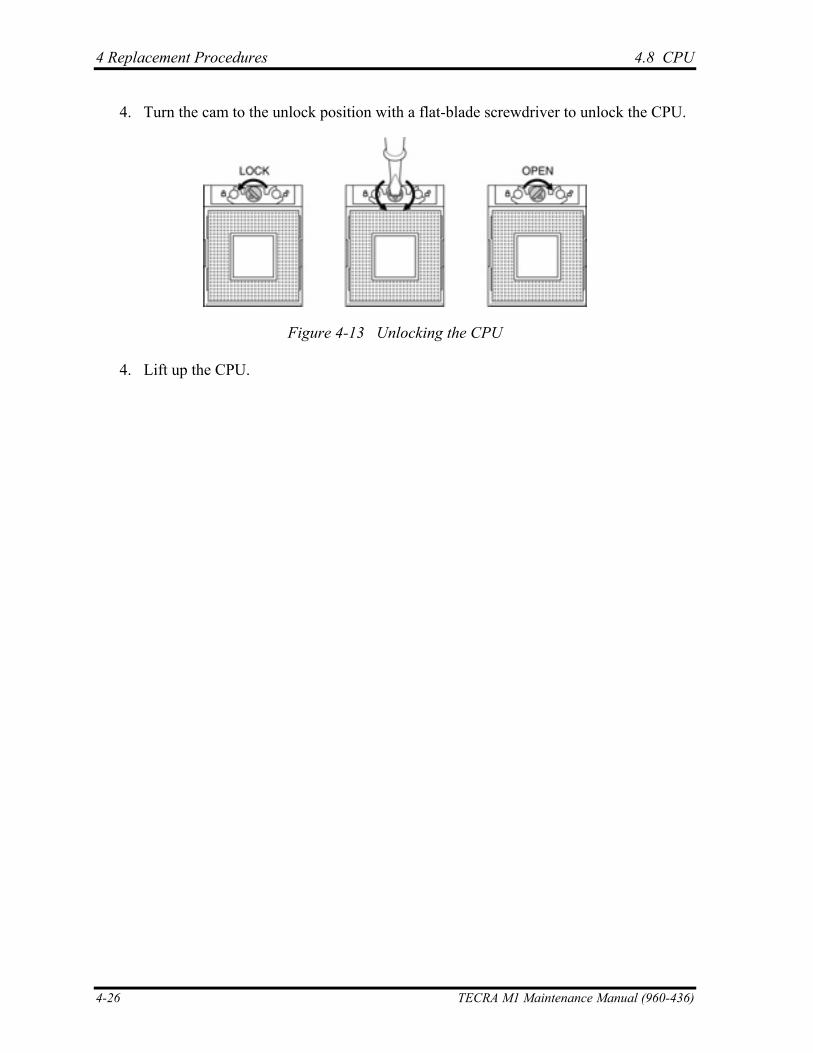
4 Replacement Procedures 4.8 CPU
4. Turn the cam to the unlock position with a flat-blade screwdriver to unlock the CPU.
Figure 4-13 Unlocking the CPU
4. Lift up the CPU.
4-26 TECRA M1 Maintenance Manual (960-436)
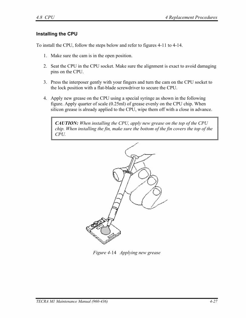
4.8 CPU 4 Replacement Procedures
Installing the CPU
To install the CPU, follow the steps below and refer to figures 4-11 to 4-14.
1. Make sure the cam is in the open position.
2. Seat the CPU in the CPU socket. Make sure the alignment is exact to avoid damaging pins on the CPU.
3. Press the interposer gently with your fingers and turn the cam on the CPU socket to the lock position with a flat-blade screwdriver to secure the CPU.
4. Apply new grease on the CPU using a special syringe as shown in the following figure. Apply quarter of scale (0.25ml) of grease evenly on the CPU chip. When silicon grease is already applied to the CPU, wipe them off with a close in advance.
CAUTION: When installing the CPU, apply new grease on the top of the CPU chip. When installing the fin, make sure the bottom of the fin covers the top of the CPU.
Figure 4-14 Applying new grease
TECRA M1 Maintenance Manual (960-436) 4-27
4 Replacement Procedures 4.8 CPU
4-28 TECRA M1 Maintenance Manual (960-436)
5. Install the fin.
6. Insert the “1” side of the CPU holder into the empty space, with rotated 90 degrees counterclockwise first. Then rotate it 90 degrees clockwise and fit the two holes of the CPU holder to the bosses on the fin.
7. Secure the CPU holder with the following screws.
• M2×6 BIND screw ×4
8. Place the CPU cover and secure it with the following screws.
• M2.5×4 FLAT HEAD screw ×3
• M2.5×16 FLAT HEAD screw ×1
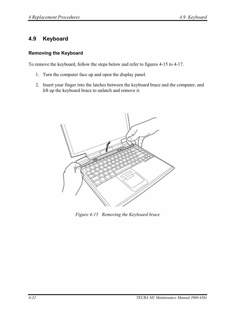
4 Replacement Procedures 4.9 Keyboard
4 Replacement Procedures
4.9 Keyboard
Removing the Keyboard
To remove the keyboard, follow the steps below and refer to figures 4-15 to 4-17.
1. Turn the computer face up and open the display panel.
2. Insert your finger into the latches between the keyboard brace and the computer, and lift up the keyboard brace to unlatch and remove it.
Figure 4-15 Removing the Keyboard brace
4-32 TECRA M1 Maintenance Manual (960-436)
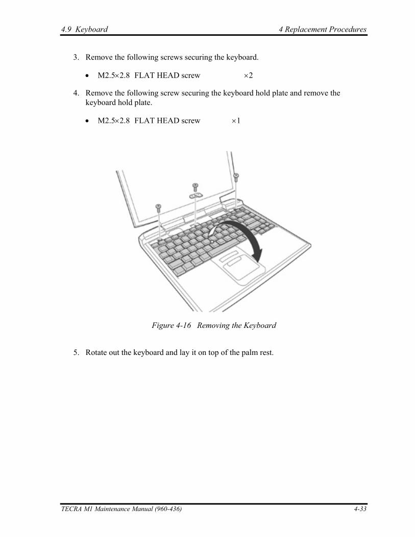
4.9 Keyboard 4 Replacement Procedures
3. Remove the following screws securing the keyboard.
• M2.5×2.8 FLAT HEAD screw ×2
4. Remove the following screw securing the keyboard hold plate and remove the keyboard hold plate.
• M2.5×2.8 FLAT HEAD screw ×1
Figure 4-16 Removing the Keyboard
5. Rotate out the keyboard and lay it on top of the palm rest.
TECRA M1 Maintenance Manual (960-436) 4-33
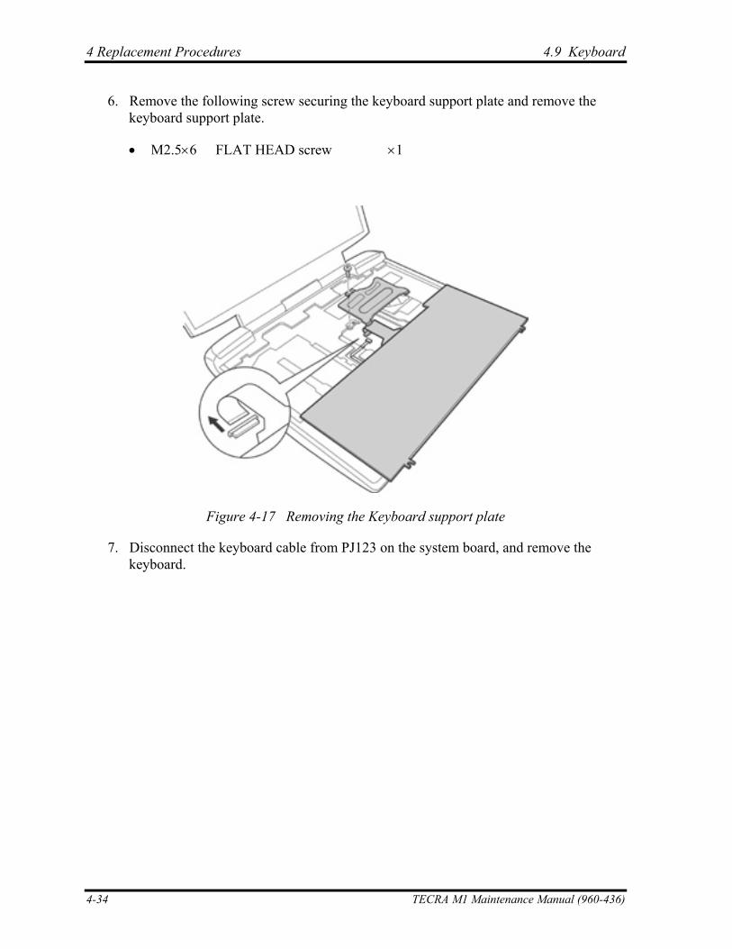
4 Replacement Procedures 4.9 Keyboard
6. Remove the following screw securing the keyboard support plate and remove the keyboard support plate.
• M2.5×6 FLAT HEAD screw ×1
Figure 4-17 Removing the Keyboard support plate
7. Disconnect the keyboard cable from PJ123 on the system board, and remove the keyboard.
4-34 TECRA M1 Maintenance Manual (960-436)
4.9 Keyboard 4 Replacement Procedures
Installing the Keyboard
To install the keyboard, follow the steps below and refer to figures 4-15 to 4-17.
1. Place the keyboard face down on the palm rest.
2. Connect the keyboard cable to PJ123 on the system board.
3. Insert the tabs on the keyboard support plate first, then place the keyboard support plate on the keyboard cable. Secure the keyboard support plate with the following screw.
• M2.5×6 FLAT HEAD screw ×1
4. Align the tabs on the bottom of the keyboard with the holes on the top cover and rotate the keyboard down.
5. Secure the keyboard with the following screws.
• M2.5×2.8 FLAT HEAD screw ×2
6. Place the keyboard hold plate on the keyboard. Then secure the keyboard hold plate with the following screw.
• M2.5×2.8 FLAT HEAD screw ×1
7. Install the keyboard brace and press to secure the latches.
TECRA M1 Maintenance Manual (960-436) 4-35
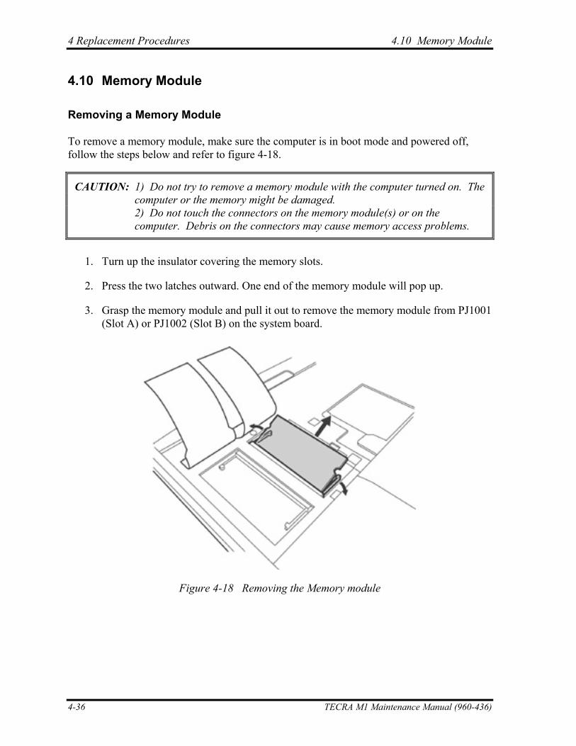
4 Replacement Procedures 4.10 Memory Module
4.10 Memory Module
Removing a Memory Module
To remove a memory module, make sure the computer is in boot mode and powered off, follow the steps below and refer to figure 4-18.
CAUTION: 1) Do not try to remove a memory module with the computer turned on. The computer or the memory might be damaged. 2) Do not touch the connectors on the memory module(s) or on the computer. Debris on the connectors may cause memory access problems.
1. Turn up the insulator covering the memory slots.
2. Press the two latches outward. One end of the memory module will pop up.
3. Grasp the memory module and pull it out to remove the memory module from PJ1001 (Slot A) or PJ1002 (Slot B) on the system board.
Figure 4-18 Removing the Memory module
4-36 TECRA M1 Maintenance Manual (960-436)
4.10 Memory Module 4 Replacement Procedures
Installing a Memory Module
To install a memory module, make sure that the computer is in boot mode and powered off, follow the steps below and refer to figure 4-18.
CAUTION: 1) Do not install a memory module in slot B only. Use slot A prior to slot B. Otherwise, the computer or the memory may be damaged.
2) Do not touch the connectors on the memory module or on the computer.
Debris on the connectors may cause memory access problems.
1. Turn up the insulator and insert a memory module into PJ1001 (Slot A) or PJ1002
(Slot B) on the system board at an angle of 45 degrees and press carefully to ensure firm connection.
2. Push the memory module down until the latches on either side engage the memory module to hold it in place.
3. Seat the insulator.
TECRA M1 Maintenance Manual (960-436) 4-37
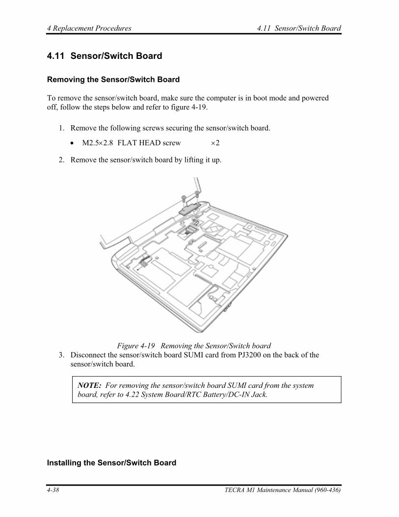
4 Replacement Procedures 4.11 Sensor/Switch Board
4.11 Sensor/Switch Board
Removing the Sensor/Switch Board
To remove the sensor/switch board, make sure the computer is in boot mode and powered off, follow the steps below and refer to figure 4-19.
1. Remove the following screws securing the sensor/switch board.
• M2.5×2.8 FLAT HEAD screw ×2
2. Remove the sensor/switch board by lifting it up.
Figure 4-19 Removing the Sensor/Switch board 3. Disconnect the sensor/switch board SUMI card from PJ3200 on the back of the
sensor/switch board.
NOTE: For removing the sensor/switch board SUMI card from the system board, refer to 4.22 System Board/RTC Battery/DC-IN Jack.
Installing the Sensor/Switch Board
4-38 TECRA M1 Maintenance Manual (960-436)
4.11 Sensor/Switch Board 4 Replacement Procedures
To install the sensor/switch board, make sure that the computer is in boot mode and powered off, follow the steps below and refer to figure 4-19.
NOTE: For installing the sensor/switch board SUMI card to the system board, refer to 4.22 System Board/RTC Battery/DC-IN Jack.
1. Connect the sensor/switch board SUMI card on the system board to PJ3200 on the back of the sensor/switch board.
2. Seat the sensor/switch board. Attach the two holes of the board to the bosses of the chassis.
3. Secure the sensor/switch board with the following screws.
• M2.5×2.8 FLAT HEAD screw ×2
TECRA M1 Maintenance Manual (960-436) 4-39
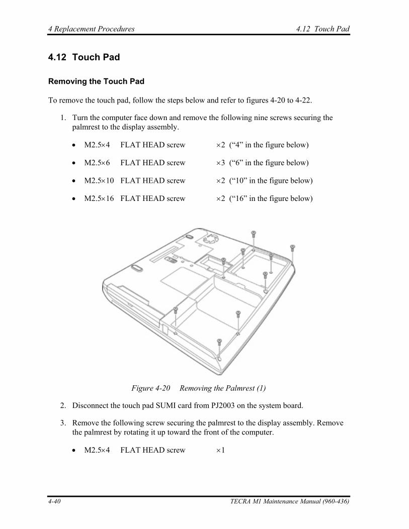
4 Replacement Procedures 4.12 Touch Pad
4.12 Touch Pad
Removing the Touch Pad
To remove the touch pad, follow the steps below and refer to figures 4-20 to 4-22.
1. Turn the computer face down and remove the following nine screws securing the palmrest to the display assembly.
• M2.5×4 FLAT HEAD screw ×2 (“4” in the figure below)
• M2.5×6 FLAT HEAD screw ×3 (“6” in the figure below)
• M2.5×10 FLAT HEAD screw ×2 (“10” in the figure below)
• M2.5×16 FLAT HEAD screw ×2 (“16” in the figure below)
Figure 4-20 Removing the Palmrest (1)
2. Disconnect the touch pad SUMI card from PJ2003 on the system board.
3. Remove the following screw securing the palmrest to the display assembly. Remove the palmrest by rotating it up toward the front of the computer.
• M2.5×4 FLAT HEAD screw ×1
4-40 TECRA M1 Maintenance Manual (960-436)
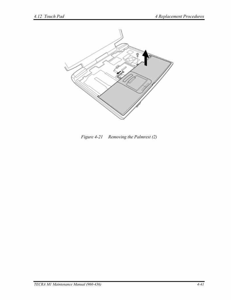
4.12 Touch Pad 4 Replacement Procedures
Figure 4-21 Removing the Palmrest (2)
TECRA M1 Maintenance Manual (960-436) 4-41
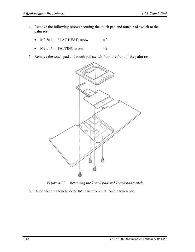
4 Replacement Procedures 4.12 Touch Pad
4. Remove the following screws securing the touch pad and touch pad switch to the palm rest.
• M2.5×4 FLAT HEAD screw ×2
• M2.5×4 TAPPING screw ×2
5. Remove the touch pad and touch pad switch from the front of the palm rest.
Figure 4-22 Removing the Touch pad and Touch pad switch
6. Disconnect the touch pad SUMI card from CN1 on the touch pad.
4-42 TECRA M1 Maintenance Manual (960-436)
4.12 Touch Pad 4 Replacement Procedures
Installing the Touch Pad
To install the touch pad, follow the steps below and refer to figures 4-20 to 4-22.
1. Connect the touch pad SUMI card to CN1 on the touch pad.
2. Install the touch pad and touch pad switches on the palm rest and pass the touch pad SUMI card into the hole of the palm rest. Secure them with the following screws.
• M2.5×4 FLAT HEAD screw ×2
• M2.5×4 TAPPING screw ×2
3. Place the palm rest on the display assembly and secure the latches by pressing it. Secure the palm rest with the following screw.
• M2.5×4 FLAT HEAD screw ×1
4. Connect the touch pad SUMI card to PJ2003 on the system board.
5. Close the display panel and turn the computer face down. Secure the palm rest with the following screws to the display assembly.
• M2.5×4 FLAT HEAD screw ×2
• M2.5×6 FLAT HEAD screw ×3
• M2.5×10 FLAT HEAD screw ×2
• M2.5×16 FLAT HEAD screw ×2
TECRA M1 Maintenance Manual (960-436) 4-43
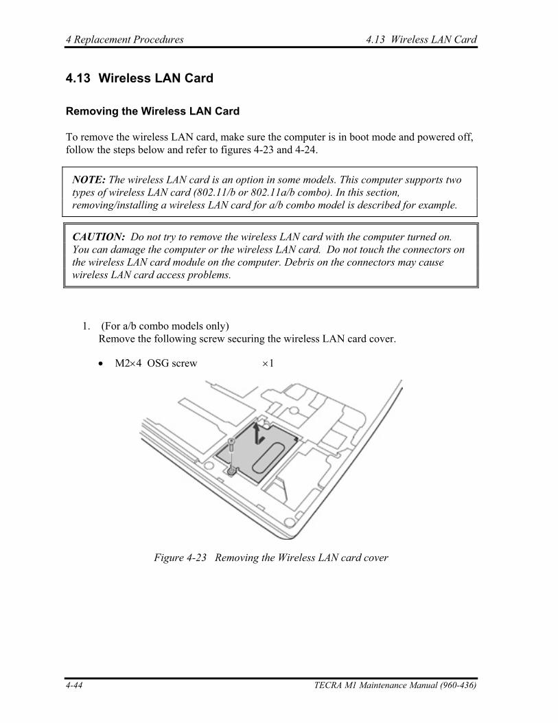
4 Replacement Procedures 4.13 Wireless LAN Card
4.13 Wireless LAN Card
Removing the Wireless LAN Card
To remove the wireless LAN card, make sure the computer is in boot mode and powered off, follow the steps below and refer to figures 4-23 and 4-24.
NOTE: The wireless LAN card is an option in some models. This computer supports two types of wireless LAN card (802.11/b or 802.11a/b combo). In this section, removing/installing a wireless LAN card for a/b combo model is described for example.
CAUTION: Do not try to remove the wireless LAN card with the computer turned on. You can damage the computer or the wireless LAN card. Do not touch the connectors on the wireless LAN card module on the computer. Debris on the connectors may cause wireless LAN card access problems.
1. (For a/b combo models only) Remove the following screw securing the wireless LAN card cover.
• M2×4 OSG screw ×1
Figure 4-23 Removing the Wireless LAN card cover
4-44 TECRA M1 Maintenance Manual (960-436)
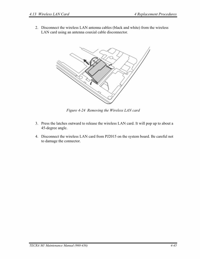
4.13 Wireless LAN Card 4 Replacement Procedures
2. Disconnect the wireless LAN antenna cables (black and white) from the wireless LAN card using an antenna coaxial cable disconnector.
Figure 4-24 Removing the Wireless LAN card
3. Press the latches outward to release the wireless LAN card. It will pop up to about a 45-degree angle.
4. Disconnect the wireless LAN card from PJ2015 on the system board. Be careful not to damage the connector.
TECRA M1 Maintenance Manual (960-436) 4-45
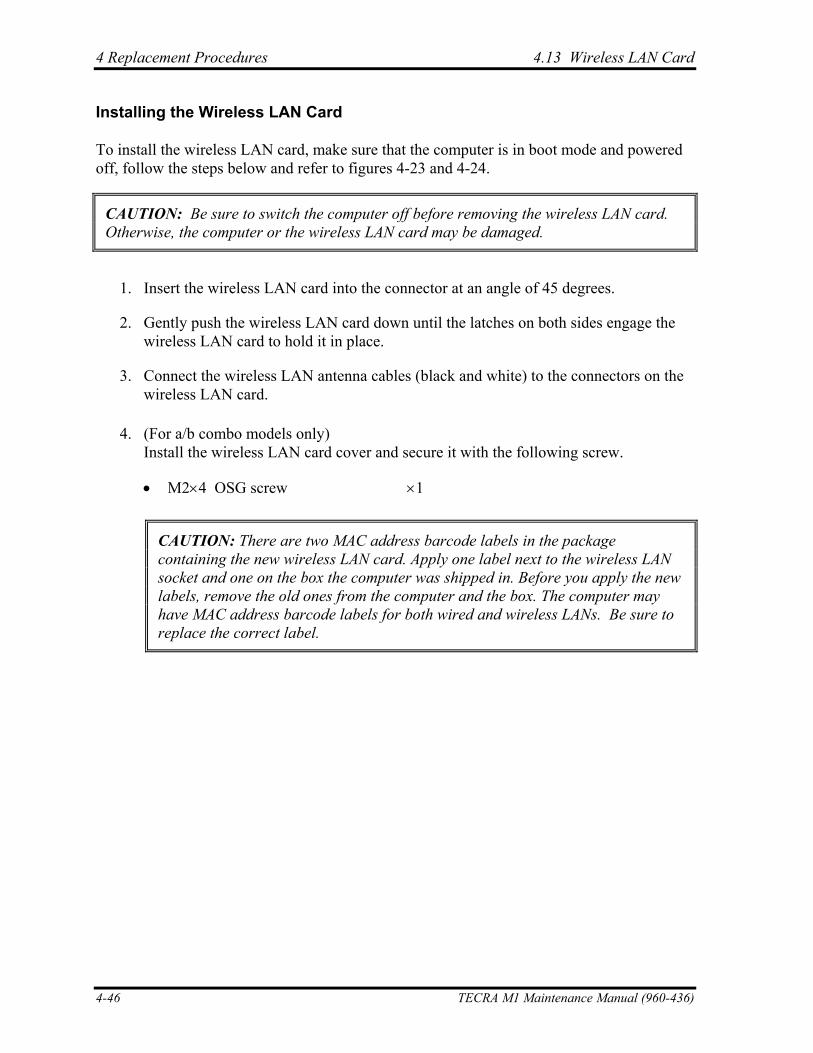
4 Replacement Procedures 4.13 Wireless LAN Card
Installing the Wireless LAN Card
To install the wireless LAN card, make sure that the computer is in boot mode and powered off, follow the steps below and refer to figures 4-23 and 4-24.
CAUTION: Be sure to switch the computer off before removing the wireless LAN card. Otherwise, the computer or the wireless LAN card may be damaged.
1. Insert the wireless LAN card into the connector at an angle of 45 degrees.
2. Gently push the wireless LAN card down until the latches on both sides engage the wireless LAN card to hold it in place.
3. Connect the wireless LAN antenna cables (black and white) to the connectors on the wireless LAN card.
4. (For a/b combo models only) Install the wireless LAN card cover and secure it with the following screw.
• M2×4 OSG screw ×1
CAUTION: There are two MAC address barcode labels in the package containing the new wireless LAN card. Apply one label next to the wireless LAN socket and one on the box the computer was shipped in. Before you apply the new labels, remove the old ones from the computer and the box. The computer may have MAC address barcode labels for both wired and wireless LANs. Be sure to replace the correct label.
4-46 TECRA M1 Maintenance Manual (960-436)
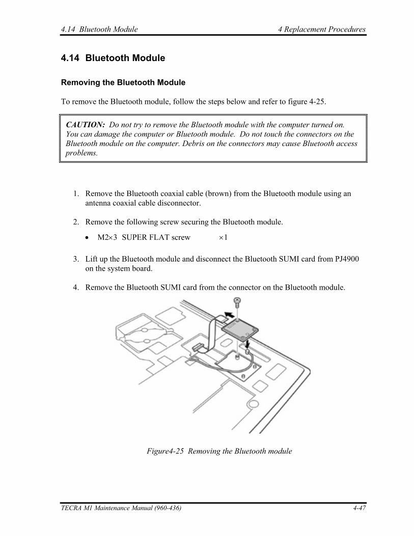
4.14 Bluetooth Module 4 Replacement Procedures
4.14 Bluetooth Module
Removing the Bluetooth Module
To remove the Bluetooth module, follow the steps below and refer to figure 4-25.
CAUTION: Do not try to remove the Bluetooth module with the computer turned on. You can damage the computer or Bluetooth module. Do not touch the connectors on the Bluetooth module on the computer. Debris on the connectors may cause Bluetooth access problems.
1. Remove the Bluetooth coaxial cable (brown) from the Bluetooth module using an antenna coaxial cable disconnector.
2. Remove the following screw securing the Bluetooth module.
• M2×3 SUPER FLAT screw ×1
3. Lift up the Bluetooth module and disconnect the Bluetooth SUMI card from PJ4900 on the system board.
4. Remove the Bluetooth SUMI card from the connector on the Bluetooth module.
Figure4-25 Removing the Bluetooth module
TECRA M1 Maintenance Manual (960-436) 4-47
4 Replacement Procedures 4.14 Bluetooth Module
Installing the Bluetooth Module
To install the Bluetooth module, follow the steps below and refer to figure 4-25.
1. Connect the Bluetooth SUMI card to the connector on the Bluetooth module.
2. Connect the Bluetooth SUMI card to PJ4900 on the system board.
3. Place the Bluetooth module.
4. Secure the Bluetooth module with the following screw.
• M2×3 SUPER FLAT screw ×1
5. Connect the Bluetooth coaxial cable (brown) to the Bluetooth module.
4-48 TECRA M1 Maintenance Manual (960-436)
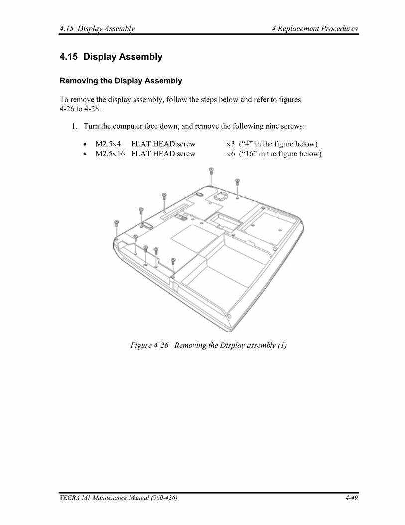
4.15 Display Assembly 4 Replacement Procedures
4.15 Display Assembly
Removing the Display Assembly
To remove the display assembly, follow the steps below and refer to figures 4-26 to 4-28.
1. Turn the computer face down, and remove the following nine screws:
• M2.5×4 FLAT HEAD screw ×3 (“4” in the figure below) • M2.5×16 FLAT HEAD screw ×6 (“16” in the figure below)
Figure 4-26 Removing the Display assembly (1)
TECRA M1 Maintenance Manual (960-436) 4-49
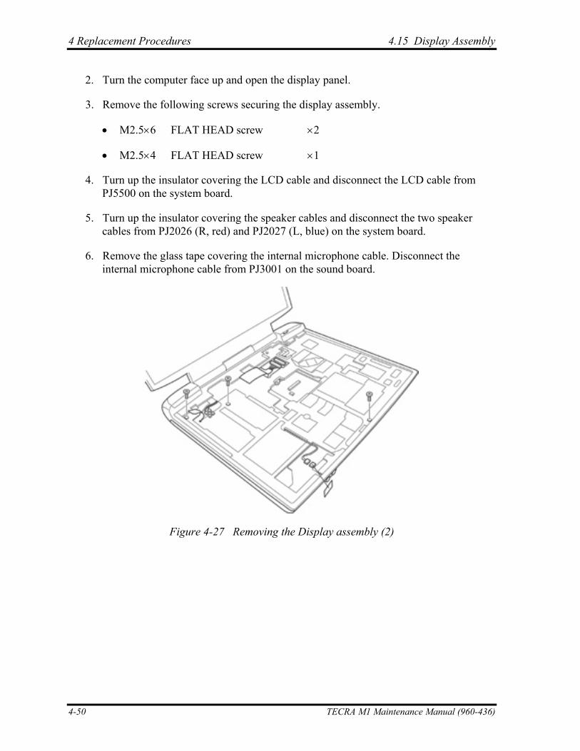
4 Replacement Procedures 4.15 Display Assembly
2. Turn the computer face up and open the display panel.
3. Remove the following screws securing the display assembly.
• M2.5×6 FLAT HEAD screw ×2
• M2.5×4 FLAT HEAD screw ×1
4. Turn up the insulator covering the LCD cable and disconnect the LCD cable from PJ5500 on the system board.
5. Turn up the insulator covering the speaker cables and disconnect the two speaker cables from PJ2026 (R, red) and PJ2027 (L, blue) on the system board.
6. Remove the glass tape covering the internal microphone cable. Disconnect the internal microphone cable from PJ3001 on the sound board.
Figure 4-27 Removing the Display assembly (2)
4-50 TECRA M1 Maintenance Manual (960-436)
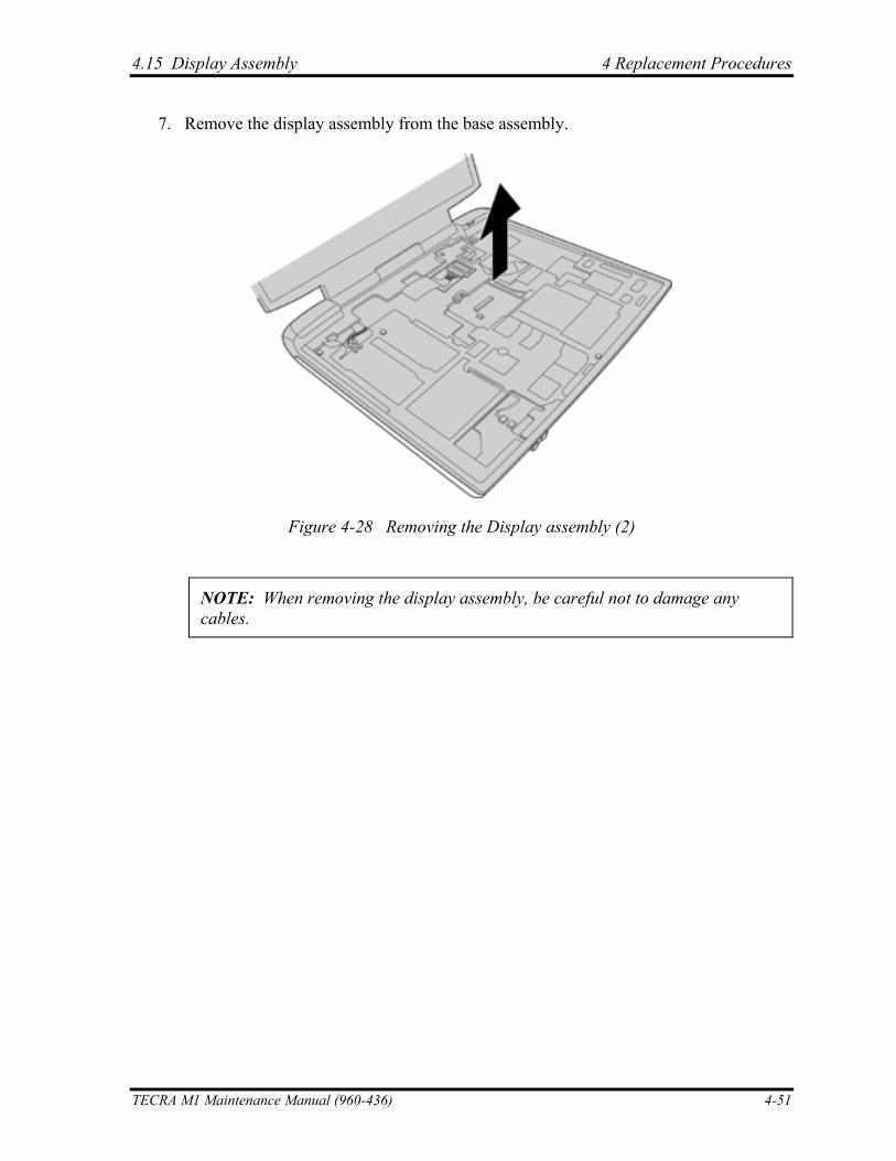
4.15 Display Assembly 4 Replacement Procedures
7. Remove the display assembly from the base assembly.
Figure 4-28 Removing the Display assembly (2)
NOTE: When removing the display assembly, be careful not to damage any cables.
TECRA M1 Maintenance Manual (960-436) 4-51
4 Replacement Procedures 4.15 Display Assembly
Installing the Display Assembly
To install the display assembly, follow the steps below and refer to figures 4-26 and 4-28.
1. Install the display assembly on the base assembly.
NOTE: When installing the display assembly, be careful not to pinch or damage any cables.
2. Press along the edges of the display assembly to secure the latches.
3. Connect the internal microphone cable to PJ3001 on the sound board and stick the glass tape on it.
4. Turn up the insulator and connect the LCD cable to PJ5500 on the system board.
5. Turn up the insulator and connect the two speaker cables to PJ2026 (R, red) and PJ2027 (L, blue) on the system board.
6. Secure the display assembly with the following screws.
• M2.5×6 FLAT HEAD screw ×2
• M2.5×4 FLAT HEAD screw ×1
7. Turn the computer face down and secure the display assembly with the following nine screws:
• M2.5×4 FLAT HEAD screw ×3
• M2.5×16 FLAT HEAD screw ×6
4-52 TECRA M1 Maintenance Manual (960-436)
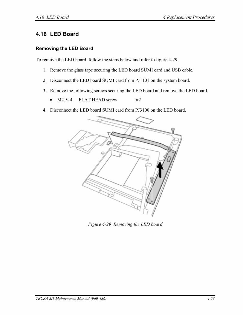
4.16 LED Board 4 Replacement Procedures
4.16 LED Board
Removing the LED Board
To remove the LED board, follow the steps below and refer to figure 4-29.
1. Remove the glass tape securing the LED board SUMI card and USB cable.
2. Disconnect the LED board SUMI card from PJ1101 on the system board.
3. Remove the following screws securing the LED board and remove the LED board.
• M2.5×4 FLAT HEAD screw ×2
4. Disconnect the LED board SUMI card from PJ3100 on the LED board.
Figure 4-29 Removing the LED board
TECRA M1 Maintenance Manual (960-436) 4-53
4 Replacement Procedures 4.16 LED Board
Installing the LED Board
To install the LED board, follow the steps below and refer to figure 4-29.
1. Connect the LED board SUMI card to PJ3100 on the LED board.
2. Place the LED board and secure it with the following screws.
• M2.5×4 FLAT HEAD screws ×2
3. Connect the LED board SUMI card to PJ1101 on the system board.
4. Stick the glass tape to secure the LED board SUMI card and USB cable.
4-54 TECRA M1 Maintenance Manual (960-436)
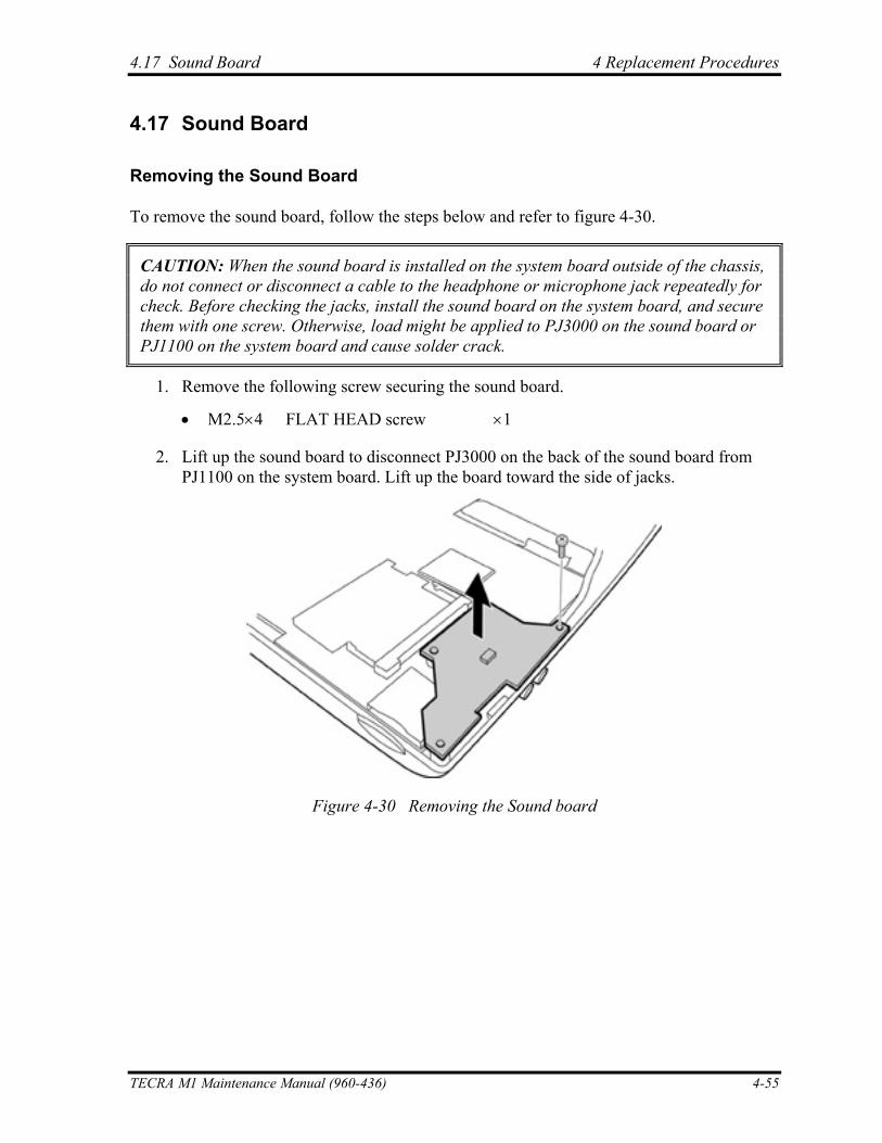
4.17 Sound Board 4 Replacement Procedures
4.17 Sound Board
Removing the Sound Board
To remove the sound board, follow the steps below and refer to figure 4-30.
CAUTION: When the sound board is installed on the system board outside of the chassis, do not connect or disconnect a cable to the headphone or microphone jack repeatedly for check. Before checking the jacks, install the sound board on the system board, and secure them with one screw. Otherwise, load might be applied to PJ3000 on the sound board or PJ1100 on the system board and cause solder crack.
1. Remove the following screw securing the sound board.
• M2.5×4 FLAT HEAD screw ×1
2. Lift up the sound board to disconnect PJ3000 on the back of the sound board from PJ1100 on the system board. Lift up the board toward the side of jacks.
Figure 4-30 Removing the Sound board
TECRA M1 Maintenance Manual (960-436) 4-55
4 Replacement Procedures 4.17 Sound Board
Installing the Sound Board
To install the sound board, follow the steps below and refer to figure 4-30.
1. Install the sound board and press it to connect PJ3000 on the back of the sound board to PJ1100 on the system board. When installing the sound board, insert the two jacks and a volume controller into the hole of the chassis first.
2. Secure the sound board with the following screw.
• M2.5×4 FLAT HEAD screw ×1
4-56 TECRA M1 Maintenance Manual (960-436)
4.18 System Board/RTC Battery/DC-IN Jack 4 Replacement Procedures
4.18 System Board/RTC Battery/DC-IN Jack
WARNING: When replacing the RTC battery, be sure to use genuine batteries or replacement batteries authorized by Toshiba. Installing the wrong battery could cause a battery explosion or other damage.
If the RTC battery is found abnormal, it must not be installed. Replace it with a new battery, and dispose of the old one according to the local regulations.
Check for any of the following signs of damage:
1) Electrolyte leakage
• Corrosion (greenish color) on the battery connector or cable
• Corrosion on the computer's battery connector
• White powder on any part of the battery
• White powder in the battery tray
• Clear liquid on the battery
• Clear liquid in the battery tray
• Clear liquid on any board near the battery
2) Damage to the connection cable
3) Damage to the connector housing
If any powder or liquid is found in or around the battery tray, clean it. Be careful not to let any leaked material contact your eyes or mouth. Do not inhale fumes from leaked material. If leaked material contacts your skin, eyes or mouth, wash the affected area thoroughly with clean water.
TECRA M1 Maintenance Manual (960-436) 4-57
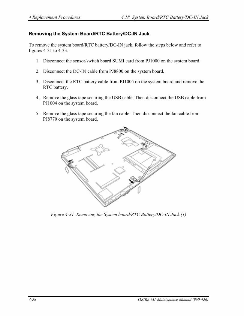
4 Replacement Procedures 4.18 System Board/RTC Battery/DC-IN Jack
Removing the System Board/RTC Battery/DC-IN Jack
To remove the system board/RTC battery/DC-IN jack, follow the steps below and refer to figures 4-31 to 4-33.
1. Disconnect the sensor/switch board SUMI card from PJ1000 on the system board.
2. Disconnect the DC-IN cable from PJ8800 on the system board.
3. Disconnect the RTC battery cable from PJ1005 on the system board and remove the RTC battery.
4. Remove the glass tape securing the USB cable. Then disconnect the USB cable from PJ1004 on the system board.
5. Remove the glass tape securing the fan cable. Then disconnect the fan cable from PJ8770 on the system board.
Figure 4-31 Removing the System board/RTC Battery/DC-IN Jack (1)
4-58 TECRA M1 Maintenance Manual (960-436)
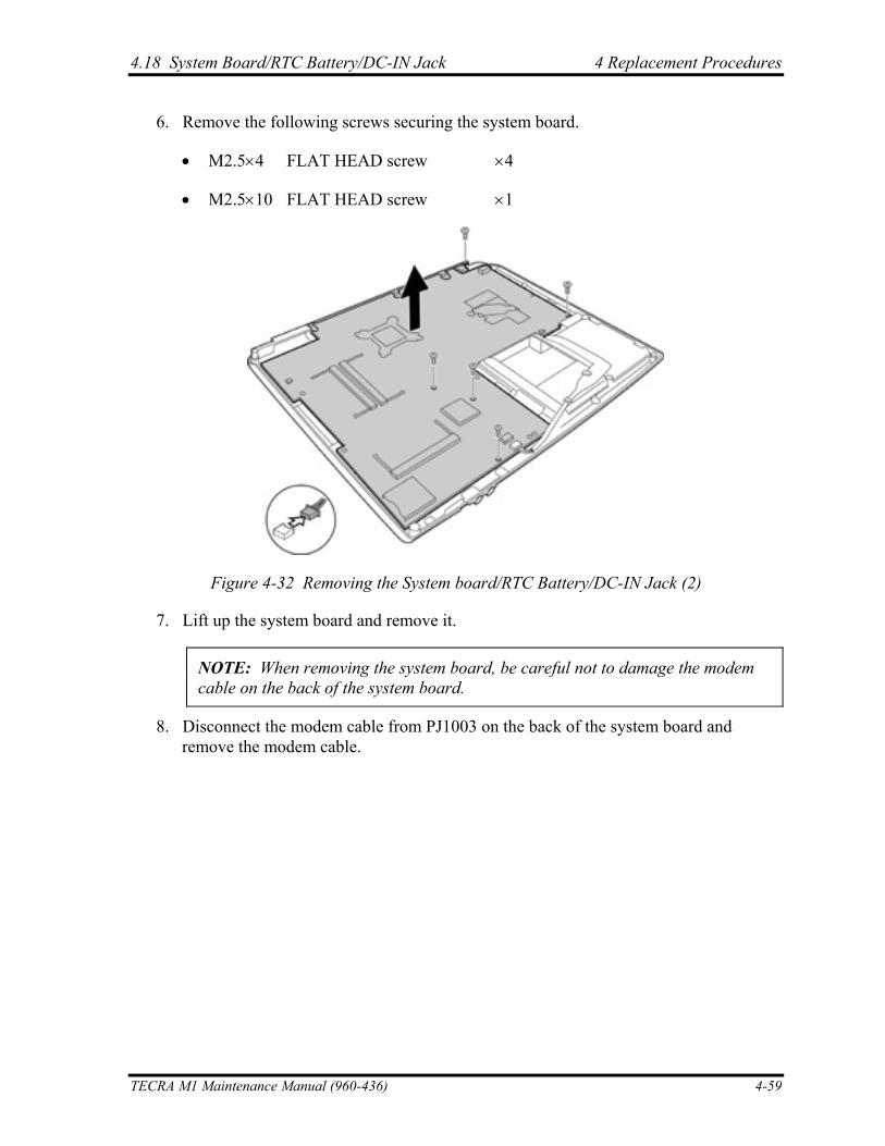
4.18 System Board/RTC Battery/DC-IN Jack 4 Replacement Procedures
6. Remove the following screws securing the system board.
• M2.5×4 FLAT HEAD screw ×4
• M2.5×10 FLAT HEAD screw ×1
Figure 4-32 Removing the System board/RTC Battery/DC-IN Jack (2)
7. Lift up the system board and remove it.
NOTE: When removing the system board, be careful not to damage the modem cable on the back of the system board.
8. Disconnect the modem cable from PJ1003 on the back of the system board and remove the modem cable.
TECRA M1 Maintenance Manual (960-436) 4-59
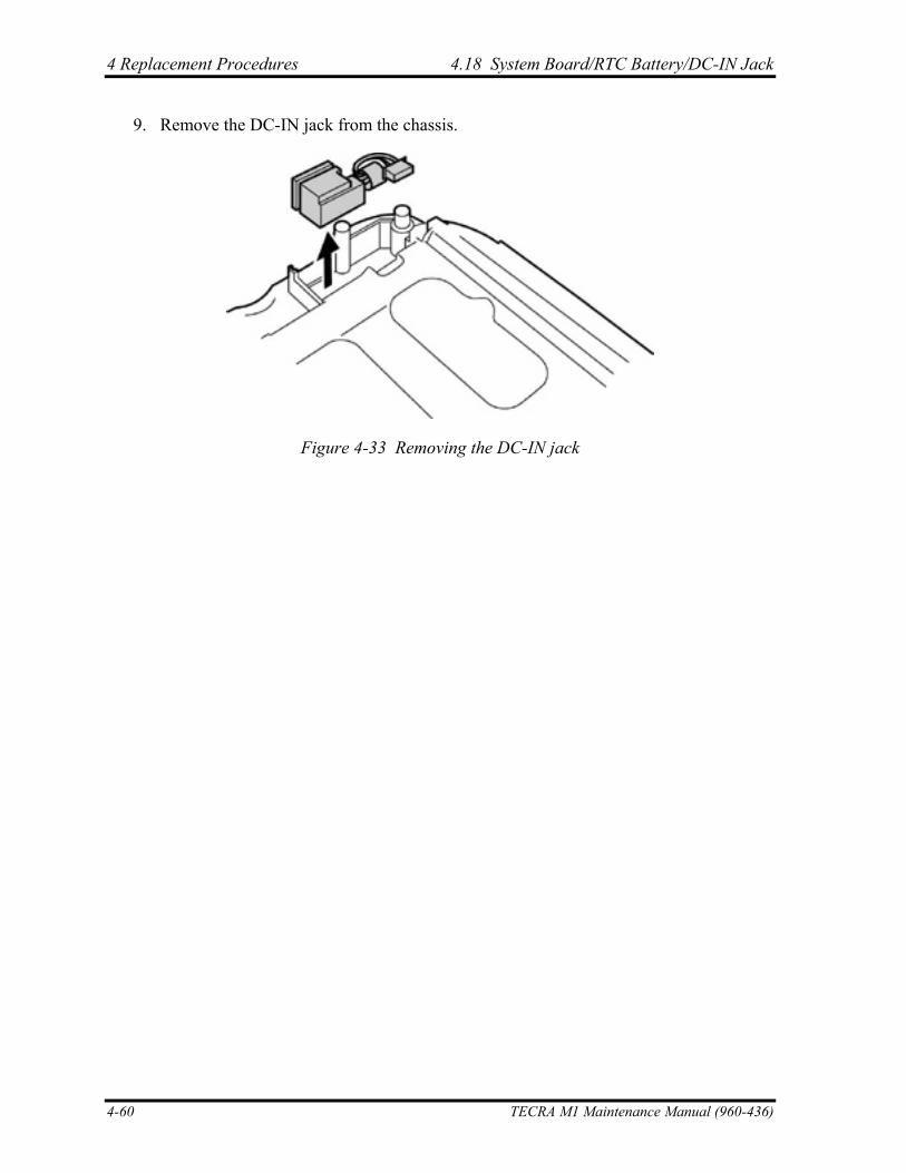
4 Replacement Procedures 4.18 System Board/RTC Battery/DC-IN Jack
9. Remove the DC-IN jack from the chassis.
Figure 4-33 Removing the DC-IN jack
4-60 TECRA M1 Maintenance Manual (960-436)
4.18 System Board/RTC Battery/DC-IN Jack 4 Replacement Procedures
TECRA M1 Maintenance Manual (960-436) 4-61
Installing the System Board/RTC Battery/DC-IN Jack
To install the system board/RTC battery/DC-IN jack, follow the steps below and refer to figures 4-31 to 4-33.
1. Install the DC-IN jack on the chassis.
2. Connect the modem cable to PJ1003 on the back of the system board and pass the cable under the insulator on the side of the CPU.
3. Install the system board. Pass the modem cable toward back through the hole for the CPU of the chassis. Set the cable into the hole of the insulator for modem daughter card.
NOTE: When installing the system board, be careful not to pinch or damage the USB cable, DC-IN cable, modem cable or RTC battery cable.
4. Secure the system board with the following screws.
• M2.5×4 FLAT HEAD screw ×4
• M2.5×10 FLAT HEAD screw ×1
5. Connect the fan cable to PJ8770 on the system board. Then stick the glass tape to secure the fan cable.
6. Connect the USB cable to PJ1004 on the system board. Then stick the glass tape to secure the USB cable.
7. Connect the RTC battery cable to PJ1005 on the system board. Install the RTC battery vertically into the empty space between the system board and chassis.
8. Connect the DC-IN cable to PJ8800 on the system board.
9. Connect the sensor/switch board SUMI card to PJ1000 on the system board.
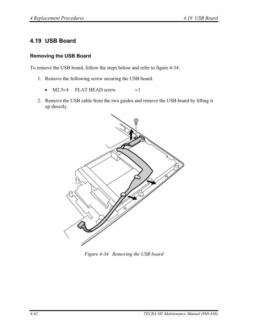
4 Replacement Procedures 4.19 USB Board
4 Replacement Procedures
4.19 USB Board
Removing the USB Board
To remove the USB board, follow the steps below and refer to figure 4-34.
1. Remove the following screw securing the USB board.
• M2.5×4 FLAT HEAD screw ×1
2. Remove the USB cable from the two guides and remove the USB board by lifting it up directly.
Figure 4-34 Removing the USB board
4-62 TECRA M1 Maintenance Manual (960-436)
4.19 USB Board 4 Replacement Procedures
Installing the USB Board
To install the USB board, follow the steps below and refer to the figure 4-34.
1. Fit the USB cable to the two guides and install the USB board with its hole attached to the boss of the chassis.
2. Secure the USB board with the following screw.
• M2.5×4 FLAT HEAD screw ×1
TECRA M1 Maintenance Manual (960-436) 4-63
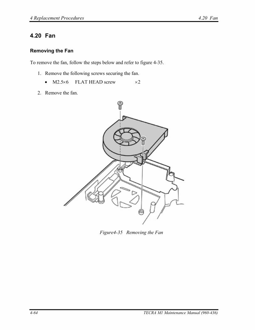
4 Replacement Procedures 4.20 Fan
4.20 Fan
Removing the Fan
To remove the fan, follow the steps below and refer to figure 4-35.
1. Remove the following screws securing the fan.
• M2.5×6 FLAT HEAD screw ×2
2. Remove the fan.
Figure4-35 Removing the Fan
4-64 TECRA M1 Maintenance Manual (960-436)
4.20 Fan 4 Replacement Procedures
Installing the Fan
To install the fan, follow the steps below and refer to figure 4-35.
1. Place the fan.
2. Secure the fan with the following screws.
• M2.5×6 FLAT HEAD screw ×2
TECRA M1 Maintenance Manual (960-436) 4-65
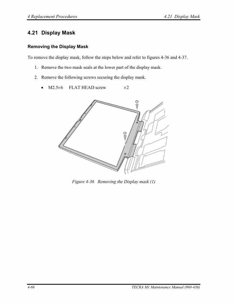
4 Replacement Procedures 4.21 Display Mask
4.21 Display Mask
Removing the Display Mask
To remove the display mask, follow the steps below and refer to figures 4-36 and 4-37.
1. Remove the two mask seals at the lower part of the display mask.
2. Remove the following screws securing the display mask.
• M2.5×6 FLAT HEAD screw ×2
Figure 4-36 Removing the Display mask (1)
4-66 TECRA M1 Maintenance Manual (960-436)
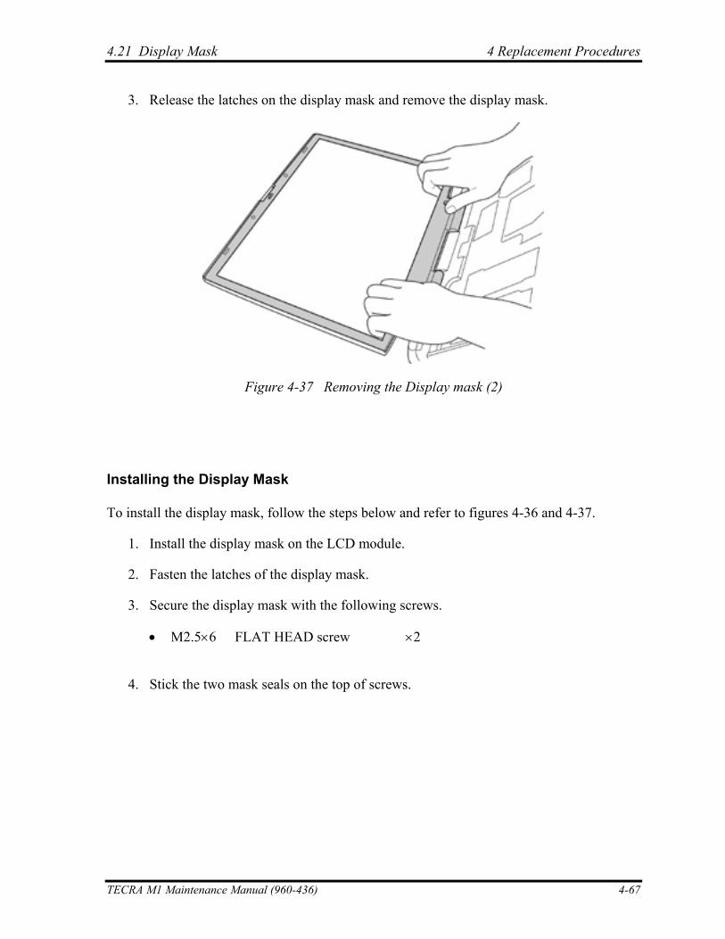
4.21 Display Mask 4 Replacement Procedures
3. Release the latches on the display mask and remove the display mask.
Figure 4-37 Removing the Display mask (2)
Installing the Display Mask
To install the display mask, follow the steps below and refer to figures 4-36 and 4-37.
1. Install the display mask on the LCD module.
2. Fasten the latches of the display mask.
3. Secure the display mask with the following screws.
• M2.5×6 FLAT HEAD screw ×2
4. Stick the two mask seals on the top of screws.
TECRA M1 Maintenance Manual (960-436) 4-67
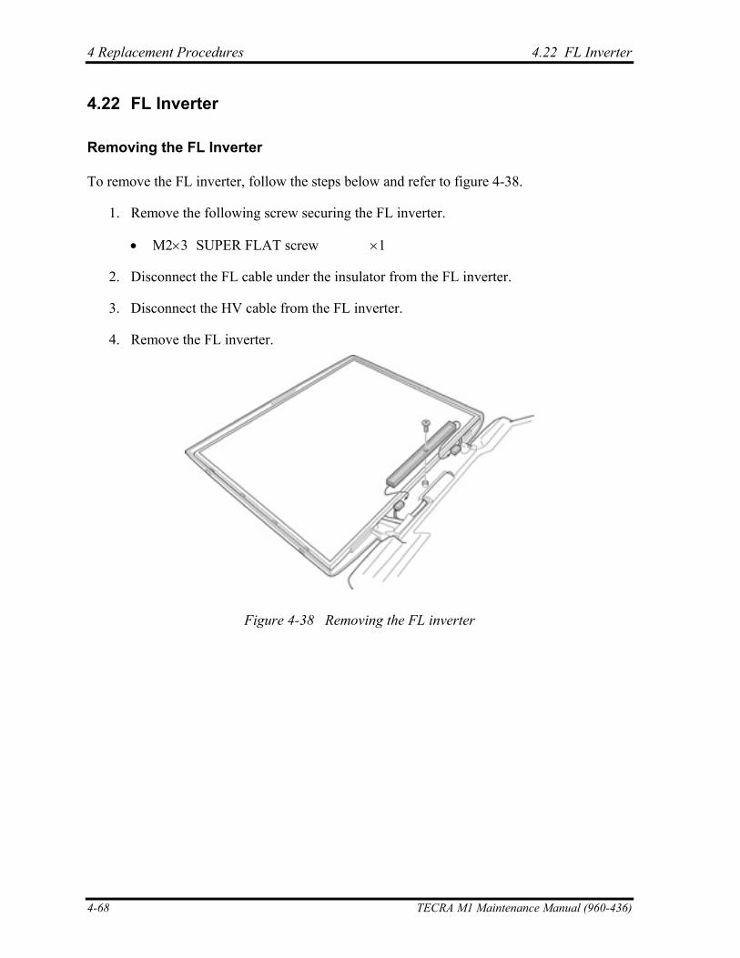
4 Replacement Procedures 4.22 FL Inverter
4.22 FL Inverter
Removing the FL Inverter
To remove the FL inverter, follow the steps below and refer to figure 4-38.
1. Remove the following screw securing the FL inverter.
• M2×3 SUPER FLAT screw ×1
2. Disconnect the FL cable under the insulator from the FL inverter.
3. Disconnect the HV cable from the FL inverter.
4. Remove the FL inverter.
Figure 4-38 Removing the FL inverter
4-68 TECRA M1 Maintenance Manual (960-436)
4.22 FL Inverter 4 Replacement Procedures
Installing the FL Inverter
To install the FL inverter, follow the steps below and refer to figure 4-38.
1. Connect the FL cable and the HV cable to the FL inverter.
2. Seat the FL inverter and stick the insulator on the FL inverter of the FL cable side.
3. Secure the FL inverter with the following screw.
• M2×3 SUPER FLAT screw ×1
TECRA M1 Maintenance Manual (960-436) 4-69
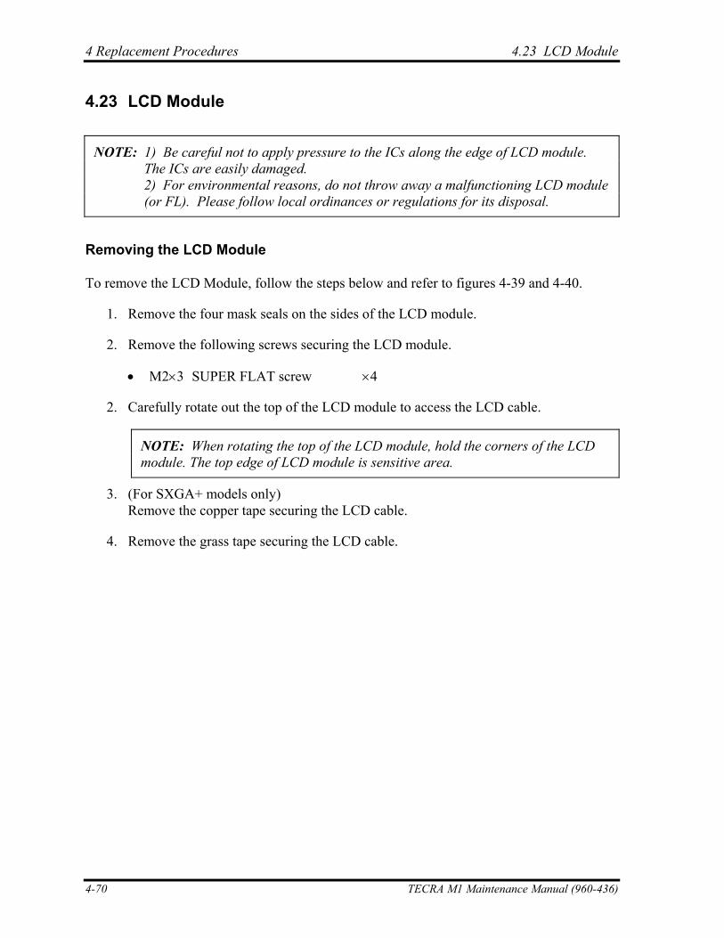
4 Replacement Procedures 4.23 LCD Module
4.23 LCD Module
NOTE: 1) Be careful not to apply pressure to the ICs along the edge of LCD module. The ICs are easily damaged. 2) For environmental reasons, do not throw away a malfunctioning LCD module (or FL). Please follow local ordinances or regulations for its disposal.
Removing the LCD Module
To remove the LCD Module, follow the steps below and refer to figures 4-39 and 4-40.
1. Remove the four mask seals on the sides of the LCD module.
2. Remove the following screws securing the LCD module.
• M2×3 SUPER FLAT screw ×4
2. Carefully rotate out the top of the LCD module to access the LCD cable.
NOTE: When rotating the top of the LCD module, hold the corners of the LCD module. The top edge of LCD module is sensitive area.
3. (For SXGA+ models only) Remove the copper tape securing the LCD cable.
4. Remove the grass tape securing the LCD cable.
4-70 TECRA M1 Maintenance Manual (960-436)
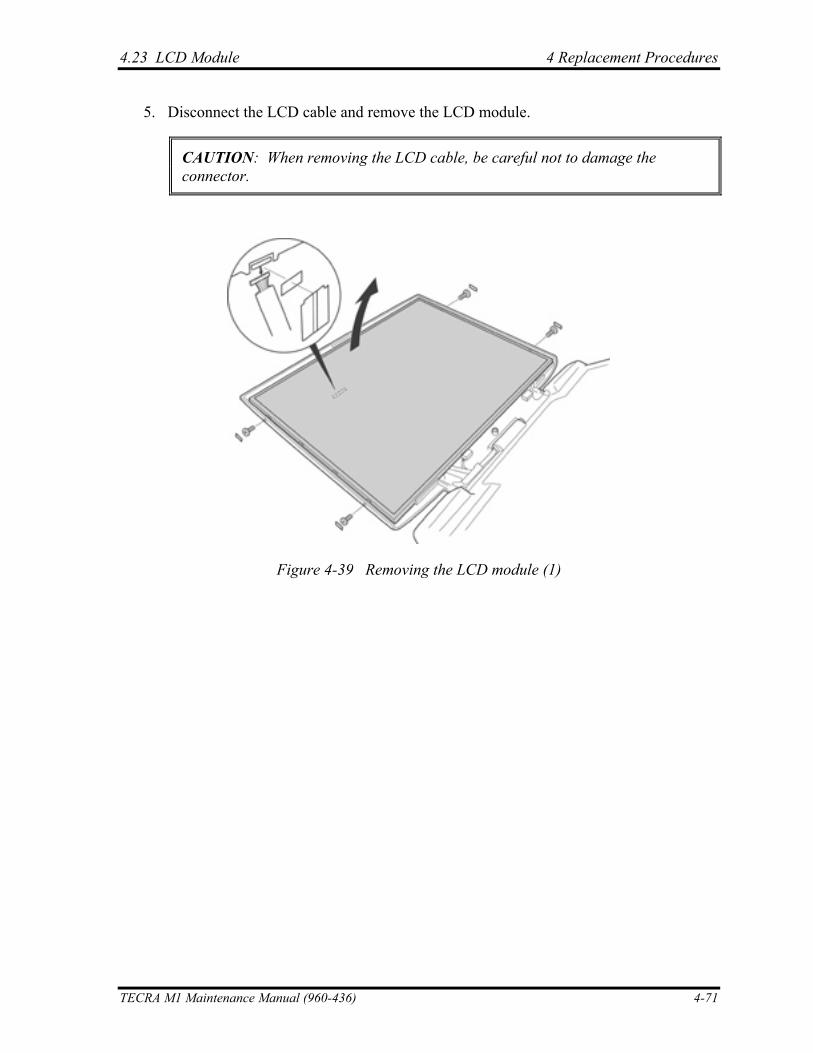
4.23 LCD Module 4 Replacement Procedures
5. Disconnect the LCD cable and remove the LCD module.
CAUTION: When removing the LCD cable, be careful not to damage the connector.
Figure 4-39 Removing the LCD module (1)
TECRA M1 Maintenance Manual (960-436) 4-71
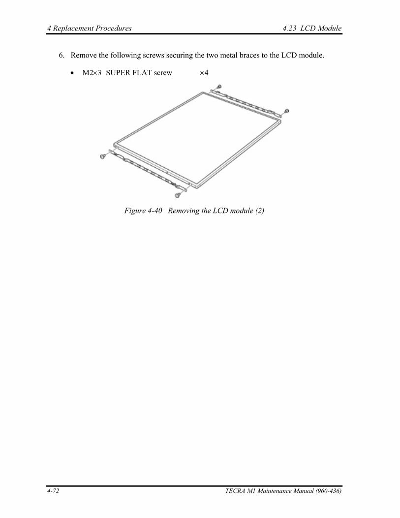
4 Replacement Procedures 4.23 LCD Module
6. Remove the following screws securing the two metal braces to the LCD module.
• M2×3 SUPER FLAT screw ×4
Figure 4-40 Removing the LCD module (2)
4-72 TECRA M1 Maintenance Manual (960-436)
4.23 LCD Module 4 Replacement Procedures
Installing the LCD Module
To install the LCD module, follow the steps below and refer to figures 4-39 and 4-40.
1. Secure the two metal braces to the LCD module with the following screws.
• M2×3 SUPER FLAT screw ×4
2. Lean the LCD module against the lower side of the display cover.
3. Connect the LCD cable to the connector on the back of the LCD module. Stick the glass tape on the LCD cable.
4. (For SXGA+ models only) Stick the copper tape on the LCD cable and glass tape. Make sure the copper tape covers the connector on the display cover and the LCD cable.
5. Seat the LCD module and secure it with the following screws.
• M2×3 SUPER FLAT screw ×4
6. Stick the four mask seals on the sides of the LCD module.
TECRA M1 Maintenance Manual (960-436) 4-73
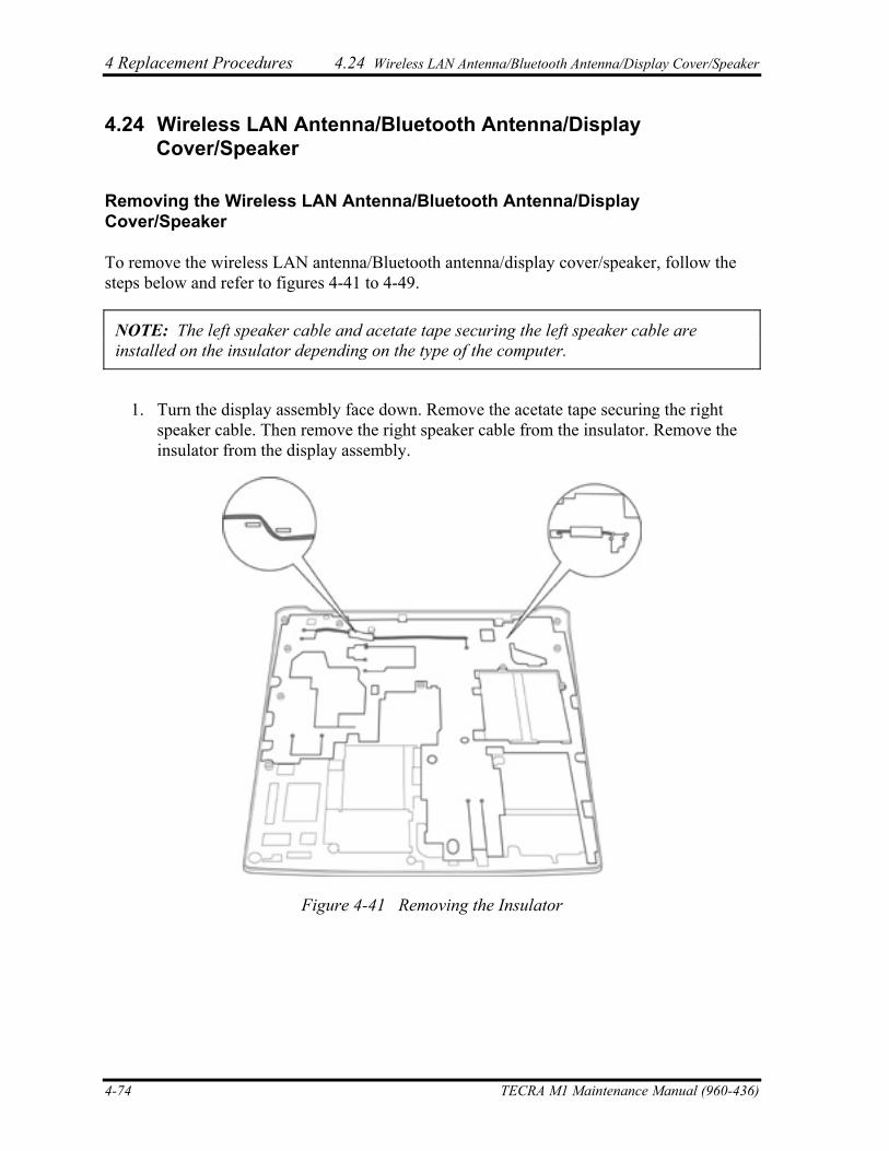
4 Replacement Procedures 4.24 Wireless LAN Antenna/Bluetooth Antenna/Display Cover/Speaker
4.24 Wireless LAN Antenna/Bluetooth Antenna/Display Cover/Speaker
Removing the Wireless LAN Antenna/Bluetooth Antenna/Display Cover/Speaker
To remove the wireless LAN antenna/Bluetooth antenna/display cover/speaker, follow the steps below and refer to figures 4-41 to 4-49.
NOTE: The left speaker cable and acetate tape securing the left speaker cable are installed on the insulator depending on the type of the computer.
1. Turn the display assembly face down. Remove the acetate tape securing the right
speaker cable. Then remove the right speaker cable from the insulator. Remove the insulator from the display assembly.
Figure 4-41 Removing the Insulator
4-74 TECRA M1 Maintenance Manual (960-436)
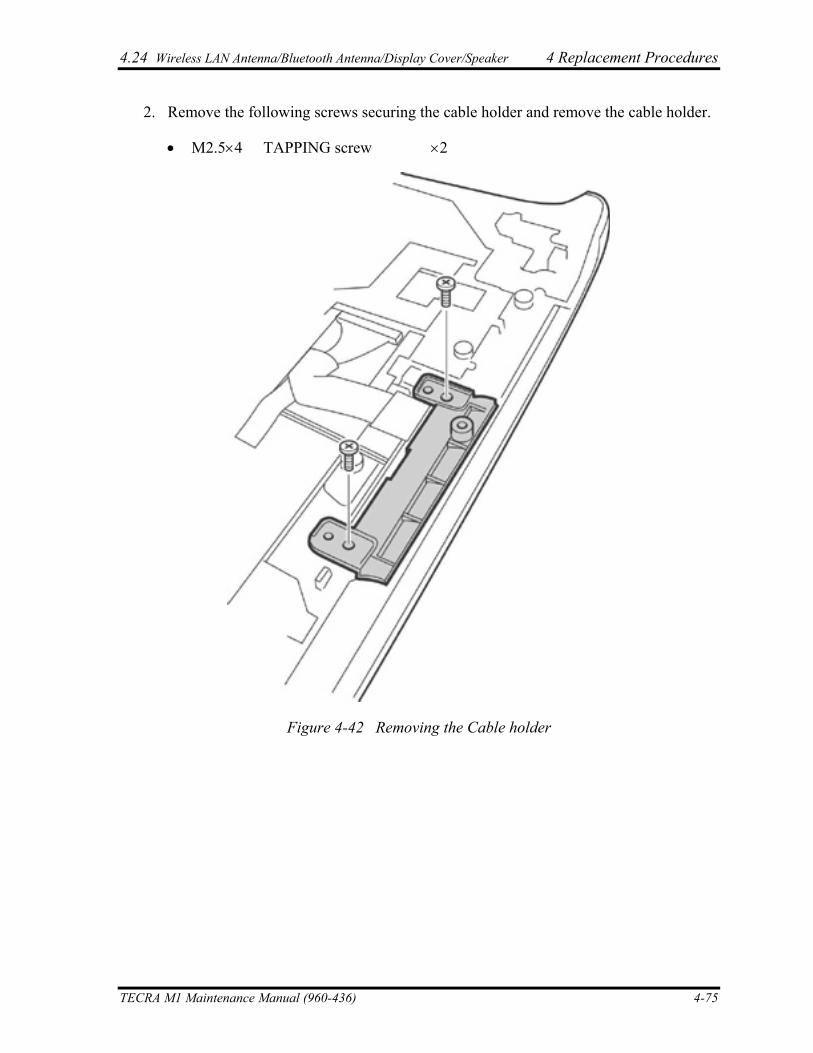
4.24 Wireless LAN Antenna/Bluetooth Antenna/Display Cover/Speaker 4 Replacement Procedures
2. Remove the following screws securing the cable holder and remove the cable holder.
• M2.5×4 TAPPING screw ×2
Figure 4-42 Removing the Cable holder
TECRA M1 Maintenance Manual (960-436) 4-75
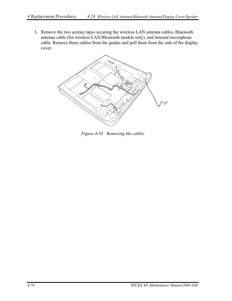
4 Replacement Procedures 4.24 Wireless LAN Antenna/Bluetooth Antenna/Display Cover/Speaker
3. Remove the two acetate tapes securing the wireless LAN antenna cables, Bluetooth antenna cable (for wireless LAN/Bluetooth models only), and internal microphone cable. Remove these cables from the guides and pull them from the side of the display cover.
Figure 4-43 Removing the cables
4-76 TECRA M1 Maintenance Manual (960-436)
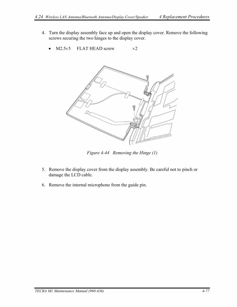
4.24 Wireless LAN Antenna/Bluetooth Antenna/Display Cover/Speaker 4 Replacement Procedures
4. Turn the display assembly face up and open the display cover. Remove the following screws securing the two hinges to the display cover.
• M2.5×5 FLAT HEAD screw ×2
Figure 4-44 Removing the Hinge (1)
5. Remove the display cover from the display assembly. Be careful not to pinch or damage the LCD cable.
6. Remove the internal microphone from the guide pin.
TECRA M1 Maintenance Manual (960-436) 4-77
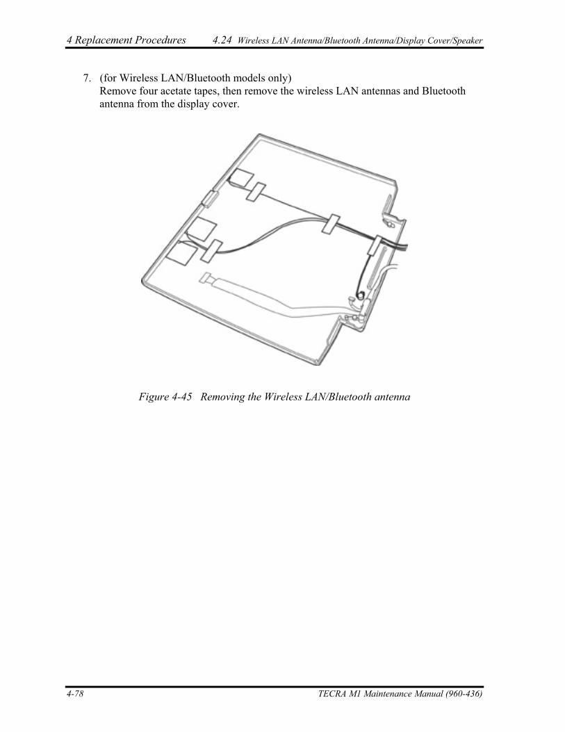
4 Replacement Procedures 4.24 Wireless LAN Antenna/Bluetooth Antenna/Display Cover/Speaker
7. (for Wireless LAN/Bluetooth models only) Remove four acetate tapes, then remove the wireless LAN antennas and Bluetooth antenna from the display cover.
Figure 4-45 Removing the Wireless LAN/Bluetooth antenna
4-78 TECRA M1 Maintenance Manual (960-436)
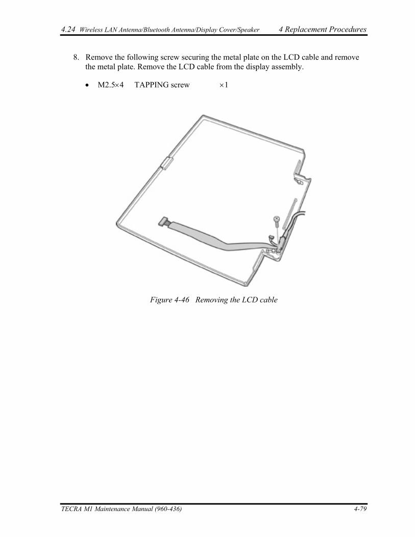
4.24 Wireless LAN Antenna/Bluetooth Antenna/Display Cover/Speaker 4 Replacement Procedures
8. Remove the following screw securing the metal plate on the LCD cable and remove the metal plate. Remove the LCD cable from the display assembly.
• M2.5×4 TAPPING screw ×1
Figure 4-46 Removing the LCD cable
TECRA M1 Maintenance Manual (960-436) 4-79
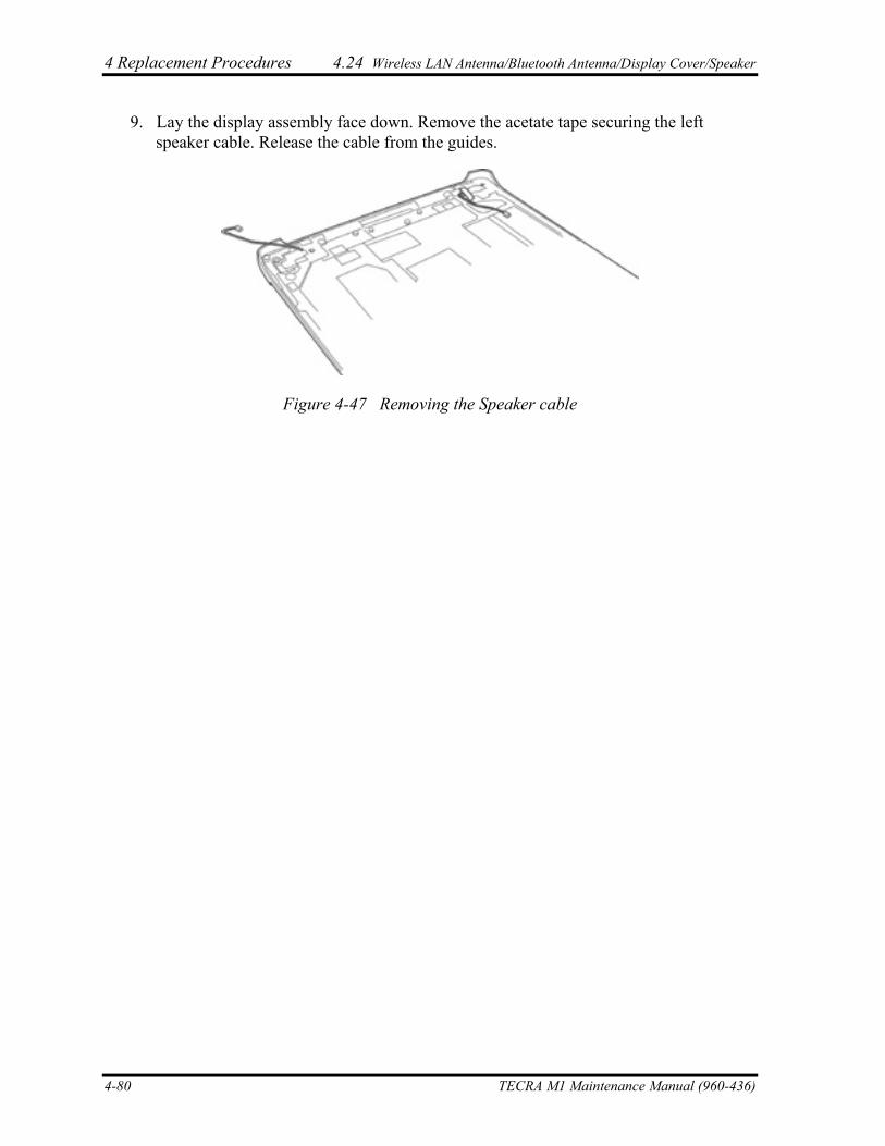
4 Replacement Procedures 4.24 Wireless LAN Antenna/Bluetooth Antenna/Display Cover/Speaker
9. Lay the display assembly face down. Remove the acetate tape securing the left speaker cable. Release the cable from the guides.
Figure 4-47 Removing the Speaker cable
4-80 TECRA M1 Maintenance Manual (960-436)
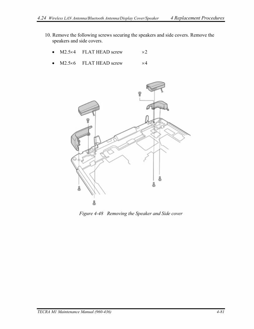
4.24 Wireless LAN Antenna/Bluetooth Antenna/Display Cover/Speaker 4 Replacement Procedures
10. Remove the following screws securing the speakers and side covers. Remove the speakers and side covers.
• M2.5×4 FLAT HEAD screw ×2
• M2.5×6 FLAT HEAD screw ×4
Figure 4-48 Removing the Speaker and Side cover
TECRA M1 Maintenance Manual (960-436) 4-81
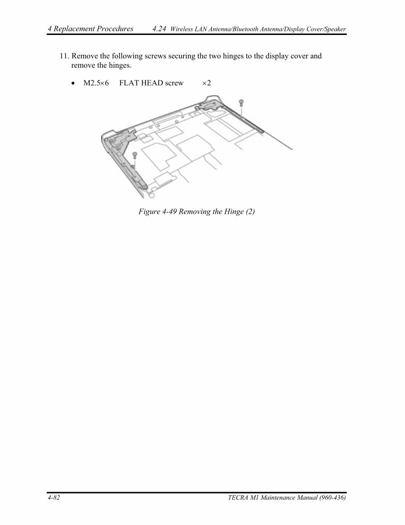
4 Replacement Procedures 4.24 Wireless LAN Antenna/Bluetooth Antenna/Display Cover/Speaker
11. Remove the following screws securing the two hinges to the display cover and remove the hinges.
• M2.5×6 FLAT HEAD screw ×2
Figure 4-49 Removing the Hinge (2)
4-82 TECRA M1 Maintenance Manual (960-436)
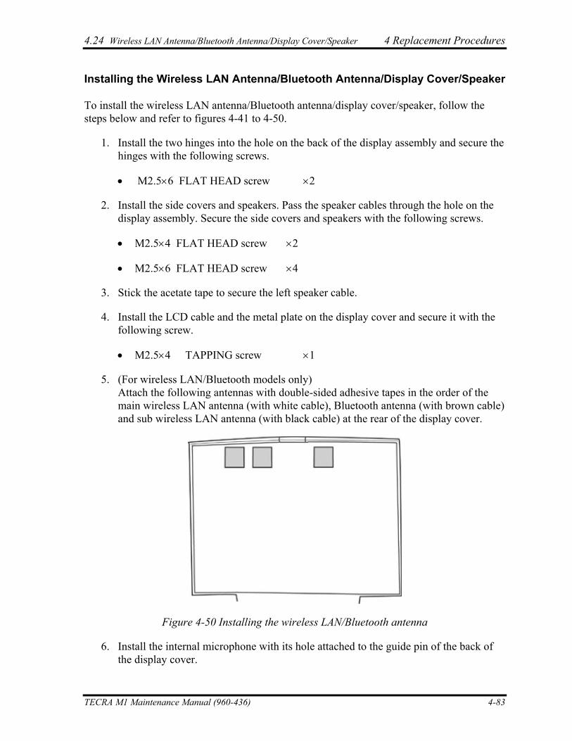
4.24 Wireless LAN Antenna/Bluetooth Antenna/Display Cover/Speaker 4 Replacement Procedures
Installing the Wireless LAN Antenna/Bluetooth Antenna/Display Cover/Speaker
To install the wireless LAN antenna/Bluetooth antenna/display cover/speaker, follow the steps below and refer to figures 4-41 to 4-50.
1. Install the two hinges into the hole on the back of the display assembly and secure the hinges with the following screws.
• M2.5×6 FLAT HEAD screw ×2
2. Install the side covers and speakers. Pass the speaker cables through the hole on the display assembly. Secure the side covers and speakers with the following screws.
• M2.5×4 FLAT HEAD screw ×2
• M2.5×6 FLAT HEAD screw ×4
3. Stick the acetate tape to secure the left speaker cable.
4. Install the LCD cable and the metal plate on the display cover and secure it with the following screw.
• M2.5×4 TAPPING screw ×1
5. (For wireless LAN/Bluetooth models only) Attach the following antennas with double-sided adhesive tapes in the order of the main wireless LAN antenna (with white cable), Bluetooth antenna (with brown cable) and sub wireless LAN antenna (with black cable) at the rear of the display cover.
Figure 4-50 Installing the wireless LAN/Bluetooth antenna
6. Install the internal microphone with its hole attached to the guide pin of the back of the display cover.
TECRA M1 Maintenance Manual (960-436) 4-83
4 Replacement Procedures 4.24 Wireless LAN Antenna/Bluetooth Antenna/Display Cover/Speaker
4-84 TECRA M1 Maintenance Manual (960-436)
7. Install the display cover to the display assembly. Pass the LCD cable through the hole from the front of the display assembly toward the bottom. Secure the two hinges on the display assembly to the display cover with the following screws.
• M2.5×5 FLAT HEAD screw ×2
8. Pass the wireless LAN cables, Bluetooth cable (for wireless LAN/Bluetooth models only) and internal microphone cable through the hole from the front toward the back of the display assembly.
9. Hook the wireless LAN cables, Bluetooth cable (for wireless LAN/Bluetooth models only) and internal microphone cable on the guides on the back of the display assembly. Stick the two acetate tapes on these cables.
10. Install the cable holder on the wireless LAN antenna cables, Bluetooth antenna cable (for wireless LAN/Bluetooth models only), internal microphone cable. Secure the holder with the following screws.
• M2.5×4 TAPPING screw ×2
11. Install the insulator to cover the back of the display assembly. Pass the right speaker cable through the guides of the insulator.
NOTE: The left speaker cable and acetate tape securing the left speaker cable are installed on the insulator depending on the type of the computer.
4.25 Fluorescent Lamp 4 Replacement Procedures
4
4.25 Fluorescent Lamp
This system uses LCD modules from the following suppliers. The procedure for replacing the fluorescent lamp is different for each LCD module. Refer to the appropriate procedure.
Type Part No. Supplier Section
14.1-inch (XGA) VF2092P03 TOSHIBA 4.25.1
14.1-inch (SXGA+) VF2074P01 Sharp 4.25.2
NOTE: - When working with an LCD module, always use a flat, grounded table.
- Handle the backlight unit in the environment without dust, such as on the clean bench. Keep the worktable free from any screws or other material that may scratch the LCD surface.
- Use an anti-static or protective sheet.
- When replacing the FL unit, cover with a finger protector or similar to prevent soiling or scratching the LCD panel.
- Be careful when handling the lamp. Excessive force may break the lamp.
- Be careful not to soil or deform the lamp reflector.
- Make sure that the power of the LCD module is turned off before connecting or disconnecting cables and connectors.
TECRA M1 Maintenance Manual (960-436) 4-85
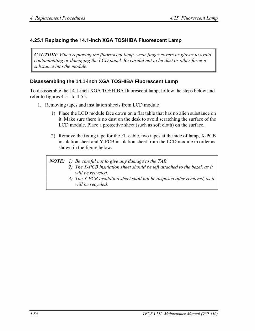
4 Replacement Procedures 4.25 Fluorescent Lamp
4.25.1 Replacing the 14.1-inch XGA TOSHIBA Fluorescent Lamp
CAUTION: When replacing the fluorescent lamp, wear finger covers or gloves to avoid contaminating or damaging the LCD panel. Be careful not to let dust or other foreign substance into the module.
Disassembling the 14.1-inch XGA TOSHIBA Fluorescent Lamp
To disassemble the 14.1-inch XGA TOSHIBA fluorescent lamp, follow the steps below and refer to figures 4-51 to 4-55.
1. Removing tapes and insulation sheets from LCD module
1) Place the LCD module face down on a flat table that has no alien substance on it. Make sure there is no dust on the desk to avoid scratching the surface of the LCD module. Place a protective sheet (such as soft cloth) on the surface.
2) Remove the fixing tape for the FL cable, two tapes at the side of lamp, X-PCB insulation sheet and Y-PCB insulation sheet from the LCD module in order as shown in the figure below.
NOTE: 1) Be careful not to give any damage to the TAB. 2) The X-PCB insulation sheet should be left attached to the bezel, as it will be recycled. 3) The Y-PCB insulation sheet shall not be disposed after removed, as it will be recycled.
4-86 TECRA M1 Maintenance Manual (960-436)
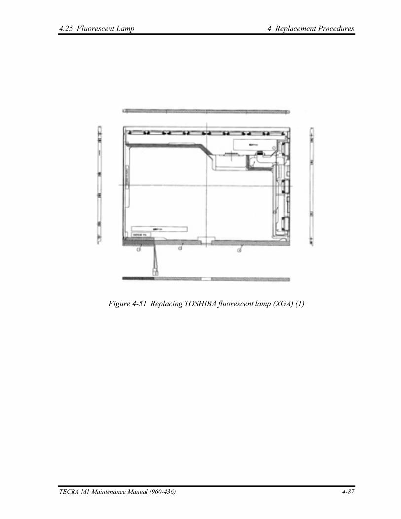
4.25 Fluorescent Lamp 4 Replacement Procedures
Figure 4-51 Replacing TOSHIBA fluorescent lamp (XGA) (1)
TECRA M1 Maintenance Manual (960-436) 4-87
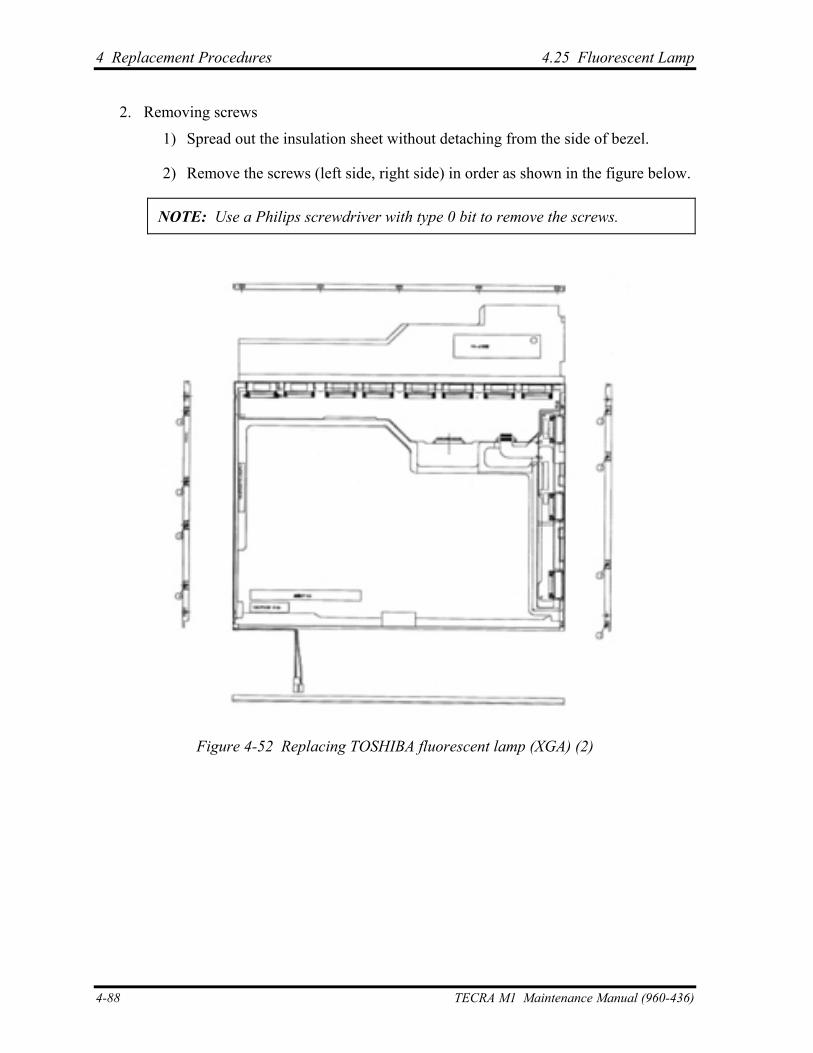
4 Replacement Procedures 4.25 Fluorescent Lamp
2. Removing screws
1) Spread out the insulation sheet without detaching from the side of bezel.
2) Remove the screws (left side, right side) in order as shown in the figure below.
NOTE: Use a Philips screwdriver with type 0 bit to remove the screws.
Figure 4-52 Replacing TOSHIBA fluorescent lamp (XGA) (2)
4-88 TECRA M1 Maintenance Manual (960-436)
4.25 Fluorescent Lamp 4 Replacement Procedures
3. Removing bezel
1) Turn the LCD module face up with the insulation sheets on it.
2) Release the latches of the bezel and frame. (five points on upper side, two points lower side)
3) Remove the double-sided adhesive tape on the bottom of the side of bezel, and remove the bezel.
NOTE: 1) Be careful not to damage the TAB when releasing the upper latches. 2) When removing the bezel, be sure to remove the double-sided adhesive tapes on the lower side of bezel slowly so as not to break the cell. Be careful not to deform the bezel.
Figure 4-53 Replacing TOSHIBA fluorescent lamp (XGA) (3)
TECRA M1 Maintenance Manual (960-436) 4-89
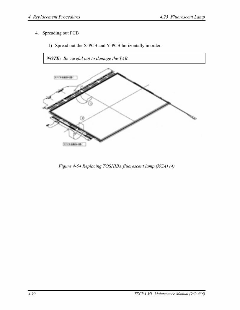
4 Replacement Procedures 4.25 Fluorescent Lamp
4. Spreading out PCB
1) Spread out the X-PCB and Y-PCB horizontally in order.
NOTE: Be careful not to damage the TAB.
Figure 4-54 Replacing TOSHIBA fluorescent lamp (XGA) (4)
4-90 TECRA M1 Maintenance Manual (960-436)
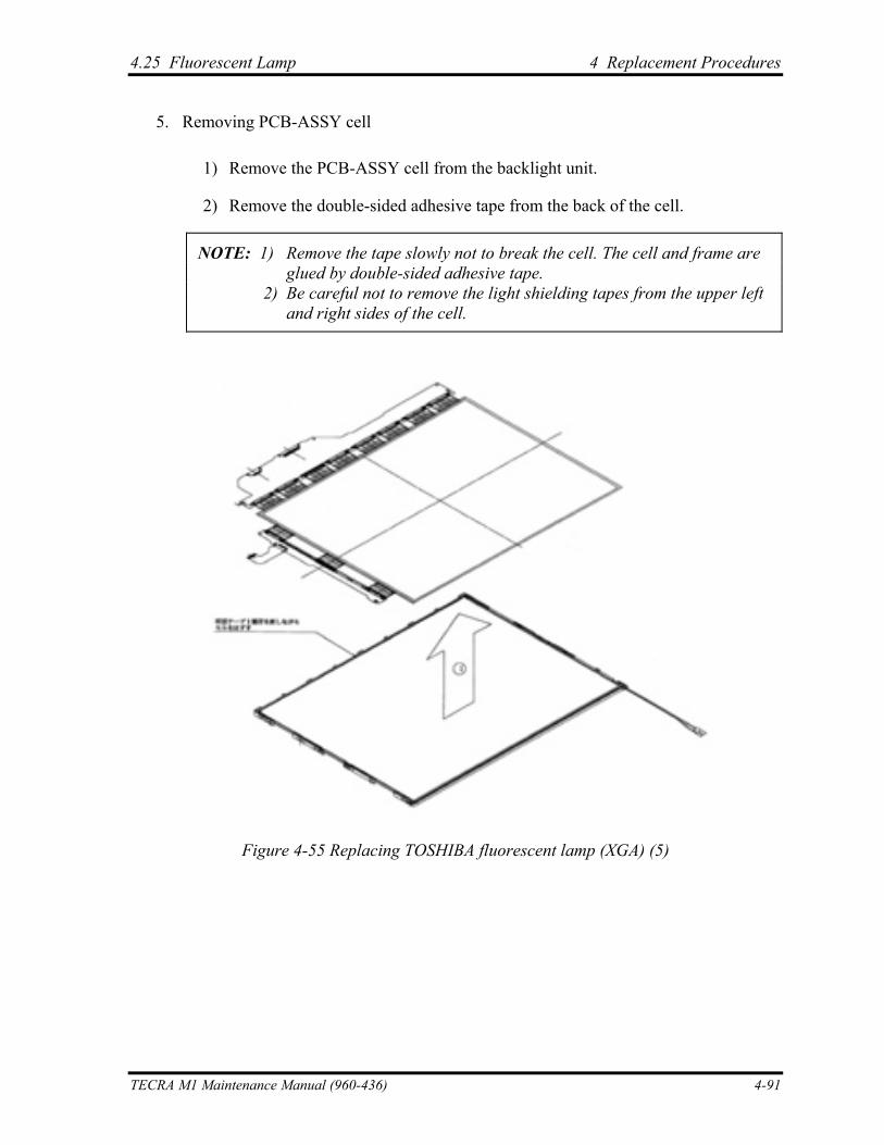
4.25 Fluorescent Lamp 4 Replacement Procedures
5. Removing PCB-ASSY cell
1) Remove the PCB-ASSY cell from the backlight unit.
2) Remove the double-sided adhesive tape from the back of the cell.
NOTE: 1) Remove the tape slowly not to break the cell. The cell and frame are glued by double-sided adhesive tape. 2) Be careful not to remove the light shielding tapes from the upper left and right sides of the cell.
Figure 4-55 Replacing TOSHIBA fluorescent lamp (XGA) (5)
TECRA M1 Maintenance Manual (960-436) 4-91
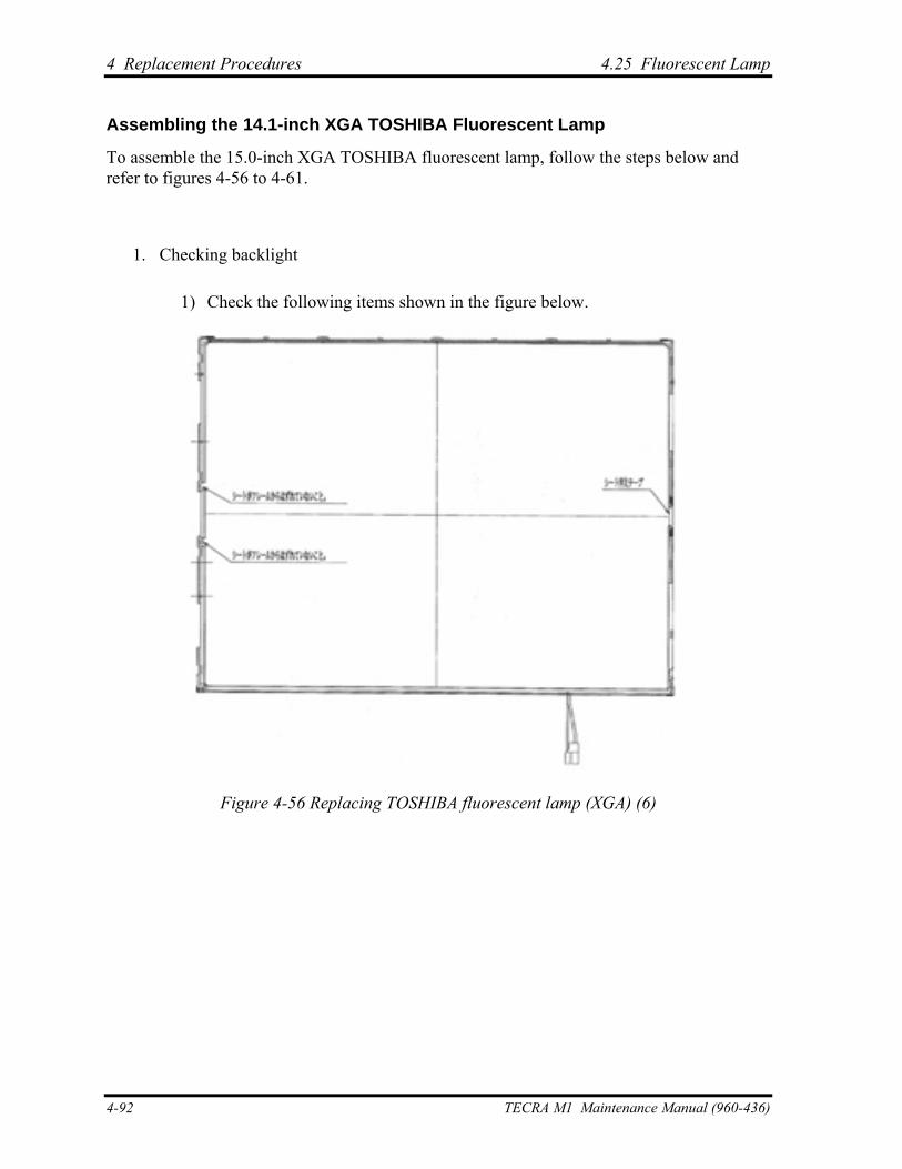
4 Replacement Procedures 4.25 Fluorescent Lamp
Assembling the 14.1-inch XGA TOSHIBA Fluorescent Lamp
To assemble the 15.0-inch XGA TOSHIBA fluorescent lamp, follow the steps below and refer to figures 4-56 to 4-61.
1. Checking backlight
1) Check the following items shown in the figure below.
Figure 4-56 Replacing TOSHIBA fluorescent lamp (XGA) (6)
4-92 TECRA M1 Maintenance Manual (960-436)
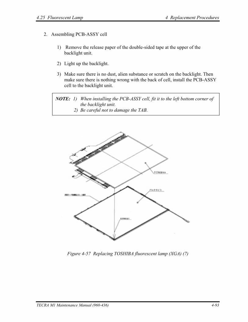
4.25 Fluorescent Lamp 4 Replacement Procedures
2. Assembling PCB-ASSY cell
1) Remove the release paper of the double-sided tape at the upper of the backlight unit.
2) Light up the backlight.
3) Make sure there is no dust, alien substance or scratch on the backlight. Then make sure there is nothing wrong with the back of cell, install the PCB-ASSY cell to the backlight unit.
NOTE: 1) When installing the PCB-ASSY cell, fit it to the left bottom corner of the backlight unit. 2) Be careful not to damage the TAB.
Figure 4-57 Replacing TOSHIBA fluorescent lamp (XGA) (7)
TECRA M1 Maintenance Manual (960-436) 4-93
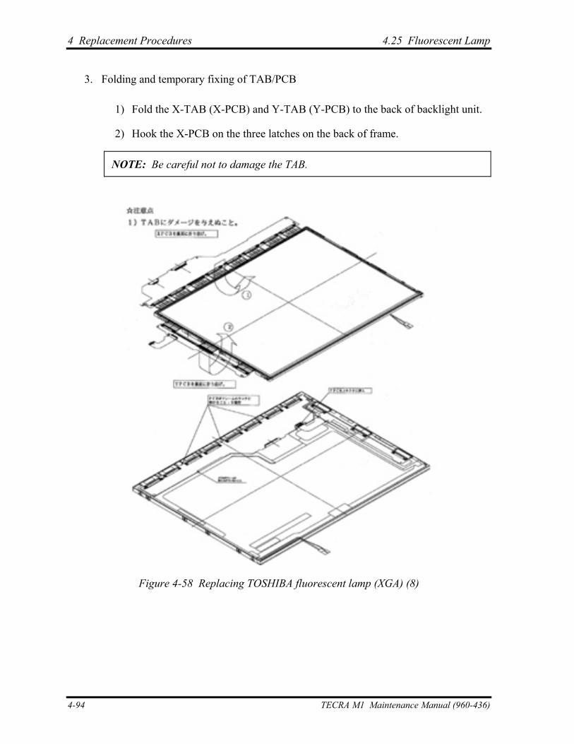
4 Replacement Procedures 4.25 Fluorescent Lamp
3. Folding and temporary fixing of TAB/PCB
1) Fold the X-TAB (X-PCB) and Y-TAB (Y-PCB) to the back of backlight unit.
2) Hook the X-PCB on the three latches on the back of frame.
NOTE: Be careful not to damage the TAB.
Figure 4-58 Replacing TOSHIBA fluorescent lamp (XGA) (8)
4-94 TECRA M1 Maintenance Manual (960-436)
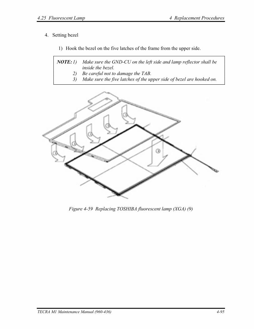
4.25 Fluorescent Lamp 4 Replacement Procedures
4. Setting bezel
1) Hook the bezel on the five latches of the frame from the upper side.
NOTE: 1) Make sure the GND-CU on the left side and lamp reflector shall be inside the bezel. 2) Be careful not to damage the TAB. 3) Make sure the five latches of the upper side of bezel are hooked on.
Figure 4-59 Replacing TOSHIBA fluorescent lamp (XGA) (9)
TECRA M1 Maintenance Manual (960-436) 4-95
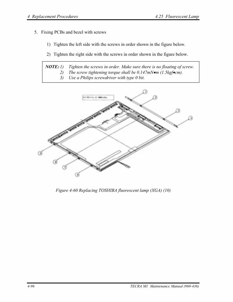
4 Replacement Procedures 4.25 Fluorescent Lamp
5. Fixing PCBs and bezel with screws
1) Tighten the left side with the screws in order shown in the figure below.
2) Tighten the right side with the screws in order shown in the figure below.
NOTE: 1) Tighten the screws in order. Make sure there is no floating of screw. 2) The screw tightening torque shall be 0.147mN•m (1.5kgf•cm). 3) Use a Philips screwdriver with type 0 bit.
Figure 4-60 Replacing TOSHIBA fluorescent lamp (XGA) (10)
4-96 TECRA M1 Maintenance Manual (960-436)
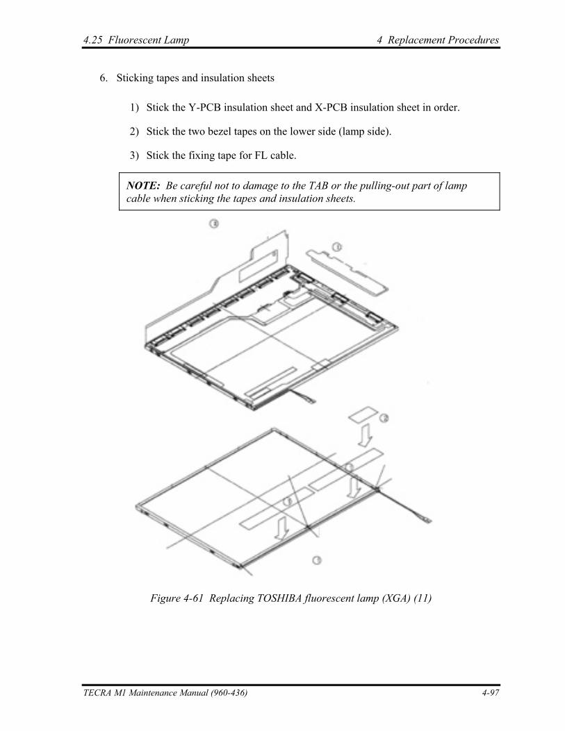
4.25 Fluorescent Lamp 4 Replacement Procedures
6. Sticking tapes and insulation sheets
1) Stick the Y-PCB insulation sheet and X-PCB insulation sheet in order.
2) Stick the two bezel tapes on the lower side (lamp side).
3) Stick the fixing tape for FL cable.
NOTE: Be careful not to damage to the TAB or the pulling-out part of lamp cable when sticking the tapes and insulation sheets.
Figure 4-61 Replacing TOSHIBA fluorescent lamp (XGA) (11)
TECRA M1 Maintenance Manual (960-436) 4-97
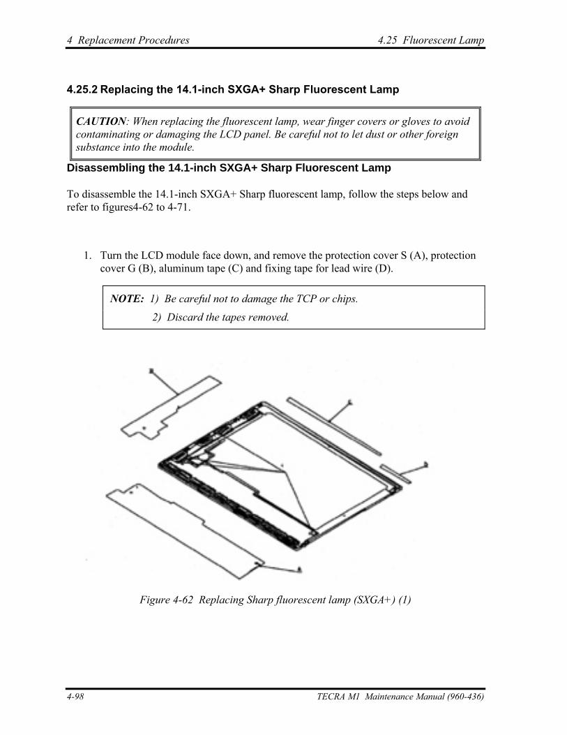
4 Replacement Procedures 4.25 Fluorescent Lamp
4.25.2 Replacing the 14.1-inch SXGA+ Sharp Fluorescent Lamp
CAUTION: When replacing the fluorescent lamp, wear finger covers or gloves to avoid contaminating or damaging the LCD panel. Be careful not to let dust or other foreign substance into the module.
Disassembling the 14.1-inch SXGA+ Sharp Fluorescent Lamp
To disassemble the 14.1-inch SXGA+ Sharp fluorescent lamp, follow the steps below and refer to figures4-62 to 4-71.
1. Turn the LCD module face down, and remove the protection cover S (A), protection cover G (B), aluminum tape (C) and fixing tape for lead wire (D).
NOTE: 1) Be careful not to damage the TCP or chips.
2) Discard the tapes removed.
Figure 4-62 Replacing Sharp fluorescent lamp (SXGA+) (1)
4-98 TECRA M1 Maintenance Manual (960-436)
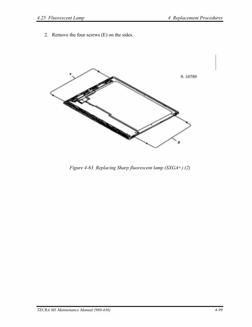
4.25 Fluorescent Lamp 4 Replacement Procedures
2. Remove the four screws (E) on the sides.
Figure 4-63 Replacing Sharp fluorescent lamp (SXGA+) (2)
TECRA M1 Maintenance Manual (960-436) 4-99
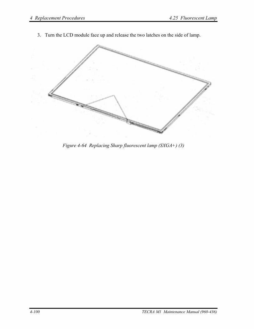
4 Replacement Procedures 4.25 Fluorescent Lamp
3. Turn the LCD module face up and release the two latches on the side of lamp.
Figure 4-64 Replacing Sharp fluorescent lamp (SXGA+) (3)
4-100 TECRA M1 Maintenance Manual (960-436)
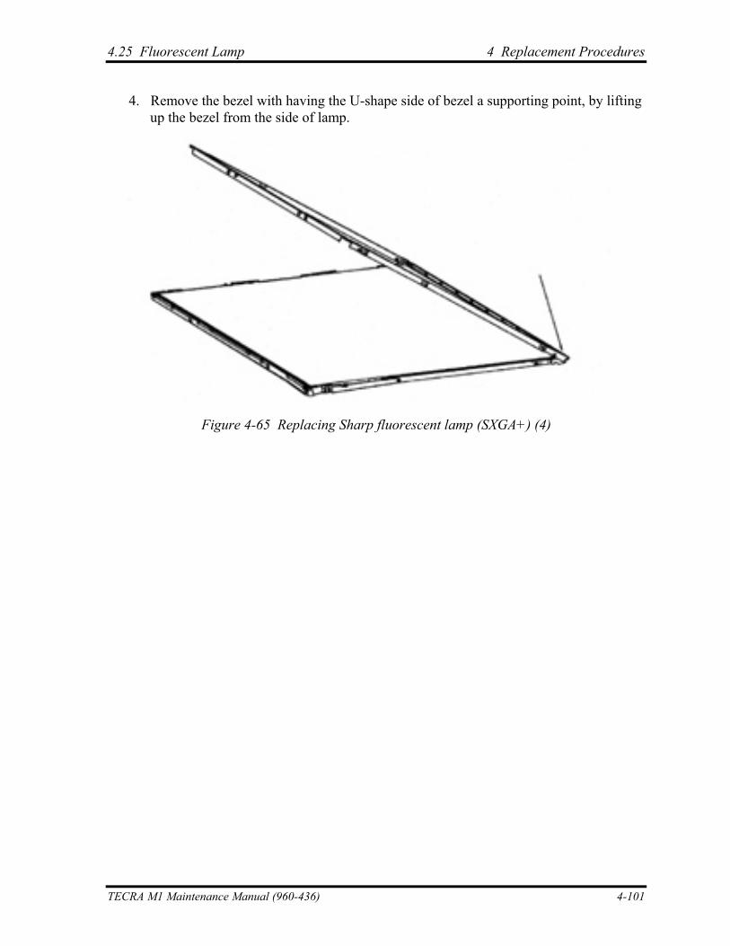
4.25 Fluorescent Lamp 4 Replacement Procedures
4. Remove the bezel with having the U-shape side of bezel a supporting point, by lifting up the bezel from the side of lamp.
Figure 4-65 Replacing Sharp fluorescent lamp (SXGA+) (4)
TECRA M1 Maintenance Manual (960-436) 4-101
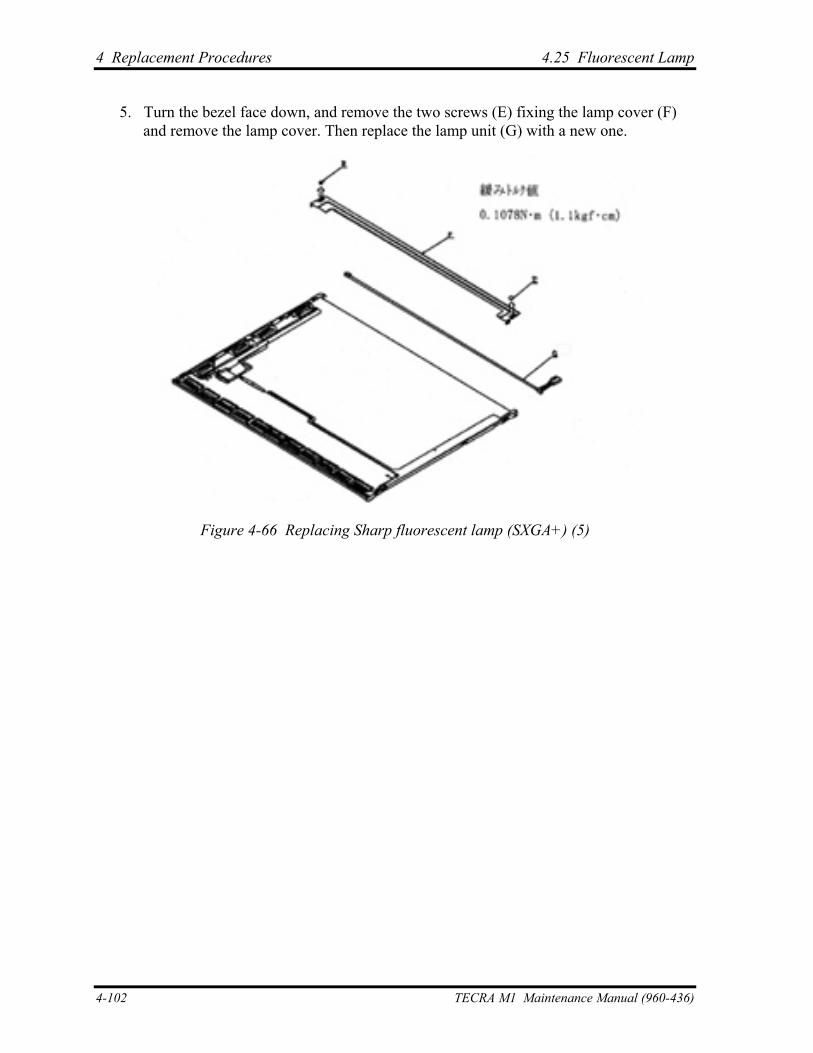
4 Replacement Procedures 4.25 Fluorescent Lamp
5. Turn the bezel face down, and remove the two screws (E) fixing the lamp cover (F) and remove the lamp cover. Then replace the lamp unit (G) with a new one.
Figure 4-66 Replacing Sharp fluorescent lamp (SXGA+) (5)
4-102 TECRA M1 Maintenance Manual (960-436)
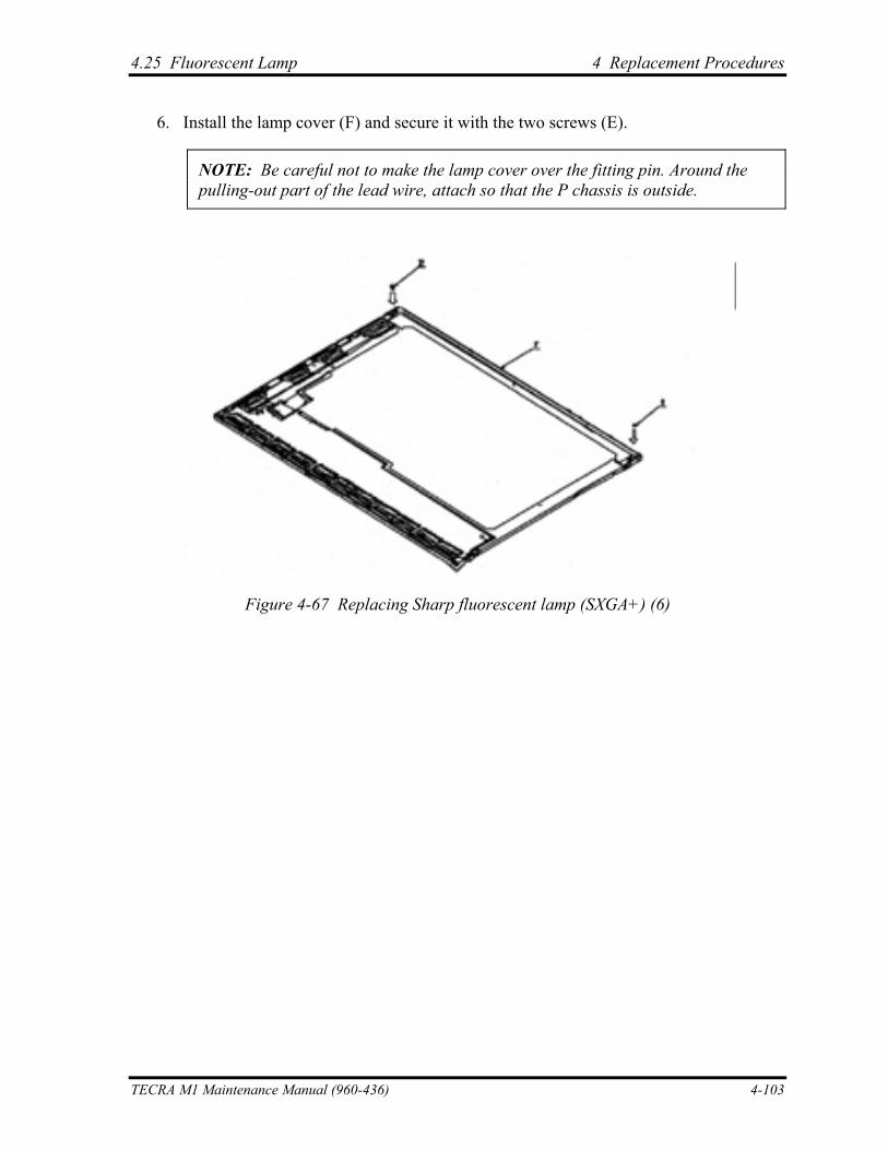
4.25 Fluorescent Lamp 4 Replacement Procedures
6. Install the lamp cover (F) and secure it with the two screws (E).
NOTE: Be careful not to make the lamp cover over the fitting pin. Around the pulling-out part of the lead wire, attach so that the P chassis is outside.
Figure 4-67 Replacing Sharp fluorescent lamp (SXGA+) (6)
TECRA M1 Maintenance Manual (960-436) 4-103
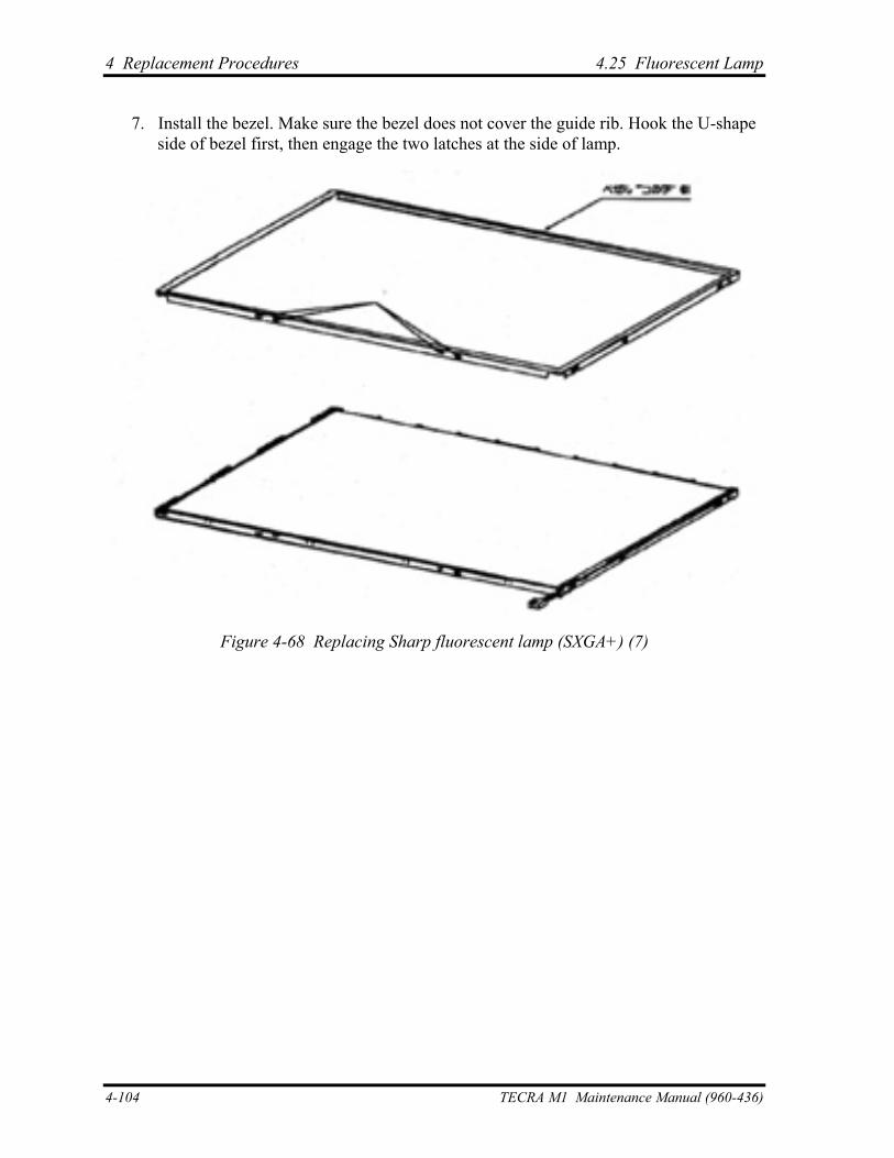
4 Replacement Procedures 4.25 Fluorescent Lamp
7. Install the bezel. Make sure the bezel does not cover the guide rib. Hook the U-shape side of bezel first, then engage the two latches at the side of lamp.
Figure 4-68 Replacing Sharp fluorescent lamp (SXGA+) (7)
4-104 TECRA M1 Maintenance Manual (960-436)
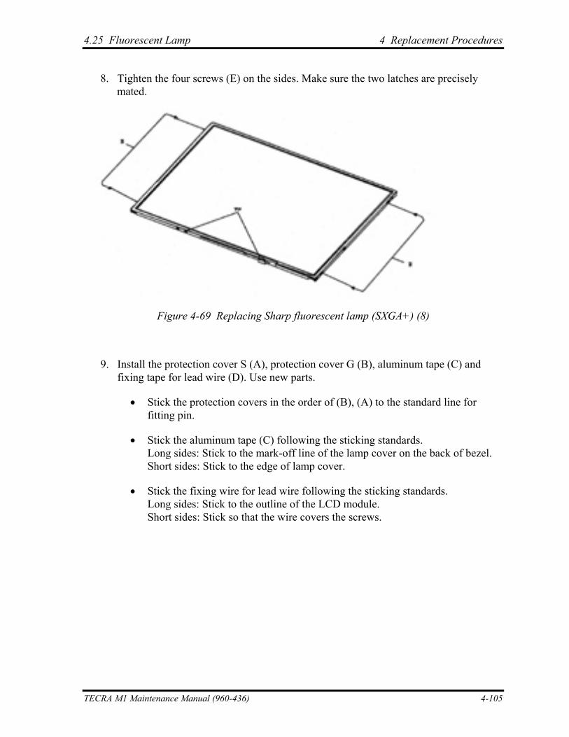
4.25 Fluorescent Lamp 4 Replacement Procedures
8. Tighten the four screws (E) on the sides. Make sure the two latches are precisely mated.
Figure 4-69 Replacing Sharp fluorescent lamp (SXGA+) (8)
9. Install the protection cover S (A), protection cover G (B), aluminum tape (C) and fixing tape for lead wire (D). Use new parts.
• Stick the protection covers in the order of (B), (A) to the standard line for fitting pin.
• Stick the aluminum tape (C) following the sticking standards. Long sides: Stick to the mark-off line of the lamp cover on the back of bezel. Short sides: Stick to the edge of lamp cover.
• Stick the fixing wire for lead wire following the sticking standards. Long sides: Stick to the outline of the LCD module. Short sides: Stick so that the wire covers the screws.
TECRA M1 Maintenance Manual (960-436) 4-105
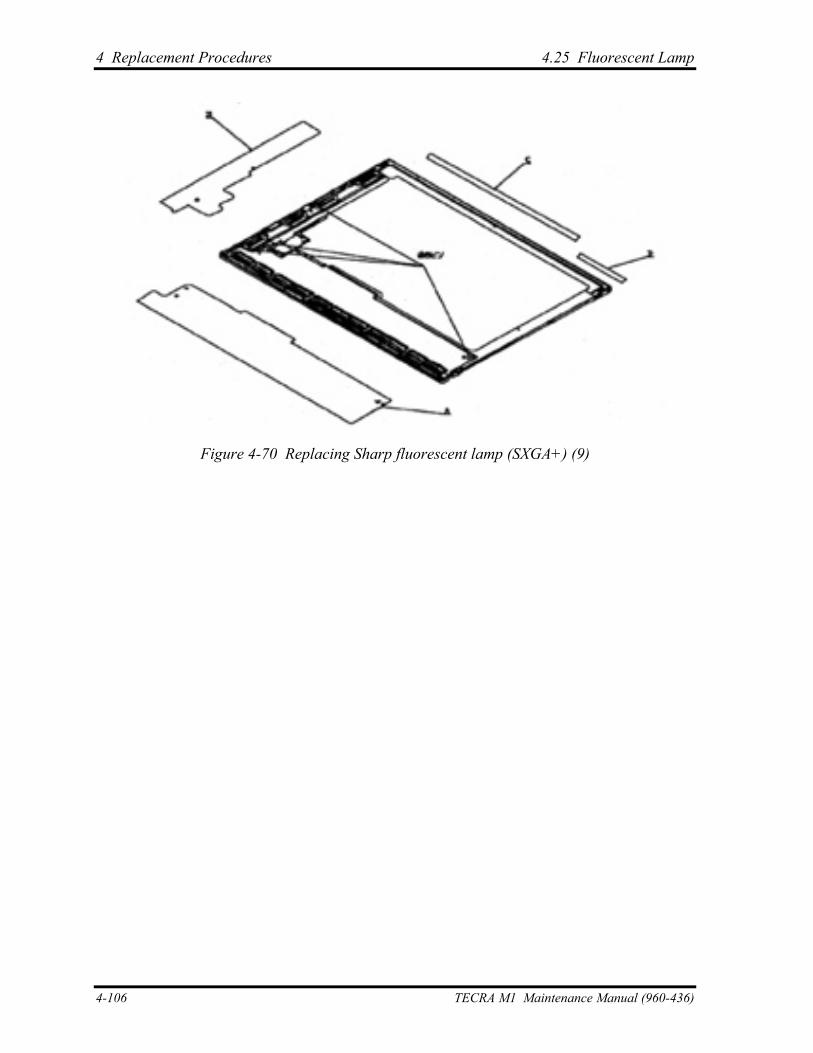
4 Replacement Procedures 4.25 Fluorescent Lamp
Figure 4-70 Replacing Sharp fluorescent lamp (SXGA+) (9)
4-106 TECRA M1 Maintenance Manual (960-436)
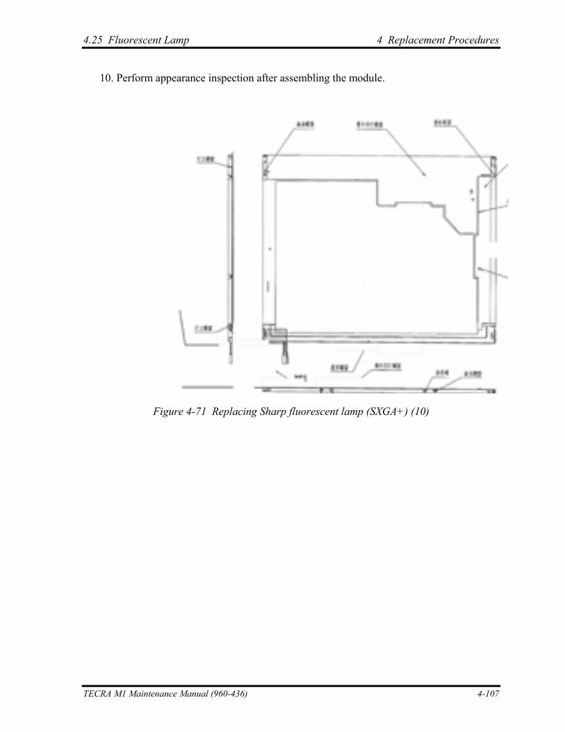
4.25 Fluorescent Lamp 4 Replacement Procedures
10. Perform appearance inspection after assembling the module.
Figure 4-71 Replacing Sharp fluorescent lamp (SXGA+) (10)
TECRA M1 Maintenance Manual (960-436) 4-107
4 Replacement Procedures 4.25 Fluorescent Lamp
4-108 TECRA M1 Maintenance Manual (960-436)
Assembling the 14.1-inch SXGA+ Sharp Fluorescent Lamp
To assemble the 14.1-inch Sharp SXGA+ fluorescent lamp, follow the steps below and refer to figures 4-62 to 4-71.
Appendices

Appendices
App-ii
Appendices
Appendix Contents
Appendix A Handling the LCD Module .......................................................................... A-1
Appendix B Board Layout .................................................................................................B-1 B.1 System Board (FGFSY*) Front View........................................................................1
B.2 System Board (FGFSY*) Back View ........................................................................3
B.3 Sound Board (FGFSD*) Front and Back View .........................................................5
B.4 LED Board (FGFLE*) Front and Back View ............................................................6
B.5 Sensor/Switch Board (FGFLS*) Front and Back View.............................................7
B.6 USB Board (FGFUS*) Front and Back View............................................................8
Appendix C Pin Assignments............................................................................................ C-1 C.1 PJ1001 Memory 1 connector (200-pin) ...............................................................C-1
C.2 PJ1002 Memory 2 connector (200-pin) ...............................................................C-4
C.3 PJ1509 HDD interface connector (44-pin)...........................................................C-7
C.4 PJ1511 Select Bay interface connector (72-pin) ..................................................C-8
C.5 PJ1512 PC-Card interface connector (150-pin) ...................................................C-9
C.6 PJ1514 SD Card interface connector (12-pin) ...................................................C-11
C.7 PJ123 Keyboard interface connector (34-pin) ...................................................C-11
C.8 PJ2003 PAD interface connector (8-pin) ...........................................................C-12
C.9 PJ1101 LED board interface connector (14-pin) ...............................................C-12
C.10 PJ1000 Sensor/Switch board interface connector (10-pin) ................................C-12
C.11 PJ2026 Speaker (Right) connector (3-pin).........................................................C-12
C.12 PJ2027 Speaker (Left) connector (2-pin) ...........................................................C-13
C.13 PJ2007 Docking connector (240-pin) ................................................................C-14
C.14 PJ2015 Mini PCI interface connector (124-pin) ................................................C-17
C.15 PJ2017 MDC 1 interface connector (30-pin) .....................................................C-19
C.16 PJ1003 MDC 2 interface connector (2-pin) .......................................................C-19
C.17 PJ2019 Serial interface connector (9-pin)..........................................................C-19
C.18 PJ2020 Parallel interface connector (25-pin) .....................................................C-20
C.19 PJ2033 USB 0 interface connector (4-pin) ........................................................C-20
C.20 PJ2034 USB 1 interface connector (4-pin) ........................................................C-20
App-iii
Appendices
C.21 PJ1004 USB baord interface connector (6-pin) .................................................C-20
C.22 PJ4900 Bluetooth interface connector (20-pin) .................................................C-21
C.23 PJ1100 Sound board interface connector (30-pin).............................................C-21
C.24 PJ651 IEEE1394 interface connector (4-pin).....................................................C-22
C.25 PJ4500 LAN interface connector (14-pin) .........................................................C-22
C.26 PJ8800 DC-IN connector (4-pin) .......................................................................C-22
C.27 PJ8810 1st Battery connector (10-pin)...............................................................C-22
C.28 PJ1005 RTC Battery connector (2-pin)..............................................................C-23
C.29 PJ8770 FAN interface connector (3-pin) ...........................................................C-23
C.30 PJ5500 LCD interface connector (41-pin) .........................................................C-23
C.31 PJ5523 CRT interface connector (15-pin) .........................................................C-24
C.32 PJ5501 TV connector (4-pin).............................................................................C-24
C.33 PJ3000 System board interface connector (30-pin) ...........................................C-25
C.34 PJ3001 Internal Microphone connector (2-pin) .................................................C-25
C.35 PJ3002 External Microphone connector (6-pin) ................................................C-25
C.36 PJ3003 Headphone connector (6-pin) ................................................................C-26
C.37 PJ3100 System board interface connector (14-pin) ...........................................C-27
C.38 PJ3200 System board interface connector (10-pin) ...........................................C-28
C.39 PJ3300 System board interface connector (6-pin) .............................................C-29
C.40 PJ3301 USB port 2 interface connector (4-pin) .................................................C-29
Appendix D Keyboard Scan/Character Codes................................................................ D-1
Appendix E Key Layout .....................................................................................................E-1
E.1 United Kingdom (UK) Keyboard...........................................................................E-1
E.2 United States (US) Keyboard.................................................................................E-1
Appendix F Wiring Diagrams ...........................................................................................F-1
F.1 Parallel Port Wraparound Connector .....................................................................F-1
F.2 Serial Port Wraparound Connector ........................................................................F-1
F.3 LAN Loopback Connector .....................................................................................F-2
Appendix G BIOS Rewrite Procedures ........................................................................... G-1
App-iv
Appendices
Appendix H EC/KBC Rewrite Procedures...................................................................... H-1
Appendix I Reliability .........................................................................................................I-1
App-v
Appendices
Figures
Figure B-1 System board (FGFSY*) layout (front).................................................................1
Figure B-2 System board (FGFSY*) layout (back).................................................................3
Figure B-3 Sound board (FGFSD*) layout (front/back) .........................................................5
Figure B-4 LED board (FGFLE*) layout (front/back) ............................................................6
Figure B-5 Sensor/Switch board (FGFLS*) layout (front/back) .............................................7
Figure B-6 USB board (FGFUS*) layout (front/back) ............................................................8
Figure E-1 UK keyboard......................................................................................................E-1
Figure E-2 US keyboard ......................................................................................................E-1
Figure F-1 Parallel port wraparound connector..................................................................F-1
Figure F-2 Serial port wraparound connector.....................................................................F-1
Figure F-3 LAN loopback connector..................................................................................F-2
App-vi
Appendices
Tables
Table B-1 System board (FGFSY*) ICs and connectors (front) .............................................2
Table B-2 System board (FGFSY*) ICs and connectors (back) .............................................4
Table B-3 Sound board (FGFSD*) ICs and connectors (front/back) ......................................5
Table B-4 LED board (FGFLE*) connectors (front)...............................................................6
Table B-5 Sensor/Switch board (FGFLS*) ICs and connectors (front/back)..........................7
Table B-6 USB board (FGFUS*) connectors (back)...............................................................8
TableC-1 Memory 1 connector (200-pin)............................................................................C-1
TableC-2 Memory 2 connector (200-pin)............................................................................C-4
TableC-3 HDD interface connector (44-pin).......................................................................C-7
TableC-4 Select Bay interface connector (72-pin) ..............................................................C-8
TableC-5 PC-Card interface connector (150-pin) ...............................................................C-9
TableC-6 SD Card interface connector (12-pin)................................................................C-11
TableC-7 Keyboard interface connector (34-pin).............................................................C-11
TableC-8 PAD interface connector (8-pin) .......................................................................C-12
TableC-9 LED board interface connector (14-pin)............................................................C-12
TableC-10 Sensor/Switch board interface connector (10-pin) ..........................................C-12
TableC-11 Speaker (Right) connector (3-pin) ...................................................................C-12
TableC-12 Speaker (Left) connector (2-pin) .....................................................................C-13
TableC-13 Docking interface connector (240-pin)............................................................C-14
TableC-14 Mini PCI interface connector (124-pin) ..........................................................C-17
TableC-15 MDC 1 interface connector (30-pin) ...............................................................C-19
TableC-16 MDC 2 interface connector (2-pin) .................................................................C-19
TableC-17 Serial interface connector (9-pin) ....................................................................C-19
TableC-18 Parallel interface connector (25-pin) ...............................................................C-20
TableC-19 USB 0 interface connector (4-pin)...................................................................C-20
TableC-20 USB 1 interface connector (4-pin)...................................................................C-20
TableC-21 USB board interface connector (6-pin)............................................................C-20
TableC-22 Bluetooth interface connector (20-pin)............................................................C-21
App-vii
Appendices
App-viii
TableC-23 Sound board interface connector (30-pin) .......................................................C-21
TableC-24 IEEE1394 interface connector (4-pin).............................................................C-22
TableC-25 LAN interface connector (14-pin) ...................................................................C-22
TableC-26 DC-IN interface connector (4-pin) ..................................................................C-22
TableC-27 1st Battery connector (10-pin) .........................................................................C-22
TableC-28 RTC Battery connector (2-pin) ........................................................................C-23
TableC-29 FAN interface connector (3in).........................................................................C-23
TableC-30 LCD interface connector (41-pin) ...................................................................C-23
TableC-31 CRT interface connector (15-pin)....................................................................C-24
TableC-32 TV interface connector (4-pin) ........................................................................C-24
TableC-33 System board interface connector (30-pin)......................................................C-25
TableC-34 Internal Microphone connector (2-pin) ...........................................................C-25
TableC-35 External Microphone connector (6-pin) ..........................................................C-25
TableC-36 Headphone connector (6-pin) ..........................................................................C-26
TableC-37 System board interface connector (14-pin)......................................................C-27
TableC-38 System board interface connector (10-pin)......................................................C-28
TableC-39 System board interface connector (6-pin)........................................................C-29
TableC-40 USB port 2 interface connector (4-pin) ...........................................................C-29
Table D-1 Scan codes (set 1 and set 2) ............................................................................... D-1
Table D-2 Scan codes with left Shift key ............................................................................ D-5
Table D-3 Scan codes in Numlock mode ............................................................................ D-6
Table D-4 Scan codes with Fn key ...................................................................................... D-6
Table D-5 Scan codes in overlay mode ............................................................................... D-7
Table D-6 No.124 key scan code......................................................................................... D-7
Table D-7 No.126 key scan code......................................................................................... D-8
Table I-1 MTBF..............................................................................................................I-1
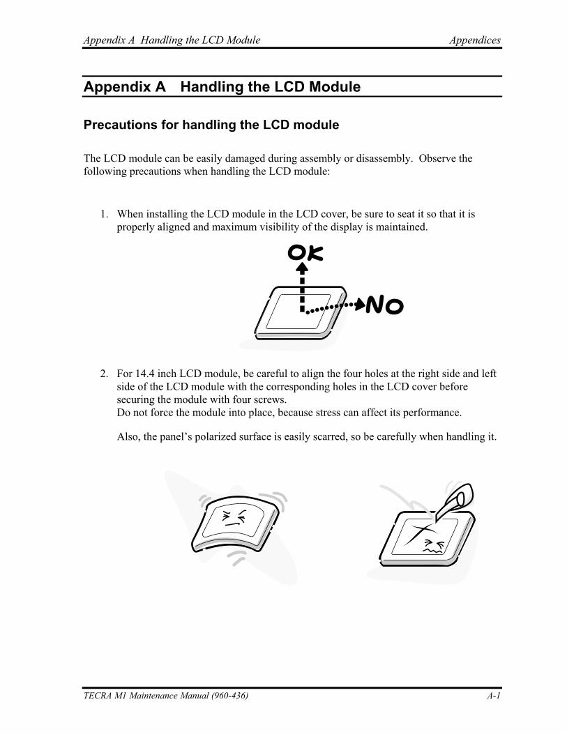
Appendix A Handling the LCD Module Appendices
Appendix A P
Appendix A Handling the LCD Module
Precautions for handling the LCD module
The LCD module can be easily damaged during assembly or disassembly. Observe the following precautions when handling the LCD module:
1. When installing the LCD module in the LCD cover, be sure to seat it so that it is properly aligned and maximum visibility of the display is maintained.
2. For 14.4 inch LCD module, be careful to align the four holes at the right side and left side of the LCD module with the corresponding holes in the LCD cover before securing the module with four screws. Do not force the module into place, because stress can affect its performance.
Also, the panel’s polarized surface is easily scarred, so be carefully when handling it.
TECRA M1 Maintenance Manual (960-436) A-1
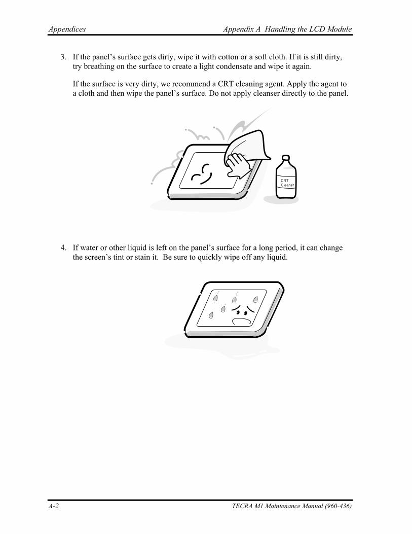
Appendices Appendix A Handling the LCD Module
3. If the panel’s surface gets dirty, wipe it with cotton or a soft cloth. If it is still dirty, try breathing on the surface to create a light condensate and wipe it again.
If the surface is very dirty, we recommend a CRT cleaning agent. Apply the agent to a cloth and then wipe the panel’s surface. Do not apply cleanser directly to the panel.
CRTCleaner
4. If water or other liquid is left on the panel’s surface for a long period, it can change the screen’s tint or stain it. Be sure to quickly wipe off any liquid.
A-2 TECRA M1 Maintenance Manual (960-436)
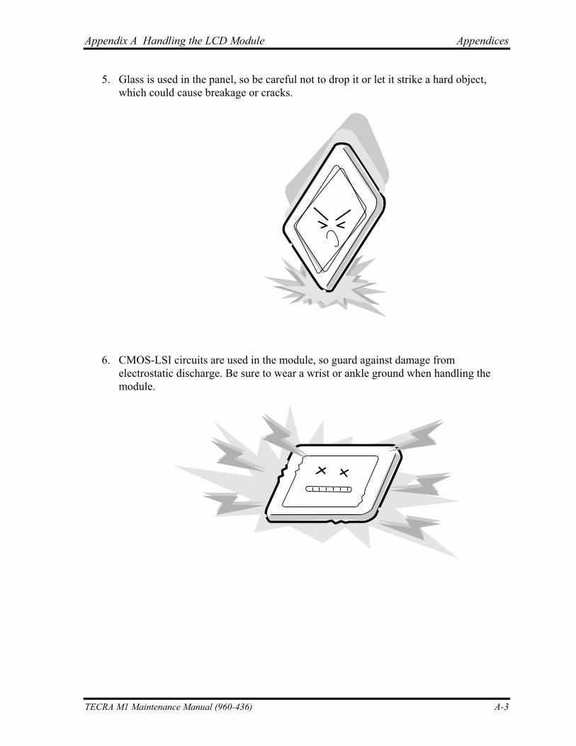
Appendix A Handling the LCD Module Appendices
5. Glass is used in the panel, so be careful not to drop it or let it strike a hard object, which could cause breakage or cracks.
6. CMOS-LSI circuits are used in the module, so guard against damage from electrostatic discharge. Be sure to wear a wrist or ankle ground when handling the module.
TECRA M1 Maintenance Manual (960-436) A-3
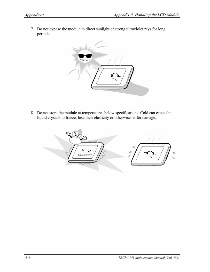
Appendices Appendix A Handling the LCD Module
7. Do not expose the module to direct sunlight or strong ultraviolet rays for long periods.
8. Do not store the module at temperatures below specifications. Cold can cause the liquid crystals to freeze, lose their elasticity or otherwise suffer damage.
A-4 TECRA M1 Maintenance Manual (960-436)
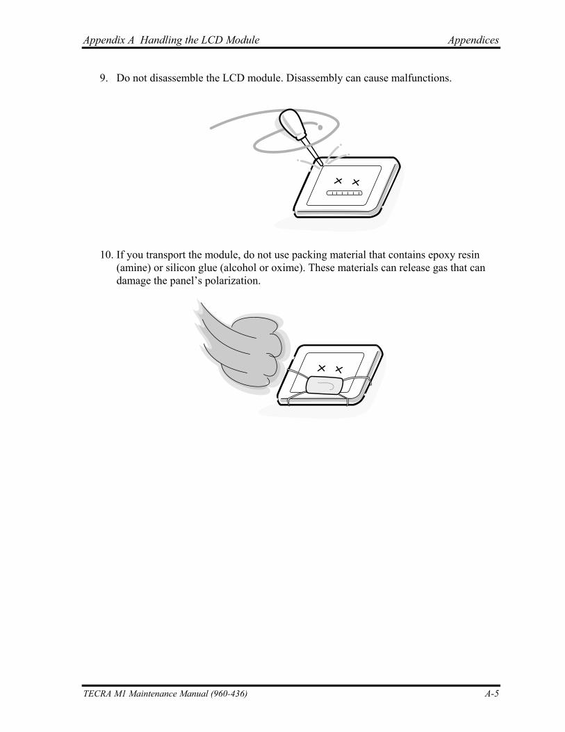
Appendix A Handling the LCD Module Appendices
9. Do not disassemble the LCD module. Disassembly can cause malfunctions.
10. If you transport the module, do not use packing material that contains epoxy resin (amine) or silicon glue (alcohol or oxime). These materials can release gas that can damage the panel’s polarization.
TECRA M1 Maintenance Manual (960-436) A-5
Appendices Appendix A Handling the LCD Module
A-6 TECRA M1 Maintenance Manual (960-436)
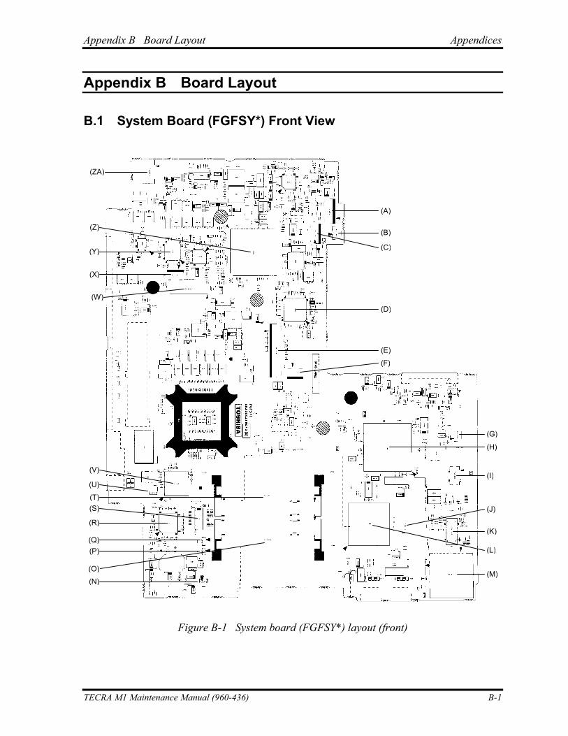
Appendix B Board Layout Appendices
Appendix B Board Layout
B.1 System Board (FGFSY*) Front View
(ZA)
(Z)
(Y)
(X)
(W)
(V)
(U)
(T)(S)
(R)
(Q)(P)
(O)(N)
(A)
(B)
(C)
(D)
(E)
(F)
(M)
(L)
(K)
(J)
(I)
(H)
(G)
Figure B-1 System board (FGFSY*) layout (front)
TECRA M1 Maintenance Manual (960-436) B-1
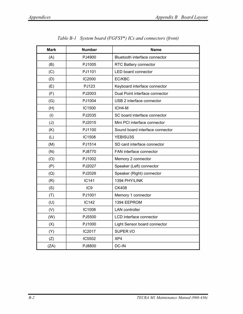
Appendices Appendix B Board Layout
Table B-1 System board (FGFSY*) ICs and connectors (front)
Mark Number Name
(A) PJ4900 Bluetooth interface connector
(B) PJ1005 RTC Battery connector
(C) PJ1101 LED board connector
(D) IC2000 EC/KBC
(E) PJ123 Keyboard interface connector
(F) PJ2003 Dual Point interface connector
(G) PJ1004 USB 2 interface connector
(H) IC1500 ICH4-M
(I) PJ2035 SC board interface connector
(J) PJ2015 Mini PCI interface connector
(K) PJ1100 Sound board interface connector
(L) IC1508 YEBISU3S
(M) PJ1514 SD card interface connector
(N) PJ8770 FAN interface connector
(O) PJ1002 Memory 2 connector
(P) PJ2027 Speaker (Left) connector
(Q) PJ2026 Speaker (Right) connector
(R) IC141 1394 PHY/LINK
(S) IC9 CK408
(T) PJ1001 Memory 1 connector
(U) IC142 1394 EEPROM
(V) IC1008 LAN controller
(W) PJ5500 LCD interface connector
(X) PJ1000 Light Sensor board connector
(Y) IC2017 SUPER I/O
(Z) IC5502 XP4
(ZA) PJ8800 DC-IN
B-2 TECRA M1 Maintenance Manual (960-436)
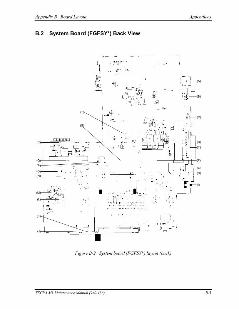
Appendix B Board Layout Appendices
B.2 System Board (FGFSY*) Back View
(T)
(S)
(R)
(Q)
(P)
(O)(N)
(M)
(L)
(J)
(K)
(A)
(B)
(C)
(D)
(E)
(F)
(G)(H)
(I)
Figure B-2 System board (FGFSY*) layout (back)
TECRA M1 Maintenance Manual (960-436) B-3
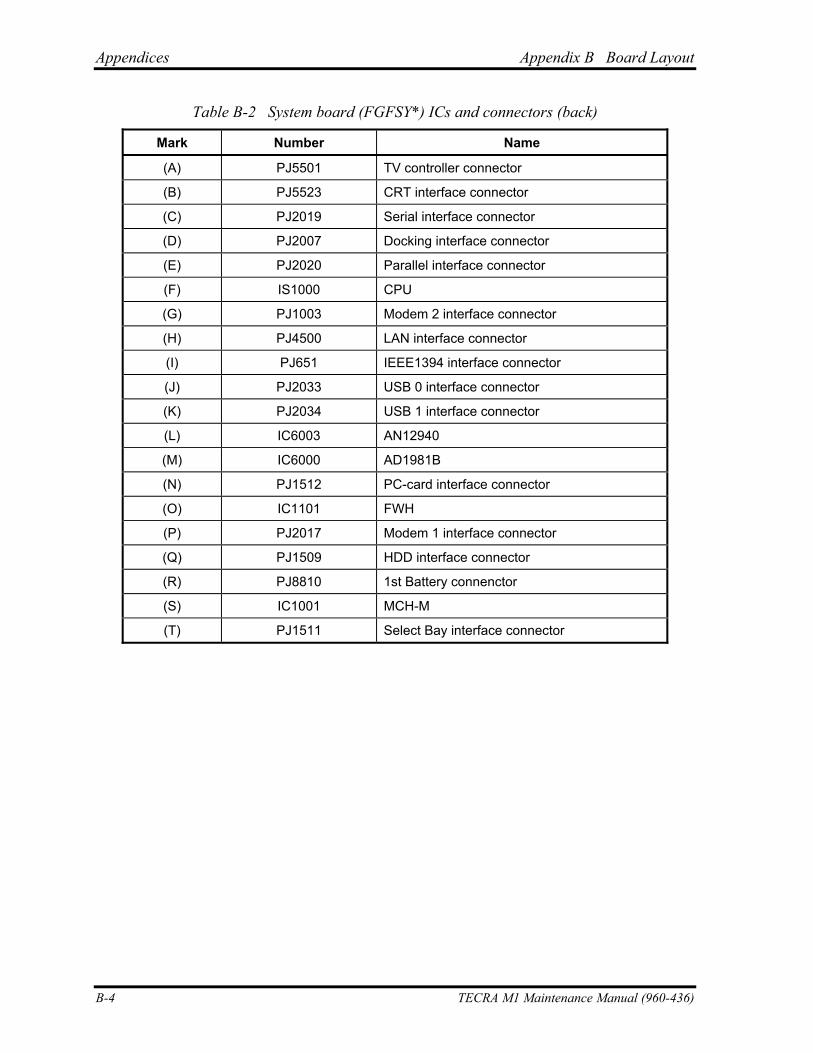
Appendices Appendix B Board Layout
Table B-2 System board (FGFSY*) ICs and connectors (back)
Mark Number Name
(A) PJ5501 TV controller connector
(B) PJ5523 CRT interface connector
(C) PJ2019 Serial interface connector
(D) PJ2007 Docking interface connector
(E) PJ2020 Parallel interface connector
(F) IS1000 CPU
(G) PJ1003 Modem 2 interface connector
(H) PJ4500 LAN interface connector
(I) PJ651 IEEE1394 interface connector
(J) PJ2033 USB 0 interface connector
(K) PJ2034 USB 1 interface connector
(L) IC6003 AN12940
(M) IC6000 AD1981B
(N) PJ1512 PC-card interface connector
(O) IC1101 FWH
(P) PJ2017 Modem 1 interface connector
(Q) PJ1509 HDD interface connector
(R) PJ8810 1st Battery connenctor
(S) IC1001 MCH-M
(T) PJ1511 Select Bay interface connector
B-4 TECRA M1 Maintenance Manual (960-436)
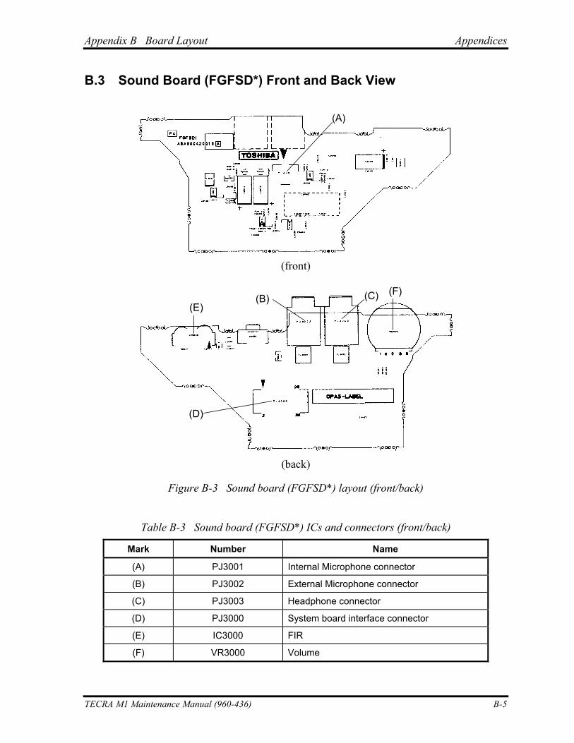
Appendix B Board Layout Appendices
B.3 Sound Board (FGFSD*) Front and Back View
(A)
(front)
(E)(B) (C) (F)
(D)
(back)
Figure B-3 Sound board (FGFSD*) layout (front/back)
Table B-3 Sound board (FGFSD*) ICs and connectors (front/back)
Mark Number Name
(A) PJ3001 Internal Microphone connector
(B) PJ3002 External Microphone connector
(C) PJ3003 Headphone connector
(D) PJ3000 System board interface connector
(E) IC3000 FIR
(F) VR3000 Volume
TECRA M1 Maintenance Manual (960-436) B-5
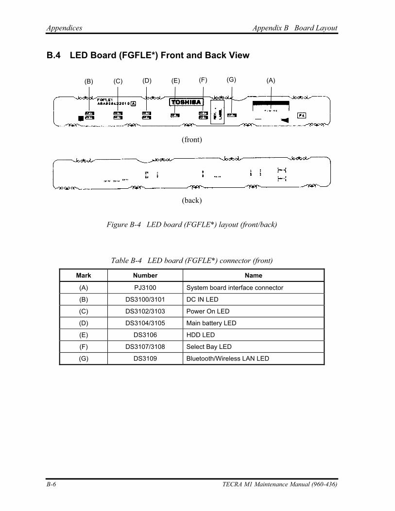
Appendices Appendix B Board Layout
B.4 LED Board (FGFLE*) Front and Back View
(B) (C) (D) (E) (F) (G) (A)
(front)
(back)
Figure B-4 LED board (FGFLE*) layout (front/back)
Table B-4 LED board (FGFLE*) connector (front)
Mark Number Name
(A) PJ3100 System board interface connector
(B) DS3100/3101 DC IN LED
(C) DS3102/3103 Power On LED
(D) DS3104/3105 Main battery LED
(E) DS3106 HDD LED
(F) DS3107/3108 Select Bay LED
(G) DS3109 Bluetooth/Wireless LAN LED
B-6 TECRA M1 Maintenance Manual (960-436)
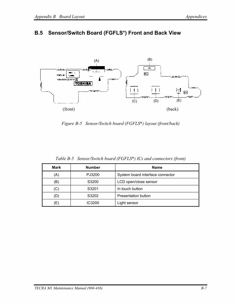
Appendix B Board Layout Appendices
B.5 Sensor/Switch Board (FGFLS*) Front and Back View
(A)
(C) (D) (E)
(B)
(front) (back)
Figure B-5 Sensor/Switch board (FGFLS*) layout (front/back)
Table B-5 Sensor/Switch board (FGFLS*) ICs and connectors (front)
Mark Number Name
(A) PJ3200 System board interface connector
(B) S3200 LCD open/close sensor
(C) S3201 In touch button
(D) S3202 Presentation button
(E) IC3200 Light sensor
TECRA M1 Maintenance Manual (960-436) B-7
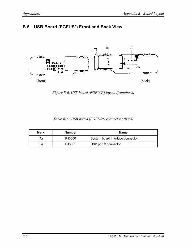
Appendices Appendix B Board Layout
B-8 TECRA M1 Maintenance Manual (960-436)
B.6 USB Board (FGFUS*) Front and Back View
(A)(B)
(front) (back)
Figure B-6 USB board (FGFUS*) layout (front/back)
Table B-6 USB board (FGFUS*) connectors (back)
Mark Number Name
(A) PJ3300 System board interface connector
(B) PJ3301 USB port 3 connector
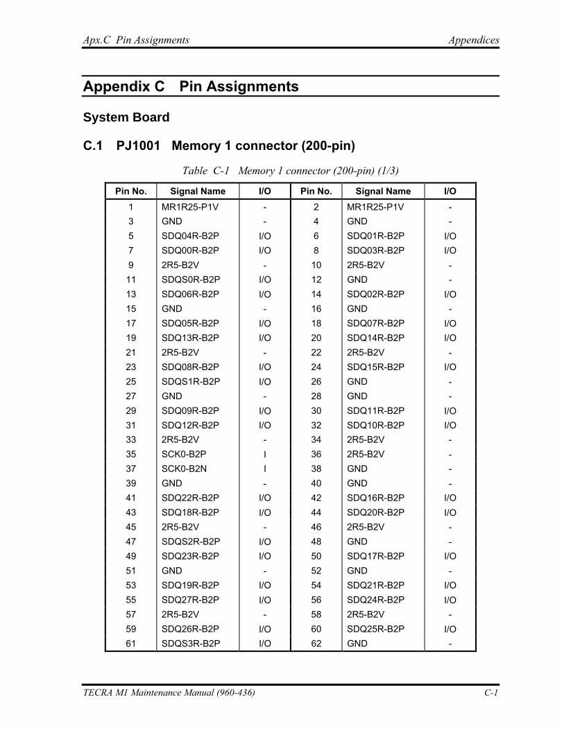
Apx.C Pin Assignments Appendices
Appendix C
Appendix C Pin Assignments
System Board
C.1 PJ1001 Memory 1 connector (200-pin)
Table C-1 Memory 1 connector (200-pin) (1/3)
Pin No. Signal Name I/O Pin No. Signal Name I/O 1 MR1R25-P1V - 2 MR1R25-P1V - 3 GND - 4 GND - 5 SDQ04R-B2P I/O 6 SDQ01R-B2P I/O 7 SDQ00R-B2P I/O 8 SDQ03R-B2P I/O 9 2R5-B2V - 10 2R5-B2V - 11 SDQS0R-B2P I/O 12 GND - 13 SDQ06R-B2P I/O 14 SDQ02R-B2P I/O 15 GND - 16 GND - 17 SDQ05R-B2P I/O 18 SDQ07R-B2P I/O 19 SDQ13R-B2P I/O 20 SDQ14R-B2P I/O 21 2R5-B2V - 22 2R5-B2V - 23 SDQ08R-B2P I/O 24 SDQ15R-B2P I/O 25 SDQS1R-B2P I/O 26 GND - 27 GND - 28 GND - 29 SDQ09R-B2P I/O 30 SDQ11R-B2P I/O 31 SDQ12R-B2P I/O 32 SDQ10R-B2P I/O 33 2R5-B2V - 34 2R5-B2V - 35 SCK0-B2P I 36 2R5-B2V - 37 SCK0-B2N I 38 GND - 39 GND - 40 GND - 41 SDQ22R-B2P I/O 42 SDQ16R-B2P I/O 43 SDQ18R-B2P I/O 44 SDQ20R-B2P I/O 45 2R5-B2V - 46 2R5-B2V - 47 SDQS2R-B2P I/O 48 GND - 49 SDQ23R-B2P I/O 50 SDQ17R-B2P I/O 51 GND - 52 GND - 53 SDQ19R-B2P I/O 54 SDQ21R-B2P I/O 55 SDQ27R-B2P I/O 56 SDQ24R-B2P I/O 57 2R5-B2V - 58 2R5-B2V - 59 SDQ26R-B2P I/O 60 SDQ25R-B2P I/O 61 SDQS3R-B2P I/O 62 GND -
TECRA M1 Maintenance Manual (960-436) C-1
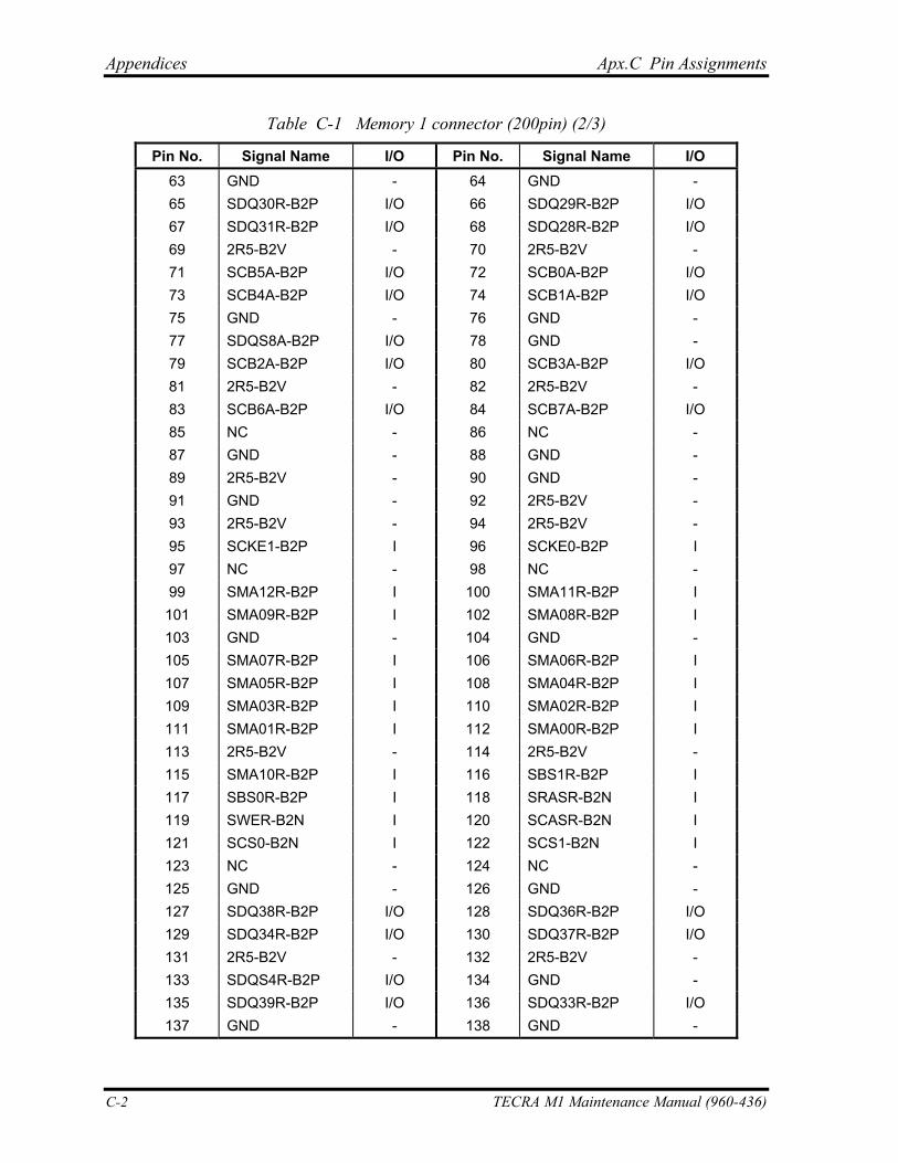
Appendices Apx.C Pin Assignments
Table C-1 Memory 1 connector (200pin) (2/3)
Pin No. Signal Name I/O Pin No. Signal Name I/O 63 GND - 64 GND - 65 SDQ30R-B2P I/O 66 SDQ29R-B2P I/O 67 SDQ31R-B2P I/O 68 SDQ28R-B2P I/O 69 2R5-B2V - 70 2R5-B2V - 71 SCB5A-B2P I/O 72 SCB0A-B2P I/O 73 SCB4A-B2P I/O 74 SCB1A-B2P I/O 75 GND - 76 GND - 77 SDQS8A-B2P I/O 78 GND - 79 SCB2A-B2P I/O 80 SCB3A-B2P I/O 81 2R5-B2V - 82 2R5-B2V - 83 SCB6A-B2P I/O 84 SCB7A-B2P I/O 85 NC - 86 NC - 87 GND - 88 GND - 89 2R5-B2V - 90 GND - 91 GND - 92 2R5-B2V - 93 2R5-B2V - 94 2R5-B2V - 95 SCKE1-B2P I 96 SCKE0-B2P I 97 NC - 98 NC - 99 SMA12R-B2P I 100 SMA11R-B2P I 101 SMA09R-B2P I 102 SMA08R-B2P I 103 GND - 104 GND - 105 SMA07R-B2P I 106 SMA06R-B2P I 107 SMA05R-B2P I 108 SMA04R-B2P I 109 SMA03R-B2P I 110 SMA02R-B2P I 111 SMA01R-B2P I 112 SMA00R-B2P I 113 2R5-B2V - 114 2R5-B2V - 115 SMA10R-B2P I 116 SBS1R-B2P I 117 SBS0R-B2P I 118 SRASR-B2N I 119 SWER-B2N I 120 SCASR-B2N I 121 SCS0-B2N I 122 SCS1-B2N I 123 NC - 124 NC - 125 GND - 126 GND - 127 SDQ38R-B2P I/O 128 SDQ36R-B2P I/O 129 SDQ34R-B2P I/O 130 SDQ37R-B2P I/O 131 2R5-B2V - 132 2R5-B2V - 133 SDQS4R-B2P I/O 134 GND - 135 SDQ39R-B2P I/O 136 SDQ33R-B2P I/O 137 GND - 138 GND -
C-2 TECRA M1 Maintenance Manual (960-436)
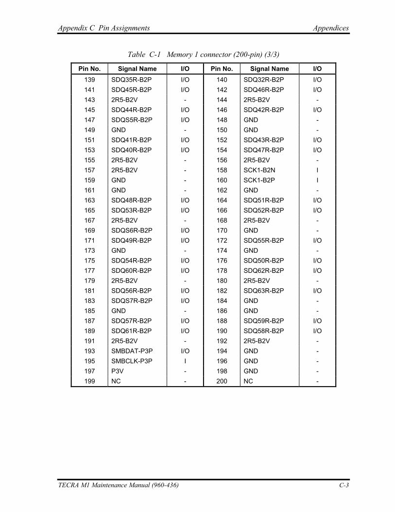
Appendix C Pin Assignments Appendices
Table C-1 Memory 1 connector (200-pin) (3/3)
Pin No. Signal Name I/O Pin No. Signal Name I/O 139 SDQ35R-B2P I/O 140 SDQ32R-B2P I/O 141 SDQ45R-B2P I/O 142 SDQ46R-B2P I/O 143 2R5-B2V - 144 2R5-B2V - 145 SDQ44R-B2P I/O 146 SDQ42R-B2P I/O 147 SDQS5R-B2P I/O 148 GND - 149 GND - 150 GND - 151 SDQ41R-B2P I/O 152 SDQ43R-B2P I/O 153 SDQ40R-B2P I/O 154 SDQ47R-B2P I/O 155 2R5-B2V - 156 2R5-B2V - 157 2R5-B2V - 158 SCK1-B2N I 159 GND - 160 SCK1-B2P I 161 GND - 162 GND - 163 SDQ48R-B2P I/O 164 SDQ51R-B2P I/O 165 SDQ53R-B2P I/O 166 SDQ52R-B2P I/O 167 2R5-B2V - 168 2R5-B2V - 169 SDQS6R-B2P I/O 170 GND - 171 SDQ49R-B2P I/O 172 SDQ55R-B2P I/O 173 GND - 174 GND - 175 SDQ54R-B2P I/O 176 SDQ50R-B2P I/O 177 SDQ60R-B2P I/O 178 SDQ62R-B2P I/O 179 2R5-B2V - 180 2R5-B2V - 181 SDQ56R-B2P I/O 182 SDQ63R-B2P I/O 183 SDQS7R-B2P I/O 184 GND - 185 GND - 186 GND - 187 SDQ57R-B2P I/O 188 SDQ59R-B2P I/O 189 SDQ61R-B2P I/O 190 SDQ58R-B2P I/O 191 2R5-B2V - 192 2R5-B2V - 193 SMBDAT-P3P I/O 194 GND - 195 SMBCLK-P3P I 196 GND - 197 P3V - 198 GND - 199 NC - 200 NC -
TECRA M1 Maintenance Manual (960-436) C-3
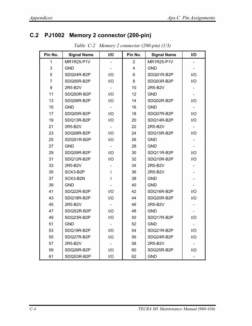
Appendices Apx.C Pin Assignments
C.2 PJ1002 Memory 2 connector (200-pin) Table C-2 Memory 2 connector (200-pin) (1/3)
Pin No. Signal Name I/O Pin No. Signal Name I/O 1 MR1R25-P1V - 2 MR1R25-P1V - 3 GND - 4 GND - 5 SDQ04R-B2P I/O 6 SDQ01R-B2P I/O 7 SDQ00R-B2P I/O 8 SDQ03R-B2P I/O 9 2R5-B2V - 10 2R5-B2V - 11 SDQS0R-B2P I/O 12 GND - 13 SDQ06R-B2P I/O 14 SDQ02R-B2P I/O 15 GND - 16 GND - 17 SDQ05R-B2P I/O 18 SDQ07R-B2P I/O 19 SDQ13R-B2P I/O 20 SDQ14R-B2P I/O 21 2R5-B2V - 22 2R5-B2V - 23 SDQ08R-B2P I/O 24 SDQ15R-B2P I/O 25 SDQS1R-B2P I/O 26 GND - 27 GND - 28 GND - 29 SDQ09R-B2P I/O 30 SDQ11R-B2P I/O 31 SDQ12R-B2P I/O 32 SDQ10R-B2P I/O 33 2R5-B2V - 34 2R5-B2V - 35 SCK3-B2P I 36 2R5-B2V - 37 SCK3-B2N I 38 GND - 39 GND - 40 GND - 41 SDQ22R-B2P I/O 42 SDQ16R-B2P I/O 43 SDQ18R-B2P I/O 44 SDQ20R-B2P I/O 45 2R5-B2V - 46 2R5-B2V - 47 SDQS2R-B2P I/O 48 GND - 49 SDQ23R-B2P I/O 50 SDQ17R-B2P I/O 51 GND - 52 GND - 53 SDQ19R-B2P I/O 54 SDQ21R-B2P I/O 55 SDQ27R-B2P I/O 56 SDQ24R-B2P I/O 57 2R5-B2V - 58 2R5-B2V - 59 SDQ26R-B2P I/O 60 SDQ25R-B2P I/O 61 SDQS3R-B2P I/O 62 GND -
C-4 TECRA M1 Maintenance Manual (960-436)
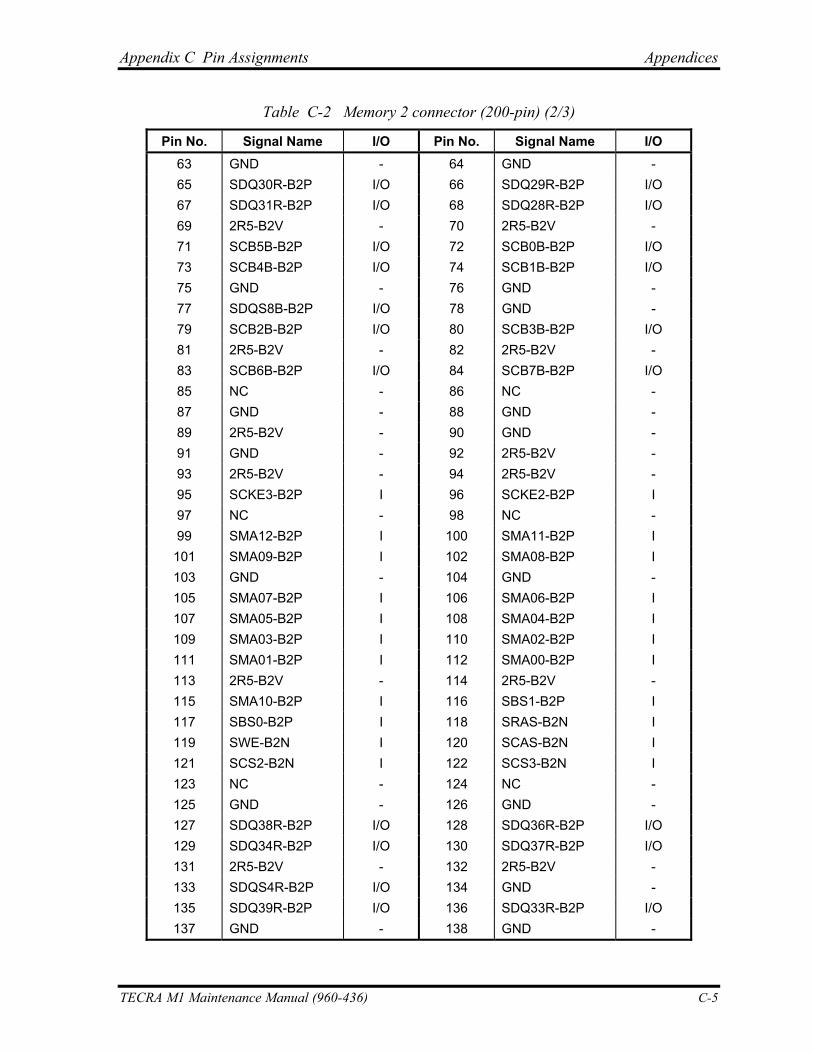
Appendix C Pin Assignments Appendices
Table C-2 Memory 2 connector (200-pin) (2/3)
Pin No. Signal Name I/O Pin No. Signal Name I/O 63 GND - 64 GND - 65 SDQ30R-B2P I/O 66 SDQ29R-B2P I/O 67 SDQ31R-B2P I/O 68 SDQ28R-B2P I/O 69 2R5-B2V - 70 2R5-B2V - 71 SCB5B-B2P I/O 72 SCB0B-B2P I/O 73 SCB4B-B2P I/O 74 SCB1B-B2P I/O 75 GND - 76 GND - 77 SDQS8B-B2P I/O 78 GND - 79 SCB2B-B2P I/O 80 SCB3B-B2P I/O 81 2R5-B2V - 82 2R5-B2V - 83 SCB6B-B2P I/O 84 SCB7B-B2P I/O 85 NC - 86 NC - 87 GND - 88 GND - 89 2R5-B2V - 90 GND - 91 GND - 92 2R5-B2V - 93 2R5-B2V - 94 2R5-B2V - 95 SCKE3-B2P I 96 SCKE2-B2P I 97 NC - 98 NC - 99 SMA12-B2P I 100 SMA11-B2P I 101 SMA09-B2P I 102 SMA08-B2P I 103 GND - 104 GND - 105 SMA07-B2P I 106 SMA06-B2P I 107 SMA05-B2P I 108 SMA04-B2P I 109 SMA03-B2P I 110 SMA02-B2P I 111 SMA01-B2P I 112 SMA00-B2P I 113 2R5-B2V - 114 2R5-B2V - 115 SMA10-B2P I 116 SBS1-B2P I 117 SBS0-B2P I 118 SRAS-B2N I 119 SWE-B2N I 120 SCAS-B2N I 121 SCS2-B2N I 122 SCS3-B2N I 123 NC - 124 NC - 125 GND - 126 GND - 127 SDQ38R-B2P I/O 128 SDQ36R-B2P I/O 129 SDQ34R-B2P I/O 130 SDQ37R-B2P I/O 131 2R5-B2V - 132 2R5-B2V - 133 SDQS4R-B2P I/O 134 GND - 135 SDQ39R-B2P I/O 136 SDQ33R-B2P I/O 137 GND - 138 GND -
TECRA M1 Maintenance Manual (960-436) C-5
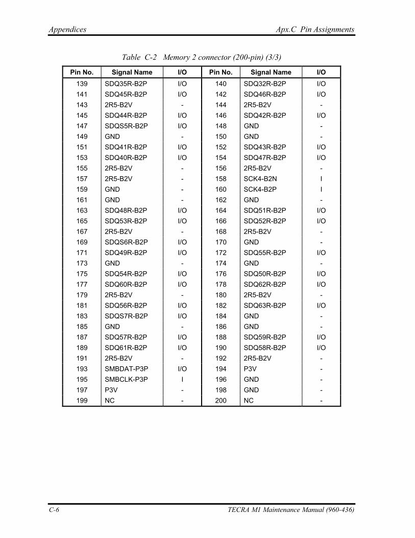
Appendices Apx.C Pin Assignments
Table C-2 Memory 2 connector (200-pin) (3/3)
Pin No. Signal Name I/O Pin No. Signal Name I/O 139 SDQ35R-B2P I/O 140 SDQ32R-B2P I/O 141 SDQ45R-B2P I/O 142 SDQ46R-B2P I/O 143 2R5-B2V - 144 2R5-B2V - 145 SDQ44R-B2P I/O 146 SDQ42R-B2P I/O 147 SDQS5R-B2P I/O 148 GND - 149 GND - 150 GND - 151 SDQ41R-B2P I/O 152 SDQ43R-B2P I/O 153 SDQ40R-B2P I/O 154 SDQ47R-B2P I/O 155 2R5-B2V - 156 2R5-B2V - 157 2R5-B2V - 158 SCK4-B2N I 159 GND - 160 SCK4-B2P I 161 GND - 162 GND - 163 SDQ48R-B2P I/O 164 SDQ51R-B2P I/O 165 SDQ53R-B2P I/O 166 SDQ52R-B2P I/O 167 2R5-B2V - 168 2R5-B2V - 169 SDQS6R-B2P I/O 170 GND - 171 SDQ49R-B2P I/O 172 SDQ55R-B2P I/O 173 GND - 174 GND - 175 SDQ54R-B2P I/O 176 SDQ50R-B2P I/O 177 SDQ60R-B2P I/O 178 SDQ62R-B2P I/O 179 2R5-B2V - 180 2R5-B2V - 181 SDQ56R-B2P I/O 182 SDQ63R-B2P I/O 183 SDQS7R-B2P I/O 184 GND - 185 GND - 186 GND - 187 SDQ57R-B2P I/O 188 SDQ59R-B2P I/O 189 SDQ61R-B2P I/O 190 SDQ58R-B2P I/O 191 2R5-B2V - 192 2R5-B2V - 193 SMBDAT-P3P I/O 194 P3V - 195 SMBCLK-P3P I 196 GND - 197 P3V - 198 GND - 199 NC - 200 NC -
C-6 TECRA M1 Maintenance Manual (960-436)
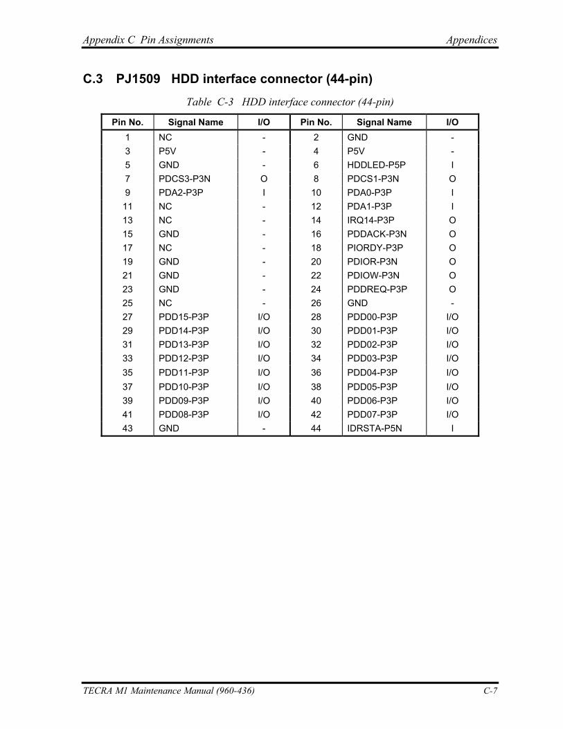
Appendix C Pin Assignments Appendices
C.3 PJ1509 HDD interface connector (44-pin) Table C-3 HDD interface connector (44-pin)
Pin No. Signal Name I/O Pin No. Signal Name I/O 1 NC - 2 GND - 3 P5V - 4 P5V - 5 GND - 6 HDDLED-P5P I 7 PDCS3-P3N O 8 PDCS1-P3N O 9 PDA2-P3P I 10 PDA0-P3P I
11 NC - 12 PDA1-P3P I 13 NC - 14 IRQ14-P3P O 15 GND - 16 PDDACK-P3N O 17 NC - 18 PIORDY-P3P O 19 GND - 20 PDIOR-P3N O 21 GND - 22 PDIOW-P3N O 23 GND - 24 PDDREQ-P3P O 25 NC - 26 GND - 27 PDD15-P3P I/O 28 PDD00-P3P I/O 29 PDD14-P3P I/O 30 PDD01-P3P I/O 31 PDD13-P3P I/O 32 PDD02-P3P I/O 33 PDD12-P3P I/O 34 PDD03-P3P I/O 35 PDD11-P3P I/O 36 PDD04-P3P I/O 37 PDD10-P3P I/O 38 PDD05-P3P I/O 39 PDD09-P3P I/O 40 PDD06-P3P I/O 41 PDD08-P3P I/O 42 PDD07-P3P I/O 43 GND - 44 IDRSTA-P5N I
TECRA M1 Maintenance Manual (960-436) C-7
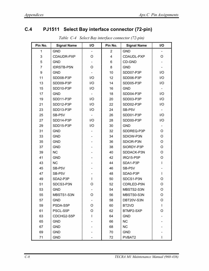
Appendices Apx.C Pin Assignments
C.4 PJ1511 Select Bay interface connector (72-pin) Table C-4 Select Bay interface connector (72-pin)
Pin No. Signal Name I/O Pin No. Signal Name I/O 1 GND - 2 GND - 3 CDAUDR-PXP O 4 CDAUDL-PXP O 5 GND - 6 CD-GND - 7 IDRSTB-P5N O 8 GND - 9 GND - 10 SDD07-P3P I/O
11 SDD08-P3P I/O 12 SDD06-P3P I/O 13 SDD09-P3P I/O 14 SDD05-P3P I/O 15 SDD10-P3P I/O 16 GND - 17 GND - 18 SDD04-P3P I/O 19 SDD11-P3P I/O 20 SDD03-P3P I/O 21 SDD12-P3P I/O 22 SDD02-P3P I/O 23 SDD13-P3P I/O 24 SB-P5V - 25 SB-P5V - 26 SDD01-P3P I/O 27 SDD14-P3P I/O 28 SDD00-P3P I/O 29 SDD15-P3P I/O 30 GND - 31 GND - 32 SDDREQ-P3P O 33 GND - 34 SDIOW-P3N O 35 GND - 36 SDIOR-P3N O 37 GND - 38 SIORDY-P3P O 39 NC - 40 SDDACK-P3N O 41 GND - 42 IRQ15-P5P O 43 NC - 44 SDA1-P3P I 45 SB-P5V - 46 SB-P5V - 47 SB-P5V - 48 SDA0-P3P I 49 SDA2-P3P I 50 SDCS1-P3N O 51 SDCS3-P3N O 52 CDRLED-P5N O 53 GND - 54 MBSTS2-S3N O 55 MBSTS1-S3N O 56 MBSTS0-S3N O 57 GND - 58 DBT20V-S3N O 59 PSDA-S5P O 60 BT2VD I 61 PSCL-S5P O 62 BTMP2-SXP O 63 CDCHG2-S5P I 64 GND - 65 GND - 66 NC - 67 GND - 68 NC - 69 GND - 70 GND - 71 GND - 72 PVBAT2 I
C-8 TECRA M1 Maintenance Manual (960-436)
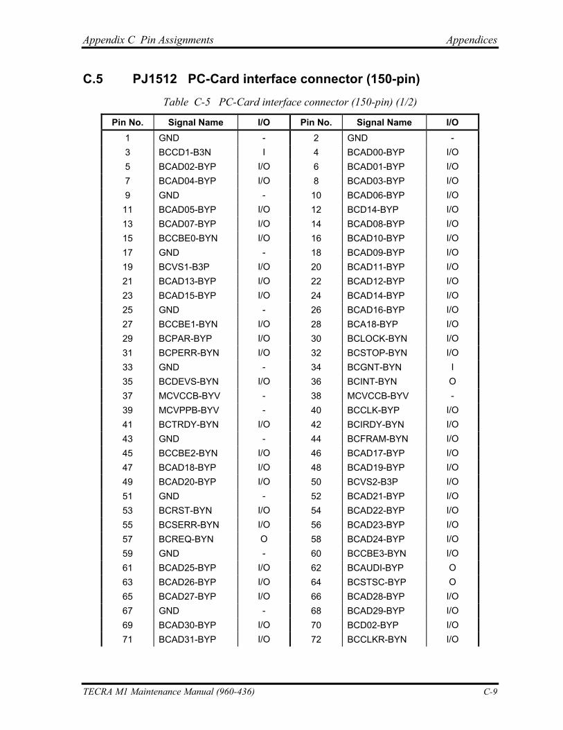
Appendix C Pin Assignments Appendices
C.5 PJ1512 PC-Card interface connector (150-pin) Table C-5 PC-Card interface connector (150-pin) (1/2)
Pin No. Signal Name I/O Pin No. Signal Name I/O 1 GND - 2 GND - 3 BCCD1-B3N I 4 BCAD00-BYP I/O 5 BCAD02-BYP I/O 6 BCAD01-BYP I/O 7 BCAD04-BYP I/O 8 BCAD03-BYP I/O 9 GND - 10 BCAD06-BYP I/O
11 BCAD05-BYP I/O 12 BCD14-BYP I/O 13 BCAD07-BYP I/O 14 BCAD08-BYP I/O 15 BCCBE0-BYN I/O 16 BCAD10-BYP I/O 17 GND - 18 BCAD09-BYP I/O 19 BCVS1-B3P I/O 20 BCAD11-BYP I/O 21 BCAD13-BYP I/O 22 BCAD12-BYP I/O 23 BCAD15-BYP I/O 24 BCAD14-BYP I/O 25 GND - 26 BCAD16-BYP I/O 27 BCCBE1-BYN I/O 28 BCA18-BYP I/O 29 BCPAR-BYP I/O 30 BCLOCK-BYN I/O 31 BCPERR-BYN I/O 32 BCSTOP-BYN I/O 33 GND - 34 BCGNT-BYN I 35 BCDEVS-BYN I/O 36 BCINT-BYN O 37 MCVCCB-BYV - 38 MCVCCB-BYV - 39 MCVPPB-BYV - 40 BCCLK-BYP I/O 41 BCTRDY-BYN I/O 42 BCIRDY-BYN I/O 43 GND - 44 BCFRAM-BYN I/O 45 BCCBE2-BYN I/O 46 BCAD17-BYP I/O 47 BCAD18-BYP I/O 48 BCAD19-BYP I/O 49 BCAD20-BYP I/O 50 BCVS2-B3P I/O 51 GND - 52 BCAD21-BYP I/O 53 BCRST-BYN I/O 54 BCAD22-BYP I/O 55 BCSERR-BYN I/O 56 BCAD23-BYP I/O 57 BCREQ-BYN O 58 BCAD24-BYP I/O 59 GND - 60 BCCBE3-BYN I/O 61 BCAD25-BYP I/O 62 BCAUDI-BYP O 63 BCAD26-BYP I/O 64 BCSTSC-BYP O 65 BCAD27-BYP I/O 66 BCAD28-BYP I/O 67 GND - 68 BCAD29-BYP I/O 69 BCAD30-BYP I/O 70 BCD02-BYP I/O 71 BCAD31-BYP I/O 72 BCCLKR-BYN I/O
TECRA M1 Maintenance Manual (960-436) C-9
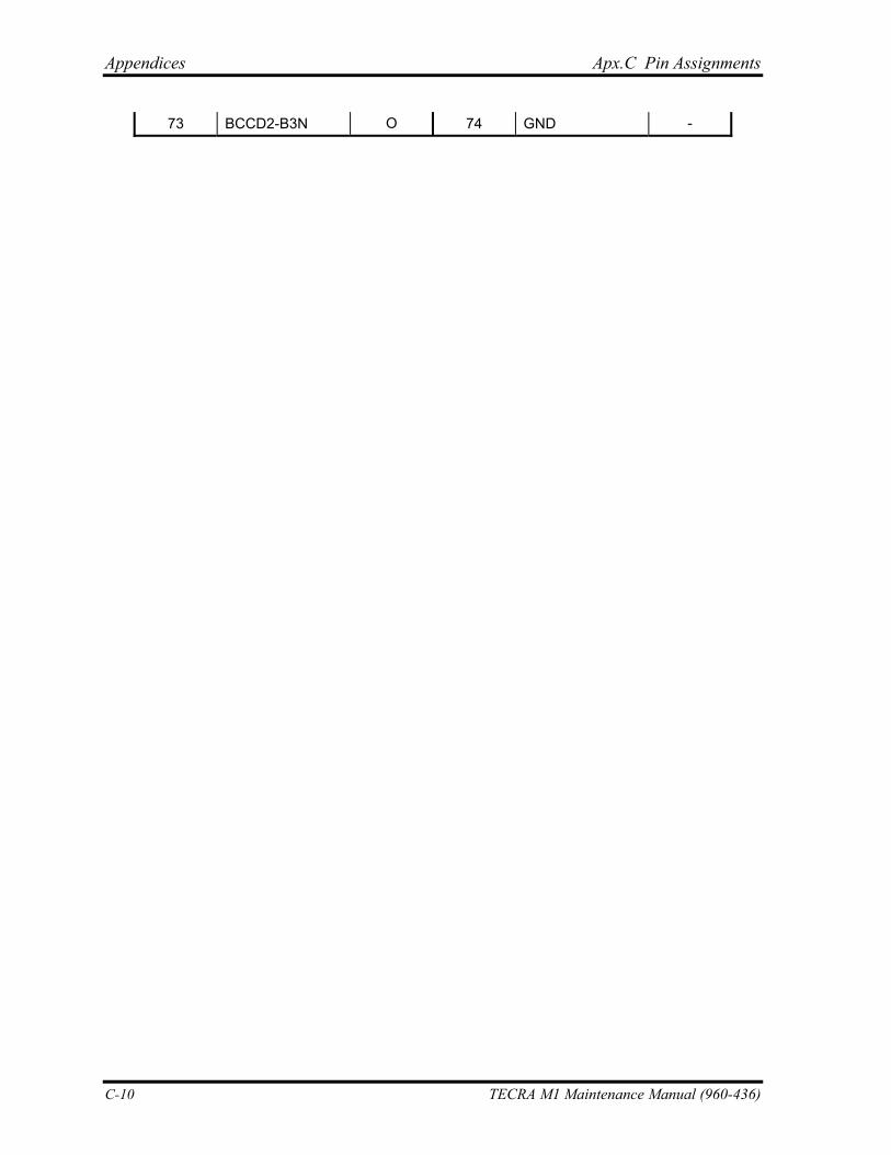
Appendices Apx.C Pin Assignments
73 BCCD2-B3N O 74 GND -
C-10 TECRA M1 Maintenance Manual (960-436)
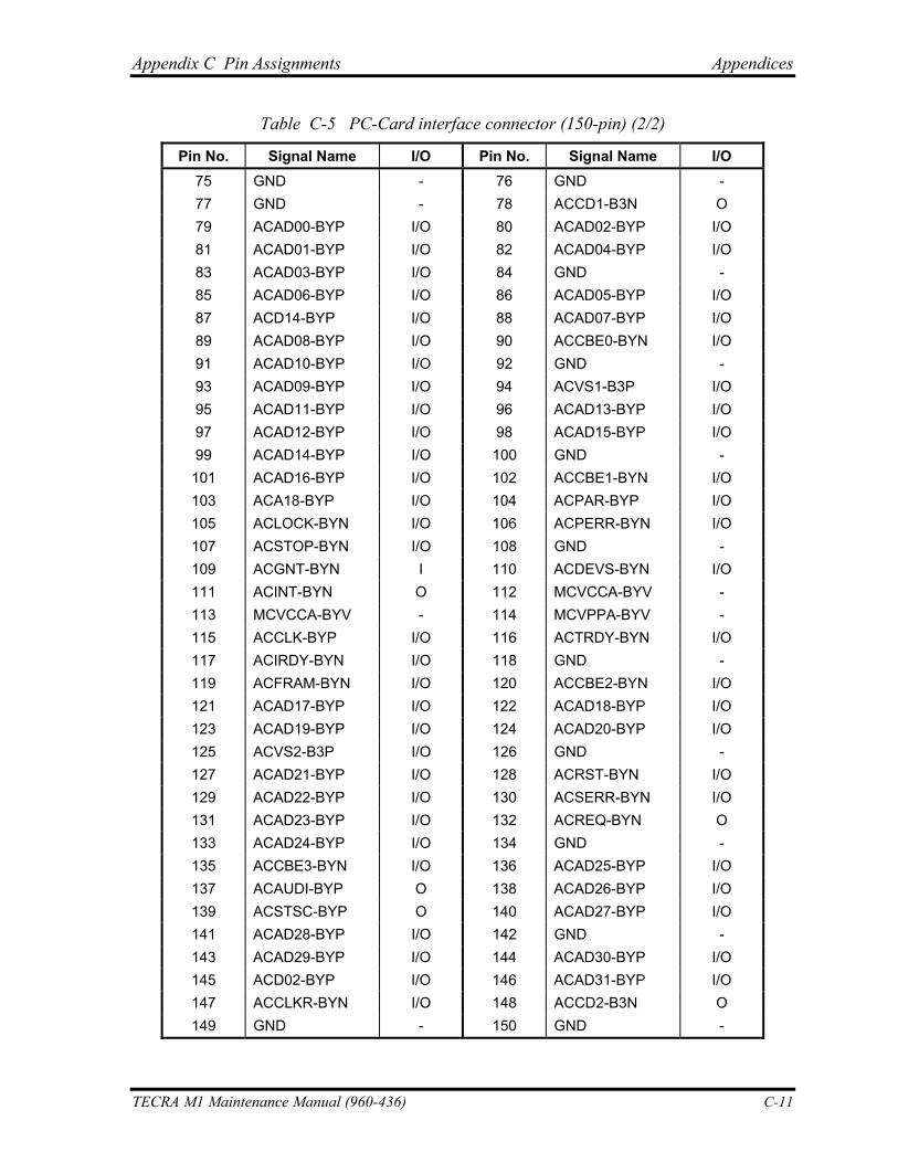
Appendix C Pin Assignments Appendices
Table C-5 PC-Card interface connector (150-pin) (2/2)
Pin No. Signal Name I/O Pin No. Signal Name I/O 75 GND - 76 GND - 77 GND - 78 ACCD1-B3N O 79 ACAD00-BYP I/O 80 ACAD02-BYP I/O 81 ACAD01-BYP I/O 82 ACAD04-BYP I/O 83 ACAD03-BYP I/O 84 GND - 85 ACAD06-BYP I/O 86 ACAD05-BYP I/O 87 ACD14-BYP I/O 88 ACAD07-BYP I/O 89 ACAD08-BYP I/O 90 ACCBE0-BYN I/O 91 ACAD10-BYP I/O 92 GND - 93 ACAD09-BYP I/O 94 ACVS1-B3P I/O 95 ACAD11-BYP I/O 96 ACAD13-BYP I/O 97 ACAD12-BYP I/O 98 ACAD15-BYP I/O 99 ACAD14-BYP I/O 100 GND - 101 ACAD16-BYP I/O 102 ACCBE1-BYN I/O 103 ACA18-BYP I/O 104 ACPAR-BYP I/O 105 ACLOCK-BYN I/O 106 ACPERR-BYN I/O 107 ACSTOP-BYN I/O 108 GND - 109 ACGNT-BYN I 110 ACDEVS-BYN I/O 111 ACINT-BYN O 112 MCVCCA-BYV - 113 MCVCCA-BYV - 114 MCVPPA-BYV - 115 ACCLK-BYP I/O 116 ACTRDY-BYN I/O 117 ACIRDY-BYN I/O 118 GND - 119 ACFRAM-BYN I/O 120 ACCBE2-BYN I/O 121 ACAD17-BYP I/O 122 ACAD18-BYP I/O 123 ACAD19-BYP I/O 124 ACAD20-BYP I/O 125 ACVS2-B3P I/O 126 GND - 127 ACAD21-BYP I/O 128 ACRST-BYN I/O 129 ACAD22-BYP I/O 130 ACSERR-BYN I/O 131 ACAD23-BYP I/O 132 ACREQ-BYN O 133 ACAD24-BYP I/O 134 GND - 135 ACCBE3-BYN I/O 136 ACAD25-BYP I/O 137 ACAUDI-BYP O 138 ACAD26-BYP I/O 139 ACSTSC-BYP O 140 ACAD27-BYP I/O 141 ACAD28-BYP I/O 142 GND - 143 ACAD29-BYP I/O 144 ACAD30-BYP I/O 145 ACD02-BYP I/O 146 ACAD31-BYP I/O 147 ACCLKR-BYN I/O 148 ACCD2-B3N O 149 GND - 150 GND -
TECRA M1 Maintenance Manual (960-436) C-11
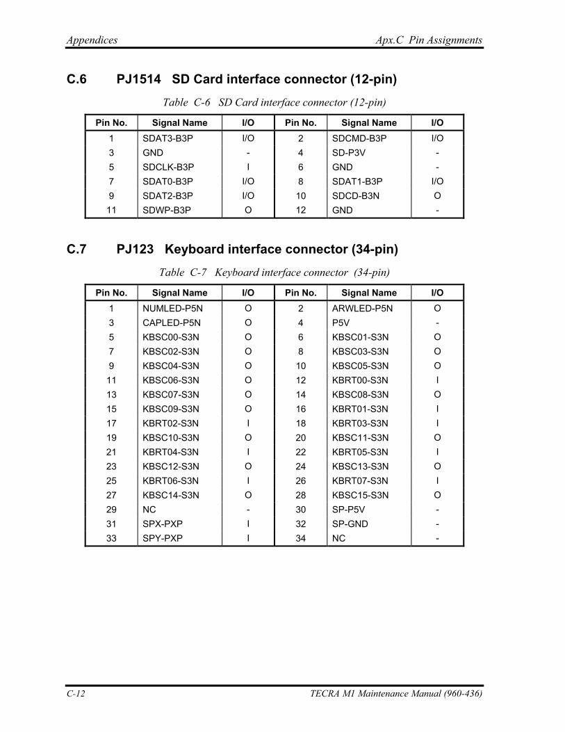
Appendices Apx.C Pin Assignments
C.6 PJ1514 SD Card interface connector (12-pin) Table C-6 SD Card interface connector (12-pin)
Pin No. Signal Name Pin No. Signal Name I/O 1 SDAT3-B3P 2 SDCMD-B3P I/O 3 GND 4 SD-P3V - 5 SDCLK-B3P 6 GND - 7 SDAT0-B3P 8 SDAT1-B3P I/O 9 SDAT2-B3P 10 SDCD-B3N O
11
I/O I/O - I
I/O I/O
SDWP-B3P O 12 GND -
C.7 PJ123 Keyboard interface connector (34-pin) Table C-7 Keyboard interface connector (34-pin)
Pin No. Signal Name I/O Pin No. Signal Name I/O 1 NUMLED-P5N O 2 ARWLED-P5N O 3 CAPLED-P5N O 4 P5V -
KBSC00-S3N O 6 KBSC01-S3N O 7 KBSC02-S3N O 8 KBSC03-S3N O 9 KBSC04-S3N O 10 KBSC05-S3N O
11 KBSC06-S3N O 12 KBRT00-S3N I 13 KBSC07-S3N O 14 KBSC08-S3N O 15 KBSC09-S3N O 16 KBRT01-S3N I 17 KBRT02-S3N I 18 KBRT03-S3N I 19 KBSC10-S3N O 20 KBSC11-S3N O 21 KBRT04-S3N I 22 KBRT05-S3N I 23 KBSC12-S3N O 24 KBSC13-S3N O 25 KBRT06-S3N I 26 KBRT07-S3N I 27 KBSC14-S3N O 28 KBSC15-S3N O 29 NC - 30 SP-P5V - 31 SPX-PXP I 32 SP-GND - 33 SPY-PXP I 34 NC -
5
C-12 TECRA M1 Maintenance Manual (960-436)
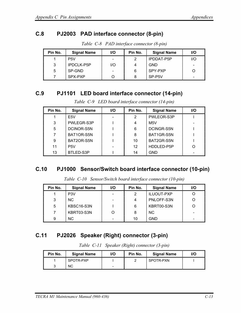
Appendix C Pin Assignments Appendices
C.8 PJ2003 PAD interface connector (8-pin) Table C-8 PAD interface connector (8-pin)
Pin No. Signal Name I/O Pin No. Signal Name I/O 1 P5V - 2 IPDDAT-P5P I/O 3 IPDCLK-P5P I/O 4 GND - 5 SP-GND - 6 SPY-PXP O 7 SPX-PXP O 8 SP-P5V -
C.9 PJ1101 LED board interface connector (14-pin) Table C-9 LED board interface connector (14-pin)
Pin No. Signal Name I/O Pin No. Signal Name I/O 1 E5V - 2 PWLEOR-S3P I 3 PWLEGR-S3P I 4 M5V - 5 DCINOR-S5N I 6 DCINGR-S5N I 7 BAT1OR-S5N I 8 BAT1GR-S5N I 9 BAT2OR-S5N I 10 BAT2GR-S5N I
11 P5V - 12 HDDLED-P5P O 13 BTLED-S3P I 14 GND -
C.10 PJ1000 Sensor/Switch board interface connector (10-pin) Table C-10 Sensor/Switch board interface connector (10-pin)
Pin No. Signal Name I/O Pin No. Signal Name I/O1 P3V - 2 ILUOUT-PXP O 3 NC - 4 PNLOFF-S3N O 5 KBSC16-S3N I 6 KBRT00-S3N O 7 KBRT03-S3N O 8 NC - 9 NC - 10 GND -
C.11 PJ2026 Speaker (Right) connector (3-pin) Table C-11 Speaker (Right) connector (3-pin)
Pin No. Signal Name I/O Pin No. Signal Name I/O 1 SPOTR-PXP I 2 SPOTR-PXN I 3 NC -
TECRA M1 Maintenance Manual (960-436) C-13
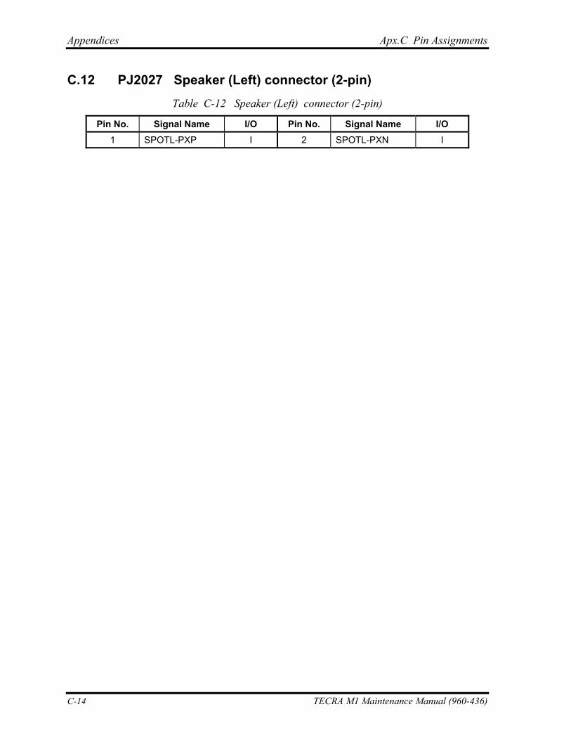
Appendices Apx.C Pin Assignments
C.12 PJ2027 Speaker (Left) connector (2-pin) Table C-12 Speaker (Left) connector (2-pin)
Pin No. Signal Name I/O Pin No. Signal Name I/O 1 SPOTL-PXP I 2 SPOTL-PXN I
C-14 TECRA M1 Maintenance Manual (960-436)
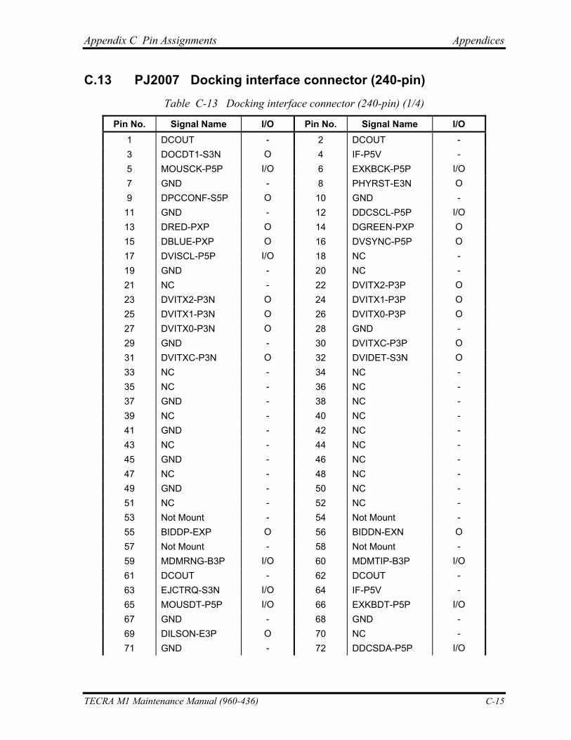
Appendix C Pin Assignments Appendices
C.13 PJ2007 Docking interface connector (240-pin) Table C-13 Docking interface connector (240-pin) (1/4)
Pin No. Signal Name I/O Pin No. Signal Name I/O 1 DCOUT - 2 DCOUT - 3 DOCDT1-S3N O 4 IF-P5V - 5 MOUSCK-P5P I/O 6 EXKBCK-P5P I/O 7 GND - 8 PHYRST-E3N O 9 DPCCONF-S5P O 10 GND -
11 GND - 12 DDCSCL-P5P I/O 13 DRED-PXP O 14 DGREEN-PXP O 15 DBLUE-PXP O 16 DVSYNC-P5P O 17 DVISCL-P5P I/O 18 NC - 19 GND - 20 NC - 21 NC - 22 DVITX2-P3P O 23 DVITX2-P3N O 24 DVITX1-P3P O 25 DVITX1-P3N O 26 DVITX0-P3P O 27 DVITX0-P3N O 28 GND - 29 GND - 30 DVITXC-P3P O 31 DVITXC-P3N O 32 DVIDET-S3N O 33 NC - 34 NC - 35 NC - 36 NC - 37 GND - 38 NC - 39 NC - 40 NC - 41 GND - 42 NC - 43 NC - 44 NC - 45 GND - 46 NC - 47 NC - 48 NC - 49 GND - 50 NC - 51 NC - 52 NC - 53 Not Mount - 54 Not Mount - 55 BIDDP-EXP O 56 BIDDN-EXN O 57 Not Mount - 58 Not Mount - 59 MDMRNG-B3P I/O 60 MDMTIP-B3P I/O 61 DCOUT - 62 DCOUT - 63 EJCTRQ-S3N I/O 64 IF-P5V - 65 MOUSDT-P5P I/O 66 EXKBDT-P5P I/O 67 GND - 68 GND - 69 DILSON-E3P O 70 NC - 71 GND - 72 DDCSDA-P5P I/O
TECRA M1 Maintenance Manual (960-436) C-15
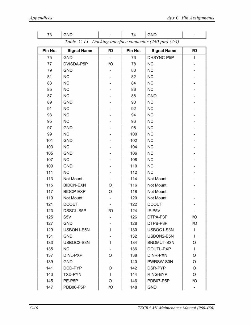
Appendices Apx.C Pin Assignments
73 GND - 74 GND -
Table C-13 Docking interface connector (240-pin) (2/4)
Pin No. Signal Name I/O Pin No. Signal Name I/O 75 GND - 76 DHSYNC-P5P I 77 DVISDA-P5P I/O 78 NC - 79 GND - 80 NC - 81 NC - 82 NC - 83 NC - 84 NC - 85 NC - 86 NC - 87 NC - 88 GND - 89 GND - 90 NC - 91 NC - 92 NC - 93 NC - 94 NC - 95 NC - 96 NC - 97 GND - 98 NC - 99 NC - 100 NC - 101 GND - 102 NC - 103 NC - 104 NC - 105 GND - 106 NC - 107 NC - 108 NC - 109 GND - 110 NC - 111 NC - 112 NC - 113 Not Mount - 114 Not Mount - 115 BIDCN-EXN O 116 Not Mount - 117 BIDCP-EXP O 118 Not Mount - 119 Not Mount - 120 Not Mount - 121 DCOUT - 122 DCOUT - 123 DSSCL-S5P I/O 124 IF-P5V - 125 S5V - 126 DTPA-P3P I/O 127 GND - 128 DTPB-P3P I/O 129 USBON1-E5N I 130 USBOC1-S3N I 131 GND - 132 USBON2-E5N I 133 USBOC2-S3N I 134 SNDMUT-S3N O 135 NC - 136 DOUTL-PXP I 137 DINL-PXP O 138 DINR-PXN O 139 GND - 140 PWRSW-S3N O 141 DCD-PYP O 142 DSR-PYP O 143 TXD-PYN I 144 RING-BYP O 145 PE-P5P O 146 PDB07-P5P I/O 147 PDB06-P5P I/O 148 GND -
C-16 TECRA M1 Maintenance Manual (960-436)
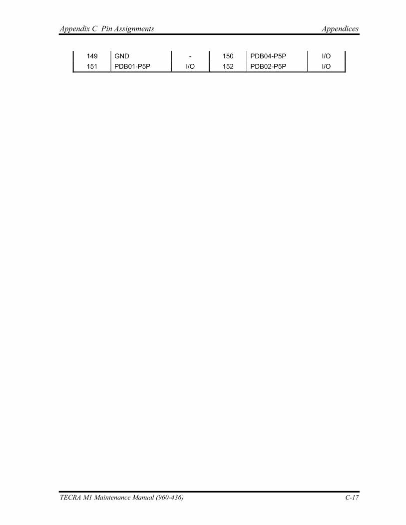
Appendix C Pin Assignments Appendices
149 GND - 150 PDB04-P5P I/O 151 PDB01-P5P I/O 152 PDB02-P5P I/O
TECRA M1 Maintenance Manual (960-436) C-17
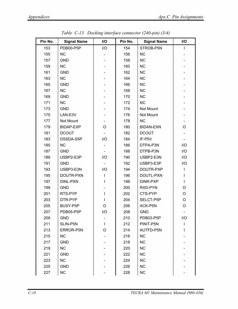
Appendices Apx.C Pin Assignments
Table C-13 Docking interface connector (240-pin) (3/4)
Pin No. Signal Name I/O Pin No. Signal Name I/O 153 PDB00-P5P I/O 154 STROB-P5N I 155 NC - 156 NC - 157 GND - 158 NC - 159 NC - 160 NC - 161 GND - 162 NC - 163 NC - 164 NC - 165 GND - 166 NC - 167 NC - 168 NC - 169 GND - 170 NC - 171 NC - 172 NC - 173 GND - 174 Not Mount - 175 LAN-E3V - 176 Not Mount - 177 Not Mount - 178 NC - 179 BIDAP-EXP O 180 BIDAN-EXN O 181 DCOUT - 182 DCOUT - 183 DSSDA-S5P I/O 184 IF-P5V - 185 NC - 186 DTPA-P3N I/O 187 GND - 188 DTPB-P3N I/O 189 USBP2-E3P I/O 190 USBP2-E3N I/O 191 GND - 192 USBP3-E3P I/O 193 USBP3-E3N I/O 194 DOUTR-PXP I 195 DOUTR-PXN I 196 DOUTL-PXN I 197 DINL-PXN I 198 DINR-PXP I 199 GND - 200 RXD-PYN O 201 RTS-PYP I 202 CTS-PYP O 203 DTR-PYP I 204 SELCT-P5P O 205 BUSY-P5P O 206 ACK-P5N O 207 PDB05-P5P I/O 208 GND - 209 GND - 210 PDB03-P5P I/O 211 SLIN-P5N I 212 PINIT-P5N I 213 ERROR-P5N O 214 AUTFD-P5N I 215 NC - 216 NC - 217 GND - 218 NC - 219 NC - 220 NC - 221 GND - 222 NC - 223 NC - 224 NC - 225 GND - 226 NC - 227 NC - 228 NC -
C-18 TECRA M1 Maintenance Manual (960-436)
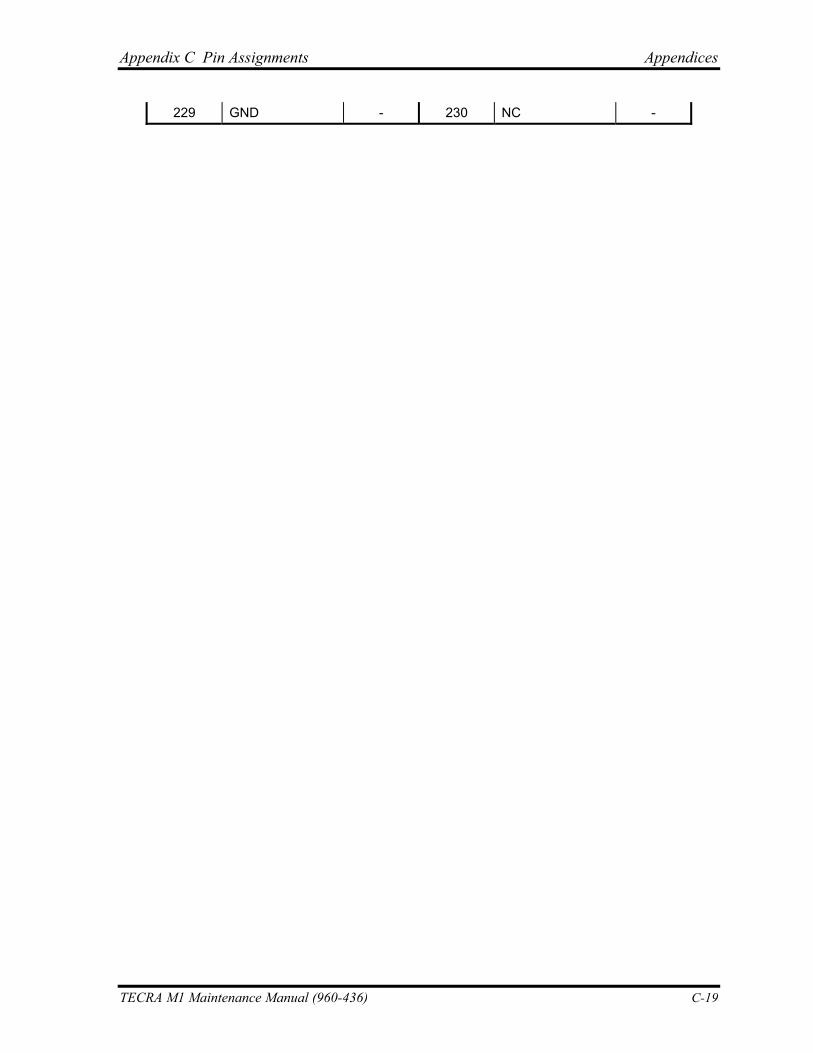
Appendix C Pin Assignments Appendices
229 GND - 230 NC -
TECRA M1 Maintenance Manual (960-436) C-19
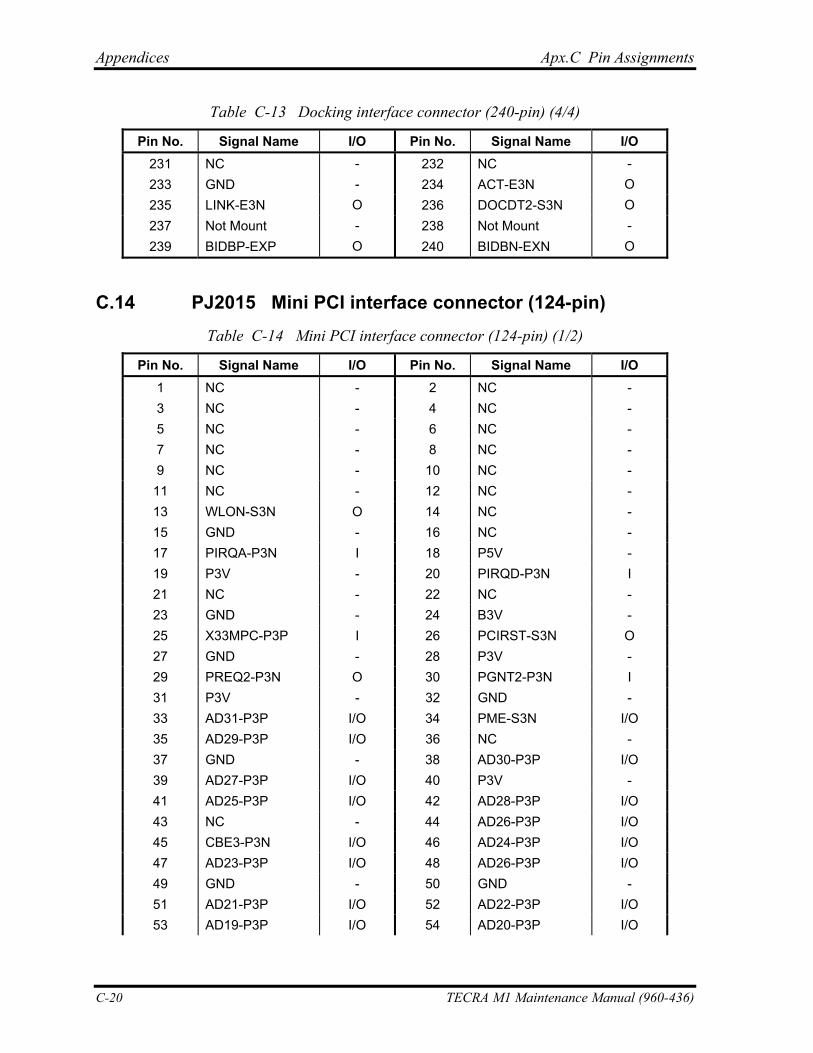
Appendices Apx.C Pin Assignments
Table C-13 Docking interface connector (240-pin) (4/4)
Pin No. Signal Name I/O Pin No. Signal Name I/O 231 NC - 232 NC - 233 GND - 234 ACT-E3N O 235 LINK-E3N O 236 DOCDT2-S3N O 237 Not Mount - 238 Not Mount - 239 BIDBP-EXP O 240 BIDBN-EXN O
C.14 PJ2015 Mini PCI interface connector (124-pin) Table C-14 Mini PCI interface connector (124-pin) (1/2)
Pin No. Signal Name I/O Pin No. Signal Name I/O 1 NC - 2 NC - 3 NC - 4 NC - 5 NC - 6 NC - 7 NC - 8 NC - 9 NC - 10 NC -
11 NC - 12 NC - 13 WLON-S3N O 14 NC - 15 GND - 16 NC - 17 PIRQA-P3N I 18 P5V - 19 P3V - 20 PIRQD-P3N I 21 NC - 22 NC - 23 GND - 24 B3V - 25 X33MPC-P3P I 26 PCIRST-S3N O 27 GND - 28 P3V - 29 PREQ2-P3N O 30 PGNT2-P3N I 31 P3V - 32 GND - 33 AD31-P3P I/O 34 PME-S3N I/O 35 AD29-P3P I/O 36 NC - 37 GND - 38 AD30-P3P I/O 39 AD27-P3P I/O 40 P3V - 41 AD25-P3P I/O 42 AD28-P3P I/O 43 NC - 44 AD26-P3P I/O 45 CBE3-P3N I/O 46 AD24-P3P I/O 47 AD23-P3P I/O 48 AD26-P3P I/O 49 GND - 50 GND - 51 AD21-P3P I/O 52 AD22-P3P I/O 53 AD19-P3P I/O 54 AD20-P3P I/O
C-20 TECRA M1 Maintenance Manual (960-436)
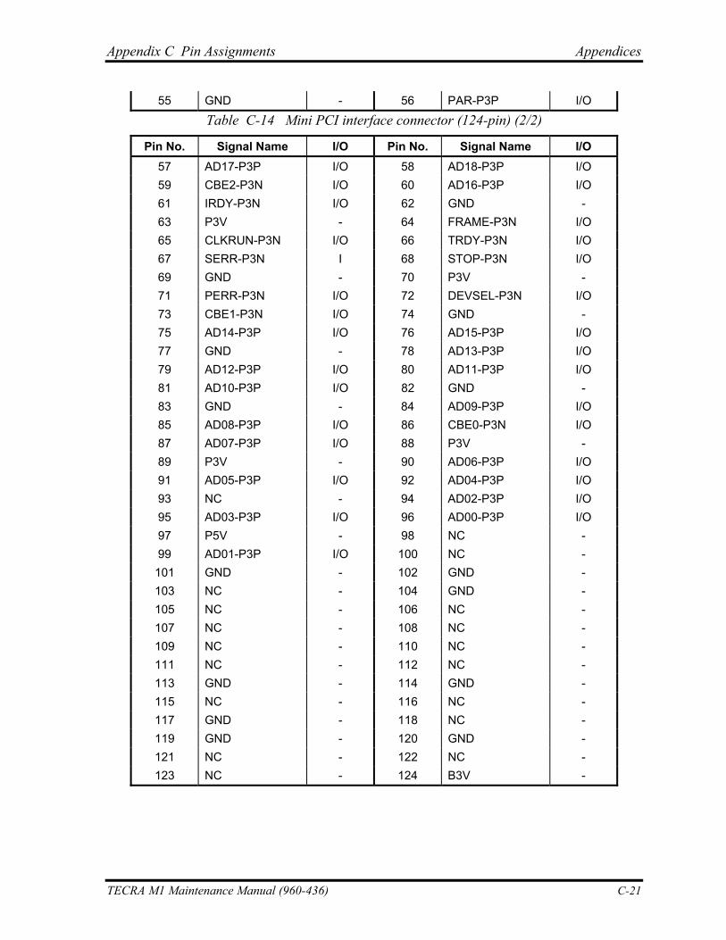
Appendix C Pin Assignments Appendices
55 GND - 56 PAR-P3P I/O Table C-14 Mini PCI interface connector (124-pin) (2/2)
Pin No. Signal Name I/O Pin No. Signal Name I/O 57 AD17-P3P I/O 58 AD18-P3P I/O 59 CBE2-P3N I/O 60 AD16-P3P I/O 61 IRDY-P3N I/O 62 GND - 63 P3V - 64 FRAME-P3N I/O 65 CLKRUN-P3N I/O 66 TRDY-P3N I/O 67 SERR-P3N I 68 STOP-P3N I/O 69 GND - 70 P3V - 71 PERR-P3N I/O 72 DEVSEL-P3N I/O 73 CBE1-P3N I/O 74 GND - 75 AD14-P3P I/O 76 AD15-P3P I/O 77 GND - 78 AD13-P3P I/O 79 AD12-P3P I/O 80 AD11-P3P I/O 81 AD10-P3P I/O 82 GND - 83 GND - 84 AD09-P3P I/O 85 AD08-P3P I/O 86 CBE0-P3N I/O 87 AD07-P3P I/O 88 P3V - 89 P3V - 90 AD06-P3P I/O 91 AD05-P3P I/O 92 AD04-P3P I/O 93 NC - 94 AD02-P3P I/O 95 AD03-P3P I/O 96 AD00-P3P I/O 97 P5V - 98 NC - 99 AD01-P3P I/O 100 NC - 101 GND - 102 GND - 103 NC - 104 GND - 105 NC - 106 NC - 107 NC - 108 NC - 109 NC - 110 NC - 111 NC - 112 NC - 113 GND - 114 GND - 115 NC - 116 NC - 117 GND - 118 NC - 119 GND - 120 GND - 121 NC - 122 NC - 123 NC - 124 B3V -
TECRA M1 Maintenance Manual (960-436) C-21
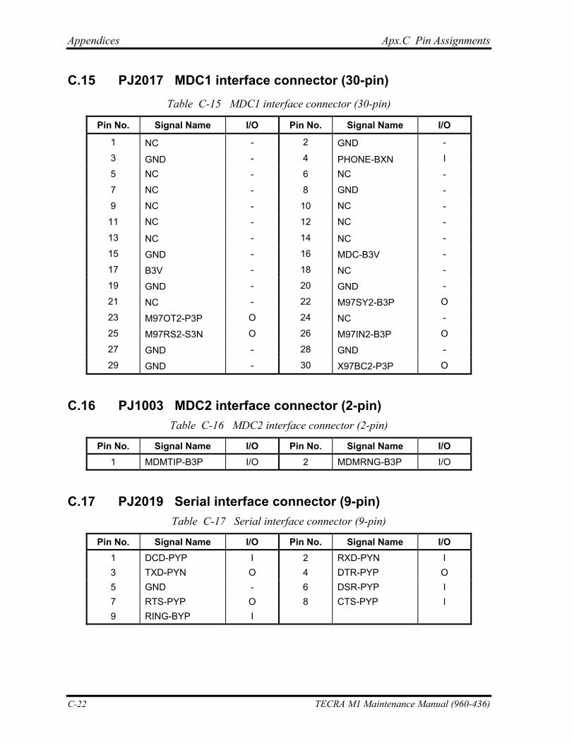
Appendices Apx.C Pin Assignments
C.15 PJ2017 MDC1 interface connector (30-pin) Table C-15 MDC1 interface connector (30-pin)
Pin No. Signal Name I/O Pin No. Signal Name I/O
1 NC - 2 GND - 3 GND - 4 PHONE-BXN I 5 NC - 6 NC - 7 NC - 8 GND - 9 NC - 10 NC -
11 NC - 12 NC - 13 NC - 14 NC - 15 GND - 16 MDC-B3V - 17 B3V - 18 NC - 19 GND - 20 GND - 21 NC - 22 M97SY2-B3P O 23 M97OT2-P3P O 24 NC - 25 M97RS2-S3N O 26 M97IN2-B3P O 27 GND - 28 GND - 29 GND - 30 X97BC2-P3P O
C.16 PJ1003 MDC2 interface connector (2-pin) Table C-16 MDC2 interface connector (2-pin)
Pin No. Signal Name I/O Pin No. Signal Name I/O 1 MDMTIP-B3P I/O 2 MDMRNG-B3P I/O
C.17 PJ2019 Serial interface connector (9-pin) Table C-17 Serial interface connector (9-pin)
Pin No. Signal Name I/O Pin No. Signal Name I/O 1 DCD-PYP I 2 RXD-PYN I 3 TXD-PYN O 4 DTR-PYP O 5 GND - 6 DSR-PYP I 7 RTS-PYP O 8 CTS-PYP I 9 RING-BYP I
C-22 TECRA M1 Maintenance Manual (960-436)
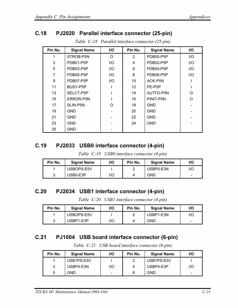
Appendix C Pin Assignments Appendices
C.18 PJ2020 Parallel interface connector (25-pin) Table C-18 Parallel interface connector (25-pin)
Pin No. Signal Name I/O Pin No. Signal Name I/O 1 STROB-P5N O 2 PDB00-P5P I/O 3 PDB01-P5P I/O 4 PDB02-P5P I/O 5 PDB03-P5P I/O 6 PDB04-P5P I/O 7 PDB05-P5P I/O 8 PDB06-P5P I/O 9 PDB07-P5P I/O 10 ACK-P5N I
11 BUSY-P5P I 12 PE-P5P I 13 SELCT-P5P I 14 AUTFD-P5N O 15 ERROR-P5N I 16 PINIT-P5N O 17 SLIN-P5N O 18 GND - 19 GND - 20 GND - 21 GND - 22 GND - 23 GND - 24 GND - 25 GND -
C.19 PJ2033 USB0 interface connector (4-pin) Table C-19 USB0 interface connector (4-pin)
Pin No. Signal Name I/O Pin No. Signal Name I/O 1 USBOPS-E5V I 2 USBP0-E3N I/O 3 USB0-E3P I/O 4 GND -
C.20 PJ2034 USB1 interface connector (4-pin) Table C-20 USB1 interface connector (4-pin)
Pin No. Signal Name I/O Pin No. Signal Name I/O 1 USBOPS-E5V I 2 USBP1-E3N I/O 3 USBP1-E3P I/O 4 GND -
C.21 PJ1004 USB board interface connector (6-pin) Table C-21 USB board interface connector (6-pin)
Pin No. Signal Name I/O Pin No. Signal Name I/O 1 USB1PS-E5V I 2 USB1PS-E5V I 3 USBP4-E3N I/O 4 USBP4-E3P I/O 5 GND - 6 GND -
TECRA M1 Maintenance Manual (960-436) C-23
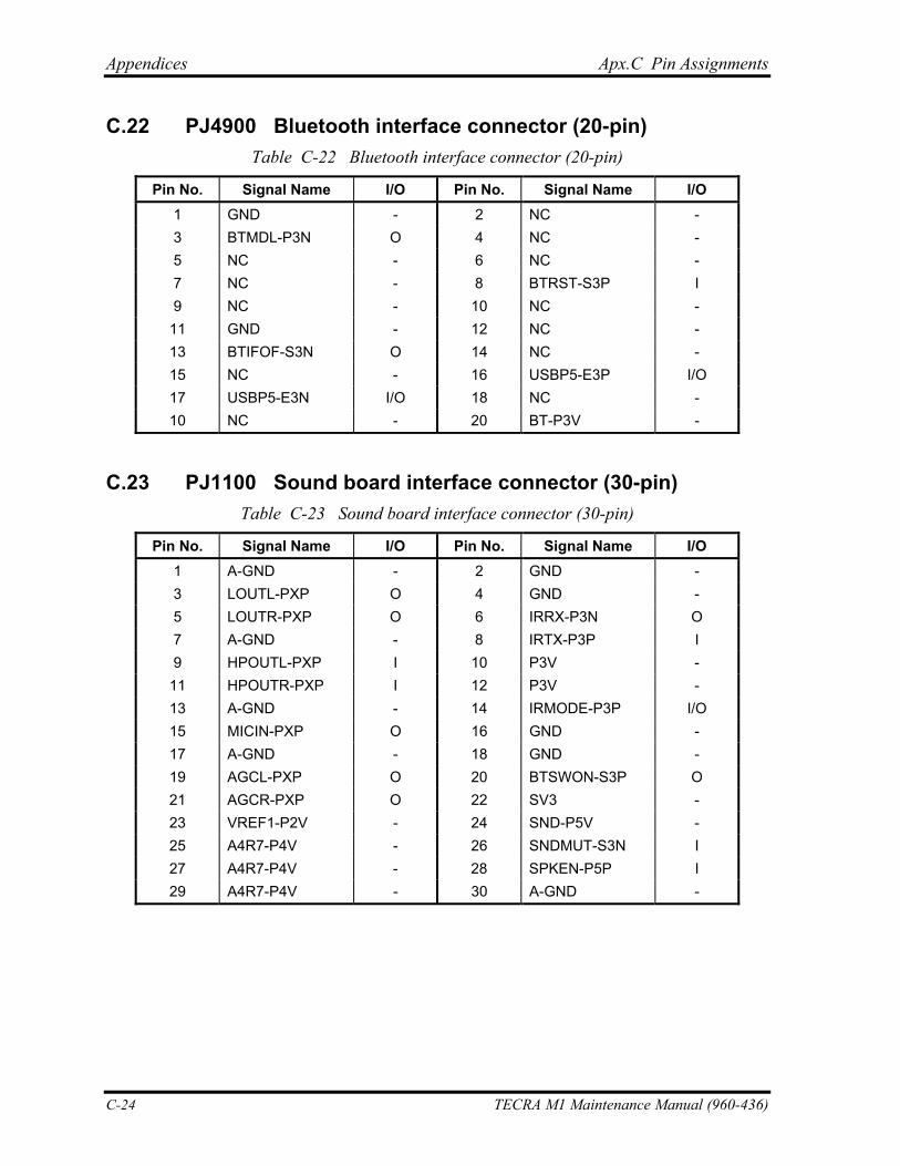
Appendices Apx.C Pin Assignments
C.22 PJ4900 Bluetooth interface connector (20-pin) Table C-22 Bluetooth interface connector (20-pin)
Pin No. Signal Name I/O Pin No. Signal Name I/O 1 GND - 2 NC - 3 BTMDL-P3N O 4 NC - 5 NC - 6 NC - 7 NC - 8 BTRST-S3P I 9 NC - 10 NC -
11 GND - 12 NC - 13 BTIFOF-S3N O 14 NC - 15 NC - 16 USBP5-E3P I/O 17 USBP5-E3N I/O 18 NC - 10 NC - 20 BT-P3V -
C.23 PJ1100 Sound board interface connector (30-pin) Table C-23 Sound board interface connector (30-pin)
Pin No. Signal Name I/O Pin No. Signal Name I/O 1 A-GND - 2 GND - 3 LOUTL-PXP O 4 GND - 5 LOUTR-PXP O 6 IRRX-P3N O 7 A-GND - 8 IRTX-P3P I 9 HPOUTL-PXP I 10 P3V -
11 HPOUTR-PXP I 12 P3V - 13 A-GND - 14 IRMODE-P3P I/O 15 MICIN-PXP O 16 GND - 17 A-GND - 18 GND - 19 AGCL-PXP O 20 BTSWON-S3P O 21 AGCR-PXP O 22 SV3 - 23 VREF1-P2V - 24 SND-P5V - 25 A4R7-P4V - 26 SNDMUT-S3N I 27 A4R7-P4V - 28 SPKEN-P5P I 29 A4R7-P4V - 30 A-GND -
C-24 TECRA M1 Maintenance Manual (960-436)
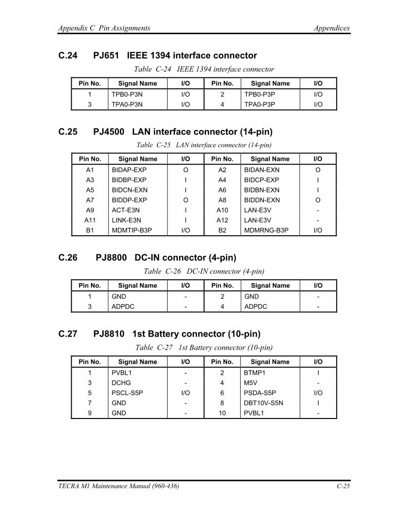
Appendix C Pin Assignments Appendices
C.24 PJ651 IEEE 1394 interface connector Table C-24 IEEE 1394 interface connector
Pin No. Signal Name I/O Pin No. Signal Name I/O 1 TPB0-P3N I/O 2 TPB0-P3P I/O 3 TPA0-P3N I/O 4 TPA0-P3P I/O
C.25 PJ4500 LAN interface connector (14-pin) Table C-25 LAN interface connector (14-pin)
Pin No. Signal Name I/O Pin No. Signal Name I/O A1 BIDAP-EXP O A2 BIDAN-EXN O A3 BIDBP-EXP I A4 BIDCP-EXP I A5 BIDCN-EXN I A6 BIDBN-EXN I A7 BIDDP-EXP O A8 BIDDN-EXN O A9 ACT-E3N I A10 LAN-E3V - A11 LINK-E3N I A12 LAN-E3V - B1 MDMTIP-B3P I/O B2 MDMRNG-B3P I/O
C.26 PJ8800 DC-IN connector (4-pin) Table C-26 DC-IN connector (4-pin)
Pin No. Signal Name I/O Pin No. Signal Name I/O 1 GND - 2 GND - 3 ADPDC - 4 ADPDC -
C.27 PJ8810 1st Battery connector (10-pin) Table C-27 1st Battery connector (10-pin)
Pin No. Signal Name I/O Pin No. Signal Name I/O 1 PVBL1 - 2 BTMP1 I 3 DCHG - 4 M5V - 5 PSCL-S5P I/O 6 PSDA-S5P I/O 7 GND - 8 DBT10V-S5N I 9 GND - 10 PVBL1 -
TECRA M1 Maintenance Manual (960-436) C-25
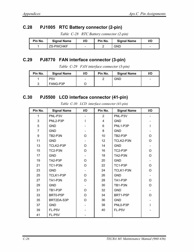
Appendices Apx.C Pin Assignments
C.28 PJ1005 RTC Battery connector (2-pin) Table C-28 RTC Battery connector (2-pin)
Pin No. Signal Name I/O Pin No. Signal Name I/O 1 ZS-PWCHKF - 2 GND -
C.29 PJ8770 FAN interface connector (3-pin) Table C-29 FAN interface connector (3-pin)
Pin No. Signal Name I/O Pin No. Signal Name I/O 1 P5V - 2 GND - 3 FANG-P3P O
C.30 PJ5500 LCD interface connector (41-pin) Table C-30 LCD interface connector (41-pin)
Pin No. Signal Name I/O Pin No. Signal Name I/O 1 PNL-P3V - 2 PNL-P3V - 3 PNL2-P3P I 4 GND - 5 GND - 6 PNL1-P3P I 7 GND - 8 GND - 9 TB2-P3N O 10 TB2-P3P O
11 GND - 12 TCLK2-P3N O 13 TCLK2-P3P O 14 GND - 15 TC2-P3N O 16 TC2-P3P O 17 GND - 18 TA2-P3N O 19 TA2-P3P O 20 GND - 21 TC1-P3N O 22 TC1-P3P O 23 GND - 24 TCLK1-P3N O 25 TCLK1-P3P O 26 GND - 27 TA1-P3N O 28 TA1-P3P O 29 GND - 30 TB1-P3N O 31 TB1-P3P O 32 GND - 33 BRT0-P5P O 34 BRT1-P5P O 35 BRT2DA-S3P O 36 GND - 37 GND - 38 PNL0-P3P I
FL-P5V - 40 FL-P5V - 41 FL-P5V - 39
C-26 TECRA M1 Maintenance Manual (960-436)
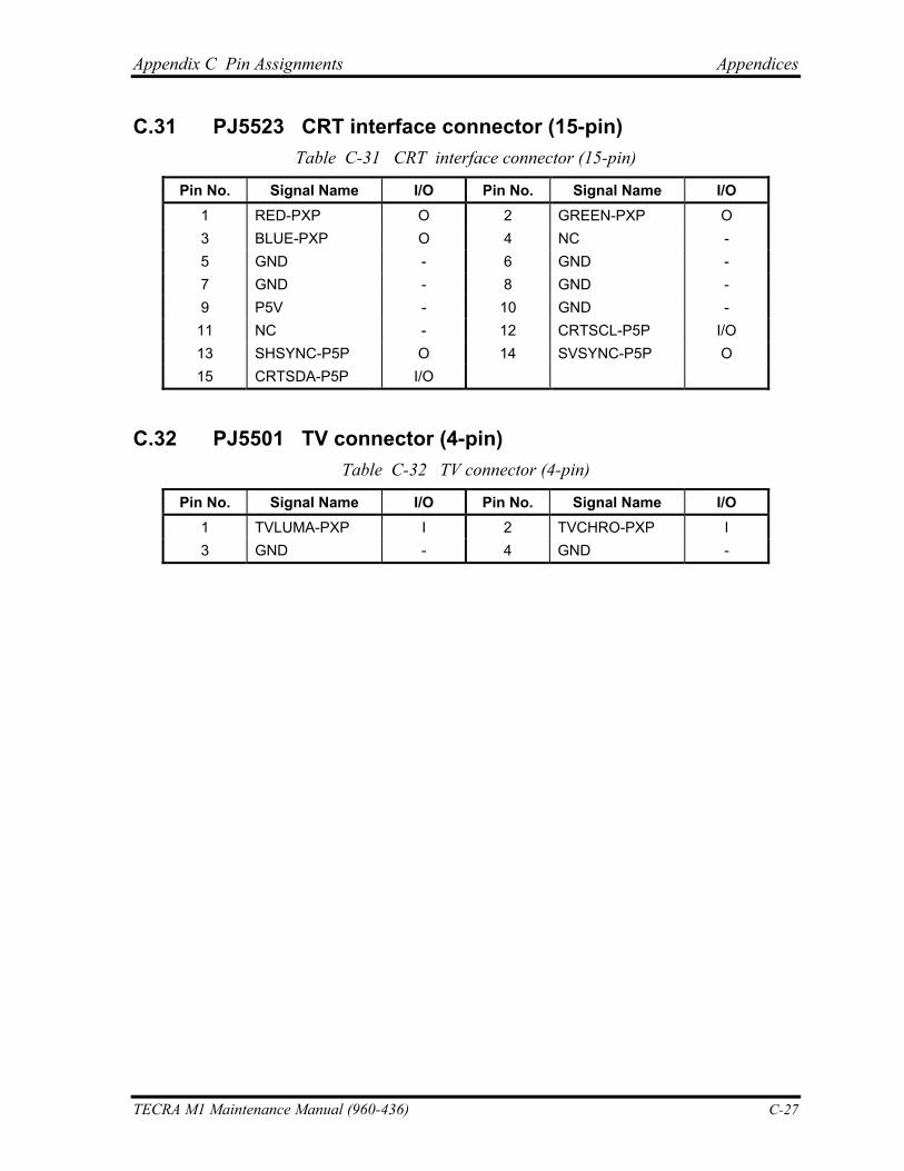
Appendix C Pin Assignments Appendices
C.31 PJ5523 CRT interface connector (15-pin) Table C-31 CRT interface connector (15-pin)
Pin No. Signal Name I/O Pin No. Signal Name I/O 1 RED-PXP O 2 GREEN-PXP O 3 BLUE-PXP O 4 NC - 5 GND - 6 GND - 7 GND - 8 GND - 9 P5V - 10 GND -
11 NC - 12 CRTSCL-P5P I/O 13 SHSYNC-P5P O 14 SVSYNC-P5P O 15 CRTSDA-P5P I/O
C.32 PJ5501 TV connector (4-pin) Table C-32 TV connector (4-pin)
Pin No. Signal Name I/O Pin No. Signal Name I/O 1 TVLUMA-PXP I 2 TVCHRO-PXP I 3 GND - 4 GND -
TECRA M1 Maintenance Manual (960-436) C-27
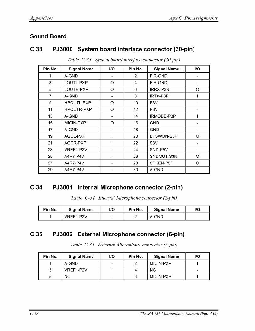
Appendices Apx.C Pin Assignments
Sound Board
C.33 PJ3000 System board interface connector (30-pin) Table C-33 System board interface connector (30-pin)
Pin No. Signal Name I/O Pin No. Signal Name I/O 1 A-GND - 2 FIR-GND - 3 LOUTL-PXP O 4 FIR-GND - 5 LOUTR-PXP O 6 IRRX-P3N O 7 A-GND - 8 IRTX-P3P I 9 HPOUTL-PXP O 10 P3V -
11 HPOUTR-PXP O 12 P3V - 13 A-GND - 14 IRMODE-P3P I 15 MICIN-PXP O 16 GND - 17 A-GND - 18 GND - 19 AGCL-PXP I 20 BTSWON-S3P O 21 AGCR-PXP I 22 S3V - 23 VREF1-P2V - 24 SND-P5V - 25 A4R7-P4V - 26 SNDMUT-S3N O 27 A4R7-P4V - 28 SPKEN-P5P O 29 A4R7-P4V - 30 A-GND -
C.34 PJ3001 Internal Microphone connector (2-pin) Table C-34 Internal Microphone connector (2-pin)
Pin No. Signal Name I/O Pin No. Signal Name I/O 1 VREF1-P2V I 2 A-GND -
C.35 PJ3002 External Microphone connector (6-pin) Table C-35 External Microphone connector (6-pin)
Pin No. Signal Name I/O Pin No. Signal Name I/O 1 A-GND - 2 MICIN-PXP I 3 VREF1-P2V I 4 NC - 5 NC - 6 MICIN-PXP I
C-28 TECRA M1 Maintenance Manual (960-436)
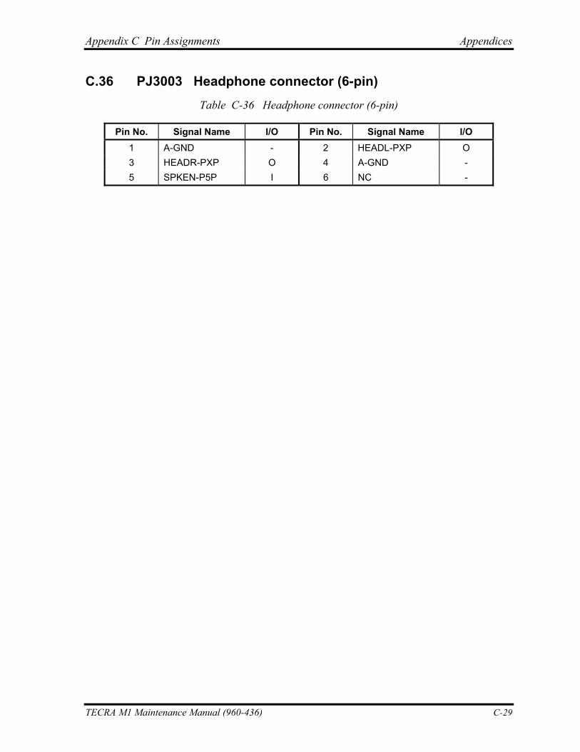
Appendix C Pin Assignments Appendices
C.36 PJ3003 Headphone connector (6-pin) Table C-36 Headphone connector (6-pin)
Pin No. Signal Name I/O Pin No. Signal Name I/O 1 A-GND - 2 HEADL-PXP O 3 HEADR-PXP O 4 A-GND - 5 SPKEN-P5P I 6 NC -
TECRA M1 Maintenance Manual (960-436) C-29
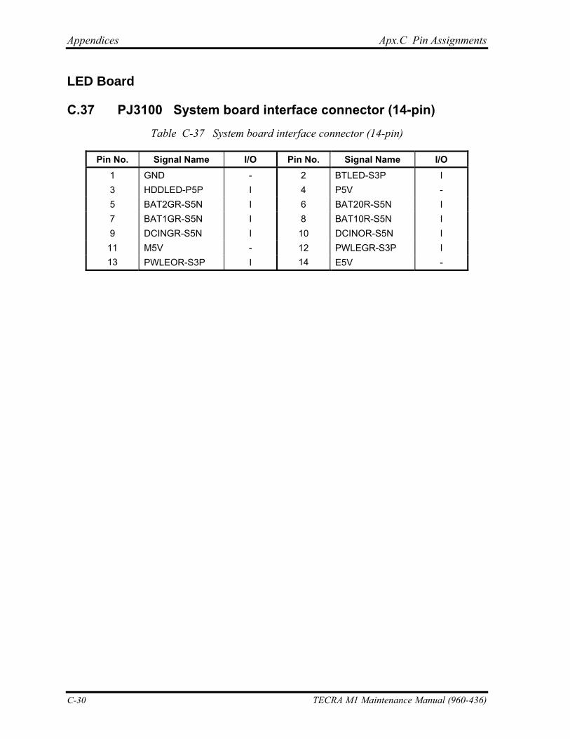
Appendices Apx.C Pin Assignments
LED Board
C.37 PJ3100 System board interface connector (14-pin) Table C-37 System board interface connector (14-pin)
Pin No. Signal Name I/O Pin No. Signal Name I/O 1 GND - 2 BTLED-S3P I 3 HDDLED-P5P I 4 P5V - 5 BAT2GR-S5N I 6 BAT20R-S5N I 7 BAT1GR-S5N I 8 BAT10R-S5N I 9 DCINGR-S5N I 10 DCINOR-S5N I
11 M5V - 12 PWLEGR-S3P I 13 PWLEOR-S3P I 14 E5V -
C-30 TECRA M1 Maintenance Manual (960-436)
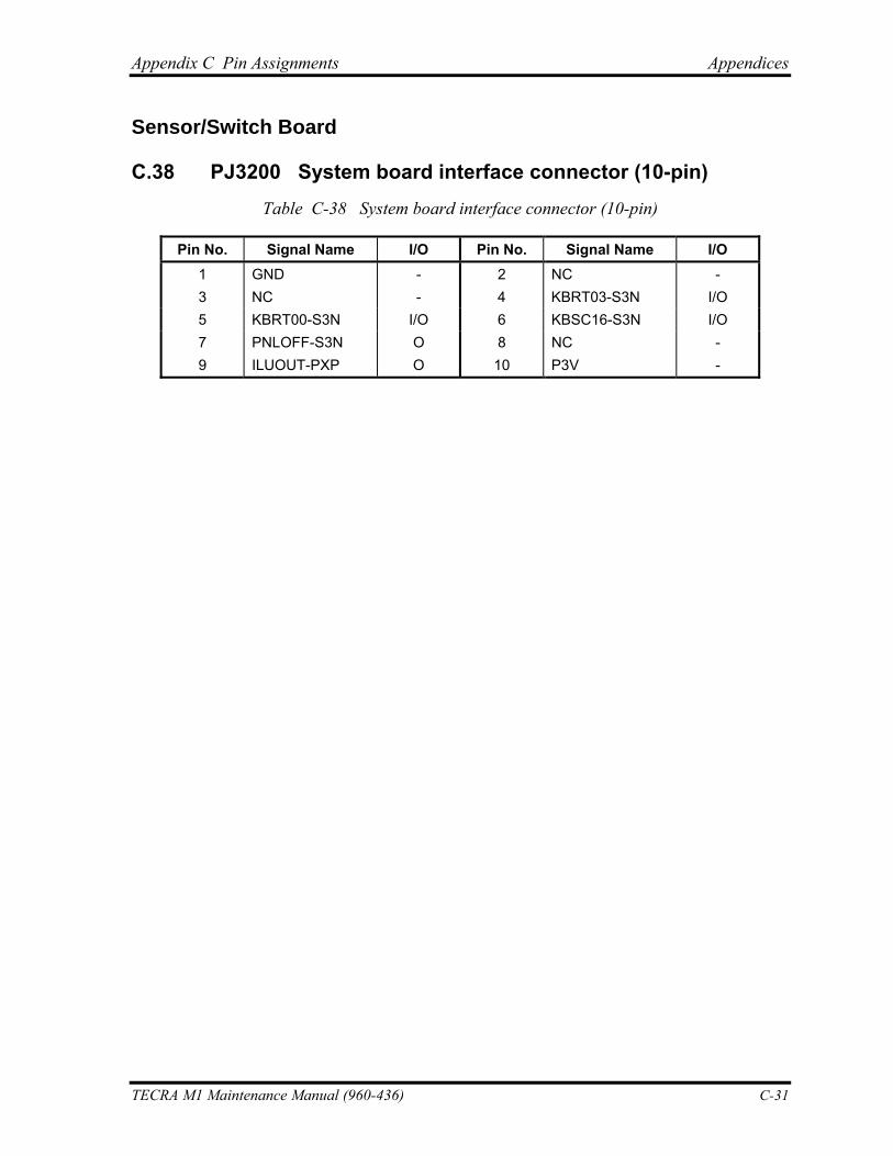
Appendix C Pin Assignments Appendices
Sensor/Switch Board
C.38 PJ3200 System board interface connector (10-pin) Table C-38 System board interface connector (10-pin)
Pin No. Signal Name I/O Pin No. Signal Name I/O 1 GND - 2 NC - 3 NC - 4 KBRT03-S3N I/O 5 KBRT00-S3N I/O 6 KBSC16-S3N I/O 7 PNLOFF-S3N O 8 NC - 9 ILUOUT-PXP O 10 P3V -
TECRA M1 Maintenance Manual (960-436) C-31
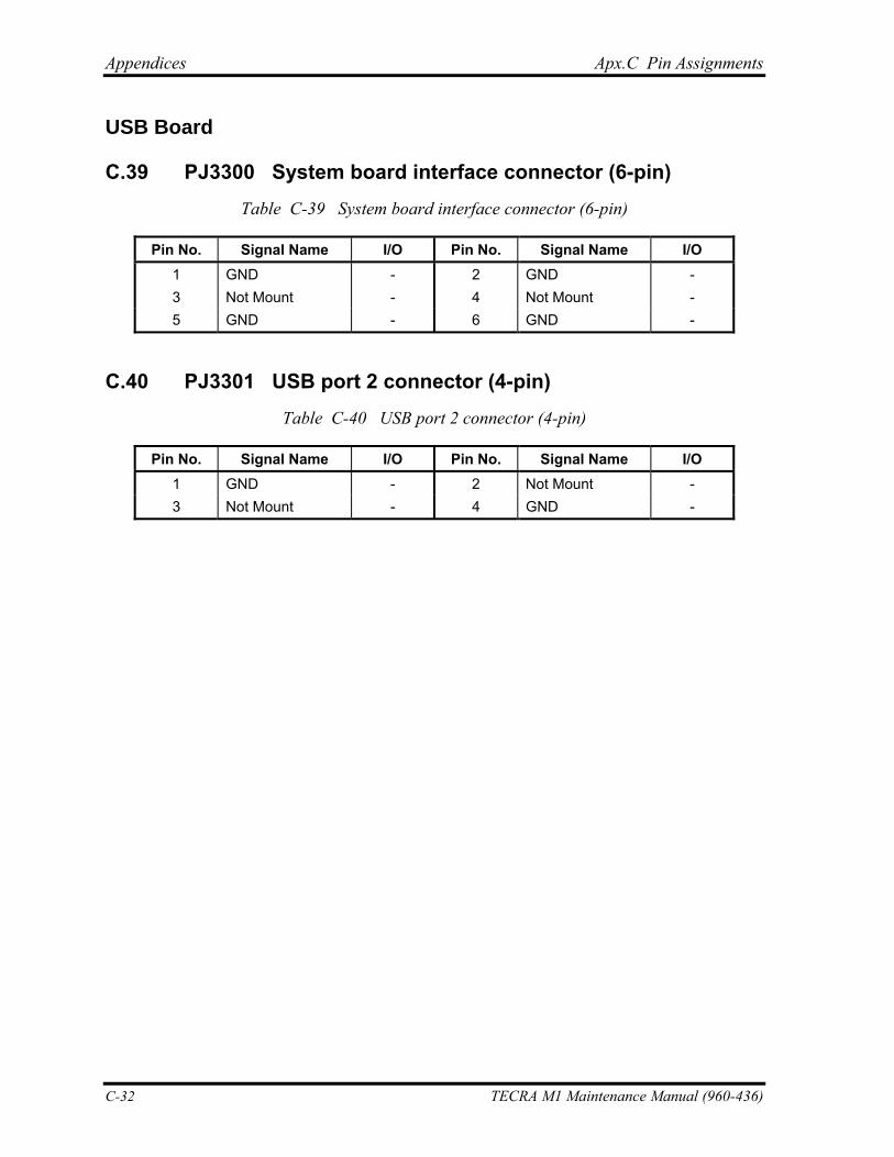
Appendices Apx.C Pin Assignments
USB Board
C.39 PJ3300 System board interface connector (6-pin) Table C-39 System board interface connector (6-pin)
Pin No. Signal Name I/O Pin No. Signal Name I/O 1 GND - 2 GND - 3 Not Mount - 4 Not Mount - 5 GND - 6 GND -
C.40 PJ3301 USB port 2 connector (4-pin) Table C-40 USB port 2 connector (4-pin)
Pin No. Signal Name I/O Pin No. Signal Name I/O 1 GND - 2 Not Mount - 3 Not Mount - 4 GND -
C-32 TECRA M1 Maintenance Manual (960-436)
Appendix C Pin Assignments Appendices
TECRA M1 Maintenance Manual (960-436) C-33
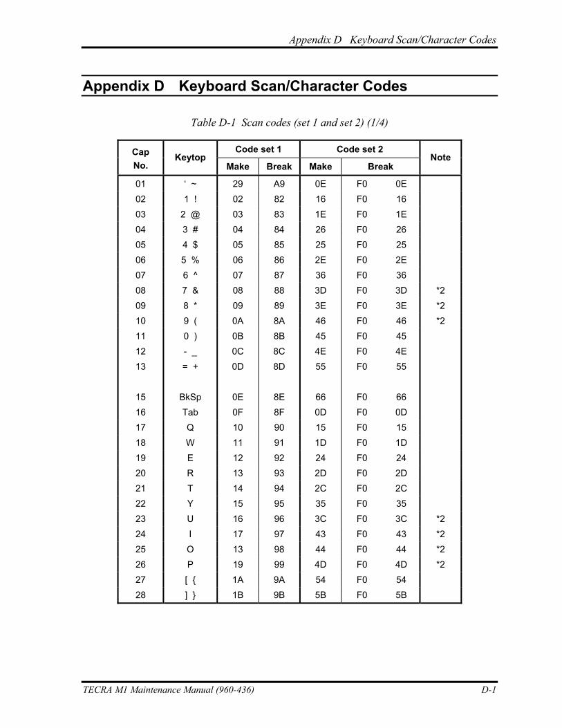
Appendix D Keyboard Scan/Character Codes
Appendix D
Appendix D Keyboard Scan/Character Codes
Table D-1 Scan codes (set 1 and set 2) (1/4)
Code set 1 Code set 2 Cap No.
Keytop Make Break Make Break
Note
01 ‘ ~ 29 A9 0E F0 0E 02 1 ! 02 82 16 F0 16 03 2 @ 03 83 1E F0 1E 04 3 # 04 84 26 F0 26 05 4 $ 05 85 25 F0 25 06 5 % 06 86 2E F0 2E 07 6 ^ 07 87 36 F0 36 08 7 & 08 88 3D F0 3D *2 09 8 * 09 89 3E F0 3E *2 10 9 ( 0A 8A 46 F0 46 *2 11 0 ) 0B 8B 45 F0 45 12 - _ 0C 8C 4E F0 4E 13 = + 0D 8D 55 F0 55
15 BkSp 0E 8E 66 F0 66 16 Tab 0F 8F 0D F0 0D 17 Q 10 90 15 F0 15 18 W 11 91 1D F0 1D 19 E 12 92 24 F0 24 20 R 13 93 2D F0 2D 21 T 14 94 2C F0 2C 22 Y 15 95 35 F0 35 23 U 16 96 3C F0 3C *2 24 I 17 97 43 F0 43 *2 25 O 13 98 44 F0 44 *2 26 P 19 99 4D F0 4D *2 27 [ 1A 9A 54 F0 54 28 ] 1B 9B 5B F0 5B
TECRA M1 Maintenance Manual (960-436) D-1
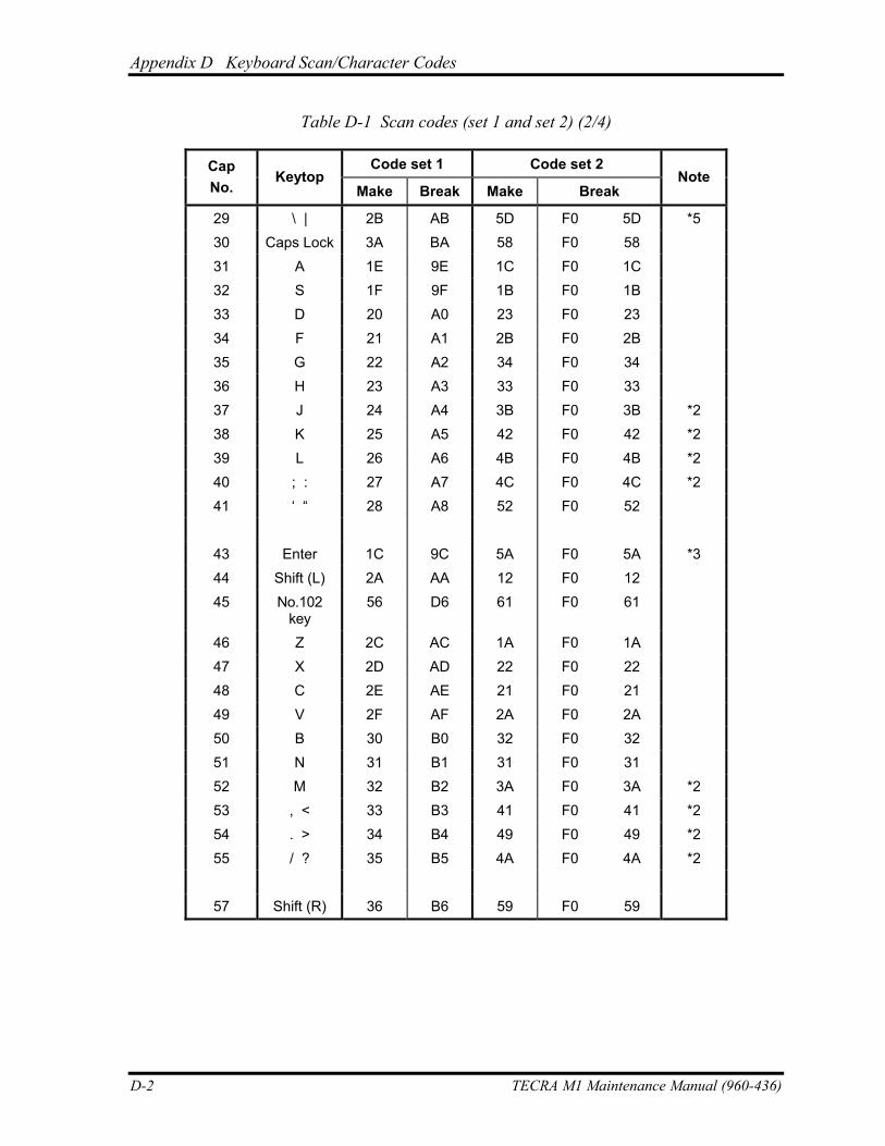
Appendix D Keyboard Scan/Character Codes
Table D-1 Scan codes (set 1 and set 2) (2/4)
Code set 1 Code set 2 Cap No.
Keytop Make Break Make Break
Note
29 \ | 2B AB 5D F0 5D *5 30 Caps Lock 3A BA 58 F0 58 31 A 1E 9E 1C F0 1C 32 S 1F 9F 1B F0 1B 33 D 20 A0 23 F0 23 34 F 21 A1 2B F0 2B 35 G 22 A2 34 F0 34 36 H 23 A3 33 F0 33 37 J 24 A4 3B F0 3B *2 38 K 25 A5 42 F0 42 *2 39 L 26 A6 4B F0 4B *2 40 ; : 27 A7 4C F0 4C *2 41 ‘ “ 28 A8 52 F0 52
43 Enter 1C 9C 5A F0 5A *3 44 Shift (L) 2A AA 12 F0 12 45 No.102
key 56 D6 61 F0 61
46 Z 2C AC 1A F0 1A 47 X 2D AD 22 F0 22 48 C 2E AE 21 F0 21 49 V 2F AF 2A F0 2A 50 B 30 B0 32 F0 32 51 N 31 B1 31 F0 31 52 M 32 B2 3A F0 3A *2 53 , < 33 B3 41 F0 41 *2 54 . > 34 B4 49 F0 49 *2 55 / ? 35 B5 4A F0 4A *2
57 Shift (R) 36 B6 59 F0 59
D-2 TECRA M1 Maintenance Manual (960-436)
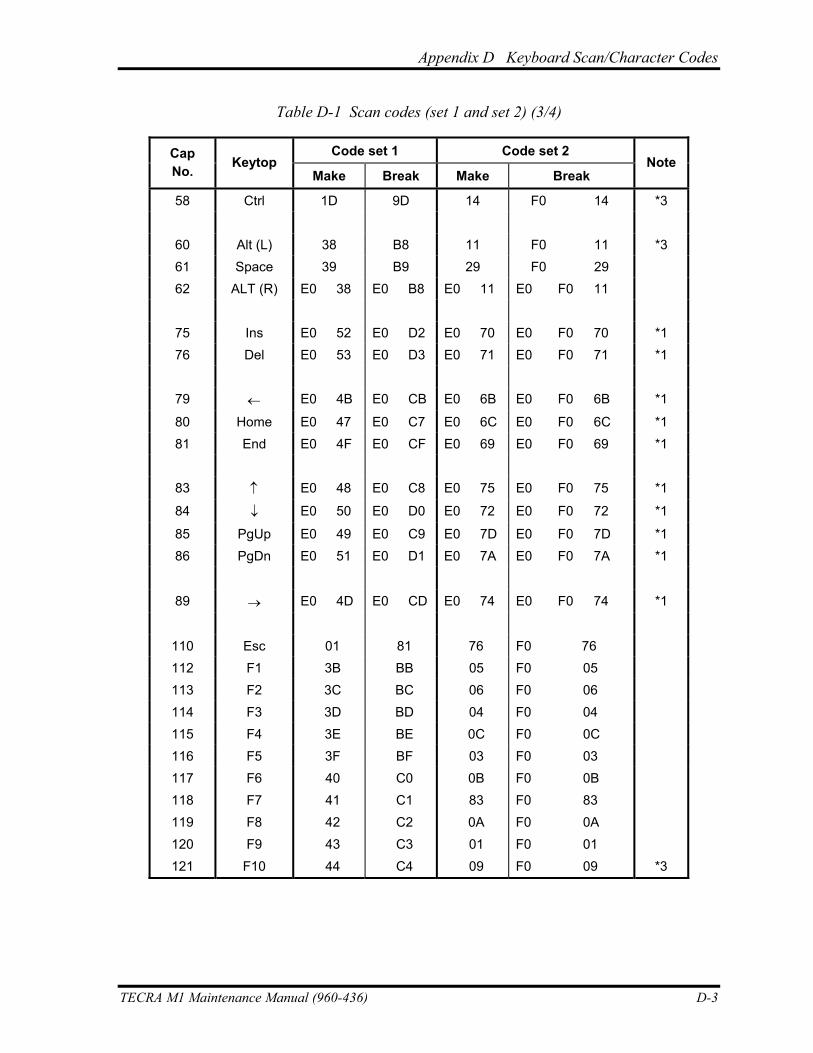
Appendix D Keyboard Scan/Character Codes
Table D-1 Scan codes (set 1 and set 2) (3/4)
Code set 1 Code set 2 Cap No. Keytop
Make Break Make Break Note
58 Ctrl 1D 9D 14 F0 14 *3
60 Alt (L) 38 B8 11 F0 11 *3 61 Space 39 B9 29 F0 29 62 ALT (R) E0 38 E0 B8 E0 11 E0 F0 11
75 Ins E0 52 E0 D2 E0 70 E0 F0 70 *1 76 Del E0 53 E0 D3 E0 71 E0 F0 71 *1
79 ← E0 4B E0 CB E0 6B E0 F0 6B *1
80 Home E0 47 E0 C7 E0 6C E0 F0 6C *1 81 End E0 4F E0 CF E0 69 E0 F0 69 *1
83 ↑ E0 48 E0 C8 E0 75 E0 F0 75 *1
84 ↓ E0 50 E0 D0 E0 72 E0 F0 72 *1
85 PgUp E0 49 E0 C9 E0 7D E0 F0 7D *1 86 PgDn E0 51 E0 D1 E0 7A E0 F0 7A *1
89 → E0 4D E0 CD E0 74 E0 F0 74 *1
110 Esc 01 81 76 F0 76 112 F1 3B BB 05 F0 05 113 F2 3C BC 06 F0 06 114 F3 3D BD 04 F0 04 115 F4 3E BE 0C F0 0C 116 F5 3F BF 03 F0 03 117 F6 40 C0 0B F0 0B 118 F7 41 C1 83 F0 83 119 F8 42 C2 0A F0 0A 120 F9 43 C3 01 F0 01 121 F10 44 C4 09 F0 09 *3
TECRA M1 Maintenance Manual (960-436) D-3
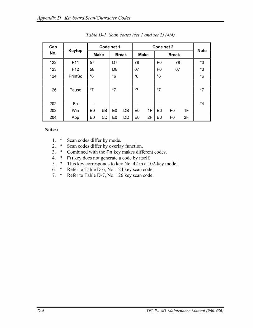
Appendix D Keyboard Scan/Character Codes
Table D-1 Scan codes (set 1 and set 2) (4/4)
Code set 1 Code set 2 Cap No. Keytop
Make Break Make Break Note
122 F11 57 D7 78 F0 78 *3 123 F12 58 D8 07 F0 07 *3 124 PrintSc *6 *6 *6 *6 *6
126 Pause *7 *7 *7 *7 *7
202 Fn — — — — *4 203 Win E0 5B E0 DB E0 1F E0 F0 1F 204 App E0 5D E0 DD E0 2F E0 F0 2F
Notes:
1. * Scan codes differ by mode. 2. * Scan codes differ by overlay function. 3. * Combined with the Fn key makes different codes. 4. * Fn key does not generate a code by itself. 5. * This key corresponds to key No. 42 in a 102-key model. 6. * Refer to Table D-6, No. 124 key scan code. 7. * Refer to Table D-7, No. 126 key scan code.
D-4 TECRA M1 Maintenance Manual (960-436)
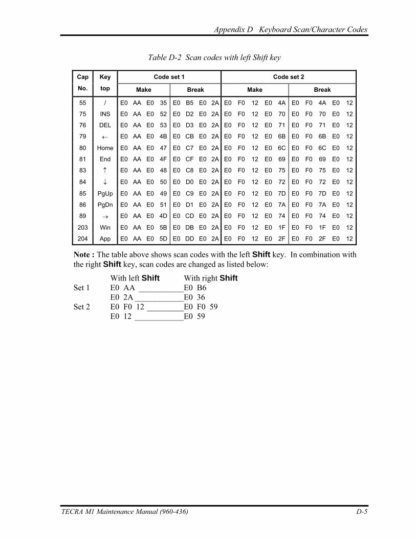
Appendix D Keyboard Scan/Character Codes
Table D-2 Scan codes with left Shift key
Code set 1 Code set 2 Cap
No.
Key
top Make Break Make Break
55 / E0 AA E0 35 E0 B5 E0 2A E0 F0 12 E0 4A E0 F0 4A E0 12
75 INS E0 AA E0 52 E0 D2 E0 2A E0 F0 12 E0 70 E0 F0 70 E0 12
76 DEL E0 AA E0 53 E0 D3 E0 2A E0 F0 12 E0 71 E0 F0 71 E0 12
79 ← E0 AA E0 4B E0 CB E0 2A E0 F0 12 E0 6B E0 F0 6B E0 12
80 Home E0 AA E0 47 E0 C7 E0 2A E0 F0 12 E0 6C E0 F0 6C E0 12
81 End E0 AA E0 4F E0 CF E0 2A E0 F0 12 E0 69 E0 F0 69 E0 12
83 ↑ E0 AA E0 48 E0 C8 E0 2A E0 F0 12 E0 75 E0 F0 75 E0 12
84 ↓ E0 AA E0 50 E0 D0 E0 2A E0 F0 12 E0 72 E0 F0 72 E0 12
85 PgUp E0 AA E0 49 E0 C9 E0 2A E0 F0 12 E0 7D E0 F0 7D E0 12
86 PgDn E0 AA E0 51 E0 D1 E0 2A E0 F0 12 E0 7A E0 F0 7A E0 12
89 → E0 AA E0 4D E0 CD E0 2A E0 F0 12 E0 74 E0 F0 74 E0 12
203 Win E0 AA E0 5B E0 DB E0 2A E0 F0 12 E0 1F E0 F0 1F E0 12
204 App E0 AA E0 5D E0 DD E0 2A E0 F0 12 E0 2F E0 F0 2F E0 12
Note : The table above shows scan codes with the left Shift key. In combination with the right Shift key, scan codes are changed as listed below:
With left Shift With right Shift Set 1 E0 AA ___________E0 B6 E0 2A ____________E0 36 Set 2 E0 F0 12 _________E0 F0 59 E0 12 ____________E0 59
TECRA M1 Maintenance Manual (960-436) D-5
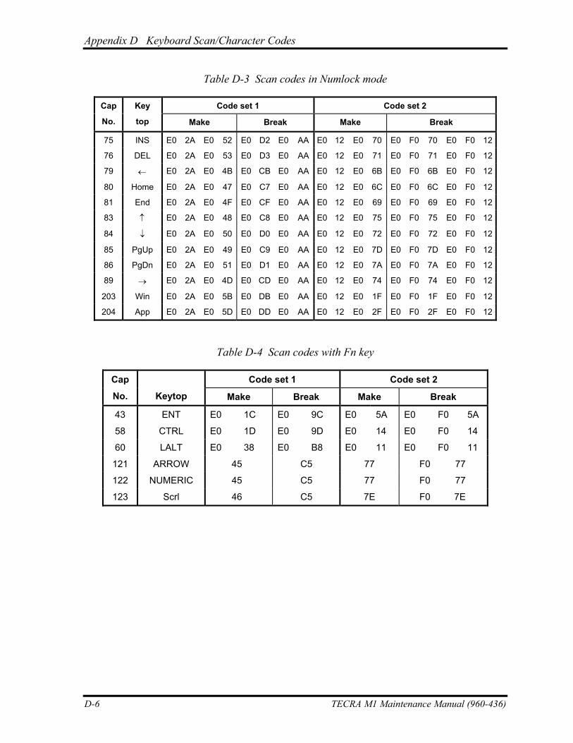
Appendix D Keyboard Scan/Character Codes
Table D-3 Scan codes in Numlock mode
Code set 1 Code set 2 Cap
No.
Key
top Make Break Make Break
75 INS E0 2A E0 52 E0 D2 E0 AA E0 12 E0 70 E0 F0 70 E0 F0 12
76 DEL E0 2A E0 53 E0 D3 E0 AA E0 12 E0 71 E0 F0 71 E0 F0 12
79 ← E0 2A E0 4B E0 CB E0 AA E0 12 E0 6B E0 F0 6B E0 F0 12
80 Home E0 2A E0 47 E0 C7 E0 AA E0 12 E0 6C E0 F0 6C E0 F0 12
81 End E0 2A E0 4F E0 CF E0 AA E0 12 E0 69 E0 F0 69 E0 F0 12
83 ↑ E0 2A E0 48 E0 C8 E0 AA E0 12 E0 75 E0 F0 75 E0 F0 12
84 ↓ E0 2A E0 50 E0 D0 E0 AA E0 12 E0 72 E0 F0 72 E0 F0 12
85 PgUp E0 2A E0 49 E0 C9 E0 AA E0 12 E0 7D E0 F0 7D E0 F0 12
86 PgDn E0 2A E0 51 E0 D1 E0 AA E0 12 E0 7A E0 F0 7A E0 F0 12
89 → E0 2A E0 4D E0 CD E0 AA E0 12 E0 74 E0 F0 74 E0 F0 12
203 Win E0 2A E0 5B E0 DB E0 AA E0 12 E0 1F E0 F0 1F E0 F0 12
204 App E0 2A E0 5D E0 DD E0 AA E0 12 E0 2F E0 F0 2F E0 F0 12
Table D-4 Scan codes with Fn key
Code set 1 Code set 2 Cap No.
Keytop Make Break Make Break
43 ENT E0 1C E0 9C E0 5A E0 F0 5A
58 CTRL E0 1D E0 9D E0 14 E0 F0 14
60 LALT E0 38 E0 B8 E0 11 E0 F0 11
121 ARROW 45 C5 77 F0 77
122 NUMERIC 45 C5 77 F0 77
123 Scrl 46 C5 7E F0 7E
D-6 TECRA M1 Maintenance Manual (960-436)
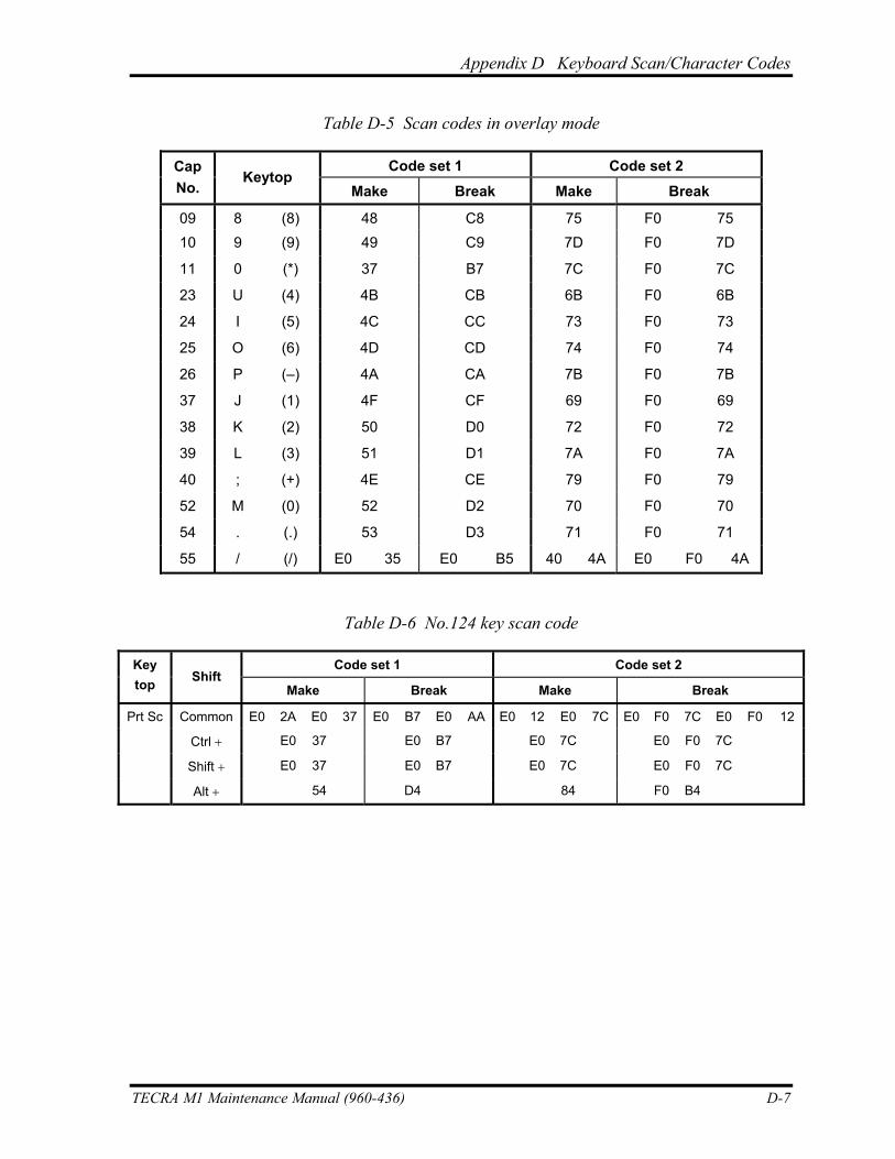
Appendix D Keyboard Scan/Character Codes
Table D-5 Scan codes in overlay mode
Code set 1 Code set 2 Cap No.
Keytop Make Break Make Break
09 8 (8) 48 C8 75 F0 75 10 9 (9) 49 C9 7D F0 7D
11 0 (*) 37 B7 7C F0 7C
23 U (4) 4B CB 6B F0 6B
24 I (5) 4C CC 73 F0 73
25 O (6) 4D CD 74 F0 74
26 P (–) 4A CA 7B F0 7B
37 J (1) 4F CF 69 F0 69
38 K (2) 50 D0 72 F0 72
39 L (3) 51 D1 7A F0 7A
40 ; (+) 4E CE 79 F0 79
52 M (0) 52 D2 70 F0 70
54 . (.) 53 D3 71 F0 71
55 / (/) E0 35 E0 B5 40 4A E0 F0 4A
Table D-6 No.124 key scan code
Code set 1 Code set 2 Key top Shift
Make Break Make Break
Prt Sc Common E0 2A E0 37 E0 B7 E0 AA E0 12 E0 7C E0 F0 7C E0 F0 12
Ctrl + E0 37 E0 B7 E0 7C E0 F0 7C
Shift + E0 37 E0 B7 E0 7C E0 F0 7C
Alt + 54 D4 84 F0 B4
TECRA M1 Maintenance Manual (960-436) D-7
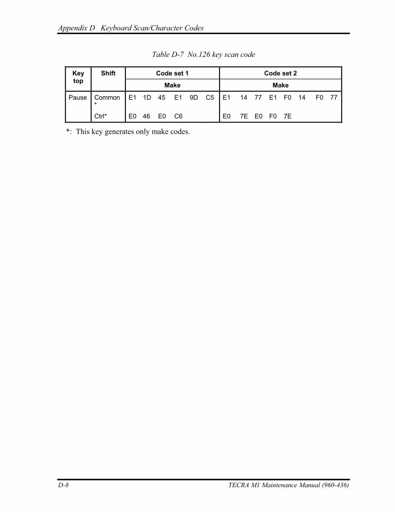
Appendix D Keyboard Scan/Character Codes
D-8 TECRA M1 Maintenance Manual (960-436)
Table D-7 No.126 key scan code
Code set 1 Code set 2 Key top
Shift
Make Make
Pause Common*
E1 1D 45 E1 9D C5 E1 14 77 E1 F0 14 F0 77
Ctrl* E0 46 E0 C6 E0 7E E0 F0 7E
*: This key generates only make codes.
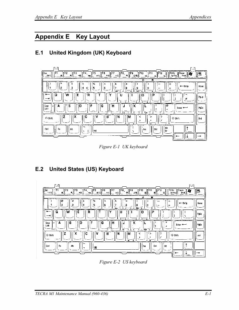
Appendix E Key Layout Appendices
Appendix E
Appendix E Key Layout
E.1 United Kingdom (UK) Keyboard
Figure E-1 UK keyboard
E.2 United States (US) Keyboard
Figure E-2 US keyboard
TECRA M1 Maintenance Manual (960-436) E-1
Appendices Appendix E Key Layout
E-2 TECRA M1 Maintenance Manual (960-436)
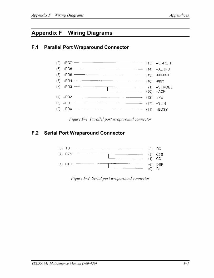
Appendix F Wiring Diagrams Appendices
Appendix F
Appendix F Wiring Diagrams
F.1 Parallel Port Wraparound Connector
-SELECT
-PINT
Figure F-1 Parallel port wraparound connector
F.2 Serial Port Wraparound Connector
Figure F-2 Serial port wraparound connector
TECRA M1 Maintenance Manual (960-436) F-1
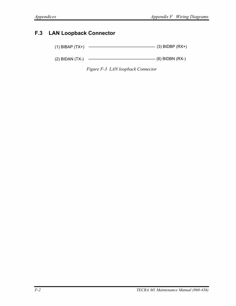
Appendices Appendix F Wiring Diagrams
F-2 TECRA M1 Maintenance Manual (960-436)
F.3 LAN Loopback Connector
(1) BIBAP (TX+)
(2) BIDAN (TX-)
(3) BIDBP (RX+)
(6) BIDBN (RX-)
Figure F-3 LAN loopback Connector
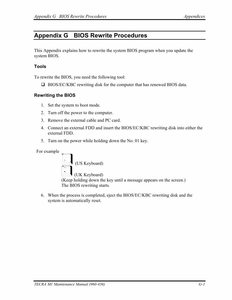
Appendix G BIOS Rewrite Procedures Appendices
Appendix G
Appendix G BIOS Rewrite Procedures
This Appendix explains how to rewrite the system BIOS program when you update the system BIOS. Tools To rewrite the BIOS, you need the following tool:
BIOS/EC/KBC rewriting disk for the computer that has renewed BIOS data. Rewriting the BIOS
1. Set the system to boot mode.
2. Turn off the power to the computer.
3. Remove the external cable and PC card.
4. Connect an external FDD and insert the BIOS/EC/KBC rewriting disk into either the external FDD.
5. Turn on the power while holding down the No. 01 key. For example
(US Keyboard)
(UK Keyboard) (Keep holding down the key until a message appears on the screen.) The BIOS rewriting starts.
6. When the process is completed, eject the BIOS/EC/KBC rewriting disk and the system is automatically reset.
TECRA M1 Maintenance Manual (960-436) G-1
Appendices Appendix G BIOS Rewrite Procedures
G-2 TECRA M1 Maintenance Manual (960-436)
Appendix H EC/KBC Rewrite Procedures Appendices
Appendix H
Appendix H EC/KBC Rewrite Procedures
This Appendix explains how to rewrite the EC/KBC system program when you update the EC/KBC system. Tools To rewrite the EC/KBC, you need the following tool:
BIOS/EC/KBC rewriting disk for the computer Rewriting the EC/KBC
NOTE: 1. Rewrite the EC/KBS only when instructed by a diagnostic disk release notice.
2. Connect the AC adaptor to the computer when you rewrite the EC/KBC.
3. Do not turn off the power while you are rewriting the EC/KBC. If the rewrite fails, it might be impossible to start up the computer.
4. If you fail to rewrite EC/KBC, then when you next turn on the power, a message may be displayed that the contents of the EC/KBC has been erased. In this case, insert the BIOS/EC/KBC rewriting disk, and the EC/KBC will be rewritten.
5. Normally it takes about 30 seconds to rewrite the EC/KBC. It may take 3 minutes (maximum), depending on the conditions of the computer or ICs. The computer is not hung up. Allow sufficient time. Never reboot or turn off the power to the computer before the rewriting is completed.
1. Set the system to boot mode. 2. Turn off the power to the computer. 3. Remove the external cable and PC Card. 4. Connect an external FDD and insert the BIOS/EC/KBC rewriting disk into either the
external or built-in FDD. 5. Turn on the power while holding down the Tab key. (Keep holding down the key
until a message appears on the screen.) The BIOS/EC/KBC rewriting starts. 6. When the EC/KBC rewrite is completed, the system is automatically turned off.
TECRA M1 Maintenance Manual (960-436) H-1
Appendices Appendix H EC/KBC Rewrite Procedures
H-2 TECRA M1 Maintenance Manual (960-436)
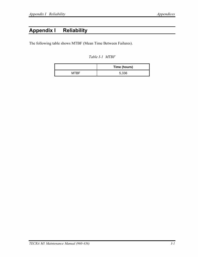
Appendix I Reliability Appendices
Appendix I
Appendix I Reliability
The following table shows MTBF (Mean Time Between Failures).
Table I-1 MTBF
Time (hours)
MTBF 5,336
TECRA M1 Maintenance Manual (960-436) I-1
Appendices Appendix I Reliability
I-2 TECRA M1 Maintenance Manual (960-436)


