Embed Size (px)
Citation preview
Thin Solid Films, 161 (1988) 289-304 PREPARATION AND CHARACTERIZATION 289
THE DEPOSITION AND FILM PROPERTIES OF REACTIVELY SPUTTERED TITANIUM NITRIDE
R. C. ELLWANGER* AND J. M. TOWNER Philips Research Laboratories Sunnyvale, Signetics Corporation, Sunnyvale, CA 94088 (U.S.A.)
(Received December 11, 1987; accepted January 11, 1988)
Titanum nitride films were prepared by reactive d.c. magnetron sputtering from a titanium target in a working gas mixture of Ar+N2. Film preparation was examined with respect to kinetics during reactive sputtering. Rutherford backscatter- ing, Auger electron spectroscopy, transmission electron microscopy and electron diffraction were used to determine film composition, impurity levels and microstruc- ture. The stoichiometric TiN films were found to possess a single-phase f.c.c. structure and demonstrated good diffusion barrier integrity in an AI/TiN/Si structure at temperatures below 550 °C. Interposition of a thin 60/~ titanium layer at the TiN-Si interface yielded low contact resistance to p+- and n+-Si regions. The limitation of reactively sputtered TiN diffusion barrier layers was determined to be their effect on the electromigration of the overlying aluminum, an effect which has not previously been reported. The insertion of a TiN layer between the aluminum and the underlying SiO2 shifted the electromigration failure mode from open- to short-circuit formation and reduced the median time to failure (MTF) by more than an order of magnitude. The MTF of the composite AI/TiN conductor was a factor of 5 less than that for a comparable AI/TiW conductor. Preliminary experimentation with layered AI/Ti conductors revealed the electromigration failure mode also to be short-circuit formation.
1. INTRODUCTION
Numerous reports in the literature deal with the formation of refractory metal nitride and carbide films. Most of these discuss the application of such materials as wear-resistant tool 1-3, optical 4 or decorative 5 coatings. Refractory metal nitrides and carbides have also been investigated for possible applications within the microelectronics industry. In particular, thin titanium nitride layers have been reported to possess some desirable properties for integrated circuit (IC) technology 6.
Titanium nitride (TIN) has been reported to be a good diffusion barrier between silicon or silicides and aluminum 7' 8, also providing a low resistance contact in such
* Present address: Philips Research Laboratories Eindhoven, 5600 JA Eindhoven, The Netherlands.
0040-6090/88/$3.50 © Elsevier Sequoia/Printed in The Netherlands
290 R.C . ELLWANGER, J. M. TOWNER
a structure (e.g. AI/TiN/Si or A1/TiN/MeSix/Si) 9'1°. TiN films contain extremely low amounts of alkali metals and hence may be used to form nearly ideal metal- oxide-semiconductor capacitors 1~. It also has been reported that TiN does not promote aluminum whisker growth when sandwiched between two aluminum layers~2.
Titanium-tungsten (TiW) is widely used for IC fabrication as a diffusion barrier between silicides and aluminum 13. Although this material functions well in preventing the interdiffusion of the silicide and the aluminum layers, TiW is problematic in other areas. Work performed in this laboratory has shown that a TiW underlayer promotes aluminum whisker growth and consequent interlayer shorts ~4.
The purpose of this work was first to characterize the deposition process and film properties of reactively sputtered titanium nitride. A specific focus then was the comparison of TiN with the TiW films used within IC processing. The results of Towner ~4 show the presence of an underlayer to be of major importance in the electromigration behavior of aluminum. Accordingly, emphasis has been placed on determining the effect of a TiN underlayer on aluminum electromigration perfor- mance as well as its performance as a diffusion barrier and contact material.
2. EXPERIMENTAL DETAILS
Films of TiN were deposited onto 10cm diameter (111), p-type silicon substrates using a Balzers BAS 450 d.c. magnetron sputter system. This system uses a so-called "drum within a drum" design. The cathode is located on the outer cylinder facing inward, while the substrates are mounted on the rotating inner cylinder. The target-to-substrate distance was 8cm. The target material was 99.999~o pure titanium. The working gas for reactive sputtering was a mixture of argon (99.995~o) and N2 (99.99~o).
The system was evacuated to a pressure less than 2 x 10 - 7 mbar and then backfilled with argon to a pressure of 2 x 10- 3 mbar, followed by a target sputter clean of 5 min at 2 kW. Subsequently, metered flows of N2 and argon gases were introduced and allowed,to stabilize to the desired pressure for 5 min each. With both argon and N 2 now present, the d.c. plasma was then re-ignited and the target was sputtered for 5 min just prior to opening the shutter. Unless otherwise noted, all experiments were performed at a total chamber pressure of 2 x 10⁻³ mbar and a target power of 2 kW.
Prior to being loaded into the vacuum system, device substrates were precleaned in H2SO4-H202 and dilute HF solutions, rinsed and dried. Prior to deposition the substrates also received an in situ r.f. sputter etch for 5 min at 300 W which removed the equivalent of 3-4 nm of thermal SiO 2. The sputter-deposited titanium and titanium nitride layers were patterned using a BCi3-CF 4 chemistry and reactive ion etching. All other layers were patterned using conventional dry etch techniques.
Rutherford backscattering spectrometry (RBS) was used to obtain the Ti:N compositional ratio in the as-deposited films. Both channeled and glancing angle spectra were analyzed. Film depth homogeneity and impurity levels were deter-
DEPOSITON AND PROPERTIES OF REACTIVELY SPUTTERED Ti 291
mined using Auger electron spectroscopy (AES) depth profiling. The specific layer resistivity was calculated from four-point probe (electrical) and stylus profilometry (thickness) measurements.
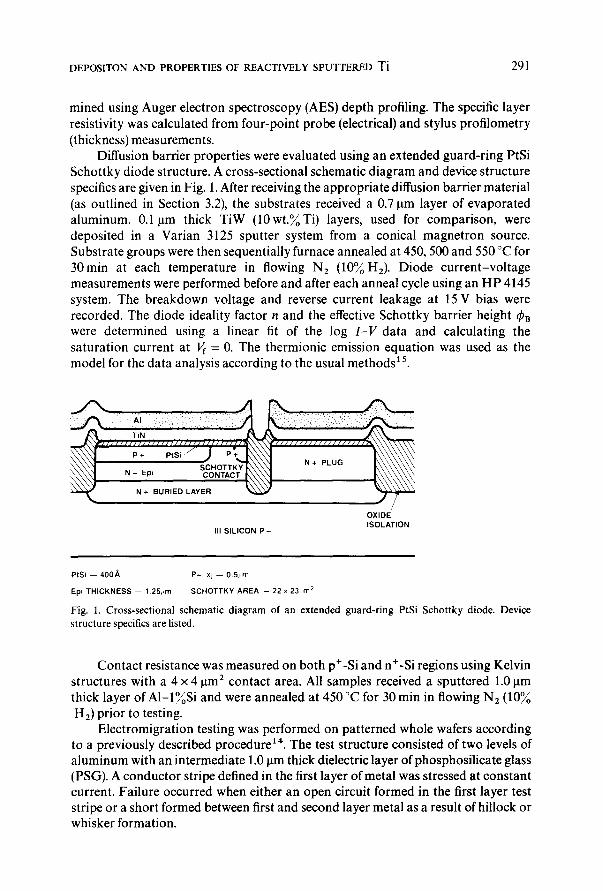
Diffusion barrier properties were evaluated using an extended guard-ring PtSi Schottky diode structure. A cross-sectional schematic diagram and device structure specifics are given in Fig. 1. After receiving the appropriate diffusion barrier material (as outlined in Section 3.2), the substrates received a 0.7 lam layer of evaporated aluminum. 0.1p.m thick TiW (10wt.~oTi) layers, used for comparison, were deposited in a Varian 3125 sputter system from a conical magnetron source. Substrate groups were then sequentially furnace annealed at 450, 500 and 550 °C for 30min at each temperature in flowing N 2 (10~oH2). Diode current-voltage measurements were performed before and after each anneal cycle using an HP 4145 system. The breakdown voltage and reverse current leakage at 15 V bias were recorded. The diode ideality factor n and the effective Schottky barrier height q~a were determined using a linear fit of the log I - V data and calculating the saturation current at Vf = 0. The thermionic emission equation was used as the model for the data analysis according to the usual methods 15.
N + B O . I E D L . Y E "
/ O X I D E I S O L A T I O N
I l l S I L I C O N P -
P tS i - - 400/~ P+ x j - - 0.5~,m
Ep i T H I C K N E S S - - 1,251,m S C H O T T K Y A R E A - - 22 x 23, m 2
Fig. 1. Cross-sectional schematic diagram of an extended guard-ring PtSi Schottky diode. Device structure specifics are listed.
Contact resistance was measured on both p+-Si and n+-Si regions using Kelvin structures with a 4 x 4 i~m 2 contact area. All samples received a sputtered 1.0 ~tm thick layer of Al-l~oSi and were annealed at 450 °C for 30 min in flowing N z (10~ H/) prior to testing.
Electromigration testing was performed on patterned whole wafers according to a previously described procedure 14. The test structure consisted of two levels of aluminum with an intermediate 1.0 pm thick dielectric layer of phosphosilicate glass (PSG). A conductor stripe defined in the first layer of metal was stressed at constant current. Failure occurred when either an open circuit formed in the first layer test stripe or a short formed between first and second layer metal as a result of hillock or whisker formation.
292 R. C. ELLWANGER, J. M. TOWNER
3. RESULTS AND DISCUSSION
3.1. Reactive sputtering kinetics When sputtering a metal in a reactive gas environment, reaction may occur at
the sputtering target, at the substrate or en route from target to substrate. The location and degree of gas-metal interaction are influenced by the type of metal and reactant gas, the system configuration and the deposition parameters. An under- standing of the location of the reaction is essential in establishing process conditions which yield specific TiN film characteristics. This section details several experiments which explored the mechanisms of nitridation for a given deposition system.
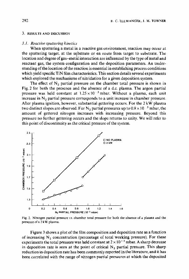
The effect of N2 partial pressure on the chamber total pressure is shown in Fig. 2 for both the presence and the absence of a d.c. plasma. The argon partial pressure was held constant at 1.25 x 10 -3 mbar. Without a plasma, each unit increase in N2 partial pressure corresponds to a unit increase in chamber pressure. After plasma ignition, however, substantial gettering occurs. For the 2 kW plasma two distinct slopes are observed. For N2 partial pressures up to 0.9 x 10- 3 mbar, the amount of gettered nitrogen increases with increasing pressure. Beyond this pressure no further gettering occurs and the slope returns to unity. We will refer to this point of discontinuity as the critical pressure of the system.
2.5
[ ] NO PLASMA 2.3 2 kW
"C
"~ 2,1
~ 1.9 - -
~: 1.7
~ 1.5
1 , 3
L I i I i I i I i I i I I I t I 0 0.2 0.4 0.6 0.8 1.0 1.2 1.4 1.6
N2 PARTIAL PRESSURE (10 -3 mbar)
Fig. 2. N i t rogen par t ia l pressure vs. chamber to ta l pressure for bo th the absence o f a plasma and the
presence of a 2 kW plasma.
Figure 3 shows a plot of the film composition and deposition rate as a function of increasing N2 concentration (percentage of total working pressure). For these experiments the total pressure was held constant at 2 × 10- 3 mbar. A sharp decrease in deposition rate is seen at the point of critical N2 partial pressure. This sharp reduction in deposition rate has been commonly reported in the literature, and it has been correlated with the range of nitrogen partial pressures at which the deposited
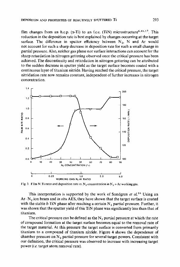
D E P O S I T O N A N D P R O P E R T I E S O F R E A C T I V E L Y S P U T T E R E D Ti 293
film changes from an h.c.p. (Qt-Ti) to an f.c.c. (TIN) microstructure 6"16'17. This reduction in the deposition rate is best explained by changes occurring at the target surface. The difference in sputter efficiency between N2, N and Ar would not account for such a sharp decrease in deposition rate for such a small change in partial pressure. Also, neither gas phase nor surface interactions can account for the sharp retardation in nitrogen gettering observed once the critical pressure has been achieved. The discontinuity and retardation in nitrogen gettering can be attributed to the sudden decrease in sputter yield as the target surface becomes coated with a continuous layer of titanium nitride. Having reached the critical pressure, the target nitridation rate now remains constant, independent of further increases in nitrogen concentration.
1,4 200
D O []
1.0 - - G
0.8
0,6
0.4
0.2
0.0 100 0 10 20 30 40 50 60 70 80 90
N2 CONCENTRATION (%)
180
z
t 160
w
z 0
140
ul a
120
i I L t I 0 0 .25 1.0 2 .3 9 .0
WORKING G A S N2/Ar RATIO
Fig. 3. Film N:Ti ratio and deposition rate vs, N 2 concentration in N 2 + A r working gas.
This interpretation is supported by the work of Sundgren e t al. 16 Using an Ar -N 2 ion beam and in s i tu AES, they have shown that the target surface is coated with the stable 8-TIN phase after reaching a certain N 2 partial pressure. Further, it was shown that the sputter yield of this TiN phase was significantly less than that of titanium.
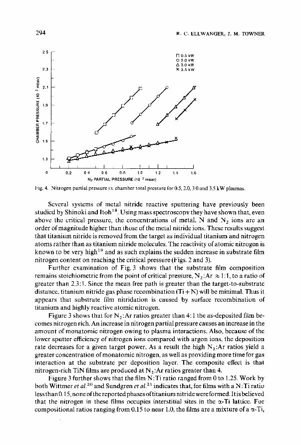
The critical pressure can be defined as the N2 partial pressure at which the rate of compound formation at the target surface becomes equal to the removal rate of the target material. At this pressure the target surface is converted from primarily titanium to a compound of titanium nitride. Figure 4 shows the dependence of chamber pressure on N 2 partial pressure for several target powers. Consistent with our definition, the critical pressure was observed to increase with increasing target power (i.e. target atom removal rate).
294 R. C. E L L W A N G E R , J. M. T O W N E R
2.5
2.3
E 2.1 'T
Q. ~ 1.7
m
~ 1.5
1,3
0
[ ] 0.5 kW O 2.0 kW
3.0 kW X 3.5 kW
/ / / / / i I = I i I t ] = I i I i L = I
0.2 0.4 0.6 0.8 1.0 1.2 1.4 1.6
N 2 PARTIAL PRESSURE (10 3 mbar)
Fig. 4. Nitrogen partial pressure vs. chamber total pressure for 0.5, 2.0, 3.0 and 3.5 kW plasmas.
Several systems of metal nitride reactive sputtering have previously been studied by Shinoki and Itoh 18. Using mass spectroscopy they have shown that, even above the critical pressure, the concentrations of metal, N and N2 ions are an order of magnitude higher than those of the metal nitride ions. These results suggest that titanium nitride is removed from the target as individual titanium and nitrogen atoms rather than as titanium nitride molecules. The reactivity of atomic nitrogen is known to be very high 19 and as such explains the sudden increase in substrate film nitrogen content on reaching the critical pressure (Figs. 2 and 3).
Further examination of Fig. 3 shows that the substrate film composition remains stoichiometric from the point of critical pressure, Nz:Ar ~ 1:1, to a ratio of greater than 2.3:1. Since the mean free path is greater than the target-to-substrate distance, titanium nitride gas phase recombination (Ti + N) will be minimal. Thus it appears that substrate film nitridation is caused by surface recombination of titanium and highly reactive atomic nitrogen.
Figure 3 shows that for Nz :Ar ratios greater than 4:1 the as-deposited film be- comes nitrogen rich. An increase in nitrogen partial pressure causes an increase in the amount of monatomic nitrogen owing to plasma interactions. Also, because of the lower sputter efficiency of nitrogen ions compared with argon ions, the deposition rate decreases for a given target power. As a result the high Nz:Ar ratios yield a greater concentration of monatomic nitrogen, as well as providing more time for gas interaction at the substrate per deposition layer. The composite effect is that nitrogen-rich TiN films are produced at N2 :Ar ratios greater than 4.
Figure 3 further shows that the film N:Ti ratio ranged from 0 to 1.25. Work by both Wittmer e t al. z ° and Sundgren e t al .2 ~ indicates that, for films with a N:Ti ratio less than 0.15, none of the reported phases of titanium nitride were formed. It is believed that the nitrogen in these films occupies interstitial sites in the ct-Ti lattice. For compositional ratios ranging from 0.15 to near 1.0, the films are a mixture o fa ct-Ti,
DEPOSITON AND PROPERTIES OF REACTIVELY SPUTTERED Ti 295
Ti2N and TiN. Combined phases of Qt-Ti and Ti2N shift to Ti2N and TiN as stoichiometry is approached. At the point of film stoichiometry only the TiN phase is seen. In agreement with the literature, electron diffraction performed from cross- sections shows films which are of stoichiometric composition to be single-phase f.c.c. TiN. Cross-sectional transmission electron microscopy (TEM) shows this film to be polycrystalline, containing grains which are vertically elongated at an average diameter of about 0.02 lam (for a film 0.1 lam in thickness).
For the range of N 2 :Ar partial pressures studied, Auger depth profiles showed the film N :Ti ratio to be homogeneous with respect to depth. The oxygen content in the film bulk ranged from below the Auger detection limit (less than 1 at.%) for substoichiometric to a high value of about 4 at.% for hyperstoichiometric films. The value for stoichiometric films was about 1-2 at.%.
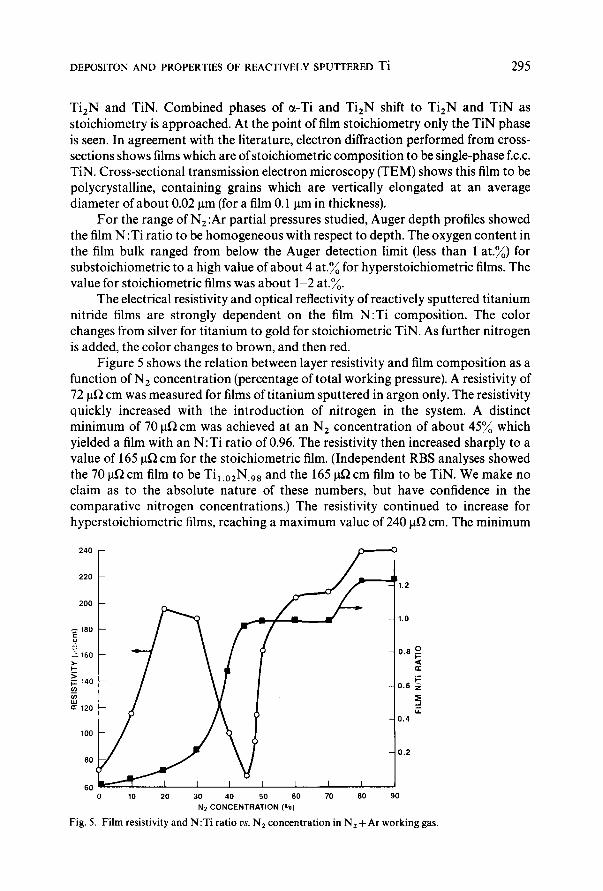
The electrical resistivity and optical reflectivity of reactively sputtered titanium nitride films are strongly dependent on the film N:Ti composition. The color changes from silver for titanium to gold for stoichiometric TiN. As further nitrogen is added, the color changes to brown, and then red.
Figure 5 shows the relation between layer resistivity and film composition as a function of N 2 concentration (percentage of total working pressure). A resistivity of 72 lad cm was measured for films of titanium sputtered in argon only. The resistivity quickly increased with the introduction of nitrogen in the system. A distinct minimum of 70 laD cm was achieved at an N 2 concentration of about 45% which yielded a film with an N:Ti ratio of 0.96. The resistivity then increased sharply to a value of 165 lad cm for the stoichiometric film. (Independent RBS analyses showed the 70 ~ cm film to be Til.o2N.9 s and the 165 lad cm film to be TiN. We make no claim as to the absolute nature of these numbers, but have confidence in the comparative nitrogen concentrations.) The resistivity continued to increase for hyperstoichiometric films, reaching a maximum value of 240 lad cm. The minimum
240
220
200
~, 180
~ 140 i:-
¢ 120 E
100
80
60 10 20 30 40 50 60 70 80 90
N2 CONCENTRATION (%)
Fig. 5. Film resistivity and N:Ti ratio v s . N 2 concentration in N 2 +Ar working gas.
296 R . C . E L L W A N G E R , J. M. T O W N E R
value of 70 ~ cm is in good agreement with results repor ted for d.c. magne t ron reactive sput ter ing when nei ther subs t ra te heat nor bias are employed 6'22. F i lms depos i ted from an r.f.-biased ca thode (with and wi thout subs t ra te heat and bias) have been repor ted to exhibi t resistivities as low as 25 Ixf~ cm (ref. 21). This m i n i m u m value was achieved at an N : T i ra t io of 0.98. All o ther studies r epor t the m i n i m u m resistivity to occur at the po in t of film s to ichiometry , sharply rising thereafter.
3.2. D i f fu s ion barr ier a n d con t ac t res i s tance p r o p e r t i e s
G u a r d - r i n g Schot tky diodes (Fig. 1) were used to evaluate the effectiveness of T iN layers as a bar r ie r to A1/Si interdiffusion in an Al /barr ier /s i l ic ide/Si structure. These d iode s tructures a l lowed the assessment of a luminum movemen t at three dist inct junc t ion depths. A change in bar r ie r height indicates in terac t ion at the 400 /~ P tS i -S i interface. Slight increases in d iode ideal i ty and reverse current leakage indicate an increasing interfacial roughening as the in terac t ion approaches the 0.5 tam p + - n junct ion. Large decreases in b r e a k d o w n vol tage show that the react ion was extended below the 0.5 ~tm p+ junct ion , while a shor t circuit indicates pene t ra t ion to the 1.25 lam ep i - to -bur ied layer junct ion .
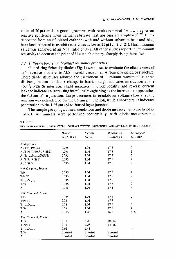
The sample groupings, anneal condi t ions and d iode measurements are listed in Table I. All anneals were per formed sequential ly, with d iode measurements
TABLE I I)IOI)E CHARACTERISTICS FOR SEVERAL CONTACT SYSTEMS (AS DEPOSITED AND AFTER SEQUENTIAL ANNEALING)
Barrier ldeality Breakdown Leakage at height (eV) factor wdtage (V) 15 V (hA)
A s deposited AI/TiN/PtSi/Si 0.795 1.04 17.5 2 A/T N/Ti(60/~)/PtSi/'Si 0.795 1.04 17.5 2 Al/Tilo2No,s/PtSi/Si 0.795 1.04 17.5 2 AI/TiW/PtSi/Si 0.795 1.04 17.5 2 AI/PtSi/Si 0.795 1.04 17.5 2
450 C anneal, 30 rain TiN 0.795 1.04 17.5 2 TiN/Ti 0.795 1.04 17.5 2 Ti~.ozNo.os 0.795 1.04 17.5 2 TiW 0.795 1.04 17.5 2 AI 0.715 1.06 17.5 6
500 C anneal, 30 min TiN 0.795 1.04 17.5 2 TiN/Ti 0.78 1.04 17.5 4 Til.o2No.g8 0.78 1.04 17.5 4 TiW 0.78 1.04 17.5 4 AI 0.715 1.06 16.5 6-50
550 C anneal, 30 min TiN 0.71 1.05 10-14 TiN/Ti 0.71 1.05 13 16 - - Ti~.o2No ~s 0.62 1.44 4 - - TiW Shorted Shorted Shorted AI Shorted Shorted Shorted - -
DEPOSITON AND PROPERTIES OF REACTIVELY SPUTTERED Ti 297
preceding and following each anneal cycle. The TiW group and an aluminum group without a barrier layer were included for reference. The other three layering groups are those titanium systems of interest.
Ting and Wittmer 1° have shown that the contact systems A1/Ti/n-Si and A1/W/Ti/n-Si yield lower specific contact resistances than either the A1/TiN/ TiSi2/n-Si or the A1/TiW/PtSi/n-Si systems. Since a thin, pure titanium layer (deposited above silicon or silicide) can be incorporated into the titanium nitride deposition sequence with relative ease, the composite TiN/Ti layer was also evaluated.
The initial diode characteristics are listed in Table I in the 'as-deposited" results. None of the five depositions had any adverse effect on diode performance. After the 450 °C anneal the aluminum has already moved to the PtSi-Si interface where no barrier layer was present; the reduction of barrier height to 0.75 eV is typical of an aluminum Schottky diode to n-Si. These data are in good agreement with those of Hosack 23 who reports a value 0.72 eV for a 450 °C anneal of the AI/PtSi/Si contact system. A slight increase in the diode ideality factor and reverse current leakage is also seen at this point in the A1/PtSi system. After the 450 °C anneal all barrier systems studied demonstrated absolute (unchanged) electrical integrity.
With the exception of the stoichiometric TiN/PtSi system a slight but significant decrease in the barrier height, accompanied by an increase in the reverse leakage current characteristics, was observed for all barrier systems after the 500 °C anneal. One explanation for this small decrease in barrier height is the presence of a small amount of either titanium or aluminum at the silicide-silicon interface. In this case a low and high barrier Schottky diode in parallel could cause this effect. However, the amount of titanium or aluminum having reached the interface would have to be extremely low, as the log I-V curve showed no distinct change in slope over the linear portion. At this temperature the AI/PtSi sample group (no barrier layer) continues to degrade.
After the 550 °C anneal substantial interdiffusion was seen for all groups. The TiW and aluminum groups are completely shorted. The titanium-rich (Til.o2N.9s) barrier film group shows a large amount of interdiffusion as witnessed by the high (1.44) ideality factor and low breakdown voltage. The barrier height of 0.62 eV is not indicative of the material which constitutes the metal-to-silicon interface. Rather, it has been artificially lowered as a result of the high leakage (non-ideality) of the junction. Although the stoichiometric titanium nitride barrier film group clearly exhibits an aluminum Schottky behavior, these films have prevented any large amounts of interdiffusion and the associated deep spiking. The diodes still exhibit near-ideal behavior; the breakdown, although lowered, is still abrupt (low leakage levels at reverse bias until avalanche breakdown).
In Table II we list those metal/silicon contact layerings studied, the dopant concentration and the relative n ÷ and p+ contact resistance for the nominal 4 I.tm × 4 p.m contacts. The titanium interfacial layer was observed to reduce contact resistance by a factor of 5 compared with that of TiSi 2, and by more than 2 orders of magnitude compared with that of Al-l~oSi contact to n ÷-Si. For contact to p÷-Si areas the TiN/Ti structure yielded values slightly higher than the AI - I~Si and
298 R. C. ELLWANGER, J. M. TOWNER
TABLE II
NORMALIZED n + AND p+ CONTACT RESISTANCES FOR VARIOUS LAYERINGS
Mater ia l Normal i zed contact resistance
n + ( ,~ 4 × 101° A s cm -3 )
A1 /T iN/T i (60 A)/Si 1.0 AI/TiNTiSi2/Si 5.5 A1/TiN/Si 190 Al/Til.o2No.g8/Si 195 AI-I%Si/Si 230
p+ (,,~ 1 x 10 l° B c m - J )
AI-I%Si/Si 1.0 AI/TiN/TiSi2/Si 1.0 AI/TiN/Ti(60 ~)/Si 2.4 A1/TiN/Si 46 Al/Til.o2No.9s/Si 48
All samples annealed at 450 °C for 30 min in N2-H 2. The 2tr range for all groups was within _+ 20% of the mean.
TiN/TiSi 2 systems. The composition of the nitride layer appears to have no influence on those p+ and n ÷ regions contacted directly by TiN. Both films display a contact resistance comparable with the Al-l%Si/n +-Si contact, and a substantially higher resistance to the p+ contact. The TiN/TiSi2/Si system also yields acceptably low values of contact resistance.
3.3. Electromigration The reliability of thin film interconnects is often limited by electromigration.
Conductor failure can result when either voids or hillocks form. Voids result in increased circuit resistance and, eventually, an open circuit in the conductor. Hillocks or whiskers cause fracture of the dielectric and, eventually, a short to a neighboring conductor. Aluminum interconnects with an underlayer of TiW are particularly prone to the formation of single-crystal aluminum whiskers 14. This is in contrast to aluminum conductors without an underlayer, where whisker growth is rarely observed.
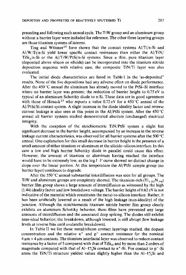
Whisker formation greatly increases the probability of short-circuit failure in multilevel metal schemes. This is graphically depicted in Fig. 6, which shows the fraction of open- or short-circuit failures in stressed AI/TiW conductors as a function of the TiW film thickness. The overlying aluminum thickness was 0.7 ~tm and the interlayer PSG thickness was 1.0 lam. The proportion of failures due to interlayer metal shorts increases exponentially with the thickness of the TiW underlayer. With 0.1 Ixm of TiW, almost all failures are due to short circuits.
Experiments performed by Grabe and Schreiber lz showed that aluminum conductors underlaid with titanium also formed enormous whiskers during current stress. When the titanium was replaced by a layer of reactively sputtered TiN, whisker growth was not observed.
To evaluate the effect of the TiN underlayer on both open-circuit and short- circuit failure, five groups of substrates were prepared. As shown in Table III, two
DEPOSITON AND PROPERTIES OF REACTIVELY SPUTTERED Ti 299
1.0 w n,"
. J
o.8
I -
{,..)
n~ 0.6
n~ 0 " l - cn 0.4
Z
~ 0.2' cO
I I I I 0 . 0 5 0.10 0.15 0 ,20
TiW THICKNESS (~.m)
w n-
. J
0.2
I . -
L )
0.4
z
0.6 o
Z 0
0.8 ~
E 1.0
0.25
Fig. 6. The effect of the underlying TiW thickness on the electromigration failure mode of 0.7 I.tm thick aluminum interconnects with a 1.0 lam PSG dielectric coating.
TABLE III M A T E R I A L S U S E D I N O P E N - S H O R T C I R C U I T E L E C T R O M I G R A T I O N S T U D Y
Conductor material AI cross-sectional area (pm 2) Failure mode
AI 3.0 30% short AI/TiW 1.9 90% short AI/Ti 1 . 0 2 N 0 . 9 8 1.8 85% short AI/TiN 2.8 90% short AI/Ti 2.5 100% short
compositions of TiN were used: stoichiometric TiN with a resistivity of 165 ~ cm and titanium-rich TiN with a resistivity of 75 ~ cm. For purposes of comparison, aluminum was also deposited directly on oxide and on a layer of sputter-deposited TiW (10wt.% Ti). In the final group, aluminum was deposited onto a layer of unreacted titanium. The underlayer thicknesses were 0.1 Ixm. All samples were metallized with 0.7 lam of aluminum in the same deposition cycle. Wafers were then annealed at 450 °C for 35 min in an N 2 + H 2 ambient.
Linewidth variations were found between sample groups. In addition, diffi- culties in wafer processing resulted in some local defects such as mousebites along the conductor stripe. To what extent these differences in linewidth affect short circuit failure is not quantitatively known. Nevertheless, Table III illustrates the effect of various underlayers on the electromigration failure mode. Whenever an underlayer was present, first-to-second layer metal shorts were the predominant failure mode, accounting for 85~o-100% of all failures. In contrast, only 30~o of the failures were due to interlayer shorts when these layers were omitted.
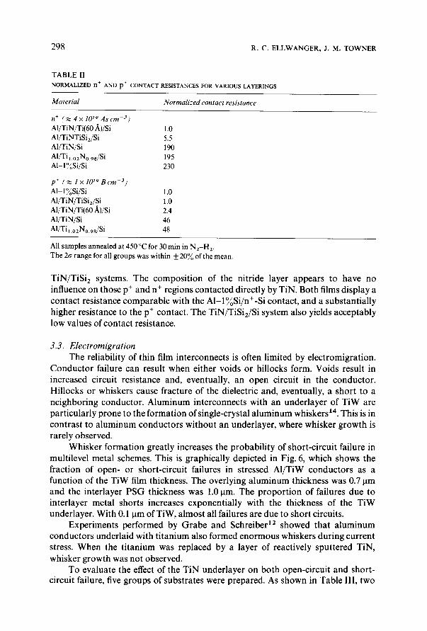
Preliminary tests with single-level, unpassivated A1/TiN test structures re- vealed a substantial reduction in the density of aluminum whiskers compared with unpassivated A1/TiW conductors. The aluminum did, however, accumulate in large, nondescript mounds (Fig. 7). Apparently, both mound formation and whisker
300 R. C. ELLWANGER~ J. M. TOWNER
(a) (b)
Fig. 7. Scanning e l e c t r o n m i c r o g r a p h s s h o w i n g (a ) a l u m i n u m w h i s k e r and (b) mound fo rmat ion in unpassivated A ] / T i N c o n d u c t o r s .
growth preferentially accelerates the short-circuit failure compared with open- circuit failure.
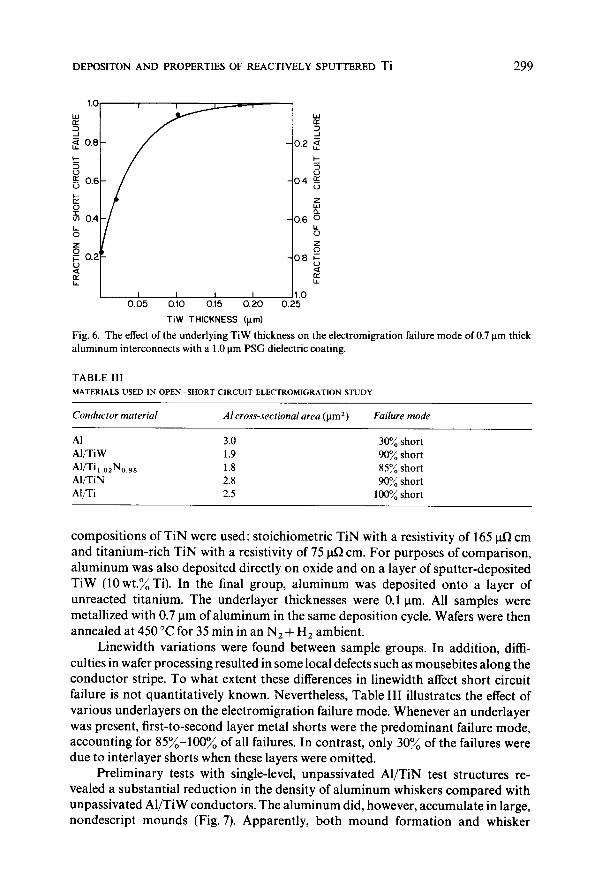
The effect of temperature on short-circuit lifetime was examined on A1/TiN conductors with the stoichiometric TiN layer. Tests were performed at temperatures ranging from 175 to 300°C and at a current density of 2.15 x 1 0 6 A cm -2. Figure 8
TEMPERATURE (°C) 300 250 200 150
I I I I
/ hi
I 0 F- 10 i tla
i-- i z <_ 1:3 LIJ
100
1 I 1 I I 1 .8 2 . 0 2 . 2 2 . 4
I O 0 0 / T ( * K - l )
Fig. 8. Arrhenius plot of short-circuit failure for AI/TiN conductors (current density, 2.15 x 10⁶ A c m - 2;
Ea = 0.46 eV).
DEPOSITON AND PROPERTIES OF REACTIVELY SPUTTERED Ti 301
shows the median time to failure (MTF) as a function of temperature. An activation energy of 0.46 eV was found. Although this value is somewhat low, it is still within the range of values expected for grain boundary diffusion in nominally pure aluminum. This result is consistent with previous work 14 which found the activation energy constant for both open-circuit and short-circuit failures.
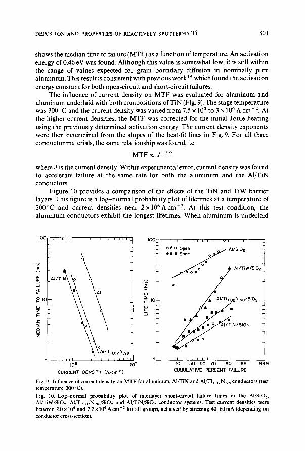
The influence of current density on MTF was evaluated for aluminum and aluminum underlaid with both compositions of TiN (Fig. 9). The stage temperature was 300°C and the current density was varied from 7.5 × 10⁵ to 3 x 10 6 A c m -2. At the higher current densities, the MTF was corrected for the initial Joule heating using the previously determined activation energy. The current density exponents were then determined from the slopes of the best-fit lines in Fig. 9. For all three conductor materials, the same relationship was found, i.e.
MTF ~ J-2.9
where J is the current density. Within experimental error, current density was found to accelerate failure at the same rate for both the aluminum and the A1/TiN conductors.
Figure 10 provides a comparison of the effects of the TiN and TiW barrier layers. This figure is a log-normal probability plot of lifetimes at a temperature of 300°C and current densities near 2 x l 0 6 A c m -z. At this test condition, the aluminum conductors exhibit the longest lifetimes. When aluminum is underlaid
100
.E
=,
o ~o
F -
Z
a I .u
I ~ I l = I i I I I I I I
~.l/Ti
I I I I I I I I I I I I I
10 6 CURRENT DENSITY (A/cm2)
~°AI/TiI.0Z N .90 I
1 0 7
I I I I I I I 1 v I I
o6 o Open , ~ j AI/Si02 e& • Short
e o / AI/TiW/Si02
/& AI/Til.ozN.98/Si02 / . . f .
I I I I I I I I I I 10 30 50 70 90 98 99.9
CUMULATIVE PERCENT FAILURE
Fig. 9. Influence of current density on MTF for aluminum, AI/TiN and Alfri 1.o2N.9s conductors (test temperature, 300 °C).
Fig. 10. Log-normal probability plot of interlayer short-circuit failure times in the AI/SiO2, AI/TiW/SiO2, Al/Tit.o2N 9s/SiO 2 and A1/TiN/SiO 2 conductor systems. Test current densities were between 2.0 x 10⁶ and 2.2 x 10⁶ A cm- 2 for all groups, achieved by stressing 40-60 mA tdepending on conductor cross-section).
302 R.C. ELLWANGER, J. M. TOWNER
with TiW, the MTF is reduced by a factor of 5. Even greater reductions in lifetime occur when either of the two TiN compositions is substituted for TiW.
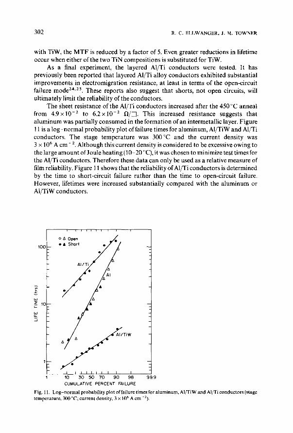
As a final experiment, the layered A1/Ti conductors were tested. It has previously been reported that layered A1/Ti alloy conductors exhibited substantial improvements in electromigration resistance, at least in terms of the open-circuit failure mode 24'25. These reports also suggest that shorts, not open circuits, will ultimately limit the reliability of the conductors.
The sheet resistance of the A1/Ti conductors increased after the 450 °C anneal from 4.9×10 -2 to 6.2×10 2 ~'~/[~. This increased resistance suggests that aluminum was partially consumed in the formation of an intermetallic layer. Figure 11 is a log-normal probability plot of failure times for aluminum, A1/TiW and A1/Ti conductors. The stage temperature was 300°C and the current density was 3 × l 0 6 A cm- 2. Although this current density is considered to be excessive owing to the large amount of Joule heating (10-20 °C), it was chosen to minimize test times for the Al/Ti conductors. Therefore these data can only be used as a relative measure of film reliability. Figure 11 shows that the reliability of A1/Ti conductors is determined by the time to short-circuit failure rather than the time to open-circuit failure. However, lifetimes were increased substantially compared with the aluminum or A1/TiW conductors.
100
v
I - -
- J
I I I I I I I I I I
o A Open • • Short
A I / /
~ AI
TiW
I I I I I I I ] I I 10 30 50 70 90 98 CUMULATIVE PERCENT FAILURE
99.9
Fig. 11. Log-normal probability plot of failure times for aluminum, AI/TiW and AI/Ti conductors (stage temperature, 300 °C; current density, 3 x 10⁶ A cm- 2).
DEPOSITON AND PROPERTIES OF REACTIVELY SPUTTERED Ti 303
4. SUMMARY AND CONCLUSIONS
The mechanism of titanium nitride film formation by reactive sputtering in an Ar + N 2 ambient have been discussed. The primary determinant is the degree and stability of target nitride coverage. This coverage is a function of target atom removal rate and system nitrogen partial pressure. For a given removal rate, a critical N 2 partial pressure can be defined, at which the target surface becomes fully covered with a TiN layer. The primary mechanism for substrate nitridation is the recombination of titanium and monatomic nitrogen, both originating from the target surface. Titanium-rich TiN films can be deposited by maintaining the N 2 partial pressure at a level below this critical pressure (for a given d.c. target power). Above this critical pressure the target surface changes from predominantly titanium to titanium nitride, and the sputter-deposited TiN films are stoichiometric. A continued increase in N2 partial pressure produces films wich are nitrogen rich, displaying a maximum N:Ti ratio of 1.25:1.
Stoichiometric TiN films were shown to possess superior diffusion barrier properties compared with sputtered TiW (10 wt.~ Ti) layers. A layered TiN/Ti(60 A) structure demonstrated the same superior diffusion barrier properties as the TiN film alone. Additionally, the TiN/Ti(60/~) structure yielded acceptably low contact resistance to n ÷- and p÷-Si regions.
The single area of poor performance observed for sputter-deposited TiN films is one which has not previously been reported, namely its effect on the electro- migration of the overlying aluminum. The electromigration failure mode shifts from open-circuit to short-circuit formation when aluminum stripes are underlaid by a TiN layer. This shift in failure mode is also accompanied by a reduction in conductor MTF of one order of magnitude. For multilevel metallization, a new generation diffusion barrier material should not promote aluminum whisker growth. An approach which appears promising is a self-aligned barrier metal. These schemes may include selective chemical vapor deposition of tungsten 26 for PtSi technologies, and nitrogen and ammonia 27.28 nitridation for TiSi2 salicide applications.
ACKNOWLEDGMENTS
Helpful discussion with Eliot Broadbent and Wilber van den Hoek is gratefully acknowledged. The authors also wish to extend their thanks to Gerard de Groot for substrate preparation, Thijs Bril and Barbara Westlund for etching of the structures, Alan Morgan for AES, Ton Kuiper for RBS, Devendra Sadana for TEM and electron diffraction, Janet DeBlasi for contact resistance structures, Hai-Au Phan Vu for TiW sputter film depositions and Doug Stadtler for sputter deposition support.
REFERENCES
1 K. Nakamura, K. Inagawa, K. TsuruokaandS. Komiya, ThinSolidFilms, 40(1977) 155. 2 R. Buhl, H. K. Pulker and E. Moll, Thin Solid Films, 80 (1981) 265. 3 A. PanandJ. Greene, ThinSolidFilms, 78(1981)25.
304 R.C. ELLWANGER, J. M. TOWNER
4 E. Valkonen, T. Karlsson, B. Karlsson and B. O. Johansson, Proc. Soc. Photo-Opt. lnstrum. Eng., 401 (1983) 41.
5 B. Zega, M. Kornmann and J. Amiguet, Thin Solid Films, 45 (1977) 577. 6 M. Wittmer, J. Vac. Sci. Teehnol. A,3(4)(1985) 1797. 7 M. Wittmer, Appl. Phys. Lett,, 37 (1980) 540. 8 H. Norstom and T. Donchev, Phys. Scr., 28 (1983) 633. 9 C.Y. Ting, J. Vac. Sci. Technol., 21 (1982) 14.
10 C.Y. Ting and M. Wittmer, Thin Solid Films, 96 (1982) 327. 11 M. Wittmer and H. Melchior, Thin Solid Films, 93 (1982) 397. 12 B.B. Grabe and H. Schreiber, SolidState Electron., 26 (1983) 1023. 13 A.N. Saxena, Proc. 1st Int. IEEE VLS1 Multilevel Interconnection Conf., 1984, IEEE, New York,
1984, p. 3. 14 J.M. Towner, Proc. 23rdlEEE Reliability Phyics Syrup., 1985, IEEE, New York, 1985, p. 81. 15 J.M. Andrews, J. Vac. Sci. Technol., 11 (1974)972. 16 J.E. Sundgren, B. O. Johansson and S. E. Karlsson, Surf Sci., 128 (1983) 265. 17 G. Lemperiere and J. M. Poitevin, Thin Solid Films, 111 (1984) 339. 18 F. Shinoki and A. Itoh, J. Appl. Phys., 46 (1975) 3381. 19 H.F. Winters, D. L. Raimondi and D. E. Horne, J. Appl. Phys., 40 (1969) 2996. 20 M. Wittmer, B. Studer and H. Melchior, J. Appl. Phys., 52 (1981) 5722. 21 J.E. Sundgren, B. O. Johansson, S. E. Karlsson and H. T. G. Hentzell, Thin Solid Films, 105 (1983)
367. 22 R.J. Shutz, Thin Solid Films, 104 (1983) 89. 23 H.H. Hosack, J. Appl. Phys., 44 (1973) 8. 24 S.S. Iyer and C. Y. Ting, Proc. 22nd IEEE Reliability Physics Syrup., 1984, IEEE, New York, 1984,
p. 273. 25 R.E. Jones, Jr., and L. D. Smith, Proc. 2nd VLSI Multilevel Interconnect Conf., 1985, IEEE, New
York, 1985, p. 194. 26 S. Swirhun, K. C. Saraswat and R. M. Swanson, IEEE Electron Device Lett., 5 (6) (1984) 209. 27 M. Delfino, E. K. Broadbent, A. E. Morgan, B. J. Burrow and M. H. Noreott, IEEE Electron Device
Lett., 6 (11) (1985) 591. 28 H. Kaneko, M. Koyanagi, S. Shimuzu, Y. Kubota and S. Kishino, Proc. Int. Electron Devices Meet.,
1985, IEEE, Washington, DC, 1985, p. 208.


