Embed Size (px)
Citation preview

ISSN:1369 7021 © Elsevier Ltd 2011SEPTEMBER 2011 | VOLUME 14 | NUMBER 9408
GaN based laser diodes (LDs) have entered widespread use as the
laser source for high-density optical data storage (e.g., Blu-ray
discs), as well as new applications in laser based projectors and
TVs. Data density for optical storage technology is limited by the
wavelength of the light source used to read and write data, with
shorter wavelengths leading to higher data density. GaN along
with InN and AlN form the only short wavelength direct bandgap
materials system that has shown both p- and n-type doping and
sufficiently long device lifetime for successful commercialization.
The need for LDs capable of faster read/write times and 3D
storage continues to drive research related to Blu-ray technology1.
Due to their high spectral purity and efficiency, lasers also make
excellent candidates for light sources in large televisions and
projectors, as well as small, portable pico-projectors (pictured in
Fig. 1). They enable over 90 % of the color gamut to be rendered
with red, green, and blue LDs; over twice the color range available
from competing technologies3.
HDTVs with screen sizes of up to 75” have been commercialized by
Mitsubishi Electric and laser projectors are commercially available from
several manufacturers. Most systems have used GaAs based red LDs
An overview of III-Nitride based laser diodes (LDs) is presented focusing on the materials challenges in each phase of device development. We discuss early breakthroughs leading to the first commercial GaN LDs, covering crystal growth, p-type doping, and defect reduction. Additional device issues, such as polarization effects, strain, and index dispersion are addressed as they apply to the development of blue and green LDs for pico-projector applications. State of the art device results are highlighted. Devices grown on non-polar and semi-polar GaN substrates address many polarization related problems present in c-plane GaN growth. Device results, advantages, and limitations of various non-polar and semi-polar systems are discussed in terms of polarization properties, Indium incorporation, extended defect formation, and critical thickness. A brief description of challenges and progress in UV LDs is also presented.
Matthew T. Hardya*, Daniel F. Feezella, Steven P. DenBaarsa,b, and Shuji Nakamuraa,b
a University of California, Materials Department, Santa Barbara, CA, 93106-5050, USAb University of California, Department of Electrical and Computer Engineering, Santa Barbara, CA, 93106-5960, USA
* Email: [email protected]
Group III-nitride lasers: a materials perspective
MT149p408_415.indd 408 11/08/2011 15:40:01

Group III-nitride lasers: a materials perspective REVIEW
SEPTEMBER 2011 | VOLUME 14 | NUMBER 9 409
and frequency doubled green and blue lasers, although arrays of high
power blue GaN LDs are entering use. Pico-projectors likely represent
the most significant new market for GaN LDs. The pico-projector
market is expected to hit $1.1 billion by 2014 and the green LD market
(both frequency doubled and semiconductor LD) is expected to reach
$500 million by 20164,5. Current pico-projectors use frequency doubled
1060 nm lasers for the green source, however due to low cost, high
efficiency, and low form factor requirements, direct emission GaN LDs
are the most likely choice for blue and green components of RGB light
sources in next generation pico-projectors. Such devices may be in
production as early as 2012.
BackgroundLDs emit light that is both highly coherent and highly directional,
allowing high fiber coupling efficiencies, coherent optics, and high
optical power densities when combined with simple optics. In general,
it is desirable to have LDs with a low threshold current density (Jth).
Device operation below Jth leads only to spontaneous emission, which
is effectively wasted. Jth can be reduced by increasing the modal
gain and reducing the cavity losses. Modal gain is the product of the
fundamental material gain (a metric controlled by the material’s
optical transition efficiency, band structure, and injection level)
and the optical confinement factor, which describes the overlap of
the optical mode with the injected carriers. Internal loss is purely
parasitic and comes from photon scattering out of the optical mode,
dopant-related free-carrier absorption, and metal contact adsorption.
Mirror loss is optical power lost out of a facet and translates directly
into useful LD output power. Mirror loss can be controlled with the
application of high-reflection (HR) or anti-reflection (AR) coatings
on the facets. HR coatings result in a decrease in Jth (due to reduced
losses) but a reduction in output power. Slope efficiency (SE) is the
slope of the optical output power versus current curve above threshold.
Typically, HR (AR) coatings can be used to decrease (increase) Jth
at the cost (benefit) of SE. SE also depends directly on injection
efficiency, which describes the portion of current above threshold
that goes to stimulated emission, and inversely on internal loss. Thus
low power LDs focus primarily on Jth reduction, while high power
device designs are focused on SE. The most commonly used power
consumption metric is wall plug efficiency (WPE), which is given by
WPE = Pout/(IopVop), where Iop and Vop are the LD operating current and
voltage. WPE is primarily dependant on SE, but achieving low Jth is also
useful. For a full treatment of LD physics, see reference 6.
Early GaN researchWhile the 1970s saw the growth of the first GaN single crystals and
observation of the first optically pumped stimulated emission7, little
progress was made on electrically injected devices until almost three
decades later. The achievement of high crystal quality GaN films
was complicated by the absence of a native substrate. The early
breakthroughs came from using AlN buffer layers grown on sapphire
substrates, and later GaN buffer layers8,9. In addition, modification of
traditional III-V metalorganic chemical vapour deposition (MOCVD)
reactor design and/or low pressure growth was required to prevent
parasitic pre-reactions between the group III metalorganic precursors
and NH3, and convective effects resulting from high GaN growth
temperatures over 1000 °C (as opposed to < 700 °C for conventional
III-Vs)10-12. In spite of drastic improvements in crystal quality,
threading dislocation (TD) densities for GaN on sapphire remained
high; between 7·108 and 1010 cm-2 13-15.
The absence of demonstrations of p-type conductivity limited
early development of III-nitride semiconductors. It wasn’t until 1989
that Amano et al. demonstrated the first p-type Mg doped GaN
using an ex situ low energy electron beam (LEEBI) treatment18. The
mechanism was later clarified by Nakamura et al., who showed H
radicals from NH3 or H2 present in the growth environment passivate
the Mg dopant. LEEBI or a simple thermal annealing in an NH3 free
environment was shown to facilitate out-diffusion of the passivating
H radicals17,18.
Fig. 1 (a)Concept for a RGB laser based projection system embedded in a mobile device. Image provided courtesy of MicroVision, Inc., www.microvision.com. (b) Far field pattern of a green LD under testing. Reprinted with permission from2. © 2010 Japan Society of Applied Physics.
(a)
(b)
MT149p408_415.indd 409 11/08/2011 15:40:03
REVIEW Group III-nitride lasers: a materials perspective
SEPTEMBER 2011 | VOLUME 14 | NUMBER 9410
In addition to crystal quality and doping issues, GaN opto-
electronic heterostructure devices must also contend with extremely
strong polarization-induced electric fields due to the lack of inversion
symmetry in the wurtzite crystal structure. These electric fields cause
a spatial separation of the electron and hole wave functions, which
leads to reductions in radiative recombination rates and radiative
efficiency19. This phenomenon is known as the quantum confined Stark
effect (QCSE). Ultimately this limits the maximum width of quantum
wells (QWs) in device active regions to prevent excessive separation
of electron and hole wave functions. Additionally, polarization-induced
electric fields cause a red shift of emission wavelength at low carrier
density due to bending of the QW band edges, and a blue shift with
increasing carrier density due to the screening of these polarization
fields19,20.
The presence of Mg doping in GaN is a major source of optical
loss, potentially as high as 65 cm-1 21. Device design must consider
the tradeoff with respect to the proximity of Mg doping to the active
region: too far away and hole injection suffers, too close and Mg based
optical loss is high21,22.
Developments in crystal growth and doping led to the first
demonstration of GaN p-n LEDs in 1991, and with further epitaxial
growth improvements, the first AlInGaN based LDs in 199623-25.
These initial LDs were grown on sapphire substrates and employed
n-/p-Al0.15Ga0.85N cladding layers, GaN waveguiding layers and a
26 period In0.2Ga0.8N/In0.05Ga0.95N MQW structure as well as an
InGaN compliance layer beneath the n-AlGaN cladding to prevent
cracking in the AlGaN. Facets were formed by reactive ion etching
due to the difficulty of cleaving GaN on sapphire25. Continued
advancements in epitaxial growth such as the implementation of short-
period strained-layer superlattices (SLSs) for the n-/p-cladding and the
implementation of standard LD technology such as ridge waveguides
and cleaved facets led to device improvements and lifetimes of up to
30 hours26-32.
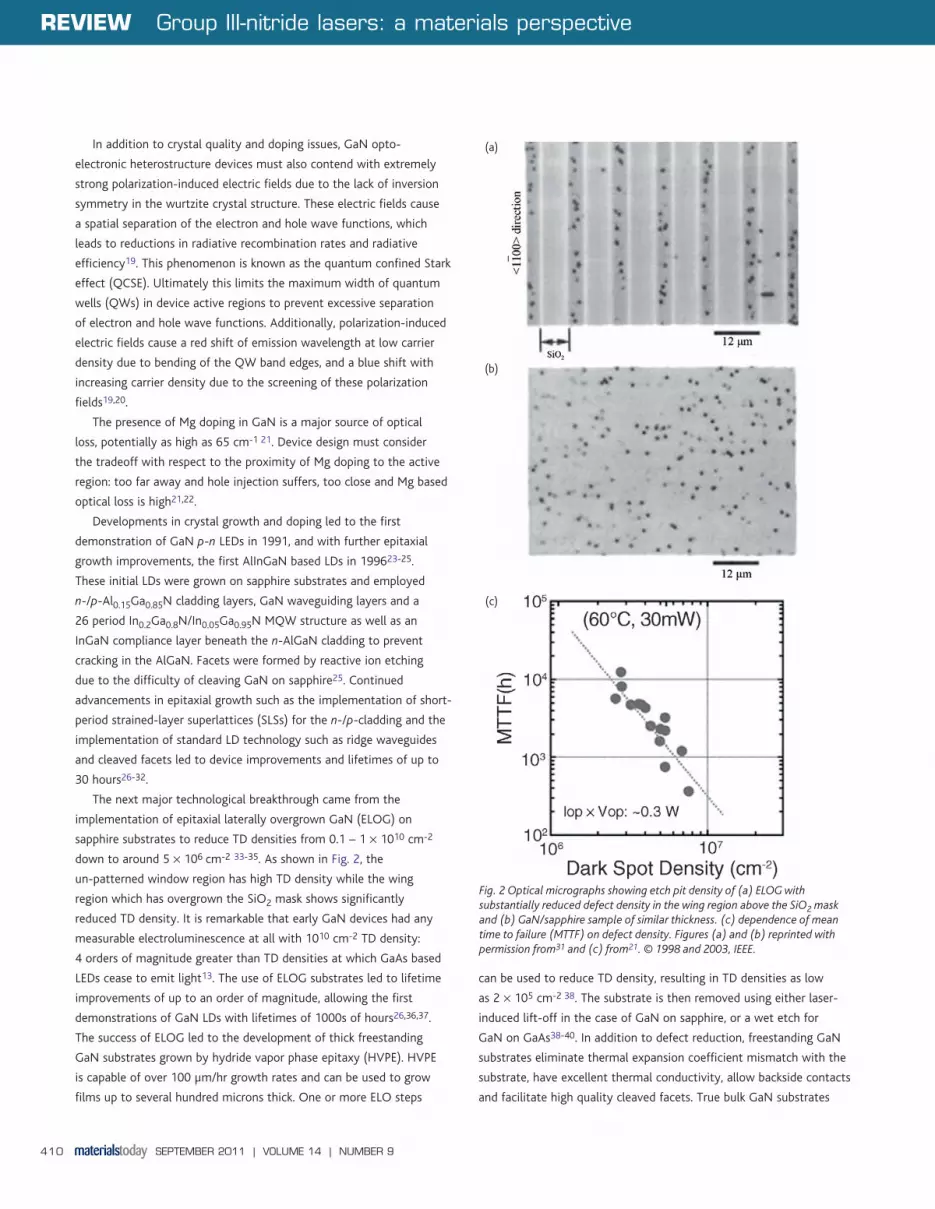
The next major technological breakthrough came from the
implementation of epitaxial laterally overgrown GaN (ELOG) on
sapphire substrates to reduce TD densities from 0.1 – 1 × 1010 cm-2
down to around 5 × 106 cm-2 33-35. As shown in Fig. 2, the
un-patterned window region has high TD density while the wing
region which has overgrown the SiO2 mask shows significantly
reduced TD density. It is remarkable that early GaN devices had any
measurable electroluminescence at all with 1010 cm-2 TD density:
4 orders of magnitude greater than TD densities at which GaAs based
LEDs cease to emit light13. The use of ELOG substrates led to lifetime
improvements of up to an order of magnitude, allowing the first
demonstrations of GaN LDs with lifetimes of 1000s of hours26,36,37.
The success of ELOG led to the development of thick freestanding
GaN substrates grown by hydride vapor phase epitaxy (HVPE). HVPE
is capable of over 100 μm/hr growth rates and can be used to grow
films up to several hundred microns thick. One or more ELO steps
can be used to reduce TD density, resulting in TD densities as low
as 2 × 105 cm-2 38. The substrate is then removed using either laser-
induced lift-off in the case of GaN on sapphire, or a wet etch for
GaN on GaAs38-40. In addition to defect reduction, freestanding GaN
substrates eliminate thermal expansion coefficient mismatch with the
substrate, have excellent thermal conductivity, allow backside contacts
and facilitate high quality cleaved facets. True bulk GaN substrates
Fig. 2 Optical micrographs showing etch pit density of (a) ELOG with substantially reduced defect density in the wing region above the SiO2 mask and (b) GaN/sapphire sample of similar thickness. (c) dependence of mean time to failure (MTTF) on defect density. Figures (a) and (b) reprinted with permission from31 and (c) from21. © 1998 and 2003, IEEE.
(a)
(b)
(c)
MT149p408_415.indd 410 11/08/2011 15:40:05

Group III-nitride lasers: a materials perspective REVIEW
SEPTEMBER 2011 | VOLUME 14 | NUMBER 9 411
with TD densities in the 101 – 104 cm-2 can be grown by high nitrogen
pressure or ammonothermal methods, however such substrates are not
yet readily available41-43.
Violet c-plane LD developmentAll currently available commercial III-nitride LDs are grown by
metalorganic chemical vapor deposition (MOCVD) on the c-plane
of the wurtzite crystal. Violet devices currently account for the
majority of revenue due to their use in high density optical data
storage. A typical device design for violet III-nitride LDs is given in
Fig. 3, and includes n- and p-AlGaN/GaN short-period SLSs (SPSLs)
for low index cladding layers and GaN or InGaN waveguiding layers
to form the separate confinement heterostructure (SCH). The MQW
active region typically has two or three QWs, although there have
been demonstrations of high performance single QW devices44. The
p-waveguiding layer is usually very lightly Mg doped or undoped to
reduce Mg related optical loss, with the p-AlGaN electron blocking
layer (EBL) placed just before or just after the p-waveguiding
layer21,28,45.
In general, there are low power consumption and high optical output
power applications, each requiring different epitaxial growth designs.
Low power consumption design typically focuses on reducing threshold
current density, primarily by increasing the confinement and reducing
optical losses. Conversely, designs for high power involve reducing
the confinement factor to spread out the optical mode and decrease
the optical power density at the facet46. Reduction of optical loss to
improve SE can be achieved by reducing the optical mode overlap with
Mg doped regions. This can be done by reducing Mg doping, moving Mg
doping farther from the active region and adjusting the waveguiding
structure to shift the optical mode towards the n-side of the device21.
Proper design of facet coatings, typically AR on the output facet and HR
coatings on the back facet can maximize SE with only minimal increase
in Jth, and high quality facet coatings can also help protect the output
facet and prevent catastrophic optical damage (COD)47.
In the past 15 years of LD research, continued crystal growth
optimization and processing improvements have resulted in state of
the art continuous wave (CW) output powers and slope efficiencies of
500 mW and 1.6 W/A, respectively, for single lateral mode devices, and
8 W and 2.1 W/A, respectively, for multi-mode devices21,46-51.
The push to c-plane blue and green LDsBlue (440 – 460 nm) semiconductor LDs are an excellent candidate
for the blue component of an RBG light source for high power, plug-in
projectors and small portable projectors known as pico-projectors. In
terms of a high power projector, LDs are attractive due to their highly
directional, high power output and long lifetimes. These qualities apply
equally well to pico-projectors, where the small form factor and high
wall plug efficiency (WPE) of LDs is also advantageous for both blue
and green (515 – 535 nm) light sources52. Laser light sources based on
second harmonic generation from InP/GaAs based LDs have recently
shown much improvement, but GaN based LDs have lower form factor
and have the potential to have higher WPEs, longer lifetimes, and lower
costs53-56.
The challenges for making longer wavelength III-nitride LDs are
numerous and become more severe with increased lasing wavelength.
To extend the emission wavelength the InN fraction in the active
region must be increased. The 10 % mismatch between the in-plane
lattice constants of GaN and InN leads to high strain in In0.18Ga0.82N
blue and In0.3Ga0.7N green QW active regions, of 1.8 % and 3.0 %,
respectively. For reference, in conventional III-V laser structures
1.5 % is considered very high strain. In addition to directly degrading
material quality, high strain also leads to increased piezoelectric
polarization in the QWs. Larger band offsets for higher In composition
QWs relative to the quantum barriers (QBs) leads to carrier transport
issues in MQW active regions, particularly for holes, which have much
lower mobility than electrons in III-nitrides. Higher In composition
layers suffer from decreased chemical stability leading to reduced
layer homogeneity and broadening of spontaneous emission line
widths in electroluminescence (EL) and photoluminescence (PL) as
well as decreased thermal stability57-59. Formation of non-radiative
recombination centers in the active region causes a drop in the
non-radiative carrier lifetime and a decrease in internal quantum
efficiency60. For example, nitrogen vacancies become increasingly
problematic with high In composition due to the elevated vapor
pressure of nitrogen in InN relative to GaN. The net effect of lower
active region quality is reduced material gain and a broadened
gain spectrum. In addition to the numerous growth challenges, the Fig. 3 Schematic of a typical epitaxial structure for a GaN based ridge waveguide LD.
MT149p408_415.indd 411 11/08/2011 15:40:07

REVIEW Group III-nitride lasers: a materials perspective
SEPTEMBER 2011 | VOLUME 14 | NUMBER 9412
dependence of the refractive index on wavelength (index dispersion)
leads to a decreasing index contrast between layers of the optical
waveguide structure, as shown by Fig. 4. For the same cladding and
waveguide structure, the confinement factor decreases with increasing
emission wavelength62,63. The summation of these effects results in
reduced modal gain for green and blue LDs and gain saturation at
lower current densities than for violet LDs64. Careful device design and
processing are required to keep optical losses to a minimum in order
to achieve lasing.
Blue c-plane LDs have been reported with a single mode output
power (slope efficiency) of 120 mW (1 W/A) and a multi-mode power
(slope efficiency) of 1.17 W (1.4 W/A)44,52,65. Green c-plane LDs with
Jth as low as 3.8 kA/cm2 and CW output powers (slope efficiency) of 50
mW (0.33 W/A) have been published64-67. Fig. 5 shows a summary of Jth
as a function of lasing wavelength. For a review of device performance
and progress of green LDs, see reference 72.
Non-polar and semi-polar growth planesEarly theoretical work predicted the absence of polarization related
electric fields for planar thin films grown on substrates orientated
orthogonally to the polar c-plane of GaN, such as the m- and a-planes,
and reduced polarization related fields on semi-polar (SP) growth
planes orientated between the polar and non-polar (NP) planes20,73.
In general, any crystal plane perpendicular to the c-plane, such as m-
and a-planes, is non-polar and any plane inclined between a non-polar
plane and c-plane is a semi-polar plane. Common NP and SP planes
are depicted schematically in Fig. 6, and Fig. 7 shows a common
calculation of the dependence of total polarization on the inclination
angle of the growth plane with respect to the c-plane. While there
is still some ambiguity in the exact polarization magnitude due to
lingering uncertainties in the piezoelectric polarization coefficients
and their variation with alloy composition, most calculations show
a cross-over in the sign of the polarization for semi-polar planes
with an inclination angle relative to c-plane between 40 – 57°74-76.
Polarization of SP InGaN with opposite sign relative to c-plane has
been experimentally confirmed at 58° (112-2) and 62° (101-1-), verifying
the zero crossing occurs at an inclination angle less than 58°77. The
early theoretical work led to a large effort to grow non-polar and
semi-polar GaN on foreign substrates. However, due to high stacking
fault densities in the 103 – 105 cm-1 range, device performance was
severely limited78,79. The stacking fault issue was finally solved by
growing freestanding c-plane GaN substrates by HVPE, and then
slicing and polishing NP and SP orientated substrates with low
dislocation and stacking fault densities40.
Unbalanced bi-axial in-plane strain in NP/SP GaN leads to a
theoretical separation of the top two valence bands. The subsequent
reduction in accessible valence band density of states should lead
to enhanced gain in NP/SP QW based LDs80,81. Early growth studies
showed severely limited In incorporation in m-plane growths
Fig. 5 Summary plot of threshold current density versus lasing wavelength50,51,59,66,68-71,91,92,96,98-100,104,105,109,111,113.
Fig. 4 Index contrast Δn of (a) AlGaN and (b) InGaN with respect to GaN for LDs operating at violet (405 nm), blue (450 nm) and green (520 nm) wavelengths. Figure based after61.
(a)
(b)
MT149p408_415.indd 412 11/08/2011 15:40:08

Group III-nitride lasers: a materials perspective REVIEW
SEPTEMBER 2011 | VOLUME 14 | NUMBER 9 413
co-loaded with c-plane, with compositions up to 2 – 3 times lower82.
Additionally, the surface morphology of m-plane homoepitaxy
exhibited large pyramidal hillocks leading to lateral thickness non-
uniformities in subsequently grown layers83. Further work showed
these pyramids formed due to spiral growth around the termination of
a partially screw-type threading dislocation with the growth surface84.
This led to the use of substrates offcut 1° towards the c-direction to
prevent hillock formation85.
The first demonstrations of violet m-plane LDs in the violet regime
closely followed the availability of free-standing GaN substrates
in 200786,87. Laser stripes oriented along the c-direction showed a
lower Jth relative to those orientated along the a-direction as a result
of anisotropic in-plane gain86,87. Studies of m-plane LEDs showed
very little QW width dependence on internal efficiency due to the
absence of QCSE, in contrast to typical c-plane devices88. This led to
the development of LDs using wide QWs in conjunction with InGaN
waveguiding layers to provide sufficient confinement of the optical mode
without the need for AlGaN cladding layers89,90. These AlGaN-cladding-
free (ACF) structures eliminate cracking issues, poor p-conductivity,
parasitic pre-reactions, and relatively high p-cladding growth
temperatures associated with p-AlGaN growth. m-plane violet LDs with
single mode output power over 500 mW and slope efficiency of 2.0 W/A
have recently been demonstrated by Kaai (now Soraa)91. These device
results are at least equivalent to state of the art c-plane LDs.
Demonstrations of blue m-plane LDs using both ACF and
traditional AlGaN clad structures followed soon after the initial
demonstrations92-96. Again Jth and output power for these initial
devices was competitive with c-plane LDs and showed drastically
reduced blue shift with increasing current density; as little as 10 nm
while c-plane devices often shifted by as much as 30 – 50 nm92,97.
Recently, Soraa demonstrated a world record CW single lateral mode
output power of 750 mW at 447 nm with 23.2 % WPE for LDs grown
on “non-c-plane” substrates98.
Continued effort was made to push m-plane out to longer lasing
wavelengths. Devices emitting in the blue-green regime with a
maximum of 500 nm were reported85,99,100. However, with increasing
wavelength, radiative efficiency, and LED output power dropped off
sharply near 500 nm. TEM investigations showed 104 – 105 cm-1 I1
type stacking faults originating from the QWs in samples emitting
around 500 nm101. These defects are likely responsible for the sudden
drop off in spontaneous emission power. I1 faults can only form due
to a growth error, and as such could be prevented by fully optimized
growth conditions, although further progress on long wavelength
m-plane LDs has not been reported.
There are a large number of low index semi-polar planes that could
potentially be used for long wavelength LDs. Early research focused
on (102-2) and (101-1), due to their relatively high In incorporation,
low piezoelectric polarization, and good LED performance, leading
to early violet LD demonstrations102-105. Stimulated emission was
observed at 514 nm on (112-2), but electrically injected green LDs
have not yet been realized106. TEM investigations discovered misfit
dislocations at each of the AlGaN cladding and InGaN waveguiding
interfaces formed due to relaxation via dislocation glide on the
c-plane107. Relaxation by TD glide is not normally seen in planar
c-plane growth because the most favorable slip system is the c-plane
Fig. 6 Schematic of various GaN crystal planes showing (a) the polar c-plane, non-polar a-plane and semipolar (112
-2) plane and (b) non-polar m-plane
and semi-polar (202-
1) and (101-
1) planes. The inclination angle ϑ with respect to the c-plane is indicated in (a).
Fig. 7 Total polarization discontinuity between (a) InxGa1-xN and GaN and (b) AlyGa1-yN and GaN as a function of inclination angle ϑ with respect to the c-plane. Figure based after74.
(a)
(b)
(a) (b)
MT149p408_415.indd 413 11/08/2011 15:40:09

REVIEW Group III-nitride lasers: a materials perspective
SEPTEMBER 2011 | VOLUME 14 | NUMBER 9414
(with a Burger’s vector b→
= 1/3 ⟨112-0⟩), which is parallel to the growth
plane and thus has no resolved shear stress. The same is true for
growth on m- and a-planes, where the growth plane is orthogonal to
the c-plane slip plane. SP planes have non-zero resolved shear stress
on the c-plane and can thus relieve stress by slip on the c-plane. For
the above mentioned (112-2) LD, high densities of misfit dislocations
less than 50 nm away from the active region likely led to high non-
radiative recombination rates, preventing lasing.
In July of 2009, Sumitomo Electric shocked the GaN LD world by
announcing lasing at 531 nm on a novel semi-polar (202-1) plane59. At
that point, the longest reported lasing wavelength was 515 nm on a
c-plane68 device. Sumitomo used quaternary AlInGaN cladding layers
latticed matched to GaN with GaN waveguiding layers to provide
index contrast without exceeding the critical thickness for relaxation
by glide on the c-plane. The critical thickness of (202-1) is 2 – 3 times
the critical thickness of (112-2) due to the difference in the SP plane
orientation relative to the c-plane, providing a larger window for
coherent growth108. A trade off emerges amongst NP/SP planes, where
m-plane has the lowest In incorporation for atmospheric pressure
MOCVD but highest critical thickness, (112-2) has the highest In
incorporation but lowest critical thickness and (202-1) falls in between
making a good compromise for long wavelength LDs with coherent
waveguiding/cladding structures.
Since the initial demonstration, Sumitomo reported CW lasing
at 526 nm with output power up to 36 mW and a reasonably low
Jth of 4.3 kA/cm2 on (202-1)109. In addition, Soraa has published CW
lasing at 521 nm with 60 mW of output power, a Jth of 7.2 kA/cm2,
a slope efficiency of 0.3 W/A, and a 10 000 hour lifetime for their
“non-c-plane” LDs98.
Ultraviolet LDsWhile there has long been interest in InGaN based LDs, interest
in AlGaN based UV LDs has only arisen in the last few years. The
GaN-AlN system spans almost the entire UV spectrum and has the
potential to replace many conventional gas and solid state UV lasers,
offering advantages in terms of cost, reliability, and portability.
AlGaN LDs as a high intensity light source have applications in
chemical analysis, bio-agent detection, photolithography, and
sterilization110,111. Many unique challenges face the development of
AlGaN based LDs. AlGaN QWs do not seem to have the robustness of
InGaN in the face of high dislocation densities, requiring sophisticated
overgrowth techniques to reduce TD density112,113. The poor
surface mobility of Al tends to require high temperature growth
(1100 – 1500 °C) or low growth rates to allow the migration of Al
ad-atoms to a step edge and preserve layer-by-layer growth, however
pre-reactions involving Al containing precursors and NH3 become a
larger problem with higher growth temperature and increasing TMA
gas phase composition112.
In addition to structural quality, doping presents a severe challenge
to electrically injected devices with increased Al content. Both Si and
Mg activation energies increase almost linearly with increasing Al
composition. The problem is particularly severe for Mg doping, which
has an activation energy around 250 meV in GaN and up to 500 meV
in AlN. AlGaN/GaN SPSLs, AlGaN/GaN polarization engineered
heterojunctions and δ-doping have shown some enhancement in hole
concentrations for films with Al compositions up to the 0.4 range.
Additionally, interstitial fluorine may act as a relatively shallow donor,
but must be diffused or implanted ex situ as epitaxially doped F will be
substitutional114. Significant work will be required to achieve good hole
injection through thick, higher Al composition cladding layers.
In spite of these challenges, there has been rapid progress towards
achieving deep UV LDs. Recently, Yoshida et al. demonstrated lasing
at 342 and 336 nm with Jth of 8 and 17 kA/cm2, respectively, claiming
drastically improved device performance due to reduced extended
defect densities in the template111,113. Work on deep UV LEDs has led
to IQE values as high as 69 % for active regions emitting at 247 nm
through the optimization of growth conditions115.
ConclusionViolet and blue c-plane laser diodes are nearing maturity, with very
high output powers and long lifetimes, leading to commercialization
for Blu-ray Discs, high power projectors, and in the near future,
pico-projectors. In spite of the large number of challenges faced,
c-plane green LDs have experienced significant progress, although
current output power, lifetime, and WPE may delay commercialization.
Semi-polar and non-polar LDs have the potential to mitigate
polarization related difficulties and have shown substantial progress,
especially in the blue and green regimes where device performance
now meets or exceeds that of state of the art c-plane LDs. Interest
is rapidly expanding into UV LDs, which may provide high power
UV light sources if structural quality and doping challenges can be
overcome.
REFERENCES1. Koda, R., et al., App. Phys Lett (2010) 97, 021101.
2. Lin, Y. -D., et al., Appl Phys Express (2010) 3, 082001.
3. Lee, J. -H., et al., Proc SPIE (2002) 4657, 138.
4. Market for embedded pico-projector modules to exceed $1bn, Semiconductor Today, Accessed online 23 May 2011, <http://www.semiconductor-today.com/news_items/2009/APRIL/INSTAT_080409.htm>.
5. Green laser diode market $500m by 2016 as pico-projector market drives growth, Semiconductor Today, Accessed online 23 May 2011, <http://www.semiconductor-today.com/news_items/2010/APRIL/YOLE_140410.htm>.
6. Coldren, L. A., and Corzine, S. W., Diode Lasers and Photonic Integrated Circuits, John Wiley & Sons, (1995).
7. Dingle, R., et al., Appl Phys Lett (1971) 19, 5.
8. Akasaki, I., et al., J Cryst Growth (1989) 98, 209.
MT149p408_415.indd 414 11/08/2011 15:40:10
Group III-nitride lasers: a materials perspective REVIEW
SEPTEMBER 2011 | VOLUME 14 | NUMBER 9 415
9. Nakamura, S., J Appl Phys (1991) 30, L1705.
10. Amano, H., et al., Appl Phys Lett (1986) 48, 353.
11. Nakamura, S., et al., Appl Phys Lett (1991) 58, 2021.
12. Kung, P., et al., Appl Phys Lett (1995) 66, 2958.
13. Lester, S. D, et al., Appl Phys Lett (1995) 66, 1249.
14. Kapolnek, D., et al., Appl Phys Lett (1995) 67, 1541.
15. Heying, B., et al., Appl Phys Lett (1996) 68, 643.
16. Amano, H., et al., Jpn J Appl Phys (1989) 28, L2112.
17. Nakamura, S., et al., Jpn J Appl Phys (1992) 31, L139.
18. Nakamura, S., et al., Jpn J Appl Phys (1992) 31, 1258.
19. Chichibu, S., et al., Appl Phys Lett (1996) 69, 4188.
20. Bernardini, F., et al., Phys Rev B (1997) 56, R10024.
21. Uchida, S., et al., IEEE J Sel Top Quantum Electron (2003) 9, 1252.
22. Kuramoto, M., et al., Phys Stat Sol (a) 192, 329.
23. Akasaki, I., et al., J Lumin (1991) 48-49, 666.
24. Nakamura, S., et al., Jpn J Appl Phys (1991) 30, L1998.
25. Nakamura, S., et al., Jpn J Appl Phys (1996) 35, L74.
26. Nakamura, S., et al., Jpn J Appl Phys (1997) 36, L1568.
27. Nakamura, S., et al., Jpn J Appl Phys (1997) 36, L1059.
28. Hansen, M., et al., Phys Stat Sol (a) (1999) 176, 59.
29. Nakamura, S., et al., Jpn J Appl Phys (1996) 35, L217.
30. Nakamura, S., et al., Appl Phys Lett (1996) 69, 1477.
31. Nakamura, S., et al., IEEE J Sel Top Quantum Electron (1998) 4, 483.
32. Nakamura, S., et al., Appl Phys Lett (1997) 70, 1417.
33. Nam, O. -H., et al. Appl Phys Lett (1997) 71, 2638.
34. Usui, A., et al., Jpn J Appl Phys (1997) 36, L899.
35. Marchland, H., et al., Appl Phys Lett (1998) 73, 747.
36. Takeya, M., et al., J Cryst Growth (2000) 221, 646.
37. Miyajima, T., et al., Mater Sci Eng B (2001) 82, 248.
38. Motoki, K., Jpn J Appl Phys (1999) 38, L140.
39. Kelly, M. K., et al., Jpn J Appl Phys (1999) 38, L217.
40. Fujito, K., et al., Phys Stat Sol (a) (2008) 205, 1056.
41. Grezegory, I., and Porowski, S., Thin Solid Films (2000) 367, 281.
42. Dwilinski, R., et al., J Cryst Growth (2009) 311, 3015.
43. Kucharski, R., et al., Appl Phys Lett (2009) 95, 131119.
44. Ryu, H. Y., et al., IEEE Photonics Technol Lett (2007) 19, 1717.
45. Nakamura, S., et al., Jpn J Appl Phys (1999) 38, L226.
46. Nam, O. H., et al., Proc. SPIE (2006) 6133, 61330N.
47. Kamikawa, T., et al., Appl Phys Lett (2009) 95, 031106.
48. Ryu, H. Y., et al., IEEE Photonics Technol Lett (2006) 18, 1001.
49. Ito, S., et al., Phys Stat Sol (a) (2007) 204, 2073.
50. Miyoshi, T., et al., Proc. SPIE (2008) 6894, 689414.
51. Brüninghoff, S., et al., Phys Stat Sol (a) (2009) 206, 1149.
52. Strauss, U., et al., Proc. SPIE (2008) 6894, 689417.
53. Steegmueller, U., et al., Proc. SPIE (2009) 7198, 719807.
54. Hartke, R., et al., Appl Phys B (2007) 87, 95.
55. Mizushima, T., et al., SID Symposium Digest of Technical Papers (2009) 40, 268.
56. Nguyen, H. K., et al., IEEE Photonics Technol Lett (2006) 18, 682.
57. Queren, D., et al., J Cryst Growth (2009) 311, 2933.
58. Ho, I., and Stringfellow, G. B., Appl Phys Lett (1996) 69, 2701.
59. Enya, Y., et al., Appl Phys Express (2009) 2, 082101.
60. Langer, T., et al., Phys Stat Sol (c) (2011) DOI: 10.1002/pssc.201001051.
61. Zhang, et al. J. Appl. Phys. (2009) 105, 023104.
62. Bergmann, M. J., and Casey, H. C., J Appl Phys (1998) 84, 1196.
63. Lermer, T., et al., Phys Stat Sol (a) (2010) 207, 1328.
64. Kojima, K., et al., Opt Express (2007) 15, 7730.
65. Michiue, A., et al., Proc. SPIE (2009) 7216, 72161Z.
66. Avramescu, A., Appl Phys Express (2010) 3, 061003.
67. Lutgen, S., et al., Phys Stat Sol (a) (2010) 207, 1318.
68. Miyoshi, T., et al., Appl Phys Express (2009) 2, 062201.
69. Miyoshi, T., et al., Phys Stat Sol (a) (2010) 207, 1389.
70. Yoshizumi et al. Appl. Phys. Lett. (2009) 2, 092101.
71. Nagahama et al. Proc. SPIE (2005) 5738, 57.
72. Ohta, H., et al., J Opt Soc Am B (2010) 27, B45.
73. Bernardini, F., and Fiorentini, V., Phys Stat Sol (b) (1999) 216, 391.
74. Romanov, A. E., et al., J Appl Phys (2006) 100, 023522.
75. Strittmatter, A., et al., Phys Stat Sol (b) (2011) 248, 561.
76. Wei, Q. Y., et al. Phys Stat Sol (a) (2010) 207, 2226.
77. Shen, H., et al., Phys Stat Sol (c) (2010) 7, 2378.
78. Haskell, B., et al., J Electron Mater (2005) 34, 357.
79. Chakraborty, A., et al., Appl Phys Lett (2004) 85, 5143.
80. Park, S. -H., and Ahn, D., Appl Phys Lett (2007) 90, 013505.
81. Park, S. -H. et al., IEEE J Quantum Electron (2007) 43, 1175.
82. Yamada, H., et al., Appl Phys Express (2008) 1, 041101.
83. Hirai, A., et al., Appl Phys Lett (2007) 91, 191906.
84. Farrell, R. M., et al. Appl Phys Lett (2010) 96, 231907.
85. Lin, Y.- D., et al., Appl Phys Express (2009) 2, 082102.
86. Schmidt, M. C., et al., Jpn J Appl Phys (2007) 46, L190.
87. Okamoto, K., et al., Jpn J Appl Phys (2007) 46, L187.
88. Kim, K. -C., Appl Phys Lett (2007) 91, 181120.
89. Feezell, D. F., et al., Jpn J Appl Phys (2007) 46, L284.
90. Farrell, R. M., et al., Jpn J Appl Phys (2007) 46, L761.
91. Raring, J. W., et al., Proc. SPIE (2010) 7602, 760218.
92. Kubota, M., et al., Appl Phys Express (2008) 1, 011102.
93. Kelchner, K. M., et al., Appl Phys Express (2009) 2, 071003.
94. Okamoto, K., et al., Jpn J Appl Phys (2007) 46, L820.
95. Lin, Y. -D., et al., Appl Phys Lett (2009) 95, 081110.
96. Kelchner, K. M., et al., Appl Phys Express (2010) 3, 092103.
97. Queren, D., et al., Appl Phys Lett (2009) 94, 081119.
98. Raring, J. W., et al., Appl Phys Express (2010) 3, 112101.
99. Okamoto, K., et al., Appl Phys Express (2008) 1, 072201.
100. Okamoto, K., et al., Appl Phys Lett (2009) 94, 071105.
101. Wu, F., et al., Appl Phys Express (2010) 96, 231912.
102. Sato, H., et al., Phys Stat Sol RRL (2007) 1, 162.
103. Tyagi, A., et al., Jpn J Appl Phys (2007) 46, L444.
104. Asamizu, H., et al., Appl Phys Express (2008) 1, 091102.
105. Asamizu, H., et al., Appl Phys Express (2009) 2, 021002.
106. Tyagi, A., et al., Appl Phys Express (2008) 1, 091103.
107. Tyagi, A., et al., Appl Phys Lett (2009) 95, 251905.
108. Young, E., et al., Appl Phys Express (2010) 3, 111002.
109. Adachi, M., et al., Appl Phys Express (2010) 3, 121001.
110. Kneissl, M., et al., Appl Phys Lett (2003) 82, 2386.
111. Yoshida, H., et al., Jpn J Appl Phys (2007) 46, 5782.
112. Khan, M. A., et al., Appl Phys Lett (2005) 44, 7191.
113. Yoshida, H., et al., Nat Photonics (2008) 2, 551.
114. Janotti, A., et al., Appl Phys Lett (2009) 95, 172109.
115. Banal, R., et al., Appl Phys Lett (2011) 99, 011902.
MT149p408_415.indd 415 11/08/2011 15:40:10


