Embed Size (px)
Citation preview

TEAC FD-55AV/ GVMINI FLEXIBLE DISK DRIVEMAINTENANCE MANUAL
REV. A

TEAC FD-5SAV ~ GV
MINI =~XI3LE DISK DRl~JE
H.~INTI:N;'_~G P.Jl..NU;lL
- i -
TABLE OF CONTENTS
Title Page
SECTION 3 THEORY OF OPERATION 300
3-1 CONSTRUCTION AND FUNCTION 301
3-1-1 General Block Diagram 301
3-1-2 Mechanical Section _ 302
3-2 CIRCUIT DESCRIPTIONS 307
3-2-1 Read Write Circuit 307
3-2-1-1 Mode selector (for read write circuit) 309
3- 2 -1 - 2 Re a d c ireuit. . . . . . . . . . . . . . . . . . . . . . . . . . . . . . . . . . . . . . . . . . . . . . . . .. 311
3-2-1-3 Wri te circui t .....•........................................... 315
3-2-1-4 Low voltage sensor 317
3-2-1-5 Function and operating waveform of read write LSI terminals 318
3-2-2 Control Circui t 326
3-2-2-1 Strap circui t 328
3-2-2-2 LED and head load control circuit ......•...................... 329
3-2-2-3 Write/erase control circuit 333
3-2-2-4 Mc>tor on gate ...........................................•..... 335
3-2-2-5 Ready detector 336
3-2-2-6 Stepping motor control circuit 339
3-2-2-7 Track counter 343
3-2-2-8 Other terminals and function of control LSI 344
3-2-2-9 Interface driver 346
3-2-3 Servo Circuit 347
3-3 FUNCTION OF TEST POINTS AND VARIABLE RESISTORS 3~8
3-3-1 Function of Test Points 349
3-3-2 Function of Variable Resistors 354
- ii -
Title Page
SECTION 4 MAINTENANCE ........................•......................... 4000
4-1 GENERAL............. . . . . . . . . . . . . . . . . . . . . . . . . . . . . . . . . . . . . . . . . . . . . .. 4001
4-1-1 Periodic Maintenance 4001
4-1~2 Check and Adjustment .' 4002
4-1-3 Maintenance Jigs and Tools 4003
4-2 PRECAUTIONS............................................... . . . . . . .. 4007
4-2-1 Torque Applied to Screws and Locking Paint 4007
4-2-2 Handling of Connectors 4008
4-2-3 Head Cable Treatment 4013
4-2-4 Initial Setting of SKA-G and SKA 4015
4-2-4-1 Cable connection and setting of power supply voltage 4015
4-2-4-2 Setting of the maximum track number 4018
4-2-4-3 Setting of step rate and settling time .~ •..................... 4018
4-2-4-4 Level disk calibration 4021
4-2-4-5 Alignment disk calibration 4023
4-2-4-6 Humidi ty setting 4026
4-2 -4 - 7 Setting 0 f SKA gain 4026
4-2-4-8 Setting of FDD straps and SKA special key 4027
4-2-5 Others 4029
4-3 PREVENTIVE MAINTENANCE 4032
4-3-1 Cleaning of Magnetic Head by Cleaning Disk 4032
4-3-2 Direct Cleaning <Single sided} 4034
4-4 CHECK AND ADJUSTMENT 4036
4-4-1 Adjustment of Set Arm Position 4036
4-4-2 Check and Adjustment of Holder Position ....•.................... 4038
4-4-3 Check and Adjustment of Arm Lifter 4041
4-4-3-1 [)()uble sided 4041
4-4-3-2 Single sided 4051
4-4 -4 Check of CSS Ass' Y -.f054
4-4-5 Check of File Protect Sensor ............•....................... 4058
4-4-6 Check of Disk Rotation Speed 4061
4-4-7 Check of Erase Gate Delay 4063
4-4-8 Check of Head Touch 4066
- iii -
4-4-9
Title
Check and Adjustment of Asymmetry
Page
4072
Check and Adjustment of Track Alignment ......................... 4084
Check and Adjustment of Track 00 Sensor ........................ 4093
Check and Adjustment of Track 00 Stopper ....................... 4100
Check and Adjustment of Index Burst Timing ..................... 4105
4077
4080Check of Resolution
Check of Read Level4-4-10
4-4-11
4-4-12
4-4-13
4-4-14
4-4-15
4-5 MAINTENANCE PARTS REPLACEMENT 4110
4-5-1 Replacement of Head Carriage Ass'y ........................•..... 4110
4-5-1-1
4-5-1-2
Replacement of v-type carriage
Replacement of L-type carriage
4110
4117
4-5-2 Replacement of Stepping MQtor Ass 'y 4121
4-5-3 Replacement of DD motor Ass'y <Spindle motor}, 4124
4-5-4 Replacement of Collet Ass'y 4126
4-5-5 Replacement of Head Load Solenoid ........•...................... 4127
4-5-6 Replacement of Track 00 Sensor Ass'y 4129
4-5-7 Replacement of PCBA MFD Control #H 4130
4-5-8
4-5-9
Replacement of PCBA Front OPT #H
Replacement of Front Bezel Ass'y
4132
4133
4-5-10 Replacement of Front Lever Ass'y 4134
4-5-11 Replacement of CSS Ass'y 4135
4-5-12 Replacement of Head Pad (Single sided) .........•................ 4136
- iv -

SECTION 3
THEORY OF OPERATION
- 300 -
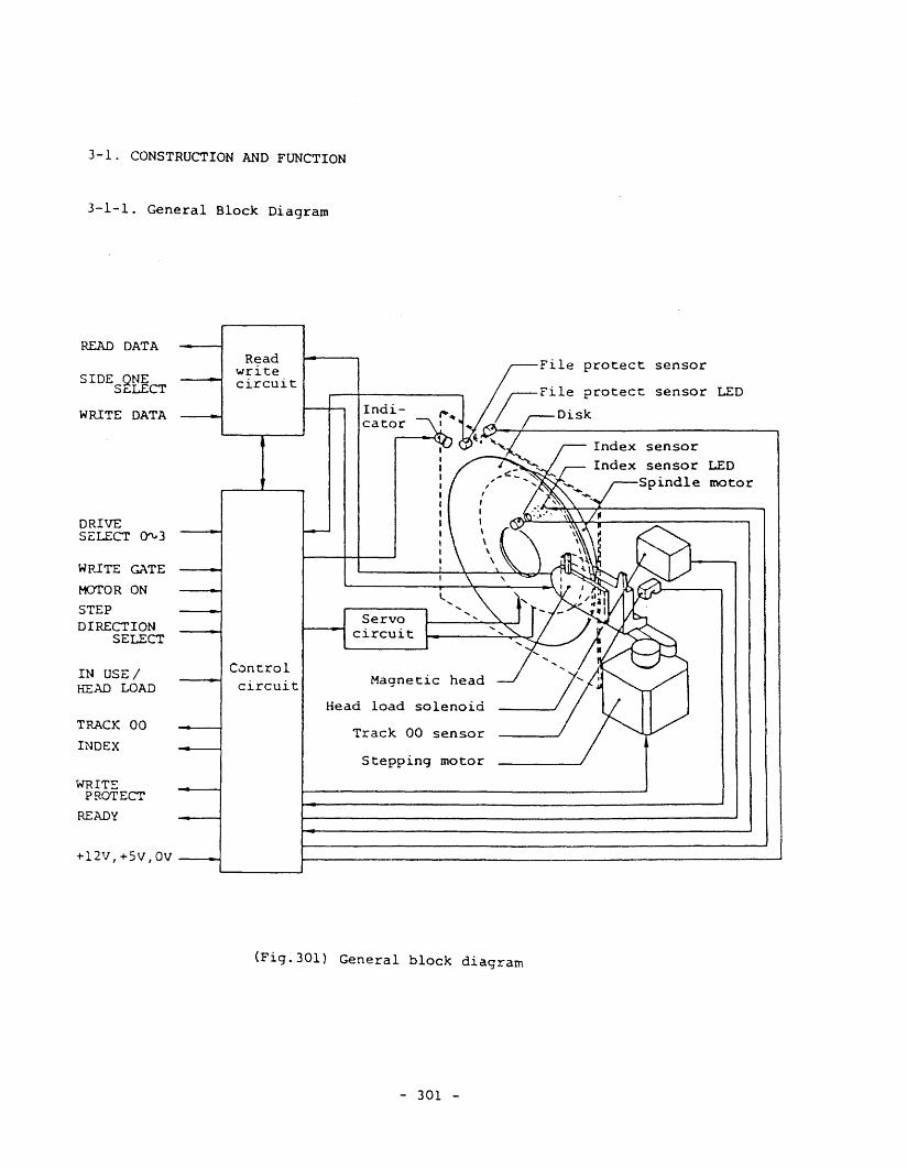
3-1. CONSTRUCTION AND FUNCTION
3-1-1. General Block Diagram
Readwritecircuit
READ DATA
SIDE QNESeLECT
WRITE DATA
DRIVESc.:LECT ()'\..3
WRITE GATE
MOTOR ON
STEPDIRECTION
SELECT
IN USc.: /HEAD LOAD
TRACK 00
INDEX
WRITEPROTECT
READY
+12V,+SV,OV
Cunt.rolcircuit
Indicator
Servocircuit
Magnetic head
Head load solenoid
Track 00 sensor
Stepping motor
File protect sensor
sensor LED
Index sensorIndex sensor LED
Spindle motor
(Fig.30l) General block diagram
- 301 -
3-1-2. Mechanical Section
Since the disk is a flexible recording media made of mylar film base
and data interchangeability between disks and FDDs is required, the
mechanical section of the FDD uses precision parts and it is also
assembled carefully and precisely. For this reason, only trained
technicians can handle the internal mechanism. Never apply excessive
impact nor drop the FDD down on the desk.
The mechanical section is constructed with frame, door mechanism, disk
clamp mechanism, disk rotation mechanism, magnetic head and carriage,
head load mechanism (or CSS mechanism), head seek mechanism, various
detection mechanisms, etc.
(1) Frame
The main structure for mounting the various mechanisms and printed
circuit boards. The frame is made of aluminum diecast to maintain
the stability of the FDD in strength, precision, durability, and
expansion coefficient.
(2) Door mechanism and disk clamp mechanism
The door mechanism is constructed with the main parts of set arm which
forms the structure for installing the disk on the spindle; other parts
of front lever, clamp arm, etc. The set arm is attached to the rear
of the frame with leaf spring and on the tip of the set arm a collet,
which forms the disk clamp mechanism, is attached.
When a disk is inserted and the door is closed, the collet is
inserted into the center hole of the disk and the disk is clamped in
the correct position along the outer circumference of the collet.
(3) Disk rotation mechanism
The disk rotation mechanism comprises DO motor Ass'y which includes
- 302 -
spindle.
The DO motor is an outor-rotor type DC brushless motor which has the
long life of 30,000 hours or more in continuous rotation.
The rotation speed is 300rpm for A ~ F models or 360rpm for G model
and is maintained at a stable condition against load variations and
environmental changes. This is achieved by a feedback signal from the
internal AC tachometer.
The collet and the spindle are combined precisely to maintain the
center position correctly without damaging the center hole of a disk
and so as to make the head be in contact with the disk at a correct
position.
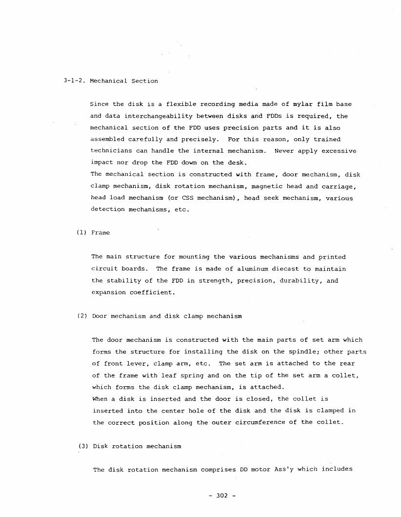
(4) Magnetic head and carriage
Read/wri te core
gaps
___ Rota tional directionof disk
Erase cores
(Fig.302) External view of magnetic head core
The magnetic head assembly (head carriage Ass'y) of a single sided
model (A or E model) is button type, which is mounted on the carriage
to be in contact with the head window area of the side 0 surface of a
disk (down surface when the FDD is situated horizontally). For a
double sided model (B, F, or G model), both of the side 1 head and
the side 0 head are special flat type supported with the gimbaled
mechanisms. The two magnp.tic heads are mounted accross the disk on one
carriage (head carriage).
In both types of head, the surface is designed for iltinimWii disk wear
and maximum read output. The head itself is a long life type for
improved head wear. Each head is constructed with a read/write gap
- 303 -
used for data reading and data writing and two erase gaps to erase the
recorded track edge immediately after the recordinCJ (tunnel erase).
The magnetic ehad and the carriage form the core section of the FDD
and is specially assembled with high precision.
(5) Head load mechanism or CSS mechanism
The head load mechanism is used for models with head load solenoid and
the CSS mechanism is used for double sided CSS model without head load
solenoid.
The head load mechanism functions to make the head in contact with a
disk when only required so as to reduce disk and magnetic head wear.
This mechanism is constructed with head load solenoid, arm lifter, etc.
If the head loading is executed for a single sided model, the head pad
attached to the pad arm of the carriage is depressed lightly against
the side 1 surface of a disk.
For a double sided model, the side 1 head attached to the upper arm of
the carriage is depressed against the side 1 surface of a disk with an
appropriate pressure.
The side 0 surfaces of the head and the disk are set to the same height
and the depression of the side 1 head produces the stable contact
between the heads and the disk.
In the CSS model, the magnetic heads are always in contact with a
disk as far as the disk is installed. In order to elongate the disk
and head leves, it is required to make the disk rotate only when it is
necessary.
The CSS mechanism is constructed with a CSS ASs'y which is designed
to protect the contact of side 0 and side 1 heads directly when the
front lever is closed without disk. For the purpose os protecting the
head being caught and damaged by the head window edge during disk
insertion and ejection, head protector is also equipped to the CSS
mechanism to lift up the disk jacket. The head protector is also used
- 304 -
in models with head load solenoid.
(6) Head seek mechanism
The head seek mechanism consists mainly of stepping motor with a capstan
(pooly), steel belt (band), and guide shafts. The head carriage is
connected to the capstan of the stepping motor through the steel belt
and is slided along the guide shafts.
The stepping motor rotates 2 steps (3.6°) in 48tpi models and I step
(1.8°) in 96tpi models for one track space. In some 48tpi models,
the stepping motor rotates 3.6 0 for one steps. For all models, hybrid
type 4-phase stepping motor is adopted to improve speed of the head
seek operation and precision of the head positioning. This special
motor is driven in a unique manner which brought a success in reducing
the heat radiation and to obtain a highly precise positioning.
The parallelism and the distance between the shafts and the center
line of a disk, and shafts and capstan themselves are precisely machined.
Also the thermal expansion of the frame, steel belt, carriage, etc. are
taken into consideration in the process of design so that they are
mutually offset with the expansion of the disk.
(7) Detection mechanisms
(a) File protect detection mechanism
This mechanism is constructed with an LED and a photo-transistor to
detect the existence of the write enable notch of the disk jacket.
When a disk with the notch covered is installed and the light pass
for detection is disturbed, no write or erase current will be supplied
to the read/write and erase heads and the recorded information on the
disk is protected from an erroneous input of a write command.
The LED is mounted on the PCBA DD motor servo and the photo-transistor
on the PCBA front OPT #H.
- 305 -
(b) Track 00 detection mechanism
This mechanism is constructed with a photo-interrupter for detecting
the'outermost track position (track 00) of the head and with a track
00 stopper which are attached to the rear side of the head carriage.
Inside tracks from the track 00 on the disk are used. Even if an
erroneous step out command is input from the track 00 position, the
command will be ignored by the internal circuit of the FDD.
If the head moves out from the track 00 by some reason (such as
impact during transportation), the head carriage strikes the track 00
stopper to protect the head from moving out of the returnable range
at a next power on. If V-type carriage is used (refer to Note 12 of
item 5-2-1 and Table 505), the frame edge functions like a track 00
stopper. And if L-type carriage (refer to Table 504) is used, a
screwed small parts functions as a track 00 stopper.
When step-in commands are input frOIn the innermost track, the head
moves toward inward with an appropriate space left against
the head window edge of the disk. In order to recalibrate the track
from this position (returning operation to the track 00), it is
required to input the step-out commands with several additional steps
to the maximum track number.
(c) Index detection mechanism
LED and photo-transistor for detecting the index hole are located
at the index window area of the disk jacket.
The LED is mounted on the PCBA DD motor servo (in the rotor of spindle
motor) and the photo-transistor on the PCBA front OPT #H. The index
hole will be detected along the rotation of the disk.
- 306 -
3-2. CIRCUIT DESCRIPTIONS
The electronics of the FDD is constructed with three sections which are
read write circuit, control circuit, and servo circuit. Read write
circuit and control circuit are mounted on the PCBA MFD control #H, and
servo circuit is on the PCBA DD motor servo.
3-2-1. Read write Circuit
The read write circuit is constructed with mode selector, read circuit,
write circuit, low voltage sensor. They are mostly packed in a read
write LSI (bipolar LSI, U5).
Fig.303 shows the block diagram.
- 307 -
(Fig.303) Block diagram ofread write circuit ILOW PASS Fl:LTER
L4. L5. RA1L C1B. C29
SWITCH FILTER 1C30.C31.07. oa. U1 I~-l-RA-C-K---SW---IT-C-H-.-SF-----------
JTRACKSWI TCU
DVGG
lDeR
RDCR
DGND
LVGG
CD qpI r
OINV
os
= ..... 0 .- :: "tJ '0:»- "'0 0 n 0
G> '0 ,.., '< G> CD:x lJ'J z :x 0
" "- ,.. c::» :10 , -l." 0 ,.,., "'0V) -< c::
0 -l
= 0 := := ." n"'0 n 0
G> ,.., Cj) (j') CD z::x z :x :x -l
"- ..... ." :lC:10 » I 00 -0 ,...-< V)
0
II
ill DRIVESELECT
"'1"32 1,/1 -300_ 6
SIDE ONE READSELECT DATA
WG _..--J
EG -........-------'
1,/1-226WR I TEDATA
COMMON(CENTER lAP)
ERASE COIL
1,/9-12
RE AD WR I H r.nll
SIOEOHEAD
TP4 TPS
IGA JN SELEClOR IA5V'" ... IOJ. FF ERENT I ATOR IS4/55 A C17 C20/..). :; :; R~2. C32. L3. C35
'-----.·r-Cll---....C)-----cn-J >0 ." ." 0 0 0 ·0
~ ~ ~ . ~ ~ ~ :;; :;; :;; "?1 r0lLolJL.:.F~0 -..
rw r10l nh '8~ '7~ '6~ ,h ~.~ r9~ '2~ J, :h C25~TPe
~;J ~ I ~ ~ DIFOR'iOO ~ _ ~CT I VE rn-~~.C......I--...J 1
2 ~ T C24
~~-I"'n-=--_ r--__-:.R~W...:..1..:..0--fIool..ff3f---+ HE AO f--tl. PRE. 0 J FFE RENH AT OR 'I-~ CJ -: TP7
_ 8 L.::.:::. SW ITCH f--tl. AMP ~EAK / ..:uo....J......:....:...._--S-y-6---4Ib-'r----v-- R"'01 -IT!f---+ MATRIX V =:E. .' ETECTOR At ,... 10 R"'11 r-:-=- LOW VOLTAGE SENSOR
'---.-'-----~ .....J-=-..:;..--4---. 1r----~...:..:..-..l{I[~ DV GG LVsol LV S1 tiil .....- ---.~---4~~ oY~~ EVCC I I TIME t'acP~~ WT r-:-=- r ~ DOMAIN ~ l'ME CONSTAllT
--...r- -L1l. I WR J TE l~ I'-J"r I F I LTER ~ C21. C22. RAg
~ 'liT 18 '--- DRIVER ~l..!.£.. ~
,.. 9 COM 1 r;-;::::-SI ol-E1----~:r-t---+-.--H--~:::=.!.--I~.19 [It COMI.ION I tEJHEAD HJ,. EVCC ~ DR I Veil r J I ~
.....~ I ~£r"'lr ~" ~--++---=C~OM~O~r--' I 1
Crl3 ..; R12 ill t, WR llE '. I r- ~L_+----'\NvA\r-if-+-_~E:..!:::D~1--1mHERASE leuRRENT /I 'iR JTE CONlR 0L :1 ~14-=-:;;"'--+-......
DR J VEIl SOURCE lOG I C ~t , t t t IfR0 DR J VER r---r----'--,.-I-..-'-...---..---,
~~4U~D6@~~~~;D~~@~~~~~Rl1 OV ~ EGND I ..., -: « n « c: ,.., ~l.J) ,-, :llCI
....---J.\IV'I..--+-t- -.l 0 n n tn I 0 I I:;) C) I-" < LJo VI VI III~ 0
I' ----
~'--------.t IWRI1E CURRENT I OUTPUT~\1SY),lMETRY ADJUSTOR 5W J TCH TPc I' I DR I VERft Re. R9.Q1 ~
~, I ~-----
waCD
3-2-1-1. Mode selector
Mode selector is constructed with the switch filter and write current
switch, which are used only for 96tpi models.
Table 301 shows the switching condition of the read write circuit by
the track switch signal (SF signal in the schematic diagram) from the
control circuit.
(1) Switch filter
Switch filter is used only in G model and in optional F model for
eliminating the influence of saddle waveform (refer to Fig.304) at the
outer tracks. When the SF signal is HIGH level, the output of the NPN
transistors, Q7 and Q8 (includes resistors int~rnally) becomes LOW
level. Then the switch filter capacitors, C30 and C3l are activated to
increase the capacity of the low pass filter capacitor, C29. This state
is the On-state of the switch filter, and the cut-off frequency of the
low pass filter is set to low.
(2) Write current switch
Write current switch is used only in E, F, and G models and used for
making the write current in outer tracks (track 00 to track 43) higher
than in inner tracks (track 44 to track 79) to improve the over-write
(write 2F after IF write and measure the residual frequency components
of IF) and sholder characteristics.
Write current is supplied to the write driver by write current source
in the read write LSI, US. The supplied value from this current source
can be calculated from the following expression combining the external
resistors R9, R8, and Ql (ON at outer tracks) .
13.2 12.7 12 1Outer tracks: Iw=~ +~ - O. --- No.
- 309 -
13.2Inner tracks: Iw= ---- - 0.12 --- No.2
R9
(Reference)
Erase current is calculated from the following expression. Write
current is not switched depending on the tr~ck position.
Ie= 10.8 --- No.3Rll (or R12)
Models and track position
Switching item A,B (48tpi) E,F (96tpi) . G(96tpi,high density)all tracks Tr.00'V43 Tr.44'V79 Tr.0Q'V43 Tr.44'\.,79
SF signal...... . .....
H H L H L
Switch filter I No circuit ON OFF ON OFF
Write current sw. Constant No.1 No.2 No.1 No.2(Current exp.) No.2
Erase driver Constant + + + +(Current exp.) No.3
(Table 301) Switdhing function of mode selector for read write circuit
- 310 -
3-2-1-2. Read circuit
The read circuit consists of head matrix switch, pre-amplifier,
low pass filter, differentiation amplifier, peak detector, time domain
filter, and output driver. Main circuits are enclosed in the read
write LSI, US.
The minute voltage induced in read operation by the read/write head i·s
input to pre-amplifier via matrix switch for selecting side 0/1 heads.
The pre-amplifier has three gain setting terminals, GSa, GSI and GSC.
In A ~ F models, GSO-GSC is shorted to obtain the gain of 100 times,
while GSl-GSC is shorted in G model to obtain the gain of 200 times.
The pre-amp. output is supplied to the differentiation amplifier via\
the low pass filter and the switch filter to ~liminate undesirable high
frequency noises. The differentiation amplifier phase-shifts the peak
position of the reproduced waveform to zero cross point, and at the
same time, further amplifies the signal with the most appropriate
equalization. The peak detector constructed with a comparator converts
the differentiated output after passing through the coupling capacitors,
C24 and C25 into a ~quare wave.
The time domain filter eliminates a virtual pulse caused by the saddle
in the low frequency area (IF area, 62.5KHz for A ~ F models, 125KHz
for G model) at outer tracks. The time domain filter is constructed
with two edge detectors, delay single shot, read data latch, and data
single shot. Then the signal is output from the FDD through the RD
driver and the output driver.
In the RD driver (3-state output) of the read write LSI, US, there
are some gates. To the TDCR terminal for pulse width setting of delay
single shot m.v., control signal from the control circuit (OPEN/ROYO/
APS signal) is input in parallel. These control signals are different
depending on PCB issue numbers (A ~ 0, E, or F ~) and PDD models (PCBA
versions). Anyway, the FDD is so set that the RD terminal outputs
positive read pulses at read operation. Table 302 shows the control
function.
- 311 -
PCB Typical RD output control No positive pulse outputs on RDissue PCBA terminal at:No. Version TDCR orNV DS (RD output: LOW level)
A"'D -00 A"-'C OPEN H L During write operation(
-04 A"-'C (Internal control of LSI)
-14,A,B RDYO H L During write + Drive not-READY(RDYO:LOW)_.
E -08,B,C APS H L During write + During motor start--lOA ting (36O'V380ms after MON) + Head-lSA seek operation
F'V -OOD'\. OPEN H H The same as -0Qt\..04 of PCB issue~
-040'\. A"-'D.
-080'\. RDYO H H The same as -14 A"-'D of PCB issue-lOB"-' A"-'D.-14C'V-ISH""
Special RDYO APS H During write + Drive not-READY+ Head, seek operation.
(Table 302) RD output control of read write LSI'
- 312 -
Magnetizationon disk
Pre-amp.output(TP4)
Pre-amp.output(TP5)
Differentiationamp.output(TP7)
Differentiationamp. output (TP8)
----l-~~-+--~:__----::;~---J't"-__t'---..;::".""r;::::.__-2. 5V ,approx.
..L...--l-..:::::,.........--+--~::::..-----=::~---;f---'l~---::T'<::..---2 . 5V ,
approx.
2.5V,approx.
--..l:..-----¥:----I---~r-----)'--_4:___--_t_2. 5V,
approx.
Peak detectoroutput in us I~- L
(Fig.304) Read amplifier and peak detector waveforms
- 313 -
Virtual pulse (drop~in)
I
T n n LJLJl fL
I-H--A"'F models: Ills, approx. , G model: O.S\.ls,approx.
U U U LnJIJ LJ
RD output (US-33)
READ DATA (Jl-30)
Read data latchoutput in uS
Edge detector #2output in uS
Peak detectoroutput in US
Edge detector #1output in uS
Delay s.s.Q output in US
(Fig.30S) Time domain filter and read gate waveforms
- 314 -
3-2-1-3. Write circuit
The write circuit consists of write control logic, write current source,
write driver, erase driver, common driver, and etc. Most of the
circuits are enclosed in the read write LSI, US.
Common driver output terminals, COMO and COMl are connected to the
common terminals (center taps) of the side 0 and side 1 heads,
respectively. The outputs of the common driver are controlled by the
SIDE ONE SELECT (Sl) input signal, and write gate (WG)/erase gate (EG)
signals supplied through the write control logic. When the COMO or the
COMl is HIGH level (ll.sV, approx.), the power to the read circuit is
cut off in the read write LSI to inhibit the read operation.
Input signals IFDD operation Output voltage (approx. )
Sl WG EG I COMO COMl
H H H SIDE 0 read operation 2.7V OV
H I L - SIDE 0 write operation 11.sV OV
H - L SIDE 0 write operation 11.SV OV
L H H SIDE 1 read operation OV 2.7V
L L - SIDE 1 write operation OV 11.SV
L I - L I SIDE 1 write operation OV 11.sV
(Table 303) Common driver output
The EG signal supplied from the erase timer in the control circuit
changes to HIGH or LOW level with an appropriate time delay against the
WG signal (refer to Fig.306). Since the erase gaps locate about
O.8srnm (A ~ F models) or O.s8srnm (G model) backward and across the
read/write gap, it is necessary for the erase driver to delay the WG
signal so that the written data is completely trimmed by the erase head
(tunnel erase). The tunnel erase produces a guard band between the
tracks preventing deterioration of the SiN ratio resulting from a off
track (positioning error). It also ensures disk interchangeability.
- 315 -
The WRITE DATA input pulse is latched by the write data latch in the
write control logic. And appropriate write current from the write
current source is supplied to the read/write head by turning on and off
the two write drivers alternately.
WRITE GATE (Jl-24)
Erase-on Erase-offdelay delay
((,..
-~\
WG (US-29)
EG (TP2)
SIDE ONE SELECT,(Jl-J2)
(,~
L___L
WRITE DATA (Jl-22)
Write data latch
in uS
Write driver output(US-17,18,12tV1S)
Write current
Magnetization ondisk
Previous magnetization
(Fig.J06) Typical waveform of write circuit operation
- J16 -
3-2-1-4. Low voltage sensor
The low voltage sensor is equipped to protect the FDD from erroneous
operation due to the internal circuit construction of the FDD during
unstable state of the power voltage such as at power on or off. Two
sensors of LVSO and LVSl are equipped in the read write LSI, US.
LVSO monitors the +5V and +12V voltage supplied to the internal circuit
of the read write LSI. If the voltage is lower than 3.SV through 4.4V,
it supplies signals to inhibit the operation of the common driver,
write driver, erase driver, and write control logic in the LSI, which
protect the disk from an erroneous write or erroneous erase during
unstable state of the power voltage.
LVSl is equipped to generate LVS signal to be supplied to the control
circuit in item 3-2-2. As well as LVSO, it is activated in the range
of 3.SV through 4.4V. The monitored voltage by the LVSl is only +5v
connected to the LVGG terminal (pin 37) of the read write LSI. While
the LVS signal is LOW level, all the control circuits (mainly control
LSI, U3) are reset~
+sv power
LVS (US-32)
Power on
3.S'\.4.4V
Power off
-++-- 3 . 5'\.4 . 4V
(Fig.307) Typical waveform of low voltage sensor
- 317 -
3-2-1-5. Function and operating waveform of read write LSI terminals
Following shows the function of the read write LSI, US and typical
operation waveforms.
(1) Pre-amplifier
(a) RWOO (pin 12), RWOl (pin 14)
Terminals for side 0 head connection~
~IL5v,approx.
II. -I WRITE DATA interval
Side 0 write
(b) RWOl (pin 13), RWll (pin 15)
Terminals for side 1 head connection.
Ll11.sV,approx.
RITE DATA interval
Side 1 write
(c) GSC (pin II), GSO (pin 10), GSl (pin 9)
lSide 0 read: 2.7V, approx.
Side 1 write: OV, approx.
Side 1 read: OV, approx.
lSide 1 read: 2.7V, approx.
Side 0 write: OV, approx.
Side 0 read: OV, approx.
Setting terminals of pre-amplifier gain.
If GSC-GSO is shorted or connected with a capacitor, the differential
- 318 -
voltage gain of the pre-amplifier is increased to 100 times. Also
if GSC-GSI is shorted or connected with a capacitor, it becomes 200
times.
(d) PREO (pin 7, pin 6)
Differential output terminals of the pre-amplifier. The phase of
pins 6 and 7 are opposite each other. (Refer to Fig. 304) .
A /\.-7....,.,L-~......V----...e--~'- 2 . 7V , approx •
Read
(2) Differentiation amplifier
(a) DIFI (pin 5, pin 4)
---,------- 2.7V,approx.
Write
Differential input terminals to the differentiation amplifier.
The phase of pin 5 and 4 are opposite each other.
/"-.... •~» "'-7' ..... 2. SV, approx.
Read
(b) DIFC (pin 3, pin 2)
--------- 2. Sv ,approx.
Write
Time constant setting terminals of the differentiation amplifier.
The phase of pin 3 and 2 are opposite each other.
- 319 -
A A---O/,.L----.oo...:V,.--r----..:>o.,',.-- 1 . 1v, a pprox .
Read
(c) DIFO (pin 1, pin 44)
--------- 1. lV, approx,
write
Differential output terminals of the differentiation amplifier.
The phase of pin 1 and 44 are opposite each other.
Read
(d) CI (pin 43, pin 42)
2.7V,approx.
write
2.7V,approx.
Differential input terminal of the comparator (peak detector). The
phase of pin 43 and 42 are opposite each other.
fV\ fV\-j+---\W--+---\-\- 2 • 5V, approx.
Read
(3) Time domain filter
(a) TDCR (pin 40)
----------2.5V,approx.
write
Pulse width setting terminal of the delay single shot m.v. Some
models use this terminal for the inhibit gate of the RD pulse output.
While this terminal is forced to be LOW level, the delay single shot
- 320 -
do not operate and no RD pulse is output. Refer to Table 302.
1.5V,approx.
~ Delay single shotpulse width
Read
(b) RDCR (pin 39)
lWrite: 1.5V,approx.
Read inhibit: 0.7V,approx.
Pulse width setting terminal for the RD output pulse.
r-RD2V,approx.
pulse width
Read
(4) Write circuit
(a) COMO (pin 21), COMl (pin 19)
-------- 2V,approx.
write & read inhibit
Output terminals of the cornmon driver. Two terminals are equipped
for the side 0 and side 1 heads respectively.
Refer to tables 303 and 304 as to the output voltage at each
operating condition.
(b) EOO (pin 24), EOl (pin 22)
Output terminals of the erase driver which is constructed with open
collector NPN transistors. Two terminals are equipped. While the EG
input terminal is HIGH level, one of the drivers which is selected
- 321 -
by the CS input terminal turns on (becomes LOW).
Refer to Table 304.
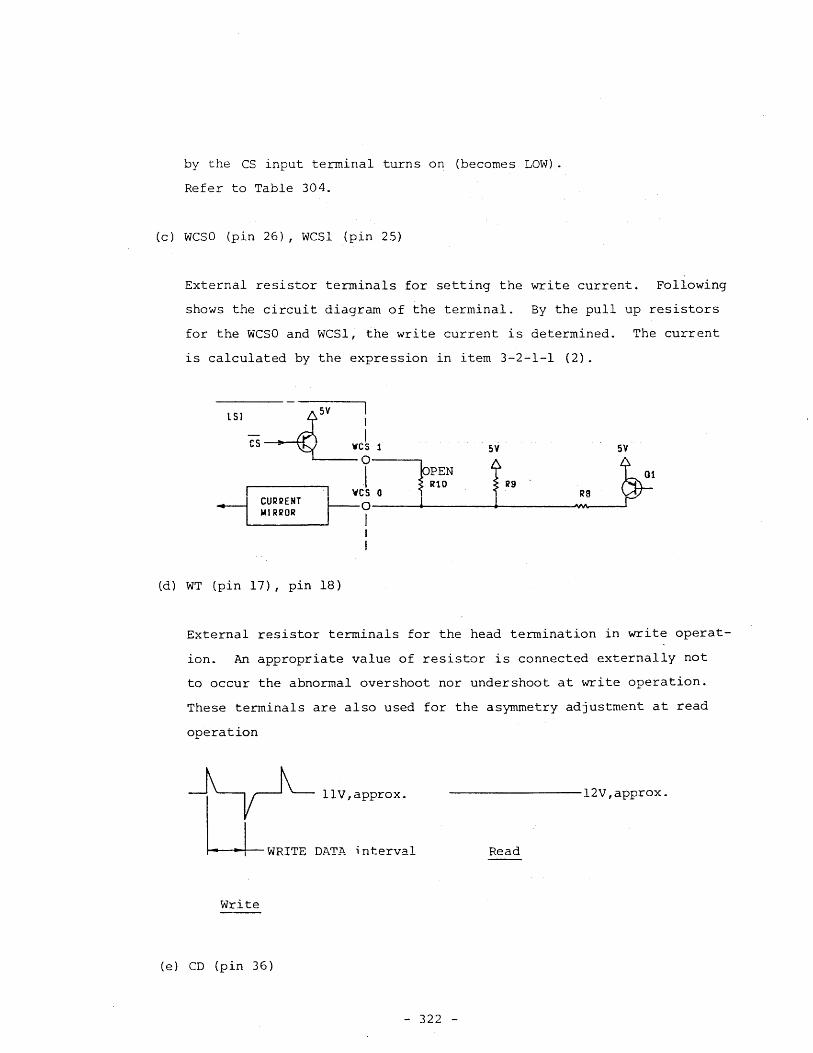
(c) WCSO (pin 26), WCSI (pin 25)
External resistor terminals for setting the write current. Following
shows the circuit diagram of the terminal. By the pull up resistors
for the WCSO and WCSl, the write current is determined. The current
is calculated by the expression in item 3-2-1-1 (2).
(d) WT (pin 17), pin 18)
External resistor terminals for the head tennination in write operat
ion. An appropriate value of resistor is connected externally not
to occur the abnormal overshoot nor undershoot at write operation.
These terminals are also used for the asymmetry adjustment at read
operation
llV,approx.
UWRITE DATA interval
Write
(e) CD (pin 36)
---------12V,approx.
Read
- 322 -
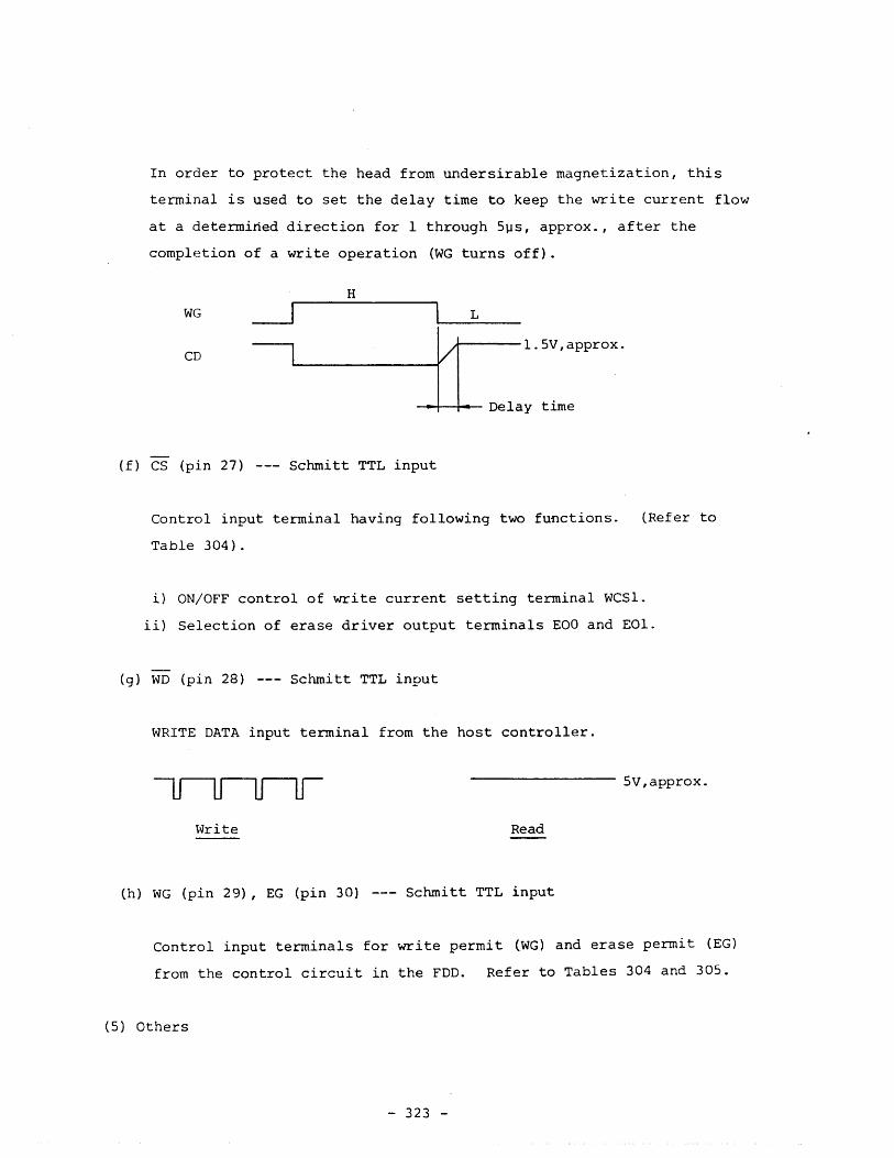
In order to protect the head from undersirable magnetization, this
terminal is used to set the delay time to keep the write current flow
at a determined direction for 1 through S~s, approx., after the
completion of a write operation (WG turns off).
H
WG
CD
~ I_L_1 $ 1.5V.approx.
JL Delay time
(f) CS (pin 27) --- Schmitt TTL input
Control input terminal having following two functions.
Table 304).
(Refer to
i) ON/OFF control of write current setting terminal WCSl.
ii) Selection of erase driver output terminals EOO and E01.
(g) WD (pin 28) --- Schmitt TTL input
WRITE DATA input terminal from the host controller.
~vri te
--------- SV,approx.
Read
(h) WG (pin 29), EG (pin 30) --- Schmitt TTL input
Control input terminals for write permit (WG) and erase permit (EG)
from the control circuit in the FDD. Refer to Tables 304 and 305.
(5) Others
- 323 -
(a) Sl (pin 31) --- Schmitt TTL input
SIDE ONE SELECT input terminal from the host controller.
The terminal functions as the selector for common driver outputs
COMO/COMl and for head switch matrix of RWOO,Ol/RW 10,11 terminals.
Refer to Table 304.
(b) LVS (pin 32) --- Open collector TTL output
LVS signal output terminal to the control circuit of the FDD. Refer
to item 3-2-1-4.
(e) OINV (pin 35), DS (pin 34) --- TTL input
Control input terminal of RD output. Refer to Tables 302 and
(d) AGND (pin 16), EGND (pin 23), and DGND (pin 38)
OV power terminals mainly for the following circuits in the LSI.
AGND: Analog operation circuits such as pre-amplifier.
EGND: Erase driver.
DGND: Digital operation circuits such as write control logic.
(e) AVGG (pin 8), DVGG (pin 41), LVGG (pin 37)
+5v power terminals mainly for the following circuits in the LSI.
AVGG: Analog operation circuits such as pre-amplifier.
AVGG: Digital operation circuits such as write control logic.
LVGG: Low voltage sensor (LVSl).
(f) EVCC (pin 20)
+12V power terminal.
- 324 -
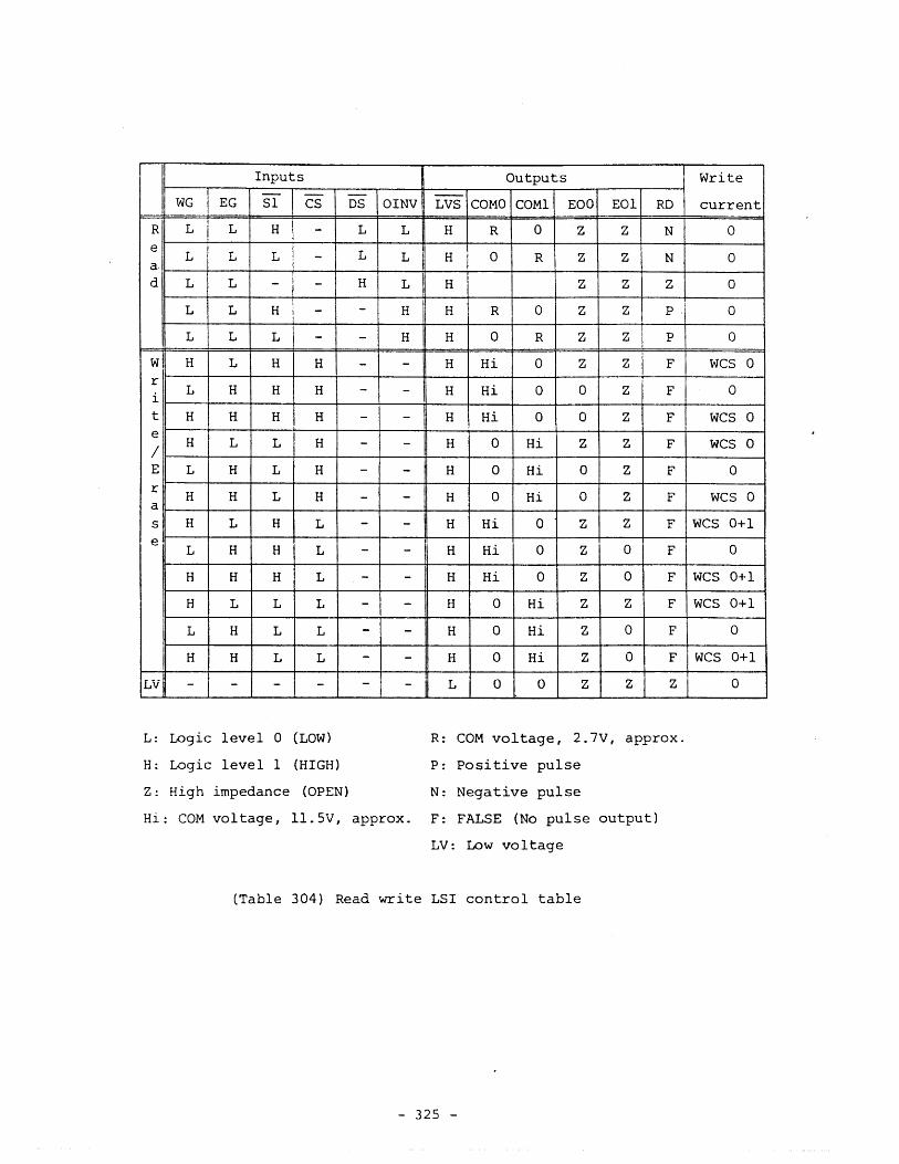
Inputs Outputs I Write- - - --WG EG Sl CS OS OINV LVS COMO COMl EOO EOl RD current
R L L H - L L H R 0 Z Z N 0e
L L L 0L - L H R Z Z N 0a·d L L - - H L H Z Z Z 0
L L H - - H H R 0 Z Z P ! 0
L L L - - H H 0 R Z Z P 0
W H L H H - - H Hi 0 z z F WCS 0ri
L H H H - - H Hi 0 0 Z F 0
t H H H H - - H Hi 0 0 Z F WCS 0e
/H L L H - - H 0 Hi Z Z F WCS 0
E L H L H - - H 0 Hi 0 Z F 0r
H H L H 0 Hi 0 Z 0- - H F WCSas H L H L - - H Hi 0 Z Z F WCS 0+1e I
L H H L - - H Hi 0 Z 0 F 0
H H H L - - H Hi 0 z 0 F WCS 0+1
H L L L - - H 0 Hi Z Z F WCS 0+1
L H L L - - H 0 Hi Z 0 F 0
H H L L - - H 0 Hi Z 0 F WCS 0+1
LV - - - - - - L 0 0 Z Z Z 0
L: Logic level 0 (LOW) R: COM voltage, 2.7V, approx.
H: Logic level 1 (HIGH) P: positive pulse
z: High impedance (OPEN) N: Negative pulse
Hi: COM voltage, ll.5V, approx. F: FALSE (No pulse output)
LV: Low voltage
(Table 304) Read write LSI control table
- 325 -

3-2-2. Control Circuit
The control circuit consists of strap circuit, LED & head load control
circuit, write/erase control circuit, motor on gate, ready detector,
stepping motor control circuit, track counter, disk change circuit,
interface driver, etc.
Almost all the circuits except for drivers are enclosed in the control
LSI, U3. Since the LSI is a CMOS type, input current is very small
(less than ±l~A) and a protective register is serially inserted in
the input terminal.
Fig.308 shows the block diagram.
- 326 -
SF
(Fig.308) Block diagramof control circuit
TO/FRO~ READ VRITE CIRCUIT/r-----------:.~-~:.......::...:....;,:...::...:...:.....:-------__.\.
ROYO APS VG EG LVS
FRONT LED
W10 STEP~.J
WRllE GAlE
MOTOR ON
INDElC
TRACK 00WRllE
PROTECTREADYIDISK CHANGE
l.40N1
l.40NO
DSEl
~I
ISTP
illDeDO
IDXO
TOO
WPO
RDYO
STRAPS ~--+-J
RY. XlLSIU3
CLOCK
I 1
CLOCKGENERATOR
STEPP I NGMOTOR
INDEXSENSOR---.
I
~.LEW
I
ov+
L : A.S MODEL(4BtDI)_H E'G MODEl(96tcl)
~ L : A'F MODELC300rorn)H G MODEl(360rorn)
L..-.._--=":...:'_-.=,3..0n ~C FOR SPINDLEMOTO~

3-2-2-1. Strap circuit
In order to select the various function by users, various strap
posts are available. Refer to the Specification items 1-11 and 1-12
as .to the details of strap function.
Some models have not strap posts. These models have soldered jumping
wires instead of the strap posts, and ~~e function is fixed. (Refer
to the version table in the schematic diagraml.
- 328 -
3-2-2-2. LED and head load control circuit
The circuits consists of LED/Head load gate, overdrive timer 1, LED
driver, solenoid driver, and overdrive circuit 1.
(1) LED/Head load gate
To the LED/Head load gate in the control LSI, U3, DRIVE SELECT (DSEL)
and IN USE (IU}/HEAD LOAD (IHL) signals are input.
According to the selected function designated by the straps Ul (USI
signal) and U2 (US2 signal), these input signals are gated to output
to the LED driver and the solenoid driver as OLEO and HLC signals.
(a) DLED signal
A signal to turn on the front bezel indicator (LED).
While this signal is LOW level, the LED turns on.
Strap setting U3 input LED on condition (OLEO LOW)
Ul U2 USI US2(No ~elation to HL strap & IHL input)
- --OFF OFF L L IU (L) + OSEL (L)
- --OFF ON L H IU (L) + OSEL (L)
ON OFF H L IU (L)
ON ON H H IU (L) + DSEL (L) x ROYa (H)
RDYO: U3, Ready detector output signal. HIGH in ready.
(Table 305) LED turn-on condition
(b) HLC signal
A signal to activate the solenoid for the models with head load
solenoid. While this signal is LOW level, the solenoid is activated.
- 329 -
Strap setting U3 input Solenoid on condition (HLS HIGH)-- (No relation to IU strap & IU input)
Ul U2 BL USl US2 IHL
OFF OFF OFF L L L DSEL (L) x PRDY --- No.1
OFF OFF ON L L L/H DSEL (L) x IHL (L) x PRDY --- No.2
OFF ON OFF L H L PRDY --- No.3--
OFF ON ON L H L/H IHL (L) x PRDY --- No.4
ON OFF OFF H L L The same as No.1
ON OFF ON H L LIB The same as No.2
ON ON OFF B H L The same as No.1
ON ON ON H H LIB The same as No.2
Note: PRDY= RDYO (see Table 305) + Pre-ready
Pre-ready: Internal signal of LSI. It becomes TRUE beforeone rotation of the disk (one INDEX pulse)
(Table 306) Solenoid drive condition
(2) LED driver
DLED signal from the control LSI, U3 is inverted and is input to the
driver IC, U7. U7 is constructed with NPN transistor array (open
collector output). Refer to Fig.309.
(3) Solenoid driver
The HLC signal from the control LSI, U3 with a pull up resistor of
lKQ is supplied to the driver IC, U7. Refer to Fig.309 as to the
construction of U7.
(4) Overdrive timer 1
The HLC signal is also supplied to the overdrive timer in the control
LSI. The overdrive timer is constructed with a retriggerable counter.
For the initial 26msec of the solenoid activation, it maintains the HOD
output (open drain) LOW level.
- 330 -
vee
IN
STB
-1.....1-...-0 CQA
OUT
20K
- - --M- - - +---......- .......-~- .......--n GHO
STa
IN 1 1
IN 2
IN 3 3
1N 4 4
IN 5 5
OUT 6J N 6
GNO
(Fig.309) Construction of driver IC, U7
(5) Overdrive circuit 1
The HOD signal is input to the PNP transistor Q5 which constructs the
overdrive circuit 1 and it makes Q5 turn on while the signal is LOW
level. +l2V power is applied to the solenoid at that time to execute
the drawing-in action of the solenoid securely.
After the overdrive period, the solenoid maintains its situation with
+5v power through the diode CRl to save the power.
In some models, overdrive function is not equipped with shorting the
emitter-collector of Q5. In such a model, +l2V is always supplied to
the solenoid.
- 331 -
HLC input
HOD output
Applied voltage
to solenoid coil
l 1~---------------12V' approx.
IJ
--_,-llv,approx., 4V,approx.I I ~----OV
~overdrive periodapprox.
(Fig.310) Overdrive timing of head load solenoid
- 332 -
3-2-2-3. Write/erase control circuit
The circuit consists of write/erase gate and erase timer. Most of the
parts of the circuit are enclosed in the control LSI, U3.
(1) Write/erase gate
The gate judges whether new data can be written on an installed disk.
If it can be, the circuit supplies the WG signal for the read write
LSI and erase timer.
The WG signal becomes TRUE in the followin~ condition. The conditions
are different depending on each LSI No.
(a) Control LSI No.: 2206-00 LHS060 or LHS060A
WG= DSEL(L) x IWG(L) x FPT(L) x MON delay 1 x SEEK
(b) Control LSI: 2206-00 LHS060B-- --
WG= DSEL(L} x IWG(L) x FPT(L)
Notes WG: Write operation at HIGH
DSEL: DRIVE SELECT input signal LOW.
IWG: WRITE GATE input signal LOW.
FPT: File protect sensor output (FPT input of LSI) LOW.
The same as that the file protect sensor detects the write
enable notch (light passing condition) of a disk which
is equivalent to that the WPO output of LSI is HIGH.
MaN delay 1: Internal signal of LSI. 360 ~ 380msec after a
motor-on command. Refer to Fig.31l.
SEEK: Internal signal of LSI. The ehad is not under seek
operation (not in 10 ~ 12msec for 96tpi and 13 ~ l5msec for
48tpi ~fter the last <::'!-o...-- ...--,,1<::0\---1:' J:""--~-' •
(2) Erase timer
- 333 -
The circuit to make the WG signal delay from the write/erase gate as in
Fig.306 to output the EG signal for the read write LSI. Refer to item
3-2-1-3.
Various delay time can be set by ERO ~ ER3 and SPED input terminals of
the control LSI. Only the SPED terminal is used for selection of the
FDD here.
U3 input terminals Erase delayFDD model
ERO ERI ER2 On-delay Off-delaySPED
A'\rF model H L L L 250~26711s 883~90011s
(300rpm)
G model H L L H 19l1\,200lis 54l~550lJs
(360rpm)
Note: The figure in the above table is the calculated valueexcluding the tolerance of the oscillator.
(Table 307) Erase delay control table
- 334 -
3-2-2-4. Motor on gate
The circuit, receiving a spindle motor-on command from the host
controller, supply the MC (motor control) signal to the spindle motor
servo circuit. The circuit consists of OR-gate, 123us delay circuit
and auto-turn circuit which are enclosed in the control LSI, U3.
A motor-on command input to the MONO or MONI terminal lS supplied to
123us delay circuit via the OR-gate to be delayed for 123 ~ 267us.
The delay circuit eliminates the noises mixed onto the interface line
and protects the control circuit from erroneous operation.
The MC signal becomes TRUE in the following conditions.
MC=(MONO(L) + MONl(L» x 123us delay x DISK
Notes MC: Motor rotation at HIGH
MONO: MOTOR ON input signal LOW
MONl: Differs depending on PCB issue.
Issue A ~ E: Fixed at FALSE (HIGH)
Issue F ~ DLED is low at ML strap is ON.
(Front bezel indicator is ON).
DISK: Normally fixed to TRUE (HIGH).
For optional FDDs with disk sensor, it becomes HIGH when
a disk is inserted.
The auto-turn circuit makes the spindle motor rotates automatically at
a disk insertion to improve the chucking accuracy. The circuit is set
by the information of a disk insertion from the disk sensor and file
protect sensor, and is reset at the detection of a ready state or more
than 10 seconds after the insertion. Even though the FDD becomes ready
state by a command from this circuit, the RDYO signal in item 3-2-2-5
mai~tai~s ~ALSE (LOW level) .
- 335 -
3-2-2-5. Ready detector
Ready' detect6r consists of 50% speed detector, ±6% speed detector,
pre-ready latch, ready latch, MON delay circuit which are enclosed in
the LSI, U3. In the block diagram, these circuits are shown as one
block of ready detector.
The Me signal for controlling the spindle motor is input to the ready
detector which enables the operation of all the above five circuits.
As the motor speed increases, 50% speed detector operates first, and
then pre-ready latch is set when the pulse interval becomes less than
twice of the nominal condition (i.e., 50% of disk speed). Then ±6%
speed detector starts its operation and sets the ready latch when the
pulse interval at the IDXS terminal becomes within ±6% of the nominal
condition. The ready latch is set when more than three index pulses
are detected after the motor start. In the typical case, the motor
speed reaches within ±6% of the rated speed when the next pulse is
detected after the pre-ready state. The ready latch will be set at
that time.
Operation modes of the two speed detectors are changed by the SPED
signal and the index pulse interval will be detected appropriately
for 360rpm (A ~ F models) or 300rpm (G model) .
On the other hand, the MON delay circuit generates two delay signals
after the MC signal becomes TRUE. One of them is the MON delay 1
signal to be supplied to write/erase gate (360 ~ 380msec delay) and
the other is the MON delay 2 signal (380 ~ 400msec delay). The MON
delay 2 signal and the ready latch output coinciding through AND gate
are output from the control LSI as the RDYO signal which indicates that
the FDD is read/write ready state. Fig.3ll shows the timing chart of
ready detector. The RDYO signal goes TRUE in the following conditions.
RDYO = MC x ±6% speed x MON delay 2
Notes RDYO: Ready at HIGH
- 336 -
MC: MC signal to the spindle motor HIGH (motor rotates).
±6% speed: IDXS pulse interval is within ±6% of nominal value.
MON delay 2: 380 ~ 400ms after MC signal becomes HIGH.
MC (Motor on command) --I
400ms Max.
Ready
Pre-ready
Constant speed
t±6%
Max.
360rpm: l66.7ms t300rpm: 200ms I~.~~--~
...-----.....
2t
380~40Oms
36O'V380m
360rpm: 73Oms, Max.300rpm: 800ms Max.
RDYO output
MON delay 1 in U3
MON delay 2 in U3
Ready latch in U3
50% speed detectionin U3
Pre-ready latchin U3
Disk rotation speed
IOXS (TPl)(Index detection)
IOXO output
Motor on I Head load enablet7:ith solenoid model)
Note: 300rpm: A~F models, 360rpm: G model
(Fig.3ll) Ready detector waveforms
- 337 -

All the five parts of ready detector are reset by the Me signal going
FALSE (LOW level) .
- 338 -
3-2-2-6. Stepping motor control circuit
Stepping motor control circuit consists of direction latch, internal
step generator, shift register, phase drive selector, overdrive timer,
coil driver, and overdrive circuit.
All the above circuits except for the coil driver and overdrive circuit
are enclosed in the control LSI, U3. In the block diagram, all the
enclosed circuit in the control LSI except for the overdrive timer are
shown as one block of the stepper control circuit.
(I) Direction latch
At every input of the STEP (ISTP) pulse from the host controller, the
direction latch samples and holds the head seek 'direction designated
by the DIRECTION SELECT (IDIR) signal. The latched output is supplied
to the bi-directional shift register and changes the activating order
of the stepping motor coil as shown in Fig.312.
(2) Internal step generator
The circuit has following purposes.
(a) The circuit generates an internal step pulse 3msec approx. later from
the STEP (ISTP) input pulse. This function is executed only when
the signal level at the TRK terminal is LOW (48tpi mode). When the
TRK is HIGH (96tpi mode or 48tpi mode with a stepping motor of 3.6°
for one step), it is not executed.
'When the TRK is HIGH level, the stepping motor rotates for one step
space in response to one STEP pulse. When it is LOW level, the stepping
motor rotates for two step space (3.6°) in response to one STEP pulse.
(b) When the RE strap for auto-recalibration is ON (PCB issue F and later)
and the control LSI No. is 2206-00 LHS060A or 5060B, step pulses for
- 339 -
auto-recalibration are generated at every 3msec 1 approx.
The auto-recalibration starts when the FDD is powered on and the LVS
signal from the read write LSI is changed from LOW to HIGH, and
continues until the detection of the track 00.
The maximum time required for auto-recalibration is 255msec.
During the execution of the auto-recalibration, the FDD maintains
NOT-ready state (RDYO output LOW) and the STEP (ISTP) pulse input
from the host controller is ignored.
(3) Shift register and phase drive selector
Step pulse and the output of the direction latch are supplied to the
shift register and the phase drive selector to be converted to the
appropriate timing signals for the uni-polar 1-2 phase drive of the
4-phase stepping motor. These phase drive signals are output from
the control LSI and supplied to the coil driver.
In order to improve the torque margin in the seek operation, partial
2-phase drive period is provided by the phase drive selector only in
the initial stage when the drive phase is changed. Refer to Fig.312
for timing chart.
(4) Coil driver
Four outputs, PA, PB, PNA, PNB from the control LSI, U3 are input to
the coil driver which consists of a driver Ie, U7. Refer to Fig.309
as to the construction of U7.
(5) Overdrive timer 2
External and internal step pulses are also supplied to the overdrive
timer 2 in the LSI. The overdrive timer 2 is constructed with a
retriggerable counter. During on-state of the timer (5Omsec; approx.) i
SOD output (open drain) from the LSI becomes LOW level. Refer to
Fig.313.
- 340 -
DIRECTION SELECT (Jl-18,IDIR) Step-outStep-in
PNB
_ --IJ__~_-....L__....L- ..L..-_-L.__i50ms .a~rox. .Internal step gen. in U3
. I s--JOverdrive operatlonL..--.+-+-----+------::.-----+-----i
PB
PNA
Coil driver input
PA
SOD (Overdrive timer 2)output
STEP (Jl-20,ISTP)
Direction latch in U3
96tpi (or 48tpi,3.6°):
tl t2
PNB
PB
PNB
SOD (Overdrive timer 2)output
Coil driver input
PA
48tP:~ternal step gen. in U3_~~-_·~+~--~~-~+-~a~~-I~~-~~(-~-;-s-:-~-~-~~r-o~x-)~~~_I~Oms::jprox.
14----+----+--+-----+--+----<r-I
tl tl
1"\' t2. . .11_ t2
tl: Internal step delay (3msec, approx.)t2: Partial 2-phase activating period (O.6ms,approx.)
(Fig.3l2) Stepping motor control circuit waveform
- 341 -
Final internal step pulse nin U3 ---J 1 _
SOD output T-'----__ 12V,approx.
Applied voltage to motorcoils
.. I I llV,approx.---.J .--- 4V,approx.
1------t-----OV
sOms, approx. ..1Overdrive period
(Fig.313) Stepping motor overdrive timing
(6) Overdrive circuit 2
The SOD signal is input to the PNP transistor Q6" which constructs the
overdrive circuit 2 and it makes Q6 turn on during LOW level. At that
time +12V power is applied to the stepping motor coils to execute
the seek and settling operations securely with high torque.
After the completion of the settling, only +SV power is supplied to the
coils through the diode, CR3 which minimize the power loss by supplying
only the required torque for holding the stop position. By the above
design, heat radiation is decreased to the minimum level and the power
consumption of the stepping motor in seek stop is only O.2SW, approx.
- 34~ ;,;.
3-2-2-7. Track counter
Track counter memorizes the track position and outputs track switch (SP)
signal for the read write circuit. It also outputs TOO (TRACK 00)
signal to the host controller. All the circuits are enclosed in the
control LSI, U3. The function of this circuit is used only in 96tpi
models. Refer to item 3-2-1-1.
The output signal from the track 00 sensor (TP3)is supplied to TOS
terminal of the LSI and is output as the TOO signal through the gate
in the track counter. The TOO signal becomes TRUE in the following
conditions.
TOO= TOS x Step out x PA
Notes TOO: Track 00 detected at HIGH.
TOS: Track 00 sensor output at TP3 (TOS input of LSI) is HIGH.
Track 00 sensor detects the light disturbing wing of the
head carriage (track 00 position) .
Step out: Direction latch output in item 3-2-2-6 is step-out
direction.
PA: PA output from stepping motor control circuit is HIGH.
Phase A coil of the motor is activated.
When the TOO signal becomes TRUE (HIGH level), the track counters
constructed from up-down counters are reset. If a step-in operation
is executed, the counter steps up and the SF output changes to LOW at
44th track. Refer to item 3-2-1-1 as to the function of the SF signal.
Track 00 ~ 43: SF signal HIGH.
Track 44 ~ 79: SF signal LOW.
~ 343 ~
3-2-2-8. Other terminals and function of control LSI
Following explains other terminals and function of the control LSI, U3.
(1) APS output terminal
APS signal becomes TRUE (HIGH level) in the following conditions.
The signal is used to inhibit the RD output pulse in some optional
models.
APS= MON delay 1 + SEEK
Notes MON delay 1: Internal signal of LSI. Spindle motor is under
starting operation. (See Fig.311).
SEEK: Internal signal of L~I. The head is under seek operation
(10 ~ 12msec for 96tpi and 13 ~ 15msecfor 48tpi after
the last step pulse) .
(2) OSCI, OSCO terminals and clock generator
It supplies clocks for operation to all the circuits in the LSI by
external ceramic oscillator.
(3) LVS input terminal
LVS signal input terminal from the read write LSI.
When it is LOW, all the circuits in the control LSI are reset.
(4) OINV input terminal
Terminal to invert the level of the control LSI output signals which
are used as output signals to the host controller. The terminal is
fixed to HIGH level in this FDD and HIGH output is TRL~_
(5) PSE 1 input terminal
- 344 -
Input terminal for power save control.
This function is not used in this FDD and it is fixed to HIGH level.
(6) SPC output terminal
Output terminal for power save control.
This function is not used in this FDD (open condition).
(7) MCK outputjRE input terminal
(a) LSI No. 2206-00 LH5060: MCK output terminal. Not used, open.
(b) LSI No. 2206-00 LH5060A or 5060B: RE input terminal
Execute auto-recalibration at LOW level.
(8) OCR, OCDO terminals and disk change circuit
Disk change circuit generates DISK CHANGE signal which indicates
that the disk is removed from the FDD. It is used only in some optional
models with disk sensor.
t"lhen a disk is removed, the DISK signal from the disk sensor becomes
LOW level and sets the flip-flop in the disk change circuit. This
is the disk change state and the neoo output becomes HIGH. If a disk
is inserted again and the OCR terminal is pulsed during the LOW level
of the OSEL (DRIVE SELECT) signal, the flip-flop is reset to make
the DCDO output return to LOW level. Since OCR terminal is connected
with ISTP terminal on the PCB, it is reset by the STEP pulse from the
host controller.
- 345 -
3-2-2-9. Interface driver
Output signals from the read write LSI and control LSI are supplied to
the host controller via the interface driver. AND gates of the inter
face driver makes these output signals to the host controller valid
only when the DRIVE SELECT input signal is TRUE (LOW level).
As to the INDEX and the READ DATA interface signals, there are some
types of output condition. In one of the types, signals from the LSI
are output as they are. In another type, they are output only when the
FDD is in ready state by means of ANDing with RDYO signal.
The interface driver used in this FDD differs as follows depending on
the PCB issue No. There are no difference in the construction of
open collector, sink current capability, and electric characteristics.
(a) PCB issue A ~ E: TTL7438
(b) PCB issue F and later: M52803 (Refer to Fig.3l4)
vee G2 6A 6Y 5A 5Y 4A oilY
G1 1A 1Y 2A 2Y 3A 3Y GND
(Fig.3l4) Construction of interface driver, M52803
- 346 -
3-2-3. Servo Circuit
There are two types of rotational speed which are 300rpm for A ~ F
models and 360rpm for G model. The start and stop of the rotation is
controlled by the MC signal through the motor on gate in the control
LSI.
The servo circuit aims to maintain the rotational speed of the spindle
motor at a determined constant speed, and the circuit is mounted on the
PCBA assembled with the spindle motor.
The spindle motor is a long life DC brushless motor having 3-phase coils
and bi-polar drive system. The coils are driven by the exclusive
servo IC. Energization and magnetized direction of the coils are
controlled by the signal from the hall elements.mounted on the servo
PCBA around the rotor so that they are changed corresponding to the
designated rotational direction.
The rotational speed is maintained stably and precisely. The feedback
signal from the AC tacho-meter in the rotor is converted into the drive
voltage (F-V conversion) by servo IC, and applied to the drive coils
through the phase compensation circuit.
Several manufacturers' spindle motors are sued in FD-55V series for the
stable supply of the motor. Though these motors are almost the same
in the function and performance, they are different in external view
because of a little difference in the servo circuit, etc.
- 347 -
3-3. FUNCTION OF TEST POINTS AND VARIABLE RESISTORS
Following shows the mounting position of the test points and variable
resistors.
GRl
Rl for asyrr~etry adjust
~~~~------+---T'Pl:IndexTP2: Erase GateTP3: Track 00TP4: Pre-amp.TP5: Pre-amp.TP6: DC OVTP7: DifferentiatorTP8: Differentiator
PCBA MFD control
version
~---PCBA revision
~------PCB issue
Dip side
Signal interface card edge
(Fig.3l5) Location of test points and variable resistors
348 -
3-3-1. Function of Test Points
Eight test points (one for ground) are equipped on the PCBA MFD control
#H for the check and adjustment of the waveforms of the FDD.
(1) TPl (Index)
Test point to observe the output of the index detection photo-transistor.
When the index hole is detected, LOW going pulse is observed.
The photo-transistor is mounted on the PCBA front OPT #H and the LED is
mounted on the DD motor (spindle motor) Ass'y.
The test point is used for the following purposes.
(a) Confirmation of the disk rotational speed.
(b) Rough confirmation and adjustment of the index burst detection timing.
Burst timing is adjusted by the fixing screws of the PCBA front OPT
#H. (Use INDEX interface signal for precise confirmation and
adjustment) .
. Pulse width
uII
• , i
uIndex
interval
TPI (Index)
(Fig.3l6) Typical waveform of TPl (Speed observation)
bll r ~ t del a y
TPl (Index)
TP4 or 5(Pre-amp. output)
IL....-- _
-+--vWNI. .[Index
17 'N'ave rorIll 'I'[' 1ubservaticn cf burst
... 349 -
TP2 (Erase gate)
ModelsItems
A"'F models G model
Index interval 200 ± 3ms 166.7 ± 2.5ms
Pulse width 2 '" 5.5ms 1 '" 8ms
Burst delay 200 ± 2001-ls 165 ± l651-1s
(Table 308) Index timing
(2) TP2 (Erase gate)
Test point to observe the output of the erase gate.
When TP2 is HIGH level, erase current flows through the erase head.
This TP is used for the check of the required delay time of the erase
gate signal against the WRITE GATE input signal:
WRITE GATE input signal ~'--------------
--;........I_l---+----LOn-delay U Off delay .1
(Fig.318) Typical waveform of TP2
ModelsDelay
A'VF models G model
On-delay 200 '" 3201-ls 175 '" 2l01-ls
Off-delay 860 '" 9501-ls 500 'V 5601-ls
(Table 309) Erase gate delay
(3) TP3 (Track 00 sensor)
Test point to observe the output of the track 00 detection photo-
- 350 -
transistor.
The signal level at this TP is opposite to that of the TRACK 00 output
signal. When the head is on track 00 or around track 00 position, TP3
becomes HIGH level.
The voltage of TP3 should be more than 4V at track 00 and less than O.SV
at track 04 (96tpi) or at track 02 (48tpi).
~~-------4.0V, Min.TP3 (Track 00 sensor)
------+---'----+----u. 5V, Max.
Track 04 (96tpi)
(Fig.3l9) Typical waveform of TP3
Track 00
Note: The TRACK 00 output signal goes TRUE (LOW level) only when the
phase A coil of the stepping motor is energized and the direction
latch is set to the step-out direction. Therefore, the level
change timing of the TRACK 00 signal is not consistent with that
of the TP3 signal.
(4) TP4, TP5 (Pre-amplifier)
Test point to observe the read pre-amplifier output signals.
The pre-amplifier has two outputs of the order of several dozen to
several hundred mVp-p, and they differ in phase by 180 0 (opposite phase) .
Both outputs are observed at TP4 and TPS respectively.
For an accurate observation of the read waveforms, use two channels of
an oscilloscope with one channel set to Invert mode and Add both
channels. Use TP6 (OV) test point for the oscilloscope ground.
TP4 and TP5 are used for checking various characteristics of the
read/write head and also for the check and adjustment of the head seek
mechanism such as track alignment.
- 351 -
TP4, TP5
(Pre-amp. )2.5V,approx.
(Fig.320) Typical waveform of TP4 and TP5
(5) TP7, TP8 (Differentiation amplifier)
Test points to observe the differentiation amplifier output signals.
Like the pre-amplifier, the differentiation amplifier also has two
outputs of the order of several hundred mVp-p to' several Vp-p which
differ in phase by 180°. Both outputs are observed at TP7 and TP8
respectively.
For an accurate observation of the waveforms, use two channels of the
oscilloscope with one channel set to Invert mode and Add both channels.
Use TP6 (OV) test point for the oscilloscope ground.
TP7 and TP8 are used for checking the total operation of the read/write
head and the read amplifier and for the check and adjustment of the head
seek mechanism such as track alignment.
TP7, TP8(Differentiator)
(Fig.32l) Typical waveform of TP7 and TP8
(6) TP6 (OV)
It is used as the ground terminal for measurement equipment. Be sure
- 352 -

to use a small size clip to obtain a probe ground of the
- 353 -
3-3-2. Function of Variable Resistor
On the PCBA MFD control #H, following variable resistor is mounted.
The variable resistor is correctly adjusted before the shipment of the
FDD and fundamentally it shall not be readjusted except for by a
trained technicians.
(1) Rl (for asymmetry adjustment)
Variable resistor for adjusting the asymmetry of the read data pulse.
Write IF data and observe the pulse intervals at the READ DATA output
line. Then adjust the variable resistor so that the read data as}~etry
takes the minimum value. Repeat each adjustment alternately for side 0
and side 1 heads to obtain the minimum asymmetry for both sides.
REl&J) DAT1'.
I 2 3r..--------.U u
IL Asymmetry 0
.IF interval. II 2 3
LJ-----,.t[li] U,..---
J-!!_._._A._Symml _e_t_r~v_A~F models: O.6~s,Max.
G model: O.3~s,Max.
Trigger
Note: When the READ DATA waveform is observed at theDOUT terminal of the SKA, positive going pulse isobserved.
(Fig.322) Read data asymmetry
- 354 -

SECTION 4
MAINTENANCE
- 4000 -
4-1. GENERAL
4-1-1. Periodic Maintenance
The FDD is designed to be free from periodic maintenance such as
replacement of parts, grease-up, etc. when it is operated at a ~ormal
operation duty.
However, cleaning of the magnetic head using a cleaning disk is
recommended since it is effective to improve the reliability of the data.
If some of the parts in the FDD are operated at a specially heavy duty
condition, or if the FDD is operated over 5 years, it is recommended
to replace the wear parts according to Table 510 in item 5-5.
Periodic maintenance items Recommended Required Referredcycle time items
Cleaning of magnetic head Refer to 4-3 5 min. 4-3-1,Replacement of wear parts Refer to 5-5 and 4-5.
(Table 401) Periodic maintenance items
- 4001 -
4-1-2. Check and Adjustment
.Table 402 shows all of the check and adjustment items.
Following items do not require periodic maintenance. Check and
adjustment should be done when required during replacement of the
maintenance parts or during trouble shooting referring to items 4-2
and 4-4.
The numbered procedure in Table 402 shows a typical procedure of the
general check and adjustment allover the FDD. After mechanical items
(steps 1 ~ 4), electric performance items (steps 5 ~ 15) should be
done.
Steps Check and adjustment items Required time Referred items
1 Adjustment of set arm position 5 minutes 4-4-1
2 . r'h.a ..... 1.r """"'~ adjustment of holder 5 minutes 4-4-2,-.A..a;~,-..n.. a.&..l\.l
position
3 Check and adjustment of arm lifter 5 minutes 4-4-3(Model with head load solenoid)
4 Check of CSS Ass'y (CSS model) 5 minutes 4-4-4
5 Check of file protect sensor 5 minutes 4-4-5·
6 Check of disk rotational speed 5 minutes 4-4-6
7 Check of erase gate delay 5 minutes 4-4-7
8 Check and adjustment of head touch 5 minutes 4-4-8
9 Check and adjustment of asymmetry 5 minutes 4-4-9
10 Check of read level 5 minutes 4-4-10
11 Check of resolution 5 minutes 4-4-11
12 Check and adjustment of track 10 minutes 4-4-12alignment
13 Check and adjustment of track 00 5 minutes 4-4-13sensor
14 Check and adjustment of track 00 5 minutes 4-4-14stopper
15 Check and adjustment of index 5 minutes 4-4-15burst timing
(Table 402) Check and adjustment items
- 4002 -
4-1-3. Maintenance Jigs and Tools
The following are the jigs and tools required for adequate maintenance
of the FDD.
(1) Equipment
(A) When the Simulator KA (off-line exerciser, abbreviated to SKA) is used:
(a) SKA
SKA Applied models
SKA-A 'V F FD-55AV "" FV
SKA-G (or SKA-GFII, G mode) FD-55GV
(Table 403) SKA and applied models
Notes: 1. Though SKA-A 'V F was simply called as SKA conventionally,
they are distinguished as SKA A 'V F here for convenience'
sake. However, when the identification of each SKA model is
not so important, all SKAs in table 403 are generally called
as SKA in the following explanation.
2. SKAs in Table 403 can be used also for FD-55(L) series.
(b) Accessories for SKA
SKA needs the following accessories for operating the FD-55V series.
The following accessories are common for all the v-series except for
special models.
i) SKA/FDD interface cable #0 (PIN 15922337-00)
ii) Check cable #5 (PIN 15922611-00)
SKA/FDD power cable is included in the check cable #5.
- 4003 -
Note: SKAs for FD-55(L) series differ from those for FD-5SV series
only in the check cable.
(c) Oscilloscope (two channels)
(d) DC power supply (+12V, 1.2A and +SV, 2A) or SKA power supply.
The following accessory is required for the power supply (The
accessory is supplied with the SKA power supply).
i) Power cable (4P)
(e) Thermometer and hygrometer
(B) When SKA is not used:
(a) FDD controller and DC power supply (user's system)
(b) Oscilloscope (two channels)
(c) Frequency counter
(d) DC clip-on ammeter
(e) Thermometer and hygrometer
(2) Tools
(a) Cross-point screwdrivers, M2.6 and M3
(b) Common screwdriver, small size
(c) Hexagon wrench key, l.Smm
(d) A pair of tweezers
(e) Round nose pliers
(f) Cutting pliers
(g) Solder and soldering iron
(h) Cutter knife
(3) Special jigs
- 4004 -
(a) Max. media jig for adjustment (~ig C, PIN 17890746-00)
(b) Max. media jig for check (Jig E, PIN 17890746-02)
(c) Alignment adjustment jig (PIN 17851100-00)
(4) Disks
(a) Work disk (commercially available disk)
i) For Normal density (FD-55AV ~ FV)
ii) For High density (FD-55GV)
(b) Cleaning disk (commercially available cleaning disk)
i) For single sided (FD-55AV, EV)
ii) For double sided (FD-55BV, FV, GV)
(c) Level disk
i) For Normal density (FD-55AV ~ FV), PIN 14900015-00
ii) For High density (FD-55GV), PIN 14900015-01
Note: Commercially available disks may be used if there is no doubt.
(d) Alignment disk
i) For single sided, 48tpi (FD-55AV) , PIN 14900016-00
ii) For double sided, 48tpi (FD-55BV) , PIN 14900016-21
iii) For single sided, 96tpi (FD-55EV), PIN 14900016-23
iv) For double sided, 96tpi (FD-55FV) , PIN 14900016-24
v) For High density, double sided, 96tpi (FD-:,SGV) , PIN 14900016-25
(5) Other articles used during maintenance
(a) Absolute alcohol (Ethanol)
- 4005 -
(b) Cotton swab or gauze
(c) Locking paint (Three Bond, 1401B)
(d) Screws and washers (Refer to item 5-2-2)
(e) Oil (Kantoh Kasei, FLOIL 464P, TEAC PIN 10854022)
(f) Grease (Kyodo Yushi, Mu1temp P2B, TEAC PIN 10857031)
Note: Be sure to use well calibrated equipment and disks.
- 4006 -
4-2. PRECAUTIONS
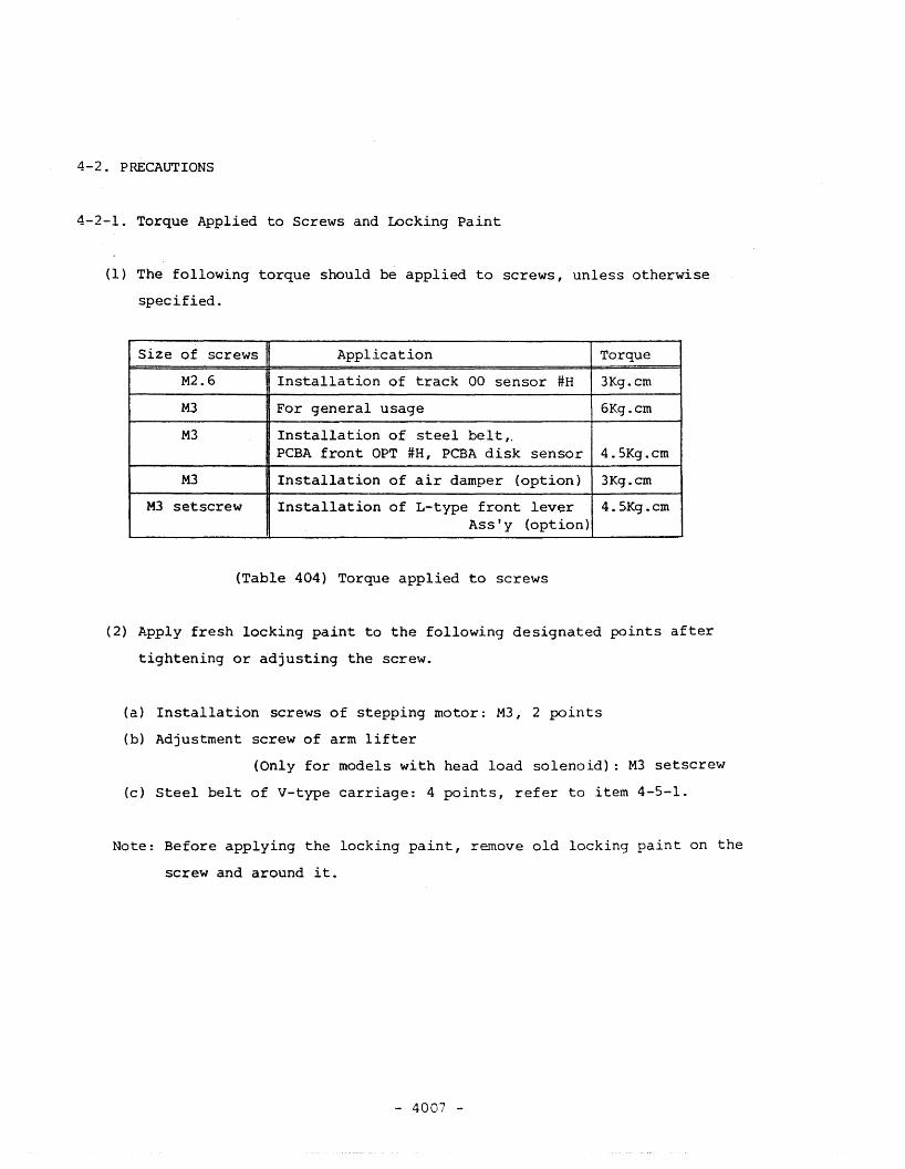
4-2-1. Torque Applied to Screws and Locking Paint
(1) The following torque should be applied to screws, unless otherwise
specified.
Size of screws Application Torque
M2.6 Installation of track 00 sensor #H 3Kg.cm
M3 For general usage 6Kg.cm
M3 Installation of steel belt,.PCBA front OPT #H, PCBA disk sensor 4.5Kg.cm
M3 Installation of air damper (option) 3Kg.cm
M3 setscrew Installation of L-type front lev~r 4.5Kg.cmAss'y (option)
(Table 404) Torque applied to screws
(2) Apply fresh locking paint to the following designated points after
tightening or adjusting the screw.
(a) Installation screws of stepping motor: M3, 2 points
(b) Adjustment screw of arm lifter
(Only for models with head load solenoid): M3 setscrew
(c) Steel belt of V-type carriage: 4 points, refer to item 4-5-1.
Note: Before applying the locking paint, remove old locking paint on the
screw and around it.
- 4007 -
4-2-2. Handling of Connectors
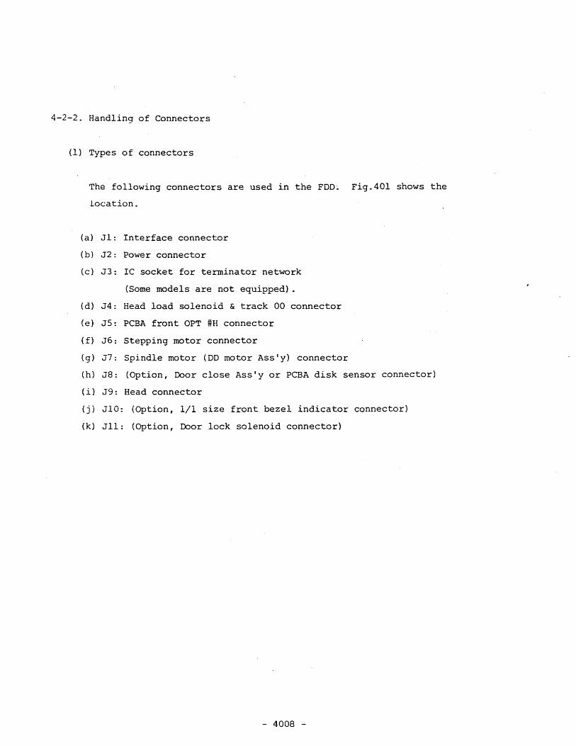
(1) Types of connectors
The following connectors are used in the FDD~ Fig.40l shows the
location.
(a) Jl: Interrace connector
(b) J2: Power connector
(c) J3: IC socket for terminator network
(Some models are not equipped) .
(d) J4: Head load solenoid & track 00 connector
(e) J5: PCBA front OPT #H connector
( f) J6: Stepping motor connector
(g) J7: Spindle motor (DD motor Ass' y) connector
(h) J8: (Option, Door close Ass'y or PCBA disk sensor connector)
(i) J9: Head connector
(j) JIG: (Option, 1/1 size front bezel indicator connector)
(k) Jll: (Option, Door lock solenoid connector)
- 4008 -
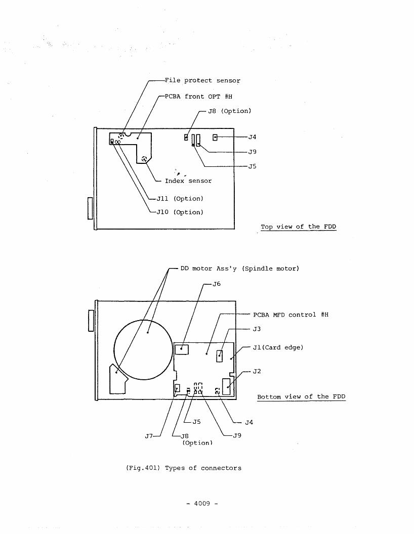
PCBA front OPT #H
F~le protect sensor
,......--+--J4
J8 (Option)
'------t-- J9
'-----+--J5
(Option)
(Option)
"
Index sensor
Top view of the FDD
motor Ass'y (Spindle motor)
~PCBA MFD control #H
J3
Jl(Card edge)
J2
Bottom view of the FDD
J4
J8(Option)
(Fig.40l) Types of connectors
- 4009 -
(2) Connection and disconnection of the connectors
Be sure to turn the power off before connecting and disconnecting the
connectors. Connection or disconnection should be done straightly and
correctly without applying excessive force to the cables and the post
pins.
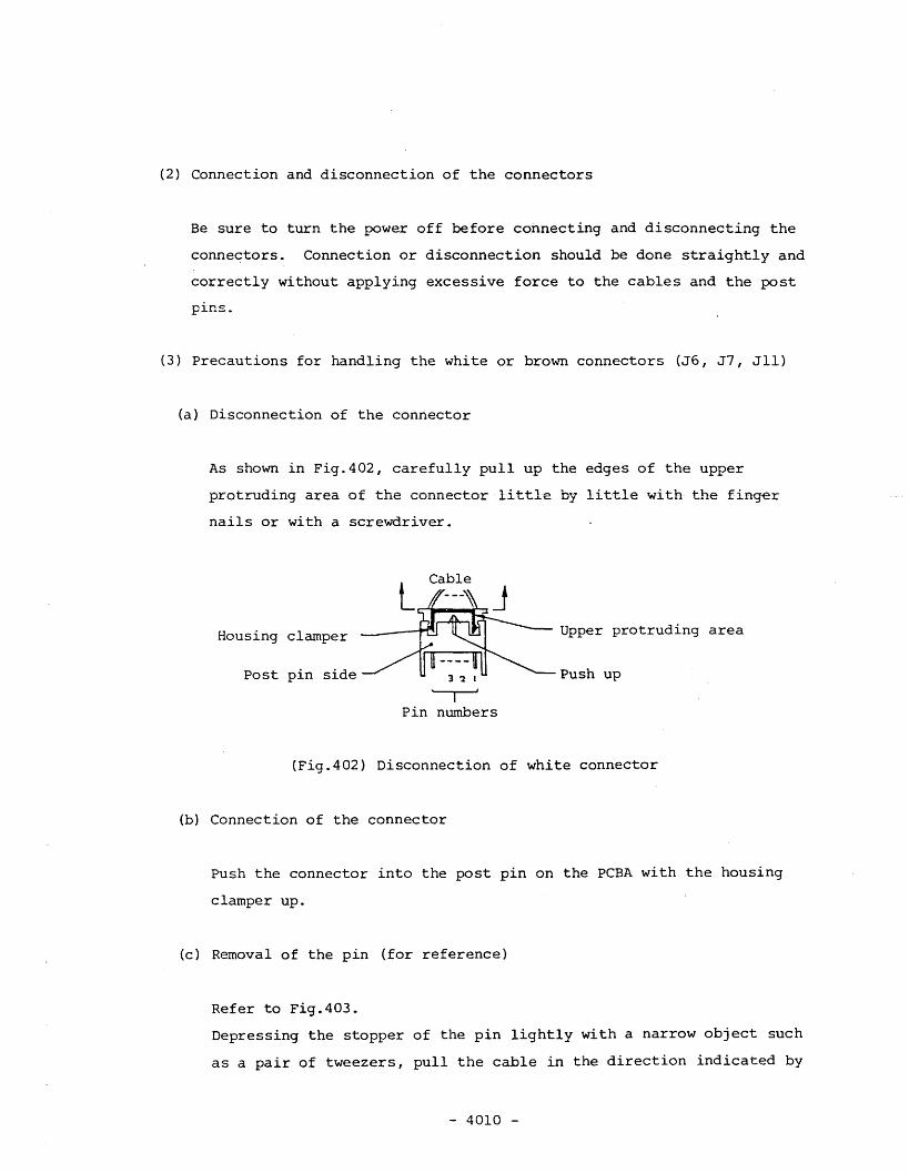
(3) Precautions for handling the white or brown connectors (J6, J7, JIl)
(a) Disconnection of the connector
As shown in Fig.402, carefully pull up the edges of the upper
protruding area of the connector little by little with the finger
nails or with a screwdriver.
Housing clamper
Post pin side
Cable
IPin numbers
Upper protruding area
Push up
(Fig.402) Disconnection of white connector
(b) Connection of the connector
Push the connector into the post pin on the PCBA with the housing
clamper up.
(c) Removal of the pin (for reference)
Refer to Fig.403.
Depressing the stopper of the pin lightly with a narrow object such
as a pair of tweezers, pull the cable in the direction indicated by
- 4010 -
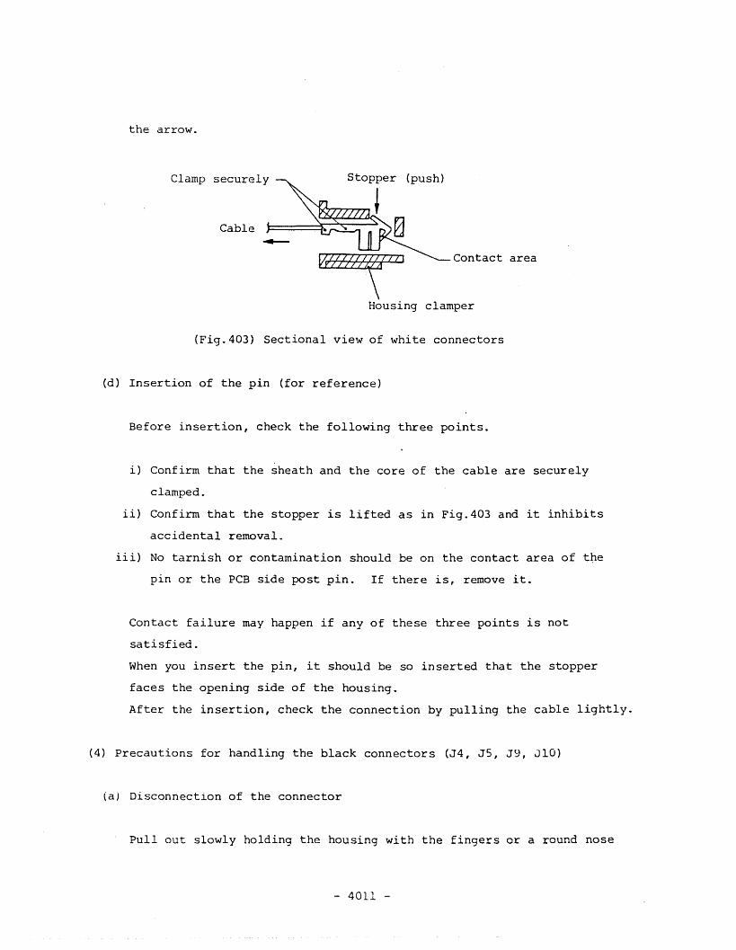
Contact area
the arrow.
Clamp securely
Cable
(push)
\Housing clamper
(Fig.403) Sectional view of white connectors
(d) Insertion of the pin (for reference)
Before insertion, check the following three points.
i} Confirm that the sheath and the core of the cable are securely
clamped.
ii) Confirm that the stopper is lifted as in Fig.403 and it inhibits
accidental removal.
iii} No tarnish or contamination should be on the contact area of t~e
pin or the PCB side post pin. If there is, remove it.
Contact failure may happen if any of these three points is not
satisfied.
When you insert the pin, it should be so inserted that the stopper
faces the opening side of the housing.
After the insertion, check the connection by pulling the cable lightly.
(4) Precautions for handling the black connectors (J4, J5, JY, JIO)
(a) Disconnection of the connector
Pullout slowly holding the housing with the fingers or a round nose
- 4011 -
pliers. Be sure not to apply tension to the fine cables of the J9
(head connector).
(b) Connection of the connector
Make the polarizing key position of the housing correspond with the
lack of the post pin, and push the housing carefully with the fingers.
(c) Removal of the pin
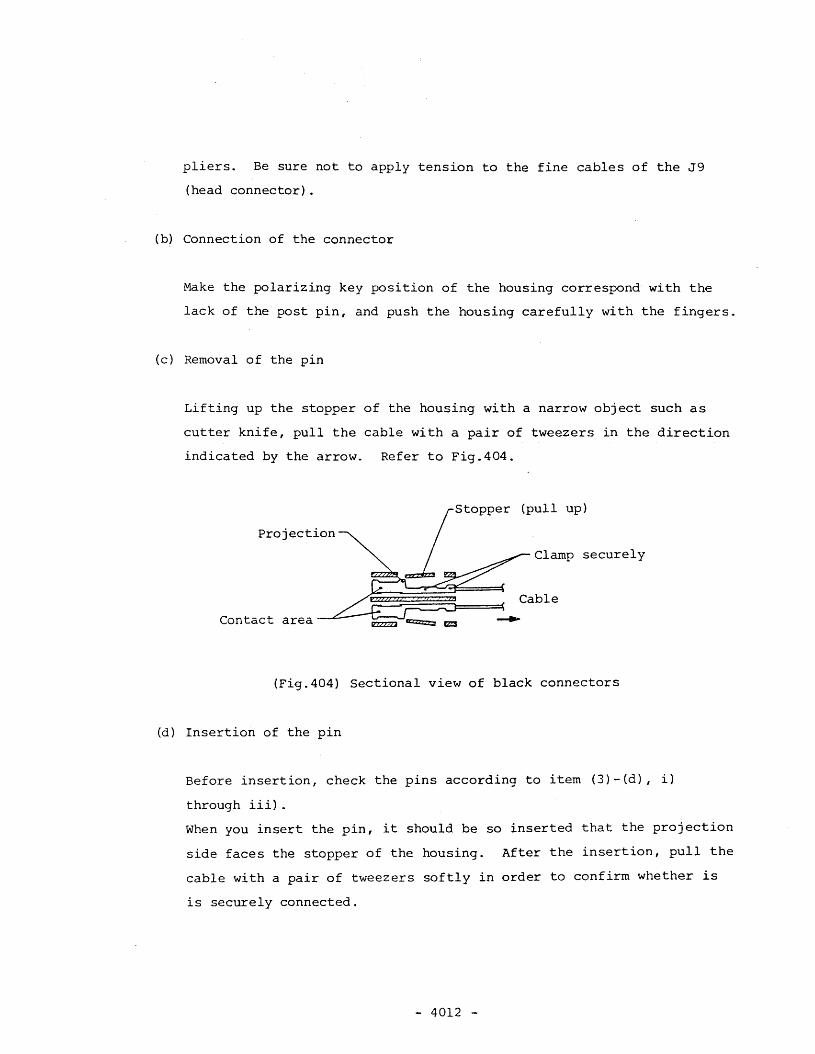
Lifting up the stopper of the housing with a narrow object such as
cutter knife, pull the cable with a pair of tweezers in the direction
indicated by the arrow. Refer to Fig.404.
Projection
Contact area
(pull up)
Clamp securely
Cable
----
(Fig.404) sectional view of black connectors
(d) Insertion of the pin
Before insertion, check the pins according to item (3)-(d), i)
through iii).
When you insert the pin, it should be so inserted that the projection
side faces the stopper of the housing. After the insertion, pull the
cable with a pair of tweezers softly in order to confirm whether is
is securely connected.
- 4012 -
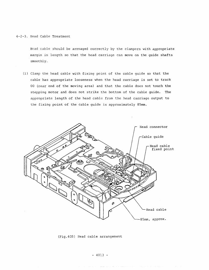
4-2-3. Head Cable Treatment
Head cable should be arrnaged correctly by the clampers with appropriate
margin in length so that the head carriage can move on the guide shafts
smoothly.
(1) Clamp the head cable with fixing point of the cable guide so that the
cable has appropriate looseness when the head carriage is set to track
00 (rear end of the moving area) and that the cable does not touch the
stepping motor and does not strike the bottom of the cable guide. The
appropriate length of the head cable from the head carriage output to
the fixing point of the cable guide is approximately 85mm.
Head connector
Cable guide
Head cablefixed point
cable
~85rnrn, approx.
(Fig.405) Head cable arrangement
- 4013 -

(2) Form the cable not to have excessive looseness in the area from the
head connector to the cable guide.
- 4014 -
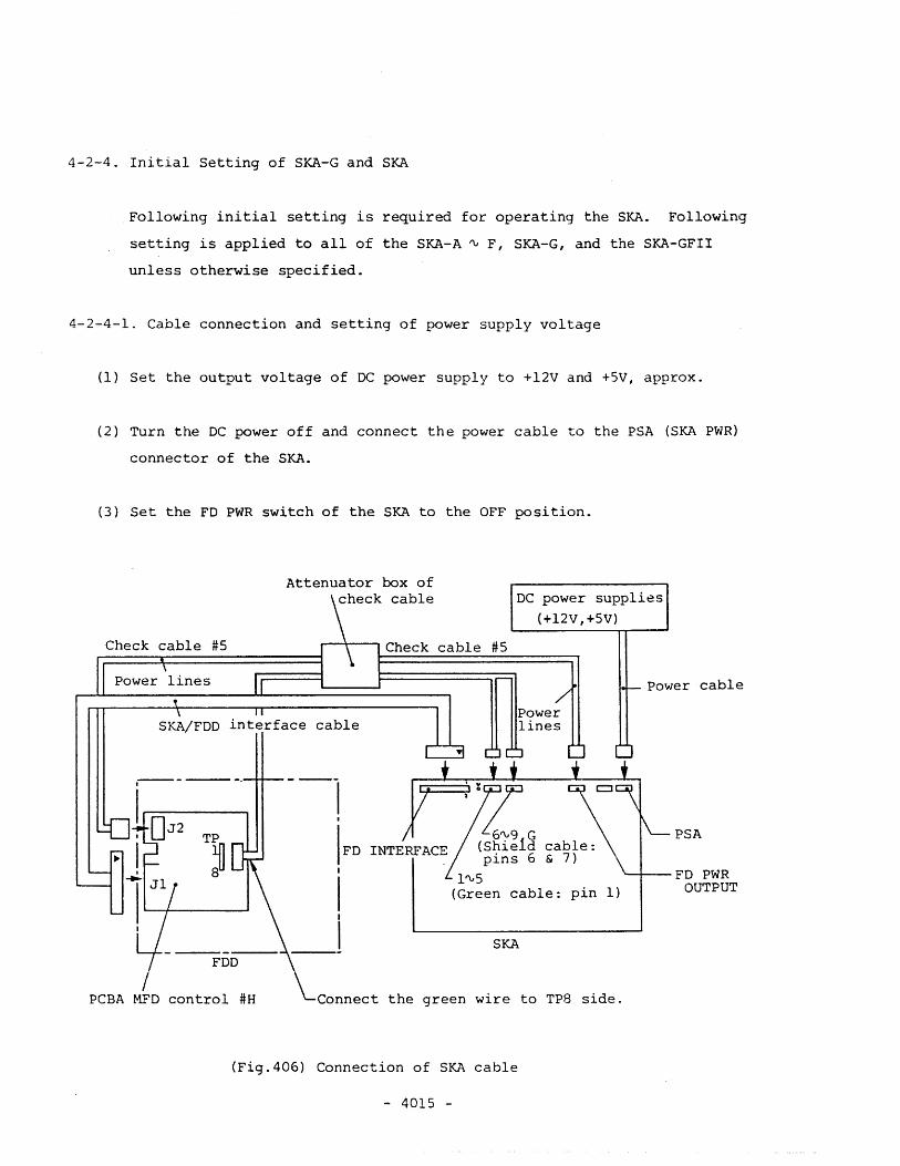
4-2-4. Initial Setting of SKA-G and SKA
Following initial setting is required for operating the SKA. Following
setting is applied to all of the SKA-A ~ F, SKA-G, and the SKA-GFII
unless otherwise specified.
4-2-4-1. Cable connection and setting of power supply voltage
(1) Set the output voltage of DC power supply to +12V and +5V, approx.
(2) Turn the DC power off and connect the power cable to the PSA (SKA PWR)
connector of the SKA.
(3) Set the FD PWR switch of the SKA to the OFF position.
PSA
'---+--- FD PWROUTPUTpin 1)
cable:& 7)
Power cable
DC power supplies(+12V,+5V)
SKA
Check cable #5
INTERFACE
Attenuator box ofcheck cable
--1I
IFDI
I_-4,_1
FDD
TP
~
SKA/FDD interface cable
Check cable #5
/PCBA MFD control #H Connect the green wire to TP8 side.
(Fig.406) Connection of SKA cable
- 4015 -
(4) Connect the SKA/FDD interface cable. Pay attention to the identificat
ion mark of the connector (6) so that it locates at the pin 1 and 2
side.
(S) Connect the FD PWR OUTPUT of the SKA and J2 of the FDD with the
power line of the check cable #S.
(6) Connect the black connector (8P) of the check cable #S to TP1 ~ TP8
of the FDD. Be sure to connect so that the green wire comes to TP8
side.
(7) Connect the white connector with shielded wire of the check cable #S
to terminals 6 ~ 9, G of the SKA. The shielded wire side comes to
terminals 6, 7 side of the SKA.
(8) Connect the white connector without shielded wire of the check cable #S
to terminals 1 ~ S of the SKA. Green wire side comes to terminal 1
side of the SKA.
(9) Turn the DC power on. Set the FD PWR switch of the SKA to the PSA side.
(10) Key in "CB If . (+SV VOLTAGE)
(11) Adjust the DC power voltage so that the DATA indicator of the SKA
I I J I I (V) indicates the value wi thin the range of S. OO± 0.1V.
(12) Key in IfF If . (STEP)
(13) Key in IfCC". (+12V VOLTAGE)
(14) Adjust the DC power voltage so that the DATA indicator
indicates the value within the range of l2.00±0.24V.
(IS) Key in IfF If . (STOP)
- 4016 -
I J I I (V)

Note: The above items (1), (2), (7), (8), (10) ~ (15) may be omitted
for replacement of the FDD or a temporary FDD power off. Remain the
DC power on for the SKA and control the FDD power by the SKA PWR
switch.
- 4017 -
4-2-4-2. Setting of the maximum track number
Before the check and the adjustment of the FOO, set t-he maximum track
number according to the following instructions.
The setting will be maintained until the main DC power (SKA PWR) is
turned off or until the RESET switch of the SKA is depressed. Since
the FO PWR switch is independent of this setting, it is convenient
to maintain the main DC power on for the successive operations.
The initial setting of the following is not required if the maximum
track number is the same as the initial value of the SKA.
(1) Key in "CF". (SET TMAX)
(2) The maximum track number set at that time is indicated with the latter
two digits of the DATA indicator I I I I I (track).
Note: If there is no change in the maximum track number in item (2),
depress "F" key.
(3) Key in the maximum track number used for the POD in two digits of
decimal notation.
e.g. 48tpi (FO-55AV, BV): CF 39 (for 40 cylinders)
96t~i (FD-55EV, FV): CF 79 (for 80 cylinders)
96tpi, high density (FO-55GV): CF 76 (for 77 cylinders)
Note: If 80 cylinders are used in FD-55GV, key in "CF 79" also for the
SKA (Key in "CF F" if it is the same as the initial value of the
SKA) .
- 4018 -
4-2-4-3. Setting of step rate and settling time
Before check and adjustment of.the FDD, set the step rate and the
settling time according to the following instructions.
The 'setting will be maintained until the main DC power (SKA PWR) is
turned off or until the RESET switch of the SKA is depressed.
If the step rate and the settling time are the same as the initial
values of the SKA, the initial setting of the following is not required.
(1) Key in "DB". (SET STEP RATE)
(2) Step rate set at that time is indicated by O.lmsec scale on the DATA
indicator I I I J I (ms).
e.g. DATA indicator It.-dOl indicates 6. Omsec.
(3) Key in a new step rate down to one decimal place (unit:msec).
Note: If there is no change in step rate in item (2), omit item (3) and
forward to item (4).
(4) Key in "F". (STOP -- Setting of the step rate completes).
(5) Settling time at that time is indicated by O.lmsec scale on the DATA
indicator I / I d / (ms).
e.g. DATA indicator 1//5101 indicates l5.Omsec
(6) Key in new settling time down to one decimal place (Unit: msec).
Note: If there is no change in settling time in item (5), omit item (6)
and depress "F" key to complete the operation.
- 4019 -

(7) Depress "F" key. (STOP -- Setting of the settling time completes).
e.g. 48tpi (Step rate 6msec, Settling time 15msec): DB 60 F 150 F
96tpi (Step rate 3msec, Settling time 15msec): DB 30 F 150 F
- 4020 -

4-2-4-4. Level disk calibration
Setting of the following calibration value is required for accurate
measurement before the check of the read level or the resolution.
Use a level disk with a calibration value (100% center) written on the
label. The setting will be maintained until the main DC power (SKA PWR)
is turned off or until the RESET switch of the SKA is depressed.
If the calibration value is the same as the initial value (100%) of the
SKA, the initial setting of the following is not required.
(1) Innermost track read level
(a) Key in "DO". (CALIBRATION READ LEVEL)
(b) Calibration value set at that time is indicated in the latter three
digits of the DATA indicator I I I I I (%).
(c) Key in a new calibration value written on the level disk label
(three digits, Max.).
(d) Key in "F". (STOP)
Note: If there is no calibration change in item (b), omit item (c) and
depress "F" key.
(2) Innermost track resolution
(a) Key in "01". (CALIBRATION RESOLUTION)
(b) Calibration value set at that time is indicated in the latter three
digits of the DATA indicator ~l~:~1~1~1 (%j.
(c) Key in a new calibration value written on the level disk label.
(three digits, Max.)
- 4021 -
(d) Key in "F". (STOP)
Note: If there is no calibration change in item (b), omit item (c) and
depress "F" key.
e.g. READ LEVEL 103%, RESOLUTION 96%: DO 103 F, Dl 96 F
Note: The setting in this item is not required when the level disk
is not used (i.e., when it is substituted with a commercially
available disk and no accurate measurement is required).
Calibration value should be the same as the initial value (lOO%).
- 4022 -
4-2-4-5. Alignment disk calibration
Setting of the following calibration value is required for accurate
measurement before the check and adjustment of the track alignment.
Use a correctly calibrated (0% center) alignment disk with a calibration
value written on the label. The setting will be maintained until
the main DC power (SKA PWR) is turned off or until the RESET switch of
the SKA is depressed.
If the calibration value is the same as the initial value (0%) of the
SKA, the initial setting of the following is not required.
(1) SIDE 0 alignment
(a) Key in "EO". (CALIBRATION SIDE 0 ALIGNMENT)
(b) The calibration value set at that time is indicated in the latter two
digi ts of the DATA indicator I I I I I (%), and the polarity is indicated
in the initial digit. If a "0" is indicated, the polarity is positive.
Polarity indication: plus I,- , minus
(c) Key in a polarity and a new calibration value (two digits, Max.)
written on the alignment disk label.
Designation of polarity: Depress "B" key only for minus designation.
(No designation is required for plus) .
(d) Key in "F". (STOP)
(2) Side I alignment
(a) Key in "El". (CALIBRATION SIDE I ALIGNMENT)
(b) The same as in item (l)-(b) ~ (d).
- 4023 -
INDEX output signal ~
Lobe pattern(TP7,8)
A B A B
Notes: 1. The lobe pattern ratio is calibrated in the SKA according to thefollowing expression.
. A-BLobe pattern ratlO= f x 100-Calibration value(%)
. . Larger one 0 A & Bafter callbratlon
2. If the calculated value with the above expression is positive,the polarity is plus, while the polarity is minus when thevalue is negative.
(Fig.407) Calibration of alignment lobe pattern
(3) Index burst timing
(a) Key in "E5". (CALIBRATION INDEX TIMING)
(b) The calibration value set at that time is indicated in the latter
three digits of the DATA indicator I I I I I (l1S), and the polarity is
indicated in the initial digit. (Refer to item (l)-(b)).
If a "0" is indicated, the polarity is positive.
(c) Key in a polarity and a new calibration value (three digits, Max.)
written on the alignment disk label. Refer to item (l)-(c) for the
polarity designation.
(d) Key in "F". (STOP)
Note: If there is no change in the calibration value in item (b), omit
item (c) and depress "F" key.
- 4024 -
e.g. Double sided FOO, SIDE 0 ALIGNMENT +3%, SIDE 1 ALIGNEMTN -5%,
INDEX TIMING -25~s:
EO 3 F, El B 5 F, E5 B 25 F
INDEX output signal
Index burst (TP4,5)
-11--~----------
~-,t"'--tl....-_ Index burst timing
Notes: 1. The index timing is calibrated in the SKA according to thefollowing expression.
Calibrated timing = t - calibration value {~s}
2. If the calculated value with the above expression ispositive, the polarity is plus, while the polarity is mlnuswhen the value is negative.
(Fig.40B) Calibration of index burst timing
- 4025 -
4-2-4-6. Humidity setting
For the check and adjustment of the track alignment using an alignment
disk, set the environmental relative humidity to the SKA in order to
improve the precision of measurement.
This setting is important when the relative humidity is considerably
different from 50% at the 96tpi FDD.
The initial setting of the following is not required if the relative
humidity is the same as the initial value (50%) of the SKA.
(I) Key in "F2 11• (CALIBRATION RH ALIGNMENT)
(2) The relative humidity set at that time is indicated in the latter
two digits of the DATA indicator I I I I I (%).
(3) Input the relative humidity percentage in the measurement environment
(two digits, Max.)
e.g. Relative humidity 58%: E2 58
4-2-4-7. Gain setting
Following setting is required for the check and adjustment of this FDD.
(I) Track alignment of 96tpi (FD-55EV, FV, GV)
Key in "DOli to confirm that the H GAIN indicator of the SKA is on.
(2) Track alignment of 48tpi (FD-55AV, BV), and other items:
Confirm that H GAIN indicator of the SKA is off. If it is on, depress
"DOlt key again to turn it off.
- 4026 -
4-2-4-8. Setting of FDD straps and SKA special key
(1) Setting of FDD straps
It is required to confirm before the operation that the straps (short
bars) on the PCBA MFD control #H are at the appropriate positi~n for the
system to be used in the check and adjustment.
For the purpose of simp1yfying the explanation, it is recommended to
set the following straps on when you use the SKA. However, if you can
set the straps correctly referring to Specification, Schematic Diagrams,
and SKA Instruction Manual, you need not to follow this recommendation.
Strap setting.
(a) DSO tV DS3 block: Make DSO on.
(b) Ul tV IU block: IU may be on or off. Others are off.
(c) FG block: Make FG on.
(d) Other blocks: Initial setting of the FDD.
Note: If the strap position of the FDD is changed from the initial
setting at the system installation, be sure to cha~ge it back
to the initial.position after maintenance.
(2) Setting of SKA special key
(a) The signal level of the interface connector pin No.4 (IN USE/HEAD
LOAD) changes alternately between TRUE and FALSE by depressing "A"
(IN USE) key of the SKA. When it is TRUE, "A" indicator turns on.
Refer to the Specification as to the function of the signal and its
relation to the straps.
(3) Signal of interface connector pin No.34
When the output signal of interface connector pin No.34 (READY, OPEN,
or other optional signals) is TRUE (LOW level), "ROY" indicator of the
- 4027 -

SKA turns on.
Refer to the specification as to the function of the signal and its
relation to the straps.
- 4028 -
4-2-5. Others
(1) Terminator
When you check each FDD with a maintenance system such as the SKA,
it is necessary to put the terminator network. into the IC socket J3 on
the PCBA MFD control #H. The terminator shall be returned to the initial
condition after completion of the maintenance.
For the fixed type terminator without IC socket (soldered on PCB), above
instruction is not applied.
(2) Connection of the probe ground
Connect the probe ground of the equipment as follows:
(a) For the observation at the test points (TP) 4, 5 (Pre-amplifier) and
TPs 7, 8 (Differentiation amplifier):
Connect the probe ground to the TP6 (OV) on the PCBA MFD control #H.
(b) For the observation at the other test point:
Connect the probe ground to the TP6 (OV) on the PCBA MFD control #H,
or GND(OV) terminal of the system power supply unit, or the GND
terminal of the SKA.
(c) For the observation of the SKA test point:
Connect the probe ground to the GND terminal of the SKA.
Note: When you use the SKA, almost all the checks including the read
amp. output level at TPs of the FDD will be done automatically
through the check cable #5 and FDD interface cable.
Also these signals can be observed by an oscilloscope using the
test points on the SKA.
- 4029 -
(3) Head load of the CSS model
For the CSS model (without head load solenoid}, the FDD is always in
head load condition as far as a disk is inserted and the front lever
is closed.
(4) Orientation of the FDD
position the FDD as shown in Fig.409 unless otherwise specified.
1= D2:r1
Horizontal setting
~~ Lever
Vertical setting
(Fig.409) General orientation of the PDD during maintenance
(5) Maintenance environment
Maintenance of the FDD should be done on a clean bench at room
temperature and humidity. It is recommended to execute the check and
adjustment of the track alignment after leaving the FDD for at least
2 hours at room temperature and humidity. The magnetic head, disk,
steel belt, etc. might suffer from dust and dirt if the maintenance is
not undertaken in a clean environment.
(6) Disk
There are two sectoring types in normal density disks which are soft
sectored disk and hard sectored disk. Use soft sectored disks when the
- 4030 -
SKA is used.
For the check and adjustment of high density FDD (FD-55GV), appropriate
high density (HD) disk is required.
(7) Total error test
In the check and adjustment in item 4-4, read/write error test is not
included. After the adjustment or the replacement of the maintenance
parts, it is recommended to perform a data error test by connecting the
FDD to the user's system or the TEAC simulator KB. The window margin
test is the most recommended item.
- 4031 -
4-3. PREVENTIVE MAINTENANCE
4-3-1. Cleaning of Magnetic Head by Cleaning Oisk
When you use the FOD in dusty environment, it is recommended to clean
the magnetic head surface periodically (e.g. once a month) with a
commercially available cleaning disk. Especially for a double sided
FOO, it is difficult to clean the head surface directly, be sure to use
the cleaning disk.
For typical usage under typical environmental condition, the cleaning
is recommended when data errors often occur.
(A) Equipment
(1) Cleaning disk
(2) SKA or user's system
(B) Cleaning procedure
(1) General method
(a) Install an appropriate cleaning disk and start the spindle motor.
Notes: 1. Do not use a damaged cleaning disk on the surface.
2. For a single sided FOO, be sure to install a single sided
cleaning disk. The cleaning surface of the disk shall be in
contact with the head surface.
When the FOO is placed horizontally, the magnetic head is
located down and it faces the back side of the disk.
If a double sided cleaning disk is installed in a single sided
FOO, it may damage the head pad.
3. For a double sided FOO, a double sided cleaning disk should be
used. Side 0 (lower side) and side 1 (upper side) heads are
cleaned simultaneously.
- 4032 -
(b) Execute head loading and clean the head at a suitable track position
for 10 ~ 30 seconds, approx. In order to avoid the concentration on
a specific track, it is a good way to make the head move between
track 00 and the innermost track during cleaning.
Note: The most appropriate cleaning time is different for each type of
cleaning disk used.
Excessively long cleaning time is not effective but has possibility
to accelerate the head wear.
(c) Remove the cleaning disk.
(2) SKA method
(a) Connect the SKA referring to item 4-2-4 and set the FD PWR switch
to the PSA side.
(b) Execute drive select by key "0". (DSO indicator turns on).
(c) Key in "CO" and confirm that the TRACK indication of the SKA
becomes "00". (RECALIBRATE)
(d) Install an appropriate cleaning disk. See item (l)-(a), "Notes".
(e) Start the spindle motor by key "5". (MON indicator turns on).
(f) Key in "CG". (SEEK TEST)
(g) After 10 ~ 30 seconds, depress "F" key.
(h) Eject the cleaning disk.
- 4033 -
4-3-2. Direct Cleaning (Single sided)
This cleaning method is applied only to a single sided FOO.
If this method is applied to a double sided FOO, gimballed mechanism
might be damaged.
If visible dirt is on the head surface when the head pad arm is lifted
up manually during maintenance, perform direct cleaning as follows:
(A) Equipment
(1) Absolute alcohol (Ethanol)
(2) Cotton swab or gauze
(B) Cleaning procedure
(1) Lightly dampen a cotton swab or a gauze with alcohol.
(2) Lift up the pad arm (see Fig.4l0) and clean the head surface carefully
with the cottom swab or the gauze.
Note: Do not touch the pad surface.
(3) Wipe the head surface with clean dry cloth after the evaporation of the
alcohol.
(4) After confirming that the dirt is cleaned off and no fluff is left on
the head surface, let the pad arm down carefully.
- 4034 -
Pad
Set arm
Magnetic headsurface
Head carriage Ass'y
Arm lifter
(Fig.4l0) Direct cleaning of the magnetic head (Single sided only)
- 4035 -
4-4. CHECK AND ADJUSTMENT
4-4-1. Adjustment of Set Arm Position
(A) Equipment
(l) Cross point screwdriver, M3
(2) Locking paint
(B) Adjustment procedure
(1) Loosen two fixing screws of the set arm (see Fig.411) so that the set
arm can be moved manually without getting out of place.
(2) Close the set arm by turning the front lever.
(3) In this condition (item (2)), adjust the set arm so that the visial
distance of the gap between the collet shaft and the set arm hole
becomes even.
(4) Tighten the installing screws of the set ann with the specified torque.
(5) Open and close the set arm by turning the front lever and confinn that
it does so smoothly.
- 4036 -
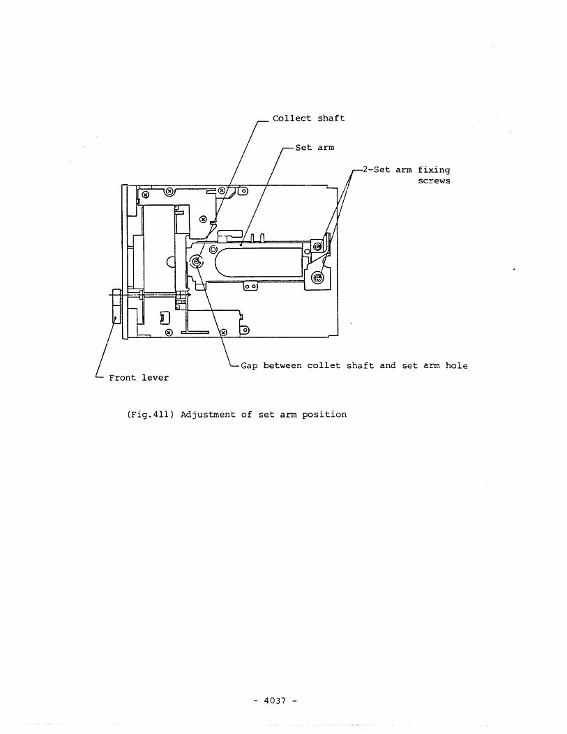
1Front lever
Collect shaft
arm fbcingsc~ews
Gap between collet shaft and set arm hole
(Fig.4l1) Adjustment of set arm position
- 4037 -
4-4-2. Check and Adjustment of Holder position
(A) Equipment
(1) Corss point screwdriver, M3
(2) ~X media jig C
(3) ~X media jig E
(B) Check and adjustment procedure
(1) Insert the ~X media jig E from open side until it strikes the frame
stopper. (See Fig.412).
(2) When closing the front lever at the stop side-of the MAX media jig E,
confirm that the wing of the front lever disturbs the rotation and that
the lever cannot be closed.
(3) When turning the MAX media jig E over to insert it for pass side, and
closing the front lever, confirm that the lever can be closed.
(4) If the item (2) or (3) is not satisfied, adjust the holder position
according to the following procedure.
(a) Loosen four fixing screws (see Fig.4l3) of the holder so that the
holder can be moved manually without going out of place.
(b) Install the MAX media jig C from open side to set it to be in contact
with the frame stopper.
(c) Turn the front lever to close position. Loosen the fixing screws of
the holder again to make the holder move toward the arrow indicated
direction in Fig.4l3; then depress the wing area of the front lever
against the MAX media jig C. Refer to Fig.414.
- 4038 -
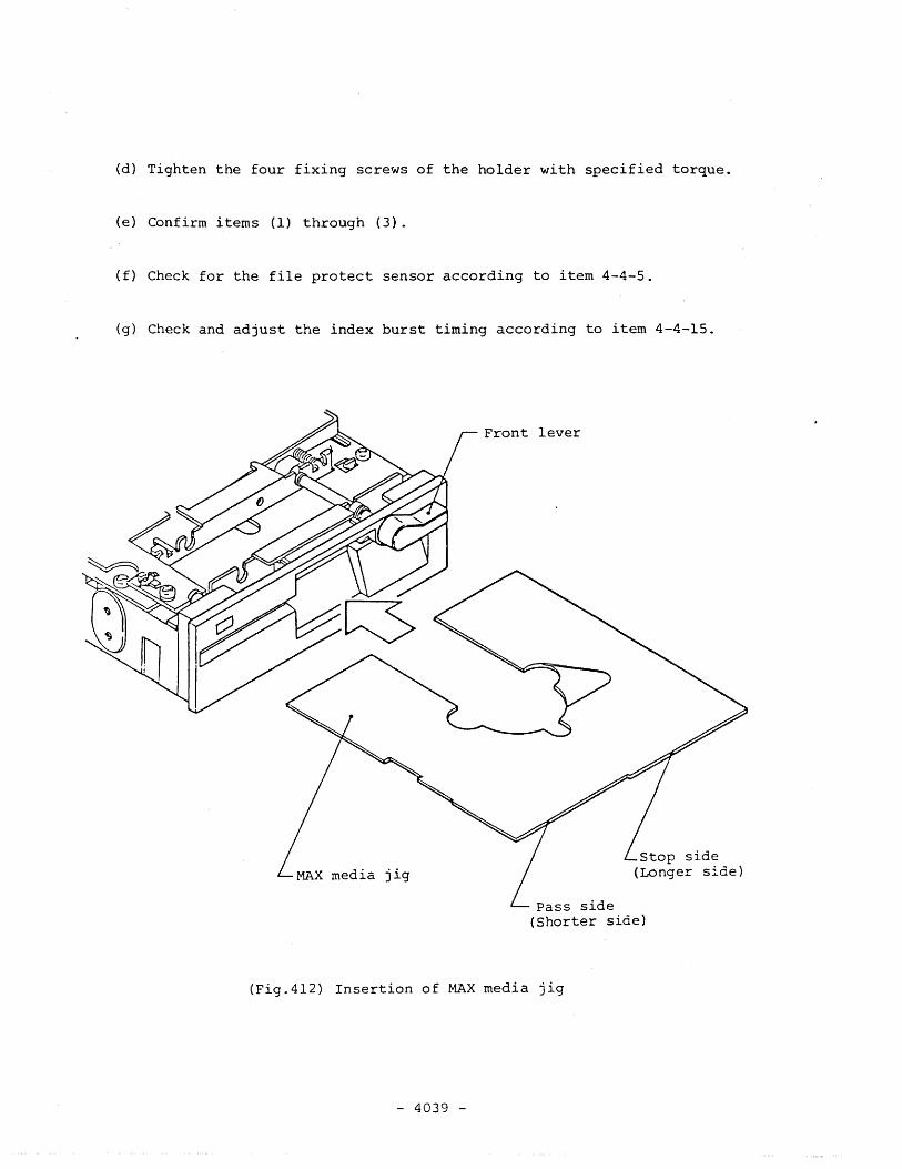
(d) Tighten the four fixing screws of the holder with specified torque.
(e) Confirm items (1) through (3).
(f) Check for the file protect sensor according to item 4-4-5.
(g) Check and adjust the index burst timing according to item 4-4-15.
jig
Front lever
Pass side(Shorter side)
(Fig.412) Insertion of MAX media jig
- 4039 -
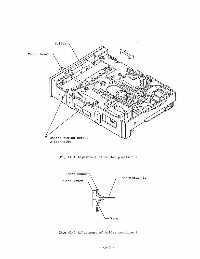
Front
Holder fixing screws2-each side
(Fig.413) Adjustment of holder position I
Front leverMAX media jig
(Fig.4l4) Adjustment of holder position 2
- 4040 -
4-4-3. Check and Adjustment of Arm Lifter
This item is applied only for the FDD with the head load solenoid, and
the .adjusting method is different for single sided and for double sided.
4-4-3-1. Double sided
(A) Equipment
(1) Common screwdriver, small size
(2) Work disk
(3) SKA or user's system
(4) Oscilloscope
(5) Locking paint
(B) Check and adjustment procedure
(1) General method
(a) Install a work disk and start the spindle motor.
(b) Set the head to track 00.
(c) Execute head loading.
(d) Confirm that the gap between the upper arm and the arm lifter is
larger than 0.2mm. If the gap is narrower than 0.2rnm, turn the
adjusting setscrew of the arm lifter. Refer to Figs.4l5 and 416.
(e) Unload the head.
(f) Confirm that the upper arm is lifted slightly by the arm lifter.
- 4041 -
Ann
Head carriage
lifting part
adjustingscrew
paint
Head loadsolenoid Ass'y
(Fig.4l5) Adjustment of arm lifter
Arm lifting part
O.2rnrn,Min.
Arm lifter
Note: Viewed from front bezel side.
(Fig.416) Gap of arm lifter
- 4042 -
Head carriage Ass'y
(g) Use two channels of oscilloscope. Connect the 1st channel to the
head load command signal and the 2nd channel to TP7 or TP8 on the
PCBA MFD control #H. Triggering is done by the head load command.
Oscilloscope range
The 1st channel: DC mode, 2V, 10msec
The 2nd channel: AC mode, 0.5 ~ IV, 10msec
Note: For the purpose of check and adjustment in this item, it is not
proper to execute the head loading by the MOTOR ON signal. Use
either of the DRIVE SELECT signal or the IN USE/HEAD LOAD signal.
Refer to item 4-2-4-8 or the Specification item 1-12-1).
(h) Select the side 1 head.
(i) Execute the head loading.
(j) Execute 2F write operation (WRITE DATA frequency of 250KHz for
FD-55AV ~ FV and 500KHz for FD-55GV) for one rotation of the disk.
(k) Unload the head.
(L) Repeat the head loading and unloading alternately (tapping operation)
and observe the waveform of TP7 or TP8 by the oscilloscope.
(m) Set the oscilloscope trigger to the positive mode and observe the read
waveform at TP7 or TP8 after the input of an unload command. Confirm
that there is no big spike noise (excludes a small one) or there is
not a continuous unload level (excludes the noise level) as shown
by dotted line in Fig.417.
In such event that either of the spike noise or continuous unload
level is observed in the waveform, fine adjust the setscrew of the
arm lifter.
- 4043 -
Head load command
Head load command
T1?7 or TP8
~ T_R_U_E _
..... -+__ Head load time(A/B~0.7 after 35ms)(Settled at sOrns)
Head unload command -1 FALSE
TP7 or TP8
"""'-'~~"'FFJ~FJ!""7"'rJ""JI~ .... , ~ Spike noise
----,---.--------- ----~~~~~~~~~:---1i---~----------
"-Residual read level(Unload level)
Head unload command
(Fig.4l7) Read waveforms at head loading/unloading
Note: This item shall be executed when the side 1 head is selected.
If the side 1 head is lifted too high during unload operation,
spike noise will be observed, while unload level will be observed
when it is too low.
(n) Set the oscilloscope trigger to the negative (-) mode and observe
the waveform at TP7 or TP8 after the input of a head load command.
Confirm that the read waveform more than SOrnsec after the head load
command is almost settled.
Or confirm that bottom "A" of the read level more than 3Smsec after
the input of the head load command is more than 0.7 against the
average read level "B". (A/B ~ O. 7 in Fig. 417) .
- 4044 -
(0) Make the head move to the innermost track.
(p) Repeat the procedure from item (i) to (n) and adjust so that the
items (m) and (n) are satisfied at track 00 and at the innermost
track.
(q) The items (m) and (n) are also applied to the side 0 head. However,
as to the unload level in item (m) will be excluded unless it is the
same read level as the head load condition.
Confirm in the same manner by selecting the side 0 head.
(r) Again set the head to track 00.
(s) After opening the front lever, draw out the disk slowly. In the
process of drawing out, the side 0 and side 1 heads shall not catch
the head window edge of the disk jacket (opening area of the jacket
to make the head be in contact with the disk ·surface). The jacket
can be drawn out smoothly with appropriate space margin.
(t) Insert the disk slowly and confirm that the disk jacket does not
touch the side 0 nor side 1 head and goes into the FDD smoothly with
appropriate space margin.
(u) If the items (p), (q), (s) or (t) is out of the specification,
following causes are assumed.
i) Inferior disk:
Disk and/or jacket is deformed or the disk may have drop-outs.
In such event, replace the work disk with a new one.
ii) Inferior head carriage ASs'y:
Replace the head carriage Ass'y according to item 4-5-1.
iii) Inferior head load solenoid:
Replace the head load solenoid Ass'y according to item 4-5-5.
iv} Inferior PCBA MFD control #H:
- 4045 -

Replace the PCBA MFD control #H according to item 4-5-7. (No
replation to items (5) and (t».
Note: Apply a drop of locking paint, if the setscrew is adjusted.
And if the strap setting is changed, back it to the initial setting
after th~ adjustment.
- 4046 -
(2) SKA method
(a) Connect the SKA according to item 4-2-4 and set the FD PWR switch
to the PSA side.
(b) Install a work disk.
(c) Start the spindle motor by key "5". {MON indicator turns on}.
(d) Execute drive select by key "0". COSO indicator turns on}.
(e) Key in "CO" and confirm that the TRACK indication becomes "00".
(RECALIBRATE)
(f) Confirm that the gap between the upper arm and the arm lifter is
larger than O.?mm. If the gap is narrower than 0.2mm, turn the
adjusting setscrew of the arm lifter. Refer to Figs.4l5 and 416.
(g) Release the drive select by key "0". (OSO indicator turns off).
(h) Confirm that the upper arm is lifted slightly by the arm lifter.
(i) Use two channels of oscilloscope. Connect the 1st channel to the
DOUT terminal and the 2nd channel to the OIF terminal of the SKA.
Apply negative trigger by the DOUT terminal.
Oscilloscope range
The 1st channel: DC mode, 2V, lOmsec
The 2nd channel: AC mode, 0.5 ~ IV, lOmsec
Note: For the check and adjustment in this item, it is required to set
the straps according to item 4-2-4-8.
- 4047 -
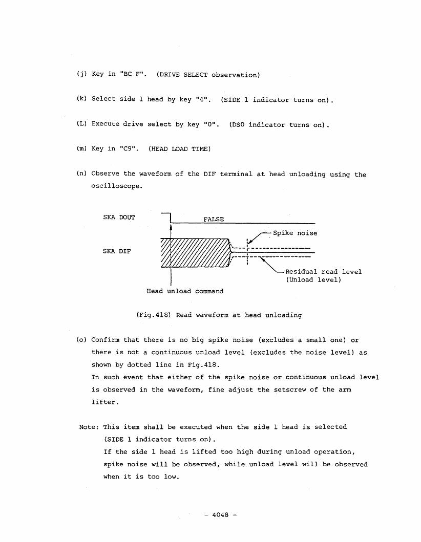
(j) Key in "BC F". (DRIVE SELECT observation)
(}<) Select side 1 head by key "4". (SIDE 1 indicator turns on) .
(L) Execute drive select by key "0". (050 indicator turns on) •
(m) Key in "C9". (HEAD LOAD TIME)
(n) Observe the waveform of the DIF terminal at head unloading using the
oscilloscope.
SKA DOUT
SKA DIF
IL... --.;;.F..;.,;A;.;;;.L...;,S...;;;E _
:~ Spike noise\ I---.----------------'---~--~.------------,. :
'-'-'f'-ol:....c...L..L...I.,..........c...J..,j........;J,I
Residual read level(Unload level)
Head unload command
(Fig.4IS) Read waveform at head unloading
(0) Confirm that there is no big spike noise (excludes a small one) or
there is not a continuous unload level (excludes the noise level) as
shown by dotted line in Fig.4lS.
In such event that either of the spike noise or continuous unload level
is observed in the waveform, fine adjust the setscrew of the arm
lifter.
Note: This item shall be executed when the side I head is ~elected
(SIDE 1 indicator turns on) .
If the side I head is lifted too high during unload operation,
spike noise will be observed, while unload level will be observed
when it is too low.
- 4048 -
(p) Confirm that the DATA indicator ~I~~~
value within the following range.
Head load settling level: 70%, Min.
{q} Key in "F". (STOP)
(%) of the SKA indicates a
(r) If the DSO indicator of the SKA is off, execute drive select by key
"0". (DSO indicator turns on).
(s) Key in "el". (SEEK TMAX) .
(t) Repeat the procedure from items (m) to (p) and adjust so that the
items (0) and (p) are satisfied at track 00 and at the innermost
track.
(u) Key in "F". (STOP)
(v) The items (0) and (p) are also applied to the side 0 head. However,
as to the unload level in item (0) will be excluded unless it is the
same read level as the head load condition.
Depress key "4" to turn off the SIDE 1 indicator of the SKA and
confirm in the same procedure of items (L) through Cu) for the side 0
head.
(w) Key in "CO" and confirm that the TRACK indication becomes "00".
(RECALIBRATE)
(X) After opening the front lever, draw out the disk slowly. In the
process of drawing out, the side 0 and side 1 heads shall not catch
the head window edge of the disk jacket (opening area of the jacket
to make the head be in contact with the disk surface). The jacket
can be drawn out smoothly with appropriate space margin.
(y) Insert the disk slowly and confirm that the disk jacket does not
- 4049 -

touch the side 0 nor the side 1 head and goes into the FDD smoothly
with appropriate space margin.
(z) If the items (t), (v), (x), or (y) is out of the specification, refer
to item (u) of "General method".
Note: Apply a drop of locking paint, if the setscrew is adjusted.
- 4050 -
4-4-3-2. Single sided
(A) Equipment
(1) Common screwdriver, small size
(2) Work disk
(3) SKA or user's system
(4) Locking paint
(B) Adjustment procedure
(1) General method
,(a) Install a work disk and start the spindle motor'.
(b) Set the head to track 00.
(c) Execute head loading.
(d) Cc~firm that the gap between the pad arm and the arm lifter is
larger than O.2rnrn. If the gap is narrower than 0.2rnrn, turn the
adjusting screw of the arm lifter. Refer to Figs.41S and 416.
(e) Unload the head.
(f) Confirm that the pad arm is lifted slightly by the arm lifter.
(g) Make the head move to the innermost track.
(h) Execute head loading and repeat the procedure from item (d) through (f).
(i) Set the head to track 00 again.
(j) Repeat the procedure of items (c) through (f).
- 4051 -

Note: After adjusting the setscrew, apply a drop of locking paint.
- 4052 -
(2) SKA method
(a) Connect the SKA according to item 4-2-4 and set the FO PWR switch
to the PSA side.
(b) Install a work disk.
(c) Start the spindle motor by key "5". (MON indicator turns on).
(d) Execute drive select by key "0". (050 indicator turns on).
(e) Key in "CO" and confirm that the TRACK indication becomes "00".
(RECALIBRATE)
(f) Confirm that the gap between the pad arm and the arm lifter is
larger than 0.2mm. If the gap is narrower than 0.2mm, turn the
adjusting setscrew of the arm lifter. Refer to Figs.4l5 and 416.
(g) Release the drive select by key "0". (050 indicator turns off).
(h) Confirm that the pad arm is lifted slightly by the arm lifter.
(i) Execute drive select by key "0". (050 indicator turns off) .
(j) Key in "Cl". (SEEKTMAX).
(k) Repeat the procedure of items (f) through (i).
(L) Key in "CO". (RECALIBRATE)
(m) Repeat the procedure of items (f) through (i).
Note: If the setscrew is adjusted, apply a drop of locking paint.
- 4053 -
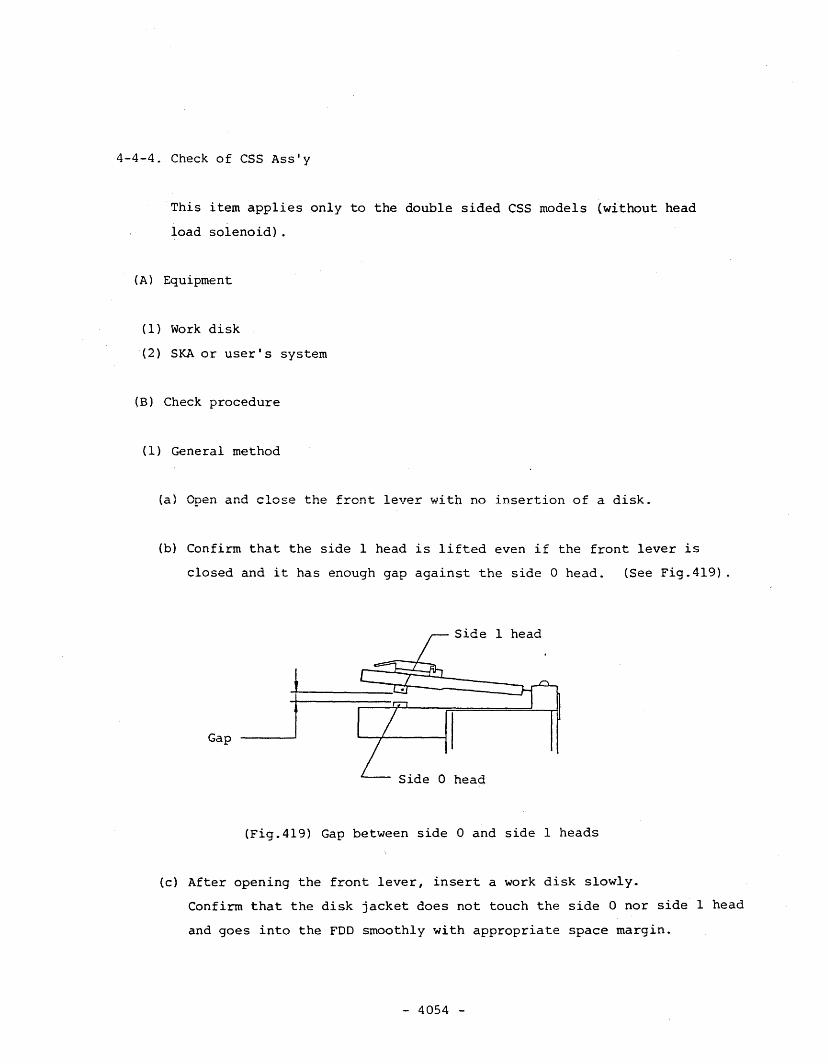
4-4-4. Check of CSS Ass'y
This item applies only to the double sided CSS models (without head
load solenoid) .
(A) Equipment
(1) Work disk
(2) SKA or user's system
(B) Check procedure
(l) General method
(a) Open the front lever with no insertion of a disk.
(b) Confirm that the side 1 head is lifted even if the front lever is
closed and it has enough gap against the side 0 head. (See Fig.4l9) .
Side 1 head
1Gap
o head
(Fig.4l9) Gap between side 0 and side 1 heads
(c) After opening the front lever, insert a work disk slowly.
Confirm that the disk jacket does not touch the side 0 nor side 1 head
and goes into the FDD smoothly with appropriate space margin.
- 4054 -
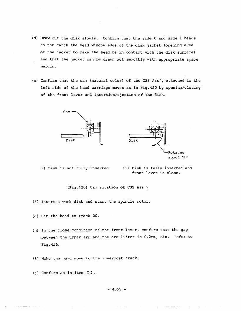
(d) Draw out the disk slowly. Confirm that the side 0 and side 1 heads
do not catch the head window edge of the disk jacket (opening area
of the jacket to make the head be in contact with the disk surface)
and that the jacket can be dra\m out smoothly with appropriate space
margin.
(e) Confirm that the cam (natural color) of the.CSS ASs'y attached to the
left side of the head carriage moves as in Fig.420 by opening/closing
of the front lever and insertion/ejection of the disk.
Cam
Rotatesabout 90°
i) Disk is not fully inserted. ii) Disk is fully inserted andfront lever is close.
(Fig.420) Cam rotation of CSS ASs'y
(f) Insert a work disk and start the spindle motor.
(g) Set the head to track 00.
(h) In the close condition of the front lever, confirm that the gap
between the upper arm and the arm lifter is 0.2mm, Min. Refer to
Fig.4l6.
(i) M.a'ke the hea.d move too the innermost t:t'3Ck:,
(j) Confirm as in item (h).
- 4055 -
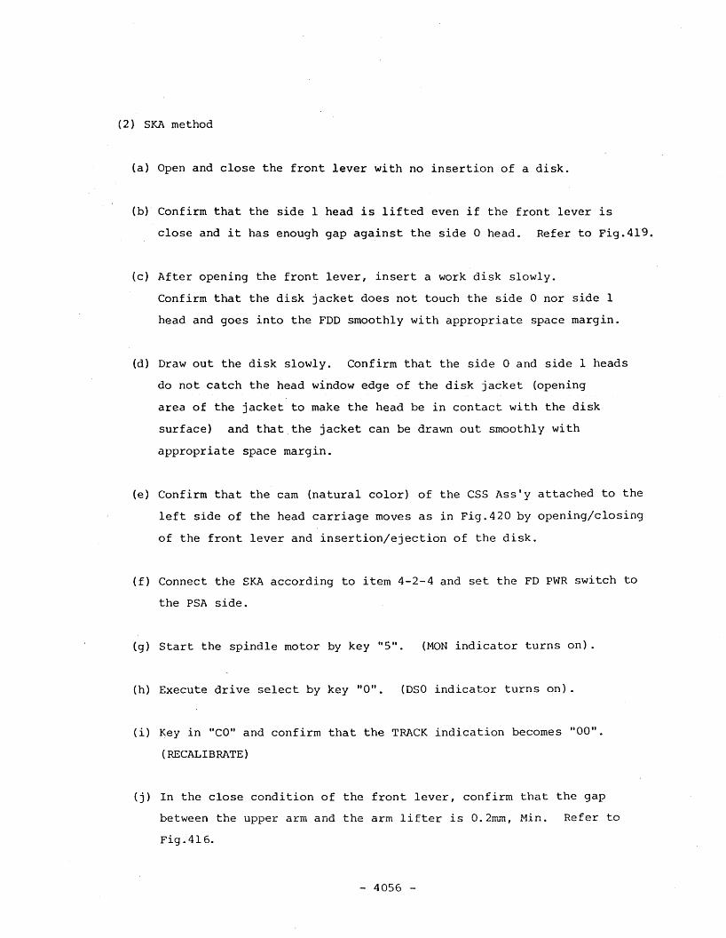
(2) SKA method
(a) Open and close the front lever with no insertion of a disk.
(b) Confirm that the side 1 head is lifted even if the front lever is
close and it has enough gap against the side 0 head. Refer to Fig.419.
(c) After opening the front lever, insert a work disk slowly.
Confirm that the disk jacket does not touch the side 0 nor side 1
head and goes into the FOO smoothly with appropriate space margin.
(d) Draw out the disk slowly. Confirm that the side 0 and side 1 heads
do not catch the head window edge of the disk jacket (opening
area of the jacket to make the head be in contact with the disk
surface) and that the jacket can be drawn out smoothly with
appropriate space margin.
(e) Confirm that the cam (natural color) of the CSS Ass'y attached to the
left side of the head carriage moves as in Fig.420 by opening/closing
of the front lever and insertion/ejection of the disk.
(f) Connect the SKA according to item 4-2-4 and set the FO PWR switch to
the PSA side.
(g) Start the spindle motor by key "5". (MaN indicator turns on) .
(h) Execute drive select by key "0". (050 indicator turns on).
(i) Key in "CO" and confirm that the TRACK indication becomes "00".
(RECALIBRATE)
(j) In the close condition of the front lever, confirm that the gap
between the upper arm and the arm lifter is 0.2rr~, Min. Refer to
Fig.4l6.
- 4056 -

(k) Key in "Cl". (SET TMAX) •
(L) Confirm as in item (j).
- 4057 -
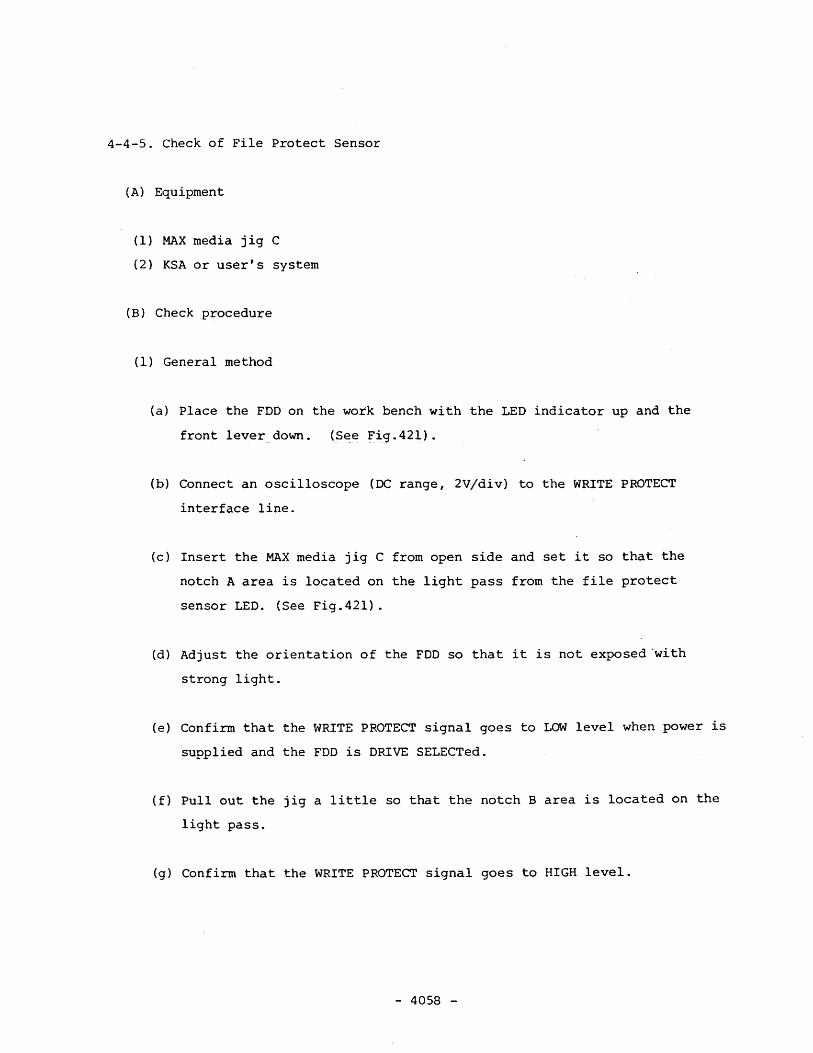
4-4-5. Check of File Protect Sensor
(A) Equipment
(1) MAX media jig C
(2) KSA or user's system
(B) Check procedure
(1) General method
(a) Place the FDD on the work bench with the LED indicator up and the
front lever down. (See Fig.42l).
(b) Connect an oscilloscope (DC range, 2Vjdiv) to the WRITE PROTECT
interface line.
(c) Insert the MAX media jig C from open side and set it so that the
notch A area is located on the light pass from the file protect
sensor LED. (See Fig.421).
(d) Adjust the orientation of the FDD so that it is not exposed ·with
strong light.
(e) Confirm that the WRITE PROTECT signal goes to LOW level when power is
supplied and the FDD is DRIVE SELECTed.
(f) Pullout the jig a little so that the notch B area is located on the
light pass.
(g) Confirm that the WRITE PROTECT signal goes to HIGH level.
- 4058 -
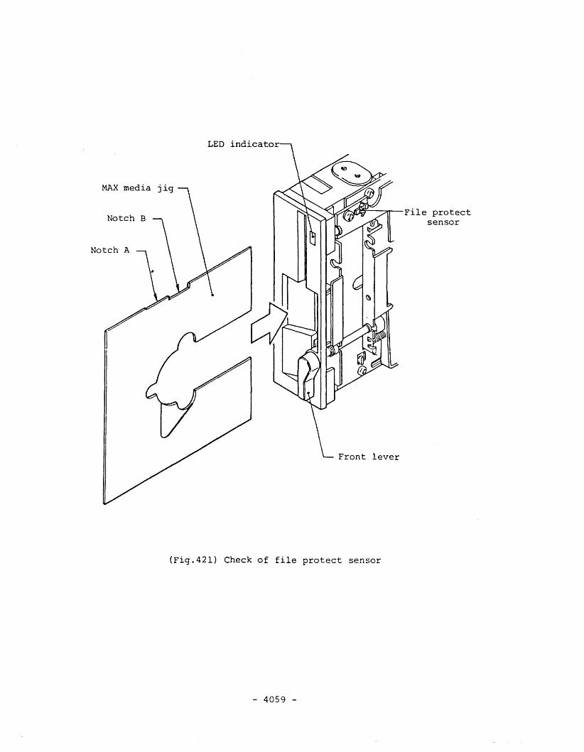
MAX media
Notch B
Notch A
Front lever
(Fig.42l) Check of file protect sensor
- 4059 -
File protectsensor

(2) SKA method
(a) Connect the SKA according to item 4-2-4 and set the FD PWR switch
to the PSA side.
(b) Insert the MAX media jig C from open side and set it so that the
notch A area is located on the light path from the file protect
sensor LED. (See Fig.42l).
(c) Adjust the orientation of the FDD so that it is not exposed with
strong light.
(d) Confirm that the WPROT indicator of the SKA turns on, when the FDD
is selected by key "0". (DSO indicator turns on).
(e) Pullout the jig a little so that the notch B area is located on the
light path.
(f) Confirm that the WPROT indicator turns off.
- 4060 -
4-4-6. Check of Disk Rotation Speed
Disk rotation speed is set to 300rpm for FD-55AV ~ FV and 360rpm for
FD-55Gv.
(A) Equipment
(1) SKA or user's system
(2) Frequency counter (not required when the SKA is used)
(3) Work disk (for high density)
(B) Check procedure
(1) General method
(a) Connect a frequency counter to TPl (Index) on the PCBA MFD control #H
or to the INDEX interface signal line.
(b) Install a work disk and start the spindle motor.
(c) Set the head to track 00.
(d) Execute the head loading.
(e) Confirm that the pulse interval at TPl or at the INDEX interface is
within the following range.
FD-55AV ~ FV: 200 ± 3rnsec
FD-55GV: 166.7 ± 2.5msec
- 4061 -
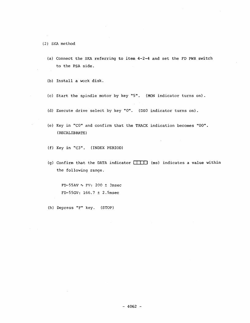
(2) SKA method
(a) Connect the SKA referring to item 4-2~4 and set the FD PWR switch
to the PSA side.
(b) Install a work disk.
(c) Start the spindle motor by key "5". (MON indicator turns on).
(d) Execute drive select by key l'O". (DSO indicator turns on).
(e) Key in "CO" and confirm that the TRACK indication becomes "00".
(RECALIBRATE)
(f) Key in "C3". (INDEX PERIOD)
(g) Confirm that the DATA indicator
the following range.
FD-55AV ~ FV: 200 ± 3msec
FD-55GV: 166.7 ± 2.5msec
(h) bepress "F" key. (STOP)
- 4062 -
(ms) indicates a value within
4-4-7. Check of Erase Gate Delay
The purpose of this item is to confirm the function of the control LSI.
This item is not so important as far as the FDD operates normally.
(A) Equipment
(1) SKA or user's system
(2) Oscilloscope (not required when the SKA is used)
(3) Work disk
(B) Check procedure
(1) General method
(a) Use two channels of oscilloscope. Connect the trigger channel to the
WRITE GATE interface line and the other channel to TP2 (Erase gate
delay) on the PCBA MFD control #H.
Oscilloscope range: For both channels, DC mode, 5V, 100~sec
(b) Install a work disk and start the spindle motor.
(c) Execute the head loading.
(d) Set the oscilloscope to the negative trigger (-) mode. Make the
WRITE GATE signal TRUE (write command).
(e) Confirm that "tl" (Erase on delay) in Fig.422 is within the following
range.
FD-55AV ~ FV: 200 ~ 320~sec
FD-55GV: 175 ~ 2l0~sec
(f) Set the oscilloscope to the positive trigger (+) mode. Make the
WRITE GATE signal FALSE.
- 4063 -
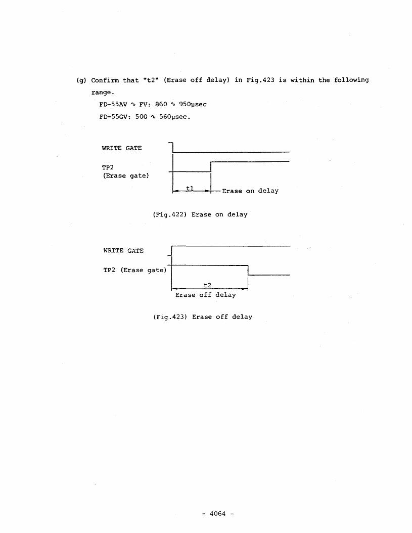
(g) Confirm that It2" (Erase off delay) in Fig.423 is within the following
range.
FO-55AV tV FV: 860 tV 95011sec
FO-55GV: 500 tV 56011sec.
WRITE GATE l _TP2(Erase gate)
..-..---::t::.=l=--_-+-- Erase on delay
(Fig.422) Erase on delay
~lRITE
TP2 (Erase
J
gate) -I. t2
Erase off delay.I
(Fig.423) Erase off delay
- 4064 -
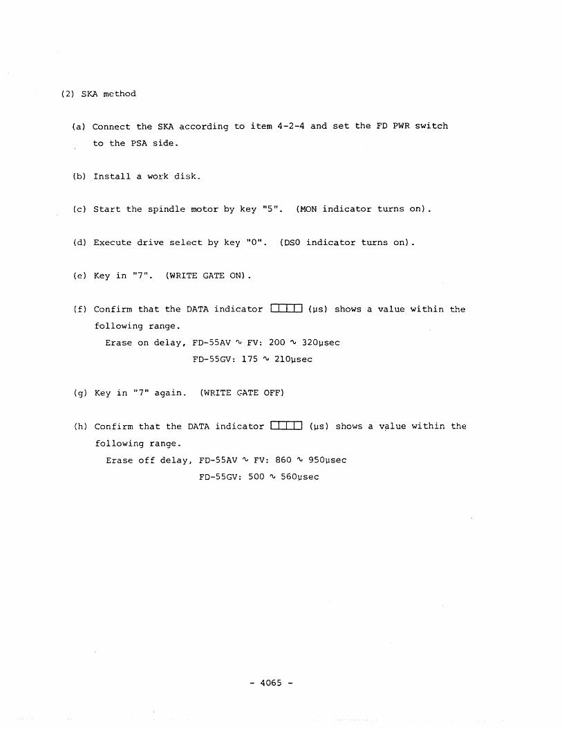
(2) SKA method
(a) Connect the SKA according to item 4-2-4 and set the FD PWR switch
to the PSA side.
(b) Install a work disk.
(c) Start the spindle motor by key "5". (MON indicator turns on).
(d) Execute drive select by key "0". (DSO indicator turns on).
(e) Key in "7". (WRITE GATE ON).
(f) Confirm that the DATA indicator (vs) shows a value within the
following range.
Erase on delay, FD-55AV ~ FV: 200 ~ 320~sec
FD-55GV: 175 ~ 210~sec
(g) Key in "7" again. (WRITE GATE OFF)
(h) Confirm that the DATA indicator (~s) shows a v~lue within the
following range.
Erase off delay, FD-55AV ~ FV: 860 ~ 950~sec
FD-55GV: 500 ~ 560~sec
- 4065 -
4-4-8. Check and Adjustment of Head Touch
Note: The adjustment is applied only to a single sided FDD.
tAl Equipment
(l) tvork disk
(2) Common screwdriver, small size
(3) SKA or user's system
(4) Oscilloscope (not required when the SKA is used)
(5) DC clip on ammeter (not required when the SKA is used)
(6) Locking paint
(B) Check and adjustment procedure
(1) General method
(a) Connect an oscilloscope to TP7 or TP8 (Differentiation amp.) on the
PCBA MFD control #H.
Oscilloscope range: AC mode, 0.1 ~ 0.2V
(b) Install a work disk and start the spindle motor.
(c) Set the head to the innermost track.
(d) Execute the head loading.
(e) Repeat the cycle of one write rotation and one read rotation.
Write data should be the fixed pattern of 2F (250KHz of WRITE DATA
frequency for FD-55AV ~ FV and 500KHz for FD-55GV) .
(f) Write down the average read level measured during the read operation
of item (e) .
- 4066 -
(g) Execute item (e) and (f) with a slight depression (very slight
depression easy to release: 10 ~ 20g) by a finger on the top of the
upper head (double sided) or of the pad arm (single sided), and
measure th~ ~verage read level as in item (f).
(h) Confirm that the read level measured in item (f) is greater than 80%
of that in item (g).
(i) For a double sided FOO, execute items (e) through (h) respectively
for side 0 and side 1 heads.
(j) After making the head move to track 00, execute items (e) through (i).
(k) Head touch adjustment for a single sided FOO:
i) At the innermost track, turn the groove on the upper side of the
head pad by 30° steps, approx. with a common screwdriver (see
Fig.424). At each turning of the groove, execute write and read
operations in item (e).
Be sure to take apart the. common screwdriver from the head pad
during write or read operation.
Note: Be careful not to push the head pad strongly with the common
screwdriver. Also do not touch the pad surface to which a
disk will be in contact.
ii) After turning the pad position around 360°, set the position again
to the position where the highest read level was obtained. Then
execute items (e) through (h) at the innermost track.
iii) Continue the operation until the item (h) is sufficiently
satisfied. Following causes are assumed for the insufficient
result in item (h) after fine adjustment of the pad position.
- 4067 -
CD Inferior head pad:
Replace the pad according to item 4-5-12.
Q) Inferior disk:
Disk and/or jacket is deformed or damaged. Replace the work
disk with a new one.
Q) Inferior pressure of the jacket pads:
If the jacket pad attached under the set arm (see Fig.505, Nos.4,
5, 6) does not touch the disk jacket surface, replace the pads.
Caution: If the jacket surface is excessively pressed, it might be
deformed or the spindle motor might be overloaded because
of increasing the rotation torque. If item CD is done,
measure the +12V current consumption of the FDD and confirm
that the current does not exceed 300mA by an DC clip-on
ammeter. For a commercially available general disks, the
desirable current is 250mA, Max.
@ Inferior head:
Replace the head carriage Ass'y according to item 4-5-1.
iv} Remove the work disk and apply a drop of locking paint around the
rotating area of the head pad. Be careful not to smear the groove
for common screwdriver with the locking paint.
(L) possible causes for the insufficient head touch in a double sided FDD:
Following causes are assumed for the insufficient result in items (h)
through (j) on a double sided FDD.
i) Inferior disk:
Disk and/or jacket is deformed or damaged. Replace the work disk
with a new one.
ii) Inferior head flexture:
Because of the failed performance of the arm lifter in item 4-4-3
(model with head load solenoid) or the failed performance of the
CSS Ass'y in item 4-4-4 (CSS model without head load solenoic),
- 4068 -
Head pad
Locking paint
o 0ead carriage
(Fig.424) Adjustment of head pad position (single sided FDD)
the flexture on which the head piece is located may be deformed.
Remove the disk. Then open and close the front lever slowly to
observe the gap between the side 1 and side 0 heads from the front
bezel. If the two head surfaces are not in parallel each other,
it is considered to be the deformation.
Replace the head carriage Ass'y according to item 4-5-1.
iii) Inferior pressure of the jacket pads:
If the jacket pad attached under the set arm (see Fig.SOS, No.4
and No.6) does not touch the jacket surface, replace the pads.
Caution: If the jacket surface is excessively pressed by the pad
No.6 (ronch pad): it might cause wear out of the disk or
the spindle motor might be overloaded because of increasing
the rotation torque.
- 4069 -
(2) SKA method
(a) Connect the SKA according to item 4-2-4 and set the FD PWRswitch
to the PSA side.
(b) Install a high density work disk.
(c) start the spindle motor by key "5". (MON indicator turns on).
(d) Execute drive select by key "0". (DSO indicator turns on).
(e) Key in "CO" and confirm that the TRACK indication becomes "00".
(RECALIBRATE)
(f) Key in "Cl". (SEEK TMAX)
(g) Key in "03". (WRITE/READ LEVEL PRE 2F)
(h) Write 2F and read operations are repeated.
The DATA indicator I I I I I (mV) indicates the average read level
of TP4 and TP5 (Pre-amp.)' after each cycle of operation (one rotation
of write and one rotation of read) is finished.
(i) Observe the DATA indicator I I I I I (mV) with a slight depression
(very slight depression easy to release: 10 ~ 20g) by a finger on
the top of the upper head.
(j) Confirm that the read level measured in item (h) is more than 80% of
that in item (i).
(k) For a double sided FOO, depress "F" key to stop and then depress "4"
key to execute items (g) through (j) for side 0 and side 1 heads
respectively. The side is changed alternately by a depression of
"4" key. If side 1 is selected, SIDE 1 indicator of the SKA turns Gn.
- 4070 -

(L) Key in "CO" (RECALIBRATE) and execute items (g) through (k) in the
similar way.
(rn) Head touch adjustment for a single sided POD:
Re fer to i tern (k) of "General method II •
+12V current consumption in item (k)-iii), "Caution" should be done
as follows.
i) Stop all the commands already input by depressing "p lI key.
ii} Key in "DP". (+12V CURRENT)
iii) Measure the +12V current consumption at that time by the DATA
indicator I I I I I (rnA).
iv} Key in "P" after the measurement completes. (STOP)
(n) Possible causes for the inferior head touch in a double sided POD:
Refer to item (L) of "General method".
- 4071 -
4-4-9. Check and Adjustment of Asymmetry
(A) Equipment
(1) Common screwdriver, small size
(2) Work disk (for high density)
(3) SKA or user's system
(4) Oscilloscope
(B) Check and adjustment procedure
(1) General method
(a) Connect an oscilloscope to the READ DATA interface line.
Oscilloscope range: DC mode, 2V, 0.5 ~ l~sec
(b) Install a work disk and start the spindle motor.
(c) Set the head to the innermost track.
(d) Execute the head loading.
(e) Execute IF write operation for one rotation of the disk (125KHz of
WRITE DATA frequency for FD-55AV ~ FV and 250KHz for FD-55GV).
(f) Measure the asymmetry referring to Fig.425.
Note: Oscilloscope should be so set that three READ DATA pulses can be
observed. Asymmetry width should be measured at the second READ
DATA pulse from the trigger pulse.
(g) Confirm that the aSYmmetry is within the following range.
Innermost track IF asymmetry, FD-55AV "" FV: 0.6~sec, Max.
FD-55Gv: 0.3~sec, Max.
- 4072 -
READ DATA
~ Asvrnmetrv
~--------~+-_. lF interval
Trigger
(Fig.425) Measurement of asymmetry
(h) For a double sided FDD, execute items (e) through (g) for side 0 and
side 1 heads respectively.
(i) If the value in item (g) or (h) is out of the specified range, adjust
according to the following procedure.
i) Adjust the variable resistor, Rl on the PCBA MFD control #H so
that the asymmetry takes a small value while repeating IF write
and IF read operations alternately.
ii) For a double sided FDD, repeat the operation in item i) for side 0
and side 1 heads alternately. The variable resistor shall be so
adjusted that both asymmetry for side 1 and side 0 heads take the
minimum value.
(j) If the adjustment in item (i) cannot be done sufficiently, or it is
too difficult to adjust, following causes are assumed.
i) Leakage flux density in the environmental condition of the FDD
is high:
If there is some flux source near the FDD such as magnet,
transformer, motor, Brown tube, magnetized iron plate, etc., take
it apart from the FDD. Then measure the asymmetry and adjust again.
ii) Inferior disk:
Replace the work disk.
iii) Inferior head:
Replace the head carriage Ass'y according to item 4-5-1.
- 4073 -

iv) Inferior PCBA MFD control #H:
Replace the PCBA according to item 4-5-7.
- 4074 -
(2) SKA method
(a) Connect the SKA according to item 4-2-4 and set the FD PWR switch
to the PSA side.
(b) Key in "BlF". (IF DUTY)
(c) Connect an oscilloscope to the DOUT terminal of the SKA.
Oscilloscope range: DC mode, 2V, 0.1 ~ 0.2~sec
(d) Install a work disk.
(e) Start the spindle motor by key "5". (MON indicator turns on).
(f) Execute drive select by key "0". (DSO indicator turns on).
(g) Key in "CO" and confirm that the TRACK indication becomes "00".
(RECALIBRATE)
(h) Key in "Cl". (SEEK TMAX)
(i) Key in "04". (WRITE/READ LEVEL PRE IF)
(j) Measure the asymmetry as in Fig.426#
Asynunetry
SKA DOUT J Cl__
U(Fig.426) Measurement of asymmetry
(k) Confirm that the asymmetry is within the following range.
- 4075 -
Innermost track IF asymmetry, FD-55AV '\" FV: O.6l-isec, Hax.
FO-55GV: 0.3l-isec, Max.
(L) For a double sided FOO, depress "4" key and execute items (i) through
(k) for side 0 and side 1 heads respectively. The side is changed
alternately by a depression of "4" key. If the side I is selected,
SIDE 1 indicator of the SKA turns on.
(m) If the value in item (k) or (L) is out of the specified range, adjust
according to the following procedure.
i) Adjust the variable resistor, Rl on the PCBA MFO control #H so
that the asymmetry takes a small value by keying in "04".
ii) For a double sided FOO, execute the oper~tion in item i) for
both sides alternately by changing the side by key "4". The
variable resistor shall be so adjusted that both asymmetry for
side 1 and side 0 heads take the minimum value.
(n) If the adjustment in item (m) cannot be done sufficiently, or if it
is too difficult to adjust, refer to item (j) of "General method".
- 4076 -
Measured value x 100/Calibration value(%)
4-4-10. Check of Read Level
(A) Equipment
(1) Level disk
(2) SKA or user's system
(3) Oscilloscope (not required when the SKA is used)
(B) Check procedure
(1) General method
(a) Use two channels of an oscilloscope and connect them to TP7 and TP8
(Differentiation amp.) on the PCBA MFD control .#H.
Oscilloscope range: AC mode, 0.2 ~ 0.5V
Set both channels, land 2 to the above range. Set either of the
channels to Invert mode and Add both channels.
(b) Install a level disk and start the spindle motor.
(c) Set the head to the innermost track.
(d) Execute the head loading.
(e) Execute 2F write operation for one rotation of the disk (250KHz of
WRITE DATA frequency for FD-55AV ~ FV and 500KHz for FD-55GV) .
(f) Measure the average amplitude (Vp-p) of the read waveform as in
Fig.427.
(g) Calculate the read level by substituting the following expression
with the measured value in item -Cf) and READ LEVEL calibration value
(see level disk label).
Read level (True value)
- 4077 -
TP 7, TP8 (Add)
..~ .0/~.::.
Vp-p
(Fig.427) Measurement of average read level (2F)
(h) Confirm that the true value of the read level- is O.8Vp-p, Min.
(i) For a double sided FDD,execute items (e) through (h) for side 0 and
side I heads respectively.
(j) If the value in item (h) or (i) is out of the specified range,
following causes are assumed.
i) Inferior disk:
Disk and/or jacket is deformed or cacaged. Replace the level disk
with a new one.
ii) Abnormal disk rotational speed:
Check for the speed according to ite~ 4-4-6.
iii} Inferior head touch:I
Check for the head touch according to item 4-4-8.
iv) Inferior head:
Replace the head carriage Ass'y according to item 4-5-1.
v) Inferior PCBA MFD control #H:
Replace the PCBA MFD control #H according to item 4-5-7.
(k) Eject the level disk and release the Invert and Add modes of the
oscilloscope.
- 4078 -
(2) SKA method
(a) Connect the SKA referring to item 4-2-4 and set the FO PWR switch
to the PSA side.
(b) Install a level disk.
(c) Start the spindle motor by key "5". (MON indicator turns on).
(d) Execute drive select by key "all. (DSO indicator turns on).
(e) Key in IICO II and confirm that the TRACK indication becomes 1100".
(RECALIBRATE)
(f) Key in IICI II . (SEEK TMAX)
(g) Key in "07". (WRITE/READ LEVEL DIF 2F)
Calibration value of the level disk should be set previously in the
SKA.
(h) Confirm that the DATA indicator
of 40OmVo-p, Min.
(mVo-p) indicates the value
(i) For a double sided FDO, depress key 114" and execute items (g) and
(h) for side a and side I heads respectively. The sid~ is changed
alternately by a depression of "4" key. If side 1 is selected, SIDE 1
indicator of the SKA turns on.
(j) If the value in item (h) or (i) is out of the specified range, refer
to item (j) of "General method".
(k) Eject the level disk.
- 4079 -
4-4-11. Check of Resolution
(A) Equipment
(1) Level disk
(2) SKA or user's system
(3) Oscilloscope (not required when the SKA is used)
(B) Check procedure
(1) General method
(a) Use two channels of an oscilloscope and connect them to TP4 and TP5
(Pre-amp.) on the PCBA MFD control #H.
Oscilloscope range: AC mode, 20mV " f"\ 1 't l'v V • ..LV
Set both channels, 1 and 2 to the above range. Set either of the
channels to Invert mode and Add both channels.
(b) Install a level disk and start the spindle motor.
(c) Set the head to the innermost track.
(d) Execute the head loading.
(e) Execute IF write operation for one rotation of the disA (125KHz of
WRITE DATA frequency for FD-55AV ~ FV and 250KHz for FD-55GV) .
(f) Measure the average amplitude (VIF) as in Fig.428.
(g) Execute 2F write operation as in item (e) (doubled in frequency to
that in item (e».
(h) Measure the average amplitude (V2F) as in Fig.428.
- 4080 -
TP4,TP5(Add) VIF
IF
(Fig.428) Measurement of resolution
2F
(i) Calculate the resolution by substituting the following expression
with the measured values VIF, V2F, and RESOLUTION calibration value
(see level disk label).
Resolution (true value) V2F/VIF x 100/Calibrat~on value (%)
(j) Confirm that the true value of resolution is within the following
range.
Innermost track resolution, FD-55AV, BV: 55%, Min.
FD-55EV, FV, GV: 60%, Min.
(k) For a double sided FDD, execute items (e) through (j) for side 0
and side I heads respectively.
(L) If the value in item (j) or (k) is out of the specified range,
following causes are assumed.
i) Inferior disk:
Disk and/or jacket is deformed or damaged. Replace the level
disk with a new one.
ii) Inferior disk rotational speed:
Check for the speed according to item 4-4-6.
iii) Inferior head touch:
Check for the head touch according to item 4-4-8.
iv) Inferior head:
- 4081 -

Replace the head carriage Ass'y according to item 4-5-1.
v) Inferior PCB~ MFD control #H:
Replace the PCBA MFD control #H according to item 4-5-7.
(m) Eject the level disk and release the Invert and Add modes of the
oscilloscope.
- 4082 -
(2) SKA method
(a) Connect the SKA referring to item 4-2-4 and set the FO PWR switch
to the PSA side.
(b) Install a level disk.
(c) Start the spindle motor by key "5". (MON indicator turns on).
(d) Execute drive select by key "0". (OSO indicator turns on).
(e) Key in "CO" and confirm that the TRACK indication becomes 1100 11•
(RECALIBRATE)
(f) Key in "CI". (SEEK TMAX)
(g) Key in "08". (RESOLUTION)
The calibration value of the level disk should be set previously in
the SKA.
(h) Confirm that the DATA indicator (\) indicates the value within
the following range.
Innermost track resolution, FO-55AV, BV: 55%, Min.
FO-55EV, FV, GFV: 60\, Min.
(i) For a double sided FOO, depress key "4" and execute items (g) and
(h) for side 0 head and side I head respectively. The side is
changed alternately by a depression of "4" key. If side 1 is
selected, SIDE 1 indicator of the SKA turns on.
(j) If the value in item (h) or (i) is out of the specified range, refer
to item CL) of "General method".
(k) Eject the level disk.
- 4083 -
4-4-12. Check and adjustment of Track Alignment
(A) Equipment
(1) Cross point screwdriver, M3
(2) Alignment disk
(3) Alignment adjustment jig or M3 screw of 15mm long
(4) SKA or user's system
(5) Oscilloscope
(6) Hygrometer
(7) Locking paint
(B) Check and adjustment procedure
Note: Check and adjustment of track alignment should be done in an
environment of general room temperature and humidity. Even if the
environmental condition is within the specified operational condition
extreemly high or low temperature, or extreemly high or low humidity
shall be avoided. Check and adjustment should be done after two
hours, Min. of storing in the above mentioned condition.
It is recommended that the orientation of the FDD for the track
alignment check is the same as when the FDD is actually installed
in the user's system.
(1) General method
(a) Use two channels of an oscilloscope and connect them to TP7 and TP8
(differentiation amp.) on the PCBA MFD control UIl. Also connect
the external trigger of the oscilloscope to TPl (Index) and apply
positive trigger.
Oscilloscope range: AC mode, 0.2 ~ O.SV, 20msec
Set both channels, 1 and 2 to the above range. Set either of the
channels to Invert mode and Add both channels.
- 4084 -
(b) Install an alignment disk and start the spindle motor.
(c) Execute the head loading.
(d) Set the head to the following alignment check track.
Alighment check track, 48tpi (FD-55AV, BV): Track 16
96tpi (FD-55EV, FV, GV): Track 32
(e) Confirm that two lobe patterns as in Fig.429 can be observed (it is
not necessary that the levels of VA and VB are equal).
TP7 and TP8 (Add)
48tpi
96tpi
(Fig.429) Alignment check lobe pattern
If only one lobe pattern can be observed or if two lobes become one
pattern, the head is not on the alignment check track.
In such event, execute step-out or step-in for the following tracks'
space to obtain the most similar waveform to that in Fig.429.
48tpi: 2 tracks
96tpi: 4 tracks
Note: The above number of tracks to be stepped is required to make the
alignment track position be fit with the magnetized condition of
the basic magnetized phase "A" of the stepping motor. If the
stepped track numbers are inassured, set it again from track 00
(TRACK 00 output signal becomes TRUE) .
- 4085 -
For a 48tpi FDD, the lobe pattern in Fig.429 shall be observed at
the even track, while it shall be observed at the track of
multiple number of four for a 96tpi FDD.
(f) After one or several step-outs from the check track, step in the head
to the check track again and measure VA and VB at that time,.
(g) Calculate the true value of misalignment by substituting the value
in item (f) and ALIGNMENT calibration value (see alignment disk label,
attention to the side).
VA-VBMisalignment{true value) = ( VA & VB x 100
Larger value in
- Calibration value) - (Relative humidity-50) x K
"K" is humidity compensation factor.
48tpi: K=0.26
96tpi: K=0.42
e.g. 96tpi, VA=0.58V, VB=O.6lV, Calibration value=-6{%)
Relative humidity= 65%:
Misalignment(true value)= {0.580~6~·6l x 100-{-6)} - (65-50)
x 0.42 ::: -5.2{%)
If the calculated value is positive, the magnetic head is shifted
inward from the reference position, while the head is shifted outward
from the reference position when the value is negative.
(h) Conversely, measure VA and VB when the head is on the alignment check
track by stepping-out after one or several step-ins.
(i) Calculate the true value of misalignment as described in item (g).
- 4086 -
(j) Confirm that both of the calculated values in items (a) and (i) are
within the following range.
True value of misalignment: 30%, Max.
(k) For a double sided FDD, execute items (d) through (j) for side a and
side 1 heads respectively.
(L) If the value in item (j) or (k) is out of the specified range, adjust
the track alignment according to the following procedure:
i) Loosen two fixing screws of the stepping motor a little.
ii) Insert the alignment adjustment jig or M3 screw from the back
side of the FDD as shown in Fig.430.
iii) Repeat step-in and step-out operations and adjust the misalignment
to be the smallest on the alignment check track during both
step-in and step-out operations by turning the jig or the screw
(stepping motor moves little by little) .
Note: When you adjust the alignment by observing the lobe pattern
using the oscilloscope, pay attention to the calibration value
on the alignment disk label and the ambient relative humidity.
(DCalibration value + (Relative humidity - 50) x K > 0:
When the left side lobe pattern level, VA is assumed as lilli,
lobe pattern ratio should be so adjusted that the right side
lobe pattern level VB takes the following value:
VB 1 -Calibration value + (Relative humidity - 50) x K
100
(DCalibration value + (Relative humidity - 50) x K ~ 0:
When the right side lobe patt,ern level; VB is assumed as 111 11
lobe pattern ratio should be so adjusted that the left side
lobe pattern level VB takes the following value.
- 4087 -
VA 1 -Calibration value + (Relative humidity - 50) x K
100
0.881 -VA
e.g. 96tpi, Calibration value = -6%, Relative humidity 35%:
-6 + (35 - 50) x 0.42 = -12.3 < 0
-6 + (35 - 50) x 0.42100
Therefore, the target value of VA when VB is assumed as 111 11
is 0.88.
iv) For a double sided FDD, repeat the adjusting operation in item
iii) alternately for side 0 and side,l heads until the both
misalignment take the smallest value.
v) Tighten the two fixing screws 6fthe stepping motor little by
little for adjusting the true value of misalignment after
tightening the screws with the specified torque to be within ±20%.
vi) Remove the alignment disk.
vii) Apply a drop of locking paint to the head of the stepping motor
fixing screws.
viii) Check and adjust the track 00 sensor according to item 4-4-13.
ix) Check or adjust the track 00 stopper according to item 4-4-14.
(m) Release the Invert and Add modes of the oscilloscope.
- 4088 -
Stepping motor
Alignment adjustment jig
(Fig.430) Adjustment of track alignment
- 4089 -
(2) SKA method
(a) Connect the SKA referring to item 4-2-4 and set the FD PWR switch to
the PSA side.
(b) Use two channels of an oscilloscope. Connect the 1st channel to the
DOUT terminal of the SKA and the 2nd channel to the DIP terminal
of the SKA. Apply positive trigger by OOUT terminal.
Oscilloscope range
The 1st channel: DC mode, 2V, 20msec
The 2nd channel: AC mode, 0.2 ~ O.SV, 20msec
(c) Key in "B9F". (INDEX observation)
(d) Install an alignment disk.
(e) Start the spindle motor by key "5". (MON indicator turns on) .
(f) Execute drive select by key "0". (DSO indicator turns on).
(g) Key in "CO" and confirm that the TRACK indication becomes "00".
(RECALIBRATE)
(h) Set the head to the alignment check track by the following operation:
48tpi (FD-SSAV,BV): Key in "C2 16" and confirm that the TRACK
indication becomes "16".
96tpi (FD-SSEV, FV, GV): Key in "C2 32" and confirm tha t the TRACK
indication becomes "32".
(i) Confirm that two lobe patterns as in Fig.429 can be observed by the
oscilloscope (it is not necessary that the levels of VA and VB are
equal) .
If only one lobe pattern can be observed or if two lobes become one
pattern, the head is not on the alignment check track.
- 4090 -
In such event, execute step-in or step-out of the following tracks'
space to obtain the most similar waveform to that in Fig.429. step
operation can be done by key "8" (STEP-IN) and key "9" (STEP-OUT). By
a depression of these keys, head will move for one track space.
48tpi: 2 tracks
96tpi: 4 tracks
Note: The above number of tracks to be stepped in required to make the
alignment track position be fit with the magnetized condition of
the basic magnetized phase "A" of the stepping motor.
For a 48tpi FDD, the lobe pattern shall be observed at the even
track, while it shall be observed at the track of multiple number
of four for a 96tpi FDD.
(j) For a 96tpi FDD, the following steps shall be done under the turn on
condition of the H GAIN indicator in order to improve the measurement
accuracy and switching of humidity coefficient. Turn on the B GAIN
indicator by depressing "DO" key.
For a 48tpi FDO, confirm the H GAIN indicator is off. If it is on,
turn it off by depressing "DO" key.
(k) Key in "E3". (ALIGNMENT)
Calibration value of the alignment disk and environmental relative
humidity should be set previously in the SKA.
(%) indicator are(L) Confirm all the indications on the DATA
within ±30%.
The initial digit of the DATA indicator is the symbol. ,L (+) mark
indicates that the head is shifted inward from the reference position,
while - mark indicates that the head is shifted outward.
{m} For a double sided FDD, execute the sa~c check fer side 1 ~cad acccrdi~g
to the following procedure.
- 4091 -
i) Key in 110 11 following the operation of item (L) (during execution
of £3 command) and confirm that SIDE 1 indicator turns on.
ii) Confirm as in item (L).
Note: In order to change the head to side 0, key in 110 11 again.
(SIDE I indicator turns off)~
(n) Depress IIF II key. (STOP)
(0) If the value in item (L) or (m) is out of the specified range, adjust
the track alignment according to the following procedure.
i) Loosen the two fixing screws of the stepping motor a little.
ii) Insert the alignment adjustment jig or M3 screw from the back
side of the FDD as shown in Fig.430.
iii) Key in IIE3 11 and adjust the jig or M3 screw so that the DATl\
indicator I I I I I (%) shows the smallest value. The stepping motor
moves little by little when the jig or the screw is turned.
iv) For a double sided FOO, repeat the adjusting operation in item iii)
alternately for side 0 and side I heads until the both misalignment
take the smallest value.
v) Tighten the two fixing screws of the stepping motor little by
little to obtain the value within ±20% on the DATA indicator when
the screws are tightened with the specified torque.
vi) Remove the alignment disk.
vii) Apply a drop of locking paint on the screw head of the stepping
motor fixing screws.
viii) Check and adjust the track 00 sensor according to item 4-4-13.
ix) Check or adjust the track 00 stopper according to item 4-4-14.
(p) Release the Invert and Add modes of the oscilloscope.
(q) If the H GAIN indicator of the SKA is on, key in 1100 11 again to turn
off the H GAIN indicator of the SKA.
- 4092 -
4-4-13. Check and Adjustment of Track 00 Sensor
(A) Equipment
(1) Cross point screwdrivers, M2.6, M3
(2) Work disk
(3) Alignment disk
(4) SKA or user's system
(5) Oscilloscope (or digital voltmeter)
(6) Locking paint
(B) Check and adjustment procedure
Note: Check and adjustment of the track 00 sensor using this general
method is not so precise. It is reco~~ended to use the SKA method
in item (2) as much as possible.
(1) General method
(a) Connect an oscilloscope or a digital voltmeter to TP3 (Track 00
sensor) on the PCBA MFD control #H.
Oscilloscope range: DC mode, lV
(b) Install a work disk and start the spindle motor.
(c) Execute the head loading
(d) Confirm that the voltage at TP3 is within the following range when the
head is set to track 00.
Track 00 position TP3 voltage: 3.7V, Min.
(e) Turn the power off of the FDD and then turn it on again. Confirm
that the stop position of the head carriage did not change at power
off and on. This item aims to confirm that the track 00 position
- 4093 -
matches the basic magnetized phase A of the stepping motor.
(f) Set the head to the following track.
48tpi (FD-55AV, BV): Track 02
"96tpi (FD-55EV, FV, GV): Track 04
(g) Confirm that the voltage at TP3 is within the following range at
the track position in item (f).
TP3 voltage at track 02 (48tpi) or 04 (96tpi): 0.5V, ¥BX.
(h) If the value in item (d), (e), or (g) is out of the specified range,
adjust the position of the track 00 sensor according to the following
procedure.
i) If the track 00 stopper (small metal ---_ ..... _,pd.L L.::> J is equipped, loosen
the fixing screw of the stopper (see Fig.433) and shift the
stopper in the step-out direction (make apart from the rear side
of the head carriage) .
Note: If the V-type carriage (refer to Table 505) is mounted, the
track 00 stopper is not equipped. Item i) is not required for
this case.
ii) Connect the oscilloscope to TP7 or TP8 (Differentiation amp.)
of the PCBA MFD control #H.
Oscilloscope range: AC mode, 0.2 ~ 0.5V, 20msec
iii) Install an alignment disk. The track alignment should be adjusted
correctly according to item 4-4-12.
iv) Make the head move to the position where the lobe pattern as in
Fig.429 can be observed.
v) Remove the alignment disk.
vi) Connect the oscilloscope or digital voltmeter to TP3 (Track 00
sensor) on the PCBA MFD control #H.
Oscilloscope range: DC mode, IV
vii) Step out the head for the following space from the position where
the normal lobe pattern is observed .
..;. 4094 -
48tpi: 15 tracks (the head will be on track 01)
96tpi: 30 tracks (the head will be on track 02)
viii) Install a work disk .
. ix) Loosen the fixing screw of the track 00 sensor (see Fig.431)
and move the sensor a little so that the voltage at TP3 falls
within the following range.
TP3 voltage at track 01 (48tpi) or track 02 (96tpi):
IV ~ 3V (2V, approx. center)
x) Confirm the items (d) through (g).
xi) Adjust the track 00 sensor position so that the values in items
(ix) and (x) satisfy the specification when the screw has been
tightened with the specified torque (3Kg.cm).
xii) If the track QO stopper is equipped, adjust the track 00 stopper
according to item 4-4-14.
carriage Ass'y
Track 00 sensor
00 sensorfixing screw
(Fig.431) Adjustment of track 00 sensor
- 4095 -
(2) SKA method
(a) Connect the SKA referring to item 4-2-4 and set the FD PWR switch to
the PSA side.
(b) Use two channels of socilloscope and connect them as follows:
i) The 1st channel: SKA OOUT terminal
DC mode, SV, S ~ 10msec
ii) The 2nd channel: PCBA MFD control #H TP3 (Track 00 sensor),
2V range
iii) External trigger: DIRECTION SELECT interface signal (Interface
connector pin N-o .18) or pin 3 of J3 (resistor
network PAl for terminator) on the PCBA MFD
control #H
(+) trigger.
(c) Key in "B8 F". (STEP observation)
(d) Install a work disk and start the spindle motor by key "SII.
(MaN indicator turns on) .
(e) Execute drive select by key "0". COSO indicator turns on).
(f) Set the step rate and the settling time as follows referring to item
4-2-4-3.
48tpi (FO-55AV, BV): Step rate 6msec, Settling time 15msec
96tpi (FD-55EV, FV, GV): Step rate 3msec, Settling time 15msec
(g) Key in "CO" and confirm that the TRACK indication becomes "00".
(RECALIBRATE)
(h) Key in IICS II . (TOO TIMING, SEEK ±5)
- 4096 -
(i) Measure the timing of points A and B and the voltages VL and VH
referring to Fig.432. The values should be with the following range.
TP3 clip timing, A: tA in Fig.432.
TP3 clip timing, B: tB in Fig.432.
TP3 voltage, VL: 0.5V, Max.
TP3 voltage, VH: 3.7V, Min.
Step-outDIRECTION SELECT(External trigger) J
1 2 3 4 5 1
Step-in
2 3 4 5SKA OOUT
TP3(Track 00 sensor)
-----r---
VH
--------OV
48tpi tAO"\Ams
Track 00
tB+3"--lms
detection
Track 00 detection
-t~---l-0'V4ms I
214 531 2SKA DOUT
TP3(Track 00 sensor)
Note: VL and VH shall be smooth without undulations
(Fig.432) Track 00 sensor output waveform
(j) Key in "F". (STOP)
- 4097 -
(k) Turn the FD PWR switch of the SKA off at the track 00 position and
then set it again to the PSA side. Confirm that the stop position
of the head carriage did not change at power off and on.
(L) If the value in item (i) or (k) .is out of the specified range, adjust
the position of the track 00 sensor according to the following
procedure.
i) If the track 00 stopper (small metal parts) is equipped, loosen
the fixing screw of the stopper (see Fig.433) and shift the stopper
in the step-out direction (make apartfrcm the rear side of the
head carriage).
Note: If the V-type carriage (refer to Table 505) is mounted, the
track 00 stopper is not equipped. Item i) is not required for
this case.
ii) Connect the 2nd channel of the oscilloscope to TP7 or TP8
(Differentiation amp.) of the PCBA ~~D control #H and change the
trigger to this channel.
Oscilloscope range: AC mode, 0.2 ~ 0.5V, 20msec
iii) Install an alignment disk. The track alignment should be correctly
adjusted according to item 4-4-12.
iv) Key in "COli and confirm that the track indicator becomes "00".
(RECALIBRATE) .
v) Key in the following number and confi~TI that two lobe patterns as
in Fig.429 can be observed.
48tpi: C2 16
96tpi: C2 32
If normal lobe pattern cannot be observed, move the head to the
track position where the typical lobe pattern can be observed by
stepping in by key "8" or by stepping out by key :'9".
vi) Remove the alignment disk.
vii) Key in the following number. (SET TRACK NUMBER)
48tpi: E4 16
96tpi: E4 32
- 4098 -
viii) Key in "C2 00". (SEEK 00)
Don I t key in "CO". (RECALIBRATE)
ix) Change the cor~ection of the oscilloscope as in item (b).
x) Key in "CS". (TOO TIMING SEEK ±S)
xi) Loosen the fixing screw of the track 00 sensor (see Fig.431) and
adjust the se~sor position where the requirements in item'(i) are
all satisfied.
xii) Repeat the adjustment so that the values in item (i) fall within
the specified range when the fixing screw has been tightened with
the specified torque (3Kg.cm).
xiii) If the track CO stopper is equipped, adjust the track 00 stopper
according to i~ern 4-4-14.
- 4099 -
4-4-14. Check and Adjustment of Track 00 Stopper
If V-type carriage (see Note 12 and Table 505 in item 5-2-1) is used,
adjustment of this item is not required.
(A) Equipment
(1) Cross point screwdriver, M3
(2) SKA or user's system
(B) Check and adjustment procedure
(1) General method
(a) Set the head to track 00.
(b) Step out the head from the track 00 position.
(c) Confirm that the head carriage does not move by the step-out command
(head carriage rests on track 00).
(d) Confirm that the gap between the head carriage and the extreme end
of the track 00 stopper is 0.1 ~ 0.45mm. (See Fig.433).
If the V-type carriage is mounted, the track 00 stopper (small metal
parts) is not equipped and the frame protruding point works like as
a stopper.
(e) Repeat step-in and step-out operations between track 00 and track 05.
Confirm that no impact sound can be heard betwep.n the head carriage
and the track 00 stopper.
(f) Turn off the FDD power and depress the head carriage lightly against
the track 00 stopper with fingers. (See Fig.433).
- 4100 -
(g) Confirm that the head carriage automatically returns to the initial
position (track 00) when the power is turned on again.
(h) If the small parts for track 00 stopper is equipped (for L-type
carriage, refer to Table 504), and if anyone of the items (d) through
(g) is not satisfied, adjust the track 00 stopper position according
to the following procedure.
i) Set the head to track 00.
ii) Loosen the fixing screw of the track 00 stopper. (See Fig.433).
iii) Adjust the stopper position so that t~e gap between the stopper
and the head carriage becomes 0.25mm, approx. And then tighten
the screw with the specified torque.
iv) Execute items (a) through (g).
- 4101 -
GaD0.1 tV 0.45nun
carriage Ass'y
(Track 00 stopper)
Stepping motor
fixingscrew)
Note: Track 00 stopper (small metal parts) is not equipped if theV-type carriage is mounted. For this case, frame protrudingpoint works like as a stopper.
(Fig.433) Check and adjustment of track 00 stopper
- 4102 -
(2) SKA method
(a) Connect the SKA referring to item 4-2-4 and set the FD PWR
switch to the PSA side.
(n) Execute drive select by key "0". (DSO indicator turns on).
(c) Key in "COli and confirm that the TRACK indication becomes "00".
(RECALIBRATE)
(d) Set the step rate and the settling time as follows referring to item
4-2-4-3.
48tpi (FD-SSAV, BV): Step rate 6msec, Settling time lSmsec
96tpi (FD-SSEV, FV, GV): Step rate 3msec, Settling time lSmsec
(e) Key in "9". (STEP OUT)
(f) Confirm that the head carriage does not move even if "9" is keyed in
(head carriage rests on track 00).
(g) Confirm that the gap between the head carriage and the extreme end
of the track 00 stopper is 0.1 ~ O.4Smm. (See Fig.433).
If the v-type carriage is mounted, the track 00 stopper (small metal
parts) is not equipped and the frame protruding points works like as
a stopper.
(h) Key in "CO" and key in "CS". (STEP TIMING, SEEK ±S)
(i) Confirm that no impact sound can be heard between the head carriage
and the track 00 stopper.
(j) Turn off the FD PWR switch of the SKA and depress the head carriage
lightly against the track 00 stopper. (See the arrow mark in Fig.433) .
- 4103 -

(k) Confirm that the head carriage automatically returns to the initial
position (track 00) when the FD PWR switch is set to the PSA side
again.
(L) If the small parts for track 00 stopper is equipped (for L-type
carriage, refer to Table 504), and if anyone of the items (g)
through (k) is not satisfied, adjust the track 00 stopper position
according to the following procedure.
i) Key in "CO" and confirm that the TRACK indication becomes "00".
(RECALIBRATE)
ii) Loosen the fixing screw of the track 00 stopper. (See Fig.433).
iii) Adjust the stopper position so that the gap between the stopper
and the head carriage becomes 0.25mm, approx.
And then tighten the screw with the specified torque.
iv) Execute items (a) through (k).
- 4104 -
4-4-15. Check and Adjustment of Index Burst Timing
(A) Equipment
(1) Cross point screwdriver, M3
(2) Alignment disk
(3) SKA or user's system
(4) Oscilloscope (not required when the SKA is used)
(B) Check and adjustment procedure
(1) General method
(a) Use two channels of an oscilloscope. Connect the 1st channel to TPl
(index) on the PCBA MFD control #H and the 2nd channel to TP4 or TP5
(Pre-amp.). Apply positive trigger by TP1.
Oscilloscope range
The 1st channel: DC mode~ 2V, 50~sec
The 2nd channel: AC mode, O.5V, 50~sec
(b) Install an alignment disk and start the spindle motor.
(c) Execute the head loading.
(d) Set the head to the following track:
48tpi (FD-55AV, BV): Track 01
96tpi (FD-55EV, FV, GV): Track 02
(e) Measure "t" in Fig.434.
(f) Substitute the following equation with the measured value in item
{e) and INDEX TIMTNG calibration value (see alignment disk label).
Index burst timing (true value) Measured value - Calibration value(~s)
- 4105 -
TPI (Index) J
TP4 or TPS
t Index burst dela
(Fig.434) Index burst timing
(g) Confirm that the true value of the index burst timing is within the
following range.
FD-SSAV ~ FV: 200 ± 200~sec
FD-SSGV: 165 ±165~sec
(h) If the value in item (g) is out of the specified range, adjust the
index sensor Ass'y position according to the following procedure.
i) Loosen the fixing screws (see Fig.43S) of the PCBA front OPT #H
and adjust its position to make the true value of the index burst
timing fall in the specified range in item (g).
ii) Repeat the adjustment so that the true value of the index burst
timing falls in the range of item (g) when the fixing screw has
been tightened with the specified torque (4.5Kg.cm).
(i) Remove the alignment disk.
- 4106 -
PCBA front OPT fixing screws
direction ofsensor
front OPT #H
Index sensor
(Fig.435) Adjustment of index sensor
- 4107 -
(2) SKA method
(a) Connect the SKA referring to item 4-2-4 and set the FD PWR switch to
. the PSA side.
(b) Install an alignment disk.
(c) Start the spindle motor by key "5". (MON indicator turns on).
(d) Execute drive select by key "0". (050 indicator turns on).
(e) Key in "CO" and confirm that the TRACK indication becomes "00".
(RECALIBRATE)
(f) Set the head to the index check track by the following operation:
48tpi (FD-55AV, BV): Key in "C2 01" and confirm that the TRACK
indication becomes "01".
96tpi (FD-55EV, FV, GV): Key in "C2 02" and confirm that the TRACK
indication becomes "02".
(g) Key in "E6". (INDEX TIMING)
The calibration value of the index timing should be set previously
in the SKA.
(h) Confirm that the DATA indicator
within the following range.
FD-55AV tV FV: 200 ± 200~sec
FD-55GV: 165 ± 165~sec
(i) Key in "F". (STOP)
(~s) indicates the value
{ . \\ J I If the value in item (h) is out of the specified range, adjust the
index sensor Ass'y position according to the following procedure
- 4108 -
i) Loosen the fixing screws (see Fig.435) of the PCBA front OPT #H
and its position so that the DATA indication under execution of
item (g) shows the median value in the specified range of item (h).
ii) Repeat the adjustment so that the DATA indication takes the median
value when the fixing screw has been tightened with the specified
torque (4.5Kg.cm)
iii) Depress "F" key. (STOP)
(k) Remove the alignment disk.
- 4109 -
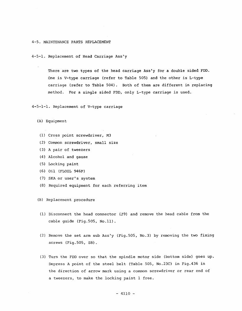
4-5. MAINTENANCE PARTS REPLACEMENT
4-5-1. Replacement of Head Carriage Ass'y
There are two types of the head carriage Ass'y for a double sided FDD.
One is v-type carriage (refer to Table 505) and the other is L-type
carriage (refer to Table 504). Both of them are different in replacing
method. For a single sided FDD, only L-type carriage is used.
4-5-1-1. Replacement of V-type carriage
(A) Equipment
(1) Cross point screwdriver, M3
(2) Common screwdriver, small size
(3) A pair of tweezers
(4) Alcohol and gauze
(5) Locking paint
(6) Oil (FLOIL 946P)
(7) SK~ or user's system
(8) Required equipment for each referring item
(B) Replacement procedure
(1) Disconnect the head connector (J9) and remove the head cable from the
cable guide (Fig.SOS, No.ll).
(2) Remove the set arm sub Ass'y (Fig. 505, No.3) by removing the two fixing
screws (Fig. 505, 58).
(3) Turn the FDD over so that the spindle motor side (bottom side) goes up.
Depress A point of the steel belt (Table 505, No.23C) in Fig.436 in
the direction of arrow mark using a common screwdriver or rear end of
a tweezers, to make the locking paint 1 free.
- 4110 -
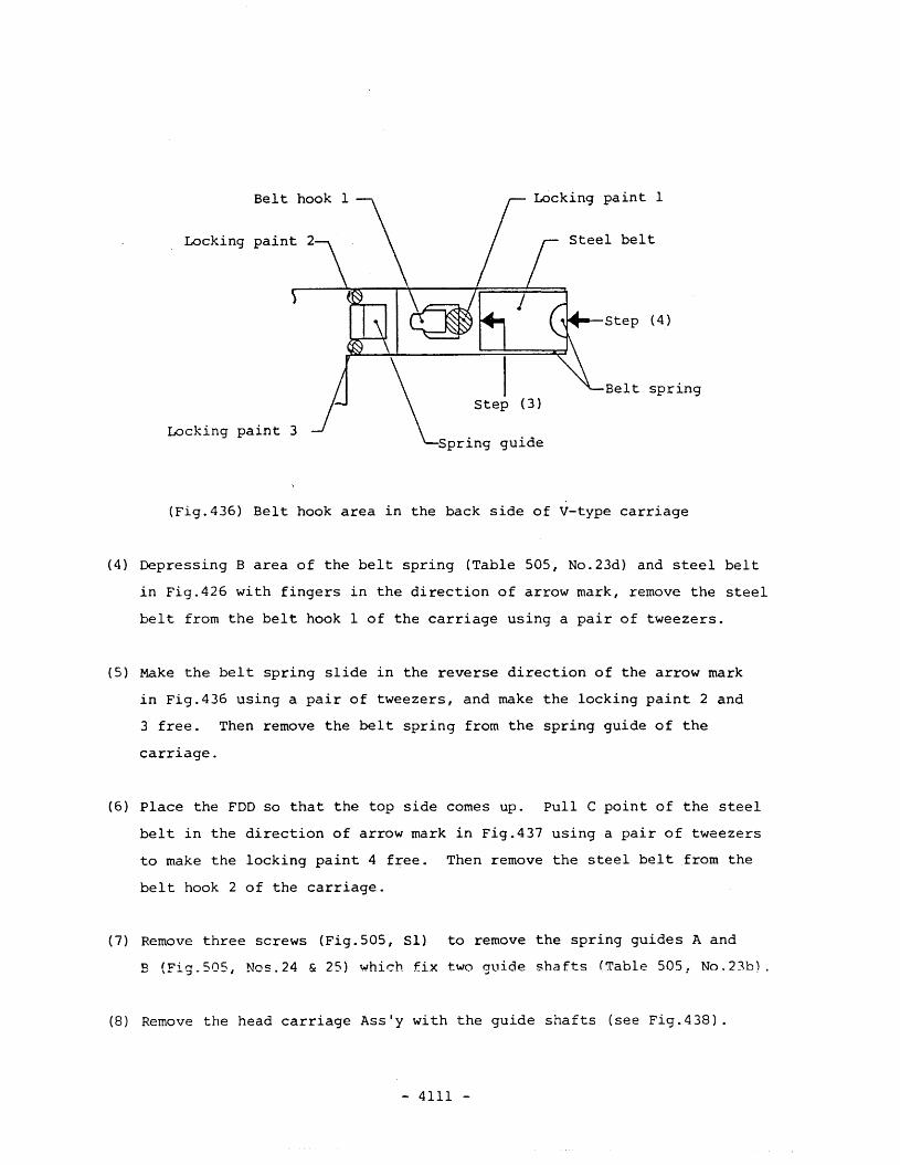
Belt hook
Locking
Locking paint 3
(3 )
guide
Steel belt
Step (4)
Belt spring
(Fig.436) Belt hook area in the back side of V-type carriage
(4) Depressing B area of the belt spring (Table 505, No.23d) and steel belt
in Fig.426 with fingers in the direction of arrow mark, remove the steel
belt from the belt hook 1 of the carriage using a pair of tweezers.
(5) Make the belt spring slide in the reverse direction of the arrow mark
in Fig.436 using a pair of tweezers, and make the locking paint 2 and
3 free. Then remove the belt spring from the spring guide of the
carriage.
(6) Place the FDD so that the top side comes up. Pull C point of the steel
belt in the direction of arrow mark in Fig.437 using a pair of tweezers
to make the locking paint 4 free. Then remove the steel belt from the
belt hook 2 of the carriage.
(7) Remove three screws (Fig. 505, Sl) to remove the spring guides A and
B (Fig. 505, Nos.24 & 25) which fix two guide shafts (Table 505 1 No.23b),
(8) Remove the head carriage Ass'y with the guide shafts (see Fig.438).
- 4111 -
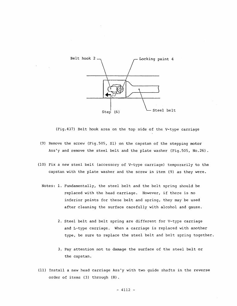
Belt hook 2
Step (6)
Locking paint 4
(Fig.437) Belt hook area on the top side of the V-type carriage
(9) Remove the screw (Fig.505, 51) on the capstan of the stepping motor
Ass'y and remove the steel belt and the plate washer (Fig. 505, No.26).
(10) Fix a new steel belt (accessory of V-type carriage) temporarily to the
capstan with the plate washer and the screw in item (9) as they were.
Notes: 1. Fundamentally, the steel belt and the belt spring should be
replaced with the head carriage. However, if there is no
inferior points for these belt and spring, they may be used
after cleaning the surface carefully with alcohol and gauze.
2. Steel belt and belt spring are different for V-type carriage
and L-type carriage. When a carriage is replaced with another
type, be sure to replace the steel belt and belt spring together.
3. Pay attention not to damage the surface of the steel belt or
the capstan.
(11) Install a new head carriage Ass'y with two guide shafts in the reverse
order of items (3) through (8).
- 4112 -
When fixing the steel belt to the carriage, install the belt spring
at the bottom side first, and hook the steel belt to the belt hook 1
(Fig.436) .
Then place the FDD with the top side up. Pull the steel belt in the
direction of arrow mark in Fig.437 using a pair of tweezers and hook
it to the belt hook 2.
Note: 4. When replacing the head carriage Ass'y, replace the two guide
shafts at the same time because of matching the respective hole
diameter of the carriage with those of the guide shafts. Each
guide shaft is to be designated in combination with corresponding
hole of the head carriage Ass'y.
Guide shaft ,which goes through the hole of the carriage smoothly
with a little clearance is considered to be the best.
(12) After finishing the installation of the carriage, loosen the screw
which fixes the steel belt to the capstan temporarily.
(13) Confirm that the steel belt runs on the center of the belt spring
in Fig.436.
(14) After moving the head carriage several times manually, tighten the
fixing screw of the steel belt in item (12) carefully with the
specified torque of 4.5Kg.cm. At this time, be careful that the belt
is tensioned straightly. Pay attention not to damage the surface of
the belt or the capstan.
Note: 5. Do not pinch the upper arm of the head carriage when move it
manually. Pinch the rear side of the carriage.
(15) Move the head carriage to the middle of movable area and apply a drop
of oil (FLOIL 946P) on three points of guide shafts' surface near the
shaft holes of the carriage. This item shall be omitted, if the oil
has been already applied.
- 4113 -
Notes: 6. A small drop of oil shall be applied to each point. For example,
dip the tip of a narrow object such as wire or a pair of
tweezers with oil.
7. If the head carriage or the head piece is smeared with oil, wipe
it out completely by such a cotton swab dipped with alcohol.
(16) Make the head carriage move manually several times to spread the oil
to allover the moving area.
(17) Referring Figs. 436 and 437, apply a drop of locking paint to four points
between the steel belt and the carriage (locking paint I through 4) .
(18) In the reverse order of items (1) and (2), install the set arm and
the head cable. Refer to item 4-2-3 as to the head cable treatment.
(19) Adjust the set arm position according to item 4-4-1.
(20) Model with head load solenoid:
Check and adjust the arm lifter according to item 4-4-3.
C55 model:
Check the C55 Ass'y according to item 4-4-4.
(21) Make the head move continuously between the track 00 and the innermost
track and confirm that the steel belt does not meander nor undulate.
When the 5KA is used, key in "C6" for this check and key in "F" for
stop.
Note: 8. If the steel belt is replaced with a new one, continue the head
seek operation in item (21) for 3 minutes, approx.
(22) Check the head touch according to item 4-4-8.
- 4114 -
(23) Adjust the asymmetry according to item 4-4-9.
(24) Adjust the track alignment according to item 4-4-12.
(25) Adjust the track 00 sensor position according to item 4-4-13.
(26) Check the track 00 stopper according to item 4-4-14.
(27) Check or adjust the index burst timing according to item 4-4-15.
(28) Check the read level according to item 4-4-10.
(29) Check the resolution according to item 4-4-11.
(30) If is recommended to connect the FDD to the system for overall test.
(Refer to items 4-2-5 (7) for window margin test).
- 4115 -
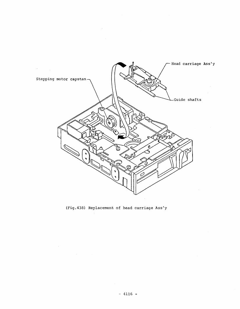
Stepping motor capstan
(Fig.438) Replacement of head carriage Ass'y
- 4116 -
carriage ASs'y
Guide shafts
4-5-1-2. Replacement of L-type carriage
(A) Equipment
(1) Cross point screwdriver, M3
(2) Common screwdriver, small size
(3) A pair of tweezers
(4) Alcohol and gauze
(5) Oil (FLOIL 946p)
(6) SK.~ or user's system
(/) Required equipment for each referring item
(B) Replace~ent procedure
(1) Disconnect the head connector (J9) and remove the head cable from the
cable guide CF ig .505, No. 11) •
(2) Remove the set arm sub ASs'y (Fig. 505, No.3) by removing the two fixing
screws (Fig. 505, 58).
(3) Remove two fixing screws connecting the head carriage (Table 504, No.22a)
and the steel belt A (Table 504, No.22c) and remove the steel belt and
the belt spring (Table 504, No.22d) from the carriage.
(4) Remove three screws (Fig.50S, 51) to remove the spring guides A and B
(Fig.50S, Nos.24 & 25) which fix two guide shafts (Fig.SOS, No.23d).
(5) Remove the head carriage Ass'y with the guide shafts (see Fig.438).
(6) Remove the screw (Fig. 505, 51) on the capstan of the stepping motor
Ass'y and remove the steel belt and the plate washer (Fig.SOS, No.26).
(7) Fix a new steel belt (accessory of L-type carriage) temporarily to the
caps~an with the plate washer and the screw in item (6) as they were.
- 4117 -
Notes: 1. Fundamentally, the steel belt and the belt spring should be
replaced with the head carriage. However, if there is no
inferior points for these belt and spring, they may be used
after cleaning the surface carefully with alcohol and gauze.
2. Steel belt and belt spring are different for v-type carriage and
L-type carriage. When a carriage is replaced with another type,
be sure to replace the steel belt and belt spring together.
3. Pay attention not to damage the surface of the steel belt or the
capstan.
(8) Install a new head carriage Ass'y with two guide shafts in the reverse
order of items (3) through (5). Two fixing screws of the steel belt
to the head carriage (refer to item (3» should be tightened with
looseness for temporarily fixing.
Note: 4. When replacing the head carriage Ass'y, replace the two guide
shafts at the same time because of matching the respective
hole diameter of the carriage with those of the guide shafts.
Each guide shaft is to be designated in combination with
corresponding hole of the head carriage Ass'y.
Guide shaft which goes through the hole of the carriage smoothly
with a little clearance is considered to be the best.
(9) After finishing the installation of the carriage, loosen the three
screws which fix the steel belt to the capstan temporarily.
(10) Confirm that the steel belt runs on the center of the belt spring
when viewed from the bottom side.
(11) After moving the head carriage several times manually, tighten the
fixing screw of the steel belt in item (9) carefully with the
specified torque of 4.5Kg.cm. At this time, be careful that the belt
- 4118 -
is tensioned straightly. Pay attention not to damage the surface of
the belt or the capstan.
Note: 5. Do not pinch the upper arm of the head carriage when move it
manually. Pinch the rear side of the carriage.
(12) Move the head carriage to the middle of movable area and apply a drop
of oil (FLOIL 946P) on three points of guide shafts' surface near the
shaft holes of the carriage. This item shall be omitted, of the oil
has been already applied.
Notes: 6. A small drop of oil shall be applied to each point. For example,
dip the tip of a narrow object such as wire or a pair of
tweezers with oil.
7. If the head carriage or the head piece is smeared with oil,
wipe it out completely by such a cotton swab dipped with alcohol.
(13) Make the head carriage move manually several times to spread the oil
to allover the moving area.
(14) In the reverse order of items (I) and (2), install the set arm and
the head cable. Refer to item 4-2-3 as to the head cable treatment.
(15) Adjust the set arm position according to item 4-4-1.
(16) Model with head load solenoid: Check and adjust the arm lifter
according to item 4-4-3.
C55 model: Check the C55 Ass'y according to item 4-4-4.
(17) Make the head move cont1nuously between the track 00 and the innermost
track and confirm that the steel belt does not meander nor undulate.
When the 5KA is used, key in "C6" for this check and key in "F" for
- 4119 -
stop.
If there is some abnor.mal running of the steel belt, readjust the
belt with three screws in item (9). After the adjustment tighten the
screws carefully with the specified torque of 4.5Kg.cm.
Note: 8. If the steel belt is replaced with a new one, execute the
continuous seek operation in item (17) for three minutes, approx.
(18) Check the head touch according to item 4-4-8.
(19) Adjust the asymmetry according to item 4-4-9.
(20) Adjust the track ~lignment according to item 4-4-12.
(21) Loosen the fixing screw (Table 504, SlO) of the track 00 stopper
(Table 504, No.22e) to shift the stopper toward the rear side of the
FDD.
(22) Adjust the track 00 sensor position according to item 4-4-13.
(23) Check the track 00 stopper according to item 4-4-14.
(24) Check or adjust the index burst timing according to item 4-4-15.
(25) Check the read level according to item 4-4-10.
(26) Check the resolution according to item 4-4-11.
(27) It is recommended to connect the FDD to the system for overall test.
(Refer to item 4-2-5 (7) for window margin test).
- 4120 -
4-5-2. Replacement of 5tepping Motor Ass'y
(A) Tools
(l) Cross point screwdriver, M3
(2) A pair of tweezers
(3) Alcohol and gauze
(4) Locking paint
(S) 5KA or user's system
(6) Required equipment for each referring item
(B) Replacement procedure
(1) Disconnect the stepping motor connector (J6).
(2) Remove the stepping motor cable form the cable hooks of the frame
(Pig. 505, No.1) to make the cable be free.
(3) Removal of steel belt and belt spring
(a) V-type carriage (refer to Table 505):
Remove the steel belt (Table 505, No.23c) and the belt spring (Table
505, No.23d) according to item 4-5-1-1 (3) through (6).
(b) L-type carriage (refer to Table 504):
Remove two screws (Table 504, 54) fixing the head carriage (Table 504,
No.22a) and the steel belt A (Table 504, No.22c), and remove the steel
belt and the belt spring (Table 504, No.22d) from the carriage.
(4) Remove the two fixing screws (Pig. 505, 59) of the stepping motor Ass'y
(Fig. 505, No.2?) and remove the stepping motor with the steel belt.
(5) Remove screw (Fig. 505, 51) on the capstan of the stepping motor and
remove the steel belt and the plate washer (Fig. 505, No.26).
- 4121 -
(6) Confirm that there is no inferior nor defective point for the steel
belt and belt spring. Then carefully clean the surface of the steel
belt, belt spring and capstan with alcohol and gauze.
If an inferior or defective point is found, replace the steel belt or
the belt spring with a new one.
(7) Fix the steel belt temporarily to the capstan of a new stepping motor
with the plate wa~herand the screw as they were.
Note: 2. Never remove the plate of the stepping motor Ass'y since they
are combined each other.
(8) Install the stepping motor in item (7) according to the reverse order
of items (1) through (4).
Note: 3. For a V-type carriage, install the belt spring at. the bottom side
first and hook the steel belt to the belt hook 1 (see Fig.436).
Then place the FDD with the top side up. Pull the belt in the
direction of arrow mark in Fig.437 using a pair of tweezers and
hook it to the belt hook 2.
For a L-type carriage, be careful to tension the steel belt
straightly and tighten the two screws temporarily.
(9) Loosen the screw which fixes the steel belt to the capstan.
If the L-type carriage is mounted, loosen another two screws which fix
the steel belt to the carriage.
(10) Confirm that the steel belt runs on the center of the belt spring when
- 4122 -
viewed from the bottom side.
(11) After moving the head carriage several times manually, tighten the
fixing screw of the steel belt in item (9) carefully with the specified
torque of 4.5Kg.cm. At this time, be careful so that the belt is
tensioned straightly. Pay attention not to damage the surface of the
belt or the capstan.
Note: 4. Do not pinch the upper arm of the head carriage when move it
manually. Pinch the rear side of the carriage.
(12) Make the head move continuously between the track 00 and the innermost
track and confirm,that the steel belt does not meander nor undulate.
When the SKA is used, key in lC6" for this check and key in "F" for
stop. If there is some abnormal running of the steel belt, readjust
the belt with screws in item (9). After the adjustment tighten the
screws carefully with the specified torque of 4.5Kg.cm.
Note: 5. If the steel belt is replaced, execute the continuous seek
operation in item (12) for three minutes, approx.
(13) Adjust the track alignment according to item 4-4-12.
(14) This item is applied only for the L-type carriage:
Loosen the fixing screw (Table 504, SlO) of the track 00 stopper
(Table 504, No.22e) to shift the stopper toward the rear side of the
FDD.
(15) Adjust the track 00 sensor position according to item 4-4-13.
(16) Check the track 00 stopper according to item 4-4-14.
- 4123 -
4-5-3. Replacement of DO motor Ass'y (Spindle Motor)
CA) Tools
(1) Cross point screwdriver, M3
(2) Common screwdriver, small size
(3) A pair of tweezers
(4) Locking paint
(5) SKA or user's system
(6) Required equipment for each referring item
(B) Replacement procedure
(1) Disconnect the spindle motor connector (J7).
(2) Remove three screws (Fig. 505, SS) of the DO motor Ass'y from the upper
side of the FDD and draw out the DO motor Ass'y from the rotor side
(PCBA side).
(3) Install a new DO motor Ass'y in the reverse order.
Note: The spindle area of the DO motor (clamping cup of the disk) is
precisely machined. For installing the motor to the frame,
place the spindle in parallel to the frame and push into the frame
slowly. Handle the spindle very carefully not to damage the spindle
surface.
(4) Arrange the DD motor cable according to Fig.439.
If the cable hook of the frame is the left type in Fig.439 (hook A),
cable shall be formed so that it is threaded cutside of the hook A.
Do not thread the cable through the hook which might cause cable be
in contact with the disk.
If the cable hook is the right type in Fig.439 (hook B), thread the
cable through the hook B normally.
- 4124 -
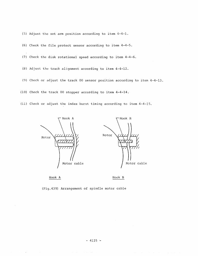
Motor cable
(5) Adjust the set arm position according to item 4-4-1.
(6) Check the file protect sensor according to item 4-4-5.
(7) Check the disk rotational speed according to item 4-4-6.
(8) Adjust the track alignment according to item 4-4-12.
(9) Check or adjust the track 00 sensor position according to item 4-4-13.
(10) Check the track 00 stopper according to item 4-4-14.
(11) Check or adjust the index burst timing according to item 4-4-15.
Hook A Hook B
(Fig.439) Arrangement of spindle motor cable
- 4125 -
4-5-4. Replacement of Collet Ass'y
(A) Equipment
(1) Cross point screwdriver, M3
(2) A pair of tweezers
(3) Round nose pliers
(4) Locking paint
(5) 5KA or user's system
(6) Required equipment for each referring item
(B) Replacement procedure
(1) Remove the set arm (Fig. 505, No.3) by removing the two fixing screws
(Fig.505, 58).
(2) Remove the E-ring (Fig. 505, 512) which fixes the collet Ass'y (Fig.SOS,
No.9) to the set arm and remove the collet and the pressure spring
(Pig.S05, No.IO).
(3) Install a new collet Ass'y in the reverse order. Pay attention to the
orientation of the spring. The spring is conical. The smaller
diameter side faces the collet side and the larger diameter side faces
the set arm side.
(4) Adjust the set arm position according to item 4-4-1.
(5) Check (or adjust) the track alignment according to item 4-4-12.
- 4126 -
4-5-5. Replacement of Head Load Solenoid
This item applies only for the FDD with the head load solenoid.
(A) Tools
(1) Cross point screwdriver, M3
(2) Hexagon wrench key, 1.5mm
(3) A pair of tweezers
(4) Locking paint
(5) SKA or user's system
(6) Required equipment to each referring item
(B) Replacement procedure
(1) Disconnect the head load solenoid and the track 00 connector (J4).
(2) Pullout two solenoid pins (terminal Nos. land 2) from the connector
housing referring to item 4-2-2, (4).
(3) Remove two fixing screws (Fig. 505, S2) to remove the head load solenoid
Ass'y (Fig.505, No.20).
(4) Install a new head load solenoid Ass'y in the reverse order.
Note: Arrange the wiring connection of the head load solenoid so that the
white lead wire is connected to pin 1 and the red wire to pin 2.
Refer to Fig.440.
(5) position the head load solenoid Ass'y so that the rod of ~2mm be in
parallel with the set arm. Refer to Fig.44l.
The space between the head protector ASs'y and the arm lifter shall be
more than 0.2mm. Then tighten the screws with the specified torque.
- 4127 -
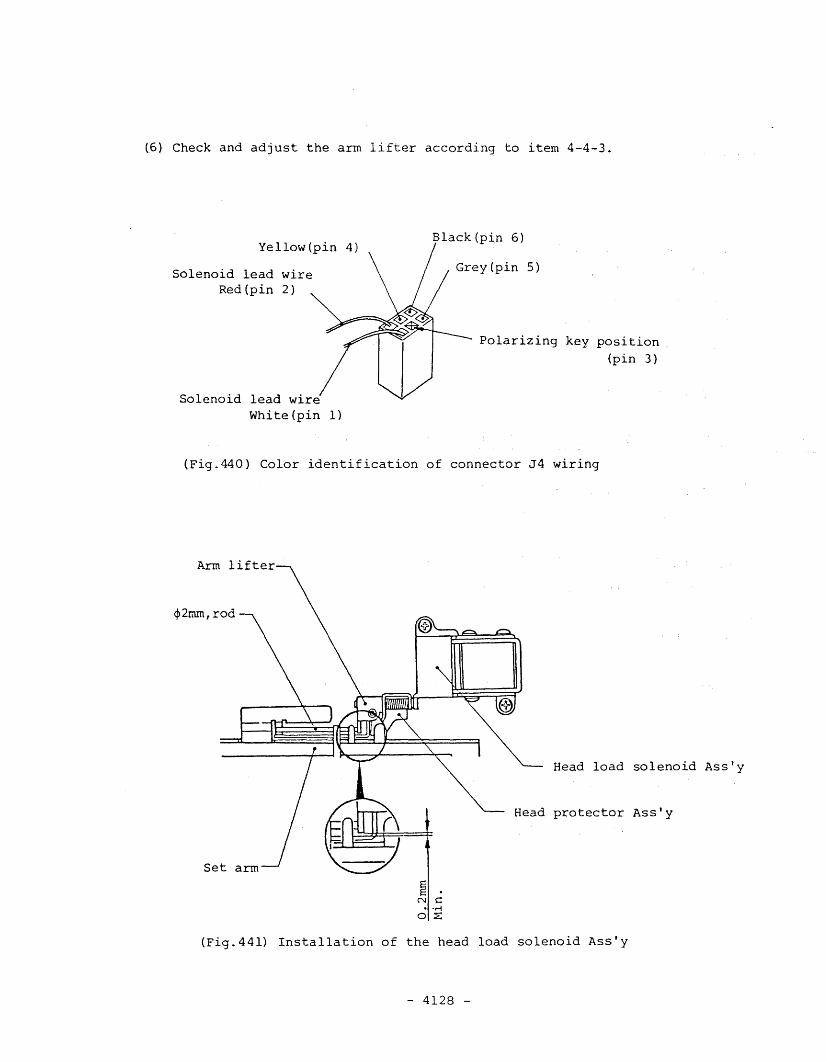
(6) Check and adjust the arm lifter according to item 4-4-3.
Yellow(pin 4)
Solenoid lead wireRed(pin 2)
Solenoid lead wireWhite(pin 1)
Black(pin 6)
Grey(pin 5)
Polarizing key position
(pin 3)
(Fig.440) Color identification of connector J4 wiring
Arm lifter
Head load solenoid Ass'y
Head protector Ass'y
~ .C'\I C
• -..-io:::E;
(Fig.44l) Installation of the head load solenoid Ass'y
- 4128 -
4-5-6. Replacement of PCBA Track 00 Sensor #H
(A) Tools
(1) Cross point screwdriver, M3
(2) A pair of tweezers
(3) Locking paint
(4) 5KA or user's system
(5) Required equipment for each referring item
(B) Replacement procedure
(1) Disconnect the head load solenoid and the Track 00 connector (J4).
(2) Pullout two solenoid pins (terminal Nos.l and 2) from the connector
housin9 referring to item 4-2-2, (4).
(3) Remove the fixing screw (Fig. 505, 56) to remove the PCBA TOO sensor #H
(Fig.50S, No.19).
(4) Install a new PCBA TOO sensor in the reverse order.
Note: Araange the wiring connection of the head load solenoid so that the
white lead wire is connected to pin 1 and red wire to pin 2. (See
Fig.440).
(S) Adjust the track 00 sensor position according to item 4-4-12.
(6) Check the track 00 stopper according to item 4-4-13.
- 4129 -
4-5-7. Replacement of PCBA MFD Control #H
(A) Tools
(1) Cross point screwdriver, M3
(2) Cornmon screwdriver, small size
(3) SKA or user's system
(4) Required equipment for each referring item
(B) Replacement procedure
(1) Disconnect all of the connectors connected to the PCBA MFD control #H
(Fig. 505, No.29) referring to item 4-2-2.
(2) Remove the PCBA by removing the three fixing screws (Fig. 505, 53).
(3) Install a new PCBA in the reverse order.
(4) Set the straps and terminator as they were on the old PCBA.
(5) Check the file protect sensor according to item 4-4-5.
(6) Check the erase gate delay according to item 4-4-7.
(7) Adjust the asymmetry according to item 4-4-9.
(8) Check the read level according to item 4-4-10.
(9) Check the resolution according to item 4-4-11.
(10) Check the track 00 sensor according to item 4-4-13.
(11) Check the index burst timing according to item 4-4-15.
- 4130 -

(12) It is recommended to connect the FDD to the system for overall test.
(Refer to items 4-2-5 (7) for window margin test).
- 4131 -
4-5-8. Replacement of PCBA Front OPT #H
(A) Tools
(1) Cross point screwdriver, M3
(2) SKA or user's system
(3) Required equipment for each referring item
(B) Replacement procedure
(1) Disconnect PCBA front OPT #H connector (J5J.
(2) Remove the two fixing screws (Fig.505, 57) to remove the PCBA.
(3) Install a new PCBA in the reverse order.
(4) Check the file protect sensor according to item 4-4-5.
(5) Adjust the index burst timing according to item 4-4-15.
(6) Check the performance.of the front bezel indicator.
- 4132 -
4-5-9. Replacement of Front Bezel Ass'y
(A) Tools
(1) Cross point screwdriver, M3
(2) Required equipment for each referring item
(B) Replacement procedure
(l) Draw out the front lever Ass'y (Fig.SOS, No.32).
(2) Remove the fixing screws (Fig. 505, S8) of the front bezel Ass'y (Fig. 505,
No.3l) and draw the front bezel out.
(3) Install a new front bezel Ass'y in the reverse order. For the
installation of the front bezel, press the longitudinal ends of the
bezel against the frame and tighten the fixing screws with the
specified torque.
(4) Insert the front lever Ass'y fully against the lever shaft as it was.
- 4133 -
4-5-10. Replacement of Front Lever Ass'y
(A) Tools
(1) Required equipment for each referring item
(B) Replacement procedure
(l) Draw out the front lever ASs'y (Fig.SOS, No.32).
(2) Insert a new front lever Ass'y fully against the lever shaft as it was.
(3) Check (or adjust) the holder position according to item 4-4-2.
- 4134 -
4-5-11. Replacement of CSS Ass'y
This item applies only to the CSS model (without head load solenoid).
(A) Tools
(1) Cross point screwdriver, M3
(2) Required equipment for each referring item
(B) Replacement procedure
(1) Remove the fixing screw (Fig.50S, S2) to remove the CSS Ass'y (Fig. 505,
No.2l) from the frame.
(2) Install a new CSS Ass'y in the reverse order. Be careful to install
the arm lifter area (~2mm rod) to be in pa~allel to the set arm.
The CSS Ass'y shall be fixed with no contact to the set arm. (Refer
to Fig.442).
(3) Check the CSS Ass'y according to item 4-4-4.
~2mm,rod
(Parallel to set arm)
Set arm
(Fig.442) CSS Ass'y and shift lever position
- 4135 -
4-5-12. Replacement of Head Pad (single sided)
This item applies only to the single sided FDD.
(A) Equipment
(1) A pair of tweezers
(2) Required equipment for each referring item
(B) Replacement procedure
(1) Lift up the pad arm manually and peel the pad carefully with a pair
of tweezers. (Se~ Fiq.443) .
(2) Apply a new pad to the original position. Do not press the pad
surface strongly.
(3) Check or clean the magnetic head surface according to item 4-3-2.
(4) Adjust the head pad position according to item 4-4-8.
(5) Check the read level according to item 4-4-10.
(6) Check the resolution according to item 4-4-11.
- 4136 -
PadPad arm
Head carriage Ass'y
(single sided)
(Fig.443) Replacement of head pad
- 4137 -
-
r'-tt • ..
-,--)<
-'.--------)<
-'-----~
)(
~-
-,,-----,..",,-
-----x~,
----"")(
f--
---_.-)(
f--
552 A I ' 1" 3 ••D-8llM
1~1"11 irJd991 IfUi'A, I~'-JI I , I••
PIN 19307200-XX
2. SIGNALS WITH DOUBLE ASTEIlISI$ClI:.) AlE CHUGED III Sl:iME FOO VUSIONS.liE FE II TO VERS JON TABlE. UNLISTED 5 JGIIAlS AilE 1I0T USED I N THAT VEIS lOllS.
NriTES 1. PAIITS VITH AN ASTERISItC.' AilE USED IN SOWE FDa VER510llS.IIEFEII TO VEilS I ON TABLE. UNlI SlED PARTS AilE NOT USED I N THAT VEIS ION.
_It (ok. IJ.. h"l~~ .~IIII••• TB-E (, .,
•• I.. ~t" 85" 6"'1 •• ..... ....
~.-r-r---r-----,;---r-,-----,.----------r------------4 C')
~4--+---+--+------4--I... TEAC ,." "., ? .. :It*~ {e=r-r-t---t---+--+--lf--+------------+-""'T""-·---·-------+-"~t- 1-._.4-__F;..;:,.D_-..;;.5..;;.5..;,Y -r-~'O~~.~B~t~J/~~D"t~f;r~!r~"Ib~·'l'?if-~··Mo.:1~~·~a1-tt_.t~-tn:~!.Ill~"'!.!:%. ..!.2'!1!cr!"t"'!..II!• .£;:!~----t: let lUJ••• " B •• •• .... TOTAL 01 AGRAM ~
•• ~21 ~ 8$""7 R_/ •• 1---1------,---~ •••• ,1\;tt.. ~'b 'J .....
-_...._--_ .._---_ ...------- ..HUD CAiIIAIE ASS"
5 I DE 0HEAD
K 51 DE 1HEAD
-------------------_..
;I[ 000. CLOSE SVASS'y
-Z-I------~-~-:--SA-32:-0·:.:-.T~~--p-T--------R~I'-----+--.."
A L0.'---------[-~-~~-~~..:::l!~~~:~~~~~:~~~~~}3 'm
2
t', I , +-f-_-_--_--_--1------~oooi-i.Oe-I--:
L0- Lm:? ;!!~~~~~_..J~ -__.. .. __ .. 1
,.------------------------..-------., I
II
I
I II ,
.._----------------------------_.
.-------------------------------------..i _ KHEAO LOAO SOLE.OIO i, : ~~~~ .J;-.---~~:= ~ -:~-::~;RACK-OO---"
L~____= ~~__~~_s_~~_~:~_-_~~ J.----~-----------_ .._------------------., ,, I
I-:i===----~I_--.rn"-___. ISTEil'" HG
"OTOIIASS'y
, I.._------------------------_..
,,I
'""Ji-,DiYZ IIVII
• PVIIS SEll
• OV
----:
7SSY
13
IIIOEX SENSOII
• FROIIT LED
5FPT SENSOII :OV•
'--.-- :
r-rr- .----- .... _----------12 '/V STAIlT ,.. -
2II/V FINISH : Il- l
10CO..MON r T ,EIIASE 11_ 1IISHIELD : ..• '/V STAllT
11 -, II/V FINISH Il- lCO....ON : II 1• EIASE I I I
T • -, SHIELD
......... ._-------------
PCIAMFO CONTROLunZO'O-llll
I I.. 4
EE, ·_I_· ·_IL_· ~_:...__r ..'___lL:.._•.Jl_. +.---I
r---------------:"1
Z
••8
10U
U
11
18ZOZZU
28
ZII30
323.
1
I
mHZV
OVOV
+ SV
'F I A"E
FIAIIIIE GIIOUNOIFASTON TA81
1
1I: 1I: IESEIVEOIN USE/HEAD LOADOIlIVE Sl!LECT 3INDEll/SECTOIIDIlIYE SELECTOIlIYE SELECTDIIIVE SELECT
"OTOII 'ONDIIECTION SELECTSTEilVIITE DATAViti TE GATETIlACK 00VIlITE PIIOTECTlEAD DATASIDE ONE SELECT
1I: 1I: IIEADY51 GNAL GNO
(ODD HOS. I
10010230-01
[.. • • • • I • Co r II '··1 • It .~
_... ----x.-
FOO pceA VERSIONS ""00 pceA VERSIONSVERSIONS lolA IN SPEC X PART S XX 51 GNALS
"'0 COflIlOl. FR(HT CPT VEl/SIDNS MAl N SPEC X PARTS Xli: SIGNALS ------~ CCHTAa. FRONT CPT X-
A -00 S. SIll' css ,)1-]4 :READY -00 CP -01 -00 8 -22O. SItE CS5
51 lEAD ')1-34:Rf.AOr ..----TIll: l3llEEJl -os -OS
X,.-
B -01 0. SIll' css SI I£AD ,)1-34 :READY -01 -00 8 -230. SItE CS5
51 I£AD .11-34 :Rf.AOr -----TlKO -o-r -00 x
- I-----
E -02 S. SIll' css .11-34 :READY -02 CP -03 -00 8 -24D. SItE css
51 lEAD .l1-34:Rf.AOr -o-r -----..TIll: GREEN
-at x-D. SItE II.. II.. ASS'y .11- 2:HllJVIOIoW. lENSlTY ------F -03 0. SIll' CSS 51 HEAO .11-34 :READY -03 -00 GF-2S 51 I£AD .11-34 :Rf.AOrIOISK OW«E -ll9 -01AT~ 0. SEN .n- S:~ X
I---
G -04 0. 51[£ CSS 51 I£AD .l1-34:READY -<l4 -00 -... _---X-
51 I£AD ,)1- 2:HI~ DENSITYGF-05 0. SlOE css ')1-34:READYIOISI{ owa -os -00
D. SEN .n- 5:tm'
B -060. SlOE css
51 HEAO ')1-34:READY.Il:J'EN ~ -00leT
0. SlOE css 51 lEAD ,)1- 2:HI~ tENSITYGF-O"l .I1-34:Rf.ADYIOISK owa -ll9 -00(AT! 0. SEN ,)"I-5:~
A -08S. SlOE css
-00 F -30D. SItE css 51 lEAD .I1-34:IlEAOrIOPEll -00
M ONlY OCT'-10
8 -080. SlOE css
S1 I£AD -00 8 -31D. SItE css 51 lEAD .11-34 :Rf.AOr/OPEN
M ONly lDllXT-11 -00
-A -10 S. SlOE II.. II.. ASS'v .I1-]4:IlEADY -00 CP -01 -00 F -32
0. SItE css IX: SIt AS5'Y-OO.I1-34:1DJl Q.0!iE -12 -00
------ rx:-oo 0 E.I 51 lEAD
1i1 II.. ASS'V 11 SItE II.. II.. ASS'VB -11 0. SlOE II.. .I1-34:READY -01 -00 G -33 51 lEAD .11-34 :Rf.AOr -13 -02
.~ 51 HEAD RED.. D.. SOC
tE -12 S. SlOE II.. II.. ASS'V .11-]4 :READY -02 CP -03 -00.:::;.
-1 H. ASS'V
11 F -13 D. SlOE II..51 HEAD
,)1-]4 :IlE1Ot' -03 -00
l\I(II.. ASS'V 11 SItE css...) G -14 0. SlOE II.. .11-]4 :IIEADY -<l4 -00 8 -38 51 HEAD .I1-34:IlEAl1l'/OPEN -15 -00
Wi 51 I£AD (ATIXT)
Ii H. ASS'V .11- 2:HI~ CENSITYGF-15 D. SlOE II.. 51 HEAD ')1-34:IlEADYIOISK owa -os -00
0. SEN .n- s:ll!:Il!J NOTE : ABBIlEY I ATED NAIlE 5 AilE AS FOLLOWS :~ 5 5 IDE : SINGLE 51 DED D SIDE : OOUBLE SIDED0. SlOE HI. HI. ASS'V
B -16AT 51 HEAD
.II-]4:REAO'f.ll:J'EN -II. -00 HL : HEAD'LOAD SOLENOID DL SOL : 00011 LOCa: SOLENOID
.11- 2:HI~ CENSITYCSS : WITHOUT HL SOL 1'1 FB 1'1 FIIONT B£lEL (FULL HIGHTI
0. SItE HI. HI, ASS'V51 HEAD : SlOE 1 HEAD D. SEll : PC," DISI{ SEII501fGF-1"1 51 HEAD .I1-34:READYIOISK owa -011 -00
AT D. SEN .n- s:'R!I'I1 DC SW : 00011 CLOSE SWITCH I---
----------
P/N 19307200-)()(__0~-
f=.,. TEAC 7' -f 1'., ? tJut 1Ul
_'d)_
--~o SIll' cssB -21 51 I£AD .I1-]4:IlEAO'f -os -00 •• FD-55V C\}
'I TIll:ft.k --5-
J-- ~--- .rlJfl.llI%.,~Ia-r .. ".,;;t: TOTAL DIAGRAM ,-CW5-I~ ISO •• • " B •• ... ....
- ---VERS IONS TABLE 111. 1~.Jt 9hs'7 R_/ ." ...
- 1'- ~ ~'I:.'7... ••...
--let. ~_
T B - E_________( .,lk>l(~ !dS9~
IItt irS' .l'Jf1 as: Ill. •• ••p •• I)) ~e 85" 6''1 -II ""'.,...
I • , I , I I •
10010230-01 5528 I 2 • 3 ••0-_
8'-· ·_E==y]'-__• .. :l: ~~_· ·_+-·-"_t)(
FDD PCB A YEIISIONSYEllS ION! IIA III SPEC II PAIITS lIlI SIGIIAlS
Iof'1) 00fT1lOl. F1ltNT CPTFDD PCIllA YE_SIOIIS
YEllS IONS IIAIII SPEC II PAIITS lIlI S I GIIAlSIof'1) 00fTIl0l. F1lOIT CPT--
--
---
--
-
-
-
-
-
)(
)(
)(
)(
[X:j] 552 C L-..;;.3 ._~3D-QCl13A_._."'"
P/N 19307200-XX
-----,----"'1 "..••
lol411Ids9~ iI I • I I •• I t
II.
II".11
tUI
J-.-It~"7'--'-Ll>o-t=:......::....:."'f_-.-.=.-"-._f• 8 T B - E. ( II)
.11 -1Il "'" .,..1.1
VERSIONS TABLE
10010230-01
...••
)(
- • II•• •II
SCHEMATIC
553A 1.117".D-lIIJM
5 COlI A
• COlI •
I Pii'i5'f"T }m,.1 Pii'i5n' IIlTDI
3 P'iii5'E"ii• 'PH'i'5'Eii
IZVOv
y'~'IIC IIlTDI
S,5 J:J:HsPo
••...
J'I DiY ):nMUD LlItOl! PWfI SOli lID I0
'IZ a 0 3 ,. lEY
-• P.,I J- ,,~,5 SEI 00 stllSlIt )(
• 0'
"5
.. J0 P. lEY
IIIDEI SEISD' I'CI& fllOll.'
r.OIT LED,....-~
"T SEllSO,>- 0'
~a:1 5Y )UI'CI&
--0 1 0' DISI SEIl5DlI Of
-<> 3 SEllIlOOI CLOSE SW
5' c::r-----oGi .....---0
,/1
11 v c::r-----oov ........--.0
"I
..,~:~: ..5D<O-~4-_+_---_o
til L........$V ... I.--:r'
TP3_ u,"n lSi
::{ ..5v <l-If--+~-o
•
ov
...
ov
~_+":,:=_"""",,+:,::,,;:;,,,~r-.-:!!.-JIl-._i •• TB - E. .( II>
• tl ..... ""••
PIN 15532060-00"'07.12.13.22'" ......lii/o'a ISSUf: A-E) ..-
r--r----.---..,..-.--,.--r--..,..-.---------,-----------t--~-r--t--+---t----t--t--t •• TEAC :;=- of 1't:J -? .. !t*tt .1.0.
+--+---+----t-"--rl..,--,,.-+--+----.-.------.-+--r----------+~-[ij IT hil'P7 k-,~ . d ~L JdZ4 • lit F 0 - 5 5 V _~_tt.t. t----i~-------- :::>
[~:~~"'~~~"'";'7':t~;I~:-1---.w·!:r~J:l'lCD:t., y.!..4'-'-"~"~CD:;.;;:=_r!:=__ __-t • to PCBA MFD CONTROL UH -Ci5-
IY
5V
I
~ZY
lt5~all~ flU• usa >-0-+-------+---. \I • P l
... 1\ ZlII
0-+------....,1 ,y--------.
.".[on .'.., 12:::::1111 f':IISM l -SID( 0 E'UE •
HUD ,. lEY •0·SH'HII •~COIIMO" 10
[on ."" 11.111 flllSH S ~:n: SID( SflUE 'T
HEAD a 0SHIHI, 3 0- ...... OV
C~ I
:U: IUUWEO
'I USE/HEAD LCAO
@ 011 WE snECl 3J 10EI/SECTD.
011 YE SHECT 0
1'1 011 YE SUECT I
."" OII'E SElECT Z
~IIDTO. 011
OIlECT I011 SElECT
ST['WIIH DATA
WIIIH GAHlRACI 00
VII H 'IOTECT(1:; flEAD OAlA
SIDE ONE SHECT
U flEAOY
SIGNAL '110
lOOD NOS. I
kIJ
1·_······-··- ..
B ~
M P- gOJ10010230-01
]
STf"""SIlllTOI
JSPIiOlE
IlllTOI
IZYOY
IIC
Sy
.:« "SPO
COlI ~
COlI e'P'Hi'SEA"Pii'iSfB~
PH'iSfIii
PCBA MFO CONTROL UH
J4
ORY ) :I:I:HE'O lOlO~ PVI SOlENOID
C11*' 0 P. lEY
d Pwi )~U uu.~ SEM 00 S£NSOI
OY
JS~
.. J0 P. lEY~ 'NOO SENSOI PCIA FIOlI' oPT
FRONT lEO
r-I-
~FPT S.ENSOR
f- Oy
~ Sy J"'CIAL--o Oy . 0151 SIISOI DIDOOf CLOSE $ll
~ SEll
PIN 15532060-0e--11. 14--20@CPCB ISSUE A-E)
J"12v<r---0ov +---0
~~
sv <r---0Gij( 0
OV
~1-151 52 ~
t -.. ~s~ <>-+:;~ :;;::
~-
OY
G~,-_"' ~= ·_I__"' f, r .._~= -..
-Cl.C':).
t::,-_-_~t---+---t-~-4--+--1.. " TEAC '7 -f Y".J ? ~ Jt~ tt -lD.-t_-+---+----+---+--+--I------------1r-""T-"---------....-~-
., lit F 0 - 5 5 V _01.J~.
---r-.;----t'----r---;---'l lLt
t~~_llP;it;;;;-;-;;t-;JI-;lr;~iI~i---I-J"!:;r:~I)~,.!Cl)~l::.::.,~:J~.,~,(~"~"~Cl)E;:.~~:-----IlU,
L-.!..S--",~SY
SV
II
1<---+- ---.
12 v
n ~r-I1-II-'II~t> IllII• VI. 1 ~
0-+-------+--, p11 10 1
all 1l22U
loll
['~ ".., 12
'''V FINISH 2SIDE 0 ERASE e ~HEAO P. lEY e 0
S14l£L0 4 0-COWWON 10[".."" II ~
I. SIDE I'''V FINISH I
HEADE~ASE "0SH I £LO 0-4 OYCI)WON
.1 RESE'YED
IN USE/HHO LOAD
DRIVE SHECT 3
t, INDE~/SE(;TOI
..... DR iVE SElECT 0'-..,. DRiVE SElECT I
-?, DRiVE SElECT 2
.;!WOTOR ON
¥ 01 RECl I 011 SElECT
-J STEP
,-s V" TE OAU.., WI'T[ SATE~ TIACI 00
>;; VRI TE PROTECT
lEAD O.T,\
SIDE ONE SELECT1'. ~EAOY
SIGNAl G'NO
(000 NOS. I
TP4 TPS• 4 l...<.131 RAil no ~ I C30~ I.~ "'SJ 111 I
I 11Ctlil "AII T 1~OY~SA l' "to CZ9 J:,3 08 *'
CUll I~' tAli 150T 15" I TII6,~1I• 1 'JOY ~L'.-~:;" RAli'II
...... :~ ~ ~I 3 UIIll C311 I Ull'~,sv ~v3~!!!! 5 I RAlln C331 1 31031 J ~~:.
CI5111~.j{. "'''' ~~C31116 ~ (ltJ
:::m~-.:1~', ;:;JJ~ ~gn~ 13*, ~~IC3'~~11111 TPI TP1 G CIAA *':::: - ~ '" " .., N _r~Cl5 lliJ .. OIO*,Pl
~1G~.OV IB ....oo~ ~ ;; ~ : ~ ~ ~ ~ ~ ~wol44 10 om~oy 1 ~OVGBUI 13 r-I~16 SlY -~lPWtO'" " " ...... 0 0 0 0 °c' 43 I Cli 0.il21~0' 51' Pl
*' [~.. I Ul -1.4 ""°1 C, 42 illAIl5V It; lB 411 I" ... ~. I I 5 6Ir
IT ~ .. ~""tl D'ao~ J"" ,RO AI3HFIII ~ • I 3 Ov ~ "GNO '.OC"
40 I I ~ SY
:~ II I G ~I :;:-- : '--__--'14<1. US "'DC" JI IIA. lSI
*' 3 ~ :::: ~ : IE • I)(iIlD~~.tll ~ClllIAl VI' -- • '---l1-------'I'-"1~.COWl l'GG~ .S JIJ
G 4.11 *' iii 1 III . _ ?C r--, I II 12V~EVCC CD ~ II>--
r----------Uc:-S-IJ~II.IV IV 21 OMO o, ..v~ Cll' sv
SV~ ~ Zl 22 EOt ~ ~ ~ ~ , ,,~ I o~!r 34 L~
,.--{'l ~ ~1•• ZZ('~~N~"'~:::~:::~g;;;~;:; 7SV Oy ~al'13 ;:.AZ·I.----_1---1;::~D ~ I~ 12V I ... I sv OY+ a r---eTP2 19' I
~SV~ 2U3
\SI SV;; ----+ G 1 p 'J..U_2...,1+----'
n ~.::,.,: :{ .... ~ I:B'f-+-+-+-+-t-~-,-!_r..,.:o: ~ 'J~U6.svll LP-4·~-+-+-t1f-~~I""IOL:.~S:J. ~'".~ ••::u~.Jir :':,1 ~;.I I'S~v~,,,. ~~:~}:"~'
, I ai C12' PI .-~ ~ ~ 0 33 ~o100- _ > H~ IAllOI I ~. P." I'" U 0 10 W :'TO~ 49 ~ II 5 , llllllY 1.112 Z P 3 OV Z I S.V I4 ';;:""O ~ ~ ~ ~ ~ ~ :; !f 5 0 "'5"C:~" RllAl'L-... sv .....-+-1-1_6...,11-+1_9__-1--+-'
rl~-+-+-ill---:::--:-:::;;;",-i;;i>.:+-t+-+-H--+t_R""'5CMI0.,-iIH",,,15~~~ S5i5 4 6 rVY~ 1 '- 2.,...L-L~ IZ 0 3 3 J 6
;:~~3I~ID~~~~~'~10~s,!!~j~~~1~6~1~0'~51~~~~~Z~~I~~:6i=~,o~~~ ;~¢:: 1 : u" ::~ cm:V
CI3 TIZI 3.3 ~20 I~~J:I IB~ U3 "8 43 6 11:: C31*" ~22 ~ I~~ 42 "10 I240-~-+-+-+-+-+-+... ~ PI 0 I ~ OCOO $ 1-'4:...:1 l-t
26 o--+-+-+-+-t-++--I----+-+-+--l-t---, 6 ~ 12 I I DXO we 1-'4""0'-- -,29 0- 12...-----' I In '00 ID'51-'3:..:9'---:- -+-'
~ I 12 Iz 39 CiA 5V30 ~II 'h'1- I 12 1>0,. .... 0 ~WC. t-=" tlOPI ~0'932 If"'- I 4"ovoz ~ .. ..J W " U .. N ~ 0 U051i:01..~7rr
~ S i¥1--~ 'i 0 .. WI ! ~ ~ ~ ~ ~ ~ ~:!: ~'B VI -34~ ~l I~ U4 ~I- 0 * ~I~~~~I:;:I;;;I;~~;.',I~~I 1M .T- 11111 ~l~a3t
l' d6~ ~ th- RRor S 1 I CI3 teOPI ~O\ 11U; _!~.~:-t~3 Re
33 ~ ... ~ ov ~v t!J~P1. O~~G Ov I 1115&1 CIAI * OV
Ov H++-..."" ~ Ii 1 ~ 3 1A11.11 * Ov lAB ~II.. ~ i 1A6 101 1Yl::Y 3"""'!V sv
J 3' ..ill US 101I Z 3 ~ 5 6 T ! .... I • ~ RA3 101
:1 l . us S6I ~:RA3 ~616165' 3 Z I 0' 33 •
~ lAi
ISV !6 1 0V
~k III III II re-,.111 II $ SCHEMA..!.!.£.~..,......,.-+-"_.--,
M P ~::_;::::::::::--:::7'-----------------------------___:_----l~-:-•.:.:t-:=--+.L.=~=-~4-.!J.,;loo.'-1;~"-'_=..~-'~:..:<~_._=.:.-II=_-_-""'_-i.L"t_·lI!_~_I_T_S_-_E_.-_--_--_-- --_-_--_--_--_--_c_1I>_L.lIl_.--L-::l:::~=_=_=~:_ilrl-:.!-::Q ~QI! ,~ 10010230-01 ~ 553B 2--'-1lif~
~ ~l!OOA
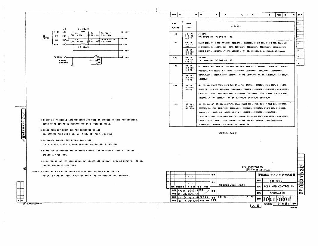
PCIA .... Ill
....
LS133O"")
"IlS6PI.TIE OTHERS AIlE THE SME AS - 03.
tt • "-----xI-----
---- ... -xf---
------x-------x-------xI----
-- ------x-------x-
" I·· I •r
• p .. ,T S
• I ..
01. RAil 1-330 I. I15ld.1KI. '"13301. RllI2OKI. IlIld.021t1. Rt1l2401. lP13ld.1I1. 111'1101.
1/22(2311. CII112OOl'1. C211100P1. C221100PI. C2311801' I. C2'12100PI. C32llsooPl.
C31ld. 1. 25VI. ClIld. 1. 25YI• .131141'1. J1ld1'l. JlIWI2P1. 1rV. 55. l3133OJl1. ld133Oo1lI.
RA1l7-3301. R514.7«1. ,"(3301. "(2.67«1. RU11201. I/13(2.21t1. Rlfll.2Itl. R22t2001.
CIBC2200P1. C2111l10l'1. C22IIOO1'I. C2'11801' I. C2l112100l'1. C32(lsooPI. <:3111.tL~VI.
CHII. I. 25VI. "31141'1. ""41'1. "Il\lUP). 1rV. ss. L3133OJl). L4133QJlI. l51330AIf'
"'(551'1.THE OlHERS AIlE THE SAME AS - Ot.
• S
SPEC.
,. tp I
S. S I DEE -STO
" tp I0.51 DE, -STO
,. tp I5.5 I DEE -510
411 tp I5.51 DE"-STO
41 tp I
0.5 I DE11-510
411 tp I5.5 I DE"-510
-03
-02
-0 I
-00--_.."..,..-.....-=-::--=-=,."....----[> 12v
'----------------t--+ OSV
'''SlOIl ~O---l-------O...FO_o-_-----+_~ TP5~ iDa
FI .... EGIOUNO a.
" tp ID. SIDE6-STO
01. 0'1. IJlL ""'11-'301. lPdld.1I1. ISld. Till. '"13301. RllI12KI. RIll. mI. 11111301.
lP13I,. 'II. 1111101. R221d54I. Cllll000Pl. C21l 21P I. C22121PI. C23IUloPl. C2l1110001'1.
C3010. 0022. 25VI. C31l0. 0022. 25vl. C3215e0l'1. C3S1100P1. <:31ld. T. 25VI. C38ld. T. 25vI.
"31141'1. "1141'1. ,,'IVI2pl. 1rV. St. L3118~1. ldllSO""'. lSII50J4)
-05 " tp IO. S I DE6'-SlO
VI. 01. 04. 0'1. IJlL 01. OIOIPHPl. CI.... '''111-'301. RA2....t21T-16IS-0tl. R21221l1.
17( 3301. 1181111 I. RlI2.7d«l. ItOld.4211. 11l12dOI. lP12ltJOI. RI313. tit I. IIltIIOIll.
1119ll0). 11121U21. C18110001'1. C2117S1'1. C22117P). C231 lOoP), C2tllOOOPI.
C3Q(O. 0022. 25vI. C31l0. 0022. 25V). C'2 I8lloP I. C:UIO. 022. 25vI. C:M115OOP1. C3S11001'1•
:>'•. SIGIIALS WITH 00U8LE "5TEIIIS.,I•• , ARE USED 01 CHUGEO III SOliE FOO HISlOIIS.
IEFU TO FO-S" TOTAL 01A1I.... no IT' S VUS I 011 TAILE.
S.POL ..1I11IlS lEY POSITIOII5 FOI/ COIlllECTOII,/) n!:
,/1: UTWEEI "'Id AIIO "'Ill. "4: 1'1113. ,/5: "'12. ",: Pili.
d. TOLEIANC. SYIIIlOLS FOI I. RA. C UO L ARE:
F:UI. 6:121. ":UI. It:ttOI. 11:1101. Y:.ZO~-IOI. l:.'0~-201
C'7(4. 7. 25VI. ClI14. 7. 25VI• .1311"''' .nISl'I. JlIJPI. "'IWUI'I. HGIlG!I/IIWlpl.
DCIIIYI SJP I. L3ItllO""l. L41110""'. LIltSO""I. !W
VERSION TABLE
3.C......CITOiHCI YAlUSES ARE III IIICIO FAR"OS. 10V 01 HIGHU. IIOllll. UILESS
OTHEIWISI SPECI F I DE.
II0HS: 1. PAIlS ,,\ TH All ASTEIISlI.' ARE OIFF£lEIIT II EACH PCIA HISIOII.
REHR TO W£ISlOII HillE. UIILlSTEO "'I/lS AI£ II0T U5EO \11 THAT \'£151011.
2.IUISTOIIl/I AIIO IUISTOI ARIAYlRAI VALUES AlE II OHIIS. I/IlV 01 GlUTEI. tSll,/1.
UlLESS OTHEIII15£ SPECIFIED.P/N-l5532060-XX -~
~(PC8 ISS~ A'-'E> ~__0
~,-_"".I---t----+---+--+---I ... TEAC '7.( ,,~ ? .. Jt~_~~
•• FD-55V ~Qt
I:--~t:t~ 0f--1;;;ti~iitiit••;t.-;-l";B1-_-+-~"~tr~11~"'~II)~X~...~Y1l~,(~"~"~II)~~~"'~ __-I -----L__ Elf e1ln., ." B •• "II ... PCBA MFO CONTROL UH I ('f)
- .... I~~ Itt· & • 7 R~ / all ...---11-----------1 ...
M" p _.~~=::_::_:__------------------------------------..L..:.:• ..::.:...L.:I)I!l'---~.lloo..J~~.•..Jbil.•..J,?...L..~_..J.._..J... ..L_._.._'__=':O::~S~Ci_H-E~Mi_AT~IC~:=_::~~ ••_ .It (.I:.. !!. 8S":.l ·2'1 .::. Ill. •• T B - E. .< ., I I I I..J I I I !
.s Jfl >~ Fl[.' /"'7 ....... -tu •• IO~m !u6l011i I
1§J10010230-o1 ~ 553C I 3. fIl7::':
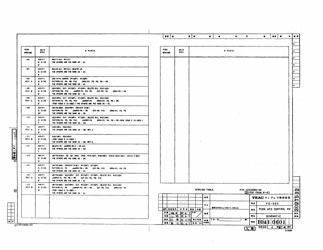
I
~ ·1· I E----•• a • a to r • ••• It ••
------)(
I-----
"CIA .... IM "CIA lIA,1I ------11 PARTS 11 pAIlTS x
~llJI!I 5p[C. VElISllJIS SPEC. I-------_.. -...-- x
-01 • up, RAU?-1I0• "'IIU. r--0.51 DE TIE 0TIE1IS AIl£ TIE !IoI'E AS - 01. ------I x
I----01 ..It" IlAUl-lln. "'IIK). lEt..El£ "3 ------
D.IIDE THE 0THE1IS AIl£ TIE !WlIE AS - 01. x
• I-----_._-
-011 .ltp, aM WITH.AM'£ll. I'I'I!i2PI. )(?C!i2PI xR[V. A D. II DE PATTEIIN:P2. .... .... PtO lJIEN:P1. n PS. ........ I--
• TIE 0THEIlS AIl£ TIE !WlIE AS - 01. _..----x
-01 .Itpi 010/lAiI. 511. I'I'C!i2PI. lCTI$2PI. lELm Itt1. 1l1211201 r-----IlEV .• 0.51 DE pATTEIIN: .... 1'10 .AM'£ll: Pl. n P5 0IT:P2. Pel lJIEN:", ......
• TIE OTHEIlS AIl£ TIE !WlIE AS - 01.
-01 .Itp I 0101..... ,. 511. 1'1'1!i2PI. lCTI$2PI. lELm Itt1. Itt21120 IIlEV. C 0.51 DE pATTEIIN:p1. PS. .... P10 .AM'£!l:P3 tI'EN:P2. .... PIS .....
1 IPCB 1SSl.E E 15 usm ) TIE OTHEIlS AAE TIE !WlIE AS - 01.
-01 IIItpl UllC?'LSOII. OlOIPNPI. aMCDlp SllEI
D. 5 I DE pATTEIIN:P2. Pel .AM'£!l:PIS ..... OIl: .... 1'10 tI'EN:p1. P1 P'5GF TIE 0THEIlS AAE TIE !WlIE AS - 05.
-10 lUl'l 0101..... ,. 511. I'I'I!i2PI. lCTl!i2PI. lELm 1tt1. 1l12C24010.5 I DE pAmllN:P1. PS. .... 1'10 .AM'£!l:P3 tI'EN:p2. .... ..... P8 IPCB ISSUE E IS U5£Q IF TIE OTHEIlS AIl£ THE s-E AS - 03.
-;;;:.- -II .8tp I 1I11111.). 1l22C~1
IlEV A O. 5 I DE THE OTHEIlS AAE TIE s-E AS - oe. IIEV. A.
~ •I:l.~ -II .ltp I 1I11111.,. 1l221~1,,-, IlEV. I D. S' I DE IPCB ISU E 15 usm. I
"".jI THE 0THEIlS AAE TIE SMo€ AS - oe. IIEV. C.
-12 IIII'; lEL£TE 1'1'. oAM'£RI.II-3 .. \.IlI-101ill 0.5 I DE THE OTHEIlS AAE TIE s-E AS - 03...J Ftil• -13 11Itp; UllI?'LSl32 I. 02. Q3. tIlAl. tIlA2. IlI1I1OOI. 111816801. C1210. 0221. 50\'1. C2?I•. ? 50\'1
.!. D. !II DE THE OTHEIIS AAE TIE s-E AS - 04.
lID G
-14 'Itp I U51?'LS08I. CIl4IDlp SllE I. 1/"(1521'1. lCTIS2PI.D. !j I DE pATTEIlII:P2. p. oAM'£R:'" .. P8 OIT:PI. 1'10 OPEN: PI. P1 PSII THE OTHEIlS AIlE THE s-E AS - 01.
-15 • IItP I UllI1'LS08). 0101..... ,. 511. 1'1'1521'1. lCTIS2PI. C£LETE IIll. 1l1211201 -IlEV. A D. 51 DE .,uF£1l:pl. P1 II!> ..... 0IT:P2. Pel. .... 1'10II THE OTHEIIS AIlE TIE s-E AS - 01 ----
-I !I '8tP I-_...-
U51?'LS08I. 0101..... ,. 51? 1/"(1521'1. lCTI$2PI. C£LETE 1111. 111211201llEv.8 D. !; I DE pATTEIlII:pl. P'5 ..uF£ll: 1'3. PIS .. PI 0IT:P9. 1'10 OPEN: 1'2. p, ---
~ II IPCB ISSlA! E 15 U5EO. I VERSION TABLEP/N ~5~6~~:A-E) -.ol
THE OTHEIIS AIlE THE SIIoIf: AS - 01 -- --~
~::... TEAC 7.( 1'':1 ?~Jt&t:l ..J.O.
--~.Jt FD-55V om.ttL -- 0i--- aTI1",lIlX." 911'('" )t";;~
I 2"1 l!UI.1J • " 9 IUt "II a .. PCB~ MFD CONTROL IH ~.... I~"" ~!".," . '7 R"/ Ill,. -- ...•• ,), 'U:. ~·6·7 ... SCHEMATIC ••II., J:. J}. IS':2 '1'1: _::.". ... T S - E___________________( II> lKli4!I! dad)ip ". VI :o(It Ill!." 6.. 7 •• ...., "t•• •• i16110010230-01 I I , ••• I I
II 5530\ 4 -'17=4: ••
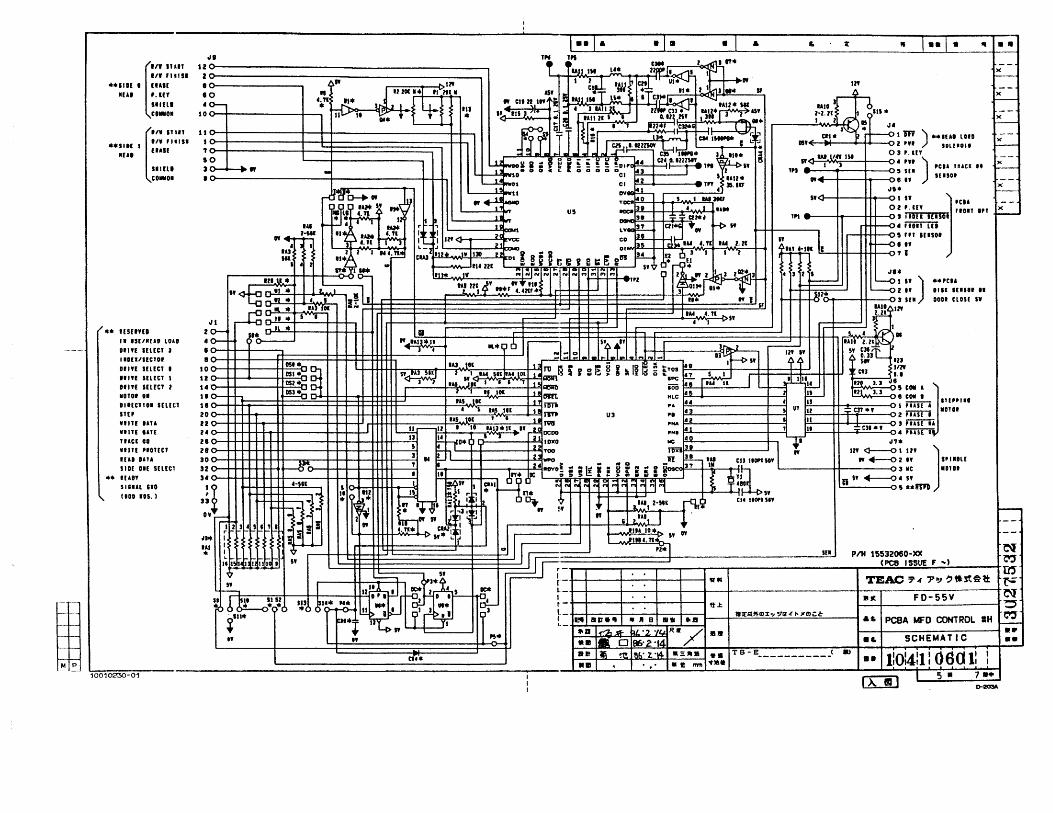
x
)(
)(
)(
~ ..
7.·5 •
•• •"
•• 1:0:4:1: 060 1: :
P/N 15532060-)0( N(PCS ISSUE F ~) t":1
m-TEAJ:; '7 -I ,,~ ~ 1!Ut iUl: F
IJJt FD-55V N-:;,.... PCBA MFD CONTROL IH t":J
••II" SCHEMATIC ••
., -
..
5[1
IIAIO,dl~.z-z.zi ~IS.I 1 JI&
J~" .I,ClU P 1m) -IUD LOID
05' _ Z P" toUI.II
W~lI" 1M 0 3 P.I('
'"~ "_ 'J -' P" ) PCIA TUtl ...--.---i--<>5 SlI
" _ II IT IlI'OI
",.0; :~m j:~::, IP1 )(,pt.---#--i+t-<>3 1I0ra HISOI
f-<>. ffiifTIi., I ..--H-++-OS ,n IfiSOI
II f-<>. "~a!..,,,..!." 1.i!1:-"-+++---H-++-O., I
..
In..
~~rI ."J. r-
" Ilt* •
1'f~ ~~: :.~;· IIC* l_
r&- I51' t- ttL...
r~.l .:[1:\,.,1)]:-; 91<JJ(" }ltf);:;~
FH"t I" II Ell ilIll •• • II B lilt ....L._
"II ~.Jf- I:.IL '7~ o/I..J. R_/ 1lIJ1
" all aD 96' 2. old._It4fi ~ I~,.. l. 0\4- .:::". ••
T 6 -E___________< II)c(••
• tl rrm v••.11 .
DH' ~051._
OSl':"
~-
I
~---.-511
I,'" I' tlZ. •
i~..... ~ :.... :...•~;I!I! "=:..........,,,s,
.I,[" ..." 12,..-
'" 'UISI 2""IIll. lUll •,..
~ " .. '19IIUI '.IU •0 " J II lOr •• ""''''111
Slllll •0-•. n II.
_! I J It-:• ~I'CO.OI so~ t f
C"'''u
." "1111 S,.. I
....11.1 IlUll ,
IIUIS 0
SlIUI 3o-~ .. .CO.OI •
....un'uII ISI/IIU. 10.0Dlnl IUlCT J11I1I/SECTOI., nl IHlCT •.IIYl SELECT 1OIlY( IHECl 1IIOTO••1
'!lrCtlOI flUtTIll'"IT'IA"nITt liltTUCI.OWI ITt PlOHCT
IU' 01"IlOl Oil Sll ltl
... trAIl'SllUl no1.00 '05. I
10010Z30-01
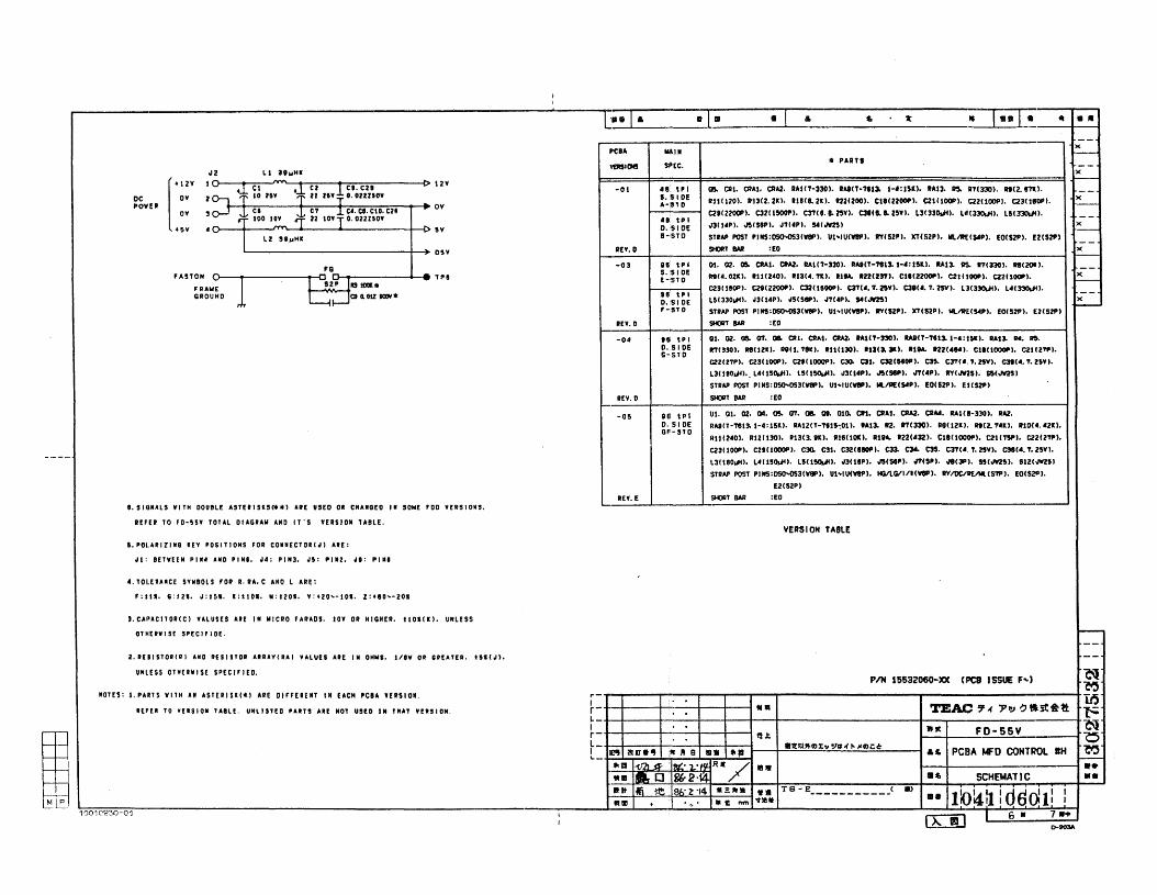
I. SlONALS WITH OOUIll! ASTEtlSIS<**) AI[ uno 01 CH ....O[D IN SOW[ '00 V[IlSIONS.
R£FER TO FO-S5Y TOTAL DIAGRAM AND IT'S VERSION TABLE.
, ASTOND-::_....... ......-0'60-_-----+--.- T;> I
I'RAWE 1 5Z' 13 iDOl *GROUND C3 Q.otz 1alV*
t> 12V
:: 5V
x-
VERSION TASlE
x-
x-
x-
)(
I---
• PARTS
xI---
x1---
VI. QI. 02. 01. os. fTI. os. 01. 010. at. CRA1. CRA2. CRAt. RAH8-3JO). 1112.
IIAilT-TeI3. 1-/1:1510. IIAI2IT-.,"S-,01). IAI3. 12. 1'1(330). Il8ClZIt). 11112. Tn). R1D('. '21t).
111112'0). 1112ClJO). 111313. 8!t). R16110ll). R1VA. 1221'32). CIIClOOOP). C211""". C22U'n').
C231100P). C2.UoooP). C3(), C31. C32<l'IOPI. cn ~ C3!1. C3Tlt. T. ZSV). C311'. T.l5VI.
L3I1S0~). L'USQaI4). LSCl5CUl). "3(161'1. "'(5eI'1. "'(Sl'I• .18(31'1. SS(.I't'2!1I. 5IZC.I't'2S)
STRAP POST PIMS:0SCNlS3CVllPI. Ul"'IIKWII'I. IGIlGll/lCwePI. RYItlC/I£I'llCS1P). EO(52l'1.
EZ(S2PI
SHOIlT BAR : EO
'-- •....JE:~~_.. .. 1: ~~. .._+-.-._t
lEY. E
L~ ..I'CIA "'-1.11PS1CH! SI'[C.
--01 "HI
S. 51 DEA-'T 0
'8. tillD. :SIDEI-;STO
lEY. 0
-03 U tP I5. '5 I DEE-STD
Ie tPI0.5 I DE'-5TD
lEY. 0
-0' lei tPI0.51 DEG-ST 0
lEV. 0
-05 III tP I0.51 DE0"-510
"---------------+-+ OSV
"2 Ll 3lh,HI[
1 o----;:r~C=-::I---',.,..... I C2 I c•. CU2 ,,, 10 25V +1' U flV to. DUlSOV
t-+-=---+-==--1-:-:~~~=-="""1~'"OV3 ,CI J, C'T .~C•• CG.Cl0.C2'• ~ i 100 I~ "T 22 10Y10' 022Z50Y
L2 3""HIe
[
+12V
OV
OV
+5V
DCPOWEll
I.POI.AlIZIM8 lEV POSITIONS FOR COUECTOII~1 AlE:
~I: SETWUH PlU AND PlHI. ~4: PIH3. ~5: 111M2. ~I: PI.,
4, TOLE lANCE SVMSDL 5 FOR I, RA. C AND L AlE:
':11'. G:12l. ~:HI, I:SIOI. 111:1201. Y:+20"-101. Z:+60""201
'.CAPAClTOR(CI ULUSES AlE IN MICRO FARADS. lOY Oil HIGHER. UOICI). UHLESS
OTNEIlII S£ SPEelf IDE.
2. RUISTORIII AND "ESISTOII AlRAVlRAI VALUES alE IN OHlll. Slew Oil GREATER. tSICJI.
PIN 15532060-)0( (PCB ISSUE F... )UNLESS OTH[IlIIS[ SPECH I ED.
NOTES: I. PAIlS WITH _N ASTEIISII>t1 AtE DIFFERENT IN EACH 'CIA VERSION.
IHEI TO VEISIOI TASLE. UNLISTED PARTS alE HOT USED IH THAT YERSION.
1f)O~C"230 01
N~
~-_:·:::::::::,·:::::::::::r-..-.--r---------.....,r--TE--AC--'7-;f-y-.,-.,-tl-~-*-~-t-·~~-- ;'~::~~~::-'---i---I---f ft..t. JJ Jt F0 - 55 y gt-tIl!ltAllii!ll;nu"ii.;lI!i1-;:.iA"IBiitiiillii.it;..!~i1--+J·!!1t~J;t~"'~CIJ~x!."'29!g!.('.t".!.".!!CIJ:f;:j:~:..-_--I.... PCBA MFD CONTROL IIH ~
.. a 1-(I2).if ~. 1.:w.. JU / IIl1 1----1------------1 ••lUI 1& IJ U2·14 II" SCHEMATIC ••• It Iii ~8h'2:'14 .=.JIl. 1tll TS-E -' II) II. l!n!,4"-, ',d~()i'lll ""III • ',,' lilt! rmI't!elJt 1\/":1:-'.1 0
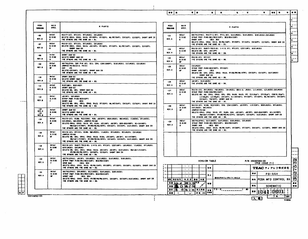
•• • • II • I • ~ t " 1··1 • - II •
--)(
t-
"CIlA ..... 111 !'CIA WAIN --SPEc. I: "AITS :II: "A.T' X
"BlIICM_KM
SP£C. ---
• stol IAICT-SU. nuu. "l.tVlI). UII"lSUU. IAllT·S. III. nU.51l. IUI.tVnl• SUI.tV2SI. IlIl.tVlSl.UIMtlX
-01 EOI".,O) '21 "UI I--D•• IDE DELETE :ClIAS. CIAI. 1A1S. ITI."I. ITt",.. III./IElS"l. EOIU"I. UISI'I. ilion IAt [0 D. SID£ snAP POST "'I:OCIIOCIIU". OCI/DUUW) --In.D I tilE onUI dE TIlE lAME &I - II. IEY.A I lMOIT IAt :OCI. DC. X
DELElE :CIAS. Clll. IAU. IElVLlS"'. IYIIlP). IT ISZ' I. UIS2P). [llszn llIOIT iii Et --OT 'IItO' .AIC.-tl). nltl). "1.tV"'. EOI.tV'O) TME OTMEIS AlE TME SAllE as - OS. --D.lIDE DELEtE :CltAI. Cill. 1111. "'11'''. "IU'I. lrTUl'). 111./1£1$4"1. EOlun ElIU". - )(
IU.D I ..., IWIIO -n tlto' IAll.·lltl. IA.It-tlU-fl. 1·':S.III. I1UII. CUIIOPI• 1111""'51 -Tilt: orlE" AIlE TIlE lAME AS • IS. D.IIDE DELEtE : CIS. CII. "IIS"I --IEr.a , TME OfMlIl AtE TME SAllE AS - 13. )(
-N .Ilttl I.I»T ....:0 f--D. SlDr DUUE:"" IWI EO -,. tlUI tall'-Ill. Itltl) --"Y.' • Till OflE" dE tilE IAIIE .. - 'I. O.IIDE TME OTMEII atE TME laM( A' • If. XIn.a llf --01 'Gttl UIIUUT... CUt ". Ill. IU. cu. CIIlSooon sUI.tVn). EtI""'Ol. ElI"'''1 .-D.IIDE "...I1:"...au·,. ,...£t -21 tlto' [OloIWZO)
"Y.' W CIT :P, D.5IDE Stu, I'OS1 PI1I5:OCIIS"). IYU")Dfl[1!:EOIIJtI). nlll'). IIlOIT ,AI [0 IlY. a • IIIOIT IAII :OCITIE orIElS dE tilE SAME AS • IS. DELEtE : OS. CII. CIAS. CltAl. lau. IYlOCnEIWlIITP). £DIU"). UIU". SU 1"'15 I
'UolIIIOIT IWI 10
-sa SIlOltT IAII:n THE OTHEII AlE Tit( 'AllIE AI - IS.D. SIDE DElUE:SIlOltT IWI EO
It!Y.• , tilE orlEII dE TIE SAllE AS • 13. I -n "UI ""3". 51'1""'SJO.IIDE TME OTHEIS AlE THE SAllIE AS ....
ott 'litol "lUll). '''I.nl IEY.a IIDo IIOE 5101T lWI:n i
11'.' I DflUI:., CltS. SIIOIT IA. EO i -21 'Ito' lAlli-III. ITloIWU •• FllINU). 111"'25). OIU-'. ""'SI. lIl""ZO). UI"'lO).EOIMIITIE DTIUS dE TIE 5A111 AS - '1. O. srDE SfU' !'OST PIIIS:OSOlDStI".,)
I 'E'. A • DELETE :0$. 0•• ClAS. CUl. CIS. CII. IAlO. UII. 11. CSUO,., I. CTUbl I. CillO. I)"•.-If .nol ...CI'). ElI.N1I1
ILtl3t~Il. L1l3l.... ). UU,,). UI"IVIVI'I. IYISI". XlIS"). III.lIfl"'I. filiI").
O. SIDE I'IIA' 1'011 PI ..I:oe'ISlP. nISI,.. FIISZ,.. '"I»T IAI £IlEY.' , SIIOI1 IAI :OC, TME OTHEIS atE THE SAllIE AS - Dt.
DELETI:" Cltl. CltAt. CltAl. IAII. XTISl' •• IIlIlEU"'. EtISZPI. EZIIl'" SHOIT IIA' EOtilE OTIIEIS AIlE Till lAME AS - n. I -zt IIttl lAlli-III. 'U'. IllIUIl. '". C341120DP). ",In,.. I/IIU". DsOI"nS). "1""'5l.
D. srDf fOC"",ol. SII""'!!)'11 'Iltol SIIOltT IAII:[2 I lEY.' I' "I.NI'EI:"",.IEY.C 0-1101 DflUE:11lOItT IWI lEO DELUE :Cllt. C'Al. ta... IT••saa. cu. ".UIP). oIIIIP•• DS'''OS'I'''''). OI ..IUf"").'11
lEY.' • TIE OTIlEIS AIlE TII£ SAME AS • ft. 'i HI/LG/I/Il""'••flOC/IENlIS"). EDISIPI. nIS1P). 512I""ZS). 5110rr III n
ntol IAll'-lU. ItH. IUIIH)••". "5157P). ITII£ OTHElI liE Tit( SAllE AS • n.
'11 DSOIM5I. IlGI"nll. lI.tVlS). "unS).O.IIDE £11M••• SUMS). ""'EI:P2~' ·21 ••tol Uln'LSUA). SlU""'5l. nu""zs). 11II""U)• EOI""'OI
lEW.' • OflUI:CIt.S. CIA!. latl. IT••ua. "SUIP). 18C"•• OIO"OSSI""'). fl"IUI"IPI. 0.1101 ITtAP POST "11I1:OCllOC'IU'). Del/DC.IIJII)IllVlUl/llvt,). IV/OCI'EIIIUS"). 10152' •• [2CSZPI. StlIMII. '1I01T IAt EI ! 'EY.' • SIIOIT IAI :OCl. DCI
Til! orllEltS dE Til! lAME AS .... DELEtE :ClAt. C'". ta... 1t1lll1S'''' IYCSlP). XT I U,.. EllSZ". ElISl". 5lJOIT III EI
~ THE OTMEIS AlE TME SAllIE AS • It.'11 • tt,1 IAlIl-tU. "fltll. Itn. ",IM5I• 11""21). "1""". 1£I".ZSI. EOI""'"
D. SIll " ...f.:P'....IEY.a w DflUE:.. Cltl. CltAS. CltAl. IAIS. .ua. "'UIP). "'IJlII. US ..IOI",,).
IllVlI'l/llvt'). 1Y/IC'IEIIlUIf"). rOIIZ". UII2'). IUIN211. IIIOIT IAI EITill OTIl£" dE TII£ SAME .. - ...
-tt 'U,I IAll.-1U.....n·TlII·OS. t-.:,. Ill. 11(til. CUUoP). LIIMSl. 11""'51. IYIMSI.Do 'lIE It51 ""SI. EOI"'20) i---IE,. a • DIL!1I:•• C111. ClAl. CltAZ. lASS. ,,'UIP). "IIIP). 'UC"'U). IIlVL"'''''v,,,.
ITlDCnEIWlCS"I. ElISlP). nlll,.. llIOlT lal U --Till GnUI AItE TIE IAIIE AI • IS. --
·ft 'Iltol UlI"L"..). ".UP). EOCoNIO). 5UIMS). SUI"''' •• "11".ZSl.~D. SIDE STtA' POST PlQ:OCSlDClIU',. OCS/OCleSW) VERSION TABLE PIM 1553Z0So-XXII'. a ,
'"I» IWI :OCI. DCI (PCB ISSUE F"') C":)DunE :ClAt. CIAI. Ull. 1E1IIl1S.PI. IYI.lPJ. XlIIl'J. £1111,.. UCIl,.. 1II01T IAt EO r-
InTill OfIlEII dE Till 'AIII! AI - n. I ." TEAC ~.( ."., ?JtiUI:r- r.:r--.~--n 'Uol UllTaLnUJ. UIMtl. SUC.tViS). SlUM5I. Stlln,,).
~D.IIDE ITIA' POIT PI .. :OCIIDCZIIJPJ. OCI/DClCIJP) I • lit FD-55VIn. a • IIIOltT ... :aez. aca t- !t.t 0l_DElEtE:CltAt. ClAl. tall. 1T11IC'1f.....1."). Etlll,.. (fCI")••ulnn). llIOIT 'AI EO I 1I1r.' .ll"J;l-'tD:I:~ !1II,f .. Jtl);:'~
.~ PCBA MFD CONTROL IH~Til OTIE" AItE Till lAME .. - ". L_ et .JlB •• ...... iob$l ~1.'~JU/ •• •••• lAo ",·z· .~ SCHEMATIC ••a. Il ~ BlJ·Z·J4. .::..-- TB - E__________ -< II)•• loalllaSolll I
•• ".. •• I•• • .... mil
10010230-01 I I 7 • 7"I
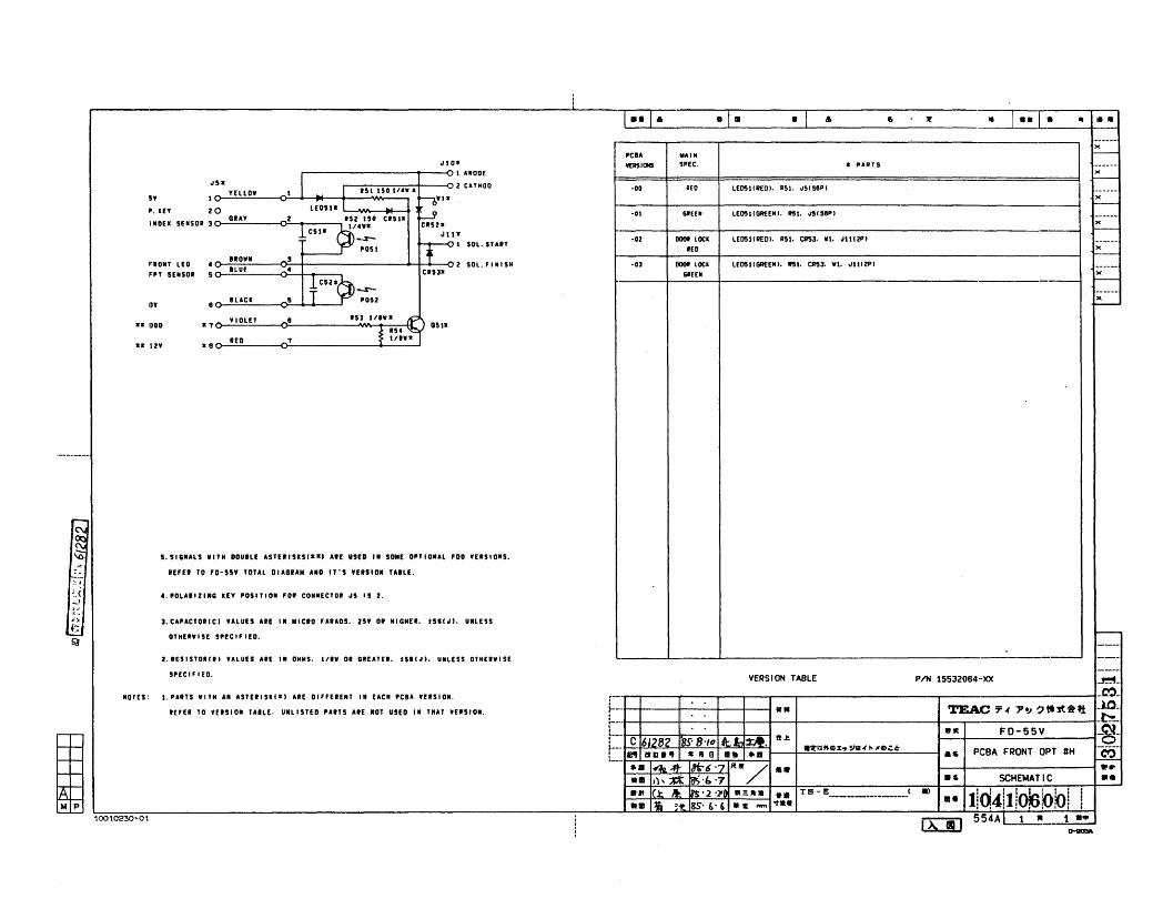
g.-- ·---LI_II ·_I__.. (, 1r ~1 • It • II
xf-----
xf-----PCBA MAIN
V[IlSICNS SPEC. a PARTS
-DO iEO LED5Il1IEO). R51. "5! SliP)
-ot : 61HII LED51IGREEN). lIS1. ",ISliP)
-02 QOOI LOCI LED5IlREO). R51. Cll53. "1. "lI12P)
lED
-03 QooI lOCI lED5I1GREEN). lIS I. CllS3. "1. ""HlP)
6IIHII~----+-----+-------------------------------
-sP052
153 II1"a ~<I,. 05111
~ tina
lcu.r
'" 1 oa'" t nODE
1 I 151 150 lIn a -.. 2 CATMODo---o.;~--~--+- .....~-+--.JV\/'wo---. h""
LE 05 ,a 1'---""'_--11...-.4C~=..:.-.__-o:2:....- .., 1S2 150 CIS111 W
L§/ua CIS211
CSla -s- "'11 a
P051 ~, SOL. START
o-7~----O:_3:....-1- .-.1-:.......'--0-2 SOL FIliI SH
• CIS 311
",sa
n 1- YElLO"~
P. lEY 20
'"0U SEIISOI 3-GUY
FIOIIT LEO .- BID""~
ILUEFPT SEIISOI 5
I). IIBLACI
:n 1)00 a7VI OLET
.a UV a8lED
5.SIGULS "ITH DOUIlE ASTElISUlaal alE usn II SOllIE OPTIOUL FOO VElSlOIlS.
IEFU TO FO-55\' TOTAL DIAGUM AID IT's .ElSIOI TAILE .
•. POlUllIIIG lEY POSlTlOII FOil COIIIIECTOI "5 IS 2.
3. CAPACTOIIICI VALUES alE III MICIO FAUOS. 25' 01 IIIGIIU. UII"I. UIlESS
OTHU" ISE SPEC I F I EO.
L .L- ..L- _
••554AT:=,.t. t
P/N 15532064-)Q(VERSION TABLE ~-
-"T.......,.---r---..-__- __--....---------......---.-----------f-~-
1~~::.~=~=====~=====:===:==~I__·-.._+_----------_I_-TEAC.......---'T-.f-y__'!J_'?_..__Jt_it_~__f~~• IHt FD-55V _~_
~~~:. c 6/282 :8S·B·,ol~Ir:I:2:'Jt. It.!: .1rI:afl.GlJ:.,Y~.(""G)':1: 0: IlltIlO." ."e •• "II A(, PCBAFRONTOPTIH I-as-'-" "II 142.~ at-6 '7 R._/ •• 1---1--. ... •
• 11 /1' hit 1st;'l:,'7 ... SCHEMATIC ••
2.IESISTOllil VALUES alE III OHMS. II'" 01 GIEATEI. UII"I. UIILESS OTH[IIIIISE
SPECI FlED.
1. PUTS "ITH All ASTElISIIII) ARE DIFFEII£IlT fl EACH PCIA 'ElSfOIl.
IEFEI TO VEISIOII TAiLE. UlIlISTED PAiTS alE lOT USED II THAT 'USlO•.
1I0TES:
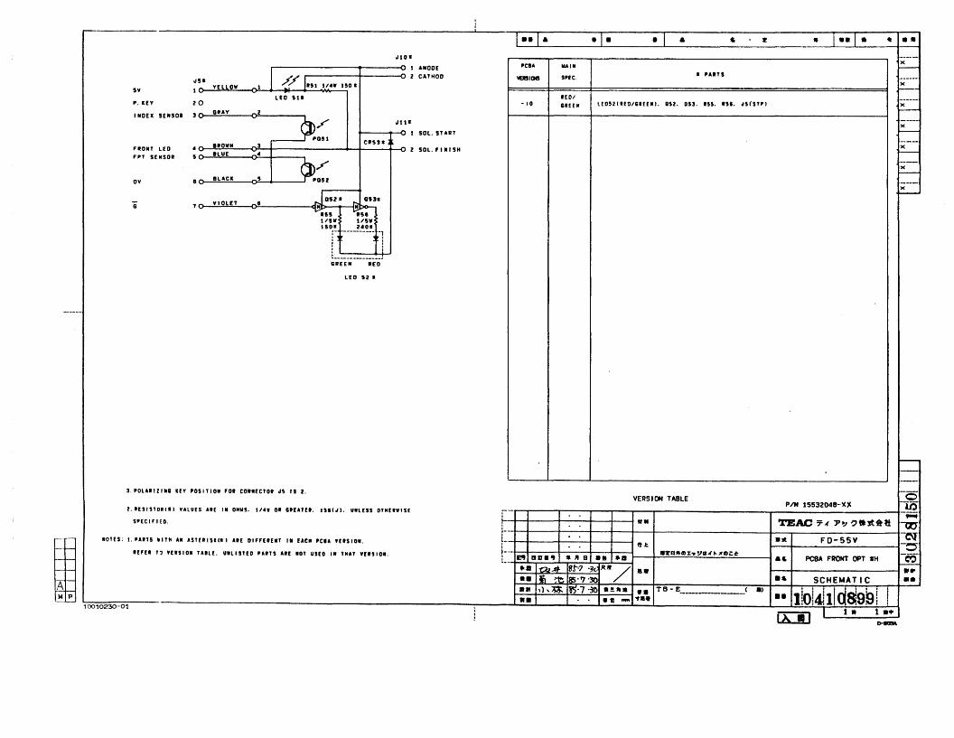
"5. .(/lu1 1/.W 150 IYELLOW 1$V 1 ~
LEO 511P. lEY 20
INDU 5£N50I ;,~ OIAY _2
/'P051
FIOIIT LEO • IIOWII ;,
FPT SENSOI S- ILUE •
OY I ILACK 5
G 7- YIOLET _I
II
1··1·.110.
1 AIIOOE PCIIA lUll
2 CATHOD VEIl!loe SPEC.
IEDI- 10 liEU
JU·
~ 1 SOL. START
CIS3. ,~ - 2 SOL. F I IISH
·1 •
LE05Zl1E0/8lUI" 052. DU. 15~. In. oI5(51P1
• T·· r• - • ..-----)(I-
----_..)(
~-
-----)(-----)(----)(
f--
--~
----~
OIEEII lEO
LEO 52 I
-
P/N 15532048-~)(
•• FD-55YIt..t1IT1l-.lDX.,YIl.r")l1l);:'1: ... PCBA FRONT OPT IH
•• ... SCHEMATIC
•• TB - E._____ -( II> • I • I I • • , I••• •• ]101411108991iXiJ I 1 • 1 ••
IHIG!A
VERS ION TABLE
.It \),~ IliIl';7'3D .=."... .......
.....~_.~~--~-~-~-~.. TEAC7~Y~?~~~ ~f~-'+--+---+--~--+----4---I--------~-..,.--------t-:-g
i-·· ~ aD.. • II B II. ".. I-~" .. In,A et'7 -:'k R_/ •••• •~ ~ 1R15'? -30 ••
2.I(sISTOIIII VALUES AlE 'N OHIIS. lin 01 GlUTEI. nlco/1. UILUS OTHU"'S(
SPECIFI£D.
3. POLAllZll; lEY 'OSITIOI FOI COIIECTOI .. ~ IS 2.
IOHS: I. PUTS IIITH .. ASTUlSlll' AlE OIFFU£I' .1 EACH 'CIA '£15101.
IEFU " '£15101 "'IU. VILISTED PUTS UE lOT USED II THAT 'USIOI.
10010230-01
TEAC CORPORATION3-7-3, Naka-eho, Musashino,Tokyo, JapanPhone : (0422) 53-1111
TEAC CORPORATION OF AMERICA7733 Telegraph Road, Montebello,California 90640, U. S. A.Phone: (213) 726-0303
• T'1 ::/) J~;jjtt~T -7°~ct~~ ~
• 70,ytO-'::;-"-{7.7 F'-517'
• /\ - I~ .::;-"-( 7.7 F' -51 7'
• T 7 l/ =:J 7"
• /~ - ') -t J['" =:J / t.0
.l - 7
• 1::::' T + l/ =:J 7"/J
• l/ - -tf - 1::::'T":tT" 1 A -) 7° l/ - ?
• -fr 11 -t ~./ -tt
• @: ::t;; tEE ~~ ~IJIL B
'1~¥&#l5--$*jj:B 180·** tB JR Ji. ~f rfJ ep HlT 3 - 7 - 3'8' "* g~ ~83 JR~!f (0422) 5 3 - 1 1 1 1 (ft)
*- :tnt '8' "*.ph 300· ± ;ffi rfJ "* w~ HlJ 1 1 - 5LlJ'*t:')[.,· ~8li ±;ffj(0298)24-2865Htl
*- ~ffi. '8'"*.ph 564·0R l1J rfJ ~ 7J\ HlT 3 - 34 - 10~83 7\.!l.& (06) 384 - 6 0 4 1 HtJ
-i; c5~'8'"*.Ph 464· ~ 6~mf HdR*tlli~ ') 3 - 2 - 3~83 1:; 6& (052) 782- 4 5 8 1 (ft)
It ~ '8' *-.ph 733· rz ~m 't' lZ 't! ,ff1 lET 10 - 24~8li rb.,% (082) 743 - 3 5 8 1 (ft)
t;w; ~ -g"*.ph 812·t~ Itri] f1j- t~ j; lZ *rr, 2 - 2 -- 24itt~3 NM~ (092) 441 - 3 6 0 0 ((\)
1t1J tJ '8' ,*.Pfr 980 ·1LlJ t r11 - ~ HlT 2 - 5 - 5cr5k. t:' )[.,·~83 1LlJ t (0222) 27 --1501H-IJ
tL ~Jt 8' *- ph 064·tL ~~ r11 ep 5k. r8: ~ 7 * f!§ 2 - 2<11't:. t:')i/~~litL~~(011 )521-4101({-t)
H L1J I ±~ 190-12·**fiBAri&HLlJrfJ1tJ*Sf-2-11 1~~3 iR~HtlJ (0425) 60- 3 2 1 1 (ft)
ArBj~=-I±~ 358·j~ I. ~ A Fe' m I)' :& tt3 8 5 7~83 Are' (0429) 62 - 7 1 5 1 (ftl


![RYR SRcd afS]ZT ^`gV^V_e - Daily Pioneer](https://img.dokumen.tips/doc/110x75/6328d06d051fac18490ee910/ryr-srcd-afszt-gvve-daily-pioneer.jpg)
![DecRZ_ eVde W`c R]] gV cVefc_VVd - Daily Pioneer](https://img.dokumen.tips/doc/110x75/6320224194d995f22f073f69/decrz-evde-wc-r-gv-cvefcvvd-daily-pioneer.jpg)


