Embed Size (px)
Citation preview
JOURNAL OF APPLIED PHYSICS 99, 014907 �2006�
Structural, morphological, and electrical characterization of heteroepitaxialZnO thin films deposited on Si „100… by pulsed laser deposition:Effect of annealing „800 °C… in air
S. M. Jejurikar, A. G. Banpurkar, A. V. Limaye, S. K. Date, S. I. Patil, and K. P. Adhia�
Centre for Advanced Studies in Solid State Physics and Materials Science, Department of Physics,University of Pune, Pune 411 007, India
P. Misra and L. M. KukrejaThin Film Laboratory, Centre for Advanced Technology (CAT), Indore 452 013, India
Ravi BatheInternational Advanced Research Center for Powder Metallurgy and New Materials (ARCI),Hyderabad 500 005, India
�Received 29 June 2005; accepted 2 December 2005; published online 13 January 2006�
Pulsed laser deposition technique was used for growing thin films of ZnO on Si �100� substrate heldat different temperatures �Ts�. All the as-deposited films have shown a preferential c-axis orientationassociated with varying grain size as a function of Ts ranging from 100 to 600 °C. Current-voltage�I-V� characteristics of these films show Ohmic behavior over the entire Ts range studied. Thesefilms were subjected to annealing at 800 °C in air ambient for 4 h. The grain size was observed toincrease after the annealing process for all the films deposited at different Ts. Interestingly, theseannealed films show nonlinear variation of current with applied voltage, very similar to the oneobserved in doped ZnO varistors. The nonlinear parameters such as the asymmetric behavior ofchange in current on the polarity reversal of voltage, the plateau region, and the break down voltageare observed to depend on Ts. This nonlinear behavior can perhaps be explained on the basis ofelectronic conduction model proposed for the bulk, doped ZnO varistors. The role of insulatingintergranular layers between the disoriented microcrystallites is expected to be similar to that playedby insulating intergranular layers in the doped ZnO varistors. © 2006 American Institute of Physics.�DOI: 10.1063/1.2160713�
I. INTRODUCTION
Realizing ZnO in highly oriented/epitaxial thin-filmform is currently a subject of active research interest. Thisinterest stems from the fact that ZnO is a potentially impor-tant material for different applications in fields such as opti-cal, electrical, piezoelectrical, optoelectrical devices,1–3 etc.With the demonstration of laser action in the ultraviolet �UV�range,4 the utility of ZnO thin film has been extended wellinto the regime of optoelectronic devices. Furthermore, thelattice mismatch between ZnO/GaN and ZnO/AlN is�1.94% and 4.31%, respectively, suggesting that the thinfilms of ZnO could be ideal buffer layers for the epitaxial/highly oriented growth of III-V wide-band-gap semiconduc-tor films, for which no suitable low cost substrates are pres-ently available.5 However in such applications, it isimperative to grow good quality thin films of ZnO especiallyon substrates of the most used electronic material, i.e., sili-con �Si�, albeit it is totally lattice mismatched. Many tech-niques have been used to synthesize thin films of ZnO.Pulsed laser deposition �PLD� technique has emerged as aviable technique for the growth of ZnO thin films due to itsvarious advantages, viz., �a� the ability to reproduce the sto-
a�Author to whom correspondence should be addressed; electronic mail:
[email protected]0021-8979/2006/99�1�/014907/7/$23.00 99, 01490
Downloaded 17 Jan 2006 to 196.1.114.240. Redistribution subject to
ichiometry of the target materials under optimized depositionconditions, �b� an inherently clean process with significantdegree of parameter freedom, etc.
We deposited thin films of ZnO on Si �100� substratesusing PLD under optimized conditions. In this study, we ex-amine �i� the role of Ts from 100 to 600 °C, maintained dur-ing deposition, and �ii� the effect of annealing of these filmson the structural as well as electrical properties. Significantvariations have been observed in these properties of the as-deposited �AD� films and annealed �A� films. Observation ofnonlinearity in the I-V characteristics of the A films whencompared to the linear relationship for AD films is one of themajor outcomes of annealing. The significance of Ts duringdeposition is also reflected, rather prominently, in the nonlin-earity of the A films. Attempts have been made to correlatethe effect of Ts and subsequent annealing on the size, polar-ity, and orientation of ZnO microcrystallites.
II. EXPERIMENTAL DETAILS
Excimer laser �KrF gas; wavelength �=248 nm, pulseduration tp=20 ns, repetition rate=5 Hz� was used for theablation of ZnO target. Laser radiation was focused onto thetarget mounted in a deposition chamber. The polar angle be-tween the incident radiation and the normal to the surface ofthe target was 45°. The target was rotated continuously at
10 rpm to avoid texturing/pitting of the surface during depo-© 2006 American Institute of Physics7-1
AIP license or copyright, see http://jap.aip.org/jap/copyright.jsp
014907-2 Jejurikar et al. J. Appl. Phys. 99, 014907 �2006�
sition. The fluence of the incident radiation on the targetsurface was kept at 2.0 J /cm2. Prior to mounting the Si �100�substrates into the deposition chamber, they were degreasedultrasonically, first in CCl4, then in acetone, and finally inmethanol for 5 min each and then dried under nitrogen gasjet. No attempts were made to etch out the native oxide layerexisting on the surface of Si substrates. These substrateswere mounted on a heater and placed parallel to the target ata distance of 7 cm. The deposition chamber was evacuated toa base pressure of �1�10−5 Torr. High-purity �99.95%�oxygen was introduced into the chamber to the desired pres-sure of 1�10−4 Torr, and maintained constant throughoutthe deposition. Depositions were carried out at different Ts
ranging between 100 and 600 °C. The substrates with thedepositions were slowly cooled to room temperature underthe same oxygen pressure before taking out for investiga-tions. Two sets of films were deposited under identical con-ditions. One of the sets was annealed at higher temperatureof 800 °C in air ambient for 4 h. For the present work, wefocus our attention on films deposited at 100, 300, and600 °C. Samples deposited at the intermediate temperaturesare observed to follow the trend and hence are not shownhere. Suffixes 1, 3, and 6 following AD films and A filmsrefer to the samples deposited at 100, 300, and 600 °C, re-spectively, in both cases.
The thickness of the films was measured by Tally step.The structural properties of the films were investigated bymeasuring x-ray-diffraction peaks’ widths �full width at halfmaximum �FWHM�� of the in plane reflections in �-2� scanmode and in a direction normal to the diffracting planes inthe �-scan mode both being recorded in the Bragg geom-etries. In both the measurements, Ni-filtered Cu K� radiationat 1.542 Å was used. The surface morphology and crystallitesize of ZnO in the films were recorded by atomic force mi-croscopy �AFM�. The I-V characteristics were recorded forthe AD films and A films using the four-point probe resistiv-ity measurement method.
III. RESULTS AND DISCUSSION
A. Thickness variation
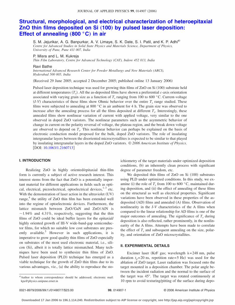
Figure 1 shows the thickness of the films as a function ofTs. It is observed that the thickness of the film deposited upto Ts=300 °C is �3000 Å. For Ts�300 °C the thicknessreduced drastically. At Ts=600 °C it is �500 Å. This reduc-tion in thickness with the increase in substrate temperature isexpected. The vapor pressure of Zn is high and increasesrapidly with the increase of temperature, resulting in re-evaporation of the Zn atoms from the substrate before beingoxidized.6,7 The oxygen pressure in the deposition chamber,as mentioned earlier, is maintained at 1�10−4 Torr, whichmay not be sufficient to oxidize all the metal atoms/ionsarriving on the surface of the substrate. At around300–350 °C, oxygen also starts to reevaporate from the sur-
face.Downloaded 17 Jan 2006 to 196.1.114.240. Redistribution subject to
B. Structural analysis by XRD
The x-ray-diffraction study was carried out in two scan-ning modes ��-2� and � scans� in the Bragg geometry.
1. �-2� scan
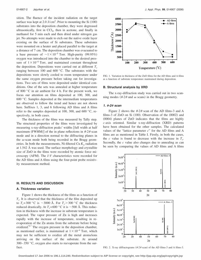
Figure 2 shows the �-2� scan of the AD films-3 and Afilms-3 of ZnO on Si �100�. Observation of the �0002� and�0004� planes of ZnO indicates that the films are highlyc-axis oriented. Similar x-ray-diffraction �XRD� patternshave been obtained for the other samples. The calculatedvalues of the “lattice parameter c” for the AD films and Afilms are as mentioned in Table I. Firstly, in both the cases,the c value is found to decrease with the increase in Ts.Secondly, the c value also changes due to annealing as canbe seen by comparing the values of AD films and A films
FIG. 1. Variation in thickness of the ZnO films for the AD films and A filmsas a function of substrate temperature maintained during deposition.
FIG. 2. X-ray diffractograms ��-2� scan� of the AD films-3 and A films-3.
AIP license or copyright, see http://jap.aip.org/jap/copyright.jsp
the deposition was done.
014907-3 Jejurikar et al. J. Appl. Phys. 99, 014907 �2006�
Downloaded 17 Jan 2006 to 196.1.114.240. Redistribution subject to
deposited at similar temperatures. The films deposited at300 °C have a c value very close to the theoretical value�5.204 Å� and hence has been selected as reference for com-parison. Films with c values greater than the theoreticalvalue �Ts�300 °C� show +ve or extensive strain where asthose with lower values �Ts�300 °C� show −ve or compres-sive strain. In case of A films, all the samples show −ve orcompressive strain, i.e., the films deposited at Ts=100 °Cshows extensive strain, but after annealing all the films showcompressive strain.
Decrease in the FWHM�2�� of the �0002� peak of ZnOindicates �a� the enhancement in the crystallite sizes of ZnOwith the increase in Ts and �b� increase of the crystallite sizedue to annealing when compared to the as-deposited films.Thus, the highly distorted ZnO crystallites grown at 100 °Cshow FWHM�2�� of 0.48°. For the AD films-3, this value isminimum, i.e., 0.18°. For the A films specifically A films-3and A films-6, the minimum value of FWHM�2�� is obtainedas 0.16°. The FWHM�2�� of the �0002� peak relates inverselyto the size of the coherent scattering regions �CSR� in direc-tion parallel to the diffraction planes.8 The CSR size is �45and �52 nm for the AD films and A films deposited at300 °C, respectively. Hence, annealing shows noticeable im-provement in the crystalline quality of the films compared tothe AD films.
2. � scan
The growth of the mosaic blocks of ZnO on Si �100�would be greatly influenced by the large differences in the �i�lattice constants, �ii� crystallographic structures, and �iii�thermal expansion coefficients of Si and ZnO. This can resultin the bending of blocks and appearance of different defects/distortions specifically at the substrate-film interface.8 Theeffects of microdisorientations of the diffracting planes and
d c values, the estimated percentage strain, and thes and A films from the recorded XRD ��–2� scan�
MAD
�
c valuefor Afilms��
Strain in Afilms�%�
FWHM �0002� Afilms�deg�
5.182 −0.422 0.235.182 −0.422 0.165.178 −0.499 0.16
TABLE II. This shows the comparison between FWHM of the �0002� peaksof ZnO for both the AD films-1, -3, and -6 and A films-1, -3, and -6,respectively, from the recorded XRD �� scan� patterns.
S. No.Substrate-temp. �Ts�
�°C�FWHM �0002� AD
films �deg�FWHM �0002� A
films �deg�
1 100 8.18 7.942 300 1.80 1.173 600 2.14 1.89
TABLE I. This shows the comparison between calculateFWHM of the �0002� peak of ZnO for both the AD filmpatterns.
S. No.
Sub.temp.�Ts��°C�
c valuefor AD films
��
Strain inAD films
�%�
FWH�0002�
films�deg
1 100 5.258 1.037 0.482 300 5.204 ¯ 0.183 600 5.188 −0.307 0.22
FIG. 3. X-ray diffractograms �� scan� of the AD films and A films in theBragg geometry. The suffixes 1, 3, and 6 after AD films and A films denotethe substrate temperature, viz., 100, 300, and 600 °C, respectively, at which
AIP license or copyright, see http://jap.aip.org/jap/copyright.jsp
014907-4 Jejurikar et al. J. Appl. Phys. 99, 014907 �2006�
the CSR in the direction normal to the diffracting plane arereflected in the broadening of the XRD peaks �0002� re-corded in the Bragg �-scan mode.
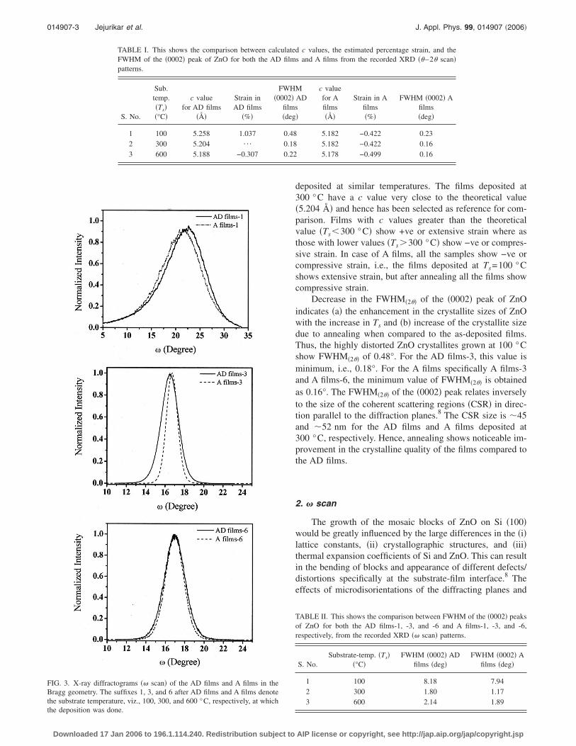
Figure 3 shows the x-ray diffractograms recorded in theBragg �-scan mode for AD films-1, -3, and -6 as well as Afilms-1, -3, and -6, respectively. Table II gives the FWHM����values for the AD films and A films. From Table II and Fig.
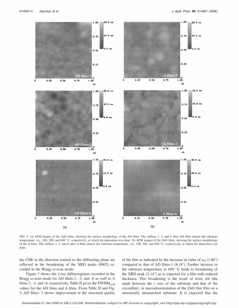
FIG. 4. �a� AFM images of the ZnO films, showing the surface morphologtemperature, viz., 100, 300, and 600 °C, respectively, at which the depositioof the A films. The suffixes 1, 3, and 6 after A films denote the substrate tedone.
3, AD films- 3 shows improvement in the structural quality
Downloaded 17 Jan 2006 to 196.1.114.240. Redistribution subject to
of the film as indicated by the decrease in value of �� �1.80°�compared to that of AD films-1 �8.18°�. Further increase inthe substrate temperature to 600 °C leads to broadening ofthe XRD peak �2.14°� as is expected for a film with reducedthickness. This broadening is the result of twist, tilt �theangle between the c axis of the substrate and that of thecrystallite�, or microdisorientation of the ZnO thin film on a
the AD films. The suffixes 1, 3, and 6 after AD films denote the substrates done. �b� AFM images of the ZnO films, showing the surface morphologyture, viz., 100, 300, and 600 °C, respectively, at which the deposition was
y ofn wampera
structurally mismatched substrate. It is expected that the
AIP license or copyright, see http://jap.aip.org/jap/copyright.jsp
014907-5 Jejurikar et al. J. Appl. Phys. 99, 014907 �2006�
quality of the films would improve with thickness of thefilms. However, this broadening, when compared to that ofthe film deposited at 100 °C is much lower suggesting im-provement in the quality of the ZnO films even at reducedthickness of less than 1000 Å. From Fig. 2 and Table I, it canbe seen that the films deposited at 300 °C are of superior
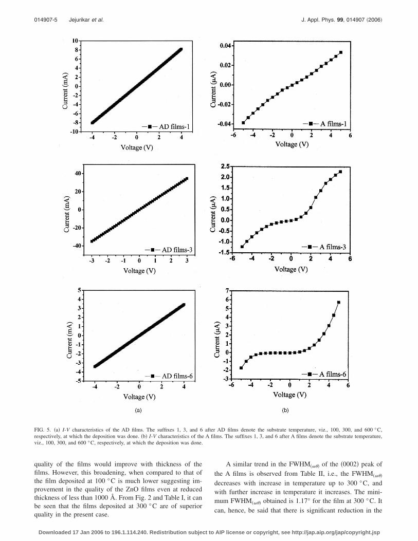
FIG. 5. �a� I-V characteristics of the AD films. The suffixes 1, 3, and 6respectively, at which the deposition was done. �b� I-V characteristics of theviz., 100, 300, and 600 °C, respectively, at which the deposition was done.
quality in the present case.
Downloaded 17 Jan 2006 to 196.1.114.240. Redistribution subject to
A similar trend in the FWHM���� of the �0002� peak ofthe A films is observed from Table II, i.e., the FWHM����
decreases with increase in temperature up to 300 °C, andwith further increase in temperature it increases. The mini-mum FWHM���� obtained is 1.17° for the film at 300 °C. Itcan, hence, be said that there is significant reduction in the
AD films denote the substrate temperature, viz., 100, 300, and 600 °C,ms. The suffixes 1, 3, and 6 after A films denote the substrate temperature,
afterA fil
AIP license or copyright, see http://jap.aip.org/jap/copyright.jsp
014907-6 Jejurikar et al. J. Appl. Phys. 99, 014907 �2006�
tilt, twists, and micromisorientations of the grains as the sub-strate temperature is increased from 100 to 300 °C �A films-1 and -3�. If the substrate temperature is further increased to600 °C, then the FWHM increases slightly suggesting againthat in the present case, the films deposited at 300 °C are ofsuperior quality. It can thus be said that the A films are ofsuperior quality.
C. Surface morphology by AFM
Figures 4�a� and 4�b� show the surface morphology ofthese samples as seen by atomic force microscopy. The mi-crographs in Figs. 4�a� show the effect of substrate tempera-ture on the grain size for the AD films-1 -3, and -6, whereasFigs. 4�b� show the micrographs of the A films-1, -3, and -6.From Figs. 4�a� it is seen that �a� the grain size increaseswith substrate temperature up to 300 °C. Further increase inthe temperature decreases the size of the grain �as well as thethickness of the films in Fig. 1� and �b� the surface roughnessof the film decreases with the increase in temperature. Oncomparing the micrographs of AD films-1 and A films-1, theenhancement of the grain size is clearly observed. This sup-ports our earlier analysis of the x-ray diffractograms,wherein the decrease/increase in FWHM�2�� �Table I� of thecorresponding XRD peaks was correlated to the increase/decrease of crystallite size. Similar trend is seen for the othersamples as well.
D. I-V measurements
Figures 5�a� and 5�b� show the I-V characteristics for theAD films and A films, respectively. In the case of AD films�Fig. 5�a��, all the samples, deposited at different Ts, showedlinear dependence of current on applied voltage, which is atypical Ohmic behavior. This linear I-V behavior is in agree-ment with that suggested by Gupta9 for pure �no additivessuch as Bi2O3 and transition-metal oxides are present� non-stoichiometric, n-type conducting ZnO. Our samples alsoshow n-type conductivity with a carrier concentration of�1019 electrons/cm3. The cause of this n-type conductivityis being debated widely. While Look et al.10 and Kohanet al.11 strongly suggest that Zn interstitial is the dominantnative shallow donor in ZnO and not oxygen vacancy, Vande Walle12 and Van de Walle and Neugebauer13 strongly ad-vocate the role of hydrogen in ZnO as a source for conduc-tivity. After annealing, it is seen that all the samples becomehighly insulating. Five orders of magnitude increase is seenin the A films when compared to the AD films. InterestinglyI-V characteristics of these annealed films show non-Ohmicbehavior very similar to the one observed in bulk, �Bi2O3
+transition oxide�-doped ZnO varistor.9,14 It is well knownthat the nonlinearity in bulk ZnO varistor is a grain-boundaryphenomenon where a barrier to majority carriers, i.e., elec-trons, exists in the depletion region of adjacent grains.9,14,15
During the annealing process, the incorporation of oxygenfrom the ambient might help in saturating the defects at thegrain boundaries as well as in decreasing the concentrationof oxygen vacancies or related defects within thecrystallites.16 This could lead to oxygen ion gradient gener-
ating the potential barrier between the two adjacent grains.Downloaded 17 Jan 2006 to 196.1.114.240. Redistribution subject to
Secondly it is seen from Figs. 4�b� that annealing also helpsin the growth of the grains thus reducing the number of grainboundaries. The combined effect of reduction in oxygen va-cancies and the grain growth results into ZnO crystallitesbeing separated from each other by an insulating grainboundary. This insulating oxide layer sandwiched in betweenthe two grains could be responsible for the nonlinear re-sponse in the I-V measurements.
The effect of substrate temperature maintained duringdeposition is found to influence the I-V characteristics of theA films-1, -3, and -6 rather significantly. From Fig. 5�b�, it isinferred that as the substrate temperature increases �a� thenonlinearity and breakdown voltage are found to increase,�b� the resistivity of the thin film is also observed to increase,and �c� the A film -6 shows inhomogeneity in the I-V char-acteristics, i.e., the change in current in asymmetric to thereversal of polarity of the applied voltage. The importance ofthese results is that this nonlinearity is observed in samplesthat are single-phase, highly oriented ZnO films without anyadditives.9,14,15
IV. CONCLUSION
In conclusion, highly textured, c-axis-oriented ZnO thinfilms were deposited successfully on Si �100� substrates withnative SiO2 layer. The epitaxial relationship is ZnO �0001�//Si�100� substrates. The x-ray-diffraction studies in �-2� andthe � scan clearly show that A films are of superior quality interms of increased sizes of CSR, decrease in c-axis misalign-ment, and reduction in twist and micromisorientations of thegrains compared to AD films. Even though the A films aresuperior to AD films, the effect of Ts maintained duringdeposition dominates the quality of the thin film. The atomicforce micrographs indicate �a� the growth of the crystallitesas a function of substrate temperature and �b� the growth ofZnO crystallites on annealing the as-deposited films, in linewith the findings of the XRD analysis. The nonlinearity inI-V characteristics of A films suggests the use of PLD-grownthin films subjected to annealing as thin-film varistors inelectronic industry.
ACKNOWLEDGMENTS
The authors would like to thank DAE-BRNS for the fi-nancial support extended for carrying out this work under theproject sanction No. 2002/34/21/BRNS. We would also liketo thank Dr. Lalla and Dr. T. Ganeshan from IUC-DAEF,Indore for their help with XRD and AFM experimentation.
1S. J. Pearton, D. P. Norton, K. Ip, Y. W. Heo, and T. Steiner, J. Vac. Sci.Technol. B 22, 932 �2004�.
2Z. L. Wang, Mater. Today 7, 26 �2004�.3D. M. Bagnall, Y. F. Chen, Z. Zhu, T. Yao, M. Y. Shen, and T. Goto, Appl.Phys. Lett. 73, 1038 �1998�.
4D. M. Bagnall, Y. G. Chen, Z. Zhu, T. Yao, S. Koyama, M. Y. Shen, andT. Goto, Appl. Phys. Lett. 70, 2230 �1997�.
5R. D. Vispute et al., Appl. Phys. Lett. 70, 2735 �1997�.6S. H. Bae, S. Y. Lee, B. J. Jin, and S. Im, Appl. Surf. Sci. 154–155, 458�2000�.
7Semiconducting Transparent Thin Films, edited by H. L. Hartnagel, A. L.Dawar, A. K. Jain, and C. Jagadish �Institute of Physics, London, 1995�,p. 116.
8
V. Ratnikov, R. Kyutt, T. Shubina, T. Paskova, E. Valcheva, and B. Mon-AIP license or copyright, see http://jap.aip.org/jap/copyright.jsp
014907-7 Jejurikar et al. J. Appl. Phys. 99, 014907 �2006�
emar, J. Appl. Phys. 88, 6252 �2000�.9T. K. Gupta, J. Am. Ceram. Soc. 73, 1817 �1990�.
10D. C. Look, J. W. Hemsky, and J. R. Sizelove, Phys. Rev. Lett. 82, 2552�1999�.
11A. F. Kohan, G. Ceder, D. Morgan, and C. G. Van de Walle, Phys. Rev. B
61, 15019 �2000�.Downloaded 17 Jan 2006 to 196.1.114.240. Redistribution subject to
12C. G. Van de Walle, Phys. Rev. Lett. 85, 1012 �2000�.13C. G. Van de Walle and J. Neugebauer, Nature �London� 423, 626 �2003�.14L. Wang, W. Wu, X.-G. Li, and Y. Zhang, J. Appl. Phys. 77, 5982 �1995�.15S. Tanaka and K. Takahashi, J. Eur. Ceram. Soc. 19, 727 �1999�.16Y. F. Lu, H. Q. Ni, Z. H. Mai, and Z. M. Ren, J. Appl. Phys. 88, 498
�2000�.
AIP license or copyright, see http://jap.aip.org/jap/copyright.jsp


