Embed Size (px)
Citation preview
This document is downloaded from DR‑NTU (https://dr.ntu.edu.sg)Nanyang Technological University, Singapore.
Statistical characterization and reliabilitymodeling of novel high‑K gate dielectric stacks
Nagarajan Raghavan
2012
Nagarajan Raghavan. (2012). Statistical characterization and reliability modeling of novelhigh‑K gate dielectric stacks. Doctoral thesis, Nanyang Technological University, Singapore.
https://hdl.handle.net/10356/50738
https://doi.org/10.32657/10356/50738
Downloaded on 12 Feb 2022 15:36:04 SGT
Statistical Characterization and Reliability Modeling of Novel High-κ Gate Dielectric Stacks
NAGARAJAN RAGHAVAN
School of Electrical & Electronic Engineering
A thesis submitted to the Nanyang Technological University
in partial fulfillment of the requirement for the degree of
Doctor of Philosophy
2012
NA
GA
RA
JAN
RA
GH
AV
AN

i
Dedicated
To My
Beloved Grandfathers
MR. S.N. SIVARAMAKRISHNAN
(Bangalore, India)
& MR. S. NARAYANASWAMY
(Chennai, India)

ii
AAACCCKKKNNNOOOWWWLLLEEEDDDGGGEEEMMMEEENNNTTTSSS
I am deeply indebted to my supervisor Prof. Pey Kin Leong, for his constant guidance,
encouragement, friendly informal interactions and technical support throughout the course of this
research work. His stimulating ideas, fruitful discussions, immediate feedback and unparalleled
patronage have helped me a lot in achieving my results. He has been much more than a
supervisor in motivating me and shaping my future in the right way. I have always found him as
the right person to talk to regarding all matters that are both personal and professional. It has
been an exciting and very satisfying journey for me all through my Ph.D. candidature and I
consider myself very fortunate to have worked under such a nice person. I would like to take this
opportunity to express my sincere gratitude to him for all the freedom and flexibility he gave me
in planning and carrying out my work. Thanks a ton sir! I hope I can be at least half as hard working
and diligent as you when I join the academia in the future.
My parents Dr. Nagarajan and Mrs. Srimathi Nagarajan have also been a great source of
emotional support and inspiration to me throughout my career and it is their love and affection
that has always kept me moving forward. I had a very conducive atmosphere at home that
enabled me to work efficiently at odd times when required. All my family members (aunts,
uncles and cousins) and closest friends (Anay & Omkar) have also been a strong pillar of support
and avenue for refreshing myself. Their interactions always kept me recharged from time to time.
My thanks to Dr. Michel Bosman of the A*STAR Institute of Materials Research and
Engineering (IMRE), previously at the A*STAR Institute of Microelectronics (IME), for his
technical guidance during the group meetings. He has helped me a lot in reviewing my
conference and journal manuscripts prior to submission and his materials knowledge has helped
iii
a lot in this work. I would like to acknowledge Asst. Prof. Yu Hong Yu for kindly agreeing to be
the co-supervisor for this project, Prof. Ang Diing Shenp for granting access to probe stations
and characterization setup in the SC2 Lab and Mr. Chow Kam Wah for his technical support.
Thanks to all members of the Gate Oxide Reliability Research Group at NTU, headed by
Prof. K.L. Pey. We have had technical discussions and debates on many occasions and our
brainstorming sessions have always helped each other in progressing with the objectives of our
work. The greatest strength of our group lies in the internal collaboration and support that we
members have for each other. Li Xiang, Wu Xing (TEM support), Shubhakar (STM analysis) and
Wenhu (Prober training) have been very helpful at various phases of my work. I would like to
thank my closest friends Anson, Shubhakar and Beng Sheng for their support as well. We have
had lots of fun meeting for lunch and chit-chat sessions at the canteen almost everyday.
The samples support provided by our collaborators at the Interuniversity Microelectronics
Centre (IMEC), Belgium (Dr. Thomas Kauerauf) has been extremely useful. Reliasoft® Inc. has
helped us by providing licensed access to reliability software tools. This work is sponsored by
the Ministry of Education (MOE), Singapore Grant No. T206B1205 and NTU RGM 33/03.
I would like to acknowledge our collaborators Prof. Luca Larcher and Dr. Andrea Padovani
of the University of Modena et Reggio Emilia, Italy for the useful teleconference discussions on
modeling and simulation we have had on numerous occasions during the course of this project.
Above all, the blessings of my late grandfather, Mr. S.N. Sivaramakrishnan, have always
been with me and I will always cherish the moments I have spent with him. There is no doubt in
that, had he been here, he would have been the happiest person to celebrate my completion of
doctoral studies today. I really miss him on such an occasion and I thank the almighty for giving
me such a Golden Grandpa!!!
iv
TTTAAABBBLLLEEE OOOFFF CCCOOONNNTTTEEENNNTTTSSS
Acknowledgements i-iii
Table of Contents iv
Abstract ix
List of Figures xiii
List of Tables xxxi
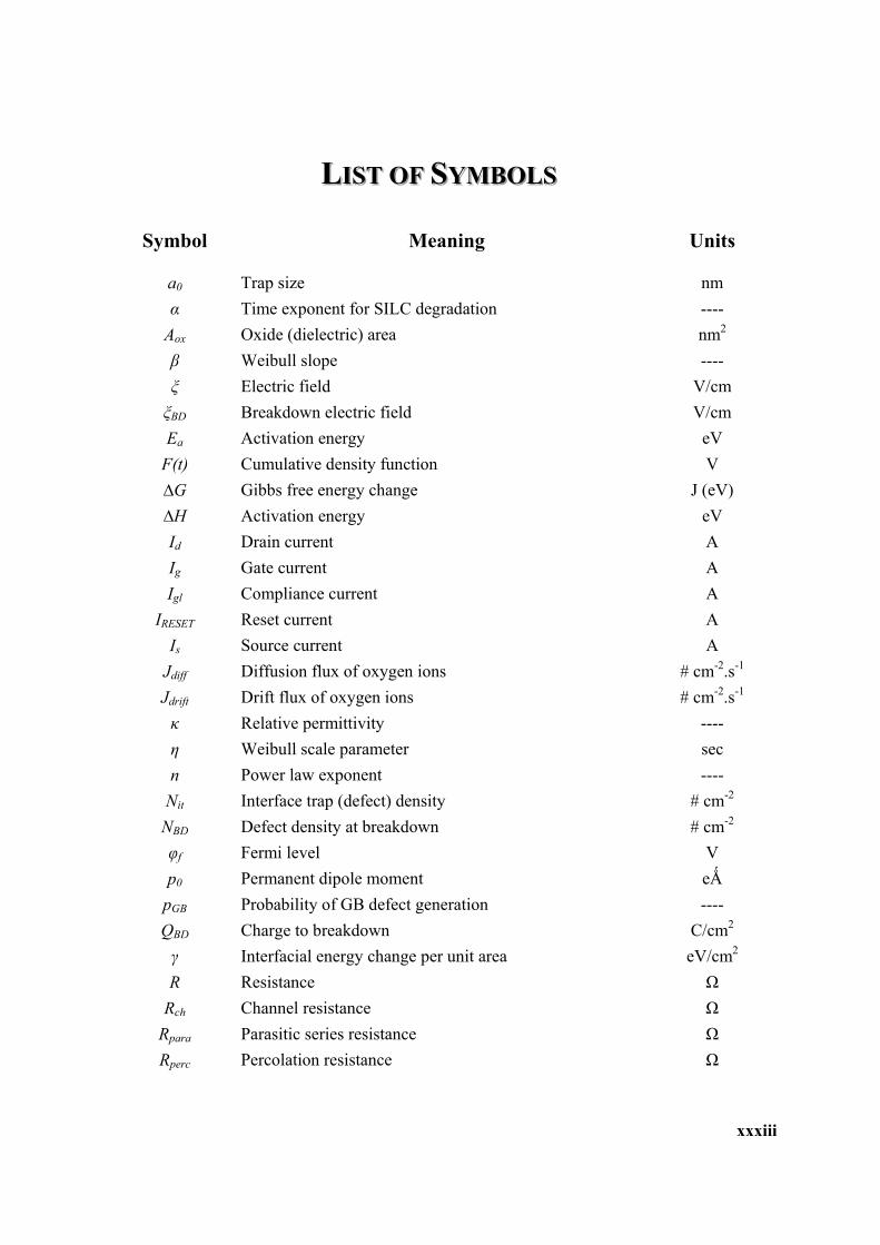
List of Symbols xxxiii
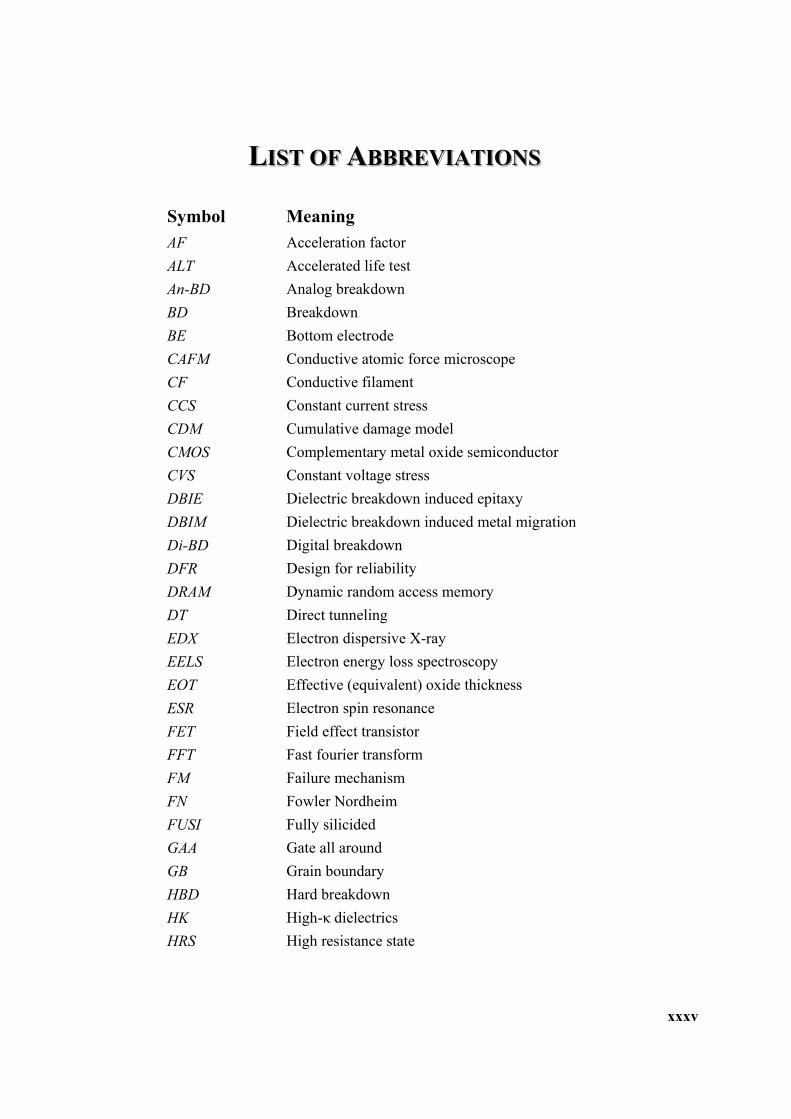
List of Abbreviations xxxv
Chapter One Introduction 1.1 Background 1
1.2 Motivation of Study 7
1.3 Objectives of Study 12
1.4 Organization of Thesis 14
1.5 Specific Contributions 15
Chapter Two Literature Review 2.1 Introduction 17
2.2 High-κ Logic Stack Reliability 18
2.2.1 Fabrication and Process Characterization 18
2.2.1.1 Grain Boundaries in High-κ Films 18
2.2.1.2 Role of the Interfacial Layer 20
2.2.2 Electrical Characterization 21
2.2.2.1 Performance Analysis 21
2.2.2.2 Reliability Analysis 23
A Dielectric Breakdown Field Strength 23
B Time Dependent Dielectric Breakdown 23
C Stress Induced Leakage Current 24
v
D Post Breakdown Phase – Digital Fluctuations 25
E Post Breakdown Phase – Analog Regime 28
F Critical Voltage Governing Oxide Wear-Out 30
G Hard Breakdown 31
H Random Telegraph Noise Effects 31
2.2.3 Reliability Statistics 33
2.2.4 Physical Failure Analysis 37
2.2.4.1 Role of Oxygen Vacancies 37
2.2.4.2 Size of Percolation Path 38
2.2.4.3 Dielectric Breakdown Induced Epitaxy 41
2.2.4.4 Metal Filamentation 42
2.2.4.5 Dielectric Breakdown Induced Metal Migration 42
2.3 Resistive Switching Memory 44
2.3.1 Electrical Characterization 45
2.3.2 Reliability Metrics for Switching Memory 46
2.3.3 Physical Analysis of Switching Mechanism 47
2.4 Summary 48
Chapter Three Electrical Characterization of High-K – Interfacial Layer Breakdown
3.1 Introduction 49
3.2 Experimental Setup 49
3.3 Two-Step Sequential TDDB Algorithm 50
3.3.1 Previous Test Methodologies 50
3.3.2 Proposed Two-Step Sequential TDDB Algorithm 52
3.3.3 Electrical Test Results 53
3.4 Detection of Dual Layer Breakdown Sequence 55
3.4.1 Techniques and Results in the Past 55
3.4.2 Approach A : Poole Frenkel Conduction 57
vi
3.4.3 Electrical Test Results 61
3.4.4 Approach B : 1/f Noise and RTN Study 62
3.4.5 Electrical Test Results 67
3.4.6 Approach C : Critical Breakdown Field Analysis 69
3.4.7 Summary of Breakdown Sequence 73
3.5 Post Breakdown Reliability of Dual Layer Stacks 74
3.5.1 Current Knowhow on Post Breakdown Reliability 74
3.5.2 Application of Critical Voltage for MG-HK Analog BD 75
3.6 Summary 82
Chapter Four Statistical Modeling and Analysis of Dual Layer Dielectric Stacks
4.1 Introduction 83
4.2 Statistical Modeling of Silicon Oxide Breakdown 84
4.3 Limitations of Current Statistical Approaches 86
4.4 Cumulative Damage Model 88
4.4.1 Model Details 88
A Cumulative Distribution Function 89
B Load Sharing System Reliability 91
4.4.2 Statistical Data Analysis 93
A Weibull Slope Analysis 96
B Area Scaling and Circuit Reliability Implications 97
4.4.3 Inferences 100
4.5 New Analytical Percolation Model 102
4.5.1 Earlier Percolation Models 103
4.5.2 Proposed Percolation Model 106
4.5.3 Simulation Results and Discussion 110
4.6 Kinetic Monte Carlo Simulations 113
4.6.1 Motivation and Novelty 113
vii
4.6.2 Chemistry of Trap Generation 114
4.6.3 Kinetic Monte Carlo Routine 115
4.6.4 Simulation Results and Discussion 116
A Zero Interfacial Layer Stack 118
B Dual Layer Dielectric Thin Film Stack 123
4.6.5 Summary 131
4.7 Summary 133
Chapter Five Recovery of Dielectric Breakdown and Correlation to Resistive Switching
5.1 Introduction 134
5.2 Recovery of Hard Breakdown 135
5.3 Recovery of Soft Breakdown 144
5.4 Correlating Breakdown Recovery to Switching 151
5.5 Summary 155
Chapter Six Electrical Characterization to Decipher Resistive Switching Mechanism
6.1 Introduction 156
6.2 Test Structure and Device Details 156
6.3 Polarity and Compliance Dependent Switching 157
6.4 Dual Mode Switching Device 164
6.5 Switching Performance Characterization 166
6.6 Kinetics of Filament Evolution 172
6.7 Interesting Design Applications of our Test Structure 175
A Hybrid Logic Memory Device 176
B Dual Mode Switching Memory 176
C Multi-Bit Storage Device 177
D Ultra-Low Power Switching 177
E RRAM Scalability to Sub-10 nm 179
viii
F Forming Free Operation 179
6.8 Summary 180
Chapter Seven Reliability Metrics for Switching Memory
7.1 Introduction 182
7.2 Retention Lifetime 182
7.2.1 HRS Retention in Oxygen Vacancy Mode 183
7.2.2 LRS Retention in Oxygen Vacancy Mode 187
7.2.3 HRS Retention in Metal Filament Mode 192
7.2.4 LRS Retention in Metal Filament Mode 196
7.3 Endurance Degradation 200
7.4 Read Disturb Immunity 202
7.5 Summary 207
Chapter Eight Conclusion and Recommendations
8.1 Summary of Result Achieved 208
8.1.1 Logic Device Reliability 208
8.1.2 Resistive Switching Memory 210
8.2 Recommendations for Further Work 211
8.2.1 Unresolved Issues for Front-End Device Reliability 211
8.2.2 Further Scope for Resistive Memory Study 215
List of Publications 217
Bibliography 221
ix
AAABBBSSSTTTRRRAAACCCTTT
High-κ (HK) dielectric thin films are currently the most suited insulators for complementary
metal-oxide-semiconductor (CMOS) technology in silicon based sub-32nm nodes enabling
aggressive equivalent oxide thickness scaling and reduction in leakage current due to the
physically thicker film. Hafnium-based dielectrics (HfO2, HfSiON) are widely used in both
advanced logic and memory device structures.
While reliability studies to qualify the metal gate (MG) – HK stacks have been ongoing for
the past few years, there are still many unresolved issues relating to the physical and statistical
nature of the time dependent dielectric breakdown (TDDB) failure mechanism at the front-end.
Some of the critical issues identified include (a) deciphering the sequence of breakdown (BD) in
the dual layer dielectric stack comprising HfO2 and a thin interfacial layer (IL) of SiOx, (b)
studying the origin behind the non-Weibull stochastic nature of BD, (c) decoding the reliability
of the individual HK and IL layers, (d) studying the role played by grain boundary (GB)
microstructural defects on the HK BD statistics, (e) investigating the feasibility of a zero
interfacial layer (ZIL) device for sub-16nm nodes from a reliability point of view and (f)
extrapolating the device level analysis results to circuit level reliability assessment. These issues
form the motivation of the first part of this project focusing on HK-based logic devices. We use a
suite of electrical characterization techniques, statistical modeling and Kinetic Monte Carlo
simulation tools along with failure analysis results as supportive evidence to find solutions to all
the above listed issues.
Our results clearly indicate IL to be the first layer to BD for all values of gate voltage (both
operating and accelerated stress conditions) and combinations of HK and IL film thickness, tHK :
x
tIL. Simulations revealed that localized non-random defect generation due to presence of GB
defects in polycrystalline HK gives rise to the non-Weibull convexial distribution of failure data.
The GB fault lines serve as low activation energy paths for oxygen vacancy (defect) diffusion,
thereby resulting in early time to failure. Based on the detailed statistical analysis and two-stage
sequential TDDB test algorithm developed (which enables us to “arrest” BD after a single layer
percolates and subsequently stress the second layer at lower levels to initiate complete
breakdown of the stack in finite time), we conclude that at the circuit level, leakage failure
criterion (standard criterion being Ig ~ 10µA at Vop = 1V) is attained only due to multiple
uncorrelated IL soft breakdown (SBD) events, rather than a single catastrophic hard breakdown
of the whole stack. Due to the single layer SBD events, leakage current and joule heating through
the percolated regions is still quite low implying that analog wear-out of the BD path is
negligible in HK-IL stacks. Since IL serves as a buffer preventing complete stack percolation,
realization of ZIL devices for sub-16 nm nodes may suffer from lower TDDB lifetime and higher
intrinsic current leakage due to the GB planes with high density of process induced traps
bridging (shorting) the gate and the substrate directly. Interesting observations on the possibility
of material-dependent recovery of dielectric BD have been presented. We demonstrate that it is
possible to initiate “self-repair” of an integrated circuit by simply reversing the stress polarity
that causes the stored oxygen ions in Ni/Ti/Ta-based metal gates to drift back to the percolation
path and passivate the oxygen vacancy (V02+) traps, thereby rejuvenating the transistor
performance substantially.
Based on our electrical observations of post-breakdown recovery in MG-HK M-I-S logic
stacks, we have also been able to explain the origin of resistive switching phenomenon in HfO2-
based M-I-M RRAM, which constitutes the second half of this study. The M-I-S transistor has
xi
been successfully used as a potential ultra-thin oxide high quality test structure for switching
studies, in order to understand the kinetics of multiple filament nucleation, degree of correlation
in filament locations (during different SET events) and the role of the anode / cathode terminals
in our asymmetric electrode gate stack.
Using electrical tests for unipolar and bipolar ramp sweep, we have identified two distinct
compliance-dependent (Igl) switching mechanisms governed by oxygen ion transport (Igl ~ 1µA)
and metallic nano-filaments (Igl ~ 100µA-1mA) respectively. These two mechanisms are entirely
independent. While the V0 mode of switching is only bipolar and observed for any oxygen
gettering electrode (e.g., Ni, Ti, Ta), the MF mode is non-polar and observed only for Ni
filaments due to their low melting point and tendency to “spike” through the dielectric during
filament formation with very small size ~ 2 nm (implying high surface area – to – volume ratio)
that further reduces the critical temperature for filament rupture. The reset transition is drift
driven for V0 mode, while for the MF mode, current density - joule heating assisted filament
dissolution is the driving force. Statistical thermodynamic models have been applied in order to
quantitatively estimate the retention reliability of the memory stack at the low and high
resistance states for both these mechanisms of switching. Towards the end, we propose the
interesting possibility of dual mode switching operation of an RRAM using a single gate stack
and realization of hybrid logic-memory integration at the front-end given that the M-I-S logic
stack is able to function as a resistive switching device under certain conditions of voltage
application. In order to increase memory storage density, the transistor structure can be used for
2-bit data storage by forcing filaments to nucleate at the two corner regions of the device and
operating the source and drain terminals independently.
xii
The novelty of our study lies in the ability to separate the TDDB failure in the HK and IL
layers using our new test algorithm with precisely controlled compliance and stress voltages that
enables us to “arrest” BD of the dual layer stack at a stage when only one of the dielectrics has
broken down and then subsequently apply a lower stress to cause the second layer to eventually
percolate. Most of our electrical and statistical analysis is based on the successful
implementation of this two-stage TDDB accelerated test. This is one of the first reports that
document a solid approach to BD controllability in dual layer dielectric films. The inferences and
conclusions in this work are based on a synergy of electrical, statistical, simulation models and
physical analysis results.
xiii
LLLIIISSSTTT OOOFFF FFFIIIGGGUUURRREEESSS
Figure Page
1.1 Technology roadmap of Intel® showing the electrical oxide thickness and gate leakage trends for poly-Si – SiON technology and its transition to MG-HK stacks for sub-65 nm nodes [24].
4
1.2 Trend of current density (j) versus equivalent oxide thickness (EOT)
showing the trend and electrical data for SiO2 → SiON → high-κ (HfSiON / HfON) [25]. The reduction in nominal current density by two-three orders of magnitude can be clearly seen.
4
1.3 Illustration showing the trap generation scenario at the breakdown
(percolation) stage for very thin and thick oxides. The critical trap density prior to BD in ultra-thin oxides is very low implying the oxide does not suffer much damage even though TDDB occurs. However, the trap density for thick oxides is very high at the percolation stage [37] (i.e. oxide already suffers sufficient wear-out) and therefore, at the instant of percolation, the BD is destructive and “hard” with no progressive BD reliability margin. The typical Ig-t trends for the two different cases are also included. Yellow circles represent the “traps” and the dark arrow marks represent the progressive lateral wear-out of the percolated region from SBD eventually to HBD in the thin oxides.
6
1.4 (a) Conventional SiO2 / SiON based MOSFET device with gate material
that was poly-silicon or fully silicided Ni (FUSI). (b) With the advent of high-κ technology, we have a dual layer dielectric stack comprising of a very thin parasitic SiOx interfacial layer (typically 5-12Ǻ) and a physically thick HK dielectric such as HfO2 / HfSiON. Though the physical thickness of the HK stack is larger, the EOT value ≡(κSiO / κHK)× tHK is aggressively scaled down by a factor of ~ 4-6. The gate electrode for HK stacks is generally metal-based TiN or TaN, so as to avoid Fermi-level pinning and poly-Si depletion effects.
8
1.5 (a) Schematic showing the amorphous microstructure with very few
process induced traps during HK deposition followed by the standard annealing process which causes the HK to evolve into a (b) polycrystalline columnar microstructure with grain boundary lines. Even the defects existing in the bulk tend to migrate (as indicated by the arrows) and segregate towards the GB [57] (which acts as a sink for vacancies) as governed by the thermodynamics of lowering the system free energy. These GB lines therefore function as “weakest link” and given their low activation energy for vacancy diffusion, it is also possible for the vacancies to preferentially accumulate at the HK-IL interface.
10
xiv
Also, notice the increase in the IL layer thickness due to the annealing process.
2.1 Outline of topics to be reviewed for the high-κ logic stacks (Section 2.2)
as well as resistive switching memory, RRAM (Section 2.3) in the order of fabrication → electrical characterization → reliability study → physical analysis. Note that the fabrication process for the logic and memory study is the same as we are using the M-I-S stack as the structure to understand resistive switching mechanism.
18
2.2 Analyzing the nano-resolution conduction map of a 5 nm polycrystalline
HfO2 thin film using conductive atomic force microscopy [75]. The image on the left is the topography showing depressions at certain regions of the deposited film. The image on the right shows bright white spots corresponding to high leakage which correlate well with the depressions in the topography image, which are the grain boundary contours.
19
2.3 TEM micrograph of a ZrO2 deposited film on Si substrate wherein the (a)
initial as-deposited IL layer thickness is very thin, which becomes very thick (b) after annealing at 7000C due to substantial IL layer growth (bright contrast region in the image) [54]. Also, it is worth noting that the high-κ becomes increasingly polycrystalline with smaller grain sizes during the annealing process.
20
2.4 (a) Extracted mobility trends for a poly-Si gated HfO2 and SiON stack
showing the significant mobility degradation in high-κ dielectric based devices due to remote coulomb and phonon scattering [91]. (b) Achieving a zero-IL device by use of a good oxygen gettering electrode such as Ti. The oxygen scavenging effect is illustrated in the inset [64].
22
2.5 (a) Trend of variation in the dielectric breakdown strength with the
permittivity of the material [93]. The solid line is the trend of variation which closely matches with theoretical predictions of an inverse square root law. (b) Typical trends of TDDB in a dual layer HfO2-SiOx gate stack at various stress conditions [94].
23
2.6 Trend of leakage current evolution with time in a HfO2-based stack with
an initial duration of charge trapping in the process induced traps that causes current to decrease and reach a minimum. When charge trapping saturates, the TAT current induced by additional trap generation starts to dominate and the leakage current henceforth increases. The figure on the right is the obtained by extracting the charge trapping component out of the test data in the left figure [94].
25
2.7 (a) Schematic showing the physics governing the random telegraph noise
(RTN) behavior that arises due to capture / emission of carriers (electrons) 27
xv
in the oxygen vacancy traps after breakdown [106]. The electrical test data shown correspond to RTN trends in (b) post-BD 4.2 nm SiO2 [107], (c) post-BD HfSiO-SiON (EOT ~ 1.2 nm) [108] and (d) pre-BD SILC stage in SiON (0.7 nm) – HfO2 (1.8 nm) [109]. In (d), it is worth noting that a 4-level fluctuation in Ig is observed corresponding to the presence of 2 active traps.
2.8 (a) Post-BD gate current evolution in 22Ǻ SiON showing two distinct
trends – an initial duration of digital fluctuations followed by an analog monotonous increase in current due to wear-out [101]. (b) Schematic showing the “discrete” change in conduction values which arises due to different ON-OFF combinations of the traps in the percolation path. (c) Analog stage of wear-out may be attributed to the lateral dilation of the percolation path or the nucleation of microstructural defects (black shaded region in the figure) that cause effective oxide thinning. (d) Typical post-TDDB (with compliance Igl = 1µA) Ig-Vg trends (Vg < Vcrit ~ 2.6-3.0V) in the digital BD stage [101] where leakage can be significantly low(e.g. at time instants of 1000 and 2000 sec) when most of the traps are “OFF” / “inactive”. (e) Ig-Vg trends in the analog BD stage (Vg > Vcrit ~ 3.2-3.4V) for the same device shows leakage current values 3-4 orders larger than the fresh device [101].
29
2.9 Typical trends of (a) Id-Vg and (b) Id-Vd degradation ranging from fresh
device to post-TDDB digital stage (2µA) and subsequent analog BD stages of 30µA and 60µA in a 16Ǻ poly-Si gated SiON device. While MOS performance trends may be acceptable and functional at SBD digital stage (2µA), it degrades significantly by 30-40% in the analog stage and as shown for the (c) case of HBD [101], functionality is completely lost. The analog stage may not even exist for metal gated devices implying that the digital phase is followed immediately by a catastrophic HBD event.
30
2.10 An overall picture of dielectric breakdown evolution in the sequence of
SILC → TDDB → Di-BD → An-BD → HBD stages. Every stage corresponds to a unique trap configuration and conduction behavior of the oxide. As will be discussed later, the analog progressive BD stage is only valid for poly-Si gated devices. As for metal gated stacks, the digital fluctuation stage is directly followed by a catastrophic HBD due to the vulnerability of the metal gate to migrate and punch through the degraded oxide assisted by the high localized temperature, current density and joule heating conditions.
32
2.11 (a) Extrapolation of accelerated stress data shows the orders of magnitude
difference in the lifetime estimate at low voltage conditions when applying the three different models – 1/ξ, ξ and power law [127]. (b) Experimental I-V data shows a change in the transport tunneling mechanism from direct tunneling (DT) to Fowler-Nordheim tunneling (F-
36
xvi
N) at low and high voltages respectively [127]. A change in tunneling mechanism can imply a change in the failure kinetics when the trap generation is fluence driven, rather than field-driven. (c) TDDB data for SiO2 plotted on a Lognormal scale show a concave trend with large deflections from linearity at very low and very high percentile values [130]. Therefore, lognormal distribution is not suitable to represent dielectric breakdown. The Weibull plot however shows good linearity. (d) Failure data in the HK-IL stack when plotted on a Weibull scale always shows some non-linearity, with a steeper distribution (Weibull slope) at low percentile values [134]. This is due to non-random trap generation and presence of dual-layer material dielectric “system”.
2.12 (a) Technique used to perform physical analysis using TEM/EELS. The
location of BD is detected electrically using the weighted ratio of the drain and source currents. Elemental composition analysis at the BD location is carried out “relative” to an unbroken oxide region as the reference [135]. (b) The EELS O K-edge count data in red show a significant drop in oxygen content at the BD location [136]. (c) Gaussian oxygen deficiency profile for different BD compliances [116]. It is clear that harder BD contains a wider and higher peak oxygen vacancy distribution and laterally dilating percolation path. (d) Trend of the peak percolation core sub-stoichiometric ratio, x, in the digital and analog regimes for SiOx [123]. For very hard BD, we observe x → 0 implying formation of a pure-Si nanowire at the core of the BD region.
39
2.13 TEM micrographs of the various failure defects observed in different gate
stacks → (a) Si nanowire (nano-cluster) in the hard BD stage at the core of the percolation path, (b) DBIE Si epitaxial defect which results in effective oxide thinning, (c) Ni spiking (migration) into the Si substrate punching through the oxide, (d) Ta isotropic migration forming a bowl-shaped defect signature, (e) NiSi encroachment from the S/D contacts and (f) illustration showing the diffusive nature of Ni which causes it to encroach into the channel region. In the extreme case, the diffused Ni from both the source and drain contacts may merge and cause a channel short. Reference for (a) – (d) is [123] and for (e, f), [143].
40
2.14 (a) Schematic of the simple RRAM structure which is an M-I-M capacitor
stack. I-V trends illustrating the (b) unipolar and (c) bipolar modes of switching [159].
45
3.1 (a) Picture of the probe tips landing on the bond pads of the tested
transistor. (b) The SUSS 8-inch probe station used for all our electrical tests. The system at the bottom is the thermal chuck heater with a range of 25-2000C. (c) SCS-4200 semiconductor parameter analyzer with two pre-amplifiers for measurement of high resolution and very low currents up to the femto-ampere range.
50
xvii
3.2 Flow chart of the proposed two-stage CVS TDDB methodology that
involves two discrete separate stages of stressing each with a different stress voltage (Vg) and compliance setting (Igl). After the first layer BD is “arrested”, the device performance trends (Ig-Vg, Id-Vg and Id-Vd) are measured prior to the next stage of stressing. The measured Ig-Vg trend is compared with the Poole-Frenkel conduction mechanism to detect the layer which breaks down first.
52
3.3 Two stage time-dependent SILC-TDDB trends in a poly-Si – HfO2 – SiOx
– Si stack, using the proposed algorithm in Fig. 3.2. The circle and square symbols represent the first and second layers to break down respectively.
53
3.4 Typical Ig-Vg trends in the HK-IL stack for fresh device, 1-layer BD, 2-
layer BD and progressive BD (high compliance setting of 100µA). There is a clear change in leakage by a few orders of magnitude for every successive stage of BD.
54
3.5 Schematic showing the trapping and detrapping process of electron charge
carriers at trap potential wells. The potential barrier is reduced by the applied electric field and carrier transport is thermally enhanced in this Poole-Frenkel conduction process, which is typical of high-κ dielectric thin films [187].
58
3.6 Arrhenius plot of temperature dependence tests for the Poole-Frenkel
mechanism aimed at determining the “effective” trap depth for a fresh HK-IL device. Oxygen vacancy traps in HK dielectrics have a shallow trap depth of ФB ~ 0.48eV.
59
3.7 Band diagram schematic assuming IL BD, illustrating the existence of
Poole-Frenkel conduction only for Vg >1V, when the shallow traps (ФB ~ 0.48eV) in the intact HfO2 layer align with the Si conduction band. For Vg < 1V, only direct tunneling conduction is possible. The value of Vg ~ 1V is quantitatively determined by Band Diagram simulations [193].
60
3.8 Poole-Frenkel plot of Ig-Vg data after one-layer BD in six of the tested
devices at Vg > 1V. From the slope of the least square fitting, it can be deduced whether HK or IL is the first layer to breakdown.
61
3.9 Schematics showing the four possible scenarios of a HK-IL bi-layer stack
device operation – (A) fresh device, (B) HK-only BD, (C) IL-only BD and (D) complete HK+IL stack BD. White and black circles represent process and stress induced immobile traps (oxygen vacancies) respectively. Arrows illustrate possible TAT sites for electron tunneling transport. Initially, a trap with no electron capture is considered “active” as it can assist in TAT conduction. When injected electrons from substrate
64
xviii
get captured in the V02+ trap, it becomes “inactive” and shuts-off
continuity of percolation path. The RTN signals observed are basically various combinations of “active” and “inactive” traps at any time instant that govern the values of Ig and ∆I.
3.10 (a, b) Schematic showing the discrete two-step current fluctuations and
the corresponding 1/f2 Lorentzian spectrum due to capture / emission events from a single trap. (c) As the number of traps increases, the superposition of several 1/f2 spectra tends towards a combined 1/f1 trend. As a rule of thumb, it can be stated that for about 5 traps or more, the observed signal is almost 1/f1 type.
65
3.11 Dependence of the trap / detrap time constant on the tunneling distance
into the dual layer dielectric stack based on the WKB approximation, assuming an elastic tunneling model.
65
3.12 Low voltage gate current random telegraph signal for (a) fresh device
where discrete fluctuations represent the number of process induced traps, (b) after 1-layer BD and (c) after 2-layer BD. There is a big change of many orders of magnitude in the RTN current step (∆I) for these three different stages. All devices tested have dimensions of W × L = 0.5 × 0.5µm2.
66
3.13 Power spectral density (PSD) plot of gate current RTN signals measured
on many similar devices for (a) fresh device (Vg = 1.5V, Ig-RTN ~ 2-5 pA, W = (0.5, 5)µm, L = 0.5µm) (b) after 1-layer TDDB (Vg = 1V → Ig-RTN ~ 2 nA; Vg = 1.5V → Ig-RTN ~ 70 nA) and (c) after 2-layer TDDB (Vg = 1.5V → Ig-RTN ~ 3µA). Note the wide variation in the magnitude of the PSD as well as exponent, α. Area of devices tested range from (0.03 - 2.50) µm2.
69
3.14 Thermochemical model prediction of the breakdown strength, ξBD, as a
function of the dielectric constant, κ. The trend clearly shows an inverse square root dependence.
70
3.15 (a) Two-stage sequential TDDB trends (same as Fig. 3.3) observed in
three NMOS devices of the HK-IL gate stack where BD is arrested at the one-layer BD stage using stringent compliance control setting. (b) Weibull plot of the gate voltage stress applied for the first and second stage TDDB test in the proposed two-stage CVS algorithm.
71
3.16 HRTEM image of the poly-Si HfO2-SiOx gate stack showing the HK
thickness, tHK = 44Å and IL layer thickness, tIL = 8-12Å [207]. 72
3.17 (a) Post breakdown gate current evolution in a 16Ǻ poly-Si SiON gate
stack at Vg = 2.6V showing the evolution of the digital fluctuations into the analog regime. (b) Random telegraph noise (RTN) fluctuations in the
76
xix
post-BD stage for SiON at relatively low voltages of Vg = 1.5, 1.8 and 2.1V where BD is achieved by a TDDB constant voltage stress with a low compliance capping of Igl ~ 1µA, corresponding to soft breakdown.
3.18 Experimental trend of the statistical spread of Vcrit for five different SiON
gate stacks with tox ranging from 12 - 22Ǻ [101]. A large sample size of about 15-50 devices were tested for each oxide thickness. The value of Vcrit saturates at 2V for tox < 14Ǻ. If the saturation were not observed, then Vcrit ~ Vop, which would imply very low post-BD reliability margin for ultra-thin dielectrics.
77
3.19 (a) to (e) - RTN fluctuations in the HK-IL stack after one-layer IL BD.
For all Vg up to 3V, we only observe digital leakage, as the voltage drop across the percolated IL is only about 35%·Vg < Vcrit. For Vg ~ 3V, the remaining HK layer is prone to TDDB and no analog evolution of BD in the IL layer is observed at this stage. The presence of a dual layer stack prevents evolution of the percolated IL region (after one-layer BD) into the analog regime.
78
3.20 Trends of (a) transfer curve Id-Vg in a poly-Si-HfO2-SiOx stack and (b)
drive current trend, Id-Vd in a NiSi-HfSiON-SiOx FUSI stack for fresh device, IL first layer BD and subsequent complete stack BD. Note that the electrical trends are acceptable for one-layer BD but far from ideal for the case of (IL + HK) breakdown. This is more so the case for NiSi stack considering the migration of gate material into the oxide that causes complete malfunction of the transistor.
79
3.21 (a) to (f) - RTN fluctuations in the HK-IL stack after dual-layer TDDB
shown for Vg ranging from 2.50-3.25V. For Vg ≤ 3V, digital signals are clearly observed. At Vg = 3V, we observe a sudden current spike, following which, 1/f noise signals corresponding to the analog BD regime are detected.
80
3.22 (a) and (b) Evolution of the gate voltage for constant current stress (CCS)
of Ig ~ 4µA and 30µA. The red dotted line indicates the maximum value of Vcrit for tox ~ 16Ǻ. The gate voltage is much larger than the maximum Vcrit (by 0.2-0.6V) for a prolonged duration in both cases. (c) Post-CCS RTN signal at Vg = 1.5V shows clear digital fluctuation trends for the case of current capped at 4µA. (d) However, the RTN signal for capping of 30µA exhibits 1/f noise trends. This implies that evolution of digital to analog BD is governed not just by the stress voltage, but also by the compliance current. For very low compliance capping (Igl < 5µA), there is insufficient driving force for substantial DBIE epitaxial growth.
81
4.1 Illustration showing the (a) vertical upward shift of the Weibit line for
device to circuit level extrapolation and the (b) lateral rightward shift of 85
xx
the line for scaling from accelerated stress to operating voltage conditions. This is the standard extrapolation methodology used conventionally for SiO2 and SiON.
4.2 Application of a single stage CVS with high compliance setting in various
HK-IL dual layer stack TDDB studies. It is generally difficult to observe a clear two-step BD trend. Only if the surviving layer after the first layer BD has a high critical field strength (or large physical thickness) can two-step BD trends be observed as in (a, c) [96, 172, 226, 227].
86
4.3 Use of single stage ramp voltage stress (RVS) for HK-IL gate stacks.
Again, there is no clear distinct observation of two-step BD here as the second surviving layer shows abrupt instantaneous percolation [172, 228].
87
4.4 (a) Illustration of the time varying voltage step stress profile across each
layer of the dielectric stack. (b) Reliability block diagram for the HK-IL system. (c) Cumulative failure plot of the surviving HK layer showing the scaling of the first layer TDDB failure time to an equivalent time corresponding to a higher level stress of VHK ~ Vox2.
89
4.5 Statistical bimodal Weibull plot for IL and HK layers extrapolated to
operating voltage condition of Vg = 1V using the inverse power law (IPL) acceleration model.
93
4.6 System reliability plot for the “load sharing” HK-IL dual layer stack
obtained using the model proposed in Eqns. (4.12)-(4.14). The convexity of the line at low Weibit clearly suggests that overall HK-IL stack BD is “non-Weibull”.
94
4.7 Comparison of the load-sharing HK-IL dependent system model with the
HBD data after bi-layer BD at Vg = 3.5V. The close match of the test data and model imply that the model well describes HK-IL failure statistics. Inset shows some of the HBD single stage CVS leakage evolution trends in the bi-layer stack.
95
4.8 Use of the inverse power law model for lifetime extrapolation of the HK
and IL layers shows that both have similar power law exponents, but HK is always far more reliable than the IL. Circuit failure is more likely to be due to multiple IL BD events rather than a single IL → HK complete stack BD.
97
4.9 (a) Trends of Ig-Vg leakage after one-layer IL BD in various devices. At
Vop = 1V, the leakage can widely range anywhere between 0.1-10 nA. (b) Theoretical calculation of the low percentile lifetime enhancement (χ) achieved due to multiple uncorrelated IL SBD events using Weibull approximation for βIL = 0.821, assuming a monomodal distribution. The
99
xxi
value of χ is found to saturate for K > 50 BD events. This saturation is a typical characteristic of multiple BD events [233].
4.10 Schematic showing the evolution of multiple IL BD spots at the circuit
level wherein the sum of the RTN fluctuations from these percolated traps add up to reach circuit compliance. The dark bold lines in the HK represent the columnar microstructure grain boundary (GB) fault lines and the grey circles represent the localized process induced traps at these GB sites.
100
4.11 Schematic showing the three different possible scenarios of electric field
drop across the HK and IL layers [44]. Depending on the ratio of HK to IL thickness, tHK : tIL, the stress voltage applied determines whether the electric field in any of the two layers exceeds its BD field value. For a true intrinsic reliability study, it is necessary to stress the device in region 1 where both layers are experiencing a stress level lower than their respective BD fields. This schematic is only for illustration purpose and it is based on the assumed value of κ = 25 for HfO2 and κ = 3.9 for SiOx.
102
4.12 Typical percolation cell diagram illustrating a random trap configuration
and a particular combination of these traps forming a “non-columnar” percolation path. The colored cells represent the lateral limit of extension of any percolation path evolving from a particular bottom cell marked “”. A robust percolation model has to account for all possibilities of percolation path formation – both columnar and non-columnar.
104
4.13 (a) Schematic of a cell-based 2D matrix for high-κ dielectric with a trap
size of a0 and lateral mean grain size of d0. The colored columns represent the GB and the grey shaded cells are the region of influence around GB where percolation process could involve interaction of nearest neighbor (NN) bulk and GB traps (as illustrated by the “X” labeled active traps that could constitute one configuration of the percolation path). (b) Evolution of the trap density with time before the critical trap density (NBD) is reached can be approximated by the standard power law expression. (c) Probability of trap generation, p(t), is represented by the Poisson distribution that captures the saturating trend of the probability. Factors ξ and α are used to model the probability for bulk and GB trap formation. Existence of active PIT is accounted for by laterally shifting the p(t) along t-axis by t0 where p(t0) = PIT/(N*n), time-zero trap density.
108
4.14 Weibit plots of proposed analytical percolation model showing the effect
of (a) GB, G and G-GB interactions, (b) NN cells around GB, (c) uniform versus non-uniform TGR and columnar versus non-columnar percolation model, (d) device dimension, (e) trap generation rate (ξGB : ξG), (f) SILC exponent (αGB, αG) and (g) oxide thickness (tox/a0). The plot in (h) is the fit of the model to TDDB data for HK-only HfO2 -BD (tox = 44Å).
112 113
xxii
4.15 Flowchart showing the detailed step-by-step procedure of the Kinetic
Monte Carlo (KMC) simulation routine for HK-IL trap generation. The proposed algorithm helps identify the sequence of BD and time to BD of the individual HK and IL layers along with their corresponding BD locations as well. The symbol “rand” here refers to the random number generator with a uniform distribution from (0,1). Note that every simulation trial for each oxide layer involves two independent random numbers, one for choosing the cell to be classified as the new defect and the other one to update the system time clock.
117
4.16 Schematic showing the 2D percolation cell model we have developed for
the dual layer gate stack. Based on experimental evidence of the GB size, we consider the GB (purple cells) to be distributed at regular intervals (with spacing “d”) in the oxide (to keep it simple). This is equivalent to having a random distribution of GB lines for a large area device under test. The parameter, a0, is the trap size (cell dimension). L is the total length of sample (equivalent to area in a 3D case) and NHK and NIL represent the number of layers of HK and IL in the stack. The grey and red cells represent the process and stress induced traps in the oxide respectively.
118
4.17 Simulated failure time distribution for (a) amorphous (κ = 25) and (b)
polycrystalline (κG = 25, κGB = 26) HK thin film of thickness, tHK = 32Å. Higher localized trap generation rate at the GB causes the distribution to be non-Weibull.
119
4.18 Histogram plot of the BD location in the HK film (tHK = 32Å) for different
trap generation rate ratio of GB to bulk degradation – (a) 1:1 (amorphous), (b) 4:1 and (c) 60:1. As expected, BD occurs preferentially at GB locations as the ratio increases by a factor of 10.
120
4.19 Failure distribution plot of the HK film (tHK = 32Å) for different
probability of process induced traps in the GB → pGB = 5%, 15% and 25%. For high pGB, extrinsic low percentile tails are observed.
120
4.20 Trend of Weibull slope (β) versus oxide thickness (tox) for amorphous and
polycrystalline HK dielectric films. A non-zero y-intercept is observed in both cases, with the amorphous HK having a higher intercept.
121
4.21 Hypothetical scenarios that could explain the non-zero positive y-intercept
for β - tox relationship in Fig. 4.20. The additional trap needed could be (a) interface related, (b) due to inclined non-vertical GB fault lines or (c) misalignment of traps.
122
4.22 Simulated TTF distribution for poly-HfO2 film with tHK = 32Å at Vop = 1V 123
xxiii
for four different device area of L = 100, 200, 2000 and 20,000 cells. Area scaling is only valid for large device areas corresponding to L > 2000. Although not show here, for amorphous films, area scaling is always valid for all cases. The inset shows a plot of the Weibull slope (β) increasing for larger area devices. It is expected to saturate for larger device areas, which we did not simulate due to prolonged computational time.
4.23 (a) Trap generation rate in the HfO2 and SiOx layers for different IL layer
thickness (tIL = 4, 8, 16Å) and fixed HK thickness (tHK = 32Å). (b) Trap generation rate in the HfO2 and SiOx layers for different HK layer thickness (tHK = 8, 16, 24Å) and fixed ultra-thin IL thickness (tIL = 4Å). The black and red line plots correspond to HK and IL respectively.
124
4.24 Plot of the ratio of time to first HK and IL break down in a dual layer gate
stack comprising 32Å HfO2 and 16Å SiOx for a wide range of gate voltage stress conditions (each 300 simulation trials). It is clear that lifetime of the HK layer is many orders of magnitude larger than that of the IL layer.
125
4.25 Weibull plot of simulated time to failure for a HK-IL dual layer gate stack
at Vg = 2V, comprising 32Å HfO2 and 16Å SiOx. The figure on the left is for the IL first BD, while the figure on the right is for the HK BD. Data in red and black correspond to polycrystalline and amorphous HK films.
126
4.26 Histogram plot of the first layer (IL) break down location for the
amorphous and polycrystalline HK based dual layer gate stack with tHK = 32Å and tIL = 16Å. First layer BD in the amorphous stack is fully random as expected. As for the poly film, it is mostly confined to the regions below the GB fault lines in the HK.
127
4.27 Statistical distribution of the multiple breakdown spots (up to 10 BD
events) in the IL layer simulated using the proposed thermochemical KMC model. The distributions are non-Weibull and the Weibull slope increases for higher number of BD events, as justified previously in Ref. [234].
128
4.28 (a) Time to failure distribution for first layer IL BD shows validity of area
scaling rule. (b) The scatter plot of HK and IL breakdown location generally shows perfect correlation, which implies that area scaling is not applicable to the second layer HK BD.
130
4.29 Scatter plot of IL and HK breakdown locations as a function of the GB
defectivity. With higher density of process induced traps, it is possible for the HK BD location to be completely uncorrelated to the percolation in the IL.
130
xxiv
4.30 Plot of the β – tox relationship for different values of tHK and tIL in the dual layer gate stack. While βIL shows a linear relationship with tIL, there is no dependence of βHK on tHK because BD is only controlled by the IL layer.
131
4.31 Percolation map illustrating a typical scenario of trap generation in a HK-
IL stack and the correlated IL → HK BD spot at the location L ~ 188. 131
5.1 (a) - Unipolar dielectric breakdown recovery trends at the HBD stage in
NiSi, TiN and TaN gated Hf-based ultra-thin HK gate stacks. Only NiSi-based stack shows significant recovery. (b) Bipolar recovery trends of dielectric breakdown at the HBD stage in NiSi, TiN and TaN gated Hf-based dielectric stacks. Similar to (a), only the FUSI stack shows considerable recovery. The symmetry of recovery trends in unipolar and bipolar cases imply that HBD recovery is only a current-density (joule heating) driven polarity independent phenomenon with filament dissolution taking place at a critical temperature (TCRIT).
136
5.2 (a) Ni and O EELS line profiles in a NiSi gated NMOS at the dielectric
failure site. With reference to the non-failure site (ideal region with no breakdown effect taken as reference for comparison), the BD region shows O diffusion towards the gate and Ni diffusion into the substrate. (b) TEM micrograph showing the migration and “spiking” of Ni from the gate preferentially along the [111] direction. The inset is the high angle annular dark field (HAADF) version showing the spike as a bright slanted line [146].
137
5.3 HAADF micrograph showing the migration of Ta (bright region of bowl-
shaped protrusion) through the dielectric into the substrate from the TaN gate NMOS after hard breakdown [62].
138
5.4 Repeated observations of partial and full recovery of gate leakage current
during Ig-Vg sweep after a 100µA compliance controlled HBD in the FUSI-HfSiON(25Ǻ)-SiOx(12Ǻ) sample. Partial recovery involves leakage drop by 2-3 orders of magnitude, while full recovery corresponds to 5-7 orders leakage reduction such that the recovered current is almost as good as the fresh device leakage value.
139
5.5 (a) Simple resistive circuit model for HK-IL breakdown with the various
resistive regions (components) labeled. (b) Weibull plot of extrapolated data at channel and corner BD regions at Vg = 1V for post recovery TDDB accelerated life test analysis. (c) High resolution TEM micrograph [123] showing the migration of Ni from the drain contact towards the corner of the active channel region by the DBIM mechanism causing new NiSix (x > 2) phase formation.
140
5.6 (a) Electrical test data scatter plot of recovery voltage (VREC) with the 142
xxv
HBD filament location (sBD). Red line is the quadratic line of best fit which follows the trend described by Eqns. (5.1) and (5.2). (b) Ig-Vg trends showing the dependence of VREC on the breakdown hardness and percolation resistance (Rperc), controlled by tuning the compliance, Igl. No “unipolar” recovery is observed for very low Igl of 0.7µA, where only one layer BD has occurred.
5.7 Illustrating the SET (a, c) and RESET (b, d) transitions for a single HBD
filament at channel (a, b) and corner (c, d) regions. Better switching is expected for corner filaments due to low resistivity NiSix phase formation at the S/D extension region that induces an MIM-like stack and enhances the thermal confinement.
143
5.8 High resolution TEM micrograph of post BD TaN gated device for BD
hardness capped at Igl = 2µA and 8µA [62]. Clear evidence of Ta filamentation can be observed in the high angle annular dark field (HAADF) inset only for the case of Igl = 8µA. As for SBD (Igl < 5µA), filament nucleation does not take place and the percolated region only comprises oxygen vacancies.
145
5.9 Ig-Vg plots for (a) poly-Si (0.25µm2), (b) NiSi (0.12µm2), (c) TiN (90nm
× 100nm) and (d) TaN (90nm × 100nm) gated Hf-based dielectric stacks for SBD with different compliance settings corresponding to a wide range of BD hardness. The solid lines correspond to the case of SBD, while the dotted lines represent the leakage conduction measured after negative Ig-Vg sweep induced recovery (see Fig 5.10(a)). The dash-dotted grey line is the initial leakage current prior to stress testing.
146
5.10 Recovery in Ig-Vg observed during the negative voltage ramp stress sweep
after SBD at compliance of 1 – 5µA. A sequence of RESET in the leakage current is observed instead of a single abrupt switching, observed typically in the case of HBD filament rupture. (b) Trend of IREC/I0 with BD hardness (Igl) for the TiN-HfLaO gate stack. The value of IREC/I0 is measured at Vg = 1.0, 1.5 and 2.0V and indicates the extent to which Ig after recovery approaches the fresh device leakage. (c) Box plot showing the trend of post-recovery BD voltage versus Igl. (d) Statistical Weibull plot of voltage at which recovery is initiated (VREC) and the subsequent VBD.
148
6.1 Trends of RESET in the oxygen vacancy governed regime (low
compliance) for the following cases : (a) and (d) are unipolar modes with positive and negative TE voltage, respectively. (b) and (c) are bipolar modes with VSET > 0V and VSET < 0V, respectively. Significant switching is only observed for bipolar mode in (b) due to the high oxygen solubility of the metal-based TE, while the silicon BE does not function as an oxygen reservoir.
158
xxvi
6.2 TEM micrographs of devices after forming stage with compliance capped
at (a) Igl = 5µA and (b) Igl = 100µA respectively [146]. It is clear that metal filaments nucleate only for Igl >> 5µA.
159
6.3 Ellingham diagram showing the standard Gibbs free energy of oxidation
for different transition metal elements and silicon. The trends here relate to the oxygen affinity of different metal gates (used as TE) relative to that of the silicon substrate (BE) [274].
160
6.4 Trends of RESET in the metallic filament regime (high compliance) for
the following cases : (a) and (d) are unipolar modes with positive and negative TE voltage respectively. (b) and (c) are bipolar modes with VSET > 0V and VSET < 0V respectively. Interestingly, significant switching is observed for all four cases.
161
6.5 (a) and (b) Switching mechanism in the V0 regime is dependent on the
drift and diffusion forces as well as oxygen solubility of the electrode towards which oxygen ions drift during SET. O2- ions that move towards the Si BE tend to get oxidized (Si-O). (c) and (d) Switching mechanism in MF regime involves Ni rupture where source of Ni can be from gate (TE) or S/D contact. Oxygen ions only play a secondary role in this regime. The length of the arrows in (a) and (c) indicate the strength of drift / diffusion driving forces.
162
6.6 Endurance trend with 100 cycles of switching wherein the first 50 cycles
represent V0 mode and the second 50 cycles represent the MF mode. The current immediately before (ILRS) and after (IHRS) RESET are shown in this plot.
164
6.7 Proposed methodology of operation of the Ni-gated RRAM device
wherein resistive switching is initiated in the V0 mode. After degradation of the memory window, we intentionally transit to the MF mode that results in an increased switching window and prolonged endurance.
165
6.8 Trend of (a) memory window (log scale) and (b) VRESET for a wide range
of SET Igl values. We observe good consistent switching (~100% of devices tested) with low VRESET and large window only for very low and very high Igl. As for the intermediate Igl range, only 46% of devices show very minor switching.
166
6.9 Logarithmic I-V plot of LRS state for (a) Igl ~ 0.7µA and (b) Igl ~ 0.7mA
respectively. Exponent n >> 1 for low Igl implies TAT conduction, while n ~ 1 for high Igl suggests ohmic (resistive) behavior, observed in metallic filaments.
167
xxvii
6.10 Weibull probability plot of (a) IRESET and (b) memory window, log(ILRS/IHRS), comparing the RESET current and order of switching for the V0 and MF regimes. The arrows in part (a) represent the significant reduction in RESET current (power) for the V0 mode, relative to the MF mode.
168
6.11 Weibull probability plot of SET and RESET voltage in the V0 and MF
modes. The MF mode has a wider voltage switching margin; however the spread of RESET voltage in MF mode is also very high. Note that all the voltage data plotted above are the absolute values, i.e. although VRESET < 0V for bipolar switching in V0 mode, we only plot its modulus value, |VRESET| here.
168
6.12 Retention test at VREAD = 0.5-1.0V and T = 85-1500C for the V0 and MF
modes. Both modes show very good retention lifetime with minimal influence of any RTN-induced fluctuations.
170
6.13 Variation of the conductive filament (BD) location along the M-I-S
transistor structure channel for ~50 and ~10 cycles of switching in the (a) MF and (b) V0 modes respectively. Clusters of data for the sFIL location in MF mode imply “pseudo-random” and “correlated” nature of filament nucleation. As for the V0 mode, filament nucleation is purely “random” and “uncorrelated”.
174
6.14 Illustration showing the (a) increased efficiency in passivation of oxygen
vacancy traps for higher bipolar VRESET in the V0 mode and (b) the partial and fully ruptured filaments in the MF mode which cause the “pseudo-random” nature of filamentation process. In the case of a partially ruptured metal filament, the electric-field across the ruptured region during the next SET cycle is sufficiently high such that it becomes favorable for the ruptured filament to nucleate again. This is more so the case if the ruptured filament is sharply pointed due to the lightning rod effect [294].
175
6.15 Operation scheme for the transistor-based RRAM so as to achieve two-bit
memory realization by independently controlling the filamentation process at the (a) source and (b) drain terminals with non-zero Vd and Vs respectively. The truth table shows the various possible combinations of binary data storage in this multi-bit configuration depending on the breakdown state of the drain and source corner regions.
178
6.16 Illustration showing the trap configuration and percolation map of the
dielectric after SET at low compliance for (a) dual layer film and (b) single layer film. The intact dielectric in the dual-layer case helps reduce the RESET current, thereby enabling realization of ultra-low power switching device. It may be better to use two different dielectric materials
179
xxviii
for the dual layer film for easier BD confinement.
6.17 Possibility of multiple stages of RESET in the MF mode suggest the possibility of existence of multiple filaments in the 0.15µm2 area devices tested. However, aggressive scaling of the device to 10 nm × 10 nm may lead us into single filament based switching operation.
181
7.1 (a) Schematic showing the approach used to find the location of CF along
transistor channel in inversion regime. The grey and hashed regions represent HfSiON and SiOx respectively. The brown shaded region is the CF location in the SiOx layer. (b) Uncorrelated variation in sFIL for 9 switching cycles clearly shows the random nature of CF nucleation and rupture. Note here that we use a very low compliance of 1-2µA in order to confine the BD event and operate in the V0 mode.
184
7.2 (a) Scatter plot of VSET for N=50 cycles confirms the random uncorrelated
filamentation phenomenon (forming stage data not shown). (b) Probability plot of VSET for RR = 12 and 80 mV/s showing adherence to Weibull stochastics.
185
7.3 (a) Extrapolated retention time (TRET) for a wide range of VREAD using the
inverse power law model and (b) maximum VREAD for different area devices considering the threshold 10 year retention criterion.
185
7.4 Simple schematic showing the hypothetical scenario of uncorrelated V0
trap generation and passivation in a dielectric resulting in different CF for two arbitrary consecutive cycles where (A→B; C→D) transitions refer to SET while (B→C) refers to RESET. The grey cells represent the traps remaining prior to the Kth SET event. The blue and green cells correspond to new stress induced traps during Kth and (K+1)th SET respectively. The dotted lines denote the contour of the percolation path or CF. Note the passivation of many traps during the RESET (B→C). The trap configuration prior to every SET transition is random and different, as can be seen comparing A and C.
187
7.5 (a) Two-stage process involved in RESET which includes O2- ionic
transport across the HK layer all the way to the HK-IL interface and subsequent trap passivation reaction with the vacancies residing in the percolated IL region. (b) Chemical potential gradient of O2- ions which results in a diffusive force which may counteract or superimpose the voltage-induced drift force depending on the polarity and magnitude of VTE.
188
7.6 (a) Probability distribution of bipolar VRESET for 100 cycles of RESET
transition. (b) Calculated oxygen ion drift velocity for different assumed activation energy barriers. (c) Minimum read voltage for retention
189
xxix
immortality in the LRS state. (d) I-V trends showing a clear memory window surpassing current fluctuations only for VTE > 0.6V.
7.7 (a) Probability plot of VSET for the MF mode at three different voltage
sweep ramp rates. No dependence of VSET on the ramp rate is observed. (b) Scatter plot showing the change in VSET for about 50 cycles of consecutive switching in an M-I-S device (forming stage data not shown). Clear trends of reducing VSET are observed confirming the accumulative damage suffered by the dielectric during multiple switching cycles in the MF mode.
193
7.8 (a) Trend of free energy change versus filament radii during
inhomogeneous MF phase nucleation. There is a critical energy barrier that has to be overcome for filament nucleation and growth to be favorable and spontaneous. (b) Illustration showing the small Ni metal fragments in the dielectric which can coalesce to form a MF if V > VTH.(c) Illustration showing the initial shape of a formed filament, which laterally expands at the two ends, while “necking” down at the centre, prior to the RESET event which causes MF to rupture.
194
7.9 (a) Probability plot of VRESET for two different ramp rates (RR) showing a
direct correlation between the two quantities. (b) Resistance evolution with slowly ramped Vg in the LRS state of the MF mode, up to the instant of sudden filament rupture. The complete rupture process can be split into three different stages.
195
7.10 Finite element simulation of the (a) temperature and (b) thermal gradient
profile in a Ni filament using the resistive heating module of the COMSOL® Multiphysics package. The peak temperature is in the central part of the filament, while the thermal gradient is the highest at the top and bottom side-interfaces. We assume the filament-dielectric interfaces to be ideal thermal insulators, while the filament-electrode interfaces to be perfect heat sinks implying T ~ 300K at the electrode.
197
7.11 Simulated variation of filament temperature (TFIL) for VREAD = 0.05 –
0.15V with (a) time at the central core of the filament and (b) distance along vertical-axis of filament. The temperature at any point of the filament reaches a steady state after finite time. (c) Maximum temperature point in the filament for a few low values of VREAD and (d) Melting point of a Ni nanowire as a function of its radius, estimated from Ref. [262].
198
7.12 Endurance trends for the (a) V0 and (b) MF modes plotted for 30-50
switching cycles. In the MF mode, the device failed after 50 cycles. Note that in part (a), we plotted the endurance trends in terms of the leakage current at HRS and LRS, while in part (b), we show the calculated resistance value in the two states. Either the resistance or the current value
201
xxx
can be used to represent the conduction state.
7.13 Evolution of the conductivity fluctuations (Ig) with time for (a) fresh device, (b) device at LRS after SET, (c) device at HRS after RESET and (d) subsequent SET transition, all in the V0 mode. The fluctuations in all the cases is well within an order of magnitude even for the high VREAD. Also, notice the RTN noise (1/f2) Lorentzian signal for the device at LRS due to stochastic charge trapping / detrapping.
202
7.14 Power spectral density plot of current fluctuations in the four cases
corresponding to the results shown in Fig. 7.13. The power-law fitted slope in the low frequency range for these signals provides information on source of noise (1/f, thermal, RTN). Of these, the RTN noise shows highest ∆I/I.
203
7.15 Simple illustration showing the band diagram of the oxide in the LRS for
low and high VREAD values. Only at higher VREAD, is the band bending of the oxide sufficient such that the shallow traps in the high-κ layer are accessible to the tunneling charge carriers from the bottom electrode (substrate) conduction band. Therefore, for higher VREAD, noise is dominated by RTN resulting in high ∆I/I (though still within an order of magnitude) and ILRS >> IHRS due to the trap-assisted transport.
204
7.16 Evolution of the conductivity fluctuations (Ig) with time for (a) fresh
device, (b) device at LRS after SET and device at HRS after RESET for the case of (c) partial and (d) full MF rupture.
204
7.17 Power spectral density plot of current fluctuations in the four cases
corresponding to the results shown in Fig. 7.16. Full filament rupture (corresponding to 4-5 orders of switching) is associated with 1/f noise, while partial rupture (2-3 orders of switching) results in the Lorentzian 1/f2 spectrum.
205
7.18 I-V trends of the switching device in the LRS and HRS states for the (a)
MF and (b) V0 modes. Clear difference in conduction state is observed even for very low VREAD in the MF mode.
206
8.1 Illustration of a 2 nm polycrystalline HfO2 film deposited by (a) single
stage of ALD and (b) two stages of ALD each with 1 nm film thickness. The GB misalignment for the two-layer HK film with the same effective thickness results in improved robustness to TDDB as more traps are needed to initiate a percolation path. The green and red traps refer to process and stress induced ones respectively.
214
xxxi
LLLIIISSSTTT OOOFFF TTTAAABBBLLLEEESSS
Table Page
2.1 Summary of the failure defects observed in various gate material – SiON / high-κ stacks and their driving forces.
43
3.1 Summary of the testing methodologies and results from various
research groups on the first layer to BD in a dual-layer HK-IL gate stack.
56
4.1 Statistical distribution parameters of the high-κ (HfO2) and interfacial
(SiOx) layers determined using maximum likelihood estimation (MLE) of the CDM model based distribution function.
94
4.2 Magnitude of the various factors affecting the Weibull slope for the
early and wear-out failure mechanisms (FM) in the HK and IL layers. 96
4.3 Possible permutations of bulk and GB traps originating from the NN
grain cells and GB cells. 109
4.4 Values for the various parameters of the thermochemical bond
breaking model extracted from literature reports based on atomistic / experimental studies.
116
5.1 Material properties, oxygen solubility and recovery trends observed in
the four different gate electrode material based high-κ stacks. 147
5.2 Comparison of the conventional terminologies used for dielectric
breakdown and RRAM and the similarities and differences in their standard test structure.
153
6.1 Trends of switching in the Ni-gated stack for various polarity
combinations of VSET and VRESET (unipolar and bipolar) at low and high current compliance for forming / SET transition.
157
6.2 Switching trends in the V0 and MF regimes for different stress
polarities of SET and RESET. The terms “yes” refers to good switching window, while “no” refers to non-existent switching.
163
6.3 Physical mechanism and driving forces for resistive state transition in
RRAM. 169
6.4 Holistic comparison of the various RRAM performance and reliability
metrics in the V0 and MF modes of operation. Endurance in MF mode 171
xxxii
is lower due to the destructive nature and difficulty in controlling breakdown hardness during filament nucleation. The green cells represent favorable trends.
6.5 Comparison of the RESET current and switching power of our MIS dual-layer RRAM device with other low power switching device reports in the literature.
178
xxxiii
LLLIIISSSTTT OOOFFF SSSYYYMMMBBBOOOLLLSSS
Symbol Meaning Units
a0 Trap size nm α Time exponent for SILC degradation ----
Aox Oxide (dielectric) area nm2
β Weibull slope ---- ξ Electric field V/cm ξBD Breakdown electric field V/cm Ea Activation energy eV
F(t) Cumulative density function V ∆G Gibbs free energy change J (eV) ∆H Activation energy eV Id Drain current A Ig Gate current A Igl Compliance current A
IRESET Reset current A Is Source current A
Jdiff Diffusion flux of oxygen ions # cm-2.s-1 Jdrift Drift flux of oxygen ions # cm-2.s-1
κ Relative permittivity ---- η Weibull scale parameter sec n Power law exponent ----
Nit Interface trap (defect) density # cm-2
NBD Defect density at breakdown # cm-2 φf Fermi level V p0 Permanent dipole moment eǺ
pGB Probability of GB defect generation ---- QBD Charge to breakdown C/cm2
γ Interfacial energy change per unit area eV/cm2
R Resistance Ω Rch Channel resistance Ω
Rpara Parasitic series resistance Ω Rperc Percolation resistance Ω
xxxiv
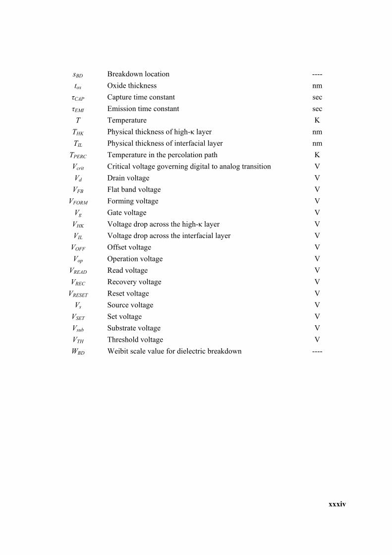
sBD Breakdown location ---- tox Oxide thickness nm τCAP Capture time constant sec τEMI Emission time constant sec T Temperature K
THK Physical thickness of high-κ layer nm TIL Physical thickness of interfacial layer nm
TPERC Temperature in the percolation path K Vcrit Critical voltage governing digital to analog transition V Vd Drain voltage V VFB Flat band voltage V
VFORM Forming voltage V Vg Gate voltage V
VHK Voltage drop across the high-κ layer V VIL Voltage drop across the interfacial layer V
VOFF Offset voltage V Vop Operation voltage V
VREAD Read voltage V VREC Recovery voltage V
VRESET Reset voltage V Vs Source voltage V
VSET Set voltage V Vsub Substrate voltage V VTH Threshold voltage V WBD Weibit scale value for dielectric breakdown ----
xxxv
LLLIIISSSTTT OOOFFF AAABBBBBBRRREEEVVVIIIAAATTTIIIOOONNNSSS
Symbol Meaning
AF Acceleration factor ALT Accelerated life test An-BD Analog breakdown BD Breakdown BE Bottom electrode CAFM Conductive atomic force microscope CF Conductive filament CCS Constant current stress CDM Cumulative damage model CMOS Complementary metal oxide semiconductor CVS Constant voltage stress DBIE Dielectric breakdown induced epitaxy DBIM Dielectric breakdown induced metal migration Di-BD Digital breakdown DFR Design for reliability DRAM Dynamic random access memory DT Direct tunneling EDX Electron dispersive X-ray EELS Electron energy loss spectroscopy EOT Effective (equivalent) oxide thickness ESR Electron spin resonance FET Field effect transistor FFT Fast fourier transform FM Failure mechanism FN Fowler Nordheim FUSI Fully silicided GAA Gate all around GB Grain boundary HBD Hard breakdown HK High-κ dielectrics HRS High resistance state
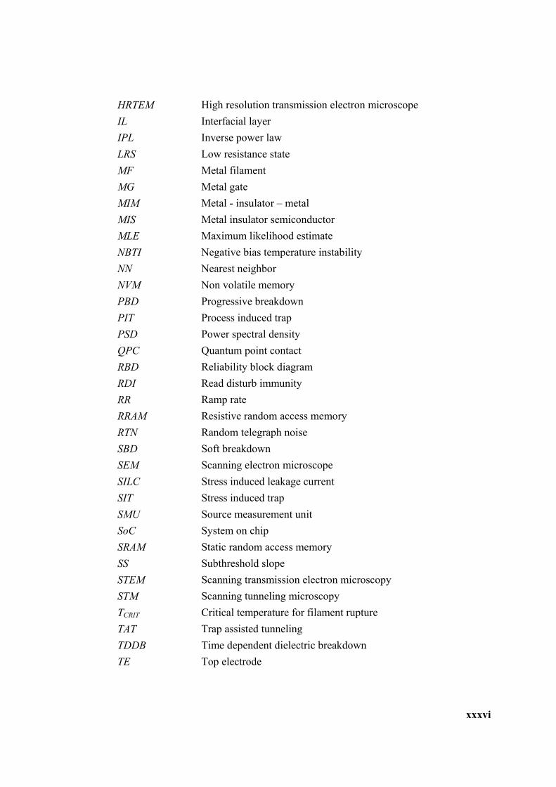
xxxvi
HRTEM High resolution transmission electron microscope IL Interfacial layer IPL Inverse power law LRS Low resistance state MF Metal filament MG Metal gate MIM Metal - insulator – metal MIS Metal insulator semiconductor MLE Maximum likelihood estimate NBTI Negative bias temperature instability NN Nearest neighbor NVM Non volatile memory PBD Progressive breakdown PIT Process induced trap PSD Power spectral density QPC Quantum point contact RBD Reliability block diagram RDI Read disturb immunity RR Ramp rate RRAM Resistive random access memory RTN Random telegraph noise SBD Soft breakdown SEM Scanning electron microscope SILC Stress induced leakage current SIT Stress induced trap SMU Source measurement unit SoC System on chip SRAM Static random access memory SS Subthreshold slope STEM Scanning transmission electron microscopy STM Scanning tunneling microscopy TCRIT Critical temperature for filament rupture TAT Trap assisted tunneling TDDB Time dependent dielectric breakdown TE Top electrode
xxxvii
TEM Transmission electron microscopy TGR Trap generation rate TTF Time to failure ULSI Ultra large scale integrated WKB Wentzel-Kramers-Brillouin approximation ZIL Zero interfacial layer
CHAPTER ONE
1
CHAPTER ONE
IIINNNTTTRRROOODDDUUUCCCTTTIIIOOONNN
1.1 BACKGROUND
Over the past 4-5 decades, semiconductor technology has undergone tremendous
development starting from the vacuum tubes in the 1960s to the nanoelectronic devices
comprising the complementary metal-oxide-semiconductor (CMOS) technology era that we
operate in today, wherein the metal-oxide-semiconductor field effect transistor (MOSFET) is the
fundamental building block of the integrated circuit. We have been continuously downscaling
the size of the transistor in accordance to the famous empirical Moore’s Law [1-3] from a
channel length of L = 1µm in the 1990s to as low as L = 28-32 nm in 2011. Current research
activities in the industry have been directed towards 16 nm, 11 nm and even sub-10 nm
technology nodes for the near future [4, 5]. This drastic reduction in transistor size is
accompanied by an increase in the integration density of these devices to realize ultra large scale
integrated (ULSI) circuits which form the backbone of our modern electronic gadgets with
higher speed (frequency response), smaller size (portability) and enhanced functionality. With
every evolving generation in the miniaturization of nanoscale transistors, existing intrinsic failure
mechanisms tend to get more severe with higher rate of degradation and additionally, it is also
possible for new failure mechanisms to crop up in the quantum regime, given the higher electric
field, leakage current, power dissipation and thermal stress factors that accompany the scaling
down of technology. Another issue concerning scaling is the increased variability in the device
fabrication process which results in increased spread of the output electrical performance metrics
CHAPTER ONE
2
[6, 7] as well as the time to device / circuit failure. This variability could also go to extent of
inducing new extrinsic failure modes in the integrated circuit, if not controlled by robust design
techniques [8, 9]. Considering all these factors, it is clear that a comprehensive reliability and
physics of failure study is required for nanoscale devices and circuits at every new technology
node prior to qualification for commercial high-end large scale integrated system fabrication.
Reliability and failure studies for nanoelectronic devices and circuits can be classified as (A)
front-end, back-end and package-level and from another perspective as (B) device and circuit-
level. Conventional failure mechanisms at the front-end [10] include gate oxide (high-κ dielectric)
time-dependent dielectric breakdown (TDDB) [11], negative bias temperature instability (NBTI)
[12], hot carrier injection (HCI) [13] and electrostatic discharge (ESD) [14]. At the back-end, the
key issues are electromigration (EM) [15], stress migration (SM) [16], interaction of EM and SM
in narrow line interconnects [17] and low-κ dielectric TDDB [18]. At the package-level which
serves as an interface between the chip and the outside world, solder EM, corrosion, mechanical
and thermal fatigue and wire bond delamination are some of the key concerns [19].
The focus of this doctoral study is on the front-end failure mechanism of time-dependent
dielectric breakdown (TDDB) and post breakdown (post-BD) in high-κ gate dielectric stacks.
SiO2 / SiON (referred to as oxynitride) has been the conventional oxide material used in MOS
technology since its inception. Over the past decades until about 2004, SiO2 / SiON showed
excellent insulative property with the oxide thickness (tox) ranging above 3-4 nm [20]. This
native oxide (growing from the Si substrate) was very compatible with the silicon-based process
flow (containing very few process induced traps / defects in the bulk) and the interface between
the Si-SiO2 layer was of high quality with a very low interfacial trap (defect) density (Nit ~ 108 -
1010 eV-1cm-2) [21]. However, with aggressive downscaling, as the oxide thickness was also
CHAPTER ONE
3
reduced, the advanced technology nodes since 2007 required oxynitride thicknesses as low as 0.8
– 1.2 nm, which corresponds to only 2-3 monolayers of Si-O atoms. For such ultra-thin oxide
layers, the leakage current density (which increases exponentially with reduction in oxide
thickness) tends to be very high > 10-1000A/cm2 [22], way beyond the acceptable limits which
could lead to high power dissipation and Joule heating during operation of the integrated circuit.
Moreover, such thin insulators with very few atomic layers may tend to lose their intrinsic
insulative property itself. Therefore, continued use of the SiON leads us to a fundamental
roadblock to achieving further scaling. To overcome this limitation, high-κ (HK) dielectric thin
film materials such as HfO2, HfSiON and ZrO2 were explored [22, 23]. For a physically thicker
HK film, it is possible to achieve the same or improved coupling capacitance of the gate to the
inversion channel with a much lower equivalent oxide thickness (EOT) due to the significantly
higher permittivity (κ) of these HK materials (which could range from κ ~ 12-30 as compared to
SiON with κ ~ 6). This is explained by Eqn. (1.1) below where the capacitance density, C = κox /
tox. The nominal leakage current after transition from SiON → HK material technology reduced
by 2-3 orders of magnitude, simply due to the increase in the physical thickness of the HK film,
as illustrated by the Intel® Technology Roadmap [24] in Fig. 1.1 and the current density – EOT
plot in Fig. 1.2 [25].
SiONHKSiONSiON
HKHK
SiON
SiON
HK
HK
;tt
ttC
εεεε
εε
>>⋅=
==
(1.1)
Dielectric breakdown is a vastly studied topic over the past few decades for various
applications [26]. The breakdown phenomenon in a wide range of oxide materials including
ceramics [27] have been investigated in the past. It is believed that breakdown occurs by the
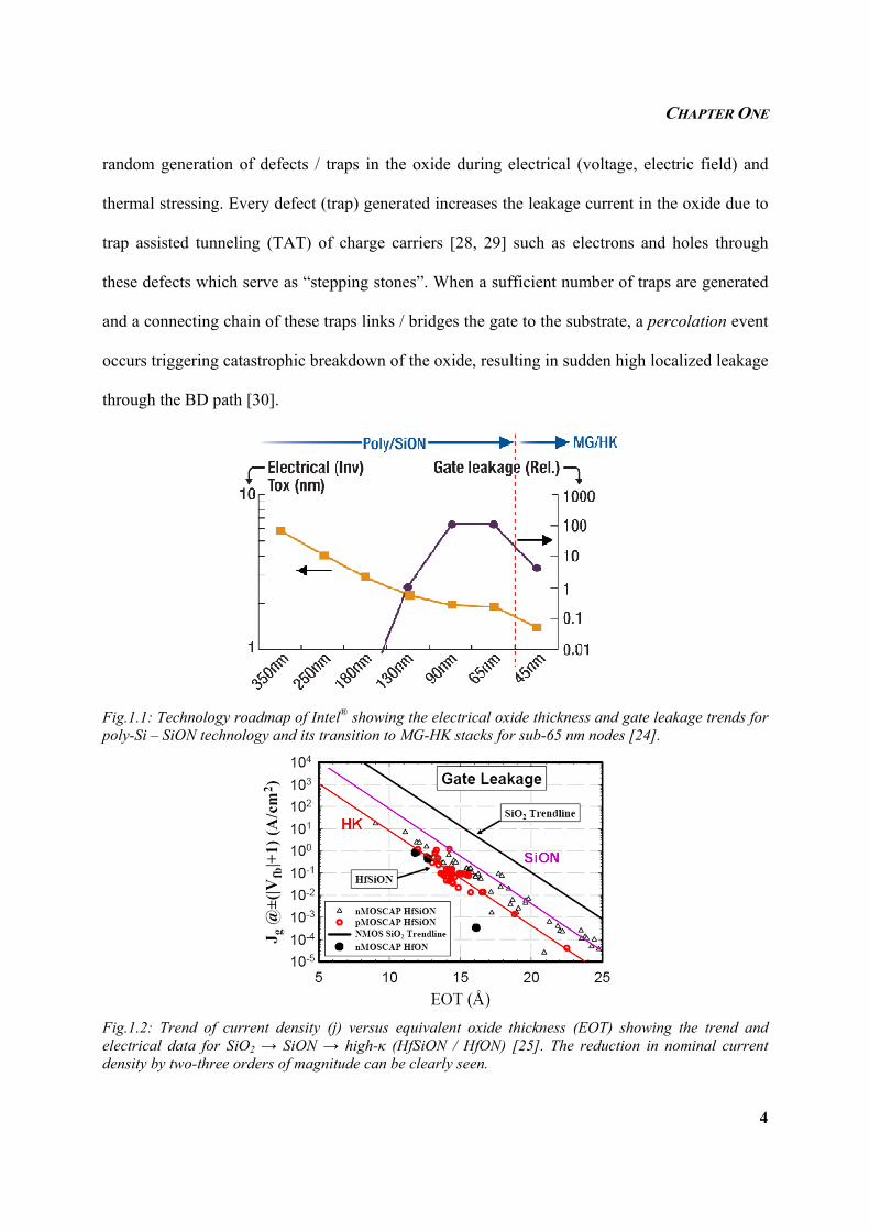
CHAPTER ONE
4
random generation of defects / traps in the oxide during electrical (voltage, electric field) and
thermal stressing. Every defect (trap) generated increases the leakage current in the oxide due to
trap assisted tunneling (TAT) of charge carriers [28, 29] such as electrons and holes through
these defects which serve as “stepping stones”. When a sufficient number of traps are generated
and a connecting chain of these traps links / bridges the gate to the substrate, a percolation event
occurs triggering catastrophic breakdown of the oxide, resulting in sudden high localized leakage
through the BD path [30].
Fig.1.1: Technology roadmap of Intel® showing the electrical oxide thickness and gate leakage trends for poly-Si – SiON technology and its transition to MG-HK stacks for sub-65 nm nodes [24].
Fig.1.2: Trend of current density (j) versus equivalent oxide thickness (EOT) showing the trend and electrical data for SiO2 → SiON → high-κ (HfSiON / HfON) [25]. The reduction in nominal current density by two-three orders of magnitude can be clearly seen.
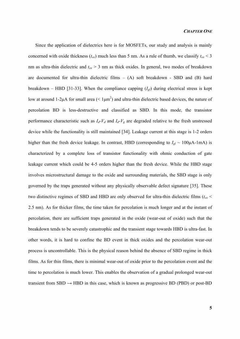
CHAPTER ONE
5
Since the application of dielectrics here is for MOSFETs, our study and analysis is mainly
concerned with oxide thickness (tox) much less than 5 nm. As a rule of thumb, we classify tox < 3
nm as ultra-thin dielectric and tox > 3 nm as thick oxides. In general, two modes of breakdown
are documented for ultra-thin dielectric films – (A) soft breakdown - SBD and (B) hard
breakdown – HBD [31-33]. When the compliance capping (Igl) during electrical stress is kept
low at around 1-2µA for small area (< 1µm2) and ultra-thin dielectric based devices, the nature of
percolation BD is less-destructive and classified as SBD. In this mode, the transistor
performance characteristic such as Id-Vd and Id-Vg are degraded relative to the fresh unstressed
device while the functionality is still maintained [34]. Leakage current at this stage is 1-2 orders
higher than the fresh device leakage. In contrast, HBD (corresponding to Igl ~ 100µA-1mA) is
characterized by a complete loss of transistor functionality with ohmic conduction of gate
leakage current which could be 4-5 orders higher than the fresh device. While the HBD stage
involves microstructural damage to the oxide and surrounding materials, the SBD stage is only
governed by the traps generated without any physically observable defect signature [35]. These
two distinctive regimes of SBD and HBD are only observed for ultra-thin dielectric films (tox <
2.5 nm). As for thicker films, the time taken for percolation is much longer and at the instant of
percolation, there are sufficient traps generated in the oxide (wear-out of oxide) such that the
breakdown tends to be severely catastrophic and the transient stage towards HBD is ultra-fast. In
other words, it is hard to confine the BD event in thick oxides and the percolation wear-out
process is uncontrollable. This is the physical reason behind the absence of SBD regime in thick
films. As for thin films, there is minimal wear-out of oxide prior to the percolation event and the
time to percolation is much lower. This enables the observation of a gradual prolonged wear-out
transient from SBD → HBD in this case, which is known as progressive BD (PBD) or post-BD
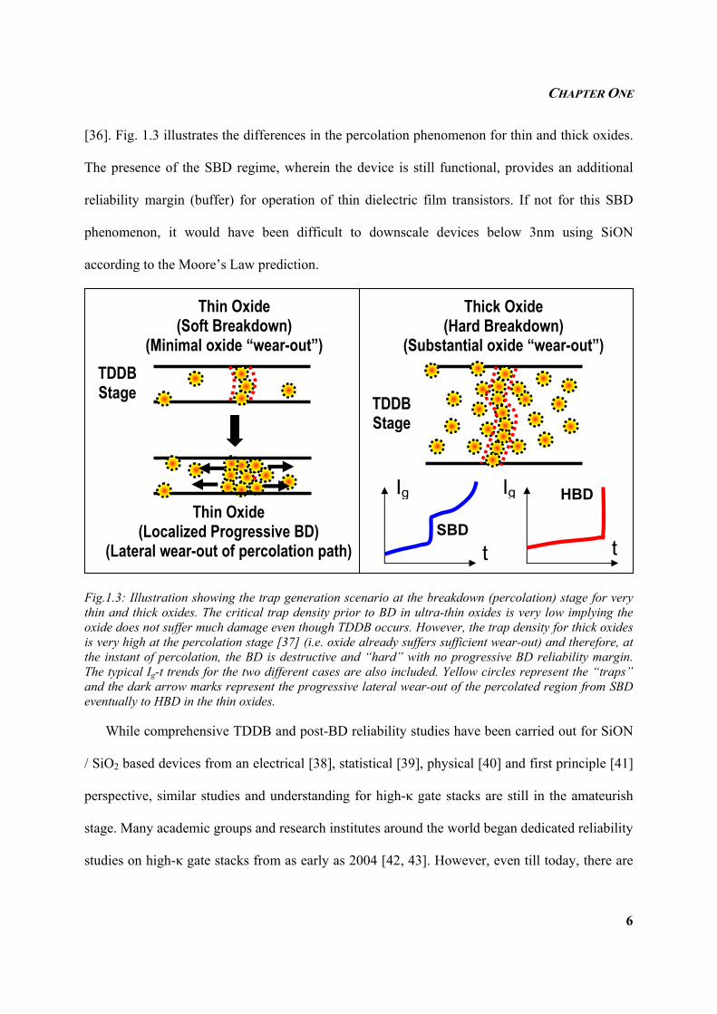
CHAPTER ONE
6
[36]. Fig. 1.3 illustrates the differences in the percolation phenomenon for thin and thick oxides.
The presence of the SBD regime, wherein the device is still functional, provides an additional
reliability margin (buffer) for operation of thin dielectric film transistors. If not for this SBD
phenomenon, it would have been difficult to downscale devices below 3nm using SiON
according to the Moore’s Law prediction.
Fig.1.3: Illustration showing the trap generation scenario at the breakdown (percolation) stage for very thin and thick oxides. The critical trap density prior to BD in ultra-thin oxides is very low implying the oxide does not suffer much damage even though TDDB occurs. However, the trap density for thick oxides is very high at the percolation stage [37] (i.e. oxide already suffers sufficient wear-out) and therefore, at the instant of percolation, the BD is destructive and “hard” with no progressive BD reliability margin. The typical Ig-t trends for the two different cases are also included. Yellow circles represent the “traps” and the dark arrow marks represent the progressive lateral wear-out of the percolated region from SBD eventually to HBD in the thin oxides.
While comprehensive TDDB and post-BD reliability studies have been carried out for SiON
/ SiO2 based devices from an electrical [38], statistical [39], physical [40] and first principle [41]
perspective, similar studies and understanding for high-κ gate stacks are still in the amateurish
stage. Many academic groups and research institutes around the world began dedicated reliability
studies on high-κ gate stacks from as early as 2004 [42, 43]. However, even till today, there are
Thin Oxide (Soft Breakdown)
(Minimal oxide “wear-out”)
Thick Oxide (Hard Breakdown)
(Substantial oxide “wear-out”)
Thin Oxide (Localized Progressive BD)
(Lateral wear-out of percolation path)
TDDB Stage
TDDB Stage
SBD
HBDIg
t
Ig
t
CHAPTER ONE
7
many results that tend to be unsubstantiated, unclear and phenomenological in this domain and a
good understanding of the physical and statistical nature of high-κ BD is still lacking [44]. Hence,
we decided to address this need at this right time by focusing on the statistical and electrical
characterization of high-κ stacks and correlating them with the physical microscopic evidence of
defect chemistry that other members of our research group here are concurrently investigating.
The need for an in-depth high-κ reliability study is also spurred by the use of these transition
metal oxides (TMO) such as HfO2 and ZrO2 in current and future non-volatile memory (NVM)
devices such as flash memory [45] and resistive random access memory (RRAM) [46]. Given
that the metal-insulator-semiconductor (MIS) stack for logic devices is similar to the metal-
insulator-metal (MIM) stack in RRAM except for the substitution of the silicon substrate by a
metal electrode and the SIS/MIS stack is used for flash memory architecture, the insight into
kinetics of degradation and physics of failure in logic transistors will in turn help understand
phenomenon (mechanism) of charge trapping in Flash memory [47] and resistive switching in
RRAM during the forming / SET stage [48] which corresponds to a transition from the high to
low resistance state (HRS → LRS) in the memory device upon application of sufficiently high
voltage. Our aim is to only understand the switching mechanism in RRAM using the results of
high-κ breakdown. We shall not be dealing with the charge trapping in Flash memories as there
are other reports which have already addressed these in sufficient detail [47].
1.2 MOTIVATION OF STUDY
There are various factors which make the reliability study of high-κ dielectric thin films more
complicated than it would appear. While the study of oxynitride BD involved a single oxide
material (SiON) sandwiched between the gate and the substrate and “grown” using the Si
substrate as the template, in the case of high-κ stacks, an external deposition source using either a
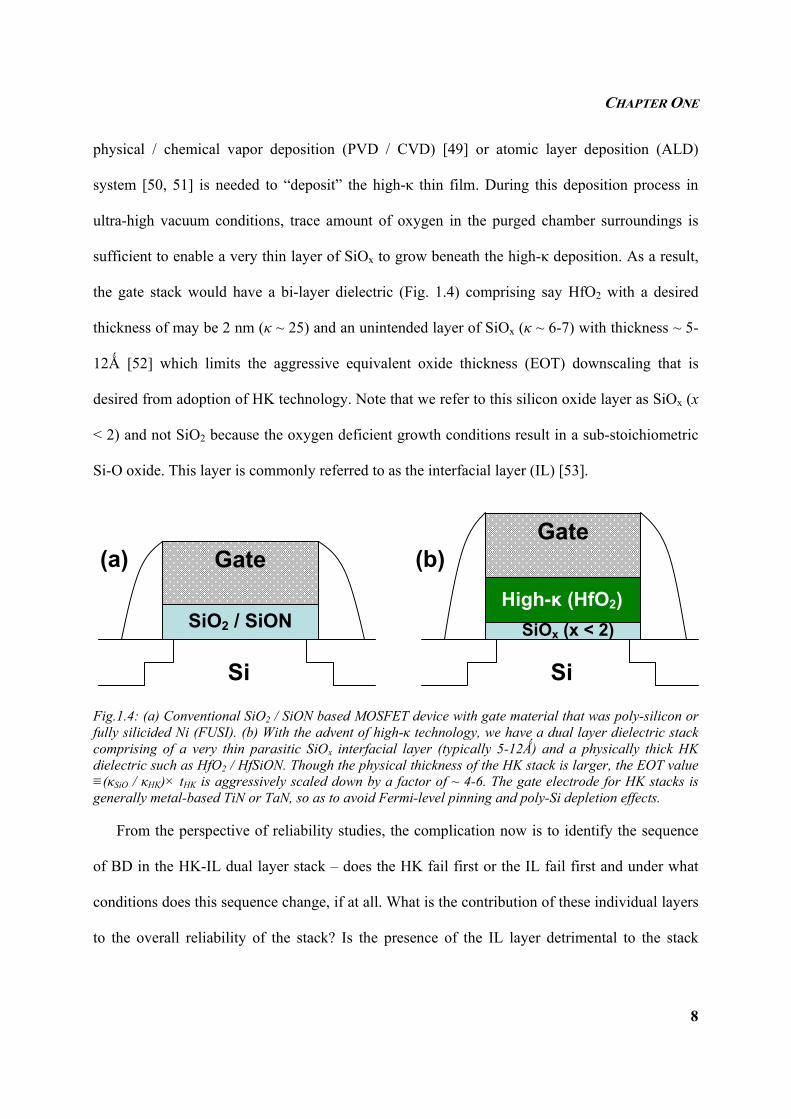
CHAPTER ONE
8
physical / chemical vapor deposition (PVD / CVD) [49] or atomic layer deposition (ALD)
system [50, 51] is needed to “deposit” the high-κ thin film. During this deposition process in
ultra-high vacuum conditions, trace amount of oxygen in the purged chamber surroundings is
sufficient to enable a very thin layer of SiOx to grow beneath the high-κ deposition. As a result,
the gate stack would have a bi-layer dielectric (Fig. 1.4) comprising say HfO2 with a desired
thickness of may be 2 nm (κ ~ 25) and an unintended layer of SiOx (κ ~ 6-7) with thickness ~ 5-
12Ǻ [52] which limits the aggressive equivalent oxide thickness (EOT) downscaling that is
desired from adoption of HK technology. Note that we refer to this silicon oxide layer as SiOx (x
< 2) and not SiO2 because the oxygen deficient growth conditions result in a sub-stoichiometric
Si-O oxide. This layer is commonly referred to as the interfacial layer (IL) [53].
Fig.1.4: (a) Conventional SiO2 / SiON based MOSFET device with gate material that was poly-silicon or fully silicided Ni (FUSI). (b) With the advent of high-κ technology, we have a dual layer dielectric stack comprising of a very thin parasitic SiOx interfacial layer (typically 5-12Ǻ) and a physically thick HK dielectric such as HfO2 / HfSiON. Though the physical thickness of the HK stack is larger, the EOT value ≡(κSiO / κHK)× tHK is aggressively scaled down by a factor of ~ 4-6. The gate electrode for HK stacks is generally metal-based TiN or TaN, so as to avoid Fermi-level pinning and poly-Si depletion effects.
From the perspective of reliability studies, the complication now is to identify the sequence
of BD in the HK-IL dual layer stack – does the HK fail first or the IL fail first and under what
conditions does this sequence change, if at all. What is the contribution of these individual layers
to the overall reliability of the stack? Is the presence of the IL layer detrimental to the stack
SiO2 / SiON
Gate
Si
Gate
Si
SiOx (x < 2) High-κ (HfO2)
(a) (b)
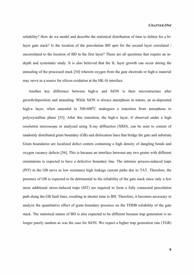
CHAPTER ONE
9
reliability? How do we model and describe the statistical distribution of time to failure for a bi-
layer gate stack? Is the location of the percolation BD spot for the second layer correlated /
uncorrelated to the location of BD in the first layer? These are all questions that require an in-
depth and systematic study. It is also believed that the IL layer growth can occur during the
annealing of the processed stack [54] wherein oxygen from the gate electrode or high-κ material
may serve as a source for silicon oxidation at the HK-Si interface.
Another key difference between high-κ and SiON is their microstructure after
growth/deposition and annealing. While SiON is always amorphous in nature, an as-deposited
high-κ layer, when annealed to 500-6000C undergoes a transition from amorphous to
polycrystalline phase [55]. After this transition, the high-κ layer, if observed under a high
resolution microscope or analyzed using X-ray diffraction (XRD), can be seen to consist of
randomly distributed grain boundary (GB) and dislocation lines that bridge the gate and substrate.
Grain boundaries are localized defect centers containing a high density of dangling bonds and
oxygen vacancy defects [56]. This is because an interface between any two grains with different
orientations is expected to have a defective boundary line. The intrinsic process-induced traps
(PIT) in the GB serve as low resistance high leakage current paths due to TAT. Therefore, the
presence of GB is expected to be detrimental to the reliability of the gate stack since only a few
more additional stress-induced traps (SIT) are required to form a fully connected percolation
path along the GB fault lines, resulting in shorter time to BD. Therefore, it becomes necessary to
analyze the quantitative effect of grain boundary presence on the TDDB reliability of the gate
stack. The statistical nature of BD is also expected to be different because trap generation is no
longer purely random as was the case for SiON. We expect a higher trap generation rate (TGR)
CHAPTER ONE
10
along or adjacent to the GB fault lines. This further motivates us to probe the statistical nature of
BD in high-κ based thin films.
Fig.1.5: (a) Schematic showing the amorphous microstructure with very few process induced traps during HK deposition followed by the standard annealing process which causes the HK to evolve into a (b) polycrystalline columnar microstructure with grain boundary lines. Even the defects existing in the bulk tend to migrate (as indicated by the arrows) and segregate towards the GB [57] (which acts as a sink for vacancies) as governed by the thermodynamics of lowering the system free energy. These GB lines therefore function as “weakest link” and given their low activation energy for vacancy diffusion, it is also possible for the vacancies to preferentially accumulate at the HK-IL interface. Also, notice the increase in the IL layer thickness due to the annealing process.
The interface between the dielectric layers and their adjacent gate / substrate material also
has a significant effect on the reliability of the gate stack [58]. While poly-Si gate – SiO2 and
SiO2-Si interfaces had an intrinsically low defect density, the HK-IL interface generally tends to
be very defective [59, 60] owing to the different material properties. As a result, the negative
contribution of the defective interface to the overall TDDB reliability also needs to be analyzed.
The gate electrode material is also suggested to play an important role in the breakdown and
subsequent recovery (trap passivation) process. While poly-Si gate material based stacks tend to
show superior reliability, the imperative shift from poly-Si to metal gates (MG) such as NiSi
(FUSI), TiN and TaN has a detrimental effect on the oxide BD process owing to the tendency of
the metal atoms to migrate (punch through) into the oxide at sufficiently high electric fields
and/or temperature conditions [61, 62]. Since SiON technology was predominantly based on the
Amorphous HfO2
Annealing
SiOx (IL) SiOx (IL)
Polycrystalline HfO2 Columnar Microstructure
CHAPTER ONE
11
conventional poly-Si gate, while high-κ technology involves the integration of MG to avoid
poly-depletion and Fermi-level pinning effects [63], the impact of the metal electrode on HK
reliability also needs to be investigated. It is still largely unclear whether the role of the MG is
still detrimental to TDDB at very low operating voltage conditions of Vop = 1V.
The metal gate electrodes tend to show a unique “oxygen-gettering” property characteristic
of their high intrinsic oxygen solubility [64]. Making use of this property may help in
“recovering” the BD of the oxide by initiating reverse migration of oxygen ions (O2-) stored in
the MG by application of an opposite polarity bias which can “passivate” the oxygen vacancy
(V02+) traps in the dielectric thereby “repairing” the device, “shutting-off” the percolation path
and “rejuvenating” device performance. This interesting oxygen solubility property of the metal
gate inspired us to investigate into the novel possibility of breakdown recovery and “self-repair”
of an integrated circuit, which could be very impactful to the industry in boosting reliability
margins. The oxygen gettering property of MG could also help us to understand the fundamental
mechanism of RESET (LRS → HRS transition) in the RRAM [48], which may be similar to the
recovery mentioned above.
Lastly, there is a driving force in the industry to try and eliminate the presence of the IL layer
as it limits the ability to aggressively scale down the EOT of sub-16 nm technology node devices
[65, 66]. One of the techniques proposed to achieve a zero IL layer (ZIL) solution is to use the
oxygen gettering MG to induce the reduction of SiOx → Si [67]. Though initial efforts from a
process technology perspective have shown positive results, the reliability of a ZIL gate stack is
still questionable considering that the grain boundary lines in the HK would directly short the
gate to the substrate in the absence of the IL layer. This motivates us to try and investigate the
impact of a ZIL solution on the TDDB reliability of advanced future logic device technology
CHAPTER ONE
12
nodes. It is worth noting that direct contact of high-κ on silicon is known to suffer from thermal
instability issues as well [68, 69].
1.3 OBJECTIVES OF STUDY
Based on the motivations highlighted in the previous section, the specific objectives of the
study are listed below, each of which shall be addressed in detail in the subsequent chapters.
To determine the sequence of BD in a dual layer HK-IL stack and identify whether the IL
or HK is the first layer to breakdown. The dependence of the BD sequence on the ratio of
HK to IL layer thickness (tHK : tIL) and applied gate voltage (Vg), if any, will also be probed.
To carry out a quantitative reliability study of HK-IL dual layer stacks using accelerated
life test (ALT) approach and failure time extrapolation. This involves decoding the role of
the individual HK and IL layers and identifying their individual contributions to the gate
stack reliability. The statistical failure distribution of HK-IL failures will be studied to find
out whether application of Weibull distribution is still valid. In the case of a non-Weibull
stochastic trend, the reasons for deviation from Weibull distribution will be investigated.
To modify the existing percolation model which is only valid for uniform trap generation
and incorporate the role of grain boundaries in polycrystalline high-κ films which serve as
localized defect centers with enhanced trap generation rate. This model will help to explain
the various statistical trends unique to high-κ gate stacks.
To carry out a feasibility study from a materials perspective on the metal migration from
the gate electrode into the dielectric resulting in metal filamentation failure. The purpose of
this analysis is to find out whether HBD induced by metal migration would ever occur in
the MG-HK stacks.
CHAPTER ONE
13
To identify the pitfalls, if any, in the current approach of reliability assessment and
extrapolation for HK gate stacks. The purpose here is to find out whether the empirical
extrapolation of percentile time to failure that we carry out by default from high to low
voltage stress conditions is valid from a physics point of view [70]. In other words, is the
assumption of the same failure mechanism at low (Vop = 1V) and high (Vstress = 3-4V)
voltage stress conditions valid?
To assess the feasibility of implementing a zero IL (ZIL) layer gate stack for sub-16 nm
technology nodes from a reliability point of view.
To investigate the novel possibility of using “oxygen gettering” metal gate electrodes as a
design for reliability (DFR) tool to passivate the oxygen vacancy traps (V02+) so as to
recover the BD event and “shut-off” the percolation path thereby improving the device
performance and prolonging the TDDB lifetime in the operational stage.
To correlate the breakdown and recovery phenomena in M-I-S logic stacks to the SET and
RESET switching process in M-I-M stacks for resistive switching memory (RRAM)
considering the similar materials used in the two different device technologies. The aim is
to take advantage of our in-depth understanding of the physics of failure in MG-HK logic
devices and apply it to explain the fundamentals governing resistive switching. As it stands,
most reports on RRAM mechanisms tend to be speculative without physical analysis
justification [71].
To quantify the retention reliability and read disturb immunity of RRAM based on our
understanding of the noise phenomena in logic devices and the TDDB failures which we
study extensively. The retention lifetime in the HRS state is analogous to the TDDB
CHAPTER ONE
14
process and the retention lifetime in the LRS state may be related to the thermodynamics
and kinetics of trap passivation using oxygen ions from the metal gate.
It is worth noting that for all the RRAM related studies here, we make use of the
conventional logic MOS transistor as the test structure. All devices (both SiON and high-κ based
stacks) tested in this study are of industrial quality and were provided by our research
collaborators at the Interuniversity Microelectronics Center (IMEC), Leuven, Belgium and
Global Foundries®, Singapore.
1.4 ORGANIZATION OF THESIS
This thesis is divided into seven major chapters. The organization of this thesis is presented as
follows:
• Chapter Two is a literature review of the relevant research work carried out on the various
topics we intend to address relating to high-κ breakdown and resistive switching.
• Chapter Three focuses on the new test methodology proposed to initiate a two-stage
sequential BD of the HK-IL stack and presents various electrical characterization techniques
used to identify the sequence of BD.
• Chapter Four is a comprehensive study on the reliability modeling and statistical nature of
HK-IL breakdown considering the effects of microstructural variations in polycrystalline HK
gate stacks.
• Chapter Five investigates into the possibility of reversible breakdown in logic stacks with
oxygen gettering metal electrodes and transfers this understanding to the mechanism
governing the resistive switching phenomenon.
CHAPTER ONE
15
• Chapter Six presents the electrical test results of switching trends in the logic gate stack and
discusses the possibility of realizing a dual mode switching RRAM device depending on the
compliance capping for forming / SET transitions.
• Chapter Seven is a brief study of the retention reliability and read disturb immunity in
RRAM based on its analogy with the TDDB phenomenon and the thermodynamics of trap
passivation / metal filament rupture.
• Chapter Eight presents the conclusions of this project and highlights the need and direction
for future research work in this area.
1.5 SPECIFIC CONTRIBUTIONS
The specific contributions of this study include - (1) a new electrical test algorithm that
enables separate sequential BD of the HK and IL layers, (2) identifying IL to be the first layer to
BD in the dual layer gate stack, (3) relating the convex non-Weibull failure distributions for
TDDB to the two-layer oxide stack and the grain boundary defects in the HK film, (4) use of
oxygen gettering metal electrodes to achieve SBD reversibility thereby prolonging the TDDB
lifetime, (5) proposal of a dual mode switching RRAM with two different compliance controlled
switching mechanisms governed by oxygen vacancies and metallic nanofilaments, (6)
understanding the pseudo-random / random nature of filament nucleation and rupture in RRAM
for multiple switching cycles using electrical characterization techniques to detect the location of
BD given a transistor test structure, (7) extending the device level reliability results to the circuit
level to conclude that failure at circuit level operating conditions can only occur by multiple IL
BD events, as opposed to a sequential HK-IL BD event and (8) documenting the need for higher
read voltages for RRAM to ensure prolonged retention and improved noise immunity.
CHAPTER ONE
16
The results from the accomplished work have been published in premier international
conferences such as the IEEE International Reliability Physics Symposium (IRPS), USA and
Insulating Films on Semiconductors (INFOS), France symposium, as well as prestigious peer-
reviewed journals, such as the IEEE Electron Device Letters (EDL), Applied Physics Letters
(APL) and Microelectronic Engineering.
CHAPTER TWO
17
CHAPTER TWO
LLLIIITTTEEERRRAAATTTUUURRREEE RRREEEVVVIIIEEEWWW
2.1 INTRODUCTION
In the first chapter, we discussed the motivation and objectives of this project in sufficient
detail and highlighted the specific contributions achieved in the study. This chapter is a follow-
up of the background section presented earlier in Section 1.1 to give a more holistic view of the
results that have been achieved in the recent past by various academic and industrial research
groups working on high-κ logic reliability characterization and resistive switching memory
technology.
We take an investigative approach into the past results published by various research groups
in order to identify their shortcomings, assumptions, limitations and drawbacks. This paves way
for us to identify the critical issues and problems to be solved, which will then be addressed in
the results sections from Chapters 3-7.
The literature review is divided into two main parts – Section 2.2 reviews the work on high-κ
logic gate stack reliability and Section 2.3 reviews the current understanding of the resistive
switching mechanism. Each of these sections will have a flow of content as shown in Fig. 2.1.
We start with the (a) fabrication and process characterization stage followed by (b) electrical
characterization, (c) reliability testing and statistical analysis and lastly (d) physical / chemical
analysis of the failed-logic / operated-memory device using high resolution microscopic tools
such as transmission electron microscopy (TEM) and scanning tunneling microscopy (STM).
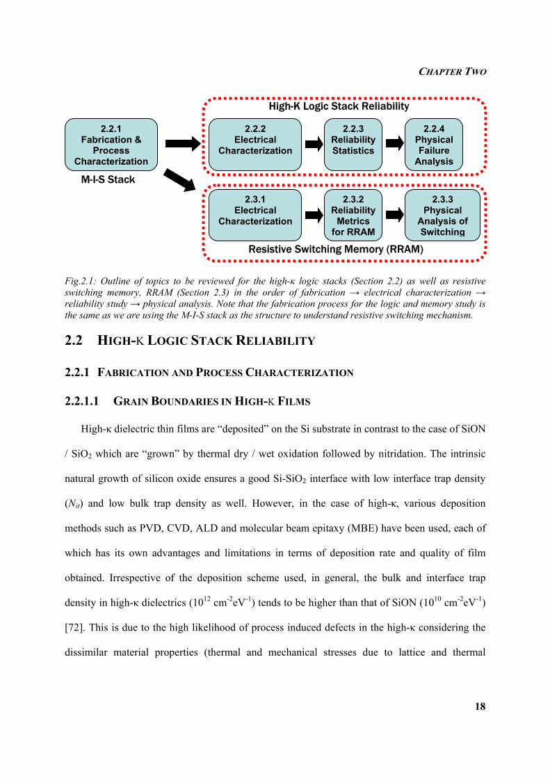
CHAPTER TWO
18
Fig.2.1: Outline of topics to be reviewed for the high-κ logic stacks (Section 2.2) as well as resistive switching memory, RRAM (Section 2.3) in the order of fabrication → electrical characterization → reliability study → physical analysis. Note that the fabrication process for the logic and memory study is the same as we are using the M-I-S stack as the structure to understand resistive switching mechanism.
2.2 HIGH-Κ LOGIC STACK RELIABILITY
2.2.1 FABRICATION AND PROCESS CHARACTERIZATION
2.2.1.1 GRAIN BOUNDARIES IN HIGH-Κ FILMS
High-κ dielectric thin films are “deposited” on the Si substrate in contrast to the case of SiON
/ SiO2 which are “grown” by thermal dry / wet oxidation followed by nitridation. The intrinsic
natural growth of silicon oxide ensures a good Si-SiO2 interface with low interface trap density
(Nit) and low bulk trap density as well. However, in the case of high-κ, various deposition
methods such as PVD, CVD, ALD and molecular beam epitaxy (MBE) have been used, each of
which has its own advantages and limitations in terms of deposition rate and quality of film
obtained. Irrespective of the deposition scheme used, in general, the bulk and interface trap
density in high-κ dielectrics (1012 cm-2eV-1) tends to be higher than that of SiON (1010 cm-2eV-1)
[72]. This is due to the high likelihood of process induced defects in the high-κ considering the
dissimilar material properties (thermal and mechanical stresses due to lattice and thermal
2.2.1 Fabrication &
Process Characterization
2.2.2 Electrical
Characterization
2.2.3 ReliabilityStatistics
2.2.4 Physical Failure
Analysis
2.3.1 Electrical
Characterization
2.3.2 Reliability
Metrics for RRAM
2.3.3 Physical
Analysis of Switching
High-K Logic Stack Reliability
Resistive Switching Memory (RRAM)
M-I-S Stack
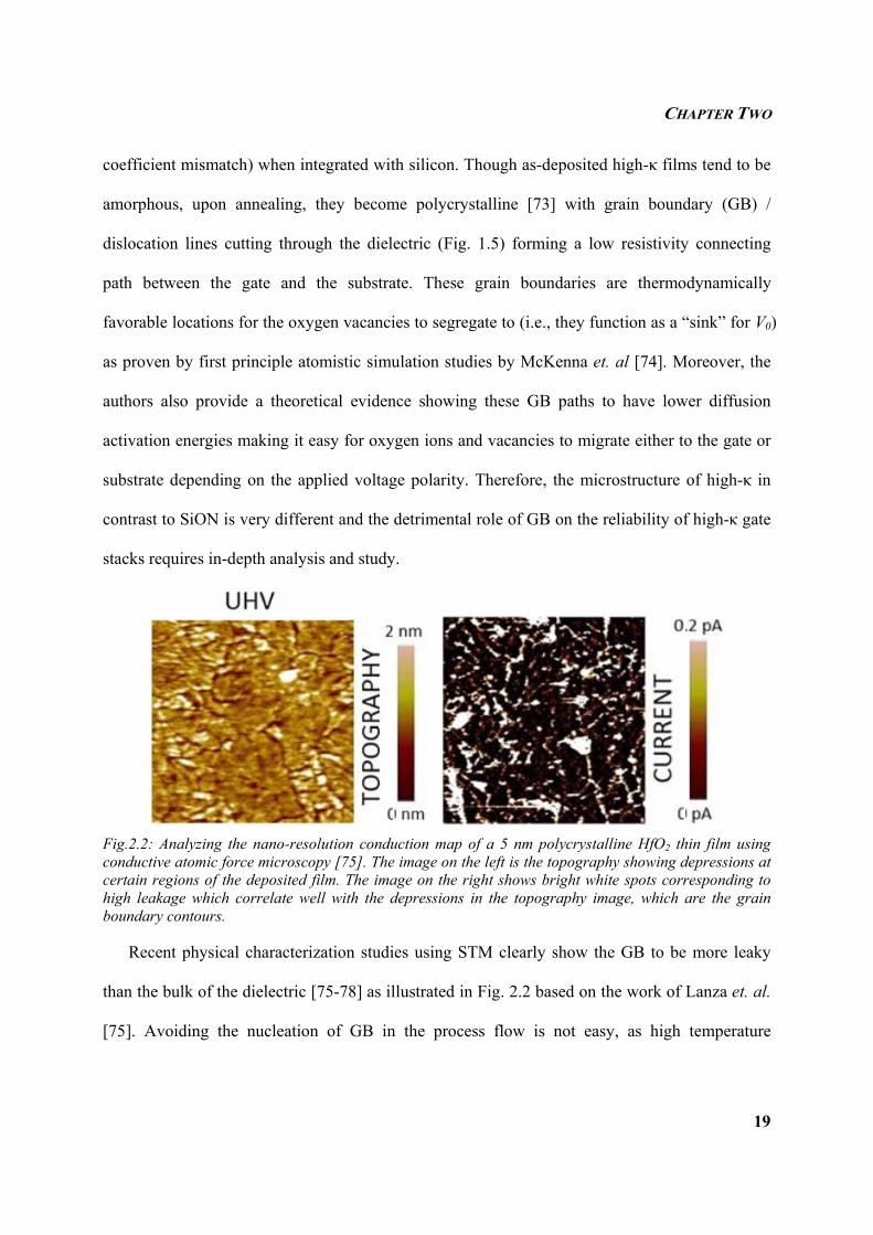
CHAPTER TWO
19
coefficient mismatch) when integrated with silicon. Though as-deposited high-κ films tend to be
amorphous, upon annealing, they become polycrystalline [73] with grain boundary (GB) /
dislocation lines cutting through the dielectric (Fig. 1.5) forming a low resistivity connecting
path between the gate and the substrate. These grain boundaries are thermodynamically
favorable locations for the oxygen vacancies to segregate to (i.e., they function as a “sink” for V0)
as proven by first principle atomistic simulation studies by McKenna et. al [74]. Moreover, the
authors also provide a theoretical evidence showing these GB paths to have lower diffusion
activation energies making it easy for oxygen ions and vacancies to migrate either to the gate or
substrate depending on the applied voltage polarity. Therefore, the microstructure of high-κ in
contrast to SiON is very different and the detrimental role of GB on the reliability of high-κ gate
stacks requires in-depth analysis and study.
Fig.2.2: Analyzing the nano-resolution conduction map of a 5 nm polycrystalline HfO2 thin film using conductive atomic force microscopy [75]. The image on the left is the topography showing depressions at certain regions of the deposited film. The image on the right shows bright white spots corresponding to high leakage which correlate well with the depressions in the topography image, which are the grain boundary contours.
Recent physical characterization studies using STM clearly show the GB to be more leaky
than the bulk of the dielectric [75-78] as illustrated in Fig. 2.2 based on the work of Lanza et. al.
[75]. Avoiding the nucleation of GB in the process flow is not easy, as high temperature
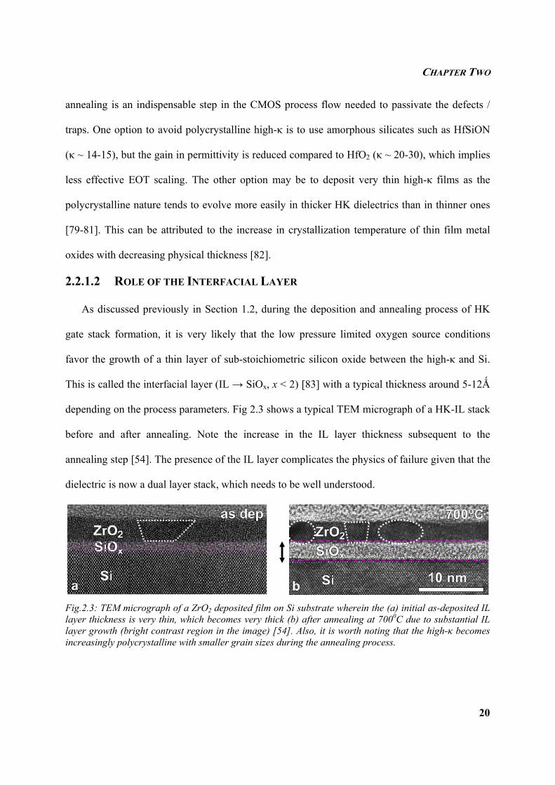
CHAPTER TWO
20
annealing is an indispensable step in the CMOS process flow needed to passivate the defects /
traps. One option to avoid polycrystalline high-κ is to use amorphous silicates such as HfSiON
(κ ~ 14-15), but the gain in permittivity is reduced compared to HfO2 (κ ~ 20-30), which implies
less effective EOT scaling. The other option may be to deposit very thin high-κ films as the
polycrystalline nature tends to evolve more easily in thicker HK dielectrics than in thinner ones
[79-81]. This can be attributed to the increase in crystallization temperature of thin film metal
oxides with decreasing physical thickness [82].
2.2.1.2 ROLE OF THE INTERFACIAL LAYER
As discussed previously in Section 1.2, during the deposition and annealing process of HK
gate stack formation, it is very likely that the low pressure limited oxygen source conditions
favor the growth of a thin layer of sub-stoichiometric silicon oxide between the high-κ and Si.
This is called the interfacial layer (IL → SiOx, x < 2) [83] with a typical thickness around 5-12Ǻ
depending on the process parameters. Fig 2.3 shows a typical TEM micrograph of a HK-IL stack
before and after annealing. Note the increase in the IL layer thickness subsequent to the
annealing step [54]. The presence of the IL layer complicates the physics of failure given that the
dielectric is now a dual layer stack, which needs to be well understood.
Fig.2.3: TEM micrograph of a ZrO2 deposited film on Si substrate wherein the (a) initial as-deposited IL layer thickness is very thin, which becomes very thick (b) after annealing at 7000C due to substantial IL layer growth (bright contrast region in the image) [54]. Also, it is worth noting that the high-κ becomes increasingly polycrystalline with smaller grain sizes during the annealing process.
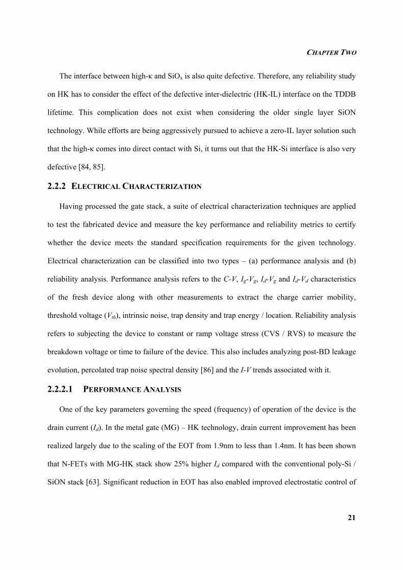
CHAPTER TWO
21
The interface between high-κ and SiOx is also quite defective. Therefore, any reliability study
on HK has to consider the effect of the defective inter-dielectric (HK-IL) interface on the TDDB
lifetime. This complication does not exist when considering the older single layer SiON
technology. While efforts are being aggressively pursued to achieve a zero-IL layer solution such
that the high-κ comes into direct contact with Si, it turns out that the HK-Si interface is also very
defective [84, 85].
2.2.2 ELECTRICAL CHARACTERIZATION
Having processed the gate stack, a suite of electrical characterization techniques are applied
to test the fabricated device and measure the key performance and reliability metrics to certify
whether the device meets the standard specification requirements for the given technology.
Electrical characterization can be classified into two types – (a) performance analysis and (b)
reliability analysis. Performance analysis refers to the C-V, Ig-Vg, Id-Vg and Id-Vd characteristics
of the fresh device along with other measurements to extract the charge carrier mobility,
threshold voltage (Vth), intrinsic noise, trap density and trap energy / location. Reliability analysis
refers to subjecting the device to constant or ramp voltage stress (CVS / RVS) to measure the
breakdown voltage or time to failure of the device. This also includes analyzing post-BD leakage
evolution, percolated trap noise spectral density [86] and the I-V trends associated with it.
2.2.2.1 PERFORMANCE ANALYSIS
One of the key parameters governing the speed (frequency) of operation of the device is the
drain current (Id). In the metal gate (MG) – HK technology, drain current improvement has been
realized largely due to the scaling of the EOT from 1.9nm to less than 1.4nm. It has been shown
that N-FETs with MG-HK stack show 25% higher Id compared with the conventional poly-Si /
SiON stack [63]. Significant reduction in EOT has also enabled improved electrostatic control of
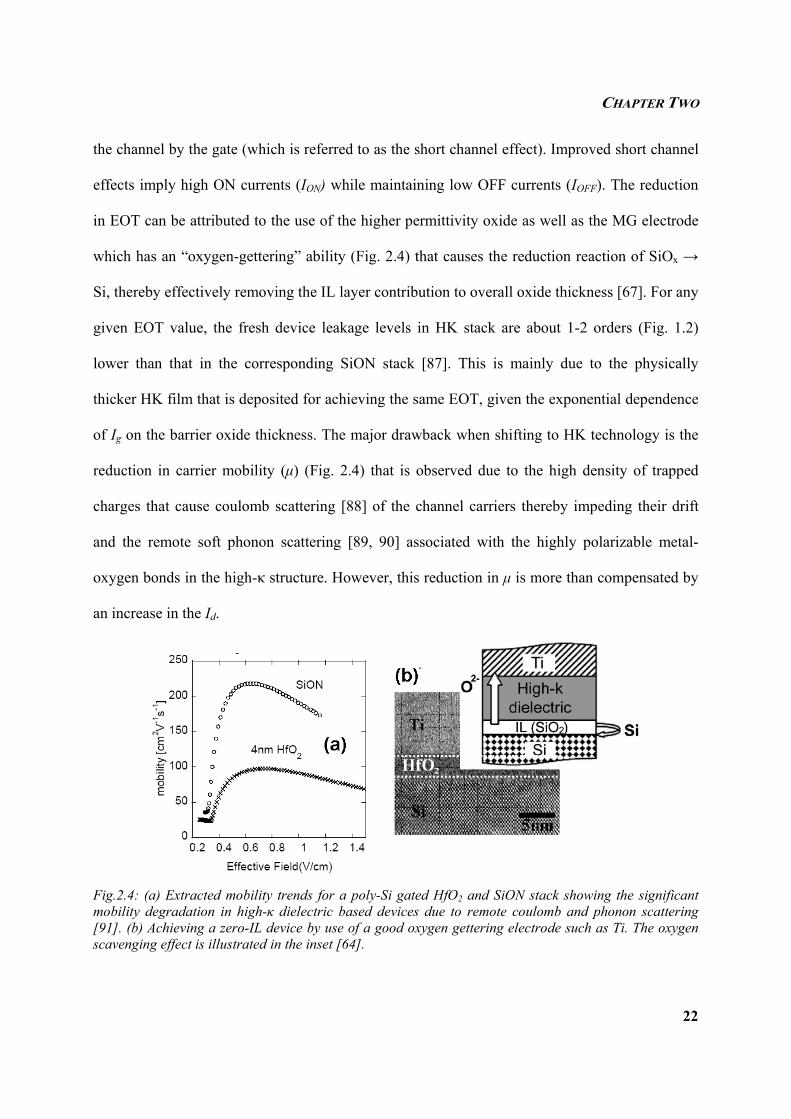
CHAPTER TWO
22
the channel by the gate (which is referred to as the short channel effect). Improved short channel
effects imply high ON currents (ION) while maintaining low OFF currents (IOFF). The reduction
in EOT can be attributed to the use of the higher permittivity oxide as well as the MG electrode
which has an “oxygen-gettering” ability (Fig. 2.4) that causes the reduction reaction of SiOx →
Si, thereby effectively removing the IL layer contribution to overall oxide thickness [67]. For any
given EOT value, the fresh device leakage levels in HK stack are about 1-2 orders (Fig. 1.2)
lower than that in the corresponding SiON stack [87]. This is mainly due to the physically
thicker HK film that is deposited for achieving the same EOT, given the exponential dependence
of Ig on the barrier oxide thickness. The major drawback when shifting to HK technology is the
reduction in carrier mobility (µ) (Fig. 2.4) that is observed due to the high density of trapped
charges that cause coulomb scattering [88] of the channel carriers thereby impeding their drift
and the remote soft phonon scattering [89, 90] associated with the highly polarizable metal-
oxygen bonds in the high-κ structure. However, this reduction in µ is more than compensated by
an increase in the Id.
Fig.2.4: (a) Extracted mobility trends for a poly-Si gated HfO2 and SiON stack showing the significant mobility degradation in high-κ dielectric based devices due to remote coulomb and phonon scattering [91]. (b) Achieving a zero-IL device by use of a good oxygen gettering electrode such as Ti. The oxygen scavenging effect is illustrated in the inset [64].
CHAPTER TWO
23
2.2.2.2 RELIABILITY ANALYSIS
A. DIELECTRIC BREAKDOWN FIELD STRENGTH
From a reliability perspective, one of the key factors to consider is the critical breakdown
field (ξBD) of the oxide material which is an intrinsic material property depending on the
activation energy for bond breakage and the bond polarization factor. It turns out that high-κ
dielectrics tend to have a much lower ξBD ~ 4-7 MV/cm as compared to SiO2 which shows ξBD ~
15 MV/cm (Fig. 2.5(a)). It can be shown using thermodynamics that the BD field has an
approximately inverse square root relationship to the permittivity of the oxide [92]. Although HK
has a lower ξBD, the physically thicker film for the same EOT value ensures that the voltage to
BD (VBD) is relatively high. For aggressively scaled EOT devices with zero-IL layer stack, the
low ξBD of high-κ materials could play a detrimental role in severely limiting operational lifetime.
Fig.2.5: (a) Trend of variation in the dielectric breakdown strength with the permittivity of the material [93]. The solid line is the trend of variation which closely matches with theoretical predictions of an inverse square root law. (b) Typical trends of TDDB in a dual layer HfO2-SiOx gate stack at various stress conditions [94].
B. TIME DEPENDENT DIELECTRIC BREAKDOWN
Time dependent dielectric breakdown (TDDB) is the most important and standard industrial
reliability metric which is tested and measured using accelerated life stress tests (ALT). A
conventional TDDB study includes subjecting at least 10-20 devices for every combination of
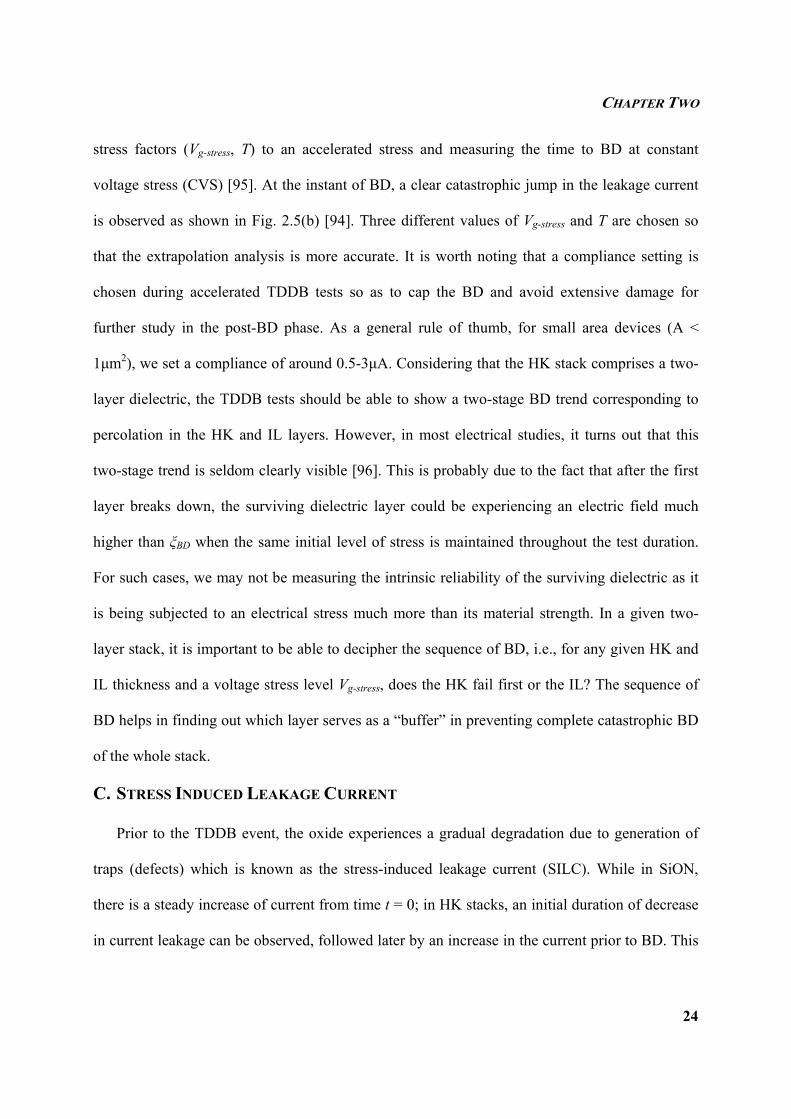
CHAPTER TWO
24
stress factors (Vg-stress, T) to an accelerated stress and measuring the time to BD at constant
voltage stress (CVS) [95]. At the instant of BD, a clear catastrophic jump in the leakage current
is observed as shown in Fig. 2.5(b) [94]. Three different values of Vg-stress and T are chosen so
that the extrapolation analysis is more accurate. It is worth noting that a compliance setting is
chosen during accelerated TDDB tests so as to cap the BD and avoid extensive damage for
further study in the post-BD phase. As a general rule of thumb, for small area devices (A <
1µm2), we set a compliance of around 0.5-3µA. Considering that the HK stack comprises a two-
layer dielectric, the TDDB tests should be able to show a two-stage BD trend corresponding to
percolation in the HK and IL layers. However, in most electrical studies, it turns out that this
two-stage trend is seldom clearly visible [96]. This is probably due to the fact that after the first
layer breaks down, the surviving dielectric layer could be experiencing an electric field much
higher than ξBD when the same initial level of stress is maintained throughout the test duration.
For such cases, we may not be measuring the intrinsic reliability of the surviving dielectric as it
is being subjected to an electrical stress much more than its material strength. In a given two-
layer stack, it is important to be able to decipher the sequence of BD, i.e., for any given HK and
IL thickness and a voltage stress level Vg-stress, does the HK fail first or the IL? The sequence of
BD helps in finding out which layer serves as a “buffer” in preventing complete catastrophic BD
of the whole stack.
C. STRESS INDUCED LEAKAGE CURRENT
Prior to the TDDB event, the oxide experiences a gradual degradation due to generation of
traps (defects) which is known as the stress-induced leakage current (SILC). While in SiON,
there is a steady increase of current from time t = 0; in HK stacks, an initial duration of decrease
in current leakage can be observed, followed later by an increase in the current prior to BD. This
CHAPTER TWO
25
initial regime of reduction in leakage current has been ascribed to the charge trapping
phenomenon, specific to HK gate stacks [97]. Some studies reveal that though the initial leakage
current is low in HK stacks due to the physically thicker oxide, the relative rate of increase in
current in the SILC stage (∆Ig/Ig) is about two orders of magnitude higher in the HK as compared
to SiON, which limits the advantage of adopting the HK technology for the future [98]. Within a
short duration, the SILC induced leakage current in HK may exceed that of the SiON (for the
same EOT) due to the high defect generation rate. This enhanced rate of trap generation could be
either due to difficulty in achieving good quality deposited oxides or an intrinsic property of the
HK material itself. Fig. 2.6 is an example showing the SILC trends in a HfO2-based stack with
the initial duration of leakage current reduction due to charge trapping [94].
Fig.2.6: Trend of leakage current evolution with time in a HfO2-based stack with an initial duration of charge trapping in the process induced traps that causes current to decrease and reach a minimum. When charge trapping saturates, the TAT current induced by additional trap generation starts to dominate and the leakage current henceforth increases. The figure on the right is the obtained by extracting the charge trapping component out of the test data in the left figure [94].
D. POST BREAKDOWN PHASE – DIGITAL FLUCTUATIONS
Immediately after the TDDB stage, clear discrete digital step-like fluctuations have been
observed in Ig and Id at low voltages for the SiON. These fluctuations have been studied for
SiON in sufficient detail and are attributed to the trapping (capture) and detrapping (emission)
[99] of electron charge carriers in the oxygen vacancy defects (traps) that constitute the
CHAPTER TWO
26
percolation path. This capture-emission process is Markovian stochastic (random) [100] and
therefore these fluctuations are referred to as random telegraph noise (RTN) [99]. The effect of
RTN is that the post-BD leakage current trends can fluctuate quite a bit by about an order of
magnitude depending on the instantaneous configuration of the traps → traps with electrons
captured cannot assist in the TAT conduction process and are termed as “off” / “inactive”, while
traps which are empty due to emitted carriers can assist in the carrier transport and are termed as
“on” / “active”. Assuming there are say 3 traps in the percolation path, we would have 23 = 8
different states / levels of Ig fluctuation. On a positive note, the presence of RTN implies that
post-BD Ig-Vg trends can at times be very close to the fresh device leakage depending on the on-
off configuration of the traps [101]. This implies that the even after BD, the device performance
is only marginally affected and therefore, there is an initial duration in the post-BD regime when
the device (circuit) can still function effectively. The RTN regime is hence a “boost” to the
device reliability and provides for an enhanced reliability margin in SiON. However, on the
negative side, the stochastic nature of RTN (especially in the post-BD stage) induces significant
variability in the performance of the device (drain current, Id and threshold voltage, Vth) and the
circuit.
While most studies in the past analyzed the digital fluctuations in the drain current (Id) [102],
there are more recent investigations that probe similar fluctuations in Ig and correlate them with
the Id [103]. In other words, the fluctuations originate from the traps in the oxide, but their
response can be measured by either Ig or Id. Note that RTN studies can be carried out both at the
pre-BD SILC stage as well as the SBD stage. Since our focus is more from a reliability point of
view, we analyze the noise effects in the SBD stage. For studies relating to the process induced
traps [104], noise is measured on fresh devices and for studies that probe into the kinetics of trap
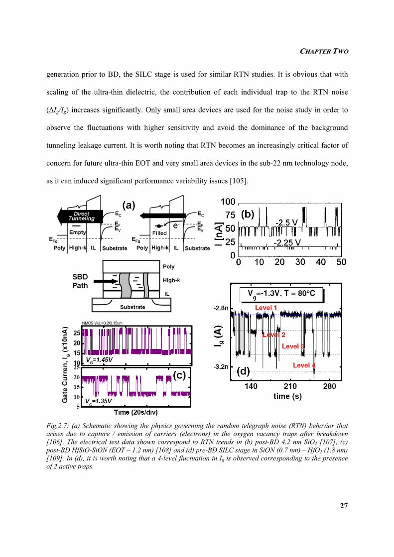
CHAPTER TWO
27
generation prior to BD, the SILC stage is used for similar RTN studies. It is obvious that with
scaling of the ultra-thin dielectric, the contribution of each individual trap to the RTN noise
(∆Ig/Ig) increases significantly. Only small area devices are used for the noise study in order to
observe the fluctuations with higher sensitivity and avoid the dominance of the background
tunneling leakage current. It is worth noting that RTN becomes an increasingly critical factor of
concern for future ultra-thin EOT and very small area devices in the sub-22 nm technology node,
as it can induced significant performance variability issues [105].
Fig.2.7: (a) Schematic showing the physics governing the random telegraph noise (RTN) behavior that arises due to capture / emission of carriers (electrons) in the oxygen vacancy traps after breakdown [106]. The electrical test data shown correspond to RTN trends in (b) post-BD 4.2 nm SiO2 [107], (c) post-BD HfSiO-SiON (EOT ~ 1.2 nm) [108] and (d) pre-BD SILC stage in SiON (0.7 nm) – HfO2 (1.8 nm) [109]. In (d), it is worth noting that a 4-level fluctuation in Ig is observed corresponding to the presence of 2 active traps.
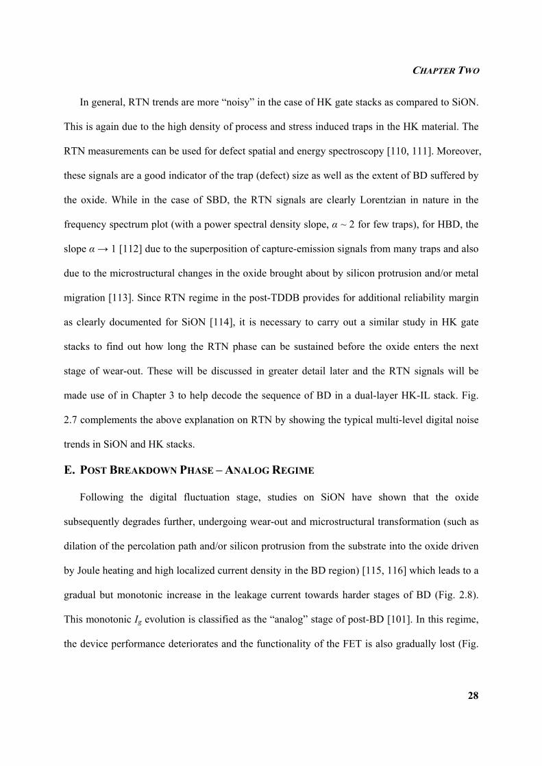
CHAPTER TWO
28
In general, RTN trends are more “noisy” in the case of HK gate stacks as compared to SiON.
This is again due to the high density of process and stress induced traps in the HK material. The
RTN measurements can be used for defect spatial and energy spectroscopy [110, 111]. Moreover,
these signals are a good indicator of the trap (defect) size as well as the extent of BD suffered by
the oxide. While in the case of SBD, the RTN signals are clearly Lorentzian in nature in the
frequency spectrum plot (with a power spectral density slope, α ~ 2 for few traps), for HBD, the
slope α → 1 [112] due to the superposition of capture-emission signals from many traps and also
due to the microstructural changes in the oxide brought about by silicon protrusion and/or metal
migration [113]. Since RTN regime in the post-TDDB provides for additional reliability margin
as clearly documented for SiON [114], it is necessary to carry out a similar study in HK gate
stacks to find out how long the RTN phase can be sustained before the oxide enters the next
stage of wear-out. These will be discussed in greater detail later and the RTN signals will be
made use of in Chapter 3 to help decode the sequence of BD in a dual-layer HK-IL stack. Fig.
2.7 complements the above explanation on RTN by showing the typical multi-level digital noise
trends in SiON and HK stacks.
E. POST BREAKDOWN PHASE – ANALOG REGIME
Following the digital fluctuation stage, studies on SiON have shown that the oxide
subsequently degrades further, undergoing wear-out and microstructural transformation (such as
dilation of the percolation path and/or silicon protrusion from the substrate into the oxide driven
by Joule heating and high localized current density in the BD region) [115, 116] which leads to a
gradual but monotonic increase in the leakage current towards harder stages of BD (Fig. 2.8).
This monotonic Ig evolution is classified as the “analog” stage of post-BD [101]. In this regime,
the device performance deteriorates and the functionality of the FET is also gradually lost (Fig.
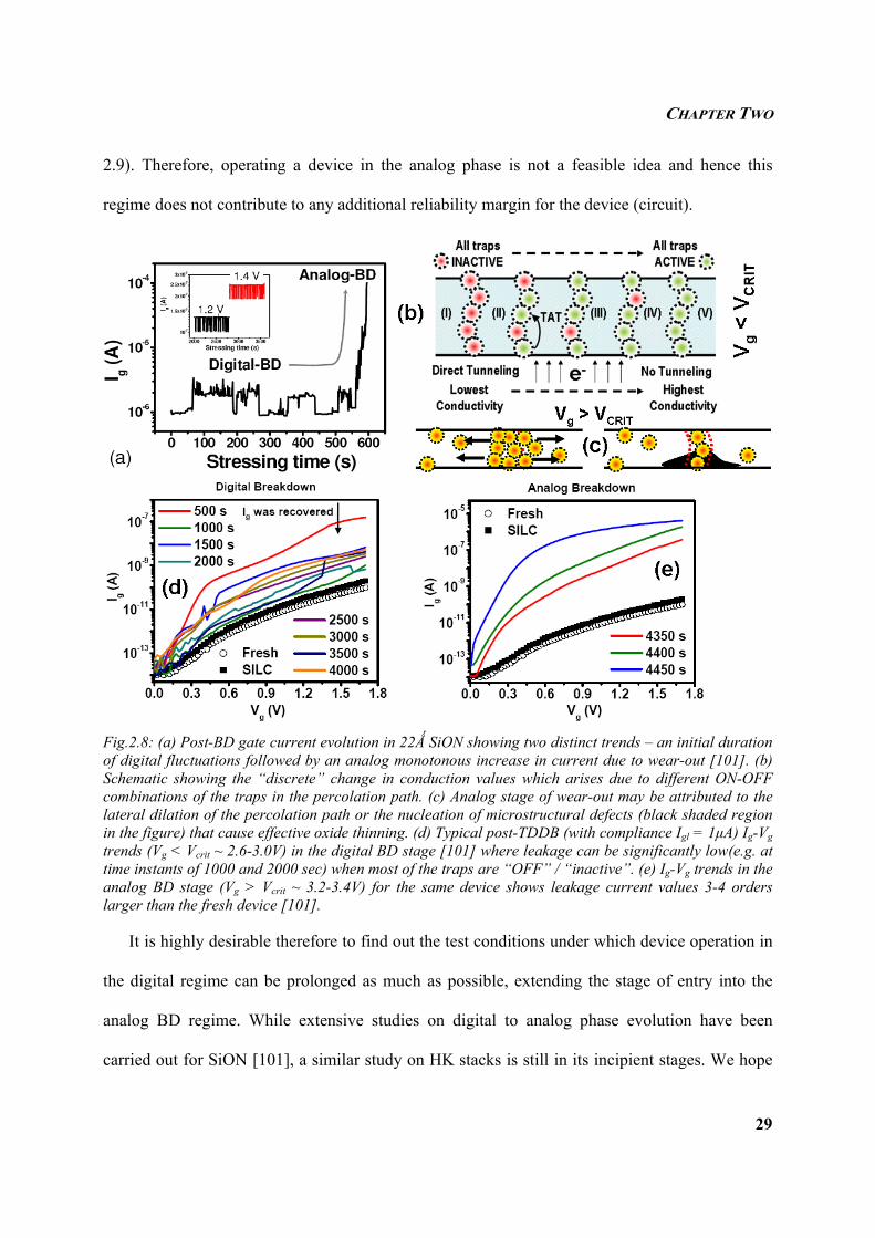
CHAPTER TWO
29
2.9). Therefore, operating a device in the analog phase is not a feasible idea and hence this
regime does not contribute to any additional reliability margin for the device (circuit).
Fig.2.8: (a) Post-BD gate current evolution in 22Ǻ SiON showing two distinct trends – an initial duration of digital fluctuations followed by an analog monotonous increase in current due to wear-out [101]. (b) Schematic showing the “discrete” change in conduction values which arises due to different ON-OFF combinations of the traps in the percolation path. (c) Analog stage of wear-out may be attributed to the lateral dilation of the percolation path or the nucleation of microstructural defects (black shaded region in the figure) that cause effective oxide thinning. (d) Typical post-TDDB (with compliance Igl = 1µA) Ig-Vg trends (Vg < Vcrit ~ 2.6-3.0V) in the digital BD stage [101] where leakage can be significantly low(e.g. at time instants of 1000 and 2000 sec) when most of the traps are “OFF” / “inactive”. (e) Ig-Vg trends in the analog BD stage (Vg > Vcrit ~ 3.2-3.4V) for the same device shows leakage current values 3-4 orders larger than the fresh device [101].
It is highly desirable therefore to find out the test conditions under which device operation in
the digital regime can be prolonged as much as possible, extending the stage of entry into the
analog BD regime. While extensive studies on digital to analog phase evolution have been
carried out for SiON [101], a similar study on HK stacks is still in its incipient stages. We hope
CHAPTER TWO
30
to extend our understanding of SiON post-BD to MG-HK stacks in Chapter 3 to discuss the
additional reliability margins that can be obtained in the digital regime.
Fig.2.9: Typical trends of (a) Id-Vg and (b) Id-Vd degradation ranging from fresh device to post-TDDB digital stage (2µA) and subsequent analog BD stages of 30µA and 60µA in a 16Ǻ poly-Si gated SiON device. While MOS performance trends may be acceptable and functional at SBD digital stage (2µA), it degrades significantly by 30-40% in the analog stage and as shown for the (c) case of HBD [101], functionality is completely lost. The analog stage may not even exist for metal gated devices implying that the digital phase is followed immediately by a catastrophic HBD event.
F. CRITICAL VOLTAGE GOVERNING OXIDE WEAR-OUT
The transition from the digital to analog phase is governed by a critical voltage (Vcrit) [117] in
the SiON dielectric (Fig. 2.8). For Vg < Vcrit, it is reported that the digital phase would be
sufficiently prolonged and in most cases, it may last longer than the standard lifetime target of 10
years for integrated circuits. However for Vg > Vcrit, the digital phase has a very short time span
and there is sufficient driving force for Joule heating, current density and temperature enhanced
trap generation and microstructural change of the oxide causing wear-out and analog BD. In
other words, there is a “positive feedback” [115] of current enhanced temperature temperature
enhanced bond breakage and trap generation trap enhanced post-BD TAT current and
temperature again and so on… This positive feedback is apparently self-sustaining only for Vg >
Vcrit [117]. The concept of Vcrit is interesting and important because if Vop < Vcrit, then we can be
CHAPTER TWO
31
assured that even after SBD, the device can function effectively with minimal performance
deterioration for a prolonged period without undergoing any further wear-out. In general, for
SiON, Vcrit > 2V even for tox ~ 1.2 nm and this parameter shows a linear increase with oxide
thickness for tox > 1.6 nm [117]. The extension of the Vcrit concept and its application to MG-HK-
IL stacks has not been pursued previously and we hope to address this issue in Chapter 3.
G. HARD BREAKDOWN
The ultimate and most critical stage of degradation for a dielectric is the “hard breakdown”
(HBD) stage [118] when the dielectric loses its insulative property completely and becomes very
highly conductive and ohmic in nature. The transistor is regarded as “dead” when it evolves into
the HBD regime (Fig. 2.9). It is therefore necessary to ensure that the occurrence of HBD is
postponed to as long as possible. It is generally reported that a circuit suffers multiple SBD
events before undergoing a HBD [119]. The location of the SBD and HBD may or may not be
correlated to each other [120-122]. The mechanism and physics governing HBD can be more
easily deciphered by performing failure analysis using high resolution transmission electron
microscopy (HRTEM). Some of the possible mechanisms to explain HBD include Si epitaxial
protrusion from the substrate into the oxide (known as dielectric breakdown induced epitaxy
(DBIE)) [115], metal filamentation [62] and punchthrough and formation of a fully oxygen-
depleted Si nano-core in the dielectric [123]. The physical analysis images and driving forces
governing these phenomenon will be dealt with in Section 2.2.4 later.
H. RANDOM TELEGRAPH NOISE EFFECTS
As mentioned previously, RTN, which refers to the fluctuations in the gate (Ig) and drain (Id)
current during device operation due to traps present in the dielectric may also be regarded as a
reliability bottleneck. RTN exists both before (due to process induced traps and traps generated
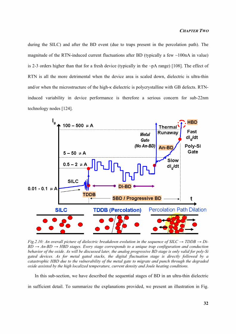
CHAPTER TWO
32
during the SILC) and after the BD event (due to traps present in the percolation path). The
magnitude of the RTN-induced current fluctuations after BD (typically a few ~100nA in value)
is 2-3 orders higher than that for a fresh device (typically in the ~pA range) [108]. The effect of
RTN is all the more detrimental when the device area is scaled down, dielectric is ultra-thin
and/or when the microstructure of the high-κ dielectric is polycrystalline with GB defects. RTN-
induced variability in device performance is therefore a serious concern for sub-22nm
technology nodes [124].
Fig.2.10: An overall picture of dielectric breakdown evolution in the sequence of SILC → TDDB → Di-BD → An-BD → HBD stages. Every stage corresponds to a unique trap configuration and conduction behavior of the oxide. As will be discussed later, the analog progressive BD stage is only valid for poly-Si gated devices. As for metal gated stacks, the digital fluctuation stage is directly followed by a catastrophic HBD due to the vulnerability of the metal gate to migrate and punch through the degraded oxide assisted by the high localized temperature, current density and Joule heating conditions.
In this sub-section, we have described the sequential stages of BD in an ultra-thin dielectric
in sufficient detail. To summarize the explanations provided, we present an illustration in Fig.
CHAPTER TWO
33
2.10 that clearly shows all these stages and the corresponding leakage levels in a small area
device (< 1µm2). It is obvious that post-BD leakage is area-independent (for relatively small area
devices) considering that the localized leakage in the percolated region exceeds the background
area dependent tunneling current.
2.2.3 RELIABILITY STATISTICS
One of the key metrics to assess the feasibility of any new technology node prior to
qualifying it for mass production is its “reliability” which refers to the probability that the device
/ circuit will function at any given time t > 0, when operated under nominal operating conditions
[125]. In the microelectronics arena, the standard reliability criterion is 10 years and for the
oxide, this lifetime target has to be met at the operating voltage, Vop = 1.0-1.1V. Considering the
need for fast time-to-market, it is unrealistic to subject the transistors to a nominal stress level of
Vg = Vop and wait for a prolonged duration of time to observe percolation failures, as this could
take several months or even years [126]. Therefore, we have to resort to accelerated life tests
(ALT) and lifetime extrapolation wherein the devices are subjected to substantially higher
stresses (Vg > Vop) so as to initiate TDDB within a short span of time ~ 10-10000 seconds. There
are a few things to note when using the ALT procedure. The dielectric must not be subjected to
an electric field much more than its critical field strength (ξBD) as this amounts to over-stressing
the insulator beyond its material limits which can cause it to break down instantaneously.
Moreover, we have to make an assumption in the ALT methodology that the failure mechanism
at the use level and accelerated stress conditions is the same [70]. In other words, we are only
accelerating the same FM that we would expect at Vg = Vop. This condition however is not
satisfied in many cases and it turns out that at high ALT stress conditions, the physics of failure
could be very different [70] and new failure mechanisms could be triggered as well. In such
CHAPTER TWO
34
cases, the analysis results from the reliability assessment study become invalid and misleading.
A carefully designed reliability test procedure is therefore needed so as to ensure that we are
testing the right failure mechanism (this is influenced by the leakage conduction / tunneling
transport mechanism), as exemplified by Fig. 2.11(a). Though the reliability assessment
procedure mentioned above is purely statistical, it is critical for the reliability engineer to
understand the physics and internal quantum mechanisms of device operation in order to be able
to apply the right level of ALT stress that accelerates the desired mode / mechanism of failure.
After the dielectric is subjected to ALT stress, the measured time to failure (TTF) data has to be
extrapolated back to Vg = Vop using a life-stress relationship. There are various models used for
extrapolation, which can again be subjective. Some of the popular models used are the inverse
power law (IPL) model [127], field-driven thermochemical ξ-model [128] and anode hole
injection (1/ξ) model [129]. While the ξ and 1/ξ models are based on physical and
phenomenological models respectively, the IPL model is empirical and most commonly used.
The choice of the extrapolation model can alter the field life reliability predictions by many
orders of magnitude, as illustrated in Fig. 2.11(b).
Dielectric breakdown is best described by the Weibull distribution [30], which is the most
relevant one for the case of “weakest link” governed failures. The Weibull distribution is an
extreme-value distribution and it well represents the case when there are many identical and
independent competing processes wherein the first such process that reaches the critical failure
stage (“weakest link”) governs the TTF of the device. This is exactly the case of percolation
breakdown of SiO2 / SiON wherein traps are randomly generated in the amorphous insulator
until they form a connecting chain shorting the gate and substrate at any one location across the
device with area (W × L), where W and L refer to the width and length of the active transistor
CHAPTER TWO
35
channel. The other popular distribution, which is Lognormal, does not describe the dielectric BD
statistics well (Fig. 2.11 (c)) at very low and very high percentile values [130] and this deviation
is expected because the fundamental derivation of the Lognormal is based on the “gradual
multiplicative degradation model” [131], which is very different from the “weakest link”
approach that describes dielectric breakdown. Moreover, the Lognormal model cannot represent
the invariance in the shape of the distribution when subject to the area scaling rule, which the
Weibull model can [132].
While Weibull distribution is undoubtedly well representative of the physics of breakdown in
amorphous oxides such as SiON and SiO2, which were the standard insulator materials of choice
for the past few decades, adoption of HfO2 since 2007 in the CMOS sub-45nm manufacturing
line (by Intel®) has led us to question the future validity of the application of Weibull theory for
dielectric BD. This is because the derivation of Weibull distribution is based on the assumption
of random generation of traps (defects) and an intrinsically pure dielectric without process-
induced traps (PIT). In the case of the presence of PIT, it has been proven using the percolation
theory by Krishnan et. al. [133] that a deviation from the Weibull distribution is expected at low
percentile. Since HK thin films are of much lower quality (higher PIT density) than SiON and
also due to the polycrystalline microstructure with GB defects resulting in non-uniform localized
trap generation [56], it is expected that Weibull stochastics may no longer be directly applicable
to HK TDDB. This has been confirmed by recent electrical tests for the TDDB distribution
where the data on a Weibit plot shows some degree of convexity at low percentile failures [96],
as illustrated by the results in Fig. 2.11(d) from Nigam et. al. [134].
The other complication in HK stacks is the presence of the interfacial layer (IL). When a dual
layer dielectric stack is present, using system reliability theory, the overall reliability of the gate
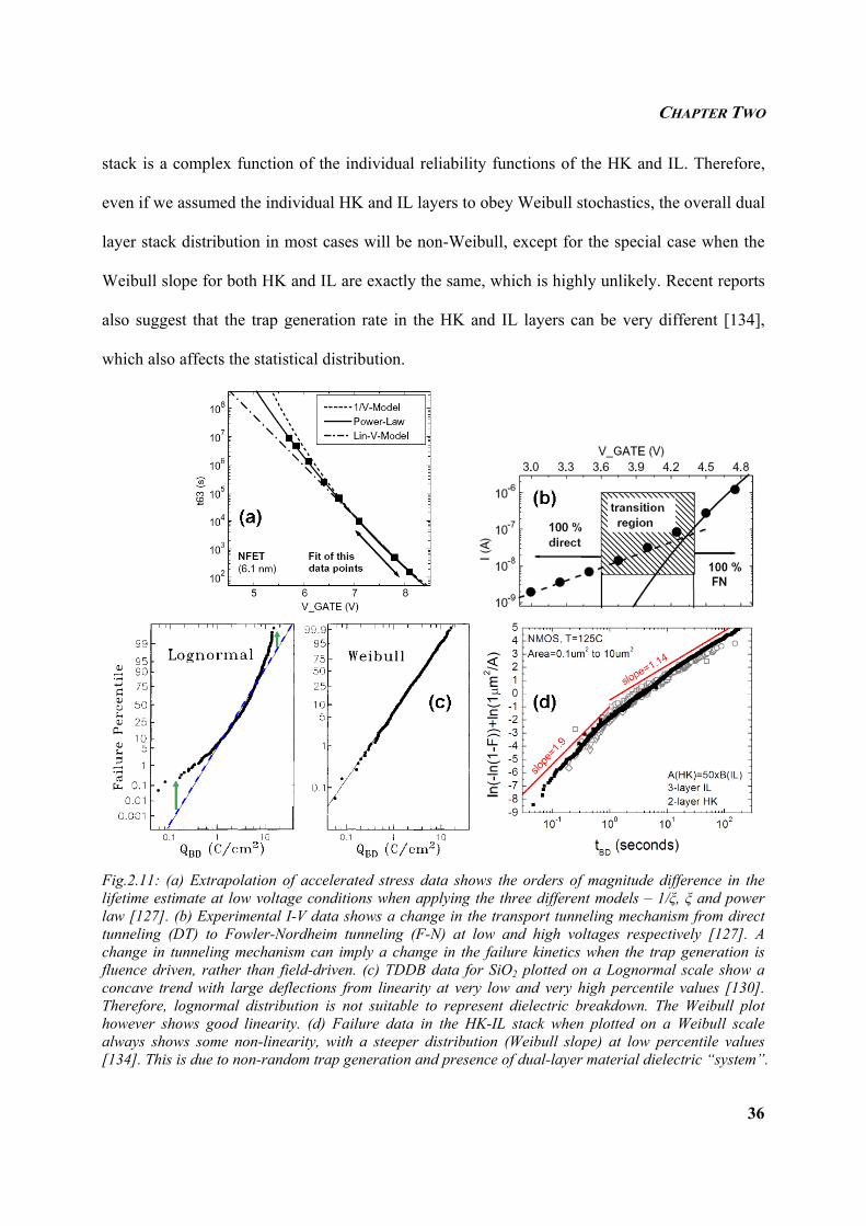
CHAPTER TWO
36
stack is a complex function of the individual reliability functions of the HK and IL. Therefore,
even if we assumed the individual HK and IL layers to obey Weibull stochastics, the overall dual
layer stack distribution in most cases will be non-Weibull, except for the special case when the
Weibull slope for both HK and IL are exactly the same, which is highly unlikely. Recent reports
also suggest that the trap generation rate in the HK and IL layers can be very different [134],
which also affects the statistical distribution.
Fig.2.11: (a) Extrapolation of accelerated stress data shows the orders of magnitude difference in the lifetime estimate at low voltage conditions when applying the three different models – 1/ξ, ξ and power law [127]. (b) Experimental I-V data shows a change in the transport tunneling mechanism from direct tunneling (DT) to Fowler-Nordheim tunneling (F-N) at low and high voltages respectively [127]. A change in tunneling mechanism can imply a change in the failure kinetics when the trap generation is fluence driven, rather than field-driven. (c) TDDB data for SiO2 plotted on a Lognormal scale show a concave trend with large deflections from linearity at very low and very high percentile values [130]. Therefore, lognormal distribution is not suitable to represent dielectric breakdown. The Weibull plot however shows good linearity. (d) Failure data in the HK-IL stack when plotted on a Weibull scale always shows some non-linearity, with a steeper distribution (Weibull slope) at low percentile values [134]. This is due to non-random trap generation and presence of dual-layer material dielectric “system”.
CHAPTER TWO
37
Considering the above factors, it is necessary for us to investigate how much deviation we
may observe from the standard Weibull trend in HK-IL stacks. We also need to find a solution as
to how we extrapolate our TTF data for non-Weibull conditions and whether there are any other
standard distributions that may describe the failure trends better. If Weibull should still be the
distribution of choice, is it valid for representing the low percentile range which is the region of
interest for integrated circuit reliability assessment? These are questions that we will deal with in
Chapter 4.
2.2.4 PHYSICAL FAILURE ANALYSIS
All this while, we have been mentioning time and again that dielectric BD is initiated by the
random generation of traps or defects across the oxide and a certain combination of these defects
cluster up to form a percolation path resulting in a catastrophic BD and low resistivity path for
high gate leakage current and power dissipation. The concept of trap / defect is speculative and
the exact physical / chemical nature of this “trap” needs to be identified. This requires the use of
various failure analysis tools such as HRTEM for imaging the device at a resolution of a few
angstroms, electron energy loss spectroscopy (EELS) for elemental mapping of oxygen and other
lighter elements, energy dispersive X-ray spectroscopy (EDX) for mapping heavy elements such
as Ti, Ta, Hf etc… and STM / conductive atomic force microscopy (CAFM) to probe the leakage
(tunneling) current magnitude of very small regions of size ~ 1 nm2 on blanket dielectric films.
All these tools and techniques can be used to our advantage in understanding the chemistry of
dielectric breakdown.
2.2.4.1 ROLE OF OXYGEN VACANCIES
A recent breakdown study by X. Li et. al. [135, 136] using the EELS technique on poly-Si –
SiON based gate stack was a major breakthrough in identifying oxygen vacancies (denoted as V0)
CHAPTER TWO
38
to be the primary form of the trap (defect). Prior to this, there were different explanations for
traps with some suggesting it to be an “electronic” trap in the band diagram based on quantum
physics interpretations and some postulating it to be “oxygen vacancies”. It was the work by X.
Li et. al. [135, 136] that helped clarify this issue using robust physical analysis results (Fig.
2.12(a, b)). It is now widely accepted that when the oxide is stressed, the Si-O bonds can be
broken by the influence of the applied electric field and/or energetic carriers (fluence) injected
into the oxide due to tunneling. While the cause of V0 generation is still being debated (whether it
is voltage induced, E-field induced or charge fluence induced) [137], the final effect is the
breakage of the Si-O bond and formation of the so-called E’-centers [138], which is an oxygen
vacancy configuration in the bulk of the dielectric. The dissociated oxygen (in the form of O2-) is
probably driven to the gate / substrate depending on the applied voltage polarity (inversion /
accumulation in NMOS / PMOS). In contrast, the Si-H bonds broken at the Si-SiON interface
are referred to as interface defects and denoted as “Pb-centers” [139]. Similarly, in HK dielectric
stacks as well, the oxygen vacancies are the functional form of the traps [140] and are formed by
breakage of the Hf-O bonds. The rate of trap generation is believed to be different in the HK and
SiON because of the different bonds (Si-O, Hf-O) being broken, each having its own
endothermic bond dissociation energy and activation energy barrier.
2.2.4.2 SIZE OF PERCOLATION PATH
Based on the EELS analysis results in Refs. [135, 136], the percolation path is basically an
oxygen-deficient region. The size and shape of this oxygen-deficient region has also been studied
using the same EELS technique and it is found that the percolation path is approximately
cylindrical in shape with a diameter of size 20-60 nm depending on the “hardness” of the BD
event [116, 141], which is in turn dependent on the compliance (Igl) used for TDDB. The
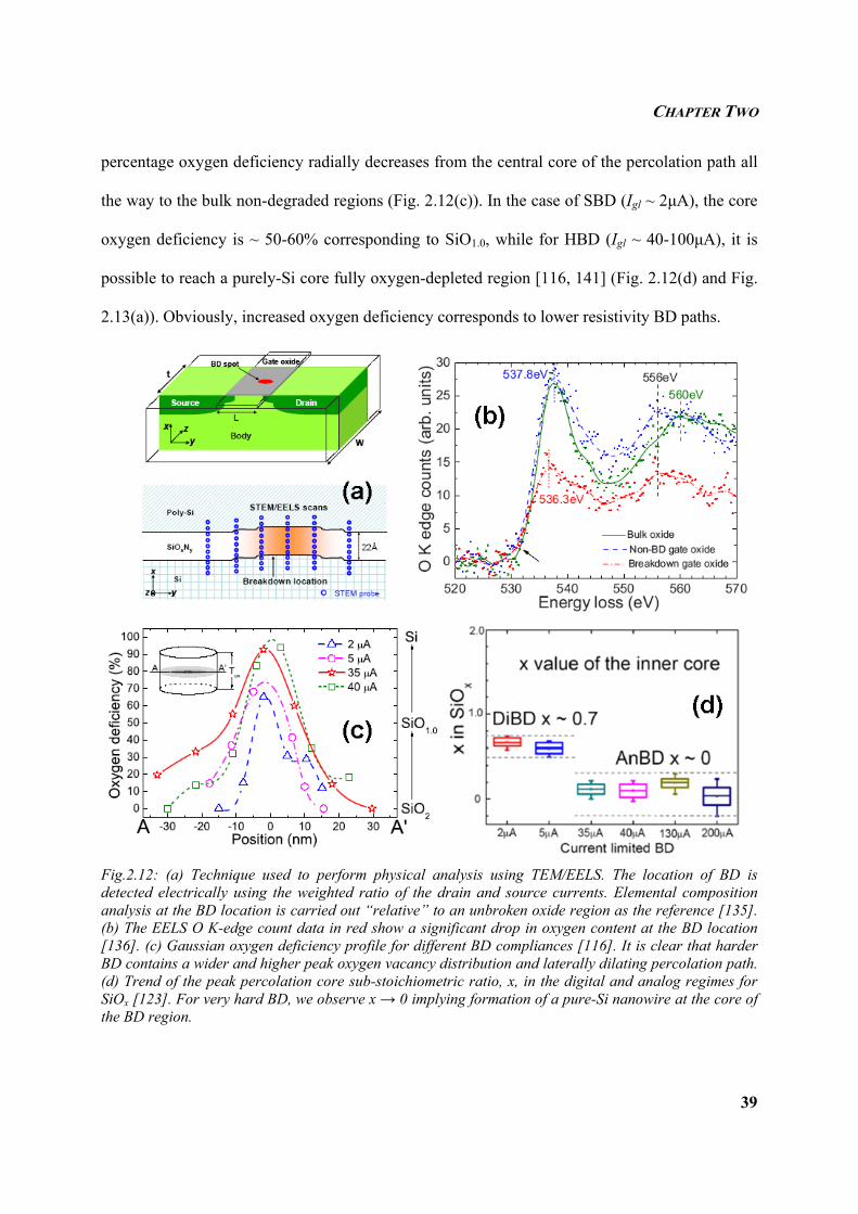
CHAPTER TWO
39
percentage oxygen deficiency radially decreases from the central core of the percolation path all
the way to the bulk non-degraded regions (Fig. 2.12(c)). In the case of SBD (Igl ~ 2µA), the core
oxygen deficiency is ~ 50-60% corresponding to SiO1.0, while for HBD (Igl ~ 40-100µA), it is
possible to reach a purely-Si core fully oxygen-depleted region [116, 141] (Fig. 2.12(d) and Fig.
2.13(a)). Obviously, increased oxygen deficiency corresponds to lower resistivity BD paths.
Fig.2.12: (a) Technique used to perform physical analysis using TEM/EELS. The location of BD is detected electrically using the weighted ratio of the drain and source currents. Elemental composition analysis at the BD location is carried out “relative” to an unbroken oxide region as the reference [135]. (b) The EELS O K-edge count data in red show a significant drop in oxygen content at the BD location [136]. (c) Gaussian oxygen deficiency profile for different BD compliances [116]. It is clear that harder BD contains a wider and higher peak oxygen vacancy distribution and laterally dilating percolation path. (d) Trend of the peak percolation core sub-stoichiometric ratio, x, in the digital and analog regimes for SiOx [123]. For very hard BD, we observe x → 0 implying formation of a pure-Si nanowire at the core of the BD region.
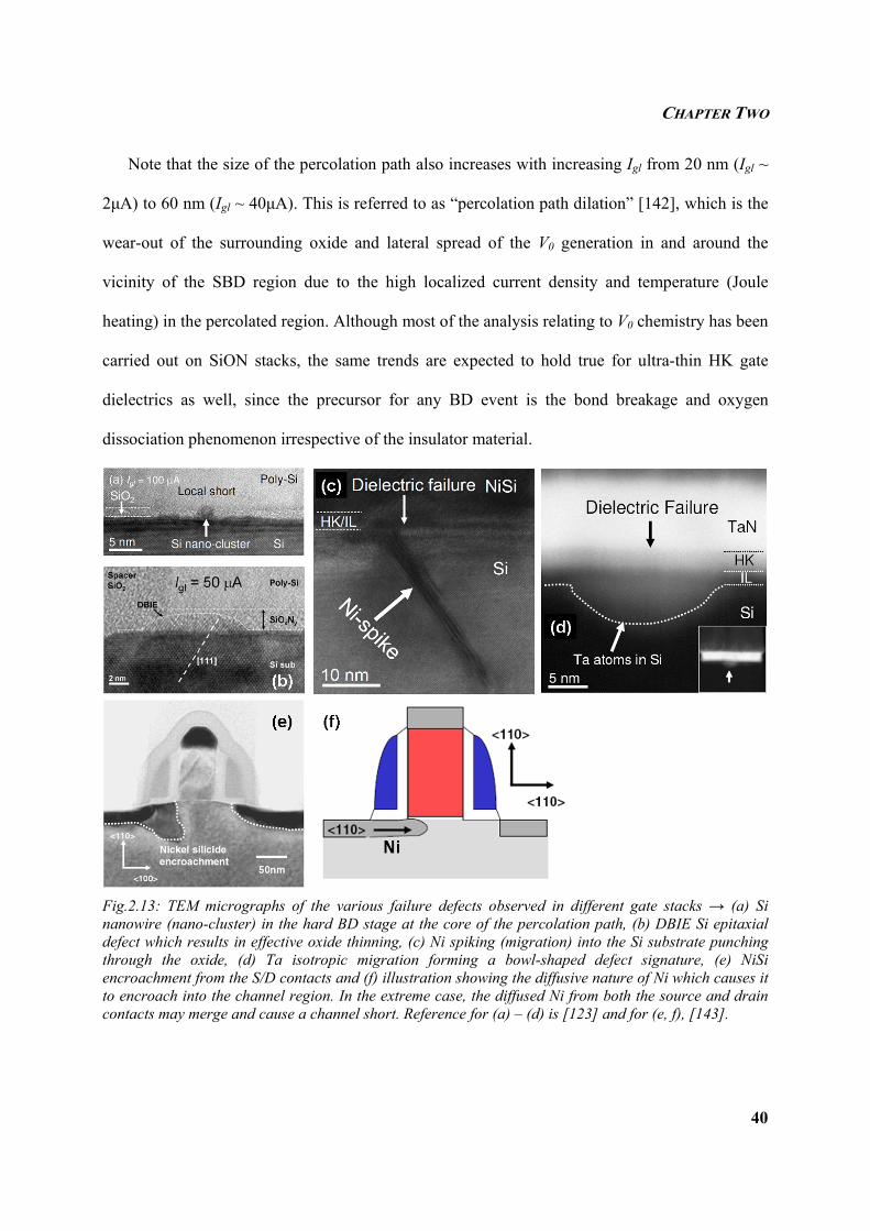
CHAPTER TWO
40
Note that the size of the percolation path also increases with increasing Igl from 20 nm (Igl ~
2µA) to 60 nm (Igl ~ 40µA). This is referred to as “percolation path dilation” [142], which is the
wear-out of the surrounding oxide and lateral spread of the V0 generation in and around the
vicinity of the SBD region due to the high localized current density and temperature (Joule
heating) in the percolated region. Although most of the analysis relating to V0 chemistry has been
carried out on SiON stacks, the same trends are expected to hold true for ultra-thin HK gate
dielectrics as well, since the precursor for any BD event is the bond breakage and oxygen
dissociation phenomenon irrespective of the insulator material.
Fig.2.13: TEM micrographs of the various failure defects observed in different gate stacks → (a) Si nanowire (nano-cluster) in the hard BD stage at the core of the percolation path, (b) DBIE Si epitaxial defect which results in effective oxide thinning, (c) Ni spiking (migration) into the Si substrate punching through the oxide, (d) Ta isotropic migration forming a bowl-shaped defect signature, (e) NiSi encroachment from the S/D contacts and (f) illustration showing the diffusive nature of Ni which causes it to encroach into the channel region. In the extreme case, the diffused Ni from both the source and drain contacts may merge and cause a channel short. Reference for (a) – (d) is [123] and for (e, f), [143].
CHAPTER TWO
41
2.2.4.3 DIELECTRIC BREAKDOWN INDUCED EPITAXY
In addition to the oxygen vacancy defects which required chemical detection using EELS,
physical changes in the microstructure / morphology were also observed in the transistor after
dielectric BD. One of the physical signatures observed consistently in many devices for both
SiON and HK based stacks was the inward protrusion / bulging of the substrate interface with the
oxide at the BD location. The silicon atoms from the substrate seem to have been collectively
pushed into the oxide at the BD spot making the oxide effectively thinner. This defect was called
as the “dielectric breakdown induced epitaxy (DBIE)” [40] (Fig. 2.13(b)) and the plausible
reason for this defect evolution is the current density induced electron wind force that causes Si
atoms to undergo thermomigration [115] (similar in analogy to the electromigration in Al and Cu
interconnects) at the high localized temperatures ~ 800-10000C in the percolation path. Although
silicon is more resistant to such migration, the high current density (which can go up to 4-40
MA/cm2) and temperature in the localized BD region can be sufficient to cause thermomigration
to occur.
The evolution of the DBIE defect happens through a positive feedback process wherein high
current density and temperature cause Si to migrate into the oxide, which reduces the effective
oxide thickness thereby increasing the current and Joule heating temperature further and so on.
Note however that while V0 defects can nucleate at any stage of transistor device operation,
nucleation of the DBIE defect requires a minimum BD compliance (hardness) of ~ 5µA [35]. At
lower compliance values, the driving force of current and temperature is insufficient to cause any
significant Si movement. The phenomenon of DBIE has been observed and confirmed in the
industry by Toshiba Corporation® [144].
CHAPTER TWO
42
2.2.4.4 METAL FILAMENTATION
While DBIE is a universal defect observed across all generations of gate stacks using the Si
as a substrate, an additional failure mechanism is observed in metal gate (NiSi, TiN, TaN) stacks
which involves migration of the metal spiking or punching through into the oxide causing an
ohmic metallic short between the gate and channel. This process is referred to as filamentation
[145] and it has been observed in Ni [146] (Fig. 2.13(c)) and Ta-based [62] (Fig. 2.13(d)) stacks
under HRTEM. The migrated material is confirmed to originate from the gate electrode using
EELS / EDX analysis as well. This filamentation phenomenon is observed in the post-BD stage
only for Igl > 5µA. The tendency for metal atoms to diffuse / migrate is postulated to be due to
ionic migration and/or hole migration as the direction of metallic transport is opposite to the
direction of electron flow (considering the NMOS transistor in inversion – substrate injection)
[62]. The presence of filaments is very detrimental to the post-BD reliability margin for
advanced MG-HK stacks as it tends to shorten or eliminate the digital fluctuation low current
regime observed immediately after TDDB in poly-Si based gate stacks. There is no analog
gradual wear-out observed in metal gated NMOS devices. Of the different metal electrodes
explored for the gate, Ni is the most diffusive and there are many reports which show Ni tending
to diffuse even before device stress during the high temperature (400-6000C) annealing stage of
the CMOS process [61, 147, 148]. While Ni tends to “spike” through the oxide preferentially in
the Si-[111] direction with a small filament size of ~ 2 nm [146], Ta migration appears to be
more isotropic with a larger filament size of ~ 10-15 nm [62].
2.2.4.5 DIELECTRIC BREAKDOWN INDUCED METAL MIGRATION
Similar to the migration of metal from the gate electrode into the oxide, another path of
migration originates from the silicide contacts of the source and drain ends. TEM micrographs
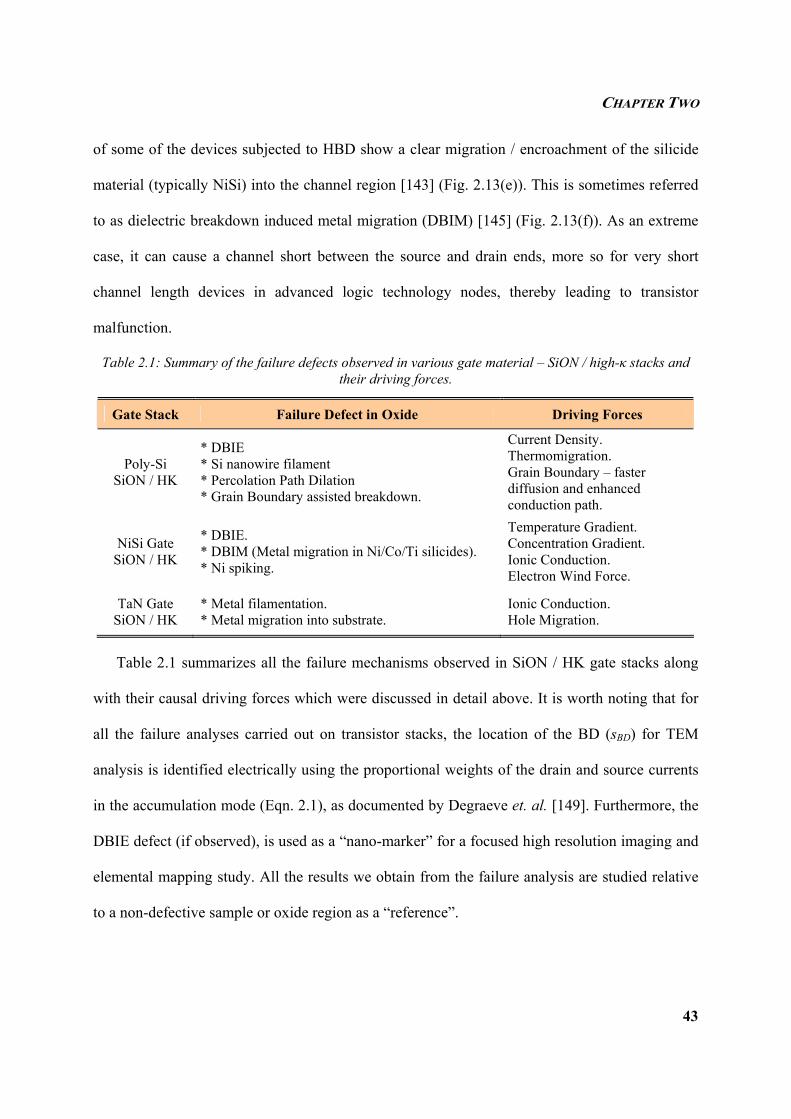
CHAPTER TWO
43
of some of the devices subjected to HBD show a clear migration / encroachment of the silicide
material (typically NiSi) into the channel region [143] (Fig. 2.13(e)). This is sometimes referred
to as dielectric breakdown induced metal migration (DBIM) [145] (Fig. 2.13(f)). As an extreme
case, it can cause a channel short between the source and drain ends, more so for very short
channel length devices in advanced logic technology nodes, thereby leading to transistor
malfunction.
Table 2.1: Summary of the failure defects observed in various gate material – SiON / high-κ stacks and their driving forces.
Gate Stack Failure Defect in Oxide Driving Forces
Poly-Si SiON / HK
* DBIE * Si nanowire filament * Percolation Path Dilation * Grain Boundary assisted breakdown.
Current Density. Thermomigration. Grain Boundary – faster diffusion and enhanced conduction path.
NiSi Gate SiON / HK
* DBIE. * DBIM (Metal migration in Ni/Co/Ti silicides). * Ni spiking.
Temperature Gradient. Concentration Gradient. Ionic Conduction. Electron Wind Force.
TaN Gate SiON / HK
* Metal filamentation. * Metal migration into substrate.
Ionic Conduction. Hole Migration.
Table 2.1 summarizes all the failure mechanisms observed in SiON / HK gate stacks along
with their causal driving forces which were discussed in detail above. It is worth noting that for
all the failure analyses carried out on transistor stacks, the location of the BD (sBD) for TEM
analysis is identified electrically using the proportional weights of the drain and source currents
in the accumulation mode (Eqn. 2.1), as documented by Degraeve et. al. [149]. Furthermore, the
DBIE defect (if observed), is used as a “nano-marker” for a focused high resolution imaging and
elemental mapping study. All the results we obtain from the failure analysis are studied relative
to a non-defective sample or oxide region as a “reference”.
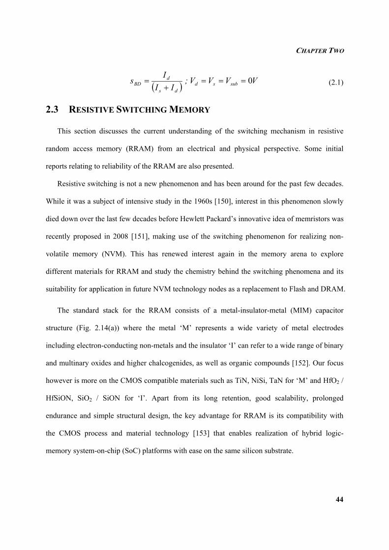
CHAPTER TWO
44
( ) VVVV;II
Is subsd
ds
dBD 0===
+= (2.1)
2.3 RESISTIVE SWITCHING MEMORY
This section discusses the current understanding of the switching mechanism in resistive
random access memory (RRAM) from an electrical and physical perspective. Some initial
reports relating to reliability of the RRAM are also presented.
Resistive switching is not a new phenomenon and has been around for the past few decades.
While it was a subject of intensive study in the 1960s [150], interest in this phenomenon slowly
died down over the last few decades before Hewlett Packard’s innovative idea of memristors was
recently proposed in 2008 [151], making use of the switching phenomenon for realizing non-
volatile memory (NVM). This has renewed interest again in the memory arena to explore
different materials for RRAM and study the chemistry behind the switching phenomena and its
suitability for application in future NVM technology nodes as a replacement to Flash and DRAM.
The standard stack for the RRAM consists of a metal-insulator-metal (MIM) capacitor
structure (Fig. 2.14(a)) where the metal ‘M’ represents a wide variety of metal electrodes
including electron-conducting non-metals and the insulator ‘I’ can refer to a wide range of binary
and multinary oxides and higher chalcogenides, as well as organic compounds [152]. Our focus
however is more on the CMOS compatible materials such as TiN, NiSi, TaN for ‘M’ and HfO2 /
HfSiON, SiO2 / SiON for ‘I’. Apart from its long retention, good scalability, prolonged
endurance and simple structural design, the key advantage for RRAM is its compatibility with
the CMOS process and material technology [153] that enables realization of hybrid logic-
memory system-on-chip (SoC) platforms with ease on the same silicon substrate.
CHAPTER TWO
45
2.3.1 ELECTRICAL CHARACTERIZATION
There are two types of switching that have been reported for an RRAM – unipolar and
bipolar. Unipolar switching refers to the same voltage polarity being used to initiate both the
SET (including Forming) and RESET events (Fig. 2.14(b)). In contrast, the bipolar switching
involves application of opposite polarities of voltage for the SET and RESET (Fig. 2.14(c)).
There is a third type of switching referred to as “non-polar” in which any polarity can be used to
cause switching for both SET and RESET. The term “SET” (and “Forming”) here refers to the
transition from the high (HRS) to low resistance state (LRS) analogous to a dielectric breakdown
event, while “RESET” is the vice-versa. There are various mechanisms proposed to explain the
switching phenomenon which include oxygen ion / oxygen vacancy transport [154, 155], metal
filament nucleation and rupture [156], electrochemical redox reactions [157] and electron
trapping / detrapping [158]. However, there is no concrete proof available to support any of these
and there is no single accepted phenomenon for switching. The mechanism is also expected to
depend very much on the materials used for the top/bottom electrode and the insulator.
Fig.2.14: (a) Schematic of the simple RRAM structure which is an M-I-M capacitor stack. I-V trends illustrating the (b) unipolar and (c) bipolar modes of switching [159].
The electrical characterization tests for RRAM include repeated I-V switching trends
showing the SET and RESET, retention analysis, endurance analysis, switching speed tests using
high frequency pulses and low voltage analysis to probe the read disturb immunity (RDI). In
CHAPTER TWO
46
Chapter 5, we will discuss how our observations of repeated breakdown and recovery in the
conventional MOSFET helped us understand and draw an analogy to the switching mechanism
governing the operation of RRAM. We will then discuss the switching mechanisms in detail in
Chapter 6 based on multiple polarity electrical characterization at different compliance levels for
the forming / SET transition.
2.3.2 RELIABILITY METRICS FOR SWITCHING MEMORY
In RRAM operation, reliability broadly encompasses the retention lifetime at the LRS and
HRS, number of endurance cycles that the device can sustain with sufficient memory window
and the read disturb immunity at low voltage. While very good endurance has been shown in
various reports [160], the analysis relating to retention lifetime is still very empirical [161, 162]
and very few reports exist which provide some insight based on phenomenological models [163].
There are cases wherein the retention is tested only for a duration of 10,000 seconds and this is
considered as a sufficient evidence to claim that the memory state can last for as long as 10 years
[164], which is the standard reliability requirement. This is however not acceptable because
retention loss is not a “gradual degradation” process that can be extended (extrapolated) from
short time resistance measurement data. It is a “catastrophic” phenomenon that needs to be
modeled based on the physics governing it. The added complication for retention analysis is that
the physical model to be proposed will depend on the mechanism of switching postulated. It is
therefore imperative to work on presenting a statistical and physical model (coherent with the
confirmed mechanism governing the switching process) that can accurately quantify the
retention lifetime expected from RRAM devices. This will be our main objective in Chapter 7,
wherein we take a statistical and thermodynamic perspective to study the retention criterion. We
will also briefly touch upon the read disturb immunity for the different resistance states.
CHAPTER TWO
47
2.3.3 PHYSICAL ANALYSIS OF SWITCHING MECHANISM
The best approach to find out the chemical nature of the switching process is to use the same
set of physical analysis tools listed in Section 2.2.4 for both the LRS and HRS states. This is
however easier said than done because currently investigated RRAM devices tend to be very
large in area ~ 10-100 µm2. Locating the filament is an arduous task in such large area devices
and considering that the device is an MIM capacitor (not a transistor), there are no electrical
means to identifying the filament location. Therefore, it is purely by chance that any basic insight
on the filament can be gained in a typical MIM stack. However, there are a few studies which
have managed to unearth some details on the filament nature using TEM [165], scanning
electron microscopy (SEM) [166] and STM analysis [167] tools.
A very effective approach has been adopted recently by our group wherein we use the M-I-S
transistor as a test structure for RRAM. The transistor structure helps identify the location of the
filament (using Eqn. (2.1)) along the channel of the device after BD (SET). As a result, it is
easier to locate the filament and probe its chemical nature. Various devices were subjected to the
forming stage with different compliance values. For Igl < 5µA, no physical defects were found,
however EELS analysis clearly indicated regions of high oxygen deficiency. For the case of Igl
>> 5µA, metal filaments were clearly observed in Ni electrode based stacks [146]. This tends to
suggest that the mechanism of switching may be very much compliance dependent. We hope to
verify the claim of compliance dependent switching mechanism using an electrical
characterization setup in Chapter 6. It is worth noting that our use of the M-I-S stack for
understanding resistive switching was motivated by the post breakdown recovery in leakage
current that we consistently observed in the transistor [168], which was analogous to the RESET
phenomenon in RRAM.
CHAPTER TWO
48
2.4 SUMMARY
We have presented a detailed literature review on the results achieved in the areas of high-κ
logic reliability and resistive switching. Based on the review presented, we have been able to
identify the issues relating to HK logic reliability that deserve in-depth investigations. This
includes the need to decipher the sequence of BD, model the reliability statistics in a dual layer
dielectric stack and understanding the role of the grain boundary on the TDDB Weibull
distribution. Similarly, we have identified the need to understand the chemistry of switching in
RRAM from an electrical perspective, making use of the M-I-S logic transistor as an effective
test structure. The following chapters will deal with all these objectives. In Chapter 3, we shall
first use electrical characterization techniques to probe the physics of BD in the dual layer HK-IL
gate stacks.
CHAPTER THREE
49
CHAPTER THREE
EEELLLEEECCCTTTRRRIIICCCAAALLL CCCHHHAAARRRAAACCCTTTEEERRRIIIZZZAAATTTIIIOOONNN OOOFFF HHHIIIGGGHHH---KKK
IIINNNTTTEEERRRFFFAAACCCIIIAAALLL LLLAAAYYYEEERRR BBBRRREEEAAAKKKDDDOOOWWWNNN
3.1 INTRODUCTION
As discussed in the literature review, one of the key tasks is to decipher the sequence of
breakdown in a dual layer high-κ - interfacial layer dielectric stack. In order to study this, it is
necessary to develop a suitable electrical test algorithm and use various analytical techniques to
help identify the first layer that breaks down. The main objective of this chapter is to deal with
this important topic. Towards the later part of this chapter, we will also discuss the post-BD
reliability and robustness of the gate stack and make inferences on whether the dual layer
dielectric is immune to the analog wear-out process or not.
3.2 EXPERIMENTAL SETUP
The setup for our electrical characterization and measurements include the SUSS® Microtech
8-inch wafer probe station along with the Keithley SCS-4200 precision semiconductor parameter
analyzer (Fig. 3.1). The probe station consists of a thermo chuck and the heater can be set to a
wide range of temperature stresses ranging from 250C – 2000C. The parameter analyzer consists
of four highly accurate source-measurement units (SMUs) with two of them connected to a pre-
amplifier so as to be able to achieve femto-ampere (fA) range resolution of current measurement.
The SMU connected with the pre-amp is used for measurement of gate leakage current,
considering its high sensitivity to small fluctuations and ability to measure very low currents.
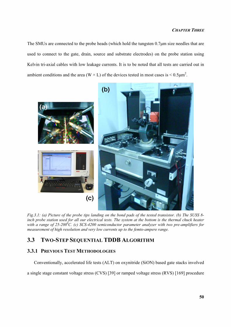
CHAPTER THREE
50
The SMUs are connected to the probe heads (which hold the tungsten 0.7µm size needles that are
used to connect to the gate, drain, source and substrate electrodes) on the probe station using
Kelvin tri-axial cables with low leakage currents. It is to be noted that all tests are carried out in
ambient conditions and the area (W × L) of the devices tested in most cases is < 0.5µm2.
Fig.3.1: (a) Picture of the probe tips landing on the bond pads of the tested transistor. (b) The SUSS 8-inch probe station used for all our electrical tests. The system at the bottom is the thermal chuck heater with a range of 25-2000C. (c) SCS-4200 semiconductor parameter analyzer with two pre-amplifiers for measurement of high resolution and very low currents up to the femto-ampere range.
3.3 TWO-STEP SEQUENTIAL TDDB ALGORITHM
3.3.1 PREVIOUS TEST METHODOLOGIES
Conventionally, accelerated life tests (ALT) on oxynitride (SiON) based gate stacks involved
a single stage constant voltage stress (CVS) [39] or ramped voltage stress (RVS) [169] procedure
CHAPTER THREE
51
with a high compliance value of around 50-100µA to initiate BD of the oxide. The corresponding
times to failure were recorded for many similar tested devices and then the standard Weibull
distribution model and extrapolation procedure was used to predict the field TDDB lifetime (Vg
= Vop = 1V) and Weibull slope. This simple procedure worked perfectly for SiON as the
dielectric comprised of just a single material film and as a result, the CVS stress level (as long as
Vg < VBD) and compliance setting (Igl) chosen were generally not very critical as long as a
catastrophic BD event (jump in Ig) was clearly observed in finite non-zero time.
However, for the case of a dual-layer HK-IL stack, if the same procedure above is applied,
the “intrinsic” reliability of the stack may not be assessable. This is because once the first layer
breaks down, the entire gate voltage stress ideally drops across the surviving second layer and it
is highly likely that the electric field across this layer may exceed its critical BD field strength
(ξBD) for typical accelerated stress conditions. As a result, breakdown of the second layer would
tend to be abrupt and instantaneous.
It is well known in TDDB test methodologies that the stress voltage should be at least about
0.5-0.7V lower than VBD, if the intrinsic reliability of the oxide is to be studied [170]. Most
previous studies on TDDB assessment [169, 171-173] for HK gate stacks followed the above
procedure of single stage CVS / RVS and hence the obtained lifetime estimates were erroneous.
Moreover, the use of this methodology does not allow us to decode the Weibull slope and
lifetime of the individual HK and IL layers. Considering the limitations of the conventional test,
we propose here a two-stage CVS methodology that successfully enables sequential BD of the
individual HK and IL layers without any abrupt complete stack BD. The algorithm is presented
in the next sub-section.
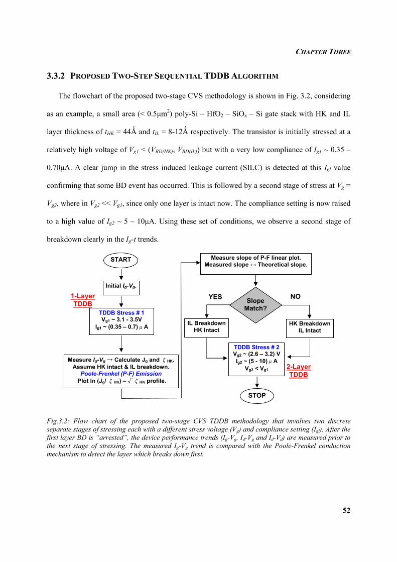
CHAPTER THREE
52
3.3.2 PROPOSED TWO-STEP SEQUENTIAL TDDB ALGORITHM
The flowchart of the proposed two-stage CVS methodology is shown in Fig. 3.2, considering
as an example, a small area (< 0.5µm2) poly-Si – HfO2 – SiOx – Si gate stack with HK and IL
layer thickness of tHK = 44Ǻ and tIL = 8-12Ǻ respectively. The transistor is initially stressed at a
relatively high voltage of Vg1 < (VBD(HK), VBD(IL)) but with a very low compliance of Ig1 ~ 0.35 –
0.70µA. A clear jump in the stress induced leakage current (SILC) is detected at this Igl value
confirming that some BD event has occurred. This is followed by a second stage of stress at Vg =
Vg2, where in Vg2 << Vg1, since only one layer is intact now. The compliance setting is now raised
to a high value of Ig2 ~ 5 – 10µA. Using these set of conditions, we observe a second stage of
breakdown clearly in the Ig-t trends.
Fig.3.2: Flow chart of the proposed two-stage CVS TDDB methodology that involves two discrete separate stages of stressing each with a different stress voltage (Vg) and compliance setting (Igl). After the first layer BD is “arrested”, the device performance trends (Ig-Vg, Id-Vg and Id-Vd) are measured prior to the next stage of stressing. The measured Ig-Vg trend is compared with the Poole-Frenkel conduction mechanism to detect the layer which breaks down first.
START
Initial Ig-Vg.
Measure slope of P-F linear plot. Measured slope ↔ Theoretical slope.
TDDB Stress # 1 Vg1 ~ 3.1 - 3.5V
Ig1 ~ (0.35 – 0.7)μA
TDDB Stress # 2Vg2 ~ (2.6 – 3.2) V Ig2 ~ (5 - 10)μA
Vg2 < Vg1 Measure Ig-Vg → Calculate Jg and ξHK.
Assume HK intact & IL breakdown. Poole-Frenkel (P-F) Emission
Plot ln (Jg/ ξHK) – √ξHK profile.
STOP
Slope Match?
YES
IL BreakdownHK Intact
HK BreakdownIL Intact
2-Layer TDDB
1-Layer TDDB
NO
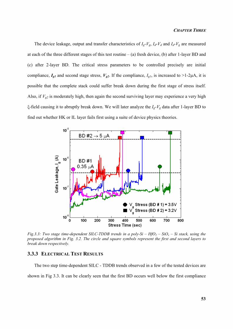
CHAPTER THREE
53
The device leakage, output and transfer characteristics of Ig-Vg, Id-Vd and Id-Vg are measured
at each of the three different stages of this test routine – (a) fresh device, (b) after 1-layer BD and
(c) after 2-layer BD. The critical stress parameters to be controlled precisely are initial
compliance, Ig1 and second stage stress, Vg2. If the compliance, Ig1, is increased to >1-2µA, it is
possible that the complete stack could suffer break down during the first stage of stress itself.
Also, if Vg2 is moderately high, then again the second surviving layer may experience a very high
ξ-field causing it to abruptly break down. We will later analyze the Ig-Vg data after 1-layer BD to
find out whether HK or IL layer fails first using a suite of device physics theories.
Fig.3.3: Two stage time-dependent SILC-TDDB trends in a poly-Si – HfO2 – SiOx – Si stack, using the proposed algorithm in Fig. 3.2. The circle and square symbols represent the first and second layers to break down respectively.
3.3.3 ELECTRICAL TEST RESULTS
The two step time-dependent SILC - TDDB trends observed in a few of the tested devices are
shown in Fig 3.3. It can be clearly seen that the first BD occurs well below the first compliance
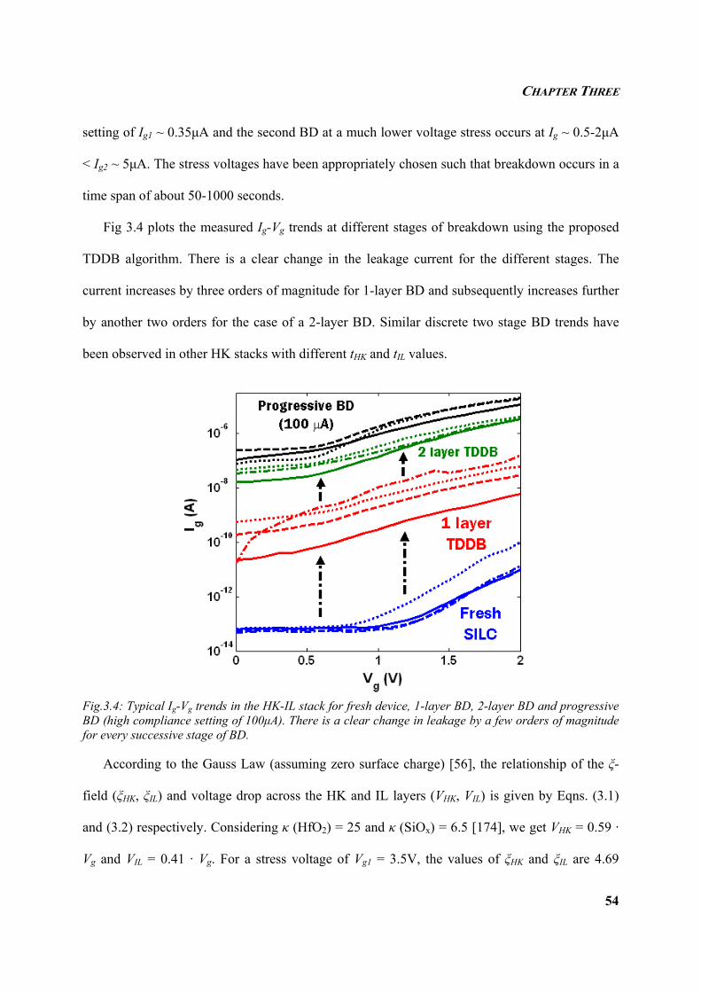
CHAPTER THREE
54
setting of Ig1 ~ 0.35µA and the second BD at a much lower voltage stress occurs at Ig ~ 0.5-2µA
< Ig2 ~ 5µA. The stress voltages have been appropriately chosen such that breakdown occurs in a
time span of about 50-1000 seconds.
Fig 3.4 plots the measured Ig-Vg trends at different stages of breakdown using the proposed
TDDB algorithm. There is a clear change in the leakage current for the different stages. The
current increases by three orders of magnitude for 1-layer BD and subsequently increases further
by another two orders for the case of a 2-layer BD. Similar discrete two stage BD trends have
been observed in other HK stacks with different tHK and tIL values.
Fig.3.4: Typical Ig-Vg trends in the HK-IL stack for fresh device, 1-layer BD, 2-layer BD and progressive BD (high compliance setting of 100µA). There is a clear change in leakage by a few orders of magnitude for every successive stage of BD.
According to the Gauss Law (assuming zero surface charge) [56], the relationship of the ξ-
field (ξHK, ξIL) and voltage drop across the HK and IL layers (VHK, VIL) is given by Eqns. (3.1)
and (3.2) respectively. Considering κ (HfO2) = 25 and κ (SiOx) = 6.5 [174], we get VHK = 0.59 ·
Vg and VIL = 0.41 · Vg. For a stress voltage of Vg1 = 3.5V, the values of ξHK and ξIL are 4.69
CHAPTER THREE
55
MV/cm and 11.95 MV/cm respectively, which is much lower than their critical BD field
strengths of 6 MV/cm for HfO2 and 15 MV/cm for SiO2 [93]. Therefore, the stress conditions we
use for TDDB test are such that the applied field across the HK and IL layers is much lower than
their critical field strength. For the second stage of stressing, since it takes non-zero time for
subsequent BD, we confirm that the critical BD field of the surviving dielectric layer (which
needs to be identified next) is not attained.
ILILHKHK ξκξκ = (3.1)
1
1−
⎟⎟⎠
⎞⎜⎜⎝
⎛+⋅⋅=
IL
IL
HK
HKgHK
tt
VVκ
κ (3.2)
3.4 DETECTION OF DUAL LAYER BREAKDOWN SEQUENCE
3.4.1 TECHNIQUES AND RESULTS IN THE PAST
While the algorithm in the previous section only enables us to “arrest” BD at the one layer-
BD stage and subsequently cause the second layer TDDB in “finite time”, the sequence in which
the dielectric layers degrade and break down is yet to be ascertained. The question to be
answered is: Does HK break down first or is it the IL? Moreover, which of them has a higher
trap generation rate? This sequence is an important pre-requisite for proper reliability modeling
and to decode the Weibull slope of the HK and IL layers. Without a proper identification of the
sequence, all inferences from experimental reliability tests will be redundant.
Various characterization techniques have been used in recent literature to try to decode the
sequence as summarized in Table 3.1 below. It can be seen that the results from different
research groups tend to conflict with each other and there is no single outcome agreed upon yet.
It is difficult to judge these results objectively as each of them are based on different approaches.
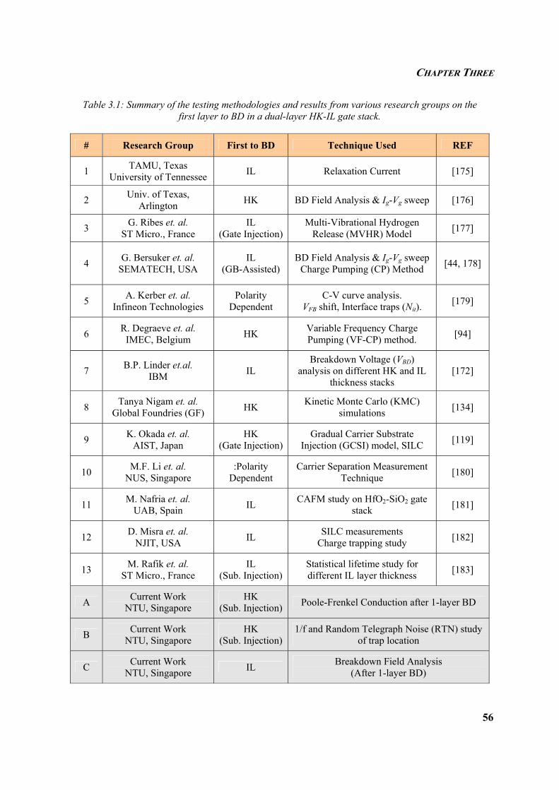
CHAPTER THREE
56
Table 3.1: Summary of the testing methodologies and results from various research groups on the first layer to BD in a dual-layer HK-IL gate stack.
# Research Group First to BD Technique Used REF
1 TAMU, Texas University of Tennessee IL Relaxation Current [175]
2 Univ. of Texas, Arlington HK BD Field Analysis & Ig-Vg sweep [176]
3 G. Ribes et. al. ST Micro., France
IL (Gate Injection)
Multi-Vibrational Hydrogen Release (MVHR) Model [177]
4 G. Bersuker et. al. SEMATECH, USA
IL (GB-Assisted)
BD Field Analysis & Ig-Vg sweep Charge Pumping (CP) Method [44, 178]
5 A. Kerber et. al. Infineon Technologies
Polarity Dependent
C-V curve analysis. VFB shift, Interface traps (Nit).
[179]
6 R. Degraeve et. al. IMEC, Belgium HK Variable Frequency Charge
Pumping (VF-CP) method. [94]
7 B.P. Linder et.al. IBM IL
Breakdown Voltage (VBD) analysis on different HK and IL
thickness stacks [172]
8 Tanya Nigam et. al. Global Foundries (GF) HK Kinetic Monte Carlo (KMC)
simulations [134]
9 K. Okada et. al. AIST, Japan
HK (Gate Injection)
Gradual Carrier Substrate Injection (GCSI) model, SILC [119]
10 M.F. Li et. al. NUS, Singapore
:Polarity Dependent
Carrier Separation Measurement Technique [180]
11 M. Nafria et. al. UAB, Spain IL CAFM study on HfO2-SiO2 gate
stack [181]
12 D. Misra et. al. NJIT, USA IL SILC measurements
Charge trapping study [182]
13 M. Rafik et. al. ST Micro., France
IL (Sub. Injection)
Statistical lifetime study for different IL layer thickness [183]
A Current Work NTU, Singapore
HK (Sub. Injection) Poole-Frenkel Conduction after 1-layer BD
B Current Work NTU, Singapore
HK (Sub. Injection)
1/f and Random Telegraph Noise (RTN) study of trap location
C Current Work NTU, Singapore IL Breakdown Field Analysis
(After 1-layer BD)
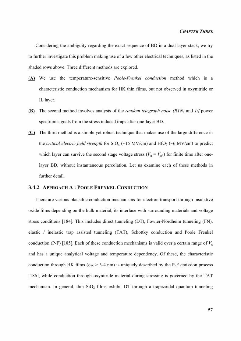
CHAPTER THREE
57
Considering the ambiguity regarding the exact sequence of BD in a dual layer stack, we try
to further investigate this problem making use of a few other electrical techniques, as listed in the
shaded rows above. Three different methods are explored.
(A) We use the temperature-sensitive Poole-Frenkel conduction method which is a
characteristic conduction mechanism for HK thin films, but not observed in oxynitride or
IL layer.
(B) The second method involves analysis of the random telegraph noise (RTN) and 1/f power
spectrum signals from the stress induced traps after one-layer BD.
(C) The third method is a simple yet robust technique that makes use of the large difference in
the critical electric field strength for SiOx (~15 MV/cm) and HfO2 (~6 MV/cm) to predict
which layer can survive the second stage voltage stress (Vg = Vg2) for finite time after one-
layer BD, without instantaneous percolation. Let us examine each of these methods in
further detail.
3.4.2 APPROACH A : POOLE FRENKEL CONDUCTION
There are various plausible conduction mechanisms for electron transport through insulative
oxide films depending on the bulk material, its interface with surrounding materials and voltage
stress conditions [184]. This includes direct tunneling (DT), Fowler-Nordheim tunneling (FN),
elastic / inelastic trap assisted tunneling (TAT), Schottky conduction and Poole Frenkel
conduction (P-F) [185]. Each of these conduction mechanisms is valid over a certain range of Vg
and has a unique analytical voltage and temperature dependency. Of these, the characteristic
conduction through HK films (tHK > 3-4 nm) is uniquely described by the P-F emission process
[186], while conduction through oxynitride material during stressing is governed by the TAT
mechanism. In general, thin SiO2 films exhibit DT through a trapezoidal quantum tunneling
CHAPTER THREE
58
barrier while thick films show FN tunneling through a triangular barrier. The P-F emission
involves thermally-assisted field emission of charge carriers across the trap potential wells.
Application of a field reduces the potential barrier for carrier transport (emission) across these
traps and thermal effects provide the activation energy for this conduction process, as illustrated
in Fig. 3.5 [56, 187].
Fig.3.5: Schematic showing the trapping and detrapping process of electron charge carriers at trap potential wells. The potential barrier is reduced by the applied electric field and carrier transport is thermally enhanced in this Poole-Frenkel conduction process, which is typical of high-κ dielectric thin films [187].
Let us now consider the case of a one-layer BD. As mentioned earlier, we measure the Ig-Vg
characteristics of the device at this stage. If we assume the IL layer to have broken down and
consider the dielectric BD region to be “purely resistive” (overlap of trap wavefunctions creates
a defect band in the bandgap), then the conduction through the intact HK – broken IL should
show P-F emission trends. On the contrary, if the HK has suffered a BD and the IL remains
intact, then the overall conduction through the stack is limited by the inelastic trap-assisted
tunneling (ITAT) mechanism which is typical of transport in stressed Si-O layers [188]. Since
the analytical formulation for the ITAT mechanism is more complex [189, 190], we employ the
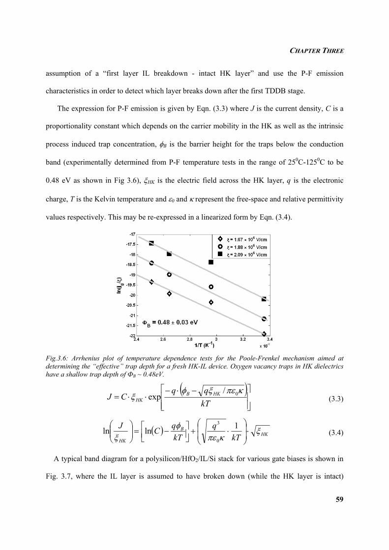
CHAPTER THREE
59
assumption of a “first layer IL breakdown - intact HK layer” and use the P-F emission
characteristics in order to detect which layer breaks down after the first TDDB stage.
The expression for P-F emission is given by Eqn. (3.3) where J is the current density, C is a
proportionality constant which depends on the carrier mobility in the HK as well as the intrinsic
process induced trap concentration, φB is the barrier height for the traps below the conduction
band (experimentally determined from P-F temperature tests in the range of 250C-1250C to be
0.48 eV as shown in Fig 3.6), ξHK is the electric field across the HK layer, q is the electronic
charge, T is the Kelvin temperature and ε0 and κ represent the free-space and relative permittivity
values respectively. This may be re-expressed in a linearized form by Eqn. (3.4).
Fig.3.6: Arrhenius plot of temperature dependence tests for the Poole-Frenkel mechanism aimed at determining the “effective” trap depth for a fresh HK-IL device. Oxygen vacancy traps in HK dielectrics have a shallow trap depth of ФB ~ 0.48eV.
( )⎥⎥⎦
⎤
⎢⎢⎣
⎡ −⋅−⋅⋅=
kTqq
CJ HKBHK
κπεξφξ 0/
exp (3.3)
( ) HKB
HK kTq
kTqCJ ξ
κπεφ
ξ⋅⎟⎟⎠
⎞⎜⎜⎝
⎛⋅+⎥⎦
⎤⎢⎣⎡ −=⎟⎟
⎠
⎞⎜⎜⎝
⎛ 1lnln0
3
(3.4)
A typical band diagram for a polysilicon/HfO2/IL/Si stack for various gate biases is shown in
Fig. 3.7, where the IL layer is assumed to have broken down (while the HK layer is intact)
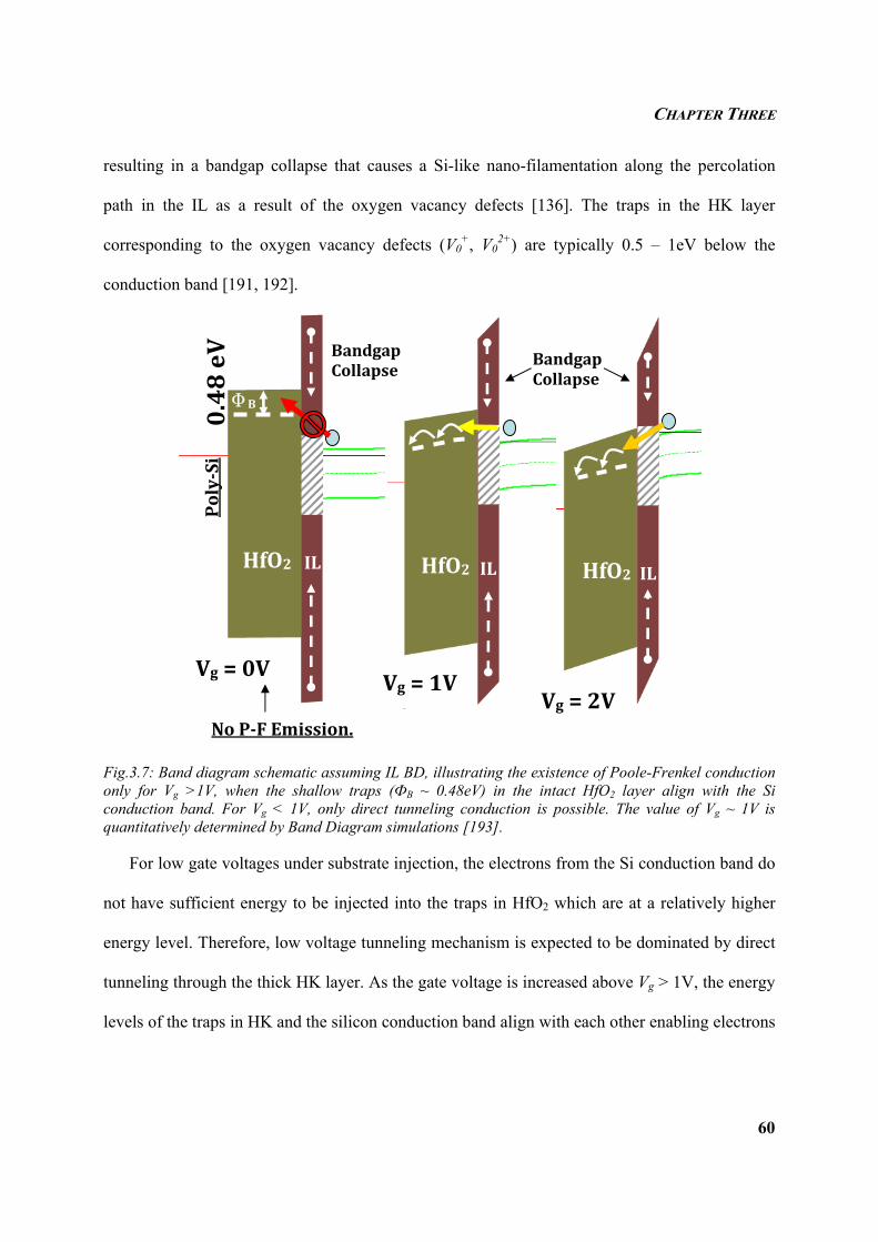
CHAPTER THREE
60
resulting in a bandgap collapse that causes a Si-like nano-filamentation along the percolation
path in the IL as a result of the oxygen vacancy defects [136]. The traps in the HK layer
corresponding to the oxygen vacancy defects (V0+, V0
2+) are typically 0.5 – 1eV below the
conduction band [191, 192].
Fig.3.7: Band diagram schematic assuming IL BD, illustrating the existence of Poole-Frenkel conduction only for Vg >1V, when the shallow traps (ФB ~ 0.48eV) in the intact HfO2 layer align with the Si conduction band. For Vg < 1V, only direct tunneling conduction is possible. The value of Vg ~ 1V is quantitatively determined by Band Diagram simulations [193].
For low gate voltages under substrate injection, the electrons from the Si conduction band do
not have sufficient energy to be injected into the traps in HfO2 which are at a relatively higher
energy level. Therefore, low voltage tunneling mechanism is expected to be dominated by direct
tunneling through the thick HK layer. As the gate voltage is increased above Vg > 1V, the energy
levels of the traps in HK and the silicon conduction band align with each other enabling electrons
HfO2 HfO2 HfO2
Pol
y-Si
IL IL IL
Vg = 0VVg = 1V
Vg = 2VNo P-F Emission.
Bandgap Collapse Bandgap
Collapse
0.4
8 e
V
ΦB
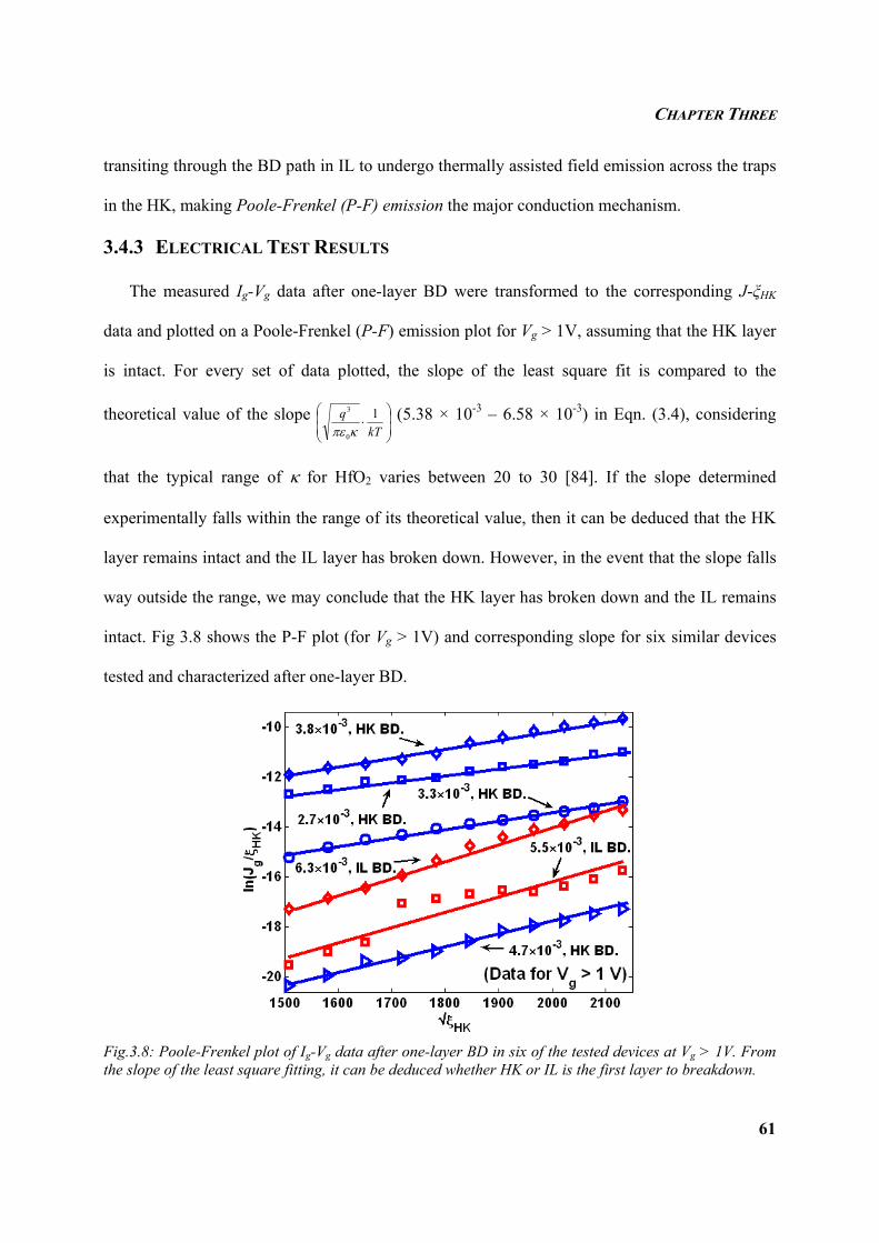
CHAPTER THREE
61
transiting through the BD path in IL to undergo thermally assisted field emission across the traps
in the HK, making Poole-Frenkel (P-F) emission the major conduction mechanism.
3.4.3 ELECTRICAL TEST RESULTS
The measured Ig-Vg data after one-layer BD were transformed to the corresponding J-ξHK
data and plotted on a Poole-Frenkel (P-F) emission plot for Vg > 1V, assuming that the HK layer
is intact. For every set of data plotted, the slope of the least square fit is compared to the
theoretical value of the slope ⎟⎟⎠
⎞⎜⎜⎝
⎛⋅kT
q 1
0
3
κπε (5.38 × 10⁻³ – 6.58 × 10⁻³) in Eqn. (3.4), considering
that the typical range of κ for HfO2 varies between 20 to 30 [84]. If the slope determined
experimentally falls within the range of its theoretical value, then it can be deduced that the HK
layer remains intact and the IL layer has broken down. However, in the event that the slope falls
way outside the range, we may conclude that the HK layer has broken down and the IL remains
intact. Fig 3.8 shows the P-F plot (for Vg > 1V) and corresponding slope for six similar devices
tested and characterized after one-layer BD.
Fig.3.8: Poole-Frenkel plot of Ig-Vg data after one-layer BD in six of the tested devices at Vg > 1V. From the slope of the least square fitting, it can be deduced whether HK or IL is the first layer to breakdown.
CHAPTER THREE
62
A total of 36 devices were tested using the two-step TDDB algorithm and the same P-F
analysis was carried out. Of these, 31 devices (~ 85%) had a slope well outside of the theoretical
range (5.38 × 10⁻³ – 6.58 × 10⁻³) implying that HK is the first layer to BD. Only around 5 devices
were indicative of IL failure. Assuming our methodology above to be valid, we may suggest that
for NMOS devices in substrate injection mode, HK is generally the first layer to suffer BD.
It is important to note that the proposed method above lies on one key assumption. We
assume that the layer which suffers a soft BD can be represented as a simple ‘ohmic’ resistor
after percolation. However, some recent studies [194, 195] have shown that a purely resistive
model is not applicable even in the complete bi-layer post-BD stage. Instead, the post-BD trends
in gate dielectrics are better described by a diode model [194] or quantum point contact (QPC)
model [195], in which case, the conclusions of our study above need to be reassessed.
3.4.4 APPROACH B : 1/F NOISE AND RTN STUDY
The second approach we use to identify the sequence of BD is by analyzing the time domain
random telegraph noise (RTN) fluctuations and frequency domain power spectra of the gate
current (Ig) in the device after one-layer BD. The origin of RTN is the stochastic capture and
emission of electrons at the oxygen vacancy traps (both process and stress induced). According
to noise theory [196] in nanodevices, there are three primary sources of noise with different
exponents in the power spectral density (PSD) plot – (A) 1/f0 component – white noise, also
called shot noise / thermal noise, (B) 1/f1 component – pink noise, due to generation-
recombination (G-R) of electron hole pairs and (C) 1/f2 component – due to RTN signals at
discrete current levels, also called Brownian noise. Given any signal of Ig fluctuation at low
sense voltage, the exponent of the PSD spectrum (α) indicates the relative dominance of the
different noise sources. When α → 1, G-R component is dominant; α → 2 implies digital current
CHAPTER THREE
63
fluctuations from traps and α → 0 indicates thermal or shot noise effects. The PSD information is
obtained by taking a Fast Fourier Transform (FFT) [197] of the time domain Ig data. For
comparison purposes, we analyze the RTN and 1/f information for all the three different stages of
BD and four possible scenarios → (A) fresh device, (B) one layer HK BD, (C) one layer IL BD
and (D) bi-layer complete stack BD.
Very low sense voltage stress of Vg ~ 1.0-1.5V is applied to extract the Ig-RTN signals (Vd =
Vs = Vsub = 0V) that represent the kinetics of electron trapping and detrapping events using the
Keithley SCS-4200 system, where the gate source measurement unit (SMU) is connected to a
low-noise pre-amplifier capable of measuring currents up to the femto-ampere (fA) range. We
intentionally make use of a 10ms low time resolution probing system here to distinguish the
trap/detrap behavior and noise signals from the HK and IL layer traps. The gate current noise
(SIg(f)) is analyzed instead of the drain current noise (SId(f)) in this study, as the gate fluctuations
describe the collective behavior of the bulk HK and IL traps while drain current fluctuations only
provide information on interface and near-interface traps, as reported by Giusi et. al. [198].
The time constant for the trapping / detrapping process extracted from time domain RTN
signals can be used to estimate the location of traps in the dielectric, based on various tunneling
models developed [196]. Here, we use the simple elastic tunneling model to find out the location
of the traps from the RTN measurements after one-layer BD.
The four possible scenarios (or cases) of device operation for the bi-layer HK/IL stack are
illustrated in Fig 3.9. Case A refers to a fresh device with isolated process induced traps (PIT) in
the HK and a supposedly defect-free IL layer, which is generally the case [199]. Here, Ig would
involve many independent uncorrelated trap-assisted-tunneling (TAT) events. Depending on the
vertical location (z) of the trap with reference to the substrate, the time constant (τ) for the carrier
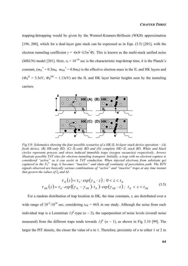
CHAPTER THREE
64
trapping/detrapping would be given by the Wentzel-Kramers-Brillouin (WKB) approximation
[196, 200], which for a dual-layer gate stack can be expressed as in Eqn. (3.5) [201], with the
electron tunneling coefficient γ = 4π/h·√(2m*Ф). This is known as the multi-stack unified noise
(MSUN) model [201]. Here, τ0 = 10-10 sec is the characteristic trap/detrap time, h is the Planck’s
constant, (mIL* = 0.3m0, mHK
* = 0.8m0) is the effective electron mass in the IL and HK layers and
(ФBIL = 3.5eV, ФB
HK = 1.13eV) are the IL and HK layer barrier heights seen by the tunneling
carriers.
Fig.3.9: Schematics showing the four possible scenarios of a HK-IL bi-layer stack device operation – (A) fresh device, (B) HK-only BD, (C) IL-only BD and (D) complete HK+IL stack BD. White and black circles represent process and stress induced immobile traps (oxygen vacancies) respectively. Arrows illustrate possible TAT sites for electron tunneling transport. Initially, a trap with no electron capture is considered “active” as it can assist in TAT conduction. When injected electrons from substrate get captured in the V0
2+ trap, it becomes “inactive” and shuts-off continuity of percolation path. The RTN signals observed are basically various combinations of “active” and “inactive” traps at any time instant that govern the values of Ig and ∆I.
( ) ( )( ) ( )( ) ( ) HKILHKILHKILHK
ILILIL
tzt;zexptexpztz;zexpz
<<⋅⋅⋅−⋅=<<⋅⋅=
γγγττγττ
0
0 0 (3.5)
For a random distribution of trap location in HK, the time constants, τ, are distributed over a
wide range of 10-5-1010 sec, considering tHK = 44Å in our study. Although the noise from each
individual trap is a Lorentzian 1/f2-type (α ~ 2), the superposition of noise levels (overall noise
measured) from the different traps tends towards 1/f1 (α ~ 1), as shown in Fig 3.10 [99]. The
larger the PIT density, the closer the value of α to 1. Therefore, proximity of α to either 1 or 2 in
HK
IL
HK
IL
HK
IL
HK
IL
e-
z
e-
e-
e-
(A) (B)
(C) (D)
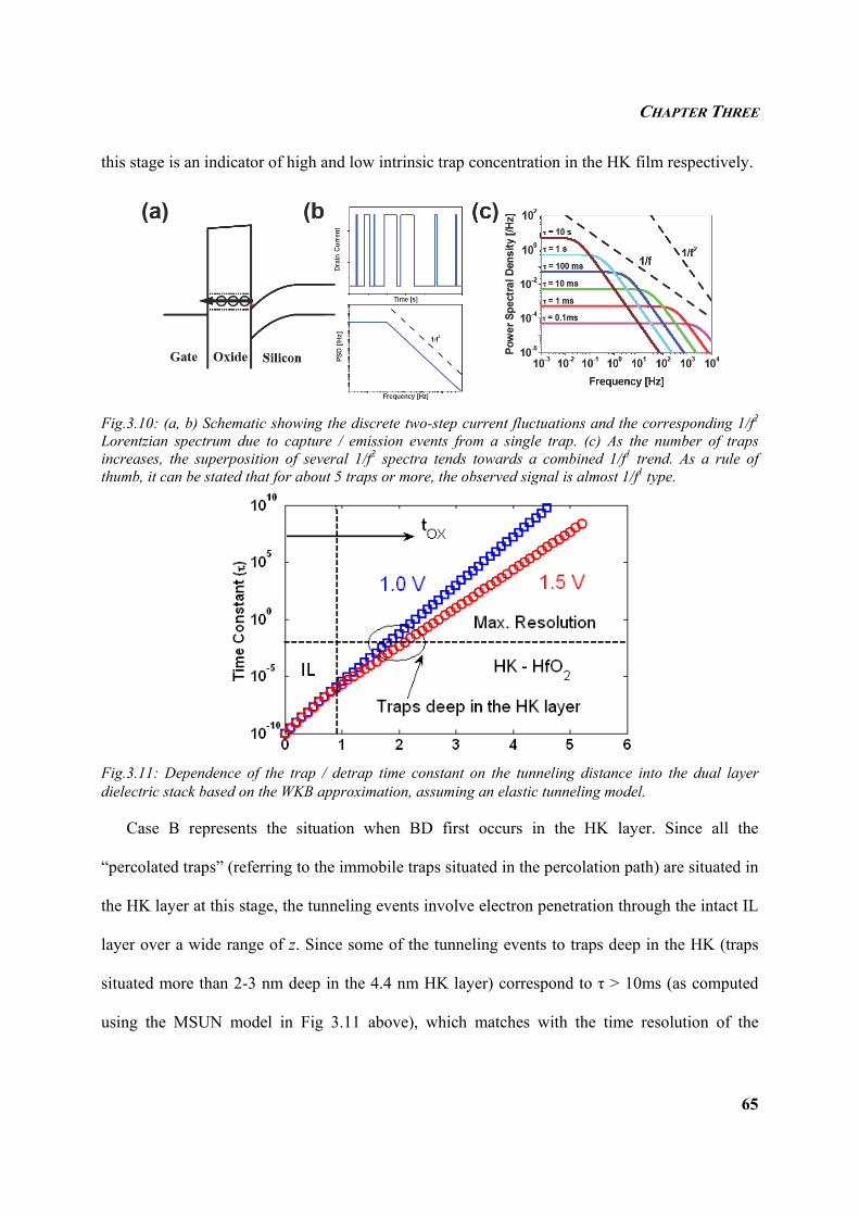
CHAPTER THREE
65
this stage is an indicator of high and low intrinsic trap concentration in the HK film respectively.
Fig.3.10: (a, b) Schematic showing the discrete two-step current fluctuations and the corresponding 1/f2 Lorentzian spectrum due to capture / emission events from a single trap. (c) As the number of traps increases, the superposition of several 1/f2 spectra tends towards a combined 1/f1 trend. As a rule of thumb, it can be stated that for about 5 traps or more, the observed signal is almost 1/f1 type.
Fig.3.11: Dependence of the trap / detrap time constant on the tunneling distance into the dual layer dielectric stack based on the WKB approximation, assuming an elastic tunneling model.
Case B represents the situation when BD first occurs in the HK layer. Since all the
“percolated traps” (referring to the immobile traps situated in the percolation path) are situated in
the HK layer at this stage, the tunneling events involve electron penetration through the intact IL
layer over a wide range of z. Since some of the tunneling events to traps deep in the HK (traps
situated more than 2-3 nm deep in the 4.4 nm HK layer) correspond to τ > 10ms (as computed
using the MSUN model in Fig 3.11 above), which matches with the time resolution of the
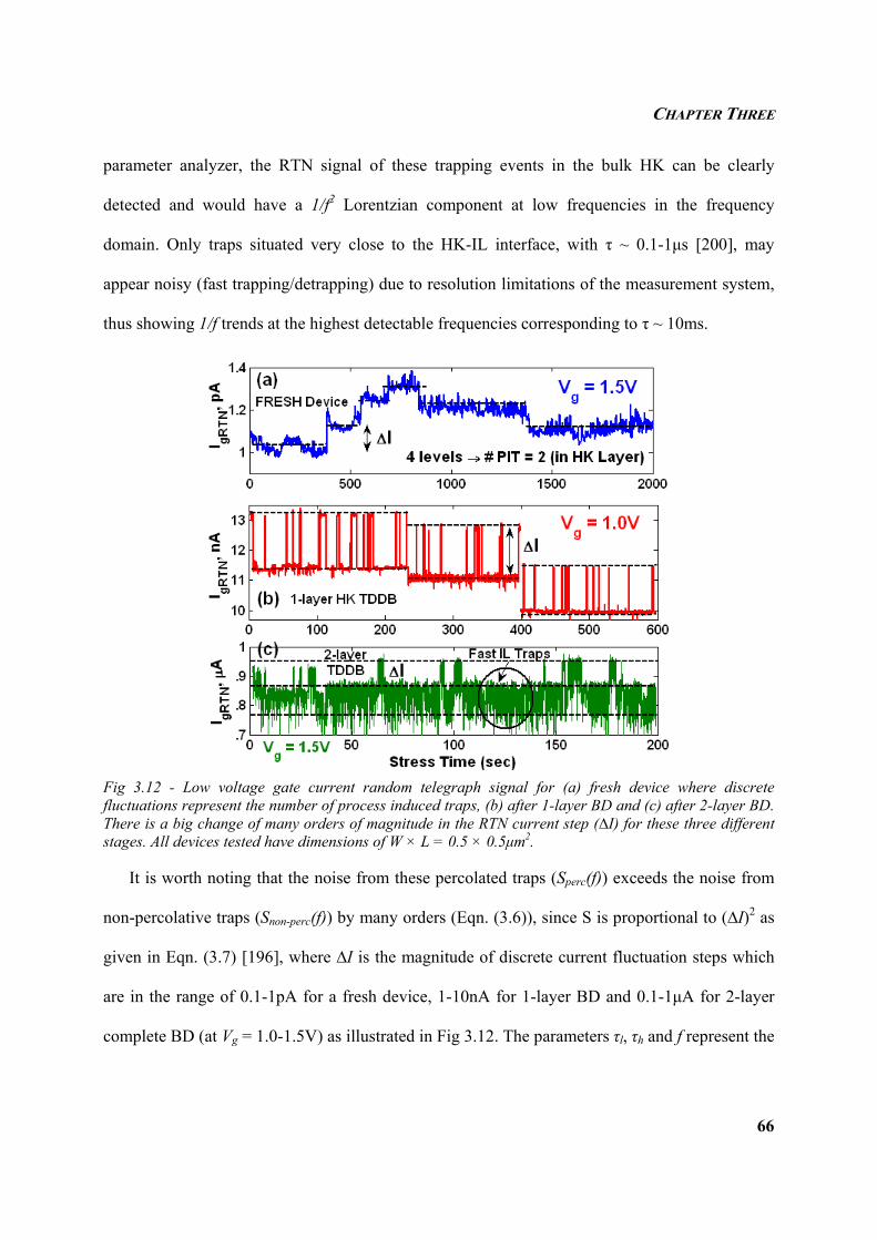
CHAPTER THREE
66
parameter analyzer, the RTN signal of these trapping events in the bulk HK can be clearly
detected and would have a 1/f2 Lorentzian component at low frequencies in the frequency
domain. Only traps situated very close to the HK-IL interface, with τ ~ 0.1-1µs [200], may
appear noisy (fast trapping/detrapping) due to resolution limitations of the measurement system,
thus showing 1/f trends at the highest detectable frequencies corresponding to τ ~ 10ms.
Fig 3.12 - Low voltage gate current random telegraph signal for (a) fresh device where discrete fluctuations represent the number of process induced traps, (b) after 1-layer BD and (c) after 2-layer BD. There is a big change of many orders of magnitude in the RTN current step (∆I) for these three different stages. All devices tested have dimensions of W × L = 0.5 × 0.5µm2.
It is worth noting that the noise from these percolated traps (Sperc(f)) exceeds the noise from
non-percolative traps (Snon-perc(f)) by many orders (Eqn. (3.6)), since S is proportional to (∆I)2 as
given in Eqn. (3.7) [196], where ∆I is the magnitude of discrete current fluctuation steps which
are in the range of 0.1-1pA for a fresh device, 1-10nA for 1-layer BD and 0.1-1µA for 2-layer
complete BD (at Vg = 1.0-1.5V) as illustrated in Fig 3.12. The parameters τl, τh and f represent the
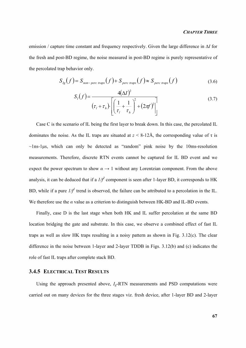
CHAPTER THREE
67
emission / capture time constant and frequency respectively. Given the large difference in ∆I for
the fresh and post-BD regime, the noise measured in post-BD regime is purely representative of
the percolated trap behavior only.
( ) ( ) ( ) ( )fSfSfSfS trapsperctrapsperctrapspercnonIg ≈+= − (3.6)
( ) ( )
( ) ( )⎥⎥⎦
⎤
⎢⎢⎣
⎡+⎟⎟
⎠
⎞⎜⎜⎝
⎛+⋅+
∆=
22
2
211
4
f
IfS
hlhl
I
πττ
ττ (3.7)
Case C is the scenario of IL being the first layer to break down. In this case, the percolated IL
dominates the noise. As the IL traps are situated at z < 8-12Å, the corresponding value of τ is
~1ns-1µs, which can only be detected as “random” pink noise by the 10ms-resolution
measurements. Therefore, discrete RTN events cannot be captured for IL BD event and we
expect the power spectrum to show α → 1 without any Lorentzian component. From the above
analysis, it can be deduced that if a 1/f2 component is seen after 1-layer BD, it corresponds to HK
BD, while if a pure 1/f1 trend is observed, the failure can be attributed to a percolation in the IL.
We therefore use the α value as a criterion to distinguish between HK-BD and IL-BD events.
Finally, case D is the last stage when both HK and IL suffer percolation at the same BD
location bridging the gate and substrate. In this case, we observe a combined effect of fast IL
traps as well as slow HK traps resulting in a noisy pattern as shown in Fig. 3.12(c). The clear
difference in the noise between 1-layer and 2-layer TDDB in Figs. 3.12(b) and (c) indicates the
role of fast IL traps after complete stack BD.
3.4.5 ELECTRICAL TEST RESULTS
Using the approach presented above, Ig-RTN measurements and PSD computations were
carried out on many devices for the three stages viz. fresh device, after 1-layer BD and 2-layer
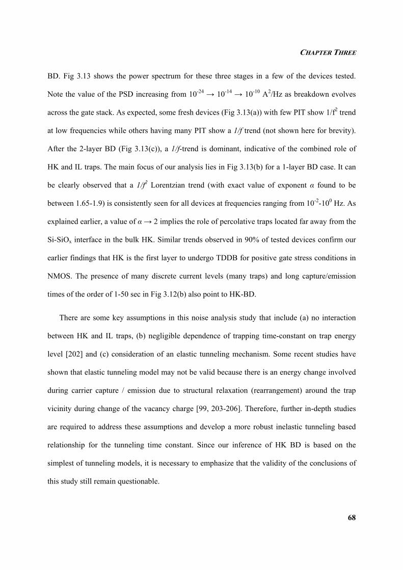
CHAPTER THREE
68
BD. Fig 3.13 shows the power spectrum for these three stages in a few of the devices tested.
Note the value of the PSD increasing from 10-24 → 10-14 → 10-10 A2/Hz as breakdown evolves
across the gate stack. As expected, some fresh devices (Fig 3.13(a)) with few PIT show 1/f2 trend
at low frequencies while others having many PIT show a 1/f trend (not shown here for brevity).
After the 2-layer BD (Fig 3.13(c)), a 1/f-trend is dominant, indicative of the combined role of
HK and IL traps. The main focus of our analysis lies in Fig 3.13(b) for a 1-layer BD case. It can
be clearly observed that a 1/f2 Lorentzian trend (with exact value of exponent α found to be
between 1.65-1.9) is consistently seen for all devices at frequencies ranging from 10-2-100 Hz. As
explained earlier, a value of α → 2 implies the role of percolative traps located far away from the
Si-SiOx interface in the bulk HK. Similar trends observed in 90% of tested devices confirm our
earlier findings that HK is the first layer to undergo TDDB for positive gate stress conditions in
NMOS. The presence of many discrete current levels (many traps) and long capture/emission
times of the order of 1-50 sec in Fig 3.12(b) also point to HK-BD.
There are some key assumptions in this noise analysis study that include (a) no interaction
between HK and IL traps, (b) negligible dependence of trapping time-constant on trap energy
level [202] and (c) consideration of an elastic tunneling mechanism. Some recent studies have
shown that elastic tunneling model may not be valid because there is an energy change involved
during carrier capture / emission due to structural relaxation (rearrangement) around the trap
vicinity during change of the vacancy charge [99, 203-206]. Therefore, further in-depth studies
are required to address these assumptions and develop a more robust inelastic tunneling based
relationship for the tunneling time constant. Since our inference of HK BD is based on the
simplest of tunneling models, it is necessary to emphasize that the validity of the conclusions of
this study still remain questionable.
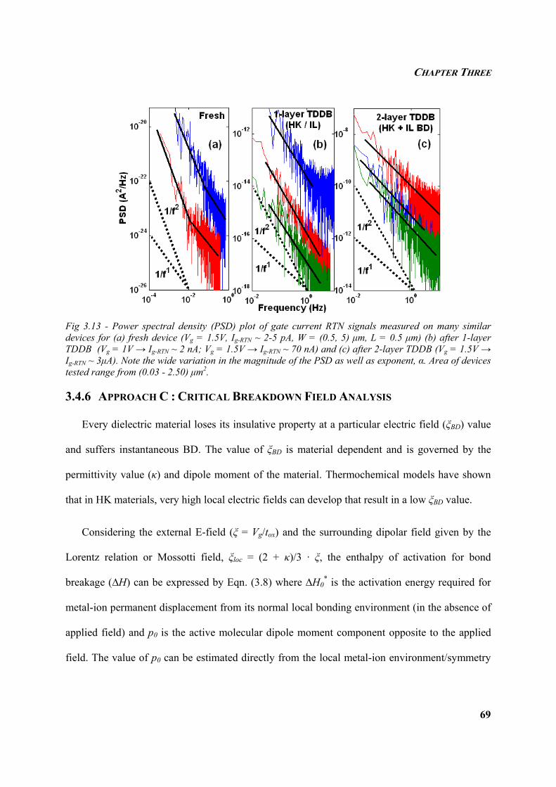
CHAPTER THREE
69
Fig 3.13 - Power spectral density (PSD) plot of gate current RTN signals measured on many similar devices for (a) fresh device (Vg = 1.5V, Ig-RTN ~ 2-5 pA, W = (0.5, 5) µm, L = 0.5 µm) (b) after 1-layer TDDB (Vg = 1V → Ig-RTN ~ 2 nA; Vg = 1.5V → Ig-RTN ~ 70 nA) and (c) after 2-layer TDDB (Vg = 1.5V → Ig-RTN ~ 3µA). Note the wide variation in the magnitude of the PSD as well as exponent, α. Area of devices tested range from (0.03 - 2.50) µm2.
3.4.6 APPROACH C : CRITICAL BREAKDOWN FIELD ANALYSIS
Every dielectric material loses its insulative property at a particular electric field (ξBD) value
and suffers instantaneous BD. The value of ξBD is material dependent and is governed by the
permittivity value (κ) and dipole moment of the material. Thermochemical models have shown
that in HK materials, very high local electric fields can develop that result in a low ξBD value.
Considering the external E-field (ξ = Vg/tox) and the surrounding dipolar field given by the
Lorentz relation or Mossotti field, ξloc = (2 + κ)/3 · ξ, the enthalpy of activation for bond
breakage (∆H) can be expressed by Eqn. (3.8) where ∆H0* is the activation energy required for
metal-ion permanent displacement from its normal local bonding environment (in the absence of
applied field) and p0 is the active molecular dipole moment component opposite to the applied
field. The value of p0 can be estimated directly from the local metal-ion environment/symmetry
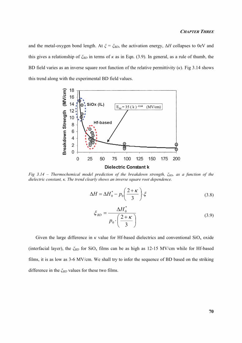
CHAPTER THREE
70
and the metal-oxygen bond length. At ξ = ξBD, the activation energy, ∆H collapses to 0eV and
this gives a relationship of ξBD in terms of κ as in Eqn. (3.9). In general, as a rule of thumb, the
BD field varies as an inverse square root function of the relative permittivity (κ). Fig 3.14 shows
this trend along with the experimental BD field values.
Fig 3.14 – Thermochemical model prediction of the breakdown strength, ξBD, as a function of the dielectric constant, κ. The trend clearly shows an inverse square root dependence.
ξκ⋅⎟⎠⎞
⎜⎝⎛ +
−∆=∆3
20
*0 pHH (3.8)
⎟⎠⎞
⎜⎝⎛ +⋅
∆=
32
0
*0
κξ
p
HBD (3.9)
Given the large difference in κ value for Hf-based dielectrics and conventional SiOx oxide
(interfacial layer), the ξBD for SiOx films can be as high as 12-15 MV/cm while for Hf-based
films, it is as low as 3-6 MV/cm. We shall try to infer the sequence of BD based on the striking
difference in the ξBD values for these two films.
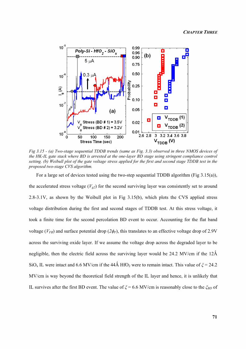
CHAPTER THREE
71
Fig 3.15 - (a) Two-stage sequential TDDB trends (same as Fig. 3.3) observed in three NMOS devices of the HK-IL gate stack where BD is arrested at the one-layer BD stage using stringent compliance control setting. (b) Weibull plot of the gate voltage stress applied for the first and second stage TDDB test in the proposed two-stage CVS algorithm.
For a large set of devices tested using the two-step sequential TDDB algorithm (Fig 3.15(a)),
the accelerated stress voltage (Vg2) for the second surviving layer was consistently set to around
2.8-3.1V, as shown by the Weibull plot in Fig 3.15(b), which plots the CVS applied stress
voltage distribution during the first and second stages of TDDB test. At this stress voltage, it
took a finite time for the second percolation BD event to occur. Accounting for the flat band
voltage (VFB) and surface potential drop (2φF), this translates to an effective voltage drop of 2.9V
across the surviving oxide layer. If we assume the voltage drop across the degraded layer to be
negligible, then the electric field across the surviving layer would be 24.2 MV/cm if the 12Ǻ
SiOx IL were intact and 6.6 MV/cm if the 44Ǻ HfO2 were to remain intact. This value of ξ = 24.2
MV/cm is way beyond the theoretical field strength of the IL layer and hence, it is unlikely that
IL survives after the first BD event. The value of ξ = 6.6 MV/cm is reasonably close to the ξBD of
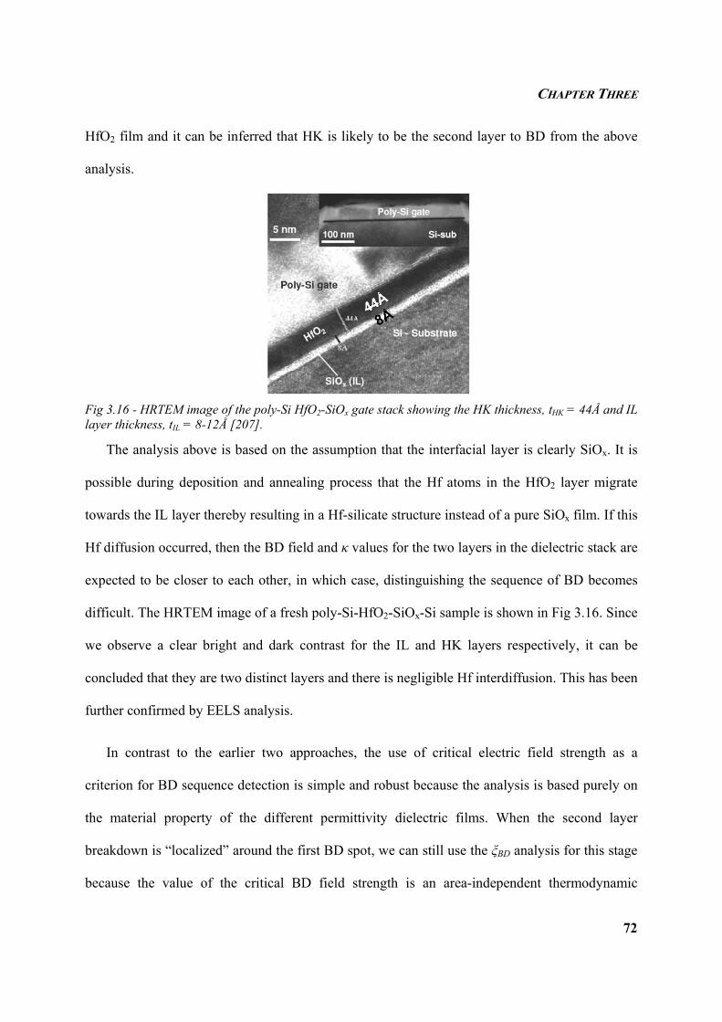
CHAPTER THREE
72
HfO2 film and it can be inferred that HK is likely to be the second layer to BD from the above
analysis.
Fig 3.16 - HRTEM image of the poly-Si HfO2-SiOx gate stack showing the HK thickness, tHK = 44Å and IL layer thickness, tIL = 8-12Å [207].
The analysis above is based on the assumption that the interfacial layer is clearly SiOx. It is
possible during deposition and annealing process that the Hf atoms in the HfO2 layer migrate
towards the IL layer thereby resulting in a Hf-silicate structure instead of a pure SiOx film. If this
Hf diffusion occurred, then the BD field and κ values for the two layers in the dielectric stack are
expected to be closer to each other, in which case, distinguishing the sequence of BD becomes
difficult. The HRTEM image of a fresh poly-Si-HfO2-SiOx-Si sample is shown in Fig 3.16. Since
we observe a clear bright and dark contrast for the IL and HK layers respectively, it can be
concluded that they are two distinct layers and there is negligible Hf interdiffusion. This has been
further confirmed by EELS analysis.
In contrast to the earlier two approaches, the use of critical electric field strength as a
criterion for BD sequence detection is simple and robust because the analysis is based purely on
the material property of the different permittivity dielectric films. When the second layer
breakdown is “localized” around the first BD spot, we can still use the ξBD analysis for this stage
because the value of the critical BD field strength is an area-independent thermodynamic
CHAPTER THREE
73
quantity representing the activation barrier for bond breakage of the Hf-O and/or Si-O bonds. For
a more accurate analysis, we can reuse Gauss law to account for the marginal non-zero voltage
drop (which we previously ignored) across the broken down layer during the second stage of
stress, as the first-layer BD (which corresponds to a SBD event with an oxygen-deficient
percolated region) may not have metallic-like low resistivity for voltage drop across it to be fully
ignored. However, we have verified that the result of the BD sequence does not change even if
the more accurate analysis based on Gauss law calculations is carried out.
Analyzing this scenario from a process point of view, it is but natural to expect the IL layer
to break down first because the HfO2 has a tendency to scavenge oxygen atoms from the ultra-
thin IL layer [208] that cause the SiOx to become all the more oxygen deficient (many process
induced traps prior to stress). Moreover, the ultra-thin SiOx is generally under high compressive
strain [209], which causes it to undergo structural relaxation by means of bond breaking, so that
the system free energy can be minimized. The stress in these nanoscale ultra-thin films also
serves as a precursor for soft breakdown of the dielectric.
3.4.7 SUMMARY OF BREAKDOWN SEQUENCE
Three different approaches have been presented in this chapter, aimed at deciphering the
sequence of BD in a dual layer HK-IL gate dielectric stack. The first two approaches using
Poole-Frenkel emission studies and 1/f noise analysis results indicate HK to be the first layer to
BD, while the simplistic electric field analysis suggests IL to be the first one. The ξ-field analysis
approach seems to suggest that the sequence of BD should be independent of the voltage polarity
(substrate / gate injection) and only depend on the effective voltage drop across the HK and IL
layers as given by Gauss Law. However, some literature results clearly point to a polarity
dependent BD trend [210]. While each method of detection has its own shortcomings and
CHAPTER THREE
74
inherent assumptions, the critical BD electric field strength based study is the most convincing
and robust method as we do not make any simplifying assumptions in this case and therefore, we
can conclude here that IL is likely to be the first layer to BD for the 44Ǻ-HK, 8-12 Ǻ-IL stack.
Though we only considered one particular combination of tHK : tIL for the analysis, in general, it
can be inferred that the IL is more susceptible to percolation for any combination of HK/IL
dielectric thickness values. We will further confirm this using thermochemical Monte Carlo
statistical simulations in the next chapter.
3.5 POST BREAKDOWN RELIABILITY OF DUAL LAYER STACKS
3.5.1 CURRENT KNOWHOW ON POST BREAKDOWN RELIABILITY
Reliability at the post-BD stage has always been an important area of study as it is very
critical to find out whether the MOSFET device performance characteristics are still
“acceptable” after a soft BD of the dielectric. The duration after the TDDB event for which the
degraded transistor is still able to function effectively can be considered as an additional
reliability margin at both the device and circuit levels. The physics and statistics [36, 211, 212]
of post-BD have been extensively studied for the single-layer SiON / SiO2 in the past. It is well
documented that the post-BD stage can be divided into two regimes [213-216] – an initial regime
of digital gate current (referred to as Di-BD) fluctuations due to the stochastic carrier capture and
emission events at the percolated traps and a subsequent wear-out analog breakdown (An-BD)
regime which involves dilation of the percolation path and/or nucleation of microstructural
defects such as the DBIE that causes effective oxide thinning [101]. As mentioned earlier in
Chapter 2, the transition from the digital to analog wear-out regime in SiON is governed by a
critical voltage (Vcrit) [117].
For the case of post-BD in MG-HK stacks, there have been some recent initial electrical
CHAPTER THREE
75
studies as well [217, 218]; however in-depth analysis for these dual layer stacks is still required.
It is necessary to know how robust the HK-IL stack is to resist analog wear-out both for the cases
of a single layer IL BD and for the case of the complete HK+IL stack BD. This is the focus of
our study in this section. We will assess the post-BD reliability by borrowing the concept of Vcrit
in SiON and apply it to the HK-IL stack.
3.5.2 APPLICATION OF CRITICAL VOLTAGE FOR MG-HK STACK ANALOG BD
The critical voltage (Vcrit) concept was initially proposed by Lo et. al. [117] for SiON
dielectric to refer to the minimum voltage below which the digital fluctuation regime of BD does
not evolve into the analog wear-out regime at all, due to insufficient driving force (Joule heating,
temperature and trap generation). Fig 3.17(a) shows the post-BD Ig-t evolution trend in a 16Ǻ
SiON gate stack at a reasonably high voltage of Vg = 2.6V. Note that a clear transition and
evolution from the initial Di-BD to An-BD is observed in “finite” time. The RTN signals at
lower voltages are clearly evident in Fig 3.17(b).
The trend of linear variation in Vcrit for various oxide thicknesses, tox, ranging from 12-22Ǻ,
is plotted in Fig. 3.18 [101]. Note the general trend of decrease in Vcrit for lower tox values. This
trend is expected because the leakage current density induced temperature and subsequent
temperature induced trap generation effects are more severe for any given post-BD voltage as tox
is reduced, considering the fact that a lower number of probabilistic trap assisted tunneling
(hopping) events (implying increased leakage) is needed for a shorter percolation path. It can be
observed that for a typical tox = 16Ǻ, Vcrit ranges between 2.0-2.5V which is much larger than the
operating voltage of Vop = 1V. This leads us to infer that the digital regime is very prolonged in
the case of a 16Ǻ SiON, thereby providing very good reliability margin, since device
performance is reasonably good for this stage, as verified in Ref. [101]. It is also worth noting
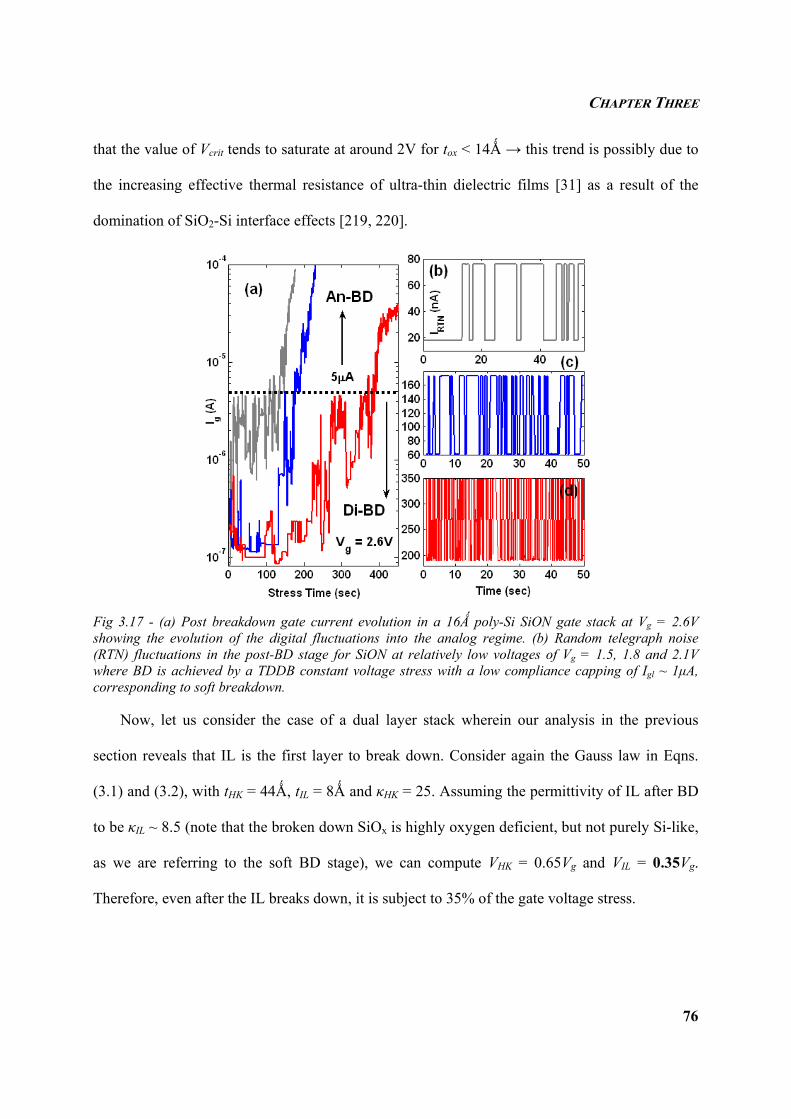
CHAPTER THREE
76
that the value of Vcrit tends to saturate at around 2V for tox < 14Ǻ → this trend is possibly due to
the increasing effective thermal resistance of ultra-thin dielectric films [31] as a result of the
domination of SiO2-Si interface effects [219, 220].
Fig 3.17 - (a) Post breakdown gate current evolution in a 16Ǻ poly-Si SiON gate stack at Vg = 2.6V showing the evolution of the digital fluctuations into the analog regime. (b) Random telegraph noise (RTN) fluctuations in the post-BD stage for SiON at relatively low voltages of Vg = 1.5, 1.8 and 2.1V where BD is achieved by a TDDB constant voltage stress with a low compliance capping of Igl ~ 1µA, corresponding to soft breakdown.
Now, let us consider the case of a dual layer stack wherein our analysis in the previous
section reveals that IL is the first layer to break down. Consider again the Gauss law in Eqns.
(3.1) and (3.2), with tHK = 44Ǻ, tIL = 8Ǻ and κHK = 25. Assuming the permittivity of IL after BD
to be κIL ~ 8.5 (note that the broken down SiOx is highly oxygen deficient, but not purely Si-like,
as we are referring to the soft BD stage), we can compute VHK = 0.65Vg and VIL = 0.35Vg.
Therefore, even after the IL breaks down, it is subject to 35% of the gate voltage stress.
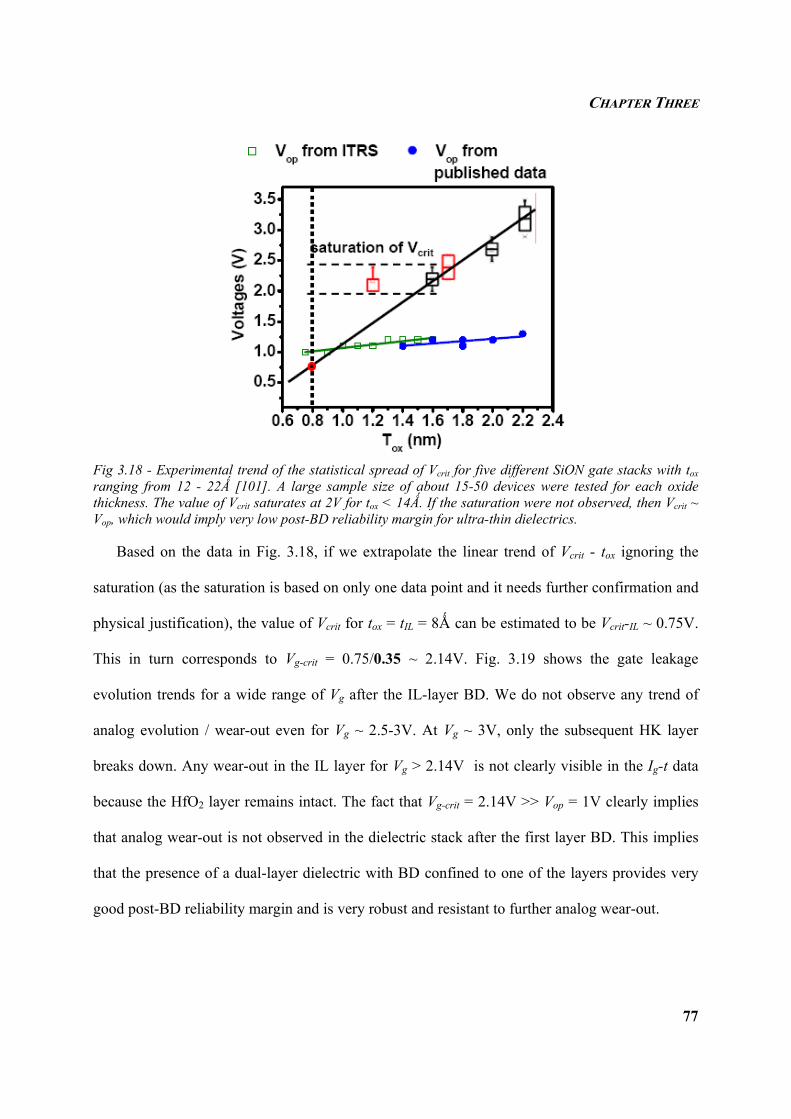
CHAPTER THREE
77
Fig 3.18 - Experimental trend of the statistical spread of Vcrit for five different SiON gate stacks with tox ranging from 12 - 22Ǻ [101]. A large sample size of about 15-50 devices were tested for each oxide thickness. The value of Vcrit saturates at 2V for tox < 14Ǻ. If the saturation were not observed, then Vcrit ~ Vop, which would imply very low post-BD reliability margin for ultra-thin dielectrics.
Based on the data in Fig. 3.18, if we extrapolate the linear trend of Vcrit - tox ignoring the
saturation (as the saturation is based on only one data point and it needs further confirmation and
physical justification), the value of Vcrit for tox = tIL = 8Ǻ can be estimated to be Vcrit-IL ~ 0.75V.
This in turn corresponds to Vg-crit = 0.75/0.35 ~ 2.14V. Fig. 3.19 shows the gate leakage
evolution trends for a wide range of Vg after the IL-layer BD. We do not observe any trend of
analog evolution / wear-out even for Vg ~ 2.5-3V. At Vg ~ 3V, only the subsequent HK layer
breaks down. Any wear-out in the IL layer for Vg > 2.14V is not clearly visible in the Ig-t data
because the HfO2 layer remains intact. The fact that Vg-crit = 2.14V >> Vop = 1V clearly implies
that analog wear-out is not observed in the dielectric stack after the first layer BD. This implies
that the presence of a dual-layer dielectric with BD confined to one of the layers provides very
good post-BD reliability margin and is very robust and resistant to further analog wear-out.
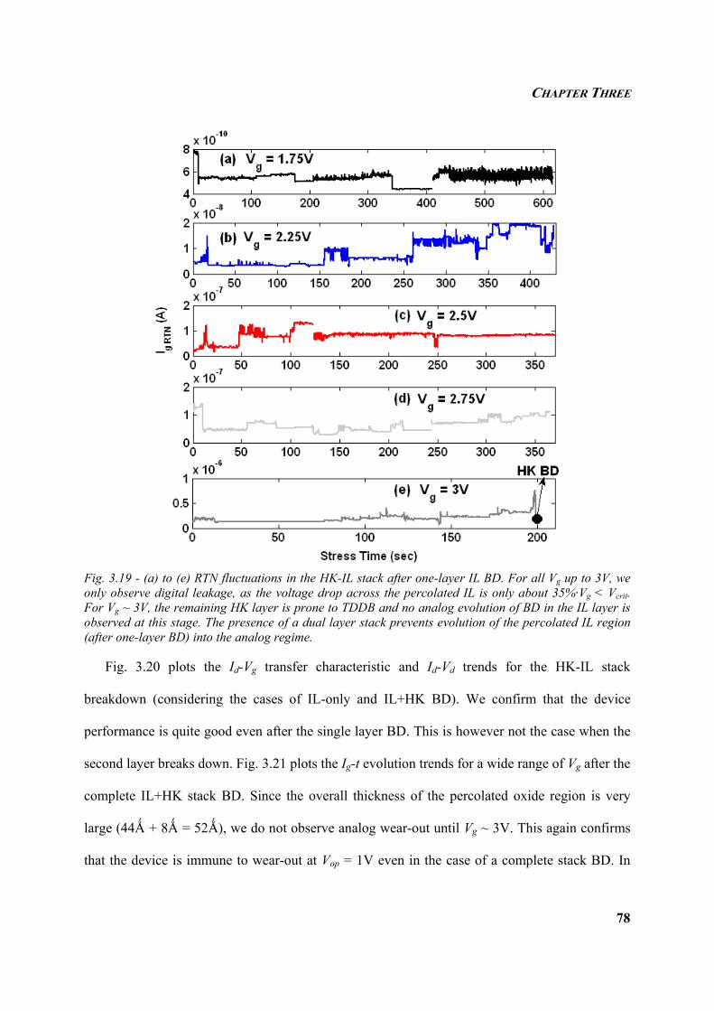
CHAPTER THREE
78
Fig. 3.19 - (a) to (e) RTN fluctuations in the HK-IL stack after one-layer IL BD. For all Vg up to 3V, we only observe digital leakage, as the voltage drop across the percolated IL is only about 35%·Vg < Vcrit. For Vg ~ 3V, the remaining HK layer is prone to TDDB and no analog evolution of BD in the IL layer is observed at this stage. The presence of a dual layer stack prevents evolution of the percolated IL region (after one-layer BD) into the analog regime.
Fig. 3.20 plots the Id-Vg transfer characteristic and Id-Vd trends for the HK-IL stack
breakdown (considering the cases of IL-only and IL+HK BD). We confirm that the device
performance is quite good even after the single layer BD. This is however not the case when the
second layer breaks down. Fig. 3.21 plots the Ig-t evolution trends for a wide range of Vg after the
complete IL+HK stack BD. Since the overall thickness of the percolated oxide region is very
large (44Ǻ + 8Ǻ = 52Ǻ), we do not observe analog wear-out until Vg ~ 3V. This again confirms
that the device is immune to wear-out at Vop = 1V even in the case of a complete stack BD. In
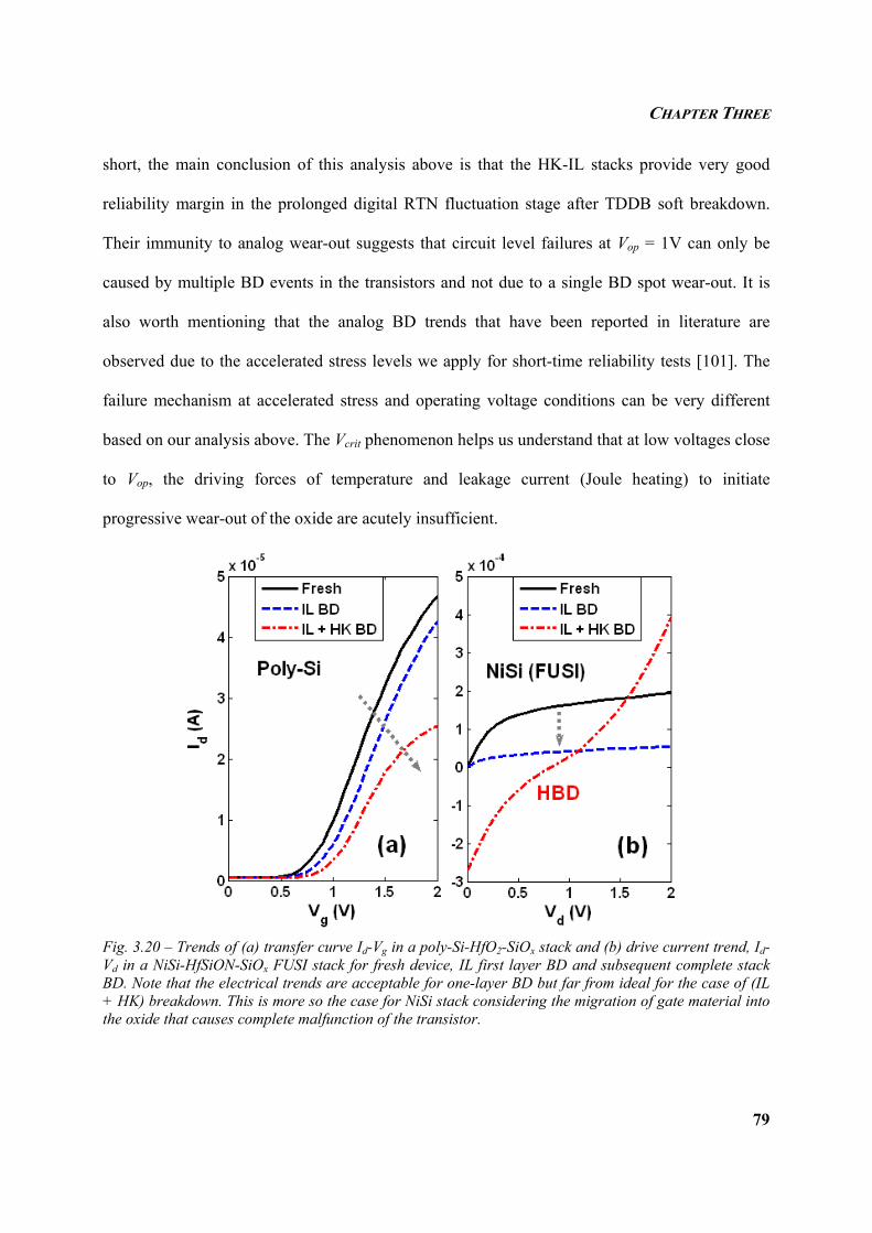
CHAPTER THREE
79
short, the main conclusion of this analysis above is that the HK-IL stacks provide very good
reliability margin in the prolonged digital RTN fluctuation stage after TDDB soft breakdown.
Their immunity to analog wear-out suggests that circuit level failures at Vop = 1V can only be
caused by multiple BD events in the transistors and not due to a single BD spot wear-out. It is
also worth mentioning that the analog BD trends that have been reported in literature are
observed due to the accelerated stress levels we apply for short-time reliability tests [101]. The
failure mechanism at accelerated stress and operating voltage conditions can be very different
based on our analysis above. The Vcrit phenomenon helps us understand that at low voltages close
to Vop, the driving forces of temperature and leakage current (Joule heating) to initiate
progressive wear-out of the oxide are acutely insufficient.
Fig. 3.20 – Trends of (a) transfer curve Id-Vg in a poly-Si-HfO2-SiOx stack and (b) drive current trend, Id-Vd in a NiSi-HfSiON-SiOx FUSI stack for fresh device, IL first layer BD and subsequent complete stack BD. Note that the electrical trends are acceptable for one-layer BD but far from ideal for the case of (IL + HK) breakdown. This is more so the case for NiSi stack considering the migration of gate material into the oxide that causes complete malfunction of the transistor.
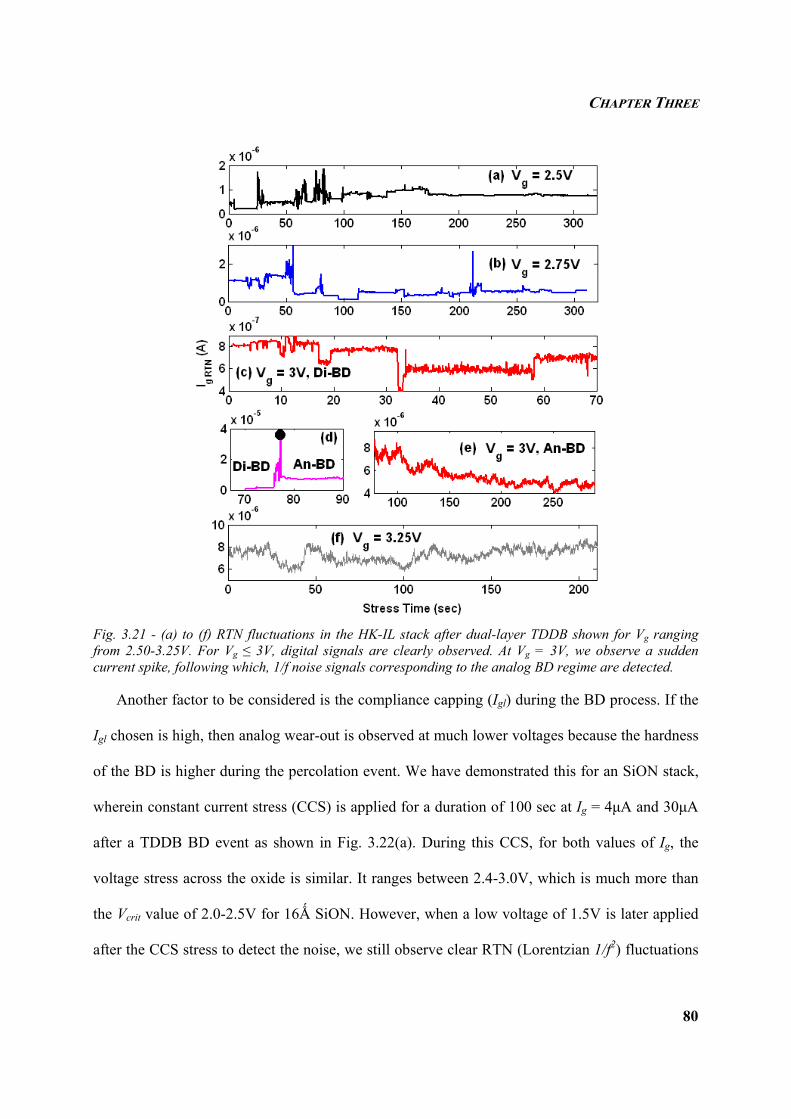
CHAPTER THREE
80
Fig. 3.21 - (a) to (f) RTN fluctuations in the HK-IL stack after dual-layer TDDB shown for Vg ranging from 2.50-3.25V. For Vg ≤ 3V, digital signals are clearly observed. At Vg = 3V, we observe a sudden current spike, following which, 1/f noise signals corresponding to the analog BD regime are detected.
Another factor to be considered is the compliance capping (Igl) during the BD process. If the
Igl chosen is high, then analog wear-out is observed at much lower voltages because the hardness
of the BD is higher during the percolation event. We have demonstrated this for an SiON stack,
wherein constant current stress (CCS) is applied for a duration of 100 sec at Ig = 4µA and 30µA
after a TDDB BD event as shown in Fig. 3.22(a). During this CCS, for both values of Ig, the
voltage stress across the oxide is similar. It ranges between 2.4-3.0V, which is much more than
the Vcrit value of 2.0-2.5V for 16Ǻ SiON. However, when a low voltage of 1.5V is later applied
after the CCS stress to detect the noise, we still observe clear RTN (Lorentzian 1/f2) fluctuations
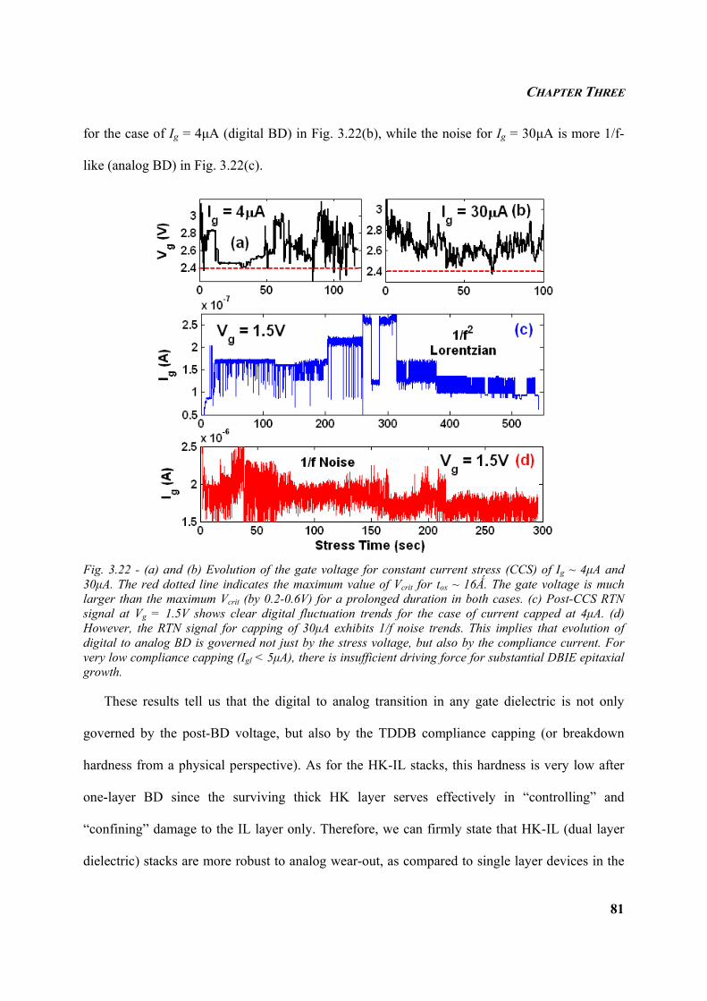
CHAPTER THREE
81
for the case of Ig = 4µA (digital BD) in Fig. 3.22(b), while the noise for Ig = 30µA is more 1/f-
like (analog BD) in Fig. 3.22(c).
Fig. 3.22 - (a) and (b) Evolution of the gate voltage for constant current stress (CCS) of Ig ~ 4µA and 30µA. The red dotted line indicates the maximum value of Vcrit for tox ~ 16Ǻ. The gate voltage is much larger than the maximum Vcrit (by 0.2-0.6V) for a prolonged duration in both cases. (c) Post-CCS RTN signal at Vg = 1.5V shows clear digital fluctuation trends for the case of current capped at 4µA. (d) However, the RTN signal for capping of 30µA exhibits 1/f noise trends. This implies that evolution of digital to analog BD is governed not just by the stress voltage, but also by the compliance current. For very low compliance capping (Igl < 5µA), there is insufficient driving force for substantial DBIE epitaxial growth.
These results tell us that the digital to analog transition in any gate dielectric is not only
governed by the post-BD voltage, but also by the TDDB compliance capping (or breakdown
hardness from a physical perspective). As for the HK-IL stacks, this hardness is very low after
one-layer BD since the surviving thick HK layer serves effectively in “controlling” and
“confining” damage to the IL layer only. Therefore, we can firmly state that HK-IL (dual layer
dielectric) stacks are more robust to analog wear-out, as compared to single layer devices in the
CHAPTER THREE
82
older technology nodes, such as SiO2 and SiON. However, considering recent developments
towards realizing zero-IL (ZIL) devices [66] with a single ultra-thin HK dielectric layer aimed at
extreme EOT scaling, the problem of analog wear-out may pose to be a serious reliability
concern yet again for future sub-16 nm technology nodes.
3.6 SUMMARY
In this chapter, we addressed an important topic regarding the sequence of breakdown in HK-
IL stacks using three different electrical characterization techniques. Based on our analysis of the
assumptions in the application of these techniques, we concluded that the critical electric field
strength analysis is the most robust as it takes advantage of the intrinsic distinctive material
properties of the HfO2 and SiOx films. We deduced that the IL layer is the first to BD for any
given dual layer dielectric stack. This was followed by an analysis of the post-BD reliability
which revealed that HK-IL devices are very resilient to percolative wear-out because the intact
HK (after IL BD) ensures low leakage, which in turn translates to insignificant Joule heating and
electro-thermal stresses that are needed for analog leakage degradation. The results confirm that
the HK-IL combination is a robust stack and in all likelihood, circuit level failure may be caused
only by multiple IL SBD events, rather than a complete HK-IL stack BD. Having deciphered the
BD sequence, we will use this information in the next chapter to develop a statistical model for
lifetime estimation of the HK-IL TDDB phenomenon.
CHAPTER FOUR
83
CHAPTER FOUR
SSSTTTAAATTTIIISSSTTTIIICCCAAALLL MMMOOODDDEEELLLIIINNNGGG AAANNNDDD AAANNNAAALLLYYYSSSIIISSS OOOFFF
DDDUUUAAALLL LLLAAAYYYEEERRR DDDIIIEEELLLEEECCCTTTRRRIIICCC SSSTTTAAACCCKKKSSS
4.1 INTRODUCTION
The ultimate aim of any reliability study is to quantify the lifetime expected at nominal
operating conditions based on the accelerated stress tests that the device is subjected to in order
to measure the time to failure. This involves the use of suitable physical / empirical models to
extrapolate the failure time. The technology is qualified for commercial use if the estimated
lifetime at nominal conditions exceeds a certain pre-determined target, which is typically 10
years for any failure mechanism in advanced semiconductor technology nodes. The methodology
used for statistical lifetime assessment is a very critical component of reliability analysis. If the
wrong statistical distributions are used or if the wrong extrapolation model is used, then the
resulting estimates of the device / product lifetime tend to be erroneous (by many orders of
magnitude) and all the efforts and resources spent on reliability tests are wasted. It is therefore
very important to find the most suited statistical models that can describe the physics of failure of
a particular failure mechanism very accurately. In this chapter, we will begin with the
conventional established reliability modeling approach for TDDB in single layer dielectrics such
as SiO2 and SiON and subsequently investigate the reasons for the invalidity of these statistical
approaches for direct application to HK-IL reliability assessment. In view of the limitations of
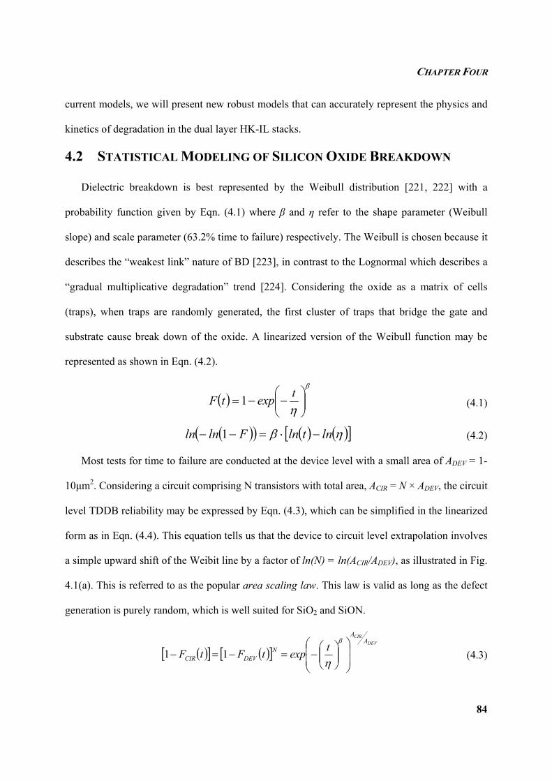
CHAPTER FOUR
84
current models, we will present new robust models that can accurately represent the physics and
kinetics of degradation in the dual layer HK-IL stacks.
4.2 STATISTICAL MODELING OF SILICON OXIDE BREAKDOWN
Dielectric breakdown is best represented by the Weibull distribution [221, 222] with a
probability function given by Eqn. (4.1) where β and η refer to the shape parameter (Weibull
slope) and scale parameter (63.2% time to failure) respectively. The Weibull is chosen because it
describes the “weakest link” nature of BD [223], in contrast to the Lognormal which describes a
“gradual multiplicative degradation” trend [224]. Considering the oxide as a matrix of cells
(traps), when traps are randomly generated, the first cluster of traps that bridge the gate and
substrate cause break down of the oxide. A linearized version of the Weibull function may be
represented as shown in Eqn. (4.2).
( )β
η ⎟⎟⎠
⎞⎜⎜⎝
⎛−−=
texptF 1 (4.1)
( )( ) ( ) ( )[ ]ηβ lntlnFlnln −⋅=−− 1 (4.2)
Most tests for time to failure are conducted at the device level with a small area of ADEV = 1-
10µm2. Considering a circuit comprising N transistors with total area, ACIR = N × ADEV, the circuit
level TDDB reliability may be expressed by Eqn. (4.3), which can be simplified in the linearized
form as in Eqn. (4.4). This equation tells us that the device to circuit level extrapolation involves
a simple upward shift of the Weibit line by a factor of ln(N) = ln(ACIR/ADEV), as illustrated in Fig.
4.1(a). This is referred to as the popular area scaling law. This law is valid as long as the defect
generation is purely random, which is well suited for SiO2 and SiON.
( )[ ] ( )[ ]DEV
CIRA
A
NDEVCIR
texptFtF⎟⎟
⎠
⎞
⎜⎜
⎝
⎛⎟⎟⎠
⎞⎜⎜⎝
⎛−=−=−
β
η11 (4.3)
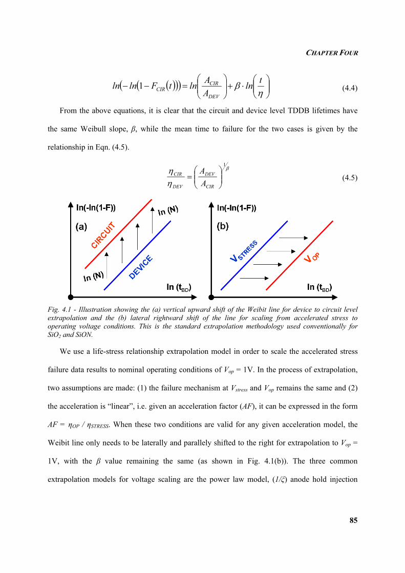
CHAPTER FOUR
85
( )( )( ) ⎟⎟⎠
⎞⎜⎜⎝
⎛⋅+⎟⎟
⎠
⎞⎜⎜⎝
⎛=−−
ηβ tln
AAlntFlnln
DEV
CIRCIR1 (4.4)
From the above equations, it is clear that the circuit and device level TDDB lifetimes have
the same Weibull slope, β, while the mean time to failure for the two cases is given by the
relationship in Eqn. (4.5).
β
ηη
1
⎟⎟⎠
⎞⎜⎜⎝
⎛=
CIR
DEV
DEV
CIR
AA
(4.5)
Fig. 4.1 - Illustration showing the (a) vertical upward shift of the Weibit line for device to circuit level extrapolation and the (b) lateral rightward shift of the line for scaling from accelerated stress to operating voltage conditions. This is the standard extrapolation methodology used conventionally for SiO2 and SiON.
We use a life-stress relationship extrapolation model in order to scale the accelerated stress
failure data results to nominal operating conditions of Vop = 1V. In the process of extrapolation,
two assumptions are made: (1) the failure mechanism at Vstress and Vop remains the same and (2)
the acceleration is “linear”, i.e. given an acceleration factor (AF), it can be expressed in the form
AF = ηOP / ηSTRESS. When these two conditions are valid for any given acceleration model, the
Weibit line only needs to be laterally and parallely shifted to the right for extrapolation to Vop =
1V, with the β value remaining the same (as shown in Fig. 4.1(b)). The three common
extrapolation models for voltage scaling are the power law model, (1/ξ) anode hold injection
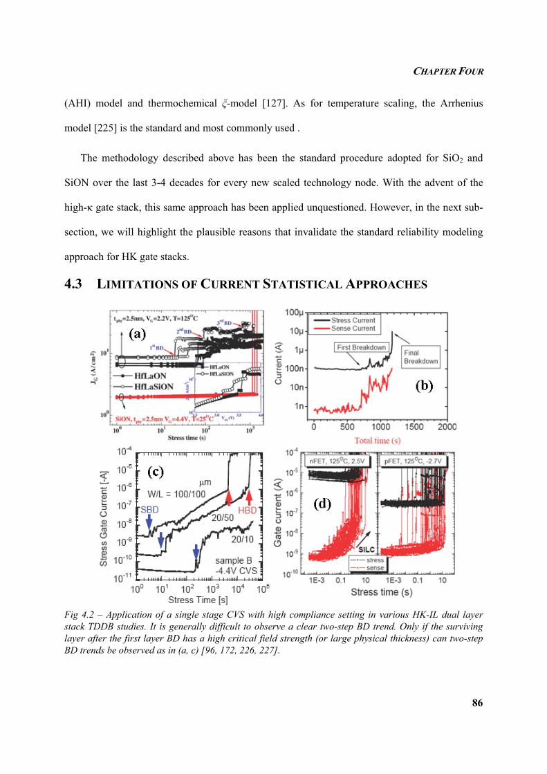
CHAPTER FOUR
86
(AHI) model and thermochemical ξ-model [127]. As for temperature scaling, the Arrhenius
model [225] is the standard and most commonly used .
The methodology described above has been the standard procedure adopted for SiO2 and
SiON over the last 3-4 decades for every new scaled technology node. With the advent of the
high-κ gate stack, this same approach has been applied unquestioned. However, in the next sub-
section, we will highlight the plausible reasons that invalidate the standard reliability modeling
approach for HK gate stacks.
4.3 LIMITATIONS OF CURRENT STATISTICAL APPROACHES
Fig 4.2 – Application of a single stage CVS with high compliance setting in various HK-IL dual layer stack TDDB studies. It is generally difficult to observe a clear two-step BD trend. Only if the surviving layer after the first layer BD has a high critical field strength (or large physical thickness) can two-step BD trends be observed as in (a, c) [96, 172, 226, 227].
CHAPTER FOUR
87
In the previous chapter, we discussed the need for developing a two-stage sequential BD
algorithm and highlighted the criticality of choosing the right compliance capping for the first
stage (Ig1) and stress voltage for the second stage (Vg2), so that the BD process can be arrested
and the two-step leakage jump trends clearly distinguished. Figs 4.2 and 4.3 [96, 172, 226-228]
show some results in the literature that use a single stage CVS and RVS respectively with a high
preset compliance value. It is obvious from these results that observation of two-stage BD is
unclear and rather absent and only for a few cases where the second surviving layer is very thick
(so that the condition ξ < ξBD holds true), can this trend be somewhat evident.
Fig 4.3 – Use of single stage ramp voltage stress (RVS) for HK-IL gate stacks. Again, there is no clear distinct observation of two-step BD here as the second surviving layer shows abrupt instantaneous percolation [172, 228].
For the above set of measured TBD / VBD data where it is hard to distinguish and decode the
two-stage BD trends, past studies have used the conventional Weibull plot analysis for TBD or
VBD, with arbitrary definitions for the instant of BD. The analysis also involves testing at
different stress voltages and using the inverse power law (IPL) relationship for extrapolation
[127] and the area scaling law to predict circuit level reliability lifetime [131]. The key
drawbacks of applying the above conventional approach used in oxynitride (SiON) analysis for
HK-IL stacks are as follows :-
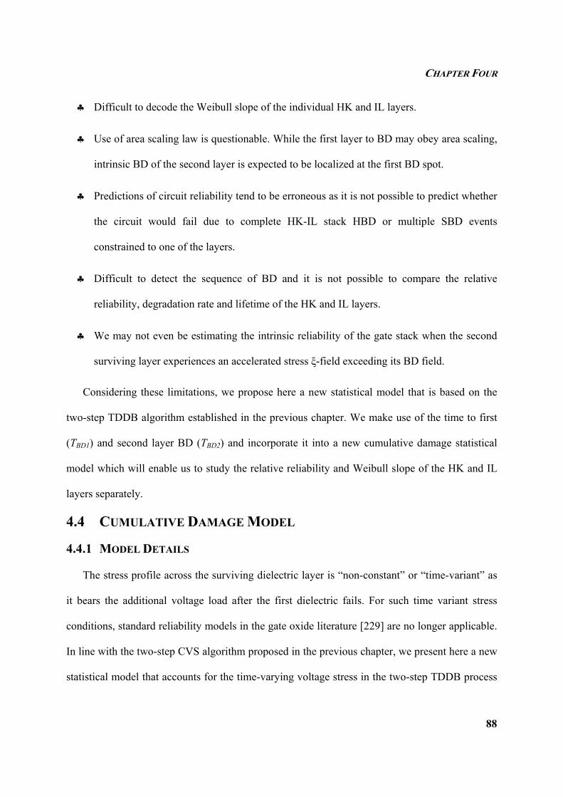
CHAPTER FOUR
88
♣ Difficult to decode the Weibull slope of the individual HK and IL layers.
♣ Use of area scaling law is questionable. While the first layer to BD may obey area scaling,
intrinsic BD of the second layer is expected to be localized at the first BD spot.
♣ Predictions of circuit reliability tend to be erroneous as it is not possible to predict whether
the circuit would fail due to complete HK-IL stack HBD or multiple SBD events
constrained to one of the layers.
♣ Difficult to detect the sequence of BD and it is not possible to compare the relative
reliability, degradation rate and lifetime of the HK and IL layers.
♣ We may not even be estimating the intrinsic reliability of the gate stack when the second
surviving layer experiences an accelerated stress ξ-field exceeding its BD field.
Considering these limitations, we propose here a new statistical model that is based on the
two-step TDDB algorithm established in the previous chapter. We make use of the time to first
(TBD1) and second layer BD (TBD2) and incorporate it into a new cumulative damage statistical
model which will enable us to study the relative reliability and Weibull slope of the HK and IL
layers separately.
4.4 CUMULATIVE DAMAGE MODEL
4.4.1 MODEL DETAILS
The stress profile across the surviving dielectric layer is “non-constant” or “time-variant” as
it bears the additional voltage load after the first dielectric fails. For such time variant stress
conditions, standard reliability models in the gate oxide literature [229] are no longer applicable.
In line with the two-step CVS algorithm proposed in the previous chapter, we present here a new
statistical model that accounts for the time-varying voltage stress in the two-step TDDB process
CHAPTER FOUR
89
and (TBD1, TBD2) values as well as the information that IL is likely to be the first layer to
breakdown. Although the mathematical formulation of this model has been developed and
established previously, we focus on applying it to our HK-IL bi-layer stack here. In reliability
literature, the model is called the cumulative damage model (CDM) [126, 230]. As the name
suggests, it is a model that accounts for the “cumulative effect” of the time-varying voltage stress
profile that the dielectric is subjected to during accelerated life test (ALT).
Fig 4.4 - (a) Illustration of the time varying voltage step stress profile across each layer of the dielectric stack. (b) Reliability block diagram for the HK-IL system. (c) Cumulative failure plot of the surviving HK layer showing the scaling of the first layer TDDB failure time to an equivalent time corresponding to a higher level stress of VHK ~ Vox2.
A. CUMULATIVE DISTRIBUTION FUNCTION
We consider the IL layer to fail first at time t = t0. For 0 < t < t0, the breakdown distribution
may be expressed by Eqns.(4.6) and (4.7), where the voltage across the stack (Vox1) is shared by
the HK and IL layer according to the Gauss Law (Eqn. (3.2)) [56]. Considering κ (HfO2) ~ 25
and κ (SiOx) ~ 6.5, we calculate VHK = 0.59Vox1 and VIL = Vox1 – VHK = 0.41Vox1. Given this
situation, the voltage stress profile as a function of time across the HK and IL layers is shown in
CHAPTER FOUR
90
Fig 4.4(a). At t > t0, VHK ~ Vox2 i.e. the voltage drops completely across the HK layer. Note that
Vox2 < Vox1, since the second stage gate stress is kept low in our algorithm. Here, we make a
simplistic assumption that the voltage drop across the broken down IL (very low resistance) is
negligible.
Considering the failure distribution of both the HK and IL layers to obey Weibull statistics
based on the percolation theory [133], the cumulative distribution functions (CDF) for HK and
IL may be expressed by Eqns. (4.6) – (4.8) where (KHK, KIL) and (nHK, nIL) are the proportionality
constants and power law exponents for the inverse power law (IPL) life-stress model of the HK
and IL layers respectively. The quantities βHK and βIL refer to the Weibull slope of the
corresponding HK and IL layers. In general, the expression for IPL is given by Eqn. (4.9).
( ) ( )[ ]0
59.0 0;1 1 ttetFHKHKn
oxHK VKtHK <<−= ⋅⋅−
β
(4.6)
( ) ( )[ ]0
41.0 0;1 1 ttetFILILn
oxIL VKtIL <<−= ⋅⋅−
β
(4.7)
( ) ( ) ( )[ ]0;1 20 ttetF
HKHKnoxHKILe VKttt
HK >−= ⋅⋅+−−β
(4.8)
ngKV
1=η (4.9)
An important quantity to take note of in Eqn.(4.8) is tILe, which is the “equivalent time” of
survival for the HK layer at the higher stress of VHK ~ Vox2 corresponding to the same fraction of
failures at VHK = 0.59Vox1 at first breakdown time t = t0 (refer to Fig.4.4(c)). This may be
mathematically expressed by Eqn.(4.10). This is the key link that associates the first and second
stages of BD and accounts for the degradation in the HK layer (in addition to the IL layer which
degrades and fails) in the first stage. Note here that the CDM model assumes that the remaining
life of the surviving dielectric layer depends only on the current cumulative fraction failed and
the current stress level, regardless of how the fraction accumulated, which is the typical
CHAPTER FOUR
91
Markovian property [126].
( ) ( )012 ,59.0, ttVVFttVVF oxHKILeoxHK ==≡== (4.10)
The same analogy above applies to the case when the HK breaks down first and IL survives
the increasing load (which is an unlikely event). Having formulated the separate probability
distributions for the HK and IL layers, we may find the optimum values for the statistical
parameters (βHK, βIL, ηHK, ηIL, nHK, nIL) by optimizing the likelihood function using the maximum
likelihood estimation (MLE) approach [126]. Note that η here denotes to the mean-time-to-
failure for the Weibull distribution (63.2% percentile). Fig 4.4(c) clearly shows the leftward shift
in the distribution function for the HK layer due to an increased stress after the IL breaks down,
as expressed by Eqns.(4.6) and (4.8). In all the analysis to be carried out, the actual voltage drop
across the stack during inversion (Vox ≠ Vg) has been precisely calculated, accounting for the flat
band voltage (VFB) and surface potential (2φF), given by Eqn.(4.11).
FFBgox VVV φ2−−= (4.11)
B. LOAD SHARING SYSTEM RELIABILITY
The above CDF formulation helps to analyze the HK and IL data separately. As a further
extension, we can make use of the HK and IL reliability expressions to determine the overall
HK-IL stack reliability, which is also a quantity of interest. We do this by looking at the
reliability block diagram (RBD) for the gate stack. Although the HK and IL layers are serially
connected from the capacitance point of view, they are parallel connected from the reliability
perspective. This is because upon failure of the IL layer, the entire voltage load is borne by the
surviving HK. This implies that the failure distribution of surviving HK is “dependent” on the
reliability and breakdown distribution of the IL layer. Hence, we call this a load sharing system
[231]. Fig 4.4(b) illustrates the parallel connectivity of the HK and IL in the RBD.
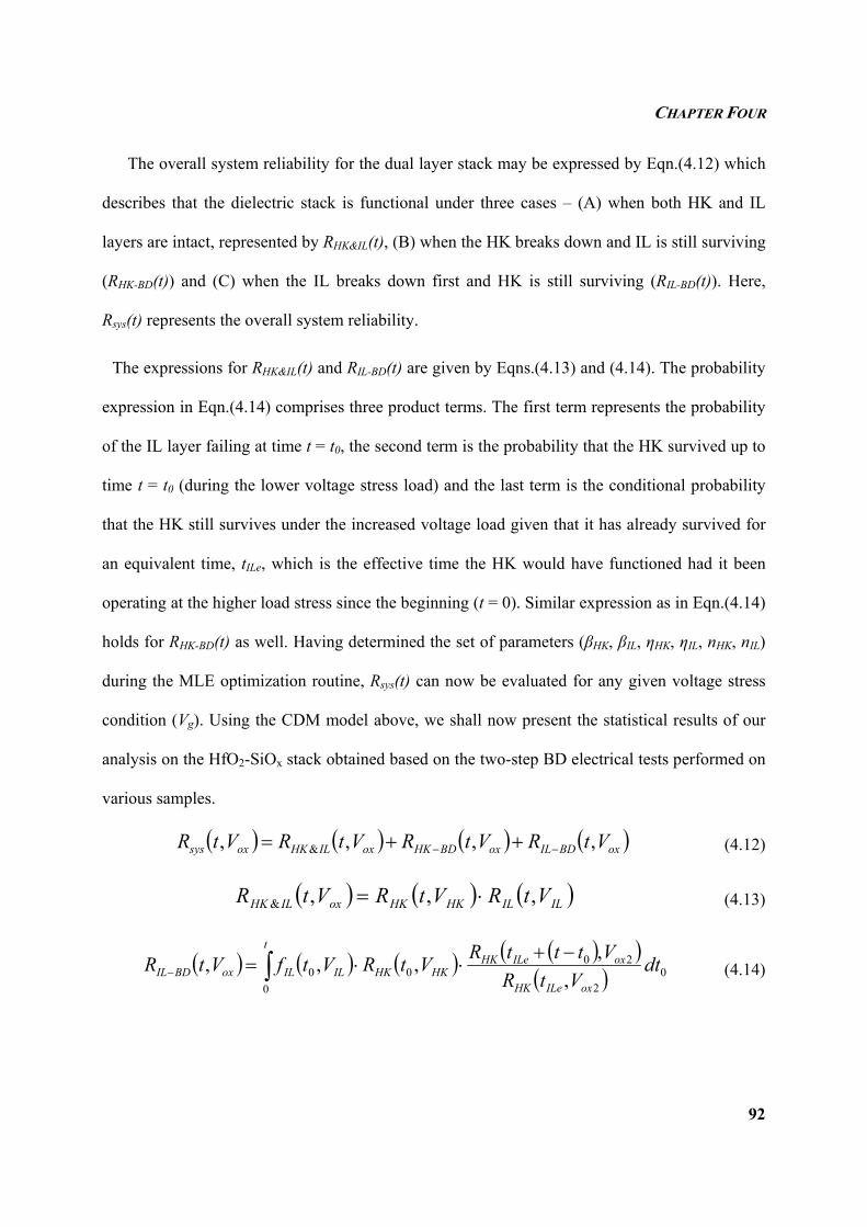
CHAPTER FOUR
92
The overall system reliability for the dual layer stack may be expressed by Eqn.(4.12) which
describes that the dielectric stack is functional under three cases – (A) when both HK and IL
layers are intact, represented by RHK&IL(t), (B) when the HK breaks down and IL is still surviving
(RHK-BD(t)) and (C) when the IL breaks down first and HK is still surviving (RIL-BD(t)). Here,
Rsys(t) represents the overall system reliability.
The expressions for RHK&IL(t) and RIL-BD(t) are given by Eqns.(4.13) and (4.14). The probability
expression in Eqn.(4.14) comprises three product terms. The first term represents the probability
of the IL layer failing at time t = t0, the second term is the probability that the HK survived up to
time t = t0 (during the lower voltage stress load) and the last term is the conditional probability
that the HK still survives under the increased voltage load given that it has already survived for
an equivalent time, tILe, which is the effective time the HK would have functioned had it been
operating at the higher load stress since the beginning (t = 0). Similar expression as in Eqn.(4.14)
holds for RHK-BD(t) as well. Having determined the set of parameters (βHK, βIL, ηHK, ηIL, nHK, nIL)
during the MLE optimization routine, Rsys(t) can now be evaluated for any given voltage stress
condition (Vg). Using the CDM model above, we shall now present the statistical results of our
analysis on the HfO2-SiOx stack obtained based on the two-step BD electrical tests performed on
various samples.
( ) ( ) ( ) ( )oxBDILoxBDHKoxILHKoxsys VtRVtRVtRVtR ,,,, & −− ++= (4.12)
( ) ( ) ( )ILILHKHKoxILHK VtRVtRVtR ,,,& ⋅= (4.13)
( ) ( ) ( ) ( )( )( ) 0
2
2000
0 ,,,,, dt
VtRVtttRVtRVtfVtR
oxILeHK
oxILeHKHKHKIL
t
ILoxBDIL−+
⋅⋅= ∫− (4.14)
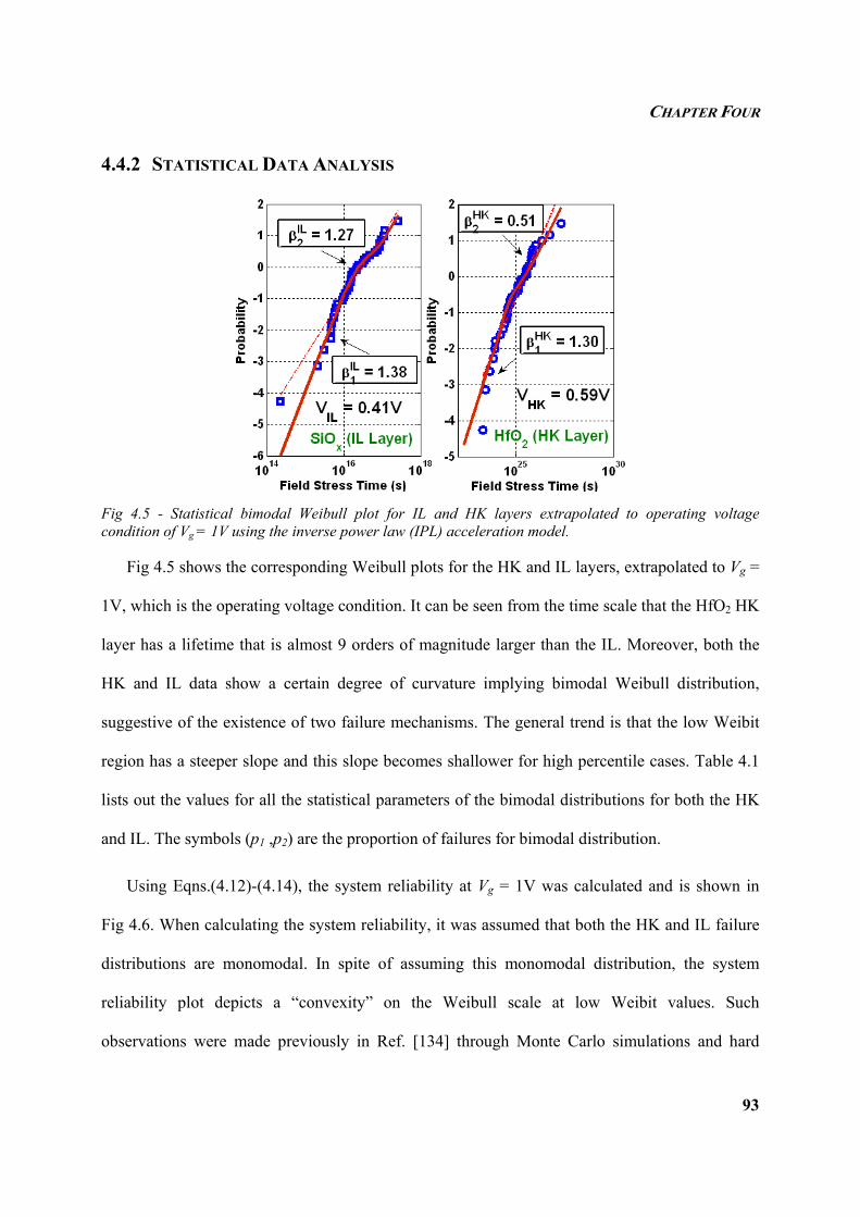
CHAPTER FOUR
93
4.4.2 STATISTICAL DATA ANALYSIS
Fig 4.5 - Statistical bimodal Weibull plot for IL and HK layers extrapolated to operating voltage condition of Vg = 1V using the inverse power law (IPL) acceleration model.
Fig 4.5 shows the corresponding Weibull plots for the HK and IL layers, extrapolated to Vg =
1V, which is the operating voltage condition. It can be seen from the time scale that the HfO2 HK
layer has a lifetime that is almost 9 orders of magnitude larger than the IL. Moreover, both the
HK and IL data show a certain degree of curvature implying bimodal Weibull distribution,
suggestive of the existence of two failure mechanisms. The general trend is that the low Weibit
region has a steeper slope and this slope becomes shallower for high percentile cases. Table 4.1
lists out the values for all the statistical parameters of the bimodal distributions for both the HK
and IL. The symbols (p1 ,p2) are the proportion of failures for bimodal distribution.
Using Eqns.(4.12)-(4.14), the system reliability at Vg = 1V was calculated and is shown in
Fig 4.6. When calculating the system reliability, it was assumed that both the HK and IL failure
distributions are monomodal. In spite of assuming this monomodal distribution, the system
reliability plot depicts a “convexity” on the Weibull scale at low Weibit values. Such
observations were made previously in Ref. [134] through Monte Carlo simulations and hard
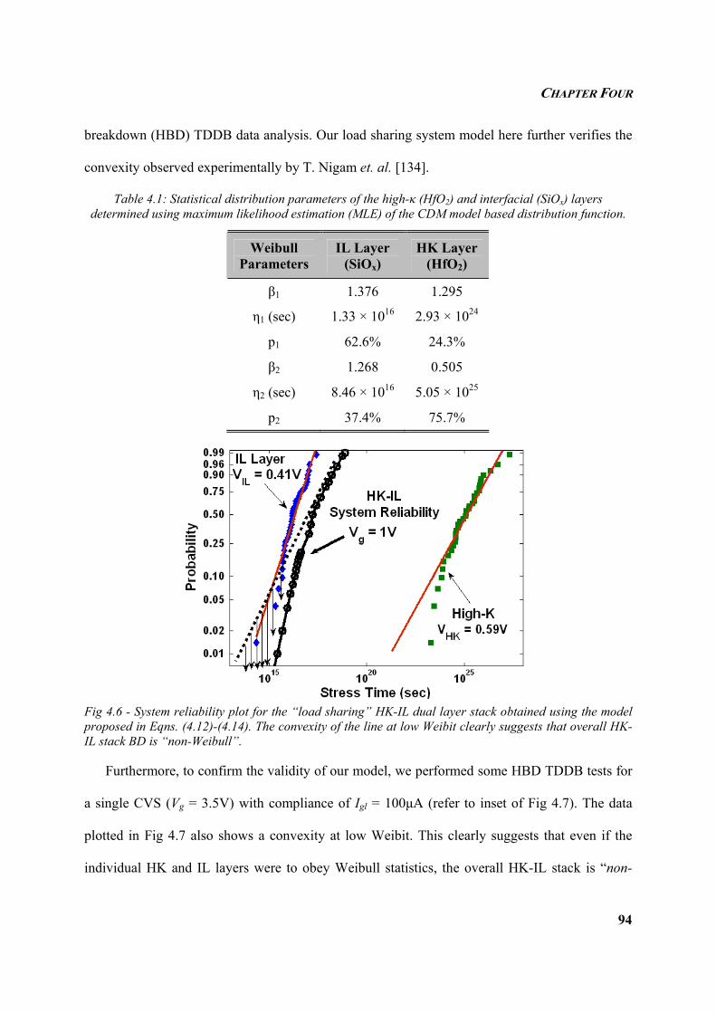
CHAPTER FOUR
94
breakdown (HBD) TDDB data analysis. Our load sharing system model here further verifies the
convexity observed experimentally by T. Nigam et. al. [134].
Table 4.1: Statistical distribution parameters of the high-κ (HfO2) and interfacial (SiOx) layers determined using maximum likelihood estimation (MLE) of the CDM model based distribution function.
Weibull Parameters
IL Layer (SiOx)
HK Layer (HfO2)
β1 1.376 1.295
η1 (sec) 1.33 × 10¹⁶ 2.93 × 1024
p1 62.6% 24.3%
β2 1.268 0.505
η2 (sec) 8.46 × 10¹⁶ 5.05 × 1025
p2 37.4% 75.7%
Fig 4.6 - System reliability plot for the “load sharing” HK-IL dual layer stack obtained using the model proposed in Eqns. (4.12)-(4.14). The convexity of the line at low Weibit clearly suggests that overall HK-IL stack BD is “non-Weibull”.
Furthermore, to confirm the validity of our model, we performed some HBD TDDB tests for
a single CVS (Vg = 3.5V) with compliance of Igl = 100µA (refer to inset of Fig 4.7). The data
plotted in Fig 4.7 also shows a convexity at low Weibit. This clearly suggests that even if the
individual HK and IL layers were to obey Weibull statistics, the overall HK-IL stack is “non-
CHAPTER FOUR
95
Weibull” in nature and has no specific closed form statistical distribution, as can be confirmed by
the complex reliability expressions in Eqns.(4.12)-(4.14). Therefore, use of the conventional
Weibull distribution to fit overall HK-IL stack BD data is statistically inappropriate and could
lead to erroneous reliability projections.
Fig 4.7 - Comparison of the load-sharing HK-IL dependent system model with the HBD data after bi-layer BD at Vg = 3.5V. The close match of the test data and model imply that the model well describes HK-IL failure statistics. Inset shows some of the HBD single stage CVS leakage evolution trends in the bi-layer stack.
The system reliability is again calculated in Fig.4.7 at Vg = 3.5V to compare the model
estimates () with the HBD data ( ). The model and the data fit relatively well suggesting that
the proposed load sharing system model correctly describes the degradation trends of the HK-IL
stack. Some deviations of the model from the data are expected because as mentioned
previously, use of a single stage CVS at Vg = 3.5V may not fully represent the “intrinsic” nature
of failure of the gate stack.
From Table 4.1 and Figs.4.5 and 4.6, it can be seen that the mean lifetime for both the HK
and IL layers is very long, many orders more than the required standard reliability target of 10
CHAPTER FOUR
96
years at operating conditions. All the analysis above is at the “device level” only. It is necessary
to extend these results to the “circuit level” in order to assess whether we are able to meet the
minimum reliability specifications.
A. WEIBULL SLOPE ANALYSIS
Weibull slope (β) is an important parameter, indicative of the number of traps needed to
create a percolation. It is expressed by Eqn.(4.15) where α is the SILC degradation rate, a0 is the
trap radius and NSIT = (tox/a0) represents the number of stress-induced traps (SIT) in the
percolation path [133]. Our new statistical model has enabled us to extract the β values
separately for the HK and IL and additionally the β values for the sub distributions in the
bimodal data. The early failures in both HK and IL have a larger β compared to the wear-out
failures. We speculate this to be a combined effect of a high α and low (tox/a0) since these early
failures are usually “extrinsic” in nature or occur in highly defective devices with a high process-
induced trap (PIT) concentration, thus requiring very few SIT to cause percolation. The term
(tox/a0) in Eqn.(4.15) only corresponds to the SIT, while N represents the overall number of traps
comprising the percolation path.
( )PITSITox NNNat
−•=•=⎟⎟⎠
⎞⎜⎜⎝
⎛⋅= αααβ
0
(4.15)
Table 4.2: Magnitude of the various factors affecting the Weibull slope for the early and wear-out failure mechanisms (FM) in the HK and IL layers.
Failure Mechanism (FM) β α (tox / a0) PIT
HK / IL – FM 1 (Early)
HK / IL – FM 2 (Wear-out)
The wear-out failures which generally show a low β, correspond to a combined effect of low
α and high (tox/a0) since wear-out failures are “intrinsic” and occur in defect-free or low defect
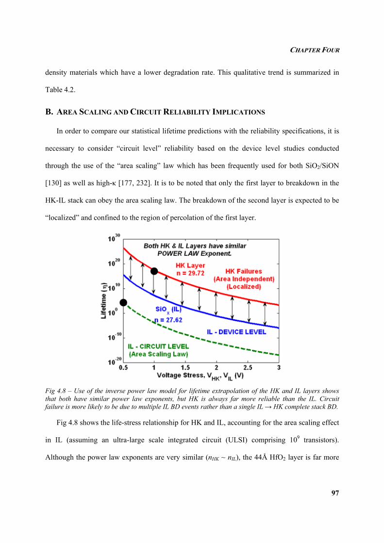
CHAPTER FOUR
97
density materials which have a lower degradation rate. This qualitative trend is summarized in
Table 4.2.
B. AREA SCALING AND CIRCUIT RELIABILITY IMPLICATIONS
In order to compare our statistical lifetime predictions with the reliability specifications, it is
necessary to consider “circuit level” reliability based on the device level studies conducted
through the use of the “area scaling” law which has been frequently used for both SiO2/SiON
[130] as well as high-κ [177, 232]. It is to be noted that only the first layer to breakdown in the
HK-IL stack can obey the area scaling law. The breakdown of the second layer is expected to be
“localized” and confined to the region of percolation of the first layer.
Fig 4.8 – Use of the inverse power law model for lifetime extrapolation of the HK and IL layers shows that both have similar power law exponents, but HK is always far more reliable than the IL. Circuit failure is more likely to be due to multiple IL BD events rather than a single IL → HK complete stack BD.
Fig 4.8 shows the life-stress relationship for HK and IL, accounting for the area scaling effect
in IL (assuming an ultra-large scale integrated circuit (ULSI) comprising 109 transistors).
Although the power law exponents are very similar (nHK ~ nIL), the 44Å HfO2 layer is far more
CHAPTER FOUR
98
reliable than the 8Å IL by many orders of magnitude. Taking into account the area scaling
further reduces the IL reliability very significantly. As shown by the dotted line in Fig 4.8, for Vg
= 1V which corresponds to VIL ~ 0.41V based on Eqns. 3.1 and 3.2, the mean-time-to-failure, η,
for the first IL BD spot is as low as 105 seconds. Subsequent HK failure at the percolated IL
region is improbable as the corresponding η for HK is as high as 1017 seconds (VHK ~ Vop after 1-
layer BD). The two points of reference we talk about here are shown in Fig. 4.8 as black circles.
At the circuit level, it is necessary to deduce whether failure occurs due to multiple IL BD
events only or a sequential HK-IL complete stack BD is plausible. To investigate this, we use the
low percentile Weibull approximation model as given by Eqn. (4.16) [233] to quantify the
lifetime enhancement (χ = TBD-K/TBD-1) due to K multiple BD events, where W = ln(-ln(1-F)) is
the Weibit value corresponding to the percentile failure, F and Weibull slope, β. Considering the
circuit to comprise of 109 transistors, the scale parameter for IL BD is scaled accordingly using
the area scaling rule and the mean time to failure for the first IL BD event at circuit level is as
low as 105 seconds. We calculated the effect of the number of IL SBD events on the lifetime
enhancement factor, χ, as plotted in Fig. 4.9(b) for different standard failure criterion of F = 1, 10
and 100 ppm. An interesting saturation-like trend of χ for K > 50 is observed. This suggests that
low percentile lifetime enhancement becomes less prominent for a large number of multiple BD
events. At high percentiles, it is well known that the improvement in lifetime is less evident for
all multiple BD events [234]. For K > 50 BD events, the maximum lifetime enhancement
possible is of the order of 109 seconds, corresponding to F = 1 ppm.
( )( ) ( )
⎭⎬⎫
⎩⎨⎧
⎟⎟⎠
⎞⎜⎜⎝
⎛ −−⋅==
−
−
βχ β
KKWK
FTFT
K
BD
KBD 1exp!1
1 (4.16)
From the Ig-Vg leakage trends in Fig. 4.9(a) for many devices after IL BD, we expect the
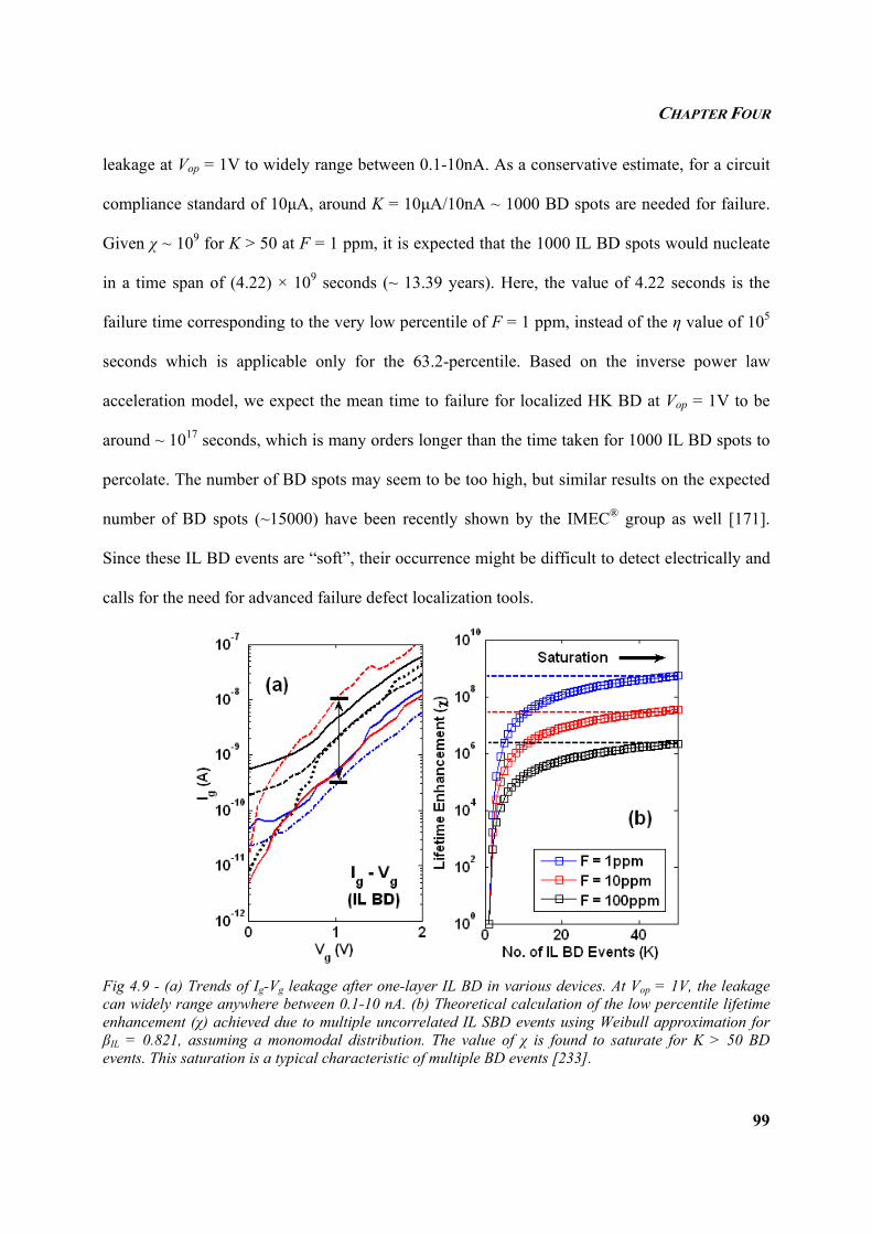
CHAPTER FOUR
99
leakage at Vop = 1V to widely range between 0.1-10nA. As a conservative estimate, for a circuit
compliance standard of 10µA, around K = 10µA/10nA ~ 1000 BD spots are needed for failure.
Given χ ~ 109 for K > 50 at F = 1 ppm, it is expected that the 1000 IL BD spots would nucleate
in a time span of (4.22) × 109 seconds (~ 13.39 years). Here, the value of 4.22 seconds is the
failure time corresponding to the very low percentile of F = 1 ppm, instead of the η value of 105
seconds which is applicable only for the 63.2-percentile. Based on the inverse power law
acceleration model, we expect the mean time to failure for localized HK BD at Vop = 1V to be
around ~ 1017 seconds, which is many orders longer than the time taken for 1000 IL BD spots to
percolate. The number of BD spots may seem to be too high, but similar results on the expected
number of BD spots (~15000) have been recently shown by the IMEC® group as well [171].
Since these IL BD events are “soft”, their occurrence might be difficult to detect electrically and
calls for the need for advanced failure defect localization tools.
Fig 4.9 - (a) Trends of Ig-Vg leakage after one-layer IL BD in various devices. At Vop = 1V, the leakage can widely range anywhere between 0.1-10 nA. (b) Theoretical calculation of the low percentile lifetime enhancement (χ) achieved due to multiple uncorrelated IL SBD events using Weibull approximation for βIL = 0.821, assuming a monomodal distribution. The value of χ is found to saturate for K > 50 BD events. This saturation is a typical characteristic of multiple BD events [233].
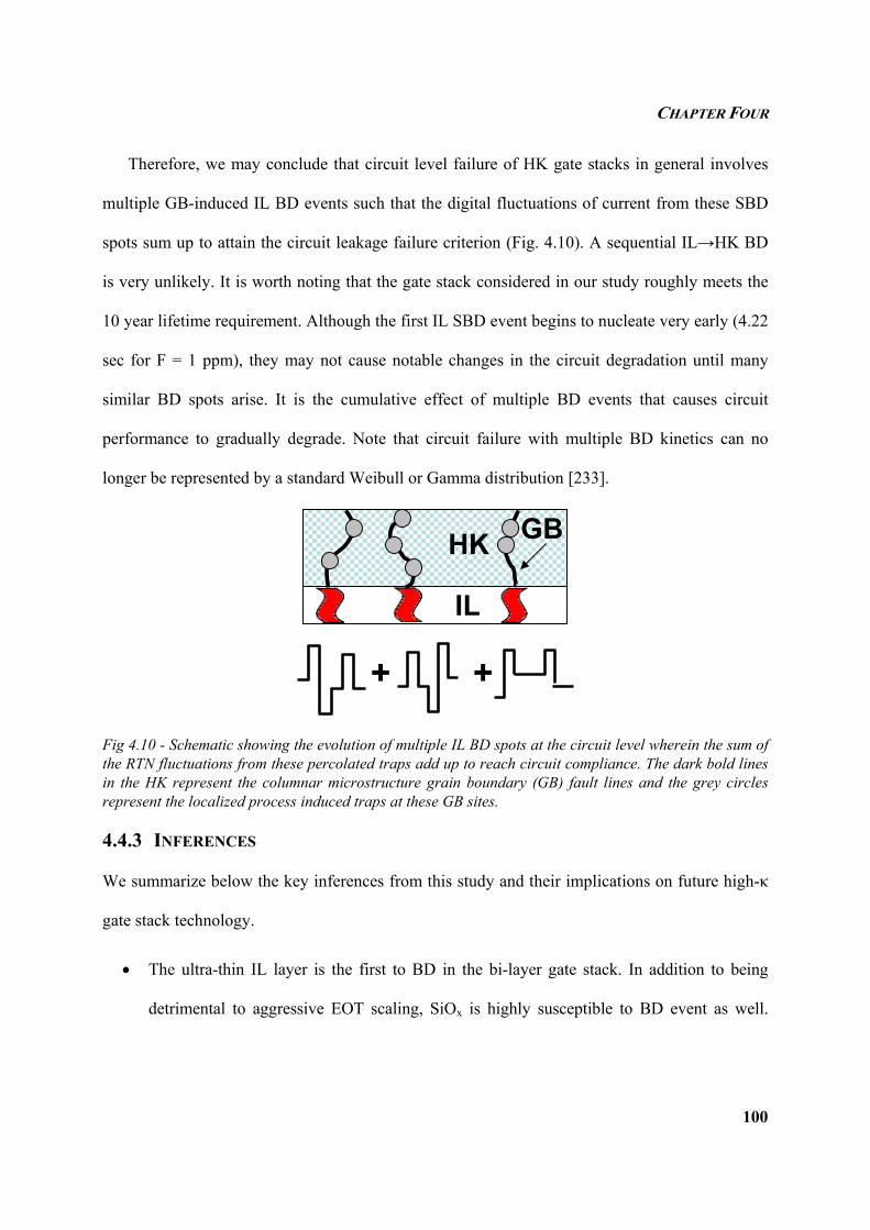
CHAPTER FOUR
100
Therefore, we may conclude that circuit level failure of HK gate stacks in general involves
multiple GB-induced IL BD events such that the digital fluctuations of current from these SBD
spots sum up to attain the circuit leakage failure criterion (Fig. 4.10). A sequential IL→HK BD
is very unlikely. It is worth noting that the gate stack considered in our study roughly meets the
10 year lifetime requirement. Although the first IL SBD event begins to nucleate very early (4.22
sec for F = 1 ppm), they may not cause notable changes in the circuit degradation until many
similar BD spots arise. It is the cumulative effect of multiple BD events that causes circuit
performance to gradually degrade. Note that circuit failure with multiple BD kinetics can no
longer be represented by a standard Weibull or Gamma distribution [233].
Fig 4.10 - Schematic showing the evolution of multiple IL BD spots at the circuit level wherein the sum of the RTN fluctuations from these percolated traps add up to reach circuit compliance. The dark bold lines in the HK represent the columnar microstructure grain boundary (GB) fault lines and the grey circles represent the localized process induced traps at these GB sites.
4.4.3 INFERENCES
We summarize below the key inferences from this study and their implications on future high-κ
gate stack technology.
• The ultra-thin IL layer is the first to BD in the bi-layer gate stack. In addition to being
detrimental to aggressive EOT scaling, SiOx is highly susceptible to BD event as well.
IL
HK GB
+ +
CHAPTER FOUR
101
Since these ultra-thin IL layers are defective sub-oxides (SiOx, x < 2) and only about 2-3
monolayers thick, they show poor robustness to TDDB failures.
• The implementation of a zero-IL (ZIL) solution is questionable from a reliability point of
view since IL serves as a “buffer” to confine BD to a single layer, without causing the HK
to percolate. In the absence of IL, the HK will percolate during BD event (causing high
leakage bridging gate and substrate) and this could occur at a higher rate of trap generation
if the microstructure of the processed HK material is polycrystalline with localized grain
boundary defects.
• Both the HK and IL layers show bimodal statistics in general. In HK, this is likely due to
the stochastic distribution of the number of process induced traps in the grain boundary
which is the weakest link path for early TDDB. In other words, the bimodal trends are
exhibited because there may be some devices with very defective GB containing more PIT
than in the other devices. Amorphous HK materials are likely to exhibit a monomodal
behavior as trap generation is uniform in the absence of GB fault lines.
• Overall gate stack does not obey Weibull statistics. It does not have any closed form
statistical distribution. It is a complex function of many Weibull CDFs. Only at very low
percentile values, use of the Weibull approximation may be partially acceptable.
• It is predicted that circuit level failure occurs only by multiple IL BD events rather than a
sequential IL → HK breakdown.
• The study above only considered a single gate stack consisting of 44Ǻ HfO2 and 8Ǻ SiOx.
It is to be noted that the sequence of BD may heavily depend on the relative thickness of
the HK and IL layers as illustrated in Fig 4.11. Depending on the tHK : tIL ratio and stress
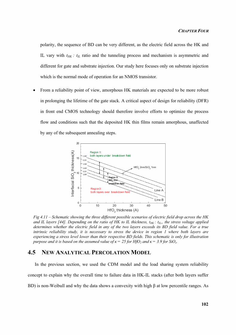
CHAPTER FOUR
102
polarity, the sequence of BD can be very different, as the electric field across the HK and
IL vary with tHK : tIL ratio and the tunneling process and mechanism is asymmetric and
different for gate and substrate injection. Our study here focuses only on substrate injection
which is the normal mode of operation for an NMOS transistor.
• From a reliability point of view, amorphous HK materials are expected to be more robust
in prolonging the lifetime of the gate stack. A critical aspect of design for reliability (DFR)
in front end CMOS technology should therefore involve efforts to optimize the process
flow and conditions such that the deposited HK thin films remain amorphous, unaffected
by any of the subsequent annealing steps.
Fig 4.11 – Schematic showing the three different possible scenarios of electric field drop across the HK and IL layers [44]. Depending on the ratio of HK to IL thickness, tHK : tIL,, the stress voltage applied determines whether the electric field in any of the two layers exceeds its BD field value. For a true intrinsic reliability study, it is necessary to stress the device in region 1 where both layers are experiencing a stress level lower than their respective BD fields. This schematic is only for illustration purpose and it is based on the assumed value of κ = 25 for HfO2 and κ = 3.9 for SiOx.
4.5 NEW ANALYTICAL PERCOLATION MODEL
In the previous section, we used the CDM model and the load sharing system reliability
concept to explain why the overall time to failure data in HK-IL stacks (after both layers suffer
BD) is non-Weibull and why the data shows a convexity with high β at low percentile ranges. As
CHAPTER FOUR
103
for the individual failure data trend for the HK, we documented it to also follow a bimodal trend
with different trap generation rates for the low and high percentile ranges. However, we have
still not found the root cause for the convexity in the HK failure data plot. In this section, we
identify the pitfalls of conventional percolation models and propose a new analytical model that
accounts for the microstructural variations in HK thin films and explains this observed convexity.
The focus of this section is purely on the HK layer only. In other words, we assume a zero-IL
condition here and focus on the trap generation kinetics within the HK-layer. To our knowledge,
this is one of the first studies that explains the non-Weibull trend based on our strong physical
evidence of non-uniform trap generation kinetics in the HK using STM analysis [78].
4.5.1 EARLIER PERCOLATION MODELS
We briefly look at the derivation of the conventional percolation model [133] first.
Considering a 2D cell diagram as in Fig. 4.12 where every cell represents a trap (defect),
accounting for the possibility of non-columnar percolation paths, there are 3n-1 possible
combinations of paths nucleating from any particular bottom cell as reference, where n = tox/a0 is
the number of cell rows (indicative of the oxide thickness). The percolation probability (Fperc) at
any specific bottom cell can therefore be expressed by Eqn. (4.17) [133] where λ is the time-
dependent probability that any random cell is defective (or equivalently it is the fraction of
defective cells in the entire lattice).
nnpercF λ⋅= −13 (4.17)
Using this expression, the overall reliability (probability of no percolation path being formed)
can be given by Eqn. (4.18) where FBD is the breakdown probability. This can be expressed in a
linearized Weibull form as given by Eqn. (4.19), making use of the Taylor’s series
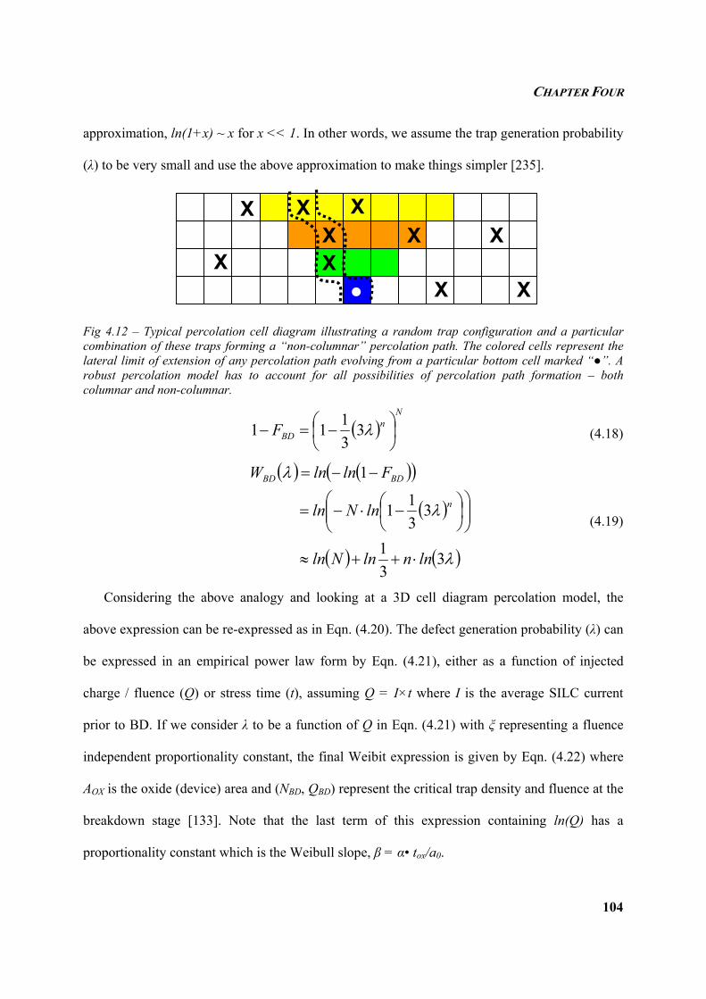
CHAPTER FOUR
104
approximation, ln(1+x) ~ x for x << 1. In other words, we assume the trap generation probability
(λ) to be very small and use the above approximation to make things simpler [235].
Fig 4.12 – Typical percolation cell diagram illustrating a random trap configuration and a particular combination of these traps forming a “non-columnar” percolation path. The colored cells represent the lateral limit of extension of any percolation path evolving from a particular bottom cell marked “”. A robust percolation model has to account for all possibilities of percolation path formation – both columnar and non-columnar.
( )N
nBDF ⎟
⎠⎞
⎜⎝⎛ −=− λ3
3111 (4.18)
( ) ( )( )
( )
( ) ( )λ
λ
λ
331
3311
1
lnnlnNln
lnNln
FlnlnW
n
BDBD
⋅++≈
⎟⎟⎠
⎞⎜⎜⎝
⎛⎟⎠⎞
⎜⎝⎛ −⋅−=
−−=
(4.19)
Considering the above analogy and looking at a 3D cell diagram percolation model, the
above expression can be re-expressed as in Eqn. (4.20). The defect generation probability (λ) can
be expressed in an empirical power law form by Eqn. (4.21), either as a function of injected
charge / fluence (Q) or stress time (t), assuming Q = I×t where I is the average SILC current
prior to BD. If we consider λ to be a function of Q in Eqn. (4.21) with ξ representing a fluence
independent proportionality constant, the final Weibit expression is given by Eqn. (4.22) where
AOX is the oxide (device) area and (NBD, QBD) represent the critical trap density and fluence at the
breakdown stage [133]. Note that the last term of this expression containing ln(Q) has a
proportionality constant which is the Weibull slope, β = α• tox/a0.
X
XX
XX
X X
XX
X
CHAPTER FOUR
105
( ) ( ) 200
20
551
aAN;ln
atln
aAlnW OXoxOX
BD =⋅++⎟⎟⎠
⎞⎜⎜⎝
⎛= λλ (4.20)
( ) ( ) ααααα ξξξξλ ttIItQ ' ⋅≡⋅⋅=⋅=⋅= (4.21)
( ) ( )Qlnat
QtaNln
at
aAlnQW ox
BDox
BDoxOXBD ⋅⎟⎟
⎠
⎞⎜⎜⎝
⎛⋅+⎟⎟
⎠
⎞⎜⎜⎝
⎛⋅+⎟⎟
⎠
⎞⎜⎜⎝
⎛=
0
30
020
55
αα (4.22)
The above formulation is the complete proof for the conventional analytical percolation
model which states that the β value linearly depends on tox and it is indicative of the number of
traps constituting a percolation path. The extracted β value from accelerated stress tests can be
used to find out the trap size and number of traps using the equation β = α• tox/a0. There are two
important assumptions in the derivation above. One is that we assume the trap generation
probability (λ) to be very small, which may be true for an oxide during the initial stage of stress.
However, for defective dielectrics such as the high-κ and closer to the instant of the breakdown
event, this assumption may not hold true anymore. The second assumption is that we use a power
law to represent λ as a monotonic increasing function of time t. This power law expression is
again valid only for the initial duration of stress. As more traps are created and probability of the
TDDB event increases, considering the limited amount of traps (cells) available for causing
oxide damage, a more accurate expression for λ should reflect the saturation of this probability
for devices with prolonged time to failure [236] because any probability function cannot exceed
its maximum value of 1. When the above assumptions are invalid, the derivation of the simple
expression for the Weibull slope, β = α• tox/a0 is no longer possible.
When the dielectric contains a lot of random process induced traps (PIT) prior to stressing
(more so in the case of high-κ gate stacks), the Weibit function (WBD) can be derived to be
represented by Eqn. (4.23) [133], assuming for simplicity a maximum of one trap in any vertical
CHAPTER FOUR
106
percolative column. Here, R is the number of columns with PIT = 1 and (N-R) is the remaining
number of columns with PIT = 0. This equation clearly shows that the simple linearized
relationship of WBD and Q no longer holds true. Instead, the Weibit line is a complex non-linear
function. This basic derivation here lends initial support to our previous statistical failure data
plot for the HK in Fig. 4.5 where a convexity was observed, indicative of non-Weibull
stochastics.
( ) ( ) ( )[ ]αξα QRNRlnQlnatQW ox
BD ⋅⋅−++⋅⎟⎟⎠
⎞⎜⎜⎝
⎛−⋅= 1
0 (4.23)
Given the various assumptions in existing analytical percolation models and considering the
non-uniform trap generation in HK dielectric films due to the polycrystalline microstructure, it is
imperative to develop a more robust and generic model that can account for these non-ideal
effects and better explain the statistical trend of failure data observed. The following sub-sections
are precisely dedicated to this motive.
4.5.2 PROPOSED PERCOLATION MODEL
Microstructure of HK thin films in advanced gate dielectric stacks plays a major role in
determining the BD statistics, Weibull slope and TDDB lifetime of logic and memory devices.
The grain boundaries (GB) in a polycrystalline HK stack, which are quite often present as a result
of high temperature deposition or subsequent annealing steps, have been shown to cause early
percolation as confirmed by recent STM [237] and TEM investigations [238]. These GB paths
serve as low resistance bridges connecting the gate and substrate due to high localized process
induced trap (PIT) concentration resulting from inter-grain orientation mismatch. Current
percolation models for HK gate stack [133, 236] generally consider defect generation to be
uniform across the device active area. Given the presence of a Gaussian distribution of grain sizes
CHAPTER FOUR
107
in polycrystalline HK films (with a mean diameter of 25 nm as confirmed by STM and TEM
studies) [237], defect generation becomes non-random and is expected to be enhanced around GB
fault lines. Therefore, it is necessary to modify the existing percolation model to account for the
stochastics of this non-random defect generation process and its effect on HK BD statistics and
lifetime distribution. The objective of the study here is to propose such an analytical cell-based
percolation model and quantitatively analyze the effect of defect generation rate (ξ), stress
induced leakage current (SILC) power law exponent (α), device dimension (L), oxide thickness
(tox) and PIT density on the HK BD Weibull plot.
Fig 4.13(a) shows a 2D cellular schematic of the HK dielectric with trap size (a0), length (L)
and mean grain size (d0). For simplicity, we consider grain boundaries (colored columnar cells)
to be uniformly distributed, separated by d0, where d0 >> tox. This is equivalent to simulating the
case of a random grain size distribution for large device dimensions. There are N = (L / a0)
columns and n = (tox/a0) rows in the cell structure. The width of the GB (aGB) is assumed equal to
a0, which is a good assumption as reported in [74]. Moreover, we model the GB to be vertically
aligned (columnar microstructure), ignoring interaction and intersection of different GB lines. As
in most percolation models, we consider each cell in the bottom most layer and the possible
permutations of percolation paths that can evolve from this cell to account for all percolation
configurations across the dielectric. We analyze separately the cells originating from the grain
(bulk) denoted here as “G”, grain boundary, denoted as “GB” and nearest neighbor cells “NN”
that are adjacent to the GB. For a cell structure consisting of n rows, there are 2·(n-1) nearest
neighbor cells through which the bulk and GB traps can interact. Table 4.3 lists out the possible
permutations of G and GB traps for n = 3 and n = 4 in the NN bulk and GB cells.
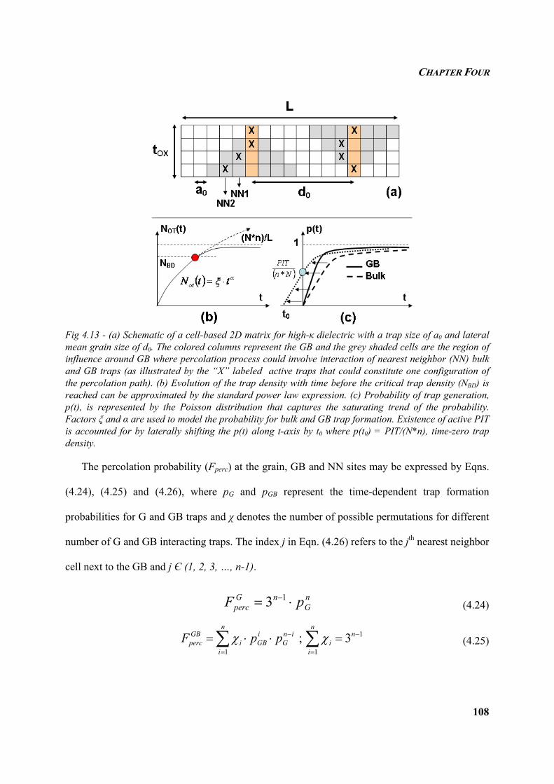
CHAPTER FOUR
108
Fig 4.13 - (a) Schematic of a cell-based 2D matrix for high-κ dielectric with a trap size of a0 and lateral mean grain size of d0. The colored columns represent the GB and the grey shaded cells are the region of influence around GB where percolation process could involve interaction of nearest neighbor (NN) bulk and GB traps (as illustrated by the “X” labeled active traps that could constitute one configuration of the percolation path). (b) Evolution of the trap density with time before the critical trap density (NBD) is reached can be approximated by the standard power law expression. (c) Probability of trap generation, p(t), is represented by the Poisson distribution that captures the saturating trend of the probability. Factors ξ and α are used to model the probability for bulk and GB trap formation. Existence of active PIT is accounted for by laterally shifting the p(t) along t-axis by t0 where p(t0) = PIT/(N*n), time-zero trap density.
The percolation probability (Fperc) at the grain, GB and NN sites may be expressed by Eqns.
(4.24), (4.25) and (4.26), where pG and pGB represent the time-dependent trap formation
probabilities for G and GB traps and χ denotes the number of possible permutations for different
number of G and GB interacting traps. The index j in Eqn. (4.26) refers to the jth nearest neighbor
cell next to the GB and j Є (1, 2, 3, …, n-1).
nG
nGperc pF ⋅= −13 (4.24)
1
113; −
==
− =⋅⋅= ∑∑ nn
ii
n
i
inG
iGBi
GBperc ppF χχ (4.25)
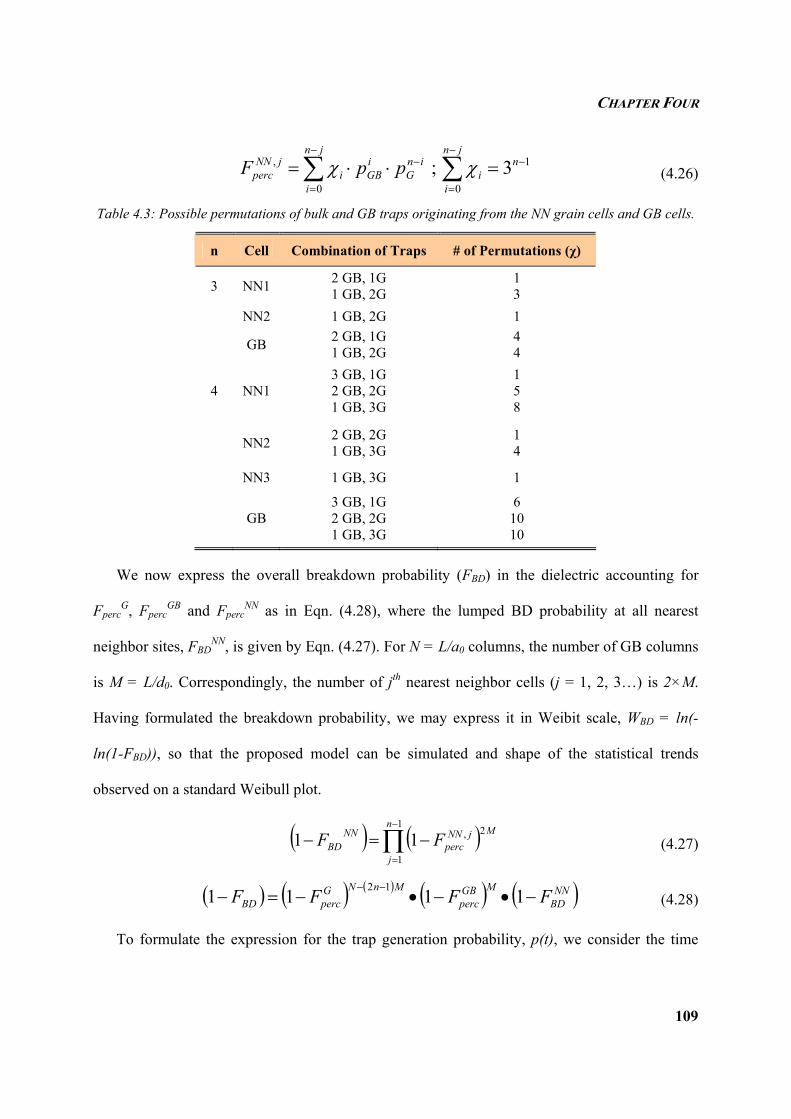
CHAPTER FOUR
109
1
00
, 3; −−
=
−
=
− =⋅⋅= ∑∑ njn
ii
jn
i
inG
iGBi
jNNperc ppF χχ (4.26)
Table 4.3: Possible permutations of bulk and GB traps originating from the NN grain cells and GB cells.
n Cell Combination of Traps # of Permutations (χ)
3 NN1 2 GB, 1G 1 GB, 2G
1 3
NN2 1 GB, 2G 1
GB 2 GB, 1G 1 GB, 2G
4 4
4 NN1 3 GB, 1G 2 GB, 2G 1 GB, 3G
1 5 8
NN2 2 GB, 2G 1 GB, 3G
1 4
NN3 1 GB, 3G 1
GB 3 GB, 1G 2 GB, 2G 1 GB, 3G
6 10 10
We now express the overall breakdown probability (FBD) in the dielectric accounting for
FpercG, Fperc
GB and FpercNN as in Eqn. (4.28), where the lumped BD probability at all nearest
neighbor sites, FBDNN, is given by Eqn. (4.27). For N = L/a0 columns, the number of GB columns
is M = L/d0. Correspondingly, the number of jth nearest neighbor cells (j = 1, 2, 3…) is 2×M.
Having formulated the breakdown probability, we may express it in Weibit scale, WBD = ln(-
ln(1-FBD)), so that the proposed model can be simulated and shape of the statistical trends
observed on a standard Weibull plot.
( ) ( )∏−
=
−=−1
1
2,11n
j
MjNNperc
NNBD FF (4.27)
( ) ( ) ( ) ( ) ( )NNBD
MGBperc
MnNGpercBD FFFF −•−•−=−
−− 1111 12 (4.28)
To formulate the expression for the trap generation probability, p(t), we consider the time
CHAPTER FOUR
110
evolution of oxide trap density (Not) during SILC degradation, which follows a typical empirical
power law (Not = ξ · tα) prior to reaching critical defect density, NBD, (Fig 4.13(b)) where ξ is the
trap generation rate (TGR) which is a strong exponential function of the stress voltage, Vg, while
α, the time exponent, is stress independent [239]. Using Poisson statistics with mean number of
defects per cell = a03 · ξ · tα, the general form of expression for p(t) can be expressed as in Eqn.
(4.29) [236]. Parameters ξ and α are expected to be different for grain and GB regions (Fig
4.13(c)).
( ) ( )αξ tatp ⋅−−= 30exp1 (4.29)
Based on the proposed model, we shall examine the impact of various parameters on BD
distribution and the role of bulk and GB percolation. Unlike previous models, due to the
complexity of Eqn. (4.29), an explicit closed-form expression for Weibull slope (β) dependence
on tox is no longer possible.
4.5.3 SIMULATION RESULTS AND DISCUSSION
The separate contribution of the GB and G cells and G-GB interaction in the NN cells is
illustrated in Fig 4.14(a). Note the unique shape of the distribution curves. While failure at purely
bulk sites is a straight line following Weibull stochastics (analogous to early percolation models),
GB sites show a convex trend and the NN cells exhibit a bimodal trend where the low percentile
region follows GB failure, while high percentile cases tend towards the ideal distribution of bulk
failure. The overall trend (WBD) seems to be fully governed by the GB failures only and this
clearly points to the dominance of GB-assisted BD in HK gate stacks. We choose realistic values
for the parameters in this simulation as follows → αG = 0.30, αGB = 0.35, L = 65nm, n = 4, ξG = 1
× 1014 cm-3s-0.3, ξGB = 1 × 1015 cm-3s-0.35, a0 = 8Ǻ and d0 = 25nm. From Fig 4.14(b), the first
CHAPTER FOUR
111
nearest neighbor to the GB cell plays a significant role in the BD, while the second and third NN
cells show BD distribution trends closer to bulk failures.
Fig 4.14(c) supports the need for using the proposed model here to represent HK layer failure
data. The uniform TGR model cannot describe the convexity in the electrical failure data as
observed in the Weibull plot (refer to Fig 4.14(h)). Only the non-uniform TGR model with
different G-GB degradation trends is able to reproduce the experimental failure trends. We use
the non-columnar model here which allows us to consider the possibility of traps from adjacent
columns constituting a non-vertical “slanted” (non-columnar) percolation path. This is more
realistic and allows us to model the G-GB interactions. In Fig 4.14(d), very low dimensions of 22
nm show curvilinear trends while large area samples show a straight line. This is because, in
large samples, when the possibility of competitive failure at the large number of GB sites is
accounted for, the overall failure distribution “approximates” well to Weibull stochastics. Note
that in all cases, GB failures clearly dominate the failure distribution.
Fig 4.14(e) shows the effect of the ratio (ξGB / ξG) on the BD trends. Only when ξGB : ξG >
10:1 is a clear convexity in the Weibull trends observed. Since the HK BD experimental data in
Fig 4.14(h) show this trend, it clearly points to the orders of magnitude higher TGR at GB sites.
Similarly, convex Weibull trends are seen in Fig 4.14(f) when (αGB - αG) > 0. It is however not
very feasible to extract the separate values of αGB and αG from experiments and therefore, for all
practical cases, they can be assumed to be equal. Fig 4.14(g) shows the effect of oxide thickness
(n = tox/a0) where the low percentile trends show a large shift with increasing n, while the
distributions tend to merge at the high percentile range. This suggests that the thickness
advantage for longer TDDB lifetime is not very significant if the HK microstructure consists of
GB. For a high concentration of as-deposited PIT (0.3%), note that the tail of the distribution
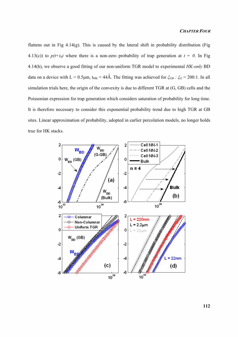
CHAPTER FOUR
112
flattens out in Fig 4.14(g). This is caused by the lateral shift in probability distribution (Fig
4.13(c)) to p(t+t0) where there is a non-zero probability of trap generation at t = 0. In Fig
4.14(h), we observe a good fitting of our non-uniform TGR model to experimental HK-only BD
data on a device with L = 0.5µm, tHK = 44Ǻ. The fitting was achieved for ξGB : ξG = 200:1. In all
simulation trials here, the origin of the convexity is due to different TGR at (G, GB) cells and the
Poissonian expression for trap generation which considers saturation of probability for long time.
It is therefore necessary to consider this exponential probability trend due to high TGR at GB
sites. Linear approximation of probability, adopted in earlier percolation models, no longer holds
true for HK stacks.
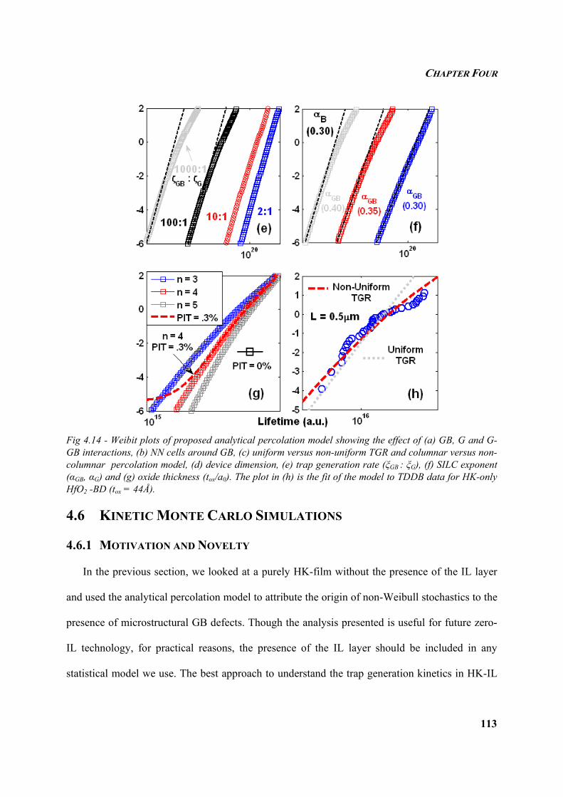
CHAPTER FOUR
113
Fig 4.14 - Weibit plots of proposed analytical percolation model showing the effect of (a) GB, G and G-GB interactions, (b) NN cells around GB, (c) uniform versus non-uniform TGR and columnar versus non-columnar percolation model, (d) device dimension, (e) trap generation rate (ξGB : ξG), (f) SILC exponent (αGB, αG) and (g) oxide thickness (tox/a0). The plot in (h) is the fit of the model to TDDB data for HK-only HfO2 -BD (tox = 44Å).
4.6 KINETIC MONTE CARLO SIMULATIONS
4.6.1 MOTIVATION AND NOVELTY
In the previous section, we looked at a purely HK-film without the presence of the IL layer
and used the analytical percolation model to attribute the origin of non-Weibull stochastics to the
presence of microstructural GB defects. Though the analysis presented is useful for future zero-
IL technology, for practical reasons, the presence of the IL layer should be included in any
statistical model we use. The best approach to understand the trap generation kinetics in HK-IL
CHAPTER FOUR
114
stacks is to “simulate” the process using Kinetic Monte Carlo (KMC) techniques [240, 241] and
analyze the distribution of simulated times to failure. In order for the simulation to match the
actual trap generation kinetics, we have to use thermochemical models that can describe the rate
of trap generation as a physical function of the accelerating factors – electric field (ξ) and
temperature (T).
There have been noteworthy efforts in the recent past to simulate the HK-IL failure statistics
using the KMC routine by Nigam et. al. [134]; however the analysis has a few critical drawbacks.
The first is that the expression for the trap generation rate (TGR) was assumed to follow an
empirical power law, based on the general trend of leakage current increase in the SILC pre-
TDDB stage. It did not account for the physics-based dependence of TGR on (ξ, T) considering
the fundamental phenomenon of oxygen vacancy generation. Fitting of the model to
experimental data was achieved by free variation of the parameters. However, it was not
analyzed whether the values of these parameters that fitted the test data were realistic from a
theoretical physics perspective. The second drawback is that their work did not decode the
individual failure distributions of the HK and IL. Rather, they only simulated the final time to
failure of the complete HK-IL stack. It was also not clear whether their model accounted for the
increased stress across the surviving HK layer, after the IL layer broke down first. The model
also does not account for the microstructural effects in the HK (role of grain boundaries) as well.
Considering these limitations, it was necessary to address these issues in the process of
developing a more holistic and robust KMC model for HK-IL breakdown.
4.6.2 CHEMISTRY OF TRAP GENERATION
As discussed in Section 2.2.4, the chemical nature of dielectric breakdown involves
generation of oxygen vacancies which originate from the bond breaking process of Hf-O (HK) or
CHAPTER FOUR
115
Si-O (IL) bonds depending on the material. Therefore, to model the trap generation process, we
have to focus on the bond breaking chemical reaction rate (k), which can be expressed in a
general form by Eqn. (4.30) [242], where Ea, p0, κ, ν and kB refer to the field-free activation
energy for bond breaking, molecular dipole moment, relative permittivity, lattice (structural)
vibrational frequency and Boltzmann constant respectively. The term p0 • (2+κ)/3 is collectively
referred to as the “bond polarization factor”. The second term in the numerator within the
exponential factor refers to the reduction of the activation energy barrier for bond breaking when
voltage / electric field is applied, resulting in a lower effective value of Ea-eff. The values for the
various parameters of this model are listed in Table 4.4, many of which have been extracted from
various literature reports [52, 242-244]. Since the values for the localized permittivity at the GB
and post-BD IL regions have not been documented previously, we assume reasonable values
(slightly higher than the intrinsic material permittivity) for κBULK and κIL-BD, indicative of their
higher oxygen deficiency. This is based on reports [245, 246] that correlate oxygen deficiency in
a HK film to an increase in its permittivity.
( )⎟⎟⎠
⎞⎜⎜⎝
⎛−⋅=⎟⎟
⎠
⎞⎜⎜⎝
⎛ ⋅+⋅−−⋅= −
TkE
expTk
/pEexpkB
effa
B
a νξκν 32 (4.30)
4.6.3 KINETIC MONTE CARLO ROUTINE
Fig. 4.15 shows the detailed flowchart of the KMC routine adopted in this study. For
simplicity, we take a 2D percolation model with columnar percolation paths. This is to avoid the
use of complex cluster identification algorithms (such as Hoshen-Kopelman method [247])
which could end up being computationally intensive. Initially, we start with trap generation in
the HK and IL layers separately and find the time to break down for each of them. We then
identify the smaller of the two (denoted here as TBD1), i.e., we find out whether HK or the IL is
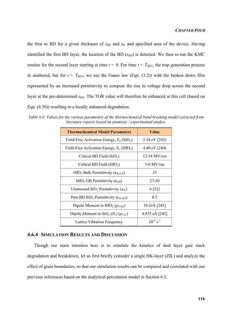
CHAPTER FOUR
116
the first to BD for a given thickness of tHK and tIL and specified area of the device. Having
identified the first BD layer, the location of the BD (sBD) is detected. We then re-run the KMC
routine for the second layer starting at time t = 0. For time t < TBD1, the trap generation process
in unaltered, but for t > TBD1, we use the Gauss law (Eqn. (3.2)) with the broken down film
represented by an increased permittivity to compute the rise in voltage drop across the second
layer at the pre-determined sBD. The TGR value will therefore be enhanced at this cell (based on
Eqn. (4.30)) resulting in a locally enhanced degradation.
Table 4.4: Values for the various parameters of the thermochemical bond breaking model extracted from literature reports based on atomistic / experimental studies.
Thermochemical Model Parameters Value
Field-Free Activation Energy, Ea (SiOx) 2.34 eV [242]
Field-Free Activation Energy, Ea (HfO2) 4.40 eV [244]
Critical BD Field (SiOx) 12-18 MV/cm
Critical BD Field (HfO2) 5-6 MV/cm
HfO2 Bulk Permittivity (κBULK) 25
HfO2 GB Permittivity (κGB) 27-30
Unstressed SiOx Permittivity (κIL) 6 [52]
Post BD SiOx Permittivity (κIL-BD) 8.5
Dipole Moment in HfO2 (p0-HK) 10.2eǺ [243]
Dipole Moment in SiOx (IL) (p0-IL) 4.875 eǺ [242]
Lattice Vibration Frequency 1013 s-1
4.6.4 SIMULATION RESULTS AND DISCUSSION
Though our main intention here is to simulate the kinetics of dual layer gate stack
degradation and breakdown, let us first briefly consider a single HK-layer (ZIL) and analyze the
effect of grain boundaries, so that our simulation results can be compared and correlated with our
previous inferences based on the analytical percolation model in Section 4.5.
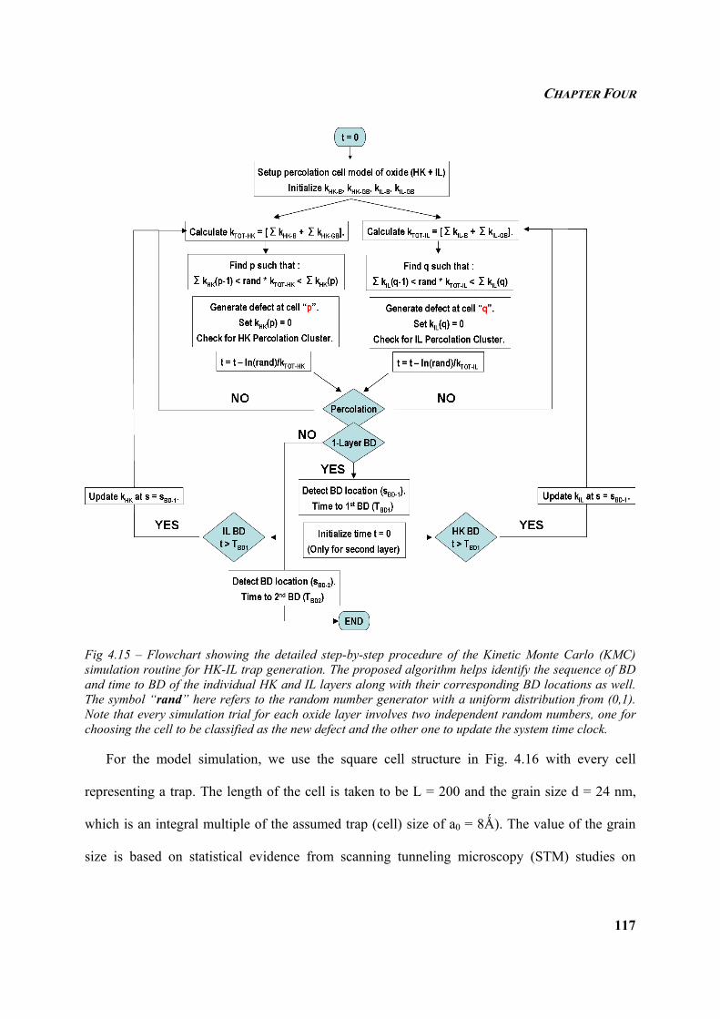
CHAPTER FOUR
117
Fig 4.15 – Flowchart showing the detailed step-by-step procedure of the Kinetic Monte Carlo (KMC) simulation routine for HK-IL trap generation. The proposed algorithm helps identify the sequence of BD and time to BD of the individual HK and IL layers along with their corresponding BD locations as well. The symbol “rand” here refers to the random number generator with a uniform distribution from (0,1). Note that every simulation trial for each oxide layer involves two independent random numbers, one for choosing the cell to be classified as the new defect and the other one to update the system time clock.
For the model simulation, we use the square cell structure in Fig. 4.16 with every cell
representing a trap. The length of the cell is taken to be L = 200 and the grain size d = 24 nm,
which is an integral multiple of the assumed trap (cell) size of a0 = 8Ǻ). The value of the grain
size is based on statistical evidence from scanning tunneling microscopy (STM) studies on
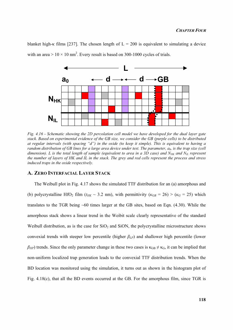
CHAPTER FOUR
118
blanket high-κ films [237]. The chosen length of L = 200 is equivalent to simulating a device
with an area > 10 × 10 nm2. Every result is based on 300-1000 cycles of trials.
Fig. 4.16 - Schematic showing the 2D percolation cell model we have developed for the dual layer gate stack. Based on experimental evidence of the GB size, we consider the GB (purple cells) to be distributed at regular intervals (with spacing “d”) in the oxide (to keep it simple). This is equivalent to having a random distribution of GB lines for a large area device under test. The parameter, a0, is the trap size (cell dimension). L is the total length of sample (equivalent to area in a 3D case) and NHK and NIL represent the number of layers of HK and IL in the stack. The grey and red cells represent the process and stress induced traps in the oxide respectively.
A. ZERO INTERFACIAL LAYER STACK
The Weibull plot in Fig. 4.17 shows the simulated TTF distribution for an (a) amorphous and
(b) polycrystalline HfO2 film (tHK ~ 3.2 nm), with permittivity (κGB = 26) > (κG = 25) which
translates to the TGR being ~60 times larger at the GB sites, based on Eqn. (4.30). While the
amorphous stack shows a linear trend in the Weibit scale clearly representative of the standard
Weibull distribution, as is the case for SiO2 and SiON, the polycrystalline microstructure shows
convexial trends with steeper low percentile (higher βLP) and shallower high percentile (lower
βHP) trends. Since the only parameter change in these two cases is κGB ≠ κG, it can be implied that
non-uniform localized trap generation leads to the convexial TTF distribution trends. When the
BD location was monitored using the simulation, it turns out as shown in the histogram plot of
Fig. 4.18(c), that all the BD events occurred at the GB. For the amorphous film, since TGR is
La0 d
NHK
NIL
GB d
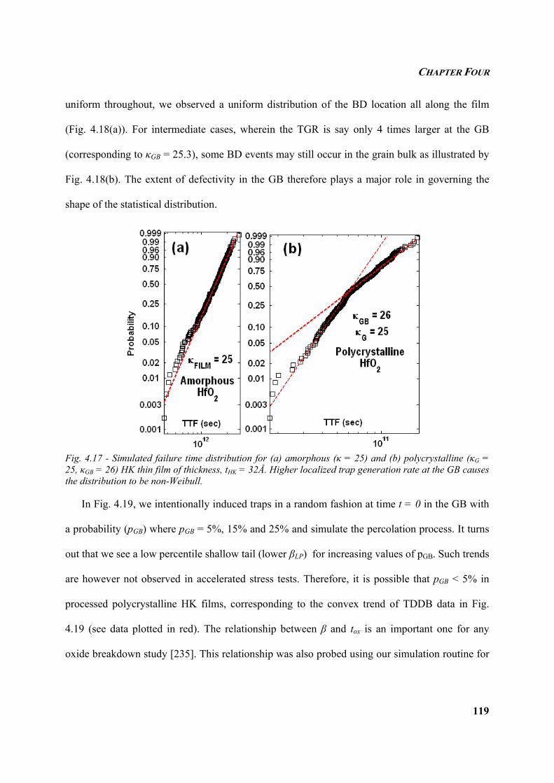
CHAPTER FOUR
119
uniform throughout, we observed a uniform distribution of the BD location all along the film
(Fig. 4.18(a)). For intermediate cases, wherein the TGR is say only 4 times larger at the GB
(corresponding to κGB = 25.3), some BD events may still occur in the grain bulk as illustrated by
Fig. 4.18(b). The extent of defectivity in the GB therefore plays a major role in governing the
shape of the statistical distribution.
Fig. 4.17 - Simulated failure time distribution for (a) amorphous (κ = 25) and (b) polycrystalline (κG = 25, κGB = 26) HK thin film of thickness, tHK = 32Å. Higher localized trap generation rate at the GB causes the distribution to be non-Weibull.
In Fig. 4.19, we intentionally induced traps in a random fashion at time t = 0 in the GB with
a probability (pGB) where pGB = 5%, 15% and 25% and simulate the percolation process. It turns
out that we see a low percentile shallow tail (lower βLP) for increasing values of pGB. Such trends
are however not observed in accelerated stress tests. Therefore, it is possible that pGB < 5% in
processed polycrystalline HK films, corresponding to the convex trend of TDDB data in Fig.
4.19 (see data plotted in red). The relationship between β and tox is an important one for any
oxide breakdown study [235]. This relationship was also probed using our simulation routine for
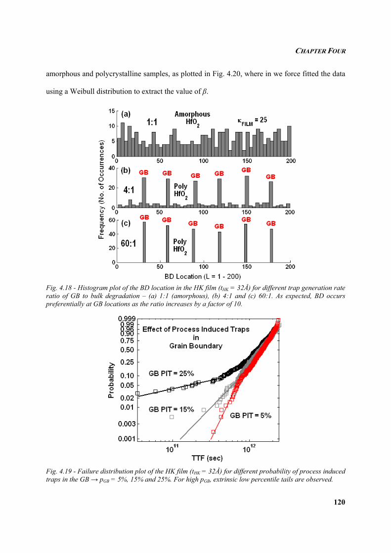
CHAPTER FOUR
120
amorphous and polycrystalline samples, as plotted in Fig. 4.20, where in we force fitted the data
using a Weibull distribution to extract the value of β.
Fig. 4.18 - Histogram plot of the BD location in the HK film (tHK = 32Å) for different trap generation rate ratio of GB to bulk degradation – (a) 1:1 (amorphous), (b) 4:1 and (c) 60:1. As expected, BD occurs preferentially at GB locations as the ratio increases by a factor of 10.
Fig. 4.19 - Failure distribution plot of the HK film (tHK = 32Å) for different probability of process induced traps in the GB → pGB = 5%, 15% and 25%. For high pGB, extrinsic low percentile tails are observed.
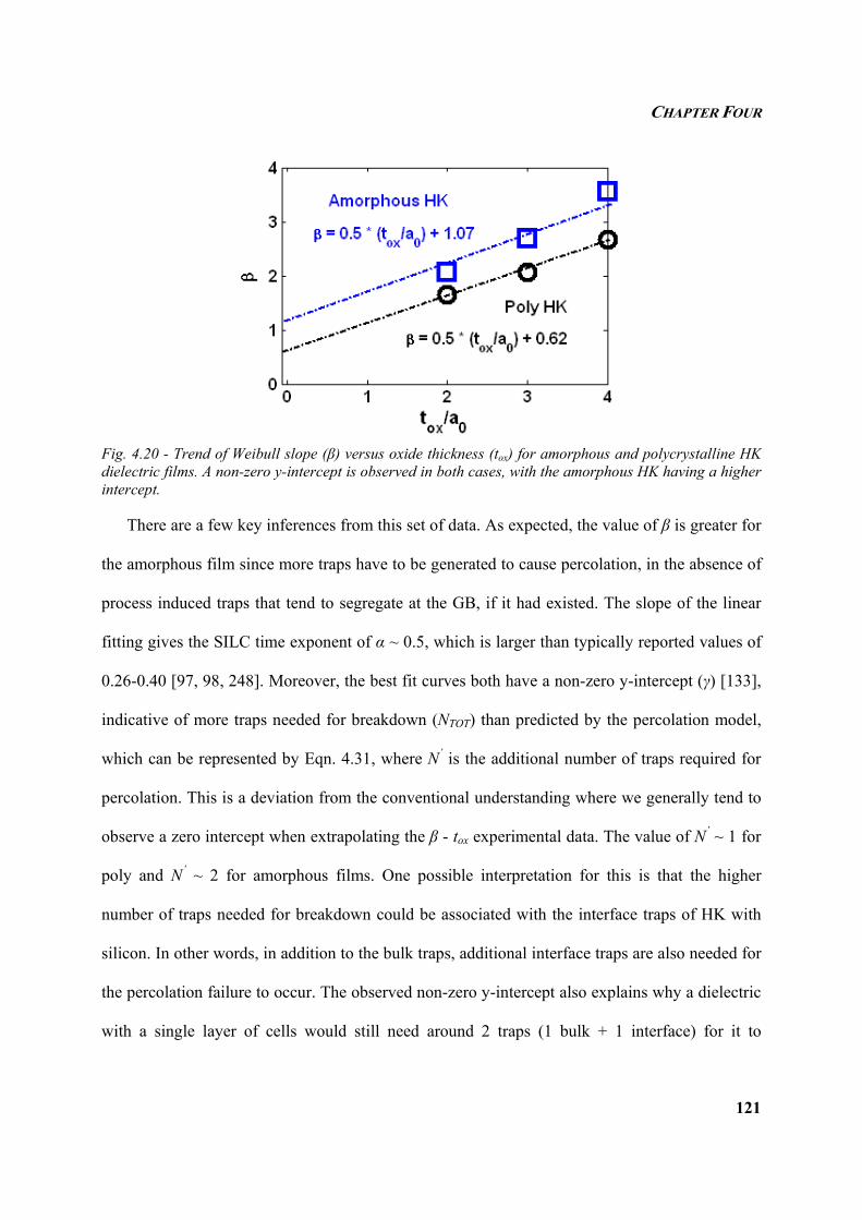
CHAPTER FOUR
121
Fig. 4.20 - Trend of Weibull slope (β) versus oxide thickness (tox) for amorphous and polycrystalline HK dielectric films. A non-zero y-intercept is observed in both cases, with the amorphous HK having a higher intercept.
There are a few key inferences from this set of data. As expected, the value of β is greater for
the amorphous film since more traps have to be generated to cause percolation, in the absence of
process induced traps that tend to segregate at the GB, if it had existed. The slope of the linear
fitting gives the SILC time exponent of α ~ 0.5, which is larger than typically reported values of
0.26-0.40 [97, 98, 248]. Moreover, the best fit curves both have a non-zero y-intercept (γ) [133],
indicative of more traps needed for breakdown (NTOT) than predicted by the percolation model,
which can be represented by Eqn. 4.31, where N’ is the additional number of traps required for
percolation. This is a deviation from the conventional understanding where we generally tend to
observe a zero intercept when extrapolating the β - tox experimental data. The value of N’ ~ 1 for
poly and N’ ~ 2 for amorphous films. One possible interpretation for this is that the higher
number of traps needed for breakdown could be associated with the interface traps of HK with
silicon. In other words, in addition to the bulk traps, additional interface traps are also needed for
the percolation failure to occur. The observed non-zero y-intercept also explains why a dielectric
with a single layer of cells would still need around 2 traps (1 bulk + 1 interface) for it to
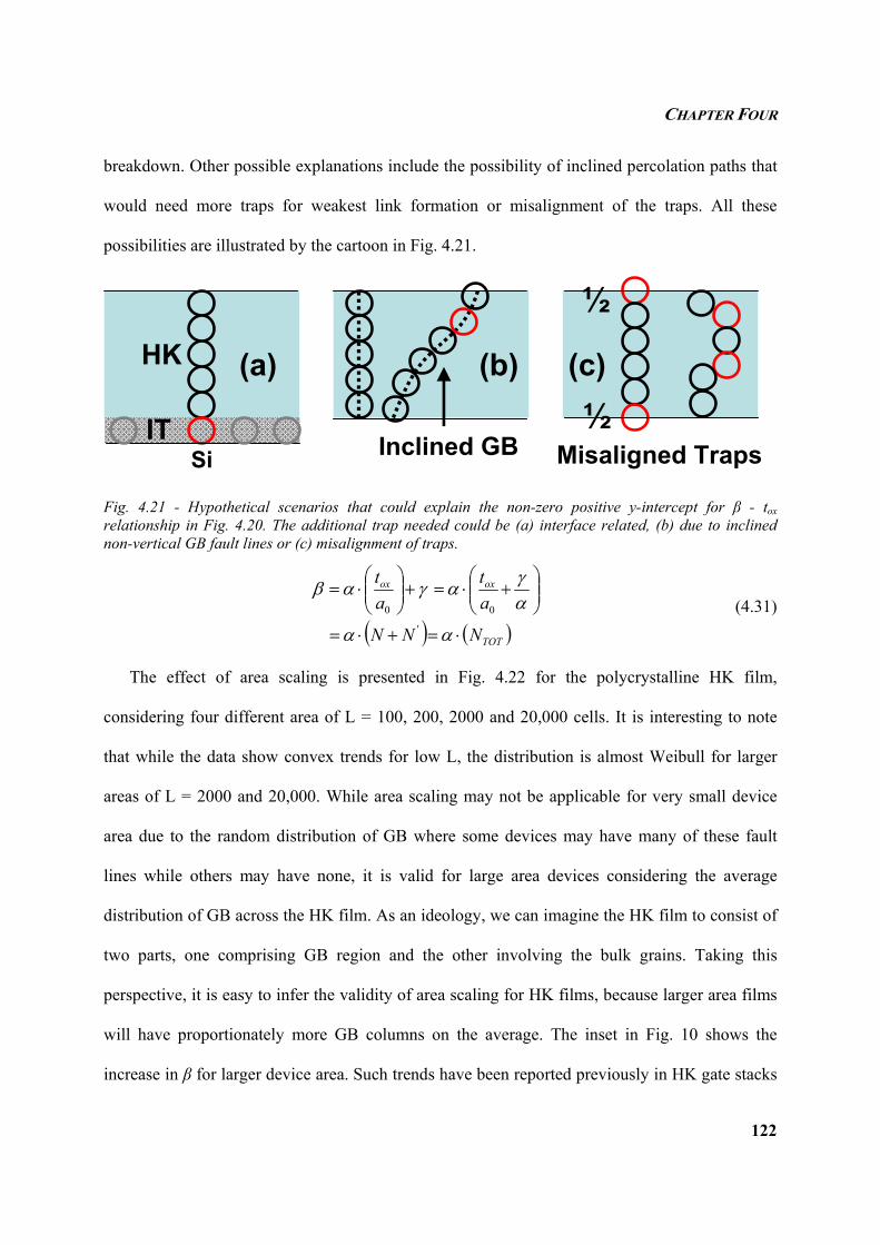
CHAPTER FOUR
122
breakdown. Other possible explanations include the possibility of inclined percolation paths that
would need more traps for weakest link formation or misalignment of the traps. All these
possibilities are illustrated by the cartoon in Fig. 4.21.
Fig. 4.21 - Hypothetical scenarios that could explain the non-zero positive y-intercept for β - tox relationship in Fig. 4.20. The additional trap needed could be (a) interface related, (b) due to inclined non-vertical GB fault lines or (c) misalignment of traps.
( ) ( )TOT'
oxox
NNN
at
at
⋅=+⋅=
⎟⎟⎠
⎞⎜⎜⎝
⎛+⋅=+⎟⎟
⎠
⎞⎜⎜⎝
⎛⋅=
αα
αγαγαβ
00 (4.31)
The effect of area scaling is presented in Fig. 4.22 for the polycrystalline HK film,
considering four different area of L = 100, 200, 2000 and 20,000 cells. It is interesting to note
that while the data show convex trends for low L, the distribution is almost Weibull for larger
areas of L = 2000 and 20,000. While area scaling may not be applicable for very small device
area due to the random distribution of GB where some devices may have many of these fault
lines while others may have none, it is valid for large area devices considering the average
distribution of GB across the HK film. As an ideology, we can imagine the HK film to consist of
two parts, one comprising GB region and the other involving the bulk grains. Taking this
perspective, it is easy to infer the validity of area scaling for HK films, because larger area films
will have proportionately more GB columns on the average. The inset in Fig. 10 shows the
increase in β for larger device area. Such trends have been reported previously in HK gate stacks
½
½IT
HK
Si Inclined GB Misaligned Traps
(a) (b) (c)
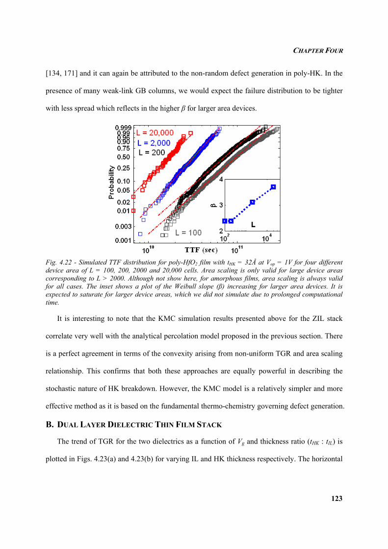
CHAPTER FOUR
123
[134, 171] and it can again be attributed to the non-random defect generation in poly-HK. In the
presence of many weak-link GB columns, we would expect the failure distribution to be tighter
with less spread which reflects in the higher β for larger area devices.
Fig. 4.22 - Simulated TTF distribution for poly-HfO2 film with tHK = 32Å at Vop = 1V for four different device area of L = 100, 200, 2000 and 20,000 cells. Area scaling is only valid for large device areas corresponding to L > 2000. Although not show here, for amorphous films, area scaling is always valid for all cases. The inset shows a plot of the Weibull slope (β) increasing for larger area devices. It is expected to saturate for larger device areas, which we did not simulate due to prolonged computational time.
It is interesting to note that the KMC simulation results presented above for the ZIL stack
correlate very well with the analytical percolation model proposed in the previous section. There
is a perfect agreement in terms of the convexity arising from non-uniform TGR and area scaling
relationship. This confirms that both these approaches are equally powerful in describing the
stochastic nature of HK breakdown. However, the KMC model is a relatively simpler and more
effective method as it is based on the fundamental thermo-chemistry governing defect generation.
B. DUAL LAYER DIELECTRIC THIN FILM STACK
The trend of TGR for the two dielectrics as a function of Vg and thickness ratio (tHK : tIL) is
plotted in Figs. 4.23(a) and 4.23(b) for varying IL and HK thickness respectively. The horizontal
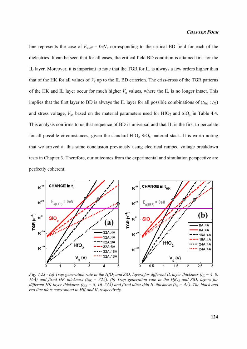
CHAPTER FOUR
124
line represents the case of Ea-eff = 0eV, corresponding to the critical BD field for each of the
dielectrics. It can be seen that for all cases, the critical field BD condition is attained first for the
IL layer. Moreover, it is important to note that the TGR for IL is always a few orders higher than
that of the HK for all values of Vg up to the IL BD criterion. The criss-cross of the TGR patterns
of the HK and IL layer occur for much higher Vg values, where the IL is no longer intact. This
implies that the first layer to BD is always the IL layer for all possible combinations of (tHK : tIL)
and stress voltage, Vg, based on the material parameters used for HfO2 and SiOx in Table 4.4.
This analysis confirms to us that sequence of BD is universal and that IL is the first to percolate
for all possible circumstances, given the standard HfO2-SiOx material stack. It is worth noting
that we arrived at this same conclusion previously using electrical ramped voltage breakdown
tests in Chapter 3. Therefore, our outcomes from the experimental and simulation perspective are
perfectly coherent.
Fig. 4.23 - (a) Trap generation rate in the HfO2 and SiOx layers for different IL layer thickness (tIL = 4, 8, 16Å) and fixed HK thickness (tHK = 32Å). (b) Trap generation rate in the HfO2 and SiOx layers for different HK layer thickness (tHK = 8, 16, 24Å) and fixed ultra-thin IL thickness (tIL = 4Å). The black and red line plots correspond to HK and IL respectively.
(a)(b)
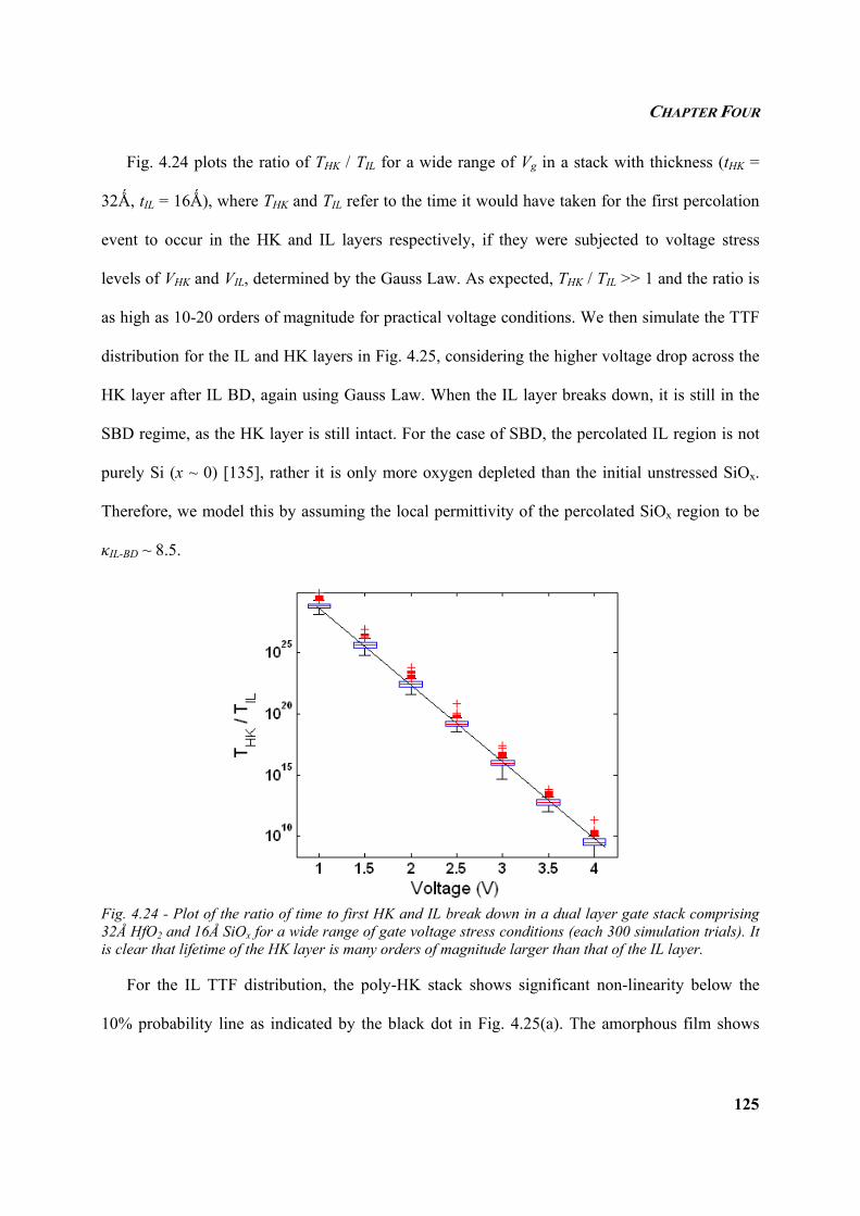
CHAPTER FOUR
125
Fig. 4.24 plots the ratio of THK / TIL for a wide range of Vg in a stack with thickness (tHK =
32Ǻ, tIL = 16Ǻ), where THK and TIL refer to the time it would have taken for the first percolation
event to occur in the HK and IL layers respectively, if they were subjected to voltage stress
levels of VHK and VIL, determined by the Gauss Law. As expected, THK / TIL >> 1 and the ratio is
as high as 10-20 orders of magnitude for practical voltage conditions. We then simulate the TTF
distribution for the IL and HK layers in Fig. 4.25, considering the higher voltage drop across the
HK layer after IL BD, again using Gauss Law. When the IL layer breaks down, it is still in the
SBD regime, as the HK layer is still intact. For the case of SBD, the percolated IL region is not
purely Si (x ~ 0) [135], rather it is only more oxygen depleted than the initial unstressed SiOx.
Therefore, we model this by assuming the local permittivity of the percolated SiOx region to be
κIL-BD ~ 8.5.
Fig. 4.24 - Plot of the ratio of time to first HK and IL break down in a dual layer gate stack comprising 32Å HfO2 and 16Å SiOx for a wide range of gate voltage stress conditions (each 300 simulation trials). It is clear that lifetime of the HK layer is many orders of magnitude larger than that of the IL layer.
For the IL TTF distribution, the poly-HK stack shows significant non-linearity below the
10% probability line as indicated by the black dot in Fig. 4.25(a). The amorphous film shows
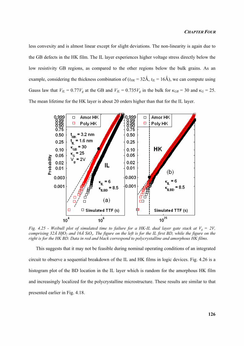
CHAPTER FOUR
126
less convexity and is almost linear except for slight deviations. The non-linearity is again due to
the GB defects in the HK film. The IL layer experiences higher voltage stress directly below the
low resistivity GB regions, as compared to the other regions below the bulk grains. As an
example, considering the thickness combination of (tHK = 32Ǻ, tIL = 16Ǻ), we can compute using
Gauss law that VIL = 0.77Vg at the GB and VIL = 0.735Vg in the bulk for κGB = 30 and κG = 25.
The mean lifetime for the HK layer is about 20 orders higher than that for the IL layer.
Fig. 4.25 - Weibull plot of simulated time to failure for a HK-IL dual layer gate stack at Vg = 2V, comprising 32Å HfO2 and 16Å SiOx. The figure on the left is for the IL first BD, while the figure on the right is for the HK BD. Data in red and black correspond to polycrystalline and amorphous HK films.
This suggests that it may not be feasible during nominal operating conditions of an integrated
circuit to observe a sequential breakdown of the IL and HK films in logic devices. Fig. 4.26 is a
histogram plot of the BD location in the IL layer which is random for the amorphous HK film
and increasingly localized for the polycrystalline microstructure. These results are similar to that
presented earlier in Fig. 4.18.
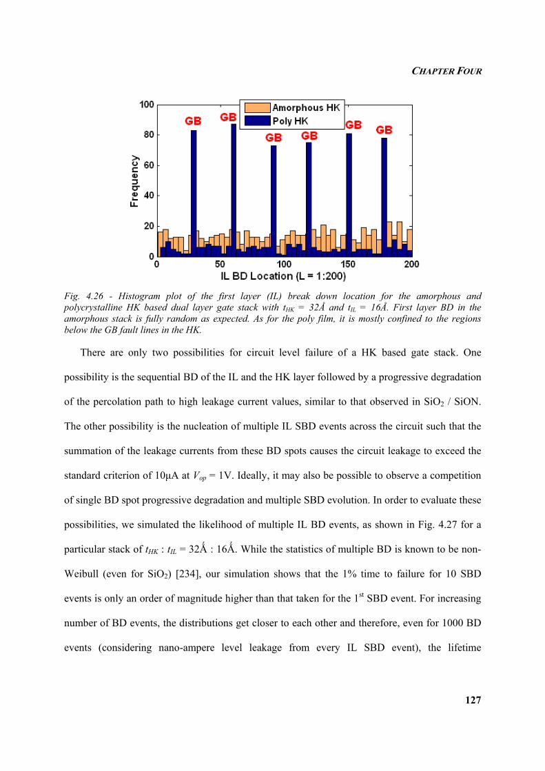
CHAPTER FOUR
127
Fig. 4.26 - Histogram plot of the first layer (IL) break down location for the amorphous and polycrystalline HK based dual layer gate stack with tHK = 32Å and tIL = 16Å. First layer BD in the amorphous stack is fully random as expected. As for the poly film, it is mostly confined to the regions below the GB fault lines in the HK.
There are only two possibilities for circuit level failure of a HK based gate stack. One
possibility is the sequential BD of the IL and the HK layer followed by a progressive degradation
of the percolation path to high leakage current values, similar to that observed in SiO2 / SiON.
The other possibility is the nucleation of multiple IL SBD events across the circuit such that the
summation of the leakage currents from these BD spots causes the circuit leakage to exceed the
standard criterion of 10µA at Vop = 1V. Ideally, it may also be possible to observe a competition
of single BD spot progressive degradation and multiple SBD evolution. In order to evaluate these
possibilities, we simulated the likelihood of multiple IL BD events, as shown in Fig. 4.27 for a
particular stack of tHK : tIL = 32Ǻ : 16Ǻ. While the statistics of multiple BD is known to be non-
Weibull (even for SiO2) [234], our simulation shows that the 1% time to failure for 10 SBD
events is only an order of magnitude higher than that taken for the 1st SBD event. For increasing
number of BD events, the distributions get closer to each other and therefore, even for 1000 BD
events (considering nano-ampere level leakage from every IL SBD event), the lifetime
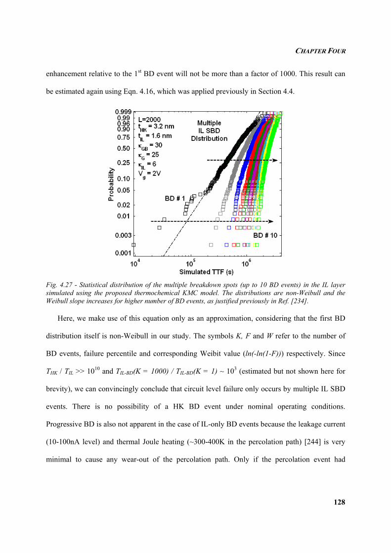
CHAPTER FOUR
128
enhancement relative to the 1st BD event will not be more than a factor of 1000. This result can
be estimated again using Eqn. 4.16, which was applied previously in Section 4.4.
Fig. 4.27 - Statistical distribution of the multiple breakdown spots (up to 10 BD events) in the IL layer simulated using the proposed thermochemical KMC model. The distributions are non-Weibull and the Weibull slope increases for higher number of BD events, as justified previously in Ref. [234].
Here, we make use of this equation only as an approximation, considering that the first BD
distribution itself is non-Weibull in our study. The symbols K, F and W refer to the number of
BD events, failure percentile and corresponding Weibit value (ln(-ln(1-F))) respectively. Since
THK / TIL >> 1010 and TIL-BD(K = 1000) / TIL-BD(K = 1) ~ 103 (estimated but not shown here for
brevity), we can convincingly conclude that circuit level failure only occurs by multiple IL SBD
events. There is no possibility of a HK BD event under nominal operating conditions.
Progressive BD is also not apparent in the case of IL-only BD events because the leakage current
(10-100nA level) and thermal Joule heating (~300-400K in the percolation path) [244] is very
minimal to cause any wear-out of the percolation path. Only if the percolation event had
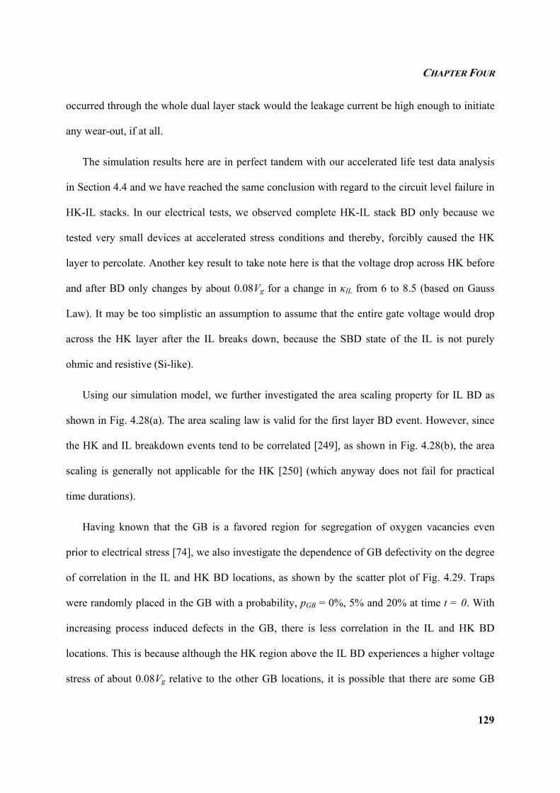
CHAPTER FOUR
129
occurred through the whole dual layer stack would the leakage current be high enough to initiate
any wear-out, if at all.
The simulation results here are in perfect tandem with our accelerated life test data analysis
in Section 4.4 and we have reached the same conclusion with regard to the circuit level failure in
HK-IL stacks. In our electrical tests, we observed complete HK-IL stack BD only because we
tested very small devices at accelerated stress conditions and thereby, forcibly caused the HK
layer to percolate. Another key result to take note here is that the voltage drop across HK before
and after BD only changes by about 0.08Vg for a change in κIL from 6 to 8.5 (based on Gauss
Law). It may be too simplistic an assumption to assume that the entire gate voltage would drop
across the HK layer after the IL breaks down, because the SBD state of the IL is not purely
ohmic and resistive (Si-like).
Using our simulation model, we further investigated the area scaling property for IL BD as
shown in Fig. 4.28(a). The area scaling law is valid for the first layer BD event. However, since
the HK and IL breakdown events tend to be correlated [249], as shown in Fig. 4.28(b), the area
scaling is generally not applicable for the HK [250] (which anyway does not fail for practical
time durations).
Having known that the GB is a favored region for segregation of oxygen vacancies even
prior to electrical stress [74], we also investigate the dependence of GB defectivity on the degree
of correlation in the IL and HK BD locations, as shown by the scatter plot of Fig. 4.29. Traps
were randomly placed in the GB with a probability, pGB = 0%, 5% and 20% at time t = 0. With
increasing process induced defects in the GB, there is less correlation in the IL and HK BD
locations. This is because although the HK region above the IL BD experiences a higher voltage
stress of about 0.08Vg relative to the other GB locations, it is possible that there are some GB
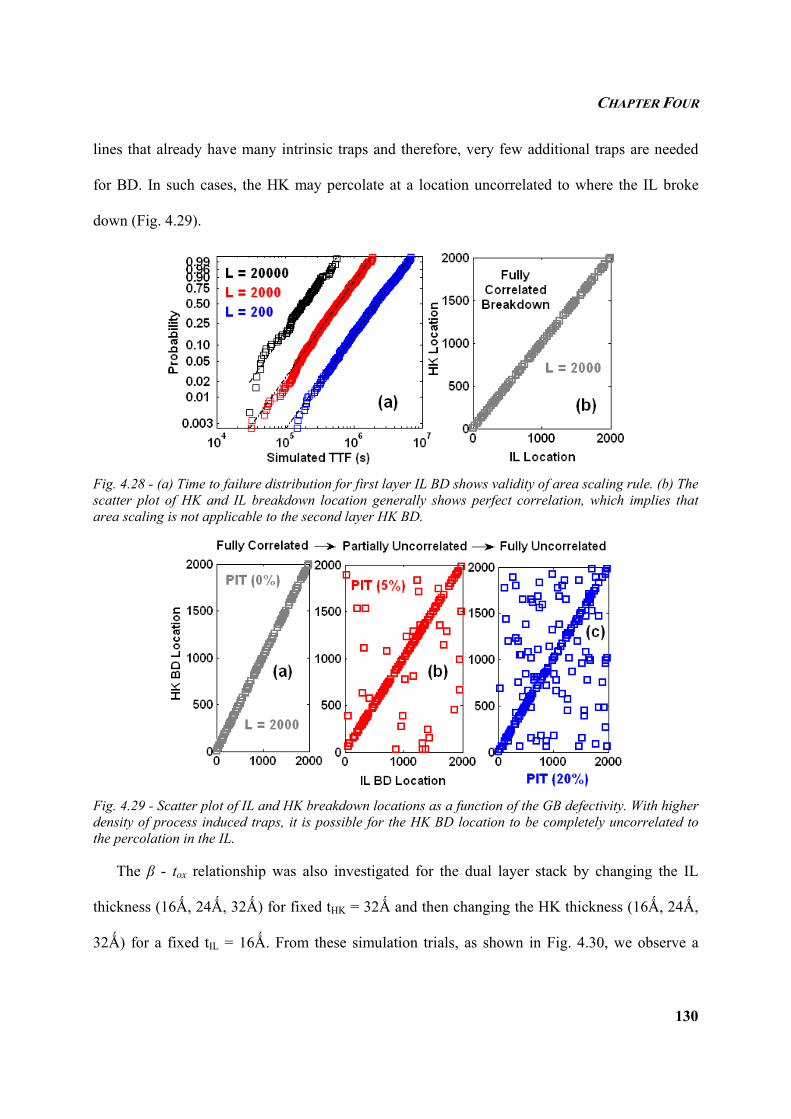
CHAPTER FOUR
130
lines that already have many intrinsic traps and therefore, very few additional traps are needed
for BD. In such cases, the HK may percolate at a location uncorrelated to where the IL broke
down (Fig. 4.29).
Fig. 4.28 - (a) Time to failure distribution for first layer IL BD shows validity of area scaling rule. (b) The scatter plot of HK and IL breakdown location generally shows perfect correlation, which implies that area scaling is not applicable to the second layer HK BD.
Fig. 4.29 - Scatter plot of IL and HK breakdown locations as a function of the GB defectivity. With higher density of process induced traps, it is possible for the HK BD location to be completely uncorrelated to the percolation in the IL.
The β - tox relationship was also investigated for the dual layer stack by changing the IL
thickness (16Ǻ, 24Ǻ, 32Ǻ) for fixed tHK = 32Ǻ and then changing the HK thickness (16Ǻ, 24Ǻ,
32Ǻ) for a fixed tIL = 16Ǻ. From these simulation trials, as shown in Fig. 4.30, we observe a
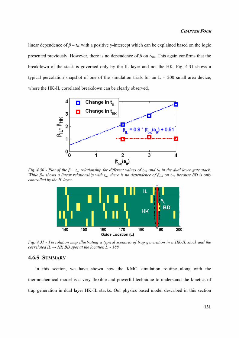
CHAPTER FOUR
131
linear dependence of β – tIL with a positive y-intercept which can be explained based on the logic
presented previously. However, there is no dependence of β on tHK. This again confirms that the
breakdown of the stack is governed only by the IL layer and not the HK. Fig. 4.31 shows a
typical percolation snapshot of one of the simulation trials for an L = 200 small area device,
where the HK-IL correlated breakdown can be clearly observed.
Fig. 4.30 - Plot of the β – tox relationship for different values of tHK and tIL in the dual layer gate stack. While βIL shows a linear relationship with tIL, there is no dependence of βHK on tHK because BD is only controlled by the IL layer.
Fig. 4.31 - Percolation map illustrating a typical scenario of trap generation in a HK-IL stack and the correlated IL → HK BD spot at the location L ~ 188.
4.6.5 SUMMARY
In this section, we have shown how the KMC simulation routine along with the
thermochemical model is a very flexible and powerful technique to understand the kinetics of
trap generation in dual layer HK-IL stacks. Our physics based model described in this section
CHAPTER FOUR
132
helped us confirm our postulation that the IL is always the first layer to breakdown in a dual
layer gate stack irrespective of the relative thickness of the HK and the IL layers (tHK : tIL) and
applied voltage (Vg). The shortcomings of the previous empirical model [134] have been
overcome in this study and we have accounted for the effect of microstructural variations in HK
thin films on the statistical TDDB trends. Evidence has also been presented in favor of correlated
BD in the dual layer stack, though exceptions exist when the as-processed HK is highly defective.
We have also inferred that at the overall circuit level, failure criterion is attained only by multiple
uncorrelated SBD events in the IL layer. Moreover, the β - tox relationship extracted from the
simulations showed a positive y-intercept indicative of the possible role of interface traps and /
or non-columnar percolation paths.
Although the simulation model presented here is powerful, it may still need to be modified in
order to more accurately describe the physics of defect generation and breakdown in oxides.
While we have only considered the thermochemical description of breakdown, the expression for
TGR may have to be modified to account for anode hole injection [129], hydrogen release [251]
and other mechanisms. Moreover, the model and the results obtained heavily rely on the assumed
values for the material parameters such as permittivity (κ), activation energy (Ea) and dipole
moment (p). The values used for these parameters in the two dielectrics need to be verified either
using physical analysis or atomistic simulation techniques. All the results presented in this study
are only purely based on simulations and they need to be compared with a large set of
experimental data for different gate stack thickness combinations discussed in order to assess
their suitability for oxide breakdown modeling. Another point to note is that we assumed the trap
size, a0 (8Ǻ) to be the same for both the HK and IL. This may however not hold true considering
that the trap size depends on the energy depth of the V0 defect in the dielectric material which is
CHAPTER FOUR
133
different for SiOx and HfO2 [134]. These assumptions have to be relaxed in order to fully apply
the developed model for practical use.
4.7 SUMMARY
Based on the comprehensive statistical study presented in this chapter using both analytical
models and simulation algorithms, it can be convincingly concluded that breakdown in dual-
layer dielectrics and polycrystalline thin films cannot be described by the standard Weibull
distribution. Continued use of the Weibull distribution may lead to erroneous extrapolation
estimates which nullify the importance of a good reliability study. As a rough approximation,
continued use of the Weibull distribution may only be permitted at very low percentile values,
which is the region of interest for industrial reliability analyses. The main motive of this chapter
was to highlight the complexities and non-ideal factors affecting the stochastics of high-κ stack
breakdown. In the next chapter, we shall shift our focus to electrical and physical observations of
dielectric breakdown “recovery” after soft and hard breakdown, an interesting phenomenon
observed in certain material specific MG-HK stacks with potential implications and applications.
CHAPTER FIVE
134
CHAPTER FIVE
RRREEECCCOOOVVVEEERRRYYY OOOFFF DDDIIIEEELLLEEECCCTTTRRRIIICCC BBBRRREEEAAAKKKDDDOOOWWWNNN AAANNNDDD
CCCOOORRRRRREEELLLAAATTTIIIOOONNN TTTOOO RRREEESSSIIISSSTTTIIIVVVEEE SSSWWWIIITTTCCCHHHIIINNNGGG
5.1 INTRODUCTION
Dielectric breakdown is in general considered to be an irreversible process [117, 252] due to
the thermal damage and microstructural defects that originate as a result of the high localized
leakage current density and temperature. In some cases, this localized temperature can be close
to the melting point of silicon [253] or the metal electrode. In general, since past studies were
focused on thick dielectrics with tox > 5 nm, from percolation theory, the instant of TDDB is
sufficient to cause a very destructive damage to the oxide. In other words, controllability of the
BD process was not easy for the older CMOS technology nodes. However, there were some
initial reports on the possibility of achieving partial reversibility of BD in SiO2 [254-259] and
Hf-based high-κ stacks [260, 261] though the intrinsic mechanism and practical implications
were not probed in much detail.
In our reliability studies, while subjecting small area NMOS devices to BD using substrate
injection stress (Vg > 0V) for a wide range of compliance values (Igl) ranging from 1µA – 1mA,
we measured the location of the BD spot (sBD) in the accumulation mode (Vg < 0V), which is the
preferred mode for measurement of sBD, so that channel resistance and other non-ideal effects
can be ignored [149]. During the accumulation mode measurements, we unexpectedly observed
sudden drop in the post-BD leakage current by many orders of magnitude. Although our initial
CHAPTER FIVE
135
thought was to interpret this to be an abnormal device, consistent observations of repeated
recovery of leakage current in many similar devices motivated us to look at this as an intrinsic
phenomenon of the post-BD device which required in-depth investigations. This encouraged us
to carry out a holistic study on breakdown recovery, which is the main focus of this chapter. In
the later sections of this chapter, we illustrate how the breakdown recovery phenomenon in the
metal-insulator-semiconductor (M-I-S) stack can be used as an analogy to understand the
resistive switching mechanism in the high-κ based metal-insulator-metal (M-I-M) stack.
5.2 RECOVERY OF HARD BREAKDOWN
In order to assess the post-BD reliability lifetime of different gate stacks, we subjected our
NMOS devices to a constant voltage stress (CVS) and / or ramp voltage stress (RVS) (Vg > 0V)
to find out the time taken or critical stress level at which the catastrophic HBD is observed,
keeping the compliance (Igl) high at 100µA-1mA. Various gate stacks were studied with SiO2,
HfSiON and HfO2 as the dielectric and polysilicon (poly-Si), NiSi, TiN and TaN as the gate
electrode materials. As reported in Chapter 2, the failure mechanism at HBD generally involves
metal filament formation [145] or silicon epitaxy from the substrate (DBIE) [115]. Interestingly,
for the case of NiSi electrode devices, irrespective of the dielectric material, we observed a
significant recovery of leakage current from the milliamps range all the way to the sub-µA range,
as shown in Fig. 5.1 for both positive (referred to as “unipolar”) and negative (referred to as
“bipolar”) gate stress. This trend of recovery was observed after many repetitive breakdown
events purposely induced in the same device and for almost all of the devices tested to HBD.
However, such recovery trends were seldom observed in poly-Si, TiN or TaN-gated stacks which
also had the same Si and/or Hf-based dielectric material. This implies that recovery of HBD
appears to be very selective to the gate electrode material. In general, it has always been reported
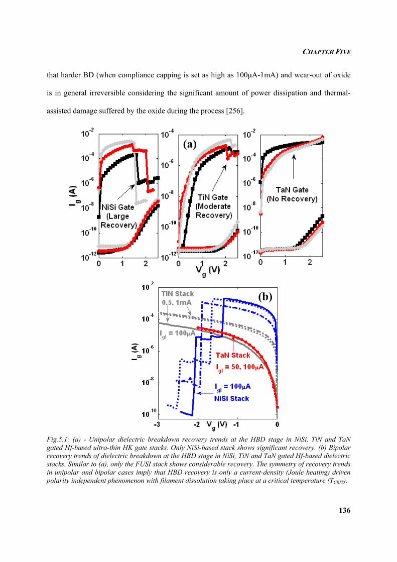
CHAPTER FIVE
136
that harder BD (when compliance capping is set as high as 100µA-1mA) and wear-out of oxide
is in general irreversible considering the significant amount of power dissipation and thermal-
assisted damage suffered by the oxide during the process [256].
Fig.5.1: (a) - Unipolar dielectric breakdown recovery trends at the HBD stage in NiSi, TiN and TaN gated Hf-based ultra-thin HK gate stacks. Only NiSi-based stack shows significant recovery. (b) Bipolar recovery trends of dielectric breakdown at the HBD stage in NiSi, TiN and TaN gated Hf-based dielectric stacks. Similar to (a), only the FUSI stack shows considerable recovery. The symmetry of recovery trends in unipolar and bipolar cases imply that HBD recovery is only a current-density (Joule heating) driven polarity independent phenomenon with filament dissolution taking place at a critical temperature (TCRIT).
(b)
(a)
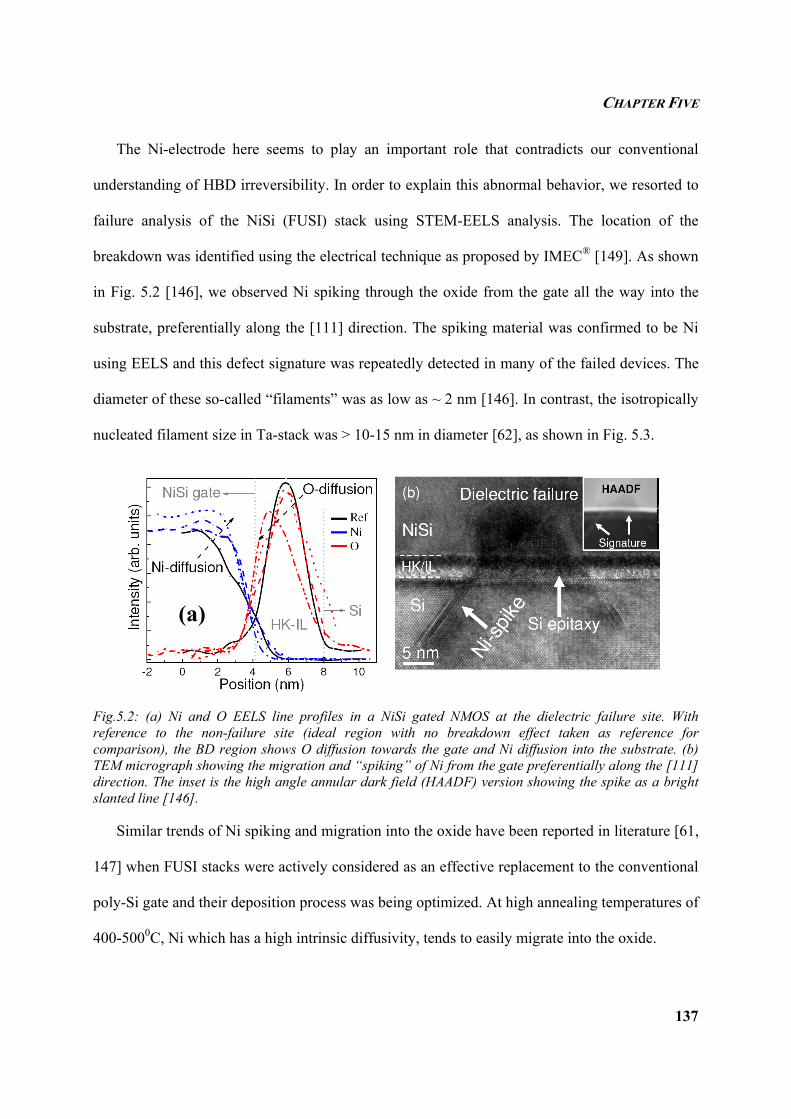
CHAPTER FIVE
137
The Ni-electrode here seems to play an important role that contradicts our conventional
understanding of HBD irreversibility. In order to explain this abnormal behavior, we resorted to
failure analysis of the NiSi (FUSI) stack using STEM-EELS analysis. The location of the
breakdown was identified using the electrical technique as proposed by IMEC® [149]. As shown
in Fig. 5.2 [146], we observed Ni spiking through the oxide from the gate all the way into the
substrate, preferentially along the [111] direction. The spiking material was confirmed to be Ni
using EELS and this defect signature was repeatedly detected in many of the failed devices. The
diameter of these so-called “filaments” was as low as ~ 2 nm [146]. In contrast, the isotropically
nucleated filament size in Ta-stack was > 10-15 nm in diameter [62], as shown in Fig. 5.3.
Fig.5.2: (a) Ni and O EELS line profiles in a NiSi gated NMOS at the dielectric failure site. With reference to the non-failure site (ideal region with no breakdown effect taken as reference for comparison), the BD region shows O diffusion towards the gate and Ni diffusion into the substrate. (b) TEM micrograph showing the migration and “spiking” of Ni from the gate preferentially along the [111] direction. The inset is the high angle annular dark field (HAADF) version showing the spike as a bright slanted line [146].
Similar trends of Ni spiking and migration into the oxide have been reported in literature [61,
147] when FUSI stacks were actively considered as an effective replacement to the conventional
poly-Si gate and their deposition process was being optimized. At high annealing temperatures of
400-5000C, Ni which has a high intrinsic diffusivity, tends to easily migrate into the oxide.
(a)
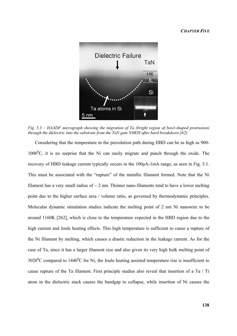
CHAPTER FIVE
138
Fig. 5.3 – HAADF micrograph showing the migration of Ta (bright region of bowl-shaped protrusion) through the dielectric into the substrate from the TaN gate NMOS after hard breakdown [62].
Considering that the temperature in the percolation path during HBD can be as high as 900-
10000C, it is no surprise that the Ni can easily migrate and punch through the oxide. The
recovery of HBD leakage current typically occurs in the 100µA-1mA range, as seen in Fig. 5.1.
This must be associated with the “rupture” of the metallic filament formed. Note that the Ni
filament has a very small radius of ~ 2 nm. Thinner nano-filaments tend to have a lower melting
point due to the higher surface area / volume ratio, as governed by thermodynamic principles.
Molecular dynamic simulation studies indicate the melting point of 2 nm Ni nanowire to be
around 1160K [262], which is close to the temperature expected in the HBD region due to the
high current and Joule heating effects. This high temperature is sufficient to cause a rupture of
the Ni filament by melting, which causes a drastic reduction in the leakage current. As for the
case of Ta, since it has a larger filament size and also given its very high bulk melting point of
30200C compared to 14400C for Ni, the Joule heating assisted temperature rise is insufficient to
cause rupture of the Ta filament. First principle studies also reveal that insertion of a Ta / Ti
atom in the dielectric stack causes the bandgap to collapse, while insertion of Ni causes the
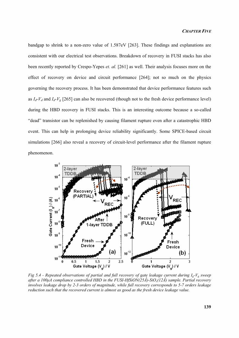
CHAPTER FIVE
139
bandgap to shrink to a non-zero value of 1.587eV [263]. These findings and explanations are
consistent with our electrical test observations. Breakdown of recovery in FUSI stacks has also
been recently reported by Crespo-Yepes et. al. [261] as well. Their analysis focuses more on the
effect of recovery on device and circuit performance [264]; not so much on the physics
governing the recovery process. It has been demonstrated that device performance features such
as Id-Vd and Id-Vg [265] can also be recovered (though not to the fresh device performance level)
during the HBD recovery in FUSI stacks. This is an interesting outcome because a so-called
“dead” transistor can be replenished by causing filament rupture even after a catastrophic HBD
event. This can help in prolonging device reliability significantly. Some SPICE-based circuit
simulations [266] also reveal a recovery of circuit-level performance after the filament rupture
phenomenon.
Fig 5.4 - Repeated observations of partial and full recovery of gate leakage current during Ig-Vg sweep after a 100µA compliance controlled HBD in the FUSI-HfSiON(25Ǻ)-SiOx(12Ǻ) sample. Partial recovery involves leakage drop by 2-3 orders of magnitude, while full recovery corresponds to 5-7 orders leakage reduction such that the recovered current is almost as good as the fresh device leakage value.
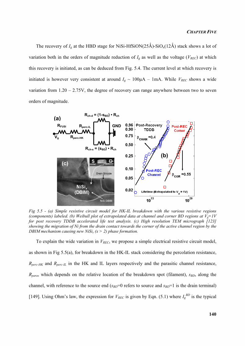
CHAPTER FIVE
140
The recovery of Ig at the HBD stage for NiSi-HfSiON(25Ǻ)-SiOx(12Ǻ) stack shows a lot of
variation both in the orders of magnitude reduction of Ig as well as the voltage (VREC) at which
this recovery is initiated, as can be deduced from Fig. 5.4. The current level at which recovery is
initiated is however very consistent at around Ig ~ 100µA – 1mA. While VREC shows a wide
variation from 1.20 – 2.75V, the degree of recovery can range anywhere between two to seven
orders of magnitude.
Fig 5.5 - (a) Simple resistive circuit model for HK-IL breakdown with the various resistive regions (components) labeled. (b) Weibull plot of extrapolated data at channel and corner BD regions at Vg=1V for post recovery TDDB accelerated life test analysis. (c) High resolution TEM micrograph [123] showing the migration of Ni from the drain contact towards the corner of the active channel region by the DBIM mechanism causing new NiSix (x > 2) phase formation.
To explain the wide variation in VREC, we propose a simple electrical resistive circuit model,
as shown in Fig 5.5(a), for breakdown in the HK-IL stack considering the percolation resistance,
Rperc-HK and Rperc-IL in the HK and IL layers respectively and the parasitic channel resistance,
Rpara, which depends on the relative location of the breakdown spot (filament), sBD, along the
channel, with reference to the source end (sBD=0 refers to source and sBD=1 is the drain terminal)
[149]. Using Ohm’s law, the expression for VREC is given by Eqn. (5.1) where IgBD is the typical
RFUSI Rperc-IL
Rch-d = (1-sBD) • Rch
Rch-s = (sBD) • Rch
Vg
GND
Rperc-HK
(a)
(b)
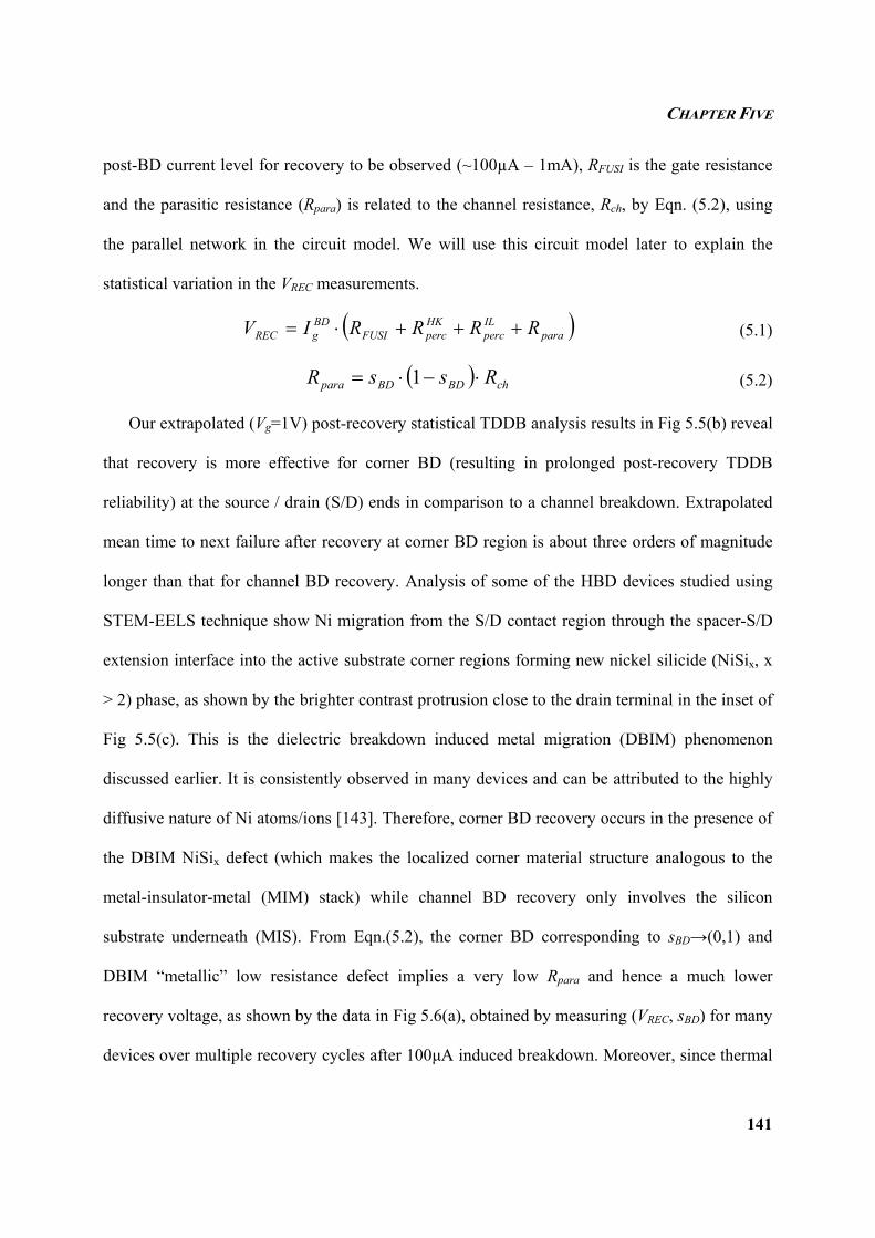
CHAPTER FIVE
141
post-BD current level for recovery to be observed (~100µA – 1mA), RFUSI is the gate resistance
and the parasitic resistance (Rpara) is related to the channel resistance, Rch, by Eqn. (5.2), using
the parallel network in the circuit model. We will use this circuit model later to explain the
statistical variation in the VREC measurements.
( )paraILperc
HKpercFUSI
BDgREC RRRRIV +++⋅= (5.1)
( ) chBDBDpara RssR ⋅−⋅= 1 (5.2)
Our extrapolated (Vg=1V) post-recovery statistical TDDB analysis results in Fig 5.5(b) reveal
that recovery is more effective for corner BD (resulting in prolonged post-recovery TDDB
reliability) at the source / drain (S/D) ends in comparison to a channel breakdown. Extrapolated
mean time to next failure after recovery at corner BD region is about three orders of magnitude
longer than that for channel BD recovery. Analysis of some of the HBD devices studied using
STEM-EELS technique show Ni migration from the S/D contact region through the spacer-S/D
extension interface into the active substrate corner regions forming new nickel silicide (NiSix, x
> 2) phase, as shown by the brighter contrast protrusion close to the drain terminal in the inset of
Fig 5.5(c). This is the dielectric breakdown induced metal migration (DBIM) phenomenon
discussed earlier. It is consistently observed in many devices and can be attributed to the highly
diffusive nature of Ni atoms/ions [143]. Therefore, corner BD recovery occurs in the presence of
the DBIM NiSix defect (which makes the localized corner material structure analogous to the
metal-insulator-metal (MIM) stack) while channel BD recovery only involves the silicon
substrate underneath (MIS). From Eqn.(5.2), the corner BD corresponding to sBD→(0,1) and
DBIM “metallic” low resistance defect implies a very low Rpara and hence a much lower
recovery voltage, as shown by the data in Fig 5.6(a), obtained by measuring (VREC, sBD) for many
devices over multiple recovery cycles after 100µA induced breakdown. Moreover, since thermal
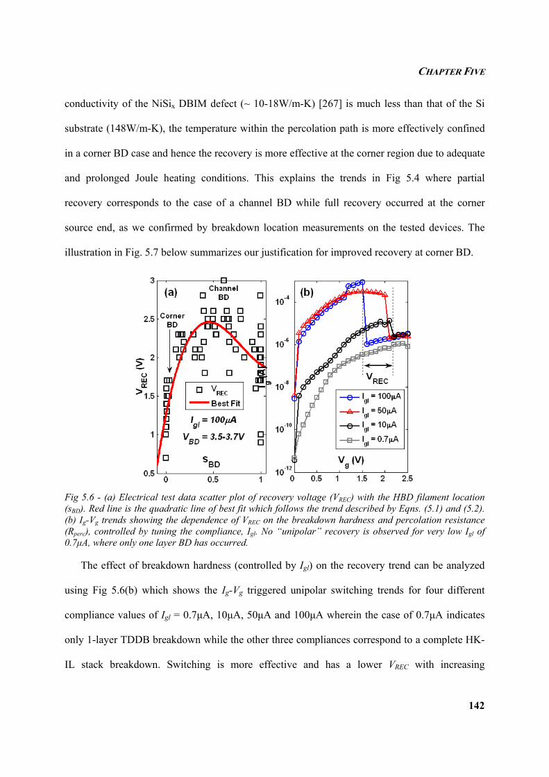
CHAPTER FIVE
142
conductivity of the NiSix DBIM defect (~ 10-18W/m-K) [267] is much less than that of the Si
substrate (148W/m-K), the temperature within the percolation path is more effectively confined
in a corner BD case and hence the recovery is more effective at the corner region due to adequate
and prolonged Joule heating conditions. This explains the trends in Fig 5.4 where partial
recovery corresponds to the case of a channel BD while full recovery occurred at the corner
source end, as we confirmed by breakdown location measurements on the tested devices. The
illustration in Fig. 5.7 below summarizes our justification for improved recovery at corner BD.
Fig 5.6 - (a) Electrical test data scatter plot of recovery voltage (VREC) with the HBD filament location (sBD). Red line is the quadratic line of best fit which follows the trend described by Eqns. (5.1) and (5.2). (b) Ig-Vg trends showing the dependence of VREC on the breakdown hardness and percolation resistance (Rperc), controlled by tuning the compliance, Igl. No “unipolar” recovery is observed for very low Igl of 0.7µA, where only one layer BD has occurred.
The effect of breakdown hardness (controlled by Igl) on the recovery trend can be analyzed
using Fig 5.6(b) which shows the Ig-Vg triggered unipolar switching trends for four different
compliance values of Igl = 0.7µA, 10µA, 50µA and 100µA wherein the case of 0.7µA indicates
only 1-layer TDDB breakdown while the other three compliances correspond to a complete HK-
IL stack breakdown. Switching is more effective and has a lower VREC with increasing
CHAPTER FIVE
143
breakdown hardness, as expected. Therefore, percolation resistance plays a very important role
in controlling VREC as does the parasitic channel resistance.
Fig 5.7 – Illustrating the SET (a, c) and RESET (b, d) transitions for a single HBD filament at channel (a, b) and corner (c, d) regions. Better switching is expected for corner filaments due to low resistivity NiSix phase formation at the S/D extension region that induces an MIM-like stack and enhances the thermal confinement.
For a single layer IL BD case, Rperc-IL << Rperc-HK and Rperc-HK ~ 1-10MΩ which is the typical
percolation resistance for a functional dielectric [268]. For percolation resistance in the MΩ
range, from Eqn. (5.1), VREC ~ 1000V obviously suggesting that it is impossible to achieve
recovery after a single-layer TDDB. However, when the complete stack breaks down at Igl >
5µA, Rperc-HK ~ Rperc-IL and (Rperc-HK + Rperc-IL) ~ 1-10kΩ. In the low kΩ range, VREC is close to 1V
and since in this case VREC < VBD (found to be 3.5 - 3.7V), it is practically possible to achieve
breakdown reversibility. Since circuit level failures at operating conditions can occur only by
multiple IL SBD events, recovery of the HBD event may not be critical and useful from a
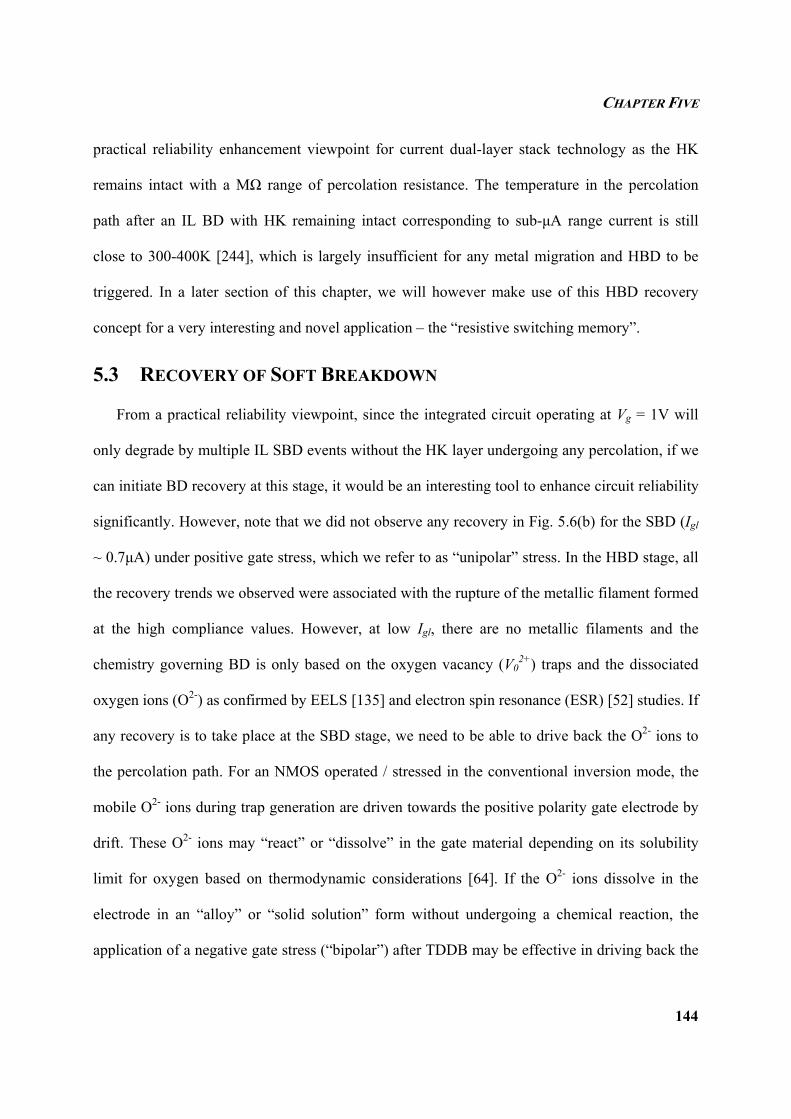
CHAPTER FIVE
144
practical reliability enhancement viewpoint for current dual-layer stack technology as the HK
remains intact with a MΩ range of percolation resistance. The temperature in the percolation
path after an IL BD with HK remaining intact corresponding to sub-µA range current is still
close to 300-400K [244], which is largely insufficient for any metal migration and HBD to be
triggered. In a later section of this chapter, we will however make use of this HBD recovery
concept for a very interesting and novel application – the “resistive switching memory”.
5.3 RECOVERY OF SOFT BREAKDOWN
From a practical reliability viewpoint, since the integrated circuit operating at Vg = 1V will
only degrade by multiple IL SBD events without the HK layer undergoing any percolation, if we
can initiate BD recovery at this stage, it would be an interesting tool to enhance circuit reliability
significantly. However, note that we did not observe any recovery in Fig. 5.6(b) for the SBD (Igl
~ 0.7µA) under positive gate stress, which we refer to as “unipolar” stress. In the HBD stage, all
the recovery trends we observed were associated with the rupture of the metallic filament formed
at the high compliance values. However, at low Igl, there are no metallic filaments and the
chemistry governing BD is only based on the oxygen vacancy (V02+) traps and the dissociated
oxygen ions (O2-) as confirmed by EELS [135] and electron spin resonance (ESR) [52] studies. If
any recovery is to take place at the SBD stage, we need to be able to drive back the O2- ions to
the percolation path. For an NMOS operated / stressed in the conventional inversion mode, the
mobile O2- ions during trap generation are driven towards the positive polarity gate electrode by
drift. These O2- ions may “react” or “dissolve” in the gate material depending on its solubility
limit for oxygen based on thermodynamic considerations [64]. If the O2- ions dissolve in the
electrode in an “alloy” or “solid solution” form without undergoing a chemical reaction, the
application of a negative gate stress (“bipolar”) after TDDB may be effective in driving back the
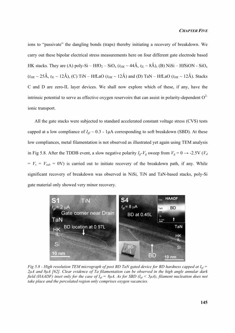
CHAPTER FIVE
145
ions to “passivate” the dangling bonds (traps) thereby initiating a recovery of breakdown. We
carry out these bipolar electrical stress measurements here on four different gate electrode based
HK stacks. They are (A) poly-Si – HfO2 – SiOx (tHK ~ 44Ǻ, tIL ~ 8Ǻ), (B) NiSi – HfSiON - SiOx
(tHK ~ 25Ǻ, tIL ~ 12Ǻ), (C) TiN – HfLaO (tHK ~ 12Ǻ) and (D) TaN – HfLaO (tHK ~ 12Ǻ). Stacks
C and D are zero-IL layer devices. We shall now explore which of these, if any, have the
intrinsic potential to serve as effective oxygen reservoirs that can assist in polarity-dependent O2-
ionic transport.
All the gate stacks were subjected to standard accelerated constant voltage stress (CVS) tests
capped at a low compliance of Igl ~ 0.3 - 1µA corresponding to soft breakdown (SBD). At these
low compliances, metal filamentation is not observed as illustrated yet again using TEM analysis
in Fig 5.8. After the TDDB event, a slow negative polarity Ig-Vg sweep from Vg = 0 → -2.5V (Vd
= Vs = Vsub = 0V) is carried out to initiate recovery of the breakdown path, if any. While
significant recovery of breakdown was observed in NiSi, TiN and TaN-based stacks, poly-Si
gate material only showed very minor recovery.
Fig 5.8 - High resolution TEM micrograph of post BD TaN gated device for BD hardness capped at Igl = 2µA and 8µA [62]. Clear evidence of Ta filamentation can be observed in the high angle annular dark field (HAADF) inset only for the case of Igl = 8µA. As for SBD (Igl < 5µA), filament nucleation does not take place and the percolated region only comprises oxygen vacancies.
CHAPTER FIVE
146
Fig 5.9 - Ig-Vg plots for (a) poly-Si (0.25µm2), (b) NiSi (0.12µm2), (c) TiN (90nm × 100nm) and (d) TaN (90nm × 100nm) gated Hf-based dielectric stacks for SBD with different compliance settings corresponding to a wide range of BD hardness. The solid lines correspond to the case of SBD, while the dotted lines represent the leakage conduction measured after negative Ig-Vg sweep induced recovery (see Fig 5.10(a)). The dash-dotted grey line is the initial leakage current prior to stress testing.
Fig 5.9 shows the post-recovery trends in Ig-Vg for (a) poly-Si, (b) NiSi, (c) TiN and (d) TaN
gate materials for the case of SBD with different compliance capping (Igl ~ 0.2 - 4µA),
corresponding to a range of pre-filament BD hardness. The reduction in leakage current (dotted
lines) in Fig. 5.9, after a negative sweep induced recovery (shown in Fig. 5.10(a)) can be clearly
seen for all the gate stacks implying the possibility of O2- ion drift back to passivate the
percolation path during the opposite polarity voltage sweep [269]. The trends also reveal that
recovery is very minor for poly-Si gated stacks while moderate recovery is seen in NiSi and TaN
stacks. As for the TiN gate stack, excellent recovery with post-recovery gate current (IREC) being
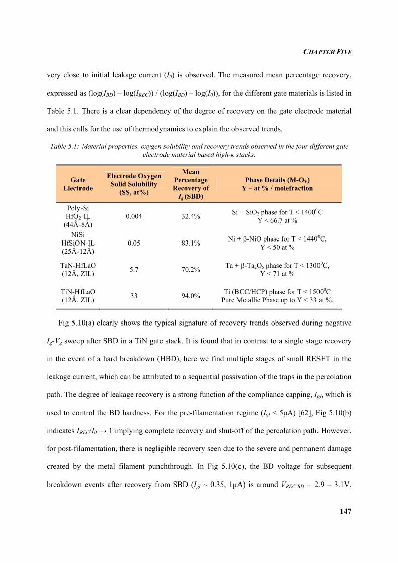
CHAPTER FIVE
147
very close to initial leakage current (I0) is observed. The measured mean percentage recovery,
expressed as (log(IBD) – log(IREC)) / (log(IBD) – log(I0)), for the different gate materials is listed in
Table 5.1. There is a clear dependency of the degree of recovery on the gate electrode material
and this calls for the use of thermodynamics to explain the observed trends.
Table 5.1: Material properties, oxygen solubility and recovery trends observed in the four different gate electrode material based high-κ stacks.
Gate Electrode
Electrode Oxygen Solid Solubility
(SS, at%)
Mean Percentage Recovery of
Ig (SBD)
Phase Details (M-OY) Y – at % / molefraction
Poly-Si HfO2-IL
(44Ǻ-8Ǻ) 0.004 32.4% Si + SiO2 phase for T < 14000C
Y < 66.7 at %
NiSi HfSiON-IL (25Ǻ-12Ǻ)
0.05 83.1% Ni + β-NiO phase for T < 14400C, Y < 50 at %
TaN-HfLaO (12Ǻ, ZIL) 5.7 70.2% Ta + β-Ta2O5 phase for T < 13000C,
Y < 71 at %
TiN-HfLaO (12Ǻ, ZIL) 33 94.0% Ti (BCC/HCP) phase for T < 15000C
Pure Metallic Phase up to Y < 33 at %.
Fig 5.10(a) clearly shows the typical signature of recovery trends observed during negative
Ig-Vg sweep after SBD in a TiN gate stack. It is found that in contrast to a single stage recovery
in the event of a hard breakdown (HBD), here we find multiple stages of small RESET in the
leakage current, which can be attributed to a sequential passivation of the traps in the percolation
path. The degree of leakage recovery is a strong function of the compliance capping, Igl, which is
used to control the BD hardness. For the pre-filamentation regime (Igl < 5µA) [62], Fig 5.10(b)
indicates IREC/I0 → 1 implying complete recovery and shut-off of the percolation path. However,
for post-filamentation, there is negligible recovery seen due to the severe and permanent damage
created by the metal filament punchthrough. In Fig 5.10(c), the BD voltage for subsequent
breakdown events after recovery from SBD (Igl ~ 0.35, 1µA) is around VREC-BD = 2.9 – 3.1V,
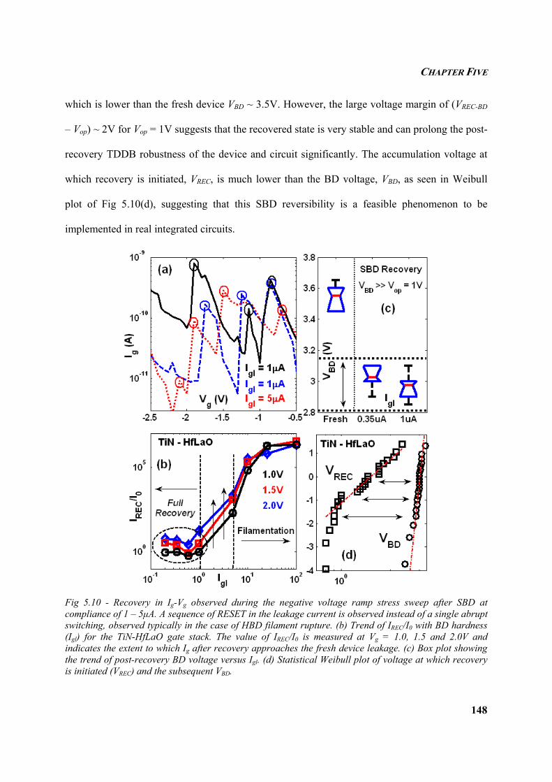
CHAPTER FIVE
148
which is lower than the fresh device VBD ~ 3.5V. However, the large voltage margin of (VREC-BD
– Vop) ~ 2V for Vop = 1V suggests that the recovered state is very stable and can prolong the post-
recovery TDDB robustness of the device and circuit significantly. The accumulation voltage at
which recovery is initiated, VREC, is much lower than the BD voltage, VBD, as seen in Weibull
plot of Fig 5.10(d), suggesting that this SBD reversibility is a feasible phenomenon to be
implemented in real integrated circuits.
Fig 5.10 - Recovery in Ig-Vg observed during the negative voltage ramp stress sweep after SBD at compliance of 1 – 5µA. A sequence of RESET in the leakage current is observed instead of a single abrupt switching, observed typically in the case of HBD filament rupture. (b) Trend of IREC/I0 with BD hardness (Igl) for the TiN-HfLaO gate stack. The value of IREC/I0 is measured at Vg = 1.0, 1.5 and 2.0V and indicates the extent to which Ig after recovery approaches the fresh device leakage. (c) Box plot showing the trend of post-recovery BD voltage versus Igl. (d) Statistical Weibull plot of voltage at which recovery is initiated (VREC) and the subsequent VBD.
CHAPTER FIVE
149
The material-dependent SBD reversibility phenomena can be attributed to the oxygen
gettering property and high oxygen solubility in Ti, Ta and Ni -gated stacks. The gettering
property of Ti-based MG has previously been used as an effective technique to scavenge the
interfacial layer (IL) [65, 66]. Table 5.1 provides details of the terminal solid solubility (SS) of
oxygen and phase formation in Ni-O, Ti-O and Ta-O systems [270-272]. The high value of SS in
Ti and Ta gate stack and co-existence of binary Ni-NiO (β-phase) for large atomic percent of O
imply that all the three metals function as good oxygen reservoirs. The mobile O2- ions generated
from bond breaking during stress induced leakage current trap generation drift to the metal gate
and exist as a M(metal)-O solid solution (alloy). The metal gate does not get oxidized for low O-
activity. Application of a negative bias can push back the O2- ions to passivate the V02+ traps (by
forming back Hf-O / Si-O bonds to lower system free energy) that constitute the percolation
path, thereby shutting it off. Another source of O2- ions stored in the metal gate is through the
reduction of the IL (M + SiOx → M-Ox + Si) which causes O2- ions from IL to permeate through
the HK into the M-gate. The small recovery of 32.4% in poly-Si gate stacks is due to the very
low oxygen SS of 0.004% in Si. Another factor that could influence the recovery phenomenon is
the oxygen affinity, referring to the Gibbs free energy of formation of the metal gate oxides.
Since Ni has a very low oxygen affinity, it is unfeasible to oxidize it easily and hence it shows
very good recovery. The same argument holds true for TiN and TaN. Poly-Si however has high
affinity for oxygen and hence the O2- ions entering the gate material tend to oxidize the Si to
form Si-O bonds.
It is also necessary to consider the impact, if any, of the dielectric material, its thickness,
microstructure and doping on the SBD recovery. Since, passivation of traps occurs by “drift” of
O2- ions, we expect a low sensitivity to oxide thickness (as long as the oxide is not too thick to
CHAPTER FIVE
150
suffer from destructive damage during percolation). The presence of grain boundaries (GB) in
polycrystalline high-κ stacks can serve as fast diffusion paths for oxygen, thereby assisting in the
recovery process in the event of an IL SBD, adjacent to the GB [273]. However, since the
defective GB region serves as a sink for oxygen vacancies [74], very low post-recovery leakage
states may not be achievable. We therefore expect amorphous HK materials to show better
window of recovery. The improved recovery in the NiSi samples we observed, could be
attributed to the amorphous nature of HfSiON. We postulate that the La-doping of HfO2 in the
TiN and TaN-based stacks we have tested, also plays a role in ensuring better recovery because
La has a very high oxygen affinity compared to Hf or Si [274], and therefore, La-O bonding (and
V02+ passivation) is thermodynamically feasible.
It is known at circuit level (large area) and we have also proven the same that, for Vop ~ 1V,
multiple SBD events occur as opposed to a single HBD event [171]. The driving force for
filamentation failure is insufficient at Vg = Vop. As many as 15000 BD spots can form in a circuit
with area 0.01 cm2 at Vop ~ 1V [171]. The SBD reversibility we have observed can be used to
very effectively repair most of these BD spots, thereby replenishing circuit performance and
prolonging its TDDB lifetime. We may also use this to reduce stress induced leakage currents
prior to the TDDB event.
In summary, an interesting phenomenon of SBD reversibility in Ti, Ta and Ni-based MG-HK
stacks has been presented. Varying degree of recovery was observed across different gate stack
technologies. The results here can be used as a design for reliability (DFR) initiative to choose
MG materials with high oxygen solubility that can function as effective oxygen reservoirs and
passivate percolated traps during multiple SBD events at circuit level by initiating a simple on-
CHAPTER FIVE
151
chip “reflash” (application of negative voltage) that can be programmed at pre-determined
intervals thereby bringing in the novel concept of “self-repair” of an integrated circuit.
5.4 CORRELATING BREAKDOWN RECOVERY TO SWITCHING
So far, all our analysis above dealt with the observation of dielectric breakdown “recovery”
in the SBD and HBD stages of MG-HK stacks. While only “bipolar” mode of recovery is
possible for SBD confined to oxygen gettering Ti, Ta and Ni-based gate electrodes, both
“unipolar” and “bipolar” modes of recovery are observed in HBD, but restricted only to the low
melting point spiking Ni electrode. Our main aim in the previous sections was to investigate
whether the TDDB robustness and lifetime of MG-HK stacks could be prolonged by these
means. It is worth noting that this repeated multi-cycle breakdown and recovery phenomenon
can be looked at from a completely different perspective of “switching” between two states – the
high resistance state (HRS) and low resistance state (LRS). The concept of resistance switching
is an important area of study as it finds direct application in non-volatile memory (NVM)
technologies in the near future. Currently the NVM used for data storage in nanoelectronic
applications consists of different variants of the charge trap-based Flash memory (resembling
and compatible to CMOS logic technology) which consists of a tunnel oxide, charge trap layer
and a control dielectric. Though Flash devices have served as a good structure for NVM
applications over the past decade, with aggressive scaling, issues such as random telegraph noise
(RTN), SILC through the tunneling dielectric and charge de-trapping from the tunnel oxide have
increased the performance variability and reduced the retention reliability of this memory
technology significantly [275]. Achieving multi-bit storage applications has become increasingly
difficult considering the shrinking threshold voltage (VT) windows between distinct bit levels.
Moreover, we are approaching the regime of “few electron effects” [275], wherein the number of
CHAPTER FIVE
152
stored electrons for a 32 nm node is only about 100. Therefore, the stochastic process of carrier
tunneling induces significant variability. Other disadvantages of the Flash memory include the
need for high voltage to program / erase (P/E) and relatively low endurance (~ 105 cycles).
Considering the limitations of Flash memory technology and its variants for further
downscaling, resistive random access memory (RRAM) has been proposed to be the most suited
replacement for future NVM devices. The RRAM (also referred to as “memristor” – voltage
controlled resistor) is a simple metal-insulator-metal (MIM) capacitor which operates based on
the principle of repeated reversible transitions between HRS and LRS by application of different
range and/or polarity of voltages to the top (TE) / bottom electrode (BE). The TE and BE are
analogous to the gate and substrate terminals we refer to in logic devices. Though the concept of
“resistive switching” and conductivity transition has been around for the past 4-5 decades [276,
277], its application to RRAM in the form of memristors was only recently realized by Hewlett
Packard® (HP) [151] in 2008. This has generated renewed interest in RRAM over the past few
years, considering its potential to replace Flash as a more robust NVM technology for the future.
Some of the advantages of RRAM include its simple MIM structure, CMOS compatible
material and process flow, easy design and fabrication, multi-bit storage realization, aggressive
scalability, high integration density, prolonged endurance and enhanced switching speed in the
nanosecond range [48]. There are many mechanisms proposed and speculated to explain the
voltage-controlled resistance switching in RRAM which include oxygen ion / oxygen vacancy
transport [154, 155], metal filament nucleation and rupture [156], electrochemical redox
reactions [157] and electron trapping / detrapping [158]. However, there is limited evidence in
strong support of any of these mechanisms and it is also evident that the fundamental mechanism
is very much dependent on the material used for the electrode and the dielectric.
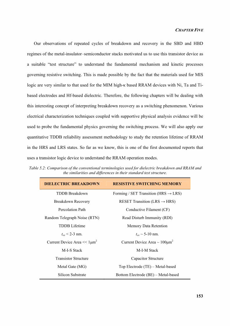
CHAPTER FIVE
153
Our observations of repeated cycles of breakdown and recovery in the SBD and HBD
regimes of the metal-insulator–semiconductor stacks motivated us to use this transistor device as
a suitable “test structure” to understand the fundamental mechanism and kinetic processes
governing resistive switching. This is made possible by the fact that the materials used for MIS
logic are very similar to that used for the MIM high-κ based RRAM devices with Ni, Ta and Ti-
based electrodes and Hf-based dielectric. Therefore, the following chapters will be dealing with
this interesting concept of interpreting breakdown recovery as a switching phenomenon. Various
electrical characterization techniques coupled with supportive physical analysis evidence will be
used to probe the fundamental physics governing the switching process. We will also apply our
quantitative TDDB reliability assessment methodology to study the retention lifetime of RRAM
in the HRS and LRS states. So far as we know, this is one of the first documented reports that
uses a transistor logic device to understand the RRAM operation modes.
Table 5.2: Comparison of the conventional terminologies used for dielectric breakdown and RRAM and the similarities and differences in their standard test structure.
DIELECTRIC BREAKDOWN RESISTIVE SWITCHING MEMORY
TDDB Breakdown Forming / SET Transition (HRS → LRS)
Breakdown Recovery RESET Transition (LRS → HRS)
Percolation Path Conductive Filament (CF)
Random Telegraph Noise (RTN) Read Disturb Immunity (RDI)
TDDB Lifetime Memory Data Retention
tox < 2-3 nm. tox ~ 5-10 nm.
Current Device Area << 1µm2 Current Device Area ~ 100µm2
M-I-S Stack M-I-M Stack
Transistor Structure Capacitor Structure
Metal Gate (MG) Top Electrode (TE) – Metal-based
Silicon Substrate Bottom Electrode (BE) – Metal-based
CHAPTER FIVE
154
The similarities and differences between the M-I-S logic and M-I-M memory are listed in
Table 5.2 along with the different terminologies used to represent the same (similar) phenomena.
It is these analogies between the two devices that inspired us to use the breakdown recovery as a
tool to understand the switching mechanism. There are various advantages of using our M-I-S
stacks for switching study :–
The conductive filament (CF) location / BD spot (sBD) during every switching cycle can be
easily located along the length of the transistor channel using simple electrical measurements and
calculation of the weighted ratio of Id and Is : sBD = Id / (Id + Is) → this will help us identify
whether the filamentation process is random or localized.
The M-I-S stack being asymmetric with an oxygen gettering ‘M’ and poor oxygen soluble
material ‘S’ helps us decipher the movement of the oxygen ions and their exact role in the
switching process – such analysis is more tricky for an M-I-M stack.
Our stack fabricated using the optimized CMOS process has very smooth metal-oxide and
oxide-substrate interfaces as opposed to current RRAM reports where the interfaces seem to be
very rough due to unoptimized process design – the presence of an atomically smooth interface
and good quality oxide in our devices helps focus on the intrinsic switching nature of RRAM and
also assess its performance variability when implemented for future memory technology nodes.
The device area we use for all tests is ~ 0.10-0.50 µm2 as opposed to the large RRAM
capacitor areas > 100 µm2 [278]. When RRAM is commercialized, it is likely to be implemented
with a very small area of 10 nm × 10 nm [279, 280]. Therefore, studying switching in small area
devices is a critical requirement so that the impact of area scaling on switching characteristics
can be gauged.
CHAPTER FIVE
155
The dielectric thickness in our MIS stack is ~ 2-3 nm as opposed to the very thick oxides of
5-10 nm [281] (sometimes even 20-50 nm [282]) that are currently under investigation. Again,
the impact of downscaling will require ultra-thin dielectric based RRAM in the near future,
which our current logic stack can help us to study.
Lastly, it is hard to perform in-depth physical analysis on large area RRAM as there are no
electrical means to detect the location of the CF. Except for very fortunate circumstances,
focusing on the right area to carry out in-depth physical and chemical imaging is an arduous and
ineffective task. This problem is overcome in our gate stack as we can identify the CF location
along the channel length and scan across the width of our “small area” structure to be able to nail
down the filament geography with a higher success rate.
5.5 SUMMARY
In this chapter, we presented an interesting finding on recovery of dielectric breakdown in
the SBD and HBD regimes. This recovery is found to be highly gate electrode dependent and is
governed by the oxygen solid solubility and melting point of the electrode for SBD and HBD
respectively. While SBD recovery was highly polarity-dependent, HBD recovery is non-polar.
We have also discussed the correlation of this recovery process to the resistive switching
phenomenon and justified the use of our MIS transistor as a test structure for improved
understanding of the fundamentals governing the switching mechanism.
In the following chapter, we will use a suite of electrical characterization tools and oxygen
gettering electrode stacks to probe this switching mechanism in detail and analyze its
dependence on the compliance capping for the forming / SET transitions.
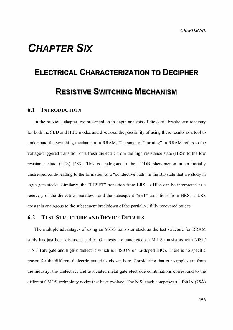
CHAPTER SIX
156
CHAPTER SIX
EEELLLEEECCCTTTRRRIIICCCAAALLL CCCHHHAAARRRAAACCCTTTEEERRRIIIZZZAAATTTIIIOOONNN TTTOOO DDDEEECCCIIIPPPHHHEEERRR
RRREEESSSIIISSSTTTIIIVVVEEE SSSWWWIIITTTCCCHHHIIINNNGGG MMMEEECCCHHHAAANNNIIISSSMMM
6.1 INTRODUCTION
In the previous chapter, we presented an in-depth analysis of dielectric breakdown recovery
for both the SBD and HBD modes and discussed the possibility of using these results as a tool to
understand the switching mechanism in RRAM. The stage of “forming” in RRAM refers to the
voltage-triggered transition of a fresh dielectric from the high resistance state (HRS) to the low
resistance state (LRS) [283]. This is analogous to the TDDB phenomenon in an initially
unstressed oxide leading to the formation of a “conductive path” in the BD state that we study in
logic gate stacks. Similarly, the “RESET” transition from LRS → HRS can be interpreted as a
recovery of the dielectric breakdown and the subsequent “SET” transitions from HRS → LRS
are again analogous to the subsequent breakdown of the partially / fully recovered oxides.
6.2 TEST STRUCTURE AND DEVICE DETAILS
The multiple advantages of using an M-I-S transistor stack as the test structure for RRAM
study has just been discussed earlier. Our tests are conducted on M-I-S transistors with NiSi /
TiN / TaN gate and high-κ dielectric which is HfSiON or La-doped HfO2. There is no specific
reason for the different dielectric materials chosen here. Considering that our samples are from
the industry, the dielectrics and associated metal gate electrode combinations correspond to the
different CMOS technology nodes that have evolved. The NiSi stack comprises a HfSiON (25Ǻ)
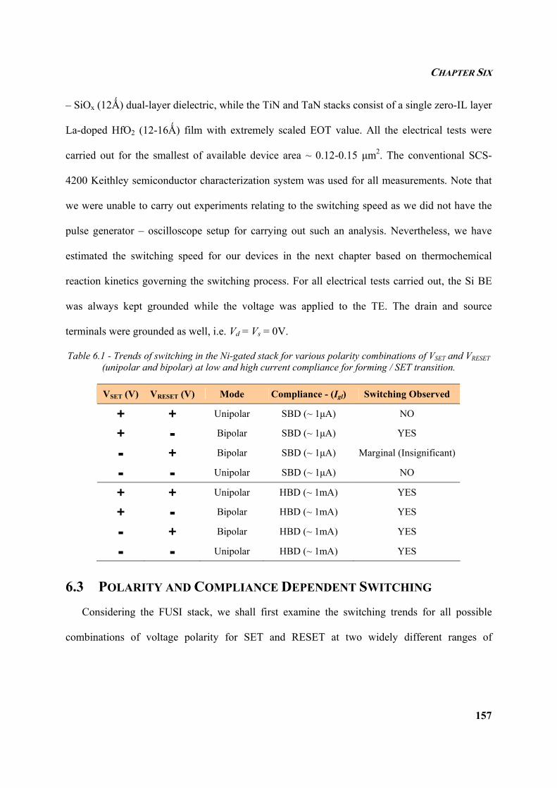
CHAPTER SIX
157
– SiOx (12Ǻ) dual-layer dielectric, while the TiN and TaN stacks consist of a single zero-IL layer
La-doped HfO2 (12-16Ǻ) film with extremely scaled EOT value. All the electrical tests were
carried out for the smallest of available device area ~ 0.12-0.15 µm2. The conventional SCS-
4200 Keithley semiconductor characterization system was used for all measurements. Note that
we were unable to carry out experiments relating to the switching speed as we did not have the
pulse generator – oscilloscope setup for carrying out such an analysis. Nevertheless, we have
estimated the switching speed for our devices in the next chapter based on thermochemical
reaction kinetics governing the switching process. For all electrical tests carried out, the Si BE
was always kept grounded while the voltage was applied to the TE. The drain and source
terminals were grounded as well, i.e. Vd = Vs = 0V.
Table 6.1 - Trends of switching in the Ni-gated stack for various polarity combinations of VSET and VRESET (unipolar and bipolar) at low and high current compliance for forming / SET transition.
VSET (V) VRESET (V) Mode Compliance - (Igl) Switching Observed
+ + Unipolar SBD (~ 1µA) NO
+ - Bipolar SBD (~ 1µA) YES
- + Bipolar SBD (~ 1µA) Marginal (Insignificant)
- - Unipolar SBD (~ 1µA) NO
+ + Unipolar HBD (~ 1mA) YES
+ - Bipolar HBD (~ 1mA) YES
- + Bipolar HBD (~ 1mA) YES
- - Unipolar HBD (~ 1mA) YES
6.3 POLARITY AND COMPLIANCE DEPENDENT SWITCHING
Considering the FUSI stack, we shall first examine the switching trends for all possible
combinations of voltage polarity for SET and RESET at two widely different ranges of
CHAPTER SIX
158
compliance values (Igl ~ 0.3-2µA and Igl ~ 100µA-1mA). There are four possible polarity
combinations of VSET and VRESET, for which the switching trends are summarized in Table 6.1.
Fig 6.1 - Trends of RESET in the oxygen vacancy governed regime (low compliance) for the following cases : (a) and (d) are unipolar modes with positive and negative TE voltage, respectively. (b) and (c) are bipolar modes with VSET > 0V and VSET < 0V, respectively. Significant switching is only observed for bipolar mode in (b) due to the high oxygen solubility of the metal-based TE, while the silicon BE does not function as an oxygen reservoir.
Fig. 6.1 shows the Ig-Vg trends of RESET at low Igl (0.3-2µA) for the four different voltage
polarities : (a) VSET > 0V, VRESET > 0V, (b) VSET > 0V, VRESET < 0V, (c) VSET < 0V, VRESET > 0V
and (d) VSET < 0V, VRESET < 0V. Cases (a) and (d) refer to unipolar mode of operation wherein no
switching is observed at all, while cases (b) and (c) represent the bipolar mode in which, case (c)
shows small kinks with very minimal drop in conductance. In striking contrast, we observed very
significant drop (about 2-3 orders of magnitude) in the current in multiple stages for case (b)
only, indicating a large transition from the low to high resistance state (LRS → HRS). It is clear
CHAPTER SIX
159
that there is no unipolar mode of switching here and the bipolar RESET behavior is highly
asymmetric as well. These differences in the switching trends will help us unearth the switching
mechanism.
As shown in Fig. 6.2(a) from Ref. [146], the TEM micrograph after SET (breakdown) for
low Igl does not show any obvious physical microstructural defect, implying that the conducting
filament is purely consisting of oxygen vacancies (V02+), while the mobile oxygen ions migrate
and drift away. The absence of unipolar mode switching in Fig. 6.1 further confirms our claim
that oxygen ion charged species (O2-) are responsible for SET and RESET at low Igl. Only
opposite polarity of voltages and associated drift forces can cause to-and-fro reversible motion of
the O2- ions.
Fig 6.2 - TEM micrographs of devices after forming stage with compliance capped at (a) Igl = 5µA and (b) Igl = 100µA respectively [146]. It is clear that metal filaments nucleate only for Igl >> 5µA.
The asymmetry in the bipolar switching trend is an interesting result and can be explained by
the differential response of the TE and BE materials to the O2- ions that drift into these films.
While metal electrodes such as NiSi, TiN and TaN can serve as good oxygen reservoirs, Si has
very poor oxygen solubility and high oxygen affinity, i.e. Gibbs free energy of oxidation for Si-O
is very favorable. Therefore, the O2- ions which drift towards the Si BE tend to react with it
10 nm
(b) (a)
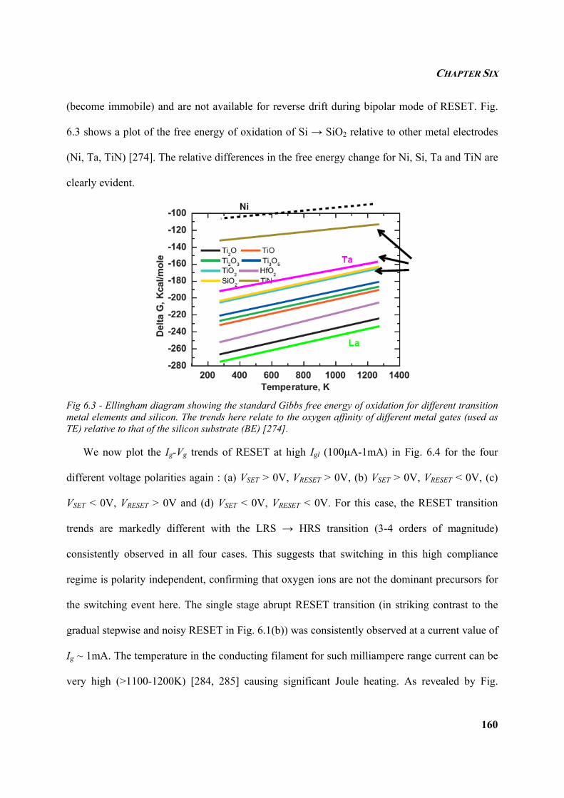
CHAPTER SIX
160
(become immobile) and are not available for reverse drift during bipolar mode of RESET. Fig.
6.3 shows a plot of the free energy of oxidation of Si → SiO2 relative to other metal electrodes
(Ni, Ta, TiN) [274]. The relative differences in the free energy change for Ni, Si, Ta and TiN are
clearly evident.
Fig 6.3 - Ellingham diagram showing the standard Gibbs free energy of oxidation for different transition metal elements and silicon. The trends here relate to the oxygen affinity of different metal gates (used as TE) relative to that of the silicon substrate (BE) [274].
We now plot the Ig-Vg trends of RESET at high Igl (100µA-1mA) in Fig. 6.4 for the four
different voltage polarities again : (a) VSET > 0V, VRESET > 0V, (b) VSET > 0V, VRESET < 0V, (c)
VSET < 0V, VRESET > 0V and (d) VSET < 0V, VRESET < 0V. For this case, the RESET transition
trends are markedly different with the LRS → HRS transition (3-4 orders of magnitude)
consistently observed in all four cases. This suggests that switching in this high compliance
regime is polarity independent, confirming that oxygen ions are not the dominant precursors for
the switching event here. The single stage abrupt RESET transition (in striking contrast to the
gradual stepwise and noisy RESET in Fig. 6.1(b)) was consistently observed at a current value of
Ig ~ 1mA. The temperature in the conducting filament for such milliampere range current can be
very high (>1100-1200K) [284, 285] causing significant Joule heating. As revealed by Fig.
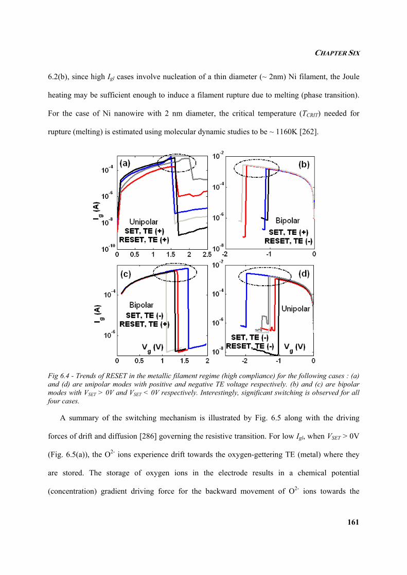
CHAPTER SIX
161
6.2(b), since high Igl cases involve nucleation of a thin diameter (~ 2nm) Ni filament, the Joule
heating may be sufficient enough to induce a filament rupture due to melting (phase transition).
For the case of Ni nanowire with 2 nm diameter, the critical temperature (TCRIT) needed for
rupture (melting) is estimated using molecular dynamic studies to be ~ 1160K [262].
Fig 6.4 - Trends of RESET in the metallic filament regime (high compliance) for the following cases : (a) and (d) are unipolar modes with positive and negative TE voltage respectively. (b) and (c) are bipolar modes with VSET > 0V and VSET < 0V respectively. Interestingly, significant switching is observed for all four cases.
A summary of the switching mechanism is illustrated by Fig. 6.5 along with the driving
forces of drift and diffusion [286] governing the resistive transition. For low Igl, when VSET > 0V
(Fig. 6.5(a)), the O2- ions experience drift towards the oxygen-gettering TE (metal) where they
are stored. The storage of oxygen ions in the electrode results in a chemical potential
(concentration) gradient driving force for the backward movement of O2- ions towards the
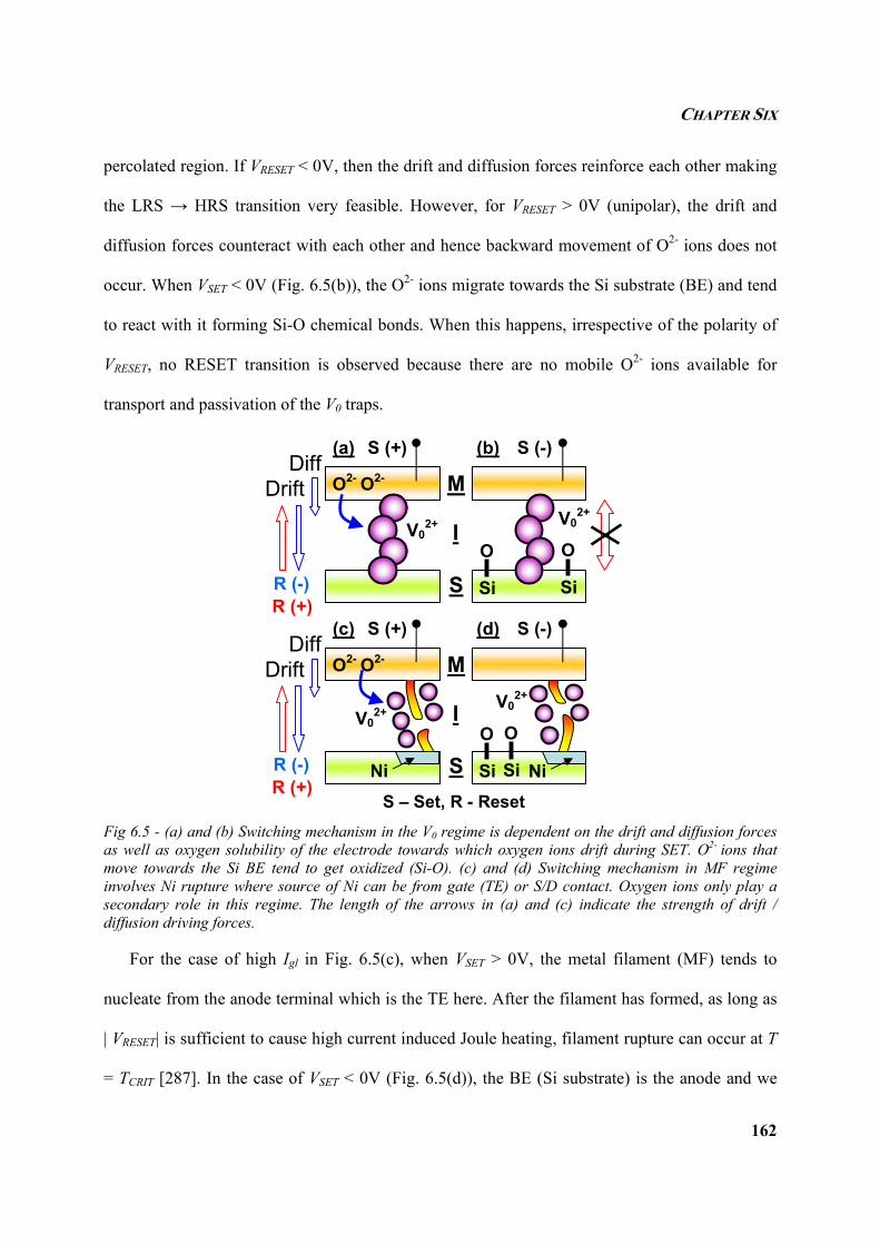
CHAPTER SIX
162
percolated region. If VRESET < 0V, then the drift and diffusion forces reinforce each other making
the LRS → HRS transition very feasible. However, for VRESET > 0V (unipolar), the drift and
diffusion forces counteract with each other and hence backward movement of O2- ions does not
occur. When VSET < 0V (Fig. 6.5(b)), the O2- ions migrate towards the Si substrate (BE) and tend
to react with it forming Si-O chemical bonds. When this happens, irrespective of the polarity of
VRESET, no RESET transition is observed because there are no mobile O2- ions available for
transport and passivation of the V0 traps.
Fig 6.5 - (a) and (b) Switching mechanism in the V0 regime is dependent on the drift and diffusion forces as well as oxygen solubility of the electrode towards which oxygen ions drift during SET. O2- ions that move towards the Si BE tend to get oxidized (Si-O). (c) and (d) Switching mechanism in MF regime involves Ni rupture where source of Ni can be from gate (TE) or S/D contact. Oxygen ions only play a secondary role in this regime. The length of the arrows in (a) and (c) indicate the strength of drift / diffusion driving forces.
For the case of high Igl in Fig. 6.5(c), when VSET > 0V, the metal filament (MF) tends to
nucleate from the anode terminal which is the TE here. After the filament has formed, as long as
| VRESET| is sufficient to cause high current induced Joule heating, filament rupture can occur at T
= TCRIT [287]. In the case of VSET < 0V (Fig. 6.5(d)), the BE (Si substrate) is the anode and we
O2- O2-
V02+
S (+)
O
(a) S (-) Diff
Drift
R (-) R (+)
V02+
M
I
S Si
O
Si
(b)
O2- O2-
V02+
S (+)
(c) S (-)
V02+
M
I
S
(d)
Ni Ni
Diff Drift
R (-) R (+)
O
Si
O
Si
S – Set, R - Reset
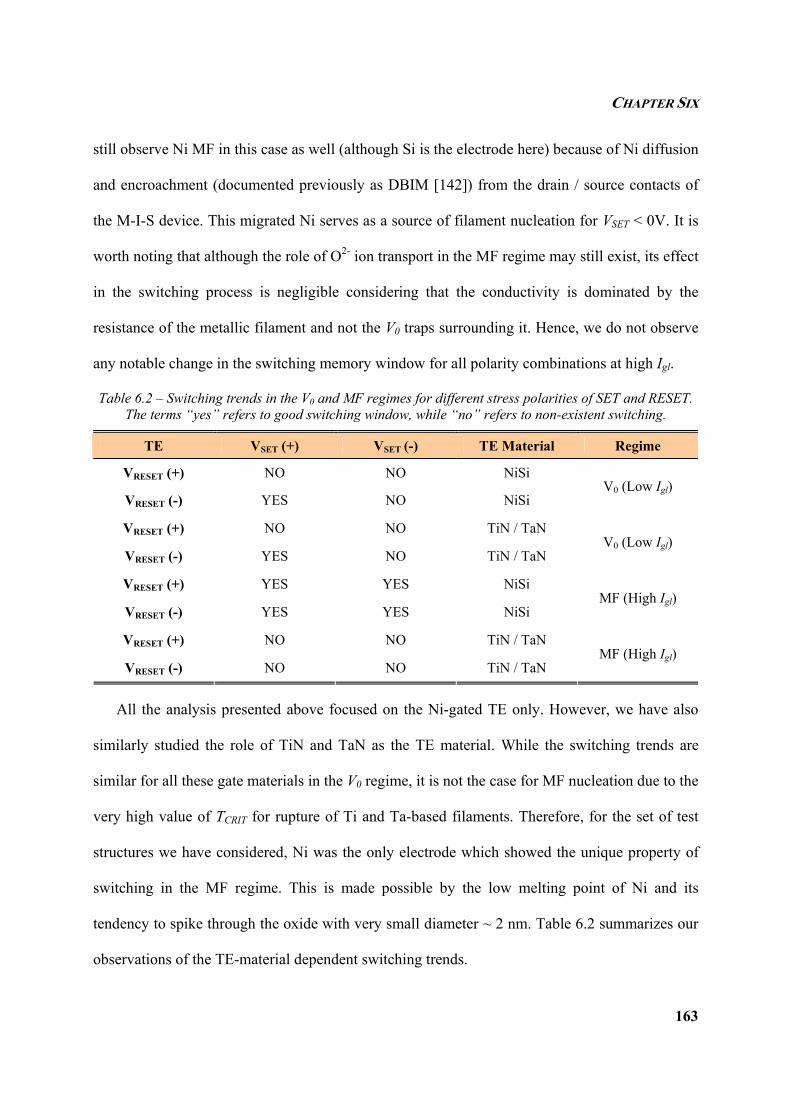
CHAPTER SIX
163
still observe Ni MF in this case as well (although Si is the electrode here) because of Ni diffusion
and encroachment (documented previously as DBIM [142]) from the drain / source contacts of
the M-I-S device. This migrated Ni serves as a source of filament nucleation for VSET < 0V. It is
worth noting that although the role of O2- ion transport in the MF regime may still exist, its effect
in the switching process is negligible considering that the conductivity is dominated by the
resistance of the metallic filament and not the V0 traps surrounding it. Hence, we do not observe
any notable change in the switching memory window for all polarity combinations at high Igl.
Table 6.2 – Switching trends in the V0 and MF regimes for different stress polarities of SET and RESET. The terms “yes” refers to good switching window, while “no” refers to non-existent switching.
TE VSET (+) VSET (-) TE Material Regime
VRESET (+) NO NO NiSi
VRESET (-) YES NO NiSi V0 (Low Igl)
VRESET (+) NO NO TiN / TaN
VRESET (-) YES NO TiN / TaN V0 (Low Igl)
VRESET (+) YES YES NiSi
VRESET (-) YES YES NiSi MF (High Igl)
VRESET (+) NO NO TiN / TaN
VRESET (-) NO NO TiN / TaN MF (High Igl)
All the analysis presented above focused on the Ni-gated TE only. However, we have also
similarly studied the role of TiN and TaN as the TE material. While the switching trends are
similar for all these gate materials in the V0 regime, it is not the case for MF nucleation due to the
very high value of TCRIT for rupture of Ti and Ta-based filaments. Therefore, for the set of test
structures we have considered, Ni was the only electrode which showed the unique property of
switching in the MF regime. This is made possible by the low melting point of Ni and its
tendency to spike through the oxide with very small diameter ~ 2 nm. Table 6.2 summarizes our
observations of the TE-material dependent switching trends.
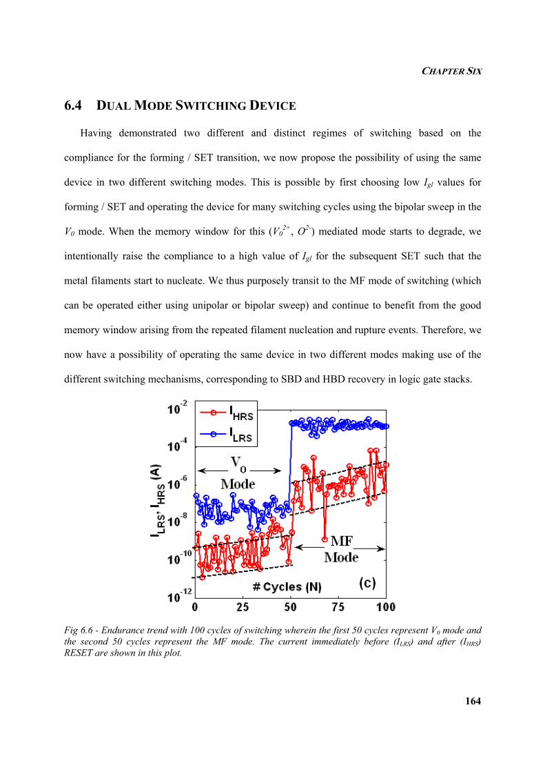
CHAPTER SIX
164
6.4 DUAL MODE SWITCHING DEVICE
Having demonstrated two different and distinct regimes of switching based on the
compliance for the forming / SET transition, we now propose the possibility of using the same
device in two different switching modes. This is possible by first choosing low Igl values for
forming / SET and operating the device for many switching cycles using the bipolar sweep in the
V0 mode. When the memory window for this (V02+, O2-) mediated mode starts to degrade, we
intentionally raise the compliance to a high value of Igl for the subsequent SET such that the
metal filaments start to nucleate. We thus purposely transit to the MF mode of switching (which
can be operated either using unipolar or bipolar sweep) and continue to benefit from the good
memory window arising from the repeated filament nucleation and rupture events. Therefore, we
now have a possibility of operating the same device in two different modes making use of the
different switching mechanisms, corresponding to SBD and HBD recovery in logic gate stacks.
Fig 6.6 - Endurance trend with 100 cycles of switching wherein the first 50 cycles represent V0 mode and the second 50 cycles represent the MF mode. The current immediately before (ILRS) and after (IHRS) RESET are shown in this plot.
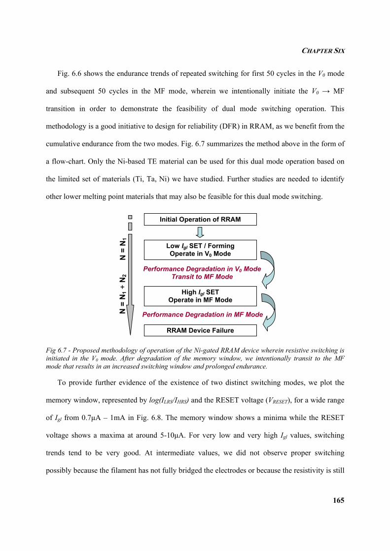
CHAPTER SIX
165
Fig. 6.6 shows the endurance trends of repeated switching for first 50 cycles in the V0 mode
and subsequent 50 cycles in the MF mode, wherein we intentionally initiate the V0 → MF
transition in order to demonstrate the feasibility of dual mode switching operation. This
methodology is a good initiative to design for reliability (DFR) in RRAM, as we benefit from the
cumulative endurance from the two modes. Fig. 6.7 summarizes the method above in the form of
a flow-chart. Only the Ni-based TE material can be used for this dual mode operation based on
the limited set of materials (Ti, Ta, Ni) we have studied. Further studies are needed to identify
other lower melting point materials that may also be feasible for this dual mode switching.
Fig 6.7 - Proposed methodology of operation of the Ni-gated RRAM device wherein resistive switching is initiated in the V0 mode. After degradation of the memory window, we intentionally transit to the MF mode that results in an increased switching window and prolonged endurance.
To provide further evidence of the existence of two distinct switching modes, we plot the
memory window, represented by log(ILRS/IHRS) and the RESET voltage (VRESET), for a wide range
of Igl from 0.7µA – 1mA in Fig. 6.8. The memory window shows a minima while the RESET
voltage shows a maxima at around 5-10µA. For very low and very high Igl values, switching
trends tend to be very good. At intermediate values, we did not observe proper switching
possibly because the filament has not fully bridged the electrodes or because the resistivity is still
Initial Operation of RRAM
Low Igl SET / Forming Operate in V0 Mode
High Igl SET Operate in MF Mode
RRAM Device Failure
Performance Degradation in V0 Mode Transit to MF Mode
N =
N1
Performance Degradation in MF Mode N =
N1 +
N2
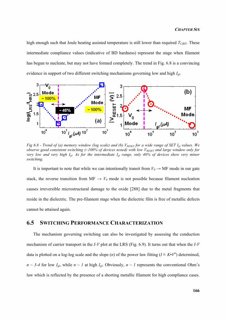
CHAPTER SIX
166
high enough such that Joule heating assisted temperature is still lower than required TCRIT. These
intermediate compliance values (indicative of BD hardness) represent the stage when filament
has begun to nucleate, but may not have formed completely. The trend in Fig. 6.8 is a convincing
evidence in support of two different switching mechanisms governing low and high Igl.
Fig 6.8 - Trend of (a) memory window (log scale) and (b) VRESET for a wide range of SET Igl values. We observe good consistent switching (~100% of devices tested) with low VRESET and large window only for very low and very high Igl. As for the intermediate Igl range, only 46% of devices show very minor switching.
It is important to note that while we can intentionally transit from V0 → MF mode in our gate
stack, the reverse transition from MF → V0 mode is not possible because filament nucleation
causes irreversible microstructural damage to the oxide [288] due to the metal fragments that
reside in the dielectric. The pre-filament stage when the dielectric film is free of metallic defects
cannot be attained again.
6.5 SWITCHING PERFORMANCE CHARACTERIZATION
The mechanism governing switching can also be investigated by assessing the conduction
mechanism of carrier transport in the I-V plot at the LRS (Fig. 6.9). It turns out that when the I-V
data is plotted on a log-log scale and the slope (n) of the power law fitting (I ≡ K•Vn) determined,
n ~ 3-4 for low Igl, while n ~ 1 at high Igl. Obviously, n ~ 1 represents the conventional Ohm’s
law which is reflected by the presence of a shorting metallic filament for high compliance cases.
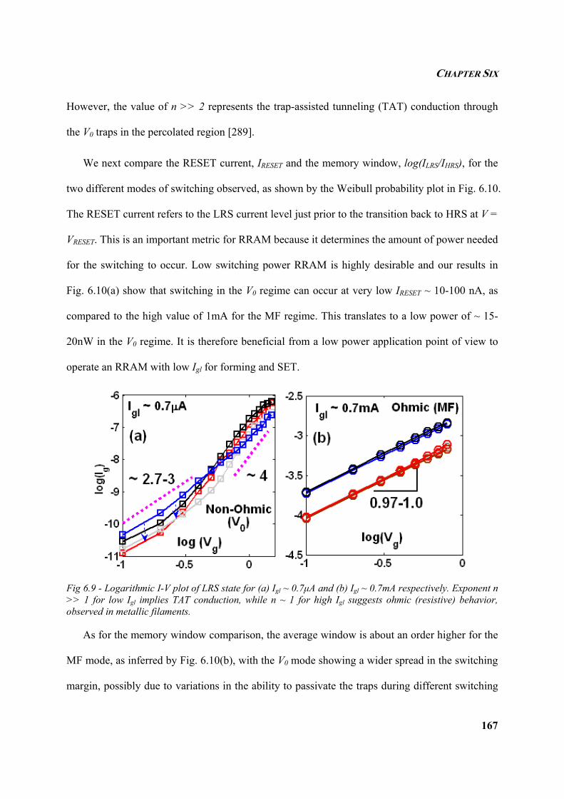
CHAPTER SIX
167
However, the value of n >> 2 represents the trap-assisted tunneling (TAT) conduction through
the V0 traps in the percolated region [289].
We next compare the RESET current, IRESET and the memory window, log(ILRS/IHRS), for the
two different modes of switching observed, as shown by the Weibull probability plot in Fig. 6.10.
The RESET current refers to the LRS current level just prior to the transition back to HRS at V =
VRESET. This is an important metric for RRAM because it determines the amount of power needed
for the switching to occur. Low switching power RRAM is highly desirable and our results in
Fig. 6.10(a) show that switching in the V0 regime can occur at very low IRESET ~ 10-100 nA, as
compared to the high value of 1mA for the MF regime. This translates to a low power of ~ 15-
20nW in the V0 regime. It is therefore beneficial from a low power application point of view to
operate an RRAM with low Igl for forming and SET.
Fig 6.9 - Logarithmic I-V plot of LRS state for (a) Igl ~ 0.7µA and (b) Igl ~ 0.7mA respectively. Exponent n >> 1 for low Igl implies TAT conduction, while n ~ 1 for high Igl suggests ohmic (resistive) behavior, observed in metallic filaments.
As for the memory window comparison, the average window is about an order higher for the
MF mode, as inferred by Fig. 6.10(b), with the V0 mode showing a wider spread in the switching
margin, possibly due to variations in the ability to passivate the traps during different switching
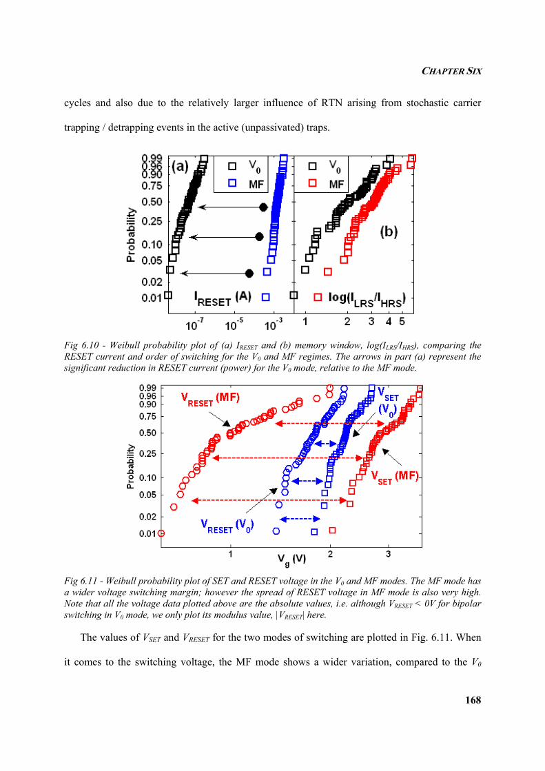
CHAPTER SIX
168
cycles and also due to the relatively larger influence of RTN arising from stochastic carrier
trapping / detrapping events in the active (unpassivated) traps.
Fig 6.10 - Weibull probability plot of (a) IRESET and (b) memory window, log(ILRS/IHRS), comparing the RESET current and order of switching for the V0 and MF regimes. The arrows in part (a) represent the significant reduction in RESET current (power) for the V0 mode, relative to the MF mode.
Fig 6.11 - Weibull probability plot of SET and RESET voltage in the V0 and MF modes. The MF mode has a wider voltage switching margin; however the spread of RESET voltage in MF mode is also very high. Note that all the voltage data plotted above are the absolute values, i.e. although VRESET < 0V for bipolar switching in V0 mode, we only plot its modulus value, |VRESET| here.
The values of VSET and VRESET for the two modes of switching are plotted in Fig. 6.11. When
it comes to the switching voltage, the MF mode shows a wider variation, compared to the V0
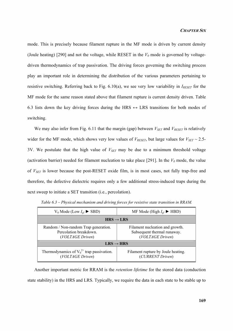
CHAPTER SIX
169
mode. This is precisely because filament rupture in the MF mode is driven by current density
(Joule heating) [290] and not the voltage, while RESET in the V0 mode is governed by voltage-
driven thermodynamics of trap passivation. The driving forces governing the switching process
play an important role in determining the distribution of the various parameters pertaining to
resistive switching. Referring back to Fig. 6.10(a), we see very low variability in IRESET for the
MF mode for the same reason stated above that filament rupture is current density driven. Table
6.3 lists down the key driving forces during the HRS ↔ LRS transitions for both modes of
switching.
We may also infer from Fig. 6.11 that the margin (gap) between VSET and VRESET is relatively
wider for the MF mode, which shows very low values of VRESET, but large values for VSET ~ 2.5-
3V. We postulate that the high value of VSET may be due to a minimum threshold voltage
(activation barrier) needed for filament nucleation to take place [291]. In the V0 mode, the value
of VSET is lower because the post-RESET oxide film, is in most cases, not fully trap-free and
therefore, the defective dielectric requires only a few additional stress-induced traps during the
next sweep to initiate a SET transition (i.e., percolation).
Table 6.3 – Physical mechanism and driving forces for resistive state transition in RRAM.
V0 Mode (Low Igl SBD) MF Mode (High Igl HBD)
HRS → LRS
Random / Non-random Trap generation. Percolation breakdown.
(VOLTAGE Driven)
Filament nucleation and growth. Subsequent thermal runaway.
(VOLTAGE Driven) LRS → HRS
Thermodynamics of V02+ trap passivation.
(VOLTAGE Driven) Filament rupture by Joule heating.
(CURRENT Driven)
Another important metric for RRAM is the retention lifetime for the stored data (conduction
state stability) in the HRS and LRS. Typically, we require the data in each state to be stable up to
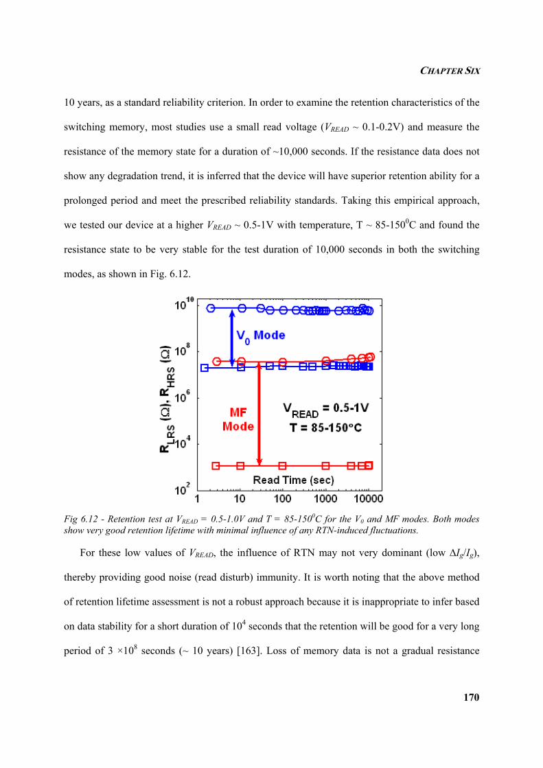
CHAPTER SIX
170
10 years, as a standard reliability criterion. In order to examine the retention characteristics of the
switching memory, most studies use a small read voltage (VREAD ~ 0.1-0.2V) and measure the
resistance of the memory state for a duration of ~10,000 seconds. If the resistance data does not
show any degradation trend, it is inferred that the device will have superior retention ability for a
prolonged period and meet the prescribed reliability standards. Taking this empirical approach,
we tested our device at a higher VREAD ~ 0.5-1V with temperature, T ~ 85-1500C and found the
resistance state to be very stable for the test duration of 10,000 seconds in both the switching
modes, as shown in Fig. 6.12.
Fig 6.12 - Retention test at VREAD = 0.5-1.0V and T = 85-1500C for the V0 and MF modes. Both modes show very good retention lifetime with minimal influence of any RTN-induced fluctuations.
For these low values of VREAD, the influence of RTN may not very dominant (low ∆Ig/Ig),
thereby providing good noise (read disturb) immunity. It is worth noting that the above method
of retention lifetime assessment is not a robust approach because it is inappropriate to infer based
on data stability for a short duration of 104 seconds that the retention will be good for a very long
period of 3 ×10⁸ seconds (~ 10 years) [163]. Loss of memory data is not a gradual resistance
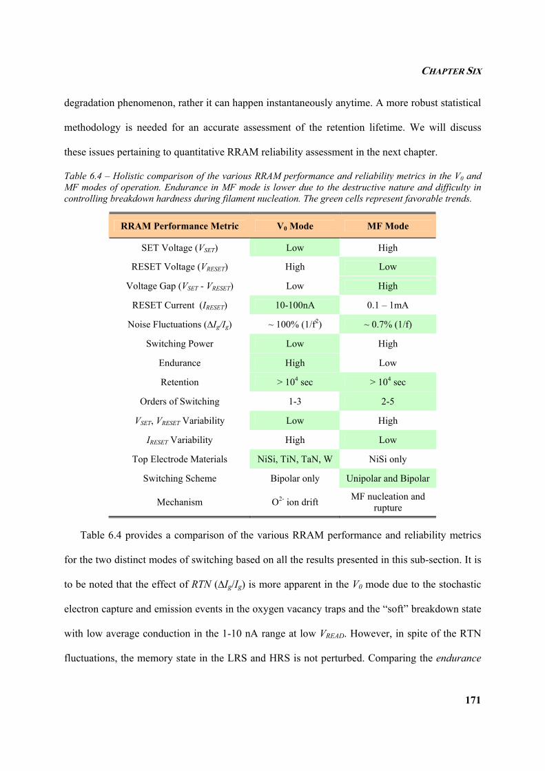
CHAPTER SIX
171
degradation phenomenon, rather it can happen instantaneously anytime. A more robust statistical
methodology is needed for an accurate assessment of the retention lifetime. We will discuss
these issues pertaining to quantitative RRAM reliability assessment in the next chapter.
Table 6.4 – Holistic comparison of the various RRAM performance and reliability metrics in the V0 and MF modes of operation. Endurance in MF mode is lower due to the destructive nature and difficulty in controlling breakdown hardness during filament nucleation. The green cells represent favorable trends.
RRAM Performance Metric V0 Mode MF Mode
SET Voltage (VSET) Low High
RESET Voltage (VRESET) High Low
Voltage Gap (VSET - VRESET) Low High
RESET Current (IRESET) 10-100nA 0.1 – 1mA
Noise Fluctuations (∆Ig/Ig) ~ 100% (1/f2) ~ 0.7% (1/f)
Switching Power Low High
Endurance High Low
Retention > 104 sec > 104 sec
Orders of Switching 1-3 2-5
VSET, VRESET Variability Low High
IRESET Variability High Low
Top Electrode Materials NiSi, TiN, TaN, W NiSi only
Switching Scheme Bipolar only Unipolar and Bipolar
Mechanism O2- ion drift MF nucleation and rupture
Table 6.4 provides a comparison of the various RRAM performance and reliability metrics
for the two distinct modes of switching based on all the results presented in this sub-section. It is
to be noted that the effect of RTN (∆Ig/Ig) is more apparent in the V0 mode due to the stochastic
electron capture and emission events in the oxygen vacancy traps and the “soft” breakdown state
with low average conduction in the 1-10 nA range at low VREAD. However, in spite of the RTN
fluctuations, the memory state in the LRS and HRS is not perturbed. Comparing the endurance
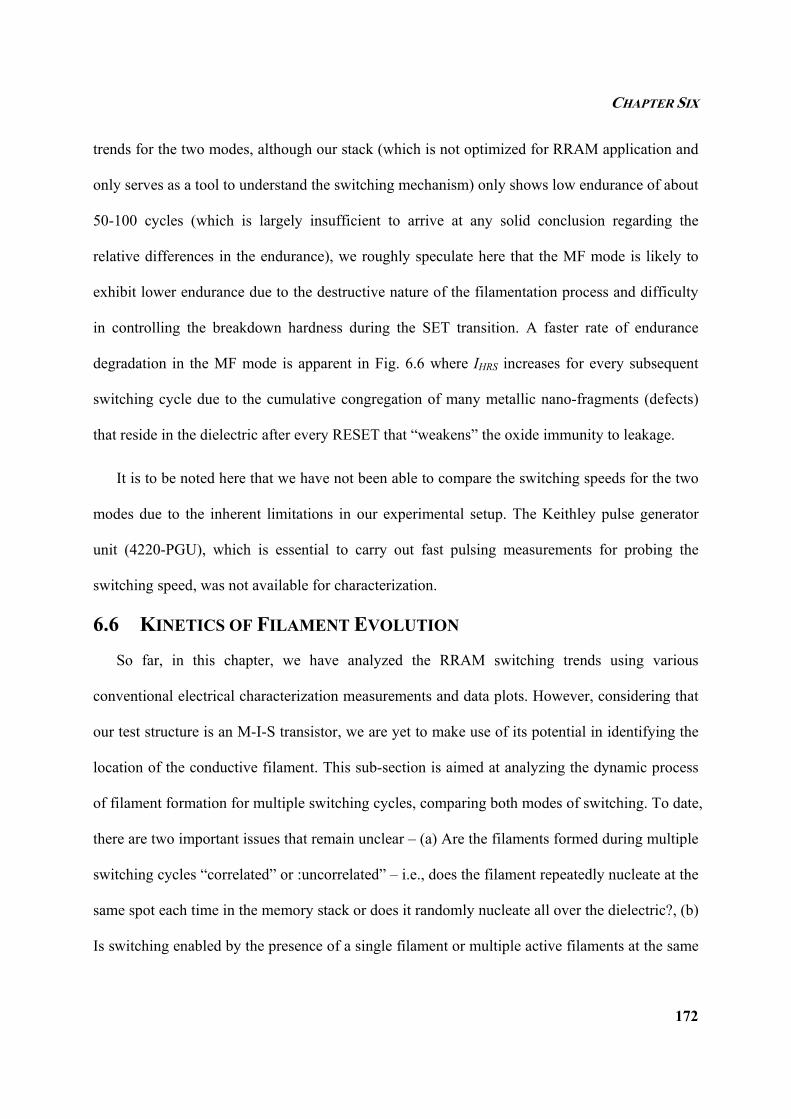
CHAPTER SIX
172
trends for the two modes, although our stack (which is not optimized for RRAM application and
only serves as a tool to understand the switching mechanism) only shows low endurance of about
50-100 cycles (which is largely insufficient to arrive at any solid conclusion regarding the
relative differences in the endurance), we roughly speculate here that the MF mode is likely to
exhibit lower endurance due to the destructive nature of the filamentation process and difficulty
in controlling the breakdown hardness during the SET transition. A faster rate of endurance
degradation in the MF mode is apparent in Fig. 6.6 where IHRS increases for every subsequent
switching cycle due to the cumulative congregation of many metallic nano-fragments (defects)
that reside in the dielectric after every RESET that “weakens” the oxide immunity to leakage.
It is to be noted here that we have not been able to compare the switching speeds for the two
modes due to the inherent limitations in our experimental setup. The Keithley pulse generator
unit (4220-PGU), which is essential to carry out fast pulsing measurements for probing the
switching speed, was not available for characterization.
6.6 KINETICS OF FILAMENT EVOLUTION
So far, in this chapter, we have analyzed the RRAM switching trends using various
conventional electrical characterization measurements and data plots. However, considering that
our test structure is an M-I-S transistor, we are yet to make use of its potential in identifying the
location of the conductive filament. This sub-section is aimed at analyzing the dynamic process
of filament formation for multiple switching cycles, comparing both modes of switching. To date,
there are two important issues that remain unclear – (a) Are the filaments formed during multiple
switching cycles “correlated” or :uncorrelated” – i.e., does the filament repeatedly nucleate at the
same spot each time in the memory stack or does it randomly nucleate all over the dielectric?, (b)
Is switching enabled by the presence of a single filament or multiple active filaments at the same
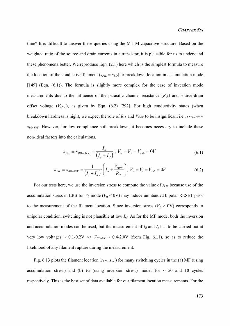
CHAPTER SIX
173
time? It is difficult to answer these queries using the M-I-M capacitive structure. Based on the
weighted ratio of the source and drain currents in a transistor, it is plausible for us to understand
these phenomena better. We reproduce Eqn. (2.1) here which is the simplest formula to measure
the location of the conductive filament (sFIL ≡ sBD) or breakdown location in accumulation mode
[149] (Eqn. (6.1)). The formula is slightly more complex for the case of inversion mode
measurements due to the influence of the parasitic channel resistance (Rch) and source-drain
offset voltage (VOFF), as given by Eqn. (6.2) [292]. For high conductivity states (when
breakdown hardness is high), we expect the role of Rch and VOFF to be insignificant i.e., sBD-ACC ~
sBD-INV. However, for low compliance soft breakdown, it becomes necessary to include these
non-ideal factors into the calculations.
( ) VVVV;II
Iss subsdds
dACCBDFIL 0===
+=≡ − (6.1)
( ) VVVV;R
VIII
ss subsdch
OFFd
dsINVBDFIL 01
===⎟⎟⎠
⎞⎜⎜⎝
⎛+⋅
+=≡ − (6.2)
For our tests here, we use the inversion stress to compute the value of sFIL because use of the
accumulation stress in LRS for V0 mode (Vg < 0V) may induce unintended bipolar RESET prior
to the measurement of the filament location. Since inversion stress (Vg > 0V) corresponds to
unipolar condition, switching is not plausible at low Igl. As for the MF mode, both the inversion
and accumulation modes can be used, but the measurement of Id and Is has to be carried out at
very low voltages ~ 0.1-0.2V << VRESET ~ 0.4-2.0V (from Fig. 6.11), so as to reduce the
likelihood of any filament rupture during the measurement.
Fig. 6.13 plots the filament location (sFIL, sBD) for many switching cycles in the (a) MF (using
accumulation stress) and (b) V0 (using inversion stress) modes for ~ 50 and 10 cycles
respectively. This is the best set of data available for our filament location measurements. For the
CHAPTER SIX
174
MF mode, we observe various clusters of data indicating that the filaments tend to nucleate at
their previously ruptured locations in many cases. Only when the filament undergoes complete
rupture (this event is of low probability) for a particular switching cycle do we observe a change
in filament location for subsequent switching events. We can therefore call the filamentation
process in MF mode as “pseudo-random”.
Fig 6.13 - Variation of the conductive filament (BD) location along the M-I-S transistor structure channel for ~50 and ~10 cycles of switching in the (a) MF and (b) V0 modes respectively. Clusters of data for the sFIL location in MF mode imply “pseudo-random” and “correlated” nature of filament nucleation. As for the V0 mode, filament nucleation is purely “random” and “uncorrelated”.
For the V0 mode, the evolution of filament location seems to be “fully random” with no clear
evidence of correlation. This however depends very much on the maximum RESET stop voltage
used in the bipolar sweep process. If the maximum VRESET is small, not all the traps in the
percolated region can be passivated, which may lead to subsequent breakdown events being
triggered at the same location. For all our device tests, we set the maximum VRESET to around
-(2.35-2.50)V, which is sufficiently high to enable most of the traps to be passivated. Fig. 6.14
illustrates the above explanation for the pseudo-random and random nature of multiple switching
CHAPTER SIX
175
cycle filament evolution. We observe the MF mode filaments to favorably nucleate at the corners
of the transistor due to the defective interface between high-κ and spacer there [145, 293] and
also due to the electric field enhancement at the corner regions.
Fig 6.14 – Illustration showing the (a) increased efficiency in passivation of oxygen vacancy traps for higher bipolar VRESET in the V0 mode and (b) the partial and fully ruptured filaments in the MF mode which cause the “pseudo-random” nature of filamentation process. In the case of a partially ruptured metal filament, the electric-field across the ruptured region during the next SET cycle is sufficiently high such that it becomes favorable for the ruptured filament to nucleate again. This is more so the case if the ruptured filament is sharply pointed due to the lightning rod effect [294].
6.7 INTERESTING DESIGN APPLICATIONS OF OUR TEST STRUCTURE
Having presented a complete suite of electrical measurements on the resistive switching
mechanism in M-I-S transistor based test structures, let us now discuss the potential applications
and uniqueness of such a test structure for RRAM application. It turns out that switching in a
transistor stack provides us with many interesting RRAM design possibilities and eases the
implementation and commercialization of this simple NVM architecture for future
semiconductor technology. Some of the advantages and design options are discussed below.
NiSi
p-Si
O2-
V02+
O2- NiSi
DBIM DBIM
(b) (a)
V0 Mode Metal Filament Mode
Passivated Traps Active Traps
VRESET Partial
Rupture p-Si
Complete Rupture
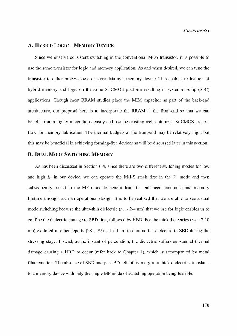
CHAPTER SIX
176
A. HYBRID LOGIC – MEMORY DEVICE
Since we observe consistent switching in the conventional MOS transistor, it is possible to
use the same transistor for logic and memory application. As and when desired, we can tune the
transistor to either process logic or store data as a memory device. This enables realization of
hybrid memory and logic on the same Si CMOS platform resulting in system-on-chip (SoC)
applications. Though most RRAM studies place the MIM capacitor as part of the back-end
architecture, our proposal here is to incorporate the RRAM at the front-end so that we can
benefit from a higher integration density and use the existing well-optimized Si CMOS process
flow for memory fabrication. The thermal budgets at the front-end may be relatively high, but
this may be beneficial in achieving forming-free devices as will be discussed later in this section.
B. DUAL MODE SWITCHING MEMORY
As has been discussed in Section 6.4, since there are two different switching modes for low
and high Igl in our device, we can operate the M-I-S stack first in the V0 mode and then
subsequently transit to the MF mode to benefit from the enhanced endurance and memory
lifetime through such an operational design. It is to be realized that we are able to see a dual
mode switching because the ultra-thin dielectric (tox ~ 2-4 nm) that we use for logic enables us to
confine the dielectric damage to SBD first, followed by HBD. For the thick dielectrics (tox ~ 7-10
nm) explored in other reports [281, 295], it is hard to confine the dielectric to SBD during the
stressing stage. Instead, at the instant of percolation, the dielectric suffers substantial thermal
damage causing a HBD to occur (refer back to Chapter 1), which is accompanied by metal
filamentation. The absence of SBD and post-BD reliability margin in thick dielectrics translates
to a memory device with only the single MF mode of switching operation being feasible.
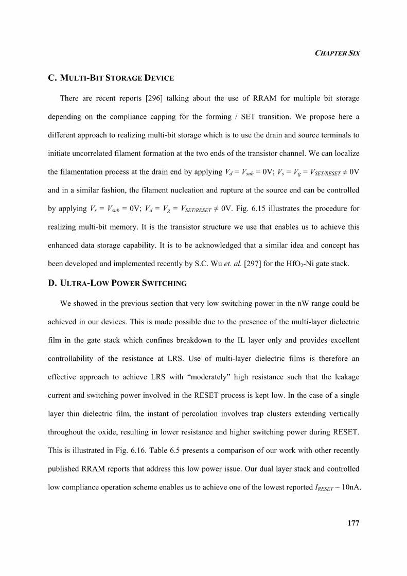
CHAPTER SIX
177
C. MULTI-BIT STORAGE DEVICE
There are recent reports [296] talking about the use of RRAM for multiple bit storage
depending on the compliance capping for the forming / SET transition. We propose here a
different approach to realizing multi-bit storage which is to use the drain and source terminals to
initiate uncorrelated filament formation at the two ends of the transistor channel. We can localize
the filamentation process at the drain end by applying Vd = Vsub = 0V; Vs = Vg = VSET/RESET ≠ 0V
and in a similar fashion, the filament nucleation and rupture at the source end can be controlled
by applying Vs = Vsub = 0V; Vd = Vg = VSET/RESET ≠ 0V. Fig. 6.15 illustrates the procedure for
realizing multi-bit memory. It is the transistor structure we use that enables us to achieve this
enhanced data storage capability. It is to be acknowledged that a similar idea and concept has
been developed and implemented recently by S.C. Wu et. al. [297] for the HfO2-Ni gate stack.
D. ULTRA-LOW POWER SWITCHING
We showed in the previous section that very low switching power in the nW range could be
achieved in our devices. This is made possible due to the presence of the multi-layer dielectric
film in the gate stack which confines breakdown to the IL layer only and provides excellent
controllability of the resistance at LRS. Use of multi-layer dielectric films is therefore an
effective approach to achieve LRS with “moderately” high resistance such that the leakage
current and switching power involved in the RESET process is kept low. In the case of a single
layer thin dielectric film, the instant of percolation involves trap clusters extending vertically
throughout the oxide, resulting in lower resistance and higher switching power during RESET.
This is illustrated in Fig. 6.16. Table 6.5 presents a comparison of our work with other recently
published RRAM reports that address this low power issue. Our dual layer stack and controlled
low compliance operation scheme enables us to achieve one of the lowest reported IRESET ~ 10nA.
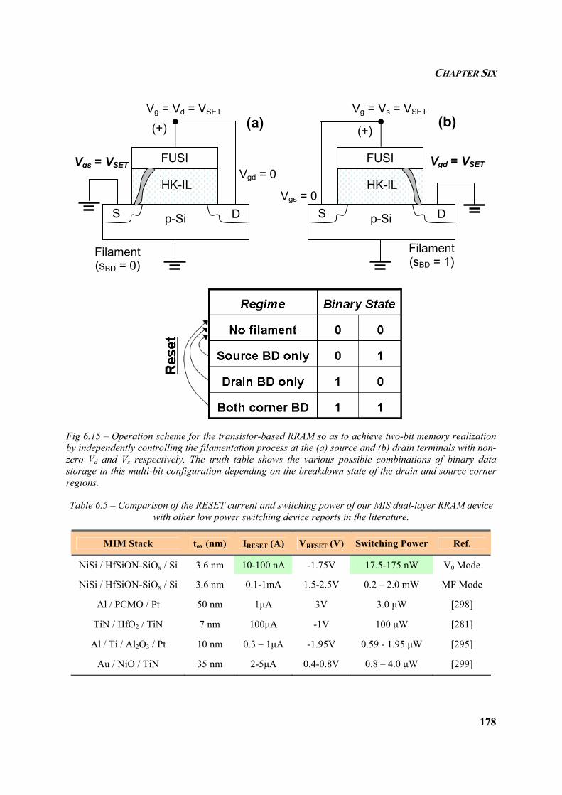
CHAPTER SIX
178
Fig 6.15 – Operation scheme for the transistor-based RRAM so as to achieve two-bit memory realization by independently controlling the filamentation process at the (a) source and (b) drain terminals with non-zero Vd and Vs respectively. The truth table shows the various possible combinations of binary data storage in this multi-bit configuration depending on the breakdown state of the drain and source corner regions.
Table 6.5 – Comparison of the RESET current and switching power of our MIS dual-layer RRAM device with other low power switching device reports in the literature.
MIM Stack tox (nm) IRESET (A) VRESET (V) Switching Power Ref.
NiSi / HfSiON-SiOx / Si 3.6 nm 10-100 nA -1.75V 17.5-175 nW V0 Mode
NiSi / HfSiON-SiOx / Si 3.6 nm 0.1-1mA 1.5-2.5V 0.2 – 2.0 mW MF Mode
Al / PCMO / Pt 50 nm 1µA 3V 3.0 µW [298]
TiN / HfO2 / TiN 7 nm 100µA -1V 100 µW [281]
Al / Ti / Al2O3 / Pt 10 nm 0.3 – 1µA -1.95V 0.59 - 1.95 µW [295]
Au / NiO / TiN 35 nm 2-5µA 0.4-0.8V 0.8 – 4.0 µW [299]
FUSI
p-Si DS
HK-IL
Vg = Vd = VSET (+)
Filament (sBD = 0)
Vgd = 0 Vgs = VSET FUSI
p-Si D S
HK-IL
Vg = Vs = VSET
(+)
Filament (sBD = 1)
Vgd = VSET
Vgs = 0
(a) (b)
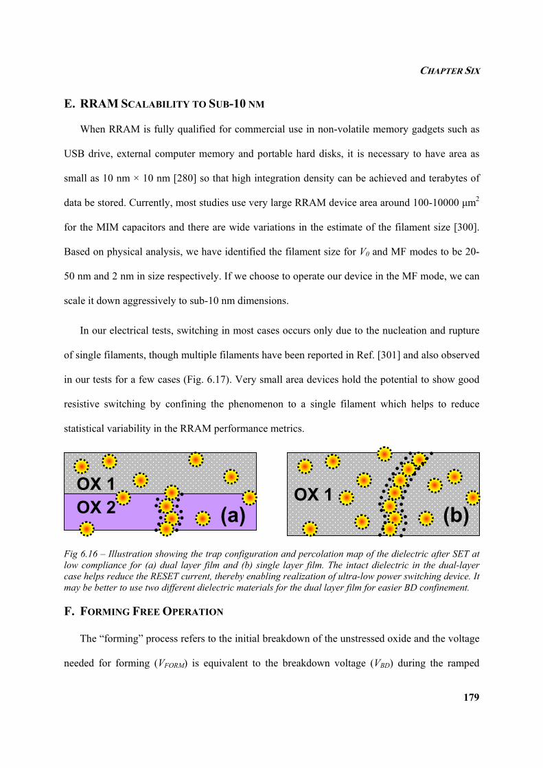
CHAPTER SIX
179
E. RRAM SCALABILITY TO SUB-10 NM
When RRAM is fully qualified for commercial use in non-volatile memory gadgets such as
USB drive, external computer memory and portable hard disks, it is necessary to have area as
small as 10 nm × 10 nm [280] so that high integration density can be achieved and terabytes of
data be stored. Currently, most studies use very large RRAM device area around 100-10000 µm2
for the MIM capacitors and there are wide variations in the estimate of the filament size [300].
Based on physical analysis, we have identified the filament size for V0 and MF modes to be 20-
50 nm and 2 nm in size respectively. If we choose to operate our device in the MF mode, we can
scale it down aggressively to sub-10 nm dimensions.
In our electrical tests, switching in most cases occurs only due to the nucleation and rupture
of single filaments, though multiple filaments have been reported in Ref. [301] and also observed
in our tests for a few cases (Fig. 6.17). Very small area devices hold the potential to show good
resistive switching by confining the phenomenon to a single filament which helps to reduce
statistical variability in the RRAM performance metrics.
Fig 6.16 – Illustration showing the trap configuration and percolation map of the dielectric after SET at low compliance for (a) dual layer film and (b) single layer film. The intact dielectric in the dual-layer case helps reduce the RESET current, thereby enabling realization of ultra-low power switching device. It may be better to use two different dielectric materials for the dual layer film for easier BD confinement.
F. FORMING FREE OPERATION
The “forming” process refers to the initial breakdown of the unstressed oxide and the voltage
needed for forming (VFORM) is equivalent to the breakdown voltage (VBD) during the ramped
OX 2 OX 1
OX 1
(a) (b)
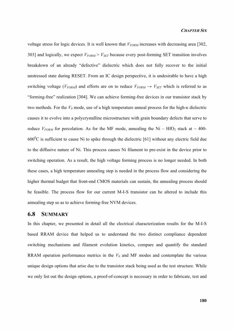
CHAPTER SIX
180
voltage stress for logic devices. It is well known that VFORM increases with decreasing area [302,
303] and logically, we expect VFORM > VSET because every post-forming SET transition involves
breakdown of an already “defective” dielectric which does not fully recover to the initial
unstressed state during RESET. From an IC design perspective, it is undesirable to have a high
switching voltage (VFORM) and efforts are on to reduce VFORM → VSET which is referred to as
“forming-free” realization [304]. We can achieve forming-free devices in our transistor stack by
two methods. For the V0 mode, use of a high temperature anneal process for the high-κ dielectric
causes it to evolve into a polycrystalline microstructure with grain boundary defects that serve to
reduce VFORM for percolation. As for the MF mode, annealing the Ni – HfO2 stack at ~ 400-
6000C is sufficient to cause Ni to spike through the dielectric [61] without any electric field due
to the diffusive nature of Ni. This process causes Ni filament to pre-exist in the device prior to
switching operation. As a result, the high voltage forming process is no longer needed. In both
these cases, a high temperature annealing step is needed in the process flow and considering the
higher thermal budget that front-end CMOS materials can sustain, the annealing process should
be feasible. The process flow for our current M-I-S transistor can be altered to include this
annealing step so as to achieve forming-free NVM devices.
6.8 SUMMARY
In this chapter, we presented in detail all the electrical characterization results for the M-I-S
based RRAM device that helped us to understand the two distinct compliance dependent
switching mechanisms and filament evolution kinetics, compare and quantify the standard
RRAM operation performance metrics in the V0 and MF modes and contemplate the various
unique design options that arise due to the transistor stack being used as the test structure. While
we only list out the design options, a proof-of-concept is necessary in order to fabricate, test and
CHAPTER SIX
181
optimize each of these novel proposals to assess their practical technological feasibility as an
effective solution. Due to bandwidth limitations, we refrain from pursuing these ideas any further
in the context of this study.
Fig 6.17 – Possibility of multiple stages of RESET in the MF mode suggest the possibility of existence of multiple filaments in the 0.15µm2 area devices tested. However, aggressive scaling of the device to 10 nm × 10 nm may lead us into single filament based switching operation.
On the whole, our M-I-S stack has proven to be an effective tool in realizing multi-bit memory
devices, as was discussed earlier in detail. What remains to be investigated is the reliability of
each of the switching modes in our gate stack. Reliability for an NVM device refers to the (a)
retention lifetime, (b) endurance and (c) read disturb noise immunity. We aim to present a
convincing study on the reliability of the RRAM from a quantitative physical and
thermodynamic point of view in the next chapter so that current limitations in the use of accurate
reliability methodologies for NVM qualification are overcome.
CHAPTER SEVEN
182
CHAPTER SEVEN
RRREEELLLIIIAAABBBIIILLLIIITTTYYY MMMEEETTTRRRIIICCCSSS FFFOOORRR SSSWWWIIITTTCCCHHHIIINNNGGG MMMEEEMMMOOORRRYYY
7.1 INTRODUCTION
The previous chapter focused on the performance metrics for switching memory including
quantitative assessment of SET and RESET voltage, RESET current, switching power, memory
window and their variation. Although we have earlier presented some electrical test results on
the retention lifetime, a detailed study on the reliability aspects of switching memory and the
driving forces for degradation of the memory device is necessary in order to assess the feasibility
of the RRAM for commercial use as the next generation feasible data storage technology. Any
new device with high performance but low reliability would dampen the prospects of its
implementation. With this motive, we shall study the three different reliability metrics for
RRAM based on our M-I-S transistor structure. They are (a) retention in the HRS and LRS, (b)
endurance in both states and (c) read disturb immunity, which is equivalent to random telegraph
noise (RTN) studies in logic gate stacks. The reliability in both the switching modes (V0 and MF)
will be assessed in this chapter.
7.2 RETENTION LIFETIME
Retention is an important performance metric for RRAM devices referring to the unperturbed
state of data storage or stability of the resistance state to externally induced fluctuations (voltage,
temperature). Instead of testing the device at very low VREAD ~ 0.1V for a short duration of
10,000 seconds and arbitrarily considering this to be sufficient evidence for 10 year lifetime, as
speculated in many reports [305, 306], we aim to quantify the retention duration more accurately.
CHAPTER SEVEN
183
Considering that the V0 mode of switching involves the generation of traps during the
forming /SET transition until percolation is observed, we make use of the concept of percolation
and its relation to the TDDB failure to study the HRS retention lifetime. Following this, we focus
on the LRS state, where the drift and diffusion [307, 308] as well as the reaction kinetics of the
trap passivation process are the key driving forces that govern the movement of the mobile O2-
ions and hence the retention.
For the MF mode of switching, we consider the ramp rate dependencies of VSET and VRESET,
which gives us some interesting inferences on the existence of a “threshold voltage (VTH)” for
change in memory state. In other words, if VREAD < VTH, we may consider the retention time to be
“theoretically infinite”, similar in ideology to the concept of critical voltage (Vcrit) for dielectric
post-BD degradation presented earlier in Chapter 3. Let us now consider each of these cases in
detail and assess the robustness of our M-I-S stack for memory state stability.
7.2.1 HRS RETENTION IN OXYGEN VACANCY MODE
The change of filament location (sFIL) for multiple switching cycles is shown in Fig. 7.1(b)
(this is a reproduced figure from Chapter 6), based on the inversion mode S/D current
measurement setup as illustrated in Fig. 7.1(a). Since the sFIL varies randomly between the source
and drain, we can confirm that in general, majority of the SET transitions are “uncorrelated”
events, in which case, we should expect the percolation model and Weibull statistics to be
applicable for predicting the retention lifetime at the HRS. To confirm this, we performed
repeated switching measurements on another device which showed N = 50 consistent cycles of
switching and noted down the VSET values, which we plot as a function of N in Fig. 7.2(a). The
VSET values are randomly scattered with no clear trend of reduction with increasing N. If the
switching event induced accumulative damage to the dielectric (for example in terms of
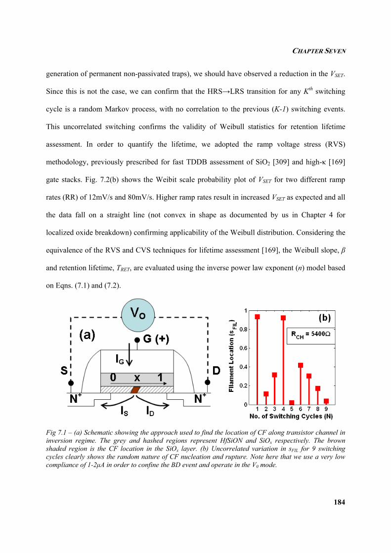
CHAPTER SEVEN
184
generation of permanent non-passivated traps), we should have observed a reduction in the VSET.
Since this is not the case, we can confirm that the HRS→LRS transition for any Kth switching
cycle is a random Markov process, with no correlation to the previous (K-1) switching events.
This uncorrelated switching confirms the validity of Weibull statistics for retention lifetime
assessment. In order to quantify the lifetime, we adopted the ramp voltage stress (RVS)
methodology, previously prescribed for fast TDDB assessment of SiO2 [309] and high-κ [169]
gate stacks. Fig. 7.2(b) shows the Weibit scale probability plot of VSET for two different ramp
rates (RR) of 12mV/s and 80mV/s. Higher ramp rates result in increased VSET as expected and all
the data fall on a straight line (not convex in shape as documented by us in Chapter 4 for
localized oxide breakdown) confirming applicability of the Weibull distribution. Considering the
equivalence of the RVS and CVS techniques for lifetime assessment [169], the Weibull slope, β
and retention lifetime, TRET, are evaluated using the inverse power law exponent (n) model based
on Eqns. (7.1) and (7.2).
Fig 7.1 – (a) Schematic showing the approach used to find the location of CF along transistor channel in inversion regime. The grey and hashed regions represent HfSiON and SiOx respectively. The brown shaded region is the CF location in the SiOx layer. (b) Uncorrelated variation in sFIL for 9 switching cycles clearly shows the random nature of CF nucleation and rupture. Note here that we use a very low compliance of 1-2µA in order to confine the BD event and operate in the V0 mode.
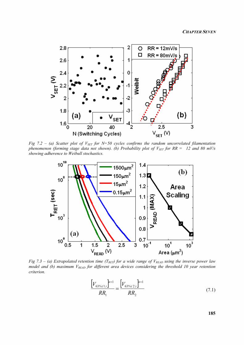
CHAPTER SEVEN
185
Fig 7.2 – (a) Scatter plot of VSET for N=50 cycles confirms the random uncorrelated filamentation phenomenon (forming stage data not shown). (b) Probability plot of VSET for RR = 12 and 80 mV/s showing adherence to Weibull stochastics.
Fig 7.3 – (a) Extrapolated retention time (TRET) for a wide range of VREAD using the inverse power law model and (b) maximum VREAD for different area devices considering the threshold 10 year retention criterion.
[ ] [ ]
2
1263
1
1163
RRV
RRV n
)(%n
)(%++
= (7.1)
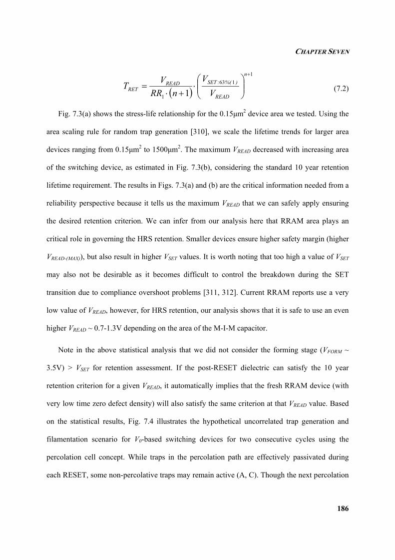
CHAPTER SEVEN
186
( )
1163
1 1
+
⎟⎟⎠
⎞⎜⎜⎝
⎛⋅
+⋅=
n
READ
)%(:SETREADRET V
VnRR
VT (7.2)
Fig. 7.3(a) shows the stress-life relationship for the 0.15µm2 device area we tested. Using the
area scaling rule for random trap generation [310], we scale the lifetime trends for larger area
devices ranging from 0.15µm2 to 1500µm2. The maximum VREAD decreased with increasing area
of the switching device, as estimated in Fig. 7.3(b), considering the standard 10 year retention
lifetime requirement. The results in Figs. 7.3(a) and (b) are the critical information needed from a
reliability perspective because it tells us the maximum VREAD that we can safely apply ensuring
the desired retention criterion. We can infer from our analysis here that RRAM area plays an
critical role in governing the HRS retention. Smaller devices ensure higher safety margin (higher
VREAD-(MAX)), but also result in higher VSET values. It is worth noting that too high a value of VSET
may also not be desirable as it becomes difficult to control the breakdown during the SET
transition due to compliance overshoot problems [311, 312]. Current RRAM reports use a very
low value of VREAD, however, for HRS retention, our analysis shows that it is safe to use an even
higher VREAD ~ 0.7-1.3V depending on the area of the M-I-M capacitor.
Note in the above statistical analysis that we did not consider the forming stage (VFORM ~
3.5V) > VSET for retention assessment. If the post-RESET dielectric can satisfy the 10 year
retention criterion for a given VREAD, it automatically implies that the fresh RRAM device (with
very low time zero defect density) will also satisfy the same criterion at that VREAD value. Based
on the statistical results, Fig. 7.4 illustrates the hypothetical uncorrelated trap generation and
filamentation scenario for V0-based switching devices for two consecutive cycles using the
percolation cell concept. While traps in the percolation path are effectively passivated during
each RESET, some non-percolative traps may remain active (A, C). Though the next percolation
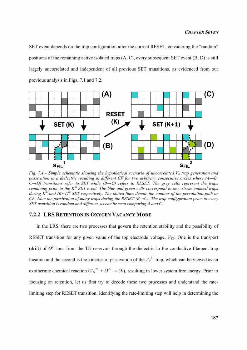
CHAPTER SEVEN
187
SET event depends on the trap configuration after the current RESET, considering the “random”
positions of the remaining active isolated traps (A, C), every subsequent SET event (B, D) is still
largely uncorrelated and independent of all previous SET transitions, as evidenced from our
previous analysis in Figs. 7.1 and 7.2.
Fig. 7.4 - Simple schematic showing the hypothetical scenario of uncorrelated V0 trap generation and passivation in a dielectric resulting in different CF for two arbitrary consecutive cycles where (A→B; C→D) transitions refer to SET while (B→C) refers to RESET. The grey cells represent the traps remaining prior to the Kth SET event. The blue and green cells correspond to new stress induced traps during Kth and (K+1)th SET respectively. The dotted lines denote the contour of the percolation path or CF. Note the passivation of many traps during the RESET (B→C). The trap configuration prior to every SET transition is random and different, as can be seen comparing A and C.
7.2.2 LRS RETENTION IN OXYGEN VACANCY MODE
In the LRS, there are two processes that govern the retention stability and the possibility of
RESET transition for any given value of the top electrode voltage, VTE. One is the transport
(drift) of O2- ions from the TE reservoir through the dielectric to the conductive filament trap
location and the second is the kinetics of passivation of the V02+ trap, which can be viewed as an
exothermic chemical reaction (VO2+ + O2- → O0), resulting in lower system free energy. Prior to
focusing on retention, let us first try to decode these two processes and understand the rate-
limiting step for RESET transition. Identifying the rate-limiting step will help in determining the
(A)
(B)
(C)
(D)
sFIL1 sFIL
2
SET (K) SET (K+1)
RESET (K)
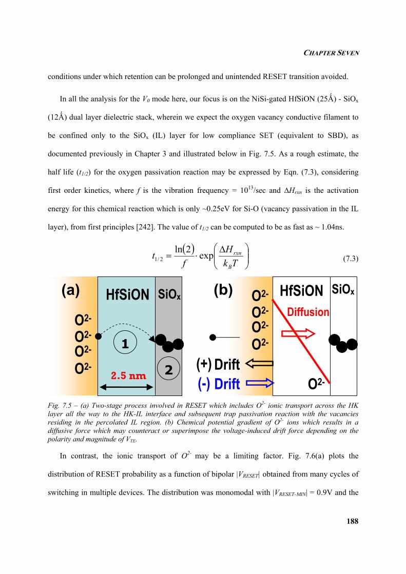
CHAPTER SEVEN
188
conditions under which retention can be prolonged and unintended RESET transition avoided.
In all the analysis for the V0 mode here, our focus is on the NiSi-gated HfSiON (25Ǻ) - SiOx
(12Ǻ) dual layer dielectric stack, wherein we expect the oxygen vacancy conductive filament to
be confined only to the SiOx (IL) layer for low compliance SET (equivalent to SBD), as
documented previously in Chapter 3 and illustrated below in Fig. 7.5. As a rough estimate, the
half life (t1/2) for the oxygen passivation reaction may be expressed by Eqn. (7.3), considering
first order kinetics, where f is the vibration frequency = 1013/sec and ∆Hrxn is the activation
energy for this chemical reaction which is only ~0.25eV for Si-O (vacancy passivation in the IL
layer), from first principles [242]. The value of t1/2 can be computed to be as fast as ~ 1.04ns.
( )⎟⎟⎠
⎞⎜⎜⎝
⎛ ∆⋅=
TkH
ft
B
rxnexp2ln2/1 (7.3)
Fig. 7.5 – (a) Two-stage process involved in RESET which includes O2- ionic transport across the HK layer all the way to the HK-IL interface and subsequent trap passivation reaction with the vacancies residing in the percolated IL region. (b) Chemical potential gradient of O2- ions which results in a diffusive force which may counteract or superimpose the voltage-induced drift force depending on the polarity and magnitude of VTE.
In contrast, the ionic transport of O2- may be a limiting factor. Fig. 7.6(a) plots the
distribution of RESET probability as a function of bipolar |VRESET| obtained from many cycles of
switching in multiple devices. The distribution was monomodal with |VRESET-MIN| = 0.9V and the
HfSiON SiOx
O2- O2-
O2-
O2- 1
2 2.5 nm
HfSiON O2- O2-
O2-
O2-
O2- (+) Drift
Diffusion (a) (b) SiOx
(-) Drift
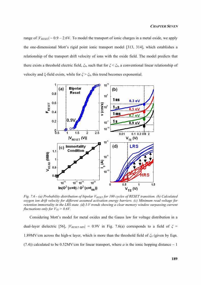
CHAPTER SEVEN
189
range of |VRESET| ~ 0.9 – 2.6V. To model the transport of ionic charges in a metal oxide, we apply
the one-dimensional Mott’s rigid point ionic transport model [313, 314], which establishes a
relationship of the transport drift velocity of ions with the oxide field. The model predicts that
there exists a threshold electric field, ξ0, such that for ξ < ξ0, a conventional linear relationship of
velocity and ξ-field exists, while for ξ > ξ0, this trend becomes exponential.
Fig. 7.6 - (a) Probability distribution of bipolar VRESET for 100 cycles of RESET transition. (b) Calculated oxygen ion drift velocity for different assumed activation energy barriers. (c) Minimum read voltage for retention immortality in the LRS state. (d) I-V trends showing a clear memory window surpassing current fluctuations only for VTE > 0.6V.
Considering Mott’s model for metal oxides and the Gauss law for voltage distribution in a
dual-layer dielectric [56], |VRESET-MIN| = 0.9V in Fig. 7.6(a) corresponds to a field of ξ =
1.89MV/cm across the high-κ layer, which is more than the threshold field of ξ0 (given by Eqn.
(7.4)) calculated to be 0.52MV/cm for linear transport, where a is the ionic hopping distance ~ 1
CHAPTER SEVEN
190
nm [315], q is the electronic charge and kB represents the Boltzmann constant. The condition ξ >
ξ0 implies that RESET occurs in the non-linear high-field ionic transport regime. Fig. 7.6(b) plots
the ionic drift velocity (ν) as a function of the applied voltage for various arbitrarily chosen
diffusive activation energies (∆Hdiff), based on Eqn. (7.5) [315]. The switching time (τ = ν/tHK)
corresponding to ν is also labeled in Fig. 7.6(b). Our voltage sweep for RESET involves a very
slow ramp ~ 0.01-0.02V/s and stress duration at every voltage step is ~ 1 sec.
aqTkB
⋅= 20ξ (7.4)
⎟⎟⎠
⎞⎜⎜⎝
⎛⋅⎟⎟⎠
⎞⎜⎜⎝
⎛ ∆−⋅⋅=
Tkqasinh
TkH
expfavBB
diff
2ξ
(7.5)
Considering a case of |VRESET| = 0.8V < |VRESET-MIN| when no RESET is observed in our
electrical tests, if ∆Hdiff = (0.3, 0.5, 0.7)eV, RESET should have been observed within a short
span of τ ~ (1ns, 1µs, 1ms) respectively, which is well within the 1 sec stress duration at 0.8V.
However, since we do not observe any switching in these cases, it is clear that ∆Hdiff > 0.7eV. By
proof of contradiction, we can therefore imply that ∆Hdiff > 0.7eV. This high activation energy
could be attributed either to the existence of a metal electrode - dielectric interfacial barrier for
O2- transport or the amorphous microstructure of HfSiON. It is therefore necessary to explore
different electrode materials in RRAM design with lower barrier and modify the microstructure
of high-κ materials to be polycrystalline which provides for lower ∆Hdiff ~ 0.57eV [74], so that
switching speed is high and VRESET is kept sufficiently low.
The retention lifetime in the LRS state is affected by drift and diffusion driving forces
experienced by the gettered O2- ions in the top electrode. We can derive an “immortality”
condition for prolonged retention by balancing the diffusion and drift fluxes (which are directed
against each other for positive VREAD), as described by Eqn. (7.6), where D and µ are diffusivity
CHAPTER SEVEN
191
and mobility respectively. Making use of the Nernst-Einstein relationship for low-field and the
Gauss law, the final expression after integration can be expressed by Eqn. (7.7), which quantifies
the minimum VREAD to be applied to achieve net zero flux of O2- ions resulting in “theoretically
infinite” retention. In Eqn. (7.7), x = 0 refers to the TE-HK interface. Fig. 7.6(c) plots the
expected VREAD-MIN based on Eqn. (7.7). We chose a wide range for O2- concentration ratio
considering that equilibrium value of [VO] or [O2-] can range from 1018-1021 cm-3 [316]. As a
conservative estimate, applying VREAD ~ 1.1V can give excellent retention.
[ ] [ ] 022
=⋅−∂
∂⋅−=+ −
−
Ox
ODJJ driftdiff µξ (7.6)
⎟⎟⎠
⎞⎜⎜⎝
⎛+⋅⎟
⎟⎠
⎞⎜⎜⎝
⎛⋅=
=−
=−
−HKSiO
SiOHK
tx
xBMINREAD t
t]O[]O[ln
qTkV
x
x
HKκκ
12 2
02
(7.7)
Very low VREAD in both LRS and HRS states can result in narrow memory windows and
erroneous reading of the memory state as illustrated in Fig. 7.6(d). This is more so the case for
SBD in ultra-thin dielectric based RRAM. The reason behind this observation is that at very low
values of VREAD, the percolated traps in the dielectric may not be accessible by the electron
charge carriers [317] due to the difference in the silicon conduction band energy and the trap’s
energy depth relative to oxide conduction band. Therefore, the leakage current even after SBD
may only be due to the DT / FN tunneling mechanism which is equivalent to the leakage of a
recovered (post-RESET) device in the HRS state. Hence, choosing very low VREAD for V0 mode
operation is not recommended.
Based on the HRS and LRS analysis in this work, use of VREAD ~ 0.8-1.2V ensures very good
retention lifetime in both states. Although this is much higher than 0.1-0.5V used in most studies,
the need for higher VREAD has been justified and this is all the more critical for ultra thin ultra-low
power oxides in future RRAM nodes where SBD is the likely state of the percolated dielectric.
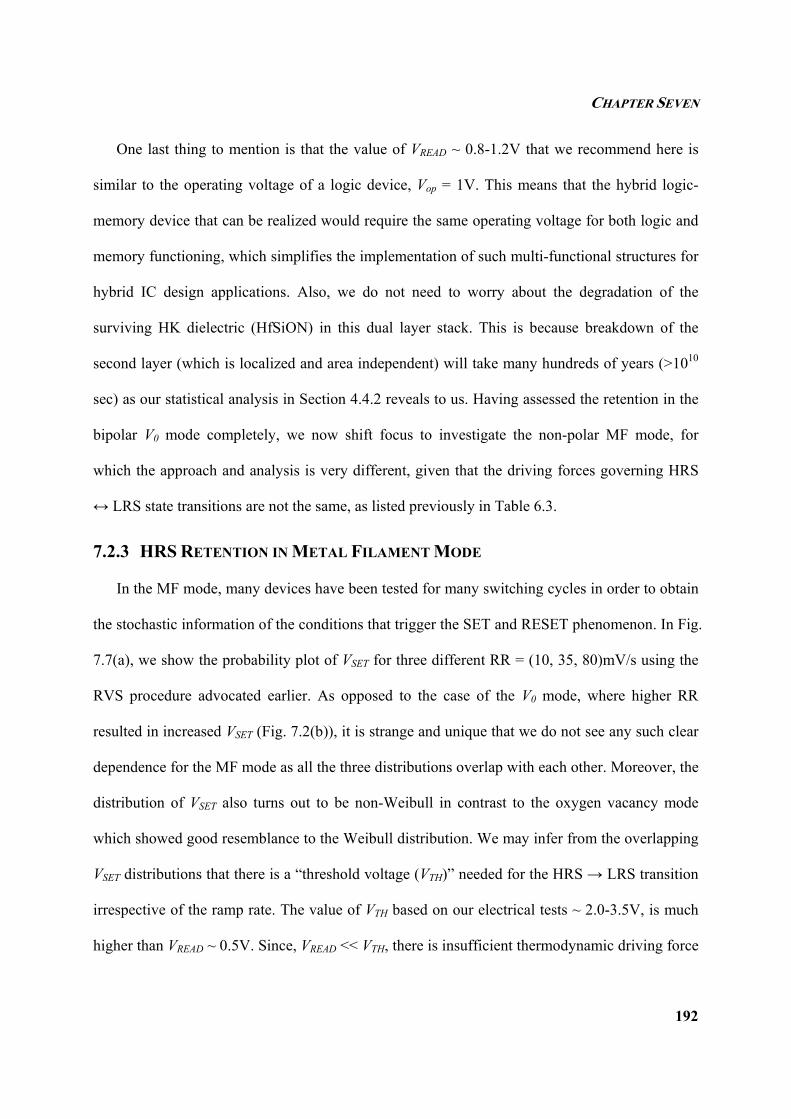
CHAPTER SEVEN
192
One last thing to mention is that the value of VREAD ~ 0.8-1.2V that we recommend here is
similar to the operating voltage of a logic device, Vop = 1V. This means that the hybrid logic-
memory device that can be realized would require the same operating voltage for both logic and
memory functioning, which simplifies the implementation of such multi-functional structures for
hybrid IC design applications. Also, we do not need to worry about the degradation of the
surviving HK dielectric (HfSiON) in this dual layer stack. This is because breakdown of the
second layer (which is localized and area independent) will take many hundreds of years (>1010
sec) as our statistical analysis in Section 4.4.2 reveals to us. Having assessed the retention in the
bipolar V0 mode completely, we now shift focus to investigate the non-polar MF mode, for
which the approach and analysis is very different, given that the driving forces governing HRS
↔ LRS state transitions are not the same, as listed previously in Table 6.3.
7.2.3 HRS RETENTION IN METAL FILAMENT MODE
In the MF mode, many devices have been tested for many switching cycles in order to obtain
the stochastic information of the conditions that trigger the SET and RESET phenomenon. In Fig.
7.7(a), we show the probability plot of VSET for three different RR = (10, 35, 80)mV/s using the
RVS procedure advocated earlier. As opposed to the case of the V0 mode, where higher RR
resulted in increased VSET (Fig. 7.2(b)), it is strange and unique that we do not see any such clear
dependence for the MF mode as all the three distributions overlap with each other. Moreover, the
distribution of VSET also turns out to be non-Weibull in contrast to the oxygen vacancy mode
which showed good resemblance to the Weibull distribution. We may infer from the overlapping
VSET distributions that there is a “threshold voltage (VTH)” needed for the HRS → LRS transition
irrespective of the ramp rate. The value of VTH based on our electrical tests ~ 2.0-3.5V, is much
higher than VREAD ~ 0.5V. Since, VREAD << VTH, there is insufficient thermodynamic driving force
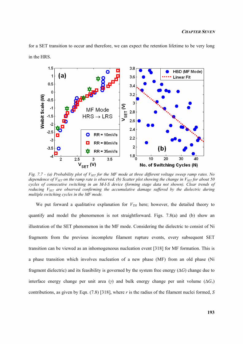
CHAPTER SEVEN
193
for a SET transition to occur and therefore, we can expect the retention lifetime to be very long
in the HRS.
Fig. 7.7 - (a) Probability plot of VSET for the MF mode at three different voltage sweep ramp rates. No dependence of VSET on the ramp rate is observed. (b) Scatter plot showing the change in VSET for about 50 cycles of consecutive switching in an M-I-S device (forming stage data not shown). Clear trends of reducing VSET are observed confirming the accumulative damage suffered by the dielectric during multiple switching cycles in the MF mode.
We put forward a qualitative explanation for VTH here; however, the detailed theory to
quantify and model the phenomenon is not straightforward. Figs. 7.8(a) and (b) show an
illustration of the SET phenomenon in the MF mode. Considering the dielectric to consist of Ni
fragments from the previous incomplete filament rupture events, every subsequent SET
transition can be viewed as an inhomogeneous nucleation event [318] for MF formation. This is
a phase transition which involves nucleation of a new phase (MF) from an old phase (Ni
fragment dielectric) and its feasibility is governed by the system free energy (∆G) change due to
interface energy change per unit area (γ) and bulk energy change per unit volume (∆Gv)
contributions, as given by Eqn. (7.8) [318], where r is the radius of the filament nuclei formed, S
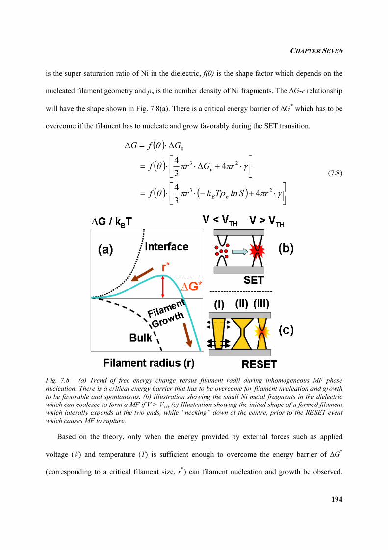
CHAPTER SEVEN
194
is the super-saturation ratio of Ni in the dielectric, f(θ) is the shape factor which depends on the
nucleated filament geometry and ρn is the number density of Ni fragments. The ∆G-r relationship
will have the shape shown in Fig. 7.8(a). There is a critical energy barrier of ∆G* which has to be
overcome if the filament has to nucleate and grow favorably during the SET transition.
( )
( )
( ) ( ) ⎥⎦⎤
⎢⎣⎡ ⋅+−⋅⋅=
⎥⎦⎤
⎢⎣⎡ ⋅+∆⋅⋅=
∆⋅=∆
γπρπθ
γππθ
θ
23
23
0
434
434
rSlnTkrf
rGrf
GfG
nB
v (7.8)
Fig. 7.8 - (a) Trend of free energy change versus filament radii during inhomogeneous MF phase nucleation. There is a critical energy barrier that has to be overcome for filament nucleation and growth to be favorable and spontaneous. (b) Illustration showing the small Ni metal fragments in the dielectric which can coalesce to form a MF if V > VTH.(c) Illustration showing the initial shape of a formed filament, which laterally expands at the two ends, while “necking” down at the centre, prior to the RESET event which causes MF to rupture.
Based on the theory, only when the energy provided by external forces such as applied
voltage (V) and temperature (T) is sufficient enough to overcome the energy barrier of ∆G*
(corresponding to a critical filament size, r*) can filament nucleation and growth be observed.
CHAPTER SEVEN
195
We do not analyze this theory in any further detail here as there are many parameters in the
model that require in-depth studies of their own. However, at least from a qualitative standpoint,
it is clear that a minimum threshold energy (corresponding to VTH) is needed for MF nucleation,
which is why we observed all the VSET distributions to overlap irrespective of the ramp rates
(refer to Fig. 7.7(a)). As long as VREAD << VTH ~ 2.0-3.5V, it can be concluded that HRS retention
is very good in the MF mode.
In Fig. 7.7(b), we plot the value of VSET for ~ 50 consecutive cycles of switching in a
particular device for the MF mode. Although the values of VSET shift up and down in the scatter
plot, there is a general trend of reduction in the VSET value from 3.4V → 2.0V (indicative of
pseudo-random filament nucleation as presented in Chapter 6). This is due to increasing number
or density of incompletely ruptured Ni fragments residing in the dielectric matrix after many
RESET transitions. As the dielectric undergoes cumulative damage with increasing “metallic Ni”
defect centers, the energy barrier (∆G*) for subsequent filament nucleation events is reduced.
Fig. 7.9 - (a) Probability plot of VRESET for two different ramp rates (RR) showing a direct correlation between the two quantities. (b) Resistance evolution with slowly ramped Vg in the LRS state of the MF mode, up to the instant of sudden filament rupture. The complete rupture process can be split into three different stages.
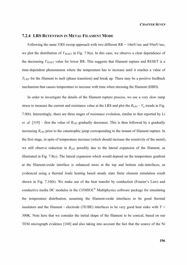
CHAPTER SEVEN
196
7.2.4 LRS RETENTION IN METAL FILAMENT MODE
Following the same VRS sweep approach with two different RR = 14mV/sec and 95mV/sec,
we plot the distribution of VRESET in Fig. 7.9(a). In this case, we observe a clear dependence of
the decreasing VRESET value for lower RR. This suggests that filament rupture and RESET is a
time-dependent phenomenon where the temperature has to increase until it reaches a value of
TCRIT for the filament to melt (phase transition) and break up. There may be a positive feedback
mechanism that causes temperature to increase with time when stressing the filament (HBD).
In order to investigate the details of the filament rupture process, we use a very slow ramp
stress to measure the current and resistance value at the LRS and plot the RLRS – Vg trends in Fig.
7.9(b). Interestingly, there are three stages of resistance evolution, similar to that reported by Li
et. al. [319] – first the value of RLRS gradually decreases. This is then followed by a gradually
increasing RLRS prior to the catastrophic jump corresponding to the instant of filament rupture. In
the first stage, in spite of temperature increase (which should increase the resistivity of the metal),
we still observe reduction in RLRS possibly due to the lateral expansion of the filament, as
illustrated in Fig. 7.8(c). The lateral expansion which would depend on the temperature gradient
at the filament-oxide interface is enhanced more at the top and bottom side-interfaces, as
evidenced using a thermal Joule heating based steady state finite element simulation result
shown in Fig. 7.10(b). We make use of the heat transfer by conduction (Fourier’s Law) and
conductive media DC modules in the COMSOL® Multiphysics software package for simulating
the temperature distribution, assuming the filament-oxide interfaces to be good thermal
insulators and the filament - electrode (TE/BE) interfaces to be very good heat sinks with T =
300K. Note here that we consider the initial shape of the filament to be conical, based on our
TEM micrograph evidence [168] and also taking into account the fact that the source of the Ni
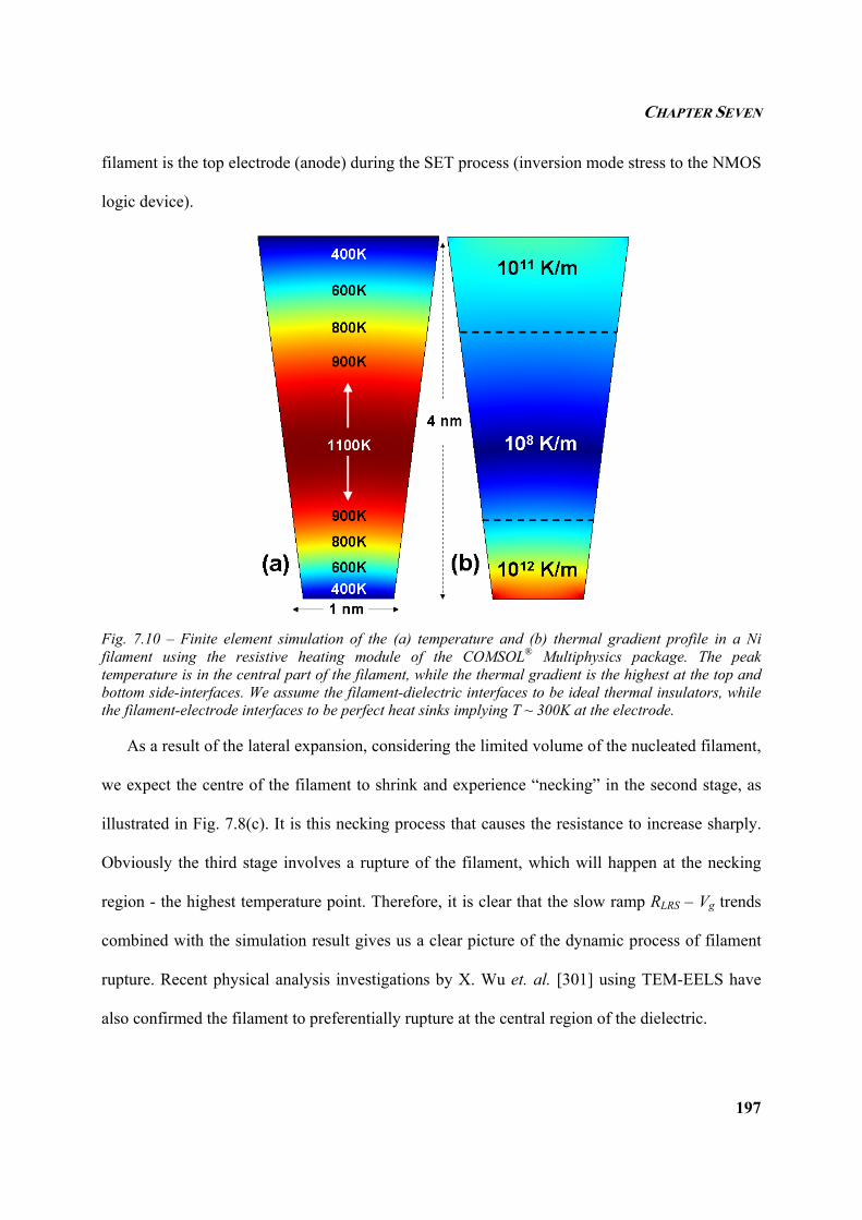
CHAPTER SEVEN
197
filament is the top electrode (anode) during the SET process (inversion mode stress to the NMOS
logic device).
Fig. 7.10 – Finite element simulation of the (a) temperature and (b) thermal gradient profile in a Ni filament using the resistive heating module of the COMSOL® Multiphysics package. The peak temperature is in the central part of the filament, while the thermal gradient is the highest at the top and bottom side-interfaces. We assume the filament-dielectric interfaces to be ideal thermal insulators, while the filament-electrode interfaces to be perfect heat sinks implying T ~ 300K at the electrode.
As a result of the lateral expansion, considering the limited volume of the nucleated filament,
we expect the centre of the filament to shrink and experience “necking” in the second stage, as
illustrated in Fig. 7.8(c). It is this necking process that causes the resistance to increase sharply.
Obviously the third stage involves a rupture of the filament, which will happen at the necking
region - the highest temperature point. Therefore, it is clear that the slow ramp RLRS – Vg trends
combined with the simulation result gives us a clear picture of the dynamic process of filament
rupture. Recent physical analysis investigations by X. Wu et. al. [301] using TEM-EELS have
also confirmed the filament to preferentially rupture at the central region of the dielectric.
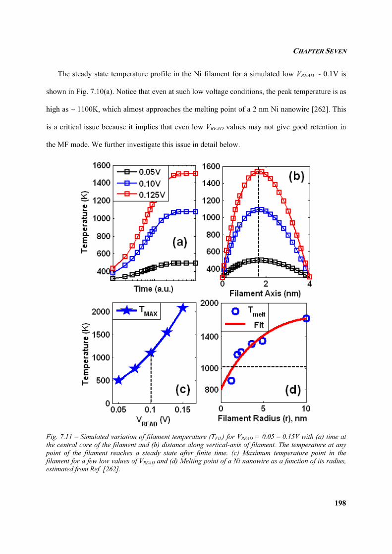
CHAPTER SEVEN
198
The steady state temperature profile in the Ni filament for a simulated low VREAD ~ 0.1V is
shown in Fig. 7.10(a). Notice that even at such low voltage conditions, the peak temperature is as
high as ~ 1100K, which almost approaches the melting point of a 2 nm Ni nanowire [262]. This
is a critical issue because it implies that even low VREAD values may not give good retention in
the MF mode. We further investigate this issue in detail below.
Fig. 7.11 – Simulated variation of filament temperature (TFIL) for VREAD = 0.05 – 0.15V with (a) time at the central core of the filament and (b) distance along vertical-axis of filament. The temperature at any point of the filament reaches a steady state after finite time. (c) Maximum temperature point in the filament for a few low values of VREAD and (d) Melting point of a Ni nanowire as a function of its radius, estimated from Ref. [262].
CHAPTER SEVEN
199
We use the simulation model above to plot the time evolution of peak temperature in the
central core of the filament for VREAD ~ (0.05, 0.10, 0.125)V as plotted in Fig. 7.11(a). After an
ultra-fast transient increase in temperature, a steady state value is reached. The temperature
profile along the vertical axis of the filament is also plotted in Fig. 7.11(b). As expected, we
observed a parabolic trend with the centre having the highest temperature while the ends of the
filament in contact with the electrode functioning as effective sinks with T ~ 300K.
The saturating temperature is plotted versus VREAD in Fig. 7.11(c). This is the most critical
result of this simulation exercise as it shows the peak temperature corresponding to different
VREAD values. It is critical to note that even low VREAD value of 0.1V is sufficient enough to cause
the temperature to go up to 1100-1200K. Considering the lower melting point for thinner Ni
filaments, as plotted in Fig. 7.11(d) [262], for the 2 nm filaments (TMELT ~ 1100K) we have
observed using TEM analysis, even VREAD ~ 0.1V may be sufficient to cause the filament to melt
(rupture). As a result, we infer that retention lifetime in the LRS for MF mode can be very short
and further device design and optimization is needed to address this issue. While the tendency of
Ni to form ultra-thin filaments is useful for achieving RESET, it is detrimental to the retention
lifetime. For the case studied here, we recommend the use of a much lower VREAD ~ 0.05-0.08V
in order to ensure TFIL < TMELT at steady state.
Based on all the detailed analyses presented in this section, it is clear that retention in the
HRS and LRS states for the V0 and MF modes have to be separately studied, as the driving forces
for retention failure are very different in each case. In our investigations here, different values of
VREAD are recommended to achieve prolonged retention in different modes and resistive states of
switching. In the next section, we briefly look into the endurance phenomenon for the V0 and MF
modes. Though we do not see very good endurance in both the modes considering that our gate
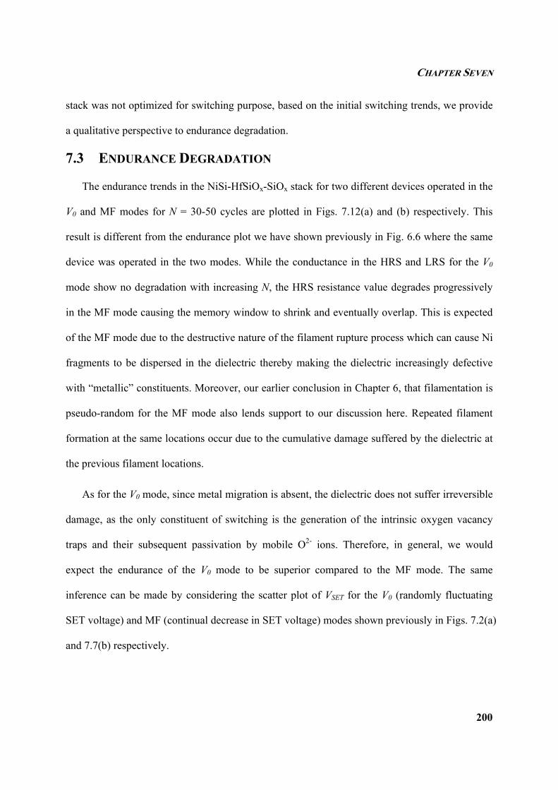
CHAPTER SEVEN
200
stack was not optimized for switching purpose, based on the initial switching trends, we provide
a qualitative perspective to endurance degradation.
7.3 ENDURANCE DEGRADATION
The endurance trends in the NiSi-HfSiOx-SiOx stack for two different devices operated in the
V0 and MF modes for N = 30-50 cycles are plotted in Figs. 7.12(a) and (b) respectively. This
result is different from the endurance plot we have shown previously in Fig. 6.6 where the same
device was operated in the two modes. While the conductance in the HRS and LRS for the V0
mode show no degradation with increasing N, the HRS resistance value degrades progressively
in the MF mode causing the memory window to shrink and eventually overlap. This is expected
of the MF mode due to the destructive nature of the filament rupture process which can cause Ni
fragments to be dispersed in the dielectric thereby making the dielectric increasingly defective
with “metallic” constituents. Moreover, our earlier conclusion in Chapter 6, that filamentation is
pseudo-random for the MF mode also lends support to our discussion here. Repeated filament
formation at the same locations occur due to the cumulative damage suffered by the dielectric at
the previous filament locations.
As for the V0 mode, since metal migration is absent, the dielectric does not suffer irreversible
damage, as the only constituent of switching is the generation of the intrinsic oxygen vacancy
traps and their subsequent passivation by mobile O2- ions. Therefore, in general, we would
expect the endurance of the V0 mode to be superior compared to the MF mode. The same
inference can be made by considering the scatter plot of VSET for the V0 (randomly fluctuating
SET voltage) and MF (continual decrease in SET voltage) modes shown previously in Figs. 7.2(a)
and 7.7(b) respectively.
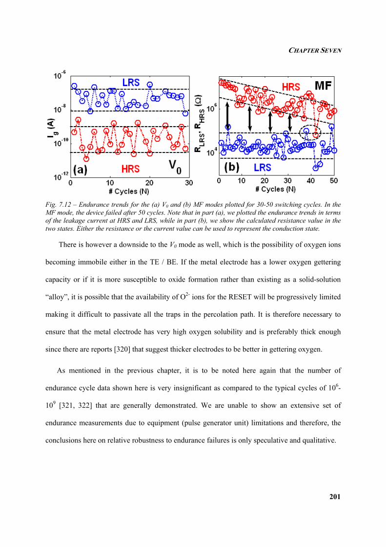
CHAPTER SEVEN
201
Fig. 7.12 – Endurance trends for the (a) V0 and (b) MF modes plotted for 30-50 switching cycles. In the MF mode, the device failed after 50 cycles. Note that in part (a), we plotted the endurance trends in terms of the leakage current at HRS and LRS, while in part (b), we show the calculated resistance value in the two states. Either the resistance or the current value can be used to represent the conduction state.
There is however a downside to the V0 mode as well, which is the possibility of oxygen ions
becoming immobile either in the TE / BE. If the metal electrode has a lower oxygen gettering
capacity or if it is more susceptible to oxide formation rather than existing as a solid-solution
“alloy”, it is possible that the availability of O2- ions for the RESET will be progressively limited
making it difficult to passivate all the traps in the percolation path. It is therefore necessary to
ensure that the metal electrode has very high oxygen solubility and is preferably thick enough
since there are reports [320] that suggest thicker electrodes to be better in gettering oxygen.
As mentioned in the previous chapter, it is to be noted here again that the number of
endurance cycle data shown here is very insignificant as compared to the typical cycles of 106-
109 [321, 322] that are generally demonstrated. We are unable to show an extensive set of
endurance measurements due to equipment (pulse generator unit) limitations and therefore, the
conclusions here on relative robustness to endurance failures is only speculative and qualitative.
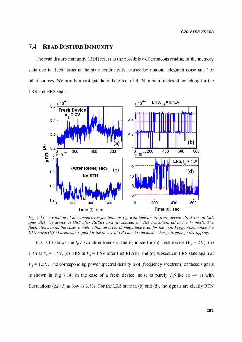
CHAPTER SEVEN
202
7.4 READ DISTURB IMMUNITY
The read disturb immunity (RDI) refers to the possibility of erroneous reading of the memory
state due to fluctuations in the state conductivity, caused by random telegraph noise and / or
other sources. We briefly investigate here the effect of RTN in both modes of switching for the
LRS and HRS states.
Fig. 7.13 – Evolution of the conductivity fluctuations (Ig) with time for (a) fresh device, (b) device at LRS after SET, (c) device at HRS after RESET and (d) subsequent SET transition, all in the V0 mode. The fluctuations in all the cases is well within an order of magnitude even for the high VREAD. Also, notice the RTN noise (1/f2) Lorentzian signal for the device at LRS due to stochastic charge trapping / detrapping.
Fig. 7.13 shows the Ig-t evolution trends in the V0 mode for (a) fresh device (Vg = 2V), (b)
LRS at Vg = 1.5V, (c) HRS at Vg = 1.5V after first RESET and (d) subsequent LRS state again at
Vg = 1.5V. The corresponding power spectral density plot (frequency spectrum) of these signals
is shown in Fig 7.14. In the case of a fresh device, noise is purely 1/f-like (α → 1) with
fluctuations (∆I / I) as low as 3.8%. For the LRS state in (b) and (d), the signals are clearly RTN
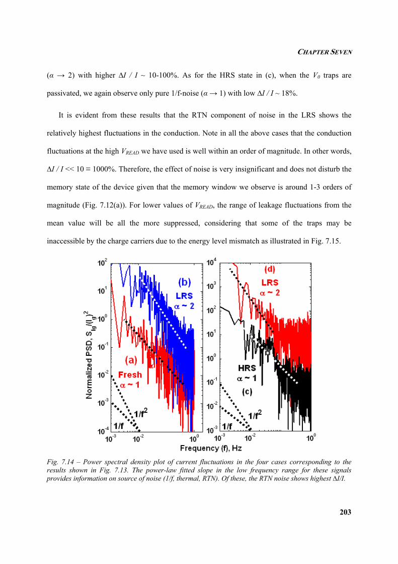
CHAPTER SEVEN
203
(α → 2) with higher ∆I / I ~ 10-100%. As for the HRS state in (c), when the V0 traps are
passivated, we again observe only pure 1/f-noise (α → 1) with low ∆I / I ~ 18%.
It is evident from these results that the RTN component of noise in the LRS shows the
relatively highest fluctuations in the conduction. Note in all the above cases that the conduction
fluctuations at the high VREAD we have used is well within an order of magnitude. In other words,
∆I / I << 10 ≡ 1000%. Therefore, the effect of noise is very insignificant and does not disturb the
memory state of the device given that the memory window we observe is around 1-3 orders of
magnitude (Fig. 7.12(a)). For lower values of VREAD, the range of leakage fluctuations from the
mean value will be all the more suppressed, considering that some of the traps may be
inaccessible by the charge carriers due to the energy level mismatch as illustrated in Fig. 7.15.
Fig. 7.14 – Power spectral density plot of current fluctuations in the four cases corresponding to the results shown in Fig. 7.13. The power-law fitted slope in the low frequency range for these signals provides information on source of noise (1/f, thermal, RTN). Of these, the RTN noise shows highest ∆I/I.
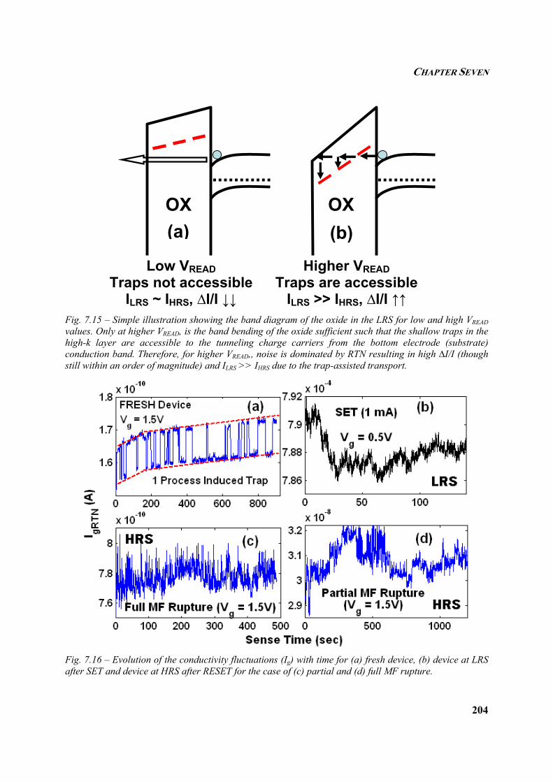
CHAPTER SEVEN
204
Fig. 7.15 – Simple illustration showing the band diagram of the oxide in the LRS for low and high VREAD values. Only at higher VREAD, is the band bending of the oxide sufficient such that the shallow traps in the high-k layer are accessible to the tunneling charge carriers from the bottom electrode (substrate) conduction band. Therefore, for higher VREAD,, noise is dominated by RTN resulting in high ∆I/I (though still within an order of magnitude) and ILRS >> IHRS due to the trap-assisted transport.
Fig. 7.16 – Evolution of the conductivity fluctuations (Ig) with time for (a) fresh device, (b) device at LRS after SET and device at HRS after RESET for the case of (c) partial and (d) full MF rupture.
Low VREAD Traps not accessible
ILRS ~ IHRS, ∆I/I ↓↓
Higher VREAD Traps are accessible
ILRS >> IHRS, ∆I/I ↑↑
(a) (b) OX OX
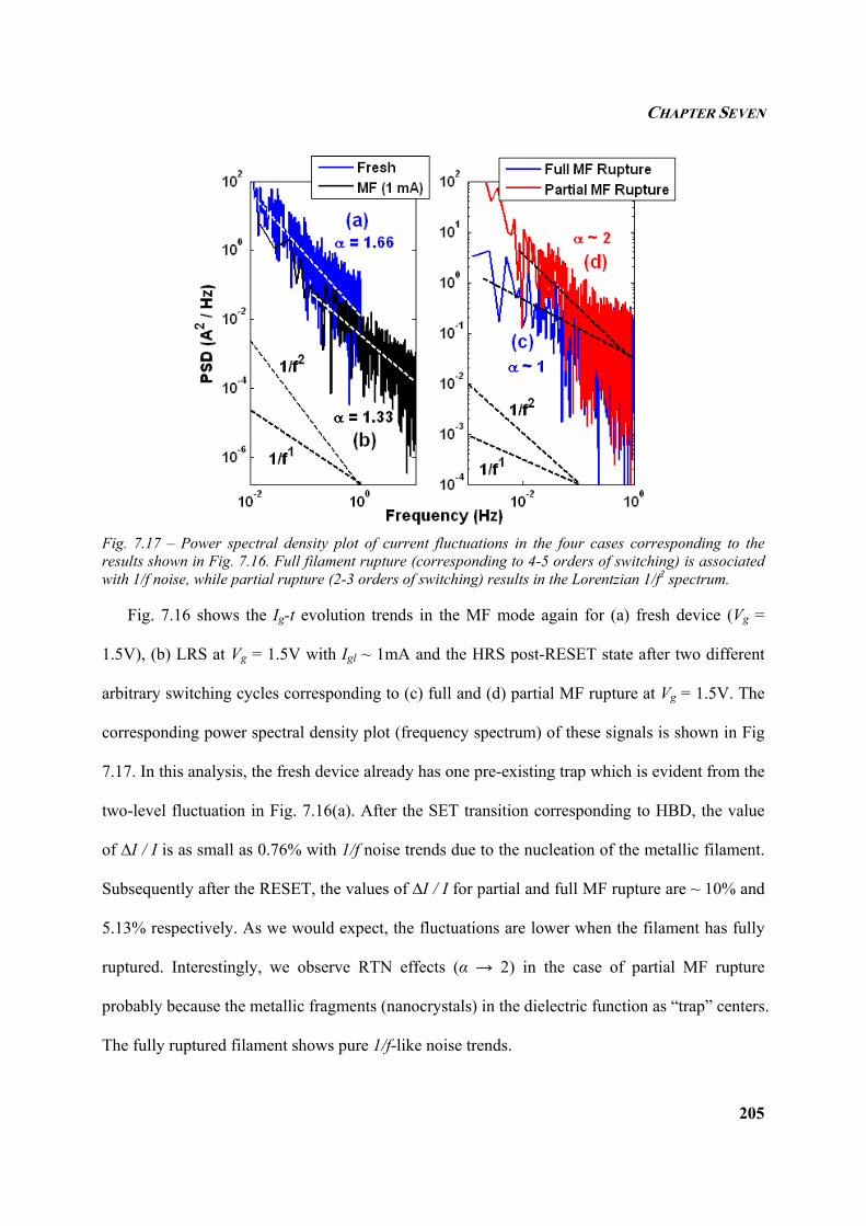
CHAPTER SEVEN
205
Fig. 7.17 – Power spectral density plot of current fluctuations in the four cases corresponding to the results shown in Fig. 7.16. Full filament rupture (corresponding to 4-5 orders of switching) is associated with 1/f noise, while partial rupture (2-3 orders of switching) results in the Lorentzian 1/f2 spectrum.
Fig. 7.16 shows the Ig-t evolution trends in the MF mode again for (a) fresh device (Vg =
1.5V), (b) LRS at Vg = 1.5V with Igl ~ 1mA and the HRS post-RESET state after two different
arbitrary switching cycles corresponding to (c) full and (d) partial MF rupture at Vg = 1.5V. The
corresponding power spectral density plot (frequency spectrum) of these signals is shown in Fig
7.17. In this analysis, the fresh device already has one pre-existing trap which is evident from the
two-level fluctuation in Fig. 7.16(a). After the SET transition corresponding to HBD, the value
of ∆I / I is as small as 0.76% with 1/f noise trends due to the nucleation of the metallic filament.
Subsequently after the RESET, the values of ∆I / I for partial and full MF rupture are ~ 10% and
5.13% respectively. As we would expect, the fluctuations are lower when the filament has fully
ruptured. Interestingly, we observe RTN effects (α → 2) in the case of partial MF rupture
probably because the metallic fragments (nanocrystals) in the dielectric function as “trap” centers.
The fully ruptured filament shows pure 1/f-like noise trends.
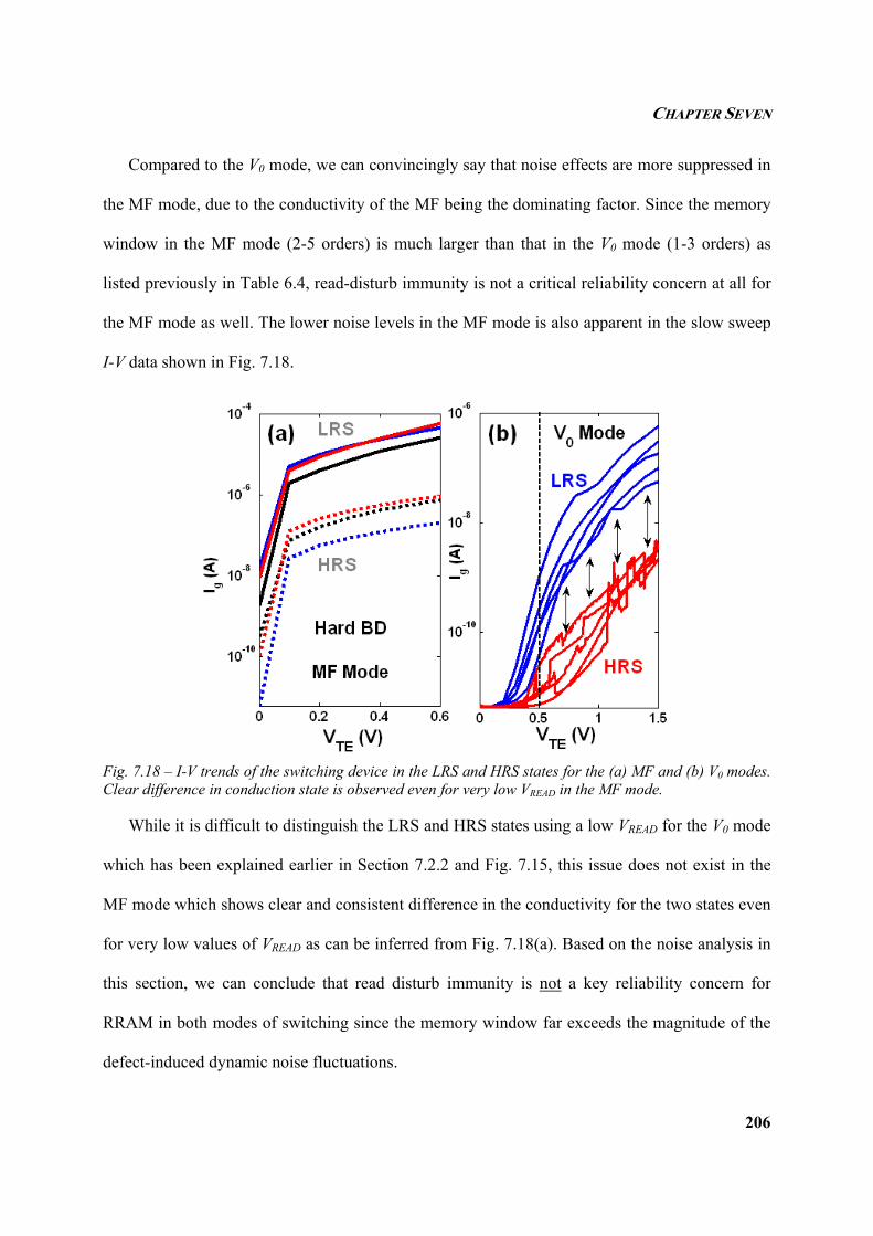
CHAPTER SEVEN
206
Compared to the V0 mode, we can convincingly say that noise effects are more suppressed in
the MF mode, due to the conductivity of the MF being the dominating factor. Since the memory
window in the MF mode (2-5 orders) is much larger than that in the V0 mode (1-3 orders) as
listed previously in Table 6.4, read-disturb immunity is not a critical reliability concern at all for
the MF mode as well. The lower noise levels in the MF mode is also apparent in the slow sweep
I-V data shown in Fig. 7.18.
Fig. 7.18 – I-V trends of the switching device in the LRS and HRS states for the (a) MF and (b) V0 modes. Clear difference in conduction state is observed even for very low VREAD in the MF mode.
While it is difficult to distinguish the LRS and HRS states using a low VREAD for the V0 mode
which has been explained earlier in Section 7.2.2 and Fig. 7.15, this issue does not exist in the
MF mode which shows clear and consistent difference in the conductivity for the two states even
for very low values of VREAD as can be inferred from Fig. 7.18(a). Based on the noise analysis in
this section, we can conclude that read disturb immunity is not a key reliability concern for
RRAM in both modes of switching since the memory window far exceeds the magnitude of the
defect-induced dynamic noise fluctuations.
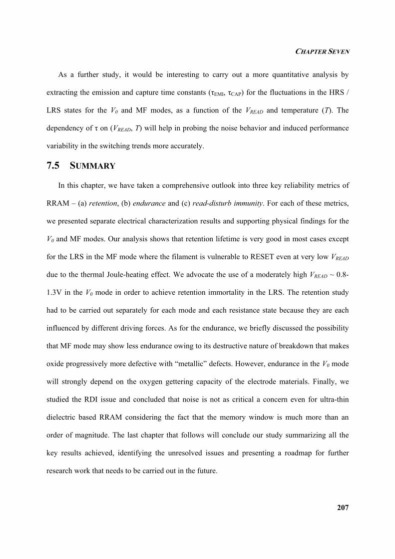
CHAPTER SEVEN
207
As a further study, it would be interesting to carry out a more quantitative analysis by
extracting the emission and capture time constants (τEMI, τCAP) for the fluctuations in the HRS /
LRS states for the V0 and MF modes, as a function of the VREAD and temperature (T). The
dependency of τ on (VREAD, T) will help in probing the noise behavior and induced performance
variability in the switching trends more accurately.
7.5 SUMMARY
In this chapter, we have taken a comprehensive outlook into three key reliability metrics of
RRAM – (a) retention, (b) endurance and (c) read-disturb immunity. For each of these metrics,
we presented separate electrical characterization results and supporting physical findings for the
V0 and MF modes. Our analysis shows that retention lifetime is very good in most cases except
for the LRS in the MF mode where the filament is vulnerable to RESET even at very low VREAD
due to the thermal Joule-heating effect. We advocate the use of a moderately high VREAD ~ 0.8-
1.3V in the V0 mode in order to achieve retention immortality in the LRS. The retention study
had to be carried out separately for each mode and each resistance state because they are each
influenced by different driving forces. As for the endurance, we briefly discussed the possibility
that MF mode may show less endurance owing to its destructive nature of breakdown that makes
oxide progressively more defective with “metallic” defects. However, endurance in the V0 mode
will strongly depend on the oxygen gettering capacity of the electrode materials. Finally, we
studied the RDI issue and concluded that noise is not as critical a concern even for ultra-thin
dielectric based RRAM considering the fact that the memory window is much more than an
order of magnitude. The last chapter that follows will conclude our study summarizing all the
key results achieved, identifying the unresolved issues and presenting a roadmap for further
research work that needs to be carried out in the future.
CHAPTER EIGHT
208
CHAPTER EIGHT
CCCOOONNNCCCLLLUUUSSSIIIOOONNN AAANNNDDD RRREEECCCOOOMMMMMMEEENNNDDDAAATTTIIIOOONNNSSS
In this concluding chapter, we shall first list out the various key results and implications of
the study focusing on logic device reliability as well as resistive switching memory. This will be
followed by some recommendations for further work to be carried out in these areas in order to
gain in-depth understanding and assess the feasibility of implementation of high-κ based thin
films for sub 22nm CMOS logic and sub 10nm non-volatile memory device technology nodes.
8.1 SUMMARY OF RESULTS ACHIEVED
8.1.1 LOGIC DEVICE RELIABILITY
In a dual layer dielectric stack, IL is always the first layer to breakdown for all voltage
stress conditions (for both operating and accelerated stress cases) and thickness
combinations of HfO2 and SiOx. This sequence of breakdown is universal for the case of
substrate injection tests that we have carried out on NMOS devices.
Circuit level failure of HK-IL gate stack can only occur by multiple IL SBD events. It is
not feasible for a complete HK-IL stack breakdown to occur for Vop = 1V.
Grain boundaries are defective regions with higher localized trap generation rate that can
be a few orders of magnitude more than that in the bulk. It is therefore probable to observe
IL BD events beneath the GB contour regions as the electric field across the IL layer is
higher at the low resistivity GB location.
HK-IL stack failure does not follow Weibull distribution and moreover, even the failure
CHAPTER EIGHT
209
distribution for a pure-HK layer with polycrystalline microstructure is “non-Weibullian”
due to the non-random trap generation.
Zero-IL stacks may be detrimental from a reliability point of view considering that there is
no IL that can act as a buffer and “voltage splitter” to reduce the voltage drop across the
HK layer. As a result, the HK film subjected to full gate stress may tend to undergo SBD at
a much earlier stage. For ZIL stack, the initial leakage current at time zero is also bound to
be high due to the GB fault lines bridging the gate and the substrate.
While area scaling is applicable to the IL BD events, it may not be valid for HK BD in very
small area devices as the trap generation in the HK film is significantly enhanced at the
localized IL SBD spots.
The breakdown in the IL and HK during accelerated stress tend to be highly correlated in
general. However, for very defective HK process with “trappy” GB regions, there is a finite
probability for the BD locations to be uncorrelated.
The oxygen vacancy traps in NMOS devices can be passivated using a bipolar stress
scheme for metal electrode based gate stacks such as NiSi, TiN and TaN. These electrodes
serve as very good oxygen reservoirs and this interesting property can be used to trigger
SBD recovery, thereby rejuvenating device and circuit performance. We propose the idea
of “self-repair” of an integrated circuit by a simple reflash at regular intervals. This
breakdown recovery is not plausible for a PMOS device since the inversion mode (Vg < 0V)
of operation causes O2- ions to be driven towards the Si substrate which is not oxygen
soluble.
In dual-layer stacks, where only multiple IL SBD events are bound to occur, it is
CHAPTER EIGHT
210
energetically not favorable for metal migration and filament formation to occur from the
gate electrode due to low temperature conditions at the percolated region (TPERC < 500K).
As a result, for Vop = 1V, occurrence of HBD is a very rare event and therefore, it is not a
very critical reliability concern. However, it may reappear as a plausible failure mode for
sub-16 nm node ZIL gate stacks considering the presence of high diffusivity GB regions
bridging the gate and substrate.
8.1.2 RESISTIVE SWITCHING MEMORY
The multiple breakdown and recovery cycles of SBD and HBD in MG-HK transistor M-I-S
stacks may be interpreted as a resistive switching phenomenon similar to that observed in
M-I-M capacitor structures for RRAM. A clear analogy can be drawn between “breakdown
versus forming / SET transition” as well as “recovery versus RESET transition”.
Two modes of switching are observed for low (Igl ~ 0.7-2µA) and high (Igl ~ 0.1-1mA)
compliance capped forming / SET transition, corresponding to oxygen vacancy (V0) and
metallic (MF) conductive filaments respectively, as evidenced through a suite of electrical
characterization tests and physical analysis. These two modes of switching are fully
independent (note that the role of V0 in the MF mode is relatively insignificant) and the
driving forces governing the switching mechanisms in the two cases are different. This
interesting observation enables us to realize dual mode switching RRAM which can first be
operated in the V0 mode, followed subsequently by the MF mode. While switching in the
V0 mode is bipolar, the MF regime resistive transitions are polarity independent.
M-I-S stacks are sufficient to realize a resistive memory application and this opens up the
possibility of front-end hybrid logic-memory devices for system-on-chip design wherein
the same transistor can be interchangeably operated either as a logic or a memory device.
CHAPTER EIGHT
211
Front-end RRAM based hybrid circuit design is beneficial in terms of higher integration
density and enhanced thermal budget, as compared to the back-end MIM implementation
scheme.
The transistor structure enables us to probe the location of filament nucleation for multiple
switching cycles. While filament evolution is “fully random” for the V0 mode (depending
on the maximum VRESET applied), it is “pseudo-random” in the MF mode due to the
destructive nature of the process that causes irreversible damage to the dielectric which
comprises increasing density of “metallic” defects with prolonged switching.
From a reliability viewpoint, retention lifetime is very good in all cases except for the LRS
in the MF mode wherein even low VREAD ~ 0.1V is sufficient to cause Joule heating assisted
high thermal stress that approaches the melting point of the narrow Ni filaments causing
vulnerability to unintended rupture. As for endurance, we expect the V0 mode switching to
be better provided the electrode has high oxygen solubility. Finally, for the random
telegraph noise analysis, we conclude that its effect is very minimal (much less than an
order of magnitude) and therefore does not affect the memory state reading process.
8.2 RECOMMENDATIONS FOR FURTHER WORK
8.2.1 UNRESOLVED ISSUES FOR FRONT-END DEVICE RELIABILITY
While it is generally perceived that research concerning MG-HK stack reliability is saturating,
there are many unresolved issues that need to be addressed in order to be able to scale down the
transistors further into the sub-16 nm technology node.
Microstructural Variability – Based on STM analysis, it is known that the grain size in
polycrystalline HK ranges between 20-30 nm [237]. Considering that future logic devices
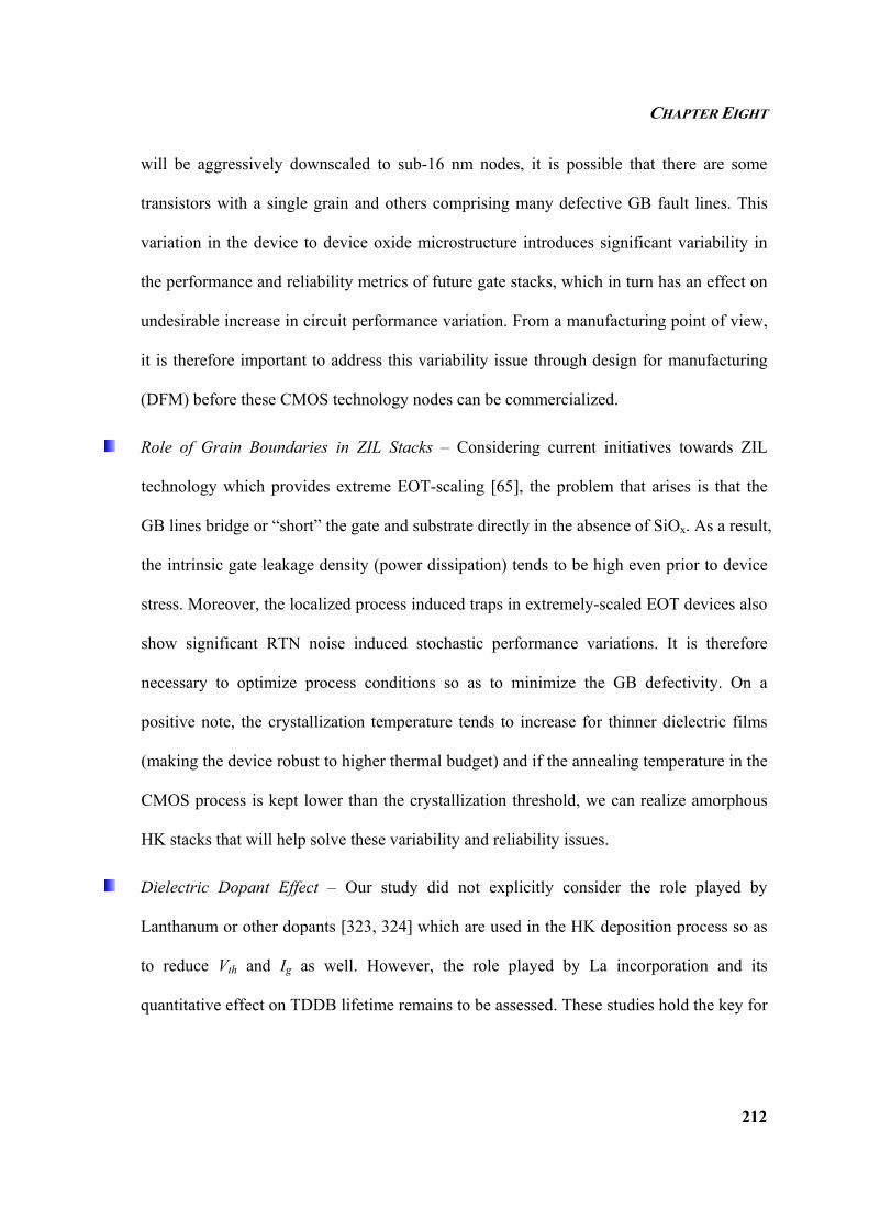
CHAPTER EIGHT
212
will be aggressively downscaled to sub-16 nm nodes, it is possible that there are some
transistors with a single grain and others comprising many defective GB fault lines. This
variation in the device to device oxide microstructure introduces significant variability in
the performance and reliability metrics of future gate stacks, which in turn has an effect on
undesirable increase in circuit performance variation. From a manufacturing point of view,
it is therefore important to address this variability issue through design for manufacturing
(DFM) before these CMOS technology nodes can be commercialized.
Role of Grain Boundaries in ZIL Stacks – Considering current initiatives towards ZIL
technology which provides extreme EOT-scaling [65], the problem that arises is that the
GB lines bridge or “short” the gate and substrate directly in the absence of SiOx. As a result,
the intrinsic gate leakage density (power dissipation) tends to be high even prior to device
stress. Moreover, the localized process induced traps in extremely-scaled EOT devices also
show significant RTN noise induced stochastic performance variations. It is therefore
necessary to optimize process conditions so as to minimize the GB defectivity. On a
positive note, the crystallization temperature tends to increase for thinner dielectric films
(making the device robust to higher thermal budget) and if the annealing temperature in the
CMOS process is kept lower than the crystallization threshold, we can realize amorphous
HK stacks that will help solve these variability and reliability issues.
Dielectric Dopant Effect – Our study did not explicitly consider the role played by
Lanthanum or other dopants [323, 324] which are used in the HK deposition process so as
to reduce Vth and Ig as well. However, the role played by La incorporation and its
quantitative effect on TDDB lifetime remains to be assessed. These studies hold the key for
CHAPTER EIGHT
213
future front-end technology since doping effects are inevitable to achieving good ultra low-
power devices.
NBTI-TDDB Interaction Study – While we focused only on the TDDB study, the NBTI /
PBTI effect is also an important failure mechanism that is being extensively studied. Since
both these failure mechanisms are caused by the presence of bulk and interface traps in the
gate dielectric, it is necessary to understand the correlation of these two failure mechanisms
and how one affects the other [325, 326]. This dependency study is still in its incipient
stages and requires more focus.
Circuit Level Performance Degradation – Dielectric breakdown study is in most cases
confined to the individual device level analysis. The only circuit level implication we
address is the use of the area scaling law for lifetime prediction. However, it is important to
understand and quantify the effect of dielectric SBD / HBD (single / multiple such events)
and its recovery on the degradation / recovery in performance of the ring oscillator circuit
(frequency) [266, 327], the SRAM butterfly curve response (static noise margin) etc…
Such analysis can be carried out either using simulation packages based on circuit models
(SPICE) [328, 329] or by carrying out electrical tests on circuit level test structures.
Design for Reliability – Our studies have opened up the possibility of approaching design
for reliability from a materials perspective wherein we explicitly consider the role of the
electrode material and its oxygen gettering capacity on the recovery of SBD. Such material
design initiatives help in significantly enhancing the TDDB robustness of advanced MG-
HK stacks. Further DFR approaches need to be considered from a process design, circuit
layout design and device architecture design point of view. From a process point of view,
one of the recent proposals include the use of identical multi-layer thin high-κ films [330-
CHAPTER EIGHT
214
332] in ZIL devices. The idea is to say deposit 1 nm (× 2) of HfO2 in a sequence of two
separate ALD steps rather than a single step of 2 nm HfO2. The advantage from this simple
process design alteration is that the GB in the two HK films may be misaligned to each
other and as a result, we avoid the possibility of a direct low resistivity path shorting the
gate and substrate. This reduces gate tunneling current (as process induced traps are no
longer aligned to favor enhanced TAT) and its variability [330] and also increases the
number of traps needed to initiate a percolation BD as illustrated in Fig. 8.1. As for the
device architecture, it is necessary to consider the difference in field distribution and its
effect on oxide BD kinetics for planar transistors versus FinFETs and gate-all-around
(GAA) structures that are touted to be the future of scaled CMOS technology nodes, which
Intel® has already implemented for the 22 nm line. Although there are some initial reports
addressing these topics [333], in-depth analysis is still needed.
Fig. 8.1 – Illustration of a 2 nm polycrystalline HfO2 film deposited by (a) single stage of ALD and (b) two stages of ALD each with 1 nm film thickness. The GB misalignment for the two-layer HK film with the same effective thickness results in improved robustness to TDDB as more traps are needed to initiate a percolation path. The green and red traps refer to process and stress induced ones respectively.
HK on III-V Reliability – While the role of the gate electrode and dielectric has been the
main theme of our study, the role played by the substrate material was not investigated as
our focus has been on Si-based technology. However, considering the need for high
mobility transistors using Ge and III-V materials such as GaAs, InGaAs, and InP, the role
played by the substrate and its interface with the dielectric on the TDDB phenomenon has
to be understood [334]. Given that the HK interface with III-V substrate tends to be
CHAPTER EIGHT
215
defective and also considering that there is no thermodynamically stable intrinsic oxide for
the III-V materials [335], it is expected that the TDDB and NBTI effects for alternate
substrate materials will be more severe. These issues have to be studied from a material,
physical and statistical viewpoint in order to qualify these new substrates for future high-
speed circuit applications.
8.2.2 FURTHER SCOPE FOR RESISTIVE MEMORY STUDY
In the context of the RRAM, our aim was to only understand the switching mechanism and
reliability aspects of memory storage using the M-I-S transistor as the test structure. We did not
focus on improving the performance of the RRAM for state-of-the-art application in comparison
to most studies which report on improvement in parameters such as nanosecond switching speed,
forming-free device realization [304], multi-bit storage operation [297], achieving self-
compliance [160], using transistor as a current limiter in series with the memristor for better
compliance control [336] and so on… There is still more work needed to fully understand
RRAM and qualify it for commercial use.
Better retention models are needed that can accurately forecast the memory state longevity
for various set of conditions including voltage and ambient temperature.
Most models for explaining the RRAM operation still tend to be phenomenological. This is
because the mechanism of switching has been largely speculative, possibly due to the very
wide range of materials (oxides, polymers) and variants of RRAM (such as CBRAM) [337]
being explored that make it hard to nail down one single universal model based on
fundamental physics, as compared to the logic FET, which is so well understood and
accurately modeled. Unified efforts are needed to establish common ground and propose
CHAPTER EIGHT
216
analytical physics-based models for a given class of switching materials – say organic
polymers and inorganic high-κ dielectrics.
Current reports on RRAM performance using M-I-M capacitors tend to show significant
variability in the switching voltage partly due to the nanometer range rough interfaces
between the metal and dielectric. It is important to approach this issue from a design for
variability perspective wherein the key bottlenecks to reducing operational variance are
identified and solved through RRAM circuit / material / process / operation scheme design.
It is apparent from all the above discussions that the concept of “design” for reliability /
manufacturability / variability and its potential to solving many problems for logic and memory
devices holds the key to enabling aggressive downscaling and successful implementation of
future CMOS and NVM technology nodes. Therefore, it is essential to allocate resources in the
academia and the industry focusing on such design initiatives that can help us progress in a
“smarter” and more “cost-effective” way as decisions taken in the design phase tend to account
for 65-70% of the overall locked-in costs for implementing any new technology.
LIST OF PUBLICATIONS
217
LLLIIISSSTTT OOOFFF PPPUUUBBBLLLIIICCCAAATTTIIIOOONNNSSS
FIRST AUTHOR PUBLICATIONS
1. N. Raghavan, K.L. Pey, X. Wu, W.H. Liu and M. Bosman, "Percolative model and thermodynamic analysis of oxygen ion mediated resistive switching", IEEE Electron Device Letters, Vol. 33, No. 5, pp.712-714, (2012).
2. N. Raghavan, K.L. Pey, K. Shubhakar, X. Wu, W.H. Liu and M. Bosman, "Role of grain boundary percolative defects and localized trap generation on the reliability statistics of high-κ gate dielectric stacks", IEEE International Reliability Physics Symposium (IRPS), Anaheim, Orange County, California, 6.A.1.1-6.A.1.11, (2012).
3. N. Raghavan, K.L. Pey, X. Li, W.H. Liu, X. Wu, M. Bosman and T. Kauerauf, “Very low reset current in RRAM achieved in the oxygen vacancy controlled regime”, IEEE Electron Device Letters, Vol. 32, No. 6, pp.716-718, (2011).
4. N. Raghavan, K.L. Pey, W.H. Liu, X. Wu, X. Li and M. Bosman, “Evidence for compliance controlled oxygen vacancy and metal filament based resistive switching mechanisms in RRAM”, 17th International Symposium on Insulating Films on Semiconductors (INFOS), Grenoble, France. Published in Microelectronic Engineering, Vol. 88, Issue 7, pp.1124-1128, (2011).
5. N. Raghavan, W.H. Liu, X. Li, X. Wu, M. Bosman and K.L. Pey, "Filamentation mechanism of resistive switching in fully-silicided high-κ gate stacks", IEEE Electron Device Letters, Vol. 32, No. 4, pp.455-457, (2011).
6. N. Raghavan, K.L. Pey, X. Wu, W.H. Liu, X. Li, M. Bosman and T. Kauerauf, "Oxygen soluble gate electrodes for prolonged high-κ gate stack reliability", IEEE Electron Device Letters, Vol. 32, No. 3, pp.252-254, (2011).
7. N. Raghavan, K.L. Pey, K. Shubhakar and M. Bosman, "Modified percolation model for polycrystalline high-κ gate dielectric stack with grain boundary defects", IEEE Electron Device Letters, Vol. 32, No. 1, pp.78-80, (2011).
8. N. Raghavan, K.L. Pey, W.H. Liu and M. Bosman, "Post breakdown gate current low frequency noise spectrum as a detection tool for high-κ and interfacial layer breakdown", IEEE Electron Device Letters, Vol. 31, No. 9, pp.1035-1037, (2010).
LIST OF PUBLICATIONS
218
9. N. Raghavan, K.L. Pey, W.H. Liu, X. Wu and X. Li, “Unipolar Recovery of Dielectric Breakdown in Fully Silicided high-κ gate stacks and its reliability implications”, Applied Physics Letters, 96, 142901, (2010).
10. N. Raghavan, K.L. Pey, W.H. Liu and X. Li, “New statistical model to decode the reliability and Weibull Slope of High-κ and Interfacial Layer in a Dual Layer Dielectric Stack”, IEEE International Reliability Physics Symposium (IRPS), Anaheim, California, pp.778-786, (2010).
11. N. Raghavan, K.L. Pey and X. Li, “Detection of high-κ and interfacial layer breakdown using the tunneling mechanism in a dual layer dielectric stack”, Applied Physics Letters, Vol. 95, 222903, (2009).
12. N. Raghavan, X. Wu, X. Li, W.H. Liu, V.L. Lo and K.L. Pey, “Post breakdown reliability enhancement of ULSI circuits with novel gate dielectric stacks”, IEEE International Symposium on Integrated Circuits (ISIC), Singapore, pp.505-513, (2009).
CO-AUTHORED PUBLICATIONS
13. K. Shubhakar, K.L. Pey, M. Bosman, R. Thamankar, Z.R. Wang, N. Raghavan, S.S. Kushvaha and S.J. O'Shea, "Nanoscale physical analysis of localized breakdown events in HfO2 based dielectric stacks : A correlation study of STM-induced breakdown with C-AFM and TEM", IEEE International Symposium on the Physical and Failure Analysis of Integrated Circuits (IPFA), Singapore, Accepted, (2012).
14. W.H. Liu, K.L. Pey, N. Raghavan, X. Wu and M. Bosman, "Triggering voltage for post-breakdown random telegraph noise in HfLaO dielectric metal gate metal-oxide-semiconductor field effect transistors and its reliability implications", Journal of Applied Physics, Vol. 111, Issue 2, 024101, (2012).
15. K.L. Pey, N. Raghavan, X. Wu, W.H. Liu, X. Li, M. Bosman, K. Shubhakar, Z.Z. Lwin, Y.N. Chen, H. Qin and T. Kauerauf, "Physical analysis of breakdown in high-κ / metal gate stacks using TEM/EELS and STM for reliability enhancement", 17th International Symposium on Insulating Films on Semiconductors (INFOS), Invited Paper, Grenoble, France. Published in Microelectronic Engineering, Vol. 88, Issue 7, pp.1365-1372, (2011).
16. W.H. Liu, K.L. Pey, X. Wu, N. Raghavan, A. Padovani, L. Larcher, L. Vandelli, M. Bosman and T. Kauerauf, "Threshold shift observed in resistive switching in metal-oxide-semiconductor transistors and the effect of forming gas anneal", Applied Physics Letters, Vol. 99, Issue 23, 232909, (2011).
LIST OF PUBLICATIONS
219
17. X. Wu, K.L. Pey, N. Raghavan, W.H. Liu, X. Li, P. Bai, G. Zhang and M. Bosman, "Using post-breakdown conduction study in MIS structure to better understand resistive switching mechanism in MIM stack", Nanotechnology, Vol. 22, No. 45, 455702, (2011).
18. X. Wu, Z. Fang, K. Li, M. Bosman, N. Raghavan, X. Li, H.Y. Yu, N. Singh, G.Q. Lo, X.X. Zhang and K.L. Pey, "Chemical insight into origin of forming-free RRAM devices", Applied Physics Letters, Vol. 19, Issue 13, 133504, (2011).
19. X. Wu, K. Li, N. Raghavan, M. Bosman, Q.X. Wang, D. Cha, X.X. Zhang and K.L. Pey, "Uncorrelated multiple conductive filament nucleation and rupture in ultra-thin high-κ dielectric based RRAM", Applied Physics Letters, Vol. 99, 093502, (2011). (Also selected to be published in the Virtual Journal of Nanoscale Science and Technology, Sept'11 Issue).
20. Z.Z. Lwin, K.L. Pey, N. Raghavan, Y.N. Chen and S. Mahapatra, "New leakage mechanism and dielectric breakdown layer detection in metal nanocrystals embedded dual layer memory gate stack", IEEE Electron Device Letters, Vol. 32, No. 6, pp.800-802, (2011).
21. K. Shubhakar, K.L. Pey, S.S. Kushvaha, S.J. O'Shea, N. Raghavan, M. Bosman, M. Kouda, K. Kakushima and H. Iwai, "Grain boundary assisted degradation and breakdown study in cerium oxide gate dielectric using scanning tunneling microscopy", Applied Physics Letters, Vol. 98, 072902, (2011).
22. W.H. Liu, K.L. Pey, N. Raghavan, X. Wu and M. Bosman, "Random telegraph noise reduction in metal gate high-κ stacks by bipolar switching and the performance boosting technique", IEEE International Reliability Physics Symposium (IRPS), Monterey, California, pp.182-189, (2011).
23. K. Shubhakar, K.L. Pey, S.S. Kushvaha, S.J. O'Shea, M. Bosman, N. Raghavan, M. Kouda, K. Kakushima, Z.R. Wang, H.Y. Yu and H. Iwai, "Nanoscale physical study of polycrystalline high-κ gate dielectric stacks and proposed reliability enhancement techniques", IEEE International Reliability Physics Symposium (IRPS), Monterey, California, pp.786-791, (2011).
24. A.L. Danilyuk, D.B. Migas, M.A. Danilyuk, V.E. Borisenko, X. Wu, N. Raghavan and K.L. Pey, "Thermal formation of switching resistivity nanowires in hafnium dioxide", Proceedings of the International Conference on Nanomeeting, Minsk, Belarus, pp.39-42, (2011).
25. X. Li, W.H. Liu, N. Raghavan, M. Bosman and K.L. Pey, “Resistive switching in NiSi gate metal-oxide-semiconductor transistors”, Applied Physics Letters, 97, 202904, (2010).
LIST OF PUBLICATIONS
220
26. A. Padovani, L. Morassi, N. Raghavan, L. Larcher, W.H. Liu, K.L. Pey and G. Bersuker, "A physical model for post-breakdown digital gate current noise", IEEE Electron Device Letters, Vol. 31, No. 9, pp.1032-1034, (2010).
27. K.L. Pey, X. Wu, W.H. Liu, X. Li, N. Raghavan, K. Shubhakar and M. Bosman, "An overview of physical analysis of nanosize conductive path in ultra-thin SiON and high-κ gate dielectrics in nanoelectronic devices", IEEE International Symposium on the Physical and Failure Analysis of Integrated Circuits (IPFA), Invited Paper, pp.253-264, (2010).
28. K.L. Pey, N. Raghavan, X. Li, W.H. Liu, K. Shubhakar, X. Wu and M. Bosman, “New insight into TDDB and post breakdown reliability of novel high-κ gate dielectric stacks”, IEEE International Reliability Physics Symposium (IRPS), Invited Paper, Anaheim, California, pp.354-363, (2010).
29. X. Wu, D.B. Migas, X. Li, M. Bosman, N. Raghavan, V.E. Borisenko and K.L. Pey, "Role of oxygen vacancies in HfO2 based gate stack breakdown" Applied Physics Letters, Vol. 96, 172901, (2010).
30. X. Wu, K.L. Pey, G. Zhang, P. Bai, X. Li, W.H. Liu and N. Raghavan, "Electrode material dependent breakdown and recovery in advanced high-κ gate stacks", Applied Physics Letters, Vol. 96, 202903, (2010).
BIBLIOGRAPHY
221
BBBIIIBBBLLLIIIOOOGGGRRRAAAPPPHHHYYY [1] K. J. Kuhn, "Moore's law past 32nm: Future challenges in device scaling," in 2009 13th
International Workshop on Computational Electronics, IWCE 2009, pp.1-6, Beijing, China, 2009.
[2] C. A. Mack, "Fifty years of Moore's law," IEEE Transactions on Semiconductor Manufacturing, Vol. 24, No. 2, pp. 202-207, (2011).
[3] G. Dan Hutcheson, "Forty years of Moore's law: Ever smaller transistors and ever larger wafers," in 10th International Symposium on Silicon Materials Science and Technology - 209th Meeting of the Electrochemical Society, Denver, CO, United states, 2006, pp. 3-9.
[4] I. Meikei, B. Doris, J. Kedzierski, R. Ken, and Y. Min, "Silicon device scaling to the sub-10-nm regime," Science, vol. 306, pp. 2057-60, 2004.
[5] H. Iwai, "Roadmap for 22 nm and beyond," Microelectronic Engineering, vol. 86, pp. 1520-8, 2009.
[6] A. Cathignol, B. Cheng, D. Chanemougame, A. R. Brown, K. Rochereau, G. Ghibaudo, and A. Asenov, "Quantitative evaluation of statistical variability sources in a 45-nm technological node LP N-MOSFET," IEEE Electron Device Letters, vol. 29, pp. 609-11, 2008.
[7] A. Asenov, S. Roy, R. A. Brown, G. Roy, C. Alexander, C. Riddet, C. Millar, B. Cheng, A. Martinez, N. Seoane, D. Reid, M. F. Bukhori, X. Wang, and U. Kovac, "Advanced simulation of statistical variability and reliability in nano CMOS transistors," in IEDM 2008. IEEE International Electron Devices Meeting, Piscataway, NJ, USA, 2008, p. 1 pp.
[8] S. Vrudhula and S. Bhardwaj, "Tutorial T6: robust design of nanoscale circuits in the presence of process variations," in 20th International Conference on VLSI Design held jointly with 6th International Conference on Embedded Systems (VLSID'07), Piscataway, NJ, USA, 2007, p. 51.
[9] T. Azam and D. R. S. Dimming, "Robust low power design in nano-CMOS technologies," in 2010 IEEE International Symposium on Circuits and Systems. ISCAS 2010, Piscataway, NJ, USA, 2010, pp. 2466-9.
[10] J. W. McPherson, "Scaling-induced reductions in CMOS reliability margins and the escalating need for increased design-in reliability efforts," in Proceedings of the IEEE 2001 2nd International Symposium on Quality Electronic Design. IEEE ISQED 2001, Los Alamitos, CA, USA, 2001, pp. 123-30.
[11] J. S. Suehle, "Ultrathin gate oxide reliability: physical models, statistics, and characterization," IEEE Transactions on Electron Devices, vol. 49, pp. 958-71, 2002.
[12] M. A. Alam, H. Kufluoglu, D. Varghese, and S. Mahapatra, "A comprehensive model for PMOS NBTI degradation: Recent progress," Microelectronics Reliability, vol. 47, pp. 853-862, 2007.
[13] A. Acovic, G. La Rosa, and Y. C. Sun, "A review of hot-carrier degradation mechanisms in MOSFETs," Microelectronics and Reliability, vol. 36, pp. 845-69, 1996.
BIBLIOGRAPHY
222
[14] S. H. Voldman, "A review of electrostatic discharge (ESD) in advanced semiconductor technology," Microelectronics Reliability, vol. 44, pp. 33-46, 2004.
[15] L. Baozhen, T. D. Sullivan, T. C. Lee, and D. Badami, "Reliability challenges for copper interconnects," Microelectronics Reliability, vol. 44, pp. 365-80, 2004.
[16] Y. K. Lim, Y. H. Lim, C. S. Seet, B. C. Zhang, K. L. Chok, K. H. See, T. J. Lee, L. C. Hsia, and K. L. Pey, "Stress-induced voiding in multi-level copper/low-k interconnects," in 2004 IEEE International Reliability Physics Symposium. Proceedings, Piscataway, NJ, USA, 2004, pp. 240-5.
[17] A. Heryanto, K. L. Pey, Y. K. Lim, W. Liu, N. Raghavan, J. Wei, C. L. Gan, M. K. Lim, and J. B. Tan, "The effect of stress migration on electromigration in dual damascene copper interconnects," Journal of Applied Physics, vol. 109, p. 013716 (9 pp.), 2011.
[18] J. R. Lloyd, M. R. Lane, X. H. Liu, E. Liniger, T. M. Shaw, C. K. Hu, and R. Rosenberg, "Reliability challenges with ultra-low-k interlevel dielectrics," Microelectronics Reliability, 2004, pp. 1835-1841.
[19] P. Viswanadham and P. Singh, Failure modes and mechanisms in electronic packages. New York: Chapman & Hall, 1998.
[20] E. P. Gusev, E. Cartier, D. A. Buchanan, M. Gribelyuk, M. Copel, H. Okorn-Schmidt, and C. D'Emic, "Ultrathin high-K metal oxides on silicon: processing, characterization and integration issues," Microelectronic Engineering, Vol. 59, Issues 1-4, pp.341-349, (2001).
[21] D. Bauza, "Electrical properties of Si–SiO2 interface traps and evolution with oxide thickness in MOSFET’s with oxides from 2.3 to 1.2 nm thick," Solid-State Electronics, vol. 47, pp. 1677-1683, 2003.
[22] J. Robertson, "High dielectric constant oxides," European Physical Journal, Applied Physics, vol. 28, pp. 265-91, 2004.
[23] D. Ming, E. Bersch, R. D. Clark, S. Consiglio, G. J. Leusink, and A. C. Diebold, "Systematic study of the effect of La2O3 incorporation on the flatband voltage and Si band bending in the TiN/HfO2/SiO2/p-Si stack," Journal of Applied Physics, vol. 108, p. 114107 (7 pp.), 2010.
[24] K. Mistry, C. Allen, C. Auth, B. Beattie, D. Bergstrom, M. Bost, M. Brazier, M. Buehler, A. Cappellani, R. Chau, C. H. Choi, G. Ding, K. Fischer, T. Ghani, R. Grover, W. Han, D. Hanken, M. Hattendorf, J. He, J. Hicks, R. Huessner, D. Ingerly, P. Jain, R. James, L. Jong, S. Joshi, C. Kenyon, K. Kuhn, K. Lee, H. Liu, J. Maiz, B. McIntyre, P. Moon, J. Neirynck, S. Pae, C. Parker, D. Parsons, C. Prasad, L. Pipes, M. Prince, P. Rarade, T. Reynolds, J. Sandford, L. Shifren, J. Sebastian, J. Seiple, D. Simon, S. Sivakumar, P. Smith, C. Thomas, T. Troeger, P. Vandervoorn, S. Williams, and K. Zawadzki, "A 45nm logic technology with high-k+ metal gate transistors, strained silicon, 9 Cu interconnect layers, 193nm dry patterning, and 100% Pb-free packaging," in 2007 IEEE International Electron Devices Meeting, IEDM, Washington, DC, United states, 2007, pp. 247-250.
[25] J. W. McPherson, "Reliability challenges for 45nm and beyond," in 2006 43rd ACM/IEEE Design Automation Conference, DAC'06, United States, 2006, pp. 176-181.
BIBLIOGRAPHY
223
[26] P. P. Budenstein, "On the mechanism of dielectric breakdown of solids," in US/Japan Seminar on Electrical Conduction and Breakdown in Dielectrics, USA, 1980, pp. 225-40.
[27] H. K. Xie, S. T. Chen, and Z. X. Xiong, "DC conduction and breakdown of SPBT ceramic at high temperature," in Proceedings of the 2nd International Conference on Conduction and Breakdown in Solid Dielectrics (Cat. No.86CH2124-6), 7-10 July 1986, New York, NY, USA, 1986, pp. 160-4.
[28] H. Mau Phon, W. Yeong Her, and C. Wai Jyh, "Current transport mechanism in trapped oxides: A generalized trap-assisted tunneling model," Journal of Applied Physics, vol. 86, pp. 1488-91, 1999.
[29] J. Wu, L. F. Register, and E. Rosenbaum, "Trap-assisted tunneling current through ultra-thin oxide," in 1999 IEEE International Reliability Physics Symposium Proceedings. 37th Annual, 23-25 March 1999, Piscataway, NJ, USA, 1999, pp. 389-95.
[30] J. H. Stathis, "Percolation models for gate oxide breakdown," Journal of Applied Physics, vol. 86, pp. 5757-66, 1999.
[31] M. A. Alam, B. E. Weir, and P. J. Silverman, "A study of soft and hard breakdown - Part I: Analysis of statistical percolation conductance," IEEE Transactions on Electron Devices, vol. 49, pp. 232-8, 2002.
[32] M. A. Alam, B. E. Weir, and P. J. Silverman, "A study of soft and hard breakdown - Part II: Principles of area, thickness, and voltage scaling," IEEE Transactions on Electron Devices, vol. 49, pp. 239-46, 2002.
[33] A. Cacciato, S. Evseev, and H. Valk, "Evolution from soft to hard breakdown in thin gate oxides: Effect of oxide thickness, capacitor area and stress current," Solid-State Electronics, vol. 45, pp. 1339-1344, 2001.
[34] J. Sune and E. Miranda, "Post soft breakdown conduction in SiO2 gate oxides," in 2000 IEEE International Electron Devices Meeting, San Francisco, CA, United states, 2000, pp. 533-536.
[35] K. L. Pey, R. Ranjan, C. H. Tung, L. J. Tang, W. H. Lin, and M. K. Radhakrishnan, "Gate dielectric degradation mechanism associated with DBIE evolution," in 2004 IEEE International Reliability Physics Symposium. Proceedings, Piscataway, NJ, USA, 2004, pp. 117-21.
[36] F. Monsieur, E. Vincent, D. Roy, S. Bruyere, J. C. Vildeuil, G. Pananakakis, and G. Ghibaudo, "A thorough investigation of progressive breakdown in ultra-thin oxides. Physical understanding and application for industrial reliability assessment," in Proceedings of the 2002 40th annual IEEE International Relaibility Physics Symposium, Dallas, TX, United states, 2002, pp. 45-54.
[37] J. H. Stathis and D. J. DiMaria, "Oxide scaling limit for future logic and memory technology," Microelectronic Engineering, vol. 48, issues 1–4, September 1999, pp. 395-401.
[38] R. Degraeve, B. Govoreanu, B. Kaczer, J. Van Houdt, and G. Groeseneken, "Measurement and statistical analysis of single trap current-voltage characteristics in
BIBLIOGRAPHY
224
ultrathin SiON," in 2005 IEEE International Reliability Physics Symposium. Proceedings 43rd Annual, Piscataway, NJ, USA, 2005, pp. 360-5.
[39] J. Sune, E. Y. Wu, D. Jimenez, and W. L. Lai, "Statistics of soft and hard breakdown in thin SiO2 gate oxides," Microelectronics Reliability, vol. 43, pp. 1185-92, 2003.
[40] R. Ranjan, K. L. Pey, T. A. L. Selvarajoo, L. J. Tang, C. H. Tung, and W. H. Lin, "Dielectric-breakdown-induced epitaxy: a universal breakdown defect in ultrathin gate dielectrics," in Proceedings of the 11th International Symposium on the Physical and Failure Analysis of Integrated Circuits. IPFA 2004, Piscataway, NJ, USA, 2004, pp. 53-6.
[41] K. Joongoo, K. Yong-Hoon, B. Junhyeok, and K. J. Chang, "Direct and defect-assisted electron tunneling through ultrathin SiO2 layers from first principles," Physical Review B (Condensed Matter and Materials Physics), vol. 77, pp. 195321-1, 2008.
[42] Y. H. Kim, R. Choi, R. Jha, J. H. Lee, V. Misra, and J. C. Lee, "Reliability of high-k dielectrics and its dependence on gate electrode and interfacial / high-k bi-layer structure," in 15th European Symposium on the Reliability of Electron Devices, Failure Physics and Analysis (ESREF 2004), UK, 2004, pp. 1513-18.
[43] C. D. Young, D. Heh, S. Nadkarni, R. Choi, J. J. Peterson, H. R. Harris, J. H. Sim, S. A. Krishnan, J. Barnett, E. Vogel, B. H. Lee, P. Zeitzoff, G. A. Brown, and G. Bersuker, "Detection of trap generation in high-k gate stacks," in 2005 IEEE International Integrated Reliability Workshop, IIRW 2005, CA, United states, 2005, pp. 79-83.
[44] B. H. Lee, "Stress field analysis to understand the breakdown characteristics of stacked high-k dielectrics," Appl. Phys. Lett., vol. 94, p. 162904, 2009.
[45] C. R. Hsieh, C. H. Lai, B. C. Lin, J. C. Lou, J. K. Lin, Y. L. Lai, and H. L. Lai, "Novel Oxynitride Layer Applied to Flash Memory using HfO2 as Charge Trapping Layer," in Electron Devices and Solid-State Circuits, 2007. EDSSC 2007. IEEE Conference on, 2007, pp. 629-632.
[46] C. Huan-Lin, L. Hsuan-Chih, C. W. Liu, F. Chen, and M. J. Tsai, "Physical mechanism of HfO2-based bipolar resistive random access memory," in 2011 International Symposium on VLSI Technology, Systems and Application (VLSI-TSA), 25-27 April 2011, Piscataway, NJ, USA, 2011, p. 2 pp.
[47] Y. Hee-Wook and C. Won-Ju, "Charge trapping properties of the HfO2 layer with various thicknesses for charge trap flash memory applications," Applied Physics Letters, vol. 96, p. 093506 (3 pp.), 2010.
[48] C. Kugeler, R. Rosezin, E. Linn, R. Bruchhaus, and R. Waser, "Materials, technologies, and circuit concepts for nanocrossbar-based bipolar RRAM," Applied Physics A: Materials Science & Processing, vol. 102, pp. 791-809, 2011.
[49] D. Niu, R. W. Ashcraft, M. J. Kelly, J. J. Chambers, T. M. Klein, and G. N. Parsons, "Elementary reaction schemes for physical and chemical vapor deposition of transition metal oxides on silicon for high-k gate dielectric applications," Journal of Applied Physics, vol. 91, pp. 6173-80, 2002.
BIBLIOGRAPHY
225
[50] M. Fakhruddin, R. Singh, K. F. Poole, S. V. Kondapi, and J. Narayan, "The effect of interfacial Layers on high-performance gate dielectrics Processed by RTP-ALD," Journal of the Electrochemical Society, vol. 151, pp. 507-11, 2004.
[51] M. A. Alam and M. L. Green, "Mathematical description of atomic layer deposition and its application to the nucleation and growth of HfO2 gate dielectric layers," Journal of Applied Physics, vol. 94, pp. 3403-13, 2003.
[52] G. Bersuker, C. S. Park, J. Barnett, P. S. Lysaght, P. D. Kirsch, C. D. Young, R. Choi, B. H. Lee, B. Foran, K. van Benthem, S. J. Pennycook, P. M. Lenahan, and J. T. Ryan, "The effect of interfacial layer properties on the performance of Hf-based gate stack devices," Journal of Applied Physics, vol. 100, pp. 94108-1, 2006.
[53] C. J. Forst, C. R. Ashman, K. Schwarz, and P. E. Blochl, "The interface between silicon and a high-k oxide," Nature, vol. 427, pp. 53-6, 2004.
[54] M. Houssa, M. Naili, C. Zhao, H. Bender, M. M. Heyns, and A. Stesmans, "Effect of O2 post-deposition anneals on the properties of ultra-thin SiOx/ZrO2 gate dielectric stacks," Semiconductor Science and Technology, vol. 16, pp. 31-8, 2001.
[55] K. Hyoungsub, P. C. McIntyre, and K. C. Saraswat, "Effects of crystallization on the electrical properties of ultrathin HfO2 dielectrics grown by atomic layer deposition," Applied Physics Letters, vol. 82, pp. 106-8, 2003.
[56] M. Houssa, High-k gate dielectrics. Bristol [u.a.]: Institute of Physics, 2004.
[57] G. Bersuker, J. Yum, L. Vandelli, A. Padovani, L. Larcher, V. Iglesias, M. Porti, M. Nafria, K. McKenna, A. Shluger, P. Kirsch, and R. Jammy, "Grain boundary-driven leakage path formation in HfO2 dielectrics," Solid-State Electronics, vol. 65-66, pp. 146-50, 2011.
[58] L. Ga-Won, L. Jae-Hee, L. Hae-Wang, P. Myoung-Kyu, K. Dae-Gwan, and Y. Hee-Koo, "Trap evaluations of metal/oxide/silicon field-effect transistors with high-k gate dielectric using charge pumping method," Applied Physics Letters, vol. 81, pp. 2050-2, 2002.
[59] Y. Zhang, "Characterization and modeling of scaled NMOS devices with high-K dielectrics and metal gate electrodes," PhD Thesis, Lehigh University, (2008).
[60] L. Byoung Hun, O. Jungwoo, T. Hsing Huang, R. Jammy, and H. Huff, "Gate stack technology for nanoscale devices," Materials Today, vol. 9, pp. 32-40, 2006.
[61] P. Zhao, M. J. Kim, B. E. Gnade, and R. M. Wallace, "Thermal stability studies of fully silicided NiSi on Si-oxynitride and Hf-based high-k gate stacks," Journal of Applied Physics, vol. 101, pp. 53504-1, 2007.
[62] X. Li, K. L. Pey, M. Bosman, W. H. Liu, and T. Kauerauf, "Direct visualization and in-depth physical study of metal filament formation in percolated high-k dielectrics," Applied Physics Letters, vol. 96, 022903, 2010.
[63] S. Guha and V. Narayanan, "High-k/metal gate science and technology," Annual Review of Materials Research, vol. 39, pp. 181-202, 2009.
BIBLIOGRAPHY
226
[64] K. Hyoungsub, P. C. McIntyre, C. Chi On, K. C. Saraswat, and S. Stemmer, "Engineering chemically abrupt high-k metal oxide/silicon interfaces using an oxygen-gettering metal overlayer," Journal of Applied Physics, vol. 96, pp. 3467-72, 2004.
[65] K. Choi, H. Jagannathan, C. Choi, L. Edge, T. Ando, M. Frank, P. Jamison, M. Wang, E. Cartier, S. Zafar, J. Bruley, A. Kerber, B. Linder, A. Callegari, Q. Yang, S. Brown, J. Stathis, J. Iacoponi, V. Paruchuri, and V. Narayanan, "Extremely scaled gate-first high-k/metal gate stack with EOT of 0.55 nm using novel interfacial layer scavenging techniques for 22 nm technology node and beyond," in 2009 Symposium on VLSI Technology, Piscataway, NJ, USA, 2009, pp. 138-9.
[66] J. Huang, D. Heh, P. Sivasubramani, P. D. Kirsch, G. Bersuker, D. C. Gilmer, M. A. Quevedo-Lopez, M. M. Hussain, P. Majhi, P. Lysaght, H. Park, N. Goel, C. Young, C. S. Park, C. Park, M. Cruz, V. Diaz, P. Y. Hung, J. Price, H. H. Tseng, and R. Jammy, "Gate first high-k/metal gate stacks with zero SiOx interface achieving EOT = 0.59 nm for 16 nm application," in 2009 Symposium on VLSI Technology, Piscataway, NJ, USA, 2009, pp. 34-5.
[67] L. V. Goncharova, M. Dalponte, T. Gustafsson, O. Celik, E. Garfunkel, P. S. Lysaght, and G. Bersuker, "Metal-gate-induced reduction of the interfacial layer in Hf oxide gate stacks," Journal of Vacuum Science & Technology A (Vacuum, Surfaces, and Films), vol. 25, pp. 261-8, 2007.
[68] H. Wong, H. Iwai, and K. Kakushima, "Material and interface instabilities of high-k MOS gate dielectric films," in 1st IEEE International Workshop on Nano CMOS, IEEE IWNC 2006, Mishima, Shizuoka, Japan, 2006, pp. 169-174.
[69] M. H. Cho, Y. S. Roh, C. N. Whang, K. Jeong, S. W. Nahm, D. H. Ko, J. H. Lee, N. I. Lee, and K. Fujihara, "Thermal stability and structural characteristics of HfO2 films on Si (100) grown by atomic-layer deposition," Applied Physics Letters, vol. 81, pp. 472-4, 2002.
[70] P. E. Nicollian, "Errors in projecting gate dielectric reliability from Fowler-Nordheim stress to direct-tunneling operation," IEEE Electron Device Letters, vol. 30, pp. 1185-1187, 2009.
[71] H. ChiaHua, E. K. Lai, M. D. Lee, C. L. Pan, Y. D. Yao, K. Y. Hsieh, R. Liu, and C. Y. Lu, "A highly reliable self-aligned graded oxide WOx resistance memory: conduction mechanisms and reliability," in 2007 IEEE Symposium on VLSI Technology, 12-14 June 2007, Piscataway, NJ, USA, 2007, pp. 228-9.
[72] M. Bigang, S. P. Devireddy, Z. Celik-Butler, A. Shanware, L. Colombo, K. Green, J. J. Chambers, M. R. Visokay, and A. L. P. Rotondaro, "Impact of interfacial layer on low-frequency noise of HfSiON dielectric MOSFETs," IEEE Transactions on Electron Devices, vol. 53, pp. 1459-66, 2006.
[73] D. Triyoso, R. Liu, D. Roan, M. Ramon, N. V. Edwards, R. Gregory, D. Werho, J. Kulik, G. Tam, E. Irwin, X. D. Wang, L. B. La, C. Hobbs, R. Garcia, J. Baker, B. E. White Jr, and P. Tobin, "Impact of deposition and annealing temperature on material and electrical characteristics of ALD HfO2," Journal of the Electrochemical Society, vol. 151, pp. F220-F227, 2004.
BIBLIOGRAPHY
227
[74] K. McKenna and A. Shluger, "The interaction of oxygen vacancies with grain boundaries in monoclinic HfO2," Applied Physics Letters, vol. 95, p. 222111 (3 pp.), 2009.
[75] M. Lanza, V. Iglesias, M. Porti, M. Nafria, and X. Aymerich, "Polycrystallization effects on the nanoscale electrical properties of high-k dielectrics," Nanoscale Research Letters, vol. 6, pp. 1-9, 2011.
[76] G. Bersuker, J. Yum, V. Iglesias, M. Porti, M. Nafria, K. McKenna, A. Shluger, P. Kirsch, and R. Jammy, "Grain boundary-driven leakage path formation in HfO2 dielectrics," in ESSDERC 2010 - 40th European Solid State Device Research Conference, Piscataway, NJ, USA, 2010, pp. 333-6.
[77] V. Iglesias, M. Porti, M. Nafria, X. Aymerich, P. Dudek, T. Schroeder, and G. Bersuker, "Correlation between the nanoscale electrical and morphological properties of crystallized hafnium oxide-based metal oxide semiconductor structures," Applied Physics Letters, vol. 97, 262906, 2010.
[78] K. Shubhakar, K. L. Pey, S. S. Kushvaha, S. J. O'Shea, N. Raghavan, M. Bosman, M. Kouda, K. Kakushima, and H. Iwai, "Grain boundary assisted degradation and breakdown study in cerium oxide gate dielectric using scanning tunneling microscopy," Applied Physics Letters, vol. 98, 072902, 2011.
[79] L. Yanxiang, X. W. Wang, T. P. Ma, L. S. Lee, T. Ming-Jinn, and C. Yu-Wei, "Reaction of interfacial layer and trapping in HfO2 gated MOS structures," in 2004 7th International Conference on Solid-State and Integrated Circuits Technology Proceedings, Piscataway, NJ, USA, 2005, pp. 399-402.
[80] P. Tae Joo, K. Jeong Hwan, J. Jae Hyuck, L. Joohwi, L. Sang Woon, L. Sang Young, J. Hyung Suk, and H. Cheol Seong, "Effects of annealing environment on interfacial reactions and electrical properties of ultrathin SrTiO3 on Si," Journal of the Electrochemical Society, vol. 156, pp. 129-33, 2009.
[81] C. Moonju, P. Jaehoo, P. Hong Bae, H. Cheol Seong, J. Jaehack, and H. Kwang Soo, "Chemical interaction between atomic-layer-deposited HfO2 thin films and the Si substrate," Applied Physics Letters, vol. 81, pp. 334-6, 2002.
[82] X. Wei, L. Shi, C. Chong Tow, R. Zhao, and K. Lee Hock, "Thickness dependent nano-crystallization in Ge2Sb2Te5 films and its effect on devices," Japanese Journal of Applied Physics, Part 1 (Regular Papers, Short Notes & Review Papers), vol. 46, pp. 2211-14, 2007.
[83] K. Okada, H. Ota, A. Hirano, A. Ogawa, T. Nabatame, and A. Toriumi, "Roles of high-k and interfacial layers on TDDB reliability studied with HfAlOX/SiO2 stacked gate dielectrics," in 2008 IEEE International Reliability Physics Symposium (IRPS), Piscataway, NJ, USA, 2008, pp. 661-2.
[84] H. R. Huff, High dielectric constant materials : VLSI MOSFET applications. Berlin [u.a.]: Springer, 2005.
[85] H.-H. Tseng, P. J. Tobin, S. Kalpat, J. K. Schaeffer, M. E. Ramon, L. R. C. Fonseca, Z. X. Jiang, R. I. Hegde, D. H. Triyoso, and S. Semavedam, "Defect passivation with fluorine and interface engineering for HF-based high-k /metal gate stack device reliability and
BIBLIOGRAPHY
228
performance enhancement," IEEE Transactions on Electron Devices, vol. 54, pp. 3267-75, 2007.
[86] C. Hyun-Sik, H. Seung-Ho, B. Rock-Hyun, L. Kyong-Taek, K. Chang-Yong, R. Jammy, L. Byoung-Hun, J. Sung-Woo, and J. Yoon-Ha, "Low-frequency noise after channel soft oxide breakdown in HfLaSiO gate dielectric," IEEE Electron Device Letters, vol. 30, pp. 523-5, 2009.
[87] A. Shanware, M. R. Visokay, J. J. Chambers, A. L. P. Rotondaro, J. McPherson, and L. Colombo, "Characterization and comparison of the charge trapping in HfSiON and HfO2 gate dielectrics," in IEEE International Electron Devices Meeting 2003, Pisacataway, NJ, USA, 2003, pp. 38-6.
[88] G. S. Lujan, S. Kubicek, S. De Gendt, M. Heyns, W. Magnus, and K. De Meyer, "Mobility degradation in high-k transistors: the role of the charge scattering," in ESSDERC 2003. Proceedings of the 33rd European Solid-State Device Research - ESSDERC '03, Piscataway, NJ, USA, 2003, pp. 399-402.
[89] S. Y. Tan, "Challenges and performance limitations of high-k and oxynitride gate dielectrics for 90/65 nm CMOS technology," Microelectronics Journal, vol. 38, pp. 783-6, 2007.
[90] K. Maitra, M. M. Frank, V. Narayanan, V. Misra, and E. A. Cartier, "Impact of metal gates on remote phonon scattering in titanium nitride/hafnium dioxide n-channel metal-oxide-semiconductor field effect transistors-low temperature electron mobility study," Journal of Applied Physics, vol. 102, pp. 114507-1, 2007.
[91] S. Kubicek, J. Chen, L. A. Ragnarsson, R. J. Carter, V. Kaushik, G. S. Lujan, E. Cartier, W. K. Henson, A. Kerber, L. Pantisano, S. Beckx, P. Jaenen, W. Boullart, M. Caymax, S. DeGendt, M. Heyns, and K. De Meyer, "Investigation of poly-Si/HfO2 gate stacks in a self-aligned 70nm MOS process flow," in ESSDERC 2003. Proceedings of the 33rd European Solid-State Device Research - ESSDERC '03, Piscataway, NJ, USA, 2003, pp. 251-4.
[92] J. McPherson, J. Kim, A. Shanware, H. Mogul, and J. Rodriguez, "Proposed universal relationship between dielectric breakdown and dielectric constant," in IEEE International Electron Devices Meeting, Piscataway, NJ, USA, 2002, pp. 633-6.
[93] J. W. McPherson, K. Jinyoung, A. Shanware, H. Mogul, and J. Rodriguez, "Trends in the ultimate breakdown strength of high dielectric-constant materials," IEEE Transactions on Electron Devices, vol. 50, pp. 1771-8, 2003.
[94] R. Degraeve, T. Kauerauf, M. Cho, M. Zahid, L. A. Ragnarsson, D. P. Brunco, B. Kaczer, P. Roussel, S. De Gendt, and G. Groeseneken, "Degradation and breakdown of 0.9 nm EOT SiO2/ALD HfO2/metal gate stacks under positive constant voltage stress," in International Electron Devices Meeting 2005, Piscataway, NJ, USA, 2005, p. 4 pp.
[95] S. J. Lee, C. H. Lee, C. H. Choi, and D. L. Kwong, "Time-dependent dielectric breakdown in poly-Si CVD HfO2 gate stack," in 2002 IEEE International Reliability Physics Symposium Proceedings. 40th Annual, Piscataway, NJ, USA, 2002, pp. 409-14.
[96] A. Kerber, E. Cartier, B. P. Linder, S. A. Krishnan, and T. Nigam, "TDDB failure distribution of metal gate/high-k CMOS devices on SOI substrates," in 2009 IEEE
BIBLIOGRAPHY
229
International Reliability Physics Symposium (IRPS), 26-30 April 2009, Piscataway, NJ, USA, 2009, pp. 505-9.
[97] M. Rafik, G. Ribes, D. Roy, S. Kalpat, and G. Ghibaudo, "New insight on the origin of stress induced leakage current for SiO2/HfO2 dielectric stacks," in 2006 IEEE International Integrated Reliability Workshop Final Report, IIRW, South Lake Tahoe, CA, United states, 2006, pp. 116-119.
[98] R. O'Connor, S. McDonnell, G. Hughes, R. Degraeve, and T. Kauerauf, "Low voltage stress-induced leakage current in 1.4-2.1 nm SiON and HfSiON gate dielectric layers," Semiconductor Science and Technology, vol. 20, pp. 668-72, 2005.
[99] J. P. Campbell, J. Qin, K. P. Cheung, L. C. Yu, J. S. Suehle, A. Oates, and K. Sheng, "Random telegraph noise in highly scaled nMOSFETs," in 2009 IEEE International Reliability Physics Symposium, IRPS 2009, Montreal, QC, Canada, 2009, pp. 382-388.
[100] A. Chimenton, C. Zambelli, and P. Olivo, "A New Methodology for Two-Level Random-Telegraph-Noise Identification and Statistical Analysis," IEEE Electron Device Letters, vol. 31, pp. 612-14, 2010.
[101] V. L. Lo, "Theoretical Study of Breakdown in Ultrathin Gate Dielectrics in Nanoscale MOSFETs," Ph.D. Thesis, Division of Microelectronics, School of EEE, Nanyang Technological University (NTU), Singapore, 2008.
[102] R. Gusmeroli, C. M. Compagnoni, A. Riva, A. S. Spinelli, A. L. Lacaita, M. Bonanomi, and A. Visconti, "Defects spectroscopy in SiO2 by statistical random telegraph noise analysis," in 2006 International Electron Devices Meeting, Piscataway, NJ, USA, 2006, p. 4 pp.
[103] C.-Y. Chen, Q. Ran, C. Hyun-Jin, A. Kerber, Y. Liu, M.-R. Lin, and R. W. Dutton, "Correlation of Id- and Ig-random telegraph noise to positive bias temperature instability in scaled high-k/metal gate n-type MOSFETs," in 49th International Reliability Physics Symposium, IRPS 2011, Monterey, CA, United states, 2011, pp. 3A.2.1-3A.2.6.
[104] C. Leyris, F. Martinez, A. Hoffmann, M. Valenza, and J. C. Vildeuil, "N-MOSFET oxide trap characterization induced by nitridation process using RTS noise analysis," Microelectronics Reliability, vol. 47, pp. 41-5, 2007.
[105] N. Tega, H. Miki, R. Zhibin, C. P. D'Emic, Z. Yu, D. J. Frank, M. A. Guillorn, P. Dae-Gyu, W. Haensch, and K. Torii, "Impact of HK/MG stacks and future device scaling on RTN," in 2011 IEEE International Reliability Physics Symposium (IRPS 2011), Piscataway, NJ, USA, 2011, p. 6A.5 (6 pp.).
[106] C. M. Chang, S. S. Chung, Y. S. Hsieh, L. W. Cheng, C. T. Tsai, G. H. Ma, S. C. Chien, and S. W. Sun, "The observation of trapping and detrapping effects in high-k gate dielectric MOSFETs by a new gate current random telegraph noise (IG-RTN) approach," in IEDM 2008. IEEE International Electron Devices Meeting, Piscataway, NJ, USA, 2008, p. 4 pp.
[107] E. Miranda, J. Sune, R. Rodriguez, M. Nafria, and X. Aymerich, "Soft breakdown fluctuation events in ultrathin SiO2 layers," Applied Physics Letters, vol. 73, pp. 490-2, 1998.
BIBLIOGRAPHY
230
[108] S. S. Chung and C. M. Chang, "The investigation of capture/emission mechanism in high- k gate dielectric soft breakdown by gate current random telegraph noise approach," Applied Physics Letters, vol. 93, 213502, 2008.
[109] Z. Liangliang, L. Changze, W. Runsheng, H. Ru, Y. Tao, Z. Jing, P. Kirsch, T. Hsing-Huang, and W. Yangyuan, "Characteristics of Gate Current Random Telegraph Signal Noise in SiON/HfO2/TaN p-type Metal-oxide-semiconductor Field-effect Transistors under Negative Bias Temperature Instability Stress Condition," Japanese Journal of Applied Physics, vol. 49, p. 04DC08 (4 pp.), 2010.
[110] M. Toledano-Luque, B. Kaczer, E. Simoen, P. J. Roussel, A. Veloso, T. Grasser, and G. Groeseneken, "Temperature and voltage dependences of the capture and emission times of individual traps in high-k dielectrics", Journal of Vacuum Science & Technology B: Microelectronics and Nanometer Structures, vol. 29, issue 1, 2011, pp. 1243-1246.
[111] J.-W. Lee, B. H. Lee, H. Shin, and J.-H. Lee, "Investigation of random telegraph noise in gate-induced drain leakage and gate edge direct tunneling currents of high-k MOSFETs," IEEE Transactions on Electron Devices, vol. 57, pp. 913-918, 2010.
[112] V. L. Lo, K. L. Pey, C. H. Tung, and X. Li, "Multiple digital breakdowns and its consequence on ultrathin gate dielectrics reliability prediction," in 2007 IEEE International Electron Devices Meeting, IEDM, Washington, DC, United states, 2007, pp. 497-500.
[113] K. S. Ralls and R. A. Buhrman, "Microscopic study of 1/f noise in metal nanobridges," Physical Review B (Condensed Matter), vol. 44, pp. 5800-17, 1991.
[114] V. L. Lo, K. L. Pey, R. Ranjan, C. H. Tung, J. R. Shih, and K. Wu, "Critical gate voltage and digital breakdown: extending post-breakdown reliability margin in ultrathin gate dielectric with thickness 1.6 nm," in 2009 IEEE International Reliability Physics Symposium (IRPS), Piscataway, NJ, USA, 2009, pp. 696-9.
[115] T. Chih Hang, P. Kin Leong, T. Lei Jun, M. K. Radhakrishnan, L. Wen He, F. Palumbo, and S. Lombardo, "Percolation path and dielectric-breakdown-induced-epitaxy evolution during ultrathin gate dielectric breakdown transient," Applied Physics Letters, vol. 83, pp. 2223-5, 2003.
[116] X. Li, C. H. Tung, K. L. Pey, and V. L. Lo, "The physical origin of random telegraph noise after dielectric breakdown," Applied Physics Letters, vol. 94, p. 132904 (3 pp.), 2009.
[117] V. L. Lo, K. L. Pey, C. H. Tung, and D. S. Ang, "A critical gate voltage triggering irreversible gate dielectric degradation," in 2007 IEEE International Reliability Physics Symposium Proceedings, Piscataway, NJ, USA, 2007, p. 2 pp.
[118] B. P. Linder, S. Lombardo, J. H. Stathis, A. Vayshenker, and D. J. Frank, "Voltage dependence of hard breakdown growth and the reliability implication in thin dielectrics," IEEE Electron Device Letters, vol. 23, pp. 661-3, 2002.
[119] K. Okada, H. Ota, T. Nabatame, and A. Toriumi, "Dielectric breakdown in high-K gate dielectrics - mechanism and lifetime assessment," in 2007 IEEE International Reliability Physics Symposium Proceedings, Piscataway, NJ, USA, 2007, p. 8 pp.
BIBLIOGRAPHY
231
[120] S. Bruyere, E. Vincent, and G. Ghibaudo, "Quasi-breakdown in ultra-thin SiO2 films: occurrence characterization and reliability assessment methodology," in 2000 IEEE International Reliability Physics Symposium Proceedings. 38th Annual, Piscataway, NJ, USA, 2000, pp. 48-54.
[121] J. Sune, G. Mura, and E. Miranda, "Are soft breakdown and hard breakdown of ultrathin gate oxides actually different failure mechanisms?," IEEE Electron Device Letters, vol. 21, pp. 167-9, 2000.
[122] K. Okada, "Extended time dependent dielectric breakdown model based on anomalous gate area dependence of lifetime in ultra thin silicon dioxides," in 1996 International Conference on Solid State Devices and Materials (SSDM'96), Japan, 1997, pp. 1443-7.
[123] X. Li, "Nanoscale characterization of advanced gate stacks using transmission electron microscopy and electron energy loss spectroscopy," Ph.D. Thesis, Electrical and Electronic Engineering, Nanyang Technological University, Singapore, 2009.
[124] N. Tega, H. Miki, F. Pagette, D. J. Frank, A. Ray, M. J. Rooks, W. Haensch, and K. Torii, "Increasing threshold voltage variation due to random telegraph noise in FETs as gate lengths scale to 20 nm," in 2009 Symposium on VLSI Technology, VLSIT 2009, Kyoto, Japan, 2009, pp. 50-51.
[125] M. Ohring, Reliability and failure of electronic materials and devices, Academic Press, (1998).
[126] W. Nelson, Accelerated testing : statistical models, test plans and data analysis. Hoboken, N.J.: Wiley, 2004.
[127] R. Duschl and R. P. Vollertsen, "Is the power-law model applicable beyond the direct tunneling regime?," Microelectronics Reliability, vol. 45, pp. 1861-7, 2005.
[128] J. W. McPherson and H. C. Mogul, "Underlying physics of the thermochemical E model in describing low-field time-dependent dielectric breakdown in SiO2 thin films," Journal of Applied Physics, vol. 84, pp. 1513-23, 1998.
[129] K. F. Schuegraf and C. Hu, "Hole injection oxide breakdown model for very low voltage lifetime extrapolation," in Proceedings of IEEE International Reliability Physics Symposium, New York, NY, USA, 1993, pp. 7-12.
[130] E. Y. Wu, J. H. Stathis, and H. Liang-Kai, "Ultra-thin oxide reliability for ULSI applications," Semiconductor Science and Technology, vol. 15, pp. 425-35, 2000.
[131] W. Luo, "Reliability characterization and prediction of high-K dielectric thin film," Ph.D. Thesis, Industrial Engineering, Texas A&M University, College Station, 2004.
[132] W. R. Hunter, "The analysis of oxide reliability data," in 1998 IEEE International Integrated Reliability Workshop Final Report, Piscataway, NJ, USA, 1998, pp. 114-34.
[133] A. T. Krishnan and P. E. Nicollian, "Analytic extension of the cell-based oxide breakdown model to full percolation and its implications," in 45th Annual IEEE International Reliability Physics Symposium 2007, IRPS, Phoenix, AZ, United states, 2007, pp. 232-239.
BIBLIOGRAPHY
232
[134] T. Nigam, A. Kerber, and P. Peumans, "Accurate model for time-dependent dielectric breakdown of high-k metal gate stacks," in 2009 IEEE International Reliability Physics Symposium (IRPS), Piscataway, NJ, USA, 2009, pp. 523-30.
[135] X. Li, C. H. Tung, K. L. Pey, and V. L. Lo, "The chemistry of gate dielectric breakdown," in IEDM 2008. IEEE International Electron Devices Meeting, 15-17 Dec. 2008, Piscataway, NJ, USA, 2008, p. 4 pp.
[136] X. Li, C. H. Tung, and K. L. Pey, "The nature of dielectric breakdown," Applied Physics Letters, vol. 93, 072903, 2008.
[137] R. Degraeve, B. Kaczer, and G. Groenseneken, "Degradation and breakdown in thin oxide layers: mechanisms, models and reliability prediction," Microelectronics Reliability, vol. 39, pp. 1445-60, 1999.
[138] C. M. Carbonaro, V. Fiorentini, and F. Bernardini, "Proof of the thermodynamical stability of the E' center in SiO2," Physical Review Letters, vol. 86, pp. 3064-7, 2001.
[139] K. Kato, T. Yamasaki, and T. Uda, "Origin of Pb1 center at SiO2/Si(100) interface: first-principles calculations," Physical Review B (Condensed Matter and Materials Physics), vol. 73, pp. 73302-1, 2006.
[140] J. Jae Hyuck, J. Hyung-Suk, K. Jeong Hwan, L. Sang Young, H. Cheol Seong, and K. Miyoung, "Investigation of oxygen-related defects and the electrical properties of atomic layer deposited HfO2 films using electron energy-loss spectroscopy," Journal of Applied Physics, vol. 109, p. 023718 (6 pp.), 2011.
[141] X. Li, C. H. Tung, and K. L. Pey, "The radial distribution of defects in a percolation path," Applied Physics Letters, vol. 93, p. 262902 (3 pp.), 2008.
[142] K. L. Pey, C. H. Tung, R. Ranjan, V. L. Lo, M. MacKenzie, and A. J. Craven, "Nano-characterisation of dielectric breakdown in the various advanced gate stack MOSFETs," International Journal of Nanotechnology, vol. 4, pp. 347-376, 2007.
[143] T. Yamaguchi, K. Kashihara, S. Kudo, T. Okudaira, T. Tsutsumi, K. Maekawa, K. Asai, and M. Kojima, "Anomalous nickel silicide encroachment in n-channel metal-oxide- semiconductor field-effect transitors on Si(110) substrates and its suppression by Si+ ion-implantation technique," Japanese Journal of Applied Physics, vol. 48, 2009.
[144] M. Sato, I. Hirano, T. Aoyama, K. Sekine, T. Kobayashi, T. Yamaguchi, K. Eguchi, and Y. Tsunashima, "Impact of polarity and Hf concentration on breakdown of HfSiON/SiO2 gate dielectrics," in 2006 Symposium on VLSI Technology, VLSIT, Honolulu, HI, United states, 2006, pp. 28-29.
[145] R. Ranjan, K. L. Pey, C. H. Tung, D. S. Ang, L. J. Tang, T. Kauerauf, R. Degraeve, G. Groeseneken, S. De Gendt, and L. K. Bera, "Failure defects observed in post-breakdown high-k/metal gate stack MOSFET," in 44th Annual IEEE International Reliability Physics Symposium, IRPS 2006, San Jose, CA, United states, 2006, pp. 590-594.
[146] X. Li, W. H. Liu, N. Raghavan, M. Bosman, and K. L. Pey, "Resistive switching in NiSi gate metal-oxide-semiconductor transistors," Applied Physics Letters, vol. 97, p. 202904 (3 pp.), 2010.
BIBLIOGRAPHY
233
[147] S. C. Kil-Soo Koo, Peijun Chen, Duofeng Yue, Sudtida Lavangkul, Homi Mogul, Shirin Siddiqui and Tom Bonifield, "Characterization of Defect Formation during Ni Silicidation for CMOS Device Application," Microsc Microanal, vol. 11, pp. 2096-2097, 2005.
[148] P. Zhao, I. Trachtenberg, M. J. Kim, B. E. Gnade, and R. M. Wallace, "Ni diffusion studies from fully-silicided NiSi into Si," Electrochemical and Solid-State Letters, vol. 9, pp. 111-13, 2006.
[149] R. Degraeve, B. Kaczer, A. De Keersgieter, and G. Groeseneken, "Relation between breakdown mode and location in short-channel nMOSFETs and its impact on reliability specifications," IEEE Transactions on Device and Materials Reliability, vol. 1, pp. 163-9, 2001.
[150] T. W. Hickmott, "Low-frequency negative resistance in thin anodic oxide films," Journal of Applied Physics, vol. 33, pp. 2669-2682, 1962.
[151] D. B. Strukov, G. S. Snider, D. R. Stewart, and R. S. Williams, "The missing memristor found," Nature, vol. 453, pp. 80-3, 2008.
[152] R. Waser and M. Aono, "Nanoionics-based resistive switching memories," Nature Materials, vol. 6, pp. 833-840, 2007.
[153] Y. Y. Chen, L. Goux, L. Pantisano, J. Swerts, C. Adelmann, S. Mertens, V. V. Afanasiev, X. P. Wang, B. Govoreanu, R. Degraeve, S. Kubicek, V. Paraschiv, B. Verbrugge, N. Jossart, L. Altimime, M. Jurczak, J. Kittl, G. Groeseneken, and D. J. Wouters, "Fully CMOS BEOL compatible HfO2 RRAM cell, with low (A) program current, strong retention and high scalability, using an optimized plasma enhanced atomic layer deposition (PEALD) process for TiN electrode," in Joint 2011 IEEE International Interconnect Technology Conference (IITC) & 2011 Materials for Advanced Metallization (MAM), Piscataway, NJ, USA, 2011, p. 3 pp.
[154] M. Janousch, G. I. Meijer, U. Staub, B. Delley, S. E. Karg, and B. P. Andreasson, "Role of oxygen vacancies in Cr-doped SrTiO3 for resistance-change memory," Advanced Materials, vol. 19, pp. 2232-2235, 2007.
[155] T. Nagata, M. Haemori, Y. Yamashita, H. Yoshikawa, Y. Iwashita, K. Kobayashi, and T. Chikyow, "Oxygen migration at Pt/ HfO2 /Pt interface under bias operation," Applied Physics Letters, vol. 97, 082902, 2010.
[156] U. Russo, D. Ielmini, C. Cagli, and A. L. Lacaita, "Filament conduction and reset mechanism in NiO-based resistive-switching memory (RRAM) devices," IEEE Transactions on Electron Devices, vol. 56, pp. 186-92, 2009.
[157] R. Waser, R. Dittmann, C. Staikov, and K. Szot, "Redox-based resistive switching memories nanoionic mechanisms, prospects, and challenges," Advanced Materials, vol. 21, pp. 2632-2663, 2009.
[158] T. Yuan Heng, S. Wen Chao, H. Chia-En, L. Chrong Jung, and K. Ya-Chin, "Electron trapping effect on the switching behavior of contact RRAM devices through random telegraph noise analysis," in 2010 IEEE International Electron Devices Meeting (IEDM 2010), Piscataway, NJ, USA, 2010, p. 4 pp.
BIBLIOGRAPHY
234
[159] D. Sekar, "Resistive RAM: Technology and Market Opportunities," NuPGA Corporation, Santa Clara, USA, 2010.
[160] C. H. Cheng, A. Chin, and F. S. Yeh, "Ultralow switching energy Ni/GeOx/HfON/TaN RRAM," IEEE Electron Device Letters, vol. 32, pp. 366-368, 2011.
[161] Z. Lijie, H. Ru, H. Yen-Ya, F. T. Chen, L. Heng-Yuan, C. Yu-Sheng, C. Wei-Su, G. Pei-Yi, L. Wen-Hsing, W. Shun-Min, T. Chen-Han, T. Ming-Jinn, and C. Pang-Shiu, "Statistical analysis of retention behavior and lifetime prediction of HfOx-based RRAM," in 2011 IEEE International Reliability Physics Symposium (IRPS 2011), Piscataway, NJ, USA, 2011, p. MY.8 (5 pp.).
[162] P. Jubong, J. Minseok, E. M. Bourim, Y. Jaesik, S. Dong-Jun, L. Joonmyoung, L. Wootae, and H. Hyunsang, "Investigation of State Stability of Low-Resistance State in Resistive Memory," IEEE Electron Device Letters, vol. 31, pp. 485-7, 2010.
[163] B. Gao, B. Chen, L. Liu, X. Liu, R. Han, J. Kang, Z. Fang, H. Yu, B. Yu, and D.-L. Kwong, "Modeling of retention failure behavior in bipolar oxide-based resistive switching memory," IEEE Electron Device Letters, vol. 32, pp. 276-278, 2011.
[164] C. H. Cheng, A. Chin, and F. S. Yeh, "Novel Ultra-low power RRAM with good endurance and retention," in 2010 IEEE Symposium on VLSI Technology, Piscataway, NJ, USA, 2010, pp. 85-6.
[165] D.-H. Kwon, K. M. Kim, J. H. Jang, J. M. Jeon, M. H. Lee, G. H. Kim, X.-S. Li, G.-S. Park, B. Lee, S. Han, M. Kim, and C. S. Hwang, "Atomic structure of conducting nanofilaments in TiO2 resistive switching memory," Nat Nano, vol. 5, pp. 148-153, 2010.
[166] S. Jung Won, B. Seung Jae, K. Sang Jung, H. Yun Ho, Y. Ji-Hwan, F. Liang, and L. Koeng Su, "Evidence of Al induced conducting filament formation in Al/amorphous silicon/Al resistive switching memory device," Applied Physics Letters, vol. 96, p. 053504 (3 pp.), 2010.
[167] Y. Lin, C. Kuegeler, K. Szot, A. Ruediger, and R. Waser, "The influence of copper top electrodes on the resistive switching effect in TiO2 thin films studied by conductive atomic force microscopy," Applied Physics Letters, vol. 95, p. 013109 (3 pp.), 2009.
[168] X. Wu, K.L. Pey, N. Raghavan, W.H. Liu, X. Li, P. Bai, G. Zhang and M. Bosman, "Using post-breakdown conduction study in a MIS structure to better understand the resistive switching mechanism in an MIM stack," Nanotechnology, vol. 22, p. 455702, 2011.
[169] A. Kerber, L. Pantisano, A. Veloso, G. Groeseneken, and M. Kerber, "Reliability screening of high-k dielectrics based on voltage ramp stress," Microelectronics Reliability, vol. 47, pp. 513-17, 2007.
[170] A. Berman, "Time-zero dielectric reliability test by a ramp method [for field effect ICs]," in Reliability Physics 19th Annual Proceedings - 1981, New York, NY, USA, pp. 204-9.
[171] S. Sahhaf, R. Degraeve, P. J. Roussel, B. Kaczer, T. Kauerauf, and G. Groeseneken, "A new TDDB reliability prediction methodology accounting for multiple SBD and wear out," IEEE Transactions on Electron Devices, vol. 56, pp. 1424-32, 2009.
BIBLIOGRAPHY
235
[172] B. P. Linder, E. Cartier, S. Krishnan, J. H. Stathis, and A. Kerber, "The effect of interface thickness of high-k/metal gate stacks on NFET dielectric reliability," in 2009 IEEE International Reliability Physics Symposium (IRPS), Piscataway, NJ, USA, 2009, pp. 510-13.
[173] L. Byoung Hun, C. Rino, J. H. Sim, S. A. Krishnan, J. J. Peterson, G. A. Brown, and G. Bersuker, "Validity of constant voltage stress based reliability assessment of high-k devices," IEEE Transactions on Device and Materials Reliability, vol. 5, pp. 20-5, 2005.
[174] F. Giustino, P. Umari, and A. Pasquarello, "Dielectric discontinuity at interfaces in the atomic-scale limit: permittivity of ultrathin oxide films on silicon," Physical Review Letters, vol. 91, pp. 267601-1, 2003.
[175] W. Rui, Y. Jiong, K. Yue, and L. Jiang, "Dielectric breakdown and charge trapping of ultrathin ZrHfO/SiON high-k gate stacks," Japanese Journal of Applied Physics, Part 1 (Regular Papers, Short Notes & Review Papers), vol. 47, pp. 1639-41, 2008.
[176] Y. Xiaolong, X. Qianghua, and T. Meng, "Electrical breakdown in a two-layer dielectric in the MOS structure," in Integration of Advanced Micro- and Nanoelectronic Devices-Critical Issues and Solutions, Warrendale, PA, USA, 2004, pp. 43-8.
[177] G. Ribes, S. Bruyere, M. Denais, F. Monsieur, D. Roy, E. Vincent, and Ghibaudo, "High-k dielectrics breakdown accurate lifetime assessment methodology," in 2005 IEEE International Reliability Physics Symposium. Proceedings 43rd Annual, Piscataway, NJ, USA, 2005, pp. 61-6.
[178] G. Bersuker, D. Heh, C. Young, H. Park, P. Khanal, L. Larcher, A. Padovani, P. Lenahan, J. Ryan, B. H. Lee, H. Tseng, and R. Jammy, "Breakdown in the metal/high-k gate stack: Identifying the weak link in the multilayer dielectric," in IEDM 2008. IEEE International Electron Devices Meeting, Piscataway, NJ, USA, 2008, p. 4 pp.
[179] A. Kerber, E. Cartier, R. Degraeve, L. Pantisano, P. Roussel, and G. Groeseneken, "Strong correlation between dielectric reliability and charge trapping in SiO2/Al2O3 gate stacks with TiN electrodes," in 2002 Symposium on VLSI Technology Digest of Technical Papers, Piscataway, NJ, USA, 2002, pp. 76-7.
[180] L. Wei Yip, C. Byung Jin, J. Moon Sig, M. F. Li, D. S. H. Chan, S. Mathew, and D.L. Kwong, "Analysis of charge trapping and breakdown mechanism in high-k dielectrics with metal gate electrode using carrier separation," in IEEE International Electron Devices Meeting 2003, Pisacataway, NJ, USA, 2003, pp. 38-3.
[181] M. Porti, L. Aguilera, X. Blasco, M. Nafria, and X. Aymerich, "Reliability of SiO2 and high-k gate insulators: A nanoscale study with conductive atomic force microscopy," Microelectronic Engineering, vol. 84, pp. 501-5, 2007.
[182] N. A. Chowdhury, D. Misra, G. Bersuker, C. Young, and R. Choi, "Role of interfacial layer on breakdown of TiN/high-k gate stacks," Journal of the Electrochemical Society, vol. 154, pp. G298-G306, 2007.
[183] M. Rafik, G. Ribes, D. Roy, and G. Ghibaudd, "SiO2 interfacial layer as the origin of the breakdown of high-k dielectrics stacks," Journal of Vacuum Science & Technology B (Microelectronics and Nanometer Structures), vol. 27, pp. 472-5, 2009.
BIBLIOGRAPHY
236
[184] A. Gehring and S. Selberherr, "Modeling of tunneling current and gate dielectric reliability for nonvolatile memory devices," IEEE Transactions on Device and Materials Reliability, vol. 4, pp. 306-19, 2004.
[185] S. M. Sze and K. K. Ng, Physics of semiconductor devices: Wiley-Interscience, 2007.
[186] J. Doo Seok and H. Cheol Seong, "Tunneling-assisted Poole-Frenkel conduction mechanism in HfO2 thin films," Journal of Applied Physics, vol. 98, pp. 113701-1, 2005.
[187] R. G. Southwick, J. Reed, C. Buu, R. Butler, G. Bersuker, and W. B. Knowlton, "Limitations of Poole-Frenkel Conduction in Bilayer HfO2/SiO2 MOS Devices," IEEE Transactions on Device and Materials Reliability, vol. 10, pp. 201-7, 2010.
[188] F. Jimenez-Molinos, F. Gamiz, A. Palma, P. Cartujo, and J. A. Lopez-Villanueva, "Direct and trap-assisted elastic tunneling through ultrathin gate oxides," Journal of Applied Physics, vol. 91, pp. 5116-24, 2002.
[189] L. Larcher, A. Paccagnella, and G. Ghidini, "A model of the stress induced leakage current in gate oxides," IEEE Transactions on Electron Devices, vol. 48, pp. 285-8, 2001.
[190] S. Takagi, N. Yasuda, and A. Toriumi, "A new I-V model for stress-induced leakage current including inelastic tunneling," IEEE Transactions on Electron Devices, vol. 46, pp. 348-54, 1999.
[191] J. Robertson, "High dielectric constant gate oxides for metal oxide Si transistors," Reports on Progress in Physics, vol. 69, pp. 327-96, 2006.
[192] A. Kerber and E. A. Cartier, "Reliability challenges for CMOS technology qualifications with hafnium oxide/titanium nitride gate stacks," IEEE Transactions on Device and Materials Reliability, vol. 9, pp. 147-62, 2009.
[193] R. G. Southwick, III and W. B. Knowlton, "Stacked dual-oxide MOS energy band diagram visual representation program (IIRW student paper)," IEEE Transactions on Device and Materials Reliability, vol. 6, pp. 136-45, 2006.
[194] E. Miranda, "Compact modeling of the non-linear post-breakdown current in thin gate oxides using the generalized diode equation," Microelectronics Reliability, vol. 48, pp. 1604-7, 2008.
[195] A. Avellan, E. Miranda, D. Schroeder, and W. Krautschneider, "Model for the voltage and temperature dependence of the soft breakdown current in ultrathin gate oxides," Journal of Applied Physics, vol. 97, pp. 014104-1-014104-5, 2005.
[196] M. Von Haartman and M. Östling, Low-frequency noise in advanced MOS devices. Dordrecht: Springer, 2007.
[197] A. K. Raychaudhuri, "Measurement of 1/f noise and its application in materials science," Current Opinion in Solid State & Materials Science, vol. 6, pp. 67-85, 2002.
[198] G. Giusi, F. Crupi, C. Pace, C. Ciofi, and G. Groeseneken, "Comparative study of drain and gate low-frequency noise in nMOSFETs with hafnium-based gate dielectrics," IEEE Transactions on Electron Devices, vol. 53, pp. 823-828, 2006.
[199] A. S. Oates, "Reliability issues for high-k gate dielectrics," in IEEE International Electron Devices Meeting 2003, Pisacataway, NJ, USA, 2003, pp. 38-2.
BIBLIOGRAPHY
237
[200] S. Seung Hyun, C. Hyun-Sik, B. Rock-Hyun, C. Gil-Bok, P. Min-Sang, L. Kyung Taek, S. Hyun Chul, L. Sang-Hyun, J. Sung Woo, K. Chang Yong, and J. Yoon-Ha, "A new physical 1/f noise model for double-stack high-k gate-dielectric MOSFETs," IEEE Electron Device Letters, vol. 30, pp. 1365-7, 2009.
[201] Z. Celik-Butler, S. P. Devireddy, T. Hsing-Huang, P. Tobin, and A. Zlotnicka, "A low-frequency noise model for advanced gate-stack MOSFETs," Microelectronics Reliability, vol. 49, pp. 103-12, 2009.
[202] C. T. Chan, C. J. Tang, C. H. Kuo, H. C. Ma, C. W. Tsai, H. C. H. Wang, M. H. Chi, and W. Tahui, "Single-electron emission of traps in HfSiON as high-k gate dielectric for MOSFETs," in 2005 IEEE International Reliability Physics Symposium. Proceedings 43rd Annual, Piscataway, NJ, USA, 2005, pp. 41-4.
[203] D. Veksler, G. Bersuker, A. Koudymov, C. D. Young, M. Liehr, and B. Taylor, "Comprehensive analysis of charge pumping data for trap identification," in 49th International Reliability Physics Symposium, IRPS 2011, Monterey, CA, United states, 2011, pp. GD.4.1-GD.4.5.
[204] D. Veksler, G. Bersuker, H. Park, C. Young, K. Y. Lim, W. Taylor, S. Lee, and H. Shin, "The critical role of the defect structural relaxation for interpretation of noise measurements in MOSFETs," in 2009 IEEE International Integrated Reliability Workshop (IIRW 2009), Piscataway, NJ, USA, 2009, pp. 102-5.
[205] D. Veksler, G. Bersuker, S. Rumyantsev, M. Shur, H. Park, C. Young, K. Y. Lim, W. Taylor, and R. Jammy, "Understanding noise measurements in MOSFETs: The role of traps structural relaxation," in 2010 IEEE International Reliability Physics Symposium, IRPS 2010, Garden Grove, CA, Canada, 2010, pp. 73-79.
[206] T. Nagumo, K. Takeuchi, T. Hase, and Y. Hayashi, "Statistical characterization of trap position, energy, amplitude and time constants by RTN measurement of multiple individual traps," in 2010 IEEE International Electron Devices Meeting, IEDM 2010, San Francisco, CA, United states, 2010, pp. 28.3.1-28.3.4.
[207] R. Ranjan, "Failure mechanisms in HfO2 high-κ gate stack MOSFETs," Ph.D. Thesis, Division of Microelectronics, School of EEE, Nanyang Technological University, Singapore, 2007.
[208] T. Ando, "Ultimate Scaling of High-κ Gate Dielectrics: Higher-κ or Interfacial Layer Scavenging?," Materials, vol. 5, pp. 478-500, 2012.
[209] G. Lucovsky and J. C. Phillips, "Microscopic bonding and macroscopic strain relaxations at Si-SiO2 interfaces," Applied Physics A, vol. 78, pp. 453-459, 2004.
[210] R. Degrave, T. Kauerauf, A. Kerber, E. Cartier, B. Govoreanu, P. Roussel, L. Pantisano, P. Blomme, B. Kaczer, and G. Groeseneken, "Stress polarity dependence of degradation and breakdown of SiO2/high-k stacks," in International Reliability Physics Symposium, Piscataway, NJ, USA, 2003, pp. 23-8.
[211] B. P. Linder, J. H. Stathis, D. J. Frank, S. Lombardo, and A. Vayshenker, "Growth and scaling of oxide conduction after breakdown," in International Reliability Physics Symposium, Piscataway, NJ, USA, 2003, pp. 402-5.
BIBLIOGRAPHY
238
[212] H. Satake and A. Toriumi, "Dielectric breakdown mechanism of thin-SiO2 studied by the post-breakdown resistance statistics," IEEE Transactions on Electron Devices, vol. 47, pp. 741-5, 2000.
[213] T. Tomita, H. Utsunomiya, T. Sakura, Y. Kamakura, and K. Taniguchi, "A new soft breakdown model for thin thermal SiO2 films under constant current stress," IEEE Transactions on Electron Devices, vol. 46, pp. 159-64, 1999.
[214] J. C. Wang, D. C. Shie, T. F. Lei, and C. L. Lee, "Soft breakdown of hafnium oxynitride gate dielectrics," Journal of Applied Physics, vol. 98, pp. 1-5, 2005.
[215] J. S. Suehle, B. Zhu, Y. Chen, and J. B. Bernstein, "Detailed study and projection of hard breakdown evolution in ultra-thin gate oxides," Microelectronics Reliability, vol. 45, pp. 419-26, 2005.
[216] J. S. Suehle, B. Zhu, Y. Che, and J. B. Bernstein, "Acceleration factors and mechanistic study of progressive breakdown in small area ultra-thin gate oxides," in 2004 IEEE International Reliability Physics Symposium. Proceedings, Piscataway, NJ, USA, 2004, pp. 95-101.
[217] G. Bersuker, N. Chowdhury, C. Young, D. Heh, D. Misra, and R. Choi, "Progressive breakdown characteristics of high-k/metal gate stacks," in 2007 IEEE International Reliability Physics Symposium Proceedings, Piscataway, NJ, USA, 2007, p. 6 pp.
[218] R. Pagano, S. Lombardo, F. Palumbo, P. Kirsch, S. A. Krishnan, C. Young, R. Choi, G. Bersuker, and J. H. Stathis, "A novel approach to characterization of progressive breakdown in high-k/metal gate stacks," Microelectronics Reliability, vol. 48, pp. 1759-64, 2008.
[219] A. Delan, M. Rennau, S. E. Schulz, and T. Gessner, "Thermal conductivity of ultra low-k dielectrics," in European Workshop on Materials for Advanced Metallization 2003, Netherlands, 2003, pp. 280-4.
[220] M. A. Panzer, M. Shandalov, J. A. Rowlette, Y. Oshima, Y. W. Chen, P. C. McIntyre, and K. E. Goodson, "Thermal properties of ultrathin hafnium oxide gate dielectric films," IEEE Electron Device Letters, vol. 30, pp. 1269-1271, 2009.
[221] R. M. Hill and L. A. Dissado, "Theoretical basis for the statistics of dielectric breakdown," Journal of Physics C (Solid State Physics), vol. 16, pp. 2145-56, 1983.
[222] L. A. Dissado, "Theoretical basis for the statistics of dielectric breakdown," Journal of Physics D (Applied Physics), vol. 23, pp. 1582-91, 1990.
[223] L. Jia-Liang, "A finite weakest-link model of lifetime distribution of high-k gate dielectrics under unipolar AC voltage stress," Microelectronics Reliability, vol. 52, pp. 100-106, 2012.
[224] M. Mitzenmacher, "A Brief History of Generative Models for Power Law and Lognormal Distributions," Internet Mathematics, vol. 1, pp. 226-251, 2003.
[225] D. J. DiMaria and J. H. Stathis, "Non-Arrhenius temperature dependence of reliability in ultrathin silicon dioxide films," Applied Physics Letters, vol. 74, pp. 1752-4, 1999.
BIBLIOGRAPHY
239
[226] K. Okada, T. Horikawa, H. Satake, H. Ota, A. Ogawa, T. Nabatame, and A. Toriumi, "Mechanism of gradual increase of gate current in high-k gate dielectrics and its application to reliability assessment," in 2006 IEEE International Reliability Physics Symposium proceedings. 44th Annual, Piscataway, NJ, USA, 2006, p. 6 pp.
[227] H. In-Shik, C. Won-Ho, K. Hyuk-Min, N. Min-Ki, Z. Ying-Ying, K. Yong-Goo, W. Jin-Suk, K. Chang Yong, G. Bersuker, L. Byoung Hun, J. Yoon Ha, L. Hi-Deok, and R. Jammy, "Time-dependent dielectric breakdown of La2O3-doped high-k/metal gate stacked NMOSFETs," IEEE Electron Device Letters, vol. 30, pp. 298-301, 2009.
[228] A. Kerber, E. Cartier, R. Degraeve, P. J. Roussel, L. Pantisano, T. Kauerauf, G. Groeseneken, H. E. Maes, and U. Schwalke, "Charge trapping and dielectric reliability of SiO2-Al2O3 gate stacks with TiN electrodes," IEEE Transactions on Electron Devices, vol. 50, pp. 1261-9, 2003.
[229] R. Moonen, P. Vanmeerbeek, G. Lekens, W. De Ceuninck, P. Moens, and J. Boutsen, "Lifetime modeling of intrinsic gate oxide breakdown at high temperature," Microelectronics Reliability, vol. 47, pp. 1389-1393, 2007.
[230] A. Mettas and P. Vassiliou, "Modeling and analysis of time-dependent stress accelerated life data," in Proceedings of 2002 Annual Reliability and Maintainability Symposium (RAMS), Piscataway, NJ, USA, 2002, pp. 343-8.
[231] A. Mettas and P. Vassiliou, "Application of quantitative accelerated life models on load sharing redundancy," in Annual Reliability and Maintainability Symposium. 2004 Proceedings, Piscataway, NJ, USA, 2004, pp. 293-6.
[232] K. Young Hee, K. Onishi, K. Chang Seok, C. Hag-Ju, R. Nieh, S. Gopalan, R. Choi, H. Jeong, S. Krishnan, and J. C. Lee, "Area dependence of TDDB characteristics for HfO2 gate dielectrics," IEEE Electron Device Letters, vol. 23, pp. 594-6, 2002.
[233] J. Sune and E. Y. Wu, "Statistics of successive breakdown events in gate oxides," IEEE Electron Device Letters, vol. 24, pp. 272-4, 2003.
[234] T. Pompl and M. Kerber, "Failure distributions of successive dielectric breakdown events," IEEE Transactions on Device and Materials Reliability, vol. 4, pp. 263-7, 2004.
[235] J. Sune, "New physics-based analytic approach to the thin-oxide breakdown statistics," IEEE Electron Device Letters, vol. 22, pp. 296-8, 2001.
[236] J. Sune, S. Tous, and E. Y. Wu, "Analytical cell-based model for the breakdown statistics of multilayer insulator stacks," IEEE Electron Device Letters, vol. 30, pp. 1359-1361, 2009.
[237] Y. C. Ong, D. S. Ang, K. L. Pey, S. J. Oshea, K. E. J. Goh, C. Troadec, C. H. Tung, T. Kawanago, K. Kakushima, and H. Iwai, "Bilayer gate dielectric study by scanning tunneling microscopy," Applied Physics Letters, vol. 91, pp. 102905-1, 2007.
[238] K. L. Pey, R. Ranjan, C. H. Tung, L. J. Tang, V. L. Lo, K. S. Lim, T. A. L. Selvarajoo, and D. S. Ang, "Breakdowns in high-k gate stacks of nano-scale CMOS devices," Microelectronic Engineering, vol. 80, pp. 353-61, 2005.
BIBLIOGRAPHY
240
[239] M. Houssa, P. W. Mertens, and M. M. Heyns, "Relation between stress-induced leakage current and time-dependent dielectric breakdown in ultra-thin gate oxides," Semiconductor Science and Technology, vol. 14, pp. 892-6, 1999.
[240] H. Tsuboi, "Development of a Multi-Scale Time Dependent Dielectric Breakdown Simulator Based on TBQC and KMC Method: Application to the Evaluation of a Gate Oxide Film for CMOS Technology," presented at the Solid State Devices and Materials (SSDM), P-3-12, Tokyo, Japan, 2010.
[241] U. Burghaus, A practical guide to kinetic Monte Carlo simulations and classical molecular dynamics simulations: an example book: Nova Science Publishers, 2006.
[242] J. W. McPherson, "Quantum mechanical treatment of Si-O bond breakage in silica under time dependent dielectric breakdown testing," in 2007 IEEE International Reliability Physics Symposium Proceedings, Piscataway, NJ, USA, 2007, pp. 209-216.
[243] J. McPherson, J. Y. Kim, A. Shanware, and H. Mogul, "Thermochemical description of dielectric breakdown in high dielectric constant materials," Applied Physics Letters, vol. 82, pp. 2121-3, 2003.
[244] L. Vandelli, A. Padovani, L. Larcher, G. Bersuker, Y. Jung, and P. Pavan, "A physics-based model of the dielectric breakdown in HfO2 for statistical reliability prediction," in 2011 IEEE International Reliability Physics Symposium (IRPS 2011), Piscataway, NJ, USA, 2011, p. GD.5 (4 pp.).
[245] K. K. Bamzai, S. M. Koohpayeh, B. Kaur, D. Fort, and J. S. Abell, "Effect of oxygen content on dielectric properties of float zone grown titanium dioxide (TiO2) crystal," Ferroelectrics, vol. 377, pp. 1-21, 2008.
[246] M. A. Pires, C. Israel, W. Iwamoto, R. R. Urbano, O. Aguero, I. Torriani, C. Rettori, P. G. Pagliuso, L. Walmsley, Z. Le, J. L. Cohn, and S. B. Oseroff, "Role of oxygen vacancies in the magnetic and dielectric properties of the high-dielectric-constant system CaCu3Ti4O12: an electron-spin resonance study," Physical Review B (Condensed Matter and Materials Physics), vol. 73, pp. 224404-1, 2006.
[247] F. Babalievski, "Cluster Counting: The Hoshen-Kopelman Algorithm Versus Spanning Tree Approaches," International Journal of Modern Physics C; Physics and Computers, vol. 9, pp. 43-43, 1998.
[248] P. E. Nicollian, A. T. Krishnan, C. Bowen, S. Chakravarthi, C. A. Chancellor, and R. B. Khamankar, "The roles of hydrogen and holes in trap generation and breakdown in ultra-thin SiON dielectrics," in International Electron Devices Meeting 2005, Piscataway, NJ, USA, 2005, p. 4 pp.
[249] J. Sune, E. Y. Wu, and S. Tous, "Modeling the breakdown statistics of gate dielectric stacks including percolation and progressive breakdown," in 2010 IEEE International Electron Devices Meeting, IEDM 2010, an Francisco, CA, United states, 2010, pp. 4.5.1-4.5.4.
[250] G. Ribes, P. Mora, F. Monsieur, M. Rafik, F. Guarin, G. Yang, D. Roy, W. L. Chang, and J. Stathis, "High-K gate stack breakdown statistics modeled by correlated interfacial layer and high-k breakdown path," in 2010 IEEE International Reliability Physics Symposium, IRPS 2010, Garden Grove, CA, Canada, 2010, pp. 364-368.
BIBLIOGRAPHY
241
[251] G. Bersuker, A. Korkin, L. Fonseca, A. Safonov, A. Bagatur'yants, and H. R. Huff, "The role of localized states in the degradation of thin gate oxides", Microelectronic Engineering, vol. 69, issues 2–4, September 2003, pp. 118-129.
[252] A. W. Strong, Reliability wearout mechanisms in Advanced CMOS Technologies. Chichester: John Wiley & Sons Inc, 2007.
[253] S. Lombardo, F. Crupi, A. La Magna, C. Spinella, A. Terrasi, A. La Mantia, and B. Neri, "Electrical and thermal transient during dielectric breakdown of thin oxides in metal-SiO2-silicon capacitors," Journal of Applied Physics, vol. 84, pp. 472-9, 1998.
[254] P. A. Heimann, "An operational definition for breakdown of thin thermal oxides of silicon," IEEE Transactions on Electron Devices, vol. ED-30, pp. 1366-8, 1983.
[255] J. Suñé, M. Nafría, and X. Aymerich, "Reversible dielectric breakdown of thin gate oxides in MOS devices," Microelectronics Reliability, vol. 33, pp. 1031-1039, 1993.
[256] K. P. Cheung, "Ultrathin gate-oxide breakdown-reversibility at low voltage," IEEE Transactions on Device and Materials Reliability, vol. 6, pp. 67-74, 2006.
[257] T. Bearda, P. W. Mertens, M. M. Heyns, H. Wallinga, and P. Woerlee, "Breakdown and recovery of thin gate oxides," Japanese Journal of Applied Physics, Part 2 (Letters), vol. 39, pp. 582-4, 2000.
[258] L. Wei Yip, C. Byung Jin, and M.F. Li, "Evolution of quasi-breakdown in thin gate oxides," Journal of Applied Physics, vol. 91, pp. 5302-6, 2002.
[259] M. Nafria, J. Sune, and X. Aymerich, "Exploratory observations of post-breakdown conduction in polycrystalline-silicon and metal-gated thin-oxide metal-oxide-semiconductor capacitors," Journal of Applied Physics, vol. 73, pp. 205-15, 1993.
[260] X. Blasco, M. Nafria, X. Aymerich, J. Petry, and W. Vandervorst, "Nanoscale post-breakdown conduction of HfO2/SiO2 MOS gate stacks studied by enhanced-CAFM," IEEE Transactions on Electron Devices, vol. 52, pp. 2817-19, 2005.
[261] A. Crespo-Yepes, J. Martin-Martinez, R. Rodriguez, M. Nafria, and X. Aymerich, "Reversible dielectric breakdown in ultrathin Hf based high-k stacks under current-limited stresses," Microelectronics Reliability, vol. 49, pp. 1024-8, 2009.
[262] W. Yu-Hua, Z. Zi-Zhong, Z. Ruzeng, and S. Gui-Fang, "Size effects on the melting of nickel nanowires: a molecular dynamics study," Physica E, vol. 25, pp. 47-54, 2004.
[263] X. Wu, K. L. Pey, G. Zhang, P. Bai, X. Li, W. H. Liu, and N. Raghavan, "Electrode material dependent breakdown and recovery in advanced high-k gate stacks," Applied Physics Letters, vol. 96, p. 202903 (3 pp.), 2010.
[264] A. Crespo-Yepes, J. Martin-Martinez, R. Rodriguez, M. Nafria, X. Aymerich, and A. Rothschild, "Resistive switching-like behaviour of the dielectric breakdown in ultra-thin HF based gate stacks in MOSFETS," in ESSDERC 2010 - 40th European Solid State Device Research Conference, Piscataway, NJ, USA, 2010, pp. 138-41.
[265] W. H. Liu, K. L. Pey, X. Li, and M. Bosman, "Observation of Switching Behaviors in Post-Breakdown Conduction in NiSi-gated Stacks," in 2009 IEEE International Electron Devices Meeting (IEDM 2009), Piscataway, NJ, USA, 2009, p. 4 pp.
BIBLIOGRAPHY
242
[266] A. Crespo-Yepes, J. Martin-Martinez, A. Rothschild, R. Rodriguez, M. Nafria, and X. Aymerich, "Recovery of the MOSFET and Circuit Functionality After the Dielectric Breakdown of Ultrathin High-k Gate Stacks," IEEE Electron Device Letters, vol. 31, pp. 543-5, 2010.
[267] V. S. Neshpor, "Thermal conductivity of silicides of metals," Inzhenerno-Fizicheskii Zhurnal, vol. 15, pp. 321-5, 1968.
[268] V. L. Lo, K. L. Pey, C. H. Tung, D. S. Ang, T. S. Foo, and L. J. Tang, "Percolation resistance evolution during progressive breakdown in narrow MOSFETs," IEEE Electron Device Letters, vol. 27, pp. 396-398, 2006.
[269] Y. N. Chen, K. L. Pey, K. E. J. Goh, Z. Z. Lwin, P. K. Singh, and S. Mahapatra, "Tri-level Resistive Switching in Metal-nanocrystal-based Al2O3/SiO2 Gate Stack," IEEE Transactions on Electron Devices, vol. 57, pp. 3001-5, 2010.
[270] T. Z. a. Y. A. C. J.P. Neumann, "The Ni-O (Nickel-Oxygen) System," Bulletin of Alloy Phase Diagrams, vol. 5, pp. 141-144, 1984.
[271] P. Waldner and G. Eriksson, "Thermodynamic modelling of the system titanium-oxygen," Calphad: Computer Coupling of Phase Diagrams and Thermochemistry, vol. 23, pp. 189-218, 1999.
[272] S. P. Garg, N. Krishnamurthy, A. Awasthi, and M. Venkatraman, "O-Ta (oxygen-tantalum) system," Journal of Phase Equilibria, vol. 17, pp. 63-77, 1996.
[273] G. Bersuker, D. Heh, C. D. Young, L. Morassi, A. Padovani, L. Larcher, K. S. Yew, Y. C. Ong, D. S. Ang, K. L. Pey, and W. Taylor, "Mechanism of high-k dielectric-induced breakdown of the interfacial SiO2 layer," in 2010 IEEE International Reliability Physics Symposium (IRPS 2010), Piscataway, NJ, USA, 2010, pp. 373-8.
[274] H. L. Chang and M. S. Liang, "Oxygen vacancy estimation of high k metal gate using thermal dynamic model," Applied Physics Letters, vol. 97, 041912, 2010.
[275] D. Ielmini, "Reliability issues and modeling of Flash and post-Flash memory," Microelectronic Engineering, vol. 86, pp. 1870-5, 2009.
[276] L. O. Chua, "Memristor-the missing circuit element," IEEE Transactions on Circuit Theory, vol. CT-18, pp. 507-19, 1971.
[277] L. O. Chua and K. Sung Mo, "Memristive devices and systems," Proceedings of the IEEE, vol. 64, pp. 209-23, 1976.
[278] Y. S. Kim, J. S. Kim, J. S. Choi, I. R. Hwang, S. H. Hong, S. O. Kang, and B. H. Park, "Resistive switching behaviors of NiO films with controlled number of conducting filaments," Applied Physics Letters, vol. 98, p. 192104 (3 pp.), 2011.
[279] M.-J. Lee, S. Han, S. H. Jeon, B. H. Park, B. S. Kang, S.-E. Ahn, K. H. Kim, C. B. Lee, C. J. Kim, I.-K. Yoo, D. H. Seo, X.-S. Li, J.-B. Park, J.-H. Lee, and Y. Park, "Electrical manipulation of nanofilaments in transition-metal oxides for resistance-based memory," Nano Letters, vol. 9, pp. 1476-1481, 2009.
[280] G.S. Kar, B.Govoreanu, Y-Y.Chen, V.Paraschiv, S. Kubicek, A.Fantini, I.P.Radu, L.Goux, S.Clima, R.Degraeve, N.Jossart, O.Richard, T.Vandeweyer, K.Seo, P.Hendrickx,
BIBLIOGRAPHY
243
G. Pourtois, H.Bender, and D. J. W. L.Altimime, J.A.Kittl and M.Jurczak, "10x10nm2 Hf/HfOx Crossbar Resistive RAM with Excellent Performance, Reliability and Low-Energy Operation," presented at the IEEE International Electron Device Meeting (IEDM), 31.5, Washington DC, 2011, p. 4 pp.
[281] G. Bersuker, D. C. Gilmer, D. Veksler, J. Yum, H. Park, S. Lian, L. Vandelli, A. Padovani, L. Larcher, K. McKenna, A. Shluger, V. Iglesias, M. Porti, M. Nafria, W. Taylor, P. D. Kirsch, and R. Jammy, "Metal oxide RRAM switching mechanism based on conductive filament microscopic properties," in 2010 IEEE International Electron Devices Meeting (IEDM 2010), Piscataway, NJ, USA, 2010, p. 4 pp.
[282] S. Jung Won, B. Seung Jae, K. Sang Jung, H. Yun Ho, H. Ji, and L. Koeng Su, "A ZnO cross-bar array resistive random access memory stacked with heterostructure diodes for eliminating the sneak current effect," Applied Physics Letters, vol. 98, p. 233505 (3 pp.), 2011.
[283] Y. Li, S. Long, Q. Liu, H. Lü, S. Liu, and M. Liu, "An overview of resistive random access memory devices," Chinese Science Bulletin, vol. 56, pp. 3072-3078, 2011.
[284] S. Larentis, C. Cagli, F. Nardi, and D. Ielmini, "Filament diffusion model for simulating reset and retention processes in RRAM," Microelectronic Engineering, vol. 88, issue. 7, 2011, pp. 1119-1123.
[285] P. Sheridan, K.-H. Kim, S. Gaba, T. Chang, L. Chen, and W. Lu, "Device and SPICE modeling of RRAM devices," Nanoscale, vol. 3, pp. 3833-3840, 2011.
[286] L. Goux, P. Czarnecki, Y. Y. Chen, L. Pantisano, X. P. Wang, R. Degraeve, B. Govoreanu, M. Jurczak, D. J. Wouters, and L. Altimime, "Evidences of oxygen-mediated resistive-switching mechanism in TiN\HfO2\Pt cells," Applied Physics Letters, vol. 97, p. 243509 (3 pp.), 2010.
[287] U. Russo, D. Ielmini, C. Cagli, and A. L. Lacaita, "Self-accelerated thermal dissolution model for reset programming in unipolar resistive-switching memory (RRAM) devices," IEEE Transactions on Electron Devices, vol. 56, pp. 193-200, 2009.
[288] J. W. McPherson, R. B. Khamankar, and A. Shanware, "Complementary model for intrinsic time-dependent dielectric breakdown in SiO2 dielectrics," Journal of Applied Physics, vol. 88, pp. 5351-9, 2000.
[289] M. Houssa, A. T. Nigam, P. W. Mertens, and M. M. Heyns, "Model for the current-voltage characteristics of ultrathin gate oxides after soft breakdown," Journal of Applied Physics, vol. 84, pp. 4351-5, 1998.
[290] C. Cagli, F. Nardi, and D. Ielmini, "Modeling of set/reset operations in NiO-based resistive-switching memory devices," IEEE Transactions on Electron Devices, vol. 56, pp. 1712-20, 2009.
[291] M. Nardone, V. G. Karpov, D. C. S. Jackson, and I. V. Karpov, "A unified model of nucleation switching," Applied Physics Letters, vol. 94, 103509, 2009.
[292] F. Crupi, T. Kauerauf, R. Degraeve, L. Pantisano, and G. Groeseneken, "A novel methodology for sensing the breakdown location and its application to the reliability
BIBLIOGRAPHY
244
study of ultrathin Hf-silicate gate dielectrics," IEEE Transactions on Electron Devices, vol. 52, pp. 1759-65, 2005.
[293] R. Ranjan, K. L. Pey, C. H. Tung, L. J. Tang, B. Elattari, T. Kauerauf, G. Groeseneken, R. Degraeve, D. S. Ang, and L. K. Bera, "HfO2/spacer-interface breakdown in HfO2 high-k/poly-silicon gate stacks," Microelectronic Engineering, vol. 80, pp. 370-3, 2005.
[294] P. Jubong, J. Minseok, L. Joonmyoung, J. Seungjae, K. Seonghyun, L. Wootae, S. Jungho, and H. Hyunsang, "Improved Switching Uniformity and Speed in Filament-type RRAM Using Lightning Rod Effect," IEEE Electron Device Letters, vol. 32, pp. 63-5, 2011.
[295] W. Yi, L. Byoungil, and H. P. Wong, "Ultra-low power Al2O3-based RRAM with 1 A reset current," in 2010 International Symposium on VLSI Technology, Systems, and Applications (VLSI-TSA 2010), Piscataway, NJ, USA, 2010, pp. 136-7.
[296] W. Sheng-Yu, H. Chin-Wen, L. Dai-Ying, T. Tseung-Yuen, and C. Ting-Chang, "Multilevel resistive switching in Ti/CuxO/Pt memory devices," Journal of Applied Physics, vol. 108, p. 114110 (6 pp.), 2010.
[297] S. C. Wu, C. Lo, and T. H. Hou, "Novel Two-Bit-per-Cell Resistive-Switching Memory for Low-Cost Embedded Applications," Electron Device Letters, IEEE, vol. 32, no. 12, pp. 1662-1664, 2011.
[298] D.-J. Seong, J. Park, N. Lee, M. Hasan, S. Jung, H. Choi, J. Lee, M. Jo, W. Lee, S. Park, S. Kim, Y. H. Jang, Y. Lee, M. Sung, D. Kil, Y. Hwang, S. Chung, S. Hong, J. Roh, and H. Hwang, "Effect of oxygen migration and interface engineering on resistance switching behavior of reactive metal/polycrystalline Pr0.7Ca0.3MnO3 device for nonvolatile memory applications," in 2009 International Electron Devices Meeting, IEDM 2009, Baltimore, MD, United states, 2009, pp. 5.4.1-5.4.4.
[299] F. Nardi, D. Ielmini, C. Cagli, S. Spiga, M. Fanciulli, L. Goux, and D. J. Wouters, "Sub-10µA reset in NiO-based resistive switching memory (RRAM) cells," in 2010 IEEE International Memory Workshop, Piscataway, NJ, USA, 2010, p. 4 pp.
[300] D. Ielmini, F. Nardi, C. Cagli, and A. L. Lacaita, "Size-Dependent Retention Time in NiO-Based Resistive-Switching Memories," IEEE Electron Device Letters, vol. 31, pp. 353-5, 2010.
[301] X. Wu, K. Li, N. Raghavan, M. Bosman, Q.-X. Wang, D. Cha, X.-X. Zhang, and K.-L. Pey, "Uncorrelated multiple conductive filament nucleation and rupture in ultra-thin high-k dielectric based resistive random access memory," Applied Physics Letters, vol. 99, 093502, 2011.
[302] B. Gao, H. W. Zhang, S. Yu, B. Sun, L. F. Liu, X. Y. Liu, Y. Wang, R. Q. Han, J. F. Kang, B. Yu, and Y. Y. Wang, "Oxide-based RRAM: uniformity improvement using a new material-oriented methodology," in 2009 Symposium on VLSI Technology, Piscataway, NJ, USA, 2009, pp. 30-1.
[303] L. Joonmyoung, P. Jubong, J. Seungjae, and H. Hyunsang, "Scaling effect of device area and film thickness on electrical and reliability characteristics of RRAM," in Joint 2011 IEEE International Interconnect Technology Conference (IITC) & 2011 Materials for Advanced Metallization (MAM), 8-12 May 2011, Piscataway, NJ, USA, 2011, p. 3 pp.
BIBLIOGRAPHY
245
[304] C. Yu-Sheng, L. Heng-Yuan, C. Pang-Shiu, W. Tai-Yuan, W. Ching-Chiun, T. Pei-Jer, F. Chen, T. Ming-Jinn, and L. Chenhsin, "An Ultrathin Forming-Free HfOx Resistance Memory With Excellent Electrical Performance," IEEE Electron Device Letters, vol. 31, pp. 1473-5, 2010.
[305] Y. Wang, Q. Liu, S. Long, W. Wang, Q. Wang, M. Zhang, S. Zhang, Y. Li, Q. Zuo, and J. Yang, "Investigation of resistive switching in Cu-doped HfO2 thin film for multilevel non-volatile memory applications," Nanotechnology, vol. 21, p. 045202, 2010.
[306] H. Lee, P. Chen, T. Wu, Y. Chen, C. Wang, P. Tzeng, C. Lin, F. Chen, C. Lien, and M. J. Tsai, "Low power and high speed bipolar switching with a thin reactive Ti buffer layer in robust HfO2 based RRAM," in 2008 International Electron Devices Meeting, IEDM 2008, pp. 1-4.
[307] L. Sunghoon, N. Heedo, K. Jonggi, M. Jiwon, and S. Hyunchul, "Anion-Migration-Induced Bipolar Resistance Switching in Electrochemically Deposited TiOx Films," Journal of the Electrochemical Society, vol. 158, pp. 88-92, 2011.
[308] Y. Shimeng and H. S. P. Wong, "A Phenomenological Model for the Reset Mechanism of Metal Oxide RRAM," IEEE Electron Device Letters, vol. 31, pp. 1455-7, 2010.
[309] A. Kerber, T. Pompl, M. Rohner, K. Mosig, and M. Kerber, "Impact of failure criteria on the reliability prediction of CMOS devices with ultrathin gate oxides based on voltage ramp stress," Electron Device Letters, IEEE, vol. 27, pp. 609-611, 2006.
[310] Y. H. Kim and J. C. Lee, "Reliability characteristics of high-k dielectrics," Microelectronics Reliability, vol. 44, pp. 183-193, 2004.
[311] C. Yu-Sheng, L. Wen-Hsing, L. Heng-Yuan, C. Pang-Shiu, W. Sum-Min, T. Chen-Han, H. Yen-Ya, G. Pei-Yi, C. Wei-Su, F. Chen, L. Chen-Hsin, and T. Ming-Jinn, "Impact of compliance current overshoot on high resistance state, memory performance, and device yield of HfOx-based resistive memory and its solution," in VLSI Technology, Systems and Applications (VLSI-TSA), 2011 International Symposium on, 2011, pp. 1-2.
[312] D. C. Gilmer, G. Bersuker, H. Y. Park, C. Park, B. Butcher, W. Wang, P. D. Kirsch, and R. Jammy, "Effects of RRAM Stack Configuration on Forming Voltage and Current Overshoot," in 2011 3rd IEEE International Memory Workshop (IMW), Piscataway, NJ, USA, 2011, p. 4 pp.
[313] N. F. Mott and R. W. Gurney, Electronic processes in ionic crystals. New York: Dover, 1964.
[314] S. Yu and H. S. P. Wong, "A phenomenological model of oxygen ion transport for metal oxide resistive switching memory," in 2010 IEEE International Memory Workshop, IMW 2010, Seoul, Republic of Korea, 2010.
[315] D. Strukov and R. Williams, "Exponential ionic drift: fast switching and low volatility of thin-film memristors," Applied Physics A: Materials Science & Processing, vol. 94, pp. 515-19, 2009.
[316] S. Zafar, H. Jagannathan, L. F. Edge, and D. Gupta, "Measurement of oxygen diffusion in nanometer scale HfO2 gate dielectric films," Applied Physics Letters, vol. 98, pp. 152903-3, 2011.
BIBLIOGRAPHY
246
[317] W. H. Liu, K. L. Pey, N. Raghavan, X. Wu, M. Bosman, and T. Kauerauf, "Random telegraph noise reduction in metal gate high-k stacks by bipolar switching and the performance boosting technique," in 49th International Reliability Physics Symposium, IRPS 2011, Monterey, CA, United states, 2011, pp. 3A.1.1-3A.1.8.
[318] T. Tsuruoka, K. Terabe, T. Hasegawa, and M. Aono, "Temperature effects on the switching kinetics of a Cu-Ta2O5-based atomic switch," Nanotechnology, vol. 22, 2011.
[319] L. Yingtao, L. Shibing, L. Hangbing, L. Qi, W. Wei, W. Qin, H. Zongliang, W. Yan, Z. Sen, L. Su, and L. Ming, "Reset Instability in Cu/ZrO2:Cu/Pt RRAM Device," IEEE Electron Device Letters, vol. 32, pp. 363-5, 2011.
[320] S.-Y. Wang, D.-Y. Lee, T.-Y. Tseng, and C.-Y. Lin, "Effects of Ti top electrode thickness on the resistive switching behaviors of RF-sputtered ZrO2 memory films," Applied Physics Letters, vol. 95, pp. 112904-3, 2009.
[321] C. Yu-Sheng, W. Tai-Yuan, T. Pei-Jer, C. Pang-Shiu, L. Heng-Yuan, L. Cha-Hsin, F. Chen, and T. Ming-Jinn, "Forming-free HfO2 bipolar RRAM device with improved endurance and high speed operation," in VLSI Technology, Systems, and Applications, 2009. VLSI-TSA '09. International Symposium on, 2009, pp. 37-38.
[322] F.-C. Chiu, P.-W. Li, and W.-Y. Chang, "Reliability characteristics and conduction mechanisms in resistive switching memory devices using ZnO thin films," Nanoscale Research Letters, vol. 7, p. 178, 2012.
[323] C. Y. Kang, R. Choi, B. H. Lee, and R. Jammy, "Reliability characteristics of La-doped high-k/metal gate nMOSFETs," Journal of Semiconductor Technology and Science, vol. 9, pp. 166-173, 2009.
[324] K. Chang Yong, P. D. Kirsch, L. Byoung Hun, T. Hsing-Huang, and R. Jammy, "Reliability of La-doped Hf-based dielectrics nMOSFETs," IEEE Transactions on Device and Materials Reliability, vol. 9, pp. 171-9, 2009.
[325] L. Hong, W. Yu, J. Velamala, C. Yu, X. Yuan, and Y. Huazhong, "The impact of correlation between NBTI and TDDB on the performance of digital circuits," in 2011 IEEE 54th International Midwest Symposium on Circuits and Systems (MWSCAS 2011), Piscataway, NJ, USA, 2011, p. 4 pp.
[326] N. Rahim and D. Misra, "Correlation of negative bias temperature instability and breakdown in HfO2/TiN gate stacks," in 4th International Symposium on Dielectrics for Nanosystems: Materials Science, Processing, Reliability and Manufacturing - 217th ECS Meeting, Vancouver, BC, Canada, 2010, pp. 323-330.
[327] B. Kaczer, R. Degraeve, M. Rasras, K. Van de Mieroop, P. J. Roussel, and G. Groeseneken, "Impact of MOSFET gate oxide breakdown on digital circuit operation and reliability," IEEE Transactions on Electron Devices, vol. 49, pp. 500-6, 2002.
[328] M. Choudhury, V. Chandra, K. Mohanram, and R. Aitken, "Analytical model for TDDB-based performance degradation in combinational logic," in Design, Automation and Test in Europe Conference and Exhibition, DATE 2010, Dresden, Germany, 2010, pp. 423-428.
BIBLIOGRAPHY
247
[329] L. Xiaojun, Q. Jin, H. Bing, Z. Xiaohu, and J. B. Bernstein, "A new SPICE reliability simulation method for deep submicrometer CMOS VLSI circuits," IEEE Transactions on Device and Materials Reliability, vol. 6, pp. 247-57, 2006.
[330] K. S. Yew, D. S. Ang, L. J. Tang, K. Cui, G. Bersuker, and P. S. Lysaght, "Scanning Tunneling Microscopy Study of the Multi-Step Deposited and Annealed HfSiOx Gate Dielectric," Journal of the Electrochemical Society, vol. 158, pp. 1021-6, 2011.
[331] L. Wu, K. S. Yew, D. S. Ang, W. J. Liu, T. T. Le, T. L. Duan, C. H. Hou, X. F. Yu, D. Y. Lee, K. Y. Hsu, J. Xu, H. J. Tao, M. Cao, and H. Y. Yu, "A novel multi deposition multi room-temperature annealing technique via Ultraviolet-ozone to improve high-K/metal (HfZrO/TiN) gate stack integrity for a gate-last process," in 2010 IEEE International Electron Devices Meeting (IEDM 2010), Piscataway, NJ, USA, 2010, p. 4 pp.
[332] K. Shubhakar, K. L. Pey, S. S. Kushvaha, M. Bosman, S. J. O'Shea, N. Raghavan, M. Kouda, K. Kakushima, Z. R. Wang, H. Y. Yu, and H. Iwai, "Nanoscale electrical and physical study of polycrystalline high-k dielectrics and proposed reliability enhancement techniques," in 49th International Reliability Physics Symposium, IRPS 2011, Monterey, CA, United states, 2011, pp. GD.1.1-GD.1.6.
[333] G. Groeseneken, F. Crupi, A. Shickova, S. Thijs, D. Linten, B. Kaczer, N. Collaert, and M. Jurczak, "Reliability issues in MuGFET nanodevices," in 2008 IEEE International Reliability Physics Symposium (IRPS), Piscataway, NJ, USA, 2008, pp. 52-60.
[334] T. Das, C. Mahata, G. K. Dalapati, D. Chi, G. Sutradhar, P. K. Bose, and C. K. Maiti, "Reliability and breakdown characteristics of HfO2-based GaAs metal-oxide-semiconductor capacitors with a thin Si interface layer," in 2010 17th IEEE International Symposium on the Physical and Failure Analysis of Integrated Circuits (IPFA 2010), Piscataway, NJ, USA, 2010, p. 4 pp.
[335] Y. S. e. al., "Post-Si CMOS: III-V n-MOSFETs with High-k Gate Dielectrics," in The International Conference on Compound Semiconductor Manufacturing Technology Austin, Texas, USA, 2007, pp. 231-234.
[336] W. Ming-Chi, L. Yi-Wei, J. Wen-Yueh, L. Chen-Hsi, and T. Tseung-Yuen, "Low-Power and Highly Reliable Multilevel Operation in ZrO2 1T1R RRAM," IEEE Electron Device Letters, vol. 32, pp. 1026-8, 2011.
[337] M. Kund, G. Beitel, C. U. Pinnow, T. Rohr, J. Schumann, R. Symanczyk, K. D. Ufert, and G. Muller, "Conductive bridging RAM (CBRAM): an emerging non-volatile memory technology scalable to sub 20nm," in International Electron Devices Meeting 2005, Piscataway, NJ, USA, 2005, p. 4 pp.


